JP2004274719A - Predriver circuit, capacitive load drive circuit, and plasma display - Google Patents
Predriver circuit, capacitive load drive circuit, and plasma display Download PDFInfo
- Publication number
- JP2004274719A JP2004274719A JP2003427980A JP2003427980A JP2004274719A JP 2004274719 A JP2004274719 A JP 2004274719A JP 2003427980 A JP2003427980 A JP 2003427980A JP 2003427980 A JP2003427980 A JP 2003427980A JP 2004274719 A JP2004274719 A JP 2004274719A
- Authority
- JP
- Japan
- Prior art keywords
- circuit
- drive
- output
- voltage
- switch element
- Prior art date
- Legal status (The legal status is an assumption and is not a legal conclusion. Google has not performed a legal analysis and makes no representation as to the accuracy of the status listed.)
- Pending
Links
Images


Classifications
-
- H—ELECTRICITY
- H04—ELECTRIC COMMUNICATION TECHNIQUE
- H04M—TELEPHONIC COMMUNICATION
- H04M1/00—Substation equipment, e.g. for use by subscribers
- H04M1/56—Arrangements for indicating or recording the called number at the calling subscriber's set
-
- G—PHYSICS
- G09—EDUCATION; CRYPTOGRAPHY; DISPLAY; ADVERTISING; SEALS
- G09G—ARRANGEMENTS OR CIRCUITS FOR CONTROL OF INDICATING DEVICES USING STATIC MEANS TO PRESENT VARIABLE INFORMATION
- G09G3/00—Control arrangements or circuits, of interest only in connection with visual indicators other than cathode-ray tubes
- G09G3/20—Control arrangements or circuits, of interest only in connection with visual indicators other than cathode-ray tubes for presentation of an assembly of a number of characters, e.g. a page, by composing the assembly by combination of individual elements arranged in a matrix no fixed position being assigned to or needed to be assigned to the individual characters or partial characters
- G09G3/22—Control arrangements or circuits, of interest only in connection with visual indicators other than cathode-ray tubes for presentation of an assembly of a number of characters, e.g. a page, by composing the assembly by combination of individual elements arranged in a matrix no fixed position being assigned to or needed to be assigned to the individual characters or partial characters using controlled light sources
- G09G3/28—Control arrangements or circuits, of interest only in connection with visual indicators other than cathode-ray tubes for presentation of an assembly of a number of characters, e.g. a page, by composing the assembly by combination of individual elements arranged in a matrix no fixed position being assigned to or needed to be assigned to the individual characters or partial characters using controlled light sources using luminous gas-discharge panels, e.g. plasma panels
- G09G3/288—Control arrangements or circuits, of interest only in connection with visual indicators other than cathode-ray tubes for presentation of an assembly of a number of characters, e.g. a page, by composing the assembly by combination of individual elements arranged in a matrix no fixed position being assigned to or needed to be assigned to the individual characters or partial characters using controlled light sources using luminous gas-discharge panels, e.g. plasma panels using AC panels
- G09G3/296—Driving circuits for producing the waveforms applied to the driving electrodes
- G09G3/2965—Driving circuits for producing the waveforms applied to the driving electrodes using inductors for energy recovery
-
- G—PHYSICS
- G09—EDUCATION; CRYPTOGRAPHY; DISPLAY; ADVERTISING; SEALS
- G09G—ARRANGEMENTS OR CIRCUITS FOR CONTROL OF INDICATING DEVICES USING STATIC MEANS TO PRESENT VARIABLE INFORMATION
- G09G3/00—Control arrangements or circuits, of interest only in connection with visual indicators other than cathode-ray tubes
- G09G3/20—Control arrangements or circuits, of interest only in connection with visual indicators other than cathode-ray tubes for presentation of an assembly of a number of characters, e.g. a page, by composing the assembly by combination of individual elements arranged in a matrix no fixed position being assigned to or needed to be assigned to the individual characters or partial characters
- G09G3/2085—Special arrangements for addressing the individual elements of the matrix, other than by driving respective rows and columns in combination
-
- H—ELECTRICITY
- H04—ELECTRIC COMMUNICATION TECHNIQUE
- H04M—TELEPHONIC COMMUNICATION
- H04M1/00—Substation equipment, e.g. for use by subscribers
- H04M1/02—Constructional features of telephone sets
- H04M1/04—Supports for telephone transmitters or receivers
-
- H—ELECTRICITY
- H04—ELECTRIC COMMUNICATION TECHNIQUE
- H04R—LOUDSPEAKERS, MICROPHONES, GRAMOPHONE PICK-UPS OR LIKE ACOUSTIC ELECTROMECHANICAL TRANSDUCERS; DEAF-AID SETS; PUBLIC ADDRESS SYSTEMS
- H04R1/00—Details of transducers, loudspeakers or microphones
- H04R1/08—Mouthpieces; Microphones; Attachments therefor
-
- H—ELECTRICITY
- H04—ELECTRIC COMMUNICATION TECHNIQUE
- H04R—LOUDSPEAKERS, MICROPHONES, GRAMOPHONE PICK-UPS OR LIKE ACOUSTIC ELECTROMECHANICAL TRANSDUCERS; DEAF-AID SETS; PUBLIC ADDRESS SYSTEMS
- H04R1/00—Details of transducers, loudspeakers or microphones
- H04R1/10—Earpieces; Attachments therefor ; Earphones; Monophonic headphones
-
- G—PHYSICS
- G09—EDUCATION; CRYPTOGRAPHY; DISPLAY; ADVERTISING; SEALS
- G09G—ARRANGEMENTS OR CIRCUITS FOR CONTROL OF INDICATING DEVICES USING STATIC MEANS TO PRESENT VARIABLE INFORMATION
- G09G2310/00—Command of the display device
- G09G2310/02—Addressing, scanning or driving the display screen or processing steps related thereto
- G09G2310/0264—Details of driving circuits
- G09G2310/0289—Details of voltage level shifters arranged for use in a driving circuit
-
- G—PHYSICS
- G09—EDUCATION; CRYPTOGRAPHY; DISPLAY; ADVERTISING; SEALS
- G09G—ARRANGEMENTS OR CIRCUITS FOR CONTROL OF INDICATING DEVICES USING STATIC MEANS TO PRESENT VARIABLE INFORMATION
- G09G2330/00—Aspects of power supply; Aspects of display protection and defect management
- G09G2330/02—Details of power systems and of start or stop of display operation
- G09G2330/021—Power management, e.g. power saving
-
- G—PHYSICS
- G09—EDUCATION; CRYPTOGRAPHY; DISPLAY; ADVERTISING; SEALS
- G09G—ARRANGEMENTS OR CIRCUITS FOR CONTROL OF INDICATING DEVICES USING STATIC MEANS TO PRESENT VARIABLE INFORMATION
- G09G2330/00—Aspects of power supply; Aspects of display protection and defect management
- G09G2330/04—Display protection
Landscapes
- Engineering & Computer Science (AREA)
- Physics & Mathematics (AREA)
- Theoretical Computer Science (AREA)
- Signal Processing (AREA)
- Computer Hardware Design (AREA)
- General Physics & Mathematics (AREA)
- Power Engineering (AREA)
- Acoustics & Sound (AREA)
- Plasma & Fusion (AREA)
- Control Of Indicators Other Than Cathode Ray Tubes (AREA)
- Amplifiers (AREA)
- Electronic Switches (AREA)
- Control Of Gas Discharge Display Tubes (AREA)
Abstract
Description
本発明は、プリドライブ回路、及びそれを使用した容量性負荷駆動回路及びプラズマディスプレイ装置に関し、特に維持放電(サステイン放電)を行う駆動信号のタイミングの改良に関する。 The present invention relates to a pre-drive circuit, a capacitive load drive circuit and a plasma display device using the same, and more particularly to an improvement in timing of a drive signal for performing a sustain discharge.
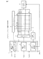
平面ディスプレイとしてプラズマディスプレイ装置が実用化されており、高輝度の薄型ディスプレイとして期待されている。図1は、従来の3電極型のAC駆動方式のプラズマディスプレイ装置の全体構成を示す図である。図示のように、プラズマディスプレイ装置は、隣接して配置した複数のX電極(X1,X2,X3,…,Xn)及びY電極(Y1,Y2,Y3,…,Yn)と、それに交差する方向に配置した複数のアドレス電極(A1,A2,A3,…,Am)と、交差部分に配置した蛍光体とを有する2枚の基板間に放電ガスを封入したプラズマディスプレイパネル(PDP)1と、アドレス電極にアドレスパルスなどを印加するアドレスドライバ2と、X電極に維持放電(サステイン)パルスなどを印加するX共通ドライバ3と、Y電極に順次走査パルスなどを印加する走査ドライバ4と、Y電極に印加する維持放電(サステイン)パルスなどを走査ドライバ4に供給するY共通ドライバ5と、各部の制御を行う制御回路6とを備え、制御回路6は、更にフレームメモリを含む表示データ制御部7と、走査ドライバ制御部9と共通ドライバ制御部10で構成される駆動制御回路8とを有する。X共通ドライバ3とY共通ドライバ5には、サステインパルスを出力するサステイン回路が設けられており、サステイン回路はサステイン出力素子を有する。プラズマディスプレイ装置については広く知られているので、ここでは装置全体に関するこれ以上の詳しい説明は省略し、本発明に関係するX共通ドライバ3とY共通ドライバ5についてのみ更に説明する。プラズマディスプレイ装置のX共通ドライバ、走査ドライバ及びY共通ドライバについては、例えば、特開2001−282181号公報及び特開2002−351388号公報などに開示されている。また、特開平8−335863号公報は、このようなドライバで使用されるパワートランジスタ駆動回路及びそれを1チップ化したICを開示している。
A plasma display device has been put to practical use as a flat display, and is expected as a thin display with high luminance. FIG. 1 is a diagram showing an overall configuration of a conventional three-electrode type AC driven plasma display device. As shown in the drawing, the plasma display device has a plurality of X electrodes (X1, X2, X3,..., Xn) and Y electrodes (Y1, Y2, Y3,. A plasma display panel (PDP) 1 in which a discharge gas is sealed between two substrates having a plurality of address electrodes (A1, A2, A3,..., Am) arranged in An
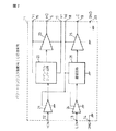
図2は、特開平8−335863号公報に開示されたパワートランジスタ駆動回路の概略構成をブロック図で表した図であり、破線で示すように全体がIC11に設けられている。プラズマディスプレイ装置では、図2のパワートランジスタ駆動ICを、サステイン出力素子をドライブするためのプリドライブ回路として使用する。図2に示すパワートランジスタ駆動IC11では、ハイレベル入力電圧HINを入力回路21で増幅し、ハイレベルシフト回路22によってハイレベル基準電圧Vrを基準とした電圧に変換し、更に出力増幅回路23を介してハイレベル出力電圧HOとして出力している。また、ローレベル入力電圧LINを入力増幅回路24で増幅し、遅延回路25を介して出力増幅回路26へ入力して増幅した後ローレベル出力電圧LOとして出力している。参照番号12と13はハイレベル入力電圧HINとローレベル入力電圧LINの入力端子を、参照番号16と19はハイレベル出力電圧HOとローレベル出力電圧LOの出力端子を、参照番号15はハイレベル電源電圧Vcの供給端子を、参照番号17はハイレベル基準電圧Vrの供給端子を、参照番号18はローレベル電源電圧Vdの供給端子を、参照番号20はグランド端子を示す。
FIG. 2 is a block diagram showing a schematic configuration of a power transistor driving circuit disclosed in Japanese Patent Application Laid-Open No. 8-335863. The whole is provided in the IC 11 as shown by a broken line. In the plasma display device, the power transistor driving IC of FIG. 2 is used as a pre-drive circuit for driving a sustain output element. In the power
図2のパワートランジスタ駆動ICにおいて、遅延回路25は、ハイレベル入力電圧HINとハイレベル出力電圧HOの立ち上がり時刻の差分tdLH(HO)と、ローレベル入力電圧LINとローレベル出力電圧LOの立ち上り時刻の差分tdLH(LO)が等しくなるように調整する働きをしている。更に、遅延回路25は、ハイレベル入力電圧HINとハイレベル出力電圧HOの立ち下がり時刻の差分tdHL(HO)と、ローレベル入力電圧LINとローレベル出力電圧LOの立ち下り時刻の差分tdHL(LO)が等しくなるように調整する働きもしている。しかしながら、遅延回路25によってtdLH(HO)とtdLH(LO)を完全に一致させることはできず、ある程度の差が生じるのが避けられない。同様に、tdHL(HO)とtdHL(LO)を完全に一致させることはできず、ある程度の差が生じるのが避けられない。
In the power transistor drive IC of FIG. 2, the
図2のパワートランジスタ駆動ICをプラズマディスプレイ装置のプリドライブ回路として使用する場合、その出力端子16,19には、パワーMOSFETやIGBT(Insulated Gate Bipolar Transistor)などのサステイン出力素子が接続される。プラズマディスプレイ装置(PDP装置)では、サステイン出力素子をオン・オフすることによってサステインパルスを生成し、プラズマディスプレイパネル(PDP)のX電極とY電極に供給している。
When the power transistor driving IC of FIG. 2 is used as a pre-drive circuit of a plasma display device, a sustain output element such as a power MOSFET or an IGBT (Insulated Gate Bipolar Transistor) is connected to its
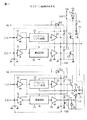
図3は、PDP装置におけるサステイン回路の一例を示しており、図2のパワートランジスタ駆動ICをサステイン出力素子のプリドライブ回路11A,11Bに使用する。図3において、CUとCDはサステイン出力素子を示し、この出力素子をオン・オフさせることによって、容量性負荷に相当するPDPへサステインパルスを供給している。図3において、入力信号CUIはプリドライブ回路11Aのハイレベル入力電圧として入力され、ハイレベル出力電圧として出力素子CUへ供給される。また、入力信号CDIはプリドライブ回路11Aのローレベル入力電圧として入力され、ローレベル出力電圧として出力素子CDへ供給される。
FIG. 3 shows an example of a sustain circuit in a PDP device. The power transistor driving IC of FIG. 2 is used for
出力素子CUがオンすると電源電圧Vsが、ダイオードD1と出力素子CUを介してPDPへ供給される(この時、出力素子CDはオフ)。また、出力素子CDがオンすると、この出力素子CDを介してPDPへグランド(GND)電圧が供給される(この時、出力素子CUはオフ)。なお、出力素子CUを駆動するプリドライブ回路11Aの電源電圧(容量C1に蓄えられるハイレベル電源電圧)は、電源VeからダイオードD2を介して、容量C1に充電される。また、出力素子CDを駆動するプリドライブ回路11Aの電源電圧(容量C2に蓄えられるローレベル電源電圧)は、電源Veから直接容量C2に充電される。図3に示した回路では、出力素子CU,CDを交互にオン・オフすることによって、PDPへサステインパルスを供給する。
When the output element CU is turned on, the power supply voltage Vs is supplied to the PDP via the diode D1 and the output element CU (at this time, the output element CD is turned off). When the output element CD is turned on, a ground (GND) voltage is supplied to the PDP via the output element CD (at this time, the output element CU is turned off). Note that the power supply voltage (high-level power supply voltage stored in the capacitor C1) of the
図3のLUとLDは電力回収出力素子であり、このLU、LDをオン・オフすることによって、CU、CDの電力を低減する働きをしている。図3において、入力信号LUIはプリドライブ回路のハイレベル入力電圧として入力され、ハイレベル出力電圧として出力素子LUに供給される。また、入力信号LDIはプリドライブ回路のローレベル入力電圧として入力され、ローレベル出力電圧として出力素子LDに供給される。 LU and LD in FIG. 3 are power recovery output elements, and function to reduce the power of the CU and CD by turning on and off the LU and LD. In FIG. 3, an input signal LUI is input as a high-level input voltage of the pre-drive circuit, and is supplied to the output element LU as a high-level output voltage. The input signal LDI is input as a low-level input voltage of the pre-drive circuit, and is supplied to the output element LD as a low-level output voltage.
出力素子LUがオンすると、電源電圧VsとGNDの間に直列に接続された容量C5とC6の中点電圧Vpが、出力素子LU、ダイオードD4、コイルL1を介してPDPに供給される(この時、出力素子LDはオフ)。また、出力素子LDがオンすると、コイルL2、ダイオードD5、出力素子LDを介してPDPに上記の中点電圧Vpが供給される(この時、出力素子LUはオフ)。なお、出力素子LUを駆動するプリドライブ回路の電源電圧(容量C3に蓄えられているハイレベル電源電圧)は、電源VeからダイオードD3を介して、容量C3に充電される。また、出力素子LDを駆動するプリドライブ回路の電源電圧(容量C4に蓄えられているローレベル電源電圧)は、電源Veから直接容量C4に充電される。図3に示した回路では、上記出力素子LUをサステイン出力素子CUがオンする直前にオンさせ、上記出力素子LDをサステイン出力素子CDがオンする直前にオンさせることによって、CU、CDで生じる電力損失を低減する働きをしている。 When the output element LU is turned on, the midpoint voltage Vp of the capacitors C5 and C6 connected in series between the power supply voltage Vs and GND is supplied to the PDP via the output element LU, the diode D4, and the coil L1. At this time, the output element LD is off). When the output element LD is turned on, the midpoint voltage Vp is supplied to the PDP via the coil L2, the diode D5, and the output element LD (at this time, the output element LU is turned off). The power supply voltage of the pre-drive circuit that drives the output element LU (high-level power supply voltage stored in the capacitor C3) is charged from the power supply Ve to the capacitor C3 via the diode D3. Further, the power supply voltage (low-level power supply voltage stored in the capacitor C4) of the predrive circuit that drives the output element LD is directly charged to the capacitor C4 from the power supply Ve. In the circuit shown in FIG. 3, the output element LU is turned on just before the sustain output element CU is turned on, and the output element LD is turned on just before the sustain output element CD is turned on, so that the electric power generated in the CU and CD is obtained. It works to reduce loss.
なお、図3に示した回路において、スイッチSW1は、プラズマディスプレイ装置のリセット期間にオンし、リセット電圧Vwを出力素子CUを介してPDPに供給する働きをしている。 In the circuit shown in FIG. 3, the switch SW1 is turned on during the reset period of the plasma display device, and functions to supply the reset voltage Vw to the PDP via the output element CU.
図2のパワートランジスタ駆動用ICを使用したプリドライブ回路では、遅延回路25によって、ハイレベル入力電圧HINとハイレベル出力電圧HOの立ち上がり時刻の差分tdLH(HO)、及び上記ローレベル入力電圧LINとローレベル出力電圧LOの立ち上がり時刻の差分tdLH(LO)との違いを調整している。しかしながら、プリドライブ回路におけるハイレベルシフト回路と、その回路での遅延時間に相当する時間遅延させる遅延回路とは、異なった回路であり、素子のばらつきや温度特性を含めた遅延特性を完全に一致させることはできない。この結果、上記tdLH(HO)とtdLH(LO)に差が生じるのが避けられない。
In the pre-drive circuit using the power transistor driving IC of FIG. 2, the difference tdLH (HO) between the rising time of the high-level input voltage HIN and the rising time of the high-level output voltage HO and the low-level input voltage LIN are determined by the
tdLH(HO)とtdLH(LO)に差があるプリドライブ回路を、図3に示したプラズマディスプレイ装置のサステイン回路に適用した場合、出力素子CUとCDのオン・オフのタイミングが、設計値とずれる可能性がある。このようなタイミングのずれが生じた場合、出力素子が同時にオンし、CUからCDに貫通電流が流れ、過電流による素子破壊に至る可能性がある。 When a pre-drive circuit having a difference between tdLH (HO) and tdLH (LO) is applied to the sustain circuit of the plasma display device shown in FIG. 3, the ON / OFF timing of the output elements CU and CD is different from the design value. May shift. When such a timing shift occurs, the output element is turned on at the same time, a through current flows from the CU to the CD, and the element may be destroyed due to an overcurrent.
また、同様に、電力回収出力素子LU、LDのオンするタイミングが設計値とずれる可能性もある。このタイミングのずれにより、立ち上がり時の電力回収電流(L1に流れる電流)と立ち下り時の電力回収電流(L2に流れる電流)がアンバランスになり、容量C5とC6の中点電圧Vpの値が中間電圧からずれ、電力回収動作が正常に行われず、消費電力が増加する可能性がある。 Similarly, the timing at which the power recovery output elements LU and LD are turned on may deviate from the design value. Due to this timing shift, the power recovery current at the rise (current flowing through L1) and the power recovery current at the fall (current flowing through L2) become unbalanced, and the value of the midpoint voltage Vp of the capacitances C5 and C6 decreases. The power recovery operation may not be performed normally due to deviation from the intermediate voltage, and power consumption may increase.
さらに、絶対値が等しい正負の電圧のサステインパルスを使用して駆動素子の耐圧を低下させることが行われているが、制御信号はグランドを基準電圧とする信号であり、上記のプリドライブ回路から負電圧の駆動信号を出力するには、プリドライブ回路のローレベル基準電圧を負サステイン電圧とすると共に、レベルシフト回路を設けて入力電圧信号を負サステイン電圧を基準電圧とする信号に変換する必要がある。レベルシフト回路と上記のプリドライブ回路は別の回路であるため、上記と同様の問題を生じる。 Further, the withstand voltage of the driving element is reduced by using a positive / negative voltage sustain pulse having the same absolute value.However, the control signal is a signal having the ground as a reference voltage. To output a negative drive signal, the low-level reference voltage of the pre-drive circuit must be used as the negative sustain voltage, and a level shift circuit must be provided to convert the input voltage signal to a signal that uses the negative sustain voltage as the reference voltage. There is. Since the level shift circuit and the pre-drive circuit are different circuits, the same problem as described above occurs.
近年、プラズマディスプレイ装置は、輝度向上を図るため、サステイン周期を短くして1フレーム内のサステインパルス数を増加することが望まれているが、サステイン周期が短くなると、上記の問題がより一層重要になる。 In recent years, it has been desired for plasma display devices to increase the number of sustain pulses in one frame by shortening the sustain period in order to improve the brightness. However, when the sustain period is shortened, the above problem becomes more important. become.
本発明は、ハイレベルとローレベルの出力電圧のタイミングのずれを低減したプリドライブ回路を実現し、それを使用した容量性負荷駆動回路及びプラズマディスプレイ装置における素子破壊や消費電力の増加を防止することを目的とする。 The present invention realizes a pre-drive circuit in which the timing difference between high-level and low-level output voltages is reduced, and prevents element destruction and increase in power consumption in a capacitive load drive circuit and a plasma display device using the same. The purpose is to:
上記目的を実現するため、本発明のプリドライブ回路は、入力増幅回路とハイレベルシフト回路と出力増幅回路とを有する同一構成の駆動系を複数備えることを特徴とする。 In order to achieve the above object, a predrive circuit according to the present invention includes a plurality of drive systems having the same configuration including an input amplifier circuit, a high-level shift circuit, and an output amplifier circuit.
図2の遅延回路25はハイレベルシフト回路22に比べて回路構成が簡単であり、回路規模を小さくできる。ローレベル電圧の駆動系は、増幅した入力電圧信号をハイレベルにシフトする必要はないので、従来のプリドライブ回路(パワートランジスタ駆動用IC)では、回路規模を小さくするために、遅延回路を使用していた。しかし、本発明者は、この構成では上記のような問題を生じることを発見した。
The circuit configuration of the
本発明のプリドライブ回路を使用すれば、同一構成の駆動系が複数設けられており、遅延回路の替わりにハイレベルシフト回路を使用してハイレベル電圧の駆動系とローレベル電圧の駆動系を同一の構成にできるので、タイミングのずれを生じない。従って、このプリドライブ回路を用いたICを使用すれば、出力素子CUとCDを駆動するゲートパルスの立ち上がりのタイミング及びゲートパルスの立ち下がりのタイミングを所望の状態に正確に設定することができる。従って、CUとCDが同時にオンすることにより生じる過電流による破壊を防止できる。 If the pre-drive circuit of the present invention is used, a plurality of drive systems having the same configuration are provided, and a high-level voltage drive system and a low-level voltage drive system are used by using a high-level shift circuit instead of the delay circuit. Since the same configuration can be used, no timing shift occurs. Therefore, if an IC using this pre-drive circuit is used, the rising timing of the gate pulse for driving the output elements CU and CD and the falling timing of the gate pulse can be accurately set to desired states. Therefore, it is possible to prevent the destruction due to the overcurrent caused when the CU and the CD are simultaneously turned on.
また、本発明のプリドライブ回路を使用すれば、出力素子LUとLDを駆動するゲートパルスの立ち上がりのタイミング及びゲートパルスの立ち下がりのタイミングを所望の状態に正確に設定することができる。従って、サステインパルスの立ち上がり時の電力回収(L1に流れる電流)と、サステインパルスの立ち下がり時の電力回収(L2に流れる電流)のアンバランスによる容量C5とC6の中間電圧Vpの変化を低減することができる。これによって、電力回収動作の異常による消費電力増加を防止することができる。 Further, if the pre-drive circuit of the present invention is used, the timing of the rise of the gate pulse and the timing of the fall of the gate pulse for driving the output elements LU and LD can be accurately set to a desired state. Therefore, a change in the intermediate voltage Vp between the capacitors C5 and C6 due to imbalance between the power recovery at the rising of the sustain pulse (current flowing through L1) and the power recovery at the falling of the sustain pulse (current flowing through L2) is reduced. be able to. This can prevent an increase in power consumption due to an abnormality in the power recovery operation.
レベルシフト回路は、そこに供給する基準電源電圧に応じて入力電圧をシフトさせる。従って、ローレベル電圧の駆動系を構成するレベルシフト回路には、それに応じた基準電源電圧を供給する。図2及び図3の例では、ローレベル電圧の駆動系の基準電源電圧はグランド(GND)であるが、後述するハイレベル出力電圧とローレベル出力電圧を絶対値が等しく正負逆の極性にする構成の場合、本発明のプリドライブ回路を使用して、一方の駆動系に正の基準電源電圧を、他方の駆動系に負の基準電源電圧を供給することも可能である。 The level shift circuit shifts an input voltage according to a reference power supply voltage supplied thereto. Accordingly, the reference power supply voltage is supplied to the level shift circuit constituting the low-level voltage driving system. In the examples of FIGS. 2 and 3, the reference power supply voltage of the drive system of the low-level voltage is ground (GND), but the high-level output voltage and the low-level output voltage, which will be described later, have the same absolute value and opposite polarity. In the case of the configuration, it is also possible to use the pre-drive circuit of the present invention to supply a positive reference power supply voltage to one drive system and a negative reference power supply voltage to the other drive system.
複数の駆動系は、同一の半導体チップ上に形成すること、すなわちIC化することが望ましい。これにより2つの駆動系の回路特性の同一性が一層高くなる。 It is desirable that a plurality of drive systems be formed on the same semiconductor chip, that is, integrated. As a result, the circuit characteristics of the two drive systems become more identical.
複数の駆動系の入力増幅回路の駆動電源を供給する入力増幅回路用電源電圧端子と、複数の駆動系の出力増幅回路の駆動電源を供給する出力増幅回路用電源電圧端子は別々に設けることが望ましい。 The power supply voltage terminal for the input amplifier circuit that supplies the drive power for the input amplifier circuits of the plurality of drive systems and the power supply voltage terminal for the output amplifier circuit that supplies the drive power supply for the output amplifier circuits of the plurality of drive systems can be provided separately. desirable.
複数の駆動系のそれぞれの入力電圧端子と入力増幅回路の間に、シュミットトリガ回路などの波形処理回路を設けてもよい。その場合、波形処理回路に別の電源電圧を供給する必要があり、波形処理回路用電源端子を設けるか、入力増幅回路用電源電圧端子に供給される電圧を変換して波形処理回路用電源電圧を生成する定電圧回路を設ける。 A waveform processing circuit such as a Schmitt trigger circuit may be provided between each input voltage terminal of the plurality of drive systems and the input amplifier circuit. In this case, it is necessary to supply another power supply voltage to the waveform processing circuit. A power supply terminal for the waveform processing circuit is provided, or the voltage supplied to the power supply voltage terminal for the input amplifier circuit is converted to supply the power supply voltage for the waveform processing circuit. Is provided.
駆動系の個数は、2つ又は4つであることが望ましい。 It is desirable that the number of drive systems is two or four.
2つの駆動系を有するプリドライブ回路(用IC)を使用してプラズマディスプレイ装置のサステイン回路のような容量性負荷駆動回路を構成する場合には、2つの駆動系を有するプリドライブ回路と、一方の駆動系の出力増幅回路の出力に接続された第1のスイッチ素子(CU)と、他方の駆動系の出力増幅回路の出力に接続された第2のスイッチ素子(CD)とを設け、第1のスイッチ素子を介して容量性負荷にハイレベル電圧を供給し、第2のスイッチ素子を介して容量性負荷にローレベル電圧を供給する。この容量性負荷駆動回路に電力回収回路を設ける場合には、更に2つの駆動系を有する第2のプリドライブ回路を設け、第2のプリドライブ回路の一方の駆動系の出力増幅回路の出力に接続された第3のスイッチ素子(LU)と、他方の駆動系の出力増幅回路の出力に接続された第4のスイッチ素子(LD)とを設け、第3のスイッチ素子と第1のコイルを介して容量性負荷にハイレベル電圧を供給し、第4のスイッチ素子と第2のコイルを介して容量性負荷にローレベル電圧を供給する。 When a capacitive load drive circuit such as a sustain circuit of a plasma display device is configured using a predrive circuit (IC) having two drive systems, a predrive circuit having two drive systems, A first switch element (CU) connected to the output of the output amplifier circuit of the other drive system, and a second switch element (CD) connected to the output of the output amplifier circuit of the other drive system. A high-level voltage is supplied to the capacitive load via one switch element, and a low-level voltage is supplied to the capacitive load via the second switch element. When a power recovery circuit is provided in this capacitive load drive circuit, a second predrive circuit having two drive systems is further provided, and an output amplifier circuit of one drive system of the second predrive circuit is provided. A third switch element (LU) connected thereto and a fourth switch element (LD) connected to the output of the output amplifier circuit of the other drive system, and the third switch element and the first coil are connected to each other. A high-level voltage is supplied to the capacitive load via the first switch element, and a low-level voltage is supplied to the capacitive load via the fourth switch element and the second coil.
4つの駆動系を有するプリドライブ回路を使用して電力回収回路を有する容量性負荷駆動回路を構成する場合には、4つの出力増幅回路の出力に第1から第4のスイッチ素子をそれぞれ接続する。 When a capacitive load drive circuit having a power recovery circuit is configured using a pre-drive circuit having four drive systems, first to fourth switch elements are respectively connected to the outputs of the four output amplifier circuits. .
なお、タイミングを一層正確に調整するために、プリドライブ回路の前段又は後段に、信号の入出力時間を調整する遅延時間調整回路を設けることが望ましい。遅延時間調整回路は、例えば、複数の抵抗値から使用する抵抗値を選択する可変抵抗と容量の組合せで実現される。選択できる抵抗値の個数が同じ場合、選択できる抵抗値の範囲が小さいほど抵抗値を細かく調整できる。本発明によれば、従来例に比べてタイミングのずれの範囲を小さくできるので、より細かな調整が可能である。 In order to more accurately adjust the timing, it is desirable to provide a delay time adjusting circuit for adjusting the input / output time of the signal at a stage before or after the pre-drive circuit. The delay time adjustment circuit is realized by, for example, a combination of a variable resistor and a capacitor for selecting a resistance value to be used from a plurality of resistance values. When the number of selectable resistance values is the same, the smaller the range of selectable resistance values, the finer the resistance value can be adjusted. According to the present invention, the range of the timing shift can be reduced as compared with the conventional example, so that finer adjustment is possible.
第3のスイッチ素子の容量性負荷に接続されない端子に、ハイレベル電圧とローレベル電圧の中間電圧以外の電圧を供給してもよい。 A voltage other than the intermediate voltage between the high-level voltage and the low-level voltage may be supplied to a terminal of the third switch element that is not connected to the capacitive load.
ハイレベル電圧とローレベル電圧は任意に設定可能であり、例えば、ハイレベル電圧を電源電圧、ローレベル電圧をグランド電圧とするか、ハイレベル電圧は正の電圧とし、ローレベル電圧はハイレベル電圧と同じ絶対値で負の電圧とする。 The high-level voltage and the low-level voltage can be set arbitrarily. For example, the high-level voltage is a power supply voltage, the low-level voltage is a ground voltage, or the high-level voltage is a positive voltage, and the low-level voltage is a high-level voltage. A negative voltage with the same absolute value as.
ローレベル出力電圧が負電圧の場合、プリドライブ回路の複数の入力電圧端子の前段に、グランド電圧を基準とした入力信号を、ローレベル電圧を基準とした信号にレベル変換する入力レベルシフト回路を設ける。 If the low-level output voltage is a negative voltage, an input level shift circuit that converts the level of an input signal based on the ground voltage into a signal based on the low-level voltage is provided before the input voltage terminals of the pre-drive circuit. Provide.
さらに、上記の入力レベルシフト回路や波形処理回路を設ける場合には、これらの回路をプリドライブ回路内に設けることが望ましい。これにより、これらの回路をプリドライブ回路と別に設けた場合に生じる出力電圧のタイミングのずれを低減することが可能になる。 Further, when the input level shift circuit and the waveform processing circuit described above are provided, it is desirable to provide these circuits in the pre-drive circuit. As a result, it is possible to reduce the shift in the output voltage timing that occurs when these circuits are provided separately from the pre-drive circuit.
なお、入力レベルシフト回路や波形処理回路をプリドライブ回路内に設ける場合にも、上記の構成を適用することが望ましい。例えば、各回路の電源端子を別にすることが望ましく、入力レベルシフト回路や波形処理回路を有するプリドライブ回路は、1パッケージ内に形成するか、特に同一の半導体チップ上に形成すること、すなわちIC化することが望ましい。 Note that it is desirable to apply the above configuration also when providing an input level shift circuit and a waveform processing circuit in a pre-drive circuit. For example, it is desirable to provide a separate power supply terminal for each circuit, and a pre-drive circuit having an input level shift circuit and a waveform processing circuit is formed in one package, or in particular, formed on the same semiconductor chip, that is, an IC. Is desirable.
また、波形処理回路に積分回路を設けてノイズを除去できるようにすることが望ましい。 It is also desirable to provide an integration circuit in the waveform processing circuit so that noise can be removed.
さらに、対となる2個の駆動素子の駆動信号を出力する対の2つの駆動系の一方の出力がアクティブ状態の時には、他方の出力を強制的にノンアクティブ状態に維持する同時オン防止回路を設けることが望ましい。 Further, a simultaneous ON prevention circuit for forcibly maintaining the other output in a non-active state when one output of two drive systems of the pair outputting drive signals of two drive elements forming a pair is in an active state. It is desirable to provide.
本発明によれば、プリドライブ回路のハイレベル側とローレベル側の間で生じる入出力遅延時間の差を低減することができる。また、このプリドライブ回路を用いた容量性負荷駆動回路をプラズマディスプレイ装置に適用することにより、入出力遅延時間の差によって生じる素子破壊や消費電力の増加を防止できる。 According to the present invention, it is possible to reduce a difference in input / output delay time generated between the high level side and the low level side of the pre-drive circuit. Further, by applying a capacitive load driving circuit using this pre-drive circuit to a plasma display device, it is possible to prevent element destruction and increase in power consumption caused by a difference in input / output delay time.
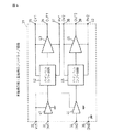
図4は、本発明の第1実施例のプリドライブ回路の構成を示す図である。図4に示すように、第1入力増幅回路41と第2入力増幅回路44、第1ハイレベルシフト回路42と第2ハイレベルシフト回路45、第1出力増幅回路43と第2出力増幅回路46は、それぞれ同一の回路で構成されている。この結果、第1入力電圧IN1と第1出力電圧OUT1の立ち上がり時刻の差tdLH1と、第2入力電圧IN2と第2出力電圧OUT2の立ち上がり時刻の差tdLH2の差分(tdLH1−tdLH2)を、図2に示した従来のパワートランジスタ駆動用IC(プリドライブ回路)より小さくすることができる。また、同様に、IN1とOUT1の立ち下がり時刻の差tdHL1と、IN2とOUT2の立ち下がり時刻の差tdHL2の差分(tdHL1−tdHL2)を、図2に示した従来のプリドライブ回路より小さくすることができる。
FIG. 4 is a diagram showing a configuration of the pre-drive circuit according to the first embodiment of the present invention. As shown in FIG. 4, the
このプリドライブ回路を、破線で示したパッケージ内に、特にIC(集積回路)11内に形成することにより、回路内の素子のばらつきを減らすことができ、上記差分(tdLH1−tdLH2)及び(tdHL1−tdHL2)をより小さくできる。 By forming this pre-drive circuit in a package indicated by a broken line, particularly in an IC (integrated circuit) 11, variations in elements in the circuit can be reduced, and the differences (tdLH1-tdLH2) and (tdHL1) −tdHL2) can be made smaller.
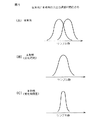
図5は、本発明のプリドライブ回路による効果、すなわちタイミングのずれの低減を説明する図である。図5の(A)と(B)は、製造した回路をサンプリングして求めた入出力遅延時間(入力電圧の立ち上がり時刻と出力電圧の立ち上がり時刻の差)の分布の例を示している。図5の(A)に示すように、従来はハイレベル電圧の駆動系はハイレベルシフト回路を有し、ローレベル電圧の駆動系は遅延回路を有し、2つの回路は異なる構成であるので、入出力遅延時間は異なる値を中心にばらつくことになる。従って、2つの駆動系の入出力遅延時間の差は中心値の差を中心にしてばらつき、絶対値が大きくなる。これに対して、本発明によれば、ハイレベル電圧とローレベル電圧の2つの駆動系は同一の構成を有するので、図5の(B)に示すように同じ値を中心にしてばらつくことになるので、2つの駆動系の入出力遅延時間の差はゼロを中心にばらつくことになり、絶対値は従来例に比べて小さくなる。 FIG. 5 is a diagram illustrating the effect of the pre-drive circuit of the present invention, that is, the reduction of the timing shift. FIGS. 5A and 5B show examples of the distribution of input / output delay times (difference between the rise time of the input voltage and the rise time of the output voltage) obtained by sampling the manufactured circuit. As shown in FIG. 5A, conventionally, a high-level voltage driving system has a high-level shift circuit, a low-level voltage driving system has a delay circuit, and the two circuits have different configurations. However, the input / output delay time varies around different values. Therefore, the difference between the input and output delay times of the two drive systems varies around the difference between the center values, and the absolute value increases. On the other hand, according to the present invention, since the two driving systems of the high-level voltage and the low-level voltage have the same configuration, they vary around the same value as shown in FIG. Therefore, the difference between the input and output delay times of the two drive systems varies around zero, and the absolute value is smaller than in the conventional example.
更に、プリドライブ回路の2つの駆動系を同一パッケージ又はIC内に形成した場合、同一構成の2つの駆動系の入出力遅延時間は類似の傾向を示すと考えられるので、2つの駆動系の入出力遅延時間の差は図5の(C)に示すように一層小さくなる。このように、本発明によれば、2つの駆動系の入出力遅延時間の差を非常に小さくできる。 Further, when two driving systems of the pre-drive circuit are formed in the same package or IC, the input / output delay times of the two driving systems having the same configuration are considered to have a similar tendency. The difference between the output delay times becomes smaller as shown in FIG. Thus, according to the present invention, the difference between the input and output delay times of the two drive systems can be made very small.
また、図2に示した従来のプリドライブ回路では、第1及び第2の入力増幅回路21,24の電源電圧として、ローレベル電源電圧を利用していた。この結果、例えば入力電圧HINに対して出力電圧HOを出力するハイレベル電圧の駆動系のみを利用する場合でも、ローレベル電源電圧を入力する必要があった。これに対して、図4に示した第1実施例のプリドライブ回路では、独立した入力増幅回路用電源電圧入力端子VI132を設けて入力増幅回路41,42の電源電圧を供給している。この結果、例えば、ハイレベル電圧の駆動系のみを利用する場合には、第2の出力増幅回路46の電源電圧を供給する必要がなく、入力部と出力部を独立に設計できる。
In the conventional pre-drive circuit shown in FIG. 2, a low-level power supply voltage is used as the power supply voltage for the first and second
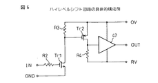
図6は、第1実施例のプリドライブ回路の入力増幅回路とハイレベルシフト回路の具体的構成を示す図である。入力電圧INは抵抗R2を介してトランジスタTr1のゲートに印加される。トランジスタTr1のドレインは抵抗R3を介してハイレベル電源電圧OVに接続され、入力電圧に応じてTr1と抵抗R3の接続点に電圧信号を生じる。この電圧信号は、ハイレベル電源電圧OVと抵抗R4を介してハイレベル基準電源RVに接続されたトランジスタTr2のゲートに印加される。これによりTr2と抵抗R4の接続点には、ハイレベル基準電源RVを基準に変化する電圧が発生し、この電圧が出力増幅回路47に供給される。なお、ハイレベルシフト回路は広く使用されており、そのいずれも使用でき、例えば前述の特開平8−335863号公報に開示されたハイレベルシフト回路も使用可能である。
FIG. 6 is a diagram showing a specific configuration of the input amplifier circuit and the high level shift circuit of the pre-drive circuit of the first embodiment. The input voltage IN is applied to the gate of the transistor Tr1 via the resistor R2. The drain of the transistor Tr1 is connected to the high-level power supply voltage OV via the resistor R3, and generates a voltage signal at the connection point between the transistor Tr1 and the resistor R3 according to the input voltage. This voltage signal is applied to the gate of the transistor Tr2 connected to the high-level reference power supply RV via the high-level power supply voltage OV and the resistor R4. As a result, a voltage that changes with reference to the high-level reference power supply RV is generated at the connection point between the transistor Tr2 and the resistor R4, and this voltage is supplied to the
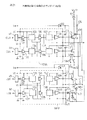
図7は、本発明の第2実施例のプラズマディスプレイ装置のサステイン回路の構成を示す。図示のように、第2実施例のサステイン回路は、図3の従来のサステイン回路と類似の構成を有するが、出力素子CU、CD、LU、LDを駆動するプリドライブ回路を第1実施例のプリドライブ回路を使用して実現した点が異なる。 FIG. 7 shows a configuration of a sustain circuit of a plasma display device according to a second embodiment of the present invention. As shown, the sustain circuit of the second embodiment has a configuration similar to that of the conventional sustain circuit of FIG. 3, except that a pre-drive circuit for driving the output elements CU, CD, LU, and LD is provided in the first embodiment. The difference is that it is realized using a pre-drive circuit.
図7に示すように、サステイン回路のプリドライブ回路として、図4のプリドライブ回路を使用することにより、出力素子CU、CDに供給するゲートパルスの立ち上がり時刻と立下り時刻をより正確に設定できる。この結果、出力素子CU、CDが同時にオンになって貫通電流により出力素子CU、CDが破壊される可能性を低減できる。また、出力素子LU、LDに供給するゲートパルスの立ち上がり時刻と立ち下り時刻をより正確に設定できる。この結果、出力素子LU、LDのオンするタイミングを正確に設定でき、コイルL1を介して流れる電力回収電流と、コイルL2を介して流れる電力回収電流の値を適切に設定することができる。これにより、出力素子LU、LDのオンするタイミングのずれによって生じる消費電力の増加を抑えることができる。 As shown in FIG. 7, the rise time and fall time of the gate pulse supplied to the output elements CU and CD can be set more accurately by using the predrive circuit of FIG. 4 as the predrive circuit of the sustain circuit. . As a result, it is possible to reduce the possibility that the output elements CU and CD are simultaneously turned on and the output elements CU and CD are destroyed by the through current. Further, the rise time and fall time of the gate pulse supplied to the output elements LU and LD can be set more accurately. As a result, the timing at which the output elements LU and LD are turned on can be accurately set, and the value of the power recovery current flowing through the coil L1 and the value of the power recovery current flowing through the coil L2 can be appropriately set. Thus, it is possible to suppress an increase in power consumption caused by a shift in the timing at which the output elements LU and LD are turned on.
図8は、本発明の第3実施例のプラズマディスプレイ装置のサステイン回路の構成を示す。図示のように、第3実施例のサステイン回路は、第2実施例のサステイン回路において、各入力電圧信号CUI、CDI、LUI、LDIの入力部に入出力遅延時間調整回路47〜50を設けた点が異なる。入出力遅延時間調整回路47〜50は、プリドライブ回路の入出力遅延時間のばらつきを吸収し、CUIとVG1、CDIとVG2、LUIとVG3、LDIとVG4との立ち上がり時刻又は立ち下がり時刻の差を小さくする働きをしている。
FIG. 8 shows a configuration of a sustain circuit of a plasma display device according to a third embodiment of the present invention. As shown in the drawing, the sustain circuit of the third embodiment is different from the sustain circuit of the second embodiment in that input / output delay
入出力遅延時間調整回路は、例えば、図9に示すような可変抵抗VRと容量Cによる遅延回路で実現できる。入出力遅延時間調整回路の構成は、特開2001−282181号公報に開示されているので、ここでは詳しい説明を省略する。 The input / output delay time adjustment circuit can be realized by, for example, a delay circuit including a variable resistor VR and a capacitor C as shown in FIG. Since the configuration of the input / output delay time adjustment circuit is disclosed in Japanese Patent Application Laid-Open No. 2001-282181, detailed description is omitted here.
また、第3実施例で使用するプリドライブ回路では、第1入力増幅回路41と第2入力増幅回路44の閾値電圧は、電源電圧の中間の電圧VI1/2に略等しく設定されている。これにより、入出力遅延時間調整回路47〜50を設けることにより生じるパルス幅の変化を低減できる。
In the pre-drive circuit used in the third embodiment, the threshold voltages of the
第3実施例の回路では、図4に示した第1実施例のプリドライブ回路を使用することにより、入出力遅延時間調整回路で調整する前の入出力遅延時間のばらつきを低減することができる。この結果、入出力遅延時間調整回路の調整範囲を小さくすることができる。例えば、入出力遅延時間調整回路として図9のような遅延回路を使用した場合、抵抗の可変範囲を小さくすることができる。従って、可変抵抗VRの抵抗の値をトリミングして抵抗値を変化させて遅延時間を変化させる場合、単位トリミング量によって設定できる遅延時間の最小調整量をより小さくできる。よって、より高精度な遅延時間の設定が可能となる。 In the circuit of the third embodiment, by using the pre-drive circuit of the first embodiment shown in FIG. 4, it is possible to reduce the variation of the input / output delay time before being adjusted by the input / output delay time adjustment circuit. . As a result, the adjustment range of the input / output delay time adjustment circuit can be reduced. For example, when a delay circuit as shown in FIG. 9 is used as the input / output delay time adjustment circuit, the variable range of the resistance can be reduced. Therefore, when the delay time is changed by trimming the resistance value of the variable resistor VR and changing the resistance value, the minimum adjustment amount of the delay time that can be set by the unit trimming amount can be further reduced. Therefore, it is possible to set the delay time with higher accuracy.
また、入出力遅延時間調整回路の調整範囲を小さくすることによって、部品ばらつきによって、規格外となる不良品の数を減らすことができ、生産性の向上が図れる。 In addition, by reducing the adjustment range of the input / output delay time adjustment circuit, the number of defective products out of the standard due to component variations can be reduced, and the productivity can be improved.
図10は、本発明の第4実施例のプラズマディスプレイ装置のサステイン回路の構成を示す。図示のように、第4実施例のサステイン回路は、第3実施例のサステイン回路において、リセット電圧源を出力素子CDの基準電圧側に接続する点が異なる。図10に示すように、出力素子CDの基準電圧側(PDPに接続されない側)を、スイッチSW2を介して電圧Vw’の電圧源に、スイッチSW3を介してGNDに接続する。容量C6のC5に接続されない側の端子は、容量C8を介して出力素子CUの電源側に接続する。当然スイッチSW1は除去する。PDPにリセット電圧Vwを印加する場合には、出力素子CUをオンして、スイッチSW3をオフした上で、スイッチSW2をオンする。これにより容量C8の端子の電圧がGNDからVw’に変化し、出力素子CUの電源側の電圧にVw’が重畳されてリセット電圧Vs+Vw’(=Vw)になる。このリセット電圧Vs+Vw’が出力素子CUを介してPDPに印加される。この時、出力素子CDの両端にはリセット電圧Vs+Vw’とVw’が印加されるので、出力素子CDに印加される電圧はVsであり、比較的耐圧の小さい出力素子CDを使用できるという利点がある。 FIG. 10 shows a configuration of a sustain circuit of a plasma display device according to a fourth embodiment of the present invention. As shown, the sustain circuit of the fourth embodiment differs from the sustain circuit of the third embodiment in that a reset voltage source is connected to the reference voltage side of the output element CD. As shown in FIG. 10, the reference voltage side (the side not connected to the PDP) of the output element CD is connected to the voltage source of the voltage Vw 'via the switch SW2 and to GND via the switch SW3. The terminal of the capacitor C6 on the side not connected to C5 is connected to the power supply side of the output element CU via the capacitor C8. Of course, the switch SW1 is removed. When applying the reset voltage Vw to the PDP, the output element CU is turned on, the switch SW3 is turned off, and then the switch SW2 is turned on. As a result, the voltage at the terminal of the capacitor C8 changes from GND to Vw ', and Vw' is superimposed on the voltage on the power supply side of the output element CU to become the reset voltage Vs + Vw '(= Vw). This reset voltage Vs + Vw 'is applied to the PDP via the output element CU. At this time, since the reset voltages Vs + Vw ′ and Vw ′ are applied to both ends of the output element CD, the voltage applied to the output element CD is Vs, and there is an advantage that the output element CD having a relatively small withstand voltage can be used. is there.
VsにVw’を重畳してリセット電圧Vs+Vw’を生成する構成については、特開2002−351388号公報に詳細が開示されている。 The configuration for generating the reset voltage Vs + Vw 'by superimposing Vw' on Vs is disclosed in detail in JP-A-2002-351388.
更に説明すれば、第4実施例のサステイン回路の特徴は、プリドライブ回路として図7の第1実施例の回路を使用した場合に比べて、電圧Vw’を出力素子CDの基準電圧側に印加できる点である。図3に示した従来のプリドライブ回路では、出力素子CDの基準電圧側はGNDであり、プリドライブ回路のローサイド基準電圧もGNDに接続されていた。また、従来のプリドライブ回路をICを用いて構成した場合、IC内部で入力部のGNDと接続されていたり、IC内のサブストレート(基板)に接続されていた。このため、図3に示した従来のプリドライブ回路では、ローサイド基準電圧をGNDより高くすることができなかった。よって、電圧Vw’を出力素子CDの基準電圧側に重畳することができなかった。 More specifically, the feature of the sustain circuit of the fourth embodiment is that the voltage Vw 'is applied to the reference voltage side of the output element CD as compared with the case where the circuit of the first embodiment in FIG. 7 is used as a pre-drive circuit. It is possible. In the conventional pre-drive circuit shown in FIG. 3, the reference voltage side of the output element CD is GND, and the low-side reference voltage of the pre-drive circuit is also connected to GND. Further, when a conventional pre-drive circuit is configured using an IC, it is connected to the GND of the input unit inside the IC or to a substrate (substrate) inside the IC. For this reason, in the conventional pre-drive circuit shown in FIG. 3, the low-side reference voltage cannot be made higher than GND. Therefore, the voltage Vw 'could not be superimposed on the reference voltage side of the output element CD.
これに対して、図4に示した第1実施例のプリドライブ回路における出力基準電圧端子RV2は、IC内でGNDには接続されていない。また、ICのサブストレートにも接続されていない。このため、出力基準電圧端子に電圧Vw’を重畳することが可能になる。 On the other hand, the output reference voltage terminal RV2 in the pre-drive circuit of the first embodiment shown in FIG. 4 is not connected to GND in the IC. Also, it is not connected to the IC substrate. Therefore, the voltage Vw 'can be superimposed on the output reference voltage terminal.
通常、リセット電圧Vwはサステイン回路の電源電圧Vsより高い。よって、図8に示したサステイン回路では、リセット電圧Vwを出力素子CUの電源側からPDPに供給していたため、出力素子CDにはリセット電圧に対応した電圧定格の高い素子を用いる必要があった。これに対して、図10の第4実施例のサステイン回路では、電圧Vw’を出力素子CDの基準電圧側から供給するため、出力素子CDにかかる電圧を小さくできる。よって、出力素子CDとして電圧定格が低く、チップサイズが小さい低コストの素子を使用できる。 Normally, the reset voltage Vw is higher than the power supply voltage Vs of the sustain circuit. Therefore, in the sustain circuit shown in FIG. 8, since the reset voltage Vw is supplied from the power supply side of the output element CU to the PDP, it is necessary to use an element having a high voltage rating corresponding to the reset voltage as the output element CD. . In contrast, in the sustain circuit of the fourth embodiment shown in FIG. 10, the voltage applied to the output element CD can be reduced because the voltage Vw 'is supplied from the reference voltage side of the output element CD. Therefore, a low-cost element having a low voltage rating and a small chip size can be used as the output element CD.
また、図10の回路では、図3において使用した容量C7、抵抗R1、ダイオードD6を削除している。図4に示した第1実施例のプリドライブ回路を用いることにより、電力回収出力素子LDを駆動するゲートパルスを、LDの基準電圧(電圧Vp)を基準としたパルスにレベルシフトできる。このため、容量C7、抵抗R1、ダイオードD6の削除が可能になる。図2に示した従来のプリドライブ回路を用いた場合、ローサイド基準電圧端子はIC内でGNDに接続されているため、容量C7、抵抗R1、ダイオードD6からなるレベルシフト回路が必要となる。図4に示した第1実施例のプリドライブ回路を用いることにより、このようなレベルシフト回路を削除できる効果がある。 In the circuit of FIG. 10, the capacitor C7, the resistor R1, and the diode D6 used in FIG. 3 are deleted. By using the pre-drive circuit of the first embodiment shown in FIG. 4, a gate pulse for driving the power recovery output element LD can be level-shifted to a pulse based on a reference voltage (voltage Vp) of the LD. Therefore, the capacitance C7, the resistor R1, and the diode D6 can be eliminated. When the conventional pre-drive circuit shown in FIG. 2 is used, since the low-side reference voltage terminal is connected to GND in the IC, a level shift circuit including a capacitor C7, a resistor R1, and a diode D6 is required. By using the pre-drive circuit of the first embodiment shown in FIG. 4, there is an effect that such a level shift circuit can be eliminated.
図11は、本発明の第5実施例のプラズマディスプレイ装置のサステイン回路の構成を示す。第5実施例のサステイン回路は、第1実施例のプリドライブ回路を使用したサステイン回路の別の例である。第5実施例のサステイン回路では、サステイン回路の電源電圧として、電圧Vs/2と−Vs/2の2電圧を利用する。図11の回路において、CUをオンすることによりVs/2をPDPに供給し、CDをオンすることにより−Vs/2をPDPに供給する。この際、CDの基準電圧は、−Vs/2となる。図11の回路では、プリドライブ回路の入力端子に供給する信号を、電圧−Vs/2を基準とした信号に変換するため、入力レベルシフト回路51−54を使用している。また、図11の回路では、図10で使用した容量C5とC6を削除し、電力回収用電圧Vp2として、GND電圧を利用している。サステイン動作時には、スイッチSW5がオンとなり、電圧VpはGND電圧となる。また、リセット期間には、スイッチSW5がオフとなり、スイッチSW1、SW4がオンとなる。この結果、CUを介してPDPにリセット電圧Vwが供給されるのと同時に、LDの基準電圧端子に電圧Vw2が供給される。スイッチSW4、SW5を使用して、電圧Vw2をLDの基準電圧端子に供給することにより、出力素子LDにかかる電圧を低減することができ、LDに電圧定格が低い(チップサイズが小さい低コストの)素子を利用することができる。このスイッチSW4、SW5を使用して、LDの電圧定格を低くする構成については、特願2002−141845号に開示されている。
FIG. 11 shows a configuration of a sustain circuit of a plasma display device according to a fifth embodiment of the present invention. The sustain circuit of the fifth embodiment is another example of the sustain circuit using the pre-drive circuit of the first embodiment. In the sustain circuit of the fifth embodiment, two voltages Vs / 2 and -Vs / 2 are used as the power supply voltage of the sustain circuit. In the circuit of FIG. 11, Vs / 2 is supplied to the PDP by turning on the CU, and -Vs / 2 is supplied to the PDP by turning on the CD. At this time, the reference voltage of the CD is -Vs / 2. In the circuit of FIG. 11, the input
図11に示した第5実施例の回路では、プリドライブ回路として図4に示した回路を用いている。従来のプリドライブ回路では、ローレベル基準電圧が、入力側の基準電圧と接続されているため、LDの基準電圧を入力側の基準電圧より高くすることができない。これに対して、図4に示したプリドライブ回路を適用することにより、LDの基準電圧を入力側の基準電圧−Vs/2より高くすることができる。 In the circuit of the fifth embodiment shown in FIG. 11, the circuit shown in FIG. 4 is used as a pre-drive circuit. In the conventional predrive circuit, since the low-level reference voltage is connected to the input-side reference voltage, the LD reference voltage cannot be made higher than the input-side reference voltage. On the other hand, by applying the pre-drive circuit shown in FIG. 4, the reference voltage of the LD can be made higher than the reference voltage −Vs / 2 on the input side.
なお、入力レベルシフト回路は、第1実施例のプリドライブ回路と一緒にIC内に形成してもよい。 Note that the input level shift circuit may be formed in an IC together with the pre-drive circuit of the first embodiment.
図11に示したように、サステイン電圧として、Vs/2と−Vs/2を使用したサステイン回路では、電力回収用の容量C5とC6を削除できる。また、スイッチSW4とSW5を使用することにより、LDに電圧定格の小さい素子を使用できる。 As shown in FIG. 11, in the sustain circuit using Vs / 2 and -Vs / 2 as the sustain voltage, the power recovery capacitors C5 and C6 can be omitted. Further, by using the switches SW4 and SW5, an element having a small voltage rating can be used for the LD.
図12は、入力レベルシフト回路の構成例を示す図である。図示のように、この回路は、トランジスタTr3を抵抗R5とR6を介して入力電源電圧5Vと−Vs/2の間に接続した回路である。入力レベルシフト回路については広く知られているので、ここでは詳しい説明を省略する。 FIG. 12 is a diagram illustrating a configuration example of the input level shift circuit. As shown, this circuit is a circuit in which a transistor Tr3 is connected between an input power supply voltage of 5 V and -Vs / 2 via resistors R5 and R6. Since the input level shift circuit is widely known, a detailed description is omitted here.
図13は、本発明の第6実施例のプラズマディスプレイ装置のサステイン回路の構成を示す。第6実施例のサステイン回路は、第5実施例のサステイン回路において、リセット電圧源を出力素子CDの基準電圧側に接続する点が異なる。リセット電圧源を出力素子CDの基準電圧側に接続する構成の利点は、第4実施例で説明した通りである。 FIG. 13 shows a configuration of a sustain circuit of a plasma display device according to a sixth embodiment of the present invention. The sustain circuit of the sixth embodiment is different from the sustain circuit of the fifth embodiment in that a reset voltage source is connected to the reference voltage side of the output element CD. The advantage of the configuration in which the reset voltage source is connected to the reference voltage side of the output element CD is as described in the fourth embodiment.
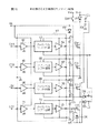
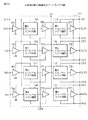
図14は、本発明の第7実施例のプリドライブ回路の構成を示す図である。第7実施例のプリドライブ回路は、4つの駆動系を有し、4入力及び4出力を有する点が特徴である。各駆動系は同一の回路構成で、第1実施例のプリドライブ回路の各駆動系と同じ構成を有する。従って、図5の(A)から(C)で説明した原理により、各回路における入出力遅延時間(立ち上がり時刻の差、立ち下がり時刻の差)の差分を小さくすることができる。 FIG. 14 is a diagram showing a configuration of a pre-drive circuit according to a seventh embodiment of the present invention. The pre-drive circuit of the seventh embodiment is characterized in that it has four drive systems and has four inputs and four outputs. Each drive system has the same circuit configuration and the same configuration as each drive system of the pre-drive circuit of the first embodiment. Therefore, according to the principle described in FIGS. 5A to 5C, it is possible to reduce the difference between the input and output delay times (the difference between the rising time and the falling time) in each circuit.
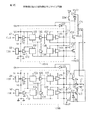
図15は、本発明の第8実施例のプラズマディスプレイ装置のサステイン回路の構成を示す。図示のように、第8実施例のサステイン回路は、図3の従来のサステイン回路において、出力素子CU、CD、LU、LDを駆動するプリドライブ回路に第7実施例のプリドライブ回路を使用して実現した点が異なる。第7実施例のプリドライブ回路を使用することにより、出力素子CU、CD、LU、LDを1個のプリドライブ回路で駆動することができる。従って、出力素子CUとCDのオン・オフのタイミングのずれによる破壊や、出力素子LUとLDのオンタイミングのずれによる電力回収動作の異常を防止することができる。特に、4駆動系をICに内蔵した場合には、LUとCU、LDとCDのオンするタイミングの差をより高精度に調整することができる。従って、電力回収動作をより高精度に行うことができる。また、図15には示していないが、図10のように入力端子の前段に入出力遅延時間調整回路47−50を設ける場合、調整範囲をより小さくして入出力遅延時間のより高精度な設定が可能となる。 FIG. 15 shows a configuration of a sustain circuit of a plasma display device according to an eighth embodiment of the present invention. As shown, the sustain circuit of the eighth embodiment uses the pre-drive circuit of the seventh embodiment as a pre-drive circuit for driving the output elements CU, CD, LU, and LD in the conventional sustain circuit of FIG. It is different in the point realized. By using the pre-drive circuit of the seventh embodiment, the output elements CU, CD, LU, and LD can be driven by one pre-drive circuit. Accordingly, it is possible to prevent the destruction due to the difference between the ON / OFF timings of the output elements CU and CD and the abnormality of the power recovery operation due to the difference between the ON timings of the output elements LU and LD. In particular, when the four drive systems are built in the IC, the difference between the ON timing of the LU and the CU, and the difference between the ON timings of the LD and the CD can be adjusted with higher accuracy. Therefore, the power recovery operation can be performed with higher accuracy. Although not shown in FIG. 15, when the input / output delay time adjustment circuit 47-50 is provided in the preceding stage of the input terminal as shown in FIG. 10, the adjustment range is made smaller to make the input / output delay time more accurate. Settings can be made.
図16は、本発明の第9実施例のプリドライブ回路の構成を示す図である。第9実施例のプリドライブ回路は、図4の第1実施例のプリドライブ回路において、入力端子の直後にシュミットトリガ回路84と85を設けた点が異なる。シュミットトリガ回路84と85の電源電圧は、入力増幅回路41及び44と異なる電圧が必要となる場合もあり、第9実施例ではプリドライブ回路内に定電圧回路83を設け、この定電圧回路83によって入力増幅回路41及び44の電源電圧VI1からシュミットトリガ回路84と85の電源電圧を生成している。シュミットトリガ回路84と85の電源電圧は、別途電圧入力端子を設けて入力してもよいが、図16に示したようにプリドライブ回路内に定電圧回路83を内蔵することによって、入力端子を省略できる効果がある。また、定電圧回路83を内蔵したプリドライブ回路をIC内に形成することにより、回路規模も小さくできる。また、電源電圧が入力増幅回路41及び44と異なるシュミットトリガ回路以外の波形処理回路などを用いる場合でも、定電圧回路をプリドライブ回路内に設けることにより、入力端子の省略や回路規模の縮小を図ることができる。
FIG. 16 is a diagram showing the configuration of the pre-drive circuit according to the ninth embodiment of the present invention. The pre-drive circuit of the ninth embodiment is different from the pre-drive circuit of the first embodiment of FIG. 4 in that
図16のように、シュミットトリガ回路をプリドライブ回路内に設けることにより、入力電圧にノイズが含まれている場合でも、ノイズを除去することができ、出力端子に接続される出力素子を適切に駆動することができる効果がある。 By providing the Schmitt trigger circuit in the pre-drive circuit as shown in FIG. 16, even if noise is included in the input voltage, noise can be removed, and the output element connected to the output terminal can be appropriately connected. There is an effect that can be driven.
図17は、本発明の第10実施例のプリドライブ回路の構成を示す図である。第10実施例のプリドライブ回路は、ローレベル基準電圧が負電圧である場合に使用するプリドライブ回路である。図示のように、第10実施例のプリドライブ回路は、第1及び第2入力増幅回路131、132、第1及び第2ローレベルシフト回路133、134、第1及び第2波形処理回路135、136、第1及び第2ハイレベルシフト回路137、138、及び第1及び第2出力増幅回路139、140が設けられており、同一構成の駆動系を2系統有する。言い換えれば、図4の第1実施例のプリドライブ回路における各駆動系において、入力増幅回路とハイレベルシフト回路の間に、ローレベルシフト回路と波形処理回路を設けたことを特徴とする。
FIG. 17 is a diagram showing the configuration of the pre-drive circuit according to the tenth embodiment of the present invention. The predrive circuit according to the tenth embodiment is a predrive circuit used when the low-level reference voltage is a negative voltage. As shown, the predrive circuit of the tenth embodiment includes first and second
第1及び第2ローレベルシフト回路133、134は、第1及び第2入力増幅回路131、132のそれぞれの出力信号を負基準電圧を基準とした信号へシフトする。第1及び第2波形処理回路135、136は、負電圧基準電圧COM入力する負基準電圧入力端子115と負電圧基準電圧COMを基準に生成された負電源電圧Vcを入力する負電源電圧入力端子116とに接続され、第1及び第2ローレベルシフト回路133、134の各出力信号を処理する。
The first and second low-
第10実施例のプリドライブ回路は、第1実施例の構成に加えてローレベルシフト回路と波形処理回路も有するので、図5の(A)から(C)で説明したように、ローレベルシフト回路と波形処理回路を別に設けた場合に比べて、2つの駆動系の入出力遅延時間の差を小さくできる。 Since the pre-drive circuit of the tenth embodiment also has a low-level shift circuit and a waveform processing circuit in addition to the configuration of the first embodiment, as described in FIGS. The difference between the input and output delay times of the two drive systems can be reduced as compared with the case where the circuit and the waveform processing circuit are separately provided.
図18は、第10実施例の第1入力増幅回路131、第1ローレベルシフト回路133及び第1波形処理回路135の具体的な構成を示す図であり、第2入力増幅回路132、第2ローレベルシフト回路134及び第2波形処理回路136も同様の構成を有する。図示のように、第1入力増幅回路131はトランジスタTr10、Tr11、抵抗R10〜R14で構成されたカレントミラー回路であり、入力信号INから抵抗R10を介して得られるTr10のベース電圧と、電源電圧VIを抵抗R13とR14によって分圧することにより得られる電圧Vrefとの差電圧に応じて、トランジスタTr11のコレクタ端子に電圧V11を発生させる。
FIG. 18 is a diagram showing a specific configuration of the first
第1ローレベルシフト回路133は、トランジスタTr12と、抵抗R15〜R17で構成され、第1入力増幅回路131から出力される電圧V11が抵抗R15を介してトランジスタTr12のベース端子に供給され、トランジスタTr12のコレクタ電流が電圧V11に応じて変化し、抵抗R17の両端に発生する電圧(V17−VCOM)を変化させる。
The first low-
第1波形処理回路135は、容量C17とシュミットトリガ回路S1で構成される。トランジスタTr12の出力インピーダンス及び抵抗R17の合成抵抗と、容量C17により積分回路が形成される。この積分回路により、抵抗R17の両端に発生するノイズ成分を低減できる。また、シュミットトリガ回路S1により、抵抗R17の両端の電圧の立ち上がり時における閾値と、抵抗R17の両端の電圧が低下する時における閾値との間にヒステリシスを持たせることができる。この結果、抵抗R17の両端に生じるノイズによる誤動作の発生を低減できる。
The first
図19は、本発明の第11実施例のPDP装置のサステイン回路の構成を示す図であり、サステイン電圧がVs/2と−Vs/2であるサステイン回路を第10実施例のプリドライブ回路で実現したものである。図示のように、図11に示した第5実施例のサステイン回路において、入出力遅延時間調整回路47−50と入力レベルシフト回路51−54を除き、第10実施例のプリドライブ回路を使用している。第5実施例のサステイン回路に比べて、レベルシフト回路がIC内に設けられているので、入出力遅延時間の差を一層小さくできる。他の点については、入出力遅延時間調整回路を設けていない点以外は第5実施例のサステイン回路とほぼ同じであるので、これ以上の説明を省略する。 FIG. 19 is a diagram showing the configuration of the sustain circuit of the PDP device according to the eleventh embodiment of the present invention. The sustain circuits whose sustain voltages are Vs / 2 and −Vs / 2 are replaced by the pre-drive circuit of the tenth embodiment. It has been realized. As shown, in the sustain circuit of the fifth embodiment shown in FIG. 11, the pre-drive circuit of the tenth embodiment is used except for the input / output delay time adjustment circuit 47-50 and the input level shift circuits 51-54. ing. Since the level shift circuit is provided in the IC as compared with the sustain circuit of the fifth embodiment, the difference in input / output delay time can be further reduced. The other points are almost the same as the sustain circuit of the fifth embodiment except that the input / output delay time adjusting circuit is not provided, and thus further description is omitted.
図20は、本発明の第12実施例のPDP装置のサステイン回路の構成を示す図であり、第11実施例のサステイン回路において、入出力遅延時間調整回路47−50を設けた構成を有する。ここで、入力増幅回路131と132の閾値電圧は、例えば、図18において抵抗R13とR14の抵抗値を等しくすることなどにより、入力増幅回路の電源電圧VIの略1/2に設定されている。これにより、入出力遅延時間調整回路47−50で生じるパルス幅の変化を低減できる。この原理については、特願2003−106839号に詳しく記載されている。
FIG. 20 is a diagram showing a configuration of a sustain circuit of a PDP device according to a twelfth embodiment of the present invention. The sustain circuit of the eleventh embodiment has a configuration in which an input / output delay time adjusting circuit 47-50 is provided. Here, the threshold voltages of the
図21は、本発明の第13実施例のPDP装置のサステイン回路の構成を示す図である。第13実施例のサステイン回路は、第12実施例のサステイン回路において、SW1を除き、リセット用電圧Vwを、スイッチSW2を介して第2のスイッチ素子CDのソース端子に重畳している点が異なる。SW2がオンの時には、SW6はオフしている。この動作については、図13の第6実施例とほぼ同じであるので、これ以上の説明は省略する。 FIG. 21 is a diagram showing a configuration of a sustain circuit of a PDP device according to a thirteenth embodiment of the present invention. The sustain circuit of the thirteenth embodiment is different from the sustain circuit of the twelfth embodiment in that the reset voltage Vw is superimposed on the source terminal of the second switch element CD via the switch SW2 except for SW1. . When SW2 is on, SW6 is off. Since this operation is almost the same as that of the sixth embodiment of FIG. 13, further description is omitted.
図22は、本発明の第14実施例のPDP装置のサステイン回路の構成を示す図である。第14実施例のサステイン回路は、第13実施例のサステイン回路において、SW4とSW5を付加した点が異なる。この構成で、第5及び第6実施例と同様に、リセット期間において、LDのソース端子に電圧Vw2を印加している。SW4がオンする期間、SW5はオフさせる。この結果、リセット期間において、LDのドレインとソース間にかかる電圧を小さくでき、LDに電圧定格の小さな素子を利用できる。 FIG. 22 is a diagram showing a configuration of a sustain circuit of a PDP device according to a fourteenth embodiment of the present invention. The sustain circuit of the fourteenth embodiment is different from the sustain circuit of the thirteenth embodiment in that SW4 and SW5 are added. In this configuration, as in the fifth and sixth embodiments, the voltage Vw2 is applied to the source terminal of the LD during the reset period. While SW4 is on, SW5 is turned off. As a result, the voltage applied between the drain and the source of the LD during the reset period can be reduced, and an element having a small voltage rating can be used for the LD.
図23は、本発明の第15実施例のプリドライブ回路の構成を示す図である。第15実施例のプリドライブ回路は、図17に示した第10実施例のプリドライブ回路が2入力、2出力であるのに対して、4入力、4出力である点が異なる。この構成により、4系統の入出力遅延時間の差を小さくできる。 FIG. 23 is a diagram showing a configuration of a pre-drive circuit according to a fifteenth embodiment of the present invention. The pre-drive circuit of the fifteenth embodiment is different from the pre-drive circuit of the tenth embodiment shown in FIG. 17 in that the pre-drive circuit has four inputs and four outputs, while the pre-drive circuit has two inputs and two outputs. With this configuration, the difference between the input / output delay times of the four systems can be reduced.
図24は、本発明の第16実施例のPDP装置のサステイン回路の構成を示す図であり、サステイン電圧がVs/2と−Vs/2であるサステイン回路を第15実施例のプリドライブ回路で実現したものである。第16実施例のサステイン回路では、素子CU、CD、LU、LDのゲートに供給するパルスを同一IC内に構成された回路により形成することができるので、4系統の入出力遅延時間のばらつきを小さくできる。他の点は第11実施例と同じであるので、説明を省略する。また、第15実施例のプリドライブ回路は、第12−14実施例にも同様に適用可能である。 FIG. 24 is a diagram showing a configuration of a sustain circuit of a PDP device according to a sixteenth embodiment of the present invention. A sustain circuit whose sustain voltage is Vs / 2 and −Vs / 2 is replaced by a pre-drive circuit according to the fifteenth embodiment. It has been realized. In the sustain circuit of the sixteenth embodiment, the pulses supplied to the gates of the elements CU, CD, LU, and LD can be formed by a circuit configured in the same IC. Can be smaller. The other points are the same as in the eleventh embodiment, and the description is omitted. Further, the pre-drive circuit of the fifteenth embodiment can be similarly applied to the twelfth to fourteenth embodiments.
図25は、本発明の第17実施例のプリドライブ回路の構成を示す図である。第17実施例のプリドライブ回路は、図17に示した第10実施例のプリドライブ回路において、同時オン防止回路190を設けた点が異なる。同時オン防止回路190は、論理回路で実現され、第1及び第2波形処理回路135、136の出力を受け、出力電圧OUT1とOUT2が同時にアクティブ状態にならないように処理して、出力を第1及び第2ハイレベルシフト回路137、138に出力する。
FIG. 25 is a diagram showing the configuration of the pre-drive circuit according to the seventeenth embodiment of the present invention. The pre-drive circuit of the seventeenth embodiment is different from the pre-drive circuit of the tenth embodiment shown in FIG. 17 in that a simultaneous
図26は、同時オン防止回路190の動作を説明する図である。図の左側に示すように、入力電圧信号IN1とIN2が同時にアクティブにならない場合には、すなわち、一方がオン状態からオフ状態に変化した後、他方がオフ状態からオン状態に変化する場合には、そのまま信号を出力する。図の右側に示すように、入力電圧信号IN1とIN2が同時にアクティブになる場合には、すなわち、一方がオン状態からオフ状態に変化する前に、他方がオフ状態からオン状態に変化する場合には、一方がオン状態からオフ状態に変化した後他方がオフ状態からオン状態に変化するようにする。
FIG. 26 is a diagram illustrating the operation of the simultaneous
同時オン防止回路190を設けることにより、ノイズなどにより、CUとCD又はLUとLDが同時にオンするような入力電圧信号IN1とIN2が入力されたり、プリドライブ回路内部の動作がそのような状態が生じた場合でも、CUとCD又はLUとLDが同時にオンすることを確実に防止できる。これにより、電力の増加や破壊などを防止して信頼性を向上させることが可能になる。
By providing the simultaneous
(付記1) 入力電圧端子に入力された入力電圧を増幅する入力増幅回路と、
前記入力増幅回路の出力する信号レベルをシフトするハイレベルシフト回路と、
前記ハイレベルシフト回路の出力するシフト信号を増幅する出力増幅回路とを有する駆動系を複数備え、
各駆動系は、同一の構成を有することを特徴とするプリドライブ回路。(1)
(付記2) 前記複数の駆動系の前記入力増幅回路の駆動電源を供給する入力増幅回路用電源電圧端子と、前記複数の駆動系の前記出力増幅回路の駆動電源を供給する出力増幅回路用電源電圧端子とが別々に設けられている付記1に記載のプリドライブ回路。(2)
(付記3) 前記複数の駆動系のそれぞれの前記入力電圧端子と前記入力増幅回路の間に設けられた波形処理回路を備える付記2に記載のプリドライブ回路。(3)
(付記4) 前記波形処理回路用電源端子を備え、前記波形処理回路は前記波形処理回路用電源端子から電源電圧が供給される付記3に記載のプリドライブ回路。
(Supplementary Note 1) An input amplifier circuit for amplifying an input voltage input to an input voltage terminal;
A high-level shift circuit that shifts a signal level output from the input amplifier circuit;
An output amplification circuit that amplifies a shift signal output from the high-level shift circuit, and
A pre-drive circuit, wherein each drive system has the same configuration. (1)
(Supplementary Note 2) A power supply voltage terminal for an input amplifier circuit that supplies drive power for the input amplifier circuits of the plurality of drive systems, and a power supply for an output amplifier circuit that supplies drive power for the output amplifier circuits of the plurality of drive systems. 2. The pre-drive circuit according to
(Supplementary note 3) The pre-drive circuit according to
(Supplementary Note 4) The pre-drive circuit according to supplementary note 3, further comprising the power supply terminal for the waveform processing circuit, wherein the waveform processing circuit is supplied with a power supply voltage from the power supply terminal for the waveform processing circuit.
(付記5) 前記入力増幅回路用電源電圧端子に供給される電圧を変換して波形処理回路用電源電圧を生成し、前記波形処理回路用電源電圧として供給する定電圧回路を備える付記3に記載のプリドライブ回路。 (Supplementary Note 5) The supplementary note 3 includes a constant voltage circuit that generates a power supply voltage for the waveform processing circuit by converting a voltage supplied to the power supply voltage terminal for the input amplification circuit, and supplies the power supply voltage for the waveform processing circuit. Pre-drive circuit.
(付記6) 各駆動系は、前記入力増幅回路の出力信号のレベルを、負基準電圧を基準とした信号にシフトするローレベルシフト回路を有し、
前記ハイレベルシフト回路は、前記ローレベルシフト回路の出力信号をシフトする付記1に記載のプリドライブ回路。(4)
(付記7) 各駆動系は、前記ローレベルシフト回路の出力信号の波形処理を行う波形処理回路を有し、
前記ハイレベルシフト回路は、前記波形処理回路の出力信号をシフトし、
前記波形処理回路は、前記負基準電圧を入力する負基準電圧入力端子と、前記負基準電圧に対する所定の電圧である負電源電圧を入力する負電源電圧入力端子とに接続される付記6に記載のプリドライブ回路。(5)
(付記8) 前記複数の駆動系の前記入力増幅回路の駆動電源を供給する入力増幅回路用電源電圧端子と、前記複数の駆動系の前記出力増幅回路の駆動電源を供給する出力増幅回路用電源電圧端子と、前記負電源電圧入力端子が別々に設けられている付記7に記載のプリドライブ回路。(6)
(付記9) 前記波形処理回路は、シュミットトリガ回路である付記3又は7に記載のプリドライブ回路。
(Supplementary Note 6) Each drive system includes a low-level shift circuit that shifts the level of the output signal of the input amplifier circuit to a signal based on a negative reference voltage,
2. The pre-drive circuit according to
(Supplementary Note 7) Each drive system has a waveform processing circuit that performs waveform processing on an output signal of the low-level shift circuit.
The high-level shift circuit shifts an output signal of the waveform processing circuit,
7. The supplementary note 6, wherein the waveform processing circuit is connected to a negative reference voltage input terminal for inputting the negative reference voltage and a negative power supply voltage input terminal for inputting a negative power supply voltage that is a predetermined voltage with respect to the negative reference voltage. Pre-drive circuit. (5)
(Supplementary Note 8) A power supply voltage terminal for an input amplifier circuit that supplies drive power for the input amplifier circuits of the plurality of drive systems, and a power supply for an output amplifier circuit that supplies drive power for the output amplifier circuits of the plurality of drive systems. 8. The pre-drive circuit according to claim 7, wherein a voltage terminal and the negative power supply voltage input terminal are separately provided. (6)
(Supplementary note 9) The pre-drive circuit according to supplementary note 3 or 7, wherein the waveform processing circuit is a Schmitt trigger circuit.
(付記10) 前記波形処理回路は、ノイズを除去する積分回路を有する付記7に記載のプリドライブ回路。 (Supplementary note 10) The pre-drive circuit according to supplementary note 7, wherein the waveform processing circuit includes an integration circuit that removes noise.
(付記11) 前記入力増幅回路の閾値電圧は、当該入力増幅回路の電源電圧の略中間である付記1から10のいずれかに記載のプリドライブ回路。
(Supplementary note 11) The pre-drive circuit according to any one of
(付記12) 前記複数の駆動系は、1パッケージ内に設けられる付記1から11のいずれかに記載のプリドライブ回路。(7)
(付記13) 前記複数の駆動系は、同一の半導体チップ上に形成されたIC内に設けられる付記1から11のいずれかに記載のプリドライブ回路。(8)
(付記14) 2つの前記駆動系を有する付記1から5のいずれかに記載のプリドライブ回路。(9)
(付記15) 4つの前記駆動系を有する付記1から5のいずれかに記載のプリドライブ回路。(10)
(付記16) 2つの前記駆動系を有する付記7から10のいずれかに記載のプリドライブ回路。(11)
(付記17) 4つの前記駆動系を有する付記7から10のいずれかに記載のプリドライブ回路。(12)
(付記18) 前記複数の駆動系は2系統ずつ対になっており、
対の2つの駆動系の一方の出力がアクティブ状態の時には、他方の出力を強制的にノンアクティブ状態に維持する同時オン防止回路を有する付記13から16のいずれかに記載のプリドライブ回路。
(Supplementary Note 12) The pre-drive circuit according to any one of
(Supplementary Note 13) The pre-drive circuit according to any one of
(Supplementary Note 14) The pre-drive circuit according to any one of
(Supplementary Note 15) The predrive circuit according to any one of
(Supplementary Note 16) The pre-drive circuit according to any one of Supplementary Notes 7 to 10, which has two of the driving systems. (11)
(Supplementary Note 17) The predrive circuit according to any one of Supplementary Notes 7 to 10, which has four of the driving systems. (12)
(Supplementary Note 18) The plurality of drive systems are paired two by two,
17. The predrive circuit according to any one of
(付記19) 付記14に記載のプリドライブ回路と、
前記複数の駆動系の一方の駆動系の前記出力増幅回路の出力に接続された第1のスイッチ素子と、
前記複数の駆動系の他方の駆動系の前記出力増幅回路の出力に接続された第2のスイッチ素子とを備え、
前記第1のスイッチ素子を介して容量性負荷にハイレベル電圧を供給し、
前記第2のスイッチ素子を介して前記容量性負荷にローレベル電圧を供給することを特徴とする容量性負荷駆動回路。(13)
(付記20) 付記14に記載のプリドライブ回路であって、第1と第2の2個のプリドライブ回路と、
前記第1のプリドライブ回路の前記複数の駆動系の一方の駆動系の前記出力増幅回路の出力に接続された第1のスイッチ素子と、
前記第1のプリドライブ回路の前記複数の駆動系の他方の駆動系の前記出力増幅回路の出力に接続された第2のスイッチ素子と、
前記第2のプリドライブ回路の前記複数の駆動系の一方の駆動系の前記出力増幅回路の出力に接続された第3のスイッチ素子と、
前記第2のプリドライブ回路の前記複数の駆動系の他方の駆動系の前記出力増幅回路の出力に接続された第4のスイッチ素子とを備え、
前記第1のスイッチ素子を介して容量性負荷にハイレベル電圧を供給し、
前記第2のスイッチ素子を介して前記容量性負荷にローレベル電圧を供給し、
前記第3のスイッチ素子と、該第3のスイッチ素子と直列に接続された第1のコイルを介して前記容量性負荷にハイレベル電圧を供給し、
前記第4のスイッチ素子と、該第4のスイッチ素子と直列に接続された第2のコイルを介して前記容量性負荷にローレベル電圧を供給することを特徴とする容量性負荷駆動回路。(14)
(付記21) 付記15に記載のプリドライブ回路と、
前記プリドライブ回路の前記複数の駆動系の第1の駆動系の前記出力増幅回路の出力に接続された第1のスイッチ素子と、
前記プリドライブ回路の前記複数の駆動系の第2の駆動系の前記出力増幅回路の出力に接続された第2のスイッチ素子と、
前記プリドライブ回路の前記複数の駆動系の第3の駆動系の前記出力増幅回路の出力に接続された第3のスイッチ素子と、
前記プリドライブ回路の前記複数の駆動系の第4の駆動系の前記出力増幅回路の出力に接続された第4のスイッチ素子とを備え、
前記第1のスイッチ素子を介して容量性負荷にハイレベル電圧を供給し、
前記第2のスイッチ素子を介して前記容量性負荷にローレベル電圧を供給し、
前記第3のスイッチ素子と、該第3のスイッチ素子と直列に接続された第1のコイルを介して前記容量性負荷にハイレベル電圧を供給し、
前記第4のスイッチ素子と、該第4のスイッチ素子と直列に接続された第2のコイルを介して前記容量性負荷にローレベル電圧を供給することを特徴とする容量性負荷駆動回路。(15)
(付記22) 付記16に記載のプリドライブ回路と、
前記複数の駆動系の一方の駆動系の前記出力増幅回路の出力に接続された第1のスイッチ素子と、
前記複数の駆動系の他方の駆動系の前記出力増幅回路の出力に接続された第2のスイッチ素子とを備え、
前記第1のスイッチ素子を介して容量性負荷にハイレベル電圧を供給し、
前記第2のスイッチ素子を介して前記容量性負荷にローレベル電圧を供給することを特徴とする容量性負荷駆動回路。(16)
(付記23) 付記16に記載のプリドライブ回路であって、第1と第2の2個のプリドライブ回路と、
前記第1のプリドライブ回路の前記複数の駆動系の一方の駆動系の前記出力増幅回路の出力に接続された第1のスイッチ素子と、
前記第1のプリドライブ回路の前記複数の駆動系の他方の駆動系の前記出力増幅回路の出力に接続された第2のスイッチ素子と、
前記第2のプリドライブ回路の前記複数の駆動系の一方の駆動系の前記出力増幅回路の出力に接続された第3のスイッチ素子と、
前記第2のプリドライブ回路の前記複数の駆動系の他方の駆動系の前記出力増幅回路の出力に接続された第4のスイッチ素子とを備え、
前記第1のスイッチ素子を介して容量性負荷にハイレベル電圧を供給し、
前記第2のスイッチ素子を介して前記容量性負荷にローレベル電圧を供給し、
前記第3のスイッチ素子と、該第3のスイッチ素子と直列に接続された第1のコイルを介して前記容量性負荷にハイレベル電圧を供給し、
前記第4のスイッチ素子と、該第4のスイッチ素子と直列に接続された第2のコイルを介して前記容量性負荷にローレベル電圧を供給することを特徴とする容量性負荷駆動回路。(17)
(付記24) 付記17に記載のプリドライブ回路と、
前記プリドライブ回路の前記複数の駆動系の第1の駆動系の前記出力増幅回路の出力に接続された第1のスイッチ素子と、
前記プリドライブ回路の前記複数の駆動系の第2の駆動系の前記出力増幅回路の出力に接続された第2のスイッチ素子と、
前記プリドライブ回路の前記複数の駆動系の第3の駆動系の前記出力増幅回路の出力に接続された第3のスイッチ素子と、
前記プリドライブ回路の前記複数の駆動系の第4の駆動系の前記出力増幅回路の出力に接続された第4のスイッチ素子とを備え、
前記第1のスイッチ素子を介して容量性負荷にハイレベル電圧を供給し、
前記第2のスイッチ素子を介して前記容量性負荷にローレベル電圧を供給し、
前記第3のスイッチ素子と、該第3のスイッチ素子と直列に接続された第1のコイルを介して前記容量性負荷にハイレベル電圧を供給し、
前記第4のスイッチ素子と、該第4のスイッチ素子と直列に接続された第2のコイルを介して前記容量性負荷にローレベル電圧を供給することを特徴とする容量性負荷駆動回路。(18)
(付記25) 前記プリドライブ回路の前段又は後段に、信号の入出力時間を調整する遅延時間調整回路を備える付記19から24のいずれかに記載の容量性負荷駆動回路。(19)
(付記26) 前記第3のスイッチ素子の前記容量性負荷に接続される端子と異なる端子に、基準電圧とは異なる電圧を印加する付記19から24のいずれかに記載の容量性負荷駆動回路。
(Supplementary Note 19) The pre-drive circuit according to
A first switch element connected to an output of the output amplifier circuit of one of the plurality of drive systems;
A second switch element connected to the output of the output amplifier circuit of the other drive system of the plurality of drive systems,
Supplying a high-level voltage to a capacitive load via the first switch element;
A capacitive load drive circuit for supplying a low level voltage to the capacitive load via the second switch element. (13)
(Supplementary Note 20) The pre-drive circuit according to
A first switch element connected to an output of the output amplifier circuit of one of the plurality of drive systems of the first pre-drive circuit;
A second switch element connected to the output of the output amplifier circuit of the other drive system of the plurality of drive systems of the first pre-drive circuit;
A third switch element connected to an output of the output amplifier circuit of one of the plurality of drive systems of the second pre-drive circuit;
A fourth switch element connected to the output of the output amplifier circuit of the other drive system of the plurality of drive systems of the second pre-drive circuit;
Supplying a high-level voltage to a capacitive load via the first switch element;
Supplying a low-level voltage to the capacitive load via the second switch element;
Supplying a high-level voltage to the capacitive load via the third switch element and a first coil connected in series with the third switch element;
A capacitive load driving circuit for supplying a low-level voltage to the capacitive load via the fourth switch element and a second coil connected in series with the fourth switch element. (14)
(Supplementary Note 21) The pre-drive circuit according to
A first switch element connected to an output of the output amplifier circuit of a first drive system of the plurality of drive systems of the pre-drive circuit;
A second switch element connected to an output of the output amplifier circuit of a second drive system of the plurality of drive systems of the pre-drive circuit;
A third switch element connected to an output of the output amplifier circuit of a third drive system of the plurality of drive systems of the pre-drive circuit;
A fourth switch element connected to an output of the output amplifier circuit of a fourth drive system of the plurality of drive systems of the pre-drive circuit,
Supplying a high-level voltage to a capacitive load via the first switch element;
Supplying a low-level voltage to the capacitive load via the second switch element;
Supplying a high-level voltage to the capacitive load via the third switch element and a first coil connected in series with the third switch element;
A capacitive load driving circuit for supplying a low-level voltage to the capacitive load via the fourth switch element and a second coil connected in series with the fourth switch element. (15)
(Supplementary Note 22) The pre-drive circuit according to
A first switch element connected to an output of the output amplifier circuit of one of the plurality of drive systems;
A second switch element connected to the output of the output amplifier circuit of the other drive system of the plurality of drive systems,
Supplying a high-level voltage to a capacitive load via the first switch element;
A capacitive load drive circuit for supplying a low level voltage to the capacitive load via the second switch element. (16)
(Supplementary note 23) The predrive circuit according to
A first switch element connected to an output of the output amplifier circuit of one of the plurality of drive systems of the first pre-drive circuit;
A second switch element connected to the output of the output amplifier circuit of the other drive system of the plurality of drive systems of the first pre-drive circuit;
A third switch element connected to an output of the output amplifier circuit of one of the plurality of drive systems of the second pre-drive circuit;
A fourth switch element connected to the output of the output amplifier circuit of the other drive system of the plurality of drive systems of the second pre-drive circuit;
Supplying a high-level voltage to a capacitive load via the first switch element;
Supplying a low-level voltage to the capacitive load via the second switch element;
Supplying a high-level voltage to the capacitive load via the third switch element and a first coil connected in series with the third switch element;
A capacitive load driving circuit for supplying a low-level voltage to the capacitive load via the fourth switch element and a second coil connected in series with the fourth switch element. (17)
(Supplementary Note 24) The pre-drive circuit according to
A first switch element connected to an output of the output amplifier circuit of a first drive system of the plurality of drive systems of the pre-drive circuit;
A second switch element connected to an output of the output amplifier circuit of a second drive system of the plurality of drive systems of the pre-drive circuit;
A third switch element connected to an output of the output amplifier circuit of a third drive system of the plurality of drive systems of the pre-drive circuit;
A fourth switch element connected to an output of the output amplifier circuit of a fourth drive system of the plurality of drive systems of the pre-drive circuit,
Supplying a high-level voltage to a capacitive load via the first switch element;
Supplying a low-level voltage to the capacitive load via the second switch element;
Supplying a high-level voltage to the capacitive load via the third switch element and a first coil connected in series with the third switch element;
A capacitive load driving circuit for supplying a low-level voltage to the capacitive load via the fourth switch element and a second coil connected in series with the fourth switch element. (18)
(Supplementary Note 25) The capacitive load drive circuit according to any one of
(Supplementary note 26) The capacitive load drive circuit according to any one of
(付記27) 前記第3のスイッチ素子の前記容量性負荷に接続される端子と異なる端子に、前記ハイレベル電圧と前記ローレベル電圧の中間電圧以外の電圧を供給する付記19から24のいずれかに記載の容量性負荷駆動回路。
(Supplementary note 27) Any one of
(付記28) 前記ハイレベル電圧は電源電圧であり、前記ローレベル電圧はグランド電圧である付記19から24のいずれかに記載の容量性負荷駆動回路。
(Supplementary note 28) The capacitive load drive circuit according to any one of
(付記29) 前記ハイレベル電圧は正の電圧であり、前記ローレベル電圧は前記ハイレベル電圧と同じ絶対値で負の電圧である付記19から24のいずれかに記載の容量性負荷駆動回路。
(Supplementary Note 29) The capacitive load drive circuit according to any one of
(付記30) 前記プリドライブ回路の複数の入力電圧端子の前段に、グランド電圧を基準とした入力信号を、前記ローレベル電圧を基準とした信号にレベル変換する入力レベルシフト回路を備える付記19から21のいずれかに記載の容量性負荷駆動回路。 (Supplementary Note 30) The input level shift circuit that converts an input signal based on the ground voltage into a signal based on the low-level voltage at a stage preceding the plurality of input voltage terminals of the pre-drive circuit. 22. The capacitive load drive circuit according to any one of 21.
(付記31) 前記負基準電圧は、前記第2の出力素子に供給するローレベル電圧と同一である付記22から24のいずれかに記載の容量性負荷駆動回路。
(Supplementary note 31) The capacitive load driving circuit according to any one of
(付記32) 前記負基準電圧は、前記第2の出力素子に供給するローレベル電圧と異なる付記22から24のいずれかに記載の容量性負荷駆動回路。
(Supplementary note 32) The capacitive load drive circuit according to any one of
(付記33) 複数のX電極と、
該複数のX電極に隣接して交互に配置され、前記複数のX電極との間で放電を発生させる複数のY電極と、
前記複数のX電極に放電電圧を印加するX電極駆動回路と、
前記複数のY電極に放電電圧を印加するY電極駆動回路とを備えたプラズマディスプレイ装置において、
前記X電極駆動回路と前記Y電極駆動回路の少なくとも一方は、付記19から32のいずれかに記載の容量性負荷駆動回路であることを特徴とするプラズマディスプレイ装置。(20)
(付記34) 当該プラズマディスプレイ装置は、表示セルを略同一の状態にするためにリセットパルスを出力し、
前記容量性負荷駆動回路は、前記リセットパルス印加時に、前記第2の出力素子の端子に印加するローレベル電圧を上昇させる付記33に記載のプラズマディスプレイ装置。
(Supplementary Note 33) A plurality of X electrodes,
A plurality of Y electrodes that are alternately arranged adjacent to the plurality of X electrodes and generate a discharge between the plurality of X electrodes;
An X electrode driving circuit for applying a discharge voltage to the plurality of X electrodes;
A Y-electrode drive circuit for applying a discharge voltage to the plurality of Y electrodes;
33. A plasma display device, wherein at least one of the X electrode drive circuit and the Y electrode drive circuit is a capacitive load drive circuit according to any one of
(Supplementary Note 34) The plasma display device outputs a reset pulse to bring the display cells into substantially the same state,
The plasma display device according to
本発明によれば、プリドライブ回路のハイレベル側とローレベル側の間で生じる入出力遅延時間の差を低減することができる。また、このプリドライブ回路を用いた容量性負荷駆動回路をプラズマディスプレイ装置に適用することにより、入出力遅延時間の差によって生じる素子破壊や消費電力の増加を防止できる。これにより、低消費電力で高信頼性のプラズマディスプレイ装置が実現できる。 According to the present invention, it is possible to reduce a difference in input / output delay time generated between the high level side and the low level side of the pre-drive circuit. Further, by applying a capacitive load driving circuit using this pre-drive circuit to a plasma display device, it is possible to prevent element destruction and increase in power consumption caused by a difference in input / output delay time. Thus, a plasma display device with low power consumption and high reliability can be realized.
1…プラズマディスプレイパネル
2…アドレスドライバ
3…X共通ドライバ
4…走査ドライバ
5…Y共通ドライバ
8…駆動制御回路
31…プリドライブ回路(IC)
41,44…入力増幅回路
42,45…ハイレベルシフト回路
43,46…出力増幅回路
DESCRIPTION OF
41, 44 ...
Claims (13)
前記入力増幅回路の出力する信号レベルをシフトするハイレベルシフト回路と、
前記ハイレベルシフト回路の出力するシフト信号を増幅する出力増幅回路とを有する駆動系を複数備え、
各駆動系は、同一の構成を有することを特徴とするプリドライブ回路。 An input amplifier circuit for amplifying the input voltage input to the input voltage terminal;
A high-level shift circuit that shifts a signal level output from the input amplifier circuit;
An output amplification circuit that amplifies a shift signal output from the high-level shift circuit, and
A pre-drive circuit, wherein each drive system has the same configuration.
前記ハイレベルシフト回路は、前記ローレベルシフト回路の出力信号をシフトする請求項1に記載のプリドライブ回路。 Each drive system has a low level shift circuit that shifts the level of the output signal of the input amplifier circuit to a signal based on a negative reference voltage,
2. The pre-drive circuit according to claim 1, wherein the high-level shift circuit shifts an output signal of the low-level shift circuit.
前記ハイレベルシフト回路は、前記波形処理回路の出力信号をシフトし、
前記波形処理回路は、前記負基準電圧を入力する負基準電圧入力端子と、前記負基準電圧に対する所定の電圧である負電源電圧を入力する負電源電圧入力端子とに接続される請求項4に記載のプリドライブ回路。 Each drive system has a waveform processing circuit that performs waveform processing of an output signal of the low level shift circuit,
The high-level shift circuit shifts an output signal of the waveform processing circuit,
5. The waveform processing circuit according to claim 4, wherein the waveform processing circuit is connected to a negative reference voltage input terminal for inputting the negative reference voltage and a negative power supply voltage input terminal for inputting a negative power supply voltage that is a predetermined voltage with respect to the negative reference voltage. The pre-drive circuit as described.
対の2つの駆動系の一方の出力がアクティブ状態の時には、他方の出力を強制的にノンアクティブ状態に維持する同時オン防止回路を有する請求項7又は8に記載のプリドライブ回路。 The plurality of drive systems are paired two by two,
9. The pre-drive circuit according to claim 7, further comprising a simultaneous ON prevention circuit for forcibly maintaining the other output in a non-active state when one output of the two drive systems of the pair is in an active state.
前記複数の駆動系の一方の駆動系の前記出力増幅回路の出力に接続された第1のスイッチ素子と、
前記複数の駆動系の他方の駆動系の前記出力増幅回路の出力に接続された第2のスイッチ素子とを備え、
前記第1のスイッチ素子を介して容量性負荷にハイレベル電圧を供給し、
前記第2のスイッチ素子を介して前記容量性負荷にローレベル電圧を供給することを特徴とする容量性負荷駆動回路。 A pre-drive circuit according to claim 7,
A first switch element connected to an output of the output amplifier circuit of one of the plurality of drive systems;
A second switch element connected to the output of the output amplifier circuit of the other drive system of the plurality of drive systems,
Supplying a high-level voltage to a capacitive load via the first switch element;
A capacitive load drive circuit for supplying a low level voltage to the capacitive load via the second switch element.
前記第1のプリドライブ回路の前記複数の駆動系の一方の駆動系の前記出力増幅回路の出力に接続された第1のスイッチ素子と、
前記第1のプリドライブ回路の前記複数の駆動系の他方の駆動系の前記出力増幅回路の出力に接続された第2のスイッチ素子と、
前記第2のプリドライブ回路の前記複数の駆動系の一方の駆動系の前記出力増幅回路の出力に接続された第3のスイッチ素子と、
前記第2のプリドライブ回路の前記複数の駆動系の他方の駆動系の前記出力増幅回路の出力に接続された第4のスイッチ素子とを備え、
前記第1のスイッチ素子を介して容量性負荷にハイレベル電圧を供給し、
前記第2のスイッチ素子を介して前記容量性負荷にローレベル電圧を供給し、
前記第3のスイッチ素子と、該第3のスイッチ素子と直列に接続された第1のコイルを介して前記容量性負荷にハイレベル電圧を供給し、
前記第4のスイッチ素子と、該第4のスイッチ素子と直列に接続された第2のコイルを介して前記容量性負荷にローレベル電圧を供給することを特徴とする容量性負荷駆動回路。 The pre-drive circuit according to claim 7, wherein the first and second two pre-drive circuits;
A first switch element connected to an output of the output amplifier circuit of one of the plurality of drive systems of the first pre-drive circuit;
A second switch element connected to the output of the output amplifier circuit of the other drive system of the plurality of drive systems of the first pre-drive circuit;
A third switch element connected to an output of the output amplifier circuit of one of the plurality of drive systems of the second pre-drive circuit;
A fourth switch element connected to the output of the output amplifier circuit of the other drive system of the plurality of drive systems of the second pre-drive circuit;
Supplying a high-level voltage to a capacitive load via the first switch element;
Supplying a low-level voltage to the capacitive load via the second switch element;
Supplying a high-level voltage to the capacitive load via the third switch element and a first coil connected in series with the third switch element;
A capacitive load driving circuit for supplying a low-level voltage to the capacitive load via the fourth switch element and a second coil connected in series with the fourth switch element.
前記プリドライブ回路の前記複数の駆動系の第1の駆動系の前記出力増幅回路の出力に接続された第1のスイッチ素子と、
前記プリドライブ回路の前記複数の駆動系の第2の駆動系の前記出力増幅回路の出力に接続された第2のスイッチ素子と、
前記プリドライブ回路の前記複数の駆動系の第3の駆動系の前記出力増幅回路の出力に接続された第3のスイッチ素子と、
前記プリドライブ回路の前記複数の駆動系の第4の駆動系の前記出力増幅回路の出力に接続された第4のスイッチ素子とを備え、
前記第1のスイッチ素子を介して容量性負荷にハイレベル電圧を供給し、
前記第2のスイッチ素子を介して前記容量性負荷にローレベル電圧を供給し、
前記第3のスイッチ素子と、該第3のスイッチ素子と直列に接続された第1のコイルを介して前記容量性負荷にハイレベル電圧を供給し、
前記第4のスイッチ素子と、該第4のスイッチ素子と直列に接続された第2のコイルを介して前記容量性負荷にローレベル電圧を供給することを特徴とする容量性負荷駆動回路。 A pre-drive circuit according to claim 8,
A first switch element connected to an output of the output amplifier circuit of a first drive system of the plurality of drive systems of the pre-drive circuit;
A second switch element connected to an output of the output amplifier circuit of a second drive system of the plurality of drive systems of the pre-drive circuit;
A third switch element connected to an output of the output amplifier circuit of a third drive system of the plurality of drive systems of the pre-drive circuit;
A fourth switch element connected to an output of the output amplifier circuit of a fourth drive system of the plurality of drive systems of the pre-drive circuit,
Supplying a high-level voltage to a capacitive load via the first switch element;
Supplying a low-level voltage to the capacitive load via the second switch element;
Supplying a high-level voltage to the capacitive load via the third switch element and a first coil connected in series with the third switch element;
A capacitive load driving circuit for supplying a low-level voltage to the capacitive load via the fourth switch element and a second coil connected in series with the fourth switch element.
該複数のX電極に隣接して交互に配置され、前記複数のX電極との間で放電を発生させる複数のY電極と、
前記複数のX電極に放電電圧を印加するX電極駆動回路と、
前記複数のY電極に放電電圧を印加するY電極駆動回路とを備えたプラズマディスプレイ装置において、
前記X電極駆動回路と前記Y電極駆動回路の少なくとも一方は、請求項10から12のいずれかに記載の容量性負荷駆動回路であることを特徴とするプラズマディスプレイ装置。 A plurality of X electrodes;
A plurality of Y electrodes that are alternately arranged adjacent to the plurality of X electrodes and generate a discharge between the plurality of X electrodes;
An X electrode driving circuit for applying a discharge voltage to the plurality of X electrodes;
A Y-electrode drive circuit for applying a discharge voltage to the plurality of Y electrodes;
13. A plasma display device, wherein at least one of the X electrode drive circuit and the Y electrode drive circuit is the capacitive load drive circuit according to claim 10.
Priority Applications (7)
| Application Number | Priority Date | Filing Date | Title |
|---|---|---|---|
| JP2003427980A JP2004274719A (en) | 2003-02-18 | 2003-12-24 | Predriver circuit, capacitive load drive circuit, and plasma display |
| US10/776,286 US7084839B2 (en) | 2003-02-18 | 2004-02-12 | Pre-drive circuit, capacitive load drive circuit and plasma display apparatus |
| TW093103513A TW200422999A (en) | 2003-02-18 | 2004-02-13 | Pre-drive circuit, capacitive load drive circuit and plasma display apparatus |
| EP04250817A EP1450340A3 (en) | 2003-02-18 | 2004-02-16 | Pre-drive circuit, capacitive load drive circuit and plasma display apparatus |
| KR1020040010462A KR20040074967A (en) | 2003-02-18 | 2004-02-17 | Pre-drive circuit, capacitive load drive circuit and plasma display apparatus |
| CNB2004100055636A CN100351881C (en) | 2003-02-18 | 2004-02-18 | Pre-drive circuit, capacitive load drive circuit and plasma display apparatus |
| US11/474,372 US20060238452A1 (en) | 2003-02-18 | 2006-06-26 | Pre-drive circuit, capacitive load drive circuit and plasma display apparatus |
Applications Claiming Priority (2)
| Application Number | Priority Date | Filing Date | Title |
|---|---|---|---|
| JP2003039709 | 2003-02-18 | ||
| JP2003427980A JP2004274719A (en) | 2003-02-18 | 2003-12-24 | Predriver circuit, capacitive load drive circuit, and plasma display |
Publications (2)
| Publication Number | Publication Date |
|---|---|
| JP2004274719A true JP2004274719A (en) | 2004-09-30 |
| JP2004274719A5 JP2004274719A5 (en) | 2006-07-13 |
Family
ID=32737733
Family Applications (1)
| Application Number | Title | Priority Date | Filing Date |
|---|---|---|---|
| JP2003427980A Pending JP2004274719A (en) | 2003-02-18 | 2003-12-24 | Predriver circuit, capacitive load drive circuit, and plasma display |
Country Status (6)
| Country | Link |
|---|---|
| US (2) | US7084839B2 (en) |
| EP (1) | EP1450340A3 (en) |
| JP (1) | JP2004274719A (en) |
| KR (1) | KR20040074967A (en) |
| CN (1) | CN100351881C (en) |
| TW (1) | TW200422999A (en) |
Cited By (18)
| Publication number | Priority date | Publication date | Assignee | Title |
|---|---|---|---|---|
| JP2006352857A (en) * | 2005-06-14 | 2006-12-28 | Samsung Electronics Co Ltd | Synchronization circuit |
| JP2007041345A (en) * | 2005-08-04 | 2007-02-15 | Pioneer Electronic Corp | Driving circuit and display device |
| KR100732583B1 (en) | 2005-02-28 | 2007-06-27 | 후지츠 히다찌 플라즈마 디스플레이 리미티드 | Plasma display apparatus |
| US7768480B2 (en) | 2004-11-19 | 2010-08-03 | Fujitsu Hitachi Plasma Display Limited | Plasma display device and capacitive load driving circuit |
| US8784403B2 (en) | 2006-10-26 | 2014-07-22 | Cellnovo, Ltd. | Wax micro actuator |
| US10751478B2 (en) | 2016-10-07 | 2020-08-25 | Insulet Corporation | Multi-stage delivery system |
| US10780217B2 (en) | 2016-11-10 | 2020-09-22 | Insulet Corporation | Ratchet drive for on body delivery system |
| US10874803B2 (en) | 2018-05-31 | 2020-12-29 | Insulet Corporation | Drug cartridge with drive system |
| US10973978B2 (en) | 2017-08-03 | 2021-04-13 | Insulet Corporation | Fluid flow regulation arrangements for drug delivery devices |
| US11229741B2 (en) | 2012-03-30 | 2022-01-25 | Insulet Corporation | Fluid delivery device, transcutaneous access tool and fluid drive mechanism for use therewith |
| US11229736B2 (en) | 2018-06-06 | 2022-01-25 | Insulet Corporation | Linear shuttle pump for drug delivery |
| US11229740B2 (en) | 2017-03-07 | 2022-01-25 | Insulet Corporation | Very high volume user filled drug delivery device |
| US11280327B2 (en) | 2017-08-03 | 2022-03-22 | Insulet Corporation | Micro piston pump |
| US11369735B2 (en) | 2019-11-05 | 2022-06-28 | Insulet Corporation | Component positioning of a linear shuttle pump |
| US11439765B2 (en) | 2016-08-14 | 2022-09-13 | Insulet Corporation | Variable fill drug delivery device |
| US11446435B2 (en) | 2018-11-28 | 2022-09-20 | Insulet Corporation | Drug delivery shuttle pump system and valve assembly |
| US11633541B2 (en) | 2017-01-19 | 2023-04-25 | Insulet Corporation | Cartridge hold-up volume reduction |
| US11786668B2 (en) | 2017-09-25 | 2023-10-17 | Insulet Corporation | Drug delivery devices, systems, and methods with force transfer elements |
Families Citing this family (10)
| Publication number | Priority date | Publication date | Assignee | Title |
|---|---|---|---|---|
| JP4480341B2 (en) * | 2003-04-10 | 2010-06-16 | 日立プラズマディスプレイ株式会社 | Plasma display device |
| US7176877B2 (en) * | 2003-10-10 | 2007-02-13 | Nano-Proprietary, Inc. | High voltage pulse driver with capacitive coupling |
| FR2889345A1 (en) * | 2005-04-04 | 2007-02-02 | Thomson Licensing Sa | MAINTENANCE DEVICE FOR PLASMA PANEL |
| KR100724366B1 (en) * | 2005-09-08 | 2007-06-04 | 엘지전자 주식회사 | Driving circuit for plasma display panel |
| JP4833307B2 (en) * | 2009-02-24 | 2011-12-07 | インターナショナル・ビジネス・マシーンズ・コーポレーション | Semiconductor module, terminal plate, method for manufacturing terminal plate, and method for manufacturing semiconductor module |
| CN101901583B (en) * | 2010-06-07 | 2012-02-29 | 无锡新硅微电子有限公司 | Display drive circuit of LCD screen |
| US9712058B1 (en) | 2016-08-29 | 2017-07-18 | Silanna Asia Pte Ltd | High speed tri-level input power converter gate driver |
| CN107947570B (en) * | 2017-11-14 | 2020-04-21 | 成都芯源系统有限公司 | Isolated power supply circuit and control method thereof |
| JP6979937B2 (en) * | 2018-11-22 | 2021-12-15 | 三菱電機株式会社 | High side drive circuit |
| CN113168801B (en) * | 2019-09-23 | 2022-11-25 | 京东方科技集团股份有限公司 | Source electrode driving circuit, driving method and display device |
Family Cites Families (15)
| Publication number | Priority date | Publication date | Assignee | Title |
|---|---|---|---|---|
| JP2894821B2 (en) * | 1990-10-25 | 1999-05-24 | 株式会社東芝 | Output buffer circuit |
| US5440258A (en) * | 1994-02-08 | 1995-08-08 | International Business Machines Corporation | Off-chip driver with voltage regulated predrive |
| US5543740A (en) * | 1995-04-10 | 1996-08-06 | Philips Electronics North America Corporation | Integrated half-bridge driver circuit |
| US5502412A (en) | 1995-05-04 | 1996-03-26 | International Rectifier Corporation | Method and circuit for driving power transistors in a half bridge configuration from control signals referenced to any potential between the line voltage and the line voltage return and integrated circuit incorporating the circuit |
| JP3499058B2 (en) * | 1995-09-13 | 2004-02-23 | 富士通株式会社 | Driving method of plasma display and plasma display device |
| TW453024B (en) | 1996-05-10 | 2001-09-01 | Int Rectifier Corp | Method and circuit for driving power transistors in a half bridge configuration from control signals referenced to any potential between the line voltage and the line voltage return and integrated circuit incorporating the circuit |
| JP3428029B2 (en) * | 1998-02-23 | 2003-07-22 | セイコーエプソン株式会社 | Electro-optical device driving method, electro-optical device driving circuit, electro-optical device, and electronic apparatus |
| US6236237B1 (en) * | 1998-02-27 | 2001-05-22 | Altera Corporation | Output buffer predriver with edge compensation |
| JP3644867B2 (en) * | 2000-03-29 | 2005-05-11 | 富士通日立プラズマディスプレイ株式会社 | Plasma display device and manufacturing method thereof |
| US6556053B2 (en) | 2001-02-06 | 2003-04-29 | Harman International Industries, Incorporated | Half-bridge gate driver optimized for hard-switching |
| JP2002351388A (en) * | 2001-05-22 | 2002-12-06 | Fujitsu Hitachi Plasma Display Ltd | Plasma display device |
| JP2003244966A (en) * | 2002-02-18 | 2003-08-29 | Mitsubishi Electric Corp | Drive circuit |
| TWI261216B (en) * | 2002-04-19 | 2006-09-01 | Fujitsu Hitachi Plasma Display | Predrive circuit, drive circuit and display device |
| JP2006047953A (en) * | 2004-06-28 | 2006-02-16 | Fujitsu Hitachi Plasma Display Ltd | Semiconductor integrated circuit, drive circuit, and plasma display device |
| KR101039027B1 (en) * | 2004-12-13 | 2011-06-07 | 삼성전자주식회사 | Level shifter and display device including the same |
-
2003
- 2003-12-24 JP JP2003427980A patent/JP2004274719A/en active Pending
-
2004
- 2004-02-12 US US10/776,286 patent/US7084839B2/en not_active Expired - Fee Related
- 2004-02-13 TW TW093103513A patent/TW200422999A/en unknown
- 2004-02-16 EP EP04250817A patent/EP1450340A3/en not_active Withdrawn
- 2004-02-17 KR KR1020040010462A patent/KR20040074967A/en not_active Application Discontinuation
- 2004-02-18 CN CNB2004100055636A patent/CN100351881C/en not_active Expired - Fee Related
-
2006
- 2006-06-26 US US11/474,372 patent/US20060238452A1/en not_active Abandoned
Cited By (20)
| Publication number | Priority date | Publication date | Assignee | Title |
|---|---|---|---|---|
| US7768480B2 (en) | 2004-11-19 | 2010-08-03 | Fujitsu Hitachi Plasma Display Limited | Plasma display device and capacitive load driving circuit |
| US8203509B2 (en) | 2004-11-19 | 2012-06-19 | Hitachi, Ltd. | Plasma display device and capacitive load driving circuit |
| KR100732583B1 (en) | 2005-02-28 | 2007-06-27 | 후지츠 히다찌 플라즈마 디스플레이 리미티드 | Plasma display apparatus |
| JP2006352857A (en) * | 2005-06-14 | 2006-12-28 | Samsung Electronics Co Ltd | Synchronization circuit |
| JP2007041345A (en) * | 2005-08-04 | 2007-02-15 | Pioneer Electronic Corp | Driving circuit and display device |
| US8784403B2 (en) | 2006-10-26 | 2014-07-22 | Cellnovo, Ltd. | Wax micro actuator |
| US11229741B2 (en) | 2012-03-30 | 2022-01-25 | Insulet Corporation | Fluid delivery device, transcutaneous access tool and fluid drive mechanism for use therewith |
| US11497856B2 (en) | 2016-08-14 | 2022-11-15 | Insulet Corporation | Drug delivery device with indicator |
| US11439765B2 (en) | 2016-08-14 | 2022-09-13 | Insulet Corporation | Variable fill drug delivery device |
| US10751478B2 (en) | 2016-10-07 | 2020-08-25 | Insulet Corporation | Multi-stage delivery system |
| US10780217B2 (en) | 2016-11-10 | 2020-09-22 | Insulet Corporation | Ratchet drive for on body delivery system |
| US11633541B2 (en) | 2017-01-19 | 2023-04-25 | Insulet Corporation | Cartridge hold-up volume reduction |
| US11229740B2 (en) | 2017-03-07 | 2022-01-25 | Insulet Corporation | Very high volume user filled drug delivery device |
| US11280327B2 (en) | 2017-08-03 | 2022-03-22 | Insulet Corporation | Micro piston pump |
| US10973978B2 (en) | 2017-08-03 | 2021-04-13 | Insulet Corporation | Fluid flow regulation arrangements for drug delivery devices |
| US11786668B2 (en) | 2017-09-25 | 2023-10-17 | Insulet Corporation | Drug delivery devices, systems, and methods with force transfer elements |
| US10874803B2 (en) | 2018-05-31 | 2020-12-29 | Insulet Corporation | Drug cartridge with drive system |
| US11229736B2 (en) | 2018-06-06 | 2022-01-25 | Insulet Corporation | Linear shuttle pump for drug delivery |
| US11446435B2 (en) | 2018-11-28 | 2022-09-20 | Insulet Corporation | Drug delivery shuttle pump system and valve assembly |
| US11369735B2 (en) | 2019-11-05 | 2022-06-28 | Insulet Corporation | Component positioning of a linear shuttle pump |
Also Published As
| Publication number | Publication date |
|---|---|
| EP1450340A3 (en) | 2008-12-17 |
| US7084839B2 (en) | 2006-08-01 |
| US20040160437A1 (en) | 2004-08-19 |
| EP1450340A2 (en) | 2004-08-25 |
| CN100351881C (en) | 2007-11-28 |
| CN1523556A (en) | 2004-08-25 |
| TW200422999A (en) | 2004-11-01 |
| US20060238452A1 (en) | 2006-10-26 |
| KR20040074967A (en) | 2004-08-26 |
Similar Documents
| Publication | Publication Date | Title |
|---|---|---|
| JP2004274719A (en) | Predriver circuit, capacitive load drive circuit, and plasma display | |
| KR100636060B1 (en) | Drive circuit for display apparatus and plasma display apparatus | |
| KR100704815B1 (en) | Semiconductor integrated circuit, drive circuit, and plasma display apparatus | |
| JP2008104063A (en) | Buffer circuit | |
| JP4480341B2 (en) | Plasma display device | |
| US7859489B2 (en) | Current drive circuit for supplying driving current to display panel | |
| US8068102B2 (en) | Drive voltage supply circuit | |
| JP4851192B2 (en) | Differential signal receiver | |
| US8941571B2 (en) | Liquid crystal driving circuit | |
| US20080272949A1 (en) | Methods and apparatus to control current steering digital to analog converters | |
| US6850100B2 (en) | Output buffer circuit | |
| KR100629833B1 (en) | Capacitive load driving circuit for driving capacitive loads such as pixels in plasma display panel, and plasma display apparatus | |
| JP4057990B2 (en) | Semiconductor integrated circuit device | |
| JP2003143000A (en) | Semiconductor device | |
| US20080062076A1 (en) | Plasma display and voltage generator thereof | |
| US9041638B2 (en) | Liquid crystal driving circuit having a common-signal output circuit and a segment-signal output circuit and method | |
| JPH07221560A (en) | Operational amplifier, semiconductor integrated circuti incorporated with the same and usage thereof | |
| WO2010058469A1 (en) | Flat-panel display driving circuit | |
| JP2001154632A (en) | Scan electrode driving ic for plasma display | |
| KR100866245B1 (en) | LCD driver and charge sharing method thereof | |
| KR100739066B1 (en) | Plasma display and driving device thereof | |
| JP2000132147A (en) | Stabilizing circuit and power supply circuit using it | |
| JPH1188130A (en) | Waveform shaping circuit | |
| JP2003091268A (en) | Liquid crystal driving power generation circuit | |
| JP2008003567A (en) | Drive voltage supply circuit |
Legal Events
| Date | Code | Title | Description |
|---|---|---|---|
| A521 | Written amendment |
Free format text: JAPANESE INTERMEDIATE CODE: A523 Effective date: 20060531 |
|
| A621 | Written request for application examination |
Free format text: JAPANESE INTERMEDIATE CODE: A621 Effective date: 20060531 |
|
| RD02 | Notification of acceptance of power of attorney |
Free format text: JAPANESE INTERMEDIATE CODE: A7422 Effective date: 20070413 |
|
| RD04 | Notification of resignation of power of attorney |
Free format text: JAPANESE INTERMEDIATE CODE: A7424 Effective date: 20070416 |
|
| A977 | Report on retrieval |
Free format text: JAPANESE INTERMEDIATE CODE: A971007 Effective date: 20080409 |
|
| A131 | Notification of reasons for refusal |
Free format text: JAPANESE INTERMEDIATE CODE: A131 Effective date: 20080507 |
|
| A521 | Written amendment |
Free format text: JAPANESE INTERMEDIATE CODE: A523 Effective date: 20080704 |
|
| A02 | Decision of refusal |
Free format text: JAPANESE INTERMEDIATE CODE: A02 Effective date: 20080902 |