JP2004270143A - Radio wave absorber, radio wave absorbing panel, radio wave absorbing screen, radio wave absorbing wall, radio wave absorbing ceiling, and radio wave absorbing floor - Google Patents
Radio wave absorber, radio wave absorbing panel, radio wave absorbing screen, radio wave absorbing wall, radio wave absorbing ceiling, and radio wave absorbing floor Download PDFInfo
- Publication number
- JP2004270143A JP2004270143A JP2003057979A JP2003057979A JP2004270143A JP 2004270143 A JP2004270143 A JP 2004270143A JP 2003057979 A JP2003057979 A JP 2003057979A JP 2003057979 A JP2003057979 A JP 2003057979A JP 2004270143 A JP2004270143 A JP 2004270143A
- Authority
- JP
- Japan
- Prior art keywords
- radio wave
- wave absorber
- dielectric layer
- reflector
- layer
- Prior art date
- Legal status (The legal status is an assumption and is not a legal conclusion. Google has not performed a legal analysis and makes no representation as to the accuracy of the status listed.)
- Pending
Links
Images


Landscapes
- Building Environments (AREA)
- Laminated Bodies (AREA)
- Shielding Devices Or Components To Electric Or Magnetic Fields (AREA)
Abstract
Description
【0001】
【発明の属する技術分野】
本発明は、例えば、室内で構築される無線LAN(ローカルエリアネットワーク)における電波干渉や電波漏洩等の電波障害を防止するのに利用可能な電波吸収体、電波吸収パネル、電波吸収衝立、電波吸収壁、電波吸収天井および電波吸収床に関する。
【0002】
【従来の技術】
近年、オフィス内や家庭内等の室内におけるネットワーク構築技術として、無線LANが注目されている。しかしながら、室内で無線LANを構築する場合には、電波干渉や電波漏洩等の電波障害が発生しやすいという問題点がある。例えば、通信に使用される電波が壁面やパーテーション等により多重反射すると、データ転送レートの低下や、ノイズ混入等の通信信号の劣化や、他の通信機器への妨害が生じる。また、例えばオフィス内に複数個の基地局を設けたい場合であっても、複数の基地局で使用する電波の周波数が同一であると、複数の基地局間での電波の干渉が生じるため、希望する回線数を確保することができなくなってしまう。そこで、このような電波障害を防止するEMC(電磁的両立性)技術の一つとしては、室内の壁面やパーテーションに電波吸収性能を持たせることが考えられている。
【0003】
例えば、特許文献1には、内装用不燃電波吸収壁材が記載されている。この壁材は、無機系電波吸収板と、この無機系電波吸収板の片面に設けられた電波反射体とを備えている。無機系電波吸収板は、セメント、シリカ原料、繊維補強材および含有量が50〜70重量%のフェライト粉末を原料としている。
【0004】
また、非特許文献1には、石膏ボードに抵抗膜を貼り合わせて構成されたλ/4型電波吸収体が記載されている。この電波吸収体において、抵抗膜は、PET(ポリエチレンテレフタレート)フィルムに導電性塗料を塗布することによって形成されている。
【0005】
【特許文献1】
特開2002−364154号公報
【非特許文献1】
CMC技術セミナー「電波吸収体の最新技術動向」講演予稿集,株式会社シーエムシー出版,2002年11月18日,p81−82
【0006】
【発明が解決しようとする課題】
特許文献1に記載された内装用不燃電波吸収壁材は、その原料からみて、軽量な壁材とはなり難い。そのため、この内装用不燃電波吸収壁材は、内装用の壁材として適しているとは言い難い。また、特許文献1に記載された内装用不燃電波吸収壁材の電波吸収特性は、周波数2.4GHzにおいてのみ、反射損失のピークが存在するものである。しかし、現在、無線LANにおいては、IEEE802.11bとIEEE802.11aの2つの規格に準拠した2つの周波数帯域、すなわち2.4GHz帯と5.2GHz帯が利用されている。そのため、特許文献1に記載された内装用不燃電波吸収壁材では、2.4GHz帯における電波障害を防止できても、5.2GHz帯における電波障害を防止することができないという問題点がある。なお、IEEE802.11bに準拠した2.4GHz帯は、日本では2.4GHz〜2.497GHzである。また、IEEE802.11aに準拠した5.2GHz帯は、日本では5.15GHz〜5.25GHzである。
【0007】
非特許文献1に記載された電波吸収体では、抵抗膜が、PETフィルムに導電性塗料を塗布することによって形成されている。そのため、この電波吸収体は、不燃性ではなく、室内の壁に用いるのには適していない。また、この電波吸収体では、導電性塗料の塗布方向によって電波吸収特性に変化が生じるという問題点がある。また、この電波吸収体の電波吸収特性は、1つの周波数においてのみ、反射損失のピークが存在するものである。そのため、この電波吸収体では、無線LANにおいて用いられる2つの周波数帯域の両方における電波障害を防止することができないという問題点がある。
【0008】
本発明はかかる問題点に鑑みてなされたもので、その第1の目的は、不燃性を有し且つ軽量で、室内において用いるのに適した電波吸収体、電波吸収パネル、電波吸収衝立、電波吸収壁、電波吸収天井および電波吸収床を提供することにある。
【0009】
また、本発明の第2の目的は、上記第1の目的に加え、少なくとも2つの周波数帯域における電波障害を防止することのできる電波吸収体、電波吸収パネル、電波吸収衝立、電波吸収壁、電波吸収天井および電波吸収床を提供することにある。
【0010】
【課題を解決するための手段】
本発明の第1の電波吸収体は、
不燃性の電波反射体と、
主に無機材料からなり、電波反射体における電波到来側に配置された不燃性の誘電体層と、
主に無機材料からなる板状またはシート状の抵抗膜用基体、およびこの抵抗膜用基体上に形成された抵抗膜を含み、誘電体層における電波到来側に配置された抵抗層とを備え、
全体が不燃性となっているものである。
【0011】
本発明の第2の電波吸収体は、
不燃性の電波反射体と、
主に無機材料からなり、電波反射体における電波到来側に配置されたn層(nは2以上の整数)の不燃性の誘電体層と、
主に無機材料からなる板状またはシート状の抵抗膜用基体、およびこの抵抗膜用基体上に形成された抵抗膜を含み、隣り合う2つの誘電体層の間に配置された(n−1)層の抵抗層と、
主に無機材料からなり、電波反射体から最も遠い誘電体層における電波到来側に配置された電波吸収特性調整用誘電体層とを備え、
全体が不燃性となっているものである。
【0012】
本発明の第2の電波吸収体は、複数の周波数において反射減衰量が15dB以上となる特性を有していてもよい。また、本発明の第2の電波吸収体は、2.4GHzと5.2GHzの各周波数において反射減衰量が15dB以上となる特性を有していてもよい。
【0013】
本発明の第3の電波吸収体は、
不燃性の電波反射体と、
主に無機材料からなり、電波反射体における電波到来側に配置されたn層(nは2以上の整数)の不燃性の誘電体層と、
主に無機材料からなる板状またはシート状の抵抗膜用基体、およびこの抵抗膜用基体上に形成された抵抗膜を含み、隣り合う2つの誘電体層の間、および電波反射体から最も遠い誘電体層における電波到来側に配置されたn層の抵抗層とを備え、
全体が不燃性となっているものである。
【0014】
本発明の第3の電波吸収体において、電波反射体に近い抵抗膜ほど面抵抗値が小さくてもよい。また、本発明の第3の電波吸収体は、複数の周波数において反射減衰量が15dB以上となる特性を有していてもよい。また、本発明の第3の電波吸収体は、2.4GHzと5.2GHzの各周波数において反射減衰量が15dB以上となる特性を有していてもよい。
【0015】
なお、本発明の第1ないし第3の電波吸収体において、抵抗膜は、抵抗膜用基体における電波到来側の面に形成されていてもよいし、その反対側の面に形成されていてもよい。
【0016】
また、本出願において、「不燃性」とは、建築基準法に定められた不燃材料に適合する不燃性能を有すること、および、建築基準法に定められた不燃材料の不燃性能と同等の不燃性能を有することを言う。
【0017】
本発明の第1ないし第3の電波吸収体は、更に、電波反射体から最も遠い面を覆うように配置された内装材を備えていてもよい。また、本発明の第1ないし第3の電波吸収体において、電波反射体から最も遠い面には塗装が施されていてもよい。
【0018】
また、本発明の第1ないし第3の電波吸収体において、電波反射体は、主に無機材料からなる板状の電波反射体用基体と、電波反射体用基体における電波到来側の面上に配置された導電性膜とを有していてもよい。また、電波反射体は、無機系接着剤または有機系接着剤によって誘電体層に貼り合わされていてもよい。
【0019】
また、本発明の第1ないし第3の電波吸収体において、誘電体層は、電波の進行方向に貫通する複数の孔を有する板状の部材、または板状の発泡体によって形成されていてもよい。この場合、誘電体層は、電波到来側の第1の面とその反対側の第2の面とを有し、この第1の面と第2の面のうち、少なくとも第1の面は、主に無機材料からなる板状またはシート状の部材によって覆われていてもよい。
【0020】
また、本発明の第1ないし第3の電波吸収体において、抵抗膜は、コーティング剤に導電性材料が混合されて構成され抵抗膜用基体上に塗布された導電性塗料によって形成されていてもよい。この場合、コーティング剤は、無機系コーティング剤と有機系コーティング剤の少なくとも一方を含んでいてもよい。また、導電性材料は、カーボン粉末、カーボン繊維、金属粉末、金属繊維のうちの少なくとも1つを含んでいてもよい。
【0021】
また、本発明の第1ないし第3の電波吸収体において、抵抗層は、無機系接着剤または有機系接着剤によって誘電体層に貼り合わされていてもよい。
【0022】
また、本発明の電波吸収パネルは、本発明の第1ないし第3のいずれかの電波吸収体を含むパネルであって、衝立、壁、天井、床のいずれかにおける少なくとも一部として用いられるものである。
【0023】
また、本発明の電波吸収衝立は、本発明の第1ないし第3のいずれかの電波吸収体を含む衝立であって、電波吸収機能を有するものである。
【0024】
また、本発明の電波吸収壁は、本発明の第1ないし第3のいずれかの電波吸収体を含む壁であって、電波吸収機能を有するものである。
【0025】
また、本発明の電波吸収天井は、本発明の第1ないし第3のいずれかの電波吸収体を含む天井であって、電波吸収機能を有するものである。
【0026】
また、本発明の電波吸収床は、本発明の第1ないし第3のいずれかの電波吸収体を含む床であって、電波吸収機能を有するものである。
【0027】
【発明の実施の形態】
以下、本発明の一実施の形態について図面を参照して詳細に説明する。始めに、図1ないし図4を参照して、本実施の形態に係る電波吸収体の構成について説明する。図1ないし図4は、本実施の形態に係る電波吸収体の基本構成の第1ないし第4の例を示す断面図である。なお、図1ないし図4において、符号1で示した矢印は、電波の進行方向を表わしている。
【0028】
図1に示した電波吸収体10は、不燃性の電波反射体11と、電波反射体11における電波到来側に配置された不燃性の誘電体層121と、誘電体層121における電波到来側に配置された抵抗層131とを備えている。誘電体層121は、主に無機材料によって構成されている。抵抗層131は、後で詳しく説明するが、主に無機材料からなる板状またはシート状の抵抗膜用基体と、この抵抗膜用基体上に形成された抵抗膜とを含んでいる。電波吸収体10は、全体として不燃性になっている。
【0029】
本実施の形態に係る電波吸収体10は、図1に示した構成に、更に他の層を加えて、図2ないし図4に示した構成としてもよい。
【0030】
図2に示した電波吸収体10は、不燃性の電波反射体11と、電波反射体11における電波到来側に配置された2層の不燃性の誘電体層121,122と、隣り合う誘電体層121,122の間に配置された抵抗層131とを備えている。図2に示した電波吸収体10は、更に、電波反射体11から最も遠い誘電体層122における電波到来側に配置された電波吸収特性調整用誘電体層14を備えている。誘電体層121,122は、主に無機材料によって構成されている。抵抗層131の構成は、図1における抵抗層131と同様である。電波吸収特性調整用誘電体層14は、主に無機材料からなり、板状またはシート状になっている。電波吸収特性調整用誘電体層14は、電波反射体11から最も遠い誘電体層122を保護する。図2に示した電波吸収体10も、全体として不燃性になっている。
【0031】
図3に示した電波吸収体10は、不燃性の電波反射体11と、電波反射体11における電波到来側に配置されたn層(nは2以上の整数)の不燃性の誘電体層121〜12nと、隣り合う誘電体層の間、および電波反射体11から最も遠い位置に配置された誘電体層12nにおける電波到来側に配置された抵抗層131〜13nとを備えている。誘電体層121〜12nは、主に無機材料によって構成されている。抵抗層131〜13nの構成は、図1における抵抗層131と同様である。図3に示した電波吸収体10も、全体として不燃性になっている。
【0032】
図4に示した電波吸収体10は、不燃性の電波反射体11と、電波反射体11における電波到来側に配置されたm層(mは3以上の整数)の不燃性の誘電体層121〜12mと、隣り合う誘電体層の間に配置された抵抗層131〜13m−1とを備えている。図4に示した電波吸収体10は、更に、電波反射体11から最も遠い誘電体層12mにおける電波到来側に配置された電波吸収特性調整用誘電体層14を備えている。誘電体層121〜12mは、主に無機材料によって構成されている。抵抗層131〜13m−1の構成は、図1における抵抗層131と同様である。電波吸収特性調整用誘電体層14の構成は、図2における電波吸収特性調整用誘電体層14と同様である。電波吸収特性調整用誘電体層14は、電波吸収体10の電波到来側から見込んだ入力インピーダンスを調整することによって、反射減衰量がピークとなる周波数を任意に1つ追加する機能を有する。また、電波吸収特性調整用誘電体層14は、電波反射体11から最も遠い誘電体層12mを保護する機能も有する。図4に示した電波吸収体10も、全体として不燃性になっている。
【0033】
図2に示した電波吸収体10と図4に示した電波吸収体10の構成をまとめて表現すると、次のようになる。すなわち、図2または図4に示した電波吸収体10は、不燃性の電波反射体11と、電波反射体11における電波到来側に配置されたn層(nは2以上の整数)の不燃性の誘電体層121〜12nと、隣り合う誘電体層の間に配置された抵抗層131〜13n−1とを備えている。図2または図4に示した電波吸収体10は、更に、電波反射体11から最も遠い誘電体層12nにおける電波到来側に配置された電波吸収特性調整用誘電体層14を備えている。
【0034】
以下、図1ないし図4における各誘電体層を代表して誘電体層12と呼ぶ。また、図1ないし図4における各抵抗層を代表して抵抗層13と呼ぶ。
【0035】
本実施の形態に係る電波吸収体10において、誘電体層12の厚さ、抵抗層13における抵抗膜用基体の厚さ、電波吸収特性調整用誘電体層14の厚さおよび抵抗層13における抵抗膜の面抵抗値は、電波吸収体10が所定の周波数領域で所望の電波吸収特性を発揮できるように、それぞれ所定の値に設定される。
【0036】
図1に示した構成の電波吸収体10の電波吸収特性は、任意の1つの周波数において反射減衰量のピークが存在するものとなる。これに対し、図2に示した構成の電波吸収体10では、任意の2つの周波数において反射減衰量のピークが存在する電波吸収特性を実現することができる。また、図3に示した構成の電波吸収体10では、任意のn個の周波数において反射減衰量のピークが存在する電波吸収特性を実現することができる。また、図4に示した構成の電波吸収体10では、任意のm個の周波数において反射減衰量のピークが存在する電波吸収特性を実現することができる。
【0037】
図2ないし図4のいずれかにに示した電波吸収体10では、複数の周波数において反射減衰量が15dB以上となる特性を有することが好ましく、特に、2.4GHzと5.2GHzの各周波数において反射減衰量が15dB以上となる特性を有することが好ましい。
【0038】
図3に示した構成の電波吸収体10では、電波反射体11に近い抵抗膜ほど面抵抗値が小さいことが好ましい。この条件を満たさなくても、n個の周波数において反射減衰量のピークが存在する電波吸収特性を実現できる面抵抗値の組み合わせは存在する。しかし、この場合には、所望の反射減衰量が得られる周波数帯域の幅が狭くなる。そのため、この場合には、n個の周波数帯域において所望の反射減衰量が得られるように電波吸収体10を製造するためには高い精度が必要になる。電波反射体11に近い抵抗膜ほど面抵抗値が小さくなるようにした場合には、容易に、n個の周波数帯域において所望の反射減衰量が得られるように電波吸収体10を製造することが可能になる。
【0039】
本実施の形態に係る電波吸収体10は、衝立、壁、天井、床のいずれかにおける少なくとも一部として用いることができる。また、本実施の形態に係る電波吸収パネルは、本実施の形態に係る電波吸収体10を含み、所定の大きさの板状をなすパネルである。この電波吸収パネルは、衝立、壁、天井、床のいずれかにおける少なくとも一部として用いられる。
【0040】
また、図5に示したように、本実施の形態に係る電波吸収体10は、更に、電波反射体11から最も遠い面を覆うように配置された内装材15を備えていてもよい。なお、図5には、図3に示した構成の電波吸収体10において、電波反射体11から最も遠い面を覆うように内装材15を設けた例を示している。しかし、図1、図2または図4に示した電波吸収体10において、電波反射体11から最も遠い面を覆うように内装材15を設けてもよい。
【0041】
内装材15は、電波吸収体10を室内の壁面や衝立の少なくとも一部として用いる場合に、化粧材としての役割を果たす。内装材15としては、ガラスクロス等の不燃性のクロスや化粧クロスを用いることができるが、不燃性のクロスを用いることが好ましい。
【0042】
また、本実施の形態に係る電波吸収体10において、電波反射体11から最も遠い面に塗装を施してもよい。この塗装が施される面は、抵抗層13、電波吸収特性調整用誘電体層14または内装材15における電波到来側の面である。抵抗層13または電波吸収特性調整用誘電体層14の面に塗装を施す場合には、塗装の前処理として、抵抗層13または電波吸収特性調整用誘電体層14の面にプライマー処理を施してもよい。
【0043】
次に、図6を参照して、本実施の形態における抵抗層13の形成方法について説明する。図6に示したように、抵抗層13は、主に無機材料からなる板状またはシート状の抵抗膜用基体21と、この抵抗膜用基体21上に形成された抵抗膜22とを含んでいる。
【0044】
抵抗膜22は、例えば、コーティング剤に導電性材料が混合されて構成された導電性塗料23を、抵抗膜用基体21上に塗布し、これを固化させることによって形成される。コーティング剤は、無機系コーティング剤と有機系コーティング剤の少なくとも一方を含む。導電性材料は、例えば、カーボン粉末、カーボン繊維、金属粉末、金属繊維のうちの少なくとも1つを含む。
【0045】
図6に示したように、導電性塗料23の塗布方法としては、スプレー塗装が好ましい。スプレー塗装を用いることにより、導電性塗料23の塗布方向による電波吸収特性の差が極めて小さい電波吸収体10を製造することができる。なお、図6において、符号24は、スプレー塗装装置における導電性塗料23の吐出部を示している。特に、ロボット塗装装置を用いたスプレー塗装によって、抵抗膜用基体21上に導電性塗料23を塗布して抵抗膜22を形成することにより、安定した抵抗膜22の面抵抗値を得ることができる。
【0046】
導電性塗料23に用いられる無機系コーティング剤としては、特に制限はなく、不燃性を有する無機系コーティング剤として従来から用いられているものを使用することができる。ここで、導電性塗料23に用いられる無機系コーティング剤の一例を挙げる、この無機系コーティング剤は、主剤としてのアルキルシリケートと、このアルキルシリケートを加水分解するための水と、この加水分解反応を促進する反応触媒としてのアルミニウムキレートと、加水分解反応を抑制する反応抑止剤としてのメチルアシッドホスヘートと、アルキルシリケートと水とを溶解させる溶媒としてのアルコールとを含有する。アルキルシリケートは、メチルトリメトキシシラン、フェニルトリメチルシラン等である。導電性塗料23に用いられる無機系コーティング剤としては、上記の例の他に、水系の無機コーティング剤を用いてもよい。
【0047】
導電性塗料23に用いられる有機系コーティング剤としては、特に制限はなく、例えば市販の有機系塗料を用いることができる。
【0048】
また、導電性塗料23に用いられるコーティング剤としては、無機系コーティング剤と有機系コーティング剤とを混合してなるハイブリッドコーティング剤を用いてもよい。
【0049】
また、薄い抵抗膜用基体21に導電性塗料23を塗布して抵抗膜22を形成する場合には、抵抗膜用基体21の反りや撓みによって抵抗膜22に微細な亀裂が発生することを防止するために、柔軟性のあるコーティング剤を用いることが好ましい。
【0050】
ここで、抵抗膜用基体21の製造方法の一例を挙げる。この例では、抵抗膜用基体21は、含水無機化合物を主成分としたスラリーを用いて抄造される。スラリーは、セピオライトを60〜90重量%含有し、更に、バインダーと、無機繊維、ガラス繊維等の補強材とを含有する。バインダーは、抵抗膜用基体21の補強のための熱可塑性樹脂と、網目状の3次元構造を有し、凝集性および耐水性が付与された熱硬化性樹脂とを含む。熱可塑性樹脂としては、例えば、ポリアクリルイミド(分子量は80万から100万程度)等のアニオン系の熱可塑性樹脂を用いることができる。熱硬化性樹脂としては、例えば、ポリアミドポリアミンエピクロルヒドリン等のカチオン系の熱硬化性樹脂を用いることができる。このようなスラリーを用いて抄造によりシートを形成し、このシートを所定の温度で加熱して乾燥させることにより、水分の蒸発とバインダーの反応が進行して、シートが固化され、抵抗膜用基体21が得られる。
【0051】
抵抗膜用基体21が主に無機材料よりなるというのは、バインダーのような補助的な材料としては有機材料を含む場合もあるが、主成分は無機材料であることを意味している。
【0052】
抵抗層13は、例えば、無機系接着剤または有機系接着剤によって誘電体層12に貼り合わされる。
【0053】
なお、電波吸収特性調整用誘電体層14の材料および製造方法は、抵抗膜用基体21と同様である。また、電波吸収特性調整用誘電体層14も、例えば、無機系接着剤または有機系接着剤によって誘電体層12に貼り合わされる。
【0054】
無機系接着剤としては、制限はなく、不燃性を有する無機系接着剤として従来から用いられているものを使用することができる。無機系接着剤としては、例えば、リン酸アルミニウム溶液、コロイダルシリカ、コロイダルアルミナ等に、硬化剤、触媒等を混合して構成された水溶性または水分散タイプの無機系接着剤を用いることができる。
【0055】
抵抗層13または電波吸収特性調整用誘電体層14を有機系接着剤によって誘電体層12に貼り合せる場合には、電波吸収体10の不燃性を維持できるように、接着層を薄くする必要がある。
【0056】
次に、図7ないし図10を参照して、誘電体層12について詳しく説明する。電波吸収体10を軽量化すると共に、電波吸収体10に断熱性を持たせるために、誘電体層12は、電波の進行方向に貫通する複数の孔を有する板状の部材、または板状の発泡体によって形成することが好ましい。図7ないし図10は、それぞれ、上述のような複数の孔を有する板状の部材によって形成された誘電体層12を有する電波吸収体10の構成の第1ないし第4の例を示す斜視図である。
【0057】
図7に示した第1の例の電波吸収体10は、電波反射体11と、電波反射体11における電波到来側に配置された誘電体層121と、誘電体層121における電波到来側に配置された抵抗層131と、抵抗層131における電波到来側に配置された誘電体層122と、誘電体層122における電波到来側に配置された抵抗層132とを備えている。誘電体層121,122は、それぞれ、電波の進行方向に貫通する複数の孔を有するハニカム形状を有している。抵抗層131は、抵抗膜用基体211と、この抵抗膜用基体211上に形成された抵抗膜221とを含んでいる。抵抗膜用基体211は、誘電体層121における電波到来側の面に接合されている。抵抗膜221は、誘電体層122における電波到来側とは反対側の面に接合されている。抵抗層132は、抵抗膜用基体212と、この抵抗膜用基体212上に形成された抵抗膜222とを含んでいる。抵抗膜222は、誘電体層122における電波到来側の面に接合されている。
【0058】
図8に示した第2の例の電波吸収体10は、図7に示した電波吸収体10において、抵抗層132の代わりに電波吸収特性調整用誘電体層14を設けた構成になっている。電波吸収特性調整用誘電体層14は、誘電体層122における電波到来側の面に接合されている。
【0059】
図9に示した第3の例の電波吸収体10は、図7に示した電波吸収体10において、ハニカム形状の誘電体層121,122の代わりに、電波の進行方向に貫通する複数の孔を有するコルゲート形状(波形)の誘電体層121,122を設けた構成になっている。
【0060】
図10に示した第4の例の電波吸収体10は、図7に示した電波吸収体10において、ハニカム形状の誘電体層121,122の代わりに、電波の進行方向に貫通する複数の孔を有する格子形状の誘電体層121,122を設けた構成になっている。
【0061】
図7ないし図10に示した例のように、誘電体層12として、電波の進行方向に貫通する複数の孔を有する板状の部材を用いることにより、前述のように、電波吸収体10の軽量化を可能にしながら、電波吸収体10の構造強度および耐荷重性を十分なものとすることができる。
【0062】
ハニカム形状、コルゲート形状または格子形状の誘電体層12は、例えば、含水無機化合物によって形成される。含水無機化合物としては、セピオライトや、水酸化アルミニウム、水酸化マグネシウム、水酸化カルシウムの各水和物や、二水和石膏や、アルミン酸カルシウムや、ワラストナイト等がある。このうち、特にセピオライトが好ましい。セピオライトは、柔軟性を有する含水無機化合物であるため、曲げ強度が大きい。そのため、含水無機化合物としてセピオライトを用いた場合には、以下のようにして、ハニカム形状の誘電体層12を形成することができる。すなわち、まず、含水無機化合物よりなる複数枚のシートを製造する。次に、隣り合うシート同士を、所定の間隔で配列された複数の直線に沿って部分的に接着しながら複数枚のシートを積層する。次に、複数枚のシートの積層体を厚さ方向に展張する。これにより、ハニカム形状の誘電体層12が形成される。
【0063】
また、誘電体層12を板状の発泡体によって形成した場合には、電波吸収体10に吸音機能を持たせることができる。誘電体層12に用いられる発泡体としては、例えば、以下の組成の水酸化マグネシウム系無機質発泡板を用いることができる。この水酸化マグネシウム系無機質発泡板は、60重量%の水酸化マグネシウム、25重量%の炭酸カルシウム、10重量%の水酸化アルミニウム、3重量%の塩化ビニル樹脂、2重量%のシリコン系樹脂を含有する。誘電体層12に用いられる発泡体としては、上記の例の他に、イノシアヌレートフォーム、フェノールフォーム等の難燃フォームを用いることができる。
【0064】
誘電体層12が、電波の進行方向に貫通する複数の孔を有する板状の部材、または板状の発泡体によって形成されている場合には、誘電体層12における電波到来側の第1の面とその反対側の第2の面のうち、少なくとも第1の面は、主に無機材料からなる板状またはシート状の部材によって覆われていることが好ましい。この場合、誘電体層12の面を覆う板状またはシート状の部材は、抵抗層13でもよいし、電波吸収特性調整用誘電体層14でもよいし、電波反射体11でもよい。
【0065】
なお、誘電体層12が主に無機材料よりなるというのは、抵抗膜用基体21と同様に、バインダーのような補助的な材料としては有機材料を含む場合もあるが、主成分は無機材料であることを意味している。
【0066】
次に、電波反射体11について詳しく説明する。電波反射体11は、鋼板等の金属板でもよいが、主に無機材料からなる板状の電波反射体用基体と、この電波反射体用基体における電波到来側の面上に配置された導電性膜とを有する構成のものが好ましい。電波反射体用基体の材料および製造方法は、抵抗膜用基体21と同様である。導電性膜は、電波反射体用基体に貼り合わせた金属箔によって形成してもよいし、導電性塗料を電波反射体用基体上に塗布し、これを固化させることによって形成してもよい。
【0067】
金属箔を電波反射体用基体に貼り合わせる際には、例えば無機系接着剤または有機系接着剤が用いられる。有機系接着剤を用いる場合には、電波吸収体10の不燃性を維持できるように、接着層を薄くする必要がある。
【0068】
導電性塗料は、有機系のものでもよいが、無機系のものが好ましい。有機系の導電性塗料を用いる場合には、電波吸収体10の不燃性を維持できるように、導電性塗料の塗布厚さを小さくする必要がある。
【0069】
電波反射体11は、例えば、無機系接着剤または有機系接着剤によって誘電体層12に貼り合わされる。有機系接着剤を用いる場合には、電波吸収体10の不燃性を維持できるように、接着層を薄くする必要がある。
【0070】
次に、図11ないし図15を参照して、本実施の形態に係る電波吸収衝立について説明する。本実施の形態に係る電波吸収衝立は、本実施の形態に係る電波吸収体10を含む衝立であって、電波吸収機能を有するものである。本実施の形態に係る電波吸収衝立は、電波吸収体10によって主要部分が構成されたものでもよいし、衝立の芯材に、電波吸収体10を含む電波吸収パネルを貼り付けて構成されたものでもよい。
【0071】
図11は、電波吸収体10によって主要部分が構成された電波吸収衝立40の設置状態の一例を示す断面図である。この例では、電波吸収衝立40は、下端が床46に固定され、上端が天井47に固定されている。しかし、電波吸収衝立40の下端と床46との間、または電波吸収衝立40の上端と天井47との間が離れていてもよい。また、電波吸収衝立40は、スライディングウォール等のように、可動型の衝立であってもよい。
【0072】
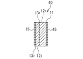
図12は、図11に示した電波吸収衝立40の断面構造の一例を示す断面図である。図12に示した電波吸収衝立40は、2つの面のうちの一方においてのみ、電波吸収機能を有するものである。この電波吸収衝立40は、電波反射体11と、電波反射体11における電波到来側に配置された誘電体層121と、誘電体層121における電波到来側に配置された抵抗層131と、抵抗層131における電波到来側に配置された誘電体層122と、誘電体層122における電波到来側に配置された抵抗層132と、抵抗層132における電波到来側の面を覆う内装材15と、電波反射体11における電波到来側とは反対側の面を覆う内装材45とを備えている。内装材45の材料は内装材15と同様である。なお、内装材15,45の表面に塗装を施してもよい。
【0073】
図13は、図11に示した電波吸収衝立40の断面構造の他の例を示す断面図である。図13に示した電波吸収衝立40は、両面において電波吸収機能を有するものである。この電波吸収衝立40は、図12における電波吸収衝立40と同様の電波反射体11、誘電体層121、抵抗層131、誘電体層122、抵抗層132および内装材15を備えている。図13に示した電波吸収衝立40は、更に、電波反射体11を中心にして、誘電体層121、抵抗層131、誘電体層122、抵抗層132および内装材15と対称に位置に設けられた誘電体層421、抵抗層431、誘電体層422、抵抗層432および内装材45を備えている。この誘電体層421、抵抗層431、誘電体層422、抵抗層432および内装材45の各構成は、それぞれ誘電体層121、抵抗層131、誘電体層122、抵抗層132および内装材15と同様である。
【0074】
なお、電波吸収衝立40の構成は、図12または図13に示した構成に限らず、電波吸収体10と同様に種々の構成を採用することができる。
【0075】
図14、図15はそれぞれ、衝立の芯材に電波吸収パネル60を貼り付けて構成された電波吸収衝立50の設置状態の例を示す断面図である。図14に示した電波吸収衝立50は、板状の芯材51の一方の面に電波吸収パネル60を貼り付けて構成されている。図15に示した電波吸収衝立50は、板状の芯材51の両面にそれぞれ電波吸収パネル60を貼り付けて構成されている。電波吸収パネル60は電波吸収体10を含むパネルである。電波吸収パネル60の構成は、表面に内装材15が配置された電波吸収体10と同様である。また、内装材15の表面に塗装を施してもよい。また、芯材51が金属板である場合には、この芯材51を、電波吸収体10における電波反射体11として兼用してもよい。
【0076】
なお、図14、図15に示した例では、電波吸収衝立50は、下端が床46に固定され、上端が天井47に固定されている。しかし、電波吸収衝立50の下端と床46との間、または電波吸収衝立50の上端と天井47との間が離れていてもよい。また、電波吸収衝立50は、スライディングウォール等のように、可動型の衝立であってもよい。
【0077】
次に、図16を参照して、本実施の形態に係る電波吸収壁について説明する。本実施の形態に係る電波吸収壁は、本実施の形態に係る電波吸収体10を含む壁であって、電波吸収機能を有するものである。図16は、本実施の形態に係る電波吸収壁の構成の一例を示す斜視図である。この電波吸収壁70は、スタッド71、ランナー72および振れ止め73を含む骨組みと、この骨組みに取り付けられた複数の電波吸収パネル60と、この電波吸収パネル60の表面を覆う内装材75とを備えている。
【0078】
次に、図17を参照して、本実施の形態に係る電波吸収天井について説明する。本実施の形態に係る電波吸収天井は、本実施の形態に係る電波吸収体10を含む天井であって、電波吸収機能を有するものである。図17は、本実施の形態に係る電波吸収天井の構成の一例を示す斜視図である。この電波吸収天井80は、野縁81および野縁受け82を含む骨組みと、この骨組みに取り付けられた複数の電波吸収パネル60と、この電波吸収パネル60の表面を覆う内装材85とを備えている。
【0079】
次に、図18を参照して、本実施の形態に係る電波吸収床について説明する。本実施の形態に係る電波吸収床は、本実施の形態に係る電波吸収体10を含む床であって、電波吸収機能を有するものである。図18は、本実施の形態に係る電波吸収床の構成の一例を示す斜視図である。この電波吸収床90は、床板として用いられる複数の電波吸収パネル60と、この電波吸収パネル60を支持する複数の支持脚91と、電波吸収パネル60の表面を覆う内装材95とを備えている。電波吸収パネル60に含まれる誘電体層12として、図7ないし図10に示した例のように、電波の進行方向に貫通する複数の孔を有する板状の部材を用いることにより、電波吸収パネル60は、床板として使用するのに十分な構造強度および耐荷重性を有するようになる。
【0080】
次に、本実施の形態に係る電波吸収体10における電波吸収の原理について説明する。始めに、図1に示したように1組の誘電体層121および抵抗層131を備えた電波吸収体10における電波吸収の原理について説明する。電波反射体と、所定の面抵抗値を有する抵抗皮膜と、これらの間に配置された誘電体とを備えた抵抗皮膜型電波吸収体は、λ/4型電波吸収体の一種であり、広く知られている。この抵抗皮膜型電波吸収体は、電波反射体からλ/4(λは電波の波長)だけ離れた位置において電波反射体側を見込んだ入力インピーダンスが無限大となることに着目して、その位置に、自由空間の特性インピーダンスに等しい面抵抗値377Ω□を有する抵抗皮膜を配置したものである。本実施の形態における抵抗層131に含まれる抵抗膜は上記抵抗皮膜に相当する。また、説明を容易とするために、ここでは抵抗膜用基体の存在を無視して説明する。また、以下の説明において、規格化とは、自由空間の特性インピーダンス(≒377Ω)で規格化したことを意味している。
【0081】
ここで、誘電体の誘電率をεr *(*は複素数であることを表す。)とすると、電波吸収体に電波が垂直に入射する場合、電波反射体からdだけ離れた位置において電波反射体側を見込んだ規格化入力インピーダンスZ*は、次の式で与えられる。なお、“j”は√(−1)を表わす。
【0082】
Z*={1/√(εr *)}・tanh{j・(2πd/λ)・√(εr *)}
【0083】
抵抗皮膜の面抵抗値をRsとすると、抵抗皮膜の前面において電波反射体側を見込んだ規格化入力インピーダンスZin *は、入力インピーダンスZ*の素子と抵抗値Rsの素子が並列に接続された回路の入力インピーダンスと見ることができる。従って、規格化入力インピーダンスZin *は、次の式で与えられる。
【0084】
Zin *={(Rs/377)・Z*}/{(Rs/377)+Z*}
【0085】
ここで、d=λ/{4√(εr *)}の場合には、インピーダンスZ*は無限大となり、インピーダンスZin *は1となる。その結果、抵抗皮膜の表面における反射係数は0になる。
【0086】
次に、図8に示したように2層の誘電体層121,122と1層の抵抗層131と電波吸収性能調整層14とを備えた電波吸収体10、または図7に示したように2層の誘電体層121,122と2層の抵抗層131,132とを備えた電波吸収体10における電波吸収の原理について説明する。
【0087】
この場合の電波吸収体10は、2層型電波吸収体となる。この2層型電波吸収体では、任意の2つの周波数において反射減衰量のピークが存在する電波吸収特性を実現することができる。従って、この2層型電波吸収体によれば、所望の反射減衰量が得られる周波数範囲を広くしたり、2つの周波数帯域において所望の反射減衰量が得られるようにしたりすることができる。2層型電波吸収体の遠方界における理論的設計は、単層型電波吸収体と同様に伝送線理論を用いて行うことができる。
【0088】
以下、抵抗層131内の抵抗膜を第1の抵抗膜と呼び、抵抗層132内の抵抗膜を第2の抵抗膜と呼ぶ。また、第1の抵抗膜の面抵抗値をRs1とし、第2の抵抗膜の面抵抗値をRs2とする。また、誘電体層121の厚さをd1とし、抵抗膜用基体211の厚さをd2とし、誘電体層122の厚さをd4とし、電波吸収性能調整用誘電体層14の厚さをd5とし、抵抗膜用基体212の厚さをd6とする。また、誘電体層121の規格化特性インピーダンスと伝搬定数をそれぞれZc1 *,γ1 *とする。また、抵抗膜用基体211の規格化特性インピーダンスと伝搬定数をそれぞれZc 2 *,γ2 *とする。また、誘電体層122の規格化特性インピーダンスと伝搬定数をそれぞれZc 4 *,γ4 *とする。また、電波吸収性能調整用誘電体層14の規格化特性インピーダンスと伝搬定数をそれぞれZc 5 *,γ5 *とする。また、抵抗膜用基体212の規格化特性インピーダンスと伝搬定数をそれぞれZc 6 *,γ6 *とする。
【0089】
ここで、電波吸収体10に電波が垂直に入射する場合を考える。誘電体層121の電波到来側において電波反射体11側を見込んだ規格化入力インピーダンス(負荷インピーダンス)Z1 *は、次の式で与えられる。
【0090】
Z1 *=Zc1 *・tanhγ1 *d1
【0091】
次に、抵抗膜用基体211の電波到来側において電波反射体11側を見込んだ規格化入力インピーダンスZ2 *は、次の式で与えられる。
【0092】
Z2 *=Zc 2 *・{(Z1 *+Zc 2 *tanhγ2 *d2)/(Zc 2 *+Z1 *tanhγ2 *d2)}
【0093】
次に、第1の抵抗膜の前面において電波反射体11側を見込んだ規格化入力インピーダンスZ3 *は、次の式で与えられる。
【0094】
Z3 *={(Rs1/377)・Z2 *}/{(Rs1/377)+Z2 *}
【0095】
次に、誘電体層122の電波到来側において電波反射体11側を見込んだ規格化入力インピーダンスZ4 *は、次の漸化式で表わされる。
【0096】
Z4 *=Zc 4 *・{(Z3 *+Zc 4 *tanhγ4 *d4)/(Zc 4 *+Z3 *tanhγ4 *d4)}
【0097】
そして、図8における電波吸収性能調整用誘電体層14の電波到来側において電波反射体11側を見込んだ規格化入力インピーダンスZin5 *は、次の漸化式で表わされる。
【0098】
Zin5 *=Zc 5 *・{(Z4 *+Zc 5 *tanhγ5 *d5)/(Zc 5 *+Z4 *tanhγ5 *d5)}
【0099】
また、図7における第2の抵抗膜の前面において電波反射体11側を見込んだ規格化入力インピーダンスZ5 *は、次の式で与えられる。
【0100】
Z5 *={(Rs2/377)・Z4 *}/{(Rs2/377)+Z4 *}
【0101】
そして、図7における抵抗膜用基体212の電波到来側において電波反射体11側を見込んだ規格化入力インピーダンスZin6 *は、次の漸化式で表わされる。
【0102】
Zin6 *=Zc 6 *・{(Z5 *+Zc 6 *tanhγ6 *d6)/(Zc 6 *+Z5 *tanhγ6 *d6)}
【0103】
2層の誘電体層121,122と1層の抵抗層131と電波吸収性能調整用誘電体層14とを備えた電波吸収体10、または2層の誘電体層121,122と2層の抵抗層131,132とを備えた電波吸収体10では、任意の2つの周波数において反射係数を0にする条件が存在する。このような条件を選択して電波吸収体10を設計および製造することにより、任意の2つの周波数において反射減衰量のピークが存在する電波吸収特性を有する電波吸収体10を実現することができる。
【0104】
上記の説明と同様にして、3層以上の誘電体層と、隣り合う誘電体層の間に配置された抵抗層と電波吸収性能調整用誘電体層14とを備えた電波吸収体10や、3層以上の誘電体層と、隣り合う誘電体層の間、および電波反射体11から最も遠い位置に配置された誘電体層における電波到来側に配置された抵抗層とを備えた電波吸収体10についても、電波吸収体10の前面における規格化入力インピーダンスを求めることができる。これらの電波吸収体10では、3つ以上の周波数において反射係数を0にする条件が存在する。このような条件を選択して電波吸収体10を設計および製造することにより、3つ以上の周波数において反射減衰量のピークが存在する電波吸収特性を有する電波吸収体10を実現することができる。
【0105】
次に、本実施の形態に係る電波吸収体10の2つの実施例とそれらの電波吸収特性について説明する。始めに、図19を参照して、実施例の電波吸収体10の電波吸収特性を評価するために用いられる評価システムについて説明する。この評価システムは、反射電力法によって電波吸収体の電波吸収特性を測定するためのものである。反射電力法とは、測定しようとする電波吸収体に電波を放射し、電波吸収体による電波反射量を測定すると共に、測定しようとする電波吸収体と同一面積の反射面を有する金属板についても同様に電波反射量を測定し、これらの電波反射量の比から、電波吸収体の電波吸収特性を測定する方法である。
【0106】
図19に示した評価システムは、評価しようとする試料120に電波を放射する送信アンテナ121と、試料120で反射された電波を受信する受信アンテナ122と、受信アンテナ122に接続されたネットワークアナライザー123と、入力端がネットワークアナライザー123に接続され、出力端が送信アンテナ121に接続された増幅器124とを備えている。図19では、試料120における電波の入射角および出射角をθで表わしている。送信アンテナ121と受信アンテナ122は、アンテナ121,122から試料120における電波の入射位置までの距離が等しくなるように配置される。実施例では、この距離を2mとしている。また、評価システムは、電波暗室125内に設置される。
【0107】
ネットワークアナライザー123は、増幅器124に送信用の信号を送り、この信号は増幅器124によって増幅された後、送信アンテナ121に与えられる。また、ネットワークアナライザー123には、受信アンテナ122によって得られる受信信号が入力される。ネットワークアナライザー123は、送信用の信号と受信信号とに基づいて試料の特性を測定する。
【0108】
[第1の実施例]
第1の実施例の電波吸収体10は、図7に示した構成になっている。第1の実施例の電波吸収体10は、以下のようにして製造した。まず、ロボット塗装装置を用いたスプレー塗装によって、厚さ1mmの板状の抵抗膜用基体211の一方の面の上に導電性塗料を塗布することによって抵抗膜221を形成して、抵抗層131を作製した。抵抗膜221の面抵抗値は350Ω□である。また、同様に、ロボット塗装装置を用いたスプレー塗装によって、厚さ2mmの板状の抵抗膜用基体212の一方の面の上に導電性塗料を塗布することによって抵抗膜222を形成して、抵抗層132を作製した。抵抗膜222の面抵抗値は900Ω□である。次に、鋼板よりなる電波反射体11に、ハニカム形状の誘電体層121を、エポキシ系接着剤を用いて接着した。誘電体層121における1つの孔の径は15mmであり、誘電体層121の厚さは18mmである。次に、抵抗膜221が形成された面を電波到来側の面とし、抵抗膜221が形成された抵抗膜用基体211を、誘電体層121における電波到来側の面に、エポキシ系接着剤を用いて接着した。次に、抵抗膜221に、ハニカム形状の誘電体層122を、エポキシ系接着剤を用いて接着した。誘電体層122における1つの孔の径は15mmであり、誘電体層122の厚さは14mmである。次に、抵抗膜222が形成された面を電波到来側とは反対側の面とし、抵抗膜用基体212上に形成された抵抗膜222を、誘電体層122における電波到来側の面に、エポキシ系接着剤を用いて接着して、電波吸収体10を完成させた。この電波吸収体10の縦および横の寸法は、共に30cmである。
【0109】
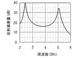
図19に示した評価システムを用い、反射電力法によって、2GHz〜6GHzの周波数範囲における第1の実施例の電波吸収体10の電波吸収特性を測定した。その測定結果を図20に示す。図20から分かるように、第1の実施例の電波吸収体10は、2.4GHzと5.2GHzの各周波数において反射減衰量が20dB以上となる特性を有している。従って、この電波吸収体10は、IEEE802.11bとIEEE802.11aの2つの規格に準拠した2.4GHz帯と5.2GHz帯の2つの周波数帯域における電波障害を防止するために利用することができる。また、現在、規格化が検討されているIEEE802.11gに対応した無線LANシステムにおいても、IEEE802.11bと同じ2.4GHz帯の電波が使用される予定であるため、第1の実施例の電波吸収体10は、このシステムでも利用可能である。
【0110】
図21は、第1の実施例の電波吸収体10について、設計値に基づいて計算によって求めた電波吸収特性と、製造誤差を見込んで計算によって求めた最低限の電波吸収特性とを示している。なお、図21において、符号131は設計値に基づく電波吸収特性を示し、符号132は最低限の電波吸収特性を示している。最低限の電波吸収特性は、誘電体層121,122の厚さと抵抗膜221,222の面抵抗値の製造誤差を見込んで各周波数毎に計算によって求めた最低値の集合である。図21から、第1の実施例の電波吸収体10によれば、製造誤差を見込んでも、2.4GHzと5.2GHzの各周波数において反射減衰量が15dB以上となる特性が得られる可能性があることが確認できた。なお、ここで見込んだ製造誤差は、誘電体層121および誘電体層122の厚さの設計値に対して、それぞれ±1mmおよび±1mm、また、抵抗膜221および抵抗膜222の面抵抗値の設計値に対して、それぞれ±10%および±20%である。
【0111】
[第2の実施例]
第2の実施例の電波吸収体10は、図8に示した構成になっている。第2の実施例の電波吸収体10は、以下のようにして製造した。まず、ロボット塗装装置を用いたスプレー塗装によって、厚さ1mmの板状の抵抗膜用基体211の一方の面の上に導電性塗料を塗布することによって抵抗膜221を形成して、抵抗層131を作製した。抵抗膜221の面抵抗値は250Ω□である。次に、鋼板よりなる電波反射体11に、ハニカム形状の誘電体層121を、エポキシ系接着剤を用いて接着した。誘電体層121における1つの孔の径は15mmであり、誘電体層121の厚さは20mmである。次に、抵抗膜221が形成された面を電波到来側の面とし、抵抗膜221が形成された抵抗膜用基体211を、誘電体層121における電波到来側の面に、エポキシ系接着剤を用いて接着した。次に、抵抗膜221に、ハニカム形状の誘電体層122を、エポキシ系接着剤を用いて接着した。誘電体層122における1つの孔の径は15mmであり、誘電体層122の厚さは6mmである。次に、厚さ6mmの板状の電波吸収特性調整用誘電体層14を、誘電体層122における電波到来側の面に、エポキシ系接着剤を用いて接着して、電波吸収体10を完成させた。この電波吸収体10の縦および横の寸法は、共に30cmである。
【0112】
図19に示した評価システムを用い、反射電力法によって、2GHz〜6GHzの周波数範囲における第2の実施例の電波吸収体10の電波吸収特性を測定した。その測定結果を図22に示す。図22から分かるように、第2の実施例の電波吸収体10は、2.4GHzと5.2GHzの各周波数において反射減衰量が20dB以上となる特性を有している。従って、この電波吸収体10は、IEEE802.11bとIEEE802.11aの2つの規格に準拠した2.4GHz帯と5.2GHz帯の2つの周波数帯域における電波障害を防止するために利用することができる。また、第2の実施例の電波吸収体10は、IEEE802.11gに対応した無線LANシステムでも利用可能である。
【0113】
次に、図23ないし図27を参照して、本実施の形態に係る電波吸収体10によるマルチパス抑制効果について説明する。マルチパスとは、送信部から送信された電波が複数の経路を経て受信部に到達することを言う。室内における無線LANでは、壁面やパーテーション等により電波が反射されやすく、その結果、マルチパスが生じやすい。マルチパスが生じると、基本波と遅延波との合成により信号の劣化が生じたり、複数の経路の電波が干渉して、位置によって受信電力が変動したりする。
【0114】
ここでは、電波吸収体10によるマルチパス抑制効果をシミュレーションによって確認した結果について説明する。図23は、シミュレーションで使用した室内のモデルを示している。この室内のモデルは、幅、長さ、高さが全て2mの立方体形状である。シミュレーションでは、室内の全ての面が金属面であるモデルと、室内の6面のうち、天井面は金属面で、他の5面には電波吸収体10を貼り付けたモデルとを用意した。また、シミュレーションでは、1つの壁から0.3m離れ、この壁の両側の壁から等距離(1m)だけ離れ、床から0.7m離れた位置141に送信アンテナを配置している。送信アンテナは、半波長ダイポールアンテナであり、2.4GHzの垂直偏波の電波を放射する。シミュレーションでは、有限積分法によって、床から0.7m離れた平面142における電界強度分布を求めた。
【0115】
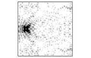
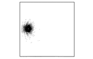
図24は、室内の全ての面が金属面であるモデルにおける電界強度分布を表わしている。図25は、天井面以外の5面に電波吸収体10を貼り付けたモデルにおける電界強度分布を表わしている。図24および図25では、電界強度を濃淡で表わしており、濃い部分ほど電界強度が大きいことを表わしている。図24から、室内の全ての面が金属面であるモデルでは、マルチパスによる電波の干渉が生じていることが分かる。また、図25から、天井面以外の5面に電波吸収体10を貼り付けたモデルでは、マルチパスによる電波の干渉が抑制されていることが分かる。
【0116】
図26は、室内の全ての面が金属面であるモデルについて、平面142内の測定点における電界強度の時間的変化を表わしている。また、測定点は送信アンテナを配置する際に基準とした1つの壁から1m離れ(すなわち、送信アンテナからは0.7m離れ)、この壁の両側の壁から等距離(1m)だけ離れ、床から0.7m離れた点である。図26において、符号151で示した部分は、室内の面で反射していない直接波に対応し、符号152で示した部分は、室内の面で1回反射した反射波に対応する。この反射波の電界強度は、直接波の電界強度に対して3dB程度しか小さくなっていない。また、図26から、このモデルでは、測定点に直接波が到達した後も、電波の多重反射により、長い時間、電界強度が小さくならないことが分かる。
【0117】
図27は、天井面以外の5面に電波吸収体10を貼り付けたモデルについて、平面142内の測定点における電界強度の時間的変化を表わしている。図27において、符号153で示した部分は、室内の面で反射していない直接波に対応し、符号154で示した部分は、室内の面で1回反射した反射波に対応する。この反射波の電界強度は、直接波の電界強度に対して15dB程度小さくなっている。また、図27から、このモデルでは、測定点に直接波が到達した後、短時間で電界強度が小さくなっており、このことからマルチパスの発生が抑制されていることが分かる。
【0118】
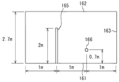
次に、図28ないし図31を参照して、本実施の形態に係る電波吸収体10による電波干渉および電波漏洩の抑制効果について説明する。ここでは、電波吸収体10による電波干渉および電波漏洩の抑制効果をシミュレーションによって確認した結果について説明する。図28はシミュレーションで使用した室内のモデルの平面図、図29はこのモデルの床に垂直な断面を示す断面図である。このモデルは、幅が1m、長さが3m、高さが2.7mの直方体形状である。また、このモデルでは、床面161と、天井面162と、幅が1mの1つの壁面163が金属面で、他の壁面は電波を吸収する面としている。また、このモデルでは、壁163から2m離れた位置において、床面161の上に、高さ2mの衝立165を設置している。シミュレーションでは、衝立165が金属製であるモデルと、衝立165が電波吸収体10を用いたものであるモデルとを用意した。また、シミュレーションでは、壁163から1m離れ、この壁の両側の壁から等距離(0.5m)だけ離れ、床から0.7m離れた位置166に送信アンテナを配置している。送信アンテナは、半波長ダイポールアンテナであり、2.4GHzの垂直偏波の電波を放射する。シミュレーションでは、有限積分法によって、図29に示した断面における電界強度分布を求めた。
【0119】
図30は、衝立165が金属製であるモデルにおける電界強度分布を表わしている。図31は、衝立165が電波吸収体10を用いたものであるモデルにおける電界強度分布を表わしている。図30および図31では、電界強度を濃淡で表わしており、濃い部分ほど電界強度が大きいことを表わしている。図30から、衝立165が金属製であるモデルでは、電波干渉および隣室への電波漏洩が生じていることが分かる。また、図31から、衝立165が電波吸収体10を用いたものであるモデルでは、電波干渉および隣室への電波漏洩が抑制されていることが分かる。
【0120】
以上説明したように、本実施の形態によれば、不燃性を有し且つ軽量で、室内において用いるのに適した電波吸収体、電波吸収パネル、電波吸収衝立、電波吸収壁、電波吸収天井および電波吸収床を実現することができる。また、これらを利用することにより、例えば、室内で構築される無線LANにおける電波干渉や電波漏洩等の電波障害を防止することができる。
【0121】
また、本実施の形態において、電波吸収体の基本構成を、図2ないし図4のいずれかに示した構成とすることにより、少なくとも2つの周波数において反射減衰量のピークが存在する電波吸収特性を実現することができる。これにより、少なくとも2つの周波数帯域における電波障害を防止することが可能になる。特に、電波吸収体の電波吸収特性を、2.4GHzと5.2GHzの各周波数において反射減衰量が15dB以上となる特性とすることにより、2.4GHz帯と5.2GHz帯の少なくとも一方を用いる無線LANにおける電波障害を防止することが可能になる。
【0122】
また、本実施の形態において、誘電体層を、電波の進行方向に貫通する複数の孔を有する板状の部材や板状の発泡体によって形成することにより、電波吸収体をより軽量化することができると共に、電波吸収体に断熱性を持たせることができる。また、誘電体層を、電波の進行方向に貫通する複数の孔を有する板状の部材によって形成することにより、十分な強度を確保することができる。また、誘電体層を、板状の発泡体によって形成することにより、電波吸収体に吸音機能を持たせることができる。
【0123】
また、スプレー塗装を用いて導電性塗料を抵抗膜用基体上に塗布することによって抵抗膜を形成することにより、導電性塗料の塗布方向による電波吸収特性の差が極めて小さい電波吸収体を実現することができる。
【0124】
なお、本発明は、上記実施の形態に限定されず、種々の変更が可能である。例えば、電波吸収体10を構成する各層の材料は、実施の形態に示したものに限らず、適宜選択することができる。
【0125】
【発明の効果】
以上説明したように、請求項1ないし18のいずれかに記載の電波吸収体、請求項19記載の電波吸収パネル、請求項20記載の電波吸収衝立、請求項21記載の電波吸収壁、請求項22記載の電波吸収天井または請求項23記載の電波吸収床によれば、不燃性を有し且つ軽量で、室内において用いるのに適した電波吸収体、電波吸収パネル、電波吸収衝立、電波吸収壁、電波吸収天井または電波吸収床を実現することができるという効果を奏する。
【0126】
また、請求項2または5記載の電波吸収体、もしくは請求項2または5を引用する請求項のいずれかに記載の電波吸収体、電波吸収パネル、電波吸収衝立、電波吸収壁、電波吸収天井または電波吸収床によれば、少なくとも2つの周波数帯域における電波障害を防止することが可能になるという効果を奏する。
【0127】
また、請求項13または14記載の電波吸収体、もしくは請求項13または14を引用する請求項のいずれかに記載の電波吸収体、電波吸収パネル、電波吸収衝立、電波吸収壁、電波吸収天井または電波吸収床によれば、電波吸収体をより軽量化することができると共に、電波吸収体に断熱性を持たせることができるという効果を奏する。
【図面の簡単な説明】
【図1】本発明の一実施の形態に係る電波吸収体の基本構成の第1の例を示す断面図である。
【図2】本発明の一実施の形態に係る電波吸収体の基本構成の第2の例を示す断面図である。
【図3】本発明の一実施の形態に係る電波吸収体の基本構成の第3の例を示す断面図である。
【図4】本発明の一実施の形態に係る電波吸収体の基本構成の第4の例を示す断面図である。
【図5】本発明の一実施の形態に係る電波吸収体の構成の他の例を示す断面図である。
【図6】本発明の一実施の形態における抵抗層の形成方法を示す説明図である。
【図7】複数の孔を有する板状の部材によって形成された誘電体層を有する電波吸収体の構成の第1の例を示す斜視図である。
【図8】複数の孔を有する板状の部材によって形成された誘電体層を有する電波吸収体の構成の第2の例を示す斜視図である。
【図9】複数の孔を有する板状の部材によって形成された誘電体層を有する電波吸収体の構成の第3の例を示す斜視図である。
【図10】複数の孔を有する板状の部材によって形成された誘電体層を有する電波吸収体の構成の第4の例を示す斜視図である。
【図11】電波吸収体によって主要部分が構成された電波吸収衝立の設置状態の一例を示す断面図である。
【図12】図11に示した電波吸収衝立の断面構造の一例を示す断面図である。
【図13】図11に示した電波吸収衝立の断面構造の他の例を示す断面図である。
【図14】衝立の芯材に電波吸収パネルを貼り付けて構成された電波吸収衝立の設置状態の一例を示す断面図である。
【図15】衝立の芯材に電波吸収パネルを貼り付けて構成された電波吸収衝立の設置状態の他の例を示す断面図である。
【図16】本発明の一実施の形態に係る電波吸収壁の構成の一例を示す斜視図である。
【図17】本発明の一実施の形態に係る電波吸収天井の構成の一例を示す斜視図である。
【図18】本発明の一実施の形態に係る電波吸収床の構成の一例を示す斜視図である。
【図19】本発明の一実施の形態における実施例の電波吸収体の電波吸収特性を評価するために用いられる評価システムを示す説明図である。
【図20】本発明の一実施の形態における第1の実施例の電波吸収体の電波吸収特性を示す特性図である。
【図21】本発明の一実施の形態における第1の実施例の電波吸収体について、設計値に基づいて計算によって求めた電波吸収特性と製造誤差を見込んで計算によって求めた最低限の電波吸収特性とを示す特性図である。
【図22】本発明の一実施の形態における第2の実施例の電波吸収体の電波吸収特性を示す特性図である。
【図23】本発明の一実施の形態に係る電波吸収体によるマルチパス抑制効果を確認するためのシミュレーションで使用した室内のモデルを示す斜視図である。
【図24】本発明の一実施の形態に係る電波吸収体によるマルチパス抑制効果を確認するためのシミュレーションの結果を示す説明図である。
【図25】本発明の一実施の形態に係る電波吸収体によるマルチパス抑制効果を確認するためのシミュレーションの結果を示す説明図である。
【図26】本発明の一実施の形態に係る電波吸収体によるマルチパス抑制効果を確認するためのシミュレーションの結果を示す特性図である。
【図27】本発明の一実施の形態に係る電波吸収体によるマルチパス抑制効果を確認するためのシミュレーションの結果を示す特性図である。
【図28】本発明の一実施の形態に係る電波吸収体による電波干渉および電波漏洩の抑制効果を確認するためのシミュレーションで使用した室内のモデルを示す平面図である。
【図29】図28に示したモデルの断面図である。
【図30】本発明の一実施の形態に係る電波吸収体による電波干渉および電波漏洩の抑制効果を確認するためのシミュレーションの結果を示す説明図である。
【図31】本発明の一実施の形態に係る電波吸収体による電波干渉および電波漏洩の抑制効果を確認するためのシミュレーションの結果を示す説明図である。
【符号の説明】
10…電波吸収体、11…電波反射体、12,121,122…誘電体層、13,131,132…抵抗層、14…電波吸収特性調整用誘電体層、211,221…抵抗膜用基体、212,222…抵抗膜。[0001]
TECHNICAL FIELD OF THE INVENTION
The present invention relates to a radio wave absorber, a radio wave absorption panel, a radio wave absorption screen, and a radio wave absorption device which can be used to prevent radio interference such as radio wave interference and radio wave leakage in a wireless LAN (local area network) constructed indoors. The present invention relates to a wall, a radio wave absorbing ceiling, and a radio wave absorbing floor.
[0002]
[Prior art]
2. Description of the Related Art In recent years, wireless LANs have been attracting attention as network construction technologies in rooms such as offices and homes. However, when constructing a wireless LAN indoors, there is a problem that radio interference such as radio interference and radio leakage is likely to occur. For example, when radio waves used for communication are reflected multiple times due to a wall surface, a partition, or the like, a reduction in data transfer rate, deterioration of a communication signal such as mixing of noise, and interference with other communication devices occur. Also, for example, even if it is desired to provide a plurality of base stations in the office, if the frequency of the radio waves used by the plurality of base stations is the same, radio wave interference occurs between the plurality of base stations, The desired number of lines cannot be secured. Therefore, as one of EMC (Electromagnetic Compatibility) techniques for preventing such a radio wave interference, it is considered that a wall surface or a partition in a room has radio wave absorption performance.
[0003]
For example, Patent Literature 1 describes a non-combustible electromagnetic wave absorbing wall material for an interior. The wall material includes an inorganic radio wave absorbing plate and a radio wave reflector provided on one surface of the inorganic radio wave absorbing plate. The inorganic radio wave absorption plate is made of cement, silica raw material, fiber reinforcing material and ferrite powder having a content of 50 to 70% by weight.
[0004]
Non-Patent Document 1 discloses a λ / 4 type radio wave absorber formed by bonding a resistive film to a gypsum board. In this radio wave absorber, the resistive film is formed by applying a conductive paint to a PET (polyethylene terephthalate) film.
[0005]
[Patent Document 1]
JP-A-2002-364154
[Non-patent document 1]
Proceedings of CMC Technical Seminar “Latest Technology Trends of Electromagnetic Wave Absorbers”, CMC Publishing Co., Ltd., November 18, 2002, pp. 81-82
[0006]
[Problems to be solved by the invention]
The incombustible electric wave absorbing wall material for interior described in Patent Literature 1 is unlikely to be a lightweight wall material in view of its raw materials. Therefore, it is difficult to say that this non-flammable radio wave absorbing wall material for interior is suitable as a wall material for interior. Further, the radio wave absorption characteristics of the non-combustible radio wave absorbing wall material for interior described in Patent Literature 1 have a peak of reflection loss only at a frequency of 2.4 GHz. However, currently, in a wireless LAN, two frequency bands based on two standards of IEEE802.11b and IEEE802.11a, that is, 2.4 GHz band and 5.2 GHz band are used. Therefore, the non-combustible radio wave absorbing wall material for interior described in Patent Literature 1 has a problem that even if radio wave interference in the 2.4 GHz band can be prevented, radio wave interference in the 5.2 GHz band cannot be prevented. In addition, the 2.4 GHz band based on IEEE802.11b is 2.4 GHz to 2.497 GHz in Japan. In addition, the 5.2 GHz band based on IEEE802.11a is 5.15 GHz to 5.25 GHz in Japan.
[0007]
In the radio wave absorber described in Non-Patent Document 1, the resistive film is formed by applying a conductive paint to a PET film. Therefore, this radio wave absorber is not nonflammable and is not suitable for use in indoor walls. In addition, this radio wave absorber has a problem that the radio wave absorption characteristics change depending on the application direction of the conductive paint. Further, the radio wave absorption characteristics of this radio wave absorber have a reflection loss peak only at one frequency. For this reason, this radio wave absorber has a problem that it is impossible to prevent radio interference in both of the two frequency bands used in the wireless LAN.
[0008]
The present invention has been made in view of the above problems, and a first object of the present invention is to provide a radio wave absorber, a radio wave absorption panel, a radio wave absorption panel, a radio wave absorption screen, a non-flammable, lightweight, and suitable for indoor use. It is an object of the present invention to provide an absorbing wall, a radio wave absorbing ceiling and a radio wave absorbing floor.
[0009]
Further, a second object of the present invention, in addition to the first object, is a radio wave absorber, a radio wave absorption panel, a radio wave absorption screen, a radio wave absorption wall, a radio wave absorber which can prevent radio interference in at least two frequency bands. It is an object of the present invention to provide an absorbing ceiling and a radio wave absorbing floor.
[0010]
[Means for Solving the Problems]
The first radio wave absorber of the present invention is:
A non-flammable radio wave reflector,
A non-combustible dielectric layer mainly composed of an inorganic material and arranged on the radio wave arrival side of the radio wave reflector,
A plate-shaped or sheet-shaped resistive film base mainly made of an inorganic material, and including a resistive film formed on the resistive film base, including a resistive layer disposed on the radio wave arrival side of the dielectric layer,
The whole is non-flammable.
[0011]
The second radio wave absorber of the present invention comprises:
A non-flammable radio wave reflector,
An n-layer (n is an integer of 2 or more) non-combustible dielectric layer mainly composed of an inorganic material and disposed on the radio wave arrival side of the radio wave reflector;
Including a plate-shaped or sheet-shaped substrate for a resistance film mainly made of an inorganic material and a resistance film formed on the substrate for a resistance film, the substrate is disposed between two adjacent dielectric layers (n-1). ) Layer of resistance layer,
Mainly composed of an inorganic material, comprising a dielectric layer for radio wave absorption characteristic adjustment arranged on the radio wave arrival side in the dielectric layer farthest from the radio wave reflector,
The whole is non-flammable.
[0012]
The second radio wave absorber of the present invention may have a characteristic that the return loss is 15 dB or more at a plurality of frequencies. Further, the second radio wave absorber of the present invention may have a characteristic that the return loss is 15 dB or more at each of 2.4 GHz and 5.2 GHz.
[0013]
The third radio wave absorber of the present invention is:
A non-flammable radio wave reflector,
An n-layer (n is an integer of 2 or more) non-combustible dielectric layer mainly composed of an inorganic material and disposed on the radio wave arrival side of the radio wave reflector;
Including a plate-shaped or sheet-shaped resistive film base mainly composed of an inorganic material, and a resistive film formed on the resistive film base, between two adjacent dielectric layers and farthest from a radio wave reflector An n-layer resistive layer disposed on the radio wave arrival side of the dielectric layer,
The whole is non-flammable.
[0014]
In the third radio wave absorber of the present invention, the closer the resistance film is to the radio wave reflector, the smaller the sheet resistance may be. Further, the third radio wave absorber of the present invention may have a characteristic that the return loss is 15 dB or more at a plurality of frequencies. Further, the third radio wave absorber of the present invention may have a characteristic that the return loss is 15 dB or more at each frequency of 2.4 GHz and 5.2 GHz.
[0015]
In the first to third radio wave absorbers of the present invention, the resistive film may be formed on the surface on the radio wave arrival side of the resistive film base, or may be formed on the opposite surface. Good.
[0016]
Further, in the present application, "non-flammable" means having a non-flammable performance compatible with a non-flammable material specified in the Building Standards Law, and a non-flammable performance equivalent to the non-flammable performance of a non-flammable material specified in the Building Standards Law To have.
[0017]
The first to third radio wave absorbers of the present invention may further include an interior material arranged so as to cover a surface farthest from the radio wave reflector. In the first to third radio wave absorbers of the present invention, a surface farthest from the radio wave reflector may be coated.
[0018]
In the first to third radio wave absorbers of the present invention, the radio wave reflector is a plate-shaped radio wave reflector base mainly composed of an inorganic material, and a radio wave reflector base on a radio wave arrival side surface. And a conductive film disposed thereon. Further, the radio wave reflector may be bonded to the dielectric layer with an inorganic adhesive or an organic adhesive.
[0019]
Further, in the first to third radio wave absorbers of the present invention, the dielectric layer may be formed of a plate-shaped member having a plurality of holes penetrating in the traveling direction of radio waves, or a plate-shaped foam. Good. In this case, the dielectric layer has a first surface on the radio wave arrival side and a second surface on the opposite side, and at least the first surface of the first surface and the second surface is It may be covered by a plate-shaped or sheet-shaped member mainly made of an inorganic material.
[0020]
In the first to third radio wave absorbers of the present invention, the resistive film may be formed of a conductive material mixed with a coating agent and may be formed of a conductive paint applied on a resistive film base. Good. In this case, the coating agent may include at least one of an inorganic coating agent and an organic coating agent. Further, the conductive material may include at least one of carbon powder, carbon fiber, metal powder, and metal fiber.
[0021]
In the first to third radio wave absorbers of the present invention, the resistance layer may be bonded to the dielectric layer with an inorganic adhesive or an organic adhesive.
[0022]
Further, the radio wave absorbing panel of the present invention is a panel including any one of the first to third radio wave absorbers of the present invention, which is used as at least a part of any of a screen, a wall, a ceiling, and a floor. It is.
[0023]
The radio wave absorption screen of the present invention is a screen including any one of the first to third radio wave absorbers of the present invention, and has a radio wave absorbing function.
[0024]
Further, the radio wave absorbing wall of the present invention is a wall including any of the first to third radio wave absorbers of the present invention, and has a radio wave absorbing function.
[0025]
Further, the radio wave absorbing ceiling of the present invention is a ceiling including any one of the first to third radio wave absorbers of the present invention, and has a radio wave absorbing function.
[0026]
Further, the radio wave absorption floor of the present invention is a floor including the radio wave absorber of any of the first to third aspects of the present invention, and has a radio wave absorbing function.
[0027]
BEST MODE FOR CARRYING OUT THE INVENTION
Hereinafter, an embodiment of the present invention will be described in detail with reference to the drawings. First, the configuration of the radio wave absorber according to the present embodiment will be described with reference to FIGS. 1 to 4 are cross-sectional views showing first to fourth examples of the basic configuration of the radio wave absorber according to the present embodiment. Note that, in FIGS. 1 to 4, the arrow denoted by reference numeral 1 indicates the traveling direction of the radio wave.
[0028]
The
[0029]
The
[0030]
The
[0031]
A
[0032]
The
[0033]
The configuration of the
[0034]
Hereinafter, each dielectric layer in FIGS. 1 to 4 will be referred to as a
[0035]
In the
[0036]
The radio wave absorption characteristic of the
[0037]
The
[0038]
In the
[0039]
The
[0040]
Further, as shown in FIG. 5,
[0041]
The
[0042]
In the
[0043]
Next, a method for forming the
[0044]
The
[0045]
As shown in FIG. 6, as a method of applying the
[0046]
The inorganic coating agent used for the
[0047]
The organic coating agent used for the
[0048]
Further, as a coating agent used for the
[0049]
Further, in the case where the
[0050]
Here, an example of a method for manufacturing the
[0051]
The fact that the
[0052]
The
[0053]
The material and manufacturing method of the
[0054]
The inorganic adhesive is not particularly limited, and those conventionally used as nonflammable inorganic adhesives can be used. As the inorganic adhesive, for example, an aluminum phosphate solution, colloidal silica, colloidal alumina, or the like, a curing agent, a water-soluble or water-dispersed inorganic adhesive formed by mixing a catalyst, or the like can be used. .
[0055]
When the
[0056]
Next, the
[0057]
The
[0058]
The
[0059]
The
[0060]
The
[0061]
As shown in FIGS. 7 to 10, by using a plate-like member having a plurality of holes penetrating in the traveling direction of the radio wave as the
[0062]
The honeycomb-shaped, corrugated-shaped or lattice-shaped
[0063]
When the
[0064]
When the
[0065]
The fact that the
[0066]
Next, the
[0067]
When bonding the metal foil to the radio wave reflector base, for example, an inorganic adhesive or an organic adhesive is used. When an organic adhesive is used, the adhesive layer needs to be thin so that the non-combustibility of the
[0068]
The conductive paint may be an organic paint, but is preferably an inorganic paint. When an organic conductive paint is used, it is necessary to reduce the thickness of the conductive paint applied so that the non-flammability of the
[0069]
The
[0070]
Next, a radio wave absorption partition according to the present embodiment will be described with reference to FIGS. The radio wave absorbing screen according to the present embodiment is a screen including the
[0071]
FIG. 11 is a cross-sectional view illustrating an example of an installation state of the radio
[0072]
FIG. 12 is a cross-sectional view showing an example of a cross-sectional structure of the radio
[0073]
FIG. 13 is a cross-sectional view showing another example of the cross-sectional structure of the radio
[0074]
The configuration of the radio
[0075]
14 and 15 are cross-sectional views each showing an example of an installation state of a radio
[0076]
In the examples shown in FIGS. 14 and 15, the lower end of the radio
[0077]
Next, a radio wave absorbing wall according to the present embodiment will be described with reference to FIG. The radio wave absorbing wall according to the present embodiment is a wall including the
[0078]
Next, a radio wave absorbing ceiling according to the present embodiment will be described with reference to FIG. The radio wave absorbing ceiling according to the present embodiment is a ceiling including the
[0079]
Next, a radio wave absorbing floor according to the present embodiment will be described with reference to FIG. The radio wave absorbing floor according to the present embodiment is a floor including the
[0080]
Next, the principle of radio wave absorption in
[0081]
Here, the dielectric constant of the dielectric is εr *(* Denotes a complex number.) When a radio wave is vertically incident on the radio wave absorber, the normalized input impedance Z that looks into the radio wave reflector side at a position distant from the radio wave reflector by d.*Is given by the following equation: Note that “j” represents −1 (−1).
[0082]
Z*= {1 / √ (εr *)} · Tanh {j · (2πd / λ) · √ (εr *)}
[0083]
Assuming that the sheet resistance value of the resistive film is Rs, a normalized input impedance Z that allows for the radio wave reflector side in front of the resistive filmin *Is the input impedance Z*Can be regarded as the input impedance of a circuit in which the element having the resistance value Rs and the element having the resistance value Rs are connected in parallel. Therefore, the normalized input impedance Zin *Is given by the following equation:
[0084]
Zin *= {(Rs / 377) · Z*} / {(Rs / 377) + Z*}
[0085]
Here, d = λ / {4} (εr *) In case of}, impedance Z*Becomes infinite and the impedance Zin *Becomes 1. As a result, the reflection coefficient on the surface of the resistance film becomes zero.
[0086]
Next, as shown in FIG.1, 122And one
[0087]
In this case, the
[0088]
Hereinafter, the
[0089]
Here, a case is considered where a radio wave is vertically incident on the
[0090]
Z1 *= Zc1 *・ Tanhγ1 *d1
[0091]
Next, the
[0092]
Z2 *= Zc 2 *・ {(Z1 *+ Zc 2 *tanhγ2 *d2) / (Zc 2 *+ Z1 *tanhγ2 *d2)}
[0093]
Next, on the front surface of the first resistance film, the normalized input impedance Z3 *Is given by the following equation:
[0094]
Z3 *= {(Rs1 / 377) · Z2 *} / {(Rs1 / 377) + Z2 *}
[0095]
Next, the
[0096]
Z4 *= Zc 4 *・ {(Z3 *+ Zc 4 *tanhγ4 *d4) / (Zc 4 *+ Z3 *tanhγ4 *d4)}
[0097]
Then, on the radio wave arrival side of the radio wave absorption performance adjusting
[0098]
Zin5 *= Zc 5 *・ {(Z4 *+ Zc 5 *tanhγ5 *d5) / (Zc 5 *+ Z4 *tanhγ5 *d5)}
[0099]
Further, a normalized input impedance Z in which the
[0100]
Z5 *= {(Rs2 / 377) · Z4 *} / {(Rs2 / 377) + Z4 *}
[0101]
Then, the
[0102]
Zin6 *= Zc 6 *・ {(Z5 *+ Zc 6 *tanhγ6 *d6) / (Zc 6 *+ Z5 *tanhγ6 *d6)}
[0103]
Two
[0104]
Similarly to the above description, a
[0105]
Next, two examples of the
[0106]
The evaluation system shown in FIG. 19 includes a transmitting
[0107]
The
[0108]
[First Embodiment]
The
[0109]
Using the evaluation system shown in FIG. 19, the radio wave absorption characteristics of the
[0110]
FIG. 21 shows the radio wave absorption characteristics of the
[0111]
[Second embodiment]
The
[0112]
Using the evaluation system shown in FIG. 19, the radio wave absorption characteristics of the
[0113]
Next, with reference to FIG. 23 to FIG. 27, the multipath suppression effect of the
[0114]
Here, the result of confirming the multipath suppression effect of the
[0115]
FIG. 24 illustrates an electric field intensity distribution in a model in which all surfaces in the room are metal surfaces. FIG. 25 illustrates an electric field intensity distribution in a model in which the
[0116]
FIG. 26 shows a temporal change of the electric field intensity at a measurement point in the
[0117]
FIG. 27 illustrates a temporal change of the electric field intensity at a measurement point in the
[0118]
Next, with reference to FIG. 28 to FIG. 31, the effect of suppressing radio wave interference and radio wave leakage by the
[0119]
FIG. 30 shows an electric field intensity distribution in a model in which the
[0120]
As described above, according to the present embodiment, a radio wave absorber, a radio wave absorption panel, a radio wave absorption screen, a radio wave absorption wall, a radio wave absorption ceiling, and a non-flammable and lightweight, suitable for indoor use A radio wave absorbing floor can be realized. Further, by using these, it is possible to prevent radio interference such as radio wave interference and radio wave leakage in a wireless LAN constructed indoors, for example.
[0121]
Further, in the present embodiment, by adopting the basic configuration of the radio wave absorber shown in any one of FIGS. 2 to 4, the radio wave absorption characteristic having the peak of the return loss at at least two frequencies is improved. Can be realized. This makes it possible to prevent radio interference in at least two frequency bands. In particular, at least one of the 2.4 GHz band and the 5.2 GHz band is used by setting the radio wave absorption characteristics of the radio wave absorber so that the return loss is 15 dB or more at each frequency of 2.4 GHz and 5.2 GHz. Radio interference in a wireless LAN can be prevented.
[0122]
Further, in the present embodiment, the weight of the radio wave absorber can be further reduced by forming the dielectric layer by a plate-shaped member or a plate-shaped foam having a plurality of holes penetrating in the traveling direction of radio waves. In addition to this, the radio wave absorber can be provided with heat insulation. Further, by forming the dielectric layer by a plate-shaped member having a plurality of holes penetrating in the traveling direction of radio waves, sufficient strength can be ensured. Further, by forming the dielectric layer with a plate-like foam, the radio wave absorber can have a sound absorbing function.
[0123]
In addition, by forming a resistive film by applying a conductive paint on the resistive film substrate using spray coating, a radio wave absorber having a very small difference in radio wave absorption characteristics depending on the application direction of the conductive paint is realized. be able to.
[0124]
It should be noted that the present invention is not limited to the above embodiment, and various modifications are possible. For example, the material of each layer constituting the
[0125]
【The invention's effect】
As explained above, the radio wave absorber according to any one of claims 1 to 18, the radio wave absorption panel according to claim 19, the radio wave absorption screen according to
[0126]
Also, the radio wave absorber according to
[0127]
Also, the radio wave absorber according to claim 13 or 14, or the radio wave absorber, radio wave absorption panel, radio wave absorption screen, radio wave absorption wall, radio wave absorption ceiling, or the radio wave absorber according to any one of
[Brief description of the drawings]
FIG. 1 is a cross-sectional view showing a first example of a basic configuration of a radio wave absorber according to an embodiment of the present invention.
FIG. 2 is a cross-sectional view showing a second example of the basic configuration of the radio wave absorber according to one embodiment of the present invention.
FIG. 3 is a sectional view showing a third example of the basic configuration of the radio wave absorber according to one embodiment of the present invention.
FIG. 4 is a sectional view showing a fourth example of the basic configuration of the radio wave absorber according to one embodiment of the present invention.
FIG. 5 is a cross-sectional view showing another example of the configuration of the radio wave absorber according to one embodiment of the present invention.
FIG. 6 is an explanatory diagram illustrating a method for forming a resistance layer according to an embodiment of the present invention.
FIG. 7 is a perspective view showing a first example of a configuration of a radio wave absorber having a dielectric layer formed by a plate-shaped member having a plurality of holes.
FIG. 8 is a perspective view showing a second example of the configuration of a radio wave absorber having a dielectric layer formed by a plate-shaped member having a plurality of holes.
FIG. 9 is a perspective view showing a third example of a configuration of a radio wave absorber having a dielectric layer formed by a plate-like member having a plurality of holes.
FIG. 10 is a perspective view showing a fourth example of the configuration of a radio wave absorber having a dielectric layer formed by a plate-like member having a plurality of holes.
FIG. 11 is a cross-sectional view showing an example of an installation state of a radio wave absorbing partition whose main part is constituted by a radio wave absorber.
12 is a sectional view showing an example of a sectional structure of the radio wave absorbing screen shown in FIG.
13 is a sectional view showing another example of the sectional structure of the radio wave absorbing screen shown in FIG.
FIG. 14 is a cross-sectional view illustrating an example of an installation state of a radio wave absorbing screen configured by attaching a radio wave absorbing panel to a core of the screen.
FIG. 15 is a cross-sectional view showing another example of an installation state of a radio wave absorbing screen configured by attaching a radio wave absorbing panel to a core material of the screen.
FIG. 16 is a perspective view showing an example of a configuration of a radio wave absorbing wall according to one embodiment of the present invention.
FIG. 17 is a perspective view showing an example of a configuration of a radio wave absorbing ceiling according to one embodiment of the present invention.
FIG. 18 is a perspective view showing an example of a configuration of a radio wave absorption floor according to one embodiment of the present invention.
FIG. 19 is an explanatory diagram showing an evaluation system used for evaluating the radio wave absorption characteristics of the radio wave absorber of the example in one embodiment of the present invention.
FIG. 20 is a characteristic diagram showing a radio wave absorption characteristic of the radio wave absorber of the first example in one embodiment of the present invention.
FIG. 21 is a graph showing the minimum radio wave absorption obtained by calculation in consideration of the radio wave absorption characteristic and the manufacturing error calculated based on the design value for the radio wave absorber of the first example of the embodiment of the present invention; It is a characteristic view which shows a characteristic.
FIG. 22 is a characteristic diagram showing a radio wave absorption characteristic of the radio wave absorber of the second example in one embodiment of the present invention.
FIG. 23 is a perspective view showing an indoor model used in a simulation for confirming a multipath suppression effect of the radio wave absorber according to one embodiment of the present invention.
FIG. 24 is an explanatory diagram showing a result of a simulation for confirming a multipath suppression effect by the radio wave absorber according to one embodiment of the present invention.
FIG. 25 is an explanatory diagram showing a result of a simulation for confirming a multipath suppression effect by the radio wave absorber according to one embodiment of the present invention.
FIG. 26 is a characteristic diagram showing a result of a simulation for confirming a multipath suppressing effect by the radio wave absorber according to one embodiment of the present invention.
FIG. 27 is a characteristic diagram showing a result of a simulation for confirming a multipath suppression effect by the radio wave absorber according to one embodiment of the present invention.
FIG. 28 is a plan view showing a model of a room used in a simulation for confirming an effect of suppressing radio wave interference and radio wave leakage by the radio wave absorber according to one embodiment of the present invention.
FIG. 29 is a sectional view of the model shown in FIG. 28;
FIG. 30 is an explanatory diagram showing the results of a simulation for confirming the effect of suppressing the radio wave interference and the radio wave leakage by the radio wave absorber according to one embodiment of the present invention.
FIG. 31 is an explanatory diagram showing the results of a simulation for confirming the effect of suppressing the radio wave interference and the radio wave leakage by the radio wave absorber according to one embodiment of the present invention.
[Explanation of symbols]
10 ... radio wave absorber, 11 ... radio wave reflector, 12, 121, 122...
Claims (23)
主に無機材料からなり、前記電波反射体における電波到来側に配置された不燃性の誘電体層と、
主に無機材料からなる板状またはシート状の抵抗膜用基体、およびこの抵抗膜用基体上に形成された抵抗膜を含み、前記誘電体層における電波到来側に配置された抵抗層とを備え、
全体が不燃性であることを特徴とする電波吸収体。A non-flammable radio wave reflector,
A non-combustible dielectric layer mainly composed of an inorganic material and disposed on a radio wave arrival side of the radio wave reflector,
A plate- or sheet-shaped resistive film base mainly composed of an inorganic material, and a resistive layer including a resistive film formed on the resistive film base and disposed on the radio wave arrival side of the dielectric layer. ,
A radio wave absorber characterized in that the whole is nonflammable.
主に無機材料からなり、前記電波反射体における電波到来側に配置されたn層(nは2以上の整数)の不燃性の誘電体層と、
主に無機材料からなる板状またはシート状の抵抗膜用基体、およびこの抵抗膜用基体上に形成された抵抗膜を含み、隣り合う2つの誘電体層の間に配置された(n−1)層の抵抗層と、
主に無機材料からなり、前記電波反射体から最も遠い誘電体層における電波到来側に配置された電波吸収特性調整用誘電体層とを備え、
全体が不燃性であることを特徴とする電波吸収体。A non-flammable radio wave reflector,
An n-layer (n is an integer of 2 or more) non-combustible dielectric layer mainly composed of an inorganic material and disposed on a radio wave arrival side of the radio wave reflector;
Including a plate-shaped or sheet-shaped substrate for a resistance film mainly composed of an inorganic material and a resistance film formed on the substrate for a resistance film, the substrate is disposed between two adjacent dielectric layers (n-1). ) Layer of resistance layer,
Mainly composed of an inorganic material, comprising a dielectric layer for adjusting radio wave absorption characteristics arranged on the radio wave arrival side of the dielectric layer farthest from the radio wave reflector,
A radio wave absorber characterized in that the whole is nonflammable.
主に無機材料からなり、前記電波反射体における電波到来側に配置されたn層(nは2以上の整数)の不燃性の誘電体層と、
主に無機材料からなる板状またはシート状の抵抗膜用基体、およびこの抵抗膜用基体上に形成された抵抗膜を含み、隣り合う2つの誘電体層の間、および前記電波反射体から最も遠い誘電体層における電波到来側に配置されたn層の抵抗層とを備え、
全体が不燃性であることを特徴とする電波吸収体。A non-flammable radio wave reflector,
An n-layer (n is an integer of 2 or more) non-combustible dielectric layer mainly composed of an inorganic material and disposed on a radio wave arrival side of the radio wave reflector;
Including a plate-shaped or sheet-shaped substrate for a resistance film mainly composed of an inorganic material, and a resistance film formed on the substrate for a resistance film, between the two adjacent dielectric layers and the most from the radio wave reflector. An n-layer resistance layer disposed on the radio wave arrival side of the far dielectric layer,
A radio wave absorber characterized in that the whole is nonflammable.
Priority Applications (1)
| Application Number | Priority Date | Filing Date | Title |
|---|---|---|---|
| JP2003057979A JP2004270143A (en) | 2003-03-05 | 2003-03-05 | Radio wave absorber, radio wave absorbing panel, radio wave absorbing screen, radio wave absorbing wall, radio wave absorbing ceiling, and radio wave absorbing floor |
Applications Claiming Priority (1)
| Application Number | Priority Date | Filing Date | Title |
|---|---|---|---|
| JP2003057979A JP2004270143A (en) | 2003-03-05 | 2003-03-05 | Radio wave absorber, radio wave absorbing panel, radio wave absorbing screen, radio wave absorbing wall, radio wave absorbing ceiling, and radio wave absorbing floor |
Publications (1)
| Publication Number | Publication Date |
|---|---|
| JP2004270143A true JP2004270143A (en) | 2004-09-30 |
Family
ID=33121202
Family Applications (1)
| Application Number | Title | Priority Date | Filing Date |
|---|---|---|---|
| JP2003057979A Pending JP2004270143A (en) | 2003-03-05 | 2003-03-05 | Radio wave absorber, radio wave absorbing panel, radio wave absorbing screen, radio wave absorbing wall, radio wave absorbing ceiling, and radio wave absorbing floor |
Country Status (1)
| Country | Link |
|---|---|
| JP (1) | JP2004270143A (en) |
Cited By (15)
| Publication number | Priority date | Publication date | Assignee | Title |
|---|---|---|---|---|
| JP2006339592A (en) * | 2005-06-06 | 2006-12-14 | Yokohama Rubber Co Ltd:The | Electromagnetic wave absorbing building material |
| WO2007034869A1 (en) * | 2005-09-26 | 2007-03-29 | Matsushita Electric Industrial Co., Ltd. | Electronic device containing case, electromagnetic shield body, and electronic device containing structure |
| CN110626017A (en) * | 2018-06-21 | 2019-12-31 | 加川清二 | Electromagnetic wave absorption composite board |
| JP2020145278A (en) * | 2019-03-05 | 2020-09-10 | 出光興産株式会社 | Electromagnetic wave absorption sheet and manufacturing method of the same |
| EP3806598A4 (en) * | 2019-06-07 | 2022-03-09 | Nitto Denko Corporation | Radio wave absorbing member, radio wave absorbing structure, and inspection device |
| WO2023076405A1 (en) * | 2021-10-26 | 2023-05-04 | Pivotal Commware, Inc. | Rf absorbing structures |
| US11757180B2 (en) | 2019-02-20 | 2023-09-12 | Pivotal Commware, Inc. | Switchable patch antenna |
| US11843955B2 (en) | 2021-01-15 | 2023-12-12 | Pivotal Commware, Inc. | Installation of repeaters for a millimeter wave communications network |
| US11844050B2 (en) | 2020-09-08 | 2023-12-12 | Pivotal Commware, Inc. | Installation and activation of RF communication devices for wireless networks |
| US11848478B2 (en) | 2019-02-05 | 2023-12-19 | Pivotal Commware, Inc. | Thermal compensation for a holographic beam forming antenna |
| JP7445912B2 (en) | 2019-08-29 | 2024-03-08 | 国立大学法人 名古屋工業大学 | radio wave absorber |
| US11929822B2 (en) | 2021-07-07 | 2024-03-12 | Pivotal Commware, Inc. | Multipath repeater systems |
| US11937199B2 (en) | 2022-04-18 | 2024-03-19 | Pivotal Commware, Inc. | Time-division-duplex repeaters with global navigation satellite system timing recovery |
| US11968593B2 (en) | 2020-08-03 | 2024-04-23 | Pivotal Commware, Inc. | Wireless communication network management for user devices based on real time mapping |
| US11973568B2 (en) | 2020-05-27 | 2024-04-30 | Pivotal Commware, Inc. | RF signal repeater device management for 5G wireless networks |
-
2003
- 2003-03-05 JP JP2003057979A patent/JP2004270143A/en active Pending
Cited By (20)
| Publication number | Priority date | Publication date | Assignee | Title |
|---|---|---|---|---|
| JP2006339592A (en) * | 2005-06-06 | 2006-12-14 | Yokohama Rubber Co Ltd:The | Electromagnetic wave absorbing building material |
| WO2007034869A1 (en) * | 2005-09-26 | 2007-03-29 | Matsushita Electric Industrial Co., Ltd. | Electronic device containing case, electromagnetic shield body, and electronic device containing structure |
| US7777687B2 (en) | 2005-09-26 | 2010-08-17 | Panasonic Corporation | Electronic device containing case, electromagnetic shield body, and electronic device containing structure |
| JP4889648B2 (en) * | 2005-09-26 | 2012-03-07 | パナソニック株式会社 | Electronic device storage case and electronic device storage structure |
| CN110626017A (en) * | 2018-06-21 | 2019-12-31 | 加川清二 | Electromagnetic wave absorption composite board |
| CN110626017B (en) * | 2018-06-21 | 2021-10-29 | 加川清二 | Electromagnetic wave absorption composite board |
| US11848478B2 (en) | 2019-02-05 | 2023-12-19 | Pivotal Commware, Inc. | Thermal compensation for a holographic beam forming antenna |
| US11757180B2 (en) | 2019-02-20 | 2023-09-12 | Pivotal Commware, Inc. | Switchable patch antenna |
| JP2020145278A (en) * | 2019-03-05 | 2020-09-10 | 出光興産株式会社 | Electromagnetic wave absorption sheet and manufacturing method of the same |
| JP7256036B2 (en) | 2019-03-05 | 2023-04-11 | 出光興産株式会社 | Electromagnetic wave absorbing sheet and manufacturing method thereof |
| EP3806598A4 (en) * | 2019-06-07 | 2022-03-09 | Nitto Denko Corporation | Radio wave absorbing member, radio wave absorbing structure, and inspection device |
| US11476586B2 (en) | 2019-06-07 | 2022-10-18 | Nitto Denko Corporation | Radio wave absorbing member, radio wave absorbing structure, and inspection apparatus |
| JP7445912B2 (en) | 2019-08-29 | 2024-03-08 | 国立大学法人 名古屋工業大学 | radio wave absorber |
| US11973568B2 (en) | 2020-05-27 | 2024-04-30 | Pivotal Commware, Inc. | RF signal repeater device management for 5G wireless networks |
| US11968593B2 (en) | 2020-08-03 | 2024-04-23 | Pivotal Commware, Inc. | Wireless communication network management for user devices based on real time mapping |
| US11844050B2 (en) | 2020-09-08 | 2023-12-12 | Pivotal Commware, Inc. | Installation and activation of RF communication devices for wireless networks |
| US11843955B2 (en) | 2021-01-15 | 2023-12-12 | Pivotal Commware, Inc. | Installation of repeaters for a millimeter wave communications network |
| US11929822B2 (en) | 2021-07-07 | 2024-03-12 | Pivotal Commware, Inc. | Multipath repeater systems |
| WO2023076405A1 (en) * | 2021-10-26 | 2023-05-04 | Pivotal Commware, Inc. | Rf absorbing structures |
| US11937199B2 (en) | 2022-04-18 | 2024-03-19 | Pivotal Commware, Inc. | Time-division-duplex repeaters with global navigation satellite system timing recovery |
Similar Documents
| Publication | Publication Date | Title |
|---|---|---|
| JP2004270143A (en) | Radio wave absorber, radio wave absorbing panel, radio wave absorbing screen, radio wave absorbing wall, radio wave absorbing ceiling, and radio wave absorbing floor | |
| JP4073933B2 (en) | Electromagnetic wave absorber | |
| KR101306249B1 (en) | Electromagnetic wave shielding material and electromagnetic wave absorber | |
| WO2006035912A1 (en) | Electromagnetic wave absorber | |
| US7948424B2 (en) | Radio wave absorber and producing method thereof | |
| WO2005084096A1 (en) | Electromagnetic wave absorber | |
| JP2006049354A (en) | Electromagnetic wave absorber and building interior construction method | |
| JP4377467B2 (en) | Radio wave absorber assembly member and radio wave absorber using the same | |
| JP2009059972A (en) | Radio wave absorber, radio wave absorbing panel structure, and radio communication improvement system | |
| JP2005012031A (en) | Radio absorber | |
| JP3597930B2 (en) | Room for wireless communication | |
| JP6279393B2 (en) | Partition | |
| JP2008130749A (en) | Noncombustible electric wave absorbing board | |
| JP4390058B2 (en) | Communication space for portable wireless communication devices | |
| JP4960639B2 (en) | Radio wave absorber | |
| JP2005203438A (en) | Radio wave absorber | |
| Oda | Radio wave absorptive building materials for depressing multipath indoors | |
| US20230030903A1 (en) | Engineered wood panel with connectivity layer | |
| RU2412508C1 (en) | Radiotransparent antenna cover | |
| JP2004119565A (en) | Radio wave absorber and building material having radio wave absorption power | |
| JP4420145B2 (en) | Anechoic chamber | |
| JP2004363159A (en) | Electromagnetic wave absorptive panel | |
| JP2006186725A (en) | Electromagnetic wave absorbing board | |
| FI12274U1 (en) | External wall element | |
| JP2001348975A (en) | Electromagnetic shielding/absorbing board |
Legal Events
| Date | Code | Title | Description |
|---|---|---|---|
| A621 | Written request for application examination |
Free format text: JAPANESE INTERMEDIATE CODE: A621 Effective date: 20051201 |
|
| A711 | Notification of change in applicant |
Free format text: JAPANESE INTERMEDIATE CODE: A711 Effective date: 20061221 |
|
| A521 | Written amendment |
Free format text: JAPANESE INTERMEDIATE CODE: A821 Effective date: 20061221 |
|
| A521 | Written amendment |
Free format text: JAPANESE INTERMEDIATE CODE: A523 Effective date: 20070215 |
|
| A977 | Report on retrieval |
Free format text: JAPANESE INTERMEDIATE CODE: A971007 Effective date: 20070524 |
|
| A131 | Notification of reasons for refusal |
Free format text: JAPANESE INTERMEDIATE CODE: A131 Effective date: 20070719 |
|
| A521 | Written amendment |
Free format text: JAPANESE INTERMEDIATE CODE: A523 Effective date: 20070905 |
|
| A521 | Written amendment |
Free format text: JAPANESE INTERMEDIATE CODE: A523 Effective date: 20071030 |
|
| RD02 | Notification of acceptance of power of attorney |
Free format text: JAPANESE INTERMEDIATE CODE: A7422 Effective date: 20071030 |
|
| A521 | Written amendment |
Free format text: JAPANESE INTERMEDIATE CODE: A821 Effective date: 20071030 |
|
| A131 | Notification of reasons for refusal |
Free format text: JAPANESE INTERMEDIATE CODE: A131 Effective date: 20080108 |
|
| A02 | Decision of refusal |
Free format text: JAPANESE INTERMEDIATE CODE: A02 Effective date: 20080507 |