JP2004260146A - Method and device of manufacturing circuit board - Google Patents
Method and device of manufacturing circuit board Download PDFInfo
- Publication number
- JP2004260146A JP2004260146A JP2004025132A JP2004025132A JP2004260146A JP 2004260146 A JP2004260146 A JP 2004260146A JP 2004025132 A JP2004025132 A JP 2004025132A JP 2004025132 A JP2004025132 A JP 2004025132A JP 2004260146 A JP2004260146 A JP 2004260146A
- Authority
- JP
- Japan
- Prior art keywords
- flexible film
- peeling
- reinforcing plate
- support
- film
- Prior art date
- Legal status (The legal status is an assumption and is not a legal conclusion. Google has not performed a legal analysis and makes no representation as to the accuracy of the status listed.)
- Granted
Links
Images


Landscapes
- Folding Of Thin Sheet-Like Materials, Special Discharging Devices, And Others (AREA)
Abstract
Description
本発明は、高精度な回路パターンを有するとともに生産性に優れた可撓性フィルムを用いた回路基板の製造方法と製造装置に関する。 The present invention relates to a method and an apparatus for manufacturing a circuit board using a flexible film having a highly accurate circuit pattern and excellent productivity.
従来の可撓性フィルムの剥離においては、リジッド基板が製品であり、可撓性フィルムは保護フィルムであることが一般的であった。したがって、剥離後の可撓性フィルムの品位について特に留意されることはなく、確実に可撓性フィルムを剥離することに主眼が置かれている。また、一部には、リジット基板から可撓性の製品を剥離する用途もあるが、剥離作業の効率を重要視するものや、剥離力を軽減させるために製品を屈曲させる方法が採られている。そのため、可撓性フィルムの平坦性や寸法精度を維持したまま剥離する(例えば、数百μm程度のひずみを生じることなく剥離する)という思想は全くなかった。 In the conventional peeling of a flexible film, the rigid substrate is generally a product, and the flexible film is generally a protective film. Therefore, the quality of the flexible film after peeling is not particularly noted, and the main focus is on the reliable peeling of the flexible film. In addition, there is also a use for peeling a flexible product from a rigid substrate in some cases, but a method that emphasizes the efficiency of the peeling operation and a method of bending the product to reduce the peeling force have been adopted. I have. Therefore, there has been no idea that the flexible film is peeled while maintaining the flatness and dimensional accuracy (for example, peeling without generating a strain of about several hundred μm).
一方、近年、可撓性フィルムを補強板に貼り合わせ、寸法精度を維持することで、非常に微細な回路パターンを形成することが提案されている。可撓性フィルム基板の回路パターンは、補強板から剥離してから使用されるので、補強板から剥離するときの回路パターンの寸法変化をミクロンオーダーに抑えることが望まれる。したがって、可撓性フィルムに極力応力を加えずに剥離することが求められている。 On the other hand, in recent years, it has been proposed to form a very fine circuit pattern by attaching a flexible film to a reinforcing plate and maintaining dimensional accuracy. Since the circuit pattern of the flexible film substrate is used after being peeled off from the reinforcing plate, it is desired that the dimensional change of the circuit pattern when peeled off from the reinforcing plate be suppressed to the order of microns. Therefore, there is a demand for peeling the flexible film without applying stress as much as possible.
リジッドな基板から可撓性フィルムを剥離する方法としては、リジッドな基板を固定しておいて可撓性フィルムを剥離する方法が提案されている。具体的には、可撓性フィルムの端部を把持したり(例えば、特許文献1参照)、可撓性フィルムの表面に粘着テープを押し付けたり(例えば、特許文献2参照)、リジット基板と可撓性フィルムのなす角である剥離角を鈍角に保持した状態で、可撓性フィルムを端部からめくりあげることで可撓性フィルムを剥離する方法(例えば、特許文献3参照)や剥離ローラへ可撓性フィルムを転写させ、その後、スクレーパーで剥離ローラから可撓性フィルムをかき落とす方法(例えば、特許文献4参照)等が提案されている。しかしながら、いずれも保護フィルムである可撓性フィルムを製品から剥がすものであり、微細な回路パターンが形成された可撓性フィルムを寸法精度や平坦性を損なわずに剥離することについては解決されていなかった。
本発明の目的は、上記のような従来技術の問題点を解決し、可撓性フィルムを低応力で折れや歪みなく剥離し、さらに、剥離時の可撓性フィルムの寸法変化を小さく抑えることが可能な回路基板の製造方法と製造装置を提供することにある。 An object of the present invention is to solve the above-described problems of the conventional technology, to peel a flexible film without breaking or distorting it with low stress, and to further suppress a dimensional change of the flexible film at the time of peeling. It is an object of the present invention to provide a circuit board manufacturing method and a manufacturing apparatus capable of performing the above.
すなわち本発明は、(1)補強板に剥離可能な有機物層を介して貼り合わせられた可撓性フィルムの貼り合わせ面とは反対面に回路パターンを形成した後、可撓性フィルムを剥離する回路基板の製造方法であって、剥離角を1°以上80°以下の範囲に保ちながら補強板と可撓性フィルムとを剥離する回路基板の製造方法。
(2)補強板に剥離可能な有機物層を介して貼り合わせられた可撓性フィルムの貼り合わせ面とは反対面に回路パターンを形成した後、可撓性フィルムを剥離する回路基板の製造方法であって、少なくとも可撓性フィルムの一部を湾曲した支持体に沿わせて補強板と可撓性フィルムとを剥離する回路基板の製造方法。
(3)湾曲した支持体の曲率半径が20mm〜1000mmの範囲である上記(2)記載の回路基板の製造方法。
(4)回路パターンに電子部品が接合されている上記(1)または(2)記載の回路基板の製造方法。
(5)湾曲した支持体を回転させ、補強板に対して相対移動させることにながら、可撓性フィルムの一部を湾曲した支持体に沿わせて前記補強板より可撓性フィルムを剥離する際に、支持体の可撓性フィルム支持面での回転周速度V1を支持体の補強板に対する相対移動速度V2よりも大きくし、かつ、可撓性フィルム剥離時に可撓性フィルムにかかる張力を制御する上記(2)記載の回路基板の製造方法。
(6)回路パターンが形成された可撓性フィルムが補強板と剥離可能な有機物層を介して貼り合わせられた可撓性フィルム基板から可撓性フィルムを剥離する回路基板の製造装置であって、補強板を保持する保持手段と、少なくとも可撓性フィルムの一部を湾曲した支持体と接触した状態で補強板から離す湾曲引き離し手段を含む回路基板の製造装置。
(7)前記湾曲引き離し手段は、支持体を回転させる回転駆動装置、支持体を前記補強板保持手段に対して相対的に移動させる相対移動駆動装置、支持体の回転速度と、支持体の前記補強板保持手段に対する相対移動速度を各々独立に制御する速度制御装置を有する上記(6)記載の回路基板の製造装置。
(8)前記回転周速度V1が、前記相対移動速度V2よりも、大きくなるように制御する速度比制御装置と、剥離時に可撓性フィルムにかかる張力を制御する張力制御装置を有する上記(7)に記載の回路基板の製造装置。
(9)支持体上に、電子部品の位置に対応した凹部を設ける、および/またはクッション層を設ける上記(6)記載の回路基板の製造装置。
(10)支持体上にタック性を有する層を設ける上記(6)記載の回路基板の製造装置。
That is, the present invention (1) peels off the flexible film after forming a circuit pattern on the surface opposite to the bonding surface of the flexible film bonded to the reinforcing plate via the peelable organic material layer. A method for manufacturing a circuit board, comprising: separating a reinforcing plate and a flexible film while maintaining a peel angle in a range of 1 ° to 80 °.
(2) A method for manufacturing a circuit board in which a circuit pattern is formed on a surface opposite to a bonding surface of a flexible film bonded to a reinforcing plate via a peelable organic material layer, and then the flexible film is separated. A method for manufacturing a circuit board, wherein a reinforcing plate and a flexible film are peeled off at least a part of the flexible film along a curved support.
(3) The method for manufacturing a circuit board according to (2), wherein the radius of curvature of the curved support is in the range of 20 mm to 1000 mm.
(4) The method according to (1) or (2), wherein the electronic component is bonded to the circuit pattern.
(5) While rotating the curved support and moving it relative to the reinforcing plate, the flexible film is peeled off from the reinforcing plate along a part of the flexible film along the curved support. At this time, the rotational peripheral speed V1 of the support on the flexible film supporting surface is set to be higher than the relative movement speed V2 of the support relative to the reinforcing plate, and the tension applied to the flexible film when the flexible film is peeled off. The method for manufacturing a circuit board according to the above (2), wherein the control is performed.
(6) A circuit board manufacturing apparatus for peeling a flexible film from a flexible film substrate on which a flexible film on which a circuit pattern is formed is bonded to a reinforcing plate via a peelable organic material layer. An apparatus for manufacturing a circuit board, comprising: holding means for holding a reinforcing plate; and curved separating means for separating at least a part of the flexible film from the reinforcing plate in contact with the curved support.
(7) The bending and separating means includes a rotation driving device for rotating the support, a relative movement driving device for relatively moving the support with respect to the reinforcing plate holding means, a rotation speed of the support, and a rotation speed of the support. The circuit board manufacturing apparatus according to the above (6), further comprising a speed control device for independently controlling a relative movement speed with respect to the reinforcing plate holding means.
(8) The above (7) including a speed ratio control device for controlling the rotation peripheral speed V1 to be higher than the relative movement speed V2, and a tension control device for controlling the tension applied to the flexible film at the time of peeling. 3. The apparatus for manufacturing a circuit board according to 1.).
(9) The circuit board manufacturing apparatus according to (6), wherein a concave portion corresponding to the position of the electronic component is provided on the support and / or a cushion layer is provided.
(10) The apparatus for manufacturing a circuit board according to (6), wherein a layer having tackiness is provided on the support.
本発明によれば、補強板を保持しつつ、可撓性フィルムの一部を湾曲した支持体に沿わせて補強板と可撓性フィルムを引き離すようにしたので、可撓性フィルムを低応力で歪みなく剥離でき、剥離時の可撓性フィルムの寸法変化を微小にすることができた。 According to the present invention, while holding the reinforcing plate, a part of the flexible film is separated from the reinforcing film along the curved support, so that the flexible film has a low stress. , And the dimensional change of the flexible film at the time of peeling could be reduced.
さらに剥離角が最適になるように、剥離ユニットの各部の速度や可撓性フィルムに作用する張力を制御するので、可撓性フィルムの補強板からの剥離を、可撓性フィルムの寸法変化や回路パターンへのダメージなく、安定して行わせることができる。 Further, the speed of each part of the peeling unit and the tension acting on the flexible film are controlled so that the peeling angle is optimized, so that the peeling of the flexible film from the reinforcing plate can be performed by changing the dimensional change of the flexible film or the like. It can be performed stably without damaging the circuit pattern.
また本発明による回路基板の製造方法によれば、上記のすぐれた剥離方法を用いて回路基板の製造を行うので、高品質の回路基板を製造することが可能となる。 Further, according to the method of manufacturing a circuit board according to the present invention, since the circuit board is manufactured using the above-described excellent peeling method, a high-quality circuit board can be manufactured.
本発明は、補強板と回路基板となる可撓性フィルムとを剥離する際、可撓性フィルムの一部を湾曲した支持体に沿わせて剥離する方法である。 The present invention is a method of peeling a part of a flexible film along a curved support when peeling a reinforcing plate and a flexible film serving as a circuit board.
本発明の可撓性フィルムの剥離方法および装置の好ましい例について、図面を参照しながら説明する。 Preferred examples of the method and apparatus for peeling a flexible film of the present invention will be described with reference to the drawings.
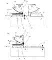
図1は本発明の剥離装置1の概略正面図、図2は剥離装置1を用いた別の実施態様を示す概略正面図、図3は剥離装置1の一要素である支持体12の別の実施態様を示す概略正面図である。また図9は、剥離装置1に用いられている剥離ユニット10の別の実施態様である剥離ユニット90の概略正面図である。
FIG. 1 is a schematic front view of a peeling device 1 of the present invention, FIG. 2 is a schematic front view showing another embodiment using the peeling device 1, and FIG. It is a schematic front view showing an embodiment. FIG. 9 is a schematic front view of a
さらに図12は本発明の剥離装置において、支持体12の可撓性フィルム支持面の回転周速度、支持体12の補強板2に対する相対移動速度および可撓性フィルムに加わる張力をモニタし上限を設定する手段の具体的な一例を説明するための剥離装置200の概略正面図、図12は剥離装置200の側面図である。
Further, FIG. 12 shows that in the peeling device of the present invention, the rotational peripheral speed of the flexible film supporting surface of the
まず、図1に記載した剥離装置1について説明する。図1に記載された剥離装置1は下記の構成を主とする。可撓性フィルム4を剥離可能な有機物層3を介してガラス基板である補強板2に接着した可撓性フィルム基板6、補強板2を保持する載置台A30と、可撓性フィルム4を補強板2から実際に剥離する剥離ユニット10、剥離した可撓性フィルム4を載置する載置台B32より構成されている。
First, the peeling device 1 shown in FIG. 1 will be described. The peeling device 1 shown in FIG. 1 mainly has the following configuration. The
載置台A30と載置台B32は、基台34にそれぞれ昇降自由に取り付けられており、図示しない駆動源により各々独立に自在に昇降できる。また、載置台A30と載置台B32の上面には各々吸引孔が配置されていて、図示していない真空源により、表面に載置されたものを各々独立に吸着保持することができる。
The mounting table A30 and the mounting table B32 are respectively attached to the
次に剥離ユニット10は、可撓性フィルム4と接する保持部14を先端に有する支持体12と、支持体12を軸16を介して片持ちで回転自在に保持するフレーム18と、フレーム18を基台34上で水平方向に自在に案内するレール20より構成される。保持部14がなく、支持体12に直接可撓性フィルムを沿わせて剥離しても良いが、クッション性を持つ保持部14や電子部品の高さを収容する凹部を設けた保持部14を採用することにより、さらに剥離によるダメージを抑制しやすくなる。軸16は図示されない回転駆動装置で駆動される。回転駆動装置の回転速度は自由に設定でき、また、軸16と回転駆動装置の間には設定以上のトルクが加わると回転駆動装置側がスリップするスリップリングが挿入されていて、可撓性フィルムに加わる張力の上限を制御できる。保持部14の表面には吸引孔が配置されている。そして図示しない真空源により、可撓性フィルム4の接触する部分を吸着することができる。保持部14に設けられた吸着孔は保持部14と可撓性フィルム4の接触した部分が順次吸引される構成になっている。また保持部14は可撓性フィルム4を湾曲して保持できるように、その可撓性フィルム4との接触面は曲面となっている。また、図示しない送風源により保持部14の表面に配置された吸着孔へ気体を送り込むことで、保持部14に保持されている可撓性フィルム4を保持部14から剥離することができる。
Next, the
保持部14の材質は特に限定されないが、プラスチックまたは、ゴム、発泡プラスチック等の弾性体であってクッション性を有することが好ましい。可撓性フィルムに傷がつくことを防止したり、後述するが電子部品に対応した凹部を形成加工しやすい、また凹部のエッジによって可撓性フィルムに折れが発生しにくいなどの効果がある。また保持部14の材質として、シリコーン樹脂等のタック性を有するものは、剥離の進行に伴い可撓性フィルムの伸びが累積して、保持部14と可撓性フィルム4との間のずれ量が増加するのを防止できることから、剥離の進行に伴う剥離角の増加を抑制でき、好ましい。タック性の目安としては保持部14から可撓性フィルム4を剥離するとき180°方向のピール強度が9.8N/m以下であることが好ましい。
The material of the
可撓性フィルムに接する支持体12または保持部14は剥離帯電による可撓性フィルムの帯電電位を抑制するために、制電性もしくは導電性であることが好ましい。帯電電位が大きくなると、放電が発生して回路パターンや電子部品を損傷するおそれがある。可撓性フィルムの剥離面とは反対の面に制電性あるいは導電性部材が接触していることによって、剥離面に発生する電荷が同じであっても電位を低くすることができるので、放電を防止できるのである。制電性材料としては、導電性材料を含有し、表面抵抗が1012Ω以下であるプラスチック、ゴム、発泡プラスチックなどが採用できる。
It is preferable that the
保持部14には、回路パターンが形成された可撓性フィルム4に許容される変形量と剥離性を勘案した曲率半径が与えられるが、部分的に異なる曲率半径が与えられていても良い。曲率半径が小さすぎると、金属からなる回路パターンが塑性変形を起こしてカールが発生したり、電子部品の端部での応力低下効果が不十分になる。一方、曲率半径が大きすぎると、可撓性フィルムの剥離に使われる力よりも可撓性フィルムを引き延ばす方向の力が大きくなりすぎて金属膜からなる回路パターンや可撓性フィルムの塑性変形の原因になる。したがって、少なくとも保持部14の可撓性フィルム4と接触する一部の曲率半径の大きさの下限値としては、好ましくは20mm以上、より好ましくは30mm以上、さらに好ましくは50mm以上である。また、少なくとも保持部14の可撓性フィルム4と接触する一部の曲率半径の大きさの上限値としては、好ましくは1000mm以下、より好ましくは800mm以下、さらに好ましくは700mm以下である。本発明において、曲率半径とは曲率を持つ部分と同じ曲率を持つ円の半径とする。
The holding
さらに、支持体12の回転とフレーム18の水平移動は、図示されていない駆動モータにより、各々独立に行われ、保持部14と可撓性フィルム4との接触部が水平方向(図中の水平矢印方向)に逐次移動するように制御される。支持体12の可撓性フィルム保持面すなわち保持部14表面での回転周速度V1を支持体の補強板に対する相対移動速度V2よりも大きくし、かつ、V1はトルク制限機構により、支持体に加わるトルクが所定の値を超えないようV2を下回らない範囲で制御する。V1、V2およびトルクの制御は、機械式、電子式もしくは、両者の組み合わせで可能である。機械式トルク制御方式としては、スリップリングと呼ばれる方式などを採用することができ、簡便な点で好ましい。電子式トルク制御方式としては、後述するようにトルクセンサーとサーボモーターの組み合わせなどで実現することができ、制御の正確さや制御の自由度が高い点で好ましい。V1、V2の初期設定値は、V1/V2が1.01以上とすることが好ましい。トルク制限の設定値は、剥離の進行に伴い剥離角が増加するのを防止するのに十分であり、かつ、金属からなる回路パターンや可撓性フィルムが塑性変形を起こさない範囲に設定されるべきであり、可撓性フィルムの材質や幅、厚さにより、適宜選択される。
Further, the rotation of the
本発明の一態様では、図7に示す剥離中の可撓性フィルム4と補強板2とのなす角である剥離角40の範囲が1°以上80°以下であることが重要である。剥離角が大きすぎると剥離点において可撓性フィルムに折れが発生することがあり、可撓性フィルム上に金属からなる回路パターンが形成されている場合は回路パターンに折れや変形が発生することがある。一方、剥離角が小さすぎると可撓性フィルムの剥離に使われる力よりも可撓性フィルムを引き延ばす方向の力が大きくなりすぎて金属膜からなる回路パターンや可撓性フィルムの塑性変形の原因になる。したがって、可撓性フィルム基板6から、可撓性フィルムを低応力で歪みなく剥離するための剥離角40の範囲は、より好ましくは2°以上70°以下、最も好ましくは5°以上60°以下である。
In one embodiment of the present invention, it is important that the range of the peeling
本発明において、剥離力は、剥離可能な有機物層を介して補強板と貼り合わせた1cm幅の可撓性フィルムを剥離するときの180°方向ピール強度で測定される。剥離力を測定するときの剥離速度は300mm/分とする。本発明において、上述の剥離角を最適な範囲内に制御するためには、剥離力が0.098N/mから98N/mの範囲であることが好ましい。 In the present invention, the peeling force is measured by a 180 ° peel strength when a 1-cm-wide flexible film bonded to a reinforcing plate via a peelable organic material layer is peeled off. The peeling speed when measuring the peeling force is 300 mm / min. In the present invention, in order to control the above-mentioned peel angle within an optimum range, the peel force is preferably in the range of 0.098 N / m to 98 N / m.
載置台A30は昇降自在であるので、可撓性フィルム4と補強板2の剥離時には、可撓性フィルム4と保持部14が一定の圧力で接触する位置まで載置台A30を昇降させて停止させる。一方、載置台B32は、剥離ユニット10の保持部14に吸着した可撓性フィルム4を載置台B32の上に載置するために設けられたものである。すなわち、剥離ユニット10は剥離完了後、可撓性フィルム4を吸着した状態で図1の破線のように、載置台B32の所まで移動する。載置台B32を昇降させて保持部14と載置台B32の間の距離を好ましくは0.1〜3mm、より好ましくは0.1〜1mmにして、吸着を解除して、可撓性フィルム4を保持部14から開放し、載置台B32に載せ替える。
Since the mounting table A30 can be moved up and down, when the
次に、図1に示す剥離装置1を用いた可撓性フィルム4の剥離方法について説明する。載置台A30を最下点まで下降させた後に、図示しない移載手段により、可撓性フィルム基板6を補強板2を下側(つまり可撓性フィルム4を上側)にして、載置台A30に載置する。続いて、図示しない真空源を稼働させて、可撓性フィルム基板6を載置台A30上に吸着保持する。次に、剥離ユニット10の保持部14の開始点Sが可撓性フィルム4の図中右端の真上に位置決めされるように、フレーム18の移動と支持体12の回転移動を行わせる。保持部14の位置決めが完了したら、載置台A30を上昇させて、可撓性フィルム4の右端と保持部14の開始点Sを所定の圧力で接触させる。圧力は好ましくは0.001〜1MPa、より好ましくは0.01〜0.2MPaである。
Next, a method of peeling the
ついでその状態で、図示しない真空源を稼働させて、保持部14を可撓性フィルム4に吸着させる。その後、フレーム18の左方向への移動と支持体12の左回転を進行させる。保持部14の曲面を(図)右側から可撓性フィルム4の上面に順次接触させる。これによって可撓性フィルム4は、右側から順次湾曲されるために、補強板2から離れていき、その結果両者の剥離が右側から順次行われることになる。保持部14の最終点Eが可撓性フィルム4の左端まできて接触し、それを通りすぎたら剥離は完了する。剥離が完了したら、フレーム18の移動と支持体12の回転を停止し、載置台A30を下降させて、可撓性フィルム4と補強板2を完全に分離した状態にする。これらの機構が本発明における引き離し手段に該当する。またこれ以外にも剥離角を80゜以下に制御することが可能であれば他の機構を用いても構わない。
Next, in this state, a vacuum source (not shown) is operated, and the holding
その後、保持部14に吸着された可撓性フィルム4の中央部が真下になるまで、支持体12を右回転させる。それからフレーム18を右方向に移動させて、保持部14に保持されている可撓性フィルム4が載置台B32の真上になるように位置決めする。つづいて、載置台B32を上昇させて、載置台B32の上面と可撓性フィルム4の中央部の最下点部のすきまが0.1〜1mmになるようにする。すきまが設定できたら、保持部14の吸着を解除して、可撓性フィルム4を載置台B32に移し替える。ついで図示しない移載装置により、分離された可撓性フィルム4と、載置台A30にある補強板2を各々次の工程に移載する。なお補強板2は吸着を解除して移載する。続いて、剥離ユニット10をもとの位置に戻して、以降同じ動作を繰り返して、次の可撓性フィルム基板6の剥離を行う。
Then, the
図2(a)に示す剥離装置は、図1の剥離装置1の支持体12の一端に、可撓性フィルム4の端部をかぎ型に保持する保持部材22を固定したものである。保持部材22の材質は特に限定されず、例えば、金属、樹脂、セラミックス等を使用することができるが、本体を金属にして可撓性フィルム4との接触部をゴムや樹脂等の柔らかく、かつ、滑りにくいものにした複合構造等が好ましく使用される。
The peeling device shown in FIG. 2A has a structure in which a holding
図2(a)に示す剥離装置を使用した剥離方法は次の通りである。 The peeling method using the peeling device shown in FIG. 2A is as follows.
載置台A30を最下点まで下降させ、ついで保持部14が載置台A30の真上にこないようにフレーム18を右側に移動させる。この状態で図示しない移載手段により、可撓性フィルム基板6を補強板2を下側(可撓性フィルム4を上側)にして、載置台A30に載置する。続いて、図示しない真空源を稼働させて、可撓性フィルム基板6を載置台A30上に吸着保持する。
The mounting table A30 is lowered to the lowest point, and then the
次に、保持部材22のかぎ型になっている部分が、可撓性フィルム4の右端部にはまる位置にくるよう、載置台A30を上昇させる。そして、フレーム18を左側に移動させて、図2(a)に示すように、保持部材22のかぎ型部に可撓性フィルム4の右端部をはまりこませて、保持部材22で可撓性フィルム4の右端部が保持できるようにする。この時の保持部材22のかぎ型部と可撓性フィルム4右端部の厚さ方向のすきまは、好ましくは0.1〜5mm、より好ましくは0.5〜1.5mmである。
Next, the mounting table A30 is raised so that the hook-shaped portion of the holding
可撓性フィルム4の端部を保持部材22で保持するためには補強板2から可撓性フィルム4の端部がはみ出していてもよい。また、図2(b)に示すように、別の方法で可撓性フィルム4の端部にリードフィルム23を貼り合わせた可撓性フィルム基板6を載置台A30に載置し、リードフィルム23の端部を保持部材22で保持してもよい。
In order to hold the end of the
ついでその状態で、フレーム18の左方向への移動と支持体12の左回転を同期して行って、保持部14の曲面を(図)右側から可撓性フィルム4の上面に順次接触させる。これによって可撓性フィルム4が湾曲しながらその右端部が順次上に持ち上げられ、吸着保持されている補強板2から引き離されることになるので、両者の剥離が右側から順次行われる。保持部14の最終点Eが可撓性フィルム4の左端まできて接触し、それを通りすぎたら剥離は完了する。剥離が完了したら、フレーム18の移動と支持体12の回転を停止し、載置台A30を下降させて、可撓性フィルム4と補強板2を完全に分離した状態にする。
Then, in this state, the leftward movement of the
その後、フレーム18を右方向へ移動させて、保持部材22で保持されていない側の可撓性フィルムの端部が載置台B32の端部と合うように位置決めする。その状態で、フレーム18の右方向への移動と支持体12の右回転を同期して行って可撓性フィルム4を載置台B32へ移し替えて行く。
After that, the
ついで、保持部材22の保持を解除して、フレーム18をさらに右側に移動させて、保持部材22のかぎ型部分から可撓性フィルム4の右端部が外れるようにし、可撓性フィルム4を載置台B32に完全に移し替える。移し替えが完了したら、載置台B32を最下点まで下降させる。ついで図示しない移載装置により、分離された可撓性フィルム4と補強板2を各々次の工程に移載する。続いて、剥離ユニット10をもとの位置に戻して、以降同じ動作を繰り返して、次の可撓性フィルム基板6の剥離を行う。
Subsequently, the holding of the holding
なお、可撓性フィルム4上にICチップ等の電子部品5が搭載されている場合は、支持体12の保持部14には、図3に示すように、電子部品5に対応した凹部36が設けられることが好ましい。凹部36のサイズ変更は、アダプターを設けることで行ってもよい。ICチップに対応する凹部のサイズの例としては、図4に示すように深さ0.5〜2mm、縦横1〜20mmである。また、凹部の形状はICチップが複数個納まるような溝状であってもよく、溝の方向は、図5に示すように保持部14の曲率方向と平行であってもよいし、図6に示すように保持部14の曲率方向と直行していてもよい。さらに、凹部36の底面74にも吸引孔を設け、かつ底面74と電子部品が接触して、電子部品5も保持部14に吸着固定できるようにしてもよい。さらに、保持部14を真空吸着できるマイクロポアを持つ柔軟な素材で作製し、電子部品5を該素材中に埋め込んで吸着固定することも可能である。
When the
本発明は、可撓性フィルム4上に金属からなる回路パターンが設けられている場合、剥離するときの力で回路パターンが変形し、可撓性フィルム4に反りが発生したり、回路パターン寸法精度が低下することを防止し、さらに、ICチップ等の電子部品が可撓性フィルムからなる回路基板に搭載されると、電子部品搭載部分を剥離するための力が大きくなるとともに電子部品端部に力が集中し、回路基板が変形する場合があるので、本発明を実施することで変形、反り、寸法精度等に対する信頼性を奏することができる。またICチップなどの電子部品に樹脂封止が施されている場合でも剥離時に電子部品の端部に加わる応力が緩和され、回路基板の信頼性が向上するので好ましい。
According to the present invention, when a circuit pattern made of metal is provided on the
載置台A30による可撓性フィルム基板6の保持方法は特に限定されず、上記の実施態様で示した真空吸着の他、静電気吸着であってもよい。静電気吸着が行えるようにするには、載置台A30は導電性でかつ、静電気の付与の方法に応じて接地電位や任意の電圧が印加できる構造にすることが望ましい。また、載置台A30には、剥離可能な有機物層3の剥離力を低下させるために、内部または上部に加熱装置が付与されていることが好ましい。同じ目的で、支持体12または保持部14に加熱装置が付与されていることが好ましい。十分に剥離力を低減するためには加熱温度は高温の方が好ましいが、加熱温度が高すぎると有機物層が変質して剥離後の可撓性フィルム4上に残存する有機物層を除去しにくくなるため、剥離可能な有機物層3の加熱温度は、30℃以上280℃以下であることが好ましい。
The method of holding the
次に本発明の実施態様例である剥離装置200を、図11、12を用いて説明する。剥離装置200では、剥離装置1の剥離ユニット10に、スリップリングに変えて、支持体12の可撓性フィルム支持面の回転周速度、支持体12の補強板2に対する相対移動速度および可撓性フィルムに加わる張力をモニタし上限を設定するための電気的制御手段が付加されて剥離ユニット220に変更されている。より具体的に記載すると、剥離装置200は、フレーム18の載置台A30(固定)に対する相対移動速度V2を測定するリニアスケール202、支持体12の回転角速度を測定するエンコーダ204と支持体12に与えるトルクを制御する電磁クラッチ206とを剥離装置1に追加したものである。軸16の中心から、保持部14がその保持面で可撓フィルム基板6の可撓性フィルム4に接触するまでの長さをRとすると、このRにエンコーダ204で観測された回転角速度を掛け合わせることにより、保持部14保持面での回転周速度V1が算出される。なお保持部14保持面は、支持体12の可撓性フィルム支持面と同義である。さらに剥離装置200には、上記のエンコーダ204での測定から導出される保持部14保持面での回転周速度V1や、リニアスケール202によって測定されるフレーム18の相対移動速度V2の速度情報により、支持体12を電磁クラッチ206と軸16を介して回転駆動する回転モータ210と、フレーム18を駆動するリニアモータ208とを速度制御することができる制御装置212も、剥離装置1に対して追加されている。ここで制御装置212は、電磁クラッチ206への供給電圧を変えることで、支持体12の駆動トルクを制御する機能も有している。なお、回転モータ210と電磁クラッチ206は支持ブラケット214を介してフレーム18に取り付けられている。
Next, a
また、フレーム18が相対移動速度V2で移動するときは、それに取り付けられている支持体12も同じく相対移動速度V2で移動する。
Further, when the
さて剥離装置200では、可撓フィルム基板6の可撓性フィルム4を補強板2から剥離する時に、図7で示されている剥離角40を、制御することができる。
すなわち保持部14保持面での回転周速度V1をフレーム18の相対移動速度V2よりも小さくすると、可撓性フィルム4はたるんでくるとともに、図7の剥離点Pも位置が変動し、剥離が非常に不安定となる。この時、V1/V2の大きさが小さくなるほど、剥離点Pが右側に移動するので、不安定な挙動を示しながらも、剥離角40の大きさは大きくなる。一方、保持部14保持面での回転周速度V1をフレーム18の相対移動速度V2よりも大きくすると、可撓性フィルム4に支持体12より張力が付加される。このV1/V2>1の状態では、V1/V2の大きさが大きくなると可撓性フィルム4に作用する張力が大きくなり、さらに剥離点Pが図7で左側に移動するので、剥離角40は次第に小さくなる。また可撓性フィルム4のたるみがないので剥離点Pの位置も安定化し、その結果剥離が安定化する。したがって、剥離が安定化するV1/V2>1の条件で、V1/V2の大きさを調整することで、剥離角40を所望の値にすることができる。
Now, in the
That is, when the rotational peripheral speed V1 on the holding surface of the holding
ただし、V1/V2が大きくなりすぎると、可撓性フィルム4に加わる張力も大きくなりすぎて、可撓性フィルム4が大きく変形し、可撓性フィルム4上に形成される精密な回路パターンの寸法形状が変化したり、回路パターンが破損して不良となる場合がある。
However, if V1 / V2 is too large, the tension applied to the
このような不都合を解消するために、剥離時に可撓性フィルム4に作用する張力を問題の生じない大きさ以下に制限することが好ましい。剥離装置200では、電磁クラッチ206への供給電圧を調整して、支持体12に加わるトルクが所定の値以下になるようにトルク制御できる。支持体12の保持部14では可撓性フィルム4が保持されるから、支持体12に加わるトルクは可撓性フィルムに作用する張力に変換される。したがって、支持体12に加わるトルクを制限すれば、可撓性フィルム4に作用する張力を制限することができる。ただこの場合、トルクが制限値に達していると、支持体12の軸16の回転が回転モータ210の回転に対して滑る状態にあり、回転モータ210は保持部14保持面での回転周速度V1が所定の値になるよう動作していても、実際の保持部14保持面での回転周速度V1は、電磁クラッチ206で滑らない状態の時よりも小さくなる。そして実際の保持部14保持面での回転周速度V1の大きさは、トルク制限値に依存して定まることになる。この時にもV1/V2>1、さらには所望の範囲の剥離角40を得られるよう、トルクの制限値を選定することが望ましい。
In order to eliminate such inconveniences, it is preferable to limit the tension acting on the
以上剥離装置200は、保持部14保持面での回転周速度V1と相対移動速度V2を調整し、V1/V2>1として剥離を安定化させる一方、支持体12に加わるトルクを調整することで可撓性フィルム4に作用する張力を制限できるので、可撓性フィルム4を変形させることなく、さらには可撓性フィルム4上の回路パターンを損なうことなく、安定して剥離を行わせることができる。
As described above, the
剥離装置200では、V1/V2>1とし、さらに可撓性フィルムへの作用張力を制限する制御を、制御装置212により、上記の電磁クラッチ206を用いたトルク制御で行うことの他、保持部14保持面での回転周速度V1とフレーム18の相対移動速度V2の速度制御で行うこともできる。ここでいう速度制御とは、まず電磁クラッチ206への供給電圧を大きくして制限トルクを大きくすることで支持体12の回転が回転モータ210の回転に対して滑らない状態にし、さらにV1/V2が1より大きい適切な値になるように、回転モータ210の回転速度とリニアモータ208によるフレーム18の相対移動速度V2を制御するものである。V1/V2が大きくなれば可撓性フィルム4への作用張力は大きくなるので、制限される張力の大きさになるようV1/V2を定める。
In the
以上の速度制御、トルク制御のいずれを用いてもよいが、トルク制御の場合は、長時間の剥離の進行で可撓性フィルム4の伸びが累積してたるみが生じ、剥離角40が増加するのを防止でき、常に回路パターンが形成された可撓性フィルムを低応力で剥離できる。
Any of the above speed control and torque control may be used, but in the case of torque control, the elongation of the
なお、電磁クラッチ206を用いたトルク制御は、スリップリング等の他の機械式トルク制御方式でもよいし、トルクセンサーとサーボモーターの組み合わせ等で実現する電子式トルク制御方式であってもよい。また機械式と電子式トルク制御方式の両者の組み合わせも可能である。保持部14の保持面での回転周速度V1とフレーム18の相対移動速度V2の比率V1/V2は1.01以上とすることが好ましい。支持体12へのトルクや可撓性フィルム4に作用する張力の制限値は、剥離の進行に伴い剥離角が増加するのを防止するのに十分であり、かつ、金属からなる回路パターンや可撓性フィルムが塑性変形を起こさない範囲に設定することが必要で、可撓性フィルムの材質や幅、厚さにより、適宜選択される。可撓性フィルム4に作用させる張力としては、好ましくは300N/m以下、より好ましくは200N/m以下である。
The torque control using the
剥離装置200を用いた可撓性フィルム4の剥離方法は、制御装置212により、1)剥離角40が所望の値になるようV1/V2>1を満たす適切な値を選定する、2)回転モータ210を所定の保持部14保持面での回転周速度V1になるよう速度制御する、3)リニアモータ208を駆動してフレーム18の相対移動速度V2を所定の値になるよう速度制御する、4)電磁クラッチ206への供給電圧を調整して、支持体12に加わるトルクを制限して、剥離時の可撓性フィルム4への張力を制限することの他、剥離装置1による可撓性フィルム4の剥離方法と全く同じである。
The method of peeling the
なお剥離装置1で、剥離ユニット10は、図8に示す剥離ユニット80や、図9に示す剥離ユニット90に置き換えることも可能である。剥離ユニット80は、可撓性フィルム4を剥離可能な有機物層3を介してガラス基板である補強板2に接着した可撓性フィルム基板6の補強板2を保持する載置台A30と、可撓性フィルム4を保持し、矢印で示した剥離角40の延長線方向へ引っ張ることにより剥離可能な有機物層3から可撓性フィルム4を剥離する引き剥がし部材81より構成されている。
In the peeling apparatus 1, the peeling
引き剥がし部材81は図示しない駆動源により可撓性フィルム4の端部を保持し、剥離角40を1°以上80°以下の範囲に保ちつつ可撓性フィルム4を引っ張ることができるが、剥離角40をより安定して制御するには、以下説明する剥離ユニット90を用いるのが好ましい。
The peeling
図9にある剥離ユニット90は、可撓性フィルム4を剥離可能な有機物層3を介してガラス基板である補強板2に接着した可撓性フィルム基板6の補強板2を保持する載置台92と、可撓性フィルム4の端部を保持し、矢印で示した剥離角40の延長線方向へ引っ張ることにより剥離可能な有機物層3から可撓性フィルム4を剥離する引き剥がし部材91、剥離の際に可撓性フィルム4を支持するために、フレーム94に取り付けられた支持ロール95より構成される。
A peeling
載置台92とフレーム94は剥離装置1の基台34に取り付けられており、図示しない駆動源とガイドにより各自独立に水平方向へ移動することができる。支持ロール95は図示しない駆動源により回転させることも、駆動源から切り離すことで自由ロールとすることも、回転しないように固定することもできる。
The mounting table 92 and the
引き剥がし部材91は図示しない駆動源により可撓性フィルム4の端部を保持し、載置台92を移動させるのと連動して、可撓性フィルム4を矢印で示した剥離角40の延長線方向へ引っ張ることにより、剥離角40を1°以上80°以下の範囲に保ちつつ剥離することができる。剥離が行われる時に支持ロール95が取り付けられているフレーム94は停止していてもよいし、矢印の方向、すなわち載置台92の移動方向とは逆方向に移動してもよい。
The peeling
また、別の実施態様として、引き剥がし部材91を図示しない駆動源により可撓性フィルム4の端部を保持し、フレーム94を矢印の方向、すなわち図9の左方向に移動させるのと連動して、可撓性フィルム4を引っ張ることにより、剥離角40を1°以上80°以下の範囲に保ちつつ剥離することもできる。剥離が行われるときに、載置台92は停止していてもよいし、フレーム94とは逆方向に移動していてもよい。
In another embodiment, the peeling
剥離ユニット90を用いて剥離を行う時は、可撓性フィルム4は必ず支持ロール95の表面に支持されていることが好ましい。それによって可撓性フィルムが支持ロールによって案内されることになるので、剥離が安定して行われる。また剥離を行う時に支持ロール95は、可撓性フィルム4との接触面での周速度が可撓性フィルムの移動速度と略同一になるように駆動するか、回転フリーであることが好ましい。これによって支持ロール95と可撓性フィルム4の間にすべりがなくなり、可撓性フィルム4に傷をつける等の不具合を防止することができる。剥離を行う時に支持ロール95は回転固定であってもよいが、可撓性フィルム4表面へのダメージが無視されうる時に用いられることが好ましい。
When peeling is performed using the
なお剥離ユニット80、90は剥離装置200の剥離ユニット220に置きかえて使用してもよい。
The peeling
本発明に使用する補強板2としては、ソーダライムガラス、ホウケイ酸系ガラス、石英ガラスなどの無機ガラス類からなる板、アルミナ、窒化シリコン、ジルコニアなどのセラミックス、ステンレススチール、インバー合金、チタンなどの金属やガラス繊維補強樹脂からなる板など、線膨張係数や吸湿膨張係数が小さいものが好ましい。その中でも、適当な可撓性が得られやすい点で、無機ガラスと金属からなる板が好ましい。さらに、耐熱性、耐薬品性に優れている点、大面積で表面平滑性が高く基板が安価に入手しやすい点、塑性変形しにくい点、搬送装置などとの接触によりパーティクルを発生しにくい点、絶縁体で電解めっきによる析出がない点、等により、無機ガラス類からなる板が特に好ましい。
Examples of the reinforcing
補強板に厚みが小さいガラス基板を用いる場合、可撓性フィルムの膨張・収縮力で反りやねじれが大きくなり、平坦な載置台上に真空吸着したときにガラス基板が割れることがある。また、真空吸着・脱着で可撓性フィルムが変形することになり、位置精度の確保が難しくなる傾向がある。一方、厚みが大きいガラス基板では、剥離のために湾曲しにくくなる上に、肉厚ムラにより平坦性が低下したり、露光精度も低くなる。また、ロボット等によるハンドリング負荷が大きくなり素早い動作ができずに生産性が低下する要因になる他、運搬コストも増大する。これらの点から、ガラス基板の厚さは、0.3mmから1.1mmの範囲が好ましい。 When a glass substrate having a small thickness is used for the reinforcing plate, warping and torsion increase due to expansion and contraction forces of the flexible film, and the glass substrate may be broken when vacuum-adsorbed on a flat mounting table. In addition, the flexible film is deformed by vacuum suction / detachment, which tends to make it difficult to secure positional accuracy. On the other hand, in the case of a glass substrate having a large thickness, the glass substrate is not easily curved due to peeling, and the thickness unevenness lowers flatness and lowers the exposure accuracy. In addition, the handling load of a robot or the like increases, and quick operation cannot be performed, which causes a decrease in productivity and increases transportation costs. From these points, the thickness of the glass substrate is preferably in the range of 0.3 mm to 1.1 mm.
補強板に厚みが小さい金属基板を用いる場合、可撓性フィルムの膨張・収縮力で反りやねじれが大きくなり、平坦な載置台上に真空吸着できなくなったり、金属基板の反りやねじれが発生する分だけ可撓性フィルムが変形することにより、所定の位置精度が確保できなくなる。また、折れがあるとその時点で不良品になる。一方、厚みが大きい金属基板では、肉厚ムラにより平坦性が低くなるとともに、剥離のための湾曲が行いにくくなり、露光精度も低下する。また、ロボット等によるハンドリング負荷が大きくなり、素早い動作ができなくなって生産性が低下する他、運搬コストも増大する。したがって、金属基板の厚さは、0.1mmから0.7mmの範囲が好ましい。 When a metal substrate with a small thickness is used for the reinforcing plate, the warpage and torsion increase due to the expansion and contraction force of the flexible film, and the vacuum suction cannot be performed on a flat mounting table, or the warpage and torsion of the metal substrate occur. When the flexible film is deformed by a certain amount, the predetermined positional accuracy cannot be secured. Also, if there is a break, it becomes defective at that time. On the other hand, in the case of a metal substrate having a large thickness, flatness is reduced due to thickness unevenness, and bending for peeling becomes difficult, and exposure accuracy is also reduced. In addition, the handling load of the robot or the like increases, and quick operation cannot be performed. As a result, productivity decreases, and transport costs increase. Therefore, the thickness of the metal substrate is preferably in the range of 0.1 mm to 0.7 mm.
本発明において、可撓性フィルムとしては、プラスチックフィルムを使用する。例えば、ポリカーボネート、ポリエーテルサルファイド、ポリエチレンテレフタレート、ポリエチレンナフタレート、ポリフェニレンサルファイド、ポリイミド、ポリアミド、液晶ポリマーなどのフィルムを採用することができる。中でもポリイミドフィルムは、耐熱性に優れるとともに耐薬品性にも優れているので好適に採用される。また、低誘電損失など電気的特性が優れている点や低吸湿性の点で、液晶ポリマーが好適に採用される。可撓性のガラス繊維補強樹脂板を採用することも可能である。また、これらのフィルムが積層されていてもよい。 In the present invention, a plastic film is used as the flexible film. For example, films such as polycarbonate, polyether sulfide, polyethylene terephthalate, polyethylene naphthalate, polyphenylene sulfide, polyimide, polyamide, and liquid crystal polymer can be employed. Among them, a polyimide film is preferably used because it has excellent heat resistance and chemical resistance. In addition, a liquid crystal polymer is preferably used in terms of excellent electrical characteristics such as low dielectric loss and low hygroscopicity. It is also possible to employ a flexible glass fiber reinforced resin plate. Further, these films may be laminated.
上記ガラス繊維補強樹脂板の樹脂としては、例えば、エポキシ、ポリフェニレンサルファイド、ポリフェニレンエーテル、マレイミド(共)重合樹脂、ポリアミド、ポリイミドなどが挙げられる。 Examples of the resin of the glass fiber reinforced resin plate include epoxy, polyphenylene sulfide, polyphenylene ether, a maleimide (co) polymer resin, polyamide, and polyimide.
可撓性フィルムの厚さは、軽量化、小型化、あるいは微細なビアホール形成のためには薄い方が好ましく、一方、機械的強度を確保するためや平坦性を維持するためには厚い方が好ましい点から、4μmから125μmの範囲が好ましい。 The thickness of the flexible film is preferably thin for weight reduction, miniaturization, or formation of fine via holes, while thicker for securing mechanical strength and maintaining flatness. From a preferable point, the range of 4 μm to 125 μm is preferable.
本発明に用いられる剥離可能な有機物層としては、接着剤または粘着剤が使用される。剥離可能な接着剤または粘着剤としては、例えば、アクリル系またはウレタン系の再剥離剤と呼ばれる粘着剤を挙げることができる。可撓性フィルム加工中は十分な接着力があり、剥離時は容易に剥離でき、可撓性フィルム基板に歪みを生じさせないために、弱粘着から中粘着と呼ばれる領域の粘着力のものが好ましい。タック性があるシリコーン樹脂を使用することもできる。また、タック性があるエポキシ系樹脂を使用することも可能である。 As the peelable organic material layer used in the present invention, an adhesive or a pressure-sensitive adhesive is used. Examples of the peelable adhesive or pressure-sensitive adhesive include pressure-sensitive adhesives called acrylic or urethane-based re-release agents. In order to have sufficient adhesive strength during the processing of the flexible film, to be easily peelable at the time of peeling, and not to cause distortion in the flexible film substrate, those having an adhesive strength in an area called weak adhesive to medium adhesive are preferable. . A tacky silicone resin can also be used. It is also possible to use an epoxy resin having tackiness.
剥離可能な有機物としては、低温領域で接着力、粘着力が減少するもの、紫外線照射で接着力、粘着力が減少するものや加熱処理で接着力、粘着力が減少するものも好適に用いられる。これらの中でも紫外線照射によるものは、接着力、粘着力の変化が大きく好ましい。紫外線照射で接着力、粘着力が減少するものの例としては、2液架橋型のアクリル系粘着剤が挙げられる。また、低温領域で接着力、粘着力が減少するものの例としては、結晶状態と非結晶状態間を可逆的に変化するアクリル系粘着剤が挙げられ、好ましく使用される。 As the releasable organic substance, those whose adhesive strength and adhesive strength are reduced in a low temperature region, those whose adhesive strength and adhesive strength are reduced by ultraviolet irradiation, and those whose adhesive strength and adhesive strength are reduced by heat treatment are also preferably used. . Among them, those obtained by irradiation with ultraviolet rays are preferable because the change in adhesive strength and adhesive strength is large. As an example of the adhesive force and the adhesive force that are reduced by the irradiation of ultraviolet rays, a two-component cross-linkable acrylic pressure-sensitive adhesive can be used. Further, as an example of an adhesive whose adhesive strength and adhesive strength decrease in a low temperature region, an acrylic adhesive which reversibly changes between a crystalline state and an amorphous state can be mentioned, and is preferably used.
本発明に使用する剥離可能な有機物層の厚みは、薄すぎると平面性が悪くなる他、剥離力が大きく低下するために膜厚のむらによる剥離力の強度むらが発生するため、0.1μm以上であることが好ましく、0.3μm以上であることがさらに好ましい。一方、剥離可能な有機物層の厚みが厚すぎると有機物層の可撓性フィルムへの投錨性がよくなるために粘着力が強くなりすぎるため、10μm以下であることが好ましく、20μm以下であることがさらに好ましい。補強板上に剥離可能な有機物層を介して固定された可撓性フィルム上の回路パターンに電子部品を接合する場合は、回路パターンの厚み方向の変化を抑制するため剥離可能な有機物層の厚みが5μm以下であることが好ましい。剥離可能な有機物層が厚いと電子部品を加熱圧接する際に、剥離可能な有機物層の変形量が大きく、接合部の回路パターンが沈み込み、配線回路の信頼性に問題が生じることがある。沈み込みが大きいときには、電子部品のエッジに回路パターンが接触して短絡を生じることがある。該沈み込みは、配線回路の信頼性を確保するために6μm以下であることが好ましく、3μm以下であることがさらに好ましい。 The thickness of the releasable organic layer used in the present invention is not more than 0.1 μm because, when the thickness is too small, the flatness is deteriorated, and the strength of the peeling force due to the unevenness of the film thickness occurs because the peeling force is significantly reduced. Is more preferable, and more preferably 0.3 μm or more. On the other hand, if the thickness of the peelable organic material layer is too thick, the anchoring property of the organic material layer to the flexible film is improved, so that the adhesive strength becomes too strong, so that the thickness is preferably 10 μm or less, and preferably 20 μm or less. More preferred. When joining an electronic component to a circuit pattern on a flexible film fixed via a peelable organic material layer on a reinforcing plate, the thickness of the peelable organic material layer is controlled to suppress a change in the thickness direction of the circuit pattern. Is preferably 5 μm or less. When the peelable organic material layer is thick, when the electronic component is heated and pressed, the amount of deformation of the peelable organic material layer is large, and the circuit pattern of the bonding portion sinks, which may cause a problem in the reliability of the wiring circuit. When the sink is large, the circuit pattern may come into contact with the edge of the electronic component to cause a short circuit. The sink is preferably 6 μm or less, more preferably 3 μm or less, to ensure the reliability of the wiring circuit.
可撓性フィルムと補強板とを剥離することを考慮すると、剥離可能な有機物層と補強板との粘着力の方が、剥離可能な有機物層と可撓性フィルムとの粘着力よりも大きいことが好ましい。このように両側の粘着力を制御する方法として、例えば、粘着剤の熟成を利用する方法がある。すなわち、粘着力を強くする側に粘着剤を塗布してから、空気を遮断した状態で所定の期間架橋を進行させることで、粘着力が低下した表面を得ることができる。 Considering the peeling of the flexible film and the reinforcing plate, the adhesive strength between the peelable organic layer and the reinforcing plate is larger than the adhesive strength between the peelable organic layer and the flexible film. Is preferred. As a method of controlling the adhesive strength on both sides in this way, for example, there is a method of utilizing aging of the adhesive. That is, by applying a pressure-sensitive adhesive on the side where the pressure-sensitive adhesive strength is increased, and then proceeding with crosslinking for a predetermined period in a state where air is shut off, a surface having a reduced pressure-sensitive adhesive force can be obtained.
本発明の回路基板の製造方法における可撓性フィルム基板6の製造例を以下に説明するが、本発明は、これに限定されるものではない。
An example of manufacturing the
厚さ1.1mmのアルミノホウケイ酸塩ガラスに、スピンコーター、ブレードコーター、ロールコーター、バーコーター、ダイコーター、スクリーン印刷などを用いて、剥離可能な有機物を塗布する。間欠的に送られてくる枚葉基板に均一に塗布するためには、ダイコーターの使用が好ましい。剥離可能な有機物塗布後、加熱乾燥や真空乾燥などにより乾燥し、厚みが2μmの剥離可能な有機物層を得る。塗布した剥離可能な有機物層上に、離型フィルム(ポリエステルフィルム上にシリコーン樹脂層を設けた)からなる空気遮断用フィルムを貼り合わせて1週間室温で放置する。この期間は、熟成と呼ばれ、剥離可能な有機物の架橋が進行して、徐々に粘着力が低下する。放置期間や保管温度は、所望の粘着力が得られるように選択される。空気遮断用フィルムを貼り合わせる代わりに、窒素雰囲気中や真空中で保管することもできる。剥離可能な有機物を長尺フィルム基体に塗布、乾燥後、補強板に転写することも可能である。 A releasable organic material is applied to a 1.1 mm-thick aluminoborosilicate glass using a spin coater, a blade coater, a roll coater, a bar coater, a die coater, screen printing, or the like. The use of a die coater is preferred in order to uniformly apply the liquid to the intermittently fed single-wafer substrate. After the peelable organic material is applied, the film is dried by heating drying or vacuum drying to obtain a peelable organic material layer having a thickness of 2 μm. An air-blocking film made of a release film (a silicone resin layer is provided on a polyester film) is attached to the applied peelable organic material layer, and left at room temperature for one week. This period is called aging, and the crosslinking of the peelable organic substance progresses, and the adhesive strength gradually decreases. The leaving period and the storage temperature are selected so as to obtain a desired adhesive strength. Instead of laminating the air blocking film, it can be stored in a nitrogen atmosphere or in a vacuum. It is also possible to apply a peelable organic substance to a long film substrate, dry it, and then transfer it to a reinforcing plate.
次に、厚さ25μmのポリイミドフィルムを準備する。ガラス基板上の空気遮断用フィルムを剥がして、ポリイミドフィルムをガラス基板に貼り合わせる。前述のように、ポリイミドフィルムの片面または両面に金属層(回路パターンであってもよい)があらかじめ形成されていても良い。ポリイミドフィルムはあらかじめ所定の大きさのカットシートにしておいて貼り付けても良いし、長尺ロールから巻きだしながら、貼り付けと切断をしてもよい。このような貼り付け作業には、国際公開第03/009657号パンフレットで提案された可撓面状体の面にポリイミドフィルムを保持してから、ガラス基板に押圧することで、低応力、高精度にポリイミドフィルムをガラス基板側にラミネートする方法が好適に採用できる。このようなラミネート装置について図10を用いて説明する。10はラミネート装置の概略正面図である。静電気耐電装置104で可撓性面状体102を帯電させ、ポリイミドフィルム4を吸着させる。可撓性面状体102には可撓性の織物や薄膜状物が採用でき、枠体113に固定されている。また、静電気帯電装置104は基台105上の支柱115に支持されており、図示されていない上下動機構によって、支柱115は、図10の左右に移動する枠体113や載置台101と静電気帯電装置104が干渉しないように動く。次に、剥離可能な有機物層2が塗布されたガラス基板2を真空吸着等で載置台101に保持する。スキージ103でポリイミドフィルム4を可撓性面状体102ごと剥離可能な有機物層3に押しつけ、ポリイミドフィルム4をガラス基板2側に移し取る。スキージ103はスキージ保持体114に保持されており、移動や上下動が可能である。載置台101は、レール106、ガイド107、ナット108、ボールねじ111、モーター112によって図の左右に移動できる。
Next, a polyimide film having a thickness of 25 μm is prepared. The film for air blocking on the glass substrate is peeled off, and the polyimide film is bonded to the glass substrate. As described above, a metal layer (which may be a circuit pattern) may be previously formed on one or both sides of the polyimide film. The polyimide film may be pasted in a cut sheet of a predetermined size, or may be pasted and cut while being wound from a long roll. For such a sticking operation, a polyimide film is held on the surface of a flexible flat body proposed in the pamphlet of WO 03/009657, and then pressed against a glass substrate to obtain low stress, high precision. And a method of laminating a polyimide film on the glass substrate side. Such a laminating apparatus will be described with reference to FIG. 10 is a schematic front view of the laminating apparatus. The flexible
ポリイミドフィルムの貼り合わせ面とは反対側の面に金属層(回路パターンであってもよい)が設けられていない場合は、フルアディティブ法やセミアディティブ法で金属層を形成する。さらに必要に応じて金、ニッケル、錫などのめっきを施して、回路パターンを得る。 When a metal layer (may be a circuit pattern) is not provided on the surface opposite to the bonding surface of the polyimide film, the metal layer is formed by a full additive method or a semi-additive method. Further, if necessary, plating of gold, nickel, tin or the like is performed to obtain a circuit pattern.
また、回路パターン形成において、ポリイミドフィルムに接続孔を設けることができる。すなわち、枚葉基板との貼り合わせ面側に設けた金属層との電気的接続を取るビアホールを設けたり、ボールグリッドアレイのボール設置用の孔を設けたりすることができる。接続孔の設け方としては、レーザー孔開けやケミカルエッチングを採用することができる。電気的接続を取る場合は、接続孔形成後、前述の回路パターン形成と同時にめっき法で孔内面を導体化することが好ましい。電気的接続をとるための接続孔は、直径が15μmから200μmが好ましい。ボール設置用の孔は、直径が50μmから800μmが好ましく、80μmから800μmがより好ましい。 In forming a circuit pattern, a connection hole can be provided in the polyimide film. That is, it is possible to provide a via hole for making an electrical connection with a metal layer provided on the surface to be bonded to the single-wafer substrate, or to provide a hole for placing a ball of a ball grid array. Laser holes or chemical etching can be used as the method of providing the connection holes. In the case of making an electrical connection, it is preferable that after forming the connection hole, the inner surface of the hole is made conductive by plating simultaneously with the formation of the circuit pattern. The diameter of the connection hole for making electrical connection is preferably 15 μm to 200 μm. The diameter of the hole for ball installation is preferably 50 μm to 800 μm, more preferably 80 μm to 800 μm.
必要に応じて、回路パターン上にソルダーレジスト層を形成する。ソルダーレジストとしては、感光性のソルダーレジストや熱硬化性のソルダーレジストが好ましい。その中でも、微細回路パターンに対しては感光性のソルダーレジストの採用がより好ましい。スピンコーター、ブレードコーター、ロールコーター、バーコーター、ダイコーター、スクリーン印刷機などで回路パターン上に感光性ソルダーレジストを塗布し、乾燥させた後、所定のフォトマスクを介して紫外線露光をし、現像して、ソルダーレジストパターンを得る。次に100℃から200℃でキュアをする。 If necessary, a solder resist layer is formed on the circuit pattern. As the solder resist, a photosensitive solder resist or a thermosetting solder resist is preferable. Among them, it is more preferable to use a photosensitive solder resist for a fine circuit pattern. Apply a photosensitive solder resist on the circuit pattern with a spin coater, blade coater, roll coater, bar coater, die coater, screen printer, etc., dry it, expose it to ultraviolet light through a predetermined photomask, and develop Thus, a solder resist pattern is obtained. Next, curing is performed at 100 ° C. to 200 ° C.
次いで形成した回路パターン上にICチップ、抵抗やコンデンサなどの電子部品を実装する。電子部品を搭載させる手段は、光学的位置検出機能と可動ステージなどの位置合わせ機能を有し、搭載精度を確保できる装置を用いて行うことが好ましい。 Next, electronic components such as an IC chip, a resistor and a capacitor are mounted on the formed circuit pattern. The means for mounting the electronic component is preferably performed by using a device that has an optical position detection function and a positioning function such as a movable stage and can ensure mounting accuracy.
また、電子部品と回路基板との接続方法としては、回路基板の接続部に形成された錫、金、はんだなどの金属層と電子部品の接続部に形成された金やはんだなどの金属層とを加熱圧着し金属接合させる方法、回路基板の接続部の錫、金、はんだなどの金属層と電子部品の接続部に形成された金やはんだなどの金属層とを圧着しつつ回路基板と電子部品間に配置した異方導電性接着剤または非導電性接着剤を硬化させ、機械的に接合させる方法などが挙げられる。 In addition, as a method for connecting the electronic component to the circuit board, a metal layer such as tin, gold, or solder formed at the connection portion of the circuit board and a metal layer such as gold or solder formed at the connection portion of the electronic component may be used. A metal layer such as tin, gold, or solder at the connection part of the circuit board and a metal layer such as gold or solder formed at the connection part of the electronic component by pressing and bonding the circuit board to the metal. A method of curing an anisotropic conductive adhesive or a non-conductive adhesive disposed between components and mechanically joining them is exemplified.
回路パターンの保護や可撓性フィルムを歪みなく剥離するために、可撓性フィルム基板6上の全面あるいは一部に保護層を形成することが好ましい。すなわち、保護層を形成することによって、可撓性フィルム剥離の際の剥離角が大きくなり過ぎることを抑制する効果が得られるからである。可撓性フィルム上に保護層を設けて、可撓性フィルムを剥離した後、保護層を除去することでも同様の効果を得ることができる。保護層の形成はフィルム状の部材をラミネートしてもよいし、液状材料をコーティングしてもよい。保護層が液状の場合、スピンコーター、ブレードコーター、ロールコーター、バーコーター、ダイコーター、スクリーン印刷機、カーテンコーターなどで可撓性フィルム基板上に溶液を塗布し、乾燥させる。さらに保護層は補強板から回路基板を剥離した後に水あるいは溶剤で溶解し除去してもよく、その機能を有する点でソルダーレジストであることが好ましい。
In order to protect the circuit pattern and peel off the flexible film without distortion, it is preferable to form a protective layer on the entire surface or a part of the
また、通常の回路パターンには、配線方向に偏りがあり、配線の長手方向が特定の方向にそろう分布となることが多い。このような場合には、配線の長手方向が多く並んだ方向とは直行する方向に剥離することが、フィルムの変形を低減することができ好ましい。 Further, in a normal circuit pattern, there is a bias in the wiring direction, and in many cases, the distribution is such that the longitudinal direction of the wiring is aligned with a specific direction. In such a case, it is preferable to peel the wiring in a direction perpendicular to a direction in which many longitudinal directions of the wirings are arranged, because deformation of the film can be reduced.
回路基板と電子部品とを接続した後、本発明の剥離方法を用いて回路基板とガラス基板とを剥離する。レーザー、高圧水ジェットやカッターなどを用いて、個片または個片の集合体に該回路パターン付きポリイミドフィルムを切り分けてから、電子部品が実装された回路基板をガラス基板から剥離することもできる。 After connecting the circuit board and the electronic component, the circuit board and the glass substrate are separated using the separation method of the present invention. The circuit board on which the electronic components are mounted can be peeled from the glass substrate after the polyimide film with the circuit pattern is cut into individual pieces or an aggregate of the individual pieces using a laser, a high-pressure water jet, a cutter, or the like.
本発明では、回路パターンに抵抗素子や容量素子を入れ込むことは適宜許される。また、可撓性フィルム基板の少なくとも一方の面に絶縁層と配線層を積層し、多層化することも可能である。 In the present invention, it is possible to appropriately insert a resistance element or a capacitance element into a circuit pattern. Further, an insulating layer and a wiring layer can be laminated on at least one surface of the flexible film substrate to form a multilayer structure.
本発明は、特に接続ピッチが小さく、かつピン数が大きい大規模LSIの実装精度確保に効果が大きいため、LSIのパッケージ形態(実装形態)は特に限定されず、ベアチップ、ボールグリッドアレイタイプ等のいずれにも適用することができる。 The present invention is particularly effective in securing the mounting accuracy of a large-scale LSI having a small connection pitch and a large number of pins. Therefore, the package form (mounting form) of the LSI is not particularly limited. It can be applied to any of them.
本発明の製造方法で得られた回路基板の用途は特に限定されないが、好ましくは電子機器の配線板、ICパッケージ用インターポーザー、ウエハレベルバーンインソケット用配線板などに使用される。 Although the use of the circuit board obtained by the manufacturing method of the present invention is not particularly limited, it is preferably used for a wiring board of an electronic device, an interposer for an IC package, a wiring board for a wafer level burn-in socket, and the like.
以下、実施例を挙げて本発明をさらに具体的に説明するが、本発明はこれらに限定されるものではない。 Hereinafter, the present invention will be described more specifically with reference to Examples, but the present invention is not limited thereto.
実施例1
可撓性フィルムとして、厚さ25μm、290mm角のポリイミドフィルム(”カプトン”100EN 東レデュポン(株)製)を準備した。
Example 1
As a flexible film, a polyimide film ("Kapton" 100EN, manufactured by Toray Dupont Co., Ltd.) having a thickness of 25 m and a square size of 290 mm was prepared.
補強板として準備した厚さ1.1mm、300mm角の片面研磨ソーダガラスにダイコーターで、紫外線硬化型粘着剤”SKダイン”SW−22(綜研化学(株)製)と硬化剤L45(綜研化学(株)製)を100:3(重量比)で混合したものを塗布し、80℃で2分間乾燥した。乾燥後の剥離可能な有機物層厚みを2μmとした。次いで該有機物層に、空気遮断用フィルム(ポリエステルフィルム上に離型容易なシリコーン樹脂層を設けたフィルム)を貼り合わせて1週間放置した。 A UV-curable adhesive "SK Dyne" SW-22 (manufactured by Soken Chemical Co., Ltd.) and a hardening agent L45 (Soken Chemical Co., Ltd.) were applied to a 1.1 mm thick, 300 mm square single-side polished soda glass prepared as a reinforcing plate using a die coater. Was mixed at a ratio of 100: 3 (weight ratio) and dried at 80 ° C. for 2 minutes. The thickness of the peelable organic layer after drying was 2 μm. Next, an air-blocking film (a film in which a silicone resin layer having an easy release was provided on a polyester film) was adhered to the organic material layer and left for one week.
上記空気遮断用フィルムを剥がしつつ、剥離可能な有機物層にロール式ラミネーターで、ポリイミドフィルムを貼り合わせた。ガラスにラミネートされたポリイミドフィルムは、ガラス終端に合わせてカットした。その後、ガラス基板側から紫外線を1000mJ/cm2照射し、有機物層を硬化した。 While peeling the air blocking film, a polyimide film was bonded to the peelable organic material layer by a roll laminator. The polyimide film laminated on the glass was cut in accordance with the end of the glass. Thereafter, ultraviolet rays were irradiated from the glass substrate side at 1000 mJ / cm 2 to cure the organic material layer.
次いで、スパッタにて厚さ6nmのクロム:ニッケル=20:80(重量比)の合金膜と厚さ200nmの銅膜をこの順にポリイミドフィルム上に積層した。銅膜上にポジ型フォトレジストをスピンコーターで塗布して80℃で10分間乾燥した。フォトレジストをフォトマスクを介して露光、現像して、めっき膜が不要な部分に厚さ10μmのフォトレジスト層を形成した。 Then, a 6 nm thick chromium: nickel = 20: 80 (weight ratio) alloy film and a 200 nm thick copper film were laminated on the polyimide film in this order by sputtering. A positive photoresist was applied on the copper film by a spin coater and dried at 80 ° C. for 10 minutes. The photoresist was exposed and developed through a photomask to form a photoresist layer having a thickness of 10 μm in a portion where a plating film was not required.
テスト用フォトマスクパターンは以下に示す形状とした。一辺の長さが3.5mmの正方形の辺上に一辺あたり60個の接続パッド(幅25μm、長さ80μm)を240個並べ、それぞれの接続パッドの幅25μmの中心から20μm幅で長さ5mmの配線引き出し部を配置する。該正方形と中心を同じくして一辺の長さが30mmの正方形の辺上に一辺あたり60個のパッド(幅50μm、長さ100μm)を240個並べた。一辺の長さが3.5mmの正方形上の接続パッドからの配線引き出し部と、一辺の長さが30mmの正方形上のパッドを一対一で幅20μmの配線で結んだものを1ユニットとした。該ユニットを300mm角の基板上に40mmピッチで7行7列に均等配置したものとした。合わせて、測長用に基板の中心から対角方向に約141mm離して配置した4点(辺に平行方向には互いに200mmずつ離して配置)のマーカーをフォトマスクパターンに設けた。 The test photomask pattern had the following shape. 240 connection pads (width: 25 μm, length: 80 μm) are arranged on each side of a square having a length of 3.5 mm, and each connection pad has a width of 20 μm and a length of 5 mm from the center of the width of 25 μm. Is placed. In the same manner as the center of the square, 240 pads (width: 50 μm, length: 100 μm) per side were arranged on the side of the square having a side length of 30 mm. One unit was formed by connecting a wire drawing part from a connection pad on a square with a side length of 3.5 mm and a pad on a square with a side length of 30 mm one-to-one with a wiring having a width of 20 μm. The units were uniformly arranged in 7 rows and 7 columns at a pitch of 40 mm on a substrate of 300 mm square. In addition, four points of markers (located at a distance of 200 mm from each other in a direction parallel to the sides) arranged diagonally from the center of the substrate for measurement were provided on the photomask pattern.
次いで、上記銅膜を電極として厚さ5μmの銅層を硫酸銅めっき液中での電解めっきで形成した。フォトレジストをフォトレジスト剥離液で剥離し、続いて、過酸化水素−硫酸系水溶液によるソフトエッチングにてレジスト層の下にあった銅膜およびクロム−ニッケル合金膜を除去した。引き続き、銅めっき膜上に、無電解めっきで厚さ0.4μmの錫層を形成し、回路パターンを得た。 Next, a copper layer having a thickness of 5 μm was formed by electrolytic plating in a copper sulfate plating solution using the copper film as an electrode. The photoresist was stripped with a photoresist stripper, and then the copper film and the chromium-nickel alloy film under the resist layer were removed by soft etching with a hydrogen peroxide-sulfuric acid-based aqueous solution. Subsequently, a tin layer having a thickness of 0.4 μm was formed on the copper plating film by electroless plating to obtain a circuit pattern.
測長機SMIC−800(ソキア(株)製)にて、上述した測長用に設けた対角方向に本来約283mm離れた2点(x方向に200mm、y方向に200mm離れた点)の距離を測定したところ、フォトマスクパターンに対して±2μm以内にあり、位置精度は非常に良好に保持されていた。 Using a length measuring machine SMIC-800 (manufactured by Sokia Corporation), two points (about 200 mm in the x direction and 200 mm in the y direction) that were originally separated by about 283 mm in the diagonal direction and provided for the above-described length measurement. When the distance was measured, it was within ± 2 μm with respect to the photomask pattern, and the position accuracy was very well maintained.
次に、50μmピッチで60個の金めっきバンプを一列として正方形に4列を配置した4mm×4mmのモデルICチップを、フリップチップボンダーFC−70(東レエンジニアリング(株)製)にてICチップ側から300℃に加熱しつつ、回路パターンの接続パッドと金属接合した。モデルICチップのバンプと回路パターンの接続パッドの位置合わせは良好であった。 Next, a model IC chip of 4 mm × 4 mm in which four rows are arranged in a square with 60 gold-plated bumps arranged in a row at a pitch of 50 μm is mounted on a flip chip bonder FC-70 (manufactured by Toray Engineering Co., Ltd.) on the IC chip side. To 300 ° C., and metal-joined to the connection pads of the circuit pattern. The alignment between the bumps of the model IC chip and the connection pads of the circuit pattern was good.
図1に示した剥離装置1を使用し、ガラス基板からICチップを接続した回路パターン付きポリイミドフィルムを剥離した。保持部14の曲面の曲率半径は600mm、保持部14での可撓性フィルム吸着のための真空度は100hPa、保持部14には硬度70°のポリウレタンゴムを使用した。また保持部14の可撓性フィルムへの押しつけ圧力は0.01MPa、フレーム18の剥離時の右側移動速度は0.3m/分とした。図3に示した保持部14には、ICチップに対応した凹部36(5×5mm、深さ1mm)を設けておいた。図1に示した載置台A30にICチップを接続した回路パターン付きポリイミドフィルム側を置き、100hPaで真空吸着した。剥離中の補強板と可撓性フィルムとの剥離角は最大20°であった。保持部の回転周速度を0.31m/分とした。また、ポリイミドフィルムに加わる張力が160N/m以上になるときにスリップリングが働くよう調整した。剥離によってポリイミドフィルム上の回路パターンの配線引き出し部が若干カールしたが、折れやクラックは見られず、良好であった。測長機SMIC−800(ソキア(株)製)にて、剥離したポリイミドフィルム上に測長用に設けた対角方向に本来約283mm離れた2点(x方向に200mm、y方向に200mm離れた点)の距離を測定したところ、フォトマスクパターンに対して±5μm以下であった。
The polyimide film with the circuit pattern to which the IC chip was connected was peeled from the glass substrate using the peeling apparatus 1 shown in FIG. The curvature radius of the curved surface of the holding
実施例2
実施例1と同様にして回路パターンを得た。次に、回路パターンを得た可撓性フィルム上にスクリーン印刷機を用いて、接続部分以外の回路パターンが露出している部分にソルダーレジストである”FLEX PHOTO IMAGE MASK”NPR−90(日本ポリテック(株)製)をパターン塗布し、70℃で30分間乾燥した。その後、ソルダーレジスト層に紫外線を500mJ/cm2照射し、さらに150℃で30分間熱硬化した。最後に、紫外線を1500mJ/cm2照射してポスト露光し、ソルダーレジスト層を形成した。熱硬化後のソルダーレジスト層厚みは24μmであった。
Example 2
A circuit pattern was obtained in the same manner as in Example 1. Next, using a screen printing machine on the flexible film from which the circuit pattern was obtained, the solder resist “FLEX PHOTO IMAGE MASK” NPR-90 (Nippon Polytechnics) Co., Ltd.) and dried at 70 ° C. for 30 minutes. Thereafter, the solder resist layer was irradiated with ultraviolet rays at 500 mJ / cm 2 , and further thermally cured at 150 ° C. for 30 minutes. Finally, ultraviolet irradiation was performed at 1,500 mJ / cm 2 for post-exposure to form a solder resist layer. The thickness of the solder resist layer after thermosetting was 24 μm.
測長機SMIC−800(ソキア(株)製)にて、上述した測長用に設けた対角方向に本来約283mm離れた2点(x方向に200mm、y方向に200mm離れた点)の距離を測定したところ、フォトマスクパターンに対して±2μm以内にあり、位置精度は非常に良好に保持されていた。 Using a length measuring machine SMIC-800 (manufactured by Sokia Corporation), two points (about 200 mm in the x direction and 200 mm in the y direction) that were originally separated by about 283 mm in the diagonal direction and provided for the above-described length measurement. When the distance was measured, it was within ± 2 μm with respect to the photomask pattern, and the position accuracy was very well maintained.
次に、実施例1と同様にしてICチップを回路パターンの接続パッドと金属接合した。モデルICチップのバンプと回路パターンの接続パッドの位置合わせは良好であった。 Next, in the same manner as in Example 1, the IC chip was metal-bonded to the connection pads of the circuit pattern. The alignment between the bumps of the model IC chip and the connection pads of the circuit pattern was good.
図1に示した剥離装置1を使用し、実施例1と同様にガラス基板からICチップを接続した回路パターン付きポリイミドフィルムを剥離した。剥離によってポリイミドフィルム上の回路パターンにカールや折れなどの変形は見られず、良好であった。測長機SMIC−800(ソキア(株)製)にて、剥離したポリイミドフィルム上に測長用に設けた対角方向に本来約283mm離れた2点(x方向に200mm、y方向に200mm離れた点)の距離を測定したところ、フォトマスクパターンに対して±5μm以下であった。 A polyimide film with a circuit pattern to which an IC chip was connected was peeled from a glass substrate in the same manner as in Example 1 using the peeling apparatus 1 shown in FIG. The circuit pattern on the polyimide film did not show any deformation such as curl or breakage due to peeling, and was good. Using a length measuring machine SMIC-800 (manufactured by Sokia Corporation), two points which were originally provided at a distance of about 283 mm in a diagonal direction provided on the peeled polyimide film (200 mm in the x direction and 200 mm in the y direction) Was measured, it was ± 5 μm or less with respect to the photomask pattern.
実施例3
実施例1と同様にして回路パターンを得た。測長機SMIC−800(ソキア(株)製)にて、上述した測長用に設けた対角方向に本来約283mm離れた2点(x方向に200mm、y方向に200mm離れた点)の距離を測定したところ、フォトマスクパターンに対して±2μm以内にあり、位置精度は非常に良好に保持されていた。
Example 3
A circuit pattern was obtained in the same manner as in Example 1. Using a length measuring machine SMIC-800 (manufactured by Sokia Corporation), two points (about 200 mm in the x direction and 200 mm in the y direction) that were originally separated by about 283 mm in the diagonal direction and provided for the above-described length measurement. When the distance was measured, it was within ± 2 μm with respect to the photomask pattern, and the position accuracy was very well maintained.
次に、実施例1と同様にICチップを回路パターンの接続パッドと金属接合した。モデルICチップのバンプと回路パターンの接続パッドの位置合わせは良好であった。 Next, as in Example 1, the IC chip was metal-bonded to the connection pads of the circuit pattern. The alignment between the bumps of the model IC chip and the connection pads of the circuit pattern was good.
次いで、回路基板上にポリビニルアルコールの20wt%水溶液を塗布し、90℃で20分間乾燥して保護層を形成した。乾燥後の保護層厚みは18μmであった。 Next, a 20 wt% aqueous solution of polyvinyl alcohol was applied on the circuit board and dried at 90 ° C. for 20 minutes to form a protective layer. The thickness of the protective layer after drying was 18 μm.
図1に示した剥離装置1を使用し、実施例1と同様にしてガラス基板からICチップを接続した回路パターン付きポリイミドフィルムを剥離した。次いで、回路基板上に形成した保護層を水洗、乾燥し、除去した。 A polyimide film with a circuit pattern to which an IC chip was connected was peeled from a glass substrate in the same manner as in Example 1 using the peeling device 1 shown in FIG. Next, the protective layer formed on the circuit board was washed with water, dried and removed.
剥離によってポリイミドフィルム上の回路パターンにカールや折れなどの変形は見られず、良好であった。測長機SMIC−800(ソキア(株)製)にて、剥離したポリイミドフィルム上に測長用に設けた対角方向に本来約283mm離れた2点(x方向に200mm、y方向に200mm離れた点)の距離を測定したところ、フォトマスクパターンに対して±5μm以下であった。 The circuit pattern on the polyimide film did not show any deformation such as curl or breakage due to peeling, and was good. Using a length measuring machine SMIC-800 (manufactured by Sokia Corporation), two points which were originally provided at a distance of about 283 mm in a diagonal direction provided on the peeled polyimide film (200 mm in the x direction and 200 mm in the y direction) Was measured, it was ± 5 μm or less with respect to the photomask pattern.
実施例4
保持部14の曲面の曲率半径が70mmであること以外は実施例2と同様にしてICチップを接続した回路パターン付きポリイミドフィルムを得た。剥離中の補強板と可撓性フィルムとの剥離角は最大70°であった。
Example 4
A polyimide film with a circuit pattern to which an IC chip was connected was obtained in the same manner as in Example 2 except that the curvature radius of the curved surface of the holding
剥離によってポリイミドフィルム上の回路パターンの配線引き出し部が若干カールしたが、折れやクラックは見られず、良好であった。測長機SMIC−800(ソキア(株)製)にて、剥離したポリイミドフィルム上に測長用に設けた対角方向に本来約283mm離れた2点(x方向に200mm、y方向に200mm離れた点)の距離を測定したところ、フォトマスクパターンに対して±5μm以下であった。 Although the wiring lead-out portion of the circuit pattern on the polyimide film slightly curled due to the peeling, no breakage or crack was observed, which was favorable. Using a length measuring machine SMIC-800 (manufactured by Sokia Corporation), two points which were originally provided at a distance of about 283 mm in a diagonal direction provided on the peeled polyimide film (200 mm in the x direction and 200 mm in the y direction) Was measured, it was ± 5 μm or less with respect to the photomask pattern.
実施例5
実施例1と同様にして回路パターンを得た。図1の剥離装置を用い、真空吸着機構付き載置台A30にガラス基板側を吸着させ、ポリイミドフィルムの一端部を粘着テープで保持部14に貼り付けて、徐々にガラス基板から巻き取った。
Example 5
A circuit pattern was obtained in the same manner as in Example 1. Using the peeling device of FIG. 1, the glass substrate side was sucked to the mounting table A30 with a vacuum suction mechanism, one end of the polyimide film was attached to the holding
剥離によってポリイミドフィルムは若干カールしたが、折れやクラックは見られず、良好であった。測長機SMIC−800(ソキア(株)製)にて、剥離したポリイミドフィルム上に測長用に設けた対角方向に本来約283mm離れた2点(x方向に200mm、y方向に200mm離れた点)の距離を測定したところ、フォトマスクパターンに対して±5μm以下であった。 Although the polyimide film was slightly curled by the peeling, no breakage or crack was observed and the polyimide film was good. Using a length measuring machine SMIC-800 (manufactured by Sokia Corporation), two points which were originally provided at a distance of about 283 mm in a diagonal direction provided on the peeled polyimide film (200 mm in the x direction and 200 mm in the y direction) Was measured, it was ± 5 μm or less with respect to the photomask pattern.
実施例6
実施例1と同様にして回路パターンを得、その後実施例2と同様にしてソルダーレジスト層を形成した。測長機SMIC−800(ソキア(株)製)にて、上述した測長用に設けた対角方向に本来約283mm離れた2点(x方向に200mm、y方向に200mm離れた点)の距離を測定したところ、フォトマスクパターンに対して±2μm以内にあり、位置精度は非常に良好に保持されていた。
Example 6
A circuit pattern was obtained in the same manner as in Example 1, and then a solder resist layer was formed in the same manner as in Example 2. Using a length measuring machine SMIC-800 (manufactured by Sokia Corporation), two points (about 200 mm in the x direction and 200 mm in the y direction) that were originally separated by about 283 mm in the diagonal direction and provided for the above-described length measurement. When the distance was measured, it was within ± 2 μm with respect to the photomask pattern, and the position accuracy was very well maintained.
保持部の曲率半径を1200mmとした以外は実施例1と同様に剥離した。このとき剥離中の補強板と可撓性フィルムとの剥離角は最大10°であった。剥離によってポリイミドフィルム上の回路パターンにカールや折れなどの変形は見られず、良好であった。ただし、測長機SMIC−800(ソキア(株)製)にて、剥離したポリイミドフィルム上に測長用に設けた対角方向に本来約283mm離れた2点(x方向に200mm、y方向に200mm離れた点)の距離を測定したところ、フォトマスクパターンに対して26μm歪んだものがあった。 Exfoliation was performed in the same manner as in Example 1 except that the radius of curvature of the holding portion was 1200 mm. At this time, the peeling angle between the reinforcing plate and the flexible film during peeling was 10 ° at the maximum. The circuit pattern on the polyimide film did not show any deformation such as curl or breakage due to peeling, and was good. However, two points (about 200 mm in the x direction and 200 mm in the y direction) that were originally provided at a distance of 283 mm in a diagonal direction and provided on the peeled polyimide film using a length measuring machine SMIC-800 (manufactured by Sokia Corporation). When the distance (point 200 mm apart) was measured, there was a photomask pattern which was distorted by 26 μm.
実施例7
可撓性フィルムとして、厚さ25μm、290mm角のポリイミドフィルム(”カプトン”100EN 東レデュポン(株)製)を準備した。
Example 7
As a flexible film, a polyimide film ("Kapton" 100EN, manufactured by Toray Dupont Co., Ltd.) having a thickness of 25 m and a square size of 290 mm was prepared.
補強板として準備した厚さ1.1mm、300mm角の片面研磨ソーダガラスにダイコーターで、紫外線硬化型粘着剤”SKダイン”SW−22(綜研化学(株)製)と硬化剤L45(綜研化学(株)製)を100:3(重量比)で混合したものを塗布し、80℃で2分間乾燥した。乾燥後の剥離可能な有機物層厚みを2μmとした。次いで該有機物層に、空気遮断用フィルム(ポリエステルフィルム上に離型容易なシリコーン樹脂層を設けたフィルム)を貼り合わせて1週間放置した。 A UV-curable adhesive "SK Dyne" SW-22 (manufactured by Soken Chemical Co., Ltd.) and a hardening agent L45 (Soken Chemical Co., Ltd.) were applied to a 1.1 mm thick, 300 mm square single-side polished soda glass prepared as a reinforcing plate using a die coater. Was mixed at a ratio of 100: 3 (weight ratio) and dried at 80 ° C. for 2 minutes. The thickness of the peelable organic layer after drying was 2 μm. Next, an air-blocking film (a film in which a silicone resin layer having an easy release was provided on a polyester film) was adhered to the organic material layer and left for one week.
上記空気遮断用フィルムを剥がしつつ、剥離可能な有機物層が形成されているガラスに図10に示したラミネート装置で、ポリイミドフィルムを貼り合わせた。ガラスにラミネートされたポリイミドフィルムは、ガラス終端に合わせてカットした。その後、ガラス基板側から紫外線を1000mJ/cm2照射し、有機物層を硬化した。 The polyimide film was bonded to the glass on which the peelable organic material layer was formed by using the laminating apparatus shown in FIG. 10 while peeling the air blocking film. The polyimide film laminated on the glass was cut in accordance with the end of the glass. Thereafter, ultraviolet rays were irradiated from the glass substrate side at 1000 mJ / cm 2 to cure the organic material layer.
次いで、スパッタにて厚さ6nmのクロム:ニッケル=20:80(重量比)の合金膜と厚さ200nmの銅膜をこの順にポリイミドフィルム上に積層した。銅膜上にポジ型フォトレジストをスピンコーターで塗布して80℃で10分間乾燥した。フォトレジストをフォトマスクを介して露光、現像して、めっき膜が不要な部分に厚さ10μmのフォトレジスト層を形成した。 Then, a 6 nm thick chromium: nickel = 20: 80 (weight ratio) alloy film and a 200 nm thick copper film were laminated on the polyimide film in this order by sputtering. A positive photoresist was applied on the copper film by a spin coater and dried at 80 ° C. for 10 minutes. The photoresist was exposed and developed through a photomask to form a photoresist layer having a thickness of 10 μm in a portion where a plating film was not required.
テスト用フォトマスクパターンは以下に示す形状とした。一辺の長さが3.5mmの正方形の辺上に一辺あたり60個の接続パッド(幅25μm、長さ80μm)を240個並べ、それぞれの接続パッドの幅25μmの中心から20μm幅で長さ5mmの配線引き出し部を配置する。該正方形と中心を同じくして一辺の長さが30mmの正方形の辺上に一辺あたり60個のパッド(幅50μm、長さ100μm)を240個並べた。一辺の長さが3.5mmの正方形上の接続パッドからの配線引き出し部と、一辺の長さが30mmの正方形上のパッドを一対一で幅20μmの配線で結んだものを1ユニットとした。該ユニットを300mm角の基板上に40mmピッチで7行7列に均等配置したものとした。合わせて、測長用に基板の中心から対角方向に約141mm離して配置した4点(辺に平行方向には互いに200mmずつ離して配置)のマーカーをフォトマスクパターンに設けた。
The test photomask pattern had the following shape. 240 connection pads (width 25 μm,
次いで、上記銅膜を電極として厚さ5μmの銅層を硫酸銅めっき液中での電解めっきで形成した。フォトレジストをフォトレジスト剥離液で剥離し、続いて、過酸化水素−硫酸系水溶液によるソフトエッチングにてレジスト層の下にあった銅膜およびクロム−ニッケル合金膜を除去した。引き続き、銅めっき膜上に、無電解めっきで厚さ0.4μmの錫層を形成し、回路パターンを得た。 Next, a copper layer having a thickness of 5 μm was formed by electrolytic plating in a copper sulfate plating solution using the copper film as an electrode. The photoresist was stripped with a photoresist stripper, and then the copper film and the chromium-nickel alloy film under the resist layer were removed by soft etching with a hydrogen peroxide-sulfuric acid-based aqueous solution. Subsequently, a tin layer having a thickness of 0.4 μm was formed on the copper plating film by electroless plating to obtain a circuit pattern.
測長機SMIC−800(ソキア(株)製)にて、上述した測長用に設けた対角方向に本来約283mm離れた2点(x方向に200mm、y方向に200mm離れた点)の距離を測定したところ、フォトマスクパターンに対して±2μm以内にあり、位置精度は非常に良好に保持されていた。 Using a length measuring machine SMIC-800 (manufactured by Sokia Corporation), two points (about 200 mm in the x direction and 200 mm in the y direction) that were originally separated by about 283 mm in the diagonal direction and provided for the above-described length measurement. When the distance was measured, it was within ± 2 μm with respect to the photomask pattern, and the position accuracy was very well maintained.
次に、50μmピッチで60個の金めっきバンプを一列として正方形に4列を配置した4mm×4mmのモデルICチップを、フリップチップボンダーFC−70(東レエンジニアリング(株)製)にてICチップ側から300℃に加熱しつつ、回路パターンの接続パッドと金属接合した。モデルICチップのバンプと回路パターンの接続パッドの位置合わせは良好であった。 Next, a model IC chip of 4 mm × 4 mm in which four rows are arranged in a square with 60 gold-plated bumps arranged in a row at a pitch of 50 μm is mounted on a flip chip bonder FC-70 (manufactured by Toray Engineering Co., Ltd.) on the IC chip side. To 300 ° C., and metal-joined to the connection pads of the circuit pattern. The alignment between the bumps of the model IC chip and the connection pads of the circuit pattern was good.
図11に示した剥離装置200を使用し、ガラス基板からICチップを接続した回路パターン付きポリイミドフィルムを剥離した。保持部14の曲面の曲率半径は600mm、保持部14での可撓性フィルム吸着のための真空度は100hPa、保持部14には硬度70°のポリウレタンゴムを使用した。また保持部14の可撓性フィルムへの押しつけ圧力は0.01MPa、フレーム18の剥離時の右側相対移動速度V2は0.3m/分とした。図11に示した保持部14には、ICチップに対応した凹部36(5×5mm、深さ1mm)を設けておいた。図11に示した載置台A30にICチップを接続した回路パターン付きポリイミドフィルム側を置き、100hPaで真空吸着した。また保持部14保持面での回転周速度V1を0.31m/分となるよう回転モータ210を速度制御した。さらにまた、電磁クラッチ206への供給電圧を調整して、ポリイミドフィルム4に加わる張力が160N/mとなるようにして剥離を行った。
The polyimide film with the circuit pattern to which the IC chip was connected was peeled from the glass substrate using the
その結果、剥離中の補強板と可撓性フィルムとの剥離角は最大20°となった。剥離によってポリイミドフィルム上の回路パターンの配線引き出し部が若干カールしたが、折れやクラックは見られず、良好であった。測長機SMIC−800(ソキア(株)製)にて、剥離したポリイミドフィルム上に測長用に設けた対角方向に本来約283mm離れた2点(x方向に200mm、y方向に200mm離れた点)の距離を測定したところ、フォトマスクパターンに対して±3μm以下の相違しかなく、非常に良好であった。 As a result, the peeling angle between the reinforcing plate and the flexible film during peeling was a maximum of 20 °. Although the wiring lead-out portion of the circuit pattern on the polyimide film slightly curled due to the peeling, no breakage or crack was observed, which was favorable. Using a length measuring machine SMIC-800 (manufactured by Sokia Corporation), two points which were originally provided at a distance of about 283 mm in a diagonal direction provided on the peeled polyimide film (200 mm in the x direction and 200 mm in the y direction) Was measured, the difference was ± 3 μm or less with respect to the photomask pattern, which was very good.
実施例8
保持部14にシリコーン樹脂を用いたこと以外は実施例7と同様にしてICチップを接続した回路パターン付きポリイミドフィルムを得た。剥離中の補強板と可撓性フィルムとの剥離角は最大15°であった。また、シリコーン樹脂からなる保持部14からポリイミドフィルムを剥離するとき180°方向のピール強度は0.98N/mであった。
Example 8
A polyimide film with a circuit pattern to which an IC chip was connected was obtained in the same manner as in Example 7 except that a silicone resin was used for the holding
剥離によってポリイミドフィルム上の回路パターンの配線引き出し部にカールや折れ、クラックは見られず、良好であった。測長機SMIC−800(ソキア(株)製)にて、剥離したポリイミドフィルム上に測長用に設けた対角方向に本来約283mm離れた2点(x方向に200mm、y方向に200mm離れた点)の距離を測定したところ、フォトマスクパターンに対して±3μm以下の相違しかなく、非常に良好であった。 Curling, breakage, and cracks were not observed in the wiring lead-out portion of the circuit pattern on the polyimide film due to the peeling, which was favorable. Using a length measuring machine SMIC-800 (manufactured by Sokia Corporation), two points which were originally provided at a distance of about 283 mm in a diagonal direction provided on the peeled polyimide film (200 mm in the x direction and 200 mm in the y direction) Was measured, the difference was ± 3 μm or less with respect to the photomask pattern, which was very good.
実施例9
実施例7と同様にして回路パターンを得た。保持部14保持面での回転周速度V1を0.3m/分となるように回転モータ210を制御し、フレーム18の剥離時の右側相対移動速度V2をそれと同じにしたこと以外は、実施例7と同様にして剥離した。このとき可撓性フィルムの剥離終了点近くで補強板と可撓性フィルムとの剥離角40が80°を超えることがあり、回路パターンを形成した可撓性フィルムが剥離終了点付近で強くカールした。測長機SMIC−800(ソキア(株)製)にて、剥離したポリイミドフィルム上に測長用に設けた対角方向に本来約283mm離れた2点(x方向に200mm、y方向に200mm離れた点)の距離を測定したところ、フォトマスクパターンに対して15μm歪んだものがあった。
Example 9
A circuit pattern was obtained in the same manner as in Example 7. Except that the
比較例1
実施例1と同様にして回路パターンを得、モデルICチップを金属接合した。真空吸着機構付き載置台A30にガラス基板側を吸着させ、ポリイミドフィルムの一端部を把持して、ポリイミドフィルムの端部を持ち上げ、剥離角が概ね90゜になるように徐々にガラス基板と剥離した。
Comparative Example 1
A circuit pattern was obtained in the same manner as in Example 1, and the model IC chip was metal-bonded. The glass substrate side was sucked to the mounting table A30 with a vacuum suction mechanism, one end of the polyimide film was gripped, the end of the polyimide film was lifted, and the polyimide film was gradually peeled off from the glass substrate so that the peel angle became approximately 90 °. .
モデルICチップが搭載されている部分では、基板からのポリイミドフィルムの剥離力が大きくなり、剥離後のポリイミドフィルム上の回路パターンの一部に折れが見られ、製品として用いることができなかった。また、モデルICチップが搭載されていない部分では、剥離後のポリイミドフィルム上の回路パターンの一部にカールが発生した。 In the portion where the model IC chip is mounted, the peeling force of the polyimide film from the substrate was increased, and a part of the circuit pattern on the polyimide film after peeling was broken, so that it could not be used as a product. In a portion where the model IC chip was not mounted, a part of the circuit pattern on the polyimide film after peeling was curled.
1 剥離装置
2 補強板
3 剥離可能な有機物層
4 可撓性フィルム
5 電子部品
6 可撓性フィルム基板
10 剥離ユニット
12 支持体
14 保持部
16 軸
18 フレーム
20 レール
22 保持部材
23 リードフィルム
30 載置台A
32 載置台B
34 基台
36 凹部
40 剥離角
80 剥離ユニット
81 引き剥がし部材
82 載置台
90 剥離ユニット
91 引き剥がし部材
92 載置台
93 基台
94 フレーム
95 支持ロール
100 ラミネート装置
101 載置台
102 可撓性面状体
103 スキージ
104 静電気帯電装置
106 レール
111 ボールねじ
200 剥離装置
202 リニアスケール
204 エンコーダ
206 電磁クラッチ
208 リニアモータ
210 回転モータ
212 制御装置
220 剥離ユニット
REFERENCE SIGNS LIST 1
32 Mounting table B
34
Claims (10)
Priority Applications (1)
| Application Number | Priority Date | Filing Date | Title |
|---|---|---|---|
| JP2004025132A JP4543688B2 (en) | 2003-02-04 | 2004-02-02 | Circuit board manufacturing method and manufacturing apparatus |
Applications Claiming Priority (2)
| Application Number | Priority Date | Filing Date | Title |
|---|---|---|---|
| JP2003026797 | 2003-02-04 | ||
| JP2004025132A JP4543688B2 (en) | 2003-02-04 | 2004-02-02 | Circuit board manufacturing method and manufacturing apparatus |
Publications (3)
| Publication Number | Publication Date |
|---|---|
| JP2004260146A true JP2004260146A (en) | 2004-09-16 |
| JP2004260146A5 JP2004260146A5 (en) | 2007-03-01 |
| JP4543688B2 JP4543688B2 (en) | 2010-09-15 |
Family
ID=33133646
Family Applications (1)
| Application Number | Title | Priority Date | Filing Date |
|---|---|---|---|
| JP2004025132A Expired - Fee Related JP4543688B2 (en) | 2003-02-04 | 2004-02-02 | Circuit board manufacturing method and manufacturing apparatus |
Country Status (1)
| Country | Link |
|---|---|
| JP (1) | JP4543688B2 (en) |
Cited By (10)
| Publication number | Priority date | Publication date | Assignee | Title |
|---|---|---|---|---|
| JP2009016466A (en) * | 2007-07-03 | 2009-01-22 | Nec Corp | Wiring board complex, and manufacturing method of the wiring board complex, wiring board and semiconductor device |
| WO2010090147A1 (en) * | 2009-02-06 | 2010-08-12 | 旭硝子株式会社 | Method for manufacturing electronic device and separation apparatus used therefor |
| JP2014101179A (en) * | 2012-11-19 | 2014-06-05 | Molex Inc | Sheet transport device |
| JP2016534394A (en) * | 2013-08-13 | 2016-11-04 | 京東方科技集團股▲ふん▼有限公司Boe Technology Group Co.,Ltd. | Equipment and production equipment for separating flexible substrates from glass substrates |
| WO2017115486A1 (en) * | 2015-12-29 | 2017-07-06 | 鴻海精密工業股▲ふん▼有限公司 | Method and apparatus for peeling resin film, method for manufacturing electronic device, and method for manufacturing organic el display apparatus |
| WO2017115485A1 (en) * | 2015-12-29 | 2017-07-06 | 鴻海精密工業股▲ふん▼有限公司 | Method for peeling resin film, method for manufacturing electronic device having flexible substrate, method for manufacturing organic el display apparatus, and apparatus for peeling resin film |
| JP2017188395A (en) * | 2016-04-08 | 2017-10-12 | 株式会社半導体エネルギー研究所 | Processing device and processing method for laminate |
| CN107851734A (en) * | 2015-06-09 | 2018-03-27 | 柔宇科技有限公司 | Flexible electronic manufacturing equipment |
| JP2018063959A (en) * | 2016-05-12 | 2018-04-19 | 株式会社半導体エネルギー研究所 | Processing apparatus |
| JP2021526307A (en) * | 2018-06-15 | 2021-09-30 | 京東方科技集團股▲ふん▼有限公司Boe Technology Group Co.,Ltd. | Electronic device manufacturing method, electronic device and its manufacturing tool |
Citations (11)
| Publication number | Priority date | Publication date | Assignee | Title |
|---|---|---|---|---|
| JPS5190837U (en) * | 1975-01-17 | 1976-07-21 | ||
| JPS5484355U (en) * | 1977-11-28 | 1979-06-14 | ||
| JPS6450463U (en) * | 1987-09-24 | 1989-03-29 | ||
| JPH05319675A (en) * | 1992-05-25 | 1993-12-03 | Matsushita Electric Works Ltd | Method of peeling surface sheet material |
| JPH07215577A (en) * | 1994-01-31 | 1995-08-15 | Canon Inc | Peeling method for parts |
| JPH07315682A (en) * | 1994-05-20 | 1995-12-05 | Sony Chem Corp | Method and apparatus for stripping stripping film of sheet-like adhesive |
| JPH09309664A (en) * | 1996-05-20 | 1997-12-02 | Sony Corp | Protective sheet peeling method and peeling device used therefor |
| JP2001210998A (en) * | 2000-01-21 | 2001-08-03 | Denso Corp | Method for mounting flexible substrate and reinforcing board used therefor |
| JP2002104726A (en) * | 2000-09-26 | 2002-04-10 | Ricoh Co Ltd | Weak member separating device |
| JP2002128388A (en) * | 2000-10-31 | 2002-05-09 | Sharp Corp | Device and method for separating substrate |
| JP2003171060A (en) * | 2001-09-28 | 2003-06-17 | Ricoh Co Ltd | Peeling device for pressure sensitive adhesive component, peeling method, and peeling device |
-
2004
- 2004-02-02 JP JP2004025132A patent/JP4543688B2/en not_active Expired - Fee Related
Patent Citations (11)
| Publication number | Priority date | Publication date | Assignee | Title |
|---|---|---|---|---|
| JPS5190837U (en) * | 1975-01-17 | 1976-07-21 | ||
| JPS5484355U (en) * | 1977-11-28 | 1979-06-14 | ||
| JPS6450463U (en) * | 1987-09-24 | 1989-03-29 | ||
| JPH05319675A (en) * | 1992-05-25 | 1993-12-03 | Matsushita Electric Works Ltd | Method of peeling surface sheet material |
| JPH07215577A (en) * | 1994-01-31 | 1995-08-15 | Canon Inc | Peeling method for parts |
| JPH07315682A (en) * | 1994-05-20 | 1995-12-05 | Sony Chem Corp | Method and apparatus for stripping stripping film of sheet-like adhesive |
| JPH09309664A (en) * | 1996-05-20 | 1997-12-02 | Sony Corp | Protective sheet peeling method and peeling device used therefor |
| JP2001210998A (en) * | 2000-01-21 | 2001-08-03 | Denso Corp | Method for mounting flexible substrate and reinforcing board used therefor |
| JP2002104726A (en) * | 2000-09-26 | 2002-04-10 | Ricoh Co Ltd | Weak member separating device |
| JP2002128388A (en) * | 2000-10-31 | 2002-05-09 | Sharp Corp | Device and method for separating substrate |
| JP2003171060A (en) * | 2001-09-28 | 2003-06-17 | Ricoh Co Ltd | Peeling device for pressure sensitive adhesive component, peeling method, and peeling device |
Cited By (21)
| Publication number | Priority date | Publication date | Assignee | Title |
|---|---|---|---|---|
| JP2009016466A (en) * | 2007-07-03 | 2009-01-22 | Nec Corp | Wiring board complex, and manufacturing method of the wiring board complex, wiring board and semiconductor device |
| WO2010090147A1 (en) * | 2009-02-06 | 2010-08-12 | 旭硝子株式会社 | Method for manufacturing electronic device and separation apparatus used therefor |
| KR101311652B1 (en) * | 2009-02-06 | 2013-09-25 | 아사히 가라스 가부시키가이샤 | Method for manufacturing electronic device and separation apparatus used therefor |
| JP5360073B2 (en) * | 2009-02-06 | 2013-12-04 | 旭硝子株式会社 | Manufacturing method of electronic device and peeling apparatus used therefor |
| JP2014101179A (en) * | 2012-11-19 | 2014-06-05 | Molex Inc | Sheet transport device |
| JP2016534394A (en) * | 2013-08-13 | 2016-11-04 | 京東方科技集團股▲ふん▼有限公司Boe Technology Group Co.,Ltd. | Equipment and production equipment for separating flexible substrates from glass substrates |
| CN107851734A (en) * | 2015-06-09 | 2018-03-27 | 柔宇科技有限公司 | Flexible electronic manufacturing equipment |
| JP2018520508A (en) * | 2015-06-09 | 2018-07-26 | ロイヨール コーポレーション | Flexible electronic device manufacturing apparatus |
| JP2019009127A (en) * | 2015-12-29 | 2019-01-17 | 鴻海精密工業股▲ふん▼有限公司 | Peeling method of resin film, manufacturing method of electronic device having flexible substrate, manufacturing method of organic el display device, and peeling device of resin film |
| JPWO2017115486A1 (en) * | 2015-12-29 | 2018-05-24 | 鴻海精密工業股▲ふん▼有限公司 | Resin film peeling method and apparatus, electronic device manufacturing method and organic EL display device manufacturing method |
| JPWO2017115485A1 (en) * | 2015-12-29 | 2018-06-14 | 鴻海精密工業股▲ふん▼有限公司 | Method for peeling resin film, method for producing electronic device having flexible substrate, method for producing organic EL display device, and device for peeling resin film |
| WO2017115485A1 (en) * | 2015-12-29 | 2017-07-06 | 鴻海精密工業股▲ふん▼有限公司 | Method for peeling resin film, method for manufacturing electronic device having flexible substrate, method for manufacturing organic el display apparatus, and apparatus for peeling resin film |
| JP2018200879A (en) * | 2015-12-29 | 2018-12-20 | 鴻海精密工業股▲ふん▼有限公司 | Resin film peeling method and apparatus, manufacturing method for electronic device, and manufacturing method for organic el display apparatus |
| WO2017115486A1 (en) * | 2015-12-29 | 2017-07-06 | 鴻海精密工業股▲ふん▼有限公司 | Method and apparatus for peeling resin film, method for manufacturing electronic device, and method for manufacturing organic el display apparatus |
| CN109315042A (en) * | 2015-12-29 | 2019-02-05 | 鸿海精密工业股份有限公司 | The stripping off device of the stripping means of resin film, the manufacturing method of electronic device with flexible base plate and the manufacturing method of organic EL display device and resin film |
| US10847758B2 (en) | 2015-12-29 | 2020-11-24 | Hon Hai Precision Industry Co., Ltd. | Method for releasing resin film and method for manufacturing organic EL display device |
| JP2017188395A (en) * | 2016-04-08 | 2017-10-12 | 株式会社半導体エネルギー研究所 | Processing device and processing method for laminate |
| JP2018063959A (en) * | 2016-05-12 | 2018-04-19 | 株式会社半導体エネルギー研究所 | Processing apparatus |
| US10804407B2 (en) | 2016-05-12 | 2020-10-13 | Semiconductor Energy Laboratory Co., Ltd. | Laser processing apparatus and stack processing apparatus |
| JP2021526307A (en) * | 2018-06-15 | 2021-09-30 | 京東方科技集團股▲ふん▼有限公司Boe Technology Group Co.,Ltd. | Electronic device manufacturing method, electronic device and its manufacturing tool |
| JP7328223B2 (en) | 2018-06-15 | 2023-08-16 | 京東方科技集團股▲ふん▼有限公司 | Electronic device manufacturing method, electronic device and its manufacturing tool |
Also Published As
| Publication number | Publication date |
|---|---|
| JP4543688B2 (en) | 2010-09-15 |
Similar Documents
| Publication | Publication Date | Title |
|---|---|---|
| KR101028479B1 (en) | Member for circuit board, method for manufacturing circuit board, apparatus for manufacturing circuit board | |
| TW595276B (en) | A printed-circuit board (PCB), the components and producing method of PCB | |
| JP4096695B2 (en) | Flexible film peeling method, peeling device, and circuit board | |
| JPWO2006038496A1 (en) | Long film circuit board, manufacturing method thereof and manufacturing apparatus thereof | |
| JPWO2006038496A6 (en) | Long film circuit board, manufacturing method thereof and manufacturing apparatus thereof | |
| JP4543688B2 (en) | Circuit board manufacturing method and manufacturing apparatus | |
| JP4479512B2 (en) | Circuit board member and method of manufacturing circuit board member | |
| JP2008300881A (en) | Member for circuit board and manufacturing method for electronic component mounting circuit board using the same | |
| JP2007273701A (en) | Method for manufacturing flexible film and manufacturing device | |
| JP2006295143A (en) | Film circuit board and its manufacturing method | |
| JP4561207B2 (en) | Circuit board manufacturing method and manufacturing apparatus | |
| JP2004114585A (en) | Method for laminating of flexible film and apparatus for laminating | |
| JP4626139B2 (en) | Circuit board manufacturing method | |
| JP2007150279A (en) | Member for circuit board and method of manufacturing circuit board | |
| JP4241203B2 (en) | Flexible film laminating method, laminating apparatus, and circuit board manufacturing method | |
| JP4178869B2 (en) | Circuit board member and circuit board manufacturing method | |
| JP2008243899A (en) | Circuit board and manufacturing method thereof | |
| JP4314834B2 (en) | Circuit board manufacturing method and circuit board member | |
| JP2010118568A (en) | Method and apparatus for manufacturing circuit board | |
| JP4075652B2 (en) | Manufacturing method of semiconductor device | |
| JP2004265913A (en) | Circuit board member and method of manufacturing circuit board | |
| JP4222074B2 (en) | Circuit board manufacturing method and manufacturing apparatus | |
| JP4158659B2 (en) | Manufacturing method of electronic component mounting circuit board | |
| JP4345464B2 (en) | Method for manufacturing circuit board member to which electronic component is bonded | |
| JP4211413B2 (en) | Circuit board components |
Legal Events
| Date | Code | Title | Description |
|---|---|---|---|
| A521 | Written amendment |
Free format text: JAPANESE INTERMEDIATE CODE: A523 Effective date: 20070117 |
|
| A621 | Written request for application examination |
Free format text: JAPANESE INTERMEDIATE CODE: A621 Effective date: 20070117 |
|
| A131 | Notification of reasons for refusal |
Free format text: JAPANESE INTERMEDIATE CODE: A131 Effective date: 20091208 |
|
| A521 | Written amendment |
Free format text: JAPANESE INTERMEDIATE CODE: A523 Effective date: 20100204 |
|
| TRDD | Decision of grant or rejection written | ||
| A01 | Written decision to grant a patent or to grant a registration (utility model) |
Free format text: JAPANESE INTERMEDIATE CODE: A01 Effective date: 20100608 |
|
| A01 | Written decision to grant a patent or to grant a registration (utility model) |
Free format text: JAPANESE INTERMEDIATE CODE: A01 |
|
| A61 | First payment of annual fees (during grant procedure) |
Free format text: JAPANESE INTERMEDIATE CODE: A61 Effective date: 20100621 |
|
| FPAY | Renewal fee payment (event date is renewal date of database) |
Free format text: PAYMENT UNTIL: 20130709 Year of fee payment: 3 |
|
| FPAY | Renewal fee payment (event date is renewal date of database) |
Free format text: PAYMENT UNTIL: 20130709 Year of fee payment: 3 |
|
| LAPS | Cancellation because of no payment of annual fees |