JP2004258489A - Electrooptical device and electronic device - Google Patents
Electrooptical device and electronic device Download PDFInfo
- Publication number
- JP2004258489A JP2004258489A JP2003051133A JP2003051133A JP2004258489A JP 2004258489 A JP2004258489 A JP 2004258489A JP 2003051133 A JP2003051133 A JP 2003051133A JP 2003051133 A JP2003051133 A JP 2003051133A JP 2004258489 A JP2004258489 A JP 2004258489A
- Authority
- JP
- Japan
- Prior art keywords
- electro
- circuit
- power supply
- optical
- optical device
- Prior art date
- Legal status (The legal status is an assumption and is not a legal conclusion. Google has not performed a legal analysis and makes no representation as to the accuracy of the status listed.)
- Pending
Links
Images


Landscapes
- Electroluminescent Light Sources (AREA)
- Control Of Indicators Other Than Cathode Ray Tubes (AREA)
- Control Of El Displays (AREA)
- Devices For Indicating Variable Information By Combining Individual Elements (AREA)
Abstract
Description
【0001】
【発明の属する技術分野】
本発明は、電気光学装置及び電子機器に関するものである。
【0002】
【従来の技術】
従来、液晶ディスプレイ装置や有機ELディスプレイ装置等の電気光学装置は携帯電話、PDA等の電子機器に搭載されている。電気光学装置は画像データに対して常に一定の輝度を維持することが表示品位を保つために要求されている。
【0003】
しかしながら、長時間使用することによって、電気光学素子の劣化による輝度が低下することが知られている。また、駆動開始から予め定めた時間(安定するまでの時間)経過するまでの間、画像データに対する輝度が低下する。
【0004】
そこで、輝度低下を防止すべく、製造方法を改良することが提案されている(特許文献1及び2を参照)
【0005】
【特許文献1】
特開平11−154596号公報
【特許文献2】
特開平11−214157号公報
【0006】
【発明が解決しようとする課題】
ところで、上記したように輝度の変動の要因は多岐にわたることから、全てを満足させるためには、個々の要因について全て検出し、これら要因に基づいて電気光学素子の輝度を制御する必要になる。その結果、制御方法も複雑になり回路規模も大規模になる。
【0007】
本発明は、上記問題点を解消するためになされたものであって、その目的は輝度の変動の要因に関係なく、簡単な構成で輝度の変動を調整することができる電気光学装置及び電子機器を提供するにある。
【0008】
【課題を解決するための手段】
本発明における電気光学装置は、複数の走査線と、複数のデータ線と、前記複数の走査線と前記複数のデータ線との間にマトリクス状に設けられた複数の電気光学素子と、前記複数の電気光学素子にそれぞれ駆動電源を供給する電源線とを含み、画像データに基づいて前記データ線を介して供給される電気信号に応じて前記電気光学素子を駆動させる電気光学装置であって、前記複数の電気光学素子のうちの少なくとも1つをモニタ用の電気光学素子にし、そのモニタ用の電気光学素子から放たれる光を検知する光検知素子と、前記光検知素子から前記画像データに対して出力されるべき予め用意された目標の検知信号の値と前記光検知素子からの実際の検知信号の値とに基づいて前記電源線から前記電気光学素子に供給する駆動電源を補正するための補正値を求めるモニタ回路とを備えた。
【0009】
これによれば、モニタ用の電気光学素子から放たれる光は光検知素子にて検知され、その検出信号はモニタ回路に出力される。モニタ回路は、光検知素子から画像データに対して出力されるべき目標の検知信号の値と光検知素子からの実際の検知信号の値とに基づいて電源線から電気光学素子に供給する駆動電源を補正するための補正値を求める。従って、輝度の変動の要因に関係なく画像データに対する輝度の変動を、駆動電源を調整するだけで抑えることができる。
【0010】
この電気光学装置は、複数の走査線、複数のデータ線、複数の電気光学素子及び電源線は、表示パネル基板上に設けられ、前記モニタ用の電気光学素子は、表示パネル基板上の表示領域外に形成されている。
これによれば、モニタ用の電気光学素子は、表示パネル基板上の表示領域外に形成されていることから、画像表示に支障を来たさない。
【0011】
この電気光学装置において、前記モニタ回路は、前記画像データを入力しその画像データに対して前記光検知素子から出力されるべき目標の検知信号の値を出力する目標電圧生成回路と、前記光検知素子からの実際の検知信号の値と前記目標電圧生成回路からの目標の検知信号の値とを比較し偏差値を求める比較回路と、前記比較回路にて求めた前記偏差値に基づいて前記電源線から前記電気光学素子に供給する駆動電源の電圧値を補正するための補正値を求める補正回路とを備えた。
【0012】
これによれば、比較回路は、目標電圧生成回路からのその時の画像データに対して光検知素子から出力されるべき目標の検知信号の値と光検知素子からの実際の検知信号の値とを比較し偏差値を求める。補正回路は、その偏差値に基づいて電源線から電気光学素子に供給する駆動電源の電圧値を補正するための補正値を求める。従って、偏差値を求め、その偏差値に基づいて補正値を求めるため、画像データに対する輝度の変動を抑える構成は非常に簡単な構成でとなる。
【0013】
この電気光学装置は、前記モニタ回路が求めた補正値に基づいてその時に前記電源線に供給している電源電圧を新たな電源電圧に補正する電源供給回路を備えた。
これによれば、電源供給回路は補正値に基づいて画像データに対する輝度の変動を抑えるための新たな電源電圧を各電気光学素子に供給する。
【0014】
この電気光学装置は、前記複数の走査線に対して前記モニタ用の電気光学素子をそれぞれ少なくとも1つ設けるとともに、その各走査線のモニタ用の各電気光学素子に基づいて得られた前記補正値から平均値を求め、その平均値を平均補正値として前記電源供給回路に出力する制御回路を設ける。
【0015】
これによれば、モニタ用の各電気光学素子に基づいて得られた補正値の平均値にて新たな電源電圧を求めたことから、一部の補正値が大きな値を示しても、その一部の補正値による影響を小さくすることができる。
【0016】
この電気光学装置は、前記複数のデータ線に対して前記モニタ用の電気光学素子をそれぞれ少なくとも1つ設けるとともに、その各データ線のモニタ用の各電気光学素子に基づいて得られた前記補正値から平均値を求め、その平均値を平均補正値として前記電源供給回路に出力する制御回路を設ける。
【0017】
これによれば、モニタ用の各電気光学素子に基づいて得られた補正値の平均値にて新たな電源電圧を求めたことから、一部の補正値が大きな値を示しても、その一部の補正値による影響を小さくすることができる。
【0018】
この電気光学装置において、複数の電気光学素子は、光学的特性の異なる複数種類の電気光学素子が各走査線に交互に配置され、各電気光学素子に対してそれぞれの前記光学的特性に対応した駆動電源を供給して駆動させる。
【0019】
これによれば、光学的特性の異なる各電気光学素子毎に前記補正値が求められ、光学的特性の異なる各電気光学素子毎に駆動電源が調整される。
【0020】
この電気光学装置において、前記電気光学素子は、EL素子である。
これによれば、EL素子の輝度の変動は駆動電源を調整することによって抑えられる。
【0021】
この電気光学装置において、前記EL素子は、発光層が有機材料で構成されている。
これによれば、有機EL素子の輝度の変動は駆動電源を調整することによって抑えられる。
【0022】
本発明における電子機器は、上記記載電気光学装置を実装した。
これによれば、輝度の変動の要因に関係なく輝度の変動を調整することができ、画像データに応じた輝度で画像表示させることができるので、表示品位の高いものとなる。
【0023】
【発明の実施の形態】
(第1実施形態)
以下、本発明を具体化した第1実施形態を図1〜図5に従って説明する。
【0024】
図1は、電気光学装置としての有機ELディスプレイ10の回路構成を示すブロック回路図を示す。図2は、表示パネル部の内部回路構成を示す回路図を示す。図3は、表示用の画素回路の内部回路構成を示す回路図を示す。図4は、モニタ用の画素回路と検出回路の内部回路構成を示す回路図を示す。
【0025】
図1において、有機ELディスプレイ10は、表示パネル部11、データ線駆動回路12、走査線駆動回路13、メモリ回路14、電源供給回路15、モニタ回路16及び制御回路17を備えている。
【0026】
有機ELディスプレイ10の表示パネル部11及び各回路12〜17は、それぞれが独立した電子部品によって構成されていてもよい。例えば、各回路12〜17が1チップの半導体集積回路装置によって構成されていてもよい。また、表示パネル部11及び各回路12〜17の全部若しくは一部が一体となった電子部品として構成されていてもよい。例えば、表示パネル部11に、データ線駆動回路12と走査線駆動回路13とが一体的に形成されていてもよい。各回路12〜17の全部若しくは一部がプログラマブルなICチップで構成され、その機能がICチップに書き込まれたプログラムによりソフトウェア的に実現されてもよい。
【0027】
表示パネル部11は、図1に示すように、透明基板上に画像表示領域Z1と光検知領域Z2が区画形成されている。画像表示領域Z1は後記する形成された表示用の有機EL素子21が放射する光によって画像が視認できる領域である。また、光検知領域Z2は後記するモニタ用の有機EL素子21が放射する光を検出する領域であって、同領域ではマスクされて有機EL素子21が放射する光を遮蔽して視認することができない領域である。
【0028】
図2に示すように、画像表示領域Z1及び光検知領域Z2を有する表示パネル部11には、透明基板の上にマトリクス状に配列された複数の赤、緑及び青用の画素回路20R,20G,20Bが形成されている。つまり、一つの赤、緑及び青用の各画素回路20R,20G,20Bが1組となって、その1組を1画素20としてその列方向に沿ってのびる複数のデータ線X1〜Xm(mは整数)と、行方向に沿ってのびる複数の走査線Y1〜Yn(nは整数)との間にそれぞれ接続される。従って、一つの赤、緑及び青用の各画素回路20R,20G,20Bからなる組がマトリクス状に配列されている。
【0029】
赤、緑及び青用の各画素回路20R,20G,20Bには電気光学素子として発光層が有機材料で構成された有機EL素子21を有している。詳述すると、赤用の画素回路20Rには赤色の光を放射する有機EL素子21を有している。緑用の画素回路20Gには緑色の光を放射する有機EL素子21を有している。青用の画素回路20Bには青色の光を放射する有機EL素子21を有している。尚、各画素回路20R,20G,20B内に形成される後記するトランジスタは、通常はTFTで構成している。
【0030】
そして、本実施形態では、データ線X1〜Xm−3と走査線Y1〜Ynとの間にそれぞれ接続される各画素回路(表示用の画素回路)20R,20G,20Bが形成されている領域を画像表示領域Z1としている。又、データ線Xm−2〜Xmと走査線Y1〜Ynとの間にそれぞれ接続される各画素回路(モニタ用の画素回路)20R,20G,20Bが形成されている領域を光検知領域Z2としている。
【0031】
前記光検知領域Z2に形成したモニタ用の各画素回路20R,20G,20Bには、前記有機EL素子(モニタ用に有機EL素子)21の他に光検知素子22を有している。詳述すると、各光検知素子22は、有機EL素子21が放射する光を受光しその光の輝度に応じた値の検出信号を出力する。なお、光検知素子が画素回路内に形成してもよいし、パネル外部でもよい。
【0032】
図3は、画像表示領域Z1に形成された1画素20を構成する表示用に各画素回路20R,20G,20Bの電気的構成を示す回路図である。図3において、各画素回路20R,20G,20Bは、駆動トランジスタQd、スイッチングトランジスタQsw及び容量素子としての保持キャパシタC1を備えている。駆動トランジスタQd及びスイッチングトランジスタQswはNチャネルFETより構成されている。
【0033】
駆動トランジスタQdは、ソースが前記有機EL素子(表示用の有機EL素子)21の陽極に接続され、ドレインが駆動電源線VLに接続されている。駆動トランジスタQdのゲートと駆動電源線VLとの間には、保持キャパシタC1が接続されている。
【0034】
前記駆動電源線VLは、本実施形態では、赤用駆動電源線VLR、緑用駆動電源線VLG及び青用駆動電源線VLBから構成されている。そして、赤用の画素回路20Rの駆動トランジスタQdは赤用駆動電源線VLRに接続され、電源電圧VRが印加される。緑用の画素回路20Gの駆動トランジスタQdは緑用駆動電源線VLGに接続され、電源電圧VGが印加される。青用の画素回路20Bの駆動トランジスタQdは青用駆動電源線VLBに接続され,電源電圧VBが印加される。
【0035】
これは、有機EL素子21が、本実施形態では、赤色、緑色、青色の光をそれぞれ放射する有機EL素子21毎に特性がそれぞれ相違するからである。そのため、赤色、緑色、青色の光をそれぞれ放射する有機EL素子21をそれぞれ発光させるとき、その駆動トランジスタQdに供給する電源電圧VR,VG,VBを、それぞれの有機EL素子21にあうようにそれぞれ相違させるようにしている。従って、各色の有機EL素子21の特性が同じであれば、電源電圧を共通にして実施してもよい。尚、各有機EL素子21の陰極は接地されている。
【0036】
各画素回路20R,20G,20BのスイッチングトランジスタQswのゲートは、対応する走査線Y1〜Ynにそれぞれ接続されている。又、スイッチングトランジスタQswは、ドレインがデータ線X1〜Xm−3に接続され、ソースが駆動トランジスタQdのゲート及び保持キャパシタC1に接続されている。前記各データ線X1〜Xm−3は、赤用データ線DLR、緑用データ線DLG及び青用データ線DLBから構成されている。従って、赤用の画素回路20RのスイッチングトランジスタQswは赤用データ線DLRに接続されている。又、緑用の画素回路20GのスイッチングトランジスタQswは緑用データ線DLGに接続されている。さらに、青用の画素回路20BのスイッチングトランジスタQswは青用データ線DLBに接続されている。
【0037】
つまり、赤用の画素回路20Rには、赤用データ線DLRを介してデータ線駆動回路12から赤用のデータ信号(データ電圧VRdata)が出力される。又、緑用の画素回路20Gには、緑用データ線DLGを介してデータ線駆動回路12から緑用のデータ信号(データ電圧VGdata)が出力される。さらに、青用の画素回路20Bには、青用データ線DLBを介してデータ線駆動回路12から青用のデータ信号(データ電圧VBdata)が出力される。
【0038】
尚、光検知領域Z2に形成された1画素20を構成するモニタ用の各画素回路20R,20G,20Bは、図4に示すように光検知素子22を備えている点が相違するだけなので、その詳細は省略する。
【0039】
次に、各画素回路20R,20G,20Bの動作を説明する。尚、説明の便宜上、図3及び図4に示す走査線Ynに接続された各画素回路20R,20G,20Bを使って説明する。
【0040】
今、走査線駆動回路13から走査線YnにHレベルの走査信号SCnが一定期間T1だけ出力されると、走査線Ynに接続された画素回路20R,20G,20BのスイッチングトランジスタQswがその一定期間T1だけオンされる。また、スイッチングトランジスタQswがオンされている間、データ線駆動回路12から各データ線X1〜Xmにデータ信号が出力される。従って、図3において、画素回路20Rには、データ線Xm−5を介してデータ電圧VRdataが供給され、画素回路20Gには、データ線Xm−4を介してデータ電圧VGdataが供給され、画素回路20Bには、データ線Xm−3を介してデータ電圧VBdataが供給される。
【0041】
同様に、図4において、画素回路20Rには、データ線Xm−2を介してデータ電圧VRdataが供給され、画素回路20Gには、データ線Xm−1を介してデータ電圧VGdataが供給され、画素回路20Bには、データ線Xmを介してデータ電圧VBdataが供給される。
【0042】
この各データ電圧VRdata,VGdata,VBdataは、それぞれオンされたスイッチングトランジスタQswを介して保持キャパシタC1に供給される。各保持キャパシタC1は、それぞれ供給されるそれぞれのデータ電圧VRdata,VGdata,VBdataのレベルに応じた値の電荷量に充電される。そして、前記一定期間T1が経過してHレベルの走査信号SCnがLレベルとなって、スイッチングトランジスタQswがオフしても、保持キャパシタC1にはそれぞれデータ電圧VRdata,VGdata,VBdataに応じた電荷量が保持される。データ電圧VRdata,VGdata,VBdataに応じた電荷量が保持されると、駆動トランジスタQdはその電荷量に応じた導通状態となり、前記有機EL素子21に駆動電流Ioelを供給する。有機EL21は、駆動電流Ioelに応じた輝度の光を放射する。即ち、有機EL素子21は、データ電圧VRdata,VGdata,VBdataに相対した駆動電流Ioelの大きさに応じた輝度の光を放射する。
【0043】
尚、各画素回路20R,20G,20Bの駆動トランジスタQdは、同トランジスタQdのソースに供給される電源電圧VR,VG,VBを変化させても駆動電流Ioelの大きさを変化させることができる。つまり、各画素回路20R,20G,20Bの駆動トランジスタQdがあるゲート電圧値に応じた値の駆動電流Ioelを供給している場合、駆動トランジスタQdは電源電圧VR,VG,VBを上げるとそれに応じて駆動電流Ioelの値を上げる。反対に、電源電圧VR,VG,VBを下げると、駆動トランジスタQdはそれに応じて駆動電流Ioelの値を下げる。従って、電源電圧VR,VG,VBを変更することによっても、駆動電流Ioelが変更されて有機EL素子21が放射する光の輝度を調整することができる。
【0044】
データ線駆動回路12は、メモリ回路14からの画像データBD及び制御回路17からのデータ線駆動制御信号CXを入力する。データ線駆動回路12は、画像データBDに基づいて前記各データ線X1〜Xmを介して選択された1つの走査線上の各画素回路20R,20G,20Bに輝度階調に相対したレベルの電気信号(データ信号(データ電圧VRdata,VGdata,VBdata))を生成する。データ線駆動回路12は、データ線駆動制御信号CXに基づいて選択された1つの走査線上の各画素回路20R,20G,20Bに前記生成したデータ電圧VRdata,VGdata,VBdataを順番に供給する。
【0045】
つまり、本実施形態では、行方向、即ち、選択された走査線上に接続された一つの赤、緑及び青用の各画素回路20R,20G,20Bからなる1画素20が1つの単位として順番にその列方向にデータ電圧VRdata,VGdata,VBdataが供給される。
【0046】
そして、例えば、輝度階調が、32通りあるとすると、32段階のレベルのデータ電圧VRdata,VGdata,VBdataがそれぞれ生成され、階調に応じたレベルのデータ電圧VRdata,VGdata,VBdataがデータ線駆動回路12から各組毎にそれぞれ出力される。各画素回路20R,20G,20Bは、このデータ電圧VRdata,VGdata,VBdataに応じて同各画素回路20R,20G,20Bの内部状態が設定される。これに応じて各画素回路20R,20G,20Bの有機EL素子21に流れる電流値がそれぞれ制御され、同有機EL素子21の輝度階調が制御される。
【0047】
又、データ線駆動回路12は、赤、緑及び青用の各画素回路20R,20G,20Bに階調に応じて出力するデータ電圧VRdata,VGdata,VBdataのレンジをそれぞれ相違させている。前記したように、有機EL素子21は、赤色、緑色、青色の光をそれぞれ放射する有機EL素子毎に特性がそれぞれ相違するからである。そのため、同じ階調で赤色、緑色、青色の光をそれぞれ放射する有機EL素子21をそれぞれ発光させるとき、そのデータ線駆動回路12から出力するデータ電圧VRdata,VGdata,VBdataは各画素回路20R,20G,20Bで相違する。従って、各データ電圧VRdata,VGdata,VBdataはその最大値〜0ボルトの間の各階調における電圧レベルもそれぞれ相違する。
【0048】
走査線駆動回路13は、制御回路17からの走査線駆動制御信号CYを入力し、前記複数の走査線Ynの中の1本を選択するための走査信号SC1〜SCnを生成し出力する。メモリ回路14は、コンピュータ18から供給されるビデオ信号を制御回路17において各画素回路20R,20G,20Bの有機EL素子21の階調データに変換して得られた画像データBDを記憶するようになっている。
【0049】
電源供給回路15は、前記赤用駆動電源線VLR、緑用駆動電源線VLG及び青用駆動電源線VLBにそれぞれ供給する前記電源電圧VR,VG,VBを生成する。電源供給回路15は、制御回路17からの平均補正値ΔVRa,ΔVGa,ΔVBaに基づいて新たな電源電圧VR(=VR+ΔVRa),VG(=VG+ΔVGa),VB(=VB+ΔVBa))を生成し対応する電源線VLR,VLG,VLBにそれぞれ供給するようになっている。
【0050】
モニタ回路16は、前記光検知領域Z2のモニタ用の各画素回路20R,20G,20Bに形成した光検知素子22の検出信号に基づいて前記電源電圧VR,VG,VBの値を調整するための補正値ΔVR,ΔVG,ΔVBを生成する。図4は、モニタ回路16を説明するための回路図を示す。説明の便宜上、図4に示すモニタ回路16は、走査線Ynに接続された光検知領域Z2の1画素20の各画素回路20R,20G,20Bの光検知素子22の検出信号に基づいて電源電圧VR,VG,VBを調整する検出回路部だけを示す。従って、同様な検出回路部が残る走査線Y1〜Yn−1に対応した数だけある。
【0051】
そして、本実施形態は、n個の検出回路部は、1つの検出回路部が検出(サンプリング)動作を終了すると次の検出回路部がサンプリング動作を行なうようになっている。そして、そのサンプリング動作をする順番は走査線Y1に対する検出回路部から順に走査線Ynまで順番に選択されて再び走査線Y1に戻って先と同じ選択動作を繰り返すようになっている。また、n個の検出回路部のサンプリング期間とそのサンプリング開始タイミングはそれぞれ予め決められている。このモニタ回路16の各検出回路部のサンプリング動作は制御回路17からのサンプリング制御信号GSに基づいて制御されるようになっている。
【0052】
本実施形態では、サンプリング期間は、前記Hレベルの走査信号SCnがLレベルに立ち下がったときから新たHレベルの走査信号SCnが出力される、いわゆる発光期間T2と一致させている。そして、各検出回路部のサンプリング開始タイミングは、以下のようになる。つまり、一つ前の走査線に対する検出部が選択されサンプリング動作が行なわれている場合、次に走査線に対する検出回路部が選択されるタイミングは、全ての走査線が一巡して選択され終わる期間(一垂直走査期間(=T1+T2)であって、当該走査線が選択され前記発光期間T2が開始する時となる。
【0053】
従って、n個のフレームが画像表示される毎に、モニタ回路16を構成するn個の検出回路部がサンプリング動作を一通り完結することになる。
図4において、モニタ回路16を構成する検出回路部は、電圧変換回路31R,31G,31B、目標電圧生成回路32R,32G,32B、比較回路33R,33G,33B及び補正回路としての増幅回路34R,34G,34Bを備えている。
【0054】
電圧変換回路31R,31G,31Bは、対応するモニタ用の画素回路20R,20G,20Bの光検知素子22にそれぞれ接続され、各光検知素子22からの検出信号SR,SG,SBを入力する。そして、電圧変換回路31R,31G,31Bは、検出信号SR,SG,SBの信号値に応じた電圧値の電圧(検出電圧)VSR,VSG,VSBにそれぞれ変換して出力する。すなわち、各光検知素子22の検出信号SR,SG,SBは、対応する画素回路20R,20G,20Bのモニタ用の有機EL素子21が放射する光の輝度に応じた値の検出信号SR,SG,SBを出力する。従って、電圧変換回路31R,31G,31Bは、対応するモニタ用の有機EL素子21が放射する光の輝度に応じた電圧値の検出電圧VSR,VSG,VSBを出力する。
【0055】
目標電圧生成回路32R,32G,32Bは、前記メモリ回路14からの画像データBDを入力する。詳述すると、赤用の目標電圧生成回路32Rは、走査線Ynとデータ線Xm−2と接続された赤用画素回路20Rの輝度を決定する画像データBDを入力する。そして、赤用の目標電圧生成回路32Rは、予め用意されたマップデータを使ってその画像データBDに対する目標輝度電圧VCRを出力する。
【0056】
この目標電圧生成回路32Rに内蔵されたマップデータについて説明する。データ線駆動回路12は、画像データBDに対する輝度(目標輝度)で有機EL素子21を発光させるためのデータ電圧VRdataを一義的に生成する。そして、各データ電圧VRdataに対してそれぞれ目標輝度で有機EL素子21が発光している時に、その光検知素子22を介して電圧変換回路31Rからそれぞれ出力される電圧値を目標輝度電圧VCRとしてそれぞれ求める。つまり、各データ電圧VRdata(画像データBD)に対する目標輝度電圧VCRを予め試験又は実験で求めたものをマップデータとしている。従って、目標電圧生成回路32Rから出力される目標輝度電圧VCRは、画像データBDに基づいて有機EL素子21が目標輝度にて発光した時に電圧変換回路31Rから出力されるべき検出電圧VSRの電圧値と一致する。
【0057】
又、緑用の目標電圧生成回路32Gは、走査線Ynとデータ線Xm−1と接続された緑用画素回路20Gの輝度を決定する画像データBDを入力する。そして、緑用の目標電圧生成回路32Gは、予め用意されたマップデータを使ってその画像データBDに対する目標輝度電圧VCGを出力する。尚、緑用の目標電圧生成回路32Gに内蔵されたマップデータは、前記赤用の目標電圧生成回路32Rのマップデータと同様な方法で求めたものであるため、その詳細は省略する。
【0058】
さらに、青用も目標電圧生成回路32Bは、走査線Ynとデータ線Xmと接続された青用画素回路20Bの輝度を決定する画像データBDを入力する。そして、青用の目標電圧生成回路32Bは、予め用意されたマップデータを使ってその画像データBDに対する目標輝度電圧VCBを出力する。尚、青用の目標電圧生成回路32Bに内蔵されたマップデータは、前記赤用の目標電圧生成回路32Rのマップデータと同様な方法で求めたものであるため、その詳細は省略する。
【0059】
比較回路33R,33G,33Bは、それぞれ対応する目標電圧生成回路32R,32G,32Bの目標輝度電圧VCR,VCG,VCBと前記電圧変換回路31R,31G,31Bからの検出電圧VSR,VSG,VSBを入力する。詳述すると、比較回路33Rは、目標輝度電圧VCRと検出電圧VSRとを比較し、その偏差ΔR(=VCR−VSR)を増幅回路34Rに出力する。又、比較回路33Gは、目標輝度電圧VCGと検出電圧VSGとを比較し、その偏差ΔG(=VCG−VSG)を増幅回路34Gに出力する。さらに、比較回路33Bは、目標輝度電圧VCBと検出電圧VSBとを比較し、その偏差ΔB(=VCB−VSB)を増幅回路34Bに出力する。つまり、各比較回路33R,33G,33Bは、対応する画素回路20R,20G,20Bの有機EL素子21の特性が変動して輝度が目標輝度から偏倚する場合に、その変動分を偏差ΔR,ΔG,ΔBとして出力することになる。又、偏倚していない場合には、偏差ΔR,ΔG,ΔBはゼロとなる。
【0060】
増幅回路34R,34G,34Bは、それぞれ対応した偏差ΔR,ΔG,ΔBを入力し、その偏差ΔR,ΔG,ΔBをそれぞれ予め定めた増幅率で増幅して補正値ΔVR,ΔVG,ΔVBを生成する。詳述すると、増幅回路34Rは偏差ΔRを予め定めた増幅率k1で増幅し、その増幅した値を補正値ΔVR(=k1・ΔR)として制御回路17に出力する。又、増幅回路34Gは偏差ΔGを予め定めた増幅率k2で増幅し、その増幅した値を補正値ΔVR(=k2・ΔG)として制御回路17に出力する。さらに、増幅回路34Bは偏差ΔBを予め定めた増幅率k3で増幅し、その増幅した値を補正値ΔVB(=k3・ΔB)として制御回路17に出力する。
【0061】
本実施形態では、各増幅回路34R,34G,34Bの増幅率k1,k2,k3を互いに異なるようになっている。これは、前記赤用駆動電源線VLRに供給される前記電源電圧VR、前記緑用駆動電源線VLGに供給される前記電源電圧VG、前記青用駆動電源線VLBに供給される前記電源電圧VBがそれぞれ相違し、その相違に応じてそれぞれ整合がとれるように増幅率k1,k2,k3を設定している。尚、偏差ΔR,ΔG,ΔBがゼロの時には、補正値ΔVR,ΔVG,ΔVBはゼロになる。そして、各増幅回路34R,34G,34Bは、制御回路17にこの補正値ΔVR,ΔVG,ΔVBをそれぞれ出力する。
【0062】
制御回路17は、前記表示パネル部11及び各回路12〜16を統括制御する。制御回路17は、コンピュータ18からのビデオ信号を表示パネル部11の表示状態を表す画像データBDに変換して前記メモリ回路14に記憶する。また、制御回路17は、コンピュータ18からのビデオ信号に基づいて1行分の画素回路群を順次選択するための走査線駆動制御信号CYと、選択された画素回路群の有機EL素子21の輝度を設定するデータ電圧VRdata,VGdata,VBdataを生成し供給するためのデータ線駆動制御信号CXを生成する。そして、走査線駆動制御信号CYは、走査線駆動回路13に供給する。また、データ線駆動制御信号CXは、データ線駆動回路12に供給される。
【0063】
また、制御回路17は、前記モニタ回路16にサンプリング制御信号GSを出力し、そのサンプリング制御信号GSに基づいて前記したようにモニタ回路16のn個の検出回路部を順番にサンプリング動作させる。そして、制御回路17は、n個の検出回路部から補正値ΔVR,ΔVG,ΔVBをそれぞれ入力するようになっている。制御回路17は、n個のフレームが画像表示される毎に、その間に入力されたそれぞれn個の補正値ΔVR,ΔVG,ΔVBを入力する。制御回路17は、n個の補正値ΔVRから平均値(平均補正値)ΔVRa、n個の補正値ΔVGから平均値(平均補正値)ΔVGa、n個の補正値ΔVBから補正値(平均補正値)ΔVBaを求める。そして、制御回路17は、算出したこの各平均補正値ΔVRa,ΔVGa,ΔVBaを前記電源供給回路15に出力する。
【0064】
前記電源供給回路15は、今出力している各電源電圧VR,VG,VBにこの各平均補正値ΔVRa,ΔVGa,ΔVBaを加算し、その加算値を新たな電源電圧VR,VG,VBとして出力する。つまり、電源供給回路15は、先の電源電圧VRと補正値ΔVRとを加算して新たな電源電圧VR(=VR+ΔVRa)を赤用駆動電源線VLRに出力する。又、電源供給回路15は、先の電源電圧VGと補正値ΔVGとを加算して新たな電源電圧VG(=VG+ΔVGa)を緑用駆動電源線VLGに出力する。さらに、電源供給回路15は、先の電源電圧VBと補正値ΔVBとを加算して新たな電源電圧VB(=VB+ΔVBa)を青用駆動電源線VLBに出力する。
【0065】
次に、上記のように構成した有機ELディスプレイ10の作用を説明する。
図5に示すように、走査線Y1にHレベルの走査信号SC1が一定期間T1出力されると、その選択された走査線Y1に接続された全ての画素回路20R,20G,20BのスイッチングトランジスタQswがオンする。このオンとともにデータ線駆動回路12からそれぞれ画像データBDに基づくデータ電圧VRdata,VGdata,VBdataが走査線Y1上の対応する画素回路20R,20G,20Bの保持キャパシタC1に供給される。各保持キャパシタC1にはそれぞれデータ電圧VRdata,VGdata,VBdataに応じた電荷量が保持され、駆動トランジスタQdは、その電荷量に応じた導通状態となって前記有機EL素子21に駆動電流Ioelを供給する。そして、走査線Y1上の各画素回路20R,20G,20Bの有機EL21は、データ電圧VRdata,VGdata,VBdataに応じた輝度の光を放射する。
【0066】
走査線Y1が非選択(走査信号SC1がLレベル)に移ると、走査線Y2にHレベルの走査信号SC2が一定期間T1だけ出力されて次の走査線Y2が選択(選択期間)される。そして、前記と同様に、その選択された走査線Y2に接続された画素回路20R,20G,20Bにそれぞれ画像データBDに基づくデータ電圧VRdata,VGdata,VBdataが供給される。その結果、走査線Y2上の各画素回路20R,20G,20Bの有機EL素子21は、データ電圧VRdata,VGdata,VBdataに応じた輝度の光を放射する。以降、残る全ての走査線Y3〜Ynまで同様に走査信号が出力され、それに伴って選択された走査線上の画素回路20R,20G,20Bにデータ電圧VRdata,VGdata,VBdataが供給される。そして、対応する各有機EL素子21がそれぞれデータ電圧VRdata,VGdata,VBdataに応じた輝度の光を放つ。
【0067】
全ての走査線Y1〜Ynの選択が一巡すると、1フレームの画像が表示されることになる。そして、このような動作を画像データBDに基づいて繰り返すことによって、画像表示領域Z1に新たな1フレームの画像が表示される。
【0068】
一方、1フレームの画像が画像表示領域Z1の表示される際、光検知領域Z2にある各画素回路20R,20G,20Bのモニタ用の有機EL素子21もデータ電圧VRdata,VGdata,VBdataに応じた輝度で発光している。そして、最初の1フレームの画像が画像表示領域Z1の表示される際、走査線Y1に対する前記モニタ回路16の検出回路部が選択されサンプリング動作を行なう。すなわち、光検知領域Z2の走査線Y1に接続されたモニタ用の画素回路20R,20G,20Bは、そのモニタ用の有機EL素子21がそれぞれ対応するデータ電圧VRdata,VGdata,VBdataに基づいて放射する。このモニタ用の画素回路20R,20G,20Bは、その時に放たれた光に基づいて光検知素子22が生成する検出信号SR,SG,SBを出力する。走査線Y1に対する前記モニタ回路16の検出回路部は、電圧変換回路31R,31G,31Bに前記検出信号SR,SG,SBを入力する。また、この検出回路部は、目標電圧生成回路32R,32G,32Bに光検知領域Z2の走査線Y1に接続されたモニタ用の画素回路20R,20G,20Bに供給するデータ電圧VRdata,VGdata,VBdataの画像データBDを入力する。目標電圧生成回路32R,32G,32Bはその画像データBDに基づいて目標輝度電圧VCR,VCG,VCBを出力する。
【0069】
つまり、走査線Y1に対する前記モニタ回路16の検出回路部において、モニタ用の有機EL素子21の放射する実際の光の輝度が、その時の画像データBDに対する目標輝度からどれだけ偏倚しているか求める。そして、検出回路部は目標輝度にするためには電源電圧VR,VG,VBをどれだけ補正したらよいかを示す補正値ΔVR,ΔVG,ΔVBを演算し、制御回路17にこの補正値ΔVR,ΔVG,ΔVBを出力する。制御回路17は、走査線Y1に対する前記モニタ回路16の検出回路部からの補正値ΔVR,ΔVG,ΔVBを一旦記憶する。
【0070】
つまり、最初の1フレームの画像を生成する期間において、制御回路17は走査線Y1に対するモニタ回路16の検出回路部が求めた補正値ΔVR,ΔVG,ΔVBを入力する。そして、以後同様に、制御回路17は1フレームの画像を表示する毎に、走査線Y2〜Ynに対するモニタ回路16の検出回路部から順番に補正値ΔVR,ΔVG,ΔVBを出力させる。
【0071】
そして、60フレームの画像を表示する毎に、n個の検出回路部から出力される補正値ΔVR,ΔVG,ΔVBが一巡する。制御回路17は、それぞれn個の補正値ΔVR,ΔVG,ΔVBが入力されると、各平均補正値ΔVRa,ΔVGa,ΔVBaを算出して電源供給回路15に出力する。前記電源供給回路15は、今出力している各電源電圧VR,VG,VBにこの各平均補正値ΔVRa,ΔVGa,ΔVBaを加算し、その加算値を新たな電源電圧VR,VG,VBとして画像表示領域Z1及び光検知領域Z2の全ての画素回路20R,20G,20Bを出力する。
【0072】
以後、制御回路17は、60フレームの画像を表示させる毎に各平均補正値ΔVRa,ΔVGa,ΔVBaを求め、電源供給回路15を介して平均補正値ΔVRa,ΔVGa,ΔVBaで補正した新たな電源電圧VR,VG,VBとして画像表示領域Z1及び光検知領域Z2の全ての画素回路20R,20G,20Bを出力することになる。
【0073】
従って、画像データBDに基づいて画像を表示し続けているとき、温度の変化、有機EL素子21の材料劣化、その他何らかの原因で画像データBDに対する有機EL素子21の輝度が変動したとき、電源電圧VR,VG,VBを変化させるようにした。その結果、何らかの原因で有機EL素子21の輝度が変動しても、画像データBDに基づくデータ電圧VRdata,VGdata,VBdataに応じた輝度で有機EL素子21を発光させることができる。
【0074】
次に、上記のように構成した有機ELディスプレイ10の特徴を以下に記載する。
(1)本実施形態によれば、温度の変化、有機EL素子21の材料劣化、その他何らかの原因で画像データBDに対する有機EL素子21の輝度が変化したとき、電源電圧VR,VG,VBを変化させて画像データBDに応じた輝度で有機EL素子21を発光させるようにした。すなわち、輝度の変動の要因に関係なく、輝度の変動を調整することができ、表示品位の高い有機ELディスプレイ10を提供することができる。
【0075】
(2)本実施形態では、有機EL素子21の輝度が変化したとき、電源電圧VR,VG,VBを調整して画像データBDに基づくデータ電圧VRdata,VGdata,VBdataに応じた輝度に有機EL素子21を発光させるようにした。従って、画像データBDの補正をしたり、データ電圧VRdata,VGdata,VBdataの補正をする場合にデータ線駆動回路12の回路構成がより複雑になるのに比べて回路構成が簡単となる。
【0076】
(3)本実施形態では、光検知領域Z2に形成したモニタ用の画素回路20R,20G,20Bの有機EL素子21を検出することによって、画像表示領域Z1の各画素回路20R,20G,20Bの有機EL素子21に状態を把握している。そして、画像表示領域Z1の各走査線Y1〜Ynに接続された各画素回路20R,20G,20Bは、光検知領域Z2に各走査線Y1〜Yn毎に対応して形成したn個のモニタ用の画素回路20R,20G,20Bによってモニタされているためより精度の高い検出を行なうことができる。
【0077】
しかも、n個のモニタ用の画素回路20R,20G,20Bから得られたそれぞれn個の補正値ΔVR,ΔVG,ΔVBから平均値を求め、その平均値を平均補正値ΔVRa,ΔVGa,ΔVBaとする。そして、その平均補正値ΔVRa,ΔVGa,ΔVBaを使って電源電圧VR,VG,VBを制御した。従って、n個の補正値ΔVR,ΔVG,ΔVBのうち、一部の補正値ΔVR,ΔVG,ΔVBが大きな値を示しても、その一部の補正値ΔVR,ΔVG,ΔVBによる影響を小さくすることができる。
【0078】
(4)本実施形態では、各色毎に電源電圧VR,VG,VBを独立して制御するようにしたので、他の色の電源電圧について考慮する必要がないことから制御が容易となる。
【0079】
(5)本実施形態では、モニタ用の画素回路20R,20G,20Bを画像表示領域Z1以外に光検知領域Z2に形成したことから、モニタ用の画素回路20R,20G,20Bによって表示品位が損なわれることはない。
【0080】
(第2実施形態)
次に、第1実施形態で説明した有機ELディスプレイ10の電子機器への適用について図6に従って説明する。有機ELディスプレイ10は、モバイル型のパーソナルコンピュータ、携帯電話、デジタルカメラ等種々の電子機器に適用できる。
【0081】
図6は、携帯電話の構成を示す斜視図を示す。図6において、携帯電話80は、複数の操作ボタン81、受話口82、送話口83、前記有機ELディスプレイ10を用いた表示ユニット84を備えている。この場合でも、有機ELディスプレイ10を用いた表示ユニット84は前記第1実施形態と同様な効果を発揮する。その結果、携帯電話80は、輝度の変動の要因に関係なく、輝度の変動を調整することができ、画像データBDに応じた輝度で画像を表示できるので、表示品位の高いものとなる。
【0082】
尚、本発明の実施形態は、以下のように変更してもよい。
○前記第1実施形態では、画像表示領域Z1の各走査線Y1〜Ynに接続された各画素回路20R,20G,20Bは、光検知領域Z2に各走査線Y1〜Yn毎に対応して形成したn個の画素回路20R,20G,20Bによってモニタした。これを、それ以上、例えば2n個の画素回路20R,20G,20Bを使ってモニタするようにしたり、反対に例えば特定の走査線に対してモニタ用の各画素回路20R,20G,20Bを設けて実施してもよい。
【0083】
○前記第1実施形態では、光検知領域Z2に形成したn個の画素回路20R,20G,20Bはそれぞれ各走査線Y1〜Ynに対応して形成した。これをモニタ用の1本の走査線を設け、その走査線にm個のモニタ用の画素回路20R,20G,20Bを接続する。そして、m個のモニタ用の画素回路20R,20G,20Bに、対応するデータ線X1〜Xmを介してデータ電圧VRdata,VGdata,VBdataを供給してモニタするようにしてもよい。
【0084】
○前記実施形態では、3色の有機EL素子21に対して各色用の画素回路20R,20G,20Bを設けた有機ELディスプレイであったが、1色からなるEL素子の画素回路からなるELディスプレイに応用しても良い。
【図面の簡単な説明】
【図1】電気光学装置としての有機ELディスプレイ10の回路構成を示すブロック回路図。
【図2】表示パネル部の内部回路構成を示す回路図。
【図3】画像表示領域の画素回路の内部回路構成を示す回路図。
【図4】モニタ用の画素回路と検出回路の内部回路構成を示す回路図。
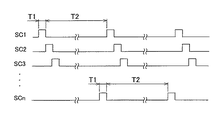
【図5】走査線を選択するためのタイミングチャート。
【図6】電気光学装置を携帯電話に具体化した構成を示す斜視図。
【符号の説明】
ΔR,ΔG,ΔB…偏差、BD…画像データ、K1,K2,K3…増幅率、C1…保持キャパシタ、Qd…駆動トランジスタ、Qsw…スイッチングトランジスタ、SR,SG,SB…検出信号、VR,VG,VB…電源電圧、Y1〜Yn…走査線、X1〜Xm…データ線、Z1…画像表示領域、Z2…光検知領域、ΔVR,ΔVG,ΔVB…補正値、ΔVRa,ΔVGa,ΔVBa…補正値(平均補正値)、VCR,VCG,VCB…目標輝度電圧、VSR,VSG,VSB…検出電圧、VL…電源線、VRdata,VGdata,VBdata…データ電圧、10…電気光学装置としての有機ELディスプレイ、11…表示パネル部、12…データ線駆動回路、13…走査線駆動回路、15…電源供給回路、16…モニタ回路、17…制御回路、20R,20G,20B…画素回路、21…電気光学素子又はEL素子としての有機EL素子、22…光検知素子、32R,32G,32B…目標電圧生成回路、80…電子機器としての携帯電話。[0001]
TECHNICAL FIELD OF THE INVENTION
The present invention relates to an electro-optical device and an electronic device.
[0002]
[Prior art]
2. Description of the Related Art Conventionally, electro-optical devices such as liquid crystal display devices and organic EL display devices are mounted on electronic devices such as mobile phones and PDAs. Electro-optical devices are required to always maintain a constant luminance for image data in order to maintain display quality.
[0003]
However, it is known that the luminance due to the deterioration of the electro-optical element decreases when the device is used for a long time. In addition, the brightness of the image data decreases during a period from the start of driving to the elapse of a predetermined time (time until stabilization).
[0004]
Therefore, it has been proposed to improve the manufacturing method in order to prevent a decrease in luminance (see
[0005]
[Patent Document 1]
JP-A-11-154596
[Patent Document 2]
JP-A-11-214157
[0006]
[Problems to be solved by the invention]
By the way, as described above, since the factors of the luminance variation are various, in order to satisfy all of them, it is necessary to detect all the individual factors and control the luminance of the electro-optical element based on these factors. As a result, the control method becomes complicated and the circuit scale becomes large.
[0007]
SUMMARY An advantage of some aspects of the invention is that an electro-optical device and an electronic apparatus which can adjust luminance fluctuation with a simple configuration regardless of a factor of luminance fluctuation. To provide.
[0008]
[Means for Solving the Problems]
The electro-optical device according to the present invention includes a plurality of scanning lines, a plurality of data lines, a plurality of electro-optical elements provided in a matrix between the plurality of scanning lines and the plurality of data lines, A power supply line for supplying drive power to each of the electro-optical elements, and an electro-optical device that drives the electro-optical element according to an electric signal supplied via the data line based on image data, At least one of the plurality of electro-optical elements is used as a monitoring electro-optical element, and a light detecting element for detecting light emitted from the monitoring electro-optical element; The drive power supplied to the electro-optical element from the power supply line is corrected based on a value of a target detection signal prepared in advance and a value of an actual detection signal from the light detecting element to be output to the electro-optical element. And a monitor circuit for obtaining a correction value of the order.
[0009]
According to this, the light emitted from the monitoring electro-optical element is detected by the light detecting element, and the detection signal is output to the monitor circuit. The monitor circuit is a drive power supply that supplies power to the electro-optical element from a power supply line based on a value of a target detection signal to be output for image data from the light detection element and a value of an actual detection signal from the light detection element. A correction value for correcting is calculated. Therefore, the fluctuation of the luminance with respect to the image data can be suppressed only by adjusting the driving power supply regardless of the factor of the fluctuation of the luminance.
[0010]
In this electro-optical device, a plurality of scanning lines, a plurality of data lines, a plurality of electro-optical elements, and a power supply line are provided on a display panel substrate, and the monitor electro-optical element is provided in a display area on the display panel substrate. It is formed outside.
According to this, since the monitor electro-optical element is formed outside the display area on the display panel substrate, it does not hinder image display.
[0011]
In the electro-optical device, the monitor circuit receives the image data, and outputs a target detection signal value to be output from the light detection element to the image data. A comparison circuit for comparing a value of an actual detection signal from an element with a value of a target detection signal from the target voltage generation circuit to obtain a deviation value; and the power supply based on the deviation value obtained by the comparison circuit. A correction circuit for obtaining a correction value for correcting a voltage value of a driving power supply supplied to the electro-optical element from the line.
[0012]
According to this, the comparison circuit compares the value of the target detection signal to be output from the light detection element and the value of the actual detection signal from the light detection element with respect to the current image data from the target voltage generation circuit. Compare and find the deviation value. The correction circuit obtains a correction value for correcting the voltage value of the driving power supply supplied to the electro-optical element from the power supply line based on the deviation value. Accordingly, since the deviation value is obtained and the correction value is obtained based on the deviation value, the configuration for suppressing the fluctuation of the luminance with respect to the image data is a very simple configuration.
[0013]
The electro-optical device includes a power supply circuit that corrects a power supply voltage supplied to the power supply line at that time to a new power supply voltage based on a correction value obtained by the monitor circuit.
According to this, the power supply circuit supplies a new power supply voltage to each electro-optical element based on the correction value to suppress a change in luminance with respect to the image data.
[0014]
In the electro-optical device, at least one monitoring electro-optical element is provided for each of the plurality of scanning lines, and the correction value obtained based on each monitoring electro-optical element for each scanning line is provided. And a control circuit for obtaining an average value from the power supply circuit and outputting the average value as an average correction value to the power supply circuit.
[0015]
According to this, a new power supply voltage is obtained from the average value of the correction values obtained based on the monitor electro-optical elements. The effect of the correction value of the unit can be reduced.
[0016]
In this electro-optical device, at least one monitoring electro-optical element is provided for each of the plurality of data lines, and the correction value obtained based on each monitoring electro-optical element for each data line is provided. And a control circuit for obtaining an average value from the power supply circuit and outputting the average value as an average correction value to the power supply circuit.
[0017]
According to this, a new power supply voltage is obtained from the average value of the correction values obtained based on the monitor electro-optical elements. The effect of the correction value of the unit can be reduced.
[0018]
In this electro-optical device, a plurality of electro-optical elements, a plurality of types of electro-optical elements having different optical characteristics are alternately arranged on each scanning line, and each electro-optical element corresponds to each of the optical characteristics. A drive power supply is supplied to drive.
[0019]
According to this, the correction value is obtained for each electro-optical element having different optical characteristics, and the drive power supply is adjusted for each electro-optical element having different optical characteristics.
[0020]
In this electro-optical device, the electro-optical element is an EL element.
According to this, the fluctuation of the luminance of the EL element can be suppressed by adjusting the driving power supply.
[0021]
In this electro-optical device, the EL element has a light-emitting layer made of an organic material.
According to this, the fluctuation of the luminance of the organic EL element is suppressed by adjusting the driving power supply.
[0022]
The electronic apparatus according to the present invention has the above-described electro-optical device mounted thereon.
According to this, the fluctuation of the luminance can be adjusted irrespective of the factor of the fluctuation of the luminance, and the image can be displayed at the luminance corresponding to the image data, so that the display quality is high.
[0023]
BEST MODE FOR CARRYING OUT THE INVENTION
(1st Embodiment)
Hereinafter, a first embodiment of the present invention will be described with reference to FIGS.
[0024]
FIG. 1 is a block circuit diagram showing a circuit configuration of an
[0025]
1, the
[0026]
The
[0027]
In the
[0028]
As shown in FIG. 2, a
[0029]
Each of the
[0030]
In the present embodiment, the regions where the pixel circuits (display pixel circuits) 20R, 20G, and 20B connected between the data lines X1 to Xm-3 and the scanning lines Y1 to Yn are formed. The image display area Z1 is set. A region where each of the pixel circuits (monitor pixel circuits) 20R, 20G, and 20B connected between the data lines Xm-2 to Xm and the scanning lines Y1 to Yn is defined as a light detection region Z2. I have.
[0031]
Each of the
[0032]
FIG. 3 is a circuit diagram showing an electrical configuration of each of the
[0033]
The drive transistor Qd has a source connected to the anode of the organic EL element (organic EL element for display) 21 and a drain connected to the drive power supply line VL. The holding capacitor C1 is connected between the gate of the driving transistor Qd and the driving power supply line VL.
[0034]
In the present embodiment, the drive power supply line VL includes a red drive power supply line VLR, a green drive power supply line VLG, and a blue drive power supply line VLB. The driving transistor Qd of the
[0035]
This is because the characteristics of the
[0036]
The gates of the switching transistors Qsw of the
[0037]
That is, a red data signal (data voltage VRdata) is output from the data
[0038]
Note that the
[0039]
Next, the operation of each
[0040]
Now, when the H-level scanning signal SCn is output from the scanning
[0041]
Similarly, in FIG. 4, the
[0042]
The data voltages VRdata, VGdata, and VBdata are supplied to the holding capacitor C1 via the turned-on switching transistors Qsw. Each holding capacitor C1 is charged to a charge amount having a value corresponding to the level of each of the supplied data voltages VRdata, VGdata, and VBdata. Then, even if the scanning signal SCn at the H level becomes L level after the predetermined period T1 has elapsed and the switching transistor Qsw is turned off, the charge amount corresponding to the data voltages VRdata, VGdata, and VBdata respectively remains in the holding capacitor C1. Is held. When the charge corresponding to the data voltages VRdata, VGdata, and VBdata is held, the drive transistor Qd is turned on according to the charge, and supplies the drive current Ioel to the
[0043]
The drive transistor Qd of each of the
[0044]
The data
[0045]
That is, in the present embodiment, one
[0046]
For example, assuming that there are 32 brightness gradations, data voltages VRdata, VGdata, and VBdata of 32 levels are respectively generated, and the data voltages VRdata, VGdata, and VBdata of the levels corresponding to the gradations are driven by the data lines. The signals are output from the
[0047]
Further, the data
[0048]
The scanning
[0049]
The
[0050]
The
[0051]
In the present embodiment, when one of the n detection circuit units ends the detection (sampling) operation, the next detection circuit unit performs the sampling operation. The sampling operation is performed in order from the detection circuit unit for the scanning line Y1 to the scanning line Yn, and returns to the scanning line Y1 to repeat the same selection operation as before. In addition, the sampling periods and the sampling start timings of the n detection circuit units are determined in advance. The sampling operation of each detection circuit of the
[0052]
In the present embodiment, the sampling period is set to coincide with a so-called light emission period T2 in which a new H-level scanning signal SCn is output after the H-level scanning signal SCn falls to the L level. The sampling start timing of each detection circuit unit is as follows. In other words, when the detection unit for the previous scanning line is selected and the sampling operation is being performed, the timing at which the detection circuit unit for the next scanning line is selected is a period during which all the scanning lines have been selected in one cycle. (One vertical scanning period (= T1 + T2) is the time when the scanning line is selected and the light emitting period T2 starts.
[0053]
Therefore, every time the n frames are displayed as an image, the n detection circuit units constituting the
In FIG. 4, a detection circuit unit constituting the
[0054]
The
[0055]
The target
[0056]
The map data built in the target
[0057]
The green target
[0058]
Further, the target
[0059]
The
[0060]
The
[0061]
In the present embodiment, the amplification factors k1, k2, and k3 of the
[0062]
The
[0063]
Further, the
[0064]
The
[0065]
Next, the operation of the
As shown in FIG. 5, when the H-level scanning signal SC1 is output to the scanning line Y1 for a predetermined period T1, the switching transistors Qsw of all the
[0066]
When the scanning line Y1 shifts to non-selection (the scanning signal SC1 is at L level), the scanning signal SC2 at H level is output to the scanning line Y2 for a certain period T1, and the next scanning line Y2 is selected (selection period). Then, similarly to the above, the data voltages VRdata, VGdata, VBdata based on the image data BD are supplied to the
[0067]
When the selection of all the scanning lines Y1 to Yn makes one cycle, an image of one frame is displayed. Then, by repeating such an operation based on the image data BD, a new one-frame image is displayed in the image display area Z1.
[0068]
On the other hand, when an image of one frame is displayed in the image display area Z1, the
[0069]
That is, in the detection circuit section of the
[0070]
That is, during the period of generating the image of the first one frame, the
[0071]
Then, each time the image of 60 frames is displayed, the correction values ΔVR, ΔVG, ΔVB output from the n detection circuit units make one cycle. When each of the n correction values ΔVR, ΔVG, ΔVB is input, the
[0072]
Thereafter, the
[0073]
Therefore, when an image is continuously displayed based on the image data BD, when the luminance of the
[0074]
Next, features of the
(1) According to the present embodiment, when the luminance of the
[0075]
(2) In the present embodiment, when the luminance of the
[0076]
(3) In the present embodiment, by detecting the
[0077]
In addition, an average value is obtained from the n correction values ΔVR, ΔVG, ΔVB obtained from the n
[0078]
(4) In the present embodiment, the power supply voltages VR, VG, and VB are independently controlled for each color, so that it is not necessary to consider the power supply voltages of other colors, so that the control is facilitated.
[0079]
(5) In the present embodiment, since the
[0080]
(2nd Embodiment)
Next, application of the
[0081]
FIG. 6 is a perspective view showing a configuration of a mobile phone. In FIG. 6, a
[0082]
Note that the embodiment of the present invention may be modified as follows.
In the first embodiment, each of the
[0083]
In the first embodiment, the
[0084]
In the above-described embodiment, the organic EL display is provided with the
[Brief description of the drawings]
FIG. 1 is a block circuit diagram showing a circuit configuration of an
FIG. 2 is a circuit diagram showing an internal circuit configuration of a display panel unit.
FIG. 3 is a circuit diagram showing an internal circuit configuration of a pixel circuit in an image display area.
FIG. 4 is a circuit diagram showing an internal circuit configuration of a monitor pixel circuit and a detection circuit.
FIG. 5 is a timing chart for selecting a scanning line.
FIG. 6 is a perspective view showing a configuration in which the electro-optical device is embodied in a mobile phone.
[Explanation of symbols]
ΔR, ΔG, ΔB: deviation, BD: image data, K1, K2, K3: amplification factor, C1: holding capacitor, Qd: driving transistor, Qsw: switching transistor, SR, SG, SB: detection signal, VR, VG, VB: power supply voltage, Y1 to Yn: scanning line, X1 to Xm: data line, Z1: image display area, Z2: light detection area, ΔVR, ΔVG, ΔVB: correction value, ΔVRa, ΔVGa, ΔVBa: correction value (average Correction value), VCR, VCG, VCB: target luminance voltage, VSR, VSG, VSB: detection voltage, VL: power supply line, VRdata, VGdata, VBdata: data voltage, 10: organic EL display as an electro-optical device, 11 ... Display panel section, 12: data line drive circuit, 13: scanning line drive circuit, 15: power supply circuit, 16: monitor circuit, 17: control circuit , 20R, 20G, 20B ... pixel circuit, 21 ... organic EL element as an electro-optical element or an EL element, 22 ... light-sensing, 32R, 32G, 32B ... target voltage generation circuit, 80 ... mobile phone as an electronic apparatus.
Claims (10)
複数のデータ線と、
前記複数の走査線と前記複数のデータ線との間にマトリクス状に設けられた複数の電気光学素子と、
前記複数の電気光学素子にそれぞれ駆動電源を供給する電源線と
を含み、画像データに基づいて前記データ線を介して供給される電気信号に応じて前記電気光学素子を駆動させる電気光学装置であって、
前記複数の電気光学素子のうちの少なくとも1つをモニタ用の電気光学素子にし、そのモニタ用の電気光学素子から放たれる光を検知する光検知素子と、
前記光検知素子から前記画像データに対して出力されるべき予め用意された目標の検知信号の値と前記光検知素子からの実際の検知信号の値とに基づいて前記電源線から前記電気光学素子に供給する駆動電源を補正するための補正値を求めるモニタ回路と
を備えた電気光学装置。Multiple scan lines,
Multiple data lines,
A plurality of electro-optical elements provided in a matrix between the plurality of scanning lines and the plurality of data lines,
A power supply line for supplying drive power to each of the plurality of electro-optical elements, and an electro-optical device configured to drive the electro-optical elements in accordance with an electric signal supplied via the data lines based on image data. hand,
A light detection element for detecting at least one of the plurality of electro-optical elements as a monitor electro-optical element and detecting light emitted from the monitor electro-optical element,
The electro-optical element from the power supply line based on a value of a target detection signal prepared in advance to be output for the image data from the light detecting element and a value of an actual detection signal from the light detecting element. And a monitor circuit for obtaining a correction value for correcting the drive power supplied to the electro-optical device.
複数の走査線、複数のデータ線、複数の電気光学素子及び電源線は、表示パネル基板上に設けられ、
前記モニタ用の電気光学素子は、表示パネル基板上の表示領域外に形成されていることを特徴とする電気光学装置。The electro-optical device according to claim 1,
A plurality of scanning lines, a plurality of data lines, a plurality of electro-optical elements and a power supply line are provided on a display panel substrate,
The electro-optical device according to claim 1, wherein the monitor electro-optical element is formed outside a display area on a display panel substrate.
前記モニタ回路は、
前記画像データを入力しその画像データに対して前記光検知素子から出力されるべき目標の検知信号の値を出力する目標電圧生成回路と、
前記光検知素子からの実際の検知信号の値と前記目標電圧生成回路からの目標の検知信号の値とを比較し偏差値を求める比較回路と、
前記比較回路にて求めた前記偏差値に基づいて前記電源線から前記電気光学素子に供給する駆動電源の電圧値を補正するための補正値を求める補正回路と
を備えたことを特徴とする電気光学装置。The electro-optical device according to claim 1, wherein
The monitor circuit includes:
A target voltage generation circuit that inputs the image data and outputs a value of a target detection signal to be output from the light sensing element with respect to the image data;
A comparison circuit that compares a value of an actual detection signal from the light detection element with a value of a target detection signal from the target voltage generation circuit to obtain a deviation value;
A correction circuit for obtaining a correction value for correcting a voltage value of a drive power supply supplied to the electro-optical element from the power supply line based on the deviation value obtained by the comparison circuit. Optical device.
前記モニタ回路が求めた補正値に基づいてその時に前記電源線に供給している電源電圧を新たな電源電圧に補正する電源供給回路を備えたことを特徴とする電気光学装置。The electro-optical device according to any one of claims 1 to 3,
An electro-optical device comprising: a power supply circuit that corrects a power supply voltage supplied to the power supply line at that time to a new power supply voltage based on a correction value obtained by the monitor circuit.
前記複数の走査線に対して前記モニタ用の電気光学素子をそれぞれ少なくとも1つ設けるとともに、その各走査線のモニタ用の各電気光学素子に基づいて得られた前記補正値から平均値を求め、その平均値を平均補正値として前記電源供給回路に出力する制御回路を設けることを特徴とする電気光学装置。The electro-optical device according to any one of claims 1 to 4,
With at least one monitoring electro-optical element for each of the plurality of scanning lines, an average value is obtained from the correction values obtained based on the monitoring electro-optical elements for each scanning line, An electro-optical device comprising a control circuit for outputting the average value as an average correction value to the power supply circuit.
前記複数のデータ線に対して前記モニタ用の電気光学素子をそれぞれ少なくとも1つ設けるとともに、その各データ線のモニタ用の各電気光学素子に基づいて得られた前記補正値から平均値を求め、その平均値を平均補正値として前記電源供給回路に出力する制御回路を設けることを特徴とする電気光学装置。The electro-optical device according to any one of claims 1 to 4,
Along with providing at least one monitoring electro-optical element for each of the plurality of data lines, an average value is obtained from the correction values obtained based on the monitoring electro-optical elements for each data line, An electro-optical device comprising a control circuit for outputting the average value as an average correction value to the power supply circuit.
複数の電気光学素子は、光学的特性の異なる複数種類の電気光学素子が各走査線に交互に配置され、各電気光学素子に対してそれぞれの前記光学的特性に対応した駆動電源を供給して駆動させる電気光学装置。The electro-optical device according to any one of claims 1 to 6,
A plurality of electro-optical elements, a plurality of types of electro-optical elements having different optical characteristics are alternately arranged on each scanning line, and supply a driving power supply corresponding to the respective optical characteristics to each electro-optical element. An electro-optical device to be driven.
前記電気光学素子は、EL素子であることを特徴とする電気光学装置。The electro-optical device according to any one of claims 1 to 6,
The electro-optical device according to claim 1, wherein the electro-optical element is an EL element.
前記EL素子は、発光層が有機材料で構成されていることを特徴とする電気光学装置。The electro-optical device according to claim 8,
The electro-optical device according to claim 1, wherein the EL element has a light-emitting layer made of an organic material.
Priority Applications (1)
| Application Number | Priority Date | Filing Date | Title |
|---|---|---|---|
| JP2003051133A JP2004258489A (en) | 2003-02-27 | 2003-02-27 | Electrooptical device and electronic device |
Applications Claiming Priority (1)
| Application Number | Priority Date | Filing Date | Title |
|---|---|---|---|
| JP2003051133A JP2004258489A (en) | 2003-02-27 | 2003-02-27 | Electrooptical device and electronic device |
Publications (1)
| Publication Number | Publication Date |
|---|---|
| JP2004258489A true JP2004258489A (en) | 2004-09-16 |
Family
ID=33116355
Family Applications (1)
| Application Number | Title | Priority Date | Filing Date |
|---|---|---|---|
| JP2003051133A Pending JP2004258489A (en) | 2003-02-27 | 2003-02-27 | Electrooptical device and electronic device |
Country Status (1)
| Country | Link |
|---|---|
| JP (1) | JP2004258489A (en) |
Cited By (8)
| Publication number | Priority date | Publication date | Assignee | Title |
|---|---|---|---|---|
| JP2006201751A (en) * | 2004-12-21 | 2006-08-03 | Seiko Epson Corp | Light emitting device, image forming apparatus, display, and driving method for light emitting element |
| JP2006267766A (en) * | 2005-03-25 | 2006-10-05 | Quanta Display Inc | Active matrix organic light emitting diode driving control circuit with capability of dynamically adjusting white balance and adjustment method thereof |
| JP2007171507A (en) * | 2005-12-21 | 2007-07-05 | Sony Corp | Spontaneous light emission display device, conversion table updating device, and program |
| JP2007286341A (en) * | 2006-04-17 | 2007-11-01 | Eastman Kodak Co | Display device |
| EP1978504A2 (en) * | 2007-04-06 | 2008-10-08 | Samsung SDI Co., Ltd. | Organic light emitting diode (OLED) display and a method of driving the same |
| JP2008268437A (en) * | 2007-04-18 | 2008-11-06 | Hitachi Displays Ltd | Organic el display |
| CN100452159C (en) * | 2004-12-31 | 2009-01-14 | 乐金显示有限公司 | Driving system for an electro-luminescent display device |
| WO2019187085A1 (en) * | 2018-03-30 | 2019-10-03 | シャープ株式会社 | Display device and manufacturing method therefor |
-
2003
- 2003-02-27 JP JP2003051133A patent/JP2004258489A/en active Pending
Cited By (10)
| Publication number | Priority date | Publication date | Assignee | Title |
|---|---|---|---|---|
| JP2006201751A (en) * | 2004-12-21 | 2006-08-03 | Seiko Epson Corp | Light emitting device, image forming apparatus, display, and driving method for light emitting element |
| CN100452159C (en) * | 2004-12-31 | 2009-01-14 | 乐金显示有限公司 | Driving system for an electro-luminescent display device |
| JP2006267766A (en) * | 2005-03-25 | 2006-10-05 | Quanta Display Inc | Active matrix organic light emitting diode driving control circuit with capability of dynamically adjusting white balance and adjustment method thereof |
| JP2007171507A (en) * | 2005-12-21 | 2007-07-05 | Sony Corp | Spontaneous light emission display device, conversion table updating device, and program |
| JP2007286341A (en) * | 2006-04-17 | 2007-11-01 | Eastman Kodak Co | Display device |
| EP1978504A2 (en) * | 2007-04-06 | 2008-10-08 | Samsung SDI Co., Ltd. | Organic light emitting diode (OLED) display and a method of driving the same |
| EP1978504B1 (en) * | 2007-04-06 | 2015-04-22 | Samsung Display Co., Ltd. | Organic light emitting diode (OLED) display and a method of driving the same |
| JP2008268437A (en) * | 2007-04-18 | 2008-11-06 | Hitachi Displays Ltd | Organic el display |
| WO2019187085A1 (en) * | 2018-03-30 | 2019-10-03 | シャープ株式会社 | Display device and manufacturing method therefor |
| US11250789B2 (en) | 2018-03-30 | 2022-02-15 | Sharp Kabushiki Kaisha | Display device and manufacturing method therefor |
Similar Documents
| Publication | Publication Date | Title |
|---|---|---|
| US10796622B2 (en) | Display system with compensation techniques and/or shared level resources | |
| US10319307B2 (en) | Display system with compensation techniques and/or shared level resources | |
| KR101509118B1 (en) | Organic light emitting device, and apparatus and method of generating modification information therefor | |
| KR101861795B1 (en) | Luminance Correction System for Organic Light Emitting Display Device | |
| US20060092183A1 (en) | System and method for setting brightness uniformity in an active-matrix organic light-emitting diode (OLED) flat-panel display | |
| US8624942B2 (en) | Luminance correction system for organic light emitting display | |
| US10607537B2 (en) | Systems and methods of optical feedback | |
| KR101276456B1 (en) | Organic el display device and method for manufacturing the same | |
| US20050088379A1 (en) | Image display apparatus | |
| CN108022557B (en) | Data driver and display device using the same | |
| KR20090063207A (en) | Oled luminance degradation compensation | |
| JP2004354635A (en) | Electrooptical apparatus, driving method of electrooptical apparatus, and electronic equipment | |
| TWI751573B (en) | Light emitting display device and method for driving same | |
| JP2003255900A (en) | Color organic el display device | |
| US20110141097A1 (en) | Organic light emitting display device and driving voltage correction method thereof | |
| US11984076B2 (en) | Display panel compensation methods | |
| KR20080096399A (en) | Display correction circuit of an organic el panel | |
| US11222597B2 (en) | Display device and method for controlling same | |
| KR100820719B1 (en) | Method of Driving Organic Electroluminescent Display To Compensate Brightness of Bad Pixel thereof and Organic Electroluminescent Display used in the same | |
| JP2004258489A (en) | Electrooptical device and electronic device | |
| US20070229410A1 (en) | Display apparatus | |
| US20090184900A1 (en) | Image display device and display device control method | |
| KR102281009B1 (en) | Orgainc emitting diode display device and method for driving the same | |
| US20130241966A1 (en) | El display device | |
| JP2011164425A (en) | Image display device |
Legal Events
| Date | Code | Title | Description |
|---|---|---|---|
| A621 | Written request for application examination |
Free format text: JAPANESE INTERMEDIATE CODE: A621 Effective date: 20060220 |
|
| RD04 | Notification of resignation of power of attorney |
Free format text: JAPANESE INTERMEDIATE CODE: A7424 Effective date: 20070403 |
|
| A977 | Report on retrieval |
Free format text: JAPANESE INTERMEDIATE CODE: A971007 Effective date: 20091110 |
|
| A131 | Notification of reasons for refusal |
Free format text: JAPANESE INTERMEDIATE CODE: A131 Effective date: 20091117 |
|
| A521 | Request for written amendment filed |
Free format text: JAPANESE INTERMEDIATE CODE: A523 Effective date: 20100113 |
|
| RD03 | Notification of appointment of power of attorney |
Free format text: JAPANESE INTERMEDIATE CODE: A7423 Effective date: 20100113 |
|
| A02 | Decision of refusal |
Free format text: JAPANESE INTERMEDIATE CODE: A02 Effective date: 20100223 |