JP2004251969A - Phase shift mask, method for forming pattern by using phase shift mask, and method for manufacturing electronic device - Google Patents
Phase shift mask, method for forming pattern by using phase shift mask, and method for manufacturing electronic device Download PDFInfo
- Publication number
- JP2004251969A JP2004251969A JP2003039582A JP2003039582A JP2004251969A JP 2004251969 A JP2004251969 A JP 2004251969A JP 2003039582 A JP2003039582 A JP 2003039582A JP 2003039582 A JP2003039582 A JP 2003039582A JP 2004251969 A JP2004251969 A JP 2004251969A
- Authority
- JP
- Japan
- Prior art keywords
- pattern
- phase shift
- shift mask
- light
- opening
- Prior art date
- Legal status (The legal status is an assumption and is not a legal conclusion. Google has not performed a legal analysis and makes no representation as to the accuracy of the status listed.)
- Pending
Links
Images


Classifications
-
- G—PHYSICS
- G03—PHOTOGRAPHY; CINEMATOGRAPHY; ANALOGOUS TECHNIQUES USING WAVES OTHER THAN OPTICAL WAVES; ELECTROGRAPHY; HOLOGRAPHY
- G03F—PHOTOMECHANICAL PRODUCTION OF TEXTURED OR PATTERNED SURFACES, e.g. FOR PRINTING, FOR PROCESSING OF SEMICONDUCTOR DEVICES; MATERIALS THEREFOR; ORIGINALS THEREFOR; APPARATUS SPECIALLY ADAPTED THEREFOR
- G03F7/00—Photomechanical, e.g. photolithographic, production of textured or patterned surfaces, e.g. printing surfaces; Materials therefor, e.g. comprising photoresists; Apparatus specially adapted therefor
- G03F7/20—Exposure; Apparatus therefor
-
- G—PHYSICS
- G03—PHOTOGRAPHY; CINEMATOGRAPHY; ANALOGOUS TECHNIQUES USING WAVES OTHER THAN OPTICAL WAVES; ELECTROGRAPHY; HOLOGRAPHY
- G03F—PHOTOMECHANICAL PRODUCTION OF TEXTURED OR PATTERNED SURFACES, e.g. FOR PRINTING, FOR PROCESSING OF SEMICONDUCTOR DEVICES; MATERIALS THEREFOR; ORIGINALS THEREFOR; APPARATUS SPECIALLY ADAPTED THEREFOR
- G03F1/00—Originals for photomechanical production of textured or patterned surfaces, e.g., masks, photo-masks, reticles; Mask blanks or pellicles therefor; Containers specially adapted therefor; Preparation thereof
- G03F1/26—Phase shift masks [PSM]; PSM blanks; Preparation thereof
- G03F1/32—Attenuating PSM [att-PSM], e.g. halftone PSM or PSM having semi-transparent phase shift portion; Preparation thereof
Landscapes
- Physics & Mathematics (AREA)
- General Physics & Mathematics (AREA)
- Preparing Plates And Mask In Photomechanical Process (AREA)
- Exposure And Positioning Against Photoresist Photosensitive Materials (AREA)
Abstract
Description
【0001】
【発明の属する技術分野】
本発明は、ハーフトーン型の位相シフトマスク、その位相シフトマスクを用いたパターンの形成方法および電子デバイスの製造方法に関するものである。
【0002】
【従来の技術】
近年、半導体集積回路における高集積化および微細化には目覚しいものがある。それに伴い、半導体基板(以下、単にウェハと称する)上に形成される回路パターンの微細化も急速に進んできている。
【0003】
中でも、フォトリソグラフィ技術がパターン形成における基本技術として広く認識されるところである。よって、今日までに種々の開発、改良がなされてきている。しかし、パターンの微細化はとどまるところを知らず、パターンの解像度向上への要求もさらに強いものとなってきている。
【0004】
このフォトリソグラフィ技術とは、ウェハ上に塗布されたフォトレジストにフォトマスク(原画)上のパターンを転写し、その転写されたフォトレジストを用いて下層の被エッチング膜をパターニングする技術である。
【0005】
このフォトレジストの転写時においては、フォトレジストに現像処理が施されるが、この現像処理によって光の当った部分のフォトレジストが除去されるタイプをボジ型、光の当らない部分のフォトレジストが除去されるタイプをネガ型のフォトレジストという。
【0006】
一般に、縮小露光方法を用いたフォトリソグラフィ技術における解像限界R(nm)は、
R=k1・λ/(NA)
と表わされる。ここで、λは使用する光の波長(nm)、NAはレンズの投影光学系の開口数、k1は結像条件およびレジストプロセスに依存する定数である。
【0007】
上式からわかるように、解像限界Rの向上を図るためには、すなわち微細パターンを得るためには、k1とλとの値を小さくし、NAの値を大きくする方法が考えられる。つまり、レジストプロセスに依存する定数を小さくするとともに、短波長化や高NA化を進めればよいのである。
【0008】
これらのうち、光源の短波長化は技術的に難しく、同一波長での高NA化によることが必要となっている。しかし、高NA化を進めると、光の焦点深度δ(δ=k2・λ/(NA)2)が浅くなり、形成パターンの形状、寸法精度の劣化を招くといった問題がある。
【0009】
そこで、光源やレンズではなく、フォトマスクを改良することにより、パターンの微細化を図る研究がなされている。最近では、パターンの解像度を向上させるフォトマスクとして位相シフトマスクが注目されている。
【0010】
このような位相シフトマスクとして、たとえば半透明位相シフト部と透過部とを最適な寸法の組合わせで構成することにより、実効的な暗部を形成するものが特開平10−293392号公報に開示されている。
【0011】
【特許文献1】
特開平10−293392号公報
【0012】
【発明が解決しようとする課題】
しかしながら、従来の位相シフトマスクを用いてホールパターンを形成する場合において、特に露光波長よりも小さい寸法のパターンを形成するときには、マスク寸法の微細な変化がウェハに形成されるレジストパターンの寸法の大きな変化として反映される。このため、所望の寸法のホールパターンを形成することが困難になるという問題がある。つまり、非常に寸法誤差の小さいマスクパターンが必要となるため、マスク製造に高度な技術が要求され、マスクコストが大きくなるという問題があった。
【0013】
また、従来のホールパターン形成方法で形成されたパターンでは寸法不均一による半導体集積回路製造における歩留まりの低下や、これを避けるためにパターン配置間隔を大きくすると、集積度が低下するという問題があった。
【0014】
また、パターンの寸法の不均一そのものを解消するためには高度のマスクが必要となり、高コストとなるという問題があった。
【0015】
本発明は、上記のような問題を解決するためになされたものであって、集積度を低下させることなく、かつ低コストで、寸法均一性に優れたパターンを形成できる位相シフトマスク、その位相シフトマスクを用いたパターンの形成方法および電子デバイスの製造方法を提供することである。
【0016】
【課題を解決するための手段】
本発明の位相シフトマスクは、露光光を透過する材質よりなる基板と、その基板上に形成されかつ基板の一部表面を露出する開口部を有するハーフトーン遮光膜とを備えている。ハーフトーン遮光膜を透過した露光光の位相は開口部を透過した露光光の位相と異なっている。開口部を透過した露光光の光強度に対するハーフトーン遮光膜を透過した露光光の光強度の比により定義される光透過率は15%以上25%以下である。開口部の寸法は、露光光の波長λ/開口数NAを1とした計測で0.26以上0.45以下である。
【0017】
【発明の実施の形態】
以下、本発明の実施の形態について図に基づいて説明する。
【0018】
図1は、本発明の実施の形態1における位相シフトマスクの構成を概略的に示す断面図である。図1を参照して、位相シフトマスク5は、透明基板1と、ハーフトーン遮光膜2とを有している。透明基板1は、露光光を透過するように露光光に対して透明な材質よりなっている。ハーフトーン遮光膜2は、透明基板1上に形成され、かつ透明基板1の一部表面を露出する開口部2aを有している。
【0019】
ハーフトーン遮光膜2は、そのハーフトーン遮光膜2を透過した露光光の位相が開口部2aを透過した露光光の位相と異なる位相(たとえば180°異なる位相)となるように構成されている。また、開口部2aを透過した露光光の光強度I1に対するハーフトーン遮光膜2を透過した露光光の光強度I2の比(I2/I1)により定義される光透過率が15%以上25%以下である。また、開口部2aの寸法Wが、露光光の波長(λ)/開口数(NA)を1とした計測で0.26以上0.45以下である。
【0020】
ここで、開口部2aの寸法Wとは、開口部2aの平面形状が矩形状である場合には、その矩形の1辺の寸法を意味する。
【0021】
次に図1に示す位相シフトマスクを用いたパターンの形成方法について説明する。
【0022】
図2は、本発明の一実施の形態における位相シフトマスクを用いた投影露光装置の構成を概略的に示す図である。図2を参照して、この投影露光装置は、位相シフトマスク5上のパターンを縮小してウェハ20表面のフォトレジスト23に投射するものである。また投影露光装置は、光源11から位相シフトマスク5のパターンまでの照明光学系と、位相シフトマスク5のパターンからウェハ20までの投影光学系とを有している。
【0023】
照明光学系は、光源である水銀ランプ11と、反射鏡12と、集光レンズ18と、フライアイレンズ13と、絞り14と、集光レンズ16a、16b、16cと、ブラインド絞り15と、反射鏡17とを有している。また投影光学系は投影レンズ19a、19bと、瞳面絞り25とを有している。
【0024】
その露光動作においては、まず水銀ランプ11から発せられた光11aは、反射鏡12により、たとえばi線(波長365nm)のみが反射されて、単波長の光となる。次に、光11aは、集光レンズ18を通過して、フライアイレンズ13の各フライアイ構成レンズ13aの各々に入射し、その後に絞り14を通過する。
【0025】
ここで、光11bは、1個のフライアイ構成レンズ13aによって作り出された光路を示し、光11cはフライアイレンズ13によって作り出される光路を示している。
【0026】
絞り14を通過した光11aは、集光レンズ16a、ブラインド絞り15および集光レンズ16bを通過して、反射鏡17により所定角度で反射される。
【0027】
反射鏡17により反射された光11aは、集光レンズ16cを透過した後、所定のパターンが形成された位相シフトマスク5の全面を均一に照射する。この後、光11aは投影レンズ19a、19bにより所定の倍率に縮小され、ウェハ20表面のフォトレジスト23を露光する。
【0028】
本実施の形態においては、位相シフトマスク5の照明は通常照明ではなく、変形照明により行なわれる。通常照明の場合、図3に示すように位相シフトマスク5に対して露光光が垂直に照射され、0次光および±1次光の3光束によりウェハ20が露光される。しかし、位相シフトマスク5のパターンが微細になると、回折角度が大きくなるため、垂直照明では±1次光がレンズの中に入らなくなり、解像しなくなるおそれがある。
【0029】
そこで、図4に示すように変形照明により照明光束が位相シフトマスク5に対して斜めに入射される。これにより、位相シフトマスク5により回折した0次光と+1次光あるいは−1次光の2光束のみで露光することができ、解像性を得ることができる。
【0030】
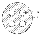
この変形照明においては、図5に示すように4つの透過部14aを有するクロスポール照明絞りや、図6に示すように輪状の透過部14aを有する輪帯照明絞りや、図7に示すように4つの透過部14aを有し、かつクロスポール照明を45°回転した形状を有する4重極照明絞りが、図2の絞り14として用いられてもよい。これにより、変形照明としてクロスポール照明や、輪帯照明や、4重極照明を実現することができる。
【0031】
なお、クロスポール照明を用いた場合には、ウェハ面内のX、Y座標での直交格子上に配置される高密集パターンの配置が可能となる。また、輪帯照明を用いた場合には、パターン配置依存性の小さい汎用的なパターン形成が可能となる。また、4重極照明を用いた場合には、ウェハ面内のX、Y座標において、クロスポール照明で形成したパターン配置に対して45°回転した状態での直交格子上に配置される高密集パターンの配置が可能となる。
【0032】
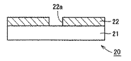
図8を参照して、このような変形照明により位相シフトマスク5を照明した露光光によりウェハ20表面のフォトレジスト23が露光される。露光されたフォトレジスト23は現像によりパターニングされる。この現像において、フォトレジスト23がネガ型の場合には、図9に示すように所定の値以下の露光エネルギが入力された部分のフォトレジスト23のみが除去されて、フォトレジスト23がパターニングされる。このパターニングされたフォトレジスト23をマスクとして、下層の被エッチング膜22をエッチングすることにより、その被エッチング膜22にホールパターン22aを形成することができる。この後、フォトレジスト23がたとえばアッシングなどにより除去されて、図10に示すように微細なホールパターン22aを有する被エッチング膜22が半導体基板21上に形成された半導体装置を製造することができる。
【0033】
また、上記の現像において、フォトレジスト23がポジ型の場合には、図11に示すように所定の値以上の露光エネルギが入力された部分のフォトレジスト23のみが除去されて、フォトレジスト23がパターニングされる。このパターニングされたフォトレジスト23をマスクとして、下層の被エッチング膜22をエッチングすることにより、その被エッチング膜22をドットパターンに形成することができる。この後、フォトレジスト23がたとえばアッシングなどにより除去されて、図12に示すように微細なドットパターンよりなる被エッチング膜22が半導体基板21上に形成された半導体装置を製造することができる。
【0034】
なお、フォトレジスト23がネガ型およびポジ型のいずれの場合においても、フォトレジスト23の露光は、開口径が波長λ/開口数NAを1とした計測で10以上の寸法の大きい開口パターンで、フォトレジスト23が感光して溶解性が反転する遷移露光量の10倍以上40倍以下の露光量で行われることが好ましい。なぜなら、これ以外の範囲の露光量では、良好な解像性を得ることが難しいからである。
【0035】
本実施の形態の位相シフトマスクによれば、マスクに形成されたパターン(開口部2a)の寸法変動に対するフォトレジストに形成されたパターン(ホールパターン:図9、ドットパターン:図11)の寸法変動(MEF:mask error enhancement factor)を小さくすることができる。以下、そのことを説明する。
【0036】
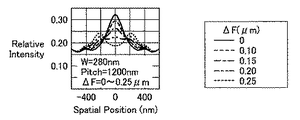
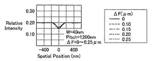
図13〜図16は、図1に示す位相シフトマスク5の開口部2aを孤立パターンとし、その孤立パターン2aの寸法Wに対して結像系により形成される光学像の変化を示す図である。各グラフでのパラメータはフォーカスである。光学条件として、露光光の波長は248nm、開口数NAは0.80、照明はクロスポール照明(σin/σout=0.70/0.85)である。そのクロスポール照明の絞り14の形状は図17に示すような4つの光透過部14aを有する形状である、また、位相シフトマスク5の透過率(I2/I1)は20%である。
【0037】
位相シフトマスク5の開口部の寸法Wが大きいときには、従来のハーフトーン型位相シフトマスクによるパターン形成の場合にほぼ対応する。この場合、図13に示すように開口部2aの透過光の強度が、それを打ち消す位相関係となるハーフトーン遮光膜2の透過光の強度に比べ十分に大きくなる。このため、開口部2aに対応する領域では、他の領域よりも明るい部分(光強度の高い部分)が形成される。
【0038】
開口部2aの寸法Wを小さくしていくと、図14に示すように開口部2aの透過光の強度が小さくなっていき、ハーフトーン遮光膜2の透過光による打消しが相対的に大きくなる。これにより、ハーフトーン遮光膜2の透過光の強度とほぼ同じ強度の像が形成されるようになる。このときは、像のコントラストが小さく、フォトレジストにパターンを形成することが困難となる。
【0039】
さらに開口部2aの寸法Wを小さくしていくと、開口部2aの透過光強度とハーフトーン遮光膜2の透過光強度とがほぼ等しくなる。このとき、相互の位相が反位相の関係(つまり位相が180°異なる関係)となっているので、図15に示すように、開口部2aに対応する領域では、他の領域よりも十分暗い点として像が形成される。この像をネガ型のフォトレジストに適用すれば、フォトレジストにホールパターンが形成されることになる。
【0040】
さらに開口部2aの寸法Wを小さくしていくと、図16に示すように、今度は開口部2aを透過した光の強度が、ハーフトーン遮光膜2の透過光の強度より小さくなり、打ち消しによる効果が小さくなることで、暗点の暗さが弱く(明るく)なっていく。
【0041】
さらに開口部2aの寸法Wを小さくしていくと、開口部2aが存在しないのと実質的に同じとなり、像のコントラストがなくなっていく。
【0042】
ここでの光学条件においては、図15に示すように暗点像が優れたフォーカス特性を示すことがわかる。
【0043】
上記より、ハーフトーン型の位相シフトマスクにおいて、開口部2aに対応する領域に形成される暗点像の暗さは、開口部2aのある寸法を境にして、その境界寸法よりも寸法を大きくしても小さくしても弱くなる(明るくなる)ことがわかる。
【0044】
図18は、図1に示す位相シフトマスクにおいて開口部の寸法W(mask width)を変化させたときの光学像変化を示す図である。図18の光学像変化より、上述したように光学像強度の極小値は、開口部2aのある寸法W(ここでは100〜120nm)で最小となり、開口部2aの寸法Wがそれより小さくても(80nm)、大きくても(140nm)、大きくなっていることがわかる。
【0045】
ある一定の露光量において、このように開口部2aの寸法Wの異なるマスクパターンをフォトレジストに露光すると、フォトレジストに形成されるパターンの寸法は、図中に示したスライスレベルの強度でフォトレジストの溶解/非溶解が分かれるとして、像がこのスライスレベルより小さくなる部分の寸法にほぼ一致する。すなわち、フォトレジストに形成されるパターンの寸法はマスクの開口部2aの寸法Wを大きくしても、小さくしても、小さくなることになる。特に、像強度の極小値が最小となる開口部2aの寸法Wにおいては、フォトレジストに形成されるパターンの寸法がその開口部2aの寸法Wに依存しなくなる(微分がゼロ)。
【0046】
図19は、前述したスライスレベルにより決定した像の寸法(フォトレジストに形成されたパターンの寸法:image CD)をマスクに形成された開口部2aの寸法(mask width)の関数としてプロットした図である。パラメータはスライスレベル(露光量に反比例する量)である。
【0047】
図19から明らかなように、像の寸法は、開口部2aのある寸法で極大となることが分かる。すなわち、開口部2aの寸法をこの極大となる値として、パターン形成を行なうと、開口部2aの寸法がマスク製造誤差により変動しても、像の寸法はほとんど変化しないようにすることができる。
【0048】
現時点のマスク製造技術の能力(state of art)では、開口部2aの寸法の製造誤差による分布は(×4マスクにおけるウェハ上換算値として)レンジで5nm以下である。このため、開口部2aの寸法を極大となる値とすれば、開口部2aの寸法が製造誤差により5nm変動しても、像の寸法の変化は極めて小さくなる(1〜2nm以下)ことがわかる。
【0049】
このようにマスクに形成されたパターンの寸法変動による像の寸法変動の割合は、MEF(mask error enhancement factor)と呼ばれ、以下の式で定義される。
【0050】
MEF=ΔCDウェハ/ΔCDマスク
この式において、「ΔCD(critical dimension)ウェハ」は像の寸法変動であり、「ΔCDマスク」はマスクに形成されたパターンのウエハ上に換算した寸法変動である。
【0051】
従来の方法により微細ホールパターンを形成するときには、このMEFの値が大きくなり、マスクに形成されたパターンのわずかな寸法変動が、像の寸法の大きな変動として反映され、本来一定の寸法であるべきパターンの寸法が大きく分布することとなる。これにより、デバイスの歩留まりや性能に悪影響が及ぶことは明らかであり、微細パターン形成における大きな問題となっている。
【0052】
これに対して本実施の形態では、開口部2aの寸法を80nm以上140nm以下にすることにより、上記のMEFを小さくすることができるため、開口部2aの寸法にほとんど影響を受けないパターンの形成が可能であり、優れた製造歩留まりや、デバイス性能を得ることができる。
【0053】
なお、開口部2aの寸法が100nm以上120nm以下であれば、開口部2aの寸法が製造誤差により5nm変動しても、像の寸法の変化を5nm程度と低く抑えることができるため好ましい。
【0054】
上記の開口部2aの寸法(80nm以上140nm以下、好ましくは100nm以上120nm以下)は、露光光の波長λが248nm、開口数NAが0.80の場合であるが、他の波長λおよび開口数NAの場合にもMEFを小さくできる適切な開口部2aの寸法がある。
【0055】
そこで、そのような適切な開口部の寸法を求めるために、波長λ/開口数NAを1として計測した場合の、開口部2aの寸法W0を以下の式より求めた。
【0056】
開口部2aの寸法:波長λ/開口数NA=80nm以上140nm以下:248/0.80=W0:1
上記より、(248/0.80)×W0=80nm以上140nm以下であるため、W0は0.26以上0.45以下となる。
【0057】
また開口部2aの寸法の好ましい範囲(100nm以上120nm以下)についても、上記と同様に、波長λ/開口数NAを1として計測した寸法W1に換算すると、その寸法W1は0.32以上0.39以下となる。
【0058】
以上より、各波長λおよび各開口数NAにおいて、その波長λ/開口数NAを1として計測した場合に、開口部2aの寸法が0.26以上0.45以下、好ましくは0.32以上0.39以下であれば、MEFを小さくすることが可能となる。
【0059】
なお、光透過率(I2/I1)が15%未満では図19中に示される曲線のカーブが急になり、MEFが大きくなってしまう。また、光透過率(I2/I1)が25%を超えると、位相シフトマスクの検査ができなくなってしまう。
【0060】
図20(a)、(b)および(c)の各々は、パターン汎用性を重視した光学条件下でのパターンピッチを変えたときの像寸法、MEFおよび焦点深度(DOF:depth of focus)のそれぞれの変化をプロットした図である。マスク寸法は120nmと一定であり、像寸法を一定にするためのマスクのパターン寸法の微調(いわゆる光近接効果補正(OPC:optical proximity correction))は行なっていない。
【0061】
図20(a)、(b)および(c)から分かるとおり、OPCを行なっていないので、パターンピッチの小さい密集部では像寸法が大きくなっているが、パターンピッチが極めて大きい孤立パターンからパターンピッチが300nmまでの範囲では、MEF<1、DOF>0.45でのパターンの形成が可能となる。
【0062】
なお、図20(a)、(b)および(c)での光学条件として、露光光の波長は248nm、開口数NAは0.80、照明はクロスポール照明(図13〜図16よりは弱い変形照明となっている)である。また、位相シフトマスク5の透過率(I2/I1)は20%である。
【0063】
さらに、本実施の形態の位相シフトマスクを用いたパターン形成方法によれば、マスクのパターン寸法およびスライスレベル(露光量)を調整することで、極めて密集したホールパターンを形成することが可能である。たとえば、本願発明者は、0.1μmルールのDRAM(Dynamic Random Access Memory)のストレージノードコンタクトのパターンの光学像についてフォーカスを変えた場合の変化を調べた。なお、近接ホールの中心間距離は200nmとした。
【0064】
その結果、ベストフォーカスからフォーカスが±0.3μmずれても良好な光学像を得ることができた。このことより、本実施の形態の位相シフトマスクを用いたパターン形成方法によれば、極めて密集したパターンにおいても、>0.6μmのDOFが得られることが分かった。
【0065】
また、本実施の形態の位相シフトマスクでは、孤立パターンと密集パターンとが混在していても良い。
図21を参照して、上記の“孤立パターン”、“密集パターン”の意味するところを説明する。図21は、本発明の一実施の形態における位相シフトマスクにおいて孤立パターンと密集パターンとが混在している様子を示す概略平面図である。図21を参照して、孤立パターンとは、開口数NA/波長λで計測した場合において、その孤立パターン2aの中心から半径R1が3の距離に他のパターンが存在していないパターンを指す。また、複数のパターンからなる密集パターンとは、開口数NA/波長λで計測した場合において、1つのパターン2aの中心から半径R2が1の距離に他のパターン2aが存在しているパターンを指す。
【0066】
なお、上記においては、パターンの形成方法としてたとえば半導体装置の製造方法について説明したが、これ以外に液晶表示装置、薄膜磁気ヘッドなどの電子デバイスの製造方法にも本発明は適用することができる。
【0067】
今回開示された実施の形態はすべての点で例示であって制限的なものではないと考えられるべきである。本発明の範囲は上記した説明ではなくて特許請求の範囲によって示され、特許請求の範囲と均等の意味および範囲内でのすべての変更が含まれることが意図される。
【0068】
【発明の効果】
本発明の位相シフトマスクによれば、開口部の寸法が、露光光の波長λ/開口数NAを1とした計測で0.26以上0.45以下であるため、開口部の寸法変動に対するフォトレジストに形成されたパターンの寸法変動(MEF)を小さくすることができる。
【0069】
光透過率(I2/I1)が15%未満では、MEFが大きくなってしまう。また、光透過率(I2/I1)が25%を超えると、位相シフトマスクの欠陥検査ができなくなってしまう。すなわち、光透過率(I2/I1)を15%以上、光透過率(I2/I1)が25%未満とすれば、マスク製造での欠陥検査が出来、そのマスクによりMEFの小さい転写を行うことが可能である。
【図面の簡単な説明】
【図1】本発明の実施の形態1における位相シフトマスクの構成を概略的に示す断面図である。
【図2】本発明の一実施の形態における位相シフトマスクを用いた投影露光装置の構成を概略的に示す図である。
【図3】通常照明を説明するための図である。
【図4】変形照明を説明するための図である。
【図5】クロスポール照明絞りの構成を示す平面図である。
【図6】輪帯照明絞りの構成を示す平面図である。
【図7】4重極照明絞りの構成を示す平面図である。
【図8】本発明の一実施の形態における位相シフトマスクを用い、かつフォトレジストがネガ型の場合のパターンの形成方法の第1工程を示す概略断面図である。
【図9】本発明の一実施の形態における位相シフトマスクを用い、かつフォトレジストがネガ型の場合のパターンの形成方法の第2工程を示す概略断面図である。
【図10】本発明の一実施の形態における位相シフトマスクを用い、かつフォトレジストがネガ型の場合のパターンの形成方法の第3工程を示す概略断面図である。
【図11】本発明の一実施の形態における位相シフトマスクを用い、かつフォトレジストがポジ型の場合のパターンの形成方法の第1工程を示す概略断面図である。
【図12】本発明の一実施の形態における位相シフトマスクを用い、かつフォトレジストがポジ型の場合のパターンの形成方法の第2工程を示す概略断面図である。
【図13】図1に示す位相シフトマスクの開口部を孤立パターンとし、その孤立パターンの寸法W=280nmの場合に結像系により形成される光学像を示す図である。
【図14】図1に示す位相シフトマスクの開口部を孤立パターンとし、その孤立パターンの寸法W=200nmの場合に結像系により形成される光学像を示す図である。
【図15】図1に示す位相シフトマスクの開口部を孤立パターンとし、その孤立パターンの寸法W=120nmの場合に結像系により形成される光学像を示す図である。
【図16】図1に示す位相シフトマスクの開口部を孤立パターンとし、その孤立パターンの寸法W=40nmの場合に結像系により形成される光学像を示す図である。
【図17】図13〜図16において用いられるクロスポール照明絞りの構成を示す平面図である。
【図18】図1に示す位相シフトマスクにおいて開口部の寸法Wを変化させたときの光学像変化を示す図である。
【図19】スライスレベルにより決定した像の寸法(image CD)をマスクに形成された開口部の寸法(mask width)の関数としてプロットした図である。
【図20】パターン汎用性を重視した光学条件下でのパターンピッチを変えたときの像寸法、MEFおよび焦点深度のそれぞれの変化をプロットした図(a)、(b)、(c)である。
【図21】本発明の一実施の形態における位相シフトマスクにおいて孤立パターンと密集パターンとが混在している様子を示す概略平面図である。
【符号の説明】
1 透明基板、2 ハーフトーン遮光膜、2a 開口部、5 位相シフトマスク、11 光源、12 反射鏡、13 フライアイレンズ、13a フライアイ構成レンズ、14a 透過部、16a,16b,16c,18 集光レンズ、17 反射鏡、19a,19b 投影レンズ、20 ウェハ、21 半導体基板、22 被エッチング膜、22a ホールパターン、23 フォトレジスト。[0001]
TECHNICAL FIELD OF THE INVENTION
The present invention relates to a halftone type phase shift mask, a method for forming a pattern using the phase shift mask, and a method for manufacturing an electronic device.
[0002]
[Prior art]
In recent years, high integration and miniaturization of semiconductor integrated circuits have been remarkable. Accordingly, miniaturization of a circuit pattern formed on a semiconductor substrate (hereinafter, simply referred to as a wafer) has been rapidly progressing.
[0003]
Above all, the photolithography technology is widely recognized as a basic technology in pattern formation. Therefore, various developments and improvements have been made to date. However, the miniaturization of patterns has not stopped, and the demand for improving the resolution of patterns has become stronger.
[0004]
The photolithography technique is a technique in which a pattern on a photomask (original image) is transferred to a photoresist applied on a wafer, and the transferred photoresist is used to pattern an underlying film to be etched.
[0005]
At the time of transfer of the photoresist, the photoresist is subjected to a development process. The type in which the photoresist is removed by the development process is a bodied type. The type that is removed is called a negative photoresist.
[0006]
In general, the resolution limit R (nm) in the photolithography technique using the reduction exposure method is
R = k 1 ・ Λ / (NA)
Is represented by Here, λ is the wavelength (nm) of the light to be used, NA is the numerical aperture of the projection optical system of the lens, k 1 Is a constant depending on the imaging condition and the resist process.
[0007]
As can be seen from the above equation, in order to improve the resolution limit R, that is, to obtain a fine pattern, k 1 And λ may be reduced and the value of NA may be increased. In other words, it is only necessary to reduce the constant depending on the resist process and to shorten the wavelength and increase the NA.
[0008]
Of these, it is technically difficult to shorten the wavelength of the light source, and it is necessary to increase the NA at the same wavelength. However, as the NA is increased, the depth of focus of light δ (δ = k 2 ・ Λ / (NA) 2 ) Becomes shallow, which causes a problem that the shape and dimensional accuracy of the formed pattern are deteriorated.
[0009]
Therefore, research has been made to improve the size of a pattern by improving a photomask instead of a light source or a lens. Recently, a phase shift mask has been attracting attention as a photomask for improving the resolution of a pattern.
[0010]
Japanese Patent Application Laid-Open No. Hei 10-293392 discloses an example of such a phase shift mask that forms an effective dark part by configuring a translucent phase shift part and a transmissive part with an optimal combination of dimensions. ing.
[0011]
[Patent Document 1]
JP-A-10-293392
[0012]
[Problems to be solved by the invention]
However, when a hole pattern is formed using a conventional phase shift mask, particularly when a pattern having a size smaller than the exposure wavelength is formed, a minute change in the mask size causes a large size of the resist pattern formed on the wafer. Reflected as change. Therefore, there is a problem that it is difficult to form a hole pattern having a desired size. In other words, since a mask pattern having a very small dimensional error is required, a high technology is required for manufacturing the mask, and there has been a problem that the mask cost is increased.
[0013]
Further, in the pattern formed by the conventional hole pattern forming method, there is a problem that the yield in semiconductor integrated circuit manufacturing is reduced due to non-uniform dimensions, and if the pattern arrangement interval is increased to avoid this, the integration degree is reduced. .
[0014]
Further, in order to eliminate the non-uniformity of the dimensions of the pattern itself, a high-level mask is required, resulting in a problem of high cost.
[0015]
The present invention has been made in order to solve the above-described problems, and is a phase shift mask capable of forming a pattern excellent in dimensional uniformity at a low cost without lowering the integration degree. An object of the present invention is to provide a method for forming a pattern using a shift mask and a method for manufacturing an electronic device.
[0016]
[Means for Solving the Problems]
The phase shift mask of the present invention includes a substrate made of a material that transmits exposure light, and a halftone light shielding film having an opening formed on the substrate and exposing a partial surface of the substrate. The phase of the exposure light transmitted through the halftone light shielding film is different from the phase of the exposure light transmitted through the opening. The light transmittance defined by the ratio of the light intensity of the exposure light transmitted through the halftone light-shielding film to the light intensity of the exposure light transmitted through the opening is 15% or more and 25% or less. The size of the opening is 0.26 or more and 0.45 or less when the wavelength λ of the exposure light / the numerical aperture NA is set to 1.
[0017]
BEST MODE FOR CARRYING OUT THE INVENTION
Hereinafter, embodiments of the present invention will be described with reference to the drawings.
[0018]
FIG. 1 is a sectional view schematically showing a configuration of a phase shift mask according to
[0019]
The halftone light-shielding
[0020]
Here, the dimension W of the
[0021]
Next, a method for forming a pattern using the phase shift mask shown in FIG. 1 will be described.
[0022]
FIG. 2 is a diagram schematically showing a configuration of a projection exposure apparatus using a phase shift mask according to one embodiment of the present invention. Referring to FIG. 2, the projection exposure apparatus reduces a pattern on
[0023]
The illumination optical system includes a
[0024]
In the exposure operation, first, the light 11a emitted from the
[0025]
Here, light 11b indicates an optical path created by one fly-
[0026]
The light 11a that has passed through the
[0027]
After the light 11a reflected by the reflecting
[0028]
In the present embodiment, illumination of
[0029]
Therefore, as shown in FIG. 4, the illumination light beam is obliquely incident on the
[0030]
In this modified illumination, as shown in FIG. 5, a cross-pole illumination stop having four
[0031]
When cross-pole illumination is used, it is possible to arrange high-density patterns arranged on an orthogonal lattice at X and Y coordinates in the wafer plane. In addition, when the annular illumination is used, it is possible to form a general-purpose pattern with little dependence on the pattern arrangement. Further, when quadrupole illumination is used, the X and Y coordinates in the wafer plane are arranged on an orthogonal grid in a state rotated by 45 ° with respect to the pattern arrangement formed by cross-pole illumination. Pattern arrangement becomes possible.
[0032]
Referring to FIG. 8, a
[0033]
Further, in the above-described development, when the
[0034]
Regardless of whether the
[0035]
According to the phase shift mask of the present embodiment, the dimensional variation of the pattern (hole pattern: FIG. 9, dot pattern: FIG. 11) formed in the photoresist with respect to the dimensional variation of the pattern (opening 2a) formed in the mask. (MEF: mask error enhancement factor) can be reduced. Hereinafter, this will be described.
[0036]
FIGS. 13 to 16 are diagrams showing changes in the optical image formed by the imaging system with respect to the dimension W of the
[0037]
When the dimension W of the opening of the
[0038]
As the dimension W of the
[0039]
When the dimension W of the
[0040]
When the dimension W of the
[0041]
Further, when the dimension W of the
[0042]
Under the optical conditions here, it can be seen that the dark spot image shows excellent focus characteristics as shown in FIG.
[0043]
As described above, in the halftone type phase shift mask, the darkness of the scotoma image formed in the area corresponding to the
[0044]
FIG. 18 is a diagram showing an optical image change when the dimension W (mask width) of the opening is changed in the phase shift mask shown in FIG. From the change in the optical image in FIG. 18, as described above, the minimum value of the optical image intensity is minimum at a certain dimension W (here, 100 to 120 nm) of the
[0045]
When the mask pattern having the different dimension W of the
[0046]
FIG. 19 is a diagram in which the dimensions of the image (dimensions of the pattern formed on the photoresist: image CD) determined by the above-described slice level are plotted as a function of the dimensions (mask width) of the
[0047]
As is clear from FIG. 19, the size of the image is maximized at a certain size of the
[0048]
According to the state of art of the mask manufacturing technology at present, the distribution of the size of the
[0049]
The ratio of the dimensional variation of the image due to the dimensional variation of the pattern formed on the mask in this way is called a MEF (mask error enhancement factor) and is defined by the following equation.
[0050]
MEF = ΔCD wafer / ΔCD mask
In this equation, “ΔCD (critical dimension) wafer” is a dimensional variation of an image, and “ΔCD mask” is a dimensional variation of a pattern formed on the mask, which is converted on a wafer.
[0051]
When a fine hole pattern is formed by a conventional method, the value of this MEF becomes large, and a slight dimensional change of the pattern formed on the mask is reflected as a large change in the image size, and should be originally a constant size. The size of the pattern is largely distributed. It is clear that this has an adverse effect on the yield and performance of the device, which is a major problem in forming fine patterns.
[0052]
On the other hand, in the present embodiment, since the MEF can be reduced by setting the size of the
[0053]
Note that it is preferable that the size of the
[0054]
The dimensions of the
[0055]
Therefore, in order to determine such an appropriate dimension of the opening, the dimension W0 of the
[0056]
Dimension of
From the above, since (248 / 0.80) × W0 = 80 nm or more and 140 nm or less, W0 is 0.26 or more and 0.45 or less.
[0057]
Also in the preferred range of the size of the
[0058]
As described above, at each wavelength λ and each numerical aperture NA, when the wavelength λ / numerical aperture NA is measured as 1, the size of the
[0059]
When the light transmittance (I2 / I1) is less than 15%, the curve shown in FIG. 19 becomes steep, and the MEF becomes large. If the light transmittance (I2 / I1) exceeds 25%, the phase shift mask cannot be inspected.
[0060]
FIGS. 20A, 20B, and 20C show the image size, MEF, and depth of focus (DOF) when the pattern pitch is changed under optical conditions that emphasize pattern versatility. It is the figure which plotted each change. The mask size is constant at 120 nm, and fine adjustment of the mask pattern size (so-called optical proximity correction (OPC)) for making the image size constant is not performed.
[0061]
As can be seen from FIGS. 20 (a), 20 (b) and 20 (c), since the OPC is not performed, the image size is large in the dense portion where the pattern pitch is small, but from the isolated pattern where the pattern pitch is extremely large to the pattern pitch. In the range up to 300 nm, it is possible to form a pattern with MEF <1, DOF> 0.45.
[0062]
In addition, as optical conditions in FIGS. 20A, 20B and 20C, the wavelength of the exposure light is 248 nm, the numerical aperture NA is 0.80, and the illumination is cross-pole illumination (weaker than FIGS. 13 to 16). It is deformed illumination). The transmittance (I2 / I1) of the
[0063]
Further, according to the pattern forming method using the phase shift mask of the present embodiment, it is possible to form a very dense hole pattern by adjusting the pattern size and the slice level (exposure amount) of the mask. . For example, the inventor of the present application examined changes in the optical image of a storage node contact pattern of a DRAM (Dynamic Random Access Memory) with a 0.1 μm rule when the focus was changed. The distance between the centers of the adjacent holes was 200 nm.
[0064]
As a result, a good optical image could be obtained even if the focus deviated from the best focus by ± 0.3 μm. From this, it was found that according to the pattern forming method using the phase shift mask of the present embodiment, a DOF of> 0.6 μm can be obtained even in an extremely dense pattern.
[0065]
Further, in the phase shift mask of the present embodiment, an isolated pattern and a dense pattern may be mixed.
With reference to FIG. 21, the meaning of the above-mentioned "isolated pattern" and "dense pattern" will be described. FIG. 21 is a schematic plan view showing a state in which isolated patterns and dense patterns are mixed in the phase shift mask according to one embodiment of the present invention. Referring to FIG. 21, an isolated pattern refers to a pattern in which, when measured by the numerical aperture NA / wavelength λ, no other pattern exists at a distance of radius 3 from the center of the
[0066]
In the above description, for example, a method of manufacturing a semiconductor device has been described as a method of forming a pattern. However, the present invention can be applied to a method of manufacturing an electronic device such as a liquid crystal display device or a thin-film magnetic head.
[0067]
The embodiments disclosed this time are to be considered in all respects as illustrative and not restrictive. The scope of the present invention is defined by the terms of the claims, rather than the description above, and is intended to include any modifications within the scope and meaning equivalent to the terms of the claims.
[0068]
【The invention's effect】
According to the phase shift mask of the present invention, the dimension of the aperture is 0.26 or more and 0.45 or less when the wavelength λ of the exposure light / numerical aperture NA is set to 1, so that the photo to the dimensional variation of the aperture is not affected. The dimensional fluctuation (MEF) of the pattern formed on the resist can be reduced.
[0069]
If the light transmittance (I2 / I1) is less than 15%, the MEF becomes large. If the light transmittance (I2 / I1) exceeds 25%, the defect inspection of the phase shift mask cannot be performed. That is, if the light transmittance (I2 / I1) is 15% or more and the light transmittance (I2 / I1) is less than 25%, a defect inspection can be performed in the manufacture of a mask, and a transfer with a small MEF can be performed using the mask. Is possible.
[Brief description of the drawings]
FIG. 1 is a sectional view schematically showing a configuration of a phase shift mask according to
FIG. 2 is a diagram schematically showing a configuration of a projection exposure apparatus using a phase shift mask according to one embodiment of the present invention.
FIG. 3 is a diagram for explaining normal illumination.
FIG. 4 is a diagram for explaining modified illumination.
FIG. 5 is a plan view showing a configuration of a cross-pole illumination stop.
FIG. 6 is a plan view showing a configuration of an annular illumination stop.
FIG. 7 is a plan view showing a configuration of a quadrupole illumination stop.
FIG. 8 is a schematic cross-sectional view showing a first step of a pattern forming method using a phase shift mask and a negative photoresist in one embodiment of the present invention.
FIG. 9 is a schematic cross-sectional view showing a second step of the pattern forming method using a phase shift mask and a negative photoresist in one embodiment of the present invention.
FIG. 10 is a schematic cross-sectional view showing a third step of a pattern forming method using a phase shift mask and a negative photoresist in one embodiment of the present invention.
FIG. 11 is a schematic cross-sectional view showing a first step of a pattern forming method using a phase shift mask and a positive photoresist in one embodiment of the present invention.
FIG. 12 is a schematic cross-sectional view showing a second step of a pattern forming method using a phase shift mask and a positive photoresist in one embodiment of the present invention.
13 is a diagram showing an optical image formed by an imaging system when the opening of the phase shift mask shown in FIG. 1 is an isolated pattern and the size W of the isolated pattern is 280 nm.
14 is a diagram showing an optical image formed by an imaging system when the opening of the phase shift mask shown in FIG. 1 is an isolated pattern and the size W of the isolated pattern is 200 nm.
FIG. 15 is a diagram showing an optical image formed by an imaging system when the opening of the phase shift mask shown in FIG. 1 is an isolated pattern and the size W of the isolated pattern is 120 nm.
16 is a diagram showing an optical image formed by an imaging system when the opening of the phase shift mask shown in FIG. 1 is an isolated pattern and the size W of the isolated pattern is 40 nm.
FIG. 17 is a plan view showing a configuration of a cross-pole illumination stop used in FIGS. 13 to 16;
FIG. 18 is a diagram showing an optical image change when the dimension W of the opening is changed in the phase shift mask shown in FIG. 1;
FIG. 19 is a diagram in which an image size (image CD) determined by a slice level is plotted as a function of an opening size (mask width) formed in a mask.
FIG. 20 is a diagram (a), (b), and (c) in which changes in image size, MEF, and depth of focus when the pattern pitch is changed under optical conditions emphasizing pattern versatility are plotted. .
FIG. 21 is a schematic plan view showing a state in which isolated patterns and dense patterns are mixed in the phase shift mask according to one embodiment of the present invention.
[Explanation of symbols]
REFERENCE SIGNS
Claims (10)
前記基板上に形成され、かつ前記基板の一部表面を露出する開口部を有するハーフトーン遮光膜とを備え、
前記ハーフトーン遮光膜を透過した露光光の位相が前記開口部を透過した露光光の位相と異なり、
前記開口部を透過した露光光の光強度に対する前記ハーフトーン遮光膜を透過した露光光の光強度の比により定義される光透過率が15%以上25%以下であり、
前記開口部の寸法が、露光光の波長λ/開口数NAを1とした計測で0.26以上0.45以下である、位相シフトマスク。A substrate made of a material that transmits exposure light,
A halftone light-shielding film formed on the substrate and having an opening exposing a partial surface of the substrate,
The phase of the exposure light transmitted through the halftone light shielding film is different from the phase of the exposure light transmitted through the opening,
A light transmittance defined by a ratio of a light intensity of the exposure light transmitted through the halftone light-shielding film to a light intensity of the exposure light transmitted through the opening, from 15% to 25%;
A phase shift mask, wherein the size of the opening is 0.26 or more and 0.45 or less as measured with the wavelength of exposure light / numerical aperture NA being 1.
露光された前記フォトレジストを現像する工程とを備えた、請求項2〜5のいずれかに記載の位相シフトマスクを用いたパターンの形成方法。By exposing the negative photoresist applied on the wafer by exposure light illuminating the phase shift mask,
A method for forming a pattern using a phase shift mask according to any one of claims 2 to 5, further comprising a step of developing the exposed photoresist.
露光された前記フォトレジストを現像する工程とを備えた、請求項2〜5のいずれかに記載の位相シフトマスクを用いたパターンの形成方法。By exposing the positive photoresist applied on the wafer by exposure light illuminating the phase shift mask,
A method for forming a pattern using a phase shift mask according to any one of claims 2 to 5, further comprising a step of developing the exposed photoresist.
Priority Applications (6)
| Application Number | Priority Date | Filing Date | Title |
|---|---|---|---|
| JP2003039582A JP2004251969A (en) | 2003-02-18 | 2003-02-18 | Phase shift mask, method for forming pattern by using phase shift mask, and method for manufacturing electronic device |
| TW092117541A TW576947B (en) | 2003-02-18 | 2003-06-27 | Phase shift mask, method for forming pattern using phase shift mask and manufacturing method for electronic device |
| US10/638,339 US6994940B2 (en) | 2003-02-18 | 2003-08-12 | Phase shift mask, method for forming pattern using phase shift mask and manufacturing method for electronic device |
| DE10338048A DE10338048A1 (en) | 2003-02-18 | 2003-08-19 | Phase shift mask, method for forming a pattern with a phase shift mask, method for manufacturing an electronic device |
| KR10-2003-0064765A KR100524349B1 (en) | 2003-02-18 | 2003-09-18 | Phase shift mask, method for forming pattern using phase shift mask and manufacturing method for electronic device |
| CNB2003101014751A CN1324400C (en) | 2003-02-18 | 2003-10-20 | Phase shift mask, method for forming pattern using phase shift mask and manufacturing method for electronic device |
Applications Claiming Priority (1)
| Application Number | Priority Date | Filing Date | Title |
|---|---|---|---|
| JP2003039582A JP2004251969A (en) | 2003-02-18 | 2003-02-18 | Phase shift mask, method for forming pattern by using phase shift mask, and method for manufacturing electronic device |
Publications (1)
| Publication Number | Publication Date |
|---|---|
| JP2004251969A true JP2004251969A (en) | 2004-09-09 |
Family
ID=32844472
Family Applications (1)
| Application Number | Title | Priority Date | Filing Date |
|---|---|---|---|
| JP2003039582A Pending JP2004251969A (en) | 2003-02-18 | 2003-02-18 | Phase shift mask, method for forming pattern by using phase shift mask, and method for manufacturing electronic device |
Country Status (6)
| Country | Link |
|---|---|
| US (1) | US6994940B2 (en) |
| JP (1) | JP2004251969A (en) |
| KR (1) | KR100524349B1 (en) |
| CN (1) | CN1324400C (en) |
| DE (1) | DE10338048A1 (en) |
| TW (1) | TW576947B (en) |
Cited By (3)
| Publication number | Priority date | Publication date | Assignee | Title |
|---|---|---|---|---|
| JP2008185970A (en) * | 2007-01-31 | 2008-08-14 | Renesas Technology Corp | Pattern forming method, manufacturing method of electronic device, and electronic device |
| JP2009193021A (en) * | 2008-02-18 | 2009-08-27 | Renesas Technology Corp | Photomask, method of forming pattern, and method of manufacturing electronic device |
| US7898644B2 (en) | 2004-10-12 | 2011-03-01 | Asml Netherlands B.V. | Lithographic apparatus and device manufacturing method |
Families Citing this family (8)
| Publication number | Priority date | Publication date | Assignee | Title |
|---|---|---|---|---|
| US7438997B2 (en) | 2004-05-14 | 2008-10-21 | Intel Corporation | Imaging and devices in lithography |
| KR101954588B1 (en) | 2005-06-02 | 2019-03-05 | 칼 짜이스 에스엠티 게엠베하 | Microlithography projection objective |
| KR100604941B1 (en) * | 2005-06-15 | 2006-07-28 | 삼성전자주식회사 | Photomask for modified illumination, method for fabricating the same and method for using the same |
| TWI264058B (en) * | 2005-08-09 | 2006-10-11 | Powerchip Semiconductor Corp | Method of correcting mask pattern and method of forming the same |
| KR100826765B1 (en) | 2006-12-08 | 2008-04-30 | 동부일렉트로닉스 주식회사 | Manufacturing method of reticle with enhanced resolving power in isolated pattern and reticle structure thereby |
| CN101382732B (en) * | 2008-10-20 | 2011-09-07 | 友达光电股份有限公司 | Method for making pattern material layer |
| JP6076593B2 (en) * | 2011-09-30 | 2017-02-08 | Hoya株式会社 | Multi-tone photomask for manufacturing display device, multi-tone photomask manufacturing method for display device manufacturing, pattern transfer method, and thin-film transistor manufacturing method |
| CN105842978B (en) * | 2015-01-14 | 2020-03-10 | 中芯国际集成电路制造(上海)有限公司 | Method for post-optical proximity correction repair |
Family Cites Families (9)
| Publication number | Priority date | Publication date | Assignee | Title |
|---|---|---|---|---|
| KR970005675B1 (en) * | 1994-01-19 | 1997-04-18 | Hyundai Electronics Ind | Fabrication method of phase shift mask |
| EP0674223B1 (en) * | 1994-02-14 | 1997-05-02 | International Business Machines Corporation | An attenuating phase-shift mask structure and fabrication method |
| KR0143707B1 (en) * | 1994-06-23 | 1998-08-17 | 김주용 | Phase shift mask for compensating intensity of transmitting light in edge of mask |
| KR100399444B1 (en) * | 1995-06-30 | 2004-04-29 | 주식회사 하이닉스반도체 | Edge reinforced phase reversal mask and its manufacturing method |
| TW381191B (en) * | 1997-11-25 | 2000-02-01 | United Microelectronics Corp | Double alternating phase shifting mask |
| JP3298501B2 (en) | 1998-04-16 | 2002-07-02 | 株式会社日立製作所 | Method for manufacturing semiconductor device |
| US6251546B1 (en) * | 1999-09-16 | 2001-06-26 | Agere Systems Guardian Corp. | Method of fabricating devices using an attenuated phase-shifting mask and an attenuated phase-shifting mask |
| JP2001222097A (en) * | 2000-02-09 | 2001-08-17 | Fujitsu Ltd | Phase shift mask, and method of manufacturing the same |
| JP2002324743A (en) * | 2001-04-24 | 2002-11-08 | Canon Inc | Exposing method and equipment thereof |
-
2003
- 2003-02-18 JP JP2003039582A patent/JP2004251969A/en active Pending
- 2003-06-27 TW TW092117541A patent/TW576947B/en not_active IP Right Cessation
- 2003-08-12 US US10/638,339 patent/US6994940B2/en not_active Expired - Fee Related
- 2003-08-19 DE DE10338048A patent/DE10338048A1/en not_active Withdrawn
- 2003-09-18 KR KR10-2003-0064765A patent/KR100524349B1/en not_active IP Right Cessation
- 2003-10-20 CN CNB2003101014751A patent/CN1324400C/en not_active Expired - Fee Related
Cited By (4)
| Publication number | Priority date | Publication date | Assignee | Title |
|---|---|---|---|---|
| US7898644B2 (en) | 2004-10-12 | 2011-03-01 | Asml Netherlands B.V. | Lithographic apparatus and device manufacturing method |
| JP2008185970A (en) * | 2007-01-31 | 2008-08-14 | Renesas Technology Corp | Pattern forming method, manufacturing method of electronic device, and electronic device |
| US7824843B2 (en) | 2007-01-31 | 2010-11-02 | Renesas Electronics Corporation | Pattern forming method, electronic device manufacturing method and electronic device |
| JP2009193021A (en) * | 2008-02-18 | 2009-08-27 | Renesas Technology Corp | Photomask, method of forming pattern, and method of manufacturing electronic device |
Also Published As
| Publication number | Publication date |
|---|---|
| DE10338048A1 (en) | 2004-10-07 |
| CN1525245A (en) | 2004-09-01 |
| KR100524349B1 (en) | 2005-10-28 |
| US20040161677A1 (en) | 2004-08-19 |
| TW200416479A (en) | 2004-09-01 |
| KR20040074898A (en) | 2004-08-26 |
| CN1324400C (en) | 2007-07-04 |
| US6994940B2 (en) | 2006-02-07 |
| TW576947B (en) | 2004-02-21 |
Similar Documents
| Publication | Publication Date | Title |
|---|---|---|
| JP2917879B2 (en) | Photomask and manufacturing method thereof | |
| KR100386231B1 (en) | Method for formation of semiconductor device pattern, method for designing photo mask pattern, photo mask and process for photo mask | |
| KR100306415B1 (en) | Photomask used for a projection exposure equipment | |
| KR20040050884A (en) | Exposure apparatus and method | |
| JP2001358070A (en) | Optical proximity correction | |
| JP2002351046A (en) | Phase shift mask and its design method | |
| JP2006309039A (en) | Method for creating mask data | |
| JPH10133356A (en) | Photomask and pattern formation | |
| JP2005141242A (en) | Method for controlling transmittance of mask pattern to improve process latitude | |
| KR20030038327A (en) | Pattern forming method and method of fabricating device | |
| JP2006191088A (en) | Method for manufacturing lithography device | |
| JP4613364B2 (en) | Resist pattern formation method | |
| JP2004251969A (en) | Phase shift mask, method for forming pattern by using phase shift mask, and method for manufacturing electronic device | |
| US20110033656A1 (en) | Pattern forming method, electronic device manufacturing method and electronic device | |
| JPH11143047A (en) | Photomask and its production | |
| JP3296296B2 (en) | Exposure method and exposure apparatus | |
| JP2003209048A (en) | Pattern forming method | |
| JP3323815B2 (en) | Exposure method and exposure apparatus | |
| JP5068357B2 (en) | Semiconductor device manufacturing method, photomask pattern design method, and photomask manufacturing method | |
| JP3123542B2 (en) | Exposure apparatus and device manufacturing method | |
| US7008730B2 (en) | Application of high transmittance attenuating phase shifting mask with dark tone for sub-0.1 micrometer logic device contact hole pattern in 193 NM lithography | |
| JPH05315226A (en) | Projection aligner | |
| JP3337983B2 (en) | Exposure method and exposure apparatus | |
| JP2001284221A (en) | Projection optical system and projection exposure method | |
| JP2001085298A (en) | Projection aligner and method |
Legal Events
| Date | Code | Title | Description |
|---|---|---|---|
| A621 | Written request for application examination |
Free format text: JAPANESE INTERMEDIATE CODE: A621 Effective date: 20060119 |
|
| A977 | Report on retrieval |
Free format text: JAPANESE INTERMEDIATE CODE: A971007 Effective date: 20081010 |
|
| A131 | Notification of reasons for refusal |
Free format text: JAPANESE INTERMEDIATE CODE: A131 Effective date: 20081021 |
|
| A02 | Decision of refusal |
Free format text: JAPANESE INTERMEDIATE CODE: A02 Effective date: 20090407 |