【0001】
【発明の属する技術分野】
本発明は、携帯電話機などに装備されるアンテナ共用器に関するものである。
【0002】
【従来の技術】
図3は、出願人の提案に係るアンテナ共用器(70)の構成を示しており、該アンテナ共用器(70)によれば、欧州で使用される1800MHz帯を利用したDCS(Digital Cellular System)と、北米で使用される1900MHz帯を利用したPCS(Personal Communication Services)と、欧州などで使用される900MHz帯を利用したGSM(Global System For Mobile Communications)の、トリプルバンドの信号の送受信が可能である(特許文献1参照)。
【0003】
図3に示す如く、アンテナ(1)には、ダイプレクサ(2)を介して、第1送受信回路(21)と第2送受信回路(22)とが並列に接続されている。
第1送受信回路(21)においては、スイッチング回路(31)の一方の端子に、整合回路(41)及び受信用SAWフィルター(51)が接続され、該受信用SAWフィルター(51)からはGSMの受信信号Rxgが出力される。又、スイッチング回路(31)の他方の端子には、送信回路(61)が接続され、該送信回路(61)には、GSMの送信信号Txgが供給される。
【0004】
又、第2送受信回路(22)においては、スイッチング回路(32)の一方の端子に第1信号線路S1と第2信号線路S2とが並列に接続され、第1信号線路S1には、DCS受信用の整合回路(42)とSAWフィルター(52)が直列に介在し、第2信号線路S2には、PCS受信用の整合回路(43)とSAWフィルター(53)が直列に介在している。これによって、第1信号線路S1からはDCSの受信信号Rxdが出力され、第2信号線路S2からはPCSの受信信号Rxpが出力される。
スイッチング回路(32)の他方の端子には、送信回路(62)が接続され、該送信回路(62)には、DCSの送信信号又はPCSの送信信号Txdpが供給される。
【0005】
尚、第1信号線路S1上の整合回路(42)及びSAWフィルター(52)は、DCSの受信信号Rxが50Ωのインピーダンス、PCSの受信信号Rxがハイインピーダンスとなる様に設計されている。一方、第2信号線路S2上の整合回路(43)及びSAWフィルター(53)は、DCSの受信信号Rxがハイインピーダンス、PCSの受信信号Rxが50Ωのインピーダンスとなる様に設計されている。
【0006】
従って、DCS受信時には、アンテナ(1)によって受信された信号がダイプレクサ(20)及びスイッチング回路(32)を通過し、更に第1信号線路S1上の整合回路(42)及びSAWフィルター(52)を通過することによって、DCSの受信信号Rxdが抽出される。このとき、第2信号線路S2上の整合回路(43)及びSAWフィルター(53)は、DCSの受信信号Rxdの帯域ではハイインピーダンスとなっているので、PCSの受信信号Rxpとのアイソレーションが確保される。
【0007】
これに対し、PCS受信時には、アンテナ(1)によって受信された信号がダイプレクサ(20)及びスイッチング回路(32)を通過し、更に第2信号線路S2上の整合回路(43)及びSAWフィルター(53)を通過することによって、PCSの受信信号Rxpが抽出される。このとき、第1信号線路S1上の整合回路(42)及びSAWフィルター(52)は、PCSの受信信号Rxpの帯域ではハイインピーダンスとなっているので、DCSの受信信号Rxdとのアイソレーションが確保される。
【0008】
【特許文献1】
特開2002−246809号公報
【0009】
【発明が解決しようとする課題】
ところで、第3世代移動通信システムとして、従来のCDMA(code divisionmultiple access)方式による無線通信よりも広い周波数帯域幅の電波(1.9〜2.2GHz)を処理する、WCDMA(wideband code division multiple access)方式と称される無線通信方式のサービスが開始されている。
そこで、DCS、PCS及びGSMの送受信に加えて、WCDMA方式の送受信を行なうことが可能なアンテナ共用器の開発が進められている。
【0010】
この様なアンテナ共用器としては、図3に示すダイプレクサ(20)、第1送受信回路(21)及び第2送受信回路(22)からなる従来方式のアンテナ共用回路と、WCDMA送受信用のアンテナ共用回路とを、スイッチング回路を介してアンテナ(1)に接続し、該スイッチング回路によって、従来方式のアンテナ共用回路とWCDMA用のアンテナ共用回路とを切り替える構成が一般的である。
しかしながら、該構成においては、アンテナとの間にスイッチング回路を介在させたことに起因して、従来方式のアンテナ共用回路から得られるDCS又はPCSの送信信号Txdpの周波数の2倍の周波数を有するノイズが発生し、該ノイズが送信信号に重畳されてアンテナ(1)から送信される問題があった。
【0011】
本発明の目的は、例えば従来方式のアンテナ共用回路とWCDMA送受信用のアンテナ共用回路の2つのアンテナ共用回路を切り替える構成のアンテナ共用器において、一方のアンテナ共用回路による信号の送信時に発生するノイズを抑制することである。
【0012】
【課題を解決する為の手段】
本発明に係るアンテナ共用器は、共通のアンテナ(1)によって周波数帯域の異なる複数種類の信号を選択的に受信し若しくは送信するためのアンテナ共用器であって、前記アンテナ(1)に対し、主スイッチング回路(3)を介して、第1の周波数帯域の送受信を行なうための第1アンテナ共用回路(71)と、前記第1周波数帯域と一部重複して隣接する第2の周波数帯域の送受信を行なうための第2アンテナ共用器(72)とが、切替え可能に接続されると共に、アンテナ(1)と主スイッチング回路(3)との間には、前記第1周波数帯域又は第2周波数帯域の2倍に相当する周波数帯域を抑圧することが可能な信号抑圧手段が介在している。
【0013】
具体的構成において、信号抑圧手段はローパスフィルターによって構成される。
又、主スイッチング回路(3)は、第1アンテナ共用回路(71)へ繋がる信号線と第2アンテナ共用器(72)へ繋がる信号線にそれぞれ接続された一対のダイオードを具え、両ダイオードの導通/非導通の制御によって、第1アンテナ共用回路(71)と第2アンテナ共用器(72)の切替えを行なうダイオードスイッチによって構成されている。
【0014】
上記本発明のアンテナ共用器においては、主スイッチング回路(3)の介在に起因して、第1アンテナ共用回路(71)からの信号送信時には該信号の周波数帯域(第1周波数帯域)の整数倍(2倍、3倍・・・)の周波数を有するノイズが発生し、第2アンテナ共用器(72)からの信号送信時には該信号の周波数帯域(第2周波数帯域)の整数倍(2倍、3倍・・・)の周波数を有するノイズが発生することになるが、該ノイズは、アンテナ(1)から送信される際に信号抑圧手段を通過することによって十分に抑圧される。
【0015】
【発明の効果】
本発明に係るアンテナ共用器によれば、例えば従来方式のアンテナ共用回路とWCDMA送受信用のアンテナ共用回路の2つのアンテナ共用回路を切り替える構成において、一方のアンテナ共用回路による信号の送信時に発生するノイズを十分に抑制することが出来る。
【0016】
【発明の実施の形態】
以下、本発明の実施の形態につき、図面に沿って具体的に説明する。
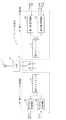
本発明に係るアンテナ共用器(7)においては、図1に示す如く、アンテナ(1)に対し、主スイッチング回路(3)を介して、従来方式のアンテナ共用回路(第1アンテナ共用回路(71))と、WCDMA送受信用のアンテナ共用回路(第2アンテナ共用回路(72))とが、切替え可能に接続されている。
【0017】
第1アンテナ共用回路(71)は、図3に示す従来方式のアンテナ共用器(70)と同じ構成であって、第1送受信回路(21)と第2送受信回路(22)を第1ダイプレクサ(2)によって切り替えるものである。GSMの受信時には、第1送受信回路(21)からGSM受信信号Rxgが出力され、GSMの送信時には、第1送受信回路(21)にGSM送信信号Txgが供給される。
又、DCSの受信時には、第2送受信回路(22)からDCS受信信号Rxdが出力され、PCSの受信時には、第2送受信回路(22)からPCS受信信号Rxpが出力される。更に、DCS又はPCSの送信時には、第2送受信回路(22)にDCS又はPCS送信信号Txdpが供給される。
【0018】
一方、第2アンテナ共用回路(72)は、WCDMA受信回路(81)とWCDMA送信回路(82)を第2ダイプレクサ(8)によって切り替えるものであり、WCDMAの受信時には、WCDMA受信回路(81)からWCDMA受信信号Rxwが出力される。又、WCDMAの送信時には、WCDMA送信回路(82)にWCDMA送信信号Txwが供給される。
【0019】
アンテナ(1)と主スイッチング回路(3)との間には、GSM、DCS又はPCSの送信信号の2倍以上の周波数帯域を抑圧することが可能な、例えば3GHzをカットオフ周波数とするローパスフィルター(9)が介在している。
【0020】
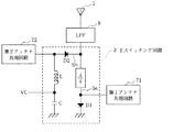
主スイッチング回路(3)は図2に示す構成を有している。即ち、ローパスフィルター(9)から第1アンテナ共用回路(71)へ繋がる分岐信号線Saには、λ/4ストリップラインが介在し、該λ/4ストリップラインと第1アンテナ共用回路(71)の連結点が、ダイオードD1を介して接地されている。又、ローパスフィルター(9)から第2アンテナ共用回路(72)へ繋がる分岐信号線Sbには、ダイオードD2が介在し、該ダイオードD2と第2アンテナ共用回路(72)の連結点は、インダクタンスL及びキャパシタンスCを介して接地されている。
【0021】
上記主スイッチング回路(3)においては、インダクタンスLとキャパシタンスCの連結点に対する制御信号VCをハイに設定すると、ダイオードD2がオンとなり、アンテナ(1)と第2アンテナ共用回路(72)が導通状態となる。また、同時にダイオードD1がオンとなり、第1アンテナ共用回路(71)は接地されると共に、λ/4ストリップラインによってアンテナ(1)と第1アンテナ共用回路(71)とが切断される。
これに対し、前記制御信号VCをローに設定すると、ダイオードD2がオフとなり、アンテナ(1)と第2アンテナ共用回路(72)が切断される。また、同時にダイオードD1がオフとなり、アンテナ(1)と第1アンテナ共用回路(71)とが導通状態となる。
上述の如く、制御信号VCのハイ/ローの切替えによって、第1アンテナ共用回路(71)又は第2アンテナ共用回路(72)を選択的にアンテナ(1)に接続することが出来る。
【0022】
尚、上記本発明のアンテナ共用器(7)は、積層モジュール構造を有するチップ部品として一体化されている。
【0023】
上記本発明のアンテナ共用器(7)においては、アンテナ(1)に第1アンテナ共用回路(71)を接続するべく主スイッチング回路(3)を切り替えたとき、該主スイッチング回路(3)を構成する2つのダイオードD1、D2がオフ(非導通状態)となるため、GSM送信信号Txg、DCS又はPCS送信信号Txdpの送信時に、これらの信号の整数倍(2倍、3倍・・・)の周波数を有するノイズが発生するが、該ノイズは、ローパスフィルター(9)を通過することによって十分に抑圧されることになる。
従って、該ノイズがアンテナ(1)から送信されることはない。
【0024】
又、上記本発明のアンテナ共用器(7)においては、主スイッチング回路(3)が2つのダイオードとLCの小型チップ部品の4点から構成されるため、例えば主スイッチング回路をGaAsスイッチICと大電流に対する保護回路とから構成した場合に比べて、部品点数が減少し、アンテナ共用器の小型化、低価格化が可能となる。
【図面の簡単な説明】
【図1】本発明に係るアンテナ共用器の構成を示すブロック図である。
【図2】主スイッチング回路の構成を示す回路図である。
【図3】従来のアンテナ共用器の構成を示すブロック図である。
【符号の説明】
(1) アンテナ
(7) アンテナ共用器
(9) ローパスフィルター
(3) 主スイッチング回路
(71) 第1アンテナ共用回路
(72) 第2アンテナ共用回路[0001]
TECHNICAL FIELD OF THE INVENTION
The present invention relates to an antenna duplexer provided in a mobile phone or the like.
[0002]
[Prior art]
FIG. 3 shows the configuration of an antenna duplexer (70) proposed by the applicant. According to the antenna duplexer (70), a DCS (Digital Cellular System) using a 1800 MHz band used in Europe is used. It is possible to transmit and receive triple band signals of PCS (Personal Communication Services) using 1900 MHz band used in North America and GSM (Global System For Mobile Communications) using 900 MHz band used in Europe and the like. (See Patent Document 1).
[0003]
As shown in FIG. 3, a first transmitting / receiving circuit (21) and a second transmitting / receiving circuit (22) are connected in parallel to the antenna (1) via a diplexer (2).
In the first transmitting / receiving circuit (21), a matching circuit (41) and a receiving SAW filter (51) are connected to one terminal of the switching circuit (31), and a GSM signal is received from the receiving SAW filter (51). Received signal Rxg is output. A transmission circuit (61) is connected to the other terminal of the switching circuit (31), and a GSM transmission signal Txg is supplied to the transmission circuit (61).
[0004]
In the second transmitting / receiving circuit (22), the first signal line S1 and the second signal line S2 are connected in parallel to one terminal of the switching circuit (32), and the DCS receiving line is connected to the first signal line S1. A matching circuit (42) and a SAW filter (52) intervene in series, and a matching circuit (43) for PCS reception and a SAW filter (53) intervene in series on the second signal line S2. Thus, the DCS reception signal Rxd is output from the first signal line S1, and the PCS reception signal Rxp is output from the second signal line S2.
A transmission circuit (62) is connected to the other terminal of the switching circuit (32), and a DCS transmission signal or a PCS transmission signal Txdp is supplied to the transmission circuit (62).
[0005]
The matching circuit (42) and the SAW filter (52) on the first signal line S1 are designed so that the DCS received signal Rx has an impedance of 50Ω and the PCS received signal Rx has a high impedance. On the other hand, the matching circuit (43) and the SAW filter (53) on the second signal line S2 are designed so that the DCS reception signal Rx has high impedance and the PCS reception signal Rx has 50Ω impedance.
[0006]
Therefore, at the time of DCS reception, the signal received by the antenna (1) passes through the diplexer (20) and the switching circuit (32), and further passes through the matching circuit (42) and the SAW filter (52) on the first signal line S1. As a result, the received signal Rxd of the DCS is extracted. At this time, since the matching circuit (43) and the SAW filter (53) on the second signal line S2 have high impedance in the band of the DCS reception signal Rxd, the isolation from the PCS reception signal Rxp is ensured. Is done.
[0007]
On the other hand, at the time of PCS reception, the signal received by the antenna (1) passes through the diplexer (20) and the switching circuit (32), and furthermore, the matching circuit (43) and the SAW filter (53) on the second signal line S2. ), The received signal Rxp of the PCS is extracted. At this time, since the matching circuit (42) and the SAW filter (52) on the first signal line S1 have high impedance in the band of the PCS reception signal Rxp, isolation from the DCS reception signal Rxd is ensured. Is done.
[0008]
[Patent Document 1]
Japanese Patent Application Laid-Open No. 2002-246809
[Problems to be solved by the invention]
By the way, as a third generation mobile communication system, WCDMA (wideband code division multiple access) that processes radio waves (1.9 to 2.2 GHz) having a wider frequency bandwidth than wireless communication based on the conventional CDMA (code division multiple access) system. A service of a wireless communication system called a system has been started.
Therefore, an antenna duplexer capable of performing transmission and reception in the WCDMA system in addition to transmission and reception in the DCS, PCS, and GSM is being developed.
[0010]
Such an antenna duplexer includes a conventional antenna shared circuit including a diplexer (20), a first transmission / reception circuit (21) and a second transmission / reception circuit (22) shown in FIG. 3, and an antenna shared circuit for WCDMA transmission / reception. Are connected to the antenna (1) via a switching circuit, and the switching circuit switches between the conventional antenna shared circuit and the WCDMA antenna shared circuit.
However, in this configuration, a noise having a frequency twice as high as the frequency of the DCS or PCS transmission signal Txdp obtained from the conventional antenna shared circuit due to the interposition of the switching circuit between the antenna and the antenna. And the noise is superimposed on the transmission signal and transmitted from the antenna (1).
[0011]
An object of the present invention is to reduce noise generated when a signal is transmitted by one of the antenna shared circuits in an antenna shared device configured to switch between two antenna shared circuits, for example, a conventional antenna shared circuit and a WCDMA transmission / reception antenna shared circuit. It is to suppress.
[0012]
[Means for solving the problem]
An antenna duplexer according to the present invention is an antenna duplexer for selectively receiving or transmitting a plurality of types of signals having different frequency bands with a common antenna (1). A first antenna shared circuit (71) for transmitting and receiving a first frequency band via a main switching circuit (3); and a second antenna for a second frequency band partially overlapping and adjacent to the first frequency band. A second antenna duplexer (72) for performing transmission and reception is switchably connected, and the first frequency band or the second frequency band is provided between the antenna (1) and the main switching circuit (3). A signal suppressing unit capable of suppressing a frequency band corresponding to twice the band is interposed.
[0013]
In a specific configuration, the signal suppressing unit is configured by a low-pass filter.
The main switching circuit (3) includes a pair of diodes connected to a signal line connected to the first antenna shared circuit (71) and a signal line connected to the second antenna shared device (72), respectively. It is constituted by a diode switch for switching between the first antenna shared circuit (71) and the second antenna shared device (72) by controlling the / non-conduction.
[0014]
In the antenna duplexer of the present invention, when the signal is transmitted from the first antenna shared circuit (71) due to the interposition of the main switching circuit (3), it is an integral multiple of the frequency band (first frequency band) of the signal. (2 times, 3 times,...) Noise is generated, and when transmitting a signal from the second antenna duplexer (72), an integer multiple (2 times, 2 times, Although noise having a frequency of three times... Is generated, the noise is sufficiently suppressed by passing through the signal suppressing means when transmitted from the antenna (1).
[0015]
【The invention's effect】
According to the antenna duplexer of the present invention, for example, in a configuration in which the conventional antenna shared circuit and the WCDMA transmission / reception antenna shared circuit are switched between two antenna shared circuits, noise generated when a signal is transmitted by one of the antenna shared circuits Can be sufficiently suppressed.
[0016]
BEST MODE FOR CARRYING OUT THE INVENTION
Hereinafter, embodiments of the present invention will be specifically described with reference to the drawings.
In the antenna duplexer (7) according to the present invention, as shown in FIG. 1, a conventional antenna shared circuit (first antenna shared circuit (71) is provided to the antenna (1) via the main switching circuit (3). )) And an antenna shared circuit for WCDMA transmission / reception (second antenna shared circuit (72)) are switchably connected.
[0017]
The first antenna shared circuit (71) has the same configuration as the conventional antenna shared device (70) shown in FIG. 3, and includes a first transmitting / receiving circuit (21) and a second transmitting / receiving circuit (22) in a first diplexer ( It is switched by 2). At the time of GSM reception, the GSM reception signal Rxg is output from the first transmission / reception circuit (21), and at the time of GSM transmission, the GSM transmission signal Txg is supplied to the first transmission / reception circuit (21).
Also, when receiving DCS, the DCS reception signal Rxd is output from the second transmission / reception circuit (22), and when receiving PCS, the PCS reception signal Rxp is output from the second transmission / reception circuit (22). Further, at the time of transmitting the DCS or PCS, the DCS or PCS transmission signal Txdp is supplied to the second transmission / reception circuit (22).
[0018]
On the other hand, the second antenna shared circuit (72) switches between the WCDMA receiving circuit (81) and the WCDMA transmitting circuit (82) by the second diplexer (8). WCDMA reception signal Rxw is output. Further, at the time of WCDMA transmission, a WCDMA transmission signal Txw is supplied to the WCDMA transmission circuit (82).
[0019]
Between the antenna (1) and the main switching circuit (3), a low-pass filter capable of suppressing a frequency band more than twice a GSM, DCS or PCS transmission signal, for example, having a cutoff frequency of 3 GHz. (9) is interposed.
[0020]
The main switching circuit (3) has the configuration shown in FIG. That is, a λ / 4 strip line is interposed in the branch signal line Sa connected from the low-pass filter (9) to the first antenna shared circuit (71), and the λ / 4 strip line and the first antenna shared circuit (71) are interposed. The connection point is grounded via a diode D1. A diode D2 is interposed in the branch signal line Sb connecting the low-pass filter (9) to the second antenna shared circuit (72), and a connection point between the diode D2 and the second antenna shared circuit (72) is an inductance L. And a ground via a capacitance C.
[0021]
In the main switching circuit (3), when the control signal VC for the connection point between the inductance L and the capacitance C is set high, the diode D2 is turned on, and the antenna (1) and the second antenna shared circuit (72) are in a conductive state. It becomes. At the same time, the diode D1 is turned on, the first antenna shared circuit (71) is grounded, and the antenna (1) and the first antenna shared circuit (71) are disconnected by the λ / 4 strip line.
On the other hand, when the control signal VC is set to low, the diode D2 is turned off, and the antenna (1) and the second antenna shared circuit (72) are disconnected. At the same time, the diode D1 is turned off, and the antenna (1) and the first antenna shared circuit (71) are brought into conduction.
As described above, the first shared antenna circuit (71) or the second shared antenna circuit (72) can be selectively connected to the antenna (1) by switching the control signal VC between high and low.
[0022]
The antenna duplexer (7) of the present invention is integrated as a chip component having a laminated module structure.
[0023]
In the antenna duplexer (7) of the present invention, when the main switching circuit (3) is switched to connect the first antenna shared circuit (71) to the antenna (1), the main switching circuit (3) is configured. Since the two diodes D1 and D2 are turned off (non-conducting state), when the GSM transmission signal Txg, DCS or PCS transmission signal Txdp is transmitted, an integer multiple (2 times, 3 times,. Although noise having a frequency is generated, the noise is sufficiently suppressed by passing through the low-pass filter (9).
Therefore, the noise is not transmitted from the antenna (1).
[0024]
Further, in the antenna duplexer (7) of the present invention, the main switching circuit (3) is composed of two diodes and four small chip components of LC. The number of components is reduced as compared with the case where the current protection circuit is used, and the antenna duplexer can be reduced in size and cost.
[Brief description of the drawings]
FIG. 1 is a block diagram illustrating a configuration of an antenna duplexer according to the present invention.
FIG. 2 is a circuit diagram showing a configuration of a main switching circuit.
FIG. 3 is a block diagram showing a configuration of a conventional antenna duplexer.
[Explanation of symbols]
(1) Antenna (7) Antenna duplexer (9) Low-pass filter (3) Main switching circuit (71) First antenna shared circuit (72) Second antenna shared circuit