JP2004191244A - Spectrograph and correction method - Google Patents
Spectrograph and correction method Download PDFInfo
- Publication number
- JP2004191244A JP2004191244A JP2002360996A JP2002360996A JP2004191244A JP 2004191244 A JP2004191244 A JP 2004191244A JP 2002360996 A JP2002360996 A JP 2002360996A JP 2002360996 A JP2002360996 A JP 2002360996A JP 2004191244 A JP2004191244 A JP 2004191244A
- Authority
- JP
- Japan
- Prior art keywords
- light
- correction
- wavelength
- light receiving
- intensity distribution
- Prior art date
- Legal status (The legal status is an assumption and is not a legal conclusion. Google has not performed a legal analysis and makes no representation as to the accuracy of the status listed.)
- Pending
Links
Images


Landscapes
- Spectrometry And Color Measurement (AREA)
Abstract
Description
【0001】
【発明の属する技術分野】
本発明は、可視光、赤外線又は紫外線の測定光の分光強度分布を測定する分光装置に関し、特に、波長精度を略初期状態に戻す補正機能を備える分光装置に関する。
【0002】
【従来の技術】
従来、分光装置の分光手段として、測定光を波長毎に分散し、この分散された各波長の光を受光する光電変換素子アレイにより分散光を同時測定するポリクロメータが知られている。このポリクロメータは、可動部が無く、回折格子とレンズや凹面鏡等の結像光学系とを組み合わせたものや、この組み合わせたものと同一機能を果たす凹面回折格子により、測定光を波長毎に分散すると共に、分散された光の像を光電変換素子アレイ上に結像させて、各波長の強度を同時測定するように構成されている。
【0003】
このような分光手段の波長精度は、結像光学系の光学素子、分光素子及び受光素子等の各光学要素における相対位置変化に敏感であるため、高精度を実現及び維持するためには、使用を始めてからも補正を行う必要がある。分光手段の補正を行うためには、一般に、安定した波長基準が必要である。安定した波長基準は、例えば、レーザ光源や輝線光源フィルタ等が用いられるが、この光源装置は、コストが高く、フィルタは、精度を維持するために周囲温度を一定に保持する必要がある等の理由から、分光装置に組み込むことが難しく、また、ユーザ自身が取り扱うことも困難である。そのため、ユーザは、通常年に1回程度、分光装置をメーカに返送してメーカに補正を依頼することが多い。
【0004】
一方、上述のように、分光手段の波長精度が各光学要素の相対位置の変化に敏感であることから、これら光学要素を支持する支持部材に経時変化や温度変化に対して安定な金属材料が用いられている。
【0005】
なお、分光手段の校正に関し、例えば、特許文献1がある。この特許文献1には、被校正ポリクロメータと基準ポリクロメータとを同一構成でそれぞれ用意し、被校正ポリクロメータから得たデータと、基準ポリクロメータから得たデータと、既知として予め記憶されている基準ポリクロメータの分光感度特性とに基づいて校正を行う分光装置が開示されている。
【0006】
【特許文献1】
特開平12−205955号公報
【0007】
【発明が解決しようとする課題】
ところで、従来の補正方法では、通常年に1回程度の補正であるため、補正後から次の補正までの間における波長精度が保証されないという問題がある。そして、メーカに補正を依頼しなければならないため、補正を依頼する間は分光装置を利用することができない、返送等の依頼に手間がかかる、依頼の費用が掛かる等の問題も生じる。
【0008】
一方、従来の補正方法では、上述のように支持部材に安定な部材を採用しなければならず、安価なABS、ポリカーボネート等の汎用プラスチック材料を用いることが困難であることから、低廉化や軽量化の障害となっていた。
【0009】
そこで、本発明は、上記事情に鑑みて為された発明であり、各光学要素の相対位置の変化により波長シフトが生じたとしても、測定時に補正することにより、初期の波長精度を維持することができる分光装置及び補正方法を提供することを目的とする。
【0010】
【課題を解決するための手段】
上述の目的を達成するために、請求項1に係る分光装置は、補正用の光を発光する光源と、入射される光を波長に応じて分散する分散手段と、前記分散手段で分散した光を受光し、受光した各波長成分の光強度に応じた電気信号を出力する光電変換素子が配列されてなる受光手段と、測定光が入射され前記分散手段を介して前記受光手段上に波長分散像を結像する第1入射開口と、前記補正用の光が入射され前記分散手段を介して前記受光手段上に0次反射光による像を結像する第2入射開口と、測定光の波長と該波長に対応する光電変換素子に割り当てられた画素番号との対応関係を示す波長画素番号対応情報を予め記憶する波長画素番号対応情報記憶手段と、前記受光手段の出力に基づく前記補正用の光の強度分布である基準プロファイルを予め記憶する基準プロファイル記憶手段と、補正量を求める場合には前記受光手段の出力に基づく前記補正用の光の強度分布である補正時時プロファイルと前記基準プロファイルとを比較することによって前記補正時プロファイルと前記基準プロファイルとにおける前記受光手段上の結像位置の差を前記補正量として求め前記補正量を補正量記憶手段に記憶すると共に、測定光の分光強度分布を求める場合には前記受光手段の出力と前記波長画素番号対応情報と前記補正量とに基づいて補正し前記測定光の分光強度分布を求める演算処理手段とを備える。
【0011】
そして、請求項5では、補正用の光を発光する光源と、入射される光を波長に応じて分散する分散手段と、前記分散手段で分散した光を受光し受光した各波長成分の光強度に応じた電気信号を出力する光電変換素子が配列されてなる受光手段と、測定光が入射され前記分散手段を介して前記受光手段上に波長分散像を結像する第1入射開口と、前記補正用の光が入射され前記分散手段を介して前記受光手段上に0次反射光による像を結像する第2入射開口と、情報を記憶する記憶手段と、測定光の分光強度分布を求める演算処理手段とを備える分光装置の波長シフトを補正する補正方法において、前記演算処理手段は、前記受光手段の出力に基づく前記補正用の光の強度分布である基準プロファイルを予め前記記憶手段に記憶するステップと、補正量を求める場合には前記受光手段の出力に基づく前記補正用の光の強度分布である補正時プロファイルと前記基準プロファイルとを比較することによって前記補正時プロファイルと前記基準プロファイルとの前記受光手段上の結像位置の差を前記補正量として求めるステップと、求めた前記補正量を前記記憶手段に記憶するステップと、測定光の分光強度分布を求める場合には前記受光手段の出力を前記補正量で補正することによって前記測定光の分光強度分布を求めるステップとを実行する。
【0012】
このような分光装置及び分光装置の補正方法では、補正用の光による分光強度分布である基準プロイファイルを基準プロファイル記憶手段や記憶手段に製造時や出荷時等に予め記憶しておくので、補正量を求める場合に、補正時に求めた補正用の光による強度分布である補正時プロイファイルと基準プロファイルとを比較することができ、この比較から補正量を求めることができる。そのため、測定光の強度分布をこの補正量で補正することができるから、製造時や出荷時等の基準プロファイルを記憶した時点における波長精度で測定光の分光強度分布を測定することができる。
【0013】
このため、安定な基準波長の光を発光するレーザ光源や輝線光源等を組み込む必要が無く、また、フィルタの透過特性を安定にするために周囲温度を一定に保つ必要がないので、分光装置の大型化やコストアップを抑制することができる。さらに、光源、第1入射開口、第2入射開口、分散手段及び受光手段等の光学要素を支持する支持部材に必ずしも経時的に及び熱的に安定な材料を用いる必要がないので、支持部材に安価な又は軽量な材料を用いることができる。
【0014】
また、第1入射開口と第2入射開口の相対位置は、略一定に保たれるべく構成される。請求項2では、請求項1に記載の分光装置において、前記第1入射開口及び前記第2入射開口は、経時的に前記第1入射開口と前記第2入射開口との相対位置が略一定である材料の板に形成される。このような分光装置では、経時的に精度よく補正することができる。
【0015】
そして、請求項3では、請求項1又は請求項2に記載の分光装置において、前記第1入射開口及び前記第2入射開口は、温度変化に対して前記第1入射開口と前記第2入射開口との相対位置が略一定である材料の板に形成される。このような分光装置では、温度変化があっても精度よく補正することができる。
【0016】
さらに、請求項4では、請求項1乃至請求項3の何れか1項に記載の分光装置において、前記補正用の光が点灯されている間に測定光を遮光する遮光手段をさらに備える。
【0017】
このような分光装置では、遮光手段を備えるので、補正用の光による基準プロファイルや補正時プロファイルを得る場合に測定光を確実に遮光することができ、測定光がこれらプロファイルに与える影響を考慮する必要がなくなる。
【0018】
【発明の実施の形態】
以下、本発明に係る実施形態を図面に基づいて説明する。なお、各図において同一の構成については、同一の符号を付し、その説明を省略する。まず、本実施形態の構成について説明する。
(実施形態の構成)
図1は、本実施形態における分光輝度計の要部の構成を示す図である。
【0019】
図1において、分光輝度計200は、受光光学系11、入射開口板12、結像光学系13、回折格子14、受光センサアレイ15、光源16、駆動部17、信号処理部18、アナログ/ディジタル変換部(A/D変換部)19、演算処理部20及び記憶部21を備えて構成される。
【0020】
測定光10は、受光光学系11によって収束され、第1入射開口12aに入射する。第1入射開口12aは、第2入射開口12bと共に入射開口板12に設けられる。入射開口板12は、波長精度を高精度で維持する観点から、通常の使用年数における経時変化に対し、又は、通常の使用環境における温度変化に対し第1入射開口12aと第2入射開口12bとの相対位置が略一定である材料、例えば、経時的に及び熱的に安定性の高い材料、より具体的には、例えば、このような金属材料(例えば、熱膨張係数の小さいSUS430やインバー鋼やチタン等)が好ましい。
【0021】
第1入射開口12aを通過した光束10aは、結像光学系13によって平行光束となって、回折格子14に入射する。回折格子14に入射した平行光束は、波長毎に波長に応じて異なる方向に分散反射し、再び結像光学系13に入射する。そして、結像光学系13は、受光センサアレイ15上に第1入射開口12aの波長分散像10bを結像する。受光センサアレイ15は、光電変換素子が等間隔に配列されており、各光電変換素子は、受光した光強度に応じた電流を生成する。
【0022】
受光センサアレイ15の出力は、信号処理部18に入力され、電流/電圧変換等の信号処理を経て、A/D変換部19に入力される。A/D変換部19は、信号処理部18でそれぞれ処理された受光センサアレイ15における各光電変換素子の出力をアナログ信号からディジタル信号に変換し、ディジタル信号に変換された各光電変換素子の出力を演算処理部20に出力する。演算処理部20は、入力された各光電変換素子の出力を後述のように処理する。
【0023】
一方、光源16は、入射開口板12における第2入射開口12bの受光光学系11側に配置される。光源16は、駆動部17によって駆動され、補正用の光(補正光)を発光する。発光タイミング及び発光時間は、駆動部17を介して演算処理部20によって制御される。第2入射開口12bは、第1入射開口12aから一定距離離れた位置で入射開口板12に設けられる。この第2入射開口12bの位置は、第2入射開口12bを通過した補正光の光束6aが結像光学系13によって平行光束となり、回折格子14による0次反射光が結像光学系13によって第2入射開口12bの像を受光センサアレイ15上に結像するような位置である。そして、補正光の波長は、回折格子14による0次反射光が充分に得られるように選択される。例えば、回折格子14が可視域用の場合にはブレーズ波長が短波長になるようにブレーズされたものが多いため、光源16は、赤外或いは赤の発光ダイオード(LED)とすることで十分な0次反射光が得られる。
【0024】
また、記憶部21は、後述の波長画素番号対応情報を記憶する波長画素番号対応情報記憶部211、基準プロファイルを記憶する基準プロファイル記憶部212、補正量を記憶する補正量記憶部213を備え、さらに、演算処理部20が実行するプログラムやプログラム実行中のデータ等を記憶し、例えば、ROMやRAMで構成される。
【0025】
そして、測定光を遮光する場合には、受光光学系11の入射側に着脱可能な遮光キャップ8を装着する。遮光キャップ8は、例えば、光源16より補正用の光が点灯されている間に測定光を遮光するために使用される。
【0026】
次に、本実施形態の動作について説明する。
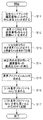
(製造工程における波長校正の動作)
図2は、製造工程における波長校正の動作を示すフローチャートである。図3は、受光センサアレイにおける各光電変換素子の波長に対する受光感度を示す図である。図3の横軸はnm単位で示す波長であり、その縦軸は相対感度である。図4は、画素番号nと相対強度Anとの関係を示す図である。図4の横軸は画素番号nであり、その縦軸は相対強度である。図5は、シフト基準プロファイルの一例を示す図である。図5の横軸は画素番号変数xであり、その縦軸は相対強度である。
【0027】
図2において、まず、演算処理部20は、周知の方法で、図3に示すように、画素番号nにおける光電変換素子の中心波長λcnをそれぞれ求める(S11)。画素番号nは、受光センサアレイ15における各光電変換素子に対し順に割り振った番号であり、n=1、2、3、・・・、Nである。
【0028】
次に、演算処理部20は、処理S11の測定結果を用いて任意の波長λを中心波長とする画素番号変数xを与える関数fx(λ)を求める(S12)。図3から分かるように、隣接する各画素の中心波長は、略等間隔であるが、厳密には等間隔ではなく、画素番号と中心波長との関係を表す関数fx(λ)は、一次式にならない。本実施形態では、関数fx(λ)として計算の容易性等の観点から例えば3次や4次、ここでは4次の多項式を用いることができる。
fx(λ)=D0+D1・λ+D2・λ2+D3・λ3+D4・λ4 ・・・(1)
ここで、この式1の各次数に対する係数D0、D1、D2、D3及びD4は、画素番号nに対応する中心波長λcnのデータを用いて最小自乗法によって求める。
【0029】
次に、演算処理部20は、式1を用いて、分光強度分布の名目波長Λmに対応する画素番号xm=fx(Λm)を求めて、名目波長とこの波長を中心波長とする画素番号との対応関係を示す波長画素番号対応情報として記憶部21の波長画素番号対応情報記憶部211に記憶する(S13)。ここで、mは、1、2、3、・・・、Mの正数であり、例えば、受光センサアレイ15が10nmピッチで360nmから740nmまでの波長域を受光可能とすればM=39となる。
【0030】
次に、遮光キャップ8を受光光学系11の入射側に装着することによって受光光学系11に入射する光を遮断する。なお、第1入射開口12aに入射される光が遮断されればよいので、遮光キャップ8に限らず、受光光学系11の入射側から第1入射開口12aまでの間に遮光板等を用いて遮光してもよい。その後、演算処理部20は、駆動部17を介して光源16を点灯することによって補正光を発光させ、回折格子の0次光による第2入射開口12bの像を受光センサアレイ15上に生成させる。そして、演算処理部20は、受光センサアレイ15から信号処理部18及びA/D変換部19を介して、例えば図4に示すような画素番号nの光電変換素子の出力A(n)を得る(S14)。
【0031】
次に、演算処理部20は、さらにA(n)を補間して画素番号変数xの関数としての基準プロファイルAs(x)を求め(S15)、さらに、図5に示すように、結像位置を受光センサアレイ15上で少しずつシフト(移動)させたシフト基準プロファイルAk(x’)を求める(S16)。ここで、シフト基準プロファイルAk(x’)は、単位変化量をdxとし、変化量をk・dxとすれば、処理S15で求めた基準プロファイルAs(x)の画素番号変数xをx+k・dx(=x’)に座標変換することによって求めることができる。即ち、式2のようになる。
Ak(x’)=As(x+k・dx) ・・・ (2)
ここで、単位変化量dxは、例えば、波長変化(例えば0.1nm)に相当する画素番号の変化とし、変化量k・dxは、例えば、k=−10、−9、・・・、9、10として−1nmから+1nmに相当する画素番号の変化とする。
【0032】
そして、演算処理部20は、求めたシフト基準プロファイルAk(x’)を画素番号の変化量k・dxと対応付けて記憶部21の基準プロファイル記憶部212に記憶する(S17)。
【0033】
以上のように動作することによって、分光輝度計200は、補正に必要な基礎データとなるシフト基準プロファイルAk(x’)データと対応する画素番号の変化量k・dxデータを記憶部21に記憶することができる。
【0034】
次に、測定時における分光輝度計200の動作について説明する。
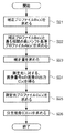
(測定時の動作)
図6は、測定する場合の動作を示すフローチャートである。
【0035】
図6において、まず、基準プロファイルを求めた場合と同様に、遮光キャップ8を受光光学系11に装着することによって受光光学系11に入射する光を遮断する。その後、演算処理部20は、駆動部17を介して光源16を点灯することによって補正光を発光させ、回折格子の0次光による第2入射開口12bの像を受光センサアレイ15上に生成させる。そして、演算処理部20は、受光センサアレイ15から信号処理部18及びA/D変換部19を介して、画素番号nの光電変換素子の出力B(n)を得て、基準プロファイルAs(x)と同様に補間を行って補正時プロファイルBs(x)を求める(S21)。
【0036】
次に、演算処理部20は、補正時プロファイルBs(x)と、記憶部21に格納されている各シフト基準プロファイルAk(x’)との相関Crkを順次にそれぞれ求めることによって、最も相関の高いシフト基準プロファイルAk(x’)を求める(S22)。
【0037】
ここで、補正時プロファイルBs(x)とシフト基準プロファイルAk(x’)との相関Crkは、式3を用いて算出される。
Crk={r(Bs(x)、Ak(x’))}2/{r(Bs(x)、Bs(x))・r(Ak(x’)、Ak(x’))}
r(P(x)、Q(x))=∫P(x)・Q(x)dx・・・ (3)
そして、演算処理部20は、最も相関の高いシフト基準プロファイルAk(x’)に対応する画素番号の変化量k・dx(補正量)を求め、基準プロファイルAs(x)と補正時プロファイルBs(x)との結像位置変化とする。演算処理部20は、変化量k・dx(補正量)を記憶部21の補正量記憶部213に記憶する(S23)。
【0038】
本実施形態では、この画素番号の変化量k・dxで表した基準プロファイルAs(x)と補正時プロファイルBs(x)との結像位置変化が受光センサアレイ15における全ての光電変換素子上に生じていると見做し、この変化量k・dxによって分光強度分布の波長シフトを補正する。即ち、式4に示すように、記憶部21に格納されている名目波長Λmに対応する画素番号xmを、求めた画素番号の変化量k・dxで補正する。
x’m=xm+k・dx ・・・ (4)
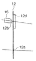
なお、補正時プロファイルBs(x)とシフト基準プロファイルAk(x’)とを比較することによって結像位置の差を光電変換素子のピッチ(繰り返しの間隔)より小さい分解能で推定するためには、第2入射開口12bの像は、受光センサアレイ15における複数の光電変換素子上に強度分布、特に単純な曲線の強度分布を持つ必要がある。上述の実施形態では、結像光学系13の収差を利用したが、図7に示すように、第2入射開口12bの射出側に拡散板12dを設けることによって積極的に単純な曲線の強度分布を得るようにしてもよい。
【0039】
その後、演算処理部20は、駆動部17を介して光源16を消灯する。また、遮光キャップ8を除いて測定光が受光光学系11を介して第1入射開口に入射可能となるように設定する。そして、測定光を受光光学系11に入射させ、演算処理部20は、受光センサアレイ15から信号処理部18及びA/D変換部19を介して、測定光に対する画素番号nの光電変換素子の出力C(n)を得て(S24)、基準プロファイルAs(x)と同様に補間を行って測定光プロファイルCs(x)を求める(S25)。
【0040】
次に、演算処理部20は、求めた測定光プロファイルCs(x)のxに式4のx’mを代入することによって、波長シフト補正された名目波長Λmで分光強度C(x’m)を求める(S26)。
【0041】
なお、続けて測定する場合には、改めて処理21から開始してもよいが、処理S24から開始してもよい。測定時の補正は、絶えず初期の波長精度を維持する観点から測定ごとに自動的に行うように構成してもよく、演算処理部20の負担の軽減や測定時間を短縮する観点から電源を投入した後に自動的に一度だけ行うように構成してもよい。また、補正開始を指示するスイッチを設け、ユーザの所望によりこのスイッチをオンすることによって補正を行うように構成してもよい。
【0042】
本実施形態に係る分光輝度計200は、シフト基準プロファイルAk(x’)を記憶部21に備え、これを用いて測定時における補正量を求めることができるので、分光手段の光学要素の相対位置が経時的、熱的に変化することによって分光手段に波長シフトが生じたとしても、初期の波長校正時における波長精度で測定することができ、また、ユーザ側で補正することができる。
【0043】
なお、上述の実施形態では、画素番号の変化量k・dxで表した基準プロファイルAs(x)と補正時プロファイルBs(x)との結像位置変化で受光センサアレイ15全域での結像位置の変化を補正しているが、さらに精度を上げる観点から、結像位置変化を結像位置の関数としてもよい。例えば、変化量(補正量)k・dxのdxを結像位置xの関数としてもよい。
【0044】
そして、入射開口板12、結像光学系13、回折格子14及び受光センサアレイ15等の各光学要素における経時的、熱的な相対位置変化は、さまざまに起こり得る。ここで、受光センサアレイ15の波長分散方向(図1におけるA方向)における位置変化によって生じる結像位置変化は、結像位置に依らず一定である。一方、入射開口板12の両入射開口配設方向(図1におけるB方向)における位置変化や結像光学系13の垂直方向(図1におけるC方向)における位置変化、回折格子14の回転(図1におけるD方向、図面の紙面に対して垂直な方向を軸とする回転)によって生じる結像位置変化は、回折格子14からの射出角の変化を経て生じるため、その量は、結像位置に依存する。例えば、第2入射開口12bの0次光による像の結像位置x0での結像位置変化がdx0の場合の、任意の結像位置xにおける結像位置変化dx(x)は、幾何学的な考察から得ることができ、小型化のため、第1入射開口12aと第2入射開口12bとの間隔を短くすると、図1から分かるように、第2入射開口12bの0次光による像は、受光センサアレイ15の短波長領域に結像し、これから離れた長波長域での結像位置変化をより正確に演算することができる。
【0045】
さらに、受光センサアレイ15の波長分散方向(図1のA方向)における位置変化によって生じる結像位置変化(受光センサアレイ15上の結像位置に依らず均一に変化する)を取り除く観点から、図8に示すように、入射開口板12に受光センサアレイ15も取り付けるようにしてもよい。即ち、第1入射開口12a、第2入射開口12b及び受光センサアレイ15を1枚の入射開口板12’に設ける。この場合では、起こり得る結像位置変化は、明確に回折格子14からの射出角の変化を経て生じるので、前述の幾何学的な考察による各結像位置での補正量の精度を高めることができる。
【0046】
図9は、回折格子からの射出各の変化において、0次反射方向の変化と1次回折方向の変化との関係を示す図である。図9に示すように、回折格子Gにおいて、0次反射方向がR0からR0’へd0だけ変化したときに、1次回折方向がR1からR1’へd1だけ変化する。ここで、回折格子Gの格子定数を600本/mm、波長を550nm、d0を0.0036度(1nmの波長シフトに相当する。)とすると、d1とd0との差は6パーセント程度であり、1次回折方向の変化を0次反射方向の変化としても大きな誤差とはならないことが分かる。
【0047】
そして、上述の実施形態において、警告を提示する警告手段と補正量の許容範囲の限界値である閾値を記憶する閾値記憶手段とを分光輝度計200にさらに備えさせ、演算処理部20は、さらに、画素番号の変化量k・dx(補正量)が所定の閾値以上となった場合には、許容誤差以上の波長シフトが生じたことをユーザに警告するように構成してもよい。このように構成することによって、ユーザは、警告されるまで所定範囲内の精度で測定されるから、安心して測定を続けることができ、警告を受けた場合には、補正の時機が来たことを認識することができる。ここで、警告手段は、LED等のランプやブザー等の警告音を発生させる警告音発生手段やLCD等に警告メッセージを表示する警告表示手段等である。
【0048】
以上、本明細書に開示された主な発明を以下にまとめる。
(付記1)補正用の光を発光する光源と、入射される光を波長に応じて分散する分散手段と、前記分散手段で分散した光を受光し、受光した各波長成分の光強度に応じた電気信号を出力する光電変換素子が配列されてなる受光手段と、測定光が入射され前記分散手段を介して前記受光手段上に波長分散像を結像する第1入射開口と、前記補正用の光が入射され前記分散手段を介して前記受光手段上に0次反射光による像を結像する第2入射開口と、測定光の波長と該波長に対応する光電変換素子に割り当てられた画素番号との対応関係を示す波長画素番号対応情報を予め記憶する波長画素番号対応情報記憶手段と、前記受光手段の出力に基づく前記補正用の光の強度分布である基準プロファイルを予め記憶する基準プロファイル記憶手段と、補正量を求める場合には前記受光手段の出力に基づく前記補正用の光の強度分布である補正時プロファイルと前記基準プロファイルとを比較することによって前記補正時プロファイルと前記基準プロファイルとにおける前記受光手段上の結像位置の差を前記補正量として求め前記補正量を補正量記憶手段に記憶すると共に、測定光の分光強度分布を求める場合には前記受光手段の出力と前記波長画素番号対応情報と前記補正量とに基づいて補正し前記測定光の分光強度分布を求める演算処理手段とを備えることを特徴とする分光装置。
(付記2)前記第1入射開口及び前記第2入射開口は、経時的に前記第1入射開口と前記第2入射開口との相対位置が略一定である材料の板に形成されることを特徴とする付記1に記載の分光装置。
(付記3)前記第1入射開口及び前記第2入射開口は、温度変化に対して前記第1入射開口と前記第2入射開口との相対位置が略一定である材料の板に形成されることを特徴とする付記1又は付記2に記載の分光装置。
(付記4)前記補正用の光が点灯中に測定光を遮光する遮光手段をさらに備えることを特徴とする付記1乃至付記3の何れかに記載の分光装置。
(付記5)前記基準プロファイル記憶手段は、前記基準プロファイルを所定の画素番号間隔でシフトしたシフト基準プロファイルを記憶し、
前記演算処理手段は、前記補正時プロファイルとシフト基準プロファイルとの相関を求めることによって前記補正量を求めることを特徴とする付記1乃至付記4に記載の分光装置。
(付記6)前記演算処理手段は、前記補正量を電源投入時に求めて補正量記憶手段に記憶することを特徴とする付記1乃至付記5に記載の分光装置。
(付記7)前記演算処理手段は、前記補正量をユーザの指示があった場合に求めて補正量記憶手段に記憶することを特徴とする付記1乃至付記5に記載の分光装置。
(付記8)補正用の光を発光する光源と、入射される光を波長に応じて分散する分散手段と、前記分散手段で分散した光を受光し、受光した各波長成分の光強度に応じた電気信号を出力する光電変換素子が配列されてなる受光手段と、測定光が入射され前記分散手段を介して前記受光手段上に波長分散像を結像する第1入射開口と、前記補正用の光が入射され前記分散手段を介して前記受光手段上に0次反射光による像を結像する第2入射開口と、前記受光手段の出力に基づく前記補正用の光の強度分布である基準プロファイル(基準プロファイルをもとに求められたシフト基準プロファイルを含む)を予め記憶する基準プロファイル記憶手段と、警告を提示する警告手段と、補正量の許容範囲の限界値である閾値を記憶する閾値記憶手段と、前記受光手段の出力に基づく前記補正用の光の強度分布である補正時プロファイルと前記基準プロファイルとを比較することによって前記補正時プロファイルと前記基準プロファイルとの前記受光手段上の結像位置の差を補正量として求めると共に、求めた前記補正量が前記閾値以上である場合には前記警告手段で警告を提示する演算処理手段とを備えることを特徴とする分光装置。
(付記9)補正用の光を発光する光源と、入射される光を波長に応じて分散する分散手段と、前記分散手段で分散した光を受光し受光した各波長成分の光強度に応じた電気信号を出力する光電変換素子が配列されてなる受光手段と、測定光が入射され前記分散手段を介して前記受光手段上に波長分散像を結像する第1入射開口と、前記補正用の光が入射され前記分散手段を介して前記受光手段上に0次反射光による像を結像する第2入射開口と、情報を記憶する記憶手段と、測定光の分光強度分布を求める演算処理手段とを備える分光装置の波長シフトを補正する補正方法において、前記演算処理手段は、前記受光手段の出力に基づく前記補正用の光の強度分布である基準プロファイル(基準プロファイルをもとに求められるシフト基準プロファイルを含む)を予め前記記憶手段に記憶するステップと、補正量を求める場合には前記受光手段の出力に基づく前記補正用の光の強度分布である補正時プロファイルと前記基準プロファイルとを比較することによって前記補正時プロファイルと前記基準プロファイルとの前記受光手段上の結像位置の差を前記補正量として求めるステップと、求めた前記補正量を前記記憶手段に記憶するステップと、測定光の分光強度分布を求める場合には前記受光手段の出力を前記補正量で補正することによって前記測定光の分光強度分布を求めるステップとを実行することを特徴とする補正方法
【0049】
【発明の効果】
以上のように、請求項1に係る分光装置及び請求項5に係る分光装置の補正方法は、基準プロイファイルを基準プロファイル記憶手段や記憶手段に製造時や出荷時等に予め記憶しておくので、補正量を求める場合に、補正時に求めた補正時プロイファイルと基準プロファイルとを比較することができ、この比較から補正量を求めることができる。そのため、測定光の分光強度分布をこの補正量で補正することができるから、製造時や出荷時等の基準プロファイルを記憶した時点における波長精度で測定光の分光強度分布を測定することができる。そして、分光装置自体に補正手段が組み込まれているので、日常的に補正することが可能であり、メーカに補正を依頼する必要が無いから、いつでも分光装置を利用することができ、返送等の依頼の手間がかからず、依頼の費用も掛からない。さらに、光源、第1入射開口、第2入射開口、分散手段及び結像手段等の光学要素を支持する支持部材に必ずしも経時的に及び熱的に安定な材料を用いる必要がないので、支持部材に安価な又は軽量な材料を用いることができる。
【0050】
また、第1入射開口と第2入射開口の相対位置は、略一定に保たれるべく構成される。請求項2に係る分光装置は、請求項1の効果に加えて、第1及び第2入射開口を形成する板に経時的に両入射開口の相対位置が略一定である材料を用いるので、経時的に精度よく補正することができる。
【0051】
そして、請求項3に係る分光装置は、請求項1及び請求項2の効果に加えて、第1及び第2入射開口を形成する板に温度変化に対して両入射開口の相対位置が略一定である材料を用いるので、温度変化に対して精度よく補正することができる。
【0052】
さらに、請求項4に係る分光装置は、請求項1乃至請求項3の効果に加えて、遮光手段を備えるので、補正用の光による基準プロファイルや補正時プロファイルを得る場合に測定光を確実に遮光することができ、測定光がこれら分光プロファイルに与える影響を考慮する必要がなくなる。
【図面の簡単な説明】
【図1】本実施形態における分光輝度計の要部の構成を示す図である。
【図2】製造工程における波長校正の動作を示すフローチャートである。
【図3】受光センサアレイにおける各光電変換素子の波長に対する受光感度を示す図である。
【図4】画素番号nと相対強度Anとの関係を示す図である。
【図5】シフト基準プロファイルの一例を示す図である。
【図6】測定する場合の動作を示すフローチャートである。
【図7】拡散板を用いる場合における、分光輝度計の拡散板周辺の構成を示す図である。
【図8】本実施形態の変形形態における分光輝度計の要部の構成を示す図である。
【図9】回折格子からの射出各の変化において、0次反射方向の変化と1次回折方向の変化との関係を示す図である。
【符号の説明】
8 遮光キャップ、12 入射開口板、12a 第1入射開口、12b、第2入射開口、14 回折格子、15 受光センサアレイ、16 光源、20 演算処理部、21 記憶部、200 分光輝度計、211 波長画素番号対応情報記憶部、212 基準プロファイル記憶部、213 補正量記憶部[0001]
TECHNICAL FIELD OF THE INVENTION
The present invention relates to a spectrometer for measuring a spectral intensity distribution of measurement light of visible light, infrared light or ultraviolet light, and more particularly to a spectrometer having a correction function for returning wavelength accuracy to a substantially initial state.
[0002]
[Prior art]
2. Description of the Related Art Conventionally, as a spectroscopic unit of a spectroscopic device, a polychromator that disperses measurement light for each wavelength and simultaneously measures the dispersed light by a photoelectric conversion element array that receives the dispersed light of each wavelength is known. This polychromator has no movable parts and combines a diffraction grating with an imaging optical system such as a lens or a concave mirror, or a concave diffraction grating that performs the same function as this combination, and disperses the measurement light for each wavelength. At the same time, the image of the dispersed light is formed on the photoelectric conversion element array, and the intensity of each wavelength is measured simultaneously.
[0003]
The wavelength accuracy of such a spectral unit is sensitive to changes in the relative position of each optical element such as the optical element, the spectral element, and the light receiving element of the imaging optical system. It is necessary to perform the correction even after starting. In general, a stable wavelength reference is required to correct the spectral means. As a stable wavelength reference, for example, a laser light source or an emission line light source filter is used. However, this light source device is expensive, and the filter needs to maintain a constant ambient temperature in order to maintain accuracy. For this reason, it is difficult to incorporate it into the spectroscopic device, and it is also difficult for the user to handle it. For this reason, the user often returns the spectroscopic device to the manufacturer about once a year and requests the manufacturer to perform correction.
[0004]
On the other hand, as described above, since the wavelength accuracy of the spectroscopic means is sensitive to changes in the relative positions of the optical elements, a metal material that is stable against aging and temperature changes is provided on a support member that supports these optical elements. Used.
[0005]
Note that there is, for example,
[0006]
[Patent Document 1]
JP-A-12-205955
[0007]
[Problems to be solved by the invention]
By the way, in the conventional correction method, since the correction is usually performed about once a year, there is a problem that the wavelength accuracy between the correction and the next correction is not guaranteed. Then, since the correction must be requested from the maker, the spectroscopic device cannot be used while the correction is requested, there is a problem that the request for the return and the like is troublesome, and the request is costly.
[0008]
On the other hand, in the conventional correction method, a stable member must be employed as the support member as described above, and it is difficult to use inexpensive general-purpose plastic materials such as ABS and polycarbonate. It was an obstacle to the conversion.
[0009]
Therefore, the present invention has been made in view of the above circumstances, and even when a wavelength shift occurs due to a change in the relative position of each optical element, the initial wavelength accuracy is maintained by correcting at the time of measurement. It is an object of the present invention to provide a spectroscopic device and a correction method that can perform the correction.
[0010]
[Means for Solving the Problems]
In order to achieve the above object, a spectroscopic device according to
[0011]
According to claim 5, a light source for emitting light for correction, a dispersing means for dispersing incident light according to a wavelength, and a light intensity of each wavelength component which receives and receives the light dispersed by the dispersing means. A light receiving unit in which photoelectric conversion elements that output an electric signal corresponding to the light receiving unit are arranged; a first incident aperture through which measurement light is incident and forms a chromatic dispersion image on the light receiving unit via the dispersion unit; A second incident aperture for receiving a light for correction and forming an image by the zero-order reflected light on the light receiving means via the dispersing means, a storage means for storing information, and a spectral intensity distribution of the measuring light are obtained. In a correction method for correcting a wavelength shift of a spectroscopic device including an arithmetic processing unit, the arithmetic processing unit stores a reference profile, which is an intensity distribution of the correction light based on an output of the light receiving unit, in the storage unit in advance. Steps to do When obtaining the correction amount, the light receiving unit of the correction profile and the reference profile is compared by comparing the correction profile, which is the intensity distribution of the light for correction based on the output of the light receiving unit, with the reference profile. Obtaining the difference between the above imaging positions as the correction amount, storing the obtained correction amount in the storage means, and correcting the output of the light receiving means when obtaining the spectral intensity distribution of the measurement light. Obtaining the spectral intensity distribution of the measurement light by correcting the amount with the amount.
[0012]
In such a spectroscopic device and a method of correcting the spectroscopic device, the reference profile, which is the spectral intensity distribution by the light for correction, is stored in advance in the reference profile storage unit or the storage unit at the time of manufacture or shipment, so that the correction is performed. When the amount is obtained, the correction profile, which is the intensity distribution of the light for correction obtained at the time of correction, can be compared with the reference profile, and the correction amount can be obtained from this comparison. Therefore, since the intensity distribution of the measurement light can be corrected by the correction amount, the spectral intensity distribution of the measurement light can be measured with the wavelength accuracy at the time of storing the reference profile at the time of manufacturing or shipping.
[0013]
Therefore, there is no need to incorporate a laser light source or a bright line light source that emits light having a stable reference wavelength, and it is not necessary to maintain a constant ambient temperature in order to stabilize the transmission characteristics of the filter. Increase in size and cost can be suppressed. Further, since it is not always necessary to use a material that is stable over time and thermally, the supporting member that supports the optical elements such as the light source, the first entrance opening, the second entrance opening, the dispersion unit, and the light receiving unit is not necessary. Inexpensive or lightweight materials can be used.
[0014]
Further, the relative positions of the first entrance aperture and the second entrance aperture are configured to be kept substantially constant. According to a second aspect, in the spectroscopic device according to the first aspect, the relative positions of the first entrance aperture and the second entrance aperture are substantially constant over time in the first entrance aperture and the second entrance aperture. Formed on a plate of some material. In such a spectroscopic device, it is possible to accurately correct over time.
[0015]
According to a third aspect, in the spectroscopic device according to the first or second aspect, the first entrance aperture and the second entrance aperture are arranged such that the first entrance aperture and the second entrance aperture respond to a temperature change. Are formed on a plate of a material whose relative position is substantially constant. Such a spectroscopic device can accurately correct even if there is a temperature change.
[0016]
According to a fourth aspect of the present invention, in the spectroscopic device according to any one of the first to third aspects, the spectrometer further includes a light blocking unit that blocks the measurement light while the correction light is turned on.
[0017]
In such a spectroscopic device, since the light shielding unit is provided, it is possible to reliably shield the measurement light when obtaining the reference profile or the correction profile by the light for correction, and consider the influence of the measurement light on these profiles. Eliminates the need.
[0018]
BEST MODE FOR CARRYING OUT THE INVENTION
Hereinafter, embodiments according to the present invention will be described with reference to the drawings. In each drawing, the same components are denoted by the same reference numerals, and description thereof will be omitted. First, the configuration of the present embodiment will be described.
(Configuration of the embodiment)
FIG. 1 is a diagram illustrating a configuration of a main part of the spectral luminance meter according to the present embodiment.
[0019]
In FIG. 1, a
[0020]
The
[0021]
The
[0022]
The output of the light receiving
[0023]
On the other hand, the
[0024]
The
[0025]
When the measurement light is shielded, a detachable
[0026]
Next, the operation of the present embodiment will be described.
(Operation of wavelength calibration in the manufacturing process)
FIG. 2 is a flowchart showing the operation of wavelength calibration in the manufacturing process. FIG. 3 is a diagram illustrating the light receiving sensitivity with respect to the wavelength of each photoelectric conversion element in the light receiving sensor array. The horizontal axis in FIG. 3 is the wavelength in nm, and the vertical axis is the relative sensitivity. FIG. 4 is a diagram illustrating the relationship between the pixel number n and the relative intensity An. The horizontal axis in FIG. 4 is the pixel number n, and the vertical axis is the relative intensity. FIG. 5 is a diagram illustrating an example of the shift reference profile. The horizontal axis in FIG. 5 is the pixel number variable x, and the vertical axis is the relative intensity.
[0027]
In FIG. 2, first, the
[0028]
Next, the
fx (λ) = D 0 + D 1 ・ Λ + D Two ・ Λ Two + D Three ・ Λ Three + D Four ・ Λ Four ... (1)
Here, the coefficient D for each order of
[0029]
Next, the
[0030]
Next, the light incident on the light receiving
[0031]
Next, the
A k (X ′) = As (x + k · dx) (2)
Here, the unit change amount dx is, for example, a change in the pixel number corresponding to a wavelength change (for example, 0.1 nm), and the change amount k · dx is, for example, k = −10, −9,. , 10 is a change in the pixel number corresponding to -1 nm to +1 nm.
[0032]
Then, the
[0033]
By operating as described above, the
[0034]
Next, the operation of the
(Operation during measurement)
FIG. 6 is a flowchart showing the operation when measuring.
[0035]
In FIG. 6, first, similarly to the case where the reference profile is obtained, the light incident on the light receiving
[0036]
Next, the
[0037]
Here, the correction profile Bs (x) and the shift reference profile A k Correlation Cr with (x ') k Is calculated using
Cr k = {R (Bs (x), A k (x '))} Two / {R (Bs (x), Bs (x)) ・ r (A k (x '), A k (x '))}
r (P (x), Q (x)) = ∫P (x) · Q (x) dx (3)
Then, the
[0038]
In the present embodiment, the change in the imaging position between the reference profile As (x) and the correction profile Bs (x) expressed by the change amount k · dx of the pixel number is applied to all the photoelectric conversion elements in the light receiving
x′m = xm + k · dx (4)
The correction profile Bs (x) and the shift reference profile A k In order to estimate the difference between the imaging positions with a resolution smaller than the pitch (repetition interval) of the photoelectric conversion elements by comparing (x ′) with (x ′), the image of the
[0039]
After that, the
[0040]
Next, the
[0041]
When the measurement is continued, the process may be started again from the
[0042]
The
[0043]
In the above-described embodiment, the image forming position of the reference profile As (x) and the correction-time profile Bs (x) represented by the pixel number change amount k · dx is used as the image forming position in the entire light receiving
[0044]
Then, various temporal and thermal relative position changes in each optical element such as the
[0045]
Further, from the viewpoint of removing an imaging position change (a uniform change irrespective of the imaging position on the light receiving sensor array 15) caused by a change in the position of the light receiving
[0046]
FIG. 9 is a diagram showing a relationship between a change in the 0th-order reflection direction and a change in the 1st-order diffraction direction in each change in the emission from the diffraction grating. As shown in FIG. 9, in the diffraction grating G, the zero-order reflection direction is R 0 To R 0 'D 0 When the first-order diffraction direction is R 1 To R 1 'D 1 Only change. Here, the grating constant of the diffraction grating G is 600 lines / mm, the wavelength is 550 nm, and d is 0 Is 0.0036 degrees (corresponding to a wavelength shift of 1 nm), d 1 And d 0 Is about 6%, and it can be seen that even if a change in the first-order diffraction direction is a change in the zero-order reflection direction, no significant error occurs.
[0047]
In the above-described embodiment, the
[0048]
The main inventions disclosed in the present specification are summarized below.
(Supplementary Note 1) A light source that emits light for correction, a dispersing unit that disperses incident light according to wavelength, and receives light dispersed by the dispersing unit, according to the light intensity of each received wavelength component. Light-receiving means in which photoelectric conversion elements for outputting electric signals are arranged, a first entrance aperture for receiving measurement light and forming a chromatic dispersion image on the light-receiving means through the dispersion means, and And a second incident aperture for forming an image by the 0th-order reflected light on the light receiving means via the dispersion means, and a wavelength of the measurement light and a pixel assigned to the photoelectric conversion element corresponding to the wavelength. A wavelength pixel number correspondence information storage unit for storing wavelength pixel number correspondence information indicating a correspondence relationship with a number in advance, and a reference profile for previously storing a reference profile which is an intensity distribution of the correction light based on an output of the light receiving unit. Storage means; When obtaining the positive amount, the light receiving means in the corrected profile and the reference profile is compared by comparing the corrected profile, which is the intensity distribution of the light for correction based on the output of the light receiving means, with the reference profile. The difference between the above imaging positions is obtained as the correction amount, and the correction amount is stored in the correction amount storage means.When the spectral intensity distribution of the measurement light is obtained, the output of the light receiving means and the wavelength pixel number correspondence information and A spectroscopic apparatus, comprising: an arithmetic processing unit for performing correction based on the correction amount and obtaining a spectral intensity distribution of the measurement light.
(Supplementary Note 2) The first entrance aperture and the second entrance aperture are formed on a plate of a material in which the relative position between the first entrance aperture and the second entrance aperture is substantially constant over time. 2. The spectroscopic device according to
(Supplementary Note 3) The first entrance aperture and the second entrance aperture are formed on a plate of a material in which the relative position between the first entrance aperture and the second entrance aperture is substantially constant with respect to a temperature change. The spectroscopic device according to
(Supplementary note 4) The spectroscopic device according to any one of
(Supplementary Note 5) The reference profile storage means stores a shift reference profile obtained by shifting the reference profile at a predetermined pixel number interval,
5. The spectroscopic apparatus according to
(Supplementary note 6) The spectroscope according to
(Supplementary note 7) The spectroscopic apparatus according to
(Supplementary Note 8) A light source that emits light for correction, a dispersing unit that disperses incident light according to a wavelength, and receives light dispersed by the dispersing unit, and according to the light intensity of each received wavelength component. Light-receiving means in which photoelectric conversion elements for outputting electric signals are arranged, a first entrance aperture for receiving measurement light and forming a chromatic dispersion image on the light-receiving means through the dispersion means, and A second incident aperture for forming an image of the zero-order reflected light on the light receiving means through the dispersing means, and a reference which is an intensity distribution of the correction light based on the output of the light receiving means. A reference profile storage unit for storing in advance a profile (including a shift reference profile obtained based on the reference profile), a warning unit for presenting a warning, and a threshold for storing a threshold value which is a limit value of an allowable range of the correction amount Storage means and By comparing the corrected profile, which is the intensity distribution of the light for correction based on the output of the light receiving means, with the reference profile, the difference between the image forming position on the light receiving means between the corrected profile and the reference profile. And an arithmetic processing unit for presenting a warning by the warning unit when the obtained correction amount is equal to or larger than the threshold value.
(Supplementary Note 9) A light source that emits light for correction, a dispersing unit that disperses incident light in accordance with a wavelength, and receives light dispersed by the dispersing unit according to the light intensity of each wavelength component received. A light receiving unit in which photoelectric conversion elements for outputting an electric signal are arranged, a first incident aperture through which measurement light is incident, and a chromatic dispersion image is formed on the light receiving unit via the dispersing unit; A second incident aperture for receiving light and forming an image of the zero-order reflected light on the light receiving means via the dispersing means, a storage means for storing information, and an arithmetic processing means for obtaining a spectral intensity distribution of the measuring light In the correction method for correcting a wavelength shift of a spectroscopic device, the arithmetic processing unit includes a reference profile (a shift obtained based on a reference profile) which is an intensity distribution of the correction light based on an output of the light receiving unit. Standard Pro And the correction profile is compared with the reference profile, which is the intensity distribution of the correction light based on the output of the light receiving unit, when the correction amount is obtained. Calculating the difference between the image forming position on the light receiving unit of the correction profile and the reference profile as the correction amount, storing the obtained correction amount in the storage unit, Determining the spectral intensity distribution of the measurement light by correcting the output of the light receiving unit with the correction amount when obtaining the intensity distribution.
[0049]
【The invention's effect】
As described above, in the spectroscopic device according to
[0050]
Further, the relative positions of the first entrance aperture and the second entrance aperture are configured to be kept substantially constant. In addition to the effect of the first aspect, the spectroscopic device according to
[0051]
According to the third aspect of the present invention, in addition to the effects of the first and second aspects, in addition to the effects of the first and second aspects, the relative positions of the two entrance apertures are substantially constant with respect to a temperature change in the plate forming the first and second entrance apertures. Since the material is used, it is possible to accurately correct for a temperature change.
[0052]
Furthermore, the spectroscopic device according to claim 4 further includes a light shielding means in addition to the effects of
[Brief description of the drawings]
FIG. 1 is a diagram illustrating a configuration of a main part of a spectral luminance meter according to an embodiment.
FIG. 2 is a flowchart showing an operation of wavelength calibration in a manufacturing process.
FIG. 3 is a diagram illustrating light receiving sensitivity with respect to wavelength of each photoelectric conversion element in the light receiving sensor array.
FIG. 4 is a diagram showing a relationship between a pixel number n and a relative intensity An.
FIG. 5 is a diagram illustrating an example of a shift reference profile.
FIG. 6 is a flowchart showing an operation when measuring.
FIG. 7 is a diagram illustrating a configuration around a diffusion plate of a spectral luminance meter when a diffusion plate is used.
FIG. 8 is a diagram illustrating a configuration of a main part of a spectral luminance meter according to a modification of the present embodiment.
FIG. 9 is a diagram illustrating a relationship between a change in a 0th-order reflection direction and a change in a first-order diffraction direction in each change in emission from a diffraction grating.
[Explanation of symbols]
Claims (5)
入射される光を波長に応じて分散する分散手段と、
前記分散手段で分散した光を受光し、受光した各波長成分の光強度に応じた電気信号を出力する光電変換素子が配列されてなる受光手段と、
測定光が入射され前記分散手段を介して前記受光手段上に波長分散像を結像する第1入射開口と、
前記補正用の光が入射され前記分散手段を介して前記受光手段上に0次反射光による像を結像する第2入射開口と、
測定光の波長と該波長に対応する光電変換素子に割り当てられた画素番号との対応関係を示す波長画素番号対応情報を予め記憶する波長画素番号対応情報記憶手段と、
前記受光手段の出力に基づく前記補正用の光の強度分布である基準プロファイルを予め記憶する基準プロファイル記憶手段と、
補正量を求める場合には前記受光手段の出力に基づく前記補正用の光の強度分布である補正時プロファイルと前記基準プロファイルとを比較することによって前記補正時プロファイルと前記基準プロファイルとにおける前記受光手段上の結像位置の差を前記補正量として求め前記補正量を補正量記憶手段に記憶すると共に、測定光の分光強度分布を求める場合には前記受光手段の出力と前記波長画素番号対応情報と前記補正量とに基づいて補正し前記測定光の分光強度分布を求める演算処理手段とを備えること
を特徴とする分光装置。A light source that emits light for correction,
Dispersion means for dispersing incident light according to wavelength,
A light receiving unit configured to receive light dispersed by the dispersing unit, and an array of photoelectric conversion elements that output an electric signal corresponding to the light intensity of each received wavelength component,
A first entrance aperture on which measurement light is incident and forms a chromatic dispersion image on the light receiving unit via the dispersing unit;
A second entrance aperture on which the light for correction is incident and forms an image by the 0-order reflected light on the light receiving means via the dispersion means;
Wavelength pixel number correspondence information storage means for storing in advance wavelength pixel number correspondence information indicating the correspondence between the wavelength of the measurement light and the pixel number assigned to the photoelectric conversion element corresponding to the wavelength,
Reference profile storage means for storing in advance a reference profile which is an intensity distribution of the light for correction based on the output of the light receiving means,
When the correction amount is obtained, the light receiving means in the correction time profile and the reference profile is compared by comparing the correction time profile, which is the intensity distribution of the light for correction based on the output of the light receiving means, with the reference profile. The difference between the above imaging positions is obtained as the correction amount, and the correction amount is stored in the correction amount storage means.When the spectral intensity distribution of the measurement light is obtained, the output of the light receiving means and the wavelength pixel number correspondence information and A spectroscopic apparatus, comprising: an arithmetic processing unit for performing correction based on the correction amount and obtaining a spectral intensity distribution of the measurement light.
前記演算処理手段は、
前記受光手段の出力に基づく前記補正用の光の強度分布である基準プロファイルを予め前記記憶手段に記憶するステップと、
補正量を求める場合には前記受光手段の出力に基づく前記補正用の光の強度分布である補正時プロファイルと前記基準プロファイルとを比較することによって前記補正時プロファイルと前記基準プロファイルとの前記受光手段上の結像位置の差を前記補正量として求めるステップと、
求めた前記補正量を前記記憶手段に記憶するステップと、
測定光の分光強度分布を求める場合には前記受光手段の出力を前記補正量で補正することによって前記測定光の分光強度分布を求めるステップとを実行すること
を特徴とする補正方法。A light source that emits light for correction, a dispersing unit that disperses incident light according to the wavelength, and receives the light dispersed by the dispersing unit and outputs an electric signal corresponding to the light intensity of each wavelength component received. A light receiving means in which photoelectric conversion elements are arranged, a first incident aperture through which measurement light is incident and forms a chromatic dispersion image on the light receiving means via the dispersing means, and the correction light is incident. A spectroscope comprising: a second entrance aperture for forming an image of the 0th-order reflected light on the light receiving means via the dispersion means; a storage means for storing information; and an arithmetic processing means for obtaining a spectral intensity distribution of the measurement light. In a correction method for correcting a wavelength shift of an apparatus,
The arithmetic processing means comprises:
Storing a reference profile, which is an intensity distribution of the correction light based on the output of the light receiving unit, in the storage unit in advance;
When obtaining the correction amount, the light receiving unit of the correction profile and the reference profile is compared by comparing the correction profile, which is the intensity distribution of the light for correction based on the output of the light receiving unit, with the reference profile. Obtaining the difference between the above imaging positions as the correction amount;
Storing the obtained correction amount in the storage means;
Determining the spectral intensity distribution of the measurement light by correcting the output of the light receiving means with the correction amount, thereby obtaining the spectral intensity distribution of the measurement light.
Priority Applications (1)
| Application Number | Priority Date | Filing Date | Title |
|---|---|---|---|
| JP2002360996A JP2004191244A (en) | 2002-12-12 | 2002-12-12 | Spectrograph and correction method |
Applications Claiming Priority (1)
| Application Number | Priority Date | Filing Date | Title |
|---|---|---|---|
| JP2002360996A JP2004191244A (en) | 2002-12-12 | 2002-12-12 | Spectrograph and correction method |
Publications (2)
| Publication Number | Publication Date |
|---|---|
| JP2004191244A true JP2004191244A (en) | 2004-07-08 |
| JP2004191244A5 JP2004191244A5 (en) | 2005-06-16 |
Family
ID=32759897
Family Applications (1)
| Application Number | Title | Priority Date | Filing Date |
|---|---|---|---|
| JP2002360996A Pending JP2004191244A (en) | 2002-12-12 | 2002-12-12 | Spectrograph and correction method |
Country Status (1)
| Country | Link |
|---|---|
| JP (1) | JP2004191244A (en) |
Cited By (42)
| Publication number | Priority date | Publication date | Assignee | Title |
|---|---|---|---|---|
| JP2007010364A (en) * | 2005-06-28 | 2007-01-18 | Konica Minolta Sensing Inc | Spectroscope wavelength calibration method and spectroscope |
| CN102589691A (en) * | 2012-03-28 | 2012-07-18 | 北京理工大学 | Auto-collimation straight grating spectrometer |
| JP2012229922A (en) * | 2011-04-25 | 2012-11-22 | Ricoh Co Ltd | Spectroscopic measuring device, image evaluator and image-forming apparatus |
| JP2013061244A (en) * | 2011-09-13 | 2013-04-04 | Sony Corp | Microparticle measuring device |
| CN103323113A (en) * | 2013-05-30 | 2013-09-25 | 中国科学院长春光学精密机械与物理研究所 | Multispectral imager based on light fieldd imaging technique |
| CN103592029A (en) * | 2013-10-24 | 2014-02-19 | 西安交通大学 | Snapshot calculation tomography imaging full-polarization hyperspectral detection device |
| CN103592025A (en) * | 2013-10-30 | 2014-02-19 | 清华大学 | Spectrum analysis system |
| CN103743480A (en) * | 2014-01-03 | 2014-04-23 | 中国科学院上海光学精密机械研究所 | Airy beam acceleration curve measurement method |
| CN103954360A (en) * | 2014-04-29 | 2014-07-30 | 西安交通大学 | Spectrum polarization device based on polarization array and detection method |
| CN104316188A (en) * | 2014-11-15 | 2015-01-28 | 中国科学院光电研究院 | Method and device for correcting phase errors of interference spectrum imaging instrument |
| CN104316179A (en) * | 2014-08-27 | 2015-01-28 | 北京空间机电研究所 | Hyper spectrum imaging system of spectrum compression |
| CN104374473A (en) * | 2014-10-24 | 2015-02-25 | 涿州迅利达创新科技发展有限公司 | Optical system with pulse xenon lamp used for atomic absorption background correcting |
| CN104390705A (en) * | 2014-11-24 | 2015-03-04 | 中国科学院光电研究院 | Push-broom type code aperture spectral imaging method and device |
| CN104422518A (en) * | 2013-08-26 | 2015-03-18 | 横河电机株式会社 | Optical measuring apparatus and optical measuring method |
| CN104460240A (en) * | 2014-12-08 | 2015-03-25 | 志圣科技(广州)有限公司 | Electrical servo position alignment control system and control method of photoetching machine |
| CN105823555A (en) * | 2016-05-18 | 2016-08-03 | 中国电子科技集团公司第四十研究所 | Continuous terahertz laser power test device |
| CN105823556A (en) * | 2016-05-26 | 2016-08-03 | 南京高恳特科技有限公司 | Built-in scanning hyper-spectral imaging device with deflection angle correction function |
| CN106092318A (en) * | 2016-06-02 | 2016-11-09 | 北京印刷学院 | A kind of total-reflection type broadband multi-optical spectrum imaging system |
| JP2017021045A (en) * | 2016-09-29 | 2017-01-26 | ソニー株式会社 | Information processing device |
| CN106382985A (en) * | 2016-10-28 | 2017-02-08 | 中国科学院西安光学精密机械研究所 | Spectral imaging method and spectral imaging device realized by means of multiple slits |
| CN106441563A (en) * | 2016-09-09 | 2017-02-22 | 京东方科技集团股份有限公司 | Composition, film, preparation method and detection method for detecting intensity of ultraviolet light |
| CN106461464A (en) * | 2014-05-13 | 2017-02-22 | 柯尼卡美能达株式会社 | Colorimeter and colorimetry method |
| CN106441571A (en) * | 2016-11-29 | 2017-02-22 | 中国科学院苏州生物医学工程技术研究所 | Light source module and line scanning multispectral imaging system using the same |
| CN106441582A (en) * | 2016-10-20 | 2017-02-22 | 中国科学院西安光学精密机械研究所 | On-orbit focusing spatial modulation interference spectral imaging system and method |
| CN106461465A (en) * | 2014-05-29 | 2017-02-22 | 柯尼卡美能达株式会社 | Optical characteristic measurement device and optical characteristic measurement method |
| CN106482834A (en) * | 2016-10-20 | 2017-03-08 | 中国科学院西安光学精密机械研究所 | A kind of inteference imaging spectrometer that can actively focus |
| CN106500836A (en) * | 2016-12-08 | 2017-03-15 | 苏州聚晟太阳能科技股份有限公司 | A kind of optical sensor suitable for photovoltaic tracking |
| CN106502060A (en) * | 2017-01-03 | 2017-03-15 | 京东方科技集团股份有限公司 | A kind of display base plate, display floater and display device |
| CN106500837A (en) * | 2016-09-26 | 2017-03-15 | 中国科学院苏州生物医学工程技术研究所 | Imaging spectrometer |
| CN106500848A (en) * | 2016-10-18 | 2017-03-15 | 成都市晶林科技有限公司 | Emissivity calibration steps for infrared temperature measurement system |
| CN106525236A (en) * | 2016-10-14 | 2017-03-22 | 中国科学院西安光学精密机械研究所 | Compression coding spectrum imaging system template calibration method |
| CN106654811A (en) * | 2017-03-14 | 2017-05-10 | 深圳市鹏星光电科技有限公司 | Tunable narrow linewidth terahertz light source, spectrograph and imager |
| CN106687783A (en) * | 2014-06-26 | 2017-05-17 | Mp高技术解决方案控股有限公司 | Apparatus and method for electromagnetic radiation sensing |
| KR20170077472A (en) * | 2015-12-28 | 2017-07-06 | (주) 솔 | The method of calibration of packaged photonic sensor pixel array by evaluating its characteristic |
| CN107314813A (en) * | 2017-08-14 | 2017-11-03 | 京东方科技集团股份有限公司 | Light-intensity test unit, light-intensity test method and display device |
| CN107389192A (en) * | 2017-07-28 | 2017-11-24 | 中南民族大学 | The compressed sensing reconfiguration system and its method of sparse spectrum |
| US9933358B2 (en) | 2010-12-03 | 2018-04-03 | Toshiba Medical Systems Corporation | Automatic analyzer |
| WO2019039025A1 (en) * | 2017-08-22 | 2019-02-28 | コニカミノルタ株式会社 | Wavelength shift correction system and wavelength shift correction method |
| CN110108359A (en) * | 2019-04-23 | 2019-08-09 | 合刃科技(深圳)有限公司 | Spectrum calibration device and method |
| CN111735538A (en) * | 2020-06-04 | 2020-10-02 | 中国科学院西安光学精密机械研究所 | Airborne area array staring type hyperspectral image illumination correction method |
| DE102019134456A1 (en) * | 2019-12-16 | 2021-06-17 | Carl Zeiss Spectroscopy Gmbh | Spectrometer and method of testing it |
| JP2022513676A (en) * | 2018-11-29 | 2022-02-09 | ライカ マイクロシステムズ インコーポレイテッド | Small Diffraction Limited Near Infrared (NIR) Spectrometer and Related Detectors |
-
2002
- 2002-12-12 JP JP2002360996A patent/JP2004191244A/en active Pending
Cited By (55)
| Publication number | Priority date | Publication date | Assignee | Title |
|---|---|---|---|---|
| JP4660694B2 (en) * | 2005-06-28 | 2011-03-30 | コニカミノルタセンシング株式会社 | Spectrometer wavelength calibration method and spectrometer |
| JP2007010364A (en) * | 2005-06-28 | 2007-01-18 | Konica Minolta Sensing Inc | Spectroscope wavelength calibration method and spectroscope |
| US9933358B2 (en) | 2010-12-03 | 2018-04-03 | Toshiba Medical Systems Corporation | Automatic analyzer |
| JP2012229922A (en) * | 2011-04-25 | 2012-11-22 | Ricoh Co Ltd | Spectroscopic measuring device, image evaluator and image-forming apparatus |
| USRE49543E1 (en) | 2011-09-13 | 2023-06-06 | Sony Corporation | Fine particle measuring apparatus |
| JP2013061244A (en) * | 2011-09-13 | 2013-04-04 | Sony Corp | Microparticle measuring device |
| CN102589691A (en) * | 2012-03-28 | 2012-07-18 | 北京理工大学 | Auto-collimation straight grating spectrometer |
| CN102589691B (en) * | 2012-03-28 | 2014-02-19 | 北京理工大学 | Auto-collimation straight grating spectrometer |
| CN103323113A (en) * | 2013-05-30 | 2013-09-25 | 中国科学院长春光学精密机械与物理研究所 | Multispectral imager based on light fieldd imaging technique |
| CN104422518A (en) * | 2013-08-26 | 2015-03-18 | 横河电机株式会社 | Optical measuring apparatus and optical measuring method |
| CN103592029A (en) * | 2013-10-24 | 2014-02-19 | 西安交通大学 | Snapshot calculation tomography imaging full-polarization hyperspectral detection device |
| CN103592025A (en) * | 2013-10-30 | 2014-02-19 | 清华大学 | Spectrum analysis system |
| CN103743480A (en) * | 2014-01-03 | 2014-04-23 | 中国科学院上海光学精密机械研究所 | Airy beam acceleration curve measurement method |
| CN103954360A (en) * | 2014-04-29 | 2014-07-30 | 西安交通大学 | Spectrum polarization device based on polarization array and detection method |
| CN106461464A (en) * | 2014-05-13 | 2017-02-22 | 柯尼卡美能达株式会社 | Colorimeter and colorimetry method |
| CN106461465B (en) * | 2014-05-29 | 2018-05-25 | 柯尼卡美能达株式会社 | Optical characteristics measurement device and optical characteristics assay method |
| CN106461465A (en) * | 2014-05-29 | 2017-02-22 | 柯尼卡美能达株式会社 | Optical characteristic measurement device and optical characteristic measurement method |
| CN106687783A (en) * | 2014-06-26 | 2017-05-17 | Mp高技术解决方案控股有限公司 | Apparatus and method for electromagnetic radiation sensing |
| CN104316179A (en) * | 2014-08-27 | 2015-01-28 | 北京空间机电研究所 | Hyper spectrum imaging system of spectrum compression |
| CN104374473A (en) * | 2014-10-24 | 2015-02-25 | 涿州迅利达创新科技发展有限公司 | Optical system with pulse xenon lamp used for atomic absorption background correcting |
| CN104316188A (en) * | 2014-11-15 | 2015-01-28 | 中国科学院光电研究院 | Method and device for correcting phase errors of interference spectrum imaging instrument |
| CN104390705A (en) * | 2014-11-24 | 2015-03-04 | 中国科学院光电研究院 | Push-broom type code aperture spectral imaging method and device |
| CN104460240A (en) * | 2014-12-08 | 2015-03-25 | 志圣科技(广州)有限公司 | Electrical servo position alignment control system and control method of photoetching machine |
| KR102381129B1 (en) | 2015-12-28 | 2022-03-31 | (주) 솔 | The method of calibration of packaged photonic sensor pixel array by evaluating its characteristic |
| KR20170077472A (en) * | 2015-12-28 | 2017-07-06 | (주) 솔 | The method of calibration of packaged photonic sensor pixel array by evaluating its characteristic |
| CN105823555A (en) * | 2016-05-18 | 2016-08-03 | 中国电子科技集团公司第四十研究所 | Continuous terahertz laser power test device |
| CN105823556A (en) * | 2016-05-26 | 2016-08-03 | 南京高恳特科技有限公司 | Built-in scanning hyper-spectral imaging device with deflection angle correction function |
| CN106092318A (en) * | 2016-06-02 | 2016-11-09 | 北京印刷学院 | A kind of total-reflection type broadband multi-optical spectrum imaging system |
| CN106441563A (en) * | 2016-09-09 | 2017-02-22 | 京东方科技集团股份有限公司 | Composition, film, preparation method and detection method for detecting intensity of ultraviolet light |
| CN106500837A (en) * | 2016-09-26 | 2017-03-15 | 中国科学院苏州生物医学工程技术研究所 | Imaging spectrometer |
| JP2017021045A (en) * | 2016-09-29 | 2017-01-26 | ソニー株式会社 | Information processing device |
| CN106525236A (en) * | 2016-10-14 | 2017-03-22 | 中国科学院西安光学精密机械研究所 | Compression coding spectrum imaging system template calibration method |
| CN106500848A (en) * | 2016-10-18 | 2017-03-15 | 成都市晶林科技有限公司 | Emissivity calibration steps for infrared temperature measurement system |
| CN106441582A (en) * | 2016-10-20 | 2017-02-22 | 中国科学院西安光学精密机械研究所 | On-orbit focusing spatial modulation interference spectral imaging system and method |
| CN106482834A (en) * | 2016-10-20 | 2017-03-08 | 中国科学院西安光学精密机械研究所 | A kind of inteference imaging spectrometer that can actively focus |
| CN106382985A (en) * | 2016-10-28 | 2017-02-08 | 中国科学院西安光学精密机械研究所 | Spectral imaging method and spectral imaging device realized by means of multiple slits |
| CN106441571A (en) * | 2016-11-29 | 2017-02-22 | 中国科学院苏州生物医学工程技术研究所 | Light source module and line scanning multispectral imaging system using the same |
| CN106500836A (en) * | 2016-12-08 | 2017-03-15 | 苏州聚晟太阳能科技股份有限公司 | A kind of optical sensor suitable for photovoltaic tracking |
| US11169241B2 (en) | 2016-12-08 | 2021-11-09 | Suzhou Jsolar Incorporated | Sensor and control method thereof |
| CN106502060A (en) * | 2017-01-03 | 2017-03-15 | 京东方科技集团股份有限公司 | A kind of display base plate, display floater and display device |
| CN106654811A (en) * | 2017-03-14 | 2017-05-10 | 深圳市鹏星光电科技有限公司 | Tunable narrow linewidth terahertz light source, spectrograph and imager |
| CN107389192A (en) * | 2017-07-28 | 2017-11-24 | 中南民族大学 | The compressed sensing reconfiguration system and its method of sparse spectrum |
| CN107389192B (en) * | 2017-07-28 | 2018-12-25 | 中南民族大学 | The compressed sensing reconfiguration system and its method of sparse spectrum |
| CN107314813A (en) * | 2017-08-14 | 2017-11-03 | 京东方科技集团股份有限公司 | Light-intensity test unit, light-intensity test method and display device |
| US11085817B2 (en) | 2017-08-14 | 2021-08-10 | Boe Technology Group Co., Ltd. | Device and method for detecting light intensity, and display device |
| US10996108B2 (en) | 2017-08-22 | 2021-05-04 | Konica Minolta, Inc. | Wavelength shift correction system and wavelength shift correction method |
| JPWO2019039025A1 (en) * | 2017-08-22 | 2020-07-30 | コニカミノルタ株式会社 | Wavelength shift correction system and wavelength shift correction method |
| JP7047846B2 (en) | 2017-08-22 | 2022-04-05 | コニカミノルタ株式会社 | Wavelength shift correction system and wavelength shift correction method |
| WO2019039025A1 (en) * | 2017-08-22 | 2019-02-28 | コニカミノルタ株式会社 | Wavelength shift correction system and wavelength shift correction method |
| JP2022513676A (en) * | 2018-11-29 | 2022-02-09 | ライカ マイクロシステムズ インコーポレイテッド | Small Diffraction Limited Near Infrared (NIR) Spectrometer and Related Detectors |
| JP7309874B2 (en) | 2018-11-29 | 2023-07-18 | ライカ マイクロシステムズ インコーポレイテッド | Compact diffraction-limited near-infrared (NIR) spectrometer and associated detectors |
| CN110108359A (en) * | 2019-04-23 | 2019-08-09 | 合刃科技(深圳)有限公司 | Spectrum calibration device and method |
| DE102019134456A1 (en) * | 2019-12-16 | 2021-06-17 | Carl Zeiss Spectroscopy Gmbh | Spectrometer and method of testing it |
| CN111735538A (en) * | 2020-06-04 | 2020-10-02 | 中国科学院西安光学精密机械研究所 | Airborne area array staring type hyperspectral image illumination correction method |
| CN111735538B (en) * | 2020-06-04 | 2021-05-18 | 中国科学院西安光学精密机械研究所 | Airborne area array staring type hyperspectral image illumination correction method |
Similar Documents
| Publication | Publication Date | Title |
|---|---|---|
| JP2004191244A (en) | Spectrograph and correction method | |
| JP4924288B2 (en) | Calibration reference light source and calibration system using the same | |
| US7151600B2 (en) | Calibration system for a spectral luminometer and a method for calibrating a spectral luminometer | |
| US8780356B1 (en) | Method for determining calibration parameters for a spectrometer | |
| US8144322B2 (en) | Spectral characteristic measuring apparatus, method for calibrating spectral characteristic measuring apparatus, and spectral characteristic measuring system | |
| JP4400448B2 (en) | Spectral luminance meter calibration method and calibration system operation program | |
| JP2004191244A5 (en) | ||
| JP2010237097A (en) | Two-dimensional spectrometric apparatus and method | |
| JP2003090761A (en) | Spectral characteristic measuring apparatus and wavelength shift correcting method of spectral sensitivity of the apparatus | |
| JP3702889B2 (en) | Spectrometer and spectroscopic device correction method | |
| US7705983B2 (en) | Wavelength displacement correcting system | |
| JP2011107114A (en) | Photometric device | |
| JP2009281929A (en) | Reference light source for correcting photometric device and system for correcting photometric device | |
| JP5556362B2 (en) | Spectral characteristic measuring apparatus and calibration method thereof | |
| JP3219879B2 (en) | Wavelength detector | |
| KR101239573B1 (en) | Photometer | |
| WO2022244309A1 (en) | Film thickness measurement device and film thickness measurement method | |
| JP7121222B1 (en) | Film thickness measuring device and film thickness measuring method | |
| JP2005338021A (en) | Wavelength measuring method and spectroscopic instrument using the same | |
| JP4320718B2 (en) | WDM signal monitor | |
| JP6331986B2 (en) | Optical property measuring device | |
| JP2022177441A (en) | Spectroscopic measurement unit and computer program | |
| Goossens et al. | Exit pupil position estimation using a thin-film based spectral camera | |
| JP2000031574A (en) | Excimer laser wavelength controller | |
| JPH10332485A (en) | Data processing method for emission spectrochemical analysis device |
Legal Events
| Date | Code | Title | Description |
|---|---|---|---|
| A521 | Written amendment |
Effective date: 20040917 Free format text: JAPANESE INTERMEDIATE CODE: A523 |
|
| A621 | Written request for application examination |
Free format text: JAPANESE INTERMEDIATE CODE: A621 Effective date: 20040917 |
|
| A711 | Notification of change in applicant |
Effective date: 20040917 Free format text: JAPANESE INTERMEDIATE CODE: A712 |
|
| A521 | Written amendment |
Free format text: JAPANESE INTERMEDIATE CODE: A821 Effective date: 20041119 |
|
| RD02 | Notification of acceptance of power of attorney |
Free format text: JAPANESE INTERMEDIATE CODE: A7422 Effective date: 20041119 |
|
| A977 | Report on retrieval |
Free format text: JAPANESE INTERMEDIATE CODE: A971007 Effective date: 20060920 |
|
| A131 | Notification of reasons for refusal |
Free format text: JAPANESE INTERMEDIATE CODE: A131 Effective date: 20070424 |
|
| A521 | Written amendment |
Effective date: 20070615 Free format text: JAPANESE INTERMEDIATE CODE: A523 |
|
| A131 | Notification of reasons for refusal |
Effective date: 20080108 Free format text: JAPANESE INTERMEDIATE CODE: A131 |
|
| A521 | Written amendment |
Free format text: JAPANESE INTERMEDIATE CODE: A523 Effective date: 20080227 |
|
| A02 | Decision of refusal |
Free format text: JAPANESE INTERMEDIATE CODE: A02 Effective date: 20080610 |