JP2004145906A - Optical head device and optical information device using the same - Google Patents
Optical head device and optical information device using the same Download PDFInfo
- Publication number
- JP2004145906A JP2004145906A JP2002274085A JP2002274085A JP2004145906A JP 2004145906 A JP2004145906 A JP 2004145906A JP 2002274085 A JP2002274085 A JP 2002274085A JP 2002274085 A JP2002274085 A JP 2002274085A JP 2004145906 A JP2004145906 A JP 2004145906A
- Authority
- JP
- Japan
- Prior art keywords
- optical
- objective lens
- correction element
- laser light
- head device
- Prior art date
- Legal status (The legal status is an assumption and is not a legal conclusion. Google has not performed a legal analysis and makes no representation as to the accuracy of the status listed.)
- Withdrawn
Links
Images


Classifications
-
- G—PHYSICS
- G11—INFORMATION STORAGE
- G11B—INFORMATION STORAGE BASED ON RELATIVE MOVEMENT BETWEEN RECORD CARRIER AND TRANSDUCER
- G11B7/00—Recording or reproducing by optical means, e.g. recording using a thermal beam of optical radiation by modifying optical properties or the physical structure, reproducing using an optical beam at lower power by sensing optical properties; Record carriers therefor
- G11B7/12—Heads, e.g. forming of the optical beam spot or modulation of the optical beam
- G11B7/135—Means for guiding the beam from the source to the record carrier or from the record carrier to the detector
- G11B7/1398—Means for shaping the cross-section of the beam, e.g. into circular or elliptical cross-section
-
- G—PHYSICS
- G11—INFORMATION STORAGE
- G11B—INFORMATION STORAGE BASED ON RELATIVE MOVEMENT BETWEEN RECORD CARRIER AND TRANSDUCER
- G11B7/00—Recording or reproducing by optical means, e.g. recording using a thermal beam of optical radiation by modifying optical properties or the physical structure, reproducing using an optical beam at lower power by sensing optical properties; Record carriers therefor
- G11B7/12—Heads, e.g. forming of the optical beam spot or modulation of the optical beam
- G11B7/135—Means for guiding the beam from the source to the record carrier or from the record carrier to the detector
- G11B7/1353—Diffractive elements, e.g. holograms or gratings
-
- G—PHYSICS
- G11—INFORMATION STORAGE
- G11B—INFORMATION STORAGE BASED ON RELATIVE MOVEMENT BETWEEN RECORD CARRIER AND TRANSDUCER
- G11B7/00—Recording or reproducing by optical means, e.g. recording using a thermal beam of optical radiation by modifying optical properties or the physical structure, reproducing using an optical beam at lower power by sensing optical properties; Record carriers therefor
- G11B7/12—Heads, e.g. forming of the optical beam spot or modulation of the optical beam
- G11B7/135—Means for guiding the beam from the source to the record carrier or from the record carrier to the detector
- G11B7/1365—Separate or integrated refractive elements, e.g. wave plates
- G11B7/1367—Stepped phase plates
-
- G—PHYSICS
- G11—INFORMATION STORAGE
- G11B—INFORMATION STORAGE BASED ON RELATIVE MOVEMENT BETWEEN RECORD CARRIER AND TRANSDUCER
- G11B7/00—Recording or reproducing by optical means, e.g. recording using a thermal beam of optical radiation by modifying optical properties or the physical structure, reproducing using an optical beam at lower power by sensing optical properties; Record carriers therefor
- G11B7/12—Heads, e.g. forming of the optical beam spot or modulation of the optical beam
- G11B7/135—Means for guiding the beam from the source to the record carrier or from the record carrier to the detector
- G11B7/1372—Lenses
- G11B7/1378—Separate aberration correction lenses; Cylindrical lenses to generate astigmatism; Beam expanders
-
- G—PHYSICS
- G11—INFORMATION STORAGE
- G11B—INFORMATION STORAGE BASED ON RELATIVE MOVEMENT BETWEEN RECORD CARRIER AND TRANSDUCER
- G11B7/00—Recording or reproducing by optical means, e.g. recording using a thermal beam of optical radiation by modifying optical properties or the physical structure, reproducing using an optical beam at lower power by sensing optical properties; Record carriers therefor
- G11B7/12—Heads, e.g. forming of the optical beam spot or modulation of the optical beam
- G11B7/135—Means for guiding the beam from the source to the record carrier or from the record carrier to the detector
- G11B7/1392—Means for controlling the beam wavefront, e.g. for correction of aberration
- G11B7/13922—Means for controlling the beam wavefront, e.g. for correction of aberration passive
-
- G—PHYSICS
- G11—INFORMATION STORAGE
- G11B—INFORMATION STORAGE BASED ON RELATIVE MOVEMENT BETWEEN RECORD CARRIER AND TRANSDUCER
- G11B7/00—Recording or reproducing by optical means, e.g. recording using a thermal beam of optical radiation by modifying optical properties or the physical structure, reproducing using an optical beam at lower power by sensing optical properties; Record carriers therefor
- G11B7/12—Heads, e.g. forming of the optical beam spot or modulation of the optical beam
- G11B7/135—Means for guiding the beam from the source to the record carrier or from the record carrier to the detector
- G11B7/1392—Means for controlling the beam wavefront, e.g. for correction of aberration
- G11B7/13925—Means for controlling the beam wavefront, e.g. for correction of aberration active, e.g. controlled by electrical or mechanical means
Abstract
Description
【0001】
【発明の属する技術分野】
本発明は、光情報媒体に情報を記録し、あるいは光情報媒体に記録された情報を再生するために用いられる光ヘッド装置及びそれを用いた光情報装置(記録再生装置、再生専用装置を含む)、並びにこれらを応用したシステムに関する。
【0002】
【従来の技術】
近年、対物レンズの開口数(NA)を大きくして光ディスク上の集光スポットの径を小さくし、光ディスクシステムの高密度化を達成しようとする開発が盛んである。例えば、CDシステムにおける対物レンズのNAは0.4、DVDシステムにおける対物レンズのNAは0.6であるが、次世代光ディスクシステムの対物レンズにおいてはNAが0.85まで大きくなることが予定されている。このとき、対物レンズの開口に入射される光の面内分布が問題となる。
【0003】
このことは、次のように説明することができる。今、対物レンズの開口に入射される光の面内分布が一定であれば、対物レンズによって光ディスク上に集光される集光スポットの径は、λ/NAで与えられる。ここで、λは光源の波長である。また、NA=r/fの関係が成り立つ。ここで、rは対物レンズの開口半径、fは対物レンズの焦点距離である。
【0004】
開口半径r及び焦点距離fは、本来、対物レンズの物理的寸法によって決定されるものであるが、例えば開口周辺部で光量が0になる場合の、実質的な開口半径は、対物レンズの物理的な開口半径よりも小さくなることが容易に推測できる。従って、対物レンズのNAを大きくすることによって光ディスクシステムの高密度化を達成しようとしても、すなわち、光ディスク上の集光スポットの径を小さくしようとしても、対物レンズの開口に入射される光の面内分布ができるだけ一様になっていなければ、高密度化を達成することはできない。
【0005】
従来すでに、対物レンズの開口に入射される光の面内分布が一様でないことが問題となっていた。これは、半導体レーザ光源から出射されるレーザ光の光強度が光束内で均一でないことに起因して発生する。
【0006】
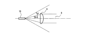
この問題について、図16、図17を用いて説明する。図16は半導体レーザ光源から出射されるレーザ光とコリメータレンズによって取り込まれる光量との関係を示す図、図17は半導体レーザ光源から出射されるレーザ光の広がり角に対する光強度分布を示す図である。図17から分かるように、半導体レーザ光源10から出射されるレーザ光の光強度は、コリメータレンズ9の中心から光束半径が増加するにつれてガウス関数的に減少する。従って、従来においては、対物レンズの開口半径内に入る平行光束8内の強度分布を可能な限り一様に近づけるために、コリメータレンズ9の半径rc及び焦点距離fcを調整(すなわち、コリメータレンズ9の取り込みNA=rc/fcを調整)することにより、半導体レーザ光源10から出射されるレーザ光のうち、角度θdよりも内部のレーザ光だけを対物レンズの開口に取り込むようにされていた。
【0007】
当然ながら、コリメータレンズ9の取り込みNAを小さくすればするほど平行光束8内の強度分布は少なくなるが、半導体レーザ光源から出射されるレーザ光の利用効率は低下する。従って、コリメータレンズ9の取り込みNAは、平行光束8内の強度分布とレーザ光の利用効率のバランスを考慮して決定される。通常、この値は0.2程度に設計されている。上記したように、次世代光ディスクシステムにおいては、DVDシステムよりも高密度化するために対物レンズの開口数NAが0.85まで大きくされ、かつ、波長405nmの半導体レーザ光源が用いられる。
【0008】
一方、レンズ作製用のガラス硝材は、光源波長が短波長化されるにつれて、波長の変化に対する屈折率の変化の度合いが大きくなる。通常、レンズに用いられるガラス硝材の、光源波長が405nm近傍で1nm変化した場合の屈折率の変化は、DVD再生波長650nm近傍での変化量の約3〜4倍程度もある。
【0009】
波長405nmの半導体レーザ光源の温度が変化すると、発振波長が変動するので、対物レンズの屈折率が変化する。そして、これにより、対物レンズの屈折率が設計時の屈折率からずれるので、対物レンズによる、集光スポットの光ディスク表面からの移動量は、DVDの場合の約3〜4倍となる(対物レンズの色収差)。また、レンズは外周部ほど光線を強く曲げるので、対物レンズの外周部を通る光線ほど屈折率の変化の影響を大きく受ける。従って、上記した対物レンズの色収差により、対物レンズの外周部を通る光線ほどフォーカス移動が強く起こり、近軸光線のフォーカス移動はほとんど起こらない。
【0010】
一方、高密度化のために対物レンズのNAを大きくすると、焦点深度は、NAの2乗に反比例して浅くなる。従って、NA0.85のシステムの焦点深度は、NA0.6のシステムの焦点深度の1/2しかない。
【0011】
よって、次世代光ディスクシステム(NA0.85、光源波長405nm)での色収差による焦点移動は、DVDシステムの場合の8倍厳しくなる。従って、次世代光ディスクシステムにおいては、この光源波長の変動による焦点位置の移動にも注意を払う必要がある。この焦点位置の移動が10msec以上の時間をかけて起こる場合には、フォーカス誤差検出法によってフォーカス移動を検出し、それに応じて対物レンズを移動させれば、このフォーカス移動を打ち消すことができるので、光源波長の変動による焦点位置の移動は問題とならないが、焦点位置の移動が10msec以下の時間で起こる場合には、例えば、半導体レーザ光源の記録/再生切り替え時にフォーカスがずれて記録再生が上手く行かず、大きな問題となる。
【0012】
図18に示すように、この色収差を低減するためには、対物レンズ1は、2群3枚のレンズ1c、1f、1eによって構成される。ここで、レンズ1cは凸レンズ、レンズ1fは凹レンズであるから、半導体レーザ光源の発振波長が中心波長405nmよりも短くなると、凸レンズを構成するガラス硝材の屈折率は僅かであるが増加する。従って、凸レンズ2b、1c、1eは、光線を強く曲げるようになるので、光ディスク3の信号面に集光されていた集光スポット4はレンズ1e側に移動することになる。一方、半導体レーザ光源の発振波長が中心波長405nmよりも長くなった場合には、凸レンズを構成するガラス硝材の屈折率は低下する。従って、凸レンズ2b、1c、1eは、光線を曲げる力が弱くなるので、光ディスク3の信号面に集光されていた集光スポット4はレンズ1eと反対側に移動することになる。
【0013】
一方、凹レンズ2a、1fは、光線に対して凸レンズ2b、1c、1eと逆の作用をするので、半導体レーザ光源の発振波長が変動した場合に、凸レンズ2b、1c、1eによる光線の変化を、凹レンズ2a、1fによる光線の変化によって打ち消すことにより、集光スポット4の移動を抑えることができる。この半導体レーザ光源の発振波長の変動による集光スポット4の移動量は、レンズ球面の曲率が大きければ大きいほど大きくなる。従って、凸レンズ2b、1c、1eによる集光スポット4の移動は、ほとんど曲率の大きい凹レンズ1fによって打ち消される。よって、このような2群3枚のレンズ1c、1f、1eによって対物レンズ1を構成することにより、半導体レーザ光源の発振波長が405nmから1nm変化しても、光ディスク3の信号面からの集光スポット4の移動量を0.001μm程度に収めることができる。しかし、このようなレンズ構成の場合には、CDシステム、DVDシステムの単レンズからなる対物レンズに比べてレンズが2枚増加するので、調整工程が複雑になる。また、対物レンズ1を図19に示すような単レンズ構造にすると、組み立て工程の簡素化とレンズ枚数の削減によりコストダウンを図ることはできるが、色収差による集光スポット4の移動量は0.5μmにもなる。従って、この場合には、色収差を低減するために何らかの素子を追加する必要がある。
【0014】
図20に示す光ヘッド装置においては、コストダウンを図るために2枚構成の対物レンズ1が用いられている。この構成によれば、コストダウンが図られるだけでなく、1枚構成の対物レンズの場合よりも色収差が低減される。しかし、それでも、色収差による集光スポット4の移動量は0.35μm程度になり、やはり色収差を低減するために何らかの素子を付加する必要がある。
【0015】
図19、図20に示すような対物レンズ1を用いる場合には、半導体レーザ光源の発振波長の変動時に発生する色収差を低減するために、回折格子からなる色収差補正素子7が挿入される。この場合、図18に示す2群3枚構成の対物レンズ1と比較してレンズ一点あるいは二点が削減され、色収差補正素子7が追加されることになる。しかし、この色収差補正素子7は、ビームエキスパンダ2を構成する凸レンズ2bを樹脂成形によって作るときの一面を利用して簡単に形成することができるので、図18に示す2群3枚構成の対物レンズ1を用いる場合と比較してかなりのコストダウンが見込まれる。
【0016】
このような色収差低減法は、従来から広く知られているが(例えば、特許文献1 以下『第1の従来例』という)、対物レンズの色収差量が大きくなれば、色収差補正素子7の格子ピッチが細かくなる。
【0017】
この色収差補正素子7によって色収差を低減できる理由は、以下の通りである。すなわち、上記したように、例えば、半導体レーザ光源の発振波長が中心波長405nmよりも短くなると、凸レンズを構成するガラス硝材の屈折率が大きくなり、凸レンズのパワーが大きくなるために、光線が強く曲げられて、焦点距離が短くなる。一方、色収差補正素子7を構成する回折格子での波長λと回折角θhとの関係は、θh=λ/p(pは回折格子の格子ピッチ)であるから、波長が短くなると、回折角は小さくなる。従って、色収差補正素子7は、光線に対して凸レンズと逆の作用をする。よって、このような色収差補正素子7を挿入することにより、波長変動に起因して対物レンズ1により引き起こされる焦点移動を打ち消すことが可能となる。この場合、回折角の波長依存性を利用しているので、補正すべき色収差量が大きければ大きいほど、波長変動に対する回折角θhを大きくする必要がある。従って、対物レンズ1の色収差量が大きくなれば、色収差補正素子7の格子ピッチは細かくなり、かつ、内周近軸になるほど色収差補正素子7の格子ピッチは粗くなる。
【0018】
上記したように、2枚構成の対物レンズ1を用いた場合の色収差による集光スポット4の移動量は0.35μm程度であり、この色収差を打ち消すための色収差補正素子7の格子ピッチは、対物レンズ1の有効径最外周部では6μm程度、中心部では150μm程度となる。このように格子ピッチが大幅に変化すると、色収差補正素子7の各半径位置における回折効率は図2Aの実線のように変化する。従って、対物レンズ1の中心付近の光線は、150μmピッチの回折格子によって色消しされるから、この部分の回折効率は99%である。一方、対物レンズ1の有効径最外周部の光線は、6.5μmピッチの回折格子によって色消しされるから、この部分の回折効率は92%程度になる(このピッチに対する回折効率は、理論値から実際起こり得る加工誤差による低下量を見込んだ値となっている)。
【0019】
次に、第2の従来例として、特許文献2に開示されたものを、図21を用いて説明する。図21において、41は光ディスク、42は半導体レーザ光源である。43は回折光431を、入射ビーム光軸に対して斜め方向に、かつ、他の光学素子に入射しないように分岐するホログラムである。半導体レーザ光源42から出射され、ホログラム43に入射したレーザ光は、回折されることにより、中心近傍の光強度が一定である光ビームに変換され、ホログラム43を透過(0次回折)する。尚、ホログラム面を構成する格子上面形状は滑らかな曲線を有する。45はホログラム43を透過した中心近傍の光強度が一定である光ビームを光ディスク41上に集光して、集光スポットを形成するための対物レンズである。ホログラム43による回折によって、中心近傍の光強度が一定である光ビームになるので、対物レンズ45によって集光されて、光ディスク41上に形成される集光スポットの径を、1/e2 幅が0.96λ/NAに略等しい小さなものとすることができる。
【0020】
【特許文献1】特開2001−60336号公報
【0021】
【特許文献2】特開平7−262594号公報
【0022】
【発明が解決しようとする課題】
対物レンズ1で発生する色収差を補正するための色収差補正素子7は、外周部に向かって格子ピッチが小さくなり、また、外周部に向かって回折効率が低下する。従って、対物レンズ1の外周部付近の光強度は、半導体レーザ光源の強度が光束半径距離に対してガウス関数的に低下することと相俟って大幅に低下する。
【0023】
対物レンズの外周部で光強度が大幅に低下すると、対物レンズの実効NAが低下し、その結果、光線が光ディスク上で十分絞れなくなって、NAに比例して光ディスク上の記録密度を上げることはできなかった。
【0024】
また、第2の従来例では、回折光431を、入射ビーム光軸に対して斜め方向に、かつ、他の光学素子に入射しないように分岐するため、回折角度を大きくする必要がある。その結果、ホログラム43の格子ピッチが2μm以下の非常に細かいものとなり、作製が困難であるという問題があった。また、中心近傍の光強度が一定となるようにされている。さらに、半導体レーザ光源42から出射される光ビーム421は、中心の強度が最も強く、外周に行くにしたがって徐々に光量が弱くなるいわゆるガウス分布となっている。従って、ホログラム43の回折効率は、中心点において最も高く、すなわち、0次の透過率が低く、外周に行くにしたがって徐々に低く、すなわち、0次の透過率が高くなるものでなければならない。このように、ホログラム43の回折効率が場所によって変化しているので、光ビーム421の光強度中心との位置ずれがあると、0次の透過光の光量分布が顕著に変化し、もくろみ通りに小さな集光スポットを光ディスク上に形成することが困難であるという問題があった。
【0025】
本発明は、従来技術における前記課題を解決するためになされたものであり、対物レンズの開口数(NA)を大きくして光ディスク上の集光スポットの径を小さくし、光ディスクシステムの高密度化を達成することができ、かつ、高い光利用効率を得ることのできる光ヘッド装置及びそれを用いた光情報装置、並びにこれらを応用したシステムを提供することを目的とする。
【0026】
【課題を解決するための手段】
前記目的を達成するため、本発明に係る光ヘッド装置の第1の構成は、半導体レーザ光源から出射されたレーザ光を、対物レンズを用いて光情報媒体上に集光する集光光学系を有する光ヘッド装置であって、前記半導体レーザ光源と前記光情報媒体との間に、前記対物レンズで発生する色収差を補正する色収差補正素子が設けられており、かつ、前記対物レンズの開口面に入射する光の強度が前記開口面の中心からの距離と共に低下することを補正するために、前記対物レンズの前記開口面の中心からの距離と共に透過率が増加する光分布補正素子が設けられていることを特徴とする。
【0027】
前記本発明の光ヘッド装置の第1の構成においては、前記光分布補正素子が位相段差を有する同心円状の回折格子であるのが好ましい。また、この場合には、前記色収差補正素子と前記光分布補正素子とが1枚のレンズの両面にそれぞれ形成されているのが好ましい。
【0028】
また、本発明に係る光ヘッド装置の第2の構成は、半導体レーザ光源から出射されたレーザ光を、対物レンズを用いて光情報媒体上に集光する集光光学系を有する光ヘッド装置であって、前記半導体レーザ光源と前記光情報媒体との間に、前記対物レンズ開口面に入射する光の強度が前記開口面の中心からの距離と共に低下することを補正するために、前記対物レンズの前記開口面の中心付近の透過率を一定量低下させる光分布補正素子が設けられていることを特徴とする。
【0029】
前記本発明の光ヘッド装置の第2の構成においては、前記光分布補正素子の、透過率の低下する部分が金属蒸着膜によって形成されているのが好ましい。
【0030】
前記本発明の光ヘッド装置の第2の構成においては、前記光分布補正素子の、透過率の低下する部分がホログラムによって形成されているのが好ましい。
【0031】
前記本発明の光ヘッド装置の第2の構成においては、前記光分布補正素子の、透過率の低下する部分が誘電体の多層膜によって形成されているのが好ましい。
【0032】
前記本発明の光ヘッド装置の第2の構成においては、前記光分布補正素子の、透過率の低下する部分の当該透過率が65%〜85%の範囲にあるのが好ましい。
【0033】
前記本発明の光ヘッド装置の第2の構成においては、前記半導体レーザ光源と前記光情報媒体との間に前記対物レンズで発生する色収差を補正する色収差補正素子がさらに設けられており、かつ、前記光分布補正素子の、透過率の低下する部分の当該透過率が60%〜75%の範囲にあるのが好ましい。
【0034】
前記本発明の光ヘッド装置の第1又は第2の構成においては、前記光情報媒体で反射した光を検出する光検出器と、前記光情報媒体で反射した光を前記半導体レーザ光源の方向から分岐して前記光検出器に導く光路分岐手段とをさらに備え、前記光分布補正素子が、前記半導体レーザ光源と前記光路分岐手段との間に配置されているのが好ましい。
【0035】
また、本発明に係る光ヘッド装置の第3の構成は、半導体レーザ光源から出射されたレーザ光を、対物レンズを用いて光情報媒体上に集光する集光光学系を有する光ヘッド装置であって、前記半導体レーザ光源と前記光情報媒体との間に、前記対物レンズ開口面に入射する光の強度が前記開口面の中心からの距離と共に低下することを補正するために、前記対物レンズの前記開口面の中心付近の反射率を一定量低下させる光分布補正素子が設けられていることを特徴とする。
【0036】
前記本発明の光ヘッド装置の第3の構成においては、前記光分布補正素子の、反射率の低下する部分が誘電体の多層膜によって形成されているのが好ましい。
【0037】
前記本発明の光ヘッド装置の第3の構成においては、前記光分布補正素子の、反射率の低下する部分の反射率が65%〜85%の範囲にあるのが好ましい。
【0038】
前記本発明の光ヘッド装置の第3の構成においては、前記半導体レーザ光源と前記光情報媒体との間に前記対物レンズで発生する色収差を補正する色収差補正素子がさらに設けられており、かつ、前記光分布補正素子の、反射率の低下する部分の反射率が60%〜75%の範囲にあるのが好ましい。
【0039】
前記本発明の光ヘッド装置の第3の構成においては、前記光情報媒体で反射した光を検出する光検出器と、前記光情報媒体で反射した光を前記半導体レーザ光源の方向から分岐して前記光検出器に導く光路分岐手段とをさらに備え、前記光分布補正素子が、前記光路分岐手段と前記光情報媒体との間に配置されているのが好ましい。
【0040】
また、本発明に係る光ヘッド装置の第4の構成は、半導体レーザ光源から出射されたレーザ光を、対物レンズを用いて光情報媒体上に集光する集光光学系を有する光ヘッド装置であって、前記半導体レーザ光源と前記光情報媒体との間に前記対物レンズで発生する色収差を補正するレリーフ型のブレーズ格子からなる色収差補正素子が設けられており、かつ、前記対物レンズの開口面に入射する光の強度が前記開口面の中心からの距離と共に低下することを補正するために、前記色収差補正素子の、前記対物レンズの開口面の中心付近に対応する部分の前記ブレーズ格子の高さが、回折効率が最大となる高さとは異なる高さに設定されていることを特徴とする。
【0041】
前記本発明の光ヘッド装置の第4の構成においては、前記色収差補正素子と前記対物レンズとが一体的に固定されているのが好ましい。また、この場合には、前記色収差補正素子が前記対物レンズの表面に一体形成されているのが好ましい。
【0042】
前記本発明の光ヘッド装置の第1、第2、第3又は第4の構成においては、光分布補正を行わない場合と比較して、前記半導体レーザ光源から前記集光光学系へと至る開口数が大きく設定されているのが好ましい。
【0043】
また、本発明に係る光ヘッド装置の第5の構成は、半導体レーザ光源から出射されたレーザ光を、対物レンズを用いて光情報媒体上に集光する集光光学系を有する光ヘッド装置であって、前記半導体レーザ光源と前記光情報媒体との間に、前記対物レンズの開口面に入射する光の強度が前記開口面の中心からの距離と共に低下することを補正するために、前記対物レンズの前記開口面の中心付近の透過率を一定量低下させる光分布補正素子を設け、前記光分布補正素子により損失された前記対物レンズの前記開口面の中心付近の光を用いて、前記光源から出射される光のパワーをモニターすることを特徴とする。
【0044】
また、本発明に係る光ヘッド装置の第6の構成は、半導体レーザ光源から出射されたレーザ光を、対物レンズを用いて光情報媒体上に集光する集光光学系を有する光ヘッド装置であって、前記半導体レーザ光源と前記光情報媒体との間に、前記対物レンズの開口面に入射する光の強度が前記開口面の中心からの距離と共に低下することを補正するために、前記対物レンズの前記開口面の中心付近の反射率を一定量低下させる光分布補正素子を設け、前記光分布補正素子により損失された前記対物レンズの前記開口面の中心付近の光を用いて、前記光源から出射される光のパワーをモニターすることを特徴とする。
【0045】
また、本発明に係る光情報装置の構成は、前記本発明の光ヘッド装置と、前記光情報媒体を駆動する光情報媒体駆動部と、前記光ヘッド装置から得られる信号を受け、前記信号に基づいて、前記光情報媒体駆動部、並びに前記光ヘッド装置内の前記半導体レーザ光源及び対物レンズを制御する制御部とを備えていることを特徴とする。
【0046】
また、本発明に係るコンピュータの構成は、前記本発明の光情報装置と、情報の入力を行う入力装置と、前記入力装置から入力された情報や前記光情報装置によって読み出された情報に基づいて演算を行う演算装置と、前記入力装置から入力された情報や前記光情報装置によって読み出された情報や前記演算装置によって演算された結果を表示あるいは出力する出力装置とを備えていることを特徴とする。
【0047】
また、本発明に係る光ディスクプレーヤの構成は、前記本発明の光情報装置と、前記光情報装置から得られる情報信号を画像に変換する、情報から画像への変換装置とを備えていることを特徴とする。
【0048】
また、本発明に係るカーナビゲーションシステムの構成は、前記本発明の光ディスクプレーヤを備えていることを特徴とする。
【0049】
また、本発明に係る光ディスクレコーダの構成は、前記本発明の光情報装置と、画像情報を、前記光情報装置によって前記光情報媒体へ記録する情報に変換する、画像から情報への変換装置とを備えていることを特徴とする。
【0050】
また、本発明に係る光ディスクサーバの構成は、前記本発明の光情報装置と、外部との情報のやりとりを行う入出力端子とを備えていることを特徴とする。
【0051】
【発明の実施の形態】
以下、実施の形態を用いて本発明をさらに具体的に説明する。
【0052】
[第1の実施の形態]
図1は本発明の第1の実施の形態における光ヘッド装置を示す概略構成図である。
【0053】
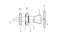
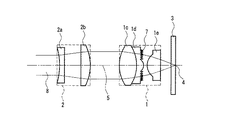
図1に示すように、本実施の形態の光ヘッド装置は、半導体レーザ光源10から出射されたレーザ光を、対物レンズ1を用いて光ディスク(光情報媒体)3上に集光する集光光学系を有している。ここで、対物レンズ1は、半導体レーザ光源10側から順に配置された凸レンズ1aと凸レンズ1bとにより構成されている(2枚構成)。
【0054】
半導体レーザ光源10と対物レンズ1との間には、半導体レーザ光源10側から順に配置された凸レンズ2aと凸レンズ2bとからなるビームエキスパンダ2が設けられている。このようにビームエキスパンダ2が挿入されているのは、以下の理由による。すなわち、光ディスクシステムの高密度化を図るために対物レンズ1の開口数(NA)を大きくすると、光ディスク3の保護層の厚み誤差により、光ディスク3上の集光スポット4の大きさが球面収差のために変化する。そこで、ビームエキスパンダ2を挿入し、その入射側凹レンズ2aと出射側凸レンズ2bとの間隔を変化させることにより、この球面収差を補正するようにされている。また、ビームエキスパンダ2は、対物レンズ1の開口半径とコリメータレンズ9からの平行光束8の光束径とを整合させるために挿入されている。
【0055】
ビームエキスパンダ2を構成する凸レンズ2bの凹レンズ2a側の面には、対物レンズ1で発生する色収差を補正するために、回折格子からなる色収差補素子7が形成されている。
【0056】
このように、本実施の形態においては、対物レンズ1で発生する色収差が、ビームエキスパンダ2を構成する凸レンズ2aに形成された色収差補素子7によって補正され、半導体レーザ光源10に記録/再生切り替え時のレーザ出力変化を与えた場合にも、光ディスク3上の集光スポット4がフォーカス移動しないようにされている。しかし、従来の技術の項で述べたように、色収差補正素子7は、光束の半径方向に向かってピッチが細かくなり、最短ピッチ長は光束の最外周部で6μm程度になり、回折効率も90%程度まで低下する。一方、半導体レーザ光源10から出射された発散光(レーザ光)は、コリメータレンズ9によって平行光束8に変換される。この場合には、図16に示すように、コリメータレンズ9によるレーザ光の取り込み角としてレーザ光の広がり角θよりも小さい角度θdが取られ、光軸上の光強度に対してレンズ有効径最外周部における光強度ができるだけ低下しないようにされている。従って、レーザ光の取り込み角θdを小さくすればするほどリム強度は高くなるが、コリメータレンズ9におけるレーザ光の伝達効率は悪くなる。この方法によれば、確かに、色収差補正素子7を用いて、外周部で発生する回折効率の低下による光量分布の低下の問題も解決することはできる。しかし、この方法では、光量ロスがかなり大きくなるという問題がある。
【0057】
そこで、本実施の形態においては、この問題を解決するために、ビームエキスパンダ2を構成する凸レンズ2bの対物レンズ1側の面に、対物レンズ1の開口面の中心(光軸)からの距離と共に透過率が増加する回折格子からなる光分布補正素子6が形成されている。色収差補正素子7は、中央部で回折効率が高く、周辺部に行くにしたがって回折効率が低下し、これにより光量分布が生じる。すなわち、対物レンズ1の開口面に入射する光の強度が前記開口面の中心からの距離と共に低下する。これを補正するためには、中央部で透過率が低く、周辺部に行くにしたがって透過率が高くなるような光分布補正素子6を形成する必要がある。光分布補正素子6としては、例えば、中心部では回折効率が高くなるような溝深さを有し、周辺部に行くほど溝深さが浅くなる位相型回折格子を形成すればよい。また、回折格子の凸面と凹面の1ピッチ内での比を変えることによっても、対物レンズ1の開口面に入射する光の強度が前記開口面の中心からの距離と共に低下することを補正することができる。この場合には、周辺部では凸面と凹面の比を1よりも大きくするか小さくし、中心部に行くほどこの比を1に近づけることにより、中心部に行くほど、回折効率を高め、透過率を低下させることができる。
【0058】
さらに、光分布補正素子6の回折効率を一定にし、当該光分布補正素子6を凸レンズ2bの中心部のみに形成することにより、光軸に対する光分布補正素子6の位置誤差の許容度を高めることができる。そして、これにより、光ヘッド装置の組み立てが容易になるという顕著な効果が得られる。
【0059】
また、回折格子を同心円状として、光分布補正素子6にレンズ効果を持たせることも効果的である。この場合、回折光は、光ディスク3上において透過光が収束するときにはデフォーカスし、不要な情報を持って反射してくることがない。従って、第2の従来例のように格子ピッチを細かくして回折角度を大きくする必要がなく、光分布補正素子6の製造が容易となる。
【0060】
また、光分布の補正は、例えば、クロム(Cr)や銀(Ag)といった金属の蒸着膜が中心部分にのみ形成されたフィルタからなる光分布補正素子を用いることによっても実現することができる。ここで、金属蒸着膜を形成する領域の大きさ、すなわち、金属蒸着膜の直径は、凸レンズ2bの直径の1/2以上、3/4以下であるのが望ましい。この場合にも当然、第2の従来例のように細かいピッチの格子を形成する必要がなく、光分布補正素子6の製造が容易となる。
【0061】
光分布補正素子6の中心部分(金属蒸着膜が形成されて透過率が一定量低下している部分)の透過率は、光分布補正素子6を色収差補正素子7と同時に用いない場合には、65%〜85%程度であるのが望ましい。これは、中心部分の光量を用いなくなる光量ロスを、コリメータレンズ9による取り込みNAを大きくする効果が上回り、全体として光利用効率を高めることができるという効果が得られる値である。
【0062】
また、光分布補正素子6の中心部分(金属蒸着膜が形成されて透過率が一定量低下している部分)の透過率は、光分布補正素子6を色収差補正素子7と同時に用いる場合には、60%〜75%程度であるのが望ましい。これは、上記した、光分布補正素子6を色収差補正素子7と同時に用いない場合に対してさらに1割程度、色収差補正素子による外周部の透過率低下を補正する効果が得られる値である。
【0063】
このように光分布補正素子6を形成することにより、光分布補正素子6を、色収差補正素子7との一体成形で作製することもできる。これにより、色収差補正素子7と光分布補正素子6の中心合わせを5μm程度で行うことが可能となり、色収差補正素子7による外周部の光量低下を補うという観点からは、より正確にプロファイル補正を行うことが可能となる。この光分布補正素子6によって光分布の補正を行えば、従来の、コリメータレンズ9の取り込みNAを小さくして光量分布を平坦にする方法よりも、半導体レーザ光源10から出射されるレーザ光の利用効率を大幅に改善することができる。
【0064】
また、本実施の形態の光ヘッド装置においては、半導体レーザ光源10から光ディスク3へと至る光路(往路)と、光ディスク3で反射した光が光検出器12へと至る光路(復路)とを分岐するための光路分岐手段としての偏光ビームスプリッタ13が設けられている。尚、光路分岐手段としては、偏光ビームスプリッタ13以外に、ハーフミラーや回折素子等を用いることもできる。この場合、光分布補正素子6を、半導体レーザ光源10と光路分岐手段との間に挿入することにより、光分布補正素子6が往路にのみ作用し、復路には作用しないようにして、復路の光利用効率を高め、信号対雑音比(S/N)を高めて安定な信号再生を実現することもできる。尚、図1中、5は対物レンズ1への入射光を示している。
【0065】
一例として、コリメータレンズ9の取り込みNAを小さくして光分布を補正した場合と、光分布補正素子6によって光分布を補正した場合とで、いずれの方式が、半導体レーザ光源10から出射されるレーザ光の利用効率を改善できるかを、シミュレーションによって算出した。尚、光ディスクシステムの記録再生実験により、対物レンズ1の最外周での光強度が中心部での光強度の60%よりも小さくなると、記録再生信号の品質が劣化し始めることが判明している。このため、対物レンズ1の最外周での光強度として中心部での光強度の60%以上を確保するとの条件でシミュレーションを行っている。
【0066】
まず、色収差補正素子7と光分布補正回折格子6が存在しない場合には、対物レンズ3の有効径が3.4mm、レーザ光の広がり角が27度、コリメータレンズ9の取り込みNAが0.2、対物レンズ1の最外周での光強度が中心部での光強度の60%であるとき、半導体レーザ光源10から出射されるレーザ光の利用効率は40%であった。次に、上記条件の下で色収差補正素子7のみを挿入した場合には、半導体レーザ光源10から出射されるレーザ光の利用効率は37.8%まで低下し、対物レンズ1の最外周での光強度は中心部での光強度の56%まで低下した。但し、色収差補正素子7は、有効最大径位置での格子ピッチが6.5μm、回折効率が91%、中心部での回折効率が98%になるとしている。
【0067】
このように色収差補正素子7のみを挿入した場合には、対物レンズ1の最外周での光強度が中心部での光強度の60%よりも小さくなるので、これを補正して60%以上とするために、まず、コリメータレンズ9の取り込みNAを、0.2から0.188まで小さくした。しかし、この場合には、半導体レーザ光源10から出射されるレーザ光の利用効率は、さらに33.7%まで低下した。
【0068】
次に、本実施の形態の光分布補正素子6を挿入して、対物レンズ1の最外周での光強度を中心部での光強度の60%以上にした。この場合、半導体レーザ光源10から出射されるレーザ光の利用効率は、36.2%となった。
【0069】
但し、光分布補正素子6の回折効率は、以下のように設定されている。すなわち、色収差補正素子7の中心部に対向する位置での光分布補正素子6の回折効率は91.5%、色収差補正素子7の格子ピッチが15μmである位置に対向する位置での光分布補正素子6の回折効率は91.3%、色収差補正素子7の格子ピッチが10μmである位置に対向する位置での光分布補正素子6の回折効率は91.1%、色収差補正素子7の格子ピッチが6.5μmである位置に対向する位置での光分布補正素子6の回折効率は100%に設定されている。
【0070】
図2Aに、色収差補正素子の光軸中心からの距離と回折効率及び格子ピッチとの関係を示し、図2Bに、本実施の形態の光分布補正素子の光軸中心からの距離と回折効率及び格子ピッチとの関係を示す。
【0071】
半導体レーザ光源10から出射されるレーザ光の利用効率は、従来の方式(コリメータレンズ9の取り込みNAを小さくする方式)では33.7%であるが、本実施の形態の方式では36.2%となり、光分布補正素子6を挿入することにより、3%(従来の方式での33.7%を基準に考えると、約1割)の改善が見込まれる。この値は小さいように見えるが、現実の記録再生光ヘッド装置に本実施の形態の方式を適用した場合、必要とされる半導体レーザ光源10の出力光量は大きく変化する。
【0072】
このことについて、例えば、光ディスク3上に情報を記録するときに対物レンズ1からの出力光量として12mW必要とされる場合を例に挙げて説明する。今、色収差補正素子7が存在しない場合に必要とされる半導体レーザ光源10の出力は12/0.4=30mWとなる。
【0073】
このとき、色収差補正素子7で発生する光分布ムラを、本実施の形態の光分布補正素子6によって補正する場合、12/0.36=33mWの半導体レーザ光源10で済む。すなわち、半導体レーザ光源10への負担は10%の増加で済む。
【0074】
しかし、この光分布ムラを、従来のコリメータレンズ9の取り込みNAを小さくすることによって解決しようとすると、必要とされる半導体レーザ光源10の出力は12/0.33=36mWとなり、20%の出力増加が必要となる。すなわち、本実施の形態によれば、光分布補正素子を用いない場合と比較して、半導体レーザ光源10から集光光学系へと至る開口数を大きく設定することにより、光利用効率を高めつつ、外周部の光強度を光軸付近の光強度と同じ程度に保ち、光ディスク3に対する集光性能を確保できるという顕著な効果が得られる。
【0075】
記録時に必要とされる出力光量が50mWであるとき、本実施の形態の方式を適用すれば、レーザ出力が55mWの半導体レーザ光源10で済むが、従来の取り込みNAを下げる方法を用いる場合には、レーザ出力が60mWの半導体レーザ光源10を必要とする。
【0076】
このように、光ディスク3に情報を記録する場合には、一般に、高出力の半導体レーザ光源10が必要となるため、この伝達効率の改善は非常に重要なことである。
【0077】
尚、本実施の形態においては、ビームエキスパンダ2が設けられているが、必ずしもビームエキスパンダ2を設けなくても、所期の効果を得ることができ、ビームエキスパンダ2を設けない構成もあり得る。
【0078】
また、本実施の形態においては、対物レンズ1が、凸レンズ1aと凸レンズ1bとにより構成されているが(2枚構成)、図3に示す1枚構成の場合であっても、原理的には全く同じである。
【0079】
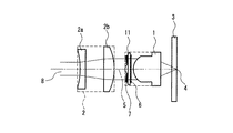
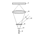
[第2の実施の形態]
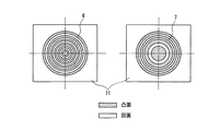
図4は本発明の第2の実施の形態における光ヘッド装置の対物レンズ周りの様子を示す概略構成図、図5は光分布補正素子と色収差補正素子を示す平面図である。
【0080】
図4、図5に示すように、本実施の形態においては、ビームエキスパンダ2とは別体の一枚の成形板11の両面に、それぞれ光分布補正素子6と色収差補正素子7とが同時成形によって形成されている。そして、この成形板11は、対物レンズ1に一体的に固定されている。このため、対物レンズ1が光ディスク3上の情報溝に沿って横方向に移動しても、対物レンズ1の中心と色収差補正素子7の中心及び光分布補正素子6の中心とがずれることはない。従って、色収差補正素子7も必要以上に細かいピッチの所を使用することが無くなり、素子の作製も簡単になる。また、格子ピッチの拡大により、光利用効率の向上も達成することができる。
【0081】
光分布補正素子6に必要とされる半径方向の回折効率は、図2Bに示すようにほとんど一定であるため、回折格子の溝深さを変える必要はないが、もし半径方向の回折効率を大幅に変える必要がある場合には、回折格子の溝深さを変えてもよい。そして、もし回折格子の溝深さの変化によって透過光の位相が問題となった場合には、この位相を補正するように、対物レンズ1の形状かビームエキスパンダ2を構成するレンズの形状を変えればよい。
【0082】
さらにまた、光分布の補正は、対物レンズ1の表面の反射を防止するために形成される反射防止膜(ARコート)の設計を変更することによっても実現することができる。対物レンズ1のNAを大きくする場合には、図1に示すように、対物レンズ1の半導体レーザ光源10側の面(例えば、レンズ1aの図中で左側の凸面)の曲率を大きくする必要がある。このため、光線の入射角度が、光軸付近と最外周とで大きく異なる。例えば、対物レンズ1のNAを0.85とした場合、光軸付近と最外周では光線の入射角度が約40度以上異なる。ARコートの反射率は光線の入射角度に依存して変化するので、最外周での光線の入射角度に対して反射率が最も低く透過率が最も高くなるように設計すれば、光軸付近の内周部では反射が起こり、透過率が低下する。さらに、半導体レーザ光源10からコリメートレンズ9に至るNAを大きくすることにより、光利用効率の向上と、集光性能の向上、すなわち、光記録密度の向上とを、部品点数も加工の工数も増やすことなく実現できるという効果が得られる。このようにARコートの設計を工夫することは、特開2001−6204号公報にも開示されているが、本願における『さらに光源からコリメートレンズへと至るNAを大きくすることにより、光利用効率の向上を実現する』という構成は開示されていない。
【0083】
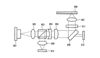
また、光分布補正素子は、上記以外の他の方法で実現することもできる。図6に、本発明の第2の実施の形態における上記以外の光分布補正素子を用いた光ヘッド装置の概略構成を示す。図6に示すように、この光ヘッド装置は、半導体レーザ光源901から出射されたレーザ光を、対物レンズ907を用いて光ディスク908上に集光する集光光学系を有している。半導体レーザ光源901と対物レンズ907との間には、半導体レーザ光源901側から順に配置された凹レンズ904と凸レンズ905とからなるビームエキスパンダが設けられている。
【0084】
また、ビームエキスパンダと対物レンズ907との間には、誘電体の多層膜(例えば、SiO2 と酸化チタンを交互に複数層積層したものを用いることができる)で形成されたミラーからなる光分布補正素子906が配置されている。この光分布補正素子(ミラー)906は、偏光方向に応じて反射率が異なる。例えば、その所定部(光軸付近の内周部)の反射率は、P偏光に対してK1、S偏光に対してはK2になっている。また、所定部以外(所定部の外周部)の反射率は、P偏光及びS偏光ともにK3になっている。本実施の形態においては、K1=70%、K2=K3=100%に設定されている。
【0085】
また、この光ヘッド装置においては、半導体レーザ光源901から光ディスク908へと至る光路(往路)と、光ディスク908で反射した光が光検出器910へと至る光路(復路)とを分岐するための光路分岐手段としての偏光ビームスプリッタ903が設けられている。尚、図6中、902は半導体レーザ光源901から出射された発散光(レーザ光)を平行光束に変換するコリメータレンズ、909は集光レンズ、911はL/4波長板(Lは1以上の奇数)である。また、912は往路の光のうち、光分布補正素子906を透過した光を受光する光検出器である。
【0086】
以下、このように構成された光ヘッド装置の動作について、図6を参照しながら説明する。半導体レーザ光源901から出射された直線偏光の光(偏光方向は光分布補正素子906に対してP偏光となる方向)は、コリメータレンズ902によって平行光束に変換される。コリメータレンズ902を透過した光は、さらに偏光ビームスプリッタ903を透過した後、凹レンズ904によって発散光となる。そして、この発散光は、凸レンズ905によって平行光束に変換され、光分布補正素子906で反射されて、その進行方向が90度曲げられる。光分布補正素子906によって進行方向が曲げられた光は、L/4波長板911によって円偏光に変換された後、対物レンズ907によって光ディスク908上に集光される。
【0087】
次に、光ディスク908で反射された光は、対物レンズ907を透過した後、L/4波長板911によって半導体レーザ光源901から出射された光の偏光方向と直交する方向の光に変換される。L/4波長板911を透過した光は、光分布補正素子906で反射され、凸レンズ905、凹レンズ904を順次透過した後、偏光ビームスプリッタ903で反射されて、集光レンズ909により光検出器910に集光される。そして、光検出器910は、光ディスク908上における光の合焦状態を示すフォーカス誤差信号を出力し、また、光の照射位置を示すトラッキング誤差信号を出力する。ここで、フォーカス誤差信号とトラッキング誤差信号は、周知の技術、例えば、非点収差法とプッシュプル法等によって検出される。フォーカス制御手段(図示せず)は、フォーカス誤差信号に基づいて、常に光が合焦状態で光ディスク908上に集光されるように、対物レンズ907の位置をその光軸方向に制御する。また、トラッキング制御手段(図示せず)は、トラッキング誤差信号に基づいて、光が光ディスク908上の所望のトラックに集光されるように、対物レンズ907の位置を制御する。また、光検出器910からは、光ディスク908に記録された情報も得られる。
【0088】
ここで、光分布補正素子906は上記したような反射率特性を有しているので、往路に対しては光軸付近の内周部の反射率が下がることになり、その結果、相対的に対物レンズ907の最外周での光強度を上げることが可能となる。また、復路に対しては光分布補正素子906の反射率が場所によらず一様となっているので、光分布補正素子906は通常のミラーとなる。
【0089】
以上のように、誘電体の多層膜で形成され、上記のような反射率特性を有するミラーを用いることによっても、光分布の補正を行うことが可能となる。また、第2の従来例のように格子ピッチを細かくする必要がないので、光分布補正素子906の製造が容易となる。尚、この光分布補正素子906は、上記した透過型の光分布補正素子と異なり、反射型のものである。
【0090】
また、光分布補正素子906が対物レンズ907に近い位置にあるので、光強度分布の中心と対物レンズ907の中心とを合わせる調整を行えば、所定部(光軸付近の内周部)の中心と光強度分布の中心とのずれが小さくなる。その結果、光分布補正素子906の位置調整を行わずに光ヘッド装置を組み立てることが可能となる。さらに、往路の光のうち、光分布補正素子906の光軸付近の内周部を透過した光を光検出器912によって受光することにより、半導体レーザ光源901から出射される光のパワーがモニターされる。この構成を採用することにより、半導体レーザ光源901から出射される光のパワーを、記録や再生に用いられない光を使ってモニターすることが可能となるので、光の利用効率の高い光ヘッド装置を実現することが可能となる。
【0091】
また、本構成においては、光を分岐する偏光ビームスプリッタ903と光ディスク908との間に光分布補正素子906が配置されているが、光分布補正素子906は偏光方向に応じて反射率が異なっているので、復路での光量ロスは起こらない。
【0092】
光分布補正素子906の中心部分の反射率は、光分布補正素子906を色収差補正素子と同時に用いない場合には、上記第1の実施の形態と同様に65%〜85%程度であるのが望ましい。これは、中心部分の光量を用いなくなる光量ロスを、コリメータレンズ902による取り込みNAを大きくする効果が上回り、全体として光利用効率を高めることができるという効果が得られる値である。
【0093】
光分布補正素子906の中心部分の反射率は、光分布補正素子906を色収差補正素子と同時に用いる場合には、上記第1の実施の形態と同様に60%〜75%程度であるのが望ましい。これは、上記した、光分布補正素子906を色収差補正素子と同時に用いない場合に対してさらに1割程度、色収差補正素子による外周部の透過効率低下を補正する効果が得られる値である。
【0094】
また、上記以外の光分布補正素子として、ガラス板の中央部分にのみホログラムを形成し、当該部分の透過率を下げた光学素子も考えられる。ここで、ホログラムを形成した部分を透過した光とホログラムを形成した部分以外の部分を透過した光の位相が異なり、光ヘッド装置の特性が損なわれる場合には、位相合わせを行えばよい。この位相合わせは、例えば、図7Aに示すように、ホログラム913を形成した部分以外の部分の厚さを薄くすることによって実現することができる。また、位相合わせを行う別の方法としては、例えば、図7Bに示すように、ホログラム913を形成した部分の裏面に薄膜914(例えば、SiO2 を単層で用いることができる)を設ける方法もある。尚、他の方法で位相合わせを行っても何ら問題はない。また、ガラス板の中央部分にのみ誘電体の多層膜を形成して、当該部分の透過率を下げてもよい。
【0095】
また、上記においては、光分布補正素子906の光軸付近の内周部を透過した光を光検出器912によって受光することにより、半導体レーザ光源901から出射される光のパワーをモニターする場合について説明したが、光分布補正素子906以外の光分布補正素子を用いた場合であっても、半導体レーザ光源901から出射される光のパワーをモニターすることは可能である。例えば、ホログラムを形成し、その部分の透過率を下げて光分布を補正する素子(図1の2bや図7)の場合には、その回折光を用いて半導体レーザ光源から出射される光のパワーをモニターすることが可能である。また、金属蒸着膜を形成し、その部分の透過率を下げて光分布を補正する素子の場合には、その反射光を用いて半導体レーザ光源から出射される光のパワーをモニターすることが可能である。尚、上記した回折光や反射光を受光するために、その光の進行方向を変えるための光学素子(例えば、ミラー)を用いてもよい。また、記録や再生のための光学系に使用されている光学素子を用いて光の進行方向を変えても何ら問題はない。この場合、回折光や反射光を受光するための光検出器の位置を任意に設定できるので、光ヘッド装置の設計上有利である。
【0096】
[第3の実施の形態]
光分布補正素子を、色収差補正素子と兼ねることも可能である。以下、このことについて、図8を用いて説明する。図8はビームエキスパンダを構成する凸レンズを示す概略断面図である。図8に示すように、凸レンズ2bの左側の面には、対物レンズで発生する色収差を補正するために、レリーフ型のブレーズ格子(鋸歯状のブレーズホログラム)からなる色収差補正素子7bが一体に形成されている。ここで、対物レンズの開口面の中心付近に対応する部分のブレーズ格子の高さは、回折効率が最大となる高さよりも低くなっており、これにより、色収差補正素子7bの中心付近の回折効率が低くされている。従って、別途、光分布補正素子を設けることなく、光分布の補正を行って、集光スポットの径の縮小と光利用効率の向上を実現することができると共に、部品点数の削減を図ることもできる。
【0097】
また、図9に示すように、対物レンズの開口面の中心付近に対応する部分のブレーズ格子の高さを、回折効率が最大となる高さよりも高くすることによって、色収差補正素子7cの回折効率を低くするようにしてもよい。
【0098】
[第4の実施の形態]
対物レンズ1が組み合わせレンズである場合には、図10に示すように、光分布補正素子を、組み合わせレンズを構成する個別のレンズ(例えば、レンズ1dと1e)の間に配置しても構わない。さらに、レンズ(例えば、図10では1d)表面に光分布補正素子を兼ねた色収差補正素子7を形成することにより、部品点数の削減を図ることができる。
【0099】
[第5の実施の形態]
図11は本発明の第5の実施の形態における光情報装置を示す概略構成図である。図11に示すように、光ディスク3は、ターンテーブル82に載せられ、光情報媒体駆動部としてのモータ64によって回転駆動される(光ディスク3の代わりに光カードを用いる場合には、当該光カードは並進駆動される)。55は上記第1〜第4の実施の形態に示した光ヘッド装置であり、当該光ヘッド装置55は、光ディスク3の所望の情報が存在するトラックのところまで、光ヘッド装置の駆動装置51によって粗動される。
【0100】
また、光ヘッド装置55は、光ディスク3との位置関係に対応して、フォーカスエラー信号やトラッキングエラー信号を、制御部としての電気回路53へ送る。電気回路53は、これらの信号に基づいて、対物レンズを微動させるための信号を光ヘッド装置55へ送る。そして、光ヘッド装置55は、この信号に基づいて、光ディスク3に対しフォーカス制御とトラッキング制御を行った後、情報の読み出し、書き込み(記録)又は消去を行う。また、この電気回路53は、光ヘッド装置55から得られる信号に基づいてモータ64や光ヘッド装置55内の半導体レーザ光源をも制御する。
【0101】
本実施の形態の光情報装置67においては、光ヘッド装置55として、上記第1〜第4の実施の形態に示した光ヘッド装置が用いられているので、微小な集光スポットを光ディスク3上に形成することができ、高い記録密度の光ディスクに対して記録や再生を行うことができる。
【0102】
[第6の実施の形態]
図12は本発明の第6の実施の形態におけるコンピュータを示す概略斜視図である。
【0103】
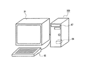
図12に示すように、本実施の形態のコンピュータ100は、上記第5の実施の形態の光情報装置67と、情報の入力を行うためのキーボードあるいはマウス、タッチパネルなどの入力装置65と、入力装置65から入力された情報や、光情報装置67によって読み出された情報などに基づいて演算を行う中央演算装置(CPU)などの演算装置84と、演算装置84によって演算された結果などの情報を表示あるいは出力するための陰極線管装置、液晶表示装置、プリンタなどの出力装置81とを備えている。
【0104】
[第7の実施の形態]
図13は本発明の第7の実施の形態における光ディスクプレーヤを示す概略斜視図である。
【0105】
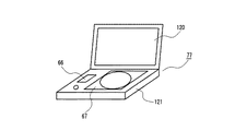
図13に示すように、本実施の形態の光ディスクプレーヤ121は、上記第5の実施の形態の光情報装置67と、光情報装置67から得られる情報信号を画像に変換する、情報から画像への変換装置(例えば、デコーダ66)とを備えている。
【0106】
尚、本構成は、カーナビゲーションシステムとしても利用することができる。また、液晶モニタなどの表示装置120を付加した構成とすることも可能である。
【0107】
[第8の実施の形態]
図14は本発明の第8の実施の形態における光ディスクレコーダを示す概略斜視図である。
【0108】
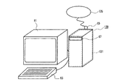
図14に示すように、本実施の形態の光ディスクレコーダ110は、上記第5の実施の形態の光情報装置67と、画像情報を、光情報装置67によって光ディスクへ記録する情報に変換する、画像から情報への変換装置(例えば、エンコーダ68)とを備えている。
【0109】
尚、光情報装置67から得られる情報信号を画像に変換する、情報から画像への変換装置(例えば、デコーダ66)を付加した構成とすることも可能であり、これにより既に記録した部分を再生することも可能となる。
【0110】
また、情報を表示する陰極線管装置、液晶表示装置、プリンタなどの出力装置81を付加した構成とすることも可能である。
【0111】
上記第5の実施の形態の光情報装置67を備えた、あるいは、上記の記録・再生方法を採用したコンピュータ、光ディスクプレーヤ、光ディスクレコーダは、高い記録密度の光ディスクに対して記録や再生を行うことができるので、より多くの情報を蓄えたり扱ったりすることが可能となる。
【0112】
[第9の実施の形態]
図15は本発明の第9の実施の形態における光ディスクサーバを示す概略斜視図である。
【0113】
図15に示すように、本実施の形態の光ディスクサーバ130は、上記第5の実施の形態の光情報装置67と、光情報装置67に記録する情報を取り込んだり、光情報装置67によって読み出された情報を外部に出力したりするための有線又は無線の入出力端子69とを備えている。
【0114】
以上の構成により、光ディスクサーバ130は、ネットワーク135、すなわち、複数の機器、例えば、コンピュータ、電話、テレビチューナなどと情報をやりとりし、これら複数の機器に対する共有の情報サーバとして利用することが可能となる。また、異なる種類の光ディスクに対して安定に記録や再生を行うことができるので、広い用途に使用することができる。
【0115】
また、情報を表示する陰極線管装置、液晶表示装置、プリンタなどの出力装置81を付加した構成とすることも可能である。
【0116】
さらに、複数の光ディスクを光情報装置67に出し入れするチェンジャー131を付加した構成とすることにより、多くの情報を記録・蓄積しておくこともできる。
【0117】
尚、上記第6〜第9の実施の形態において、図12〜図15には出力装置81や液晶モニタ120を示しているが、出力端子を備えるだけで、出力装置81や液晶モニタ120を持たず、これらを別売りとする商品形態があり得ることは言うまでもない。また、図13と図14には入力装置は図示されていないが、キーボード、タッチパネル、マウス、リモートコントロール装置などの入力装置を備えた商品形態もあり得る。逆に、上記第6及び第9の実施の形態においては、入力装置を別売りとし、入力端子のみを備えた形態もあり得る。
【0118】
また、本発明における光情報媒体として、光ディスクの代わりに光カードを用いた場合であっても、光ディスクを用いた場合と同等の効果を得ることができる。すなわち、本発明は、微小な集光スポットを形成することにより、記録あるいは再生が行われる光情報媒体のすべてについて適用可能である。
【0119】
【発明の効果】
以上説明したように、本発明によれば、対物レンズの開口数(NA)を大きくして光ディスク上の集光スポットの径を小さくし、光ディスクシステムの高密度化を達成することのできる光ヘッド装置を実現することができる。そして、この場合、記録再生光ヘッドに必要な半導体レーザ出力を、従来の取り込みNAを低下させる方法よりも一割程度あるいはそれ以上低減することができる。すなわち、光利用効率を向上させることができる。
【図面の簡単な説明】
【図1】本発明の第1の実施の形態における光ヘッド装置を示す概略構成図
【図2】図2Aは色収差補正素子の光軸中心からの距離と格子ピッチ及び回折効率との関係を示す図、図2Bは本発明の第1の実施の形態における光分布補正素子の光軸中心からの距離と格子ピッチ及び回折効率との関係を示す図
【図3】本発明の第1の実施の形態における光ヘッド装置の他の例の対物レンズ周りの様子を示す概略構成図
【図4】本発明の第2の実施の形態における光ヘッド装置の対物レンズ周りの様子を示す概略構成図
【図5】本発明の第2の実施の形態における光分布補正素子と色収差補正素子を示す平面図
【図6】本発明の第2の実施の形態における光ヘッド装置の他の例を示す概略構成図
【図7】図7Aは本発明の第2の実施の形態における光分布補正素子の他の例を示す概略断面図、図7Bは本発明の第2の実施の形態における光分布補正素子のさらに他の例を示す概略断面図
【図8】本発明の第3の実施の形態における光分布補正素子を兼ねた色収差補正素子が形成されたレンズを示す概略断面図
【図9】本発明の第3の実施の形態における光分布補正素子を兼ねた色収差補正素子が形成されたレンズの他の例を示す概略断面図
【図10】本発明の第4の実施の形態における光ヘッド装置の対物レンズ周りの様子を示す概略構成図
【図11】本発明の第5の実施の形態における光情報装置を示す概略構成図
【図12】本発明の第6の実施の形態におけるコンピュータを示す概略斜視図
【図13】本発明の第7の実施の形態における光ディスクプレーヤを示す概略斜視図
【図14】本発明の第8の実施の形態における光ディスクレコーダを示す概略斜視図
【図15】本発明の第9の実施の形態における光ディスクサーバを示す概略斜視図
【図16】従来技術における、半導体レーザ光源から出射されるレーザ光とコリメータレンズによって取り込まれる光量との関係を示す図
【図17】従来技術における、半導体レーザ光源から出射されるレーザ光の広がり角に対する光強度分布を示す図
【図18】従来技術における、2群3枚構成の対物レンズを有する光ヘッド装置の対物レンズ周りの様子を示す概略構成図
【図19】従来技術における、単レンズ構造の対物レンズを有する光ヘッド装置の対物レンズ周りの様子を示す概略構成図
【図20】従来技術における、2枚構成の対物レンズを有する光ヘッド装置の対物レンズ周りの様子を示す概略構成図
【図21】従来技術における光ヘッド装置の他の例を示す要部概略断面図
【符号の説明】
1、907 対物レンズ
1a、1b、1c、1d、1e 対物レンズを構成する単レンズ
2 ビームエキスパンダ
2a、2b ビームエキスパンダを構成する単レンズ
3、908 光ディスク
4 集光スポット
5 対物レンズへの入射光
6、906 光分布補正素子
7 色収差補正素子
8 平行光束
9、902 コリメータレンズ
10、901 半導体レーザ光源
12、910 光検出器
13、903 偏光ビームスプリッタ
51 光ヘッド装置の駆動装置
53 電気回路
55 光ヘッド装置
64 モータ
65 入力装置
66 デコーダ
67 光情報装置
68 エンコーダ
69 入出力端子
77 光ディスクプレーヤ
81 出力装置
84 演算装置
100 コンピュータ
110 光ディスクレコーダ
130 光ディスクサーバ
913 ホログラム[0001]
TECHNICAL FIELD OF THE INVENTION
The present invention relates to an optical head device used for recording information on an optical information medium or reproducing information recorded on the optical information medium, and an optical information device using the same (including a recording / reproducing device and a reproduction-only device). ) As well as systems applying these.
[0002]
[Prior art]
2. Description of the Related Art In recent years, there has been active development for increasing the numerical aperture (NA) of an objective lens to reduce the diameter of a condensed spot on an optical disk and achieving a higher density optical disk system. For example, the NA of an objective lens in a CD system is 0.4 and the NA of an objective lens in a DVD system is 0.6, while the NA of an objective lens of a next-generation optical disk system is expected to be as large as 0.85. ing. At this time, the in-plane distribution of light incident on the aperture of the objective lens becomes a problem.
[0003]
This can be explained as follows. Now, if the in-plane distribution of the light incident on the opening of the objective lens is constant, the diameter of the light spot focused on the optical disk by the objective lens is given by λ / NA. Here, λ is the wavelength of the light source. Further, the relationship of NA = r / f holds. Here, r is the aperture radius of the objective lens, and f is the focal length of the objective lens.
[0004]
The aperture radius r and the focal length f are originally determined by the physical dimensions of the objective lens. For example, when the amount of light becomes 0 near the aperture, the substantial aperture radius is determined by the physical size of the objective lens. It can be easily inferred that the opening radius becomes smaller than the typical opening radius. Therefore, even if an attempt is made to increase the density of the optical disk system by increasing the NA of the objective lens, that is, to reduce the diameter of the condensed spot on the optical disk, the surface of the light incident on the aperture of the objective lens is reduced. If the inner distribution is not as uniform as possible, high densification cannot be achieved.
[0005]
Conventionally, there has been a problem that the in-plane distribution of light incident on the aperture of the objective lens is not uniform. This occurs because the light intensity of the laser light emitted from the semiconductor laser light source is not uniform in the light beam.
[0006]
This problem will be described with reference to FIGS. FIG. 16 is a diagram showing the relationship between the laser light emitted from the semiconductor laser light source and the amount of light taken in by the collimator lens, and FIG. 17 is a diagram showing the light intensity distribution with respect to the spread angle of the laser light emitted from the semiconductor laser light source. . As can be seen from FIG. 17, the light intensity of the laser light emitted from the semiconductor
[0007]
Naturally, as the capture NA of the
[0008]
On the other hand, the degree of change in the refractive index of a glass glass material for producing a lens with respect to a change in the wavelength increases as the wavelength of the light source becomes shorter. Normally, the change in the refractive index of the glass material used for the lens when the light source wavelength changes by 1 nm near 405 nm is about 3 to 4 times the change amount near the DVD reproduction wavelength of 650 nm.
[0009]
When the temperature of the semiconductor laser light source having a wavelength of 405 nm changes, the oscillation wavelength changes, so that the refractive index of the objective lens changes. Since the refractive index of the objective lens deviates from the refractive index at the time of design, the amount of movement of the condensed spot from the optical disk surface by the objective lens is about 3 to 4 times that of a DVD (objective lens). Chromatic aberration). Also, since the lens bends the light beam more strongly at the outer peripheral portion, the light beam passing through the outer peripheral portion of the objective lens is greatly affected by the change in the refractive index. Therefore, due to the chromatic aberration of the objective lens described above, the focus movement occurs more strongly as the light beam passes through the outer peripheral portion of the objective lens, and the focus movement of the paraxial light beam hardly occurs.
[0010]
On the other hand, when the NA of the objective lens is increased for higher density, the depth of focus becomes shallower in inverse proportion to the square of NA. Therefore, the depth of focus of the system with NA of 0.85 is only half the depth of focus of the system with NA of 0.6.
[0011]
Therefore, in the next-generation optical disk system (NA 0.85, light source wavelength 405 nm), the focal point shift due to chromatic aberration is eight times as severe as in the DVD system. Therefore, in the next-generation optical disk system, it is necessary to pay attention to the movement of the focal position due to the fluctuation of the light source wavelength. If the movement of the focus position takes a time of 10 msec or more, the focus movement can be canceled by detecting the focus movement by the focus error detection method and moving the objective lens accordingly. Although the movement of the focal position due to the fluctuation of the light source wavelength is not a problem, if the movement of the focal position occurs within 10 msec or less, for example, when the recording / reproducing switching of the semiconductor laser light source is performed, the focus is shifted and the recording / reproducing is performed well. It is a big problem.
[0012]
As shown in FIG. 18, in order to reduce this chromatic aberration, the
[0013]
On the other hand, since the
[0014]
In the optical head device shown in FIG. 20, a two-piece
[0015]
When the
[0016]
Such a chromatic aberration reduction method has been widely known (for example, refer to
[0017]
The reason why the chromatic aberration can be reduced by the chromatic
[0018]
As described above, the amount of movement of the condensed spot 4 due to chromatic aberration when the two-piece
[0019]
Next, a second conventional example disclosed in
[0020]
[Patent Document 1] Japanese Patent Application Laid-Open No. 2001-60336
[0021]
[Patent Document 2] JP-A-7-262594
[0022]
[Problems to be solved by the invention]
In the chromatic
[0023]
When the light intensity decreases significantly at the outer periphery of the objective lens, the effective NA of the objective lens decreases, and as a result, the light beam cannot be sufficiently focused on the optical disc, and the recording density on the optical disc increases in proportion to the NA. could not.
[0024]
Further, in the second conventional example, the diffracted
[0025]
SUMMARY OF THE INVENTION The present invention has been made to solve the above-mentioned problems in the prior art, and increases the numerical aperture (NA) of an objective lens to reduce the diameter of a condensed spot on an optical disk, thereby increasing the density of an optical disk system. It is an object of the present invention to provide an optical head device, an optical information device using the optical head device, and a system using the optical head device, which can achieve high light utilization efficiency.
[0026]
[Means for Solving the Problems]
In order to achieve the above object, a first configuration of an optical head device according to the present invention includes a focusing optical system that focuses laser light emitted from a semiconductor laser light source on an optical information medium using an objective lens. An optical head device, wherein a chromatic aberration correction element for correcting chromatic aberration generated in the objective lens is provided between the semiconductor laser light source and the optical information medium, and the chromatic aberration correction element is provided on an opening surface of the objective lens. In order to correct that the intensity of the incident light decreases with the distance from the center of the aperture surface, a light distribution correction element is provided in which the transmittance increases with the distance from the center of the aperture surface of the objective lens. It is characterized by having.
[0027]
In the first configuration of the optical head device according to the present invention, it is preferable that the light distribution correction element is a concentric diffraction grating having a phase step. In this case, it is preferable that the chromatic aberration correction element and the light distribution correction element are formed on both surfaces of one lens.
[0028]
A second configuration of the optical head device according to the present invention is an optical head device having a condensing optical system that condenses laser light emitted from a semiconductor laser light source on an optical information medium using an objective lens. Between the semiconductor laser light source and the optical information medium, the objective lens for correcting that the intensity of light incident on the objective lens aperture surface decreases with the distance from the center of the aperture surface. And a light distribution correction element for reducing the transmittance near the center of the opening surface by a certain amount.
[0029]
In the second configuration of the optical head device according to the present invention, it is preferable that a portion of the light distribution correction element, whose transmittance is reduced, is formed of a metal deposition film.
[0030]
In the second configuration of the optical head device according to the present invention, it is preferable that a portion of the light distribution correction element where the transmittance is reduced is formed by a hologram.
[0031]
In the second configuration of the optical head device according to the present invention, it is preferable that a portion of the light distribution correction element where the transmittance is reduced is formed of a dielectric multilayer film.
[0032]
In the second configuration of the optical head device of the present invention, it is preferable that the transmittance of the light distribution correction element in a portion where the transmittance is reduced is in a range of 65% to 85%.
[0033]
In the second configuration of the optical head device of the present invention, a chromatic aberration correction element for correcting chromatic aberration generated in the objective lens is further provided between the semiconductor laser light source and the optical information medium, and It is preferable that the transmittance of the portion of the light distribution correction element where the transmittance decreases is in the range of 60% to 75%.
[0034]
In the first or second configuration of the optical head device of the present invention, a light detector for detecting light reflected on the optical information medium, and a light reflected on the optical information medium from a direction of the semiconductor laser light source. It is preferable that the apparatus further includes an optical path branching unit that branches and guides the light to the photodetector, and the light distribution correction element is disposed between the semiconductor laser light source and the optical path branching unit.
[0035]
A third configuration of the optical head device according to the present invention is an optical head device having a condensing optical system that condenses laser light emitted from a semiconductor laser light source on an optical information medium using an objective lens. Between the semiconductor laser light source and the optical information medium, the objective lens for correcting that the intensity of light incident on the objective lens aperture surface decreases with the distance from the center of the aperture surface. A light distribution correction element for reducing the reflectance near the center of the aperture surface by a certain amount is provided.
[0036]
In the third configuration of the optical head device according to the present invention, it is preferable that a portion of the light distribution correction element where the reflectance is reduced is formed of a dielectric multilayer film.
[0037]
In the third configuration of the optical head device of the present invention, it is preferable that the reflectance of the light distribution correction element at a portion where the reflectance is reduced is in a range of 65% to 85%.
[0038]
In the third configuration of the optical head device of the present invention, a chromatic aberration correction element for correcting chromatic aberration generated in the objective lens is further provided between the semiconductor laser light source and the optical information medium, and It is preferable that the reflectance of a portion where the reflectance of the light distribution correction element decreases is in the range of 60% to 75%.
[0039]
In the third configuration of the optical head device according to the present invention, a light detector that detects light reflected by the optical information medium, and a light beam that reflects light reflected by the optical information medium is branched from a direction of the semiconductor laser light source. It is preferable that the apparatus further includes an optical path branching unit that guides the light to the photodetector, and the light distribution correction element is disposed between the optical path branching unit and the optical information medium.
[0040]
Further, a fourth configuration of the optical head device according to the present invention is an optical head device having a condensing optical system that condenses laser light emitted from a semiconductor laser light source on an optical information medium using an objective lens. A chromatic aberration correction element comprising a relief-type blazed grating for correcting chromatic aberration generated in the objective lens is provided between the semiconductor laser light source and the optical information medium; and an aperture surface of the objective lens Height of the blazed grating in a portion of the chromatic aberration correction element corresponding to the vicinity of the center of the aperture surface of the objective lens, in order to correct that the intensity of light incident on the aperture surface decreases with the distance from the center of the aperture surface. Is set to a height different from the height at which the diffraction efficiency is maximized.
[0041]
In the fourth configuration of the optical head device according to the present invention, it is preferable that the chromatic aberration correction element and the objective lens are fixed integrally. In this case, it is preferable that the chromatic aberration correction element is formed integrally with the surface of the objective lens.
[0042]
In the first, second, third or fourth configuration of the optical head device according to the present invention, an aperture extending from the semiconductor laser light source to the condensing optical system is compared with a case where light distribution correction is not performed. Preferably, the number is set large.
[0043]
A fifth configuration of the optical head device according to the present invention is an optical head device having a condensing optical system that condenses laser light emitted from a semiconductor laser light source on an optical information medium using an objective lens. Between the semiconductor laser light source and the optical information medium, in order to correct that the intensity of light incident on the aperture surface of the objective lens decreases with the distance from the center of the aperture surface, A light distribution correction element for reducing a transmittance of the lens in the vicinity of the center of the opening surface by a certain amount; and using the light near the center of the opening surface of the objective lens lost by the light distribution correction element, the light source The power of the light emitted from is monitored.
[0044]
A sixth configuration of the optical head device according to the present invention is an optical head device having a condensing optical system that condenses laser light emitted from a semiconductor laser light source on an optical information medium using an objective lens. Between the semiconductor laser light source and the optical information medium, in order to correct that the intensity of light incident on the aperture surface of the objective lens decreases with the distance from the center of the aperture surface, A light distribution correction element for reducing the reflectance near the center of the aperture surface of the lens by a certain amount; and using the light near the center of the aperture surface of the objective lens lost by the light distribution correction element, the light source The power of the light emitted from is monitored.
[0045]
Further, the configuration of the optical information device according to the present invention is such that the optical head device of the present invention, an optical information medium drive unit that drives the optical information medium, and a signal obtained from the optical head device, The optical information medium driving unit, and a control unit for controlling the semiconductor laser light source and the objective lens in the optical head device.
[0046]
Also, the configuration of the computer according to the present invention is based on the optical information device of the present invention, an input device for inputting information, and information input from the input device or information read by the optical information device. And an output device for displaying or outputting information input from the input device, information read by the optical information device, or a result calculated by the arithmetic device. Features.
[0047]
Also, the configuration of the optical disc player according to the present invention includes the optical information device of the present invention, and an information-to-image conversion device that converts an information signal obtained from the optical information device into an image. Features.
[0048]
Further, a configuration of a car navigation system according to the present invention includes the optical disc player of the present invention.
[0049]
Further, the configuration of the optical disc recorder according to the present invention, the optical information device of the present invention, the image information is converted into information to be recorded on the optical information medium by the optical information device, an image-to-information conversion device, It is characterized by having.
[0050]
Further, a configuration of an optical disc server according to the present invention is characterized by including the optical information device of the present invention and an input / output terminal for exchanging information with the outside.
[0051]
BEST MODE FOR CARRYING OUT THE INVENTION
Hereinafter, the present invention will be described more specifically with reference to embodiments.
[0052]
[First Embodiment]
FIG. 1 is a schematic configuration diagram showing an optical head device according to the first embodiment of the present invention.
[0053]
As shown in FIG. 1, the optical head device of the present embodiment is a condensing optic that condenses laser light emitted from a semiconductor
[0054]
Between the semiconductor
[0055]
On the surface of the
[0056]
As described above, in the present embodiment, the chromatic aberration generated in the
[0057]
Therefore, in the present embodiment, in order to solve this problem, the surface of the
[0058]
Furthermore, by making the diffraction efficiency of the light distribution correction element 6 constant and forming the light distribution correction element 6 only at the center of the
[0059]
It is also effective to make the diffraction grating concentric so that the light distribution correction element 6 has a lens effect. In this case, the diffracted light is defocused when the transmitted light converges on the optical disc 3, and is not reflected with unnecessary information. Therefore, it is not necessary to increase the diffraction angle by reducing the grating pitch as in the second conventional example, and the manufacture of the light distribution correction element 6 is facilitated.
[0060]
Further, the correction of the light distribution can also be realized by using a light distribution correction element composed of a filter in which a deposited film of a metal such as chromium (Cr) or silver (Ag) is formed only in the central portion. Here, it is desirable that the size of the region where the metal vapor deposition film is formed, that is, the diameter of the metal vapor deposition film is 以上 or more and / or less of the diameter of the
[0061]
When the light distribution correction element 6 is not used simultaneously with the chromatic
[0062]
The transmittance of the central portion of the light distribution correction element 6 (the portion where the transmittance is reduced by a certain amount due to the formation of the metal deposition film) is determined when the light distribution correction element 6 is used simultaneously with the chromatic
[0063]
By forming the light distribution correction element 6 in this way, the light distribution correction element 6 can be manufactured by integral molding with the chromatic
[0064]
Further, in the optical head device of the present embodiment, the optical path (outgoing path) from the semiconductor
[0065]
As an example, either of a method in which the light distribution is corrected by reducing the capture NA of the
[0066]
First, when the chromatic
[0067]
When only the chromatic
[0068]
Next, the light distribution correction element 6 of the present embodiment was inserted so that the light intensity at the outermost periphery of the
[0069]
However, the diffraction efficiency of the light distribution correction element 6 is set as follows. In other words, the light distribution correction element 6 has a diffraction efficiency of 91.5% at a position facing the center of the chromatic
[0070]
FIG. 2A shows the relationship between the distance from the optical axis center of the chromatic aberration correction element and the diffraction efficiency and the grating pitch. FIG. 2B shows the distance from the optical axis center and the diffraction efficiency of the light distribution correction element of the present embodiment. This shows the relationship with the lattice pitch.
[0071]
The utilization efficiency of the laser light emitted from the semiconductor
[0072]
This will be described by taking, as an example, a case where 12 mW is required as the output light amount from the
[0073]
At this time, when the light distribution unevenness generated by the chromatic
[0074]
However, if this light distribution unevenness is to be solved by reducing the input NA of the
[0075]
When the output light quantity required at the time of recording is 50 mW, if the method of the present embodiment is applied, the semiconductor
[0076]
As described above, when information is recorded on the optical disc 3, a high-output semiconductor
[0077]
Although the
[0078]
Further, in the present embodiment, the
[0079]
[Second embodiment]
FIG. 4 is a schematic configuration diagram showing a state around an objective lens of an optical head device according to a second embodiment of the present invention, and FIG. 5 is a plan view showing a light distribution correction element and a chromatic aberration correction element.
[0080]
As shown in FIGS. 4 and 5, in the present embodiment, the light distribution correction element 6 and the chromatic
[0081]
Since the diffraction efficiency in the radial direction required for the light distribution correction element 6 is almost constant as shown in FIG. 2B, it is not necessary to change the groove depth of the diffraction grating. When it is necessary to change the groove depth, the groove depth of the diffraction grating may be changed. If the phase of the transmitted light becomes a problem due to a change in the groove depth of the diffraction grating, the shape of the
[0082]
Furthermore, the correction of the light distribution can also be realized by changing the design of an anti-reflection film (AR coat) formed to prevent reflection on the surface of the
[0083]
Further, the light distribution correction element can be realized by other methods than the above. FIG. 6 shows a schematic configuration of an optical head device using a light distribution correction element other than the above in the second embodiment of the present invention. As shown in FIG. 6, the optical head device has a condensing optical system that condenses laser light emitted from a semiconductor
[0084]
Further, between the beam expander and the
[0085]
Further, in this optical head device, an optical path for branching an optical path (outward path) from the semiconductor
[0086]
Hereinafter, the operation of the optical head device thus configured will be described with reference to FIG. Linearly polarized light (the direction of polarization becomes P-polarized with respect to the light distribution correction element 906) emitted from the semiconductor
[0087]
Next, the light reflected by the
[0088]
Here, since the light
[0089]
As described above, it is also possible to correct the light distribution by using a mirror formed of a dielectric multilayer film and having the above-described reflectance characteristics. Further, since it is not necessary to make the grating pitch fine as in the second conventional example, the manufacture of the light
[0090]
In addition, since the light
[0091]
In this configuration, the light
[0092]
When the light
[0093]
When the light
[0094]
In addition, an optical element in which a hologram is formed only in the central portion of the glass plate and the transmittance of the portion is reduced as a light distribution correction element other than the above is also conceivable. Here, if the phase of the light transmitted through the portion where the hologram is formed is different from the phase of the light transmitted through the portion other than the portion where the hologram is formed, and the characteristics of the optical head device are impaired, the phases may be adjusted. This phase matching can be realized, for example, by reducing the thickness of a portion other than the portion where the
[0095]
In the above description, the case where the power of the light emitted from the semiconductor
[0096]
[Third Embodiment]
The light distribution correction element can also serve as the chromatic aberration correction element. Hereinafter, this will be described with reference to FIG. FIG. 8 is a schematic sectional view showing a convex lens constituting the beam expander. As shown in FIG. 8, on the left surface of the
[0097]
Further, as shown in FIG. 9, the height of the blaze grating in a portion corresponding to the vicinity of the center of the aperture surface of the objective lens is made higher than the height at which the diffraction efficiency is maximized, so that the diffraction efficiency of the chromatic aberration correction element 7c is increased. May be lowered.
[0098]
[Fourth Embodiment]
When the
[0099]
[Fifth Embodiment]
FIG. 11 is a schematic configuration diagram showing an optical information device according to the fifth embodiment of the present invention. As shown in FIG. 11, the optical disk 3 is placed on a
[0100]
The
[0101]
In the
[0102]
[Sixth Embodiment]
FIG. 12 is a schematic perspective view showing a computer according to the sixth embodiment of the present invention.
[0103]
As shown in FIG. 12, a
[0104]
[Seventh Embodiment]
FIG. 13 is a schematic perspective view showing an optical disc player according to the seventh embodiment of the present invention.
[0105]
As shown in FIG. 13, an
[0106]
Note that this configuration can also be used as a car navigation system. Further, a configuration in which a
[0107]
[Eighth Embodiment]
FIG. 14 is a schematic perspective view showing an optical disc recorder according to the eighth embodiment of the present invention.
[0108]
As shown in FIG. 14, an optical disc recorder 110 according to the present embodiment includes an
[0109]
Incidentally, it is also possible to add a device for converting an information signal obtained from the
[0110]
Further, it is also possible to adopt a configuration in which an
[0111]
A computer, an optical disk player, and an optical disk recorder that include the
[0112]
[Ninth embodiment]
FIG. 15 is a schematic perspective view showing an optical disk server according to the ninth embodiment of the present invention.
[0113]
As shown in FIG. 15, the
[0114]
With the above configuration, the
[0115]
Further, it is also possible to adopt a configuration in which an
[0116]
Furthermore, by adding a
[0117]
Although the
[0118]
Further, even when an optical card is used as the optical information medium in place of the optical disc as the optical information medium of the present invention, the same effect as when the optical disc is used can be obtained. That is, the present invention is applicable to all optical information media on which recording or reproduction is performed by forming a minute condensed spot.
[0119]
【The invention's effect】
As described above, according to the present invention, an optical head capable of increasing the numerical aperture (NA) of an objective lens, reducing the diameter of a condensed spot on an optical disk, and achieving high density of an optical disk system The device can be realized. In this case, the semiconductor laser output required for the recording / reproducing optical head can be reduced by about 10% or more compared to the conventional method of reducing the capture NA. That is, light use efficiency can be improved.
[Brief description of the drawings]
FIG. 1 is a schematic configuration diagram showing an optical head device according to a first embodiment of the present invention.
FIG. 2A is a diagram showing the relationship between the distance from the optical axis center of the chromatic aberration correction element to the grating pitch and diffraction efficiency, and FIG. 2B is the optical axis of the light distribution correction element according to the first embodiment of the present invention. Diagram showing the relationship between the distance from the center, grating pitch and diffraction efficiency
FIG. 3 is a schematic configuration diagram showing a state around an objective lens of another example of the optical head device according to the first embodiment of the present invention.
FIG. 4 is a schematic configuration diagram showing a state around an objective lens of an optical head device according to a second embodiment of the present invention.
FIG. 5 is a plan view showing a light distribution correction element and a chromatic aberration correction element according to a second embodiment of the present invention.
FIG. 6 is a schematic configuration diagram showing another example of the optical head device according to the second embodiment of the present invention.
FIG. 7A is a schematic cross-sectional view showing another example of the light distribution correction element according to the second embodiment of the present invention, and FIG. 7B is a further view of the light distribution correction element according to the second embodiment of the present invention. Schematic sectional view showing another example
FIG. 8 is a schematic cross-sectional view showing a lens on which a chromatic aberration correction element serving also as a light distribution correction element according to a third embodiment of the present invention is formed.
FIG. 9 is a schematic cross-sectional view showing another example of a lens provided with a chromatic aberration correction element also serving as a light distribution correction element according to the third embodiment of the present invention.
FIG. 10 is a schematic configuration diagram showing a state around an objective lens of an optical head device according to a fourth embodiment of the present invention.
FIG. 11 is a schematic configuration diagram showing an optical information device according to a fifth embodiment of the present invention.
FIG. 12 is a schematic perspective view showing a computer according to a sixth embodiment of the present invention.
FIG. 13 is a schematic perspective view showing an optical disc player according to a seventh embodiment of the present invention.
FIG. 14 is a schematic perspective view showing an optical disc recorder according to an eighth embodiment of the present invention.
FIG. 15 is a schematic perspective view showing an optical disc server according to a ninth embodiment of the present invention.
FIG. 16 is a diagram showing a relationship between laser light emitted from a semiconductor laser light source and the amount of light taken in by a collimator lens according to the related art.
FIG. 17 is a diagram showing a light intensity distribution with respect to a spread angle of laser light emitted from a semiconductor laser light source in a conventional technique.
FIG. 18 is a schematic configuration diagram showing a state around an objective lens of an optical head device having a two-group, three-element objective lens according to the related art.
FIG. 19 is a schematic configuration diagram showing a state around an objective lens of an optical head device having an objective lens having a single-lens structure in a conventional technique.
FIG. 20 is a schematic configuration diagram illustrating a state around an objective lens of an optical head device having a two-piece objective lens according to the related art.
FIG. 21 is a schematic cross-sectional view of a main part showing another example of the optical head device according to the related art.
[Explanation of symbols]
1,907 objective lens
1a, 1b, 1c, 1d, 1e Single lens constituting an objective lens
2 Beam expander
2a, 2b Single lens constituting beam expander
3,908 Optical disk
4 Focusing spot
5 Light incident on objective lens
6,906 Light distribution correction element
7 Chromatic aberration correction element
8 Parallel light flux
9,902 Collimator lens
10,901 Semiconductor laser light source
12,910 Photodetector
13,903 Polarizing beam splitter
51 Driving device for optical head device
53 electric circuit
55 Optical Head Device
64 motor
65 Input device
66 decoder
67 Optical Information Equipment
68 encoder
69 I / O terminal
77 Optical Disc Player
81 Output device
84 arithmetic unit
100 computer
110 Optical Disk Recorder
130 Optical Disk Server
913 Hologram
Claims (27)
前記半導体レーザ光源と前記光情報媒体との間に、前記対物レンズで発生する色収差を補正する色収差補正素子が設けられており、かつ、前記対物レンズの開口面に入射する光の強度が前記開口面の中心からの距離と共に低下することを補正するために、前記対物レンズの前記開口面の中心からの距離と共に透過率が増加する光分布補正素子が設けられていることを特徴とする光ヘッド装置。An optical head device having a condensing optical system that condenses laser light emitted from a semiconductor laser light source on an optical information medium using an objective lens,
A chromatic aberration correction element for correcting chromatic aberration generated in the objective lens is provided between the semiconductor laser light source and the optical information medium, and the intensity of light incident on an aperture surface of the objective lens is An optical head provided with a light distribution correction element whose transmittance increases with the distance from the center of the aperture surface of the objective lens in order to correct the decrease with the distance from the center of the surface. apparatus.
前記半導体レーザ光源と前記光情報媒体との間に、前記対物レンズ開口面に入射する光の強度が前記開口面の中心からの距離と共に低下することを補正するために、前記対物レンズの前記開口面の中心付近の透過率を一定量低下させる光分布補正素子が設けられていることを特徴とする光ヘッド装置。An optical head device having a condensing optical system that condenses laser light emitted from a semiconductor laser light source on an optical information medium using an objective lens,
Between the semiconductor laser light source and the optical information medium, in order to correct that the intensity of light incident on the aperture surface of the objective lens decreases with the distance from the center of the aperture surface, the aperture of the objective lens is corrected. An optical head device comprising a light distribution correction element for reducing a transmittance near a center of a surface by a predetermined amount.
前記光分布補正素子が、前記半導体レーザ光源と前記光路分岐手段との間に配置されている請求項1〜9のいずれかに記載の光ヘッド装置。A light detector that detects light reflected by the optical information medium; andan optical path branching unit that guides the light reflected by the optical information medium from the direction of the semiconductor laser light source to the light detector.
10. The optical head device according to claim 1, wherein the light distribution correction element is disposed between the semiconductor laser light source and the optical path branching unit.
前記半導体レーザ光源と前記光情報媒体との間に、前記対物レンズ開口面に入射する光の強度が前記開口面の中心からの距離と共に低下することを補正するために、前記対物レンズの前記開口面の中心付近の反射率を一定量低下させる光分布補正素子が設けられていることを特徴とする光ヘッド装置。An optical head device having a condensing optical system that condenses laser light emitted from a semiconductor laser light source on an optical information medium using an objective lens,
Between the semiconductor laser light source and the optical information medium, in order to correct that the intensity of light incident on the aperture surface of the objective lens decreases with the distance from the center of the aperture surface, the aperture of the objective lens is corrected. An optical head device comprising a light distribution correction element for reducing a reflectance near a center of a surface by a certain amount.
前記光分布補正素子が、前記光路分岐手段と前記光情報媒体との間に配置されている請求項11〜14のいずれかに記載の光ヘッド装置。A light detector that detects light reflected by the optical information medium; andan optical path branching unit that guides the light reflected by the optical information medium from the direction of the semiconductor laser light source to the light detector.
15. The optical head device according to claim 11, wherein the light distribution correction element is disposed between the optical path branching unit and the optical information medium.
前記半導体レーザ光源と前記光情報媒体との間に前記対物レンズで発生する色収差を補正するレリーフ型のブレーズ格子からなる色収差補正素子が設けられており、かつ、前記対物レンズの開口面に入射する光の強度が前記開口面の中心からの距離と共に低下することを補正するために、前記色収差補正素子の、前記対物レンズの開口面の中心付近に対応する部分の前記ブレーズ格子の高さが、回折効率が最大となる高さとは異なる高さに設定されていることを特徴とする光ヘッド装置。An optical head device having a condensing optical system that condenses laser light emitted from a semiconductor laser light source on an optical information medium using an objective lens,
A chromatic aberration correction element composed of a relief-type blazed grating for correcting chromatic aberration generated in the objective lens is provided between the semiconductor laser light source and the optical information medium, and is incident on an aperture surface of the objective lens. In order to correct that the intensity of light decreases with the distance from the center of the aperture, the height of the blazed grating of the chromatic aberration correction element corresponding to the vicinity of the center of the aperture of the objective lens is: An optical head device wherein a height different from a height at which diffraction efficiency is maximized is set.
前記半導体レーザ光源と前記光情報媒体との間に、前記対物レンズの開口面に入射する光の強度が前記開口面の中心からの距離と共に低下することを補正するために、前記対物レンズの前記開口面の中心付近の透過率を一定量低下させる光分布補正素子を設け、前記光分布補正素子により損失された前記対物レンズの前記開口面の中心付近の光を用いて、前記光源から出射される光のパワーをモニターすることを特徴とする光ヘッド装置。An optical head device having a condensing optical system that condenses laser light emitted from a semiconductor laser light source on an optical information medium using an objective lens,
Between the semiconductor laser light source and the optical information medium, in order to correct that the intensity of light incident on the aperture surface of the objective lens decreases with the distance from the center of the aperture surface, A light distribution correction element for reducing the transmittance near the center of the opening surface by a certain amount is provided, and the light emitted from the light source is emitted using light near the center of the opening surface of the objective lens lost by the light distribution correction element. An optical head device for monitoring the power of light.
前記半導体レーザ光源と前記光情報媒体との間に、前記対物レンズの開口面に入射する光の強度が前記開口面の中心からの距離と共に低下することを補正するために、前記対物レンズの前記開口面の中心付近の反射率を一定量低下させる光分布補正素子を設け、前記光分布補正素子により損失された前記対物レンズの前記開口面の中心付近の光を用いて、前記光源から出射される光のパワーをモニターすることを特徴とする光ヘッド装置。An optical head device having a condensing optical system that condenses laser light emitted from a semiconductor laser light source on an optical information medium using an objective lens,
Between the semiconductor laser light source and the optical information medium, in order to correct that the intensity of light incident on the aperture surface of the objective lens decreases with the distance from the center of the aperture surface, A light distribution correction element for reducing the reflectance near the center of the opening surface by a certain amount is provided, and the light emitted from the light source is emitted by using light near the center of the opening surface of the objective lens lost by the light distribution correction element. An optical head device for monitoring the power of light.
情報の入力を行う入力装置と、
前記入力装置から入力された情報や前記光情報装置によって読み出された情報に基づいて演算を行う演算装置と、
前記入力装置から入力された情報や前記光情報装置によって読み出された情報や前記演算装置によって演算された結果を表示あるいは出力する出力装置とを備えたコンピュータ。An optical information device according to claim 22,
An input device for inputting information;
An arithmetic device that performs an arithmetic operation based on information input from the input device and information read by the optical information device,
A computer comprising: an output device that displays or outputs information input from the input device, information read by the optical information device, or a result calculated by the arithmetic device.
前記光情報装置から得られる情報信号を画像に変換する、情報から画像への変換装置とを備えた光ディスクプレーヤ。An optical information device according to claim 22,
An optical disc player comprising: an information-to-image conversion device for converting an information signal obtained from the optical information device into an image.
画像情報を、前記光情報装置によって前記光情報媒体へ記録する情報に変換する、画像から情報への変換装置とを備えた光ディスクレコーダ。An optical information device according to claim 22,
An optical disk recorder comprising: an image-to-information conversion device for converting image information into information to be recorded on the optical information medium by the optical information device.
外部との情報のやりとりを行う入出力端子とを備えた光ディスクサーバ。An optical information device according to claim 22,
An optical disc server having an input / output terminal for exchanging information with the outside.
Priority Applications (9)
| Application Number | Priority Date | Filing Date | Title |
|---|---|---|---|
| JP2002274085A JP2004145906A (en) | 2001-10-02 | 2002-09-19 | Optical head device and optical information device using the same |
| EP10007244A EP2244258B1 (en) | 2001-10-02 | 2002-10-02 | Focussing optical system |
| DE60237188T DE60237188D1 (en) | 2001-10-02 | 2002-10-02 | Optical head assembly and optical device for using the same |
| EP02022113A EP1300838B8 (en) | 2001-10-02 | 2002-10-02 | Optical head device and optical information apparatus using the same |
| US10/264,297 US7110342B2 (en) | 2001-10-02 | 2002-10-02 | Optical head device and optical information apparatus using the same |
| CNB021442088A CN1244922C (en) | 2001-10-02 | 2002-10-08 | Optical read and write head device and optical information device using said optical read and write head device |
| CN 200510088104 CN1741155B (en) | 2001-10-02 | 2002-10-08 | Optical read and write head device and optical information device using said optical read and write head device |
| US11/443,751 US7330419B2 (en) | 2001-10-02 | 2006-05-31 | Optical head device and optical information apparatus using the same |
| US11/443,750 US7480227B2 (en) | 2001-10-02 | 2006-05-31 | Optical head device and optical information apparatus using the same |
Applications Claiming Priority (3)
| Application Number | Priority Date | Filing Date | Title |
|---|---|---|---|
| JP2001306119 | 2001-10-02 | ||
| JP2002247747 | 2002-08-27 | ||
| JP2002274085A JP2004145906A (en) | 2001-10-02 | 2002-09-19 | Optical head device and optical information device using the same |
Publications (2)
| Publication Number | Publication Date |
|---|---|
| JP2004145906A true JP2004145906A (en) | 2004-05-20 |
| JP2004145906A5 JP2004145906A5 (en) | 2005-10-27 |
Family
ID=27347643
Family Applications (1)
| Application Number | Title | Priority Date | Filing Date |
|---|---|---|---|
| JP2002274085A Withdrawn JP2004145906A (en) | 2001-10-02 | 2002-09-19 | Optical head device and optical information device using the same |
Country Status (5)
| Country | Link |
|---|---|
| US (3) | US7110342B2 (en) |
| EP (2) | EP2244258B1 (en) |
| JP (1) | JP2004145906A (en) |
| CN (1) | CN1244922C (en) |
| DE (1) | DE60237188D1 (en) |
Cited By (4)
| Publication number | Priority date | Publication date | Assignee | Title |
|---|---|---|---|---|
| JP2005018949A (en) * | 2003-06-30 | 2005-01-20 | Koninkl Philips Electronics Nv | Optical system, optical pickup device, device for recording audio and/or image, and/or a device for reproducing audio and/or image |
| US8797834B2 (en) | 2010-06-21 | 2014-08-05 | Panasonic Corporation | Objective lens, optical head, optical disk device, and information processing device |
| JP2016059968A (en) * | 2014-09-12 | 2016-04-25 | キヤノン株式会社 | Manufacturing method of member, optical member, and optical element |
| JP6996089B2 (en) | 2017-02-24 | 2022-02-04 | 株式会社ニコン | Diffractive optical elements, optical systems and optical equipment |
Families Citing this family (18)
| Publication number | Priority date | Publication date | Assignee | Title |
|---|---|---|---|---|
| JP2003215310A (en) * | 2001-11-15 | 2003-07-30 | Konica Corp | Optical lens and optical information recording and reproducing device |
| CN1573361A (en) * | 2003-05-23 | 2005-02-02 | 柯尼卡光学技术株式会社 | Optical lens and optical information recording and reproducing apparatus |
| JP2005031361A (en) * | 2003-07-11 | 2005-02-03 | Konica Minolta Opto Inc | Optical lens and information recording and reproducing apparatus |
| CN1918639A (en) * | 2004-02-05 | 2007-02-21 | 皇家飞利浦电子股份有限公司 | Optical device for recording and reproducing |
| JP4363251B2 (en) * | 2004-05-14 | 2009-11-11 | ソニー株式会社 | Optical pickup and optical disk apparatus |
| KR100651326B1 (en) * | 2004-11-05 | 2006-11-29 | 삼성전기주식회사 | A chromatic aberration correction optical system and optical pick-up device using thereof |
| KR100680171B1 (en) * | 2005-01-25 | 2007-02-08 | 삼성전자주식회사 | Compatible optical pickup |
| JP2006331605A (en) * | 2005-05-30 | 2006-12-07 | Canon Inc | Optical information recording and reproducing apparatus |
| US20080253261A1 (en) * | 2005-09-19 | 2008-10-16 | Arima Devices Corporation | Optical Pickup Having Aberration Correction |
| JP2007115345A (en) * | 2005-10-20 | 2007-05-10 | Sharp Corp | Optical pickup device |
| JP2007293979A (en) * | 2006-04-24 | 2007-11-08 | Sony Corp | Solid immersion lens and condensing lens using the same, optical pickup device and optical recording/reproducing device |
| JP2008165908A (en) * | 2006-12-28 | 2008-07-17 | Matsushita Electric Ind Co Ltd | Objective lens and optical pickup device |
| JP5025349B2 (en) * | 2007-06-25 | 2012-09-12 | 三洋電機株式会社 | Optical pickup device |
| US7898929B2 (en) * | 2007-07-20 | 2011-03-01 | Sanyo Electric Co., Ltd. | Objective lens, and method of manufacturing the same and optical pickup apparatus |
| JP5799686B2 (en) * | 2011-09-07 | 2015-10-28 | ソニー株式会社 | Objective lens, optical pickup device, and optical disk device |
| KR101392072B1 (en) | 2012-05-22 | 2014-05-07 | 액츠 주식회사 | Beam irradiation |
| US9915819B2 (en) * | 2015-06-02 | 2018-03-13 | The Johns Hopkins University | Fiber-optic methods and devices enabling multiphoton imaging with improved signal to-noise ratio |
| US11686938B2 (en) | 2020-12-16 | 2023-06-27 | Samsung Electronics Co., Ltd. | Augmented reality device for providing 3D augmented reality and operating method of the same |
Family Cites Families (14)
| Publication number | Priority date | Publication date | Assignee | Title |
|---|---|---|---|---|
| DE4323971C2 (en) * | 1992-07-16 | 2002-11-07 | Asahi Optical Co Ltd | Read / write device for an optical disk |
| DE69319676T2 (en) * | 1992-08-07 | 1998-12-10 | Matsushita Electric Ind Co Ltd | Optical system and device for image information |
| JP2532818B2 (en) | 1993-02-01 | 1996-09-11 | 松下電器産業株式会社 | Objective lens and optical head device |
| JP3203121B2 (en) | 1994-03-18 | 2001-08-27 | 三洋電機株式会社 | Optical head |
| KR0141159B1 (en) * | 1995-04-17 | 1998-07-01 | 김광호 | Collective house control system |
| US5754512A (en) * | 1995-05-30 | 1998-05-19 | Matsushita Electric Industrial Co., Ltd. | Correction elements to lower light intensity around an optical axis of an optical head with a plurality of focal points |
| US5717674A (en) * | 1995-06-30 | 1998-02-10 | Sanyo Electrics Co., Ltd. | Three-beam generating diffraction grating, transmission type holographic optical element and optical pickup apparatus using the same |
| JP3476989B2 (en) * | 1995-08-04 | 2003-12-10 | パイオニア株式会社 | Optical pickup |
| JP3474346B2 (en) * | 1996-01-31 | 2003-12-08 | パイオニア株式会社 | Multifocal lens, multifocal optical pickup and optical information reproducing device |
| US5734502A (en) * | 1996-02-07 | 1998-03-31 | Lexitek, Inc. | Achromatic diffractive optic |
| EP0831471B1 (en) * | 1996-03-18 | 2003-12-03 | Seiko Epson Corporation | Optical head and optical recorder |
| JP3827860B2 (en) * | 1998-03-31 | 2006-09-27 | パイオニア株式会社 | Objective lens and optical pickup device |
| JP3976457B2 (en) | 1998-10-28 | 2007-09-19 | 松下電器産業株式会社 | Optical head |
| JP3710960B2 (en) | 1999-06-22 | 2005-10-26 | シャープ株式会社 | Optical pickup device and optical recording medium |
-
2002
- 2002-09-19 JP JP2002274085A patent/JP2004145906A/en not_active Withdrawn
- 2002-10-02 EP EP10007244A patent/EP2244258B1/en not_active Expired - Lifetime
- 2002-10-02 EP EP02022113A patent/EP1300838B8/en not_active Expired - Lifetime
- 2002-10-02 DE DE60237188T patent/DE60237188D1/en not_active Expired - Lifetime
- 2002-10-02 US US10/264,297 patent/US7110342B2/en active Active
- 2002-10-08 CN CNB021442088A patent/CN1244922C/en not_active Expired - Lifetime
-
2006
- 2006-05-31 US US11/443,751 patent/US7330419B2/en not_active Expired - Lifetime
- 2006-05-31 US US11/443,750 patent/US7480227B2/en not_active Expired - Lifetime
Cited By (5)
| Publication number | Priority date | Publication date | Assignee | Title |
|---|---|---|---|---|
| JP2005018949A (en) * | 2003-06-30 | 2005-01-20 | Koninkl Philips Electronics Nv | Optical system, optical pickup device, device for recording audio and/or image, and/or a device for reproducing audio and/or image |
| US8797834B2 (en) | 2010-06-21 | 2014-08-05 | Panasonic Corporation | Objective lens, optical head, optical disk device, and information processing device |
| JP2016059968A (en) * | 2014-09-12 | 2016-04-25 | キヤノン株式会社 | Manufacturing method of member, optical member, and optical element |
| US10203437B2 (en) | 2014-09-12 | 2019-02-12 | Canon Kabushiki Kaisha | Method of manufacturing a member, optical member and optical element |
| JP6996089B2 (en) | 2017-02-24 | 2022-02-04 | 株式会社ニコン | Diffractive optical elements, optical systems and optical equipment |
Also Published As
| Publication number | Publication date |
|---|---|
| US20060215505A1 (en) | 2006-09-28 |
| DE60237188D1 (en) | 2010-09-16 |
| EP1300838A2 (en) | 2003-04-09 |
| CN1409309A (en) | 2003-04-09 |
| US7480227B2 (en) | 2009-01-20 |
| EP1300838B8 (en) | 2010-12-22 |
| US7330419B2 (en) | 2008-02-12 |
| US20060233071A1 (en) | 2006-10-19 |
| EP2244258A2 (en) | 2010-10-27 |
| EP1300838B1 (en) | 2010-08-04 |
| US20030095492A1 (en) | 2003-05-22 |
| CN1244922C (en) | 2006-03-08 |
| EP2244258B1 (en) | 2011-12-21 |
| US7110342B2 (en) | 2006-09-19 |
| EP1300838A3 (en) | 2004-08-18 |
| EP2244258A3 (en) | 2011-01-26 |
Similar Documents
| Publication | Publication Date | Title |
|---|---|---|
| US7480227B2 (en) | Optical head device and optical information apparatus using the same | |
| JP4575988B2 (en) | Information recording / reproducing method and optical disc apparatus | |
| KR100486807B1 (en) | Objective lens, method for correcting manufacturing error thereof, and optical pick-up device using the same | |
| KR20060053961A (en) | Optical system for optical pick-up, optical head, optical disc device, objective lens, anti-reflective coating and manufacturing method of optical parts for optical pick-up and anti-reflective coating | |
| US7796490B2 (en) | Optical pickup and optical information processing apparatus | |
| KR20020085810A (en) | Objective Lens, Light Converging Optical System, Optical Pickup Apparatus, and Recording and/or Reproducing Apparatus | |
| JP2009211775A (en) | Objective lens | |
| JP4531649B2 (en) | Antireflection film, optical component for optical pickup, objective lens, and method for manufacturing optical component for optical pickup | |
| EP1346352A1 (en) | Device for reading and/or writing a record carrier | |
| WO2011033786A1 (en) | Light pickup optical system | |
| JP4852271B2 (en) | Optical pickup optical system, optical head, and optical disc apparatus | |
| US7266070B2 (en) | Objective lens for different optical recording media and an optical pickup device utilizing it | |
| JP4575608B2 (en) | Optical head | |
| US7817355B2 (en) | Afocal lens, optical head, optical disk apparatus and optical information equipment | |
| JP4568653B2 (en) | Optical pickup and optical information processing apparatus | |
| JP2001013406A (en) | Objective lens and optical pickup device using the same | |
| JP3959681B2 (en) | Optical pickup device | |
| JPH10255306A (en) | Optical pickup device | |
| JP2002214531A (en) | Objective lens and optical pickup device using the same | |
| JP2005285294A (en) | Optical pickup and reflection type spherical aberration correction element | |
| JP2005327375A (en) | Phase optical element and optical pickup device | |
| JP2009217882A (en) | Luminous flux dividing element, objective lens optical system, and optical pickup optical system | |
| JP2005190615A (en) | Optical pickup device | |
| JP2005331963A (en) | Objective lens, method for correcting its manufacturing error and optical pickup device using the objective lens | |
| JP2005322328A (en) | Optical pickup device |
Legal Events
| Date | Code | Title | Description |
|---|---|---|---|
| A521 | Request for written amendment filed |
Free format text: JAPANESE INTERMEDIATE CODE: A523 Effective date: 20050729 |
|
| A621 | Written request for application examination |
Free format text: JAPANESE INTERMEDIATE CODE: A621 Effective date: 20050729 |
|
| A761 | Written withdrawal of application |
Free format text: JAPANESE INTERMEDIATE CODE: A761 Effective date: 20080609 |