JP2004139944A - Ion implantation device and ion implantation method - Google Patents
Ion implantation device and ion implantation method Download PDFInfo
- Publication number
- JP2004139944A JP2004139944A JP2002305975A JP2002305975A JP2004139944A JP 2004139944 A JP2004139944 A JP 2004139944A JP 2002305975 A JP2002305975 A JP 2002305975A JP 2002305975 A JP2002305975 A JP 2002305975A JP 2004139944 A JP2004139944 A JP 2004139944A
- Authority
- JP
- Japan
- Prior art keywords
- ion
- ions
- ion implantation
- slits
- slit
- Prior art date
- Legal status (The legal status is an assumption and is not a legal conclusion. Google has not performed a legal analysis and makes no representation as to the accuracy of the status listed.)
- Pending
Links
Images


Landscapes
- Physical Vapour Deposition (AREA)
- Electron Sources, Ion Sources (AREA)
Abstract
Description
【0001】
【発明の属する技術分野】
本発明はイオン注入装置及び方法に関する。
【0002】
【従来の技術】
従来、ICデバイスにドーパントを埋め込む方法として、イオン注入プロセスが利用されている。
【0003】
また、SOIウェハ(Silicon on Insulator)の製造方法の一つであるスマートカット法においてもイオン注入プロセスが利用されている。スマートカット法とは、Si基板の表面に形成された絶縁層(SiO2層等)を介してSi基板に水素イオンを注入し、この基板を別のSi基板と貼り合わせた後で水素イオン注入層の部分で分断することによってSOIウェハを作製するものである。
【0004】
このイオン注入プロセスに用いられるイオン注入装置としては、アーク放電やマイクロ波励起によりプラズマチャンバ内で所定イオンを含むプラズマを生成するイオン源を備えるものが知られている(例えば特許文献1)。
【0005】
【特許文献1】
特開平9−283074号公報
【0006】
【発明が解決しようとする課題】
ところで、近年のICデバイスの微細化・高性能化に伴い、注入されるイオンのエネルギーは加速的に減少している。例えば、ホウ素(B)を注入する場合にはイオンのエネルギーが1keV未満であることが求められている。
【0007】
しかしながら、上記従来のイオン注入装置の場合、低エネルギーのイオンを注入しようとするとイオンのビーム電流が減少してしまう。そのため、高ドーズのイオン注入を要するトランジスターの接合部形成やSOIウェハのイオン注入層形成等の工程においては、妥当なスループットをもってイオン注入を行うことができない。
【0008】
本発明は、上記従来技術の有する課題に鑑みてなされたものであり、低エネルギーのイオン注入を行うに際し、イオンビームの電流量を高水準に維持し、十分なスループットを達成可能なイオン注入装置及び方法、並びにSOIウェハの製造方法を提供することを目的とする。
【0009】
【課題を解決するための手段】
上記課題を解決するために、本発明のイオン注入装置は、所定ガスを励起して所定イオンを含むプラズマを生成させるイオン源と、イオン源からイオンを引き出してイオンビームを発生させる引出電極と、イオンビームを所定磁場内に導入して該イオンビームから半導体基板に注入するイオンを選択する質量分析器と、を備えるイオン注入装置において、イオン源にはイオンが引き出される複数のスリットが該スリットの短軸方向に沿って相互に並列となるように形成されており、引出電極にはイオン源の各スリットに対応する複数のスリットが相互に並列となるように形成されていることを特徴とする。
【0010】
このように、イオン源に複数のスリットをその短軸方向に沿って相互に並列となるように形成すると共に、引出電極にイオン源の各スリットに対応する複数のスリットを相互に並列となるように形成することで、イオン源中のプラズマ密度をほとんど変化させずに、また、引出電極によるイオンビームの収束効果(光学的レンズ効果)を損なわずに、イオンの有効引出面積を増大させることができるので、低エネルギーのイオンを引き出す場合であってもビーム電流を高めることができる。また、このようにして発生するイオンビームは、スリットの形状(長方形又は角部が丸められた略長方形)に対応する良好なビーム形状を有しているため、質量分析器において所望のイオンを当該イオンビームから効果的に選択することができる。従って、本発明のイオン注入装置により、高ドーズのイオン注入を要するトランジスターの接合部形成やSOIウェハのイオン注入層形成等の工程において、従来のイオン注入装置では達成が困難であった高水準のスループットが実現可能となる。
【0011】
なお、本発明者の検討によれば、イオン源及び引出電極に1個のスリットが形成された従来のイオン注入装置において、単にスリット自体のサイズを大きくすることでイオン源から引き出されるイオンビームの電流量を増加させることは可能である。しかしながら、このような方法では、引出電極によるイオンの収束効果(光学的レンズ効果)が低下してイオンビームが発散し、ウェハに到達可能なビームの電流量が減少してしまうので、十分なスループットを得ることは非常に困難である。
【0012】
また、イオンの有効引出面積を増大させる手段として、本発明にかかる複数のスリットの代わりにイオン源及び引出電極に円形の穴部を複数形成してシャワー状のイオンを引き出すことも考えられるが、この場合はイオンビームの総幅が大きくなってしまう。このようなイオンビームから所望のイオンを選択しようとしても、質量分析器において十分な分解能(例えば50〜100M/ΔM)が得られず、上述のスループット向上効果が達成できない。
【0013】
本発明のイオン注入装置は、イオン源及び引出電極が有する複数のスリットの長軸方向が質量分析器の偏向面に対して垂直であることを特徴としてもよい。これにより、質量分析器においてイオンビームから所望のイオンを高い分解能をもって効率よく選択することができる。
【0014】
また、本発明のイオン注入装置は、引出電極が、互いに対向配置された主電極及び接地電極からなり、主電極に複数のスリットが形成されていることを特徴としてもよい。
【0015】
また、本発明のイオン注入装置は、引出電極が、イオンを引出エネルギー10keV以下で引き出すものであることを特徴としてもよい。本発明のイオン注入装置によれば、このように低エネルギーのイオンを引き出す場合であっても、高水準のスループットが達成可能である。
【0016】
また、本発明のイオン注入装置は、イオンの引出方向に沿って磁場を形成する磁石をさらに備えることを特徴としてもよい。このようにイオンの引出方向にそって磁場を形成することでイオン生成を促進することができる。また、当該磁場は引き出されたイオンの進行方向に影響を与えないため、イオンの進行方向は実質的にイオンの引出方向(すなわち磁場の方向)のままであり、引き出されたイオンが磁場により曲げられてイオンが引出電極等に衝突する現象は起こらない。従って、低エネルギーのイオン、あるいは更に質量数の小さいイオンであっても、引き出されたイオンはそのビーム電流が高水準に維持されたままイオン注入に供されるので、スループットをさらに高めることができる。
【0017】
また、本発明のイオン注入方法は、イオン源において所定ガスを励起して所定イオンを含むプラズマを生成させる工程と、引出電極によりイオン源からイオンを引き出してイオンビームを発生させる工程と、質量分析器においてイオンビームを所定磁場に導入して該イオンビームから半導体基板に注入するイオンを選択する工程と、を有するイオン注入方法において、イオン源として複数のスリットが該スリットの短軸方向に沿って相互に並列となるように形成されたものを、引出電極として前記イオン源の各スリットに対応する複数のスリットが相互に並列となるように形成されたものをそれぞれ用い、イオン源に形成された各スリットから発生するイオンビームを、引出電極に形成されたイオン源の各スリットに対応するスリットを通して質量分析器に導入することを特徴とする。これにより、低エネルギーのイオンを引き出す場合であってもビーム電流が高められ、また、質量分析器に導入されるイオンビームを良好な形状に保持できるので、高ドーズのイオン注入を要するトランジスターの接合部形成やSOIウェハのイオン注入層形成等の工程において高水準のスループットが達成可能となる。
【0018】
また、本発明のイオン注入方法は、引出電極によりイオンを引出エネルギー10keV以下で引き出すことを特徴としてもよい。
【0019】
また、本発明のイオン注入方法は、イオンの引出方向に沿って磁場を形成することを特徴としてもよい。かかる磁場の形成によりスループットをさらに高めることができる。
【0020】
また、本発明のSOIウェハの製造方法は、Si基板の一方面上に絶縁層を有する第1のウェハの所定深さに水素イオン注入層を形成するイオン注入工程と、イオン注入工程後の第1のウェハの絶縁層上にSi基板からなる第2のウェハを積層して積層体を得る積層工程と、積層体を前記水素イオン注入層で分断する分断工程と、を有するSOIウェハの製造方法であって、イオン注入工程において、上記本発明のイオン注入方法により水素イオン注入層を形成することを特徴とする。
【0021】
上記製造方法では、第1のウェハ(絶縁層/Si基板)の所定深さに水素イオン注入層を形成し、その絶縁層上に第2のウェハを積層して積層体(Si基板/絶縁層/Si層/水素イオン注入層/Si基板)とし、この積層体を水素イオン注入層で分断することによって、SOIウェハ(Si層/絶縁層/Si基板)が得られる。このとき、イオン注入工程において上記本発明のイオン注入方法を適用することにより、Si基板の所定深さに水素イオンを効率よく注入してスループットを飛躍的に向上させることができる。従って、高集積化等の点で優れたSOIウェハを効率よく且つ確実に製造可能な点で上記製造方法は非常に有用である。
【0022】
【発明の実施の形態】
以下、図面を参照しつつ本発明の好適な実施形態について説明する。なお、図面中、同一又は相当部分には同一符号を付することとし、重複する説明は省略する。
【0023】
先ず、イオン注入方法及びイオン注入装置について説明する。
【0024】
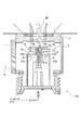
図1は本発明のイオン注入装置の一例を模式的に示す説明図である。図1に示した装置は、アーク放電型のイオン源5、イオン源5に所定ガスを供給するボンベ17及び1対の引出電極8、9を含むイオン引出アセンブリ100、イオン質量セレクタ130、並びにターゲット基板ホルダ140を備えるものである。
【0025】
図2はイオン引出アセンブリ100の概略構成を示す断面図である。同図において、イオン引出アセンブリ100はソースチャンバ3を有し、このソースチャンバ3内はターボポンプ4により所定の真空度に減圧されている。ソースチャンバ3内にはイオン源5が収容されている。
【0026】
このイオン源5はアーク放電型のもので、ガス供給源(図示せず)からプラズマチャンバ内に導入されるドーピングガスを放電させてプラズマ状態を作り出し、所定の元素(分子)をイオン化させるものである。導入されるガスは、質量数20以下のイオンを発生させるためのもので、例えば、水素、ヘリウム又はホウ素のいずれか1種、あるいはこれらの2種以上の混合ガスが好適に使用される。
【0027】
イオン源5の前面には、イオン源5で生成したイオンが出射される2個のスリット10a、10bが、スリット10a、10bの短軸方向に沿って相互に並列となるように形成されている。また、イオン源5の前面側には、イオン源5からイオンを引き出すための引出電極系7が配置されている。この引出電極系7は、図2に示すように、互いに対向配置された1対の引出電極8,9(引出電極8は主電極、引出電極9は接地電極)を有している。
【0028】
主電極8は、2個のスリット12a、12bを有する電極本体12と、この電極本体12を囲むように構成された円盤状の取付プレート13とを有している。また、接地電極9は、スリット14a、14bを有する電極本体14と、この電極本体14を囲むように構成された円盤状の取付プレート15とを有している。スリット主電極8の取付プレート13は、支持部材16aを介してソースチャンバ3に固定されている。また、接地電極9の取付プレート15は、支持部材16bを介してソースチャンバ3に固定されている。
【0029】
主電極8が有するスリット12a、12bはそれらの短軸方向に沿って相互に並列となるように形成されている。同様に、接地電極9が有するスリット14a、14bはそれらの短軸方向に沿って相互に並列となるように形成されている。スリット12a、14aはそれぞれイオン源5のスリット10aに対応して形成されたものであり、スリット12b、14bはそれぞれスリット10bに対応して形成されたものである。
【0030】
イオン源5及び引出電極8、9のそれぞれにおいて、スリット形成領域の短軸方向の幅(例えば、スリット10aのスリット10bから遠い側の長辺と、スリット10bのスリット10aから遠い側の長辺と、の距離)は、質量分析器における所定の分解能(好ましくは50〜100M/ΔM)が得られる幅の範囲内であることが好ましい。
【0031】
このようなイオン引出アセンブリ100において、イオン源5と主電極8との間に所望の電圧を印加すると、スリット10a、10bのそれぞれからイオンが引き出されると共に加速され、イオンビームが形成される。例えば陽イオンを引き出す場合、イオン源5は接地電極9に対して正電圧に、主電極8は接地電極9に対して負電圧に維持される。このときのイオンの引出エネルギーは、下記式(1)で求められる。本発明におけるイオンの引出エネルギーは、好ましくは10keV以下、より好ましくは1keV以下である。
【0032】
E = ZV [eV] = ZeV [J] (1)
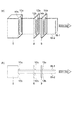
[式(1)中、Eはイオンの引出エネルギーを表し、Zはイオンの電荷数を表し、Vは引出電圧(主電極とイオン源との電位差)を表し、eは電子の電荷を表す。]このようにしてイオンビームが形成されるときのイオン源5及び引出電極8、9の位置関係、並びに各イオンビームの光路を図3に概念的に示す。図3中、(a)は斜視図、(b)は上面図である。図示の通り、スリット10aから引き出されるイオンはイオンビームIB−1を形成し、スリット12a、14aを通ってイオン質量セレクタ130に導かれる。同様に、スリット10bから引き出されるイオンはイオンビームIB−2を形成し、スリット12b、14bを通ってイオン質量セレクタ130に導かれる。
【0033】
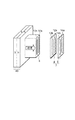
また、ソースチャンバ3内において、イオン源5の周囲には、所定方向に巻回されたソレノイドコイル6が配置されている。ソレノイドコイル6に電流を流すことで、引出電極系7によるイオンの引出方向に沿って磁場が形成される。このときのイオンの引出方向とソレノイドコイル6により形成される磁場の方向との関係を図4に概念的に示す。図示の通り、ソレノイドコイル6の所定の方向に電流を通すと、イオンの引出方向に沿って、すなわちイオン源5のスリット10a(及び10b)から引出電極8、9のスリット12a、14a(及び12b、14b)に向けて磁場が形成され、イオン生成が促進される。このとき、イオン源5から引き出されたイオンの進行方向は実質的にイオンの引出方向(すなわち磁場の方向)のままである。従って、低エネルギーのイオン、あるいはさらに質量数の小さいイオン(例えば水素、ヘリウム又はホウ素等の質量数20以下のイオン)であっても、引き出されたイオンが磁場により曲げられてイオンが引出電極系7等に衝突する現象は起こらず、イオンのビーム電流は高水準に維持される。
【0034】
図1に戻り、イオン引出アセンブリ100からのイオンビームIBは、イオン質量セレクタ130に導入される。
【0035】
イオン質量セレクタ130は、質量選択スリット131と、質量選択スリット131と共に作動する磁気セクタ質量分析器132とを備える。
【0036】
磁気セクタ質量分析器132には、図1の紙面に対して垂直方向の磁場が形成される。また、磁場の調整のために複数方向の磁場が形成される場合もある。そのような磁場の中で、所定の質量/荷電比を持つ定エネルギーのイオンを含むイオンビームが、イオン源5のアークチャンバの出口アパーチャに接近した点を基点とし、分析器132の入口アパーチャから出口アパーチャを通って質量選択スリット131の面で焦点を結ぶ。スリット131は、磁気セクタ質量分析器132からのイオンビームのうち必要とするイオンのみを通過させる。スリット131を通過した所望のイオンはターゲット基板ホルダ140に装着されたターゲット基板141に照射される。スリット131及び磁気セクタ質量分析機132は、ハウジングで囲むか、もしくは機構中にチューブを貫通させる形をとり、その内部はターボポンプ(図示せず)により所定の真空度に減圧されている。
【0037】
図1は、単一の質量/荷電比のイオンビームがスリット131のアパーチャに単一の焦点を結び、ターゲット基板14に向かってスリット131を通過するときの様子を模式的に示しているが、実際には、イオン引出アセンブリ100からのイオンビームには、基板141への注入に望ましいものとは異なる質量/荷電比のイオンも含まれる。これらの望ましくないイオンは、所望のイオンとは異なる曲率半径を持ち、スリットを通過しない。したがって分析器132は、図1の面内に偏向面(ディスパージョンプレーン)を持つ。この偏向面に対して、イオン源5及び引出電極8、9に形成されたスリットの長軸方向は垂直であることが好ましい。
【0038】
このように本実施形態では、イオン源5及び引出電極8、9のそれぞれに、2個のスリットをそれらの短軸方向に沿って相互に並列となるように形成することで、例えばイオン源5及び引出電極8、9のそれぞれにスリットが1個ずつ形成された系(以下、「単一スリット系」という)に比べてイオンの有効引出面積を倍増させることができる。なお、単一スリット系の場合、各スリットのサイズを大きくしてイオンの有効引出面積を増大させると、十分な収束効果が得られずにイオンビームが発散する現象が起こり得るが、上述のようにスリットのサイズは変えずに個数の増加によりイオンの有効引出面積を大きくした場合には、同サイズの単一スリット系の場合と同様の収束効果がイオンビームIB−1、IB−2それぞれについて得られるため、イオンの有効面積の増大によるイオンビームの発散等の現象は起こらず、低エネルギーのイオン、あるいはさらに質量数が小さいイオンを引き出す場合であってもビーム電流を高めることができる。
【0039】
また、このようにして形成されたイオンビームはスリットの形状に対応した良好なビーム形状を有しているため、当該イオンビームをイオン質量セレクタ130に導入することで、イオン注入に必要なイオンを高い分解能で効率よく選択することができる。このようにして選択されたイオンをターゲット141に照射することによって、十分に高いスループットでイオン注入を行うことが可能となる。
【0040】
また、本実施形態においては、イオン源5の周囲を巻回するソレノイドコイル6によりイオンの引出方向に沿って磁場を形成することによって、引き出されたイオンが磁場により曲げられることなくイオン源5からのイオンの引出を促進し、イオンのビーム電流を高水準に維持することができる。このようにアーク放電型のイオン源5の周囲にソレノイドコイル9を配置して上述の磁場を形成することは、イオン源5等の大幅な改良や大型化等を必要とせずにさらなるスループットの向上効果が得られる点で非常に有用である。さらに、上記磁場の形成によるイオンの引出電極への衝突防止に伴い、引出電極等の長寿命化、パーティクル汚染の低減、真空ポンプの長寿命化等の効果も得られる。
【0041】
なお、本発明は上記の実施形態に何ら限定されるものではない。例えば、図3〜6には端部が円弧状である略長方形のスリットを示したが、スリットの形状は長方形であってもよい。
【0042】
また、図1に示したイオン注入装置は、イオン源5及び引出電極8、9にスリットが2個ずつ形成されたものであるが、イオン源及び引出電極のそれぞれが有するスリットの個数は3個以上であってもよい。なお、スリットの個数が3個以上である場合も、スリット形成領域の短軸方向の幅は、質量分析器における所定の分解能(好ましくは50〜100M/ΔM)が得られる幅の範囲内であることが好ましい。さらに、引出電極系7においては、イオン源5のスリットに対応するスリットが主電極8に複数形成されていればよく、接地電極9には主電極8のスリットを通過するイオンビームが衝突しないように1個のスリットを設けてもよい。
【0043】
また、図1に示したイオン注入装置において、イオンの引出方向に沿った磁場の形成手段として、ソレノイドコイル9の代わりに後述する永久磁石又は電磁石を用いることもできる。
【0044】
すなわち、図5に示すように、イオン源5の背面側(引出電極と反対側)に、永久磁石50を引出電極に近い側がN極、引出電極に遠い側がS極となるように配置することによって、イオンの引出方向に沿って磁場が形成されるので、ソレノイドコイル6を用いた場合と同様の効果が得られる。なお、イオンの引出方向に沿って磁場が形成されれば、引出電極に近い側がS極、引出電極に遠い側がN極となるように永久磁石を配置してもよい。
【0045】
また、図6に示すように、イオン源5の背面側(引出電極と反対側)に、軟鋼又は磁性体からなる芯材61と、芯材61の外周を所定の方向に巻回するソレノイドコイル62とを備える電磁石60を配置することによっても、イオンの引出方向に沿って磁場が形成されるので、ソレノイドコイル6を用いた場合と同様の効果を得ることができる。
【0046】
また、本発明では、後述するようにイオン源としてマイクロ波イオン源を用いてもよい。以下、本発明の他の例としてマイクロ波イオン源を用いて水素イオンを注入する場合について説明する。なお、マイクロ波イオン源はホウ素や他の元素を注入する場合にも適用可能である。
【0047】
図7は、図1中のアーク放電型イオン源5と置換可能なマイクロ波イオン源の一例を示す概略構成図である。図7中、マグネトロン21、マグネトロンマウント22、サーキュレータ23、パワーモニタ25、スタブチューナ26、インターフェースチューブ27、ソースヘッド28がこの順で連結されてマイクロ波イオン源が構成されている。ソースヘッド28の前面にはプラズマチャンバ29が設けられている。また、サーキュレータ23の側部にはダミーロード24が設けられている。
【0048】
マグネトロン21は所定のマイクロ波(例えば2.45GHzのもの)を発生させるもので、このマイクロ波がソースヘッド28に導入されてプラズマ生成に利用される。サーキュレータ23はマグネトロン21側に戻ろうとする反射されたマイクロ波をダミーロード24に迂回させるものであり、迂回したマイクロ波はダミーロード24で吸収されて熱に変換される。また、スタブチューナ26はマイクロ波の反射を小さくしてより多くのマイクロ波がプラズマ生成に消費されるように調整するものである。なお、マイクロ波の出力を検出するパワーモニタ25、インターフェースチューブ27等は必須の要素ではなく、適宜省略することができる。
【0049】
図8は、ソースヘッド28をマイクロ波の導入路を含む平面で切断したときの断面図である。図3中、ソースチャンバ31のマグネトロン側(マイクロ波MWの入口側)にはソースブッシング32が形成されており、その端部はソースヘッドの内側に向けて折れ曲がった形状となっている。この折れ曲がり部の先端にはマグネットヨーク33が設けられてソースヘッド28を挿入するための空間を与えている。マグネットヨーク33の前面には開口部を有する出口側プレート34が設けられ、さらにプレート34のマグネトロン側の開口部には凹状のプラズマチャンバ29が配置されている。プラズマチャンバ29の凹部の空間37はプラズマ生成領域であり、この部分に所定ガスが供給される。
【0050】
また、凸状のマグネットポール35は、凸部の先端がプラズマチャンバ29に近接するとともに底部側面がマグネットヨーク33側部の内壁面と密着するように配置されている。このマグネットポール35には底部の中心から凸部先端までを連通するように導波管36が配置されている。この導波管36はマイクロ波をプラズマチャンバ29に導入するものである。
【0051】
マグネットヨーク33及びプレート34の内壁面並びにプラズマチャンバ29及びマグネットポール35の外壁面により形成される空間には、マグネットポール35の凸部を巻回するようにソレノイドコイル38が配置されている。かかる構成により、プラズマチャンバ29から引き出されるイオンの引出方向に沿って磁場が形成される。
【0052】
上記の構成を有するマイクロ波イオン源において、磁場内の電子はローレンツ力を受けて磁束線に沿って旋回する。このとき、プラズマ生成領域37に水素ガスを導入しながら導波管36にマイクロ波を導入すると、磁場内の電子がマイクロ波により励起され、この励起電子とプラズマ生成領域37内のガスとの衝突により水素イオンを含むプラズマが生成する。
【0053】
このようにして生成したイオンを引き出してイオンビームを発生させ、アーク放電型イオン源の場合と同様にイオン質量セレクタ130を介してターゲット基板14にイオンを照射する。なお、図8にはイオン源のスリットは図示していないが、プレート34には2個のスリットが形成されている。これにより、イオンの有効引出面積が増大し、イオンのビーム電流を向上させることができる。また、ソレノイドコイル38によりイオンの引出方向に沿って磁場を形成することで、イオンの進行方向が曲げられて引出電極系7等に衝突する現象を防止でき、低エネルギーのイオン、あるいはさらに質量数の小さいイオンであっても高水準のビーム電流が達成可能となる。
【0054】
本発明において、マイクロ波イオン源を用いたプラズマ生成は、ECRモード、非ECRモード(Off−ECRモード)のいずれで行ってもよいが、水素ガスを用いる場合は非ECRモードで行うことが好ましい。非ECRモードでプラズマ生成を行うことで、低エネルギー電子による水素分子イオンの生成効率及びプラズマ密度を高めることができ、水素イオンビームIBの電流密度及び水素分子イオンの割合を向上させることができる。
【0055】
なお、ここでいうECR(Electron Cyclotron Resonance)モードとは、マイクロ波の周波数を下記式(2):
【0056】
【数1】

[式(2)中、ωeは電子サイクロトロン周波数を表し、meは電子の質量を表し、eは電子の電荷を表し、Bは磁場の強さを表す。]
で表される電子サイクロトロン周波数(磁束線に沿って旋回する電子の周波数)と一致させることによって、電子サイクロトロン共鳴吸収過程で電子を選択的に励起し、その励起電子と水素分子とを衝突させてプラズマを生成させるものである。しかしながら、ECRモードでプラズマ生成を行うと、水素原子イオン(H+)が生成しやすく、水素イオンビームの電流密度が不十分となりやすい。
【0058】
一方、非ECRモードとは、ECR条件を満たさないように、すなわちマイクロ波の周波数及び磁場の強さが下記式(3)又は(4):
【0059】
【数2】
【数3】
[式(3)、(4)中、ωはマイクロ波の周波数を表し、meは電子の質量を表し、eは電子の電荷を表し、Bは磁場の強さを表す]
で表される条件を満たすように設定してプラズマ生成を行うものである。なお、非ECRモード設定の際には、マイクロ波の周波数を固定して磁場の強さを調節してもよく、また、磁場の強さを固定してマイクロ波の周波数を調節してもよい。
【0062】
非ECRモードにおいては、マイクロ波の周波数ωが電子サイクロトロン周波数ωeよりも10〜50%(より好ましくは20〜40%)だけ高く(又は低く)なるように、マイクロ波の周波数及び磁場の強さを設定することが好ましい。従って、例えば2.45GHzのマイクロ波を用いる場合、磁場の強さは96〜131mT又は44〜79mT(より好ましくは105〜123mT又は53〜70mT)であることが好ましい。また、14.5GHzのマイクロ波を用いる場合、磁場の強さは570〜777mT又は259〜466mTであることが好ましい。
【0063】
また、プラズマ生成領域37に水素ガスが導入されてから水素イオンビームIBが引き出されるまでの水素分子の平均滞留時間は、5×10⁻⁴〜5×10⁻³秒であることが好ましく、7×10⁻⁴〜3×10⁻³秒であることがより好ましい。平均滞留時間が前記上限値を超えると水素分子イオンの割合が低下する傾向にあり、また、前記下限値未満であるとプラズマの生成効率が低下する傾向にある。当該平均滞留時間の設定は、プラズマチャンバ29の形状及びサイズ、水素ガスの供給量、水素イオンビームIBの引き出し量等の調節により行うことができる。
【0064】
なお、アーク放電型イオン源やRFイオン源等を用いた従来法では、水素分子イオンよりも水素原子イオンの方が生成しやすいため、イオン注入の際には専ら水素原子イオンが利用されていた。これに対して本発明のイオン注入方法では、マイクロ波を利用してプラズマ生成を行い、イオンの引出方向に沿って磁場を形成してイオンを引き出すことで、従来法に比べてプラズマ中の水素分子イオンの割合を飛躍的に増大させ、さらにはその水素分子イオンを低い引出エネルギーで且つ高いビーム電流で利用することができる。従って、従来では達成が困難であった高水準のスループットを容易に実現することができる。
【0065】
例えば、本発明者は、マイクロ波の周波数が2.45GHz、マイクロ波の出力が700W、磁場の強さが70mTである非ECRモードにおいて、水素分子の平均滞留時間を8.9×10⁻⁴秒としてプラズマを生成させたとき、H+イオンが13.5%、H2 +イオンが78.1%、H3 +イオンが8.4%というイオン組成が達成されたことを確認している。これに対して、従来型のアーク放電型イオン源により生成したプラズマ中のイオン組成は、H+イオンが60.2%、H2 +イオンが22.9%、H3 +イオンが16.9%であった。
【0066】
本発明のイオン注入装置及びイオン注入方法は、上述のように高水準のスループットの達成が可能なものであり、高ドーズのイオン注入を要するトランジスターの接合部形成やSOIウェハのイオン注入層形成等の工程において非常に有用である。
【0067】
ここで、SOIウェハの製造方法について、Si層/SiO2層/Si基板の積層構造を有するSOIウェハを製造する場合を例にとって詳述する。
【0068】
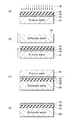
図9(a)〜(d)はそれぞれ各工程におけるウエハの積層構造を模式的に示す断面図である。
【0069】
イオン注入工程においては、ターゲット基板として、Si基板(Si−donor wafer)91の一方面上にSiO2層92が形成されたものを用いる。SiO2層92は、例えばSi基板の表面を酸化させることにより形成可能であり、その厚さは例えば0.01〜1.0μmである。
【0070】
このターゲット基板に対して、ウェハのSiO2層92側から水素分子イオンを照射することによって、Si基板92中の所定深さに水素イオン注入層93が形成され、これに伴いSiO2層92と水素イオン注入層93との間に薄いSi層が形成される(図9(a))。
【0071】
イオン注入工程において、マイクロ波イオン源を用いる場合は、非ECRモードによるプラズマ生成を行うことが好ましい。これにより、水素分子イオンの生成が促進されるため、非常に高いスループットが実現可能となり、その結果、SOIウェハの製造効率を飛躍的に向上させることができる。
【0072】
イオン注入工程におけるイオン注入量は1×10¹⁶ions/cm2以上であることが好ましい。また、水素イオン注入層93は、例えばSi層94とSiO2層82との界面からの深さ0.005〜1.5μmの位置に形成される。
【0073】
次に、ターゲット基板のSiO2層92上にSi基板(Si−handle wafer)95を貼り合わせる(図9(b))。なお、SiO2層が形成されていないSi基板を用いて上記と同様のイオン注入工程を行い、その一方で表面にSiO2層が形成されたSi基板を用意して、積層工程において両者を貼り合わせることによっても目的の積層体を得ることができる。
【0074】
この積層体を水素イオン注入層93で分断する(図9(c))。水素イオン注入層93はシリコン原子同士の共有結合が切断された脆弱な層であるため、水素イオン注入層93の側面に乾燥空気等のガスを吹き付けたり、機械的に剪断を加えたりすることによって容易に分断することができる。
【0075】
このようにして、Si基板95上にSiO2層92及びSi層94がこの順で積層されたSOIウェハが得られる(図9(c))。なお、分断工程後のSi層94の表面に水素イオン注入層93の一部が残存する場合があるが、研磨処理等を行うことでその残さを容易に除去することができる。また、Si層94を更に研磨することにより、Si層94の厚みを調整することができる。
【0076】
【発明の効果】
以上説明した通り、本発明のイオン注入装置及びイオン注入方法によれば、イオン源中のプラズマ密度をほとんど変化させずに、また、引出電極によるイオンビームの収束効果を損なわずに、イオンの有効引出面積を増大させることができるので、低エネルギーのイオンを引き出す場合であってもビーム電流が高められ、高水準のスループットが実現可能となる。
【0077】
また、本発明のSOIウェハの製造方法によれば、イオン注入工程の際に上記本発明のイオン注入方法を適用することで高水準のスループットが実現可能となり、高集積化等の点で優れたSOIウェハを効率よく且つ確実に製造することができる。
【図面の簡単な説明】
【図1】本発明のイオン注入装置の一例を示す概略構成図である。
【図2】図1に示したイオン注入装置が備えるイオン引出アセンブリ100の概略構成を示す断面図である。
【図3】(a)、(b)はそれぞれイオンビームが形成されるときのイオン源及び引出電極の位置関係、並びに各イオンビームの光路を示す概念図であり、(a)は斜視図、(b)は上面図である。
【図4】ソレノイドコイルにより形成される磁場の方向とイオンの引出方向との関係を示す概念図である。
【図5】永久磁石により形成される磁場の方向とイオンの引出方向との関係を示す概念図である。
【図6】電磁石により形成される磁場の方向とイオンの引出方向との関係を示す概念図である。
【図7】マイクロ波イオン源の一例を示す概略構成図である。
【図8】図7に示したマイクロ波イオン源のソースヘッドをマイクロ波の導入路を含む平面で切断したときの断面図である。
【図9】(a)〜(d)はそれぞれ各工程におけるウエハの積層構造を模式的に示す断面図である。
【符号の説明】
100…イオン引出アセンブリ、130…イオン質量セレクタ、131…質量選択スリット、132…磁気セクタ質量分析器、140…ターゲット基板、141…ターゲット基板ホルダ、3…ソースチャンバ、4…ターボポンプ、5…イオン源、6…ソレノイドコイル、7…引出電極系、8…主電極、9…接地電極、12、14…電極本体、10a、10b、12a、12b、14a、14b…スリット、15…取付プレート、17…ボンベ、21…マグネトロン、22…マグネトロンマウント、23…サーキュレータ、24…ダミーロード、25…パワーモニタ、26…スタブチューナ、27…インターフェースチューブ、28…ソースヘッド、29…プラズマチャンバ、31…ソースチャンバ、32…ソースブッシング、33…マグネットヨーク、34…出口側プレート、35…マグネットポール、36…導波管、37…プラズマ生成領域、38…ソレノイドコイル、50…永久磁石、60…電磁石、61…心材、62…ソレノイドコイル、91、95…Si基板、92…SiO2層、93…水素イオン注入層、94…Si層、IB…イオンビーム、MW…マイクロ波。[0001]
TECHNICAL FIELD OF THE INVENTION
The present invention relates to an ion implantation apparatus and method.
[0002]
[Prior art]
Conventionally, an ion implantation process has been used as a method of embedding a dopant in an IC device.
[0003]
In addition, the ion implantation process is also used in the smart cut method, which is one of the methods for manufacturing an SOI wafer (Silicon @ on @ Insulator). The smart cut method refers to an insulating layer (SiO 2) formed on the surface of a Si substrate.2In this method, an SOI wafer is manufactured by implanting hydrogen ions into a Si substrate through a layer or the like, bonding the substrate to another Si substrate, and then dividing the substrate at a hydrogen ion implanted layer.
[0004]
As an ion implantation apparatus used for this ion implantation process, there is known an ion implantation apparatus provided with an ion source for generating plasma containing predetermined ions in a plasma chamber by arc discharge or microwave excitation (for example, Patent Document 1).
[0005]
[Patent Document 1]
JP-A-9-283074
[0006]
[Problems to be solved by the invention]
By the way, with the recent miniaturization and high performance of IC devices, the energy of implanted ions is decreasing at an accelerating rate. For example, when boron (B) is implanted, it is required that the energy of ions be less than 1 keV.
[0007]
However, in the case of the above-described conventional ion implantation apparatus, when trying to implant low-energy ions, the beam current of the ions decreases. Therefore, in a process such as formation of a junction of a transistor which requires high dose ion implantation or formation of an ion implantation layer of an SOI wafer, ion implantation cannot be performed with a reasonable throughput.
[0008]
The present invention has been made in view of the above-mentioned problems of the related art, and when performing low-energy ion implantation, an ion implantation apparatus capable of maintaining a current amount of an ion beam at a high level and achieving a sufficient throughput. And a method, and a method for manufacturing an SOI wafer.
[0009]
[Means for Solving the Problems]
In order to solve the above problems, the ion implantation apparatus of the present invention is an ion source that excites a predetermined gas to generate plasma containing predetermined ions, and an extraction electrode that extracts ions from the ion source to generate an ion beam, A mass analyzer that introduces an ion beam into a predetermined magnetic field and selects ions to be implanted into the semiconductor substrate from the ion beam.In the ion implantation apparatus, the ion source has a plurality of slits from which ions are extracted. The slits are formed so as to be parallel to each other along the short axis direction, and a plurality of slits corresponding to each slit of the ion source are formed in the extraction electrode so as to be parallel to each other. .
[0010]
Thus, the plurality of slits are formed in the ion source so as to be parallel to each other along the short axis direction, and the plurality of slits corresponding to each slit of the ion source are formed in the extraction electrode so as to be parallel to each other. The effective extraction area of the ions can be increased without substantially changing the plasma density in the ion source and without impairing the convergence effect (optical lens effect) of the ion beam by the extraction electrode. Therefore, even when extracting low-energy ions, the beam current can be increased. Further, the ion beam generated in this manner has a good beam shape corresponding to the shape of the slit (rectangular or substantially rectangular with rounded corners), so that the desired ion is It can be effectively selected from ion beams. Therefore, in the process of forming a junction of a transistor requiring high dose ion implantation or forming an ion implantation layer of an SOI wafer by the ion implantation device of the present invention, a high level of ion implantation which has been difficult to achieve with the conventional ion implantation device is used. Throughput becomes feasible.
[0011]
According to the study of the present inventor, in a conventional ion implantation apparatus in which one slit is formed in the ion source and the extraction electrode, the size of the ion beam extracted from the ion source is simply increased by increasing the size of the slit itself. It is possible to increase the amount of current. However, in such a method, the convergence effect (optical lens effect) of the ions by the extraction electrode is reduced, the ion beam diverges, and the current amount of the beam that can reach the wafer is reduced. It is very difficult to get.
[0012]
Further, as means for increasing the effective extraction area of ions, shower-like ions may be extracted by forming a plurality of circular holes in the ion source and the extraction electrode instead of the plurality of slits according to the present invention. In this case, the total width of the ion beam becomes large. Even if an attempt is made to select desired ions from such an ion beam, a sufficient resolution (for example, 50 to 100 M / ΔM) cannot be obtained in the mass analyzer, and the above-described effect of improving the throughput cannot be achieved.
[0013]
The ion implantation apparatus of the present invention may be characterized in that the major axes of the plurality of slits of the ion source and the extraction electrode are perpendicular to the deflection surface of the mass analyzer. Thus, a desired ion can be efficiently selected from the ion beam with high resolution in the mass analyzer.
[0014]
Further, the ion implantation apparatus of the present invention may be characterized in that the extraction electrode includes a main electrode and a ground electrode which are arranged to face each other, and a plurality of slits are formed in the main electrode.
[0015]
Further, the ion implantation apparatus of the present invention may be characterized in that the extraction electrode extracts ions at an extraction energy of 10 keV or less. According to the ion implantation apparatus of the present invention, a high level of throughput can be achieved even when such low energy ions are extracted.
[0016]
In addition, the ion implantation apparatus of the present invention may further include a magnet that forms a magnetic field along a direction in which ions are extracted. By forming a magnetic field along the direction in which ions are extracted, ion generation can be promoted. Further, since the magnetic field does not affect the traveling direction of the extracted ions, the traveling direction of the ions is substantially the same as the extraction direction of the ions (that is, the direction of the magnetic field), and the extracted ions are bent by the magnetic field. The phenomenon in which the ions collide with the extraction electrode or the like does not occur. Therefore, even if the ions are low energy ions or ions having a smaller mass number, the extracted ions are subjected to ion implantation while the beam current is maintained at a high level, so that the throughput can be further increased. .
[0017]
In addition, the ion implantation method of the present invention includes the steps of: exciting a predetermined gas in an ion source to generate plasma containing predetermined ions; extracting ions from the ion source by an extraction electrode to generate an ion beam; Selecting an ion to be implanted into the semiconductor substrate from the ion beam by introducing an ion beam to a predetermined magnetic field in a vessel, wherein a plurality of slits are provided along the minor axis direction of the slit as an ion source. A plurality of slits corresponding to the respective slits of the ion source were used as extraction electrodes, each of which was formed so as to be parallel to each other. The ion beam generated from each slit passes through the slit corresponding to each slit of the ion source formed on the extraction electrode. And introducing into the mass spectrometer. As a result, the beam current can be increased even when extracting low-energy ions, and the ion beam introduced into the mass spectrometer can be maintained in a good shape. A high level of throughput can be achieved in processes such as formation of a portion and formation of an ion implantation layer of an SOI wafer.
[0018]
The ion implantation method of the present invention may be characterized in that ions are extracted by an extraction electrode at an extraction energy of 10 keV or less.
[0019]
Further, the ion implantation method of the present invention may be characterized in that a magnetic field is formed along the extraction direction of the ions. By forming such a magnetic field, the throughput can be further increased.
[0020]
Further, the method for manufacturing an SOI wafer according to the present invention includes an ion implantation step of forming a hydrogen ion implantation layer at a predetermined depth of a first wafer having an insulating layer on one surface of a Si substrate, and a second step after the ion implantation step. A method for manufacturing an SOI wafer, comprising: a laminating step of laminating a second wafer made of a Si substrate on an insulating layer of one wafer to obtain a laminated body; and a dividing step of dividing the laminated body by the hydrogen ion implanted layer. In the ion implantation step, a hydrogen ion implantation layer is formed by the above-described ion implantation method of the present invention.
[0021]
In the above manufacturing method, a hydrogen ion implanted layer is formed at a predetermined depth of a first wafer (insulating layer / Si substrate), and a second wafer is stacked on the insulating layer to form a laminate (Si substrate / insulating layer). / Si layer / hydrogen ion implanted layer / Si substrate), and this laminate is divided by the hydrogen ion implanted layer to obtain an SOI wafer (Si layer / insulating layer / Si substrate). At this time, by applying the above-described ion implantation method of the present invention in the ion implantation step, hydrogen ions can be efficiently implanted to a predetermined depth of the Si substrate, thereby dramatically improving the throughput. Therefore, the above manufacturing method is very useful in that an SOI wafer excellent in high integration and the like can be efficiently and reliably manufactured.
[0022]
BEST MODE FOR CARRYING OUT THE INVENTION
Hereinafter, preferred embodiments of the present invention will be described with reference to the drawings. In the drawings, the same or corresponding portions will be denoted by the same reference characters, without redundant description.
[0023]
First, an ion implantation method and an ion implantation apparatus will be described.
[0024]
FIG. 1 is an explanatory view schematically showing one example of the ion implantation apparatus of the present invention. The apparatus shown in FIG. 1 includes an
[0025]
FIG. 2 is a sectional view showing a schematic configuration of the
[0026]
The
[0027]
On the front surface of the
[0028]
The
[0029]
The
[0030]
In each of the
[0031]
In the
[0032]
E = {ZV [eV] = {ZeV [J] (1)
[In the formula (1), E represents the extraction energy of the ions, Z represents the number of charges of the ions, V represents the extraction voltage (the potential difference between the main electrode and the ion source), and e represents the charges of the electrons. FIG. 3 conceptually shows the positional relationship between the
[0033]
A
[0034]
Returning to FIG. 1, the ion beam IB from the
[0035]
The
[0036]
In the magnetic
[0037]
FIG. 1 schematically shows a state in which an ion beam having a single mass / charge ratio has a single focus on the aperture of the
[0038]
As described above, in the present embodiment, two slits are formed in each of the
[0039]
In addition, since the ion beam formed in this manner has a good beam shape corresponding to the shape of the slit, the ion beam required for ion implantation is introduced by introducing the ion beam into the
[0040]
Further, in the present embodiment, the magnetic field is formed along the direction in which the ions are extracted by the
[0041]
Note that the present invention is not limited to the above embodiment. For example, FIGS. 3 to 6 show a substantially rectangular slit having an arc-shaped end, but the slit may have a rectangular shape.
[0042]
The ion implantation apparatus shown in FIG. 1 has two slits formed in each of the
[0043]
Further, in the ion implantation apparatus shown in FIG. 1, a permanent magnet or an electromagnet, which will be described later, can be used instead of the
[0044]
That is, as shown in FIG. 5, the
[0045]
As shown in FIG. 6, a core material 61 made of mild steel or a magnetic material, and a solenoid coil wound around the outer periphery of the core material 61 in a predetermined direction, on the back side of the ion source 5 (the side opposite to the extraction electrode). Also, by arranging the electromagnet 60 provided with 62, a magnetic field is formed along the direction in which ions are extracted, so that the same effect as when the
[0046]
In the present invention, a microwave ion source may be used as the ion source as described later. Hereinafter, a case where hydrogen ions are implanted using a microwave ion source will be described as another example of the present invention. Note that the microwave ion source is also applicable to a case where boron or another element is implanted.
[0047]
FIG. 7 is a schematic configuration diagram showing an example of a microwave ion source that can be replaced with the arc
[0048]
The
[0049]
FIG. 8 is a cross-sectional view when the
[0050]
The
[0051]
In a space formed by the inner wall surfaces of the
[0052]
In the microwave ion source having the above configuration, the electrons in the magnetic field rotate along the magnetic flux lines under Lorentz force. At this time, when microwaves are introduced into the
[0053]
The ions thus generated are extracted to generate an ion beam, and the
[0054]
In the present invention, plasma generation using a microwave ion source may be performed in any of an ECR mode and a non-ECR mode (Off-ECR mode). However, when a hydrogen gas is used, it is preferably performed in a non-ECR mode. . By performing plasma generation in the non-ECR mode, it is possible to increase the efficiency of generation of hydrogen molecule ions by low-energy electrons and the plasma density, and to improve the current density of the hydrogen ion beam IB and the ratio of hydrogen molecule ions.
[0055]
Note that the ECR (Electron @ Cyclotron @ Resonance) mode here means that the frequency of the microwave is calculated by the following equation (2):
[0056]
(Equation 1)
[In equation (2), ωeRepresents the electron cyclotron frequency and meRepresents the mass of the electron, e represents the charge of the electron, and B represents the strength of the magnetic field. ]
By selectively matching the electron cyclotron frequency (frequency of the electron orbiting along the magnetic flux lines) with the electron cyclotron resonance absorption process, the excited electrons collide with hydrogen molecules. This is to generate plasma. However, when plasma is generated in the ECR mode, hydrogen atom ions (H+) Is easily generated, and the current density of the hydrogen ion beam tends to be insufficient.
[0058]
On the other hand, the non-ECR mode means that the ECR condition is not satisfied, that is, the frequency of the microwave and the strength of the magnetic field are expressed by the following formula (3) or (4):
[0059]
(Equation 2)
(Equation 3)
[In the formulas (3) and (4), ω represents the frequency of the microwave, and meRepresents the mass of the electron, e represents the charge of the electron, and B represents the strength of the magnetic field.
The plasma generation is performed by setting so as to satisfy the condition represented by. In setting the non-ECR mode, the strength of the magnetic field may be adjusted by fixing the frequency of the microwave, or the frequency of the microwave may be adjusted by fixing the strength of the magnetic field. .
[0062]
In the non-ECR mode, the microwave frequency ω is equal to the electron cyclotron frequency ωeIt is preferable to set the frequency of the microwave and the strength of the magnetic field so as to be higher (or lower) by 10 to 50% (more preferably 20 to 40%). Therefore, for example, when a microwave of 2.45 GHz is used, the strength of the magnetic field is preferably 96 to 131 mT or 44 to 79 mT (more preferably 105 to 123 mT or 53 to 70 mT). When a microwave of 14.5 GHz is used, the strength of the magnetic field is preferably 570 to 777 mT or 259 to 466 mT.
[0063]
The average residence time of hydrogen molecules from the introduction of hydrogen gas into the
[0064]
In the conventional method using an arc discharge type ion source, an RF ion source, and the like, hydrogen atom ions are more easily generated than hydrogen molecule ions, and thus hydrogen ion ions are exclusively used for ion implantation. . On the other hand, in the ion implantation method of the present invention, plasma is generated using microwaves, and a magnetic field is formed along the extraction direction of the ions to extract the ions. The ratio of molecular ions can be greatly increased, and the hydrogen molecular ions can be used with low extraction energy and high beam current. Therefore, it is possible to easily realize a high level of throughput which has been difficult to achieve in the past.
[0065]
For example, in the non-ECR mode in which the microwave frequency is 2.45 GHz, the microwave output is 700 W, and the magnetic field strength is 70 mT, the inventor has set the average residence time of hydrogen molecules at 8.9 × 10 4-4When a plasma is generated in seconds, H+13.5% ion, H2 +78.1% ion, H3 +It has been confirmed that an ion composition of 8.4% of ions was achieved. On the other hand, the ion composition in the plasma generated by the conventional arc discharge ion source is H+60.2% ion, H2 +22.9% ion, H3 +The ion was 16.9%.
[0066]
The ion implantation apparatus and the ion implantation method of the present invention are capable of achieving a high level of throughput as described above, such as formation of a junction portion of a transistor requiring high dose ion implantation and formation of an ion implantation layer of an SOI wafer. It is very useful in the step.
[0067]
Here, regarding the manufacturing method of the SOI wafer, the Si layer / SiO2The case of manufacturing an SOI wafer having a layered structure of a layer / Si substrate will be described in detail as an example.
[0068]
FIGS. 9A to 9D are cross-sectional views schematically showing the laminated structure of the wafer in each step.
[0069]
In the ion implantation step, as a target substrate, a Si substrate (Si-donor wafer)2The one on which the
[0070]
For this target substrate, the SiO2By irradiating hydrogen molecular ions from the
[0071]
When a microwave ion source is used in the ion implantation step, it is preferable to perform plasma generation in a non-ECR mode. Thereby, the generation of hydrogen molecular ions is promoted, so that a very high throughput can be realized, and as a result, the manufacturing efficiency of the SOI wafer can be drastically improved.
[0072]
The ion implantation amount in the ion implantation step is 1 × 10¹⁶ions / cm2It is preferable that it is above. The hydrogen ion implanted
[0073]
Next, the target substrate SiO2A Si substrate (Si-handle @ wafer) 95 is bonded onto the layer 92 (FIG. 9B). In addition, SiO2An ion implantation step similar to the above is performed using a Si substrate on which no layer is formed, while a SiO 22A target laminated body can also be obtained by preparing an Si substrate on which layers are formed and bonding them together in a laminating step.
[0074]
This stacked body is divided by the hydrogen ion implanted layer 93 (FIG. 9C). Since the hydrogen ion implanted
[0075]
Thus, the
[0076]
【The invention's effect】
As described above, according to the ion implantation apparatus and the ion implantation method of the present invention, the effective ion implantation can be performed without substantially changing the plasma density in the ion source and without impairing the convergence effect of the ion beam by the extraction electrode. Since the extraction area can be increased, the beam current can be increased even when extracting low energy ions, and a high level of throughput can be realized.
[0077]
Further, according to the method for manufacturing an SOI wafer of the present invention, a high level of throughput can be realized by applying the above-described ion implantation method of the present invention at the time of the ion implantation step, which is excellent in terms of high integration and the like. SOI wafers can be manufactured efficiently and reliably.
[Brief description of the drawings]
FIG. 1 is a schematic configuration diagram showing one example of an ion implantation apparatus of the present invention.
FIG. 2 is a sectional view showing a schematic configuration of an
3A and 3B are conceptual diagrams showing a positional relationship between an ion source and an extraction electrode when an ion beam is formed, and an optical path of each ion beam, respectively. FIG. (B) is a top view.
FIG. 4 is a conceptual diagram showing the relationship between the direction of a magnetic field formed by a solenoid coil and the direction in which ions are extracted.
FIG. 5 is a conceptual diagram showing the relationship between the direction of a magnetic field formed by a permanent magnet and the direction in which ions are extracted.
FIG. 6 is a conceptual diagram showing the relationship between the direction of a magnetic field formed by an electromagnet and the direction in which ions are extracted.
FIG. 7 is a schematic configuration diagram illustrating an example of a microwave ion source.
8 is a cross-sectional view when the source head of the microwave ion source shown in FIG. 7 is cut along a plane including a microwave introduction path.
9 (a) to 9 (d) are cross-sectional views schematically showing a laminated structure of a wafer in each step.
[Explanation of symbols]
Claims (9)
前記イオン源には前記イオンが引き出される複数のスリットが該スリットの短軸方向に沿って相互に並列となるように形成されており、前記引出電極には前記イオン源の各スリットに対応する複数のスリットが該スリットの短軸方向に沿って相互に並列となるように形成されていることを特徴とするイオン注入装置。An ion source that excites a predetermined gas to generate a plasma containing predetermined ions, an extraction electrode that extracts the ions from the ion source to generate an ion beam, and introduces the ion beam into a predetermined magnetic field to generate an ion beam. A mass analyzer for selecting ions to be implanted into the semiconductor substrate;
A plurality of slits from which the ions are extracted are formed in the ion source so as to be parallel to each other along a short axis direction of the slit, and a plurality of slits corresponding to each slit of the ion source are formed in the extraction electrode. Wherein the slits are formed so as to be parallel to each other along the minor axis direction of the slits.
前記イオン源として複数のスリットが該スリットの短軸方向に沿って相互に並列となるように形成されたものを、前記引出電極として前記イオン源の各スリットに対応する複数のスリットが相互に並列となるように形成されたものをそれぞれ用い、
前記イオン源に形成された各スリットから発生するイオンビームを、前記引出電極に形成された前記イオン源の各スリットに対応するスリットを通して前記質量分析器に導入することを特徴とするイオン注入方法。Generating a plasma containing predetermined ions by exciting a predetermined gas in the ion source; generating ions by extracting ions from the ion source with an extraction electrode; and converting the ion beam to a predetermined magnetic field in a mass analyzer. Selecting an ion to be implanted into the semiconductor substrate from the ion beam by introducing the ion implantation method,
A plurality of slits as the ion source are formed so as to be parallel to each other along the short axis direction of the slit, and a plurality of slits corresponding to each slit of the ion source are parallel to each other as the extraction electrode. Using each formed so that
An ion implantation method, wherein an ion beam generated from each slit formed in the ion source is introduced into the mass analyzer through a slit corresponding to each slit of the ion source formed in the extraction electrode.
前記イオン注入工程において、請求項6〜8のうちのいずれか一項に記載のイオン注入方法により前記水素イオン注入層を形成することを特徴とするSOIウェハの製造方法。An ion implantation step of forming a hydrogen ion implantation layer at a predetermined depth of a first wafer having an insulating layer on one surface of a Si substrate; and a step of forming a hydrogen ion implantation layer on the first wafer after the ion implantation step. A method for manufacturing an SOI wafer, comprising: a laminating step of laminating a second wafer made of a substrate to obtain a laminated body; and a dividing step of dividing the laminated body by the hydrogen ion implantation layer.
A method for manufacturing an SOI wafer, comprising forming the hydrogen ion-implanted layer by the ion implantation method according to claim 6 in the ion implantation step.
Priority Applications (1)
| Application Number | Priority Date | Filing Date | Title |
|---|---|---|---|
| JP2002305975A JP2004139944A (en) | 2002-10-21 | 2002-10-21 | Ion implantation device and ion implantation method |
Applications Claiming Priority (1)
| Application Number | Priority Date | Filing Date | Title |
|---|---|---|---|
| JP2002305975A JP2004139944A (en) | 2002-10-21 | 2002-10-21 | Ion implantation device and ion implantation method |
Publications (1)
| Publication Number | Publication Date |
|---|---|
| JP2004139944A true JP2004139944A (en) | 2004-05-13 |
Family
ID=32452914
Family Applications (1)
| Application Number | Title | Priority Date | Filing Date |
|---|---|---|---|
| JP2002305975A Pending JP2004139944A (en) | 2002-10-21 | 2002-10-21 | Ion implantation device and ion implantation method |
Country Status (1)
| Country | Link |
|---|---|
| JP (1) | JP2004139944A (en) |
Cited By (7)
| Publication number | Priority date | Publication date | Assignee | Title |
|---|---|---|---|---|
| JP2009135468A (en) * | 2007-11-01 | 2009-06-18 | Semiconductor Energy Lab Co Ltd | Semiconductor substrate and method for manufacturing the same, and method for manufacturing semiconductor device |
| US8772128B2 (en) | 2007-10-10 | 2014-07-08 | Semiconductor Energy Laboratory Co., Ltd. | Method for manufacturing semiconductor device |
| JP2015532507A (en) * | 2012-09-28 | 2015-11-09 | メビオン・メディカル・システムズ・インコーポレーテッド | Control of particle beam intensity |
| US9681531B2 (en) | 2012-09-28 | 2017-06-13 | Mevion Medical Systems, Inc. | Control system for a particle accelerator |
| WO2017134817A1 (en) * | 2016-02-05 | 2017-08-10 | 株式会社日立ハイテクノロジーズ | Gas field ionization source, ion beam device, and beam irradiation method |
| USRE48047E1 (en) | 2004-07-21 | 2020-06-09 | Mevion Medical Systems, Inc. | Programmable radio frequency waveform generator for a synchrocyclotron |
| US11017974B2 (en) | 2016-11-11 | 2021-05-25 | Nissin Ion Equipment Co., Ltd. | Ion source |
-
2002
- 2002-10-21 JP JP2002305975A patent/JP2004139944A/en active Pending
Cited By (10)
| Publication number | Priority date | Publication date | Assignee | Title |
|---|---|---|---|---|
| USRE48047E1 (en) | 2004-07-21 | 2020-06-09 | Mevion Medical Systems, Inc. | Programmable radio frequency waveform generator for a synchrocyclotron |
| US8772128B2 (en) | 2007-10-10 | 2014-07-08 | Semiconductor Energy Laboratory Co., Ltd. | Method for manufacturing semiconductor device |
| TWI450337B (en) * | 2007-10-10 | 2014-08-21 | Semiconductor Energy Lab | Method for manufacturing semiconductor device |
| JP2009135468A (en) * | 2007-11-01 | 2009-06-18 | Semiconductor Energy Lab Co Ltd | Semiconductor substrate and method for manufacturing the same, and method for manufacturing semiconductor device |
| JP2015532507A (en) * | 2012-09-28 | 2015-11-09 | メビオン・メディカル・システムズ・インコーポレーテッド | Control of particle beam intensity |
| US9681531B2 (en) | 2012-09-28 | 2017-06-13 | Mevion Medical Systems, Inc. | Control system for a particle accelerator |
| US9723705B2 (en) | 2012-09-28 | 2017-08-01 | Mevion Medical Systems, Inc. | Controlling intensity of a particle beam |
| JP2018110133A (en) * | 2012-09-28 | 2018-07-12 | メビオン・メディカル・システムズ・インコーポレーテッド | Intensity controller of particle beam |
| WO2017134817A1 (en) * | 2016-02-05 | 2017-08-10 | 株式会社日立ハイテクノロジーズ | Gas field ionization source, ion beam device, and beam irradiation method |
| US11017974B2 (en) | 2016-11-11 | 2021-05-25 | Nissin Ion Equipment Co., Ltd. | Ion source |
Similar Documents
| Publication | Publication Date | Title |
|---|---|---|
| JP4328067B2 (en) | Ion implantation method, SOI wafer manufacturing method, and ion implantation apparatus | |
| JP4289837B2 (en) | Ion implantation method and method for manufacturing SOI wafer | |
| JP5057196B2 (en) | Mass spectrometer, ion implanter, and ion beam containment method | |
| US5206516A (en) | Low energy, steered ion beam deposition system having high current at low pressure | |
| JP2903118B2 (en) | Electron cyclotron resonance ion source | |
| TWI354308B (en) | Method and system for ion beam containment in an i | |
| JP4793696B2 (en) | Method and apparatus for selective pre-dispersion of an extracted ion beam in an ion implantation system | |
| JP2001043825A (en) | Ion implantation device and ion implantation | |
| JP2010541164A (en) | Single wafer ion implanter for manufacturing silicon-on-insulator wafers | |
| US6541781B1 (en) | Waveguide for microwave excitation of plasma in an ion beam guide | |
| TW497159B (en) | System and method for removing contaminant particles relative to an ion beam | |
| US8760054B2 (en) | Microwave plasma electron flood | |
| WO2005117059A1 (en) | Charge neutralization device | |
| JP2004139944A (en) | Ion implantation device and ion implantation method | |
| JP3387488B2 (en) | Ion beam irradiation equipment | |
| JP3265227B2 (en) | Doping apparatus and doping method | |
| JP2002056786A (en) | Ion source for ion implanting equipment | |
| JP2000012293A (en) | Neutral beam generating device | |
| US7812320B2 (en) | Ion source element, ion implanter having the same and method of modifying the same | |
| JP3168776B2 (en) | High-frequency charged particle accelerator | |
| TWI835836B (en) | Scanning magnet design with enhanced efficiency | |
| JP2004152690A (en) | Ion implanting device and method, and manufacturing method of soi wafer | |
| Tokiguchi et al. | High-current microwave ion source for wide-energy-range O+ ion implantation | |
| JP3341497B2 (en) | High frequency type charged particle accelerator | |
| JPH09245995A (en) | Charged particle removing mechanism using a plurality of electrodes of radical source |
Legal Events
| Date | Code | Title | Description |
|---|---|---|---|
| A977 | Report on retrieval |
Free format text: JAPANESE INTERMEDIATE CODE: A971007 Effective date: 20050930 |
|
| A131 | Notification of reasons for refusal |
Free format text: JAPANESE INTERMEDIATE CODE: A131 Effective date: 20051101 |
|
| A02 | Decision of refusal |
Free format text: JAPANESE INTERMEDIATE CODE: A02 Effective date: 20060328 |