JP2004111865A - Semiconductor substrate and its fabricating process - Google Patents
Semiconductor substrate and its fabricating process Download PDFInfo
- Publication number
- JP2004111865A JP2004111865A JP2002275882A JP2002275882A JP2004111865A JP 2004111865 A JP2004111865 A JP 2004111865A JP 2002275882 A JP2002275882 A JP 2002275882A JP 2002275882 A JP2002275882 A JP 2002275882A JP 2004111865 A JP2004111865 A JP 2004111865A
- Authority
- JP
- Japan
- Prior art keywords
- buffer layer
- gan
- temperature
- substrate
- semiconductor substrate
- Prior art date
- Legal status (The legal status is an assumption and is not a legal conclusion. Google has not performed a legal analysis and makes no representation as to the accuracy of the status listed.)
- Pending
Links
Images


Landscapes
- Crystals, And After-Treatments Of Crystals (AREA)
- Semiconductor Lasers (AREA)
- Led Devices (AREA)
Abstract
Description
【0001】
【発明の属する技術分野】
本発明は、半導体基板及びその製造方法に関し、詳しくは、半導体レーザ素子や青色レーザダイオード等の発光素子を形成するのに好適なエピタキシャルウェハ等の半導体基板及びその製造方法に関する。
【0002】
【従来の技術】
近年、カラーディスプレイや光デイスク用途として青色LEDやレーザのニーズが高まっており、かかる青色或いは紫外領域の波長光を放出する材料としてGaN系材料が脚光を浴びている。このようなGaN系のエピタキシャル膜を形成する基板としては、形成すべきエピタキシャル膜と格子整合するGaN基板を用いることが望ましいが、このようなGaN基板の製作は非常に困難である。そこで、一般には、格子定数がGaN系エピタキシャル膜と比較的近いサファイヤ基板が用いられている。また、この格子のずれを緩和するために、通常、低温成長されたGaN又はAlNから成るバッファ層が用いられている。
【0003】
また、従来のGaN系エピタキシャル結晶については、単一(シングル)の低温バッファ層が形成され格子ずれによる転位の抑制が図られており、その低温GaNバッファ層の効果についての報告もある(例えば、非特許文献1参照)。ただし、このような低温バッファ層による格子ずれ緩和法は、格子ずれに起因して発生する転位の抑制が十分でなく、例えば青色レーザ素子を作製した場合にその信頼性に問題があった。
【0004】
そこで、かかる不都合を解消すべく、格子不整合による転位発生を更に抑制する技術が種々試みられており、その一つとして、有機金属気相成長法(MO−CVD法)を用いて低温バッファ層を2段(ダブル)構成とする手法が報告されている(例えば、非特許文献2参照。)。
【0005】
【非特許文献1】
J. Appl. Phys. 71 (1992) 5543
【非特許文献2】
Jpn. J. Appl. Phys. Vol. 37 (1998) pp. L316−L318
【0006】
【発明が解決しようとする課題】
しかし、このような手法を用いて形成したGaNから成る2段構成の低温バッファ層上にGaN系エピタキシャル膜を成長させると、十分な膜厚を有するエピタキシャル層を成長させることができない傾向にある。例えば、上記非特許文献2によるバッファ層及びエピタキシャル層の厚みは、それぞれ20nm及び僅か1μmである。こうなると、エピタキシャル層の非常に薄い膜厚のため十分な格子緩和効果を得ることができないという大きな問題があった。このようにエピタキシャル膜の成長が促進されないのは、低温バッファ層をMO−CVD法で形成している点にあると考えられる。
【0007】
そこで、本発明はかかる事情に鑑みてなされたものであり、十分な格子緩和効果を得ることができ、信頼性の高い発光素子を得ることが可能な半導体基板及びその製造方法を提供することを目的とする。
【0008】
【課題を解決するたの手段】
上記課題を解決するために、本発明による半導体基板は、化合物半導体から成る基板と、その基板上に形成された主としてGaNから成る第1バッファ層と、第1バッファ層上に形成されたGaNを含んで成る第1エピタキシャル層と、第1エピタキシャル層上に形成された主としてGaNから成る第2バッファ層と、第2バッファ層上に形成されたGaNを含んで成る第2エピタキシャル層とを備えており、第1バッファ層及び第2バッファ層が、ハロゲン化物を含む反応系を用いた気相成長法により形成されたものであることを特徴とする。
【0009】
このような構成の半導体基板では、ハロゲン化物を含む反応系を用いたCVD法、すなわち、ハロゲン系CVD法を用いることにより、MO−CVD法に比して各層の成長速度を高めることができる。具体的には、ハロゲン系CVD法による成膜速度は、MO−CVD法の約10程度である。本発明者は、このように形成された第1及び第2バッファ層上の第1及び第2エピタキシャル層の厚さが従来に比して格段に増大できることを確認した。これが第1及び第2バッファ層を高い成膜速度で形成せしめたことのみに起因するのか、或いは第1及び第2エピタキシャル層の成膜速度の増大も関連するのかといった詳細なメカニズムについては未だ不明な点があるが、成膜速度の増大に加えて、ハロゲン系CVD法で形成したバッファ層とエピタキシャル層の被着性、その膜厚の影響、ニュークリエーションの有無といった他の要因も複雑に関連している可能性も否定できない。
【0010】
また、ハロゲン系CVD法の具体例としては、III族原料としての金属GaとHCl及びV族原料としてのNH3を用いるハイドライドCVD法、III族原料としてのGaを含む有機金属(例えば、トリメチルガリウム;(CH3)3Ga又はトリエチルガリウム;(C2H5)3Ga)とHCl及びV族原料としてのNH3を用いるハロゲン系CVD法等が挙げられる。
【0011】
具体的には、基板の面方位が(111)A面であると好ましい。また、より具体的には、基板がIII−V族化合物半導体から成ると好適であり、特に、III−V族化合物半導体がGaAs又はInPであると有用である。
【0012】
また、第1バッファ層の厚さが10〜100nmであり、且つ第2バッファ層の厚さが5〜70nmであると一層好ましい。第1バッファ層の厚さが10nm未満であると、第1エピタキシャル層を形成するための昇温中に第1バッファ層が部分的に途切れてしまう傾向にあり、こうなるとその上に形成される第1エピタキシャル層が剥離するおそれがある。一方、第1バッファ層の厚さが100nmを超えると、平坦性が要求されるい第1バッファ層の成長時に核成長(ニュークリエーション)が生じてしまう傾向にあり、この核を中心として第1エピタキシャル層がピラミッド状に成長する傾向にあり好ましくない。
【0013】
そして、十分な格子緩和効果を発現させる観点より、第1又は第2エピタキシャル層の厚さが20〜1000μmであることが望ましい。
【0014】
また、本発明による半導体基板の製造方法は、本発明の半導体基板を有効に製造するための方法であって、(a)第1の温度に加熱された環境下で、化合物半導体から成る基板上にハロゲン化物を含む第1のガス、Gaを含む第2のガス、及びNH3を含む第3のガスを供給し、主としてGaNから成る第1バッファ層を形成するステップと、(b)第1の温度よりも高い第2の温度に加熱された環境下で、第1〜第3のガスを供給し、第1バッファ層上にGaNを含有して成る第1エピタキシャル層を形成するステップと、(c)第1の温度に加熱された環境下で、第1〜第3のガスを供給し、第1エピタキシャル層上に主としてGaNから成る第2バッファ層を形成するステップと、(d)第2の温度に加熱された環境下で、第1〜第3のガスを供給し、第2バッファ層上にGaNを含有して成る第2エピタキシャル層を形成するステップとを備える。
【0015】
この場合、第1の温度を300〜700℃の範囲内の温度とし、且つ、第2の温度を750℃以上とすると好適である。この第1バッファ層を形成するときの第1の温度(成膜温度)が300℃未満であると、主としてGaNから成る第1バッファ層が十分に成長しない傾向にある。一方、第1の温度が700℃を超えると、基板への入熱量が増大し、サーマルバジェットが悪化して第1バッファ層が熱ダメージを受けてしまい、こうなるとその上に形成される第1エピタキシャル層が剥離するおそれがある。
【0016】
具体的には、第1のガスとしてHClガスを用いると好ましく、より具体的には、基板として面方位が(111)A面であるものを用い、更に具体的には、基板としてIII−V族化合物半導体から成るものを用いると好適であり、特に、III−V族化合物半導体がGaAs又はInPのものを用いると有用である。
【0017】
またさらに、第1バッファ層の成膜厚さが10〜100nmとなるように、第2バッファ層の厚さが5〜70nmとなるように、且つ、第1又は第2エピタキシャル層の厚さが20〜1000μmとなるように、各ステップにおけるプロセス条件を調整することが望ましい。
【0018】
【発明の実施の形態】
以下、本発明の実施形態について詳細に説明する。なお、上下左右等の位置関係は、特に断らない限り、図面に示す位置関係に基づくものとする。また、図面の寸法比率は、図示の比率に限られるものではない。
【0019】
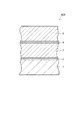
図1は、本発明による半導体基板の好適な一実施形態を示す模式断面図である。エピタキシャルウェハ100(半導体基板)は、GaAs(111)A面の基板1上に、厚さ50nmのGaNから成るバッファ層2(第1バッファ層)、厚さ25μmのGaNから成るエピタキシャル層3(第1エピタキシャル層)、厚さ50nmのGaNから成るバッファ層4(第2バッファ層)、及び厚さ25μmのGaNから成るエピタキシャル層5(第2エピタキシャル層)がこの順に積層された2段構造のものである。
【0020】
このように構成されるエピタキシャルウェハ100は、例えば以下に示す方法で製造することができる。なお、ここでは、図2に示すCVD装置20を成膜装置として用いた。図2は、当該CVD装置20の構成を示す概略図である。CVD装置20は、第1ガス導入口21と第2ガス導入口22と排気口23とが設けられた石英製の反応チャンバ24と、この反応チャンバ24の外部から反応チャンバ24内全体を加熱するための抵抗加熱ヒーター25とを備えている。また、反応チャンバ24の内部における第1ガス導入口21に対応する位置には、ガリウムメタル26が設置されるソースボート27が装着されている。
【0021】
このようなCVD装置20を用い、まず、反応チャンバ24内の所定位置に基板1を載置する。次に、抵抗加熱ヒーター25により外部から反応チャンバ24内全体を加熱して、基板1を500℃に保持した状態で、第1ガス導入口21からHClを供給する。これにより、HClが約800℃に加熱されたソースボート27内に設置されたGaと化学反応を生じてIII族ガスが発生し、そのIII族ガスが基板1上に供給される。
【0022】
一方、第2ガス導入口22からV族原料としてのNH3ガスを導入する。なお、このときの原料ガスのV族/III族比は例えば200とする。これにより、基板1上にGaN結晶をエピタキシャル成長させ、所定時間成膜してバッファ層2を形成する。
【0023】
次に、バッファ層2が形成された基板1の温度が800℃となるように、抵抗加熱ヒーター25により反応チャンバ24内全体を昇温した後、HCl及びNH3をバッファ層2上に導入する。なお、このときの原料ガスのV族/III族比は例えば200とする。これにより、バッファ層2上にGaN結晶をエピタキシャル成長させ、所定時間成膜してエピタキシャル層3を形成する。この時点で、エピタキシャル層3の観察及び評価を行ったところ、エピタキシャル層3は平坦性に極めて優れており、格子のズレが緩和されていることが確認された。
【0024】
次いで、バッファ層2が形成された基板1の温度が再び500℃となるように、抵抗加熱ヒーター25の温度調節を行って反応チャンバ24内全体を降温した後、HCl及びNH3をバッファ層2上に導入し、バッファ層2を形成したのと同様にして、エピタキシャル層3上にバッファ層4を形成する。さらにその後、抵抗加熱ヒーター25の温度調節を行って反応チャンバ24内全体を再び昇温し、バッファ層4が形成された基板1の温度が800℃となるようにし、上述したエピタキシャル層3を形成したのと同様にして、バッファ層4上にエピタキシャル層5を形成する。
【0025】
また、他の方法として、反応チャンバ24内にソースボート27を設置せず、第1ガス導入口21からTEG又はTMGとHClとを導入し、それらを化学反応させる有機金属ハライド系CVD法を用いてもよい。
【0026】
図3は、この場合に用いられるCVD装置30の構成を示す概略図である。CVD装置30は、第1ガス導入口31と第2ガス導入口32と排気口33とが設けられた石英製の反応チャンバ34と、この反応チャンバ34の外部から反応チャンバ34内全体を加熱するための抵抗加熱ヒーター35とを備えており、ソースボート27を有しないこと以外は、CVD装置20と同様の構成を有する。
【0027】
この場合、まず、反応チャンバ34内所定位置に基板1を載置する。次に、抵抗加熱ヒーター35により外部から反応チャンバ34内全体を加熱して、基板1を500℃に保持した状態で、第1ガス導入口31からTEG又はTMGとHClを供給すると共に、第2ガス導入口32からV族原料としてのNH3ガスを導入する。なお、このときの原料ガスのV族/III族比は例えば200とする。これにより、基板1上にGaN結晶をエピタキシャル成長させ、所定時間成膜してバッファ層2を形成する。
【0028】
次に、バッファ層2が形成された基板1の温度が800℃となるように、抵抗加熱ヒーター35により反応チャンバ34内全体を昇温した後、TEG又はTMGとHCl、及びNH3をバッファ層2上に導入する。なお、このときの原料ガスのV族/III族比は例えば200とする。これにより、バッファ層2上にGaN結晶をエピタキシャル成長させ、所定時間成膜してエピタキシャル層3を形成する。この時点で、エピタキシャル層3の観察及び評価を行ったところ、エピタキシャル層3は平坦性に極めて優れており、格子のズレが緩和されていることが確認された。
【0029】
次いで、バッファ層2が形成された基板1の温度が再び500℃となるように、抵抗加熱ヒーター35の温度調節を行って反応チャンバ34内全体を降温した後、TEG又はTMGとHCl、及びNH3をバッファ層2上に導入し、上述したバッファ層2を形成したのと同様にして、エピタキシャル層3上にバッファ層4を形成する。さらにその後、抵抗加熱ヒーター35の温度調節を行って反応チャンバ34内全体を再び昇温し、バッファ層4が形成された基板1の温度が800℃となるようにし、上述したエピタキシャル層3を形成したのと同様にして、バッファ層4上にエピタキシャル層5を形成する。
【0030】
ここで、このようにして得たエピタキシャル層3,5の光学特性を評価すべく、エピタキシャルウェハ100に対してフォトルミネッセンス(PL)法を実施した。比較のため同様な方法で形成したバッファ層2とエピタキシャル層3のみを有する1段構造のエピタキシャルウェハについても同様の測定を実施した。なお、測定は室温で行った。
【0031】
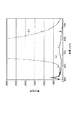
図4は、エピタキシャルウェハの発光スペクトルを示すグラフである。同図の横軸はエピタキシャルウェハからの発光波長を示し、縦軸はその発光強度を示す。図中、曲線L1,L2は、それぞれエピタキシャルウェハ100及び比較例のエピタキシャルウェハの発光スペクトルを示す。また、波長360nm付近に存在するピークはバンド端からの発光に相当する。また、波長570nm付近に存在するピークは、一般に‘イエロピーク’と呼ばれるものであり、結晶のストイキオメトリのズレに起因するピークと目されており、この強度が低い程、良好な結晶が形成されていることを示唆するものである。
【0032】
これらの結果より、本発明の2段構造を有するエピタキシャルウェハ100は、比較例のウェハに比して波長360nm付近のバンド端発光の強度が強く、より良好な結晶品質を有することが確認された。また、本発明の2段構造を有するエピタキシャルウェハ100は、比較例のウェハに比して波長570nm付近の‘イエロピーク’強度が低く、このことからも1段構造を有する比較例のウェハ比して結晶品質が著しく改善されていることが判明した。
【0033】
さらに、バッファ層2,4及びエピタキシャル層3,5の転位状態を評価すべく、エピタキシャルウェハ100の結晶断面のTEM観察を実施した。図5は、エピタキシャルウェハ100における第2層目であるバッファ層4近傍の断面TEM写真を示す。これより、線状の転位がバッファ層2,4により低減されていることが判明した。
【0034】
【発明の効果】
以上説明したように、本発明の半導体基板及びその製造方法によれば、ハロゲン化物を含む反応系を用いたCVD法によってバッファ層及びエピタキシャル層の交互積層による2段構造が形成されて成るので、エピタキシャル層の転位を抑制して十分な格子緩和効果を得ることができる。また、このような本発明の半導体基板を用いることにより、良質のGaN結晶層を形成でき、その結果、信頼性に優れた半導体レーザ素子や青色レーザダイオード等の発光素子を得ることができる。
【図面の簡単な説明】
【図1】本発明による半導体基板の好適な一実施形態を示す模式断面図である。
【図2】CVD装置20の構成を示す概略図である。
【図3】CVD装置30の構成を示す概略図である。
【図4】エピタキシャルウェハの発光スペクトルを示すグラフである。
【図5】エピタキシャルウェハ100におけるバッファ層4近傍の断面TEM写真を示す。
【符号の説明】
1…基板、2…バッファ層(第1バッファ層)、3…エピタキシャル層(第1エピタキシャル層)、4…バッファ層(第2バッファ層)、5…エピタキシャル層(第2エピタキシャル層)、20,30…CVD装置、24,34…反応チャンバ、100…エピタキシャルウェハ(半導体基板)。[0001]
TECHNICAL FIELD OF THE INVENTION
The present invention relates to a semiconductor substrate and a method for manufacturing the same, and more particularly, to a semiconductor substrate such as an epitaxial wafer suitable for forming a light emitting element such as a semiconductor laser element and a blue laser diode, and a method for manufacturing the same.
[0002]
[Prior art]
In recent years, there has been an increasing need for blue LEDs and lasers for use in color displays and optical discs, and GaN-based materials have been spotlighted as materials that emit light in the blue or ultraviolet region. As a substrate for forming such a GaN-based epitaxial film, it is desirable to use a GaN substrate lattice-matched with the epitaxial film to be formed, but it is very difficult to manufacture such a GaN substrate. Therefore, a sapphire substrate whose lattice constant is relatively close to that of a GaN-based epitaxial film is generally used. Further, in order to alleviate this lattice shift, a buffer layer made of GaN or AlN grown at a low temperature is usually used.
[0003]
In addition, regarding the conventional GaN-based epitaxial crystal, a single (single) low-temperature buffer layer is formed to suppress dislocation due to lattice shift, and there are reports on the effect of the low-temperature GaN buffer layer (for example, Non-Patent Document 1). However, the lattice displacement mitigation method using such a low-temperature buffer layer does not sufficiently suppress the dislocation generated due to the lattice displacement, and has a problem in reliability, for example, when a blue laser device is manufactured.
[0004]
In order to solve such inconveniences, various techniques for further suppressing the generation of dislocations due to lattice mismatch have been tried. One of them is to use a metal-organic vapor phase epitaxy (MO-CVD) method to form a low-temperature buffer layer. Is reported to have a two-stage (double) configuration (for example, see Non-Patent Document 2).
[0005]
[Non-patent document 1]
J. Appl. Phys. 71 (1992) 5543
[Non-patent document 2]
Jpn. J. Appl. Phys. Vol. 37 (1998) pp. L316-L318
[0006]
[Problems to be solved by the invention]
However, when a GaN-based epitaxial film is grown on a two-stage low-temperature buffer layer made of GaN formed using such a technique, an epitaxial layer having a sufficient thickness tends to be unable to grow. For example, the thicknesses of the buffer layer and the epitaxial layer according to Non-Patent
[0007]
Therefore, the present invention has been made in view of such circumstances, and provides a semiconductor substrate capable of obtaining a sufficient lattice relaxation effect and capable of obtaining a highly reliable light emitting element, and a method of manufacturing the same. Aim.
[0008]
[Means for Solving the Problems]
In order to solve the above problems, a semiconductor substrate according to the present invention includes a substrate made of a compound semiconductor, a first buffer layer mainly made of GaN formed on the substrate, and a GaN formed on the first buffer layer. A first epitaxial layer comprising GaN, a second buffer layer mainly comprising GaN formed on the first epitaxial layer, and a second epitaxial layer comprising GaN formed on the second buffer layer. In this case, the first buffer layer and the second buffer layer are formed by a vapor deposition method using a reaction system containing a halide.
[0009]
In a semiconductor substrate having such a structure, the growth rate of each layer can be increased by using a CVD method using a reaction system containing a halide, that is, a halogen-based CVD method, as compared with the MO-CVD method. Specifically, the film formation rate by the halogen-based CVD method is about 10 of the MO-CVD method. The present inventor has confirmed that the thickness of the first and second epitaxial layers on the first and second buffer layers thus formed can be significantly increased as compared with the related art. The detailed mechanism of whether this is only due to the formation of the first and second buffer layers at a high deposition rate, or whether the increase in the deposition rate of the first and second epitaxial layers is also related is not yet known. However, in addition to the increase in deposition rate, other factors such as the adhesion of the buffer layer and the epitaxial layer formed by the halogen-based CVD method, the influence of the film thickness, and the presence or absence of nucleation are also complicatedly related. I cannot deny the possibility of doing it.
[0010]
Specific examples of the halogen-based CVD method include a hydride CVD method using metal Ga and HCl as a group III raw material and NH 3 as a group V raw material, and an organic metal containing Ga as a group III raw material (for example, trimethylgallium). ; (CH3) 3 Ga or triethyl gallium; (C 2 H 5) 3 Ga) and halogen-CVD method using NH 3 as HCl and V group material and the like.
[0011]
Specifically, the plane orientation of the substrate is preferably the (111) A plane. More specifically, it is preferable that the substrate is made of a group III-V compound semiconductor, and it is particularly useful that the group III-V compound semiconductor is GaAs or InP.
[0012]
More preferably, the thickness of the first buffer layer is 10 to 100 nm, and the thickness of the second buffer layer is 5 to 70 nm. If the thickness of the first buffer layer is less than 10 nm, the first buffer layer tends to be partially interrupted during the temperature rise for forming the first epitaxial layer, and when this occurs, it is formed thereon. The first epitaxial layer may peel off. On the other hand, when the thickness of the first buffer layer exceeds 100 nm, nucleation (nucleation) tends to occur during the growth of the first buffer layer where flatness is required. The layer tends to grow in a pyramid shape, which is not preferable.
[0013]
Then, from the viewpoint of exhibiting a sufficient lattice relaxation effect, the thickness of the first or second epitaxial layer is desirably 20 to 1000 μm.
[0014]
Further, the method for manufacturing a semiconductor substrate according to the present invention is a method for effectively manufacturing the semiconductor substrate according to the present invention, wherein (a) a method of manufacturing a semiconductor substrate on a substrate made of a compound semiconductor under an environment heated to a first temperature. Supplying a first gas containing a halide, a second gas containing Ga, and a third gas containing NH 3 to form a first buffer layer mainly composed of GaN; Supplying the first to third gases in an environment heated to a second temperature higher than the temperature of (a) to form a first epitaxial layer containing GaN on the first buffer layer; (C) supplying first to third gases in an environment heated to a first temperature to form a second buffer layer mainly composed of GaN on the first epitaxial layer; In an environment heated to a temperature of 2, the first to third And forming a second epitaxial layer containing GaN on the second buffer layer.
[0015]
In this case, it is preferable that the first temperature be a temperature in the range of 300 to 700 ° C. and the second temperature be 750 ° C. or higher. If the first temperature (film formation temperature) when forming the first buffer layer is lower than 300 ° C., the first buffer layer mainly composed of GaN tends to be insufficiently grown. On the other hand, when the first temperature exceeds 700 ° C., the amount of heat input to the substrate increases, the thermal budget deteriorates, and the first buffer layer receives thermal damage. There is a possibility that the epitaxial layer is peeled off.
[0016]
Specifically, it is preferable to use HCl gas as the first gas. More specifically, a substrate having a plane orientation of (111) A is used as the substrate, and more specifically, a substrate of III-V It is preferable to use a group III-V compound semiconductor, and it is particularly useful to use a group III-V compound semiconductor of GaAs or InP.
[0017]
Furthermore, the thickness of the first buffer layer is 10 to 100 nm, the thickness of the second buffer layer is 5 to 70 nm, and the thickness of the first or second epitaxial layer is 10 to 100 nm. It is desirable to adjust the process conditions in each step so as to be 20 to 1000 μm.
[0018]
BEST MODE FOR CARRYING OUT THE INVENTION
Hereinafter, embodiments of the present invention will be described in detail. The positional relationship such as up, down, left, and right is based on the positional relationship shown in the drawings unless otherwise specified. The dimensional ratios in the drawings are not limited to the illustrated ratios.
[0019]
FIG. 1 is a schematic sectional view showing a preferred embodiment of a semiconductor substrate according to the present invention. The epitaxial wafer 100 (semiconductor substrate) has a buffer layer 2 (first buffer layer) made of GaN having a thickness of 50 nm and an epitaxial layer 3 (first buffer layer) made of GaN having a thickness of 25 μm on a GaAs (111) A plane substrate 1. 1), a
[0020]
The
[0021]
First, the substrate 1 is placed at a predetermined position in the
[0022]
On the other hand, NH 3 gas as a group V material is introduced from the
[0023]
Next, after heating the entire inside of the
[0024]
Then, as the temperature of the substrate 1,
[0025]
As another method, an organic metal halide CVD method in which TEG or TMG and HCl are introduced from the
[0026]
FIG. 3 is a schematic diagram showing the configuration of the
[0027]
In this case, first, the substrate 1 is placed at a predetermined position in the
[0028]
Next, after heating the entire inside of the
[0029]
Next, the temperature of the
[0030]
Here, a photoluminescence (PL) method was performed on the
[0031]
FIG. 4 is a graph showing an emission spectrum of the epitaxial wafer. The horizontal axis in the figure indicates the emission wavelength from the epitaxial wafer, and the vertical axis indicates the emission intensity. In the figure, curves L1 and L2 indicate the emission spectra of the
[0032]
From these results, it was confirmed that the
[0033]
Further, TEM observation of a crystal cross section of the
[0034]
【The invention's effect】
As described above, according to the semiconductor substrate and the method for manufacturing the same of the present invention, a two-stage structure is formed by alternately laminating a buffer layer and an epitaxial layer by a CVD method using a reaction system containing a halide. A sufficient lattice relaxation effect can be obtained by suppressing dislocations in the epitaxial layer. In addition, by using such a semiconductor substrate of the present invention, a high-quality GaN crystal layer can be formed, and as a result, a light emitting element such as a semiconductor laser element or a blue laser diode having excellent reliability can be obtained.
[Brief description of the drawings]
FIG. 1 is a schematic sectional view showing a preferred embodiment of a semiconductor substrate according to the present invention.
FIG. 2 is a schematic diagram illustrating a configuration of a
FIG. 3 is a schematic diagram illustrating a configuration of a
FIG. 4 is a graph showing an emission spectrum of the epitaxial wafer.
FIG. 5 shows a TEM photograph of a cross section near the
[Explanation of symbols]
DESCRIPTION OF SYMBOLS 1 ... board | substrate, 2 ... buffer layer (1st buffer layer), 3 ... epitaxial layer (1st epitaxial layer), 4 ... buffer layer (2nd buffer layer), 5 ... epitaxial layer (2nd epitaxial layer), 20, Reference numeral 30: CVD apparatus, 24, 34: reaction chamber, 100: epitaxial wafer (semiconductor substrate).
Claims (13)
前記基板上に形成された主としてGaNから成る第1バッファ層と、
前記第1バッファ層上に形成されたGaNを含んで成る第1エピタキシャル層と、
前記第1エピタキシャル層上に形成された主としてGaNから成る第2バッファ層と、
前記第2バッファ層上に形成されたGaNを含んで成る第2エピタキシャル層と、を備えており、
前記第1バッファ層及び第2バッファ層が、ハロゲン化物を含む反応系を用いた気相成長法により形成されたものである半導体基板。A substrate made of a compound semiconductor;
A first buffer layer mainly made of GaN formed on the substrate;
A first epitaxial layer comprising GaN formed on the first buffer layer;
A second buffer layer mainly composed of GaN formed on the first epitaxial layer;
A second epitaxial layer comprising GaN formed on the second buffer layer,
A semiconductor substrate, wherein the first buffer layer and the second buffer layer are formed by a vapor deposition method using a reaction system containing a halide.
前記第1の温度よりも高い第2の温度に加熱された環境下で、前記第1〜第3のガスを供給し、前記第1バッファ層上にGaNを含有して成る第1エピタキシャル層を形成するステップと、
前記第1の温度に加熱された環境下で、前記第1〜第3のガスを供給し、前記第1エピタキシャル層上に主としてGaNから成る第2バッファ層を形成するステップと、
前記第2の温度に加熱された環境下で、前記第1〜第3のガスを供給し、前記第2バッファ層上にGaNを含有して成る第2エピタキシャル層を形成するステップと、
を備える半導体基板の製造方法。In an environment heated to a first temperature, a first gas containing a halide, a second gas containing Ga, and a third gas containing NH 3 are supplied onto a substrate made of a compound semiconductor, mainly Forming a first buffer layer comprising GaN;
In an environment heated to a second temperature higher than the first temperature, the first to third gases are supplied to form a first epitaxial layer containing GaN on the first buffer layer. Forming;
Supplying the first to third gases under an environment heated to the first temperature to form a second buffer layer mainly composed of GaN on the first epitaxial layer;
Supplying the first to third gases under an environment heated to the second temperature to form a second epitaxial layer containing GaN on the second buffer layer;
A method for manufacturing a semiconductor substrate comprising:
請求項7〜12のいずれか一項に記載の半導体基板の製造方法。The first buffer layer has a thickness of 10 to 100 nm, the second buffer layer has a thickness of 5 to 70 nm, and the first or second epitaxial layer has a thickness of 10 to 100 nm. Adjusting the process conditions in each of the steps so as to be 20 to 1000 μm;
A method for manufacturing a semiconductor substrate according to claim 7.
Priority Applications (1)
| Application Number | Priority Date | Filing Date | Title |
|---|---|---|---|
| JP2002275882A JP2004111865A (en) | 2002-09-20 | 2002-09-20 | Semiconductor substrate and its fabricating process |
Applications Claiming Priority (1)
| Application Number | Priority Date | Filing Date | Title |
|---|---|---|---|
| JP2002275882A JP2004111865A (en) | 2002-09-20 | 2002-09-20 | Semiconductor substrate and its fabricating process |
Publications (1)
| Publication Number | Publication Date |
|---|---|
| JP2004111865A true JP2004111865A (en) | 2004-04-08 |
Family
ID=32271949
Family Applications (1)
| Application Number | Title | Priority Date | Filing Date |
|---|---|---|---|
| JP2002275882A Pending JP2004111865A (en) | 2002-09-20 | 2002-09-20 | Semiconductor substrate and its fabricating process |
Country Status (1)
| Country | Link |
|---|---|
| JP (1) | JP2004111865A (en) |
Cited By (4)
| Publication number | Priority date | Publication date | Assignee | Title |
|---|---|---|---|---|
| WO2012162196A2 (en) * | 2011-05-20 | 2012-11-29 | Applied Materials, Inc. | Methods for improved growth of group iii nitride buffer layers |
| US8853086B2 (en) | 2011-05-20 | 2014-10-07 | Applied Materials, Inc. | Methods for pretreatment of group III-nitride depositions |
| US8980002B2 (en) | 2011-05-20 | 2015-03-17 | Applied Materials, Inc. | Methods for improved growth of group III nitride semiconductor compounds |
| CN108140561A (en) * | 2015-11-02 | 2018-06-08 | 日本碍子株式会社 | The manufacturing method of epitaxial substrate for semiconductor device, semiconductor element and epitaxial substrate for semiconductor device |
-
2002
- 2002-09-20 JP JP2002275882A patent/JP2004111865A/en active Pending
Cited By (8)
| Publication number | Priority date | Publication date | Assignee | Title |
|---|---|---|---|---|
| WO2012162196A2 (en) * | 2011-05-20 | 2012-11-29 | Applied Materials, Inc. | Methods for improved growth of group iii nitride buffer layers |
| WO2012162196A3 (en) * | 2011-05-20 | 2013-01-24 | Applied Materials, Inc. | Methods for improved growth of group iii nitride buffer layers |
| CN103548117A (en) * | 2011-05-20 | 2014-01-29 | 应用材料公司 | Methods for improved growth of group iii nitride buffer layers |
| US8778783B2 (en) | 2011-05-20 | 2014-07-15 | Applied Materials, Inc. | Methods for improved growth of group III nitride buffer layers |
| US8853086B2 (en) | 2011-05-20 | 2014-10-07 | Applied Materials, Inc. | Methods for pretreatment of group III-nitride depositions |
| US8980002B2 (en) | 2011-05-20 | 2015-03-17 | Applied Materials, Inc. | Methods for improved growth of group III nitride semiconductor compounds |
| CN108140561A (en) * | 2015-11-02 | 2018-06-08 | 日本碍子株式会社 | The manufacturing method of epitaxial substrate for semiconductor device, semiconductor element and epitaxial substrate for semiconductor device |
| CN108140561B (en) * | 2015-11-02 | 2022-04-12 | 日本碍子株式会社 | Epitaxial substrate for semiconductor element, and method for manufacturing epitaxial substrate for semiconductor element |
Similar Documents
| Publication | Publication Date | Title |
|---|---|---|
| JP4529846B2 (en) | III-V nitride semiconductor substrate and method for manufacturing the same | |
| JP4563230B2 (en) | Method for manufacturing AlGaN substrate | |
| JP4901145B2 (en) | Compound semiconductor device and manufacturing method thereof | |
| TWI519686B (en) | New process for growth of low dislocation density gan | |
| JP5276852B2 (en) | Method for manufacturing group III nitride semiconductor epitaxial substrate | |
| JP4189386B2 (en) | Method for growing nitride semiconductor crystal layer and method for producing nitride semiconductor light emitting device | |
| JP2006128626A (en) | Nitride semiconductor device and its manufacturing method | |
| JP2009505938A (en) | Semiconductor substrate, method for manufacturing a self-supporting semiconductor substrate by hydride vapor phase epitaxy, and mask layer used therefor | |
| US20110003420A1 (en) | Fabrication method of gallium nitride-based compound semiconductor | |
| WO2010113423A1 (en) | Method for growing crystals of nitride semiconductor, and process for manufacture of semiconductor device | |
| JP4860736B2 (en) | Semiconductor structure and method of manufacturing the same | |
| US7462505B2 (en) | Growth process of a crystalline gallium nitride based compound and semiconductor device including gallium nitride based compound | |
| US6648966B2 (en) | Wafer produced thereby, and associated methods and devices using the wafer | |
| JP4734786B2 (en) | Gallium nitride compound semiconductor substrate and manufacturing method thereof | |
| JPH09134878A (en) | Manufacture of gallium nitride compound semiconductor | |
| JP4996448B2 (en) | Method for creating a semiconductor substrate | |
| US7589345B2 (en) | Nitride-based compound semiconductor substrate and method for fabricating the same | |
| JPH07201745A (en) | Semiconductor wafer and its manufacture | |
| JPH11135889A (en) | Substrate for crystal growth and light-emitting device using the same | |
| JP2009067658A (en) | Nitride semiconductor ground substrate, nitride semiconductor-stacked substrate, nitride semiconductor self-standing substrate and method for producing nitride semiconductor ground substrate | |
| JP2005210084A (en) | Epitaxial substrate, semiconductor laminate structure, dislocation reduction method, and substrate for epitaxial formation | |
| JP4424497B2 (en) | Method for manufacturing nitride semiconductor crystal | |
| JP2009023853A (en) | Group iii-v nitride semiconductor substrate, method for manufacturing the same, and group iii-v nitride semiconductor device | |
| JP4679810B2 (en) | EPITAXIAL SUBSTRATE, SEMICONDUCTOR LAMINATED STRUCTURE, EPITAXIAL SUBSTRATE MANUFACTURING METHOD, AND METHOD FOR SUPPRESSING PIT GENERATION ON Epitaxial Substrate Surface | |
| JP2004111865A (en) | Semiconductor substrate and its fabricating process |