【0001】
【発明の属する技術分野】
本発明は半導体薄膜の製造方法に関する。
【0002】
【従来の技術】
例えば、マイクロマシン(MEMS:Micro−Electro−Mechanical−System)は、基板上に酸化膜層を介して半導体その他の材料からなる構造体を有している。例えばアクチュエータとしては、酸化膜層上に形成されたシリコンからなる対向する櫛形状の電極を備え、電極間に電圧を印加することによって電極間の距離を変化させるタイプのものが知られている。そして、このような電極等の構造体は可動部であることから、直接には樹脂モールドされていない。
【0003】
【発明が解決しようとする課題】
この櫛形状の電極のように、半導体材料からなる微小な構造体若しくは回路がモールドされずに環境雰囲気に晒された場合、印加される電圧が比較的大きいことや、酸化膜層が薄くかつ基板自体が半導体材料からなることから、絶縁不良が起こりやすいという問題がある。
【0004】
また、構造体を外部と電気的に接続するための配線は、構造体が形成されている側の基板表面ではなく、基板に穿孔されたスルーホールを通して構造体とは反対側の基板表面から引き出される。しかしながら、半導体材料からなる基板の場合、スルーホール間での絶縁性が十分に確保されないという問題がある。
そこで絶縁性を確保するために、基板材料として、例えば、ガラスからなる絶縁基板を使用することが好適であるが、その場合には、絶縁基板の表面に良質な結晶性を有する薄膜をエピタキシャル成長させることができない。また成長させることができた場合でも、絶縁基板の反りやうねりに起因し、均一な膜厚を有する薄膜を基板上に形成することが困難であるという問題がある。
【0005】
本発明は、上記した問題を解決し、均一な膜厚と良質な結晶性を有する半導体薄膜の絶縁基板上への形成方法の提供を目的とする。
【0006】
【課題を解決するための手段】
上記した目的を達成するために、本発明においては、半導体基板、および、この半導体基板の表面に位置し、少なくとも前記半導体基板の表面とは反対側に半導体薄膜層を含む転写層を備える転写基板を前記半導体薄膜層側にて絶縁基板に接合する工程と、前記絶縁基板に接合された前記転写基板の前記半導体基板側を前記半導体薄膜層まで除去する工程とを備えることを特徴とする絶縁基板上への半導体薄膜の形成方法が提供される。
【0007】
【発明の実施の形態】
本発明の絶縁基板上への半導体薄膜の製造方法は、例えば、環境雰囲気に晒される構造体もしくは回路が絶縁基板上に形成される、アクチュエータ、モータ等のマイクロマシン、温度、圧力、加速度センサ等の半導体センサ、湿度、CO2センサ等のガスセンサ等の製造工程において用いられる。
【0008】
以下、本発明に係る絶縁基板上への半導体薄膜の製造方法(以下、単に製造方法Aという)を図面に基づいて説明する。
製造方法Aにおいては、まず、図1(a)に示した転写基板10と、絶縁基板とを用意する。転写基板10は、半導体基板12を備え、この半導体基板12の一方の表面には、転写層14が形成されている。転写層14は、犠牲層16及び結晶性を有する単結晶若しくは多結晶の半導体薄膜層18を含んでいる。犠牲層16は転写層14の半導体基板12側に位置している。また、半導体薄膜層18は、転写層14の半導体基板12とは反対側に位置し、転写基板10の一方の側にて表出している。
【0009】
半導体基板12は、例えば厚みが100〜1000μm程度であって、その材料としては、シリコン、GaAs、GaN、およびInP等を挙げることができる。
犠牲層16は、後述するように、半導体薄膜層18に対しては不活性であるエッチング処理によって除去される材料からなる。このような材料は、半導体薄膜層18の材料に応じて適宜選択することができるが、例えば、酸化シリコンを挙げることができる。
【0010】
半導体薄膜層18は、エピタキシャル成長された単結晶若しくは多結晶膜であって、例えば、厚みが0.01〜20μm程度、面内方向での厚みの標準偏差が0.001〜0.01μm程度である。そして、半導体薄膜層18の材料としては、シリコン、GaAs、GaN、およびInP等を挙げることができ、これら半導体材料は真性半導体又はP型半導体若しくはN型等の不純物半導体のいずれであっても良い。
【0011】
なお、半導体薄膜層18は、それ自体が多層構造を有していても良い。例えば、半導体薄膜層18の絶縁基板に接合される表面には、絶縁基板の線膨張係数に近い線膨張係数を有する材料からなるバッファ層を設けても良い。これにより、絶縁基板とその上に形成された半導体薄膜との間の密着性を高めることができる。
【0012】
また、半導体基板12及び半導体薄膜層18の両者がシリコンからなり、半導体薄膜層18のみが高濃度の不純物を含む場合、転写層14は、犠牲層16を含まなくとも良い。なぜならば、高濃度に不純物を含むシリコンと含まないシリコンとでは、互いにエッチングレートが大きく異なり、半導体薄膜層18をほとんど除去することなく、半導体基板12のみを選択的に除去できるからである。
【0013】
絶縁基板は、例えば厚みが100〜1000μm程度であって、その材料としては、ガラス、石英、サファイア、窒化アルミ(AlN)、窒化ホウ素(BN)ジルコニア、およびサイアロン等を挙げることができる。
次に、用意した転写基板10と絶縁基板とを接合して中間製品20を作成する。具体的には、図1(b)に示したように、転写基板10の半導体薄膜層18側の表面を絶縁基板22の一方の表面に接合する。
【0014】
ここで、基板10,22同士の接合方法としては、これら基板間に電圧を印可する陽極酸化法、または、直接接合法等の公知の方法を用いることができる。
そして、得られた中間製品20から、転写基板10の半導体基板12側を半導体薄膜層18まで除去する。換言すれば、転写基板10の半導体薄膜層18以外の部分、すなわち半導体基板12及び犠牲層16を除去する。これによって、絶縁基板22上に半導体薄膜層18が転写され、絶縁基板22上に半導体薄膜が形成される(図1(c)、(d)参照)。
【0015】
これら半導体基板12及び犠牲層16を除去する方法としては、公知の方法を用いることができる。例えば、半導体基板12を除去するにあたっては、研磨及びエッチング処理等を用いることができ、犠牲層16を除去するにあたっては、エッチング処理を用いることができる。
この製造方法Aによれば、絶縁基板22上の半導体薄膜の結晶性、膜厚およびその標準偏差は、転写基板10における半導体薄膜層18のそれら物性に直接依存する一方、絶縁基板には無依存である。したがって、製造方法Aによれば、良質な結晶性を有し、均一な膜厚を有する半導体薄膜を絶縁基板上に容易に形成することができる。
【0016】
【実施例】
実施例1
転写基板10として、市販されている信越半導体(株)製のSOI(Silicon on Insulator)基板を、また絶縁基板22として旭ガラス(株)製のガラス基板を使用して、製造方法Aにより絶縁基板上に半導体薄膜を形成した。
【0017】
なお、SOI基板は、半導体基板12としてのSi基板上に犠牲層16として酸化シリコンからなるボックス層を有し、ボックス層のSi基板とは反対側に、単結晶の半導体薄膜層18としてSi層を有している。このSi層は、厚みが5μmであって、膜厚の誤差は±0.5μm以内に収められている。
用意したSOI基板とガラス基板との間の接合には、陽極酸化法を使用した。その際、基板間には、300Vの電圧を印加した。
【0018】
そして、SOI基板とガラス基板とが接合された中間製品のSOI基板側を研磨して、Si基板の厚みが100μm以下となるまで研磨した後、KOH水溶液にてエッチング処理してSi基板を全て除去した。その後、ボックス層をフッ酸を用いてエッチング処理して、ガラス基板上に単結晶Si薄膜を形成した。
実施例2
製造方法Aを使用して静電容量型の湿度センサを製造した。
【0019】
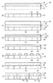
転写基板10として、市販されている信越半導体(株)製のSOI基板(図2(a)参照)を、また絶縁基板22として旭ガラス(株)製のガラス基板(図2(b)参照)を使用した。ここで、ガラス基板には、厚み方向に貫通して基板の両面にて開口するスルーホールが基板の面内方向にみて所定の間隔を置いて形成されている。
【0020】
用意したSOI基板とガラス基板との間の接合には、陽極酸化法を使用した。その際、基板間には、300Vの電圧を印加した(図2(c)参照)。
そして、SOI基板とガラス基板とが接合された中間製品のSOI基板側を研磨して、Si基板の厚みが100μm以下となるまで研磨した後、KOH水溶液にてエッチング処理してSi基板を全て除去した(図2(d)参照)。その後、ボックス層をフッ酸水溶液を用いてエッチング処理して、ガラス基板上に単結晶Si薄膜を形成した(図2(e)参照)。
【0021】
このSi薄膜上に、SiN膜をCVD法により成膜してからその上に所定パターンを有するレジスト膜を作成し、RIEによりレジスト膜を介してSiN膜を所定パターンにした。そして、レジスト膜を除去してからSi薄膜をKOH水溶液にてエッチング処理して所望パターンにした後、SiN膜を除去した(図2(f)参照)。
【0022】
その後に、このSi薄膜のパターンを架橋ポリイミドからなる感湿膜26で被い(図2(g)参照)、ガラス基板とともにダイシング処理して複数の素子に分離し、ガラス基板のスルーホール24に導電性接着剤を充填して配線28を形成した(図2(h)参照)。
このようにして製造された、一つのガラス基板から製造された同一ロットの30個の湿度センサを恒温恒湿度槽内に配置して、各湿度センサが示した静電容量の標準偏差を求めた。その結果、標準偏差は非常に小さく、ガラス基板上に形成されたSi薄膜が均一な膜厚を有することがわかった。また、各湿度センサのスルーホール間の抵抗値についても調べたところ、これら湿度センサは十分な絶縁性を有していることがわかった。
【0023】
なお、本発明は上記した実施例に限定されることはなく、種々変形が可能である。
【0024】
【発明の効果】
以上の説明で明らかなように、本発明の絶縁基板上への半導体薄膜の形成方法によれば、均一な膜厚及び良好な結晶性を有する半導体薄膜を絶縁基板上に形成することができる。
【図面の簡単な説明】
【図1】本発明に係る絶縁基板上への半導体薄膜の形成方法の概略工程図である。
【図2】図1の方法を適用した湿度センサの製造方法の概略工程図である。
【符号の説明】
10 転写基板
12 半導体基板
14 転写層
18 半導体薄膜層
22 絶縁基板[0001]
TECHNICAL FIELD OF THE INVENTION
The present invention relates to a method for manufacturing a semiconductor thin film.
[0002]
[Prior art]
For example, a micro machine (MEMS: Micro-Electro-Mechanical-System) has a structure made of a semiconductor or other material on a substrate via an oxide film layer. For example, as an actuator, a type is known which includes opposing comb-shaped electrodes made of silicon formed on an oxide film layer and changes the distance between the electrodes by applying a voltage between the electrodes. And since such a structure, such as an electrode, is a movable part, it is not directly resin-molded.
[0003]
[Problems to be solved by the invention]
When a minute structure or circuit made of a semiconductor material such as a comb-shaped electrode is exposed to an environmental atmosphere without being molded, the applied voltage is relatively large, or the oxide film layer is thin and the substrate is thin. Since it is made of a semiconductor material, there is a problem that insulation failure easily occurs.
[0004]
In addition, wiring for electrically connecting the structure to the outside is drawn not through the surface of the substrate on which the structure is formed but through the through-hole formed in the substrate from the surface of the substrate opposite to the structure. It is. However, in the case of a substrate made of a semiconductor material, there is a problem that insulation between the through holes is not sufficiently ensured.
Therefore, in order to ensure insulation, it is preferable to use an insulating substrate made of glass, for example, as a substrate material. In this case, a thin film having good crystallinity is epitaxially grown on the surface of the insulating substrate. I can't. Further, even when the insulating substrate can be grown, there is a problem that it is difficult to form a thin film having a uniform thickness on the substrate due to warpage or undulation of the insulating substrate.
[0005]
An object of the present invention is to solve the above-mentioned problems and to provide a method of forming a semiconductor thin film having a uniform thickness and good crystallinity on an insulating substrate.
[0006]
[Means for Solving the Problems]
In order to achieve the above object, in the present invention, a transfer substrate comprising a semiconductor substrate and a transfer layer including a semiconductor thin film layer at least on the opposite side of the surface of the semiconductor substrate from the surface of the semiconductor substrate Bonding the semiconductor substrate to the insulating substrate on the semiconductor thin film layer side, and removing the semiconductor substrate side of the transfer substrate bonded to the insulating substrate up to the semiconductor thin film layer. A method for forming a semiconductor thin film thereon is provided.
[0007]
BEST MODE FOR CARRYING OUT THE INVENTION
The method for manufacturing a semiconductor thin film on an insulating substrate of the present invention includes, for example, a structure or a circuit exposed to an environmental atmosphere is formed on the insulating substrate, a micromachine such as an actuator or a motor, a temperature, a pressure, an acceleration sensor or the like. It is used in a manufacturing process of a gas sensor such as a semiconductor sensor, a humidity sensor and a CO 2 sensor.
[0008]
Hereinafter, a method of manufacturing a semiconductor thin film on an insulating substrate according to the present invention (hereinafter, simply referred to as manufacturing method A) will be described with reference to the drawings.
In the manufacturing method A, first, the transfer substrate 10 and the insulating substrate shown in FIG. 1A are prepared. The transfer substrate 10 includes a semiconductor substrate 12, and a transfer layer 14 is formed on one surface of the semiconductor substrate 12. The transfer layer 14 includes a sacrificial layer 16 and a single-crystal or polycrystalline semiconductor thin film layer 18 having crystallinity. The sacrificial layer 16 is located on the semiconductor substrate 12 side of the transfer layer 14. The semiconductor thin film layer 18 is located on the opposite side of the transfer layer 14 from the semiconductor substrate 12 and is exposed on one side of the transfer substrate 10.
[0009]
The semiconductor substrate 12 has a thickness of, for example, about 100 to 1000 μm, and examples of the material include silicon, GaAs, GaN, and InP.
The sacrifice layer 16 is made of a material that is removed by an etching process that is inactive with respect to the semiconductor thin film layer 18 as described later. Such a material can be appropriately selected according to the material of the semiconductor thin film layer 18, and for example, silicon oxide can be used.
[0010]
The semiconductor thin film layer 18 is an epitaxially grown single crystal or polycrystalline film, for example, having a thickness of about 0.01 to 20 μm and a standard deviation of the thickness in the in-plane direction of about 0.001 to 0.01 μm. . Examples of the material of the semiconductor thin film layer 18 include silicon, GaAs, GaN, and InP. These semiconductor materials may be any of an intrinsic semiconductor or a P-type semiconductor or an N-type impurity semiconductor. .
[0011]
The semiconductor thin film layer 18 may have a multilayer structure. For example, a buffer layer made of a material having a linear expansion coefficient close to the linear expansion coefficient of the insulating substrate may be provided on the surface of the semiconductor thin film layer 18 bonded to the insulating substrate. Thereby, the adhesion between the insulating substrate and the semiconductor thin film formed thereon can be improved.
[0012]
When both the semiconductor substrate 12 and the semiconductor thin film layer 18 are made of silicon, and only the semiconductor thin film layer 18 contains high-concentration impurities, the transfer layer 14 may not include the sacrificial layer 16. This is because silicon having a high concentration of impurities and silicon having no impurities have greatly different etching rates, and only the semiconductor substrate 12 can be selectively removed without removing the semiconductor thin film layer 18 almost completely.
[0013]
The insulating substrate has a thickness of, for example, about 100 to 1000 μm, and examples of the material include glass, quartz, sapphire, aluminum nitride (AlN), boron nitride (BN) zirconia, and sialon.
Next, the prepared transfer substrate 10 and the insulating substrate are joined to form an intermediate product 20. Specifically, as shown in FIG. 1B, the surface of the transfer substrate 10 on the semiconductor thin film layer 18 side is joined to one surface of the insulating substrate 22.
[0014]
Here, as a bonding method between the substrates 10 and 22, a known method such as an anodic oxidation method for applying a voltage between these substrates or a direct bonding method can be used.
Then, the semiconductor substrate 12 side of the transfer substrate 10 is removed to the semiconductor thin film layer 18 from the obtained intermediate product 20. In other words, portions other than the semiconductor thin film layer 18 of the transfer substrate 10, that is, the semiconductor substrate 12 and the sacrifice layer 16 are removed. Thus, the semiconductor thin film layer 18 is transferred onto the insulating substrate 22, and a semiconductor thin film is formed on the insulating substrate 22 (see FIGS. 1C and 1D).
[0015]
As a method of removing the semiconductor substrate 12 and the sacrificial layer 16, a known method can be used. For example, in removing the semiconductor substrate 12, polishing and etching can be used, and in removing the sacrificial layer 16, an etching can be used.
According to this manufacturing method A, the crystallinity, thickness and standard deviation of the semiconductor thin film on the insulating substrate 22 directly depend on those physical properties of the semiconductor thin film layer 18 on the transfer substrate 10, but do not depend on the insulating substrate. It is. Therefore, according to the manufacturing method A, a semiconductor thin film having good crystallinity and a uniform thickness can be easily formed on an insulating substrate.
[0016]
【Example】
Example 1
A commercially available SOI (Silicon on Insulator) substrate manufactured by Shin-Etsu Semiconductor Co., Ltd. is used as the transfer substrate 10, and a glass substrate manufactured by Asahi Glass Co., Ltd. is used as the insulating substrate 22. A semiconductor thin film was formed thereon.
[0017]
The SOI substrate has a box layer made of silicon oxide as a sacrificial layer 16 on a Si substrate as the semiconductor substrate 12, and a single-crystal semiconductor thin film layer 18 as a single-crystal semiconductor thin film layer 18 on the opposite side of the box layer from the Si substrate. have. This Si layer has a thickness of 5 μm, and the thickness error is kept within ± 0.5 μm.
Anodization was used for bonding between the prepared SOI substrate and the glass substrate. At that time, a voltage of 300 V was applied between the substrates.
[0018]
Then, the SOI substrate side of the intermediate product in which the SOI substrate and the glass substrate are bonded is polished until the thickness of the Si substrate becomes 100 μm or less, and then the silicon substrate is entirely removed by etching with a KOH aqueous solution. did. Thereafter, the box layer was etched using hydrofluoric acid to form a single-crystal Si thin film on a glass substrate.
Example 2
Using the manufacturing method A, a capacitance type humidity sensor was manufactured.
[0019]
As the transfer substrate 10, a commercially available SOI substrate manufactured by Shin-Etsu Semiconductor Co., Ltd. (see FIG. 2A), and as the insulating substrate 22, a glass substrate manufactured by Asahi Glass Co., Ltd. (see FIG. 2B) It was used. Here, in the glass substrate, through holes that penetrate in the thickness direction and are opened on both surfaces of the substrate are formed at predetermined intervals when viewed in the in-plane direction of the substrate.
[0020]
Anodization was used for bonding between the prepared SOI substrate and the glass substrate. At that time, a voltage of 300 V was applied between the substrates (see FIG. 2C).
Then, the SOI substrate side of the intermediate product in which the SOI substrate and the glass substrate are bonded is polished until the thickness of the Si substrate becomes 100 μm or less, and then the silicon substrate is entirely removed by etching with a KOH aqueous solution. (See FIG. 2D). After that, the box layer was etched using a hydrofluoric acid aqueous solution to form a single-crystal Si thin film on a glass substrate (see FIG. 2E).
[0021]
On the Si thin film, a SiN film was formed by a CVD method, and then a resist film having a predetermined pattern was formed thereon, and the SiN film was formed into a predetermined pattern through the resist film by RIE. Then, after removing the resist film, the Si thin film was etched with a KOH aqueous solution to form a desired pattern, and then the SiN film was removed (see FIG. 2F).
[0022]
Thereafter, the pattern of the Si thin film is covered with a moisture-sensitive film 26 made of cross-linked polyimide (see FIG. 2 (g)), and is separated into a plurality of devices by dicing with a glass substrate. The wiring 28 was formed by filling the conductive adhesive (see FIG. 2H).
Thirty humidity sensors of the same lot manufactured from one glass substrate manufactured in this manner were placed in a constant temperature and humidity chamber, and the standard deviation of capacitance indicated by each humidity sensor was obtained. . As a result, the standard deviation was very small, and it was found that the Si thin film formed on the glass substrate had a uniform thickness. In addition, when the resistance values between the through holes of the humidity sensors were also examined, it was found that these humidity sensors had sufficient insulating properties.
[0023]
Note that the present invention is not limited to the above-described embodiment, and various modifications are possible.
[0024]
【The invention's effect】
As is clear from the above description, according to the method for forming a semiconductor thin film on an insulating substrate of the present invention, a semiconductor thin film having a uniform thickness and good crystallinity can be formed on an insulating substrate.
[Brief description of the drawings]
FIG. 1 is a schematic process diagram of a method for forming a semiconductor thin film on an insulating substrate according to the present invention.
FIG. 2 is a schematic process diagram of a method of manufacturing a humidity sensor to which the method of FIG. 1 is applied.
[Explanation of symbols]
Reference Signs List 10 transfer substrate 12 semiconductor substrate 14 transfer layer 18 semiconductor thin film layer 22 insulating substrate