JP2004088713A - Image pickup lens unit and image pickup device - Google Patents
Image pickup lens unit and image pickup device Download PDFInfo
- Publication number
- JP2004088713A JP2004088713A JP2002345449A JP2002345449A JP2004088713A JP 2004088713 A JP2004088713 A JP 2004088713A JP 2002345449 A JP2002345449 A JP 2002345449A JP 2002345449 A JP2002345449 A JP 2002345449A JP 2004088713 A JP2004088713 A JP 2004088713A
- Authority
- JP
- Japan
- Prior art keywords
- lens
- optical
- lens unit
- imaging
- imaging lens
- Prior art date
- Legal status (The legal status is an assumption and is not a legal conclusion. Google has not performed a legal analysis and makes no representation as to the accuracy of the status listed.)
- Pending
Links
Images
Classifications
-
- G—PHYSICS
- G02—OPTICS
- G02B—OPTICAL ELEMENTS, SYSTEMS OR APPARATUS
- G02B7/00—Mountings, adjusting means, or light-tight connections, for optical elements
- G02B7/02—Mountings, adjusting means, or light-tight connections, for optical elements for lenses
- G02B7/022—Mountings, adjusting means, or light-tight connections, for optical elements for lenses lens and mount having complementary engagement means, e.g. screw/thread
-
- G—PHYSICS
- G02—OPTICS
- G02B—OPTICAL ELEMENTS, SYSTEMS OR APPARATUS
- G02B7/00—Mountings, adjusting means, or light-tight connections, for optical elements
- G02B7/02—Mountings, adjusting means, or light-tight connections, for optical elements for lenses
- G02B7/025—Mountings, adjusting means, or light-tight connections, for optical elements for lenses using glue
Landscapes
- Physics & Mathematics (AREA)
- General Physics & Mathematics (AREA)
- Optics & Photonics (AREA)
- Lens Barrels (AREA)
- Lenses (AREA)
- Endoscopes (AREA)
- Transforming Light Signals Into Electric Signals (AREA)
- Studio Devices (AREA)
Abstract
Description
【0001】
【発明の属する技術分野】
本発明は、撮像レンズユニットおよび撮像装置に関する。
【0002】
【従来の技術】
従来、例えばカメラレンズなど、複数のレンズを用いる撮像レンズユニットは、レンズを研磨または成形した後、金属などで精度よく加工された鏡枠に配置することにより相互の位置合わせを行って固定する構成とされていた。そして、そのような鏡枠に一体化された撮像レンズユニットを、撮像素子を備える撮像装置に取り付けていた。
【0003】
また、特許文献1には、光ピックアップや光ディスク装置の対物レンズに用いるための、レンズ基体の光の入射側と出射側のいずれか一方の面が平面である2つのレンズを貼り合せた組み合わせレンズが記載されている。
【0004】
【特許文献1】
特開2002−243912号公報(第1−10頁、図1、2、8、10、12)
【0005】
【発明が解決しようとする課題】
しかしながら、上記のような従来の撮像レンズユニットおよび撮像装置は、レンズの製造費のほかに、鏡枠の材料費・加工費と鏡枠へのレンズ組付費がかかるため、コスト低減が難しいという問題があった。特に、例えば防犯カメラや内視鏡などの撮像装置では、ますます小型の撮像レンズユニットが要求される傾向がある。そのため、このような撮像装置に用いる撮像レンズユニットの製造・組立がますます手間のかかるものとなり、製作時間、製作コストを押し上げているという問題があった。
【0006】
また、特許文献1に記載の技術では、2面のうち一方が平面のレンズを2枚貼り合わせるので、パワーを有する面が2面しかなく、撮像装置やズームレンズなどの高性能な光学特性を備えるレンズユニットを作ることが難しいという問題がある。どうしても高性能化しようとすれば、加工が難しい非球面や特殊な硝材が必要となって、製作コストが高価についてしまうという問題がある。
【0007】
本発明は、このような問題に鑑みてなされたものであって、小型であっても、大量・安価に製作することができる撮像レンズユニットおよび撮像装置を提供することを目的とする。
【0008】
【課題を解決するための手段】
上記の課題を解決するために、請求項1に記載の発明では、撮像レンズユニットは、光軸を一致させて重ねた複数の光学素子が相互に接合され、各光学素子の側面が、前記光軸に沿う方向に直線状に延びる同一面内に配されている。
この発明によれば、光学素子同士を、重ねて相互に接合することにより、光学素子を固定するための鏡枠などを用いることなく、撮像レンズユニットを構成することができる。また、光軸に沿う方向に直線状に延びる同一面内に配されている光学素子の側面を利用して、安定して保持・固定することが可能な撮像レンズユニットが提供されることになる。
【0009】
請求項2に記載の発明では、撮像レンズユニットは、光軸を揃えて配列された複数の光学素子を備える複数の光学素子アレイを前記光軸に一致させて重ねた状態で相互に接合した後に、前記光学素子間において前記光軸に沿う方向に切断することにより製造されている。
この発明によれば、複数の光学素子の光軸合わせが一挙に行われるので、位置合わせの工程が大幅に短縮できる。また光学素子の位置合わせと接合とを比較的大きな光学素子アレイの状態で行うので、取り扱いを容易として作業性を向上することができる。また、光学素子アレイが接合されたものを切断するので、小型の撮像レンズユニットを大量に製作することができる。
【0010】
請求項3に記載の発明では、請求項2に記載の撮像レンズユニットにおいて、MDを光軸と直交する断面における前記撮像レンズユニットの最大外径、EDを前記複数の光学素子により構成される光学系の最大光線有効直径と定義したときに、以下の関係式を満足する構成を用いる。
1.0<MD/ED<4.0
この発明によれば、MD/EDに上限値を設け、光束が入射しない部分の大きさを制限するので、一つの光学素子アレイ上の光学素子の配置数を増やすことができる。そして、光学素子アレイを接合したものを切断する際に、切断工数当たりの製造個数を多く設定することができ、しかも材料費を節減して製作コストを低減することができる。また、光学素子アレイを金型成形する場合に、大型の金型を用いなくてもよいので、高精度の成形が可能となる。
【0011】
ここで、光軸と直交する断面における撮像レンズユニットの最大外径とは、光軸を中心軸として、内部に撮像レンズユニットを含む仮想円筒のうち最小円筒の直径を意味する。例えば、撮像レンズユニットが円筒形に切断された場合はその円筒の直径、正多角柱に切断された場合はその外接円筒の直径である。
また、MD/EDの下限値は、所定の外径内に最大光線有効直径が収まるための自明の必要条件である。
【0012】
なお、光学素子アレイ当たりの撮像レンズユニットの取り数をさらに増やして生産性をより向上するためには、MD/EDをより小さな値とすることが望ましい。そこで、撮像レンズユニットは、
1.0<MD/ED<3.0
の関係を満足することが好ましい。さらには、
1.0<MD/ED<2.0
の関係を満足することが好ましい。
【0013】
請求項4に記載の発明では、請求項2に記載の撮像レンズユニットにおいて、前記光軸に沿う方向の切断長さの合計を距離TTと定義したときに、以下の関係を満足する構成を用いる。
TT<20mm
この発明によれば、上限値より小さい切断長さとすることにより、光学素子アレイの切断時間を短縮し、合理的な範囲とすることができるので、生産性を向上することができる。また切断時の熱の発生が低減されるので、連続して切断しても、光学素子の熱歪が低減できるから、高性能を保ちながら生産性を向上することができる。
【0014】
なお、より短時間で切断するためには、TTをより小さな値とすることが望ましい。そこで、撮像レンズユニットは、
TT<15mm
の関係を満足することが好ましい。さらには、
TT<10mm
の関係を満足することが好ましい。
【0015】
請求項5に記載の発明では、請求項1〜4のいずれかに記載の撮像レンズユニットにおいて、前記各光学素子の側面が光軸に対して略平行である構成を用いる。
この発明によれば、側面が容易に形成できるから、製造を容易かつ迅速に行うことができる。
【0016】
請求項6に記載の発明では、請求項2〜5のいずれかに記載の撮像レンズユニットにおいて、前記光学素子アレイが、光学素子を2次元配列したものである構成を用いる。
この発明によれば、より多くの光学素子の光軸合わせを簡易に行うことができる。また多くの光学素子の側面を一回の切断で形成できるので、切断の効率を向上することができる。その結果、生産性を向上することができ、大量生産に好適である。
【0017】
請求項7に記載の発明では、請求項1〜6のいずれかに記載の撮像レンズユニットにおいて、少なくとも1枚の正レンズと、該正レンズに隣接して配置された少なくとも1枚の負レンズとを含む10枚以下のパワーを有する光学素子からなる構成を用いる。
この発明によれば、隣接する正レンズと負レンズのパワーを組み合わせて収差補正を行うことができる。
また、パワーを有する光学素子の重ね枚数を10枚以下とすることにより、芯ずれ誤差を過度に累積させることなく、光学性能を良好に保つことができる。さらに光学性能を向上させるには、パワーを有する光学素子の枚数をより少なくすることが望ましく、8枚以下とすることが望ましい。さらに好ましくは7枚以下とするのがよい。
ここで、正レンズおよび負レンズは、それぞれ正のパワーを有するレンズ、負のパワーを有するレンズの意味である。
【0018】
請求項8に記載の発明では、請求項1〜7のいずれかに記載の撮像レンズユニットにおいて、10以下の空気界面を有する構成を用いる。
この発明によれば、空気界面での反射光によるゴーストやフレアの発生を低減できる。その結果、光学素子に施す反射防止コートの程度や数を低減しても良好な画質が得られるから、画質を低下させることなく製造コストを低減することができる。
なお、このような作用効果は、空気界面は少ないほど顕著になるから、空気界面の数は8以下とすることが好ましい。さらに、空気界面の数を6以下とすればより好ましい。
【0019】
請求項9に記載の発明では、請求項1〜8のいずれかに記載の撮像レンズユニットにおいて、光学素子の光学面を除く面に光吸収性部材を設ける処理が施された構成を用いる。
この発明によれば、光学素子の光学面を除く面での反射光が吸収されるから、ゴーストやフレアの発生を抑制することができる。その結果、画質を向上することができる。
【0020】
請求項10に記載の発明では、請求項1〜9のいずれかに記載の撮像レンズユニットにおいて、前記光学素子に、該光学素子の側面と同一面内に配される側面を有する光学フィルター部材が接合されている構成を用いる。
この発明によれば、光学フィルター部材を撮像レンズユニットに一体化できるので撮像レンズユニットの機能を向上できるとともに、小型化することができる。また、光学フィルター部材を他の光学素子と同様の作業により接合することができるから工程が簡素化され、生産性が向上する。
【0021】
請求項11に記載の発明では、請求項1〜10のいずれかに記載の撮像レンズユニットにおいて、前記光学素子に、該光学素子の側面と同一面内に配される側面を有するフード部材が接合されている構成を用いる。
この発明によれば、フード部材により、外光に起因するゴーストやフレアの発生を抑制できるから、画質を向上することができる。また、フード部材を他の光学素子と同様の作業により接合することができるから工程が簡素化され、生産性が向上する。
【0022】
請求項12に記載の発明では、撮像装置は、請求項1〜11のいずれかに記載の撮像レンズユニットを備えている。
この発明によれば、請求項1〜11のいずれかに記載の発明と同様の作用効果を備えた撮像装置とすることができる。
【0023】
請求項13に記載の発明では、請求項12に記載の撮像装置において、前記撮像レンズユニットの最終面を構成する光学素子に撮像素子が接合された構成を用いる。
この発明によれば、複雑な取付構造を備えることなく、撮像レンズユニットを撮像素子に接合することができる。その結果、製作コストを低減することができる。
また、光学素子と撮像素子との位置決め精度が向上する。
【0024】
請求項14に記載の発明では、請求項13に記載の撮像装置において、前記撮像素子が、前記光学素子の側面と同一面内に配される端面を有する構成を用いる。
この発明によれば、このような撮像装置は、以下のようにして得られる。すなわち、撮像素子は1つのウエハー上に複数配列されている。一方、光学素子も同じものが1つの基板上に複数配置されている(光学素子アレイ)。この光学素子アレイを、各光学素子の光軸を一致させて重ねた状態で接合する。そして、それをさらにウエハーに位置合わせして接合する。そして、それらをともに光軸に沿う方向に直線状に延びる面で切断することにより撮像ユニットを製造することができる。このようにすれば、複数の撮像素子と複数の光学素子の位置合わせが同時に行えるから、位置合わせの工程が著しく簡素化され、生産性を向上することができる。また、製作コストを低減することができる。
【0025】
【発明の実施の形態】
以下、本発明の実施の形態に係る撮像レンズユニットおよび撮像装置について、添付図面を参照して説明する。
[第1の実施形態]
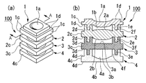
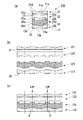
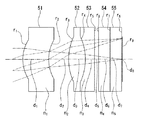
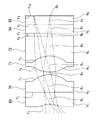
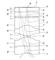
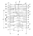
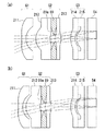
まず本発明に係る第1の実施形態の撮像レンズユニットについて説明する。図1(a)は、本実施形態に係る撮像レンズユニット100を説明するための概略斜視図である。図1(b)は、図1(a)のA−A断面図である。
【0026】
撮像レンズユニット100は3つのレンズ1、2、4および光学フィルター4を有する。3つのレンズ1、2、4をそれぞれの光軸を合わせた状態で光軸方向に重ねられている。そして、レンズ2とレンズ4の間に、光学素子としてパワーを有していないフィルター面を備える光学フィルター3(光学フィルター部材)を挟む構成になっている。それぞれの光学素子は、光軸方向に隣接された光学素子同士が接合されることにより一体化されている。
【0027】
レンズ1は、凹面からなるレンズ面1aと凸面からなるレンズ面1bを中央部に備え、その外周部にはレンズ面1a、1bの光軸に直交する方向に延びるフランジ部1dが設けられている。フランジ部1dの外周は、平面視でほぼ正方形状に形成され、光軸とほぼ平行な4つのフランジ側面1c(側面)を備えている。また、フランジ部1dのレンズ2側の面上には、矩形断面を有する円筒状の位置決め突起1eが複数設けられている。
【0028】
レンズ2、光学フィルター3およびレンズ4は、レンズ1と同様に、フランジ部2d、3dおよび4dを備えている。また、各々4つのフランジ側面2c、3cおよび4c(側面)を備えている。同一方向に配されるフランジ側面1c、2c、3cおよび4cは、それぞれ光軸方向に沿う同一平面中に配置されている(接している)。なお、フランジ部1d、2d、3d、4dの外周部は、重ねて接合された状態で、光軸方向に互いにすきまを形成する形状とされている。
【0029】
また、レンズ2、光学フィルター3およびレンズ4は、光学面として、それぞれ、凸面のレンズ面2a、2b、表面にフィルター処理を施されたフィルター面3a、3b、凹面のレンズ面4aおよび平面のレンズ面4bを備えている。したがって、レンズ1、2は正のパワーを有する正レンズであり、レンズ4は負のパワーを有する負レンズである。
【0030】
また、フランジ部2dのレンズ1側には、位置決め突起1eに嵌合する凹溝から形成された位置決め溝2fが位置決め突起1eの数と同じだけ設けられている。そして、これら位置決め突起1eと位置決め溝2fにより、位置決め部が構成されている。位置決め突起1eと位置決め溝2fは、レンズ1とレンズ2の光軸が一致する位置で、光軸に直交する方向にガタなく嵌合するように、それぞれ形成されている。
また位置決め溝2fの光軸方向の先端面は、フランジ部1dに突き当たるように形成されている。これにより、レンズ面1bとレンズ面2aとの間に空気間隔が設けられた状態で、レンズ1とレンズ2が光軸方向に正確に位置決めされている。この空気間隔は、パワーを有するレンズ面1b、2aで挟まれており、パワーを有する空気レンズとして機能するものである。
【0031】
同様に、フランジ部2dのレンズ3側、フランジ部3dのレンズ2側、レンズ4側、およびフランジ部4dの光学フィルター3側に、それぞれ位置決め部である位置決め突起2e、位置決め溝3f、位置決め突起3e、位置決め溝4fが設けられている。そしてそれぞれの光軸が一致させられ、それぞれの光学面の間に適宜の空気間隔が設けられるように位置決めされている。
【0032】
なお、図1では見易くするために位置決め部の形状の一例を誇張して描いているが、光軸方向、ならびに光軸に直交する方向に、位置を規制できればどのような大きさ、形状であってもかまわない。例えば、互いに嵌合する形状では、図1(b)に示した位置決め突起1eおよび位置決め溝2fの他に、V字突起とV字溝でもよいし、ピンとピン穴でもよく、球と球穴でもよい。また、それぞれの位置決め方向に基準面を有する突起を設け、基準面同士を押し当てて位置決めする構成によってもよい。
【0033】
レンズ1、2、光学フィルター3、レンズ4の接合手段は、適宜の手段が採用できる。例えば、UV硬化樹脂などの接着剤による接着やレーザ溶着などの手段が採用できる。
【0034】
それぞれの光学素子は、ガラスまたは合成樹脂をモールド成形することによって製造することができる。特に、パワーを有する光学素子は、より安定した光学特性を実現し、より小型化を図るために、材料としてガラスを用いるのが好ましい。これは、ガラスは屈折率が大きく面精度に優れ硝材の均一性や温度安定性に優れるからである。
【0035】
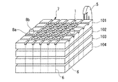
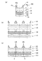
また、撮像レンズユニット100は、次のようにして製作される。まず、レンズ1、レンズ2、光学フィルター3およびレンズ4を、同一ピッチで2次元格子状に配列したアレイ101、102、103、104(光学素子アレイ)として製作する。このとき、位置決め突起と位置決め溝も形成しておく。次に、それぞれのアレイを光軸を一致させて位置決めして接合する。そして、図2に示すように、その状態で切断線6に沿ってカッター5などの切断手段で切断する。この場合、フランジ側面1c、2c、3c、4cは、切断線6に沿った切り口として形成される。よって、フランジ側面1c、2c、3c、4cは、同一面内に配されている(同一面に接している)。この同一面は、光軸に沿う方向に直線状にのびる平面である。本例の場合、この同一面は光軸に平行であるが、切断の仕方によっては光軸と非平行になる場合もある。なお、必要に応じて、切断後、ラップ処理などによって、それぞれのフランジ側面1c、2c、3c、4cに面仕上げを施してもよい。
【0036】
なお、各アレイ101、102、103、104の、光軸に直交する方向の位置決めは、少なくとも2箇所の位置決め孔8aを設け、それらに位置決めピン8bを貫通させることにより行うことができる。また例えば、各アレイ101、102、103、104を光軸に直交する方向に移動可能に保持する製造治具を用いて行ってもよい。
【0037】
なお、上記に説明した撮像レンズユニット100で、光学面を除く面、すなわちフランジ部1d、2d、3d、4dやフランジ側面1c、2c、3c、4cには、塗装や蒸着などの手段により、光吸収性部材を設ける処理を施すことが好ましい。特に、そのような処理は、フランジ側面1c、2c、3c、4cでは、光吸収性を有する薄膜部材をそれらの面に巻きつけて固定して行ってもよい。その場合、例えば、ゴム・熱収縮チューブなどの収縮性薄膜部材をかぶせて固定してもよい。また、紙や合成樹脂などからなる非収縮性薄膜部材を接着材や粘着材などによりフランジ側面1c、2c、3c、4cに巻きつけて固定してもよい。
【0038】
次に、本実施形態に係る撮像レンズユニット100の作用について説明する。本実施形態に係る撮像レンズユニット100によれば、レンズ1、2、4、光学フィルター3などの光学素子が、光軸方向に隣接する光学素子同士で位置決めされて接合されているので、光学素子を取り付けて保持する鏡枠部材などの別部材が不要である。その結果、部品点数が削減できて製造コストを低減することができ、合わせて軽量化、小型化を図ることができる利点がある。
【0039】
また、本実施形態によれば、光軸方向の位置決め部が光学面の外周部をなすフランジ部1d、2d、3d、4d上に一体に設けられているので、部品積み上げ誤差が減り、高精度に空気間隔を設けることができる。また、空気界面を備える屈折面は屈折率差が少ない接合レンズ面に比べてパワーが大きいから、空気間隔を大きくすることによって、空気間隔が狭い場合(空気間隔がない場合も含む)に比べて、同じ数の光学素子でより高い性能が得られる。
【0040】
また本実施形態では、光学素子を光学面の外周部にフランジ部1d、2d、3d、4dを設けているので、フランジ部1d、2d、3d、4dに位置決め部を形成することができる。またこのフランジ部を接合面に利用できる。よって、光学面を傷つけたり汚したりする恐れがなくなるから、製作の効率が向上するという利点がある。
また、フランジ部1d、2d、3d、4dの外周部には外側に向かって突起部が形成されている。この突起部は他の光学素子を重ねた時に、光軸方向にすきまが形成される形状になっている。このようにすれば、このすきまを接着剤のにげ部や、切断時の切りくずのにげ部として利用できる。
【0041】
以上に述べたように、本実施形態に係る撮像レンズユニット100は、各光学素子の外周部のフランジ部1d、2d、3d、4dに、光軸にほぼ平行な4角柱面に整列するフランジ側面1c、2c、3c、4cを備える。よって、このフランジ面の一面を、取り付け面として利用することができる。また、上記に説明したように、本実施形態に係る撮像レンズユニット100は、光学素子アレイを重ねて接合してからカッター5で切断して製作されたものである。そのように製作すれば、多数の光学素子を含む光学素子アレイ同士をまとめて位置決めして、接合してその位置関係を固定できる。よって、個々の光学素子を位置決めして個々に接合する場合に比べて、格段に生産性を向上することができるという利点がある。このような利点は、各光学素子が小さい場合には、一層顕著であり、小型の撮像レンズユニットの大量生産に好適である。
【0042】
なお、上記の説明では、パワーを有する光学素子が3枚である例を説明したが、その枚数を増やしてより光学性能を向上させる構成としてもよいことは言うまでもない。その際、正レンズと負レンズをそれぞれ少なくとも1枚ずつ備えることにより、収差補正を行うことが可能となる。
また、パワーを有する光学素子の重ね枚数は、10枚以下であることが好ましい。そのように構成すれば、位置決め部の加工誤差や光学素子の組立誤差などによって芯ずれ誤差が累積し過ぎることを防ぐことができる。また、パワーを有する光学素子の重ね枚数は、8枚以下とすれば、より好ましく、7枚以下とすれば、さらに一層好ましい。光学素子の重ね枚数は、撮像レンズユニット100に必要な性能と製作コストとの関係から総合的に決めることができる。
【0043】
また、上記の説明では、空気間隔の大きさについては、特に制限していないが、空気間隔の大きさに限度を設けるのが好ましい。空気間隔を適度の大きさに留めておけば、位置決め部の光軸方向長さが短くなり、寸法精度のよい加工が容易となる。その結果、組立時に芯ずれ誤差を防止できる。
具体的には、TDを前記光学素子が接合されて構成される光学系の第1面から最終面までの光軸上の面間隔(光学系の全長)、STを光軸上における空気間隔の長さの総和(空気間隔和)、MTを光軸上における空気間隔の長さの最大値(最大空気間隔)と定義したときに、撮像レンズユニットが、次式を同時に満たすことが好ましい。
ST/TD<0.7 (1)
MT/TD<0.5 (2)
上記各式の上限をうわまわると、空気間隔あるいは光学系の全長が長くなるので芯ずれが大きくなる。その結果、十分な光学性能を得るのが難しくなる。
また、光学素子の組立・加工精度をより向上するためには、式(1)、(2)に代えて、以下の式(3)、(4)を満たすことが好ましい。
ST/TD<0.6 (3)
MT/TD<0.4 (4)
光学素子の組立・加工精度をさらに向上させるためには、式(1)、(2)に代えて、以下の式(5)、(6)を満たすことが好ましい。
ST/TD<0.5 (5)
MT/TD<0.3 (6)
【0044】
さらに、上記の説明では、光学素子の空気界面の枚数は8枚の例で説明したが、空気界面の枚数に限度を設けた構成としてもよい。そうすれば、空気界面において発生しやすい迷光を低減できる。その結果、ゴーストやフレアの発生を防止して、画質を向上することができる。また、反射防止コート処理を施す必要のある光学面をなくすか、少なくすることができ、低コスト化が可能となる。
そのため、空気界面の枚数を10枚より少ない枚数に制限することが好ましい。より迷光が低減するためには、空気界面の枚数は8枚より少ないことがより好ましく、6枚より少ないことがさらに好ましい。
【0045】
また、上記の説明では、光学面の形状に特に制限を設けない例で説明したが、光学素子の曲面形状を制限して傾斜を緩やかにすることが好ましい。これにより、フォームタリサーフなどの接触型形状測定装置での測定が可能となる。接触型形状測定装置を使用することにより、直接的に形状誤差を知ることができる。よって、光学特性を測定することなく部品の良否判定ができる。また、測定結果を製造過程にフィードバックすることで、製造過程の改良ができる。また、迅速な光学面の形状測定ができる。その結果、本実施形態に係るパワーを有する光学面の製作の効率を向上させることができるという利点がある。
具体的には、傾斜角θを、光学素子の光学面における光軸と光学面の法線のなす角と定義したときに、光学素子の各光学面の傾斜角θを、その最大値が60度より小さくすることが好ましい。また、傾斜角θの最大値を55度より小さくすれば、形状誤差が大きい場合でもより測定精度が上げることができるから、精度のよい光学面の製作が容易となって好ましい。さらに、傾斜角θの最大値を50度より小さくすれば、より好ましい。
【0046】
次に、本実施形態のいくつかの変形例について説明する。いずれも上記に説明した実施形態と異なる点を中心に説明する。また変形例の説明においては、上述した第1の実施形態の説明と共通する部材には同一の符号を付して、説明を省略する。
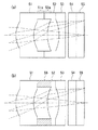
まず第1の変形例について説明する。図3(a)は、本実施形態の第1変形例を説明するための斜視説明図である。図3(b)は、図3(b)のB−B断面図である。図3(c)、(d)は、第1変形例の製造方法の一例を説明するための光軸方向断面の概念図である。
【0047】
図3(a)、(b)に示したように、本変形例に係る撮像レンズユニット110は、レンズ11、12、13を備えている。それらはそれぞれ光軸が一致させられ、それぞれ光軸に直交する方向に延びるフランジ部11d、12d、13dにより、順次重ねられて接合されている。図1の撮像レンズユニット100とは異なり、フランジ部11d、12d、13dには、位置決め突起や位置決め溝が設けられていない。それらフランジ部は、平面視でほぼ正方形とされ、それぞれ光軸とほぼ平行な4つの平面に整列されたフランジ側面11c、12c、13c(側面)を備える。同一方向に配されるフランジ側面11c、12c、13cは、図3(a)に示したように、それぞれ光軸方向に沿う同一平面中に配置されている。
【0048】
レンズ11は、凸面からなるレンズ面11aと凹面からなるレンズ面11bを備える正レンズである。レンズ12は、凸面からなるレンズ面12a、12bを備える正レンズである。レンズ13は、凹面からなるレンズ面13aと平面のレンズ面13bからなる負レンズである。
【0049】
レンズ面11b側のフランジ部11dと、レンズ面12a側のフランジ部12dとは、それらが互いに当接している。但し、レンズ面11bとレンズ面12aの曲率半径が異なるので、レンズ面11b、12aとの間に空気間隔が形成されている。
また、レンズ面12bとレンズ面13aとは、同一の曲率半径を備え、それらの間にレンズ接着用接着剤を介して接合されている。その際、接合面であるレンズ面12b、13aのパワーφは、撮像レンズユニット110の全光学系のパワーをφAとしたときに、
0<|φ/φA|<0.5 (7)
を満たすようにする。ここで、|a|は、aの絶対値を示す。
【0050】
本変形例では、撮像レンズユニット100の場合とは異なり、各光学素子の光軸に直交する方向の位置決め部を備えていない。そこで、レンズ11、12、13単体から撮像レンズユニット110を製作する場合は、光軸に直交する方向の位置決めは、適宜の治具により各光学素子を把持して、各光学素子の光軸が一致する位置に移動させることにより行う。または、各光学素子のフランジ側面11c、12c、13cを光軸からの距離が精度よく揃うように製作し、フランジ側面11c、12c、13cを適宜の基準面に整列させることにより、行ってもよい。また、単体から製作するのではなく、図3(c)、(d)に示したように、レンズ面11a、11b、12a、12b、13a、13bが配列されたアレイ111、112、113(光学素子アレイ)を製作し、各光学素子アレイを動かして位置決めを行い、接合してから切断する製造方法をとってもよい。なお、図3(c)、(d)は、この方法を本変形例に適用した場合の製造工程の概念図である。接合や切断の手段は、すでに第1の実施形態に説明したのと同様の手段を用いることができる。
【0051】
本変形例によれば、3つの光学素子を備え、その内の1組が光学面を接合された接合レンズとされている。そのため、接合された光学素子の屈折率をそれぞれ適宜選定することにより色収差の補正を行うことができる。その結果、色収差が少ない高性能の撮像レンズユニットとすることができる。
【0052】
また、この接合面におけるパワーφが式(7)を満たすように構成するから、接合面の曲率半径を過度に小さくしなくともよいので、接合面の加工が容易となる。その結果、接合面に用いる光学面を安価に製作することができる。
なお、本変形例では接合レンズが1組の例であったが、色収差をさらに向上するために、接合面の数を増やしてもよい。その場合、式(7)におけるφは、それら接合面のパワーの最大値と読み替えるものとする。
【0053】
また、接合面の加工性をより向上させるには、曲率半径が大きくなるように、式(7)に代えて下式を満足させることが好ましい。
0<|φ/φA|<0.4 (8)
さらに接合面の加工性を向上させるには、式(7)に代えて下式を満足させることが好ましい。
0<|φ/φA|<0.3 (9)
【0054】
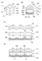
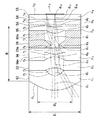
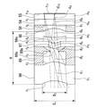
次に、第2の変形例について説明する。図4(a)は、本実施形態の第2変形例を説明するための光軸方向の断面図である。図4(b)、(c)は、第2変形例の製造方法の一例を説明するための光軸方向断面の概念図である。
図4(a)に示したように、本変形例に係る撮像レンズユニット120は、4枚の光学素子としてレンズ21、22、24、13を備え、レンズ22、24の間に、光束を所定の形状に規制する開口絞り23(挟持部材)が設けられている。それぞれの光学素子には、フランジ側面21c、22c、24c、13c(側面)を備えている。同一方向に配されるフランジ側面21c、22c、24c、13cは、それぞれ光軸方向に沿う同一平面中に配置されている。
【0055】
レンズ21、22は、それぞれ平凹、平凸レンズであり、それぞれの平面のレンズ面21b、22aで接合されている。レンズ22は、凸面のレンズ面22b側のフランジ部22d上には、光軸方向に突出された位置決め突起22eが設けられている。
【0056】
開口絞り23は、表面が光吸収性とされた合成樹脂、金属などからなり、光学素子のフランジ側面21c、22c、24c、13cが整列する平面に揃う端面を備えている。
レンズ24は、両凸の正レンズで、レンズ面24bがレンズ面13aの凹面と接合されている。レンズ面24aの側のフランジ部24dには、光軸方向に突出された位置決め突起24eが設けられている。
位置決め突起22e、24eはそれぞれ対向され、開口絞り23を挟持した状態で接合されている。そして、レンズ面22b、24aの間には空気間隔が形成されている。
【0057】
このような撮像レンズユニット120は、図4(b)、(c)に示したように、レンズ面21a、21b、22a、22b、24a、24bが配列されたアレイ121、122、124(光学素子アレイ)とアレイ113とを重ねて接合してから切断する方法によって製造することができる。その際、各光学素子の配列ピッチに一致させた開口部を設けた開口絞りシート123を、アレイ122、124の間に挟んで接合することにより、切断後に開口絞り23が形成される。なお、開口絞りシート123の素材としては、合成樹脂や、金属が用いられる。
【0058】
本変形例によれば、対向する位置決め突起22e、24eによって、レンズ面22bとレンズ面24bとの間に所定の空気間隔を形成することができる。また、フランジ部で接合しているので、光学素子を一体化したときの形状を簡素にすることができる。その結果、光学素子の成形性が向上し、成形精度を確保しつつ生産性を向上させることができるという利点がある。
また、本変形例によれば、撮像レンズユニット120内に開口絞り23を一体化できる。この場合、開口絞りシート123を用いて製造すれば、位置合わせと接合が光学素子アレイと同様の工程によってできるので、容易かつ高精度に組み立てることができるという利点がある。
【0059】
次に、第3の変形例について説明する。図5(a)は、本実施形態の第3変形例を説明するための光軸方向の断面図である。図5(b)、(c)は、第3変形例の製造方法の一例を説明するための光軸方向断面の概念図である。
図5(a)に示したように、本変形例に係る撮像レンズユニット130は、第2変形例と同じ構成のレンズ21、22、24、13を備え、同一方向に配されるフランジ側面21c、22c、24c、13cは、それぞれ光軸方向に沿う同一平面中に配置されている。
【0060】
ただし、レンズ21のレンズ面21bには、遮光膜として、開口絞りコート31が形成されている。この開口絞りコート31により所定の大きさの光束がレンズ21に入射する。また、レンズ13のレンズ面13bには、遮光膜として、フレア絞りコート32が形成されている。このフレア絞りコート32により、有効レンズ径以外の部分から光が入射するのを防止することができる。すなわち、フレア絞りコート32はフレア防止機能を備える。
【0061】
開口絞りコート31、フレア絞りコート32はいずれも、光吸収性材料による塗装や蒸着などにより形成することができる。光学素子アレイを用いて製造する場合には、図5(b)、(c)に示したように、アレイ121、113のそれぞれに開口絞りコート31、フレア絞りコート32を形成してから、重ねて接合する。
【0062】
本変形例によれば、開口絞りコート31、フレア絞りコート32がそれぞれ光学素子に形成されているので、別部材で絞りを設ける必要がない。そのため、接合に際して位置合わせをする手間が省けるとともに、部品点数が削減できる。その結果、生産性を向上させることができ、製造コストを低減できる。
【0063】
次に、第4の変形例について説明する。図6(a)は、本実施形態の第4変形例を説明するための光軸方向の断面図である。図6(b)、(c)は、第4変形例の製造方法の一例を説明するための光軸方向断面の概念図である。
図6(a)に示したように、本変形例に係る撮像レンズユニット140は、第2変形例と同じ構成のレンズ21、22、24、13を備えている。同一方向に配されるフランジ側面21c、22c、24c、13cは、それぞれ光軸方向に沿う同一平面中に配置されている。
【0064】
本変形例では、レンズ21にフード部材41が接合されている。
フード部材41は、少なくとも表面が光吸収性とされた合成樹脂などからなる。フード部材41は、傾斜した内面41aを有する壁体である。内面41aは、レンズ21の有効レンズ径を取り囲んで光軸方向に拡径されながら延びている。このような構造により、フード部材41は、レンズ21に入射する外光を規制する機能を有する。外周面41cは、フランジ側面21c、22c、24c、13cに整列されている。
本変形例においても、フード部材41がアレイ状に形成されたフードアレイ部材141を製作して、光学素子アレイとともに重ねて接合してから、切断する製造方法が採用できる。
【0065】
本変形例によれば、フード部材41を各光学素子と一体に接合するので、外光が入射しにくく画質が向上された撮像レンズユニットを容易、安価に製作することができる。
【0066】
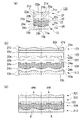
次に第5の変形例について説明する。図7(a)は、本実施形態の第5変形例を説明するための光軸方向の断面図である。図7(b)、(c)は、第5変形例の製造方法の一例を説明するための光軸方向断面の概念図である。
図7(a)に示したように、本変形例に係る撮像レンズユニット145は、第2変形例に係る撮像レンズユニット120のレンズ22に代えて、集光レンズ25を備えている。
【0067】
レンズ25は、レンズ面25a、25b(光学面)を備え、レンズ21、開口絞り23と、フランジ部25d、位置決め突起25eとの間でそれぞれ接合されている。レンズ面25bとレンズ面24aとの間には空気間隔が形成されている。フランジ面25c(側面)は、フランジ面21c、24c、13cと光軸方向に沿う同一平面中に配置されている。
レンズ25は、レンズ22から硝材の屈折率やレンズ面25a、25bの形状を適宜変えて、フランジ部25dと位置決め突起25eとの間の寸法が小さくなるように設計されたレンズである。具体的には、レンズ22に対して、例えば、屈折率が大きい硝材に変えたり、レンズ面25a、25bのいずれかを非球面としたりすることにより設計することができる。
【0068】
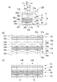
このような撮像レンズユニット145は、光軸に沿う方向の切断長さの合計を距離TTと定義するときに(本変形例では、図7(a)の距離H、すなわち、レンズ面21a側のフランジ面21dからレンズ面13b側のフランジ面13dまでの長さ)、次の関係を満足させる。
TT<20mm (10)
【0069】
また、撮像レンズユニット145の最大外径、すなわち光軸を中心軸として撮像レンズユニット145を含む仮想円筒のうち最小の円筒径、をMD、撮像レンズユニット145の最大光線有効直径をEDと定義するときに、次の関係を満足させる。
1.0<MD/ED<4.0 (11)
本変形例では、撮像レンズユニット145は、正4角柱に切断されており、図7(a)には、光軸を挟んで対向する光軸方向の角柱稜線を含む断面を示している。したがって、図中のD1は、正4角柱の外接円筒の直径となっており、上記のMDとなっている。図中のD2は、レンズ面21aの最大光線有効直径であり、上記のEDとなっている。
【0070】
本変形例によれば、距離TTが式(10)を満足するようにするので、撮像レンズユニット145を、アレイ121、125、開口絞りシート123、アレイ124、113を重ねて接合してから切断して製造する際、比較的短時間に切断できる合理的な切断厚みとすることができる。その結果、生産性を向上することができるという利点がある。しかも切断による発熱量も低減されるので、熱歪の発生などによる光学性能の劣化を防止することができるという利点がある。
また、より短時間に切断して生産性を向上するためには、距離TTをより小さな値とすることが望ましい。そこで、
TT<15mm (12)
の関係を満足することが好ましい。さらには、
TT<10mm (13)
の関係を満足することが好ましい。
【0071】
また、本変形例によれば、MD/EDが式(11)を満足するようにするので、光束が通過しない部分の大きさを合理的な範囲とし、製造上合理的な数の光学素子を光学アレイ素子上に配列することができる。その結果、切断工数当たりの撮像レンズユニットの製造個数を増大することができ、生産性を向上することができるという利点がある。
また、光学素子アレイ当たりの撮像レンズユニットの取り数をさらに増やして生産性をより向上するためには、MD/EDをより小さな値とすることが望ましい。そこで、
1.0<MD/ED<3.0 (14)
の関係を満足することが好ましい。さらには、
1.0<MD/ED<2.0 (15)
の関係を満足することが好ましい。
【0072】
なお、上記の第5変形例の説明では、レンズ25の厚みを低減して距離TTを式(10)の範囲に収める例で説明したが、距離TTが式(10)の範囲に収められれば、どの光学素子を薄くしてもよいことは言うまでもない。
また、距離TTは、本変形例では、接合部分の厚みと等しくなっているが、距離TTは、実際に切断される合計長さであればよい。例えば、図1に示した例では、切断部と接合部とが別で、切断部は接合部より短くなっている。また、図2に示した例では、切断線6上にガイド溝7が設けられ切断部の厚みが低減されている。
【0073】
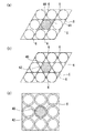
なお、以上に説明した第1の実施形態では、光学素子の側面が、ほぼ正方形断面の4角柱面に整列される例で説明したが、そのような角柱面に限るものではない。撮像レンズユニットの製造上の理由や組付・搬送などの取り扱いの都合によって他の種々の形状を採用できる。
【0074】
例えば、製造上は直線状加工が容易である。よって、特に光学素子アレイから切り出す場合に、工程数が少なくなるので、この加工法を用いれば生産効率がよい。また、加工に際して、撮像レンズユニットの外形は、正方形断面である必要はなく、例えば、図8(a)に示したようにひし形断面の4角柱面でもよい。この場合、正方形断面の場合とは異なり、光学面40を切断可能に最密に並べたとき、光学面40の互いの外周部が接しないので、光学面が精度よく成形できる利点がある。また図8(b)に示したのは、6角形断面の例である。この場合、フランジ部41が小さいため軽量の撮像レンズユニットとすることができるという利点がある。
【0075】
また、特に、レーザおよびウォータージェットなどを使った切断工法を用いれば、光軸に沿う方向に直線状に延びる平面・曲面が容易に形成できるので、図8(c)に示したように円断面で切り出してもよい。このような円筒面に整列した撮像レンズユニットは、整列面を取り付けの受け基準面に用いる場合に、光軸周りに方向性がないので取り付けがきわめて容易となる。
【0076】
また、上記の説明では、光学素子の側面が、光軸にほぼ平行な例で説明したが、光軸に対して傾斜していてもよい。例えば、切断時の加工誤差で傾斜が生じてもよいし、所定の錘面に整列させるために傾斜を設けてもよい。
【0077】
また、上記の説明では、各光学素子は、側面としてフランジ部1d、2d、3d、4d、11d、12d、13d、21d、22d、24d、25dに設けられたフランジ側面1c、2c、3c、4c、11c、12c、13c、21c、22c、24c、25c、152cを備える例で説明したが、光学素子の側面は、光学素子のコバ面からなるものであってもよい。
【0078】
また、上記の説明では、製造に好都合な例として、光学素子の側面が整列する例で説明した。但し、単に鏡枠部材を省略した撮像レンズユニットを構成するという目的を達成するためには、光学素子の側面が整列していなくてもよい。それは、各光学素子は、フランジ部1d、2d、3d、4d、11d、12d、13d、21d、22d、24d、25dの光軸方向の面で接合することができるからである。
【0079】
また、上記の説明では、光学素子アレイとして2次元配列の例を図示して説明したが、1次元配列であってもよいことは言うまでもない。
また、光学素子アレイから切り出して製造する場合、配列方向に複数の光学素子を切り出して、複数の平行光軸を有する撮像レンズユニットとしてもよい。その際、配列方向の複数の光学素子は、光学面の種類が異なるものであってもよい。
【0080】
以上に説明した第1の実施形態に係る撮像レンズユニットに用いることができる光学系の具体的な数値実施例を以下に説明する。
なお、以下では、各実施例に共通して、記号ωは対角全画角、Fは有効Fナンバー、Soは物点距離、IHは像高を表す。また、ST/TD、MT/TD、傾斜角θ、|φ/φA|、TT、MD/EDと表した量は、上記の説明の中で用いたのと同じ名称・定義である。
また後述する数値データの表において、rは曲率半径、dは面間隔、ndは屈折率、νdはアッベ数を表す。ri、di、ni、νi(iは整数)は、曲率半径、面間隔、屈折率、アッベ数である。後述する各光路図には、数値データの表のri、di、niとの対応が示されている。
【0081】
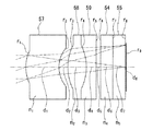
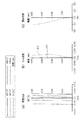
[実施例1]
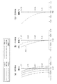
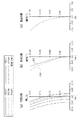
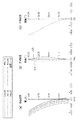
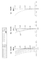
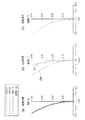
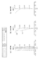
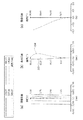
図9に示したのは、第1の数値実施例の光路図である。図10は、本実施例の収差図である。図10(a)は、波長656.27nm、587.56nm、546.07nm、486.13nm、435.84nmに対して計算された球面収差を、横軸に球面収差(単位mm)、縦軸に開口比をとって表した収差図である。図10(b)は、横軸に非点収差(単位mm)、縦軸に画角(単位°)をとって表した収差図である。ΔMはメリディオリナル像面のずれ量、ΔSはサジタル像面のずれ量を表す。図10(c)は、横軸に歪曲収差(単位%)、縦軸に画角(単位°)をとって表した収差図である。
【0082】
本実施例の構成は、物体側から順に、正パワーを有する第1レンズ51、正パワーを有する第2レンズ52、負パワーを有する第3レンズ53およびフィルター部材54、55を備えている。第1レンズ51と第2レンズ52との間には空気間隔が設けられている。第2レンズ52と第3レンズ53とは光学面同士が接合されている。なお、図示していないが、第1レンズ51の像側面には蒸着によって絞りが形成されている。
第1レンズ51と第2レンズ52との空気間隔は、図11(a)に示したように、第1レンズ51と第2レンズ52にそれぞれ位置決め突起51a、52aを設けてそれぞれを光軸方向に当接させてもよいし、図11(b)に示したように、第1レンズ51と第2レンズ52の間にスペーサ56(挟持部材)を挟んでよい。
なお、以下に説明する、他の数値実施例の空気間隔はすべて、上記いずれかの手段によって形成することができる。
【0083】
本実施例は、物点距離So=960mmとして、過焦点距離に設定している。対角全画角は、ω=40°、有効Fナンバーは、F2.8、像高は、IH=0.924mmである。
また、空気界面は6枚、ST/TD=0.42、MT/TD=0.20、傾斜角θは33°、|φ/φA|=0.08である。
第1レンズ51と第2レンズ52の間に空気間隔を設けることで、像面湾曲の補正を行っている。
【0084】

図10から分かるように、本実施例の撮像レンズユニットは、可視光域で良好な収差特性を有するものとなっている。
【0086】
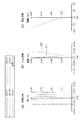
[実施例2]
図12に示したのは、第2の数値実施例の光路図である。図13は、本実施例の収差図である。図13(a)、(b)、(c)は、それぞれ図10(a)、(b)、(c)で説明したグラフと同様に描かれているので、そのグラフ軸などの説明は省略する。
【0087】
本実施例の構成は、物体側から順に、正パワーを有する第1レンズ57、正パワーを有する第2レンズ58、負パワーを有する第3レンズ59およびフィルター部材54、55を備えている。第1レンズ57と第2レンズ58との間には空気間隔が設けられている。第2レンズ58と第3レンズ59とは光学面同士が接合されている。なお、図示していないが、第1レンズ57の物体側面には蒸着によって絞りが形成されている。
【0088】
本実施例は、物点距離So=960mmとして、過焦点距離に設定している。対角全画角はω=40°、有効FナンバーはF2.8、像高はIH=0.924mmである。
また、空気界面は6枚、ST/TD=0.14、MT/TD=0.09、傾斜角θは37°、|φ/φA|=0.09である。
第1レンズ57と第2レンズ58との間に空気間隔を設けることで、像面湾曲の補正を行っている。
【0089】
図13から分かるように、本実施例の撮像レンズユニットは、可視光域で良好な収差特性を有するものとなっている。
【0091】
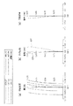
[実施例3]
図14に示したのは、第3の数値実施例の光路図である。図15は、本実施例の収差図である。図15(a)、(b)、(c)は、それぞれ図10(a)、(b)、(c)で説明したグラフと同様に描かれているので、そのグラフ軸などの説明は省略する。
【0092】
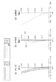
本実施例の構成は、物体側から順に、負パワーを有する第1レンズ60、正パワーを有する第2レンズ61、正パワーを有する第3レンズ62、負パワーを有する第4レンズ63およびフィルター部材54、55を備えている。第1レンズ60および第2レンズ61、ならびに第3レンズ62および第4レンズ63はそれぞれ光学面同士が接合されている。第2レンズ61と第3レンズ62との間には空気間隔が設けられている。なお、図示していないが、第1レンズ60の像側面には蒸着によって絞りが形成されている。
【0093】
本実施例は、物点距離はSo=10mm、対角全画角はω=90°、有効FナンバーはF3.0、像高はIH=0.924mmである。
また、空気界面は6枚、ST/TD=0.07、MT/TD=0.04、傾斜角θは46°、|φ/φA|=0.07である。
第2レンズ61と第3レンズ62との間に空気間隔を設けることで、像面湾曲の補正を行っている。
【0094】
図15から分かるように、本実施例の撮像レンズユニットは、可視光域で良好な収差特性を有するものとなっている。特に、図15(a)を見ると、接合レンズを2組使用しているため、第1、2実施例と比較して色収差が良好に補正されていることが分かる。さらに図15(b)に示したように、非点収差もきわめて良好に補正されている。
【0096】
[実施例4]
図16に示したのは、第4の数値実施例の光路図である。図17は、本実施例の収差図である。図17(a)、(b)、(c)は、それぞれ図10(a)、(b)、(c)で説明したグラフと同様に描かれているので、そのグラフ軸などの説明は省略する。
【0097】
本実施例の構成は、物体側から順に、負パワーを有する第1レンズ65、正パワーを有する第2レンズ66、正パワーを有する第3レンズ67、負パワーを有する第4レンズ68およびフィルター部材54、55を備えている。第1レンズ65および第2レンズ66、ならびに第3レンズ67および第4レンズ68はそれぞれ光学面同士が接合されている。第2レンズ66と第3レンズ67との間には空気間隔が設けられている。なお、図示していないが、第1レンズ65の物体側面には蒸着によって絞りが形成されている。
【0098】
本実施例は、物点距離はSo=10mm、対角全画角はω=90°、有効FナンバーはF3.0、像高はIH=0.924mmである。
また、空気界面は4枚、ST/TD=0.09、MT/TD=0.04、傾斜角θは45°、|φ/φA|=0.04である。
第2レンズ61と第3レンズ62との間に、空気間隔を設けることで、像面湾曲の補正を行っている。
【0099】
図17から分かるように、本実施例の撮像レンズユニットは、可視光域で良好な収差特性を有するものとなっている。特に、図17(a)を見ると、接合レンズを2組使用しているため、第1、2実施例と比較して色収差が良好に補正されていることが分かる。さらに図17(b)に示したように、非点収差もきわめて良好に補正されている。
【0101】
[実施例5]
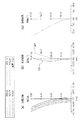
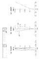
図18に示したのは、第5の数値実施例の光路図である。図19は、本実施例の収差図である。図19(a)、(b)、(c)は、それぞれ図10(a)、(b)、(c)で説明したグラフと同様に描かれているので、そのグラフ軸などの説明は省略する。
【0102】
本実施例の構成は、物体側から順に、負パワーを有する第1レンズ69、正パワーを有する第2レンズ70、正パワーを有する第3レンズ71、負パワーを有する第4レンズ72およびフィルター部材54、55を備えている。第1レンズ69および第2レンズ70、ならびに第3レンズ71および第4レンズ72はそれぞれ光学面同士が接合されている。第2レンズ66と第3レンズ67との間には空気間隔が設けられている。なお、図示していないが、第1レンズ69の像側面には蒸着によって絞りが形成されている。
【0103】
本実施例は、物点距離はSo=10mm、対角全画角はω=90°、有効FナンバーはF3.0、像高はIH=0.924mmである。
また、空気界面は6枚、ST/TD=0.07、MT/TD=0.03、傾斜角θは41°、|φ/φA|=0.06である。
第2レンズ61と第3レンズ62との間に空気間隔を設けることで、像面湾曲の補正を行っている。
【0104】
図19から分かるように、本実施例の撮像レンズユニットは、可視光域で良好な収差特性を有するものとなっている。特に、図19(a)を見ると、接合レンズを2組使用しているため、第1、2実施例と比較して色収差が良好に補正されていることが分かる。さらに図19(b)に示したように、非点収差もきわめて良好に補正されている。
【0106】
[実施例6]
図20に示したのは、第6の数値実施例の光路図である。図21は、本実施例の収差図である。図21(a)、(b)、(c)は、それぞれ図10(a)、(b)、(c)で説明したグラフと同様に描かれているので、そのグラフ軸などの説明は省略する。
【0107】
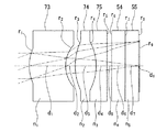
本実施例の構成は、物体側から順に、正パワーを有する第1レンズ73、正パワーを有する第2レンズ74、負パワーを有する第3レンズ75およびフィルター部材54、55を備えている。第2レンズ74と第3レンズ75とは光学面同士が接合されている。第1レンズ73と第2レンズ75との間には空気間隔が設けられている。なお、図示していないが、第1レンズ73の物体側面には蒸着によって絞りが形成されている。
【0108】
本実施例では、第3レンズ75にポリカーボネート樹脂を使用している。
本実施例は、物点距離So=960mmとして、過焦点距離に設定している。対角全画角はω=40°、有効FナンバーはF2.8、像高はIH=0.924mmである。
また、空気界面は6枚、ST/TD=0.14、MT/TD=0.09、傾斜角θは38°、|φ/φA|=0.20である。
第1レンズ73と第2レンズ74との間に空気間隔を設けることで、像面湾曲の補正を行っている。
【0109】
図21から分かるように、本実施例の撮像レンズユニットは、比較的屈折率の小さいポリカーボネート製の合成樹脂レンズを用いているにもかかわらず、可視光域で良好な収差特性を有するものとなっている。このように本実施例では、合成樹脂であるポリカーボネート製のレンズを使用して安価なレンズを製作できるので、低コストな撮像レンズユニットとすることができるという利点を有する。合成樹脂成形を用いると空気間隔を設けるための位置決め突起を容易に設けることができる利点もある。
【0111】
[実施例7]
図22に示したのは、第7の数値実施例の光路図である。図23は、本実施例の収差図である。図23(a)、(b)、(c)は、それぞれ図10(a)、(b)、(c)で説明したグラフと同様に描かれているので、そのグラフ軸などの説明は省略する。
【0112】
本実施例の構成は、物体側から順に、負パワーを有する第1レンズ76、正パワーを有する第2レンズ77、正パワーを有する第3レンズ78、負パワーを有する第4レンズ79およびフィルター部材54、55を備えている。第1レンズ76および第2レンズ77、ならびに第3レンズ78および第4レンズ79はそれぞれ光学面同士が接合されている。第2レンズ77と第3レンズ78との間には空気間隔が設けられている。なお、図示していないが、第1レンズ76の像側面には蒸着によって絞りが形成されている。
【0113】
本実施例では、第3レンズ78には、合成樹脂であるZEONEX(登録商標)を、第4レンズ79には、ポリカーボネート樹脂を使用している。
本実施例は、物点距離はSo=10mm、対角全画角はω=90°、有効FナンバーはF3.0、像高はIH=0.924mmである。
また、空気界面は6枚、ST/TD=0.07、MT/TD=0.03、傾斜角θは46°、|φ/φA|=0.20である。
第2レンズ61と第3レンズ62との間に空気間隔を設けることで、像面湾曲の補正を行っている。
【0114】
図23から分かるように、本実施例の撮像レンズユニットは、屈折率が比較的小さい合成樹脂レンズを2枚使用して構成しているにもかかわらず、可視光域で良好な収差特性を有するものとなっている。特に、図23(a)を見ると、接合レンズを2組使用しているため、第1、2実施例と比較して色収差が良好に補正されていることが分かる。
本実施例によれば、4枚中2枚のレンズに安価な合成樹脂レンズを用いるので、安価な撮像レンズユニットを構成できるという利点がある。
【0116】
[実施例8]
図24示したのは、第8の数値実施例の光路図である。図25は、本実施例の収差図である。図25(a)、(b)、(c)は、それぞれ図10(a)、(b)、(c)で説明したグラフと同様に描かれているので、そのグラフ軸などの説明は省略する。ただし、図25(a)では、波長ごとのデータばらつきが少ないので、波長は656.27nm、587.56nm、486.13nmのみの結果を図示している。
【0117】
本実施例の構成は、物体側から順に、負パワーを有する第1レンズ80、平行平面板81、負パワーを有する第2レンズ82、正パワーを有する第3レンズ83、負パワーを有する第4レンズおよび正パワーを有する第5レンズ85を備えている。第2レンズ82、第3レンズ83、第4レンズ84および第5レンズ85は、それぞれ光学面同士が接合されている。第1レンズ80の凹面(r2)と平行平面板81の物体側面(r3)との間には、空気間隔が形成されている。なお、図示していないが、平行平面板81の像面側面には蒸着によって絞りが形成されている。
本実施例は、物点距離はSo=∞、対角全画角はω=103°、有効FナンバーはF4.3、像高はIH=0.5mmである。
また、空気界面は4枚、ST/TD=0.04、MT/TD=0.03、傾斜角θは45°、|φ/φA|=0.23である。
第1レンズ80と平行平面板81との間に空気間隔を設けることで、像面湾曲の補正を行っている。
【0118】
図25から分かるように、本実施例の撮像レンズユニットは、可視光域で良好な収差特性を有するものとなっている。
本実施例は、パワーを有する第1レンズ80とパワーを有しない平行平面板81との間に空気間隔を設けることによって、空気レンズを形成している例となっている。
【0120】
[実施例9]
図26に示したのは、第9の数値実施例の光路図である。図27は、本実施例の収差図である。図27(a)、(b)、(c)は、それぞれ図10(a)、(b)、(c)で説明したグラフと同様に描かれているので、そのグラフ軸などの説明は省略する。また、図中に示したH、D1、D2は、図7で説明したのと同様の量である。
【0121】
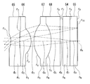
本実施例の構成は、物体側から順に、負パワーを有する第1レンズ87、正パワーを有する第2レンズ88、明るさ絞り89(挟持部材)、正パワーを有する第3レンズ90、正パワーを有する第4レンズ91、スペーサ56およびフィルター部材54、55を備えている。そして、この順に、光軸を合わす必要がある第1レンズ87から第4レンズ91までが、互いに接合されてから正4角柱に切断して製造されている。
第1レンズ87、第4レンズ91には、それぞれ位置決め突起87e、91eが設けられ、第2レンズ88、第3レンズ90との間に空気間隔が形成されている。
明るさ絞り89は、位置決め突起89eを備えて、光学素子間に所定の空気間隔を形成するとともに、光軸方向の中間部に遮光性を有する開口絞り部89aを備える部材である。本実施例では第2レンズ88と第4レンズ91との間の空気間隔を形成し、開口絞り部89aをその中間に配置している。明るさ絞り89は、例えば、合成樹脂成形などにより製造することができる。
スペーサ56は、第4レンズ91とフィルター部材54との間に空気間隔を形成している。
本実施例は、物点距離はSo=260mmとして、過焦点距離に設定している。焦点距離はf=1.47mm、対角全画角はω=66°、有効FナンバーはF2.8、像高はIH=0.924mmである。また、H=TT=5.14mm、D1=4.62mm、D2=2.62である。したがって、MD/ED=D1/D2=1.76である。
【0122】
また非球面は、以下の定義式で与えられる回転対称非球面である。
Z=(y2 /R)/[1+{1−(1+k)y2 /R2 }1/2]+ay4 +by6 +cy8 +dy10+… (16)
ただし、Zを光の進行方向を正とした光軸(軸上主光線)とし、yを光軸と垂直な方向にとる。ここで、
Rは近軸曲率半径、kは円錐定数、a、b、c、d、…はそれぞれ4次、6次、8次、10次の非球面係数である。この定義式のZ軸が回転対称非球面の軸となる。なお、データの記載されていない非球面に関する項は0である。
【0123】
本実施例は、TT、MD/EDが、それぞれ式(13)、式(15)を満足している。その結果、切断の加工性に優れる撮像レンズユニットとなっている。
【0125】
[実施例10]
図28に示したのは、第10の数値実施例の光路図である。図29は、本実施例の収差図である。図29(a)、(b)、(c)は、それぞれ図10(a)、(b)、(c)で説明したグラフと同様に描かれているので、そのグラフ軸などの説明は省略する。また、図中に示したH、D1、D2は、図7で説明したのと同様の量である。
【0126】
本実施例の構成は、物体側から順に、負パワーを有する第1レンズ92、正パワーを有する第2レンズ93、正パワーを有する第3レンズ94、明るさ絞り89、正パワーを有する第4レンズ95、スペーサ56およびフィルター部材54、55を備えている。そして、この順に、光軸を合わす必要がある第1レンズ92から第4レンズ95までが、互いに接合されてから正4角柱に切断して製造されている。
第3レンズ94には、位置決め突起94eが設けられ、第2レンズ93との間に空気間隔が形成されている。
明るさ絞り89は、第3レンズ94と第4レンズ95との間の空気間隔を形成し、開口絞り部89aをその中間に配置している。
スペーサ56は、第4レンズ91とフィルター部材54との間に空気間隔を形成している。
本実施例は、物点距離はSo=340mmとして、過焦点距離に設定している。焦点距離はf=1.67mm、対角全画角はω=60°、有効FナンバーはF2.8、像高はIH=0.924mmである。そして、H=TT=5.80mm、D1=5.42mm、D2=3.62である。したがって、MD/ED=1.50である。なお、下記、非球面式は、実施例9に記載の式(16)である。
【0127】
図29から分かるように、本実施例の撮像レンズユニットは、可視光域で良好な収差特性を有するものとなっている。
本実施例は、TT、MD/EDが、それぞれ式(13)、式(15)を満足している。その結果、切断の加工性に優れるレンズとなっている。
【0129】
[実施例11]
図30に示したのは、第11の数値実施例の光路図である。図31は、本実施例の収差図である。図31(a)、(b)、(c)は、それぞれ図10(a)、(b)、(c)で説明したグラフと同様に描かれているので、そのグラフ軸などの説明は省略する。また、図中に示したH、D1、D2は、図7で説明したのと同様の量である。
【0130】
本実施例の構成は、物体側から順に、負パワーを有する第1レンズ96、明るさ絞り89、正パワーを有する第2レンズ97、正パワーを有する第3レンズ98、スペーサ56およびフィルター部材54、55を備えている。そして、この順に、光軸を合わす必要がある第1レンズ92から第4レンズ95までが、互いに接合されてから正4角柱に切断して製造されている。
明るさ絞り89は、第1レンズ96と第2レンズ97との間の空気間隔を形成し、開口絞り部89aをその中間に配置している。
第3レンズ98には、位置決め突起98eが設けられ、第2レンズ97との間に空気間隔が形成されている。
スペーサ56は、第3レンズ98とフィルター部材54との間に空気間隔を形成している。
本実施例は、物点距離はSo=440mmとして、過焦点距離に設定している。焦点距離はf=1.88mm、対角全画角はω=50°、有効FナンバーはF2.8、像高はIH=0.924mmである。そして、H=TT=4.67mm、D1=3.58mm、D2=2.18mmである。したがって、MD/ED=1.64である。なお、下記、非球面式は、実施例9に記載の式(16)である。
【0131】
図31から分かるように、本実施例の撮像レンズユニットは、可視光域で良好な収差特性を有するものとなっている。
本実施例は、TT、MD/EDが、それぞれ式(13)、式(15)を満足している。その結果、切断の加工性に優れるレンズとなっている。
【0133】
[実施例12]
図32に示したのは、本発明の第1の実施形態に係る撮像レンズユニットを用いて、ズームレンズ光学系を構成した第12の数値実施例の光路図である。図32は、最も広角側(Wと略称する)の光路図である。図33(a)は同じく中間画角(Sと略称する)、図33(b)は同じく最も望遠側(Tと略称する)の光路図である。図33、34、35は、本実施例のそれぞれW、S、Tのレンズ配置における収差図である。図33〜35は、非点収差(各図(b))、歪曲収差(各図(c))の縦軸が像高(単位はmm)で表示されている以外は、それぞれ図10(a)、(b)、(c)で説明したグラフと同様に描かれているので、そのグラフ軸などの説明は省略する。また、図中に示したH1、H2は図7で説明したHと同様の量であり、D2は、図7で説明したのと同様の量である。本実施例は、いずれのレンズ群も正6角柱として切断されており、D1は正6角柱の外接円筒の直径に等しい。
【0134】
本実施例の構成は、物体側から順に、負パワーを有する第1レンズ群G1、正パワーを有する第2レンズ群G2、正パワーを有する第3レンズ群G3、およびフィルター部材54を備えている。そして、第1レンズ群G1と第2レンズ群G2とを移動させることで、約2倍の変倍が可能となっているものである。
第1レンズ群G1は、第1レンズ211からなる。
第2レンズ群G2は、物体側から、凸凹レンズからなる第2レンズ212、明るさ絞り89、両凸レンズからなる第3レンズ213が、この順に互いに接合されてから切断して製造されている。明るさ絞り89により、第2レンズ212と第3レンズ213との間には、空気間隔が形成され、その中間に開口絞り部89aが形成されている。
第3レンズ群G3は、物体側から、凸凹レンズからなる第4レンズ214、凸平レンズからなる第5レンズ215が、第5レンズ215に備えられた位置決め突起215eにより空気間隔を設けて接合されてから切断されている。
【0135】
本実施例は、物点距離はSo=900mmとして、過焦点距離に設定している。焦点距離はf=1.53mm(W)〜2.19mm(S)〜2.99mm(T)、対角全画角はω=31.2°(W)〜22.9°(S)〜17.2°(T)、有効FナンバーはF2.73(W)〜F3.28(S)〜F3.97(T)、像高はIH=0.924mmである。
そして、第2レンズ群G2、第3レンズ群G3のTTであるH1、H2は、H1=2.17、H2=1.30である。また、D1=4.84mm、D2=4.00mmである。したがって、MD/ED=1.21である。なお、下記、非球面式は、実施例9に記載の式(16)である。
また、下記に示す構成パラメータ表において、簡単のため、面間隔は変倍時の値をW〜S〜Tの形で一括して表記している。
【0136】
図34〜36から分かるように、本実施例のズームレンズは、可視光域で良好な収差特性を有するものとなっている。
本実施例は、第2レンズ群、第3レンズ群を形成する撮像レンズユニットのTT、MD/EDが、それぞれ式(13)、式(15)を満足している。その結果、切断の加工性に優れる撮像レンズユニットからなっている。
【0138】
なお、上記の第9〜第11の数値実施例を示した撮像レンズユニットの説明において、光軸を合わす必要のある光学素子、開口絞りなどを接合して切断するとして、TTの長さもそのように計算したが、必要ならば、スペーサなどの他の挟持部材や、光学フィルター部材を接合した状態で切断してもよいことは言うまでもない。その場合でも、上記の第9〜第11の数値実施例は、TTが式(13)を満足する例となっている。
【0139】
[第2の実施形態]
次に、本発明に係る第2の実施形態の撮像装置について説明する。本実施形態の撮像装置は、第1の実施形態に係る撮像レンズユニットを備えているものである。以下、具体的に例を挙げて説明する。
【0140】
図37は、本実施形態に係る撮像装置の一例であるズームレンズ200の光学系の概略構成を示す説明図である。
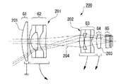
ズームレンズ200は、物体側から、正パワーを有する第1群G1、負パワーを有する第2群G2、正パワーを有する第3群G3、正パワーを有する第4群G4、フィルター部材などを含む第5群G5を備えており、それぞれ不図示の鏡枠に取り付けられ、第2群G2、第3群G3、第4群G4が第1群G1に対して可動に保持されている。
可動とされた第2群G2、第3群G3は、本発明の第1の実施形態に係る撮像レンズユニット201、202によって構成されている。撮像レンズユニット201、202は、それぞれ3枚のレンズが鏡枠を用いることなく、光軸方向に隣接するレンズ間が接合された構成とされている。そして、1つの空気間隔と1つの接合面を有している。
【0141】
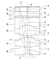
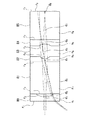
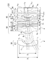
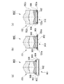
次に、図38は、本実施形態に係る撮像装置に用いられる撮像ユニット900の概略構成を示す光軸方向断面図である。
図38(a)に示したように、撮像ユニット900は、撮像レンズユニット150と撮像素子901を備えている。
この例では、撮像レンズユニット150は3枚のレンズがフランジ部で接合されて一体化されているが、本発明の第1の実施形態に係る撮像レンズユニットはすべて採用することができる。
撮像素子901は、半導体ウエハー上に形成された光電変換デバイスであるCCD902とマイクロレンズ903を有する。そして、CCD902の受光面上にマイクロレンズアレイ903が形成されている。
撮像レンズユニット150とカバーガラス904とは、スペーサ905を介して接着剤906により接着固定されている。
スペーサ905は、例えば、くさび状などの形状を備えることにより、撮像レンズユニット150の、光軸方向の位置および傾きと、カバーガラス904との間隔とをそれぞれ調整することが可能な構成とされている。
【0142】
図38(b)に示したのは、別の撮像ユニット900’の例である。撮像ユニット900’は、撮像レンズユニット150に代えて、別の撮像レンズユニット151を用いたものである。撮像レンズユニット151は、像側最終面に配置された光学素子のフランジ部などに複数の位置決め突起151aを備えている。この位置決め突起51aにより、スペーサ905を省略している。また、撮像ユニット900’は、撮像素子901に代えて、CCD902とマイクロレンズアレイ903を備え、カバーガラス904を有しない撮像素子910を用いて構成した例である。
【0143】
図38(c)に示したのは、さらに別の撮像ユニット900”の例である。撮像ユニット900”は、像側最終面に配置された光学素子のフランジ部などに位置決め突起152aを備えた撮像レンズユニット152と撮像素子910を備えている。そして、CCD902の外周部がフランジ側面152c(側面)に整列された構成を有している。
このような構成は、撮像レンズユニット152を、光学素子アレイを重ねて接合してから切断する方法を用いれば、容易に製作できる。すなわち、接合済みの光学素子アレイを、CCD902がアレイ状に形成された半導体ウエハーに対して位置決めして、位置決め突起152aを接着剤906によって半導体ウエハーに接着し、光学素子アレイと半導体ウエハーを同時に切断することにより製作できる。
【0144】
以下に、撮像ユニット900を用いた本実施形態に係る撮像装置の具体的な例を説明する。
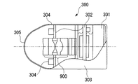
図39に示したのは、撮像ユニット900をカプセル内視鏡300に用いた例である。
カプセル内視鏡300は、照明光源304、撮像ユニット900、撮像ユニット900の撮像素子からの信号を処理する画像処理回路302およびそれらに電源を供給するバッテリー301を備え、全体がカバー303で覆われている。カバー303の先端には、透明窓305が設けられている。この透明窓305を介して、照明光の投射と撮像ユニット900による反射光の受光が行われる。
【0145】
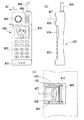
次に、図40に示したのは、撮像ユニット900を携帯用端末400に用いた例である。図40(a)、(b)は、それぞれ正面図、側面図であり、図40(c)は図40(a)のC−C断面図である。
携帯用端末400は、撮像ユニット900が用いられた撮像部405、モニター部404、文字記号や指令信号をボタン・ダイヤルなどで入力する入力部403、マイク部401、スピーカ部402および無線通信の授受を行うアンテナ406を備えている。
図40(c)に示したように、携帯用端末400の内部には、基板取付部410に固定された回路基板409上に、撮像ユニット900に含まれるCCD902が電気的に接続されて固定され、撮像部光軸407の方向にカバーガラス405が設けられて封止されている。
【0146】
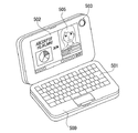
次に、図41に示したのは、撮像ユニット900をパソコン500に用いた例である。図41は、パソコン500の概略構成を説明するための斜視説明図である。
パソコン500は、キーボード501、モニター部502および撮像部503を備えている。モニター部502は、撮像部503で撮られた画像も含む画像505を表示することができる構成とされている。撮像部503は、モニター部502の横に設けられている。撮像ユニット900(不図示)は、撮像部503の内部に設けられており、光軸方向断面が、図40(c)に示したのと同じ構成を備えている。
【0147】
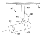
次に、図42に示したのは、撮像ユニット900を監視カメラ600に用いた例である。図42は、監視カメラ600の概略構成を説明するための側面視説明図である。
監視カメラ600は、監視カメラ本体をなす回路部605と撮像部607とを備え、天井608に固定された取付部601に、軸602およびモータ603を介して取り付けられている。撮像部607の内部には、図示真直矢印方向が撮像可能となるように、撮像ユニット900が設けられている。撮像ユニット900は、光軸方向断面が、図40(c)に示したのと同じ構成を備え、撮像部607内に固定されている。基板取付部410(図40(c)参照)は、不図示の回動機構により首振り運動可能に取り付けてもよい。
【0148】
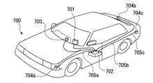
次に、図43に示したのは、撮像ユニット900を自動車の車載用カメラシステム700に用いた例である。図43は、車載用カメラシステム700の概略構成を説明するための斜視説明図である。
車載用カメラシステム700は、撮像部704a、b、cを備え、信号処理部702および切換制御部703を介してそれぞれの撮像部により撮影された画像をモニター部701に表示できるようにしたシステムである。撮像部704a、b、cは、それぞれ、光ファイバ705a、b、cによって結合されている。
撮像ユニット900は、光軸方向断面が、図40(c)に示したのと同じ構成を備え、撮像部704a、b、c内に固定されている。
【0149】
以上に説明した本実施形態に係る撮像装置によれば、いずれも本発明の第1の実施形態に係る撮像レンズユニットを用いているので、第1の実施形態の撮像レンズユニットと同様の作用効果を奏する。
特に、ズームレンズ200によれば、鏡枠を用いることなく第2群G2、第3群G3のレンズ群を一体化しているので、軽量化・小型化を図ることができる。また、撮像ユニット900によれば、構成部材を重ねて接合するという共通の製造方法によってCCD902に一体化した構成を製作することができるので、製造工程が一貫するために生産性がよいという利点がある。さらに、それぞれをアレイ状の配列のまま接合してから切り出す方法によれば、より生産性が向上し、大量生産と、小型化に適するという利点がある。
【0150】
【発明の効果】
以上に述べたように、本発明に係る撮像レンズユニットによれば、空気間隔を備えることによって光学系の性能を向上しながら、鏡枠部材や鏡枠構造を設けることなく光学素子を一体化することによって、小型で安価な撮像レンズユニットが提供できるという効果を奏する。
また、本発明に係る撮像装置によれば、本発明に係る撮像レンズユニットを用いるので、本発明に係る撮像レンズユニットと同様の効果を奏することができる。
【図面の簡単な説明】
【図1】本発明の第1の実施形態に係る撮像レンズユニットを説明するための概略斜視図およびそのA−A断面図である。
【図2】本発明の第1の実施形態に係る撮像レンズユニットを製造するための一例を説明するための概略斜視図である。
【図3】同じく第1変形例を説明するための斜視説明図、そのB−B断面図および本変形例の製造方法の一例を説明するための光軸方向断面の概念図である。
【図4】同じく第2変形例を説明するための光軸方向の断面図および本変形例の製造方法の一例を説明するための光軸方向断面の概念図である。
【図5】同じく第3変形例を説明するための光軸方向の断面図および本変形例の製造方法の一例を説明するための光軸方向断面の概念図である。
【図6】同じく第4変形例を説明するための光軸方向の断面図および本変形例の製造方法の一例を説明するための光軸方向断面の概念図である。
【図7】同じく第5変形例を説明するための光軸方向の断面図および本変形例の製造方法の一例を説明するための光軸方向断面の概念図である。
【図8】本発明に係る第1の実施形態の光学素子アレイの切断形状の例を示す説明図である。
【図9】本発明の第1の実施形態に係る撮像レンズユニットの、第1の数値実施例の光路図である
【図10】同じく第1の数値実施例の収差図である。
【図11】同じく第1の数値実施例の構成における空気間隔の形成手段を説明する光軸方向断面図である。
【図12】本発明の第1の実施形態に係る撮像レンズユニットの、第2の数値実施例の光路図である
【図13】同じく第2の数値実施例の収差図である。
【図14】本発明の第1の実施形態に係る撮像レンズユニットの、第3の数値実施例の光路図である。
【図15】同じく第3の数値実施例の収差図である。
【図16】本発明の第1の実施形態に係る撮像レンズユニットの、第4の数値実施例の光路図である。
【図17】同じく第4の数値実施例の収差図である。
【図18】本発明の第1の実施形態に係る撮像レンズユニットの、第5の数値実施例の光路図である。
【図19】同じく第5の数値実施例の収差図である。
【図20】本発明の第1の実施形態に係る撮像レンズユニットの、第6の数値実施例の光路図である。
【図21】同じく第6の数値実施例の収差図である。
【図22】本発明の第1の実施形態に係る撮像レンズユニットの、第7の数値実施例の光路図である。
【図23】同じく第7の数値実施例の収差図である。
【図24】本発明の第1の実施形態に係る撮像レンズユニットの、第8の数値実施例の光路図である。
【図25】同じく第8の数値実施例の収差図である。
【図26】本発明の第1の実施形態に係る撮像レンズユニットの、第9の数値実施例の光路図である。
【図27】同じく第9の数値実施例の収差図である。
【図28】本発明の第1の実施形態に係る撮像レンズユニットの、第10の数値実施例の光路図である。
【図29】同じく第10の数値実施例の収差図である。
【図30】本発明の第1の実施形態に係る撮像レンズユニットの、第11の数値実施例の光路図である。
【図31】同じく第11の数値実施例の収差図である。
【図32】本発明の第1の実施形態に係る撮像レンズユニットの、第12の数値実施例のW位置における光路図である。
【図33】同じく第12の数値実施例のS、T位置における光路図である。
【図34】同じく第12の数値実施例の収差図(W)である。
【図35】同じく第12の数値実施例の収差図(S)である。
【図36】同じく第12の数値実施例の収差図(T)である。
【図37】本発明の第2の実施形態に係る撮像装置の一例であるズームレンズの光学系の概略構成を示す説明図である。
【図38】本発明の第2の実施形態に係る撮像装置の他の例となる撮像装置の主要部分である撮像ユニットの概略構成を示す光軸方向断面図である。
【図39】同撮像ユニットを用いたカプセル内視鏡の概略構成を示す断面説明図である。
【図40】同撮像ユニットを用いた携帯用端末の概略構成を示す正面図、側面図および断面図である。
【図41】同撮像ユニットを用いたパソコンの概略構成を示す斜視説明図である。
【図42】同撮像ユニットを用いた監視カメラの概略構成を示す側面視説明図である。
【図43】同撮像ユニットを用いた自動車の車載用カメラシステムの概略構成を示す斜視説明図である。
【符号の説明】
1、2、4、11、12、13、21、22、24、25 レンズ(光学素子)1a、1b、2a、2b、4a、4b、11a、11b、12a、12b、13a、13b、21a、21b、22a、22b、24a、24b、25a、25b レンズ面(光学面)
1c、2c、3c、4c、11c、12c、13c、21c、22c、24c、25c、152c フランジ側面(側面)
1d、2d、3d、4d、11d、12d、13d、21d、22d、24d、25d フランジ部
1e、2e、3e、22e、24e、25e、51a、52a、151a 位置決め突起
2f、3f、4f 位置決め溝
3 光学フィルター(光学フィルター部材)
6 切断線
23 開口絞り(挟持部材)
31 開口絞りコート
32 フレア防止コート
40 光学面
41 フード部材
51、57、60、65、69、73、76、80、87、92、96、211第1レンズ(光学素子)
52、58、61、66、70、74、77、82、88、93、97、212第2レンズ(光学素子)
53、59、62、67、71、75、78、83、90、94、98、213第3レンズ(光学素子)
54、55 フィルター部材(光学フィルター部材)
56 スペーサ(挟持部材)
63、68、72、79、84、91、95、214 第4レンズ(光学素子)81 平行平面板
85、215 第5レンズ(光学素子)
100、110、120、130、140、145、150、151、152、201、202 撮像レンズユニット
101、102、103、104、111、112、113、121、122、124、125 アレイ(光学素子アレイ)
123 開口絞りシート(挟持部材)
141 フードアレイ部材
200 ズームレンズ(撮像装置)
300 カプセル内視鏡(撮像装置)
400 携帯用端末(撮像装置)
405、503、607、704a、704b、704c 撮像部
500 パソコン(撮像装置)
600 監視カメラ(撮像装置)
700 車載用カメラシステム(撮像装置)
900、900’、900” 撮像ユニット
901、910 撮像素子
902 CCD[0001]
TECHNICAL FIELD OF THE INVENTION
The present invention relates to an imaging lens unit and an imaging device.
[0002]
[Prior art]
2. Description of the Related Art Conventionally, an imaging lens unit using a plurality of lenses, such as a camera lens, is configured such that a lens is polished or molded, and then arranged and fixed to each other by placing the lens on a lens frame that is accurately processed with metal or the like. And it was. And the imaging lens unit integrated with such a lens frame was attached to an imaging device provided with an imaging element.
[0003]
[0004]
[Patent Document 1]
JP-A-2002-243912 (Pages 1-10, FIGS. 1, 2, 8, 10, 12)
[0005]
[Problems to be solved by the invention]
However, the conventional imaging lens unit and imaging apparatus as described above have a problem that it is difficult to reduce the cost because the cost of material and processing of the lens frame and the cost of assembling the lens to the lens frame are required in addition to the lens manufacturing cost. was there. In particular, imaging devices such as security cameras and endoscopes, for example, tend to require increasingly smaller imaging lens units. Therefore, there has been a problem that manufacturing and assembling an imaging lens unit used in such an imaging apparatus has become more and more troublesome, which has increased manufacturing time and manufacturing cost.
[0006]
Further, in the technology described in
[0007]
The present invention has been made in view of such a problem, and an object of the present invention is to provide an imaging lens unit and an imaging apparatus that can be manufactured in large quantities and at low cost even if they are small.
[0008]
[Means for Solving the Problems]
In order to solve the above problem, according to the first aspect of the invention, in the imaging lens unit, a plurality of optical elements that are overlapped with their optical axes aligned are joined to each other, and the side surface of each optical element is the optical element. They are arranged in the same plane extending linearly in the direction along the axis.
According to the present invention, the imaging lens unit can be configured without using a lens frame or the like for fixing the optical element by overlapping and joining the optical elements to each other. Further, an imaging lens unit that can be stably held and fixed by using the side surface of an optical element disposed in the same plane that extends linearly in the direction along the optical axis is provided. .
[0009]
In the invention according to
According to the present invention, since the optical axes of a plurality of optical elements are aligned at once, the alignment step can be greatly reduced. In addition, since the positioning and joining of the optical elements are performed in a state of a relatively large optical element array, handling can be facilitated and workability can be improved. Further, since the optical element array is cut off, the small-sized imaging lens unit can be manufactured in large quantities.
[0010]
According to a third aspect of the present invention, in the imaging lens unit according to the second aspect, a maximum outer diameter of the imaging lens unit in a cross section orthogonal to an optical axis of MD, and an ED configured by the plurality of optical elements. When the maximum beam effective diameter of the system is defined, a configuration satisfying the following relational expression is used.
1.0 <MD / ED <4.0
According to the present invention, since the MD / ED is provided with an upper limit and the size of the portion where the light beam does not enter is limited, the number of optical elements arranged on one optical element array can be increased. Then, when cutting the joined optical element array, it is possible to set a large number of products per man-hour for cutting, and it is possible to reduce material cost and production cost. In addition, when molding the optical element array, it is not necessary to use a large-sized mold, so that high-precision molding is possible.
[0011]
Here, the maximum outer diameter of the imaging lens unit in a cross section orthogonal to the optical axis means the diameter of the smallest cylinder among the virtual cylinders including the imaging lens unit with the optical axis as the central axis. For example, when the imaging lens unit is cut into a cylindrical shape, the diameter is the diameter of the cylinder, and when the imaging lens unit is cut into a regular polygonal prism, the diameter is the diameter of the circumscribed cylinder.
Further, the lower limit of MD / ED is a trivial necessary condition for the maximum effective beam diameter to fall within a predetermined outer diameter.
[0012]
Note that in order to further increase the number of imaging lens units per optical element array and improve productivity, it is desirable to set MD / ED to a smaller value. Therefore, the imaging lens unit
1.0 <MD / ED <3.0
Is preferably satisfied. Moreover,
1.0 <MD / ED <2.0
Is preferably satisfied.
[0013]
According to a fourth aspect of the present invention, in the imaging lens unit according to the second aspect, when the total of the cutting lengths in the direction along the optical axis is defined as a distance TT, a configuration satisfying the following relationship is used. .
TT <20mm
According to the present invention, by setting the cutting length smaller than the upper limit value, the cutting time of the optical element array can be shortened and can be set in a reasonable range, so that productivity can be improved. Further, since the generation of heat at the time of cutting is reduced, the thermal distortion of the optical element can be reduced even when cutting is performed continuously, so that productivity can be improved while maintaining high performance.
[0014]
In order to cut in a shorter time, TT is desirably set to a smaller value. Therefore, the imaging lens unit
TT <15mm
Is preferably satisfied. Moreover,
TT <10mm
Is preferably satisfied.
[0015]
According to a fifth aspect of the present invention, in the imaging lens unit according to any one of the first to fourth aspects, a configuration is used in which a side surface of each of the optical elements is substantially parallel to an optical axis.
According to the present invention, since the side surface can be easily formed, the production can be performed easily and quickly.
[0016]
According to a sixth aspect of the present invention, in the imaging lens unit according to any one of the second to fifth aspects, a configuration is used in which the optical element array is a two-dimensional array of optical elements.
According to the present invention, the optical axes of more optical elements can be easily adjusted. In addition, since the side surfaces of many optical elements can be formed by one cutting, the cutting efficiency can be improved. As a result, productivity can be improved, which is suitable for mass production.
[0017]
According to a seventh aspect of the present invention, in the imaging lens unit according to any one of the first to sixth aspects, at least one positive lens and at least one negative lens disposed adjacent to the positive lens are provided. And a configuration including an optical element having 10 or less power.
According to the present invention, aberration correction can be performed by combining the powers of the adjacent positive lens and negative lens.
Further, by setting the number of superposed optical elements to 10 or less, it is possible to maintain good optical performance without excessively accumulating misalignment errors. In order to further improve the optical performance, it is desirable to reduce the number of optical elements having power, and desirably eight or less. More preferably, the number is set to seven or less.
Here, the positive lens and the negative lens mean a lens having a positive power and a lens having a negative power, respectively.
[0018]
According to an eighth aspect of the present invention, in the imaging lens unit according to any one of the first to seventh aspects, a configuration having an air interface of 10 or less is used.
According to the present invention, it is possible to reduce the occurrence of ghost and flare due to light reflected at the air interface. As a result, good image quality can be obtained even if the degree and the number of antireflection coatings applied to the optical element are reduced, so that the manufacturing cost can be reduced without lowering the image quality.
It is to be noted that such an effect becomes more conspicuous as the number of air interfaces is smaller. Therefore, the number of air interfaces is preferably eight or less. Further, it is more preferable to set the number of air interfaces to 6 or less.
[0019]
According to a ninth aspect of the present invention, in the imaging lens unit according to any one of the first to eighth aspects, a configuration is used in which a process of providing a light absorbing member on a surface excluding an optical surface of the optical element is performed.
According to the present invention, since the reflected light on the surface of the optical element other than the optical surface is absorbed, the occurrence of ghost and flare can be suppressed. As a result, image quality can be improved.
[0020]
According to a tenth aspect of the present invention, in the imaging lens unit according to any one of the first to ninth aspects, the optical element includes an optical filter member having a side surface disposed in the same plane as a side surface of the optical element. Use the joined configuration.
According to the present invention, since the optical filter member can be integrated with the imaging lens unit, the function of the imaging lens unit can be improved and the size can be reduced. Further, since the optical filter member can be joined by the same operation as the other optical elements, the process is simplified and the productivity is improved.
[0021]
According to an eleventh aspect of the present invention, in the imaging lens unit according to any one of the first to tenth aspects, a hood member having a side surface disposed in the same plane as a side surface of the optical element is joined to the optical element. The configuration used is used.
According to the present invention, the hood member can suppress the occurrence of ghosts and flares caused by external light, so that image quality can be improved. Further, since the hood member can be joined by the same operation as the other optical elements, the process is simplified, and the productivity is improved.
[0022]
According to a twelfth aspect of the present invention, an imaging device includes the imaging lens unit according to any one of the first to eleventh aspects.
According to the present invention, it is possible to provide an imaging apparatus having the same operation and effect as the invention according to any one of the first to eleventh aspects.
[0023]
According to a thirteenth aspect of the present invention, in the imaging device according to the twelfth aspect, a configuration is used in which an imaging element is joined to an optical element constituting a final surface of the imaging lens unit.
According to the present invention, the imaging lens unit can be joined to the imaging device without having a complicated mounting structure. As a result, manufacturing costs can be reduced.
Further, the positioning accuracy between the optical element and the imaging element is improved.
[0024]
According to a fourteenth aspect of the present invention, in the imaging device according to the thirteenth aspect, a configuration is used in which the imaging element has an end surface disposed in the same plane as a side surface of the optical element.
According to the present invention, such an imaging device is obtained as follows. That is, a plurality of image sensors are arranged on one wafer. On the other hand, a plurality of the same optical elements are arranged on one substrate (optical element array). This optical element array is joined in a state where the optical axes of the optical elements are aligned and overlapped. Then, it is further aligned with and bonded to the wafer. Then, the image pickup unit can be manufactured by cutting them along a plane extending linearly in the direction along the optical axis. With this configuration, the positioning of the plurality of imaging elements and the plurality of optical elements can be performed at the same time, so that the positioning process is significantly simplified, and the productivity can be improved. Further, the manufacturing cost can be reduced.
[0025]
BEST MODE FOR CARRYING OUT THE INVENTION
Hereinafter, an imaging lens unit and an imaging device according to an embodiment of the present invention will be described with reference to the accompanying drawings.
[First Embodiment]
First, an imaging lens unit according to a first embodiment of the present invention will be described. FIG. 1A is a schematic perspective view illustrating an
[0026]
The
[0027]
The
[0028]
The
[0029]
The
[0030]
Further, on the
Further, a tip end surface in the optical axis direction of the
[0031]
Similarly, positioning
[0032]
In FIG. 1, an example of the shape of the positioning portion is exaggerated for the sake of clarity. However, any size and shape can be used as long as the position can be regulated in the optical axis direction and the direction orthogonal to the optical axis. It doesn't matter. For example, in the form of fitting with each other, in addition to the positioning protrusion 1e and the
[0033]
Appropriate means can be adopted as a means for joining the
[0034]
Each optical element can be manufactured by molding glass or synthetic resin. In particular, for an optical element having power, it is preferable to use glass as a material in order to realize more stable optical characteristics and achieve further miniaturization. This is because glass has a large refractive index, excellent surface accuracy, and excellent glass material uniformity and temperature stability.
[0035]
The
[0036]
The positioning of the
[0037]
In the
[0038]
Next, the operation of the
[0039]
Further, according to the present embodiment, since the positioning portion in the optical axis direction is integrally provided on the
[0040]
Further, in the present embodiment, since the
A projection is formed on the outer periphery of the
[0041]
As described above, the
[0042]
In the above description, an example in which the number of optical elements having power is three has been described. However, it is needless to say that the number of optical elements may be increased to improve the optical performance. At this time, by providing at least one positive lens and at least one negative lens, aberration correction can be performed.
Further, it is preferable that the number of superposed optical elements having power is 10 or less. With such a configuration, it is possible to prevent the misalignment error from being excessively accumulated due to a processing error of the positioning portion, an assembly error of the optical element, and the like. Further, the number of stacked optical elements having power is more preferably 8 or less, and further preferably 7 or less. The number of stacked optical elements can be determined comprehensively from the relationship between the performance required for the
[0043]
In the above description, the size of the air gap is not particularly limited, but it is preferable to set a limit on the size of the air gap. If the air gap is kept at an appropriate size, the length of the positioning portion in the optical axis direction becomes short, and processing with high dimensional accuracy becomes easy. As a result, misalignment errors can be prevented during assembly.
Specifically, TD is defined as a surface interval on the optical axis (the entire length of the optical system) from the first surface to the final surface of the optical system formed by joining the optical elements, and ST is defined as an air interval on the optical axis. When the sum of lengths (sum of air intervals) and MT are defined as the maximum value of the length of air intervals on the optical axis (maximum air interval), it is preferable that the imaging lens unit simultaneously satisfies the following formula.
ST / TD <0.7 (1)
MT / TD <0.5 (2)
If the upper limit of each of the above equations is exceeded, the air gap or the total length of the optical system becomes longer, so that the misalignment becomes larger. As a result, it becomes difficult to obtain sufficient optical performance.
Further, in order to further improve the assembling / processing accuracy of the optical element, it is preferable to satisfy the following expressions (3) and (4) instead of the expressions (1) and (2).
ST / TD <0.6 (3)
MT / TD <0.4 (4)
In order to further improve the assembling / processing accuracy of the optical element, it is preferable that the following expressions (5) and (6) are satisfied instead of the expressions (1) and (2).
ST / TD <0.5 (5)
MT / TD <0.3 (6)
[0044]
Further, in the above description, the number of the air interfaces of the optical element is eight, but the number of the air interfaces may be limited. Then, stray light which is likely to be generated at the air interface can be reduced. As a result, ghost and flare can be prevented from occurring, and the image quality can be improved. Further, the optical surface that needs to be subjected to the anti-reflection coating treatment can be eliminated or reduced, and the cost can be reduced.
Therefore, it is preferable to limit the number of air interfaces to less than ten. In order to further reduce the stray light, the number of air interfaces is more preferably less than 8, more preferably less than 6.
[0045]
Further, in the above description, an example in which the shape of the optical surface is not particularly limited has been described. However, it is preferable that the curved shape of the optical element is limited so that the inclination is gentle. This enables measurement with a contact-type shape measuring device such as Form Tali Surf. By using the contact type shape measuring device, the shape error can be directly known. Therefore, the quality of the component can be determined without measuring the optical characteristics. Also, by feeding back the measurement results to the manufacturing process, the manufacturing process can be improved. Further, the shape of the optical surface can be measured quickly. As a result, there is an advantage that the efficiency of manufacturing the optical surface having power according to the present embodiment can be improved.
Specifically, when the inclination angle θ is defined as the angle between the optical axis on the optical surface of the optical element and the normal to the optical surface, the inclination angle θ of each optical surface of the optical element is set to a maximum value of 60. It is preferable to make it smaller than the degree. If the maximum value of the inclination angle θ is smaller than 55 degrees, the measurement accuracy can be further increased even when the shape error is large, so that it is easy to manufacture an accurate optical surface, which is preferable. Further, it is more preferable that the maximum value of the inclination angle θ be smaller than 50 degrees.
[0046]
Next, some modified examples of the present embodiment will be described. In each case, the points different from the embodiment described above will be mainly described. In the description of the modified example, the same reference numerals are given to members common to the description of the above-described first embodiment, and the description is omitted.
First, a first modified example will be described. FIG. 3A is a perspective explanatory view for explaining a first modified example of the present embodiment. FIG. 3B is a cross-sectional view taken along a line BB of FIG. 3C and 3D are conceptual diagrams of a cross section in the optical axis direction for explaining an example of the manufacturing method of the first modified example.
[0047]
As shown in FIGS. 3A and 3B, the
[0048]
The
[0049]
The
The
0 <| φ / φ A | <0.5 (7)
To satisfy. Here, | a | indicates the absolute value of a.
[0050]
In this modification, unlike the case of the
[0051]
According to this modification, three optical elements are provided, and one of them is a cemented lens having optical surfaces cemented. Therefore, chromatic aberration can be corrected by appropriately selecting the refractive indexes of the bonded optical elements. As a result, a high-performance imaging lens unit with little chromatic aberration can be obtained.
[0052]
In addition, since the power φ at the joint surface is configured to satisfy Expression (7), the radius of curvature of the joint surface does not have to be excessively small, so that the machining of the joint surface is facilitated. As a result, the optical surface used as the bonding surface can be manufactured at low cost.
In this modification, the number of cemented lenses is one, but the number of cemented surfaces may be increased in order to further improve chromatic aberration. In this case, φ in Expression (7) is to be read as the maximum value of the power of the joint surfaces.
[0053]
In order to further improve the workability of the joint surface, it is preferable to satisfy the following expression instead of the expression (7) so as to increase the radius of curvature.
0 <| φ / φ A | <0.4 (8)
In order to further improve the workability of the joint surface, it is preferable to satisfy the following expression instead of the expression (7).
0 <| φ / φ A | <0.3 (9)
[0054]
Next, a second modified example will be described. FIG. 4A is a cross-sectional view in the optical axis direction for explaining a second modification of the present embodiment. 4B and 4C are conceptual diagrams of a cross section in the optical axis direction for explaining an example of the manufacturing method of the second modification.
As shown in FIG. 4A, the
[0055]
The
[0056]
The
The
The
[0057]
As shown in FIGS. 4B and 4C, such an
[0058]
According to the present modification, a predetermined air gap can be formed between the
Further, according to the present modification, the
[0059]
Next, a third modified example will be described. FIG. 5A is a cross-sectional view in the optical axis direction for describing a third modification of the present embodiment. FIGS. 5B and 5C are conceptual diagrams of a cross section in the optical axis direction for describing an example of a manufacturing method according to a third modification.
As shown in FIG. 5A, an
[0060]
However, an
[0061]
Both the
[0062]
According to this modification, since the
[0063]
Next, a fourth modification will be described. FIG. 6A is a cross-sectional view in the optical axis direction for describing a fourth modification of the present embodiment. 6B and 6C are conceptual diagrams of a cross section in the optical axis direction for explaining an example of a manufacturing method according to a fourth modification.
As shown in FIG. 6A, the
[0064]
In this modification, a
The
Also in the present modification, a manufacturing method in which the
[0065]
According to the present modification, since the
[0066]
Next, a fifth modification will be described. FIG. 7A is a cross-sectional view in the optical axis direction for describing a fifth modification of the present embodiment. 7B and 7C are conceptual diagrams of a cross section in the optical axis direction for describing an example of a manufacturing method according to a fifth modification.
As shown in FIG. 7A, the
[0067]
The
The
[0068]
Such an
TT <20mm (10)
[0069]
The maximum outer diameter of the
1.0 <MD / ED <4.0 (11)
In this modification, the
[0070]
According to this modification, since the distance TT satisfies the expression (10), the
Further, in order to improve productivity by cutting in a shorter time, it is desirable to set the distance TT to a smaller value. Therefore,
TT <15mm (12)
Is preferably satisfied. Moreover,
TT <10mm (13)
Is preferably satisfied.
[0071]
Further, according to the present modification, since the MD / ED satisfies the expression (11), the size of the portion through which the light flux does not pass is set to a reasonable range, and a reasonable number of optical elements for manufacturing is used. It can be arranged on an optical array element. As a result, there is an advantage that the number of imaging lens units manufactured per cutting man-hour can be increased and productivity can be improved.
Further, in order to further increase the number of imaging lens units per optical element array and further improve productivity, it is desirable to set MD / ED to a smaller value. Therefore,
1.0 <MD / ED <3.0 (14)
Is preferably satisfied. Moreover,
1.0 <MD / ED <2.0 (15)
Is preferably satisfied.
[0072]
In the above description of the fifth modification, an example has been described in which the thickness of the
Further, in the present modification, the distance TT is equal to the thickness of the joining portion, but the distance TT may be any length as long as it is the total length that is actually cut. For example, in the example shown in FIG. 1, the cut portion is different from the joint portion, and the cut portion is shorter than the joint portion. Further, in the example shown in FIG. 2, a
[0073]
In the first embodiment described above, an example has been described in which the side surfaces of the optical element are aligned with a quadrangular prism surface having a substantially square cross section. However, the present invention is not limited to such a prism surface. Various other shapes can be adopted depending on the manufacturing reason of the imaging lens unit and the convenience of handling such as assembly and conveyance.
[0074]
For example, linear processing is easy in manufacturing. Therefore, the number of steps is reduced particularly when cutting is performed from the optical element array, and the use of this processing method improves the production efficiency. In processing, the outer shape of the imaging lens unit does not need to be a square cross section, and may be, for example, a quadrangular prism surface having a rhombic cross section as shown in FIG. In this case, unlike the case of the square cross section, when the
[0075]
In particular, if a cutting method using a laser, a water jet, or the like is used, a plane / curved surface extending linearly in the direction along the optical axis can be easily formed, so that a circular cross section as shown in FIG. May be cut out. Such an imaging lens unit aligned on a cylindrical surface is extremely easy to mount because there is no direction around the optical axis when the alignment surface is used as a receiving reference surface for mounting.
[0076]
Further, in the above description, the side surface of the optical element has been described as being substantially parallel to the optical axis, but may be inclined with respect to the optical axis. For example, a tilt may occur due to a processing error at the time of cutting, or a tilt may be provided to align with a predetermined weight surface.
[0077]
In the above description, each optical element has a
[0078]
In the above description, an example in which the side surfaces of the optical element are aligned has been described as an example that is convenient for manufacturing. However, the side surfaces of the optical elements do not have to be aligned in order to achieve the purpose of simply configuring the imaging lens unit in which the lens frame member is omitted. This is because the respective optical elements can be joined at the surfaces in the optical axis direction of the
[0079]
Further, in the above description, an example in which the optical element array is a two-dimensional array is illustrated and described, but it is needless to say that a one-dimensional array may be used.
In the case of manufacturing by cutting out from an optical element array, a plurality of optical elements may be cut out in the arrangement direction to form an imaging lens unit having a plurality of parallel optical axes. At this time, the plurality of optical elements in the arrangement direction may have different types of optical surfaces.
[0080]
Specific numerical examples of the optical system that can be used in the imaging lens unit according to the first embodiment described above will be described below.
In the following, common to each embodiment, the symbol ω indicates a diagonal full angle of view, F indicates an effective F number, So indicates an object point distance, and IH indicates an image height. ST / TD, MT / TD, inclination angle θ, | φ / φ A The quantities |, TT, MD / ED have the same names and definitions as used in the above description.
In the numerical data table described later, r is the radius of curvature, d is the surface interval, n d Is the refractive index, ν d Represents Abbe number. r i , D i , N i, ν i (I is an integer) is a radius of curvature, a surface interval, a refractive index, and an Abbe number. In each optical path diagram described later, r in the table of numerical data is shown. i , D i , N i Is shown.
[0081]
[Example 1]
FIG. 9 is an optical path diagram of the first numerical example. FIG. 10 is an aberration diagram of the present embodiment. FIG. 10A shows the spherical aberration calculated for wavelengths of 656.27 nm, 587.56 nm, 546.07 nm, 486.13 nm, and 435.84 nm. FIG. 3 is an aberration diagram showing an aperture ratio. FIG. 10B is an aberration diagram in which the horizontal axis represents astigmatism (unit: mm) and the vertical axis represents angle of view (unit: °). ΔM represents a shift amount of the meridional image plane, and ΔS represents a shift amount of the sagittal image plane. FIG. 10C is an aberration diagram in which the horizontal axis represents distortion (unit%) and the vertical axis represents angle of view (unit °).
[0082]
The configuration of the present embodiment includes, in order from the object side, a
As shown in FIG. 11 (a), the air gap between the
In addition, all the air gaps of other numerical examples described below can be formed by any of the above means.
[0083]
In the present embodiment, the hyperfocal distance is set with the object point distance So = 960 mm. The total diagonal angle of view is ω = 40 °, the effective F number is F2.8, and the image height is IH = 0.924 mm.
In addition, there are 6 air interfaces, ST / TD = 0.42, MT / TD = 0.20, inclination angle θ is 33 °, | φ / φ A | = 0.08.
By providing an air gap between the
[0084]
As can be seen from FIG. 10, the imaging lens unit of the present example has good aberration characteristics in the visible light range.
[0086]
[Example 2]
FIG. 12 is an optical path diagram of the second numerical example. FIG. 13 is an aberration diagram of the present embodiment. FIGS. 13A, 13B, and 13C are drawn in the same manner as the graphs described in FIGS. 10A, 10B, and 10C, respectively, and the description of the graph axes and the like is omitted. I do.
[0087]
The configuration of this embodiment includes, in order from the object side, a
[0088]
In the present embodiment, the hyperfocal distance is set with the object point distance So = 960 mm. The total diagonal angle of view is ω = 40 °, the effective F number is F2.8, and the image height is IH = 0.924 mm.
In addition, 6 air interfaces, ST / TD = 0.14, MT / TD = 0.09, inclination angle θ is 37 °, | φ / φ A | = 0.09.
By providing an air gap between the
[0089]
As can be seen from FIG. 13, the imaging lens unit of the present example has good aberration characteristics in the visible light range.
[0091]
[Example 3]
FIG. 14 is an optical path diagram of the third numerical example. FIG. 15 is an aberration diagram of the present embodiment. FIGS. 15A, 15B, and 15C are drawn in the same manner as the graphs described in FIGS. 10A, 10B, and 10C, respectively, and the description of the graph axes and the like is omitted. I do.
[0092]
The configuration of the present embodiment includes, in order from the object side, a first lens 60 having negative power, a
[0093]
In this embodiment, the object point distance is So = 10 mm, the total diagonal angle of view is ω = 90 °, the effective F number is F3.0, and the image height is IH = 0.924 mm.
In addition, there are 6 air interfaces, ST / TD = 0.07, MT / TD = 0.04, the inclination angle θ is 46 °, | φ / φ A | = 0.07.
By providing an air gap between the
[0094]
As can be seen from FIG. 15, the imaging lens unit of this example has good aberration characteristics in the visible light range. In particular, it can be seen from FIG. 15A that the chromatic aberration is favorably corrected compared to the first and second embodiments because two sets of cemented lenses are used. Further, as shown in FIG. 15B, astigmatism is also corrected very well.
[0096]
[Example 4]
FIG. 16 is an optical path diagram of the fourth numerical example. FIG. 17 is an aberration diagram of the present embodiment. FIGS. 17 (a), (b), and (c) are drawn in the same manner as the graphs described in FIGS. 10 (a), (b), and (c), respectively, and the description of the graph axes and the like is omitted. I do.
[0097]
The configuration of this embodiment includes, in order from the object side, a
[0098]
In this embodiment, the object point distance is So = 10 mm, the total diagonal angle of view is ω = 90 °, the effective F number is F3.0, and the image height is IH = 0.924 mm.
In addition, there are four air interfaces, ST / TD = 0.09, MT / TD = 0.04, the inclination angle θ is 45 °, | φ / φ A | = 0.04.
By providing an air gap between the
[0099]
As can be seen from FIG. 17, the imaging lens unit of this example has good aberration characteristics in the visible light range. In particular, it can be seen from FIG. 17A that the chromatic aberration is favorably corrected compared to the first and second embodiments because two sets of cemented lenses are used. Further, as shown in FIG. 17B, astigmatism is also corrected very well.
[0101]
[Example 5]
FIG. 18 is an optical path diagram of the fifth numerical example. FIG. 19 is an aberration diagram of the present embodiment. FIGS. 19 (a), (b), and (c) are drawn in the same manner as the graphs described in FIGS. 10 (a), (b), and (c), respectively, and the description of the graph axes and the like is omitted. I do.
[0102]
The configuration of this embodiment includes, in order from the object side, a
[0103]
In this embodiment, the object point distance is So = 10 mm, the total diagonal angle of view is ω = 90 °, the effective F number is F3.0, and the image height is IH = 0.924 mm.
In addition, there are 6 air interfaces, ST / TD = 0.07, MT / TD = 0.03, inclination angle θ is 41 °, | φ / φ A | = 0.06.
By providing an air gap between the
[0104]
As can be seen from FIG. 19, the imaging lens unit of the present example has good aberration characteristics in the visible light range. In particular, when looking at FIG. 19A, it can be seen that the chromatic aberration is favorably corrected compared to the first and second embodiments because two sets of cemented lenses are used. Further, as shown in FIG. 19B, astigmatism is also corrected very well.
[0106]
[Example 6]
FIG. 20 is an optical path diagram of the sixth numerical example. FIG. 21 is an aberration diagram of the present embodiment. FIGS. 21 (a), (b), and (c) are drawn in the same manner as the graphs described in FIGS. 10 (a), (b), and (c), respectively, and the description of the graph axes and the like is omitted. I do.
[0107]
The configuration of this embodiment includes, in order from the object side, a
[0108]
In the present embodiment, a polycarbonate resin is used for the
In the present embodiment, the hyperfocal distance is set with the object point distance So = 960 mm. The total diagonal angle of view is ω = 40 °, the effective F number is F2.8, and the image height is IH = 0.924 mm.
In addition, there are 6 air interfaces, ST / TD = 0.14, MT / TD = 0.09, inclination angle θ is 38 °, | φ / φ A | = 0.20.
By providing an air gap between the
[0109]
As can be seen from FIG. 21, the imaging lens unit of this example has good aberration characteristics in the visible light range despite using a synthetic resin lens made of polycarbonate having a relatively small refractive index. ing. As described above, in the present embodiment, since an inexpensive lens can be manufactured using a lens made of polycarbonate, which is a synthetic resin, there is an advantage that a low-cost imaging lens unit can be provided. The use of synthetic resin molding also has the advantage that positioning projections for providing an air gap can be easily provided.
[0111]
[Example 7]
FIG. 22 is an optical path diagram of the seventh numerical example. FIG. 23 is an aberration diagram of the present embodiment. FIGS. 23 (a), (b) and (c) are drawn in the same manner as the graphs described in FIGS. 10 (a), (b) and (c), respectively, and the description of the graph axes and the like is omitted. I do.
[0112]
The configuration of this embodiment includes, in order from the object side, a
[0113]
In the present embodiment, ZEONEX (registered trademark), which is a synthetic resin, is used for the
In this embodiment, the object point distance is So = 10 mm, the total diagonal angle of view is ω = 90 °, the effective F number is F3.0, and the image height is IH = 0.924 mm.
In addition, there are 6 air interfaces, ST / TD = 0.07, MT / TD = 0.03, the inclination angle θ is 46 °, | φ / φ A | = 0.20.
By providing an air gap between the
[0114]
As can be seen from FIG. 23, the imaging lens unit of the present example has good aberration characteristics in the visible light range despite being configured using two synthetic resin lenses having a relatively small refractive index. It has become something. In particular, it can be seen from FIG. 23A that the chromatic aberration is favorably corrected compared to the first and second embodiments because two sets of cemented lenses are used.
According to the present embodiment, since an inexpensive synthetic resin lens is used for two of the four lenses, there is an advantage that an inexpensive imaging lens unit can be configured.
[0116]
Example 8
FIG. 24 is an optical path diagram of the eighth numerical example. FIG. 25 is an aberration diagram of the present embodiment. FIGS. 25 (a), (b), and (c) are drawn in the same manner as the graphs described in FIGS. 10 (a), (b), and (c), respectively, and the description of the graph axes and the like is omitted. I do. However, FIG. 25A shows the results for only the wavelengths of 656.27 nm, 587.56 nm, and 486.13 nm because the data variation for each wavelength is small.
[0117]
The configuration of the present embodiment includes, in order from the object side, a first lens 80 having negative power, a
In this embodiment, the object point distance is So = ∞, the total diagonal angle of view is ω = 103 °, the effective F number is F4.3, and the image height is IH = 0.5 mm.
In addition, there are four air interfaces, ST / TD = 0.04, MT / TD = 0.03, the inclination angle θ is 45 °, | φ / φ A | = 0.23.
By providing an air gap between the first lens 80 and the plane-
[0118]
As can be seen from FIG. 25, the imaging lens unit of this example has good aberration characteristics in the visible light range.
The present embodiment is an example in which an air lens is formed by providing an air gap between a first lens 80 having power and a parallel
[0120]
[Example 9]
FIG. 26 is an optical path diagram of the ninth numerical example. FIG. 27 is an aberration diagram of the present embodiment. FIGS. 27 (a), (b), and (c) are drawn in the same manner as the graphs described in FIGS. 10 (a), (b), and (c), respectively, and description of the graph axes and the like is omitted. I do. Further, H, D shown in FIG. 1 , D 2 Is the same amount as described in FIG.
[0121]
The configuration of the present embodiment includes, in order from the object side, a
The
The
The
In the present embodiment, the object point distance is set to So = 260 mm and the hyperfocal distance is set. The focal length is f = 1.47 mm, the total diagonal angle of view is ω = 66 °, the effective F-number is F2.8, and the image height is IH = 0.924 mm. Further, H = TT = 5.14 mm, D 1 = 4.62 mm, D 2 = 2.62. Therefore, MD / ED = D 1 / D 2 = 1.76.
[0122]
The aspheric surface is a rotationally symmetric aspheric surface given by the following definition expression.
Z = (y 2 / R) / [1+ {1- (1 + k) y 2 / R 2 } 1/2 ] + Ay 4 + By 6 + Cy 8 + Dy 10 + ... (16)
Here, Z is an optical axis (on-axis principal ray) where the traveling direction of light is positive, and y is a direction perpendicular to the optical axis. here,
R is a paraxial radius of curvature, k is a conical constant, and a, b, c, d,... Are fourth-, sixth-, eighth-, and tenth-order aspherical coefficients, respectively. The Z axis of this definition expression is the axis of the rotationally symmetric aspherical surface. Note that a term relating to an aspheric surface for which no data is described is zero.
[0123]
In this embodiment, TT and MD / ED satisfy Expressions (13) and (15), respectively. As a result, the imaging lens unit has excellent cutting workability.
[0125]
[Example 10]
FIG. 28 is an optical path diagram of the tenth numerical example. FIG. 29 is an aberration diagram of the present embodiment. FIGS. 29 (a), (b), and (c) are drawn in the same manner as the graphs described in FIGS. 10 (a), (b), and (c), respectively, and the description of the graph axes and the like is omitted. I do. Further, H, D shown in FIG. 1 , D 2 Is the same amount as described in FIG.
[0126]
The configuration of this embodiment includes, in order from the object side, a
The
The
The
In the present embodiment, the object point distance is set to So = 340 mm and the hyperfocal distance is set. The focal length is f = 1.67 mm, the total diagonal angle of view is ω = 60 °, the effective F-number is F2.8, and the image height is IH = 0.924 mm. Then, H = TT = 5.80 mm, D 1 = 5.42 mm, D 2 = 3.62. Therefore, MD / ED = 1.50. The following aspherical expression is the expression (16) described in the ninth embodiment.
[0127]
As can be seen from FIG. 29, the imaging lens unit of this example has good aberration characteristics in the visible light range.
In this embodiment, TT and MD / ED satisfy Expressions (13) and (15), respectively. As a result, the lens has excellent cutting workability.
[0129]
[Example 11]
FIG. 30 is an optical path diagram of the eleventh numerical example. FIG. 31 is an aberration diagram of the present embodiment. FIGS. 31 (a), (b), and (c) are drawn in the same manner as the graphs described in FIGS. 10 (a), (b), and (c), respectively, and the description of the graph axes and the like is omitted. I do. Further, H, D shown in FIG. 1 , D 2 Is the same amount as described in FIG.
[0130]
In this embodiment, the
The
The
The
In the present embodiment, the object point distance is set to So = 440 mm and the hyperfocal distance is set. The focal length is f = 1.88 mm, the total diagonal angle of view is ω = 50 °, the effective F number is F2.8, and the image height is IH = 0.924 mm. Then, H = TT = 4.67 mm, D 1 = 3.58 mm, D 2 = 2.18 mm. Therefore, MD / ED = 1.64. The following aspherical expression is the expression (16) described in the ninth embodiment.
[0131]
As can be seen from FIG. 31, the imaging lens unit of this example has good aberration characteristics in the visible light range.
In this embodiment, TT and MD / ED satisfy Expressions (13) and (15), respectively. As a result, the lens has excellent cutting workability.
[0133]
[Example 12]
FIG. 32 is an optical path diagram of a twelfth numerical example in which a zoom lens optical system is configured using the imaging lens unit according to the first embodiment of the present invention. FIG. 32 is an optical path diagram on the widest angle side (abbreviated as W). FIG. 33A is an optical path diagram of the intermediate angle of view (abbreviated as S), and FIG. 33B is an optical path diagram of the most telephoto side (abbreviated as T). 33, 34, and 35 are aberration diagrams for the W, S, and T lens arrangements of the present embodiment, respectively. FIGS. 33 to 35 show FIGS. 10A to 10A, respectively, except that the vertical axis of astigmatism (each drawing (b)) and distortion (each drawing (c)) are represented by image height (unit: mm). ), (B), and (c) are drawn in the same manner as the graphs described above, and the description of the graph axes and the like is omitted. In addition, H shown in the figure 1 , H 2 Is the same amount as H described in FIG. 2 Is the same amount as described in FIG. In this embodiment, each lens group is cut as a regular hexagonal prism. 1 Is equal to the diameter of the circumscribed cylinder of a regular hexagonal prism.
[0134]
The configuration of this embodiment includes, in order from the object side, a first lens group G1 having negative power, a second lens group G2 having positive power, a third lens group G3 having positive power, and a
The first lens group G1 includes a
The second lens group G2 is manufactured by cutting a
In the third lens group G3, a
[0135]
In the present embodiment, the object point distance is set to So = 900 mm and the hyperfocal distance is set. The focal length is f = 1.53 mm (W) to 2.19 mm (S) to 2.99 mm (T), and the total diagonal angle of view is ω = 31.2 ° (W) to 22.9 ° (S). 17.2 ° (T), the effective F number is F2.73 (W) to F3.28 (S) to F3.97 (T), and the image height is IH = 0.924 mm.
Then, H which is the TT of the second lens group G2 and the third lens group G3. 1 , H 2 Is H 1 = 2.17, H 2 = 1.30. Also, D 1 = 4.84 mm, D 2 = 4.00 mm. Therefore, MD / ED = 1.21. The following aspherical expression is the expression (16) described in the ninth embodiment.
Further, in the following configuration parameter table, for simplicity, the values of the surface distances at the time of zooming are collectively described in the form of W to ST.
[0136]
As can be seen from FIGS. 34 to 36, the zoom lens according to the present embodiment has good aberration characteristics in the visible light range.
In this embodiment, the TT and MD / ED of the imaging lens unit forming the second lens group and the third lens group satisfy Expressions (13) and (15), respectively. As a result, the imaging lens unit has excellent cutting workability.
[0138]
In the description of the imaging lens unit according to the ninth to eleventh numerical examples, it is assumed that the optical element, the aperture stop, and the like that need to be aligned with the optical axis are joined and cut. Needless to say, if necessary, the cutting may be performed with another holding member such as a spacer or an optical filter member joined. Even in such a case, the ninth to eleventh numerical examples are examples in which TT satisfies Expression (13).
[0139]
[Second embodiment]
Next, an imaging device according to a second embodiment of the present invention will be described. The imaging device according to the present embodiment includes the imaging lens unit according to the first embodiment. Hereinafter, a specific example will be described.
[0140]
FIG. 37 is an explanatory diagram illustrating a schematic configuration of an optical system of a
The
The movable second group G2 and third group G3 are configured by imaging
[0141]
Next, FIG. 38 is a sectional view in the optical axis direction showing a schematic configuration of an
As shown in FIG. 38A, the
In this example, the
The
The
The
[0142]
FIG. 38B shows an example of another
[0143]
FIG. 38C shows an example of still another
Such a configuration can be easily manufactured by using a method of cutting the
[0144]
Hereinafter, a specific example of the imaging apparatus according to the present embodiment using the
FIG. 39 shows an example in which the
The
[0145]
Next, FIG. 40 illustrates an example in which the
The
As shown in FIG. 40 (c), inside the
[0146]
Next, FIG. 41 shows an example in which the
The
[0147]
Next, FIG. 42 shows an example in which the
The
[0148]
Next, FIG. 43 shows an example in which the
The in-
The
[0149]
According to the imaging apparatus according to the present embodiment described above, since the imaging lens unit according to the first embodiment of the present invention is used, the same operation and effect as those of the imaging lens unit according to the first embodiment. To play.
In particular, according to the
[0150]
【The invention's effect】
As described above, according to the imaging lens unit of the present invention, the optical element is integrated without providing the lens frame member or the lens frame structure while improving the performance of the optical system by providing the air gap. This provides an effect that a small and inexpensive imaging lens unit can be provided.
Further, according to the imaging device of the present invention, since the imaging lens unit of the present invention is used, the same effects as those of the imaging lens unit of the present invention can be obtained.
[Brief description of the drawings]
FIG. 1 is a schematic perspective view for explaining an imaging lens unit according to a first embodiment of the present invention, and an AA cross-sectional view thereof.
FIG. 2 is a schematic perspective view for explaining an example for manufacturing the imaging lens unit according to the first embodiment of the present invention.
FIG. 3 is a perspective explanatory view for explaining a first modified example, a BB sectional view thereof, and a conceptual view of a section along the optical axis for describing an example of a manufacturing method of the present modified example.
FIGS. 4A and 4B are a cross-sectional view in the optical axis direction for explaining a second modified example and a conceptual diagram of a cross section in the optical axis direction for explaining an example of a manufacturing method of the modified example.
FIG. 5 is a cross-sectional view in the optical axis direction for explaining a third modification and a conceptual diagram of a cross section in the optical axis direction for explaining an example of a manufacturing method of the present modification.
FIGS. 6A and 6B are a sectional view in the optical axis direction for explaining a fourth modified example and a conceptual diagram of a sectional view in the optical axis direction for explaining an example of a manufacturing method of this modified example;
FIGS. 7A and 7B are a sectional view in the optical axis direction for explaining a fifth modified example and a conceptual diagram of a sectional view in the optical axis direction for explaining an example of a manufacturing method of the modified example;
FIG. 8 is an explanatory diagram illustrating an example of a cut shape of the optical element array according to the first embodiment of the present invention.
FIG. 9 is an optical path diagram of a first numerical example of the imaging lens unit according to the first embodiment of the present invention.
FIG. 10 is an aberrational diagram of the first numerical example.
FIG. 11 is a sectional view in the optical axis direction for explaining a means for forming an air gap in the configuration of the first numerical example.
FIG. 12 is an optical path diagram of a second numerical example of the imaging lens unit according to the first embodiment of the present invention.
FIG. 13 is an aberrational diagram of the second numerical example.
FIG. 14 is an optical path diagram of a third numerical example of the imaging lens unit according to the first embodiment of the present invention.
FIG. 15 is an aberrational diagram of the third numerical example.
FIG. 16 is an optical path diagram of a fourth numerical example of the imaging lens unit according to the first embodiment of the present invention.
FIG. 17 is an aberrational diagram of the fourth numerical example.
FIG. 18 is an optical path diagram of a fifth numerical example of the imaging lens unit according to the first embodiment of the present invention.
FIG. 19 is an aberration diagram of the fifth numerical example.
FIG. 20 is an optical path diagram of a sixth numerical example of the imaging lens unit according to the first embodiment of the present invention.
FIG. 21 is an aberrational diagram of the sixth numerical example.
FIG. 22 is an optical path diagram of a seventh numerical example of the imaging lens unit according to the first embodiment of the present invention.
FIG. 23 is an aberrational diagram of the seventh numerical example.
FIG. 24 is an optical path diagram of an eighth numerical example of the imaging lens unit according to the first embodiment of the present invention.
FIG. 25 is an aberrational diagram of the eighth numerical example.
FIG. 26 is an optical path diagram of a ninth numerical example of the imaging lens unit according to the first embodiment of the present invention.
FIG. 27 is an aberrational diagram of the ninth numerical example.
FIG. 28 is an optical path diagram of a tenth numerical example of the imaging lens unit according to the first embodiment of the present invention.
FIG. 29 is an aberrational diagram of the tenth numerical example.
FIG. 30 is an optical path diagram of an eleventh numerical example of the imaging lens unit according to the first embodiment of the present invention.
FIG. 31 is an aberrational diagram of the eleventh numerical example.
FIG. 32 is an optical path diagram at the W position of a twelfth numerical example of the imaging lens unit according to the first embodiment of the present invention.
FIG. 33 is an optical path diagram at S and T positions in the twelfth numerical example.
FIG. 34 is an aberration diagram (W) of the twelfth numerical example.
FIG. 35 is an aberration diagram (S) of the twelfth numerical example.
FIG. 36 is an aberration diagram (T) of the twelfth numerical example.
FIG. 37 is an explanatory diagram illustrating a schematic configuration of an optical system of a zoom lens that is an example of an imaging device according to a second embodiment of the present invention.
FIG. 38 is a sectional view in the optical axis direction showing a schematic configuration of an image pickup unit which is a main part of an image pickup apparatus as another example of the image pickup apparatus according to the second embodiment of the present invention.
FIG. 39 is an explanatory sectional view showing a schematic configuration of a capsule endoscope using the imaging unit.
FIG. 40 is a front view, a side view, and a cross-sectional view illustrating a schematic configuration of a portable terminal using the imaging unit.
FIG. 41 is an explanatory perspective view showing a schematic configuration of a personal computer using the imaging unit.
FIG. 42 is an explanatory side view showing a schematic configuration of a surveillance camera using the imaging unit.
FIG. 43 is a perspective explanatory view showing a schematic configuration of a vehicle-mounted camera system using the imaging unit.
[Explanation of symbols]
1, 2, 4, 11, 12, 13, 21, 22, 24, 25 Lenses (optical elements) 1a, 1b, 2a, 2b, 4a, 4b, 11a, 11b, 12a, 12b, 13a, 13b, 21a, 21b, 22a, 22b, 24a, 24b, 25a, 25b Lens surface (optical surface)
1c, 2c, 3c, 4c, 11c, 12c, 13c, 21c, 22c, 24c, 25c, 152c Flange side surface (side surface)
1d, 2d, 3d, 4d, 11d, 12d, 13d, 21d, 22d, 24d, 25d Flange
1e, 2e, 3e, 22e, 24e, 25e, 51a, 52a, 151a Positioning protrusion
2f, 3f, 4f Positioning groove
3 Optical filter (optical filter member)
6 Cutting line
23 Aperture stop (clamping member)
31 Aperture draw coat
32 Flare prevention coat
40 optical surface
41 Hood material
51, 57, 60, 65, 69, 73, 76, 80, 87, 92, 96, 211 First lens (optical element)
52, 58, 61, 66, 70, 74, 77, 82, 88, 93, 97, 212 Second lens (optical element)
53, 59, 62, 67, 71, 75, 78, 83, 90, 94, 98, 213 Third lens (optical element)
54, 55 Filter member (optical filter member)
56 Spacer (clamping member)
63, 68, 72, 79, 84, 91, 95, 214 Fourth lens (optical element) 81 Parallel plane plate
85, 215 Fifth lens (optical element)
100, 110, 120, 130, 140, 145, 150, 151, 152, 201, 202 Imaging lens unit
101, 102, 103, 104, 111, 112, 113, 121, 122, 124, 125 Array (optical element array)
123 Aperture stop sheet (clamping member)
141 Food Array Member
200 zoom lens (imaging device)
300 capsule endoscope (imaging device)
400 Portable terminal (imaging device)
405, 503, 607, 704a, 704b, 704c Imaging unit
500 PC (imaging device)
600 surveillance camera (imaging device)
700 In-vehicle camera system (imaging device)
900, 900 ', 900 "imaging unit
901, 910 Image sensor
902 CCD
Claims (14)
以下の関係式を満足することを特徴とする請求項2に記載の撮像レンズユニット。
1.0<MD/ED<4.0When MD is defined as the maximum outer diameter of the imaging lens unit in a cross section orthogonal to the optical axis, and ED is defined as the maximum effective ray diameter of the optical system including the plurality of optical elements,
The imaging lens unit according to claim 2, wherein the following relational expression is satisfied.
1.0 <MD / ED <4.0
以下の関係を満足することを特徴とする請求項2に記載の撮像レンズユニット。
TT<20mmWhen the total of the cutting lengths in the direction along the optical axis is defined as a distance TT,
The imaging lens unit according to claim 2, wherein the following relationship is satisfied.
TT <20mm
Priority Applications (3)
| Application Number | Priority Date | Filing Date | Title |
|---|---|---|---|
| JP2002345449A JP2004088713A (en) | 2002-06-27 | 2002-11-28 | Image pickup lens unit and image pickup device |
| US10/601,910 US6954311B2 (en) | 2002-06-27 | 2003-06-24 | Image pickup lens unit and image pickup device |
| US11/048,881 US20050128597A1 (en) | 2002-06-27 | 2005-02-03 | Image pickup lens unit and image pickup device |
Applications Claiming Priority (2)
| Application Number | Priority Date | Filing Date | Title |
|---|---|---|---|
| JP2002188300 | 2002-06-27 | ||
| JP2002345449A JP2004088713A (en) | 2002-06-27 | 2002-11-28 | Image pickup lens unit and image pickup device |
Publications (1)
| Publication Number | Publication Date |
|---|---|
| JP2004088713A true JP2004088713A (en) | 2004-03-18 |
Family
ID=31996071
Family Applications (1)
| Application Number | Title | Priority Date | Filing Date |
|---|---|---|---|
| JP2002345449A Pending JP2004088713A (en) | 2002-06-27 | 2002-11-28 | Image pickup lens unit and image pickup device |
Country Status (2)
| Country | Link |
|---|---|
| US (2) | US6954311B2 (en) |
| JP (1) | JP2004088713A (en) |
Cited By (73)
| Publication number | Priority date | Publication date | Assignee | Title |
|---|---|---|---|---|
| JP2005018024A (en) * | 2003-05-30 | 2005-01-20 | Konica Minolta Opto Inc | Lens unit, imaging unit equipped with lens unit, and portable terminal |
| JP2006017795A (en) * | 2004-06-30 | 2006-01-19 | Konica Minolta Opto Inc | Lens unit and manufacturing method thereof |
| JP2006106479A (en) * | 2004-10-07 | 2006-04-20 | Towa Corp | Translucent member, optical device, and optical device assembling method |
| JP2007097192A (en) * | 2005-09-29 | 2007-04-12 | Visera Technologies Co Ltd | Wafer level image module |
| JP2007304162A (en) * | 2006-05-09 | 2007-11-22 | Ricoh Co Ltd | Optical elements, method of fixing and connecting the same, optical scanner and image forming apparatus |
| JP2008046563A (en) * | 2006-08-21 | 2008-02-28 | Nikon Corp | Optical module and manufacturing method therefor |
| JP2008258813A (en) * | 2007-04-03 | 2008-10-23 | Alps Electric Co Ltd | Camera module |
| JP2009147092A (en) * | 2007-12-13 | 2009-07-02 | Sharp Corp | Electronic element wafer module, electronic element module, sensor wafer module, sensor module, lens array plate, method of manufacturing sensor module, and electronic information equipment |
| JP2009533885A (en) * | 2006-04-17 | 2009-09-17 | オムニビジョン シーディーエム オプティクス, インコーポレイテッド | Arrayed imaging system and related method |
| JP2009240634A (en) | 2008-03-31 | 2009-10-22 | Olympus Corp | Endoscope apparatus |
| JP2009251210A (en) * | 2008-04-04 | 2009-10-29 | Konica Minolta Opto Inc | Imaging lens, imaging apparatus, electronic apparatus, portable terminal, and method for manufacturing imaging lens |
| WO2009157310A1 (en) * | 2008-06-25 | 2009-12-30 | コニカミノルタオプト株式会社 | Imaging optical system |
| JP2010049112A (en) * | 2008-08-22 | 2010-03-04 | Sanyo Electric Co Ltd | Lens unit and image capturing device |
| JP2010091823A (en) * | 2008-10-08 | 2010-04-22 | Olympus Corp | Method for manufacturing optical unit, method for manufacturing imaging unit, optical unit, and imaging unit |
| JP2010517432A (en) * | 2007-01-26 | 2010-05-20 | フレックストロニクス エーピー エルエルシー | Wafer level camera module and manufacturing method thereof |
| JP2010186092A (en) * | 2009-02-13 | 2010-08-26 | Olympus Corp | Method of manufacturing lens module, lens module, camera module, and electronic device |
| WO2010095332A1 (en) * | 2009-02-18 | 2010-08-26 | コニカミノルタオプト株式会社 | Lens unit, aligning method, image pickup device and method for manufacturing image pickup device |
| CN101957494A (en) * | 2009-07-14 | 2011-01-26 | 夏普株式会社 | Imaging lens system and manufacture method thereof and photographing module and manufacture method thereof |
| WO2011010510A1 (en) * | 2009-07-24 | 2011-01-27 | Jsr株式会社 | Image-capturing lens |
| JP2011028213A (en) * | 2009-06-26 | 2011-02-10 | Konica Minolta Opto Inc | Image pickup lens, image pickup device and mobile terminal device |
| JP2011508900A (en) * | 2007-12-19 | 2011-03-17 | ヘプタゴン・オサケ・ユキチュア | Spacer element and method for manufacturing spacer element |
| JP2011059580A (en) * | 2009-09-14 | 2011-03-24 | Fujifilm Corp | Method of manufacturing wafer-level lens array, wafer-level lens array, lens module and imaging unit |
| JP2011075836A (en) * | 2009-09-30 | 2011-04-14 | Fujifilm Corp | Element array, element array stack, and method for manufacturing the element array stack |
| WO2011055655A1 (en) * | 2009-11-05 | 2011-05-12 | コニカミノルタオプト株式会社 | Image pickup device, optical unit, wafer lens laminated body, and method for manufacturing wafer lens laminated body |
| WO2011055623A1 (en) * | 2009-11-09 | 2011-05-12 | コニカミノルタオプト株式会社 | Image pickup lens, image pickup device, and method for manufacturing electronic apparatus |
| US7985357B2 (en) | 2005-07-12 | 2011-07-26 | Towa Corporation | Method of resin-sealing and molding an optical device |
| JP2011248319A (en) * | 2010-04-28 | 2011-12-08 | Sharp Corp | Imaging lens and imaging module |
| JP2012070431A (en) * | 2004-01-26 | 2012-04-05 | Digital Optics Corp | Thin camera with sub-pixel resolution |
| US8193558B2 (en) | 2004-04-26 | 2012-06-05 | Towa Corporation | Optical electronic component |
| JP2012128238A (en) * | 2010-12-16 | 2012-07-05 | Nitto Kogaku Kk | Lens unit and bar code scanner |
| JP2012189912A (en) * | 2011-03-11 | 2012-10-04 | Sharp Corp | Optical element, optical element module, electronic element module, and electronic information apparatus |
| JP2012533775A (en) * | 2009-12-21 | 2012-12-27 | フラウンホッファー−ゲゼルシャフト ツァ フェルダールング デァ アンゲヴァンテン フォアシュンク エー.ファオ | Optical laminate and method for producing the same |
| JP2013007969A (en) * | 2011-06-27 | 2013-01-10 | Sharp Corp | Imaging lens, lens array, imaging lens producing method, and imaging module |
| JP2013020267A (en) * | 2007-04-24 | 2013-01-31 | Digitaloptics Corp | Auto focus/zoom module using wafer level optics |
| WO2013018316A1 (en) * | 2011-07-29 | 2013-02-07 | 富士フイルム株式会社 | Imaging lens and imaging device |
| US8373936B2 (en) | 2010-04-12 | 2013-02-12 | Sharp Kabushiki Kaisha | Image sensing lens and image sensing module |
| US8422147B2 (en) | 2011-04-05 | 2013-04-16 | Sharp Kabushiki Kaisha | Image pickup lens and image pickup module |
| US8462448B2 (en) | 2009-08-07 | 2013-06-11 | Sharp Kabushiki Kaisha | Image sensing module, imaging lens and code reading method |
| JP2013120193A (en) * | 2011-12-06 | 2013-06-17 | Konica Minolta Advanced Layers Inc | Imaging lens |
| WO2013105376A1 (en) | 2012-01-13 | 2013-07-18 | オリンパスメディカルシステムズ株式会社 | Endoscope tip component and endoscope |
| TWI402979B (en) * | 2007-12-13 | 2013-07-21 | Sharp Kk | Electronic element wafer module, electronic element module, sensor wafer module, sensor module, lens array plate, manufacturing method for the sensor module, and electronic information device |
| JP2013153537A (en) * | 2006-07-17 | 2013-08-08 | Digitaloptics Corp East | Camera system |
| JP2013195523A (en) * | 2012-03-16 | 2013-09-30 | Olympus Corp | Zoom lens and imaging apparatus using the same |
| JP5374667B1 (en) * | 2011-11-22 | 2013-12-25 | オリンパスメディカルシステムズ株式会社 | Endoscope objective optical system |
| WO2014006971A1 (en) * | 2012-07-03 | 2014-01-09 | オリンパスメディカルシステムズ株式会社 | Objective optical system for endoscope |
| US8641936B2 (en) | 2009-12-21 | 2014-02-04 | Fraunhofer-Gesellschaft Zur Foerderung Der Angewandten Forschung E.V. | Method for manufacturing an optical structure |
| US8937681B2 (en) | 2007-07-19 | 2015-01-20 | Digitaloptics Corporation | Camera module back-focal length adjustment method and ultra compact components packaging |
| US8945458B2 (en) | 2009-12-21 | 2015-02-03 | Fraunhofer-Gesellschaft Zur Foerderung Der Angewandten Forschung E.V. | Method and apparatus for producing a structure, molding tool |
| US8953087B2 (en) | 2004-04-08 | 2015-02-10 | Flir Systems Trading Belgium Bvba | Camera system and associated methods |
| US8970924B2 (en) | 2012-03-29 | 2015-03-03 | Fuji Xerox Co., Ltd. | Image reading device and image forming apparatus |
| US9118825B2 (en) | 2008-02-22 | 2015-08-25 | Nan Chang O-Film Optoelectronics Technology Ltd. | Attachment of wafer level optics |
| US9134671B2 (en) | 2012-03-29 | 2015-09-15 | Fuji Xerox Co., Ltd. | Image reading device and image forming apparatus |
| JP2016018150A (en) * | 2014-07-10 | 2016-02-01 | オリンパス株式会社 | Image-capturing unit manufacturing method and image-capturing unit |
| US9291799B2 (en) | 2012-03-16 | 2016-03-22 | Olympus Corporation | Zoom lens, image pickup apparatus using the same, and information processing apparatus |
| WO2016117120A1 (en) * | 2015-01-23 | 2016-07-28 | オリンパス株式会社 | Image pickup device and endoscope |
| JP2016522447A (en) * | 2013-05-27 | 2016-07-28 | フラウンホーファー−ゲゼルシャフト・ツール・フェルデルング・デル・アンゲヴァンテン・フォルシュング・アインゲトラーゲネル・フェライン | Optical structure provided with bridging member and method for manufacturing the same |
| US9419032B2 (en) | 2009-08-14 | 2016-08-16 | Nanchang O-Film Optoelectronics Technology Ltd | Wafer level camera module with molded housing and method of manufacturing |
| US9523798B2 (en) | 2009-09-30 | 2016-12-20 | Fujifilm Corporation | Element array and element array laminate |
| JP2017047169A (en) * | 2016-03-25 | 2017-03-09 | パナソニック株式会社 | Endoscope |
| WO2017072861A1 (en) * | 2015-10-27 | 2017-05-04 | オリンパス株式会社 | Imaging device and endoscope |
| JP2017195960A (en) * | 2016-04-25 | 2017-11-02 | パナソニック株式会社 | Endoscope |
| JP2017195965A (en) * | 2016-04-25 | 2017-11-02 | パナソニック株式会社 | Endoscope |
| JP2017195963A (en) * | 2016-04-25 | 2017-11-02 | パナソニック株式会社 | Endoscope |
| JP2018021947A (en) * | 2016-08-01 | 2018-02-08 | 日本電気硝子株式会社 | Optical lens |
| US10009528B2 (en) | 2011-02-24 | 2018-06-26 | Nan Chang O-Film Optoelectronics Technology Ltd | Autofocus camera module packaging with circuitry-integrated actuator system |
| WO2019138463A1 (en) * | 2018-01-10 | 2019-07-18 | オリンパス株式会社 | Method for manufacturing optical unit, optical unit, and endoscope |
| WO2019171725A1 (en) * | 2018-03-07 | 2019-09-12 | オリンパス株式会社 | Endoscope tip and endoscope |
| WO2020031261A1 (en) * | 2018-08-07 | 2020-02-13 | オリンパス株式会社 | Wafer lens, layered lens array, and endoscope |
| JP2020112792A (en) * | 2019-01-08 | 2020-07-27 | エーエーシー テクノロジーズ ピーティーイー リミテッド | Electronic apparatus having lens system and imaging function |
| WO2020183600A1 (en) * | 2019-03-12 | 2020-09-17 | オリンパス株式会社 | Endoscopic imaging device and endoscope |
| US10996456B2 (en) | 2016-04-25 | 2021-05-04 | Panasonic I-Pro Sensing Solutions Co., Ltd. | Endoscope and camera module |
| WO2021176512A1 (en) * | 2020-03-02 | 2021-09-10 | オリンパス株式会社 | Endoscope, optical laiminate, and method for manufacturing optical laminate |
| WO2021193085A1 (en) * | 2020-03-25 | 2021-09-30 | ソニーグループ株式会社 | Lens optical system, light receiving device, and distance measuring system |
Families Citing this family (104)
| Publication number | Priority date | Publication date | Assignee | Title |
|---|---|---|---|---|
| JP2004029554A (en) * | 2002-06-27 | 2004-01-29 | Olympus Corp | Image pickup lens unit and image pickup device |
| US20050245789A1 (en) | 2003-04-01 | 2005-11-03 | Boston Scientific Scimed, Inc. | Fluid manifold for endoscope system |
| US7591783B2 (en) | 2003-04-01 | 2009-09-22 | Boston Scientific Scimed, Inc. | Articulation joint for video endoscope |
| US20040199052A1 (en) | 2003-04-01 | 2004-10-07 | Scimed Life Systems, Inc. | Endoscopic imaging system |
| US7578786B2 (en) | 2003-04-01 | 2009-08-25 | Boston Scientific Scimed, Inc. | Video endoscope |
| US8118732B2 (en) | 2003-04-01 | 2012-02-21 | Boston Scientific Scimed, Inc. | Force feedback control system for video endoscope |
| US7068448B2 (en) * | 2004-07-23 | 2006-06-27 | Axon Technologies Corp. | Optical lens and lens system |
| US8083671B2 (en) | 2004-09-30 | 2011-12-27 | Boston Scientific Scimed, Inc. | Fluid delivery system for use with an endoscope |
| EP1799095A2 (en) | 2004-09-30 | 2007-06-27 | Boston Scientific Scimed, Inc. | Adapter for use with digital imaging medical device |
| US7479106B2 (en) * | 2004-09-30 | 2009-01-20 | Boston Scientific Scimed, Inc. | Automated control of irrigation and aspiration in a single-use endoscope |
| US7377876B2 (en) * | 2004-10-29 | 2008-05-27 | Tai-Her Yang | Split serial-parallel hybrid dual-power drive system |
| JP2006333120A (en) * | 2005-05-26 | 2006-12-07 | Denso Corp | Image sensing module |
| US7955255B2 (en) | 2006-04-20 | 2011-06-07 | Boston Scientific Scimed, Inc. | Imaging assembly with transparent distal cap |
| US8202265B2 (en) | 2006-04-20 | 2012-06-19 | Boston Scientific Scimed, Inc. | Multiple lumen assembly for use in endoscopes or other medical devices |
| KR100867520B1 (en) * | 2007-04-23 | 2008-11-07 | 삼성전기주식회사 | Imaging-lens and method of manufacturing the same |
| TWI403775B (en) * | 2007-07-13 | 2013-08-01 | Asia Optical Co Inc | A lens group with a chimeric structure and a lens module |
| KR100956250B1 (en) * | 2007-12-10 | 2010-05-06 | 삼성전기주식회사 | Method for Manufacturing a Wafer Scale Lens Assembly and Wafer Scale Lens Assembly Manufactured By The Same |
| US8416514B2 (en) * | 2008-01-08 | 2013-04-09 | Lg Innotek Co., Ltd. | Lens unit, lens assembly, camera module, method of fabricating camera module and lens assembly, method of fabricating optic member, and apparatus of fabricating optic member |
| TWI347884B (en) * | 2008-01-17 | 2011-09-01 | E Pin Industry Optical Co Ltd | Rectangular optical glass lens and manufacturing method the same |
| US8611026B2 (en) * | 2008-03-27 | 2013-12-17 | Digitaloptics Corporation | Optical device including at least one replicated surface and associated methods |
| TWI412808B (en) * | 2008-04-25 | 2013-10-21 | Hon Hai Prec Ind Co Ltd | Method for producing lens module |
| US20090284837A1 (en) * | 2008-05-13 | 2009-11-19 | Micron Technology, Inc. | Method and apparatus providing uniform separation of lens wafer and structure bonded thereto |
| WO2009151903A2 (en) | 2008-05-20 | 2009-12-17 | Pelican Imaging Corporation | Capturing and processing of images using monolithic camera array with hetergeneous imagers |
| US11792538B2 (en) | 2008-05-20 | 2023-10-17 | Adeia Imaging Llc | Capturing and processing of images including occlusions focused on an image sensor by a lens stack array |
| US8866920B2 (en) | 2008-05-20 | 2014-10-21 | Pelican Imaging Corporation | Capturing and processing of images using monolithic camera array with heterogeneous imagers |
| KR200451065Y1 (en) * | 2008-07-04 | 2010-11-22 | 이-핀 옵티칼 인더스트리 컴퍼니 리미티드 | Rectangular optical glass lens |
| KR101018117B1 (en) * | 2008-09-01 | 2011-02-25 | 삼성전기주식회사 | Lens assembly and manufacturing method of the same |
| JP4585588B2 (en) * | 2008-09-02 | 2010-11-24 | アルプス電気株式会社 | Lens unit |
| US8823859B2 (en) * | 2008-10-08 | 2014-09-02 | Olympus Corporation | Image pickup unit, optical unit, and manufacturing method for the image pickup unit |
| KR101067084B1 (en) * | 2008-12-10 | 2011-09-22 | 삼성전기주식회사 | Wafer scale lens having the aperture and baffle and Fabrication method thereof |
| US20100284089A1 (en) * | 2009-05-07 | 2010-11-11 | San-Woei Shyu | Stacked optical glass lens array, stacked lens module and manufacturing method thereof |
| US8422138B2 (en) * | 2009-07-02 | 2013-04-16 | Digitaloptics Corporation East | Wafer level optical elements and applications thereof |
| JP2011090018A (en) * | 2009-09-24 | 2011-05-06 | Sharp Corp | Imaging lens, imaging module, method for manufacturing the imaging lens, and method for manufacturing the imaging module |
| JP4886016B2 (en) * | 2009-10-08 | 2012-02-29 | シャープ株式会社 | Imaging lens, imaging module, imaging lens manufacturing method, and imaging module manufacturing method |
| WO2011063347A2 (en) * | 2009-11-20 | 2011-05-26 | Pelican Imaging Corporation | Capturing and processing of images using monolithic camera array with heterogeneous imagers |
| JP4943518B2 (en) * | 2010-01-14 | 2012-05-30 | シャープ株式会社 | Imaging lens, imaging module, and portable information device |
| EP2569935B1 (en) | 2010-05-12 | 2016-12-28 | Pelican Imaging Corporation | Architectures for imager arrays and array cameras |
| US8878950B2 (en) | 2010-12-14 | 2014-11-04 | Pelican Imaging Corporation | Systems and methods for synthesizing high resolution images using super-resolution processes |
| DE102011000947A1 (en) * | 2011-02-25 | 2012-08-30 | Realeyes Gmbh | Flat 3D display unit |
| US8305456B1 (en) | 2011-05-11 | 2012-11-06 | Pelican Imaging Corporation | Systems and methods for transmitting and receiving array camera image data |
| US8508830B1 (en) * | 2011-05-13 | 2013-08-13 | Google Inc. | Quantum dot near-to-eye display |
| WO2013003276A1 (en) | 2011-06-28 | 2013-01-03 | Pelican Imaging Corporation | Optical arrangements for use with an array camera |
| US20130265459A1 (en) | 2011-06-28 | 2013-10-10 | Pelican Imaging Corporation | Optical arrangements for use with an array camera |
| TWI509306B (en) * | 2011-07-22 | 2015-11-21 | Hon Hai Prec Ind Co Ltd | Camera module |
| CN102902037A (en) * | 2011-07-26 | 2013-01-30 | 鸿富锦精密工业(深圳)有限公司 | Lens module |
| WO2013043761A1 (en) | 2011-09-19 | 2013-03-28 | Pelican Imaging Corporation | Determining depth from multiple views of a scene that include aliasing using hypothesized fusion |
| US9129183B2 (en) | 2011-09-28 | 2015-09-08 | Pelican Imaging Corporation | Systems and methods for encoding light field image files |
| EP2817955B1 (en) | 2012-02-21 | 2018-04-11 | FotoNation Cayman Limited | Systems and methods for the manipulation of captured light field image data |
| JP2013218116A (en) * | 2012-04-09 | 2013-10-24 | Sony Corp | Lens unit and imaging apparatus |
| US9210392B2 (en) | 2012-05-01 | 2015-12-08 | Pelican Imaging Coporation | Camera modules patterned with pi filter groups |
| CN104508681B (en) | 2012-06-28 | 2018-10-30 | Fotonation开曼有限公司 | For detecting defective camera array, optical device array and the system and method for sensor |
| US20140002674A1 (en) | 2012-06-30 | 2014-01-02 | Pelican Imaging Corporation | Systems and Methods for Manufacturing Camera Modules Using Active Alignment of Lens Stack Arrays and Sensors |
| EP3869797B1 (en) | 2012-08-21 | 2023-07-19 | Adeia Imaging LLC | Method for depth detection in images captured using array cameras |
| US20140055632A1 (en) | 2012-08-23 | 2014-02-27 | Pelican Imaging Corporation | Feature based high resolution motion estimation from low resolution images captured using an array source |
| US9214013B2 (en) | 2012-09-14 | 2015-12-15 | Pelican Imaging Corporation | Systems and methods for correcting user identified artifacts in light field images |
| US20140092281A1 (en) | 2012-09-28 | 2014-04-03 | Pelican Imaging Corporation | Generating Images from Light Fields Utilizing Virtual Viewpoints |
| WO2014078443A1 (en) | 2012-11-13 | 2014-05-22 | Pelican Imaging Corporation | Systems and methods for array camera focal plane control |
| JP2014115445A (en) * | 2012-12-10 | 2014-06-26 | Funai Electric Co Ltd | Optical device |
| US9462164B2 (en) | 2013-02-21 | 2016-10-04 | Pelican Imaging Corporation | Systems and methods for generating compressed light field representation data using captured light fields, array geometry, and parallax information |
| WO2014133974A1 (en) | 2013-02-24 | 2014-09-04 | Pelican Imaging Corporation | Thin form computational and modular array cameras |
| US9638883B1 (en) | 2013-03-04 | 2017-05-02 | Fotonation Cayman Limited | Passive alignment of array camera modules constructed from lens stack arrays and sensors based upon alignment information obtained during manufacture of array camera modules using an active alignment process |
| WO2014138697A1 (en) | 2013-03-08 | 2014-09-12 | Pelican Imaging Corporation | Systems and methods for high dynamic range imaging using array cameras |
| US8866912B2 (en) | 2013-03-10 | 2014-10-21 | Pelican Imaging Corporation | System and methods for calibration of an array camera using a single captured image |
| US9521416B1 (en) | 2013-03-11 | 2016-12-13 | Kip Peli P1 Lp | Systems and methods for image data compression |
| US9106784B2 (en) | 2013-03-13 | 2015-08-11 | Pelican Imaging Corporation | Systems and methods for controlling aliasing in images captured by an array camera for use in super-resolution processing |
| US9519972B2 (en) | 2013-03-13 | 2016-12-13 | Kip Peli P1 Lp | Systems and methods for synthesizing images from image data captured by an array camera using restricted depth of field depth maps in which depth estimation precision varies |
| WO2014164909A1 (en) | 2013-03-13 | 2014-10-09 | Pelican Imaging Corporation | Array camera architecture implementing quantum film sensors |
| US9124831B2 (en) | 2013-03-13 | 2015-09-01 | Pelican Imaging Corporation | System and methods for calibration of an array camera |
| WO2014159779A1 (en) | 2013-03-14 | 2014-10-02 | Pelican Imaging Corporation | Systems and methods for reducing motion blur in images or video in ultra low light with array cameras |
| US9244246B2 (en) * | 2013-03-14 | 2016-01-26 | Himax Technologies Limited | Wafer level device and wafer level lens with concave and convex modeling |
| US9100586B2 (en) | 2013-03-14 | 2015-08-04 | Pelican Imaging Corporation | Systems and methods for photometric normalization in array cameras |
| US9633442B2 (en) | 2013-03-15 | 2017-04-25 | Fotonation Cayman Limited | Array cameras including an array camera module augmented with a separate camera |
| US9445003B1 (en) | 2013-03-15 | 2016-09-13 | Pelican Imaging Corporation | Systems and methods for synthesizing high resolution images using image deconvolution based on motion and depth information |
| US9497429B2 (en) | 2013-03-15 | 2016-11-15 | Pelican Imaging Corporation | Extended color processing on pelican array cameras |
| WO2014150856A1 (en) | 2013-03-15 | 2014-09-25 | Pelican Imaging Corporation | Array camera implementing quantum dot color filters |
| US10122993B2 (en) | 2013-03-15 | 2018-11-06 | Fotonation Limited | Autofocus system for a conventional camera that uses depth information from an array camera |
| JP2016524125A (en) | 2013-03-15 | 2016-08-12 | ペリカン イメージング コーポレイション | System and method for stereoscopic imaging using a camera array |
| US9656439B2 (en) * | 2013-07-10 | 2017-05-23 | Lumentum Operations Llc | Assembly of components having different coefficients of thermal expansion |
| US9898856B2 (en) | 2013-09-27 | 2018-02-20 | Fotonation Cayman Limited | Systems and methods for depth-assisted perspective distortion correction |
| US9264592B2 (en) | 2013-11-07 | 2016-02-16 | Pelican Imaging Corporation | Array camera modules incorporating independently aligned lens stacks |
| WO2015074078A1 (en) | 2013-11-18 | 2015-05-21 | Pelican Imaging Corporation | Estimating depth from projected texture using camera arrays |
| WO2015081279A1 (en) | 2013-11-26 | 2015-06-04 | Pelican Imaging Corporation | Array camera configurations incorporating multiple constituent array cameras |
| US9176261B2 (en) * | 2014-02-17 | 2015-11-03 | Genius Electronic Optical Co., Ltd. | Optical lens assembly, array type lens module and method of making the array type lens module |
| WO2015134996A1 (en) | 2014-03-07 | 2015-09-11 | Pelican Imaging Corporation | System and methods for depth regularization and semiautomatic interactive matting using rgb-d images |
| KR20150107991A (en) * | 2014-03-14 | 2015-09-24 | 삼성전자주식회사 | Fixing unit for fixing an optical system to an optical equipment and an optical equipment including the same |
| US9247117B2 (en) | 2014-04-07 | 2016-01-26 | Pelican Imaging Corporation | Systems and methods for correcting for warpage of a sensor array in an array camera module by introducing warpage into a focal plane of a lens stack array |
| US9521319B2 (en) | 2014-06-18 | 2016-12-13 | Pelican Imaging Corporation | Array cameras and array camera modules including spectral filters disposed outside of a constituent image sensor |
| US10250871B2 (en) | 2014-09-29 | 2019-04-02 | Fotonation Limited | Systems and methods for dynamic calibration of array cameras |
| JP6779134B2 (en) * | 2014-11-21 | 2020-11-04 | コニカミノルタ株式会社 | Light source unit |
| US9942474B2 (en) | 2015-04-17 | 2018-04-10 | Fotonation Cayman Limited | Systems and methods for performing high speed video capture and depth estimation using array cameras |
| US9977250B2 (en) * | 2015-09-25 | 2018-05-22 | Microsoft Technology Licensing, Llc | Self-registering lenses |
| US10488632B2 (en) * | 2016-01-20 | 2019-11-26 | Mems Optical Zoom Corporation | MEMS lens actuator |
| EP3358818A1 (en) * | 2017-02-03 | 2018-08-08 | Autoliv Development AB | Camera module for a motor vehicle and stereoscopic arrangement of at least two camera modules |
| US10482618B2 (en) | 2017-08-21 | 2019-11-19 | Fotonation Limited | Systems and methods for hybrid depth regularization |
| US11686884B2 (en) | 2018-12-07 | 2023-06-27 | Apple Inc. | Light-absorbing flange lenses |
| US11270110B2 (en) | 2019-09-17 | 2022-03-08 | Boston Polarimetrics, Inc. | Systems and methods for surface modeling using polarization cues |
| CN114746717A (en) | 2019-10-07 | 2022-07-12 | 波士顿偏振测定公司 | System and method for surface normal sensing using polarization |
| CN114787648B (en) | 2019-11-30 | 2023-11-10 | 波士顿偏振测定公司 | Systems and methods for transparent object segmentation using polarization cues |
| US11195303B2 (en) | 2020-01-29 | 2021-12-07 | Boston Polarimetrics, Inc. | Systems and methods for characterizing object pose detection and measurement systems |
| US11797863B2 (en) | 2020-01-30 | 2023-10-24 | Intrinsic Innovation Llc | Systems and methods for synthesizing data for training statistical models on different imaging modalities including polarized images |
| US11953700B2 (en) | 2020-05-27 | 2024-04-09 | Intrinsic Innovation Llc | Multi-aperture polarization optical systems using beam splitters |
| US11954886B2 (en) | 2021-04-15 | 2024-04-09 | Intrinsic Innovation Llc | Systems and methods for six-degree of freedom pose estimation of deformable objects |
| US11290658B1 (en) | 2021-04-15 | 2022-03-29 | Boston Polarimetrics, Inc. | Systems and methods for camera exposure control |
| US11689813B2 (en) | 2021-07-01 | 2023-06-27 | Intrinsic Innovation Llc | Systems and methods for high dynamic range imaging using crossed polarizers |
Citations (7)
| Publication number | Priority date | Publication date | Assignee | Title |
|---|---|---|---|---|
| JPS58219503A (en) * | 1982-06-15 | 1983-12-21 | Konishiroku Photo Ind Co Ltd | Plastic lens |
| JPS62153908A (en) * | 1985-12-27 | 1987-07-08 | Ricoh Co Ltd | Lens unit |
| JPS62118213U (en) * | 1986-01-17 | 1987-07-27 | ||
| JPH07318799A (en) * | 1994-05-27 | 1995-12-08 | Olympus Optical Co Ltd | Endoscope objective optical system |
| JPH11261861A (en) * | 1998-03-11 | 1999-09-24 | Olympus Optical Co Ltd | Image pickup unit for lens mirror frame |
| JP2001351997A (en) * | 2000-06-09 | 2001-12-21 | Canon Inc | Structure mounted with light-receiving sensor and method using the same |
| JP2002243912A (en) * | 2001-02-14 | 2002-08-28 | Sony Corp | Lens, doublet, manufacturing method, optical pickup device, and optical disk device |
Family Cites Families (6)
| Publication number | Priority date | Publication date | Assignee | Title |
|---|---|---|---|---|
| JPS62144459A (en) * | 1985-12-19 | 1987-06-27 | Ricoh Co Ltd | Complete contact type sensor |
| US6381072B1 (en) * | 1998-01-23 | 2002-04-30 | Proxemics | Lenslet array systems and methods |
| US6324010B1 (en) * | 1999-07-19 | 2001-11-27 | Eastman Kodak Company | Optical assembly and a method for manufacturing lens systems |
| JP4131891B2 (en) * | 1999-09-03 | 2008-08-13 | ローム株式会社 | Lens array and method for manufacturing lens array |
| JP4994556B2 (en) | 2000-03-17 | 2012-08-08 | ストラテジック パテント アクイジションズ エルエルシー | High clarity lens system |
| US6707613B2 (en) * | 2000-04-05 | 2004-03-16 | Rohm Co., Ltd. | Lens array unit and method of forming image |
-
2002
- 2002-11-28 JP JP2002345449A patent/JP2004088713A/en active Pending
-
2003
- 2003-06-24 US US10/601,910 patent/US6954311B2/en not_active Expired - Lifetime
-
2005
- 2005-02-03 US US11/048,881 patent/US20050128597A1/en not_active Abandoned
Patent Citations (7)
| Publication number | Priority date | Publication date | Assignee | Title |
|---|---|---|---|---|
| JPS58219503A (en) * | 1982-06-15 | 1983-12-21 | Konishiroku Photo Ind Co Ltd | Plastic lens |
| JPS62153908A (en) * | 1985-12-27 | 1987-07-08 | Ricoh Co Ltd | Lens unit |
| JPS62118213U (en) * | 1986-01-17 | 1987-07-27 | ||
| JPH07318799A (en) * | 1994-05-27 | 1995-12-08 | Olympus Optical Co Ltd | Endoscope objective optical system |
| JPH11261861A (en) * | 1998-03-11 | 1999-09-24 | Olympus Optical Co Ltd | Image pickup unit for lens mirror frame |
| JP2001351997A (en) * | 2000-06-09 | 2001-12-21 | Canon Inc | Structure mounted with light-receiving sensor and method using the same |
| JP2002243912A (en) * | 2001-02-14 | 2002-08-28 | Sony Corp | Lens, doublet, manufacturing method, optical pickup device, and optical disk device |
Cited By (104)
| Publication number | Priority date | Publication date | Assignee | Title |
|---|---|---|---|---|
| JP2005018024A (en) * | 2003-05-30 | 2005-01-20 | Konica Minolta Opto Inc | Lens unit, imaging unit equipped with lens unit, and portable terminal |
| JP2012070431A (en) * | 2004-01-26 | 2012-04-05 | Digital Optics Corp | Thin camera with sub-pixel resolution |
| US8953087B2 (en) | 2004-04-08 | 2015-02-10 | Flir Systems Trading Belgium Bvba | Camera system and associated methods |
| US8696951B2 (en) | 2004-04-26 | 2014-04-15 | Towa Corporation | Manufacturing method of optical electronic components and optical electronic components manufactured using the same |
| US8193558B2 (en) | 2004-04-26 | 2012-06-05 | Towa Corporation | Optical electronic component |
| JP2006017795A (en) * | 2004-06-30 | 2006-01-19 | Konica Minolta Opto Inc | Lens unit and manufacturing method thereof |
| JP2006106479A (en) * | 2004-10-07 | 2006-04-20 | Towa Corp | Translucent member, optical device, and optical device assembling method |
| US8222059B2 (en) | 2004-10-07 | 2012-07-17 | Towa Corporation | Method transparent member, optical device using transparent member and method of manufacturing optical device |
| US7985357B2 (en) | 2005-07-12 | 2011-07-26 | Towa Corporation | Method of resin-sealing and molding an optical device |
| US8771563B2 (en) | 2005-07-12 | 2014-07-08 | Towa Corporation | Manufacturing method of optical electronic components and optical electronic components manufactured using the same |
| JP2007097192A (en) * | 2005-09-29 | 2007-04-12 | Visera Technologies Co Ltd | Wafer level image module |
| US9418193B2 (en) | 2006-04-17 | 2016-08-16 | Omnivision Technologies, Inc. | Arrayed imaging systems having improved alignment and associated methods |
| US10002215B2 (en) | 2006-04-17 | 2018-06-19 | Omnivision Technologies, Inc. | Arrayed imaging systems having improved alignment and associated methods |
| JP2009533885A (en) * | 2006-04-17 | 2009-09-17 | オムニビジョン シーディーエム オプティクス, インコーポレイテッド | Arrayed imaging system and related method |
| JP2007304162A (en) * | 2006-05-09 | 2007-11-22 | Ricoh Co Ltd | Optical elements, method of fixing and connecting the same, optical scanner and image forming apparatus |
| JP2013153537A (en) * | 2006-07-17 | 2013-08-08 | Digitaloptics Corp East | Camera system |
| JP2008046563A (en) * | 2006-08-21 | 2008-02-28 | Nikon Corp | Optical module and manufacturing method therefor |
| JP2010517432A (en) * | 2007-01-26 | 2010-05-20 | フレックストロニクス エーピー エルエルシー | Wafer level camera module and manufacturing method thereof |
| JP2014239446A (en) * | 2007-01-26 | 2014-12-18 | デジタルオプティクス コーポレーション | Wafer level camera module and manufacturing method of the same |
| US8456560B2 (en) | 2007-01-26 | 2013-06-04 | Digitaloptics Corporation | Wafer level camera module and method of manufacture |
| JP2008258813A (en) * | 2007-04-03 | 2008-10-23 | Alps Electric Co Ltd | Camera module |
| JP2013020267A (en) * | 2007-04-24 | 2013-01-31 | Digitaloptics Corp | Auto focus/zoom module using wafer level optics |
| US8937681B2 (en) | 2007-07-19 | 2015-01-20 | Digitaloptics Corporation | Camera module back-focal length adjustment method and ultra compact components packaging |
| TWI402979B (en) * | 2007-12-13 | 2013-07-21 | Sharp Kk | Electronic element wafer module, electronic element module, sensor wafer module, sensor module, lens array plate, manufacturing method for the sensor module, and electronic information device |
| JP2009147092A (en) * | 2007-12-13 | 2009-07-02 | Sharp Corp | Electronic element wafer module, electronic element module, sensor wafer module, sensor module, lens array plate, method of manufacturing sensor module, and electronic information equipment |
| JP2011508900A (en) * | 2007-12-19 | 2011-03-17 | ヘプタゴン・オサケ・ユキチュア | Spacer element and method for manufacturing spacer element |
| US9118825B2 (en) | 2008-02-22 | 2015-08-25 | Nan Chang O-Film Optoelectronics Technology Ltd. | Attachment of wafer level optics |
| JP2009240634A (en) | 2008-03-31 | 2009-10-22 | Olympus Corp | Endoscope apparatus |
| JP2009251210A (en) * | 2008-04-04 | 2009-10-29 | Konica Minolta Opto Inc | Imaging lens, imaging apparatus, electronic apparatus, portable terminal, and method for manufacturing imaging lens |
| JPWO2009157310A1 (en) * | 2008-06-25 | 2011-12-08 | コニカミノルタオプト株式会社 | Imaging optical system |
| WO2009157310A1 (en) * | 2008-06-25 | 2009-12-30 | コニカミノルタオプト株式会社 | Imaging optical system |
| JP2010049112A (en) * | 2008-08-22 | 2010-03-04 | Sanyo Electric Co Ltd | Lens unit and image capturing device |
| JP2010091823A (en) * | 2008-10-08 | 2010-04-22 | Olympus Corp | Method for manufacturing optical unit, method for manufacturing imaging unit, optical unit, and imaging unit |
| JP2010186092A (en) * | 2009-02-13 | 2010-08-26 | Olympus Corp | Method of manufacturing lens module, lens module, camera module, and electronic device |
| WO2010095332A1 (en) * | 2009-02-18 | 2010-08-26 | コニカミノルタオプト株式会社 | Lens unit, aligning method, image pickup device and method for manufacturing image pickup device |
| JP5464502B2 (en) * | 2009-02-18 | 2014-04-09 | コニカミノルタ株式会社 | LENS UNIT, IMAGING DEVICE, AND LENS UNIT MANUFACTURING METHOD |
| JP2011028213A (en) * | 2009-06-26 | 2011-02-10 | Konica Minolta Opto Inc | Image pickup lens, image pickup device and mobile terminal device |
| KR101218656B1 (en) * | 2009-07-14 | 2013-01-07 | 샤프 가부시키가이샤 | Image pickup lens, image pickup module, method for manufacturing image pickup lens, and method for manufacturing image pickup module |
| US8400718B2 (en) | 2009-07-14 | 2013-03-19 | Sharp Kabushiki Kaisha | Image pickup lens and image pickup module |
| JP2011022276A (en) * | 2009-07-14 | 2011-02-03 | Sharp Corp | Imaging lens, imaging module, method for manufacturing imaging lens, and method for manufacturing imaging module |
| CN101957494A (en) * | 2009-07-14 | 2011-01-26 | 夏普株式会社 | Imaging lens system and manufacture method thereof and photographing module and manufacture method thereof |
| WO2011010510A1 (en) * | 2009-07-24 | 2011-01-27 | Jsr株式会社 | Image-capturing lens |
| US8462448B2 (en) | 2009-08-07 | 2013-06-11 | Sharp Kabushiki Kaisha | Image sensing module, imaging lens and code reading method |
| US9419032B2 (en) | 2009-08-14 | 2016-08-16 | Nanchang O-Film Optoelectronics Technology Ltd | Wafer level camera module with molded housing and method of manufacturing |
| JP2011059580A (en) * | 2009-09-14 | 2011-03-24 | Fujifilm Corp | Method of manufacturing wafer-level lens array, wafer-level lens array, lens module and imaging unit |
| US8542309B2 (en) | 2009-09-14 | 2013-09-24 | Fujifilm Corporation | Wafer-level lens array, method of manufacturing wafer-level lens array, lens module and imaging unit |
| US9523798B2 (en) | 2009-09-30 | 2016-12-20 | Fujifilm Corporation | Element array and element array laminate |
| JP2011075836A (en) * | 2009-09-30 | 2011-04-14 | Fujifilm Corp | Element array, element array stack, and method for manufacturing the element array stack |
| WO2011055655A1 (en) * | 2009-11-05 | 2011-05-12 | コニカミノルタオプト株式会社 | Image pickup device, optical unit, wafer lens laminated body, and method for manufacturing wafer lens laminated body |
| WO2011055623A1 (en) * | 2009-11-09 | 2011-05-12 | コニカミノルタオプト株式会社 | Image pickup lens, image pickup device, and method for manufacturing electronic apparatus |
| US9551814B2 (en) | 2009-12-21 | 2017-01-24 | Fraunhofer-Gesellschaft Zur Foerderung Der Angewandten Forschung E.V. | Method for manufacturing a structure, optical component, optical layer stack |
| US8641936B2 (en) | 2009-12-21 | 2014-02-04 | Fraunhofer-Gesellschaft Zur Foerderung Der Angewandten Forschung E.V. | Method for manufacturing an optical structure |
| US8587882B2 (en) | 2009-12-21 | 2013-11-19 | Fraunhofer-Gesellschaft Zur Foerderung Der Angewandten Forschung E.V. | Optical layer stack and method for manufacturing the same |
| JP2012533775A (en) * | 2009-12-21 | 2012-12-27 | フラウンホッファー−ゲゼルシャフト ツァ フェルダールング デァ アンゲヴァンテン フォアシュンク エー.ファオ | Optical laminate and method for producing the same |
| US8945458B2 (en) | 2009-12-21 | 2015-02-03 | Fraunhofer-Gesellschaft Zur Foerderung Der Angewandten Forschung E.V. | Method and apparatus for producing a structure, molding tool |
| US8373936B2 (en) | 2010-04-12 | 2013-02-12 | Sharp Kabushiki Kaisha | Image sensing lens and image sensing module |
| JP2011248319A (en) * | 2010-04-28 | 2011-12-08 | Sharp Corp | Imaging lens and imaging module |
| JP2012128238A (en) * | 2010-12-16 | 2012-07-05 | Nitto Kogaku Kk | Lens unit and bar code scanner |
| US10009528B2 (en) | 2011-02-24 | 2018-06-26 | Nan Chang O-Film Optoelectronics Technology Ltd | Autofocus camera module packaging with circuitry-integrated actuator system |
| US8649111B2 (en) | 2011-03-11 | 2014-02-11 | Sharp Kabushiki Kaisha | Optical element, optical element module, electronic element module, and electronic information device |
| JP2012189912A (en) * | 2011-03-11 | 2012-10-04 | Sharp Corp | Optical element, optical element module, electronic element module, and electronic information apparatus |
| US8422147B2 (en) | 2011-04-05 | 2013-04-16 | Sharp Kabushiki Kaisha | Image pickup lens and image pickup module |
| JP2013007969A (en) * | 2011-06-27 | 2013-01-10 | Sharp Corp | Imaging lens, lens array, imaging lens producing method, and imaging module |
| JPWO2013018316A1 (en) * | 2011-07-29 | 2015-03-05 | 富士フイルム株式会社 | Imaging lens and imaging apparatus |
| US9036279B2 (en) | 2011-07-29 | 2015-05-19 | Fujifilm Corporation | Imaging lens and imaging apparatus |
| WO2013018316A1 (en) * | 2011-07-29 | 2013-02-07 | 富士フイルム株式会社 | Imaging lens and imaging device |
| JP5374667B1 (en) * | 2011-11-22 | 2013-12-25 | オリンパスメディカルシステムズ株式会社 | Endoscope objective optical system |
| JP2013120193A (en) * | 2011-12-06 | 2013-06-17 | Konica Minolta Advanced Layers Inc | Imaging lens |
| US9211054B2 (en) | 2012-01-13 | 2015-12-15 | Olympus Corporation | Endoscope tip part and endoscope |
| WO2013105376A1 (en) | 2012-01-13 | 2013-07-18 | オリンパスメディカルシステムズ株式会社 | Endoscope tip component and endoscope |
| JP2013195523A (en) * | 2012-03-16 | 2013-09-30 | Olympus Corp | Zoom lens and imaging apparatus using the same |
| US9291799B2 (en) | 2012-03-16 | 2016-03-22 | Olympus Corporation | Zoom lens, image pickup apparatus using the same, and information processing apparatus |
| US9134671B2 (en) | 2012-03-29 | 2015-09-15 | Fuji Xerox Co., Ltd. | Image reading device and image forming apparatus |
| US8970924B2 (en) | 2012-03-29 | 2015-03-03 | Fuji Xerox Co., Ltd. | Image reading device and image forming apparatus |
| US9372336B2 (en) | 2012-07-03 | 2016-06-21 | Olympus Corporation | Endoscope objective optical system |
| CN103890631B (en) * | 2012-07-03 | 2016-08-24 | 奥林巴斯株式会社 | Objective lens optical system for endoscope |
| CN103890631A (en) * | 2012-07-03 | 2014-06-25 | 奥林巴斯医疗株式会社 | Objective optical system for endoscope |
| JP5485482B1 (en) * | 2012-07-03 | 2014-05-07 | オリンパスメディカルシステムズ株式会社 | Endoscope objective optical system |
| WO2014006971A1 (en) * | 2012-07-03 | 2014-01-09 | オリンパスメディカルシステムズ株式会社 | Objective optical system for endoscope |
| US11209607B2 (en) | 2013-05-27 | 2021-12-28 | Fraunhofer-Gesellschaft Zur Foerderung Der Angewandten Forschung E.V. | Optical structure with ridges arranged at the same and method for producing the same |
| JP2016522447A (en) * | 2013-05-27 | 2016-07-28 | フラウンホーファー−ゲゼルシャフト・ツール・フェルデルング・デル・アンゲヴァンテン・フォルシュング・アインゲトラーゲネル・フェライン | Optical structure provided with bridging member and method for manufacturing the same |
| US10451832B2 (en) | 2013-05-27 | 2019-10-22 | Fraunhofer-Gesellschaft Zur Foerderung Der Angewandten Forschung E.V. | Optical structure with ridges arranged at the same and method for producing the same |
| JP2016018150A (en) * | 2014-07-10 | 2016-02-01 | オリンパス株式会社 | Image-capturing unit manufacturing method and image-capturing unit |
| JPWO2016117120A1 (en) * | 2015-01-23 | 2017-11-02 | オリンパス株式会社 | Imaging apparatus and endoscope |
| US10571680B2 (en) | 2015-01-23 | 2020-02-25 | Olympus Corporation | Image pickup apparatus and endoscope |
| WO2016117120A1 (en) * | 2015-01-23 | 2016-07-28 | オリンパス株式会社 | Image pickup device and endoscope |
| WO2017072861A1 (en) * | 2015-10-27 | 2017-05-04 | オリンパス株式会社 | Imaging device and endoscope |
| JP2017047169A (en) * | 2016-03-25 | 2017-03-09 | パナソニック株式会社 | Endoscope |
| US10996456B2 (en) | 2016-04-25 | 2021-05-04 | Panasonic I-Pro Sensing Solutions Co., Ltd. | Endoscope and camera module |
| JP2017195960A (en) * | 2016-04-25 | 2017-11-02 | パナソニック株式会社 | Endoscope |
| JP2017195965A (en) * | 2016-04-25 | 2017-11-02 | パナソニック株式会社 | Endoscope |
| JP2017195963A (en) * | 2016-04-25 | 2017-11-02 | パナソニック株式会社 | Endoscope |
| WO2018025480A1 (en) * | 2016-08-01 | 2018-02-08 | 日本電気硝子株式会社 | Optical lens |
| JP2018021947A (en) * | 2016-08-01 | 2018-02-08 | 日本電気硝子株式会社 | Optical lens |
| WO2019138463A1 (en) * | 2018-01-10 | 2019-07-18 | オリンパス株式会社 | Method for manufacturing optical unit, optical unit, and endoscope |
| WO2019171725A1 (en) * | 2018-03-07 | 2019-09-12 | オリンパス株式会社 | Endoscope tip and endoscope |
| CN112165891A (en) * | 2018-08-07 | 2021-01-01 | 奥林巴斯株式会社 | Wafer lens, laminated lens array, and endoscope |
| JPWO2020031261A1 (en) * | 2018-08-07 | 2021-04-30 | オリンパス株式会社 | Wafer lens array, laminated lens array, imaging unit, manufacturing method of laminated lens array, endoscope |
| WO2020031261A1 (en) * | 2018-08-07 | 2020-02-13 | オリンパス株式会社 | Wafer lens, layered lens array, and endoscope |
| JP2020112792A (en) * | 2019-01-08 | 2020-07-27 | エーエーシー テクノロジーズ ピーティーイー リミテッド | Electronic apparatus having lens system and imaging function |
| WO2020183600A1 (en) * | 2019-03-12 | 2020-09-17 | オリンパス株式会社 | Endoscopic imaging device and endoscope |
| US11895381B2 (en) | 2019-03-12 | 2024-02-06 | Olympus Corporation | Image pickup apparatus for endoscope, and endoscope |
| WO2021176512A1 (en) * | 2020-03-02 | 2021-09-10 | オリンパス株式会社 | Endoscope, optical laiminate, and method for manufacturing optical laminate |
| WO2021193085A1 (en) * | 2020-03-25 | 2021-09-30 | ソニーグループ株式会社 | Lens optical system, light receiving device, and distance measuring system |
Also Published As
| Publication number | Publication date |
|---|---|
| US20040047274A1 (en) | 2004-03-11 |
| US20050128597A1 (en) | 2005-06-16 |
| US6954311B2 (en) | 2005-10-11 |
Similar Documents
| Publication | Publication Date | Title |
|---|---|---|
| JP2004088713A (en) | Image pickup lens unit and image pickup device | |
| JP2004029554A (en) | Image pickup lens unit and image pickup device | |
| US11681127B2 (en) | Optical imaging system | |
| KR20130016223A (en) | Optical unit and imaging apparatus | |
| WO2011122357A1 (en) | Image pickup optical system and optical adjustment method | |
| JP2011209352A (en) | Optical system and lens positioning method | |
| KR20140071869A (en) | Photographing lens and photographing apparatus | |
| US20090310227A1 (en) | Zoom Lens, Digital Camera and Mobile Information Terminal Device | |
| US20110116174A1 (en) | Zoom lens, optical apparatus having same, and method of manufacturing zoom lens | |
| JP2003131126A (en) | Wide angle lens | |
| JP2002221659A (en) | Imaging lens | |
| CN110837160B (en) | Optical imaging module | |
| CN110837168A (en) | Optical imaging module | |
| CN110837167A (en) | Optical imaging module | |
| CN110941073A (en) | Optical imaging module | |
| KR20130013513A (en) | Zoom lens and photographing device having the same | |
| JP2002244030A (en) | Image pickup lens | |
| KR20190081932A (en) | Apparatus and method for evaluating performance of lens module and relay lens system applicable thereto | |
| CN209327644U (en) | Optical imaging module | |
| CN114076999A (en) | Periscopic camera module | |
| EP4030214A1 (en) | Optical system and image pickup apparatus | |
| US10393999B2 (en) | Six-aspheric-surface lens | |
| JP2023112225A (en) | Optical system and imaging device | |
| CN113740943A (en) | Optical lens, camera module and electronic equipment | |
| JP2000321489A (en) | Image pickup lens |
Legal Events
| Date | Code | Title | Description |
|---|---|---|---|
| A621 | Written request for application examination |
Free format text: JAPANESE INTERMEDIATE CODE: A621 Effective date: 20051027 |
|
| A977 | Report on retrieval |
Free format text: JAPANESE INTERMEDIATE CODE: A971007 Effective date: 20080214 |
|
| A131 | Notification of reasons for refusal |
Free format text: JAPANESE INTERMEDIATE CODE: A131 Effective date: 20080304 |
|
| A521 | Request for written amendment filed |
Free format text: JAPANESE INTERMEDIATE CODE: A523 Effective date: 20080430 |
|
| A131 | Notification of reasons for refusal |
Free format text: JAPANESE INTERMEDIATE CODE: A131 Effective date: 20090414 |
|
| A02 | Decision of refusal |
Free format text: JAPANESE INTERMEDIATE CODE: A02 Effective date: 20090804 |