JP2004014841A - Semiconductor device and its manufacturing method - Google Patents
Semiconductor device and its manufacturing method Download PDFInfo
- Publication number
- JP2004014841A JP2004014841A JP2002166897A JP2002166897A JP2004014841A JP 2004014841 A JP2004014841 A JP 2004014841A JP 2002166897 A JP2002166897 A JP 2002166897A JP 2002166897 A JP2002166897 A JP 2002166897A JP 2004014841 A JP2004014841 A JP 2004014841A
- Authority
- JP
- Japan
- Prior art keywords
- film
- insulating film
- semiconductor device
- interlayer insulating
- sioc
- Prior art date
- Legal status (The legal status is an assumption and is not a legal conclusion. Google has not performed a legal analysis and makes no representation as to the accuracy of the status listed.)
- Pending
Links
- 239000004065 semiconductor Substances 0.000 title claims abstract description 115
- 238000004519 manufacturing process Methods 0.000 title claims description 50
- 239000011229 interlayer Substances 0.000 claims abstract description 95
- 238000000034 method Methods 0.000 claims description 51
- 239000007789 gas Substances 0.000 claims description 43
- IJGRMHOSHXDMSA-UHFFFAOYSA-N Atomic nitrogen Chemical compound N#N IJGRMHOSHXDMSA-UHFFFAOYSA-N 0.000 claims description 26
- VYPSYNLAJGMNEJ-UHFFFAOYSA-N Silicium dioxide Chemical compound O=[Si]=O VYPSYNLAJGMNEJ-UHFFFAOYSA-N 0.000 claims description 22
- 229910052814 silicon oxide Inorganic materials 0.000 claims description 22
- 239000000758 substrate Substances 0.000 claims description 19
- 229910052757 nitrogen Inorganic materials 0.000 claims description 18
- 229910052799 carbon Inorganic materials 0.000 claims description 17
- OKTJSMMVPCPJKN-UHFFFAOYSA-N Carbon Chemical compound [C] OKTJSMMVPCPJKN-UHFFFAOYSA-N 0.000 claims description 16
- BOTDANWDWHJENH-UHFFFAOYSA-N Tetraethyl orthosilicate Chemical compound CCO[Si](OCC)(OCC)OCC BOTDANWDWHJENH-UHFFFAOYSA-N 0.000 claims description 12
- 238000000059 patterning Methods 0.000 claims description 9
- BPQQTUXANYXVAA-UHFFFAOYSA-N Orthosilicate Chemical compound [O-][Si]([O-])([O-])[O-] BPQQTUXANYXVAA-UHFFFAOYSA-N 0.000 claims description 6
- QJGQUHMNIGDVPM-UHFFFAOYSA-N nitrogen group Chemical group [N] QJGQUHMNIGDVPM-UHFFFAOYSA-N 0.000 claims description 4
- 229910052581 Si3N4 Inorganic materials 0.000 abstract description 93
- HQVNEWCFYHHQES-UHFFFAOYSA-N silicon nitride Chemical compound N12[Si]34N5[Si]62N3[Si]51N64 HQVNEWCFYHHQES-UHFFFAOYSA-N 0.000 abstract description 93
- 238000009792 diffusion process Methods 0.000 abstract description 28
- 230000009977 dual effect Effects 0.000 abstract description 27
- 238000004090 dissolution Methods 0.000 abstract description 22
- 230000002265 prevention Effects 0.000 abstract description 18
- 239000000126 substance Substances 0.000 abstract description 12
- 229910010271 silicon carbide Inorganic materials 0.000 description 37
- 230000005764 inhibitory process Effects 0.000 description 21
- 230000008569 process Effects 0.000 description 19
- 238000005530 etching Methods 0.000 description 16
- 230000015572 biosynthetic process Effects 0.000 description 15
- 125000003277 amino group Chemical group 0.000 description 13
- 238000006243 chemical reaction Methods 0.000 description 12
- 238000010586 diagram Methods 0.000 description 12
- 239000002253 acid Substances 0.000 description 10
- 230000001681 protective effect Effects 0.000 description 10
- 239000010410 layer Substances 0.000 description 9
- 230000003321 amplification Effects 0.000 description 8
- 238000007796 conventional method Methods 0.000 description 8
- 238000003199 nucleic acid amplification method Methods 0.000 description 8
- XUIMIQQOPSSXEZ-UHFFFAOYSA-N Silicon Chemical compound [Si] XUIMIQQOPSSXEZ-UHFFFAOYSA-N 0.000 description 7
- 229910052710 silicon Inorganic materials 0.000 description 7
- 239000010703 silicon Substances 0.000 description 7
- WFKWXMTUELFFGS-UHFFFAOYSA-N tungsten Chemical compound [W] WFKWXMTUELFFGS-UHFFFAOYSA-N 0.000 description 7
- 229910052721 tungsten Inorganic materials 0.000 description 7
- 239000010937 tungsten Substances 0.000 description 7
- 230000007261 regionalization Effects 0.000 description 6
- 229910004283 SiO 4 Inorganic materials 0.000 description 5
- 239000004020 conductor Substances 0.000 description 5
- 230000000694 effects Effects 0.000 description 5
- 239000000463 material Substances 0.000 description 5
- 150000001875 compounds Chemical class 0.000 description 4
- 229910052782 aluminium Inorganic materials 0.000 description 3
- XAGFODPZIPBFFR-UHFFFAOYSA-N aluminium Chemical compound [Al] XAGFODPZIPBFFR-UHFFFAOYSA-N 0.000 description 3
- 238000005229 chemical vapour deposition Methods 0.000 description 3
- 238000002474 experimental method Methods 0.000 description 3
- 238000010571 fourier transform-infrared absorption spectrum Methods 0.000 description 3
- QGZKDVFQNNGYKY-UHFFFAOYSA-N Ammonia Chemical compound N QGZKDVFQNNGYKY-UHFFFAOYSA-N 0.000 description 2
- 150000001412 amines Chemical class 0.000 description 2
- 238000006555 catalytic reaction Methods 0.000 description 2
- 239000007795 chemical reaction product Substances 0.000 description 2
- 238000005137 deposition process Methods 0.000 description 2
- 229910001873 dinitrogen Inorganic materials 0.000 description 2
- 230000002349 favourable effect Effects 0.000 description 2
- 238000010438 heat treatment Methods 0.000 description 2
- 230000002401 inhibitory effect Effects 0.000 description 2
- 230000004048 modification Effects 0.000 description 2
- 238000012986 modification Methods 0.000 description 2
- 238000006386 neutralization reaction Methods 0.000 description 2
- 238000005268 plasma chemical vapour deposition Methods 0.000 description 2
- 239000011347 resin Substances 0.000 description 2
- 229920005989 resin Polymers 0.000 description 2
- 229910018540 Si C Inorganic materials 0.000 description 1
- 230000009471 action Effects 0.000 description 1
- 239000003513 alkali Substances 0.000 description 1
- 229910021529 ammonia Inorganic materials 0.000 description 1
- 238000004380 ashing Methods 0.000 description 1
- 230000004888 barrier function Effects 0.000 description 1
- 239000002585 base Substances 0.000 description 1
- 230000008859 change Effects 0.000 description 1
- 238000011161 development Methods 0.000 description 1
- 230000018109 developmental process Effects 0.000 description 1
- 239000002019 doping agent Substances 0.000 description 1
- 238000005259 measurement Methods 0.000 description 1
- 230000007246 mechanism Effects 0.000 description 1
- 229910052751 metal Inorganic materials 0.000 description 1
- 239000002184 metal Substances 0.000 description 1
- 150000004767 nitrides Chemical class 0.000 description 1
- 230000003071 parasitic effect Effects 0.000 description 1
- 238000000206 photolithography Methods 0.000 description 1
- 229920002120 photoresistant polymer Polymers 0.000 description 1
- 230000010287 polarization Effects 0.000 description 1
- 238000005498 polishing Methods 0.000 description 1
- 230000003449 preventive effect Effects 0.000 description 1
- 230000009467 reduction Effects 0.000 description 1
- 238000011160 research Methods 0.000 description 1
- 230000035945 sensitivity Effects 0.000 description 1
- 239000005368 silicate glass Substances 0.000 description 1
- 238000012546 transfer Methods 0.000 description 1
Images


Classifications
-
- H—ELECTRICITY
- H01—ELECTRIC ELEMENTS
- H01L—SEMICONDUCTOR DEVICES NOT COVERED BY CLASS H10
- H01L21/00—Processes or apparatus adapted for the manufacture or treatment of semiconductor or solid state devices or of parts thereof
- H01L21/70—Manufacture or treatment of devices consisting of a plurality of solid state components formed in or on a common substrate or of parts thereof; Manufacture of integrated circuit devices or of parts thereof
- H01L21/71—Manufacture of specific parts of devices defined in group H01L21/70
- H01L21/768—Applying interconnections to be used for carrying current between separate components within a device comprising conductors and dielectrics
- H01L21/76801—Applying interconnections to be used for carrying current between separate components within a device comprising conductors and dielectrics characterised by the formation and the after-treatment of the dielectrics, e.g. smoothing
- H01L21/76802—Applying interconnections to be used for carrying current between separate components within a device comprising conductors and dielectrics characterised by the formation and the after-treatment of the dielectrics, e.g. smoothing by forming openings in dielectrics
- H01L21/76807—Applying interconnections to be used for carrying current between separate components within a device comprising conductors and dielectrics characterised by the formation and the after-treatment of the dielectrics, e.g. smoothing by forming openings in dielectrics for dual damascene structures
- H01L21/76808—Applying interconnections to be used for carrying current between separate components within a device comprising conductors and dielectrics characterised by the formation and the after-treatment of the dielectrics, e.g. smoothing by forming openings in dielectrics for dual damascene structures involving intermediate temporary filling with material
-
- H—ELECTRICITY
- H01—ELECTRIC ELEMENTS
- H01L—SEMICONDUCTOR DEVICES NOT COVERED BY CLASS H10
- H01L21/00—Processes or apparatus adapted for the manufacture or treatment of semiconductor or solid state devices or of parts thereof
- H01L21/02—Manufacture or treatment of semiconductor devices or of parts thereof
- H01L21/04—Manufacture or treatment of semiconductor devices or of parts thereof the devices having at least one potential-jump barrier or surface barrier, e.g. PN junction, depletion layer or carrier concentration layer
- H01L21/18—Manufacture or treatment of semiconductor devices or of parts thereof the devices having at least one potential-jump barrier or surface barrier, e.g. PN junction, depletion layer or carrier concentration layer the devices having semiconductor bodies comprising elements of Group IV of the Periodic System or AIIIBV compounds with or without impurities, e.g. doping materials
- H01L21/30—Treatment of semiconductor bodies using processes or apparatus not provided for in groups H01L21/20 - H01L21/26
- H01L21/31—Treatment of semiconductor bodies using processes or apparatus not provided for in groups H01L21/20 - H01L21/26 to form insulating layers thereon, e.g. for masking or by using photolithographic techniques; After treatment of these layers; Selection of materials for these layers
- H01L21/3205—Deposition of non-insulating-, e.g. conductive- or resistive-, layers on insulating layers; After-treatment of these layers
-
- H—ELECTRICITY
- H01—ELECTRIC ELEMENTS
- H01L—SEMICONDUCTOR DEVICES NOT COVERED BY CLASS H10
- H01L21/00—Processes or apparatus adapted for the manufacture or treatment of semiconductor or solid state devices or of parts thereof
- H01L21/02—Manufacture or treatment of semiconductor devices or of parts thereof
- H01L21/04—Manufacture or treatment of semiconductor devices or of parts thereof the devices having at least one potential-jump barrier or surface barrier, e.g. PN junction, depletion layer or carrier concentration layer
- H01L21/18—Manufacture or treatment of semiconductor devices or of parts thereof the devices having at least one potential-jump barrier or surface barrier, e.g. PN junction, depletion layer or carrier concentration layer the devices having semiconductor bodies comprising elements of Group IV of the Periodic System or AIIIBV compounds with or without impurities, e.g. doping materials
- H01L21/30—Treatment of semiconductor bodies using processes or apparatus not provided for in groups H01L21/20 - H01L21/26
- H01L21/31—Treatment of semiconductor bodies using processes or apparatus not provided for in groups H01L21/20 - H01L21/26 to form insulating layers thereon, e.g. for masking or by using photolithographic techniques; After treatment of these layers; Selection of materials for these layers
- H01L21/3105—After-treatment
- H01L21/311—Etching the insulating layers by chemical or physical means
- H01L21/31144—Etching the insulating layers by chemical or physical means using masks
-
- H—ELECTRICITY
- H01—ELECTRIC ELEMENTS
- H01L—SEMICONDUCTOR DEVICES NOT COVERED BY CLASS H10
- H01L23/00—Details of semiconductor or other solid state devices
- H01L23/52—Arrangements for conducting electric current within the device in operation from one component to another, i.e. interconnections, e.g. wires, lead frames
- H01L23/522—Arrangements for conducting electric current within the device in operation from one component to another, i.e. interconnections, e.g. wires, lead frames including external interconnections consisting of a multilayer structure of conductive and insulating layers inseparably formed on the semiconductor body
- H01L23/532—Arrangements for conducting electric current within the device in operation from one component to another, i.e. interconnections, e.g. wires, lead frames including external interconnections consisting of a multilayer structure of conductive and insulating layers inseparably formed on the semiconductor body characterised by the materials
- H01L23/5329—Insulating materials
- H01L23/53295—Stacked insulating layers
-
- H—ELECTRICITY
- H01—ELECTRIC ELEMENTS
- H01L—SEMICONDUCTOR DEVICES NOT COVERED BY CLASS H10
- H01L21/00—Processes or apparatus adapted for the manufacture or treatment of semiconductor or solid state devices or of parts thereof
- H01L21/02—Manufacture or treatment of semiconductor devices or of parts thereof
- H01L21/02104—Forming layers
- H01L21/02107—Forming insulating materials on a substrate
- H01L21/02109—Forming insulating materials on a substrate characterised by the type of layer, e.g. type of material, porous/non-porous, pre-cursors, mixtures or laminates
- H01L21/02112—Forming insulating materials on a substrate characterised by the type of layer, e.g. type of material, porous/non-porous, pre-cursors, mixtures or laminates characterised by the material of the layer
- H01L21/02123—Forming insulating materials on a substrate characterised by the type of layer, e.g. type of material, porous/non-porous, pre-cursors, mixtures or laminates characterised by the material of the layer the material containing silicon
- H01L21/02126—Forming insulating materials on a substrate characterised by the type of layer, e.g. type of material, porous/non-porous, pre-cursors, mixtures or laminates characterised by the material of the layer the material containing silicon the material containing Si, O, and at least one of H, N, C, F, or other non-metal elements, e.g. SiOC, SiOC:H or SiONC
- H01L21/02129—Forming insulating materials on a substrate characterised by the type of layer, e.g. type of material, porous/non-porous, pre-cursors, mixtures or laminates characterised by the material of the layer the material containing silicon the material containing Si, O, and at least one of H, N, C, F, or other non-metal elements, e.g. SiOC, SiOC:H or SiONC the material being boron or phosphorus doped silicon oxides, e.g. BPSG, BSG or PSG
-
- H—ELECTRICITY
- H01—ELECTRIC ELEMENTS
- H01L—SEMICONDUCTOR DEVICES NOT COVERED BY CLASS H10
- H01L21/00—Processes or apparatus adapted for the manufacture or treatment of semiconductor or solid state devices or of parts thereof
- H01L21/02—Manufacture or treatment of semiconductor devices or of parts thereof
- H01L21/02104—Forming layers
- H01L21/02107—Forming insulating materials on a substrate
- H01L21/02109—Forming insulating materials on a substrate characterised by the type of layer, e.g. type of material, porous/non-porous, pre-cursors, mixtures or laminates
- H01L21/02112—Forming insulating materials on a substrate characterised by the type of layer, e.g. type of material, porous/non-porous, pre-cursors, mixtures or laminates characterised by the material of the layer
- H01L21/02123—Forming insulating materials on a substrate characterised by the type of layer, e.g. type of material, porous/non-porous, pre-cursors, mixtures or laminates characterised by the material of the layer the material containing silicon
- H01L21/02167—Forming insulating materials on a substrate characterised by the type of layer, e.g. type of material, porous/non-porous, pre-cursors, mixtures or laminates characterised by the material of the layer the material containing silicon the material being a silicon carbide not containing oxygen, e.g. SiC, SiC:H or silicon carbonitrides
-
- H—ELECTRICITY
- H01—ELECTRIC ELEMENTS
- H01L—SEMICONDUCTOR DEVICES NOT COVERED BY CLASS H10
- H01L21/00—Processes or apparatus adapted for the manufacture or treatment of semiconductor or solid state devices or of parts thereof
- H01L21/02—Manufacture or treatment of semiconductor devices or of parts thereof
- H01L21/02104—Forming layers
- H01L21/02107—Forming insulating materials on a substrate
- H01L21/02109—Forming insulating materials on a substrate characterised by the type of layer, e.g. type of material, porous/non-porous, pre-cursors, mixtures or laminates
- H01L21/022—Forming insulating materials on a substrate characterised by the type of layer, e.g. type of material, porous/non-porous, pre-cursors, mixtures or laminates the layer being a laminate, i.e. composed of sublayers, e.g. stacks of alternating high-k metal oxides
-
- H—ELECTRICITY
- H01—ELECTRIC ELEMENTS
- H01L—SEMICONDUCTOR DEVICES NOT COVERED BY CLASS H10
- H01L21/00—Processes or apparatus adapted for the manufacture or treatment of semiconductor or solid state devices or of parts thereof
- H01L21/02—Manufacture or treatment of semiconductor devices or of parts thereof
- H01L21/02104—Forming layers
- H01L21/02107—Forming insulating materials on a substrate
- H01L21/02109—Forming insulating materials on a substrate characterised by the type of layer, e.g. type of material, porous/non-porous, pre-cursors, mixtures or laminates
- H01L21/02203—Forming insulating materials on a substrate characterised by the type of layer, e.g. type of material, porous/non-porous, pre-cursors, mixtures or laminates the layer being porous
-
- H—ELECTRICITY
- H01—ELECTRIC ELEMENTS
- H01L—SEMICONDUCTOR DEVICES NOT COVERED BY CLASS H10
- H01L21/00—Processes or apparatus adapted for the manufacture or treatment of semiconductor or solid state devices or of parts thereof
- H01L21/02—Manufacture or treatment of semiconductor devices or of parts thereof
- H01L21/04—Manufacture or treatment of semiconductor devices or of parts thereof the devices having at least one potential-jump barrier or surface barrier, e.g. PN junction, depletion layer or carrier concentration layer
- H01L21/18—Manufacture or treatment of semiconductor devices or of parts thereof the devices having at least one potential-jump barrier or surface barrier, e.g. PN junction, depletion layer or carrier concentration layer the devices having semiconductor bodies comprising elements of Group IV of the Periodic System or AIIIBV compounds with or without impurities, e.g. doping materials
- H01L21/30—Treatment of semiconductor bodies using processes or apparatus not provided for in groups H01L21/20 - H01L21/26
- H01L21/31—Treatment of semiconductor bodies using processes or apparatus not provided for in groups H01L21/20 - H01L21/26 to form insulating layers thereon, e.g. for masking or by using photolithographic techniques; After treatment of these layers; Selection of materials for these layers
- H01L21/314—Inorganic layers
- H01L21/316—Inorganic layers composed of oxides or glassy oxides or oxide based glass
- H01L21/31604—Deposition from a gas or vapour
- H01L21/31608—Deposition of SiO2
- H01L21/31612—Deposition of SiO2 on a silicon body
-
- H—ELECTRICITY
- H01—ELECTRIC ELEMENTS
- H01L—SEMICONDUCTOR DEVICES NOT COVERED BY CLASS H10
- H01L21/00—Processes or apparatus adapted for the manufacture or treatment of semiconductor or solid state devices or of parts thereof
- H01L21/02—Manufacture or treatment of semiconductor devices or of parts thereof
- H01L21/04—Manufacture or treatment of semiconductor devices or of parts thereof the devices having at least one potential-jump barrier or surface barrier, e.g. PN junction, depletion layer or carrier concentration layer
- H01L21/18—Manufacture or treatment of semiconductor devices or of parts thereof the devices having at least one potential-jump barrier or surface barrier, e.g. PN junction, depletion layer or carrier concentration layer the devices having semiconductor bodies comprising elements of Group IV of the Periodic System or AIIIBV compounds with or without impurities, e.g. doping materials
- H01L21/30—Treatment of semiconductor bodies using processes or apparatus not provided for in groups H01L21/20 - H01L21/26
- H01L21/31—Treatment of semiconductor bodies using processes or apparatus not provided for in groups H01L21/20 - H01L21/26 to form insulating layers thereon, e.g. for masking or by using photolithographic techniques; After treatment of these layers; Selection of materials for these layers
- H01L21/314—Inorganic layers
- H01L21/318—Inorganic layers composed of nitrides
- H01L21/3185—Inorganic layers composed of nitrides of siliconnitrides
-
- H—ELECTRICITY
- H01—ELECTRIC ELEMENTS
- H01L—SEMICONDUCTOR DEVICES NOT COVERED BY CLASS H10
- H01L23/00—Details of semiconductor or other solid state devices
- H01L23/52—Arrangements for conducting electric current within the device in operation from one component to another, i.e. interconnections, e.g. wires, lead frames
- H01L23/522—Arrangements for conducting electric current within the device in operation from one component to another, i.e. interconnections, e.g. wires, lead frames including external interconnections consisting of a multilayer structure of conductive and insulating layers inseparably formed on the semiconductor body
- H01L23/532—Arrangements for conducting electric current within the device in operation from one component to another, i.e. interconnections, e.g. wires, lead frames including external interconnections consisting of a multilayer structure of conductive and insulating layers inseparably formed on the semiconductor body characterised by the materials
- H01L23/53204—Conductive materials
- H01L23/53209—Conductive materials based on metals, e.g. alloys, metal silicides
- H01L23/53228—Conductive materials based on metals, e.g. alloys, metal silicides the principal metal being copper
- H01L23/53238—Additional layers associated with copper layers, e.g. adhesion, barrier, cladding layers
-
- H—ELECTRICITY
- H01—ELECTRIC ELEMENTS
- H01L—SEMICONDUCTOR DEVICES NOT COVERED BY CLASS H10
- H01L2924/00—Indexing scheme for arrangements or methods for connecting or disconnecting semiconductor or solid-state bodies as covered by H01L24/00
- H01L2924/0001—Technical content checked by a classifier
- H01L2924/0002—Not covered by any one of groups H01L24/00, H01L24/00 and H01L2224/00
Landscapes
- Engineering & Computer Science (AREA)
- Physics & Mathematics (AREA)
- Condensed Matter Physics & Semiconductors (AREA)
- General Physics & Mathematics (AREA)
- Computer Hardware Design (AREA)
- Microelectronics & Electronic Packaging (AREA)
- Power Engineering (AREA)
- Manufacturing & Machinery (AREA)
- Internal Circuitry In Semiconductor Integrated Circuit Devices (AREA)
- Materials For Photolithography (AREA)
- Exposure Of Semiconductors, Excluding Electron Or Ion Beam Exposure (AREA)
Abstract
Description
【0001】
【発明の属する技術分野】
本発明は一般に半導体装置に関し、特に層間絶縁膜にCまたはHを含む酸化膜と、化学増幅型フォトレジストを用いて形成する半導体装置に関する。
【0002】
今日の半導体装置では、微細化、低消費電力化及び高速化等の要求に鑑み、配線構造、特に多層配線構造の形成に、抵抗値の低いCuを用いたダマシン法が適用されている。それと同時に、寄生容量を低減するため、多層配線構造中において低誘電率層間絶縁膜の使用が検討されている。層間絶縁膜材料の比誘電率の低減に対する要望は、ULSIの微細化が進むにつれ、ますます強くなってきている。
【0003】
前記低誘電率膜の一つにSiOC膜がある。
【0004】
【従来の技術】
半導体装置の微細化に伴い、微細なパターンを形成するためのフォトリソグラフィの露光光源として、KrFエキシマレーザー(波長248nm)が使用されている。前記KrFエキシマレーザー用のレジスト膜には、遠UV光に対して透明性が高く、微細なパターンの形成が可能となるような感度の優れた化学増幅型レジスト膜が用いられている。
【0005】
しかしながら、光源の波長が短くなるほど、半導体装置の下地における反射率が高まり、かつ波長が狭帯域化されるために定在波が生じやすい。定在波が生じると、半導体装置の段差部での光の回り込みによりパターンが欠損したり、レジスト膜厚の変化に伴って解像線幅が周期的に変化するという現象が起こる。そのため、被加工膜上に定在波抑制効果を有する反射防止膜を成膜した後に、被加工膜のエッチングを行うプロセスが必須となる。
【0006】
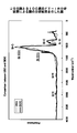
かかるレジスト膜のパターンの欠損を防ぐ方法として、Al配線パターンを形成する場合については、例えば、特開平11−97442号公報に、図1に示す構造及びプロセスが開示されている。
【0007】
図1(A)〜(B)は、前記従来技術の反射防止膜及び反応防止膜を用いた半導体装置の製造工程を示したものである。
【0008】
図1(A)に示すように、半導体基板1上に、シリコン酸化膜2と、アルミニウム配線3と、反射防止膜となるシリコン酸窒化膜4と、反応防止膜となるシリコン酸化膜5と、化学増幅型レジスト膜6とをまず順次形成する。
【0009】
シリコン酸窒化膜4を形成する目的は、定在波効果抑制のための反射防止膜である。しかし、シリコン酸窒化膜4自体は不安定であり、そのため大気中のアンモニア(NH3)やアミン(R−NH2)などの塩基物質がシリコン酸窒化膜4の表面に吸着し、化学増幅型レジスト膜6含まれている酸と中和反応を起こして、化学増幅型レジスト膜の酸反応を阻害して、化学増幅型レジスト6にパターンが形成されないという問題が発生する。
【0010】
そのため、化学的に安定した反応防止膜としてシリコン酸化膜2が、シリコン酸窒化膜4と、化学増幅型レジスト6との間に形成される。また、シリコン酸化膜2は、化学増幅型レジスト膜6との界面でのパターンの裾引きの発生を抑制している。
【0011】
先に述べたように、図1(B)に示すような、アルミニウム配線3上に、反射防止膜となるシリコン酸窒化膜4と、反応防止膜となるシリコン酸化膜5とを形成後に、化学増幅型レジスト膜6をパターニングすると定在波が抑制でき、それに加え、反射防止膜上に塩基性物質が吸着することが抑制できるため、レジストパターンの裾引きを抑制できると共に、定在波効果の少ない線幅制御性に優れたパターンを形成することができる。
【0012】
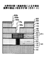
先にも説明したように、今日の半導体装置では、微細化、低消費電力化及び高速化等の要求に伴い、低誘電率層間絶縁膜の使用が検討されている。低誘電率層間絶縁膜への適用が期待される絶縁膜の一つとして、SiOC膜がある。
【0013】
SiOC膜はソースガスとして、Si(CH3)4, Si(CH3)3Hなどを用い、プラズマCVD法により成膜する低誘電率絶縁膜である。
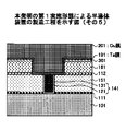
【0014】
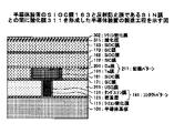
図2にUSG(非ドープシリケートガラス)膜とSiOC膜のFT−IR(フーリエ変換赤外吸収スペクトル)測定の結果を示す。
【0015】
図2を参照するに、SiOC膜は膜中に、C−H基と, Si−CH3基と, SiC基と, Si−OCH基とを含む酸化膜である。また、SiOC膜の膜密度は、1.3g/ccと低い。これに対し、USG膜はCVD法により形成された酸化膜であり、SiO結合のみが観測されている。USG膜は実質的にCなどのドーパントを含まないため、密度が高く、また誘電率も高い。
【0016】
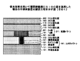
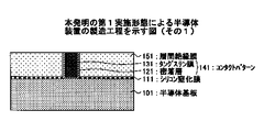
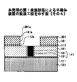
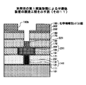
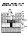
図3〜8は従来技術を用いて層間絶縁膜にSiOC膜を適用した場合の半導体装置の製造工程を示す。
【0017】
図3に示すように、半導体基板101上にシリコン窒化膜111と、層間絶縁膜151とを成膜後、図示していないコンタクトホール形成用の化学増幅型レジスト膜を層間絶縁膜151上にパターニングし、エッチングを行い、図示していない前記コンタクトホールを形成する。
【0018】
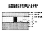
次に、図示していない前記コンタクトホール内部に、密着層121を前記コンタクトホールの内部形状に沿って形成し、さらにタングステン膜131を充填後、CMP法を用いて余分な密着層121とタングステン膜131とを除去し、コンタクトパターン141を形成する。次に、コンタクトパターン141上にシリコン窒化膜112と、SiOC膜161と、反射防止膜として使われるシリコン窒化膜301とを順次成膜する。次に、図示していない配線パターン形成用の化学増幅型レジスト膜を前記シリコン窒化膜301上に形成し、所望の配線パターンに対応した形状のレジスト窓を形成する。
【0019】
次に、前記化学増幅型レジスト膜をマスクにしてエッチングを行い、前記シリコン窒化膜301と、シリコン窒化膜112と、層間絶縁膜151中に、図示していない配線パターン用の溝を形成する。
【0020】
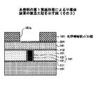
次に、前記配線パターン用の溝の内部に、Ta膜を溝形状に沿って形成し、さらにCu膜を、前記溝を充填するように成膜し、CMP法を用いて前記SiOC膜上の余分なTa膜とCu膜とを除去し、前記配線パターン用の溝の内部のみに、Ta膜とCu膜とよりなる配線パターン211を形成する。
【0021】
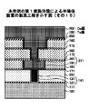
図3の工程では、次に配線パターン211上に、シリコン窒化膜113と、SiOC膜162と、シリコン窒化膜114と、SiOC膜163と、反射防止膜であるシリコン窒化膜302とを順次成膜する。
【0022】
次に、図4に示すように、反射防止膜としてのシリコン窒化膜302上にビアパターン形成用の化学増幅型レジスト膜182をパターニングして、レジスト窓182aを形成する。
【0023】
なお、図4中のレジスト窓182aのように、図中の壁を示すことによって空間全体を表すこととする。
【0024】
次に、図5に示すように、化学増幅型レジスト膜182をマスクにしてエッチングを行う。その結果、レジスト窓182aの形状は、SiOC膜162と、シリコン窒化膜114と、SiOC膜163と、反射防止膜であるシリコン窒化膜302とに転写され、対応した形状の開口部162aと、開口部114aと、開口部163aと、開口部302aとが形成される。
【0025】
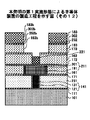
次に、図6に示すように、開口部162aのシリコン窒化膜113上に樹脂等よりなる保護膜221を形成する。
【0026】
次に、図7に示すように、反射防止膜としてのシリコン窒化膜302上に、形成したい配線パターンに対応したレジスト開口部183bを有する化学増幅型レジスト膜183を形成し、さらに図8の工程においてシリコン窒化膜302およびその下のSiOC膜163を、化学増幅型レジスト膜183をマスクにドライエッチングし、前記レジスト開口部183bに対応した配線溝パターンを形成する。
【0027】
さらに前記ビアパターン162aから前記保護膜221を除去し、Taなどのバリアメタル膜を形成した後、Cuなどの導体で前記配線溝パターンおよびビアパターンを充填し、さらに余分なバリアメタル膜およびCu層をCMP法により除去することにより、所望のビアコンタクトを有するCu配線パターンを形成することができる。
【0028】
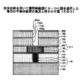
【発明が解決しようとする課題】
ところで、図7に示すように、反射防止膜としてのシリコン窒化膜302上に配線パターン形成用の化学増幅型レジスト膜183を形成した場合には、ビアパターン形成用ホール部の保護膜221上に、化学増幅型レジスト膜231が現像後も溶解されないで残ることがある。
【0029】
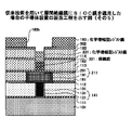
また図7に示した構造では、図8に示すように、溶解されないで残った化学増幅型レジスト膜231と接しているSiOC膜163、もしくは近傍のSiOC膜163が、配線パターン形成のためのエッチングを行った場合に、溶解されないで残った化学増幅型レジスト膜231によるシャドウイング効果により、SiOC膜163中にエッチング残渣241が、ビアパターン形成用ホール部の周りにスリーブ状に形成されて、配線パターン用の溝が形成できないという問題が発生することがある。
【0030】
そこで本発明は、上記事情に鑑みなされたもので、層間絶縁膜にSiOC膜を使用して、その上層に反射防止膜としてのシリコン窒化膜を形成し、デュアルダマシン法を適用した多層配線構造の半導体装置において、化学増幅型レジスト膜の溶解阻害現象を防止し、かつパターンの寸法精度に優れた半導体装置を提供することを課題とする。
【0031】
【課題を解決するための手段】
本発明は上記課題を、基板と、前記基板上に形成された多層配線構造とよりなる半導体装置であって、前記多層配線構造は、炭素を含むシリコン酸化膜からなる層間絶縁膜、前記層間絶縁膜上に形成された、窒素を含まない絶縁膜と、前記窒素を含まない絶縁膜上に形成された、窒素を含む絶縁膜とよりなることを特徴とする半導体装置により、解決する。
【0032】
上記構成において、前記層間絶縁膜は、多孔質絶縁膜により形成してもよい。前記絶縁膜はCVD酸化膜により形成してもよい。上記構成において、前記絶縁膜はTEOSガスを使った非ドープシリケート膜により形成してもよい。また、前記絶縁膜はSiC膜により形成してもよい。さらに、前記絶縁膜はリンドープシリケート膜により形成してもよい。前記絶縁膜は、前記層間絶縁膜よりも高密度のSiOC膜により形成してもよい。
【0033】
上記構成において、前記絶縁膜は、膜厚が100nm以下に形成してもよい。また、前記絶縁膜は、膜厚が30nm以下に形成してもよい。
【0034】
上記構成において、前記層間絶縁膜中には、導体により充填された配線溝が形成されており、前記基板と前記層間絶縁膜との間には別の層間絶縁膜が形成されており、前記別の層間絶縁膜中には、前記導体により充填され前記配線溝から延在するビアコンタクトが形成されるようにしてもよい。
【0035】
また、本発明は上記課題を、多層配線構造を有する半導体装置の製造方法であって、基板上に炭素を含む酸化膜よりなる層間絶縁膜を形成する工程と、前記層間絶縁膜上に、窒素を含まないガスにより、絶縁膜を形成する工程と、前記絶縁膜上に反射防止膜を形成する工程と、前記反射防止膜上に化学増幅型レジスト膜を形成する工程と、前記化学増幅型レジスト膜をパターニングする工程とを含むことを特徴とする半導体装置の製造方法により、解決する。
【0036】
また、本発明は上記課題を、基板上に第1の層間絶縁膜を形成する工程と、前記第1の層間絶縁膜上に炭素を含むシリコン酸化膜よりなる第2の層間絶縁膜を形成する工程と、前記第2の層間絶縁膜上に絶縁膜を形成する工程と、前記絶縁膜上に反射防止膜を形成する工程と、前記第1および第2の層間絶縁膜中に、前記第1の開口部を形成する工程と、前記第2の層間絶縁膜中に、前記反射防止膜上に形成された化学増幅型レジスト膜をマスクに、第2の開口部を形成する工程とよりなり、前記絶縁膜は、窒素を含まないガスにより形成されることを特徴とする半導体装置の製造方法により、解決する。
上記構成において、前記第1および第2の層間絶縁膜は、いずれも炭素を含むシリコン酸化膜より形成してもよい。また、前記炭素を含むシリコン酸化膜は多孔質膜により形成してもよい。前記絶縁膜は、TEOSガスを使ったCVD法により形成してもよい。前記絶縁膜は、成長ガスとしてTetramethylsilane{Si(CH3)4}と、CO2とを用いたSiC膜により形成してもよい。また、前記絶縁膜は、PSG膜により形成してもよい。さらに、前記絶縁膜は、成長ガスとしてTetramethelcyclotetrasiloxane{CH3(H)SiO4}と、CO2と、O2とを用いた前記層間絶縁膜よりも高密度のSiOC膜により形成してもよい。
上記構成において、前記反射防止膜は、成長ガスとしてSiH4と、NH3と、N2とを用いたSiN膜により形成してもよい。前記絶縁膜は、膜厚が100nm以下に形成してもよい。さらに、前記絶縁膜は、膜厚が30nm以下に形成してもよい。
(作用)
本発明によれば、炭素を含むシリコン酸化膜からなる前記層間絶縁膜と、窒素を含む前記絶縁膜との間に、窒素を含まない前記絶縁膜を形成することにより、窒素を含む前記絶縁膜の成膜中に発生する窒素ガスの、炭素を含むシリコン酸化膜からなる前記層間絶縁膜中への拡散を防ぎ、前記窒素ガスと前記層間絶縁膜にあるH基との反応によるNHなどのアミン基が前記層間絶縁膜中での生成されることを防ぐことができる。そのため、前記層間絶縁膜に接する化学増幅型レジスト膜の溶解阻害現象を防ぐことができ、多層配線構造の半導体装置の良好なパターニングを行うことができる。
【0037】
化学増幅型レジスト膜(ポジ型)は、露光により酸を発生し、露光後の熱処理により反応生成物の極性を変化させる化合物を含んでいる。そこで発生した酸の触媒反応により極性化が起こり、化学増幅型レジスト膜が現像液に対する溶解性を有するようになり、パターニングがなされる。また化学増幅型レジスト膜(ネガ型)は、露光後の熱処理により反応生成物を架橋する化合物を含み、発生した酸の触媒反応により架橋され、レジスト膜が現像液に対して固定することになり、パターニングされる。
【0038】
したがって、図7,8におけるような化学増幅型レジスト膜231の溶解阻害現象は、酸反応が阻害されたことで発生したものと考えられる。つまり、図7に示した半導体装置の構造において、化学増幅型レジスト膜231へのアルカリ物質供給による中和反応が発生したと考えられる。
【0039】
SiC膜と、SiOC膜と、反射防止膜としてのシリコン窒化膜の成長ガスを比較すると、SiC膜の成長ガスは、Tetramethylsilane{Si(CH3)4}と、CO2が使われており、SiOC膜の成長ガスには、Tetramethelcyclotetrasiloxane{CH3(H)SiO4}と、CO2と、O2が使われており、また反射防止膜としてのシリコン窒化膜の成長ガスには、SiH4と、NH3と、N2が使われている。
【0040】
そこで上記成長ガスと図7に示した半導体装置の構造において、化学増幅型レジスト膜231の溶解阻害現象を考察するに、反射防止膜としてのシリコン窒化膜302の成膜中に発生するNH3の分解、もしくは、N2が反射防止膜としてのシリコン窒化膜302の下層に形成されたSiOC膜163中に拡散して、SiOC膜163中のH基と反応し、NH等のアミン基がSiOC膜163中で生成される機構が考えられる。このようにして生成したアミン基は、ビアホール内の保護膜221上に形成された化学増幅型レジスト膜231に供給され、化学増幅型レジスト膜231の酸反応を阻害することにより前記化学増幅型レジスト膜231の溶解阻害現象が発生したと考えられる。
【0041】
層間絶縁膜にSiOC膜を使用し、その上層に反射防止膜としてシリコン窒化膜を形成し、デュアルダマシン法を用いて多層配線構造の半導体装置を作成する場合には、従来技術の方法では、図7に示したSiOC膜163上にシリコン窒化膜302が反射防止膜として形成されるが、シリコン窒化膜302中には窒素(N)が含まれており、前記窒素がSiOC膜163中のH基と反応すると、NH等のアミン基がSiOC膜163中で生成される。このようにして形成されたアミン基が前記ビアホール内の化学増幅型レジスト膜231に供給されると、光酸を中和してしまい、酸反応の阻害現象を生るものと考えられる。
【0042】
次に、本発明の発明者が本発明の基礎となる研究において、デュアルダマシン構造を形成する領域の層間絶縁膜と、ストッパー兼拡散防止膜の組み合わせを様々に変化させ、最上層の層間絶縁膜上に反射防止膜としてのシリコン窒化膜を形成し、ビアホール内の保護膜上の化学増幅レジスト膜が溶解阻害現象を受けるか否かについて実験を行った結果を示す。
【0043】
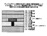
図9は、デュアルダマシン構造を形成する領域に層間絶縁膜としてUSG膜と、ストッパー兼拡散防止膜としてシリコン窒化膜を積層させた半導体装置の構造を示す。
【0044】
半導体基板101上にシリコン窒化膜111と、USG膜251とを成膜後に、図示していないコンタクトホール形成用の化学増幅型レジスト膜を層間絶縁膜251上にパターニングし、エッチングを行い、前記コンタクトホールを形成する。
【0045】
次に、前記コンタクトホール内部に、密着層121と、タングステン膜131とを成膜後、CMP法を用いて前記コンタクトホール以外の密着層121と、タングステン膜131とを除去してコンタクトパターン141を形成する。
【0046】
次に、コンタクトパターン141上にシリコン窒化膜112と、USG膜252と、図示していない反射防止膜としてのSiN膜を成膜する。次に、図示していない配線パターン形成用の化学増幅型レジスト膜を図示していない前記反射防止膜としてのシリコン窒化膜上にパターニングする。次に、図示していない前記配線パターン形成用の化学増幅型レジスト膜をマスクにしてエッチングを行い、図示していない前記反射防止膜としてのシリコン窒化膜と、シリコン窒化膜112と、USG膜252との膜中に、図示していない配線パターン用の溝を形成する。次に、図示していない前記配線パターン用の溝の内部に、Ta膜191と、Cu膜201とを成膜して、CMP法を用いて前記配線パターン用の溝の内部のみに、Ta膜191と、Cu膜201とを残して配線パターン211を形成する。
【0047】
次に、配線パターン211上に、シリコン窒化膜113と、USG膜253と、シリコン窒化膜114と、USG膜254と、反射防止膜としてのシリコン窒化膜302とを成膜する。
【0048】
このような図9に示した半導体装置の構造において、先に述べた図4〜8に示した工程と同様にデュアルダマシン構造を形成したところ、先に説明したような化学増幅型レジスト膜の溶解阻害現象は発生しなかった。
【0049】
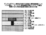
図10は、デュアルダマシン構造を形成する領域に層間絶縁膜としてFSG膜と、ストッパー兼拡散防止膜としてシリコン窒化膜を積層させた半導体装置の構造を示したものである。
【0050】
コンタクトパターン形成までの工程は、先に説明した図9と同様であるので対応する参照符号を付し、説明を省略する。
【0051】
コンタクトパターン141形成後に、コンタクトパターン141上にシリコン窒化膜112と、FSG膜261と、図示していない反射防止膜としてのシリコン窒化膜を成膜する。次に、図示していない配線パターン形成用の化学増幅型レジスト膜を、図示していない前記反射防止膜としてのシリコン窒化膜上にパターニングする。次に、図示していない前記配線パターン形成用の化学増幅型レジスト膜をマスクにしてエッチングを行い、図示していない前記反射防止膜としてのSiN膜と、シリコン窒化膜112と、FSG膜261との膜中に、図示していない配線パターン用の溝を形成する。次に、図示していない前記配線パターン用の溝の内部に、Ta膜191と、Cu膜201とを成膜して、CMP法を用いて前記配線パターン用の溝の内部のみに、Ta膜191と、Cu膜201とを残して配線パターン211を形成する。
【0052】
次に、配線パターン211上に、シリコン窒化膜113と、FSG膜262と、シリコン窒化膜114と、FSG膜263と、反射防止膜としてのシリコン窒化膜302とを成膜する。
【0053】
このような図10に示した半導体装置の構造において、先に述べた図4〜8に示した工程と同様にデュアルダマシン構造を形成した場合ところ、化学増幅型レジスト膜の溶解阻害現象は発生しないことが確認された。
【0054】
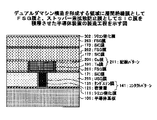
図11は、デュアルダマシン構造を形成する領域に層間絶縁膜としてFSG膜と、ストッパー兼拡散防止膜としてSiC膜を積層させた半導体装置の構造を示したものである。
【0055】
コンタクトパターン形成までの工程は、先に説明した図9と同様であるので対応する参照符号を付し、説明を省略する。
【0056】
コンタクトパターン141形成後に、コンタクトパターン141上にSiC膜171と、FSG膜261と、図示していない反射防止膜としてのシリコン窒化膜を成膜する。次に、図示していない配線パターン形成用の化学増幅型レジスト膜を、図示していない前記反射防止膜としてのシリコン窒化膜上にパターニングする。次に、図示していない前記配線パターン形成用の化学増幅型レジスト膜をマスクにしてエッチングを行い、図示していない前記反射防止膜としてのシリコン窒化膜と、SiC膜171と、FSG膜261との膜中に、図示していない配線パターン用の溝を形成する。次に、図示していない前記配線パターン用の溝の内部に、Ta膜191と、Cu膜201とを成膜して、CMP法を用いて前記配線パターン用の溝の内部のみに、Ta膜191と、Cu膜201とを残して配線パターン211を形成する。
【0057】
次に、配線パターン211上に、SiC膜172と、FSG膜262と、SiC膜173と、FSG膜263と、反射防止膜としてのシリコン窒化膜302とを成膜する。
【0058】
このような図11に示した半導体装置の構造において、先に述べた図4〜8に示した工程と同様にデュアルダマシン構造を形成したところ、図示していない化学増幅型レジスト膜の溶解阻害現象は発生しなかった。
【0059】
以上、図9〜11に示した層間絶縁膜と、ストッパー兼拡散防止と、反射防止膜であるシリコン窒化膜の組み合わせにおいては、図示していない化学増幅型レジスト膜の溶解阻害現象は発生しないことが確認できた。
【0060】
次に層間絶縁膜にSiOC膜を用いて、SiOC膜上に反射防止膜であるシリコン窒化膜を成膜した半導体装置と、成膜しない半導体装置とにおいて、デュアルダマシン構造を形成する実験を行った。
【0061】
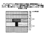
図12は、デュアルダマシン構造を形成する領域に層間絶縁膜としてSiOC膜と、ストッパー兼拡散防止膜としてSiC膜を積層させた半導体装置の構造を示したものである。
【0062】
コンタクトパターン形成までの工程は、先に説明した図9と同様であるので対応する参照符号を付し、説明を省略する。
【0063】
コンタクトパターン141形成後に、コンタクトパターン141上にSiC膜171と、SiOC膜161と、図示していない反射防止膜としてのシリコン窒化膜を成膜する。次に、図示していない配線パターン形成用の化学増幅型レジスト膜を、図示していない前記反射防止膜としてのシリコン窒化膜上にパターニングする。次に、図示していない前記配線パターン形成用の化学増幅型レジスト膜をマスクにしてエッチングを行い、図示していない前記反射防止膜としてのシリコン窒化膜と、SiC膜171と、SiOC膜161との膜中に、図示していない配線パターン用の溝を形成する。次に、図示していない前記配線パターン用の溝の内部に、Ta膜191と、Cu膜201とを成膜して、CMP法を用いて前記配線パターン用の溝の内部のみに、Ta膜191と、Cu膜201とを残して配線パターン211を形成する。
【0064】
次に、配線パターン211上に、SiC膜172と、SiOC膜162と、SiC膜173と、SiOC膜163とを成膜する。
【0065】
このような図12に示した半導体装置の構造において、先に述べた図4〜8に示した工程と同様にデュアルダマシン構造を形成したところ、図示していない化学増幅型レジスト膜の溶解阻害現象は発生しなかった。
【0066】
図13は、デュアルダマシン構造を形成する領域に層間絶縁膜としてSiOC膜と、ストッパー兼拡散防止膜としてSiC膜を積層させて、最上層のSiOC膜上に反射防止膜としてのシリコン窒化膜を形成した半導体装置の構造を示したものである。
【0067】
図13は、図12に示した半導体装置の構造に形成した後に、SiOC膜163上に反射防止膜としてのシリコン窒化膜302を形成した半導体装置である。
【0068】
図13中に、先に説明した部分に対応する部分には同一の参照符号を付し、説明を省略する。
【0069】
このような図13に示した半導体装置の構造において、先に述べた図4〜8に示した工程と同様にデュアルダマシン構造を形成したところ、図示していない化学増幅型レジスト膜の溶解阻害現象が発生するのが確認された。
【0070】
したがって、図9〜13の構造の半導体装置の実験結果から、多層配線構造の半導体装置において、層間絶縁膜にSiOC膜を使用し、前記SiOC膜上に反射防止膜としてのシリコン窒化膜を形成した後に、デュアルダマシン構造を形成する場合には化学増幅型レジスト膜の溶解阻害現象が発生することが分かった。これは、先に述べたように、反射防止膜としてのシリコン窒化膜302の成膜中に発生するN2が、反射防止膜としてのシリコン窒化膜302の下層に形成されたSiOC膜163中に拡散して、SiOC膜163中のH基と反応し、NH等のアミン基がSiOC膜163中で生成され、前記アミン基がビアホール内の保護膜221上に形成された化学増幅型レジスト膜231に供給されて、化学増幅型レジスト膜231の酸反応が阻害すされたためと考えられる。
【0071】
図14は、図13に示した半導体装置のSiOC膜163と反射防止膜であるSiN膜との間に酸化膜311を形成した半導体装置の構造を示したものである。
【0072】
図14中の酸化膜311は、シリコン窒化膜302の成膜中に発生するN2が、SiOC膜163に拡散するのを防ぎ、SiOC膜163中のアミン基の生成を防ぐための拡散防止膜である。
【0073】
図15に、酸化膜311として、SiH4系USG膜(屈折率1.47)の膜厚が50nmと、SiH4系USG膜(屈折率1.47)の膜厚が100nmの膜と、SiH4系USG膜(屈折率1.51)の膜厚が100nmと、TEOS系USG膜(屈折率1.46)の膜厚が30nmの膜と、TEOS系USG膜(屈折率1.46)の膜厚が30nmの膜とを、それぞれ形成して先に述べた図4〜8に示した工程と同様にデュアルダマシン構造を形成した場合に、図示していない化学増幅型レジスト膜の溶解阻害現象の発生の有無を確認した結果を示す。
【0074】
前記SiH4系USG膜(屈折率1.47)と前記SiH4系USG膜(屈折率1.51)の成長ガスには、SiH4と、N2Oと、N2とを用いた。TEOS系USG膜(屈折率1.46)の成長ガスには、TEOS{Tetraethoxysilane,Si(OC2H5)4}と、O2とを用いた。
【0075】
すなわち、図15は、層間絶縁膜であるSiOC膜と反射防止膜としてのシリコン窒化との間に形成した絶縁膜の種類と膜厚による、化学増幅型レジスト膜の溶解阻害現象の発生の有無を確認した実験結果である。
【0076】
図15から、前記SiH4系USG膜(屈折率1.47)と前記SiH4系USG膜(屈折率1.51)については、図示していない化学増幅型レジスト膜の溶解阻害現象が生じるのがみられた。
【0077】
これは、SiH4系USG膜の成長ガスの中に含まれるN2OまたはN2が、SiOC膜163に拡散して、SiOC膜163中にアミン基が生成され、図示していない化学増幅型レジスト膜に供給されて、図示していない化学増幅型レジスト膜の酸反応が阻害されたためと考えられる。これに対し、TEOS系USG膜(屈折率1.46)の成長ガスには、N2OまたはN2が含まれておらず、拡散防止膜としての機能を果せたために、図示していない化学増幅型レジスト膜の溶解阻害現象が発生しなかったと考えられる。
【0078】
このことから、半導体装置において、SiOC膜上に反射防止膜としてのSiN膜を形成してパターニングを行う場合には、前記SiOC膜と反射防止膜としてのSiN膜との間に、成長ガスにNを含まない膜、例えば、TEOS系USG膜を形成後に、デュアルダマシン構造を形成することが望ましく、その膜厚は30nm程度で十分である。
【0079】
【発明の実施の形態】
以下、図面に基づいて本発明の実施例を説明する。
(第1の実施形態)
図16〜31は、デュアルダマシン法と反射防止膜を用いて層間絶縁膜であるSiOC膜をパターニングする本発明の第1実施形態による半導体装置の製造工程を示す。
【0080】
コンタクトパターンの形成工程
図16を参照するに、図示していない回路素子を半導体基板上101に形成した後、半導体基板101上に、シリコン窒化膜111とシリコン酸化膜151とを成膜し、図示していない前記回路素子部を平坦化するために、CMP法を用いてシリコン酸化膜151の研磨を行う。その後、シリコン酸化膜151上に、図示していないコンタクトパターン形成用の化学増幅型レジスト膜のパターニングを行い、前記、化学増幅型レジスト膜をマスクにしてエッチングを行い、図示していないコンタクトホールを形成する。次に、密着層121と、タングステン膜131とを前記コンタクトホール内に成膜し、CMP法を用いて前記コンタクトホール内のみに密着層121と、タングステン膜131とを残し、コンタクトパターン141を形成する。
【0081】
層間絶縁膜の形成工程
次に、図17の工程において、コンタクトパターン141上にシリコン窒化膜112と、SiOC膜161と、反射防止膜としてのシリコン窒化膜301とを成膜する。
【0082】
SiOC膜のソースガスには、Si(CH3)4, Si(CH3)3Hなどを用い、プラズマCVD法により形成される。実際のプロセス例としては、例えば、Novellus社のConcept Two Sequelを用い、使用ガスとしてはCH3(H)SiO4, CO2, O2を用いたものがある。USG膜とは違い、SiOC膜はC−H,Si−CH3, Si−C, Si−OCH基を含む膜である。
【0083】
配線パターン形成用化学増幅型レジスト膜のパターニング工程
次に、図18の工程において、反射防止膜としてのシリコン窒化膜301上に配線パターン形成のための化学増幅型レジスト膜181をパターニングして、開口部181aを形成する。
【0084】
配線パターン用溝形成の工程
次に、図19の工程において、化学増幅型レジスト膜181をマスクにして、シリコン窒化膜112と、SiOC膜161と、反射防止膜としてのシリコン窒化膜301とをエッチングを行い、開口部181aを転写して、シリコン窒化膜112中に開口部112aと、SiOC膜161中に開口部161aと、反射防止膜としてのシリコン窒化膜301中に開口部301aとを形成する。
【0085】
配線パターン用材料の成膜の工程
次に、図20の工程において、シリコン窒化膜112中の開口部112aと、SiOC膜161中の開口部161aと、反射防止膜としてのシリコン窒化膜301中の開口部301aとの内部に、Ta膜と、Cu膜とを成膜する。
【0086】
CMP法による配線パターン形成の工程
次に、図21の工程において、図20に示した構造の半導体装置の研磨を行い、配線パターン211を形成する。
【0087】
デュアルダマシン形成用の層間絶縁膜成膜の工程
次に、図22の工程において、配線パターン211上に、SiC膜172と、SiOC膜162と、SiC膜173と、SiOC膜163と、拡散防止膜としてのUSG膜252と、反射防止膜としてのシリコン窒化膜302とを形成する。
【0088】
USG膜252は、例えば、成長ガスにN2OまたはN2が含まれていないTEOS系USG膜を厚さ30nmで成膜する。また、成長ガスにN2OまたはN2が含まれていない膜であればUSG膜以外でも、反射防止膜としてのシリコン窒化膜302中に含まれるN2がSiOC膜163中に拡散することを防ぎ、SiOC膜163中においてアミン基が生成されることを防ぐ拡散防止膜の機能を果たす。
【0089】
ビアパターン形成用の化学増幅型レジスト膜形成の工程
次に、図23の工程において、反射防止膜としてのSiN膜302上に、配線パターン211と導通をとるためのビアパターン形成用の化学増幅レジスト膜182をパターニングして、開口部182aを形成する。
【0090】
ビアパターン形成用エッチングの工程
次に、図24の工程において、化学増幅レジスト膜182をマスクにしてエッチングを行い、開口部182aを転写して、SiOC膜162中に開口部162aと、SiC膜173中に開口部173aと、SiOC膜163中に開口部163aと、USG膜252中に開口部252aと、反射防止膜としてのシリコン窒化膜302中に開口部302aとを形成する。
【0091】
保護膜の形成の工程
次に、図25の工程において、SiC膜172上にエッチング時のSiC膜172の保護するものとして樹脂系の材料の保護膜221を形成する。
【0092】
配線パターン形成用化学増幅型レジスト膜のパターニング工程
次に、図26の工程において、反射防止膜としてのシリコン窒化膜302上に配線パターン形成のための化学増幅型レジスト膜183をパターニングして、開口部183b形成する。
【0093】
配線パターン用溝形成の工程
次に、図27の工程において、化学増幅型レジスト膜183をマスクとしてSiOC膜163と、拡散防止膜としてのUSG膜252と、反射防止膜としてのシリコン窒化膜302とをエッチングして、開口部183bを転写し、SiOC膜163中に開口部163bと、拡散防止膜としてのUSG膜252中に開口部252bと、反射防止膜としてのシリコン窒化膜302中に開口部302bとを形成する。
【0094】
次に、図28の工程において、残った化学増幅型レジスト膜183と、保護膜221をアッシングにより除去する。
【0095】
次に、図29の工程において、USG膜252上にある反射防止膜としてのSiN膜302と、SiC膜173と、SiC膜172とをエッチングして、SiC膜173中に開口部173bと、SiC膜172中に開口部172aとを形成する。 SiC膜173は、USG膜252中の開口部252bがマスクとなりエッチングされる。また、SiC膜172については、SiOC膜162中の開口部162aがマスクとなりエッチングされる。
【0096】
配線パターン用材料の成膜の工程
次に、図30の工程において、図29に示した開口部252bと、開口部163bと、開口部173bと、開口部162aと、開口部172aとの内部に、Ta膜192と、Cu膜202を成膜する。
【0097】
CMP法による配線パターン及びビアパターンの形成
次に、図31の工程においてCMP法を用いて研磨を行い、その後、USG膜252と、配線パターン212上に拡散防止膜としてのSiC膜を形成する。
【0098】
このように、SiOC膜を用いたデュアルダマシン構造の半導体装置において、反射防止膜を用いてSiOC膜をパターニングしていく場合には、SiOC膜と反射防止膜としてのシリコン窒化膜との間に、成長ガスにNを含まない膜、例えば、TEOS系USG膜を形成後に、デュアルダマシン構造を形成することが、化学増幅型レジスト膜の溶解阻害現象を防ぐのに有効である。また、前記TEOS系USG膜の膜厚は30nmで十分である。
(第2の実施形態)
本発明に係る半導体装置の製造方法の第1の実施例では、拡散防止膜としてのUSG膜252を、SiOC膜163と、反射防止膜としてのシリコン窒化膜302との間に形成した例を示したが、USG膜252の代わりに、成長ガスにNを含まないSiC膜を形成してもよい。
【0099】
SiC膜の成長ガスは、先に述べたようにTetramethylsilane{Si(CH3)4}と、CO2が用いられる。
【0100】
SiOC膜163上に拡散防止膜としてのSiC膜を形成し、SiC膜上に反射防止膜としてのシリコン窒化膜302を形成する構造により、反射防止膜としてのシリコン窒化膜302の成膜中に発生するN2ガスが、反射防止膜としてのシリコン窒化膜302の下層に形成されたSiOC膜163中への拡散が防ぐことができ、前記N2ガスがSiOC膜163中のH基と反応し、NH等のアミン基がSiOC膜163中で生成されることを防ぐことができ、化学増幅型レジスト膜の溶解阻害現象の防止が可能である。
(第3の実施形態)
本発明に係る半導体装置の製造方法の第1の実施例では、拡散防止膜としてのUSG膜252を、SiOC膜163と、反射防止膜としてのシリコン窒化膜302との間に形成した例を示したが、USG膜252の代わりに、成長ガスにNを含まないPSG膜を形成してもよい。
【0101】
PSG膜の成長ガスには、PH3,O2,He等、もしくは、PO(OC2H5)3,O3,O2,He,N2等が用いられる。
【0102】
SiOC膜163上に拡散防止膜としてのPSG膜を形成し、PSG膜上に反射防止膜としてのシリコン窒化膜302を形成する構造により、反射防止膜としてのシリコン窒化膜302の成膜中に発生するN2ガスが、反射防止膜としてのSiN膜302の下層に形成されたSiOC膜163中への拡散が防ぐことができ、前記N2ガスがSiOC膜163中のH基と反応し、NH等のアミン基がSiOC膜163中で生成されることを防ぐことができ、化学増幅型レジスト膜の溶解阻害現象の防止が可能である。
(第4の実施形態)
本発明に係る半導体装置の製造方法の第1の実施例では、拡散防止膜としてのUSG膜252を、SiOC膜163と、反射防止膜としてのシリコン窒化膜302との間に形成した例を示したが、USG膜252の代わりに、成長ガスにNを含まなくて、かつ、前記SiOC膜163よりも膜密度の高いSiOC膜を形成してもよい。
【0103】
SiOC膜の成長ガスは、先に述べたようにTetramethelcyclotetrasiloxane{CH3(H)SiO4}と、CO2と、O2が用いられる。
【0104】
SiOC膜163上に拡散防止膜としての膜密度の高いSiOC膜を形成し、前記膜密度の高いSiOC膜上に反射防止膜としてのシリコン窒化膜302を形成する構造により、反射防止膜としてのシリコン窒化膜302の成膜中に発生するN2ガスが、反射防止膜としてのシリコン窒化膜302の下層に形成されたSiOC膜163中への拡散が防ぐことができ、前記N2ガスがSiOC膜163中のH基と反応し、NH等のアミン基がSiOC膜163中で生成されることを防ぐことができ、化学増幅型レジスト膜の溶解阻害現象の防止が可能である。
以上、本発明の好ましい実施例について詳述したが、本発明はかかる特定の実施形態に限定されるものではなく、特許請求の範囲内に記載された本発明の要旨の範囲内において、種々の変形・変更が可能である。
【0105】
(付記1) 基板と、
前記基板上に形成された多層配線構造とよりなる半導体装置であって、
前記多層配線構造は、炭素を含むシリコン酸化膜からなる層間絶縁膜、
前記層間絶縁膜上に形成された、窒素を含まない絶縁膜と、
前記窒素を含まない絶縁膜上に形成された、窒素を含む絶縁膜とよりなることを特徴とする半導体装置。
【0106】
(付記2) 前記層間絶縁膜は、多孔質絶縁膜よりなることを特徴とする付記1記載の半導体装置。
【0107】
(付記3) 前記絶縁膜はCVD酸化膜であることを特徴とする付記1または2記載の半導体装置。
【0108】
(付記4) 前記絶縁膜はTEOSガスを使った非ドープシリケート膜であることを特徴とする付記1〜3のうち、いずれか一項記載の半導体装置。
【0109】
(付記5) 前記絶縁膜はSiC膜であることを特徴とする請求項1または2記載の半導体装置。
【0110】
(付記6) 前記絶縁膜はリンドープシリケート膜であることを特徴とする付記1または2記載の半導体装置。
【0111】
(付記7) 前記絶縁膜は、前記層間絶縁膜よりも高密度のSiOC膜であることを特徴とする付記1または2記載の半導体装置。
【0112】
(付記8) 前記絶縁膜は、膜厚が100nm以下であることを特徴とする付記1または2記載の半導体装置。
【0113】
(付記9) 前記絶縁膜は、膜厚が30nm以下であることを特徴とする付記1または2記載の半導体装置。
【0114】
(付記10) 前記層間絶縁膜中には、導体により充填された配線溝が形成されており、
前記基板と前記層間絶縁膜との間には別の層間絶縁膜が形成されており、前記別の層間絶縁膜中には、前記導体により充填され前記配線溝から延在するビアコンタクトが形成されていることを特徴とする付記1〜7のうち、いずれか一項記載の半導体装置。
【0115】
(付記11) 多層配線構造を有する半導体装置の製造方法であって、
基板上に炭素を含む酸化膜よりなる層間絶縁膜を形成する工程と、
前記層間絶縁膜上に、窒素を含まないガスにより、絶縁膜を形成する工程と、
前記絶縁膜上に反射防止膜を形成する工程と、
前記反射防止膜上に化学増幅型レジスト膜を形成する工程と、
前記化学増幅型レジスト膜をパターニングする工程とを含むことを特徴とする半導体装置の製造方法。
【0116】
(付記12) 基板上に第1の層間絶縁膜を形成する工程と、
前記第1の層間絶縁膜上に炭素を含むシリコン酸化膜よりなる第2の層間絶縁膜を形成する工程と、
前記第2の層間絶縁膜上に絶縁膜を形成する工程と、
前記絶縁膜上に反射防止膜を形成する工程と、
前記第1および第2の層間絶縁膜中に、前記第1の開口部を形成する工程と、
前記第2の層間絶縁膜中に、前記反射防止膜上に形成された化学増幅型レジスト膜をマスクに、第2の開口部を形成する工程とよりなり、
前記絶縁膜は、窒素を含まないガスにより形成されることを特徴とする半導体装置の製造方法。
【0117】
(付記13) 前記第1および第2の層間絶縁膜は、いずれも炭素を含むシリコン酸化膜よりなることを特徴とする付記12記載の半導体装置の製造方法。
【0118】
(付記14) 前記炭素を含むシリコン酸化膜は多孔質膜であることを特徴とする付記12または13のうちいずれか一項記載の半導体装置の製造方法。
【0119】
(付記15) 前記絶縁膜は、TEOSガスを使ったCVD法により形成されることを特徴とする付記12〜14のうち、いずれか一項記載の半導体装置の製造方法。
【0120】
(付記16) 前記絶縁膜は、成長ガスとしてTetramethylsilane{Si(CH3)4}と、CO2とを用いたSiC膜により形成されることを特徴とする付記12〜14のうち、いずれか一項記載の半導体装置の製造方法。
【0121】
(付記17) 前記絶縁膜は、PSG膜により形成されることを特徴とする付記12〜14のうち、いずれか一項記載の半導体装置の製造方法。
【0122】
(付記18) 前記絶縁膜は、成長ガスとしてTetramethelcyclotetrasiloxane{CH3(H)SiO4}と、CO2と、O2とを用いた前記層間絶縁膜よりも高密度のSiOC膜により形成されることを特徴とする付記12〜14のうち、いずれか一項記載の半導体装置の製造方法。
【0123】
(付記19) 前記反射防止膜は、成長ガスとしてSiH4と、NH3と、N2とを用いたSiN膜により形成されることを特徴とする付記12〜14のうち、いずれか一項記載の半導体装置の製造方法。
【0124】
(付記20) 前記絶縁膜は、膜厚が100nm以下に形成されることを特徴とする付記12〜18記載の半導体装置の製造方法。
【0125】
(付記21) 前記絶縁膜は、膜厚が30nm以下に形成されることを特徴とする付記12〜18記載の半導体装置の製造方法。
【0126】
【発明の効果】
本発明によれば、層間絶縁膜であるSiOC膜と、反射防止膜である窒素を含む絶縁膜、例えばシリコン窒化膜との間に、USG膜などの窒素を含まない絶縁膜を形成することにより、前記シリコン窒化膜の成膜時に使用するN2ガスが、前記SiOC膜中へ拡散することを防ぐことができ、前記N2ガスがSiOC膜163中のH基と反応し、NH等のアミン基がSiOC膜163中で生成されることを防ぐことができる。そのため、化学増幅型レジスト膜の溶解阻害現象の防止が可能となり、多層配線構造の半導体装置の良好なパターニングが形成できる。
【図面の簡単な説明】
【図1】図1(A)〜(B)は、従来技術の反射防止膜及び反応防止膜を用いた半導体装置の製造工程を示す図である。
【図2】図2は、USG膜とSiOC膜のFT−IR分析装置による膜の分析結果を示した図である。
【図3】図3は、従来技術を用いて層間絶縁膜にSiOC膜を適用した場合の半導体装置の製造工程を示す図(その1)である。
【図4】図4は、従来技術を用いて層間絶縁膜にSiOC膜を適用した場合の半導体装置の製造工程を示す図(その2)である。
【図5】図5は、従来技術を用いて層間絶縁膜にSiOC膜を適用した場合の半導体装置の製造工程を示す図(その3)である。
【図6】図6は、従来技術を用いて層間絶縁膜にSiOC膜を適用した場合の半導体装置の製造工程を示す図(その4)である。
【図7】図7は、従来技術を用いて層間絶縁膜にSiOC膜を適用した場合の半導体装置の製造工程を示す図(その5)である。
【図8】図8は、従来技術を用いて層間絶縁膜にSiOC膜を適用した場合の半導体装置の製造工程を示す図(その6)である。
【図9】図9は、デュアルダマシン構造を形成する領域に層間絶縁膜としてUSG膜と、ストッパー兼拡散防止膜としてSiN膜を積層させた半導体装置の製造工程を示す図である。
【図10】図10は、デュアルダマシン構造を形成する領域に層間絶縁膜としてFSG膜と、ストッパー兼拡散防止膜としてSiN膜を積層させた半導体装置の製造工程を示す図である。
【図11】図11は、デュアルダマシン構造を形成する領域に層間絶縁膜としてFSG膜と、ストッパー兼拡散防止膜としてSiC膜を積層させた半導体装置の製造工程を示す図である。
【図12】図12は、デュアルダマシン構造を形成する領域に層間絶縁膜としてSiOC膜と、ストッパー兼拡散防止膜としてSiC膜を積層させた半導体装置の製造工程を示す図である。
【図13】図13は、デュアルダマシン構造を形成する領域に層間絶縁膜としてSiOC膜と、ストッパー兼拡散防止膜としてSiC膜を積層させて、最上層のSiOC膜上に反射防止膜としてのSiN膜を形成した
【図14】図14は、半導体装置のSiOC膜163と反射防止膜であるSiN膜との間に酸化膜311を形成した半導体装置の製造工程を示す図である。
【図15】図15は、層間絶縁膜であるSiOC膜と反射防止膜としてのシリコン窒化との間に形成した絶縁膜の種類と膜厚による、化学増幅型レジスト膜の溶解阻害現象の発生の有無を確認した実験結果である。
【図16】図16は、本発明の第1実施形態による半導体装置の製造工程を示す図(その1)である。
【図17】図17は、本発明の第1実施形態による半導体装置の製造工程を示す図(その2)である。
【図18】図18は、本発明の第1実施形態による半導体装置の製造工程を示す図(その3)である。
【図19】図19は、本発明の第1実施形態による半導体装置の製造工程を示す図(その4)である。
【図20】図20は、本発明の第1実施形態による半導体装置の製造工程を示す図(その5)である。
【図21】図21は、本発明の第1実施形態による半導体装置の製造工程を示す図(その6)である。
【図22】図22は、本発明の第1実施形態による半導体装置の製造工程を示す図(その7)である。
【図23】図23は、本発明の第1実施形態による半導体装置の製造工程を示す図(その8)である。
【図24】図24は、本発明の第1実施形態による半導体装置の製造工程を示す図(その9)である。
【図25】図25は、本発明の第1実施形態による半導体装置の製造工程を示す図(その10)である。
【図26】図26は、本発明の第1実施形態による半導体装置の製造工程を示す図(その11)である。
【図27】図27は、本発明の第1実施形態による半導体装置の製造工程を示す図(その12)である。
【図28】図28は、本発明の第1実施形態による半導体装置の製造工程を示す図(その13)である。
【図29】図29は、本発明の第1実施形態による半導体装置の製造工程を示す図(その14)である。
【図30】図30は、本発明の第1実施形態による半導体装置の製造工程を示す図(その15)である。
【図31】図31は、本発明の第1実施形態による半導体装置の製造工程を示す図(その16)である。
【符号の説明】
1,101 半導体基板
2,5,シリコン酸化膜
3 アルミニウム配線層
4 シリコン酸窒化膜
6,181,182,183,231 化学増幅型レジスト膜
181a,182a,183b
111,112,113,114,301,302 シリコン窒化膜
112a,114a,302a,302b,301a
121 密着層
131 タングステン膜
141 コンタクトパターン
151 層間絶縁膜
161,162,163 SiOC膜
161a,162a,163a,163b
171,172,173,174 SiC膜
172a,173a,173b
191 Ta膜
201 Cu膜
211 配線パターン
221 保護膜
241 エッチング残渣
251,252,253,254 USG膜
252a,252b
261,262,263 FSG膜
311 酸化膜[0001]
TECHNICAL FIELD OF THE INVENTION
The present invention generally relates to a semiconductor device, and more particularly to a semiconductor device formed using an oxide film containing C or H as an interlayer insulating film and a chemically amplified photoresist.
[0002]
In today's semiconductor devices, in view of demands for miniaturization, low power consumption, high speed, and the like, a damascene method using Cu having a low resistance value is applied to a wiring structure, particularly a multilayer wiring structure. At the same time, in order to reduce the parasitic capacitance, use of a low dielectric constant interlayer insulating film in a multilayer wiring structure is being studied. The demand for a reduction in the relative dielectric constant of the interlayer insulating film material is becoming stronger as the miniaturization of ULSIs advances.
[0003]
One of the low dielectric constant films is a SiOC film.
[0004]
[Prior art]
With the miniaturization of semiconductor devices, a KrF excimer laser (wavelength: 248 nm) has been used as an exposure light source for photolithography for forming a fine pattern. As the resist film for the KrF excimer laser, a chemically amplified resist film having high transparency to far UV light and excellent sensitivity to enable formation of a fine pattern is used.
[0005]
However, the shorter the wavelength of the light source, the higher the reflectance at the base of the semiconductor device, and the narrower the wavelength, the more likely a standing wave is generated. When a standing wave is generated, a phenomenon occurs in which a pattern is lost due to light wrapping around a step portion of the semiconductor device, and a resolution line width periodically changes with a change in a resist film thickness. Therefore, a process of etching the film to be processed after forming an antireflection film having a standing wave suppressing effect on the film to be processed is essential.
[0006]
As a method for preventing such a loss of the pattern of the resist film, in the case of forming an Al wiring pattern, for example, JP-A-11-97442 discloses the structure and process shown in FIG.
[0007]
1A and 1B show a process of manufacturing a semiconductor device using the antireflection film and the reaction prevention film according to the conventional technique.
[0008]
As shown in FIG. 1A, a silicon oxide film 2, an aluminum wiring 3, a silicon oxynitride film 4 as an anti-reflection film, and a silicon oxide film 5 as an anti-reaction film are formed on a
[0009]
The purpose of forming the silicon oxynitride film 4 is an antireflection film for suppressing the standing wave effect. However, the silicon oxynitride film 4 itself is unstable, so that ammonia (NH 3 ) And amines (R-NH 2 ) Is adsorbed on the surface of the silicon oxynitride film 4 and causes a neutralization reaction with the acid contained in the chemically amplified resist film 6, thereby inhibiting the acid reaction of the chemically amplified resist film, The problem that a pattern is not formed on the amplification type resist 6 occurs.
[0010]
Therefore, the silicon oxide film 2 is formed between the silicon oxynitride film 4 and the chemically amplified resist 6 as a chemically stable reaction prevention film. Further, the silicon oxide film 2 suppresses the occurrence of pattern tailing at the interface with the chemically amplified resist film 6.
[0011]
As described above, after the silicon oxynitride film 4 serving as an antireflection film and the silicon oxide film 5 serving as a reaction prevention film are formed on the aluminum wiring 3 as shown in FIG. When the amplification type resist film 6 is patterned, a standing wave can be suppressed, and in addition, since a basic substance can be suppressed from adsorbing on the antireflection film, footing of the resist pattern can be suppressed and the standing wave effect can be suppressed. A pattern excellent in small line width controllability can be formed.
[0012]
As described above, in today's semiconductor devices, use of a low dielectric constant interlayer insulating film is being studied in accordance with demands for miniaturization, low power consumption, high speed, and the like. One of the insulating films expected to be applied to the low dielectric constant interlayer insulating film is an SiOC film.
[0013]
The SiOC film uses Si (CH) as a source gas. 3 ) 4 , Si (CH 3 ) 3 H is a low dielectric constant insulating film formed by a plasma CVD method using H or the like.
[0014]
FIG. 2 shows the results of FT-IR (Fourier transform infrared absorption spectrum) measurement of the USG (undoped silicate glass) film and the SiOC film.
[0015]
Referring to FIG. 2, the SiOC film has a C—H group, a Si—CH 3 An oxide film containing a group, a SiC group, and a Si-OCH group. Further, the film density of the SiOC film is as low as 1.3 g / cc. On the other hand, the USG film is an oxide film formed by the CVD method, and only the SiO bond is observed. Since the USG film contains substantially no dopant such as C, the USG film has a high density and a high dielectric constant.
[0016]
3 to 8 show a manufacturing process of a semiconductor device when an SiOC film is applied to an interlayer insulating film by using a conventional technique.
[0017]
As shown in FIG. 3, after a
[0018]
Next, an
[0019]
Next, etching is performed using the chemically amplified resist film as a mask to form a groove for a wiring pattern (not shown) in the
[0020]
Next, a Ta film is formed along the groove shape inside the groove for the wiring pattern, and a Cu film is further formed so as to fill the groove, and the Cu film is formed on the SiOC film using a CMP method. Excess Ta film and Cu film are removed, and a
[0021]
In the step of FIG. 3, next, the
[0022]
Next, as shown in FIG. 4, a chemically amplified resist film 182 for forming a via pattern is patterned on the
[0023]
Note that, like the resist
[0024]
Next, as shown in FIG. 5, etching is performed using the chemically amplified resist film 182 as a mask. As a result, the shape of the resist
[0025]
Next, as shown in FIG. 6, a
[0026]
Next, as shown in FIG. 7, a chemically amplified resist
[0027]
Further, the
[0028]
[Problems to be solved by the invention]
By the way, as shown in FIG. 7, when a chemically amplified resist
[0029]
In the structure shown in FIG. 7, as shown in FIG. 8, the
[0030]
Therefore, the present invention has been made in view of the above circumstances, and uses a SiOC film as an interlayer insulating film, forms a silicon nitride film as an antireflection film thereon, and forms a multilayer wiring structure using a dual damascene method. In a semiconductor device, it is an object to provide a semiconductor device which prevents a dissolution inhibition phenomenon of a chemically amplified resist film and has excellent pattern dimensional accuracy.
[0031]
[Means for Solving the Problems]
The present invention solves the above problem by providing a semiconductor device comprising a substrate and a multilayer wiring structure formed on the substrate, wherein the multilayer wiring structure comprises an interlayer insulating film made of a silicon oxide film containing carbon, The problem is solved by a semiconductor device including a nitrogen-free insulating film formed over a film and a nitrogen-containing insulating film formed over the nitrogen-free insulating film.
[0032]
In the above structure, the interlayer insulating film may be formed of a porous insulating film. The insulating film may be formed by a CVD oxide film. In the above configuration, the insulating film may be formed of an undoped silicate film using TEOS gas. Further, the insulating film may be formed of a SiC film. Further, the insulating film may be formed of a phosphorus-doped silicate film. The insulating film may be formed of a SiOC film having a higher density than the interlayer insulating film.
[0033]
In the above structure, the insulating film may be formed to a thickness of 100 nm or less. Further, the insulating film may be formed to have a thickness of 30 nm or less.
[0034]
In the above structure, a wiring groove filled with a conductor is formed in the interlayer insulating film, and another interlayer insulating film is formed between the substrate and the interlayer insulating film. A via contact filled with the conductor and extending from the wiring groove may be formed in the interlayer insulating film.
[0035]
Further, the present invention is directed to a method of manufacturing a semiconductor device having a multilayer wiring structure, comprising the steps of: forming an interlayer insulating film made of an oxide film containing carbon on a substrate; Forming an insulating film with a gas containing no, a step of forming an antireflection film on the insulating film, a step of forming a chemically amplified resist film on the antireflection film, and a step of forming the chemically amplified resist And a step of patterning a film.
[0036]
In addition, the present invention solves the above-mentioned problems by forming a first interlayer insulating film on a substrate and forming a second interlayer insulating film made of a silicon oxide film containing carbon on the first interlayer insulating film. A step of forming an insulating film on the second interlayer insulating film, a step of forming an antireflection film on the insulating film, and forming the first and second interlayer insulating films in the first and second interlayer insulating films. Forming a second opening in the second interlayer insulating film, using a chemically amplified resist film formed on the anti-reflection film as a mask in the second interlayer insulating film, The above problem is solved by a method for manufacturing a semiconductor device, wherein the insulating film is formed of a gas containing no nitrogen.
In the above configuration, both the first and second interlayer insulating films may be formed of a silicon oxide film containing carbon. Further, the silicon oxide film containing carbon may be formed of a porous film. The insulating film may be formed by a CVD method using TEOS gas. The insulating film is made of tetramethylsilane @ Si (CH 3 ) 4 } And CO 2 And may be formed by a SiC film using Further, the insulating film may be formed by a PSG film. Further, the insulating film is formed by using tetramethylcyclotetrasiloxane @ CH as a growth gas. 3 (H) SiO 4 } And CO 2 And O 2 And may be formed by a SiOC film having a higher density than the interlayer insulating film using the above.
In the above configuration, the antireflection film is formed of SiH as a growth gas. 4 And NH 3 And N 2 And may be formed by a SiN film using The insulating film may be formed to a thickness of 100 nm or less. Further, the insulating film may be formed to have a thickness of 30 nm or less.
(Action)
According to the present invention, the insulating film containing nitrogen is formed by forming the insulating film containing no nitrogen between the interlayer insulating film made of a silicon oxide film containing carbon and the insulating film containing nitrogen. To prevent diffusion of nitrogen gas generated during film formation into the interlayer insulating film made of a silicon oxide film containing carbon, and amine such as NH by a reaction between the nitrogen gas and H group in the interlayer insulating film. It is possible to prevent groups from being generated in the interlayer insulating film. Therefore, the dissolution inhibition phenomenon of the chemically amplified resist film in contact with the interlayer insulating film can be prevented, and favorable patterning of a semiconductor device having a multilayer wiring structure can be performed.
[0037]
The chemically amplified resist film (positive type) contains a compound that generates an acid upon exposure and changes the polarity of a reaction product by heat treatment after exposure. Polarization occurs due to a catalytic reaction of the generated acid, so that the chemically amplified resist film becomes soluble in a developing solution and patterning is performed. The chemically amplified resist film (negative type) contains a compound that crosslinks the reaction product by heat treatment after exposure, and is crosslinked by the catalytic reaction of the generated acid, and the resist film is fixed to the developing solution. Is patterned.
[0038]
Therefore, it is considered that the dissolution inhibition phenomenon of the chemically amplified resist
[0039]
Comparing the growth gas of the SiC film, the SiOC film, and the silicon nitride film as the antireflection film, the growth gas of the SiC film is Tetramethylsilane @ Si (CH 3 ) 4 } And CO 2 Is used, and the growth gas for the SiOC film is Tetramethylcyclotetrasiloxane @ CH 3 (H) SiO 4 } And CO 2 And O 2 Is used, and SiH is used as a growth gas for a silicon nitride film as an anti-reflection film. 4 And NH 3 And N 2 Is used.
[0040]
In view of the growth gas and the dissolution inhibition phenomenon of the chemically amplified resist
[0041]
In the case of using a SiOC film as an interlayer insulating film, forming a silicon nitride film as an antireflection film thereon, and using a dual damascene method to fabricate a semiconductor device having a multi-layer wiring structure, the method of the related art will be described with reference to FIG. 7, a
[0042]
Next, the inventor of the present invention conducted various studies on the combination of the interlayer insulating film in the region for forming the dual damascene structure and the stopper / diffusion preventing film in the research which forms the basis of the present invention, and the uppermost interlayer insulating film. The results of an experiment in which a silicon nitride film as an anti-reflection film is formed thereon and an experiment is performed to determine whether or not the chemically amplified resist film on the protective film in the via hole is subjected to a dissolution inhibition phenomenon.
[0043]
FIG. 9 shows a structure of a semiconductor device in which a USG film as an interlayer insulating film and a silicon nitride film as a stopper / diffusion preventing film are stacked in a region where a dual damascene structure is formed.
[0044]
After the
[0045]
Next, after forming an
[0046]
Next, a
[0047]
Next, a
[0048]
In the structure of the semiconductor device shown in FIG. 9, when a dual damascene structure is formed in the same manner as in the steps shown in FIGS. 4 to 8 described above, the dissolution of the chemically amplified resist film as described above is performed. No inhibition phenomenon occurred.
[0049]
FIG. 10 shows a structure of a semiconductor device in which an FSG film as an interlayer insulating film and a silicon nitride film as a stopper / diffusion preventing film are stacked in a region where a dual damascene structure is formed.
[0050]
Since the steps up to the formation of the contact pattern are the same as those in FIG.
[0051]
After the formation of the
[0052]
Next, the
[0053]
When a dual damascene structure is formed in the structure of the semiconductor device shown in FIG. 10 in the same manner as in the steps shown in FIGS. 4 to 8 described above, the dissolution inhibition phenomenon of the chemically amplified resist film does not occur. It was confirmed that.
[0054]
FIG. 11 shows a structure of a semiconductor device in which an FSG film as an interlayer insulating film and a SiC film as a stopper / diffusion preventing film are stacked in a region where a dual damascene structure is formed.
[0055]
Since the steps up to the formation of the contact pattern are the same as those in FIG.
[0056]
After the formation of the
[0057]
Next, an
[0058]
In the structure of the semiconductor device shown in FIG. 11, a dual damascene structure was formed in the same manner as in the steps shown in FIGS. 4 to 8 described above. Did not occur.
[0059]
As described above, in the combination of the interlayer insulating film, the stopper / diffusion preventive film, and the silicon nitride film as the antireflection film shown in FIGS. 9 to 11, the dissolution inhibition phenomenon of the chemically amplified resist film (not shown) does not occur. Was confirmed.
[0060]
Next, an experiment was performed to form a dual damascene structure in a semiconductor device in which a silicon nitride film as an antireflection film was formed on an SiOC film by using an SiOC film as an interlayer insulating film, and in a semiconductor device without the silicon nitride film. .
[0061]
FIG. 12 shows the structure of a semiconductor device in which an SiOC film as an interlayer insulating film and a SiC film as a stopper / diffusion preventing film are stacked in a region where a dual damascene structure is formed.
[0062]
Since the steps up to the formation of the contact pattern are the same as those in FIG.
[0063]
After the formation of the
[0064]
Next, the
[0065]
In such a structure of the semiconductor device shown in FIG. 12, when a dual damascene structure is formed in the same manner as in the steps shown in FIGS. Did not occur.
[0066]
FIG. 13 shows that an SiOC film as an interlayer insulating film and a SiC film as a stopper / diffusion preventing film are stacked in a region where a dual damascene structure is formed, and a silicon nitride film as an antireflection film is formed on the uppermost SiOC film. 1 shows a structure of a semiconductor device according to the present invention.
[0067]
FIG. 13 shows a semiconductor device in which a
[0068]
In FIG. 13, parts corresponding to the parts described above are denoted by the same reference numerals, and description thereof will be omitted.
[0069]
In the structure of the semiconductor device shown in FIG. 13, a dual damascene structure was formed in the same manner as in the steps shown in FIGS. 4 to 8 described above. Was observed to occur.
[0070]
Therefore, from the experimental results of the semiconductor device having the structure shown in FIGS. 9 to 13, in the semiconductor device having the multilayer wiring structure, an SiOC film was used as an interlayer insulating film, and a silicon nitride film as an antireflection film was formed on the SiOC film. Later, it was found that when forming a dual damascene structure, the dissolution inhibition phenomenon of the chemically amplified resist film occurs. This is because N2 generated during the formation of the
[0071]
FIG. 14 shows a structure of a semiconductor device in which an oxide film 311 is formed between the
[0072]
The oxide film 311 shown in FIG. 2 Are diffusion prevention films for preventing diffusion into the
[0073]
FIG. 15 shows that the oxide film 311 is made of SiH 4 System USG film (refractive index: 1.47) having a thickness of 50 nm and SiH 4 USG film (refractive index: 1.47) having a thickness of 100 nm and SiH 4 USG film (refractive index 1.51) with a thickness of 100 nm, TEOS USG film (refractive index 1.46) with a thickness of 30 nm, and TEOS USG film (refractive index 1.46) When a film having a thickness of 30 nm is formed to form a dual damascene structure in the same manner as in the steps shown in FIGS. 4 to 8 described above, the dissolution inhibition phenomenon of the chemically amplified resist film (not shown) is caused. The result of confirming the occurrence is shown.
[0074]
The SiH 4 USG film (refractive index: 1.47) and SiH 4 The growth gas for the system USG film (refractive index 1.51) is SiH 4 And N 2 O and N 2 And were used. The growth gas for the TEOS-based USG film (refractive index: 1.46) includes TEOS @ Tetraethoxysilane, Si (OC 2 H 5 ) 4 } And O 2 And were used.
[0075]
That is, FIG. 15 shows whether or not the dissolution inhibition phenomenon of the chemically amplified resist film occurs depending on the type and thickness of the insulating film formed between the SiOC film as the interlayer insulating film and the silicon nitride as the antireflection film. It is an experimental result confirmed.
[0076]
From FIG. 15, the SiH 4 USG film (refractive index: 1.47) and SiH 4 With respect to the system USG film (refractive index 1.51), a dissolution inhibition phenomenon of the chemically amplified resist film (not shown) was observed.
[0077]
This is SiH 4 Contained in growth gas for USG film 2 O or N 2 Is diffused into the
[0078]
For this reason, in the case of performing patterning by forming an SiN film as an anti-reflection film on a SiOC film in a semiconductor device, the growth gas contains N2 between the SiOC film and the SiN film as an anti-reflection film. It is desirable to form a dual damascene structure after forming a film containing no, for example, a TEOS-based USG film, and its film thickness of about 30 nm is sufficient.
[0079]
BEST MODE FOR CARRYING OUT THE INVENTION
Hereinafter, embodiments of the present invention will be described with reference to the drawings.
(1st Embodiment)
16 to 31 show a manufacturing process of the semiconductor device according to the first embodiment of the present invention, in which the SiOC film as the interlayer insulating film is patterned by using the dual damascene method and the antireflection film.
[0080]
Contact pattern formation process
Referring to FIG. 16, after forming a circuit element (not shown) on the
[0081]
Step of forming interlayer insulating film
Next, in the step of FIG. 17, the
[0082]
The source gas for the SiOC film is Si (CH 3 ) 4 , Si (CH 3 ) 3 It is formed by a plasma CVD method using H or the like. As an example of an actual process, for example, a Concept Two Sequence manufactured by Novellus is used, and CH 2 is used as a gas to be used. 3 (H) SiO 4 , CO 2 , O 2 There is a thing using. Unlike USG film, SiOC film is CH, Si-CH 3 , Si—C and a film containing Si—OCH groups.
[0083]
Patterning process of chemically amplified resist film for wiring pattern formation
Next, in the step of FIG. 18, a chemically amplified resist film 181 for forming a wiring pattern is patterned on the
[0084]
Wiring pattern forming process
Next, in the step of FIG. 19, using the chemically amplified resist film 181 as a mask, the
[0085]
Wiring pattern material deposition process
Next, in the step of FIG. 20, Ta is formed inside the
[0086]
Wiring pattern formation process by CMP method
Next, in the step of FIG. 21, the semiconductor device having the structure shown in FIG. 20 is polished to form a
[0087]
Process of forming interlayer insulating film for dual damascene formation
Next, in the step of FIG. 22, the
[0088]
The
[0089]
Process of forming chemically amplified resist film for via pattern formation
Next, in the step of FIG. 23, a chemical amplification resist film 182 for forming a via pattern for establishing conduction with the
[0090]
Etching process for via pattern formation
Next, in the step of FIG. 24, etching is performed using the chemically amplified resist film 182 as a mask, the
[0091]
Process of forming protective film
Next, in the step of FIG. 25, a
[0092]
Patterning process of chemically amplified resist film for wiring pattern formation
Next, in the step of FIG. 26, a chemically amplified resist
[0093]
Wiring pattern forming process
27, the
[0094]
Next, in the step of FIG. 28, the remaining chemically amplified resist
[0095]
Next, in the step of FIG. 29, the
[0096]
Wiring pattern material deposition process
Next, in the step of FIG. 30, the
[0097]
Formation of wiring pattern and via pattern by CMP method
Next, in the step of FIG. 31, polishing is performed using the CMP method, and thereafter, a SiC film as a diffusion prevention film is formed on the
[0098]
As described above, in a semiconductor device having a dual damascene structure using an SiOC film, when the SiOC film is patterned using the anti-reflection film, the pattern is formed between the SiOC film and the silicon nitride film as the anti-reflection film. It is effective to form a dual damascene structure after forming a film containing no N in the growth gas, for example, a TEOS-based USG film, in order to prevent the dissolution inhibition phenomenon of the chemically amplified resist film. Further, the thickness of the TEOS-based USG film is sufficient to be 30 nm.
(Second embodiment)
In the first embodiment of the method for manufacturing a semiconductor device according to the present invention, an example is shown in which a
[0099]
The growth gas for the SiC film is, as described above, tetramethylsilane @ Si (CH 3 ) 4 } And CO 2 Is used.
[0100]
Occurrence during the formation of the
(Third embodiment)
In the first embodiment of the method for manufacturing a semiconductor device according to the present invention, an example is shown in which a
[0101]
The growth gas for the PSG film is PH 3 , O 2 , He, etc., or PO (OC 2 H 5 ) 3 , O 3 , O 2 , He, N 2 Are used.
[0102]
Due to the structure in which a PSG film as an anti-diffusion film is formed on the
(Fourth embodiment)
In the first embodiment of the method for manufacturing a semiconductor device according to the present invention, an example is shown in which a
[0103]
The growth gas of the SiOC film is, as described above, tetramethylcyclotetrasiloxane @ CH 3 (H) SiO 4 } And CO 2 And O 2 Is used.
[0104]
A
As described above, the preferred embodiments of the present invention have been described in detail, but the present invention is not limited to such specific embodiments, and various modifications may be made within the scope of the present invention described in the appended claims. Deformation and modification are possible.
[0105]
(Supplementary Note 1) Substrate
A semiconductor device having a multilayer wiring structure formed on the substrate,
The multilayer wiring structure is an interlayer insulating film made of a silicon oxide film containing carbon,
An insulating film containing no nitrogen, formed on the interlayer insulating film,
A semiconductor device comprising a nitrogen-containing insulating film formed on the nitrogen-free insulating film.
[0106]
(Supplementary Note 2) The semiconductor device according to
[0107]
(Supplementary Note 3) The semiconductor device according to
[0108]
(Supplementary Note 4) The semiconductor device according to any one of
[0109]
(Supplementary Note 5) The semiconductor device according to
[0110]
(Supplementary Note 6) The semiconductor device according to
[0111]
(Supplementary Note 7) The semiconductor device according to
[0112]
(Supplementary Note 8) The semiconductor device according to
[0113]
(Supplementary Note 9) The semiconductor device according to
[0114]
(Supplementary Note 10) A wiring groove filled with a conductor is formed in the interlayer insulating film.
Another interlayer insulating film is formed between the substrate and the interlayer insulating film, and a via contact that is filled with the conductor and extends from the wiring groove is formed in the another interlayer insulating film. 8. The semiconductor device according to any one of
[0115]
(Supplementary Note 11) A method of manufacturing a semiconductor device having a multilayer wiring structure,
A step of forming an interlayer insulating film made of an oxide film containing carbon on the substrate,
Forming an insulating film on the interlayer insulating film by using a gas containing no nitrogen;
Forming an antireflection film on the insulating film;
Forming a chemically amplified resist film on the antireflection film,
Patterning the chemically amplified resist film.
[0116]
(Supplementary Note 12) a step of forming a first interlayer insulating film on the substrate;
Forming a second interlayer insulating film made of a silicon oxide film containing carbon on the first interlayer insulating film;
Forming an insulating film on the second interlayer insulating film;
Forming an antireflection film on the insulating film;
Forming the first opening in the first and second interlayer insulating films;
Forming a second opening in the second interlayer insulating film using a chemically amplified resist film formed on the antireflection film as a mask,
The method for manufacturing a semiconductor device, wherein the insulating film is formed of a gas containing no nitrogen.
[0117]
(Supplementary Note 13) The method for manufacturing a semiconductor device according to
[0118]
(Supplementary note 14) The method of manufacturing a semiconductor device according to any one of
[0119]
(Supplementary Note 15) The method of manufacturing a semiconductor device according to any one of
[0120]
(Supplementary Note 16) The insulating film is made of tetramethylsilane @ Si (CH 3 ) 4 } And CO 2 15. The method of manufacturing a semiconductor device according to any one of
[0121]
(Supplementary Note 17) The method of manufacturing a semiconductor device according to any one of
[0122]
(Supplementary Note 18) The insulating film may be formed by using tetramethylcyclotetrasiloxane @ CH as a growth gas. 3 (H) SiO 4 } And CO 2 And O 2 15. The method of manufacturing a semiconductor device according to any one of
[0123]
(Supplementary Note 19) The antireflection film is made of SiH as a growth gas. 4 And NH 3 And N 2 15. The method of manufacturing a semiconductor device according to any one of
[0124]
(Supplementary note 20) The method for manufacturing a semiconductor device according to
[0125]
(Supplementary note 21) The method for manufacturing a semiconductor device according to
[0126]
【The invention's effect】
According to the present invention, a nitrogen-free insulating film such as a USG film is formed between a SiOC film serving as an interlayer insulating film and a nitrogen-containing insulating film serving as an antireflection film, for example, a silicon nitride film. , N used for forming the silicon nitride film 2 It is possible to prevent gas from diffusing into the SiOC film, 2 It is possible to prevent the gas from reacting with the H group in the
[Brief description of the drawings]
FIGS. 1A and 1B are diagrams showing a process of manufacturing a semiconductor device using a conventional antireflection film and a reaction prevention film.
FIG. 2 is a view showing a result of analyzing a USG film and a SiOC film by a FT-IR analyzer.
FIG. 3 is a diagram (part 1) illustrating a manufacturing process of a semiconductor device in a case where an SiOC film is applied to an interlayer insulating film using a conventional technique.
FIG. 4 is a diagram (part 2) illustrating a process of manufacturing a semiconductor device in the case where an SiOC film is applied to an interlayer insulating film using a conventional technique;
FIG. 5 is a diagram (part 3) illustrating a process of manufacturing a semiconductor device in the case where an SiOC film is applied to an interlayer insulating film using a conventional technique;
FIG. 6 is a diagram (part 4) illustrating a process of manufacturing a semiconductor device in the case where an SiOC film is applied to an interlayer insulating film using a conventional technique;
FIG. 7 is a view (No. 5) showing a step of manufacturing the semiconductor device in the case where an SiOC film is applied to the interlayer insulating film using the conventional technique;
FIG. 8 is a diagram (No. 6) illustrating a process of manufacturing the semiconductor device in the case where the SiOC film is applied to the interlayer insulating film using the conventional technique.
FIG. 9 is a diagram showing a manufacturing process of a semiconductor device in which a USG film as an interlayer insulating film and a SiN film as a stopper / diffusion preventing film are stacked in a region where a dual damascene structure is formed.
FIG. 10 is a diagram showing a manufacturing process of a semiconductor device in which an FSG film as an interlayer insulating film and a SiN film as a stopper / diffusion preventing film are stacked in a region where a dual damascene structure is formed.
FIG. 11 is a diagram showing a manufacturing process of a semiconductor device in which an FSG film as an interlayer insulating film and a SiC film as a stopper / diffusion preventing film are stacked in a region where a dual damascene structure is formed.
FIG. 12 is a diagram showing a manufacturing process of a semiconductor device in which an SiOC film as an interlayer insulating film and a SiC film as a stopper / diffusion preventing film are stacked in a region where a dual damascene structure is formed.
FIG. 13 is a diagram in which an SiOC film as an interlayer insulating film and a SiC film as a stopper / diffusion preventing film are stacked in a region where a dual damascene structure is formed, and a SiN film as an anti-reflection film is formed on the uppermost SiOC film. Formed a film
FIG. 14 is a diagram illustrating a manufacturing process of a semiconductor device in which an oxide film 311 is formed between an
FIG. 15 is a view showing occurrence of dissolution inhibition of a chemically amplified resist film depending on the type and thickness of an insulating film formed between a SiOC film as an interlayer insulating film and silicon nitride as an antireflection film. It is an experimental result confirming the presence or absence.
FIG. 16 is a view (No. 1) showing a step of manufacturing the semiconductor device according to the first embodiment of the present invention;
FIG. 17 is a view (No. 2) showing a step of manufacturing the semiconductor device according to the first embodiment of the present invention;
FIG. 18 is a view (No. 3) showing a step of manufacturing the semiconductor device according to the first embodiment of the present invention;
FIG. 19 is a view (No. 4) showing a step of manufacturing the semiconductor device according to the first embodiment of the present invention;
FIG. 20 is a view (No. 5) showing a step of manufacturing the semiconductor device according to the first embodiment of the present invention;
FIG. 21 is a view (No. 6) showing a step of manufacturing the semiconductor device according to the first embodiment of the present invention;
FIG. 22 is a view (No. 7) showing a step of manufacturing the semiconductor device according to the first embodiment of the present invention;
FIG. 23 is a view (No. 8) showing a step of manufacturing the semiconductor device according to the first embodiment of the present invention;
FIG. 24 is a view (No. 9) showing a step of manufacturing the semiconductor device according to the first embodiment of the present invention;
FIG. 25 is a view (No. 10) showing a step of manufacturing the semiconductor device according to the first embodiment of the present invention;
FIG. 26 is a view (No. 11) showing a step of manufacturing the semiconductor device according to the first embodiment of the present invention;
FIG. 27 is a view (No. 12) showing a step of manufacturing the semiconductor device according to the first embodiment of the present invention;
FIG. 28 is a view (No. 13) showing a step of manufacturing the semiconductor device according to the first embodiment of the present invention;
FIG. 29 is a view (No. 14) showing a step of manufacturing the semiconductor device according to the first embodiment of the present invention;
FIG. 30 is a view (No. 15) showing a step of manufacturing the semiconductor device according to the first embodiment of the present invention;
FIG. 31 is a view (No. 16) showing a step of manufacturing the semiconductor device according to the first embodiment of the present invention;
[Explanation of symbols]
1,101 Semiconductor substrate
2,5, silicon oxide film
3 Aluminum wiring layer
4 Silicon oxynitride film
6,181,182,183,231 Chemically amplified resist film
181a, 182a, 183b
111, 112, 113, 114, 301, 302 Silicon nitride film
112a, 114a, 302a, 302b, 301a
121 adhesion layer
131 Tungsten film
141 contact pattern
151 interlayer insulating film
161,162,163 SiOC film
161a, 162a, 163a, 163b
171,172,173,174 SiC film
172a, 173a, 173b
191 Ta film
201 Cu film
211 Wiring pattern
221 Protective film
241 Etching residue
251,252,253,254 USG film
252a, 252b
261,262,263 FSG film
311 Oxide film
Claims (10)
前記基板上に形成された多層配線構造とよりなる半導体装置であって、
前記多層配線構造は、炭素を含むシリコン酸化膜からなる層間絶縁膜と、
前記層間絶縁膜上に形成された、窒素を含まない絶縁膜と、
前記窒素を含まない絶縁膜上に形成された、窒素を含む絶縁膜とよりなることを特徴とする半導体装置。Board and
A semiconductor device having a multilayer wiring structure formed on the substrate,
The multilayer wiring structure, an interlayer insulating film made of a silicon oxide film containing carbon,
An insulating film containing no nitrogen, formed on the interlayer insulating film,
A semiconductor device comprising a nitrogen-containing insulating film formed on the nitrogen-free insulating film.
基板上に炭素を含む酸化膜よりなる層間絶縁膜を形成する工程と、
前記層間絶縁膜上に、窒素を含まないガスにより、絶縁膜を形成する工程と、
前記絶縁膜上に反射防止膜を形成する工程と、
前記反射防止膜上に化学増幅型レジスト膜を形成する工程と、
前記化学増幅型レジスト膜をパターニングする工程とを含むことを特徴とする半導体装置の製造方法。A method for manufacturing a semiconductor device having a multilayer wiring structure,
A step of forming an interlayer insulating film made of an oxide film containing carbon on the substrate,
Forming an insulating film on the interlayer insulating film by using a gas containing no nitrogen;
Forming an antireflection film on the insulating film;
Forming a chemically amplified resist film on the antireflection film,
Patterning the chemically amplified resist film.
前記第1の層間絶縁膜上に炭素を含むシリコン酸化膜よりなる第2の層間絶縁膜を形成する工程と、
前記第2の層間絶縁膜上に絶縁膜を形成する工程と、
前記絶縁膜上に反射防止膜を形成する工程と、
前記第1および第2の層間絶縁膜中に、前記第1の開口部を形成する工程と、
前記第2の層間絶縁膜中に、前記反射防止膜上に形成された化学増幅型レジスト膜をマスクに、第2の開口部を形成する工程とよりなり、
前記絶縁膜は、窒素を含まないガスにより形成されることを特徴とする半導体装置の製造方法。Forming a first interlayer insulating film on the substrate;
Forming a second interlayer insulating film made of a silicon oxide film containing carbon on the first interlayer insulating film;
Forming an insulating film on the second interlayer insulating film;
Forming an antireflection film on the insulating film;
Forming the first opening in the first and second interlayer insulating films;
Forming a second opening in the second interlayer insulating film using a chemically amplified resist film formed on the antireflection film as a mask,
The method for manufacturing a semiconductor device, wherein the insulating film is formed of a gas containing no nitrogen.
Priority Applications (6)
| Application Number | Priority Date | Filing Date | Title |
|---|---|---|---|
| JP2002166897A JP2004014841A (en) | 2002-06-07 | 2002-06-07 | Semiconductor device and its manufacturing method |
| US10/385,729 US20030227087A1 (en) | 2002-06-07 | 2003-03-12 | Semiconductor device and method of manufacturing the same |
| TW092105502A TW589712B (en) | 2002-06-07 | 2003-03-13 | Semiconductor device and method of manufacturing the same |
| CNB031082734A CN100347854C (en) | 2002-06-07 | 2003-03-27 | Semiconductor device and method of manufacturing the same |
| KR10-2003-0019555A KR20030095217A (en) | 2002-06-07 | 2003-03-28 | Semiconductor device and method of manufacturing the same |
| US12/289,227 US20090149031A1 (en) | 2002-06-07 | 2008-10-23 | Method of making a semiconductor device with residual amine group free multilayer interconnection |
Applications Claiming Priority (1)
| Application Number | Priority Date | Filing Date | Title |
|---|---|---|---|
| JP2002166897A JP2004014841A (en) | 2002-06-07 | 2002-06-07 | Semiconductor device and its manufacturing method |
Publications (1)
| Publication Number | Publication Date |
|---|---|
| JP2004014841A true JP2004014841A (en) | 2004-01-15 |
Family
ID=29706738
Family Applications (1)
| Application Number | Title | Priority Date | Filing Date |
|---|---|---|---|
| JP2002166897A Pending JP2004014841A (en) | 2002-06-07 | 2002-06-07 | Semiconductor device and its manufacturing method |
Country Status (5)
| Country | Link |
|---|---|
| US (2) | US20030227087A1 (en) |
| JP (1) | JP2004014841A (en) |
| KR (1) | KR20030095217A (en) |
| CN (1) | CN100347854C (en) |
| TW (1) | TW589712B (en) |
Cited By (4)
| Publication number | Priority date | Publication date | Assignee | Title |
|---|---|---|---|---|
| WO2004090974A1 (en) * | 2003-04-08 | 2004-10-21 | Matsushita Electric Industrial Co., Ltd. | Electronic device and its manufacturing method |
| JP2005352104A (en) * | 2004-06-10 | 2005-12-22 | Shin Etsu Chem Co Ltd | Antireflection film material, method for producing the same, antireflection film using the same and pattern formation |
| JP2007150086A (en) * | 2005-11-29 | 2007-06-14 | Fujitsu Ltd | Method of manufacturing semiconductor device |
| WO2008117867A1 (en) * | 2007-03-28 | 2008-10-02 | Jsr Corporation | Resist lower layer film composition and method for forming dual damascene structure |
Families Citing this family (17)
| Publication number | Priority date | Publication date | Assignee | Title |
|---|---|---|---|---|
| KR20030043724A (en) * | 2001-11-27 | 2003-06-02 | 엔이씨 일렉트로닉스 코포레이션 | Method of manufacturing semiconductor device |
| US7915085B2 (en) * | 2003-09-18 | 2011-03-29 | Cree, Inc. | Molded chip fabrication method |
| US7253125B1 (en) | 2004-04-16 | 2007-08-07 | Novellus Systems, Inc. | Method to improve mechanical strength of low-k dielectric film using modulated UV exposure |
| US9659769B1 (en) | 2004-10-22 | 2017-05-23 | Novellus Systems, Inc. | Tensile dielectric films using UV curing |
| US8454750B1 (en) | 2005-04-26 | 2013-06-04 | Novellus Systems, Inc. | Multi-station sequential curing of dielectric films |
| US8980769B1 (en) | 2005-04-26 | 2015-03-17 | Novellus Systems, Inc. | Multi-station sequential curing of dielectric films |
| US8889233B1 (en) | 2005-04-26 | 2014-11-18 | Novellus Systems, Inc. | Method for reducing stress in porous dielectric films |
| JP2007234719A (en) * | 2006-02-28 | 2007-09-13 | Sanyo Electric Co Ltd | Semiconductor device and its fabrication process |
| US10037905B2 (en) | 2009-11-12 | 2018-07-31 | Novellus Systems, Inc. | UV and reducing treatment for K recovery and surface clean in semiconductor processing |
| US8465991B2 (en) * | 2006-10-30 | 2013-06-18 | Novellus Systems, Inc. | Carbon containing low-k dielectric constant recovery using UV treatment |
| KR101275025B1 (en) * | 2007-07-12 | 2013-06-14 | 삼성전자주식회사 | Wiring structure for a semiconductor device and method of forming the same |
| US8211510B1 (en) | 2007-08-31 | 2012-07-03 | Novellus Systems, Inc. | Cascaded cure approach to fabricate highly tensile silicon nitride films |
| US9050623B1 (en) | 2008-09-12 | 2015-06-09 | Novellus Systems, Inc. | Progressive UV cure |
| US8742587B1 (en) * | 2012-11-18 | 2014-06-03 | United Microelectronics Corp. | Metal interconnection structure |
| FR3024587B1 (en) * | 2014-08-01 | 2018-01-26 | Soitec | METHOD FOR MANUFACTURING HIGHLY RESISTIVE STRUCTURE |
| CN107785246B (en) * | 2016-08-30 | 2022-10-14 | 联芯集成电路制造(厦门)有限公司 | Method for ion implantation of substrate |
| US9847221B1 (en) | 2016-09-29 | 2017-12-19 | Lam Research Corporation | Low temperature formation of high quality silicon oxide films in semiconductor device manufacturing |
Family Cites Families (31)
| Publication number | Priority date | Publication date | Assignee | Title |
|---|---|---|---|---|
| TW374946B (en) * | 1997-12-03 | 1999-11-21 | United Microelectronics Corp | Definition of structure of dielectric layer patterns and the manufacturing method |
| US6103456A (en) * | 1998-07-22 | 2000-08-15 | Siemens Aktiengesellschaft | Prevention of photoresist poisoning from dielectric antireflective coating in semiconductor fabrication |
| JP2000150516A (en) * | 1998-09-02 | 2000-05-30 | Tokyo Electron Ltd | Fabrication of semiconductor device |
| US5916823A (en) * | 1998-10-13 | 1999-06-29 | Worldwide Semiconductor Manufacturing Corporation | Method for making dual damascene contact |
| US6949203B2 (en) * | 1999-12-28 | 2005-09-27 | Applied Materials, Inc. | System level in-situ integrated dielectric etch process particularly useful for copper dual damascene |
| US6541367B1 (en) * | 2000-01-18 | 2003-04-01 | Applied Materials, Inc. | Very low dielectric constant plasma-enhanced CVD films |
| US6350700B1 (en) * | 2000-06-28 | 2002-02-26 | Lsi Logic Corporation | Process for forming trenches and vias in layers of low dielectric constant carbon-doped silicon oxide dielectric material of an integrated circuit structure |
| JP4377040B2 (en) * | 2000-07-24 | 2009-12-02 | Necエレクトロニクス株式会社 | Semiconductor manufacturing method |
| US6323123B1 (en) * | 2000-09-06 | 2001-11-27 | United Microelectronics Corp. | Low-K dual damascene integration process |
| US6790789B2 (en) * | 2000-10-25 | 2004-09-14 | International Business Machines Corporation | Ultralow dielectric constant material as an intralevel or interlevel dielectric in a semiconductor device and electronic device made |
| US6441491B1 (en) * | 2000-10-25 | 2002-08-27 | International Business Machines Corporation | Ultralow dielectric constant material as an intralevel or interlevel dielectric in a semiconductor device and electronic device containing the same |
| JP2002164428A (en) * | 2000-11-29 | 2002-06-07 | Hitachi Ltd | Semiconductor device and its manufacturing method |
| US6583047B2 (en) * | 2000-12-26 | 2003-06-24 | Honeywell International, Inc. | Method for eliminating reaction between photoresist and OSG |
| US20020132471A1 (en) * | 2001-03-16 | 2002-09-19 | International Business Machines Corporation | High modulus film structure for enhanced electromigration resistance |
| US6486059B2 (en) * | 2001-04-19 | 2002-11-26 | Silicon Intergrated Systems Corp. | Dual damascene process using an oxide liner for a dielectric barrier layer |
| KR100416596B1 (en) * | 2001-05-10 | 2004-02-05 | 삼성전자주식회사 | Method of manufacturing interconnection wire in semiconductor device |
| US6861347B2 (en) * | 2001-05-17 | 2005-03-01 | Samsung Electronics Co., Ltd. | Method for forming metal wiring layer of semiconductor device |
| JP2002353307A (en) * | 2001-05-25 | 2002-12-06 | Toshiba Corp | Semiconductor device |
| US6798043B2 (en) * | 2001-06-28 | 2004-09-28 | Agere Systems, Inc. | Structure and method for isolating porous low-k dielectric films |
| US6879046B2 (en) * | 2001-06-28 | 2005-04-12 | Agere Systems Inc. | Split barrier layer including nitrogen-containing portion and oxygen-containing portion |
| JP4160277B2 (en) * | 2001-06-29 | 2008-10-01 | 株式会社東芝 | Manufacturing method of semiconductor device |
| US6797605B2 (en) * | 2001-07-26 | 2004-09-28 | Chartered Semiconductor Manufacturing Ltd. | Method to improve adhesion of dielectric films in damascene interconnects |
| JP3780189B2 (en) * | 2001-09-25 | 2006-05-31 | 富士通株式会社 | Semiconductor device manufacturing method and semiconductor device |
| US6686273B2 (en) * | 2001-09-26 | 2004-02-03 | Sharp Laboratories Of America, Inc. | Method of fabricating copper interconnects with very low-k inter-level insulator |
| US6623654B2 (en) * | 2001-11-09 | 2003-09-23 | Taiwan Semiconductor Manufacturing Company | Thin interface layer to improve copper etch stop |
| KR100442867B1 (en) * | 2001-12-07 | 2004-08-02 | 삼성전자주식회사 | Method for forming dual damascene structure in semiconductor device |
| US20030134499A1 (en) * | 2002-01-15 | 2003-07-17 | International Business Machines Corporation | Bilayer HDP CVD / PE CVD cap in advanced BEOL interconnect structures and method thereof |
| US6806203B2 (en) * | 2002-03-18 | 2004-10-19 | Applied Materials Inc. | Method of forming a dual damascene structure using an amorphous silicon hard mask |
| US6660627B2 (en) * | 2002-03-25 | 2003-12-09 | United Microelectronics Corp. | Method for planarization of wafers with high selectivities |
| US6764774B2 (en) * | 2002-06-19 | 2004-07-20 | International Business Machines Corporation | Structures with improved adhesion to Si and C containing dielectrics and method for preparing the same |
| US6770570B2 (en) * | 2002-11-15 | 2004-08-03 | Taiwan Semiconductor Manufacturing Company, Ltd. | Method of forming a semiconductor device with a substantially uniform density low-k dielectric layer |
-
2002
- 2002-06-07 JP JP2002166897A patent/JP2004014841A/en active Pending
-
2003
- 2003-03-12 US US10/385,729 patent/US20030227087A1/en not_active Abandoned
- 2003-03-13 TW TW092105502A patent/TW589712B/en not_active IP Right Cessation
- 2003-03-27 CN CNB031082734A patent/CN100347854C/en not_active Expired - Fee Related
- 2003-03-28 KR KR10-2003-0019555A patent/KR20030095217A/en not_active Application Discontinuation
-
2008
- 2008-10-23 US US12/289,227 patent/US20090149031A1/en not_active Abandoned
Cited By (7)
| Publication number | Priority date | Publication date | Assignee | Title |
|---|---|---|---|---|
| WO2004090974A1 (en) * | 2003-04-08 | 2004-10-21 | Matsushita Electric Industrial Co., Ltd. | Electronic device and its manufacturing method |
| JP2005352104A (en) * | 2004-06-10 | 2005-12-22 | Shin Etsu Chem Co Ltd | Antireflection film material, method for producing the same, antireflection film using the same and pattern formation |
| JP4491283B2 (en) * | 2004-06-10 | 2010-06-30 | 信越化学工業株式会社 | Pattern formation method using antireflection film-forming composition |
| JP2007150086A (en) * | 2005-11-29 | 2007-06-14 | Fujitsu Ltd | Method of manufacturing semiconductor device |
| US7749897B2 (en) | 2005-11-29 | 2010-07-06 | Fujitsu Semiconductor Limited | Method of manufacturing semiconductor device |
| JP4533304B2 (en) * | 2005-11-29 | 2010-09-01 | 富士通セミコンダクター株式会社 | Manufacturing method of semiconductor device |
| WO2008117867A1 (en) * | 2007-03-28 | 2008-10-02 | Jsr Corporation | Resist lower layer film composition and method for forming dual damascene structure |
Also Published As
| Publication number | Publication date |
|---|---|
| TW200308053A (en) | 2003-12-16 |
| TW589712B (en) | 2004-06-01 |
| US20090149031A1 (en) | 2009-06-11 |
| CN100347854C (en) | 2007-11-07 |
| KR20030095217A (en) | 2003-12-18 |
| US20030227087A1 (en) | 2003-12-11 |
| CN1467840A (en) | 2004-01-14 |
Similar Documents
| Publication | Publication Date | Title |
|---|---|---|
| JP2004014841A (en) | Semiconductor device and its manufacturing method | |
| US6927495B2 (en) | Semiconductor device and method of manufacturing same | |
| TW434827B (en) | Silicon oxynitride cap for fluorinated silicate glass film in intermetal dielectric semiconductor fabrication | |
| JP4422403B2 (en) | Split barrier layer comprising a nitrogen-containing portion and an oxygen-containing portion | |
| US7638440B2 (en) | Method of depositing an amorphous carbon film for etch hardmask application | |
| KR100725166B1 (en) | Method of manufacturing semiconductor device | |
| US7122484B2 (en) | Process for removing organic materials during formation of a metal interconnect | |
| US11139200B2 (en) | Multi-layer structure having a dense middle layer | |
| US6620745B2 (en) | Method for forming a blocking layer | |
| JP4058327B2 (en) | Manufacturing method of semiconductor device | |
| JP2006128542A (en) | Method for manufacturing electronic device | |
| US10755972B2 (en) | Semiconductor device and method | |
| JP2000058830A (en) | Antireflection structure and manufacture thereof | |
| JP2007142066A (en) | Manufacturing method of semiconductor device | |
| US6613665B1 (en) | Process for forming integrated circuit structure comprising layer of low k dielectric material having antireflective properties in an upper surface | |
| US11081350B2 (en) | Semiconductor device and method of manufacture | |
| US10685870B2 (en) | Semiconductor device and method of manufacture | |
| JP3353473B2 (en) | Method for manufacturing semiconductor device | |
| US20200312711A1 (en) | Semiconductor Device and Method of Manufacture | |
| US20060105576A1 (en) | High ion energy and reative species partial pressure plasma ash process | |
| KR101127240B1 (en) | Method of forming a cap layer having anti-reflective characteristics on top of a low-k dielectric | |
| US6602789B2 (en) | Method of forming a metal line in a semiconductor memory device | |
| TW574745B (en) | A dual damascene process applying porous low-k dielectric | |
| KR100624929B1 (en) | A method for forming a dual damascene pattern in semiconductor device using immersion lithography | |
| TW580738B (en) | Method of etching a low-k dielectric layer |
Legal Events
| Date | Code | Title | Description |
|---|---|---|---|
| A621 | Written request for application examination |
Free format text: JAPANESE INTERMEDIATE CODE: A621 Effective date: 20050204 |
|
| A977 | Report on retrieval |
Free format text: JAPANESE INTERMEDIATE CODE: A971007 Effective date: 20070130 |
|
| A131 | Notification of reasons for refusal |
Free format text: JAPANESE INTERMEDIATE CODE: A131 Effective date: 20070206 |
|
| A521 | Request for written amendment filed |
Free format text: JAPANESE INTERMEDIATE CODE: A523 Effective date: 20070405 |
|
| A711 | Notification of change in applicant |
Free format text: JAPANESE INTERMEDIATE CODE: A712 Effective date: 20080728 |
|
| A02 | Decision of refusal |
Free format text: JAPANESE INTERMEDIATE CODE: A02 Effective date: 20090106 |