EP4140994A1 - Compound, material for an organic electroluminescence device and an organic electroluminescence device comprising the compound - Google Patents
Compound, material for an organic electroluminescence device and an organic electroluminescence device comprising the compound Download PDFInfo
- Publication number
- EP4140994A1 EP4140994A1 EP21193207.4A EP21193207A EP4140994A1 EP 4140994 A1 EP4140994 A1 EP 4140994A1 EP 21193207 A EP21193207 A EP 21193207A EP 4140994 A1 EP4140994 A1 EP 4140994A1
- Authority
- EP
- European Patent Office
- Prior art keywords
- unsubstituted
- group
- substituted
- layer
- electron
- Prior art date
- Legal status (The legal status is an assumption and is not a legal conclusion. Google has not performed a legal analysis and makes no representation as to the accuracy of the status listed.)
- Withdrawn
Links
- 150000001875 compounds Chemical class 0.000 title claims abstract description 129
- 239000000463 material Substances 0.000 title claims abstract description 109
- 238000005401 electroluminescence Methods 0.000 title claims abstract description 49
- -1 1,3-phenylene, 1,4-phenylene Chemical group 0.000 claims description 220
- 125000004432 carbon atom Chemical group C* 0.000 claims description 159
- 125000006413 ring segment Chemical group 0.000 claims description 96
- 125000001072 heteroaryl group Chemical group 0.000 claims description 49
- 125000002029 aromatic hydrocarbon group Chemical group 0.000 claims description 44
- 229910052739 hydrogen Inorganic materials 0.000 claims description 36
- 239000001257 hydrogen Substances 0.000 claims description 36
- 125000000547 substituted alkyl group Chemical group 0.000 claims description 27
- 125000001997 phenyl group Chemical group [H]C1=C([H])C([H])=C(*)C([H])=C1[H] 0.000 claims description 26
- 125000005346 substituted cycloalkyl group Chemical group 0.000 claims description 26
- 229910052761 rare earth metal Inorganic materials 0.000 claims description 23
- 125000000623 heterocyclic group Chemical group 0.000 claims description 21
- 150000002910 rare earth metals Chemical class 0.000 claims description 21
- 239000010409 thin film Substances 0.000 claims description 20
- 229910052783 alkali metal Inorganic materials 0.000 claims description 17
- 150000001340 alkali metals Chemical class 0.000 claims description 17
- 229910052751 metal Inorganic materials 0.000 claims description 16
- 239000002184 metal Substances 0.000 claims description 16
- SMWDFEZZVXVKRB-UHFFFAOYSA-N Quinoline Chemical compound N1=CC=CC2=CC=CC=C21 SMWDFEZZVXVKRB-UHFFFAOYSA-N 0.000 claims description 14
- 125000001624 naphthyl group Chemical group 0.000 claims description 14
- 229910052784 alkaline earth metal Inorganic materials 0.000 claims description 13
- 150000001342 alkaline earth metals Chemical class 0.000 claims description 13
- 125000001495 ethyl group Chemical group [H]C([H])([H])C([H])([H])* 0.000 claims description 12
- 125000004435 hydrogen atom Chemical group [H]* 0.000 claims description 12
- 125000002496 methyl group Chemical group [H]C([H])([H])* 0.000 claims description 12
- 125000002837 carbocyclic group Chemical group 0.000 claims description 11
- 125000001449 isopropyl group Chemical group [H]C([H])([H])C([H])(*)C([H])([H])[H] 0.000 claims description 11
- 125000004123 n-propyl group Chemical group [H]C([H])([H])C([H])([H])C([H])([H])* 0.000 claims description 11
- 125000005561 phenanthryl group Chemical group 0.000 claims description 11
- 150000001339 alkali metal compounds Chemical class 0.000 claims description 8
- 150000004696 coordination complex Chemical class 0.000 claims description 8
- 229910052760 oxygen Inorganic materials 0.000 claims description 8
- 125000003960 triphenylenyl group Chemical group C1(=CC=CC=2C3=CC=CC=C3C3=CC=CC=C3C12)* 0.000 claims description 7
- 150000002909 rare earth metal compounds Chemical class 0.000 claims description 6
- 150000001341 alkaline earth metal compounds Chemical class 0.000 claims description 5
- 229910052717 sulfur Inorganic materials 0.000 claims description 5
- 150000002736 metal compounds Chemical class 0.000 claims description 3
- 125000001989 1,3-phenylene group Chemical group [H]C1=C([H])C([*:1])=C([H])C([*:2])=C1[H] 0.000 claims description 2
- 125000001140 1,4-phenylene group Chemical group [H]C1=C([H])C([*:2])=C([H])C([H])=C1[*:1] 0.000 claims description 2
- ZHQNDEHZACHHTA-UHFFFAOYSA-N 9,9-dimethylfluorene Chemical group C1=CC=C2C(C)(C)C3=CC=CC=C3C2=C1 ZHQNDEHZACHHTA-UHFFFAOYSA-N 0.000 claims description 2
- BKQXUNGELBDWLS-UHFFFAOYSA-N 9,9-diphenylfluorene Chemical group C1=CC=CC=C1C1(C=2C=CC=CC=2)C2=CC=CC=C2C2=CC=CC=C21 BKQXUNGELBDWLS-UHFFFAOYSA-N 0.000 claims description 2
- 125000005428 anthryl group Chemical group [H]C1=C([H])C([H])=C2C([H])=C3C(*)=C([H])C([H])=C([H])C3=C([H])C2=C1[H] 0.000 claims description 2
- 239000010410 layer Substances 0.000 description 493
- 239000002019 doping agent Substances 0.000 description 51
- 238000002330 electrospray ionisation mass spectrometry Methods 0.000 description 50
- YXFVVABEGXRONW-UHFFFAOYSA-N Toluene Chemical compound CC1=CC=CC=C1 YXFVVABEGXRONW-UHFFFAOYSA-N 0.000 description 45
- 125000000217 alkyl group Chemical group 0.000 description 36
- 238000000034 method Methods 0.000 description 36
- 239000012044 organic layer Substances 0.000 description 36
- 125000003118 aryl group Chemical group 0.000 description 31
- 239000000758 substrate Substances 0.000 description 25
- 150000002431 hydrogen Chemical group 0.000 description 22
- 229940125904 compound 1 Drugs 0.000 description 20
- 125000001424 substituent group Chemical group 0.000 description 20
- 239000000203 mixture Substances 0.000 description 15
- PQXKHYXIUOZZFA-UHFFFAOYSA-M lithium fluoride Chemical compound [Li+].[F-] PQXKHYXIUOZZFA-UHFFFAOYSA-M 0.000 description 14
- 230000015572 biosynthetic process Effects 0.000 description 13
- 230000000052 comparative effect Effects 0.000 description 13
- 238000002347 injection Methods 0.000 description 13
- 239000007924 injection Substances 0.000 description 13
- WYURNTSHIVDZCO-UHFFFAOYSA-N Tetrahydrofuran Chemical compound C1CCOC1 WYURNTSHIVDZCO-UHFFFAOYSA-N 0.000 description 12
- 238000006243 chemical reaction Methods 0.000 description 12
- 238000003786 synthesis reaction Methods 0.000 description 12
- XLYOFNOQVPJJNP-UHFFFAOYSA-N water Substances O XLYOFNOQVPJJNP-UHFFFAOYSA-N 0.000 description 12
- 238000001914 filtration Methods 0.000 description 11
- 239000002244 precipitate Substances 0.000 description 11
- 125000003545 alkoxy group Chemical group 0.000 description 10
- 238000006795 borylation reaction Methods 0.000 description 10
- BASFCYQUMIYNBI-UHFFFAOYSA-N platinum Chemical compound [Pt] BASFCYQUMIYNBI-UHFFFAOYSA-N 0.000 description 10
- BWHMMNNQKKPAPP-UHFFFAOYSA-L potassium carbonate Chemical compound [K+].[K+].[O-]C([O-])=O BWHMMNNQKKPAPP-UHFFFAOYSA-L 0.000 description 10
- 150000004820 halides Chemical class 0.000 description 9
- 125000004076 pyridyl group Chemical group 0.000 description 9
- 238000003756 stirring Methods 0.000 description 9
- CSNNHWWHGAXBCP-UHFFFAOYSA-L Magnesium sulfate Chemical compound [Mg+2].[O-][S+2]([O-])([O-])[O-] CSNNHWWHGAXBCP-UHFFFAOYSA-L 0.000 description 8
- VYPSYNLAJGMNEJ-UHFFFAOYSA-N Silicium dioxide Chemical compound O=[Si]=O VYPSYNLAJGMNEJ-UHFFFAOYSA-N 0.000 description 8
- XLOMVQKBTHCTTD-UHFFFAOYSA-N Zinc monoxide Chemical compound [Zn]=O XLOMVQKBTHCTTD-UHFFFAOYSA-N 0.000 description 8
- DGEZNRSVGBDHLK-UHFFFAOYSA-N [1,10]phenanthroline Chemical group C1=CN=C2C3=NC=CC=C3C=CC2=C1 DGEZNRSVGBDHLK-UHFFFAOYSA-N 0.000 description 8
- 125000003710 aryl alkyl group Chemical group 0.000 description 8
- TXCDCPKCNAJMEE-UHFFFAOYSA-N dibenzofuran Chemical group C1=CC=C2C3=CC=CC=C3OC2=C1 TXCDCPKCNAJMEE-UHFFFAOYSA-N 0.000 description 8
- 230000002829 reductive effect Effects 0.000 description 8
- 229910045601 alloy Inorganic materials 0.000 description 7
- 239000000956 alloy Substances 0.000 description 7
- 125000000609 carbazolyl group Chemical group C1(=CC=CC=2C3=CC=CC=C3NC12)* 0.000 description 7
- 229910052801 chlorine Inorganic materials 0.000 description 7
- 125000000753 cycloalkyl group Chemical group 0.000 description 7
- 239000010408 film Substances 0.000 description 7
- 229910052731 fluorine Inorganic materials 0.000 description 7
- IMKMFBIYHXBKRX-UHFFFAOYSA-M lithium;quinoline-2-carboxylate Chemical compound [Li+].C1=CC=CC2=NC(C(=O)[O-])=CC=C21 IMKMFBIYHXBKRX-UHFFFAOYSA-M 0.000 description 7
- 150000004767 nitrides Chemical class 0.000 description 7
- 239000000047 product Substances 0.000 description 7
- UJOBWOGCFQCDNV-UHFFFAOYSA-N Carbazole Chemical group C1=CC=C2C3=CC=CC=C3NC2=C1 UJOBWOGCFQCDNV-UHFFFAOYSA-N 0.000 description 6
- XEKOWRVHYACXOJ-UHFFFAOYSA-N Ethyl acetate Chemical compound CCOC(C)=O XEKOWRVHYACXOJ-UHFFFAOYSA-N 0.000 description 6
- OKKJLVBELUTLKV-UHFFFAOYSA-N Methanol Chemical compound OC OKKJLVBELUTLKV-UHFFFAOYSA-N 0.000 description 6
- ZMANZCXQSJIPKH-UHFFFAOYSA-N Triethylamine Chemical compound CCN(CC)CC ZMANZCXQSJIPKH-UHFFFAOYSA-N 0.000 description 6
- 229910052769 Ytterbium Inorganic materials 0.000 description 6
- CUJRVFIICFDLGR-UHFFFAOYSA-N acetylacetonate Chemical compound CC(=O)[CH-]C(C)=O CUJRVFIICFDLGR-UHFFFAOYSA-N 0.000 description 6
- 150000001454 anthracenes Chemical class 0.000 description 6
- 229910052794 bromium Inorganic materials 0.000 description 6
- 239000003054 catalyst Substances 0.000 description 6
- 239000000460 chlorine Substances 0.000 description 6
- 125000000113 cyclohexyl group Chemical group [H]C1([H])C([H])([H])C([H])([H])C([H])(*)C([H])([H])C1([H])[H] 0.000 description 6
- IYYZUPMFVPLQIF-ALWQSETLSA-N dibenzothiophene Chemical group C1=CC=CC=2[34S]C3=C(C=21)C=CC=C3 IYYZUPMFVPLQIF-ALWQSETLSA-N 0.000 description 6
- ZUOUZKKEUPVFJK-UHFFFAOYSA-N diphenyl Chemical compound C1=CC=CC=C1C1=CC=CC=C1 ZUOUZKKEUPVFJK-UHFFFAOYSA-N 0.000 description 6
- 239000011521 glass Substances 0.000 description 6
- 229910052740 iodine Inorganic materials 0.000 description 6
- 239000011159 matrix material Substances 0.000 description 6
- 239000011368 organic material Substances 0.000 description 6
- 238000002360 preparation method Methods 0.000 description 6
- 239000002356 single layer Substances 0.000 description 6
- 239000002904 solvent Substances 0.000 description 6
- 238000004544 sputter deposition Methods 0.000 description 6
- AZFHXIBNMPIGOD-UHFFFAOYSA-N 4-hydroxypent-3-en-2-one iridium Chemical compound [Ir].CC(O)=CC(C)=O.CC(O)=CC(C)=O.CC(O)=CC(C)=O AZFHXIBNMPIGOD-UHFFFAOYSA-N 0.000 description 5
- ODINCKMPIJJUCX-UHFFFAOYSA-N Calcium oxide Chemical compound [Ca]=O ODINCKMPIJJUCX-UHFFFAOYSA-N 0.000 description 5
- 229910052693 Europium Inorganic materials 0.000 description 5
- YLQBMQCUIZJEEH-UHFFFAOYSA-N Furan Chemical group C=1C=COC=1 YLQBMQCUIZJEEH-UHFFFAOYSA-N 0.000 description 5
- AFVFQIVMOAPDHO-UHFFFAOYSA-N Methanesulfonic acid Chemical compound CS(O)(=O)=O AFVFQIVMOAPDHO-UHFFFAOYSA-N 0.000 description 5
- YNPNZTXNASCQKK-UHFFFAOYSA-N Phenanthrene Natural products C1=CC=C2C3=CC=CC=C3C=CC2=C1 YNPNZTXNASCQKK-UHFFFAOYSA-N 0.000 description 5
- UIIMBOGNXHQVGW-UHFFFAOYSA-M Sodium bicarbonate Chemical class [Na+].OC([O-])=O UIIMBOGNXHQVGW-UHFFFAOYSA-M 0.000 description 5
- 238000010521 absorption reaction Methods 0.000 description 5
- 125000004453 alkoxycarbonyl group Chemical group 0.000 description 5
- 125000005110 aryl thio group Chemical group 0.000 description 5
- 125000004104 aryloxy group Chemical group 0.000 description 5
- 125000006267 biphenyl group Chemical group 0.000 description 5
- 239000003153 chemical reaction reagent Substances 0.000 description 5
- 238000000576 coating method Methods 0.000 description 5
- 229940125782 compound 2 Drugs 0.000 description 5
- 229940126214 compound 3 Drugs 0.000 description 5
- 239000012043 crude product Substances 0.000 description 5
- 238000000151 deposition Methods 0.000 description 5
- 125000006575 electron-withdrawing group Chemical group 0.000 description 5
- OGPBJKLSAFTDLK-UHFFFAOYSA-N europium atom Chemical compound [Eu] OGPBJKLSAFTDLK-UHFFFAOYSA-N 0.000 description 5
- 125000003983 fluorenyl group Chemical group C1(=CC=CC=2C3=CC=CC=C3CC12)* 0.000 description 5
- 125000005843 halogen group Chemical group 0.000 description 5
- 229910052741 iridium Inorganic materials 0.000 description 5
- GKOZUEZYRPOHIO-UHFFFAOYSA-N iridium atom Chemical compound [Ir] GKOZUEZYRPOHIO-UHFFFAOYSA-N 0.000 description 5
- 150000002894 organic compounds Chemical class 0.000 description 5
- KDLHZDBZIXYQEI-UHFFFAOYSA-N palladium Substances [Pd] KDLHZDBZIXYQEI-UHFFFAOYSA-N 0.000 description 5
- 229910052697 platinum Inorganic materials 0.000 description 5
- 229910000027 potassium carbonate Inorganic materials 0.000 description 5
- 125000002577 pseudohalo group Chemical group 0.000 description 5
- 239000011541 reaction mixture Substances 0.000 description 5
- 125000003808 silyl group Chemical group [H][Si]([H])([H])[*] 0.000 description 5
- JOXIMZWYDAKGHI-UHFFFAOYSA-N toluene-4-sulfonic acid Chemical compound CC1=CC=C(S(O)(=O)=O)C=C1 JOXIMZWYDAKGHI-UHFFFAOYSA-N 0.000 description 5
- ITMCEJHCFYSIIV-UHFFFAOYSA-M triflate Chemical compound [O-]S(=O)(=O)C(F)(F)F ITMCEJHCFYSIIV-UHFFFAOYSA-M 0.000 description 5
- UGOMMVLRQDMAQQ-UHFFFAOYSA-N xphos Chemical group CC(C)C1=CC(C(C)C)=CC(C(C)C)=C1C1=CC=CC=C1P(C1CCCCC1)C1CCCCC1 UGOMMVLRQDMAQQ-UHFFFAOYSA-N 0.000 description 5
- CYPYTURSJDMMMP-WVCUSYJESA-N (1e,4e)-1,5-diphenylpenta-1,4-dien-3-one;palladium Chemical compound [Pd].[Pd].C=1C=CC=CC=1\C=C\C(=O)\C=C\C1=CC=CC=C1.C=1C=CC=CC=1\C=C\C(=O)\C=C\C1=CC=CC=C1.C=1C=CC=CC=1\C=C\C(=O)\C=C\C1=CC=CC=C1 CYPYTURSJDMMMP-WVCUSYJESA-N 0.000 description 4
- YJTKZCDBKVTVBY-UHFFFAOYSA-N 1,3-Diphenylbenzene Chemical group C1=CC=CC=C1C1=CC=CC(C=2C=CC=CC=2)=C1 YJTKZCDBKVTVBY-UHFFFAOYSA-N 0.000 description 4
- RYHBNJHYFVUHQT-UHFFFAOYSA-N 1,4-Dioxane Chemical compound C1COCCO1 RYHBNJHYFVUHQT-UHFFFAOYSA-N 0.000 description 4
- AYHGAQGOMUQMTR-UHFFFAOYSA-N 2-(4-bromophenyl)-4,6-diphenyl-1,3,5-triazine Chemical compound C1=CC(Br)=CC=C1C1=NC(C=2C=CC=CC=2)=NC(C=2C=CC=CC=2)=N1 AYHGAQGOMUQMTR-UHFFFAOYSA-N 0.000 description 4
- PAYRUJLWNCNPSJ-UHFFFAOYSA-N Aniline Chemical compound NC1=CC=CC=C1 PAYRUJLWNCNPSJ-UHFFFAOYSA-N 0.000 description 4
- OKTJSMMVPCPJKN-UHFFFAOYSA-N Carbon Chemical compound [C] OKTJSMMVPCPJKN-UHFFFAOYSA-N 0.000 description 4
- HEDRZPFGACZZDS-UHFFFAOYSA-N Chloroform Chemical compound ClC(Cl)Cl HEDRZPFGACZZDS-UHFFFAOYSA-N 0.000 description 4
- UFHFLCQGNIYNRP-UHFFFAOYSA-N Hydrogen Chemical compound [H][H] UFHFLCQGNIYNRP-UHFFFAOYSA-N 0.000 description 4
- IMNFDUFMRHMDMM-UHFFFAOYSA-N N-Heptane Chemical compound CCCCCCC IMNFDUFMRHMDMM-UHFFFAOYSA-N 0.000 description 4
- JUJWROOIHBZHMG-UHFFFAOYSA-N Pyridine Chemical group C1=CC=NC=C1 JUJWROOIHBZHMG-UHFFFAOYSA-N 0.000 description 4
- BQCADISMDOOEFD-UHFFFAOYSA-N Silver Chemical compound [Ag] BQCADISMDOOEFD-UHFFFAOYSA-N 0.000 description 4
- 229910052771 Terbium Inorganic materials 0.000 description 4
- 239000007983 Tris buffer Substances 0.000 description 4
- 150000004945 aromatic hydrocarbons Chemical class 0.000 description 4
- 239000002585 base Substances 0.000 description 4
- 229910052792 caesium Inorganic materials 0.000 description 4
- 239000011575 calcium Substances 0.000 description 4
- 229910052799 carbon Inorganic materials 0.000 description 4
- PFKFTWBEEFSNDU-UHFFFAOYSA-N carbonyldiimidazole Chemical compound C1=CN=CN1C(=O)N1C=CN=C1 PFKFTWBEEFSNDU-UHFFFAOYSA-N 0.000 description 4
- 125000004093 cyano group Chemical group *C#N 0.000 description 4
- 125000003914 fluoranthenyl group Chemical group C1(=CC=C2C=CC=C3C4=CC=CC=C4C1=C23)* 0.000 description 4
- GVEPBJHOBDJJJI-UHFFFAOYSA-N fluoranthrene Natural products C1=CC(C2=CC=CC=C22)=C3C2=CC=CC3=C1 GVEPBJHOBDJJJI-UHFFFAOYSA-N 0.000 description 4
- 150000002391 heterocyclic compounds Chemical class 0.000 description 4
- 229910003437 indium oxide Inorganic materials 0.000 description 4
- PJXISJQVUVHSOJ-UHFFFAOYSA-N indium(iii) oxide Chemical compound [O-2].[O-2].[O-2].[In+3].[In+3] PJXISJQVUVHSOJ-UHFFFAOYSA-N 0.000 description 4
- AMGQUBHHOARCQH-UHFFFAOYSA-N indium;oxotin Chemical compound [In].[Sn]=O AMGQUBHHOARCQH-UHFFFAOYSA-N 0.000 description 4
- MILUBEOXRNEUHS-UHFFFAOYSA-N iridium(3+) Chemical compound [Ir+3] MILUBEOXRNEUHS-UHFFFAOYSA-N 0.000 description 4
- 125000000959 isobutyl group Chemical group [H]C([H])([H])C([H])(C([H])([H])[H])C([H])([H])* 0.000 description 4
- 239000003446 ligand Substances 0.000 description 4
- ZCSHNCUQKCANBX-UHFFFAOYSA-N lithium diisopropylamide Chemical compound [Li+].CC(C)[N-]C(C)C ZCSHNCUQKCANBX-UHFFFAOYSA-N 0.000 description 4
- 229910052943 magnesium sulfate Inorganic materials 0.000 description 4
- 235000019341 magnesium sulphate Nutrition 0.000 description 4
- 150000002739 metals Chemical class 0.000 description 4
- 125000004108 n-butyl group Chemical group [H]C([H])([H])C([H])([H])C([H])([H])C([H])([H])* 0.000 description 4
- YCWSUKQGVSGXJO-NTUHNPAUSA-N nifuroxazide Chemical group C1=CC(O)=CC=C1C(=O)N\N=C\C1=CC=C([N+]([O-])=O)O1 YCWSUKQGVSGXJO-NTUHNPAUSA-N 0.000 description 4
- 239000012299 nitrogen atmosphere Substances 0.000 description 4
- MPQXHAGKBWFSNV-UHFFFAOYSA-N oxidophosphanium Chemical group [PH3]=O MPQXHAGKBWFSNV-UHFFFAOYSA-N 0.000 description 4
- 125000005575 polycyclic aromatic hydrocarbon group Chemical group 0.000 description 4
- 150000003220 pyrenes Chemical class 0.000 description 4
- 125000002914 sec-butyl group Chemical group [H]C([H])([H])C([H])([H])C([H])(*)C([H])([H])[H] 0.000 description 4
- 239000004065 semiconductor Substances 0.000 description 4
- 229910052709 silver Inorganic materials 0.000 description 4
- 239000004332 silver Substances 0.000 description 4
- 125000000999 tert-butyl group Chemical group [H]C([H])([H])C(*)(C([H])([H])[H])C([H])([H])[H] 0.000 description 4
- 238000007740 vapor deposition Methods 0.000 description 4
- CXNIUSPIQKWYAI-UHFFFAOYSA-N xantphos Chemical compound C=12OC3=C(P(C=4C=CC=CC=4)C=4C=CC=CC=4)C=CC=C3C(C)(C)C2=CC=CC=1P(C=1C=CC=CC=1)C1=CC=CC=C1 CXNIUSPIQKWYAI-UHFFFAOYSA-N 0.000 description 4
- 239000011787 zinc oxide Substances 0.000 description 4
- NAWXUBYGYWOOIX-SFHVURJKSA-N (2s)-2-[[4-[2-(2,4-diaminoquinazolin-6-yl)ethyl]benzoyl]amino]-4-methylidenepentanedioic acid Chemical compound C1=CC2=NC(N)=NC(N)=C2C=C1CCC1=CC=C(C(=O)N[C@@H](CC(=C)C(O)=O)C(O)=O)C=C1 NAWXUBYGYWOOIX-SFHVURJKSA-N 0.000 description 3
- CAYQIZIAYYNFCS-UHFFFAOYSA-N (4-chlorophenyl)boronic acid Chemical compound OB(O)C1=CC=C(Cl)C=C1 CAYQIZIAYYNFCS-UHFFFAOYSA-N 0.000 description 3
- SFFSGPCYJCMDJM-UHFFFAOYSA-N 2-[2-(3-oxo-1,2-benzoselenazol-2-yl)ethyl]-1,2-benzoselenazol-3-one Chemical compound [se]1C2=CC=CC=C2C(=O)N1CCN1C(=O)C(C=CC=C2)=C2[se]1 SFFSGPCYJCMDJM-UHFFFAOYSA-N 0.000 description 3
- IXHWGNYCZPISET-UHFFFAOYSA-N 2-[4-(dicyanomethylidene)-2,3,5,6-tetrafluorocyclohexa-2,5-dien-1-ylidene]propanedinitrile Chemical compound FC1=C(F)C(=C(C#N)C#N)C(F)=C(F)C1=C(C#N)C#N IXHWGNYCZPISET-UHFFFAOYSA-N 0.000 description 3
- ZOXJGFHDIHLPTG-UHFFFAOYSA-N Boron Chemical compound [B] ZOXJGFHDIHLPTG-UHFFFAOYSA-N 0.000 description 3
- YMWUJEATGCHHMB-UHFFFAOYSA-N Dichloromethane Chemical compound ClCCl YMWUJEATGCHHMB-UHFFFAOYSA-N 0.000 description 3
- RTZKZFJDLAIYFH-UHFFFAOYSA-N Diethyl ether Chemical compound CCOCC RTZKZFJDLAIYFH-UHFFFAOYSA-N 0.000 description 3
- FUJCRWPEOMXPAD-UHFFFAOYSA-N Li2O Inorganic materials [Li+].[Li+].[O-2] FUJCRWPEOMXPAD-UHFFFAOYSA-N 0.000 description 3
- ZMXDDKWLCZADIW-UHFFFAOYSA-N N,N-Dimethylformamide Chemical compound CN(C)C=O ZMXDDKWLCZADIW-UHFFFAOYSA-N 0.000 description 3
- SLGBZMMZGDRARJ-UHFFFAOYSA-N Triphenylene Natural products C1=CC=C2C3=CC=CC=C3C3=CC=CC=C3C2=C1 SLGBZMMZGDRARJ-UHFFFAOYSA-N 0.000 description 3
- AZWHFTKIBIQKCA-UHFFFAOYSA-N [Sn+2]=O.[O-2].[In+3] Chemical compound [Sn+2]=O.[O-2].[In+3] AZWHFTKIBIQKCA-UHFFFAOYSA-N 0.000 description 3
- 125000003282 alkyl amino group Chemical group 0.000 description 3
- 229910052782 aluminium Inorganic materials 0.000 description 3
- MWPLVEDNUUSJAV-UHFFFAOYSA-N anthracene Natural products C1=CC=CC2=CC3=CC=CC=C3C=C21 MWPLVEDNUUSJAV-UHFFFAOYSA-N 0.000 description 3
- 150000001491 aromatic compounds Chemical class 0.000 description 3
- 125000001769 aryl amino group Chemical group 0.000 description 3
- QVGXLLKOCUKJST-UHFFFAOYSA-N atomic oxygen Chemical compound [O] QVGXLLKOCUKJST-UHFFFAOYSA-N 0.000 description 3
- 150000001556 benzimidazoles Chemical class 0.000 description 3
- 235000010290 biphenyl Nutrition 0.000 description 3
- 239000004305 biphenyl Substances 0.000 description 3
- 229910052796 boron Inorganic materials 0.000 description 3
- 239000012267 brine Substances 0.000 description 3
- 229910052791 calcium Inorganic materials 0.000 description 3
- 239000000292 calcium oxide Substances 0.000 description 3
- 125000003178 carboxy group Chemical group [H]OC(*)=O 0.000 description 3
- 125000004181 carboxyalkyl group Chemical group 0.000 description 3
- 125000005026 carboxyaryl group Chemical group 0.000 description 3
- XJHCXCQVJFPJIK-UHFFFAOYSA-M cesium fluoride Substances [F-].[Cs+] XJHCXCQVJFPJIK-UHFFFAOYSA-M 0.000 description 3
- 125000001511 cyclopentyl group Chemical group [H]C1([H])C([H])([H])C([H])([H])C([H])(*)C1([H])[H] 0.000 description 3
- IYYZUPMFVPLQIF-UHFFFAOYSA-N dibenzothiophene sulfoxide Chemical group C1=CC=C2C3=CC=CC=C3SC2=C1 IYYZUPMFVPLQIF-UHFFFAOYSA-N 0.000 description 3
- 238000001194 electroluminescence spectrum Methods 0.000 description 3
- 238000010438 heat treatment Methods 0.000 description 3
- 229910001385 heavy metal Inorganic materials 0.000 description 3
- 125000002887 hydroxy group Chemical group [H]O* 0.000 description 3
- 150000002537 isoquinolines Chemical class 0.000 description 3
- 229910052744 lithium Inorganic materials 0.000 description 3
- 239000011777 magnesium Substances 0.000 description 3
- 238000004519 manufacturing process Methods 0.000 description 3
- QGLKJKCYBOYXKC-UHFFFAOYSA-N nonaoxidotritungsten Chemical compound O=[W]1(=O)O[W](=O)(=O)O[W](=O)(=O)O1 QGLKJKCYBOYXKC-UHFFFAOYSA-N 0.000 description 3
- 229910052762 osmium Inorganic materials 0.000 description 3
- SYQBFIAQOQZEGI-UHFFFAOYSA-N osmium atom Chemical compound [Os] SYQBFIAQOQZEGI-UHFFFAOYSA-N 0.000 description 3
- 239000001301 oxygen Substances 0.000 description 3
- 150000005041 phenanthrolines Chemical class 0.000 description 3
- 239000004033 plastic Substances 0.000 description 3
- 229920003023 plastic Polymers 0.000 description 3
- 230000008569 process Effects 0.000 description 3
- 150000003230 pyrimidines Chemical class 0.000 description 3
- 238000010992 reflux Methods 0.000 description 3
- 229910052710 silicon Inorganic materials 0.000 description 3
- 229910052814 silicon oxide Inorganic materials 0.000 description 3
- PUZPDOWCWNUUKD-UHFFFAOYSA-M sodium fluoride Chemical compound [F-].[Na+] PUZPDOWCWNUUKD-UHFFFAOYSA-M 0.000 description 3
- HPALAKNZSZLMCH-UHFFFAOYSA-M sodium;chloride;hydrate Chemical compound O.[Na+].[Cl-] HPALAKNZSZLMCH-UHFFFAOYSA-M 0.000 description 3
- 238000004528 spin coating Methods 0.000 description 3
- 229910052712 strontium Inorganic materials 0.000 description 3
- 125000003107 substituted aryl group Chemical group 0.000 description 3
- 150000003918 triazines Chemical class 0.000 description 3
- 229910001930 tungsten oxide Inorganic materials 0.000 description 3
- NAWDYIZEMPQZHO-UHFFFAOYSA-N ytterbium Chemical compound [Yb] NAWDYIZEMPQZHO-UHFFFAOYSA-N 0.000 description 3
- FCEHBMOGCRZNNI-UHFFFAOYSA-N 1-benzothiophene Chemical compound C1=CC=C2SC=CC2=C1 FCEHBMOGCRZNNI-UHFFFAOYSA-N 0.000 description 2
- 238000005160 1H NMR spectroscopy Methods 0.000 description 2
- GQHTUMJGOHRCHB-UHFFFAOYSA-N 2,3,4,6,7,8,9,10-octahydropyrimido[1,2-a]azepine Chemical compound C1CCCCN2CCCN=C21 GQHTUMJGOHRCHB-UHFFFAOYSA-N 0.000 description 2
- WYBQOWXCLDXZNR-UHFFFAOYSA-N 2-(1,3,2-benzodioxaborol-2-yl)-1,3,2-benzodioxaborole Chemical compound O1C2=CC=CC=C2OB1B1OC2=CC=CC=C2O1 WYBQOWXCLDXZNR-UHFFFAOYSA-N 0.000 description 2
- LZPWAYBEOJRFAX-UHFFFAOYSA-N 4,4,5,5-tetramethyl-1,3,2$l^{2}-dioxaborolane Chemical compound CC1(C)O[B]OC1(C)C LZPWAYBEOJRFAX-UHFFFAOYSA-N 0.000 description 2
- PUGLQYLNHVYWST-UHFFFAOYSA-N 4-[[2,3-bis[cyano-(4-cyano-2,3,5,6-tetrafluorophenyl)methylidene]cyclopropylidene]-cyanomethyl]-2,3,5,6-tetrafluorobenzonitrile Chemical compound FC1=C(C#N)C(F)=C(F)C(C(C#N)=C2C(C2=C(C#N)C=2C(=C(F)C(C#N)=C(F)C=2F)F)=C(C#N)C=2C(=C(F)C(C#N)=C(F)C=2F)F)=C1F PUGLQYLNHVYWST-UHFFFAOYSA-N 0.000 description 2
- ZMGMDXCADSRNCX-UHFFFAOYSA-N 5,6-dihydroxy-1,3-diazepan-2-one Chemical group OC1CNC(=O)NCC1O ZMGMDXCADSRNCX-UHFFFAOYSA-N 0.000 description 2
- VWIGEYVTDXNDHV-UHFFFAOYSA-N 5-bromo-1,3-dihydrobenzimidazol-2-one Chemical compound BrC1=CC=C2NC(=O)NC2=C1 VWIGEYVTDXNDHV-UHFFFAOYSA-N 0.000 description 2
- CSCPPACGZOOCGX-UHFFFAOYSA-N Acetone Chemical compound CC(C)=O CSCPPACGZOOCGX-UHFFFAOYSA-N 0.000 description 2
- 229910001148 Al-Li alloy Inorganic materials 0.000 description 2
- NLXLAEXVIDQMFP-UHFFFAOYSA-N Ammonia chloride Chemical compound [NH4+].[Cl-] NLXLAEXVIDQMFP-UHFFFAOYSA-N 0.000 description 2
- IJGRMHOSHXDMSA-UHFFFAOYSA-N Atomic nitrogen Chemical compound N#N IJGRMHOSHXDMSA-UHFFFAOYSA-N 0.000 description 2
- WKBOTKDWSSQWDR-UHFFFAOYSA-N Bromine atom Chemical compound [Br] WKBOTKDWSSQWDR-UHFFFAOYSA-N 0.000 description 2
- RKPPHBJIJYHCHW-UHFFFAOYSA-N C1=CC2=CN=C3C=CC=CC3=C2C2=C1C(N=CN1)=C1C=C2 Chemical class C1=CC2=CN=C3C=CC=CC3=C2C2=C1C(N=CN1)=C1C=C2 RKPPHBJIJYHCHW-UHFFFAOYSA-N 0.000 description 2
- OYPRJOBELJOOCE-UHFFFAOYSA-N Calcium Chemical compound [Ca] OYPRJOBELJOOCE-UHFFFAOYSA-N 0.000 description 2
- 229910052684 Cerium Inorganic materials 0.000 description 2
- WDECIBYCCFPHNR-UHFFFAOYSA-N Chrysene Natural products C1=CC=CC2=CC=C3C4=CC=CC=C4C=CC3=C21 WDECIBYCCFPHNR-UHFFFAOYSA-N 0.000 description 2
- KOPBYBDAPCDYFK-UHFFFAOYSA-N Cs2O Inorganic materials [O-2].[Cs+].[Cs+] KOPBYBDAPCDYFK-UHFFFAOYSA-N 0.000 description 2
- XEEYBQQBJWHFJM-UHFFFAOYSA-N Iron Chemical compound [Fe] XEEYBQQBJWHFJM-UHFFFAOYSA-N 0.000 description 2
- WHXSMMKQMYFTQS-UHFFFAOYSA-N Lithium Chemical compound [Li] WHXSMMKQMYFTQS-UHFFFAOYSA-N 0.000 description 2
- PXHVJJICTQNCMI-UHFFFAOYSA-N Nickel Chemical compound [Ni] PXHVJJICTQNCMI-UHFFFAOYSA-N 0.000 description 2
- XYFCBTPGUUZFHI-UHFFFAOYSA-N Phosphine Chemical compound P XYFCBTPGUUZFHI-UHFFFAOYSA-N 0.000 description 2
- 229910018096 ScF3 Inorganic materials 0.000 description 2
- KEAYESYHFKHZAL-UHFFFAOYSA-N Sodium Chemical compound [Na] KEAYESYHFKHZAL-UHFFFAOYSA-N 0.000 description 2
- CDBYLPFSWZWCQE-UHFFFAOYSA-L Sodium Carbonate Chemical compound [Na+].[Na+].[O-]C([O-])=O CDBYLPFSWZWCQE-UHFFFAOYSA-L 0.000 description 2
- FAPWRFPIFSIZLT-UHFFFAOYSA-M Sodium chloride Chemical compound [Na+].[Cl-] FAPWRFPIFSIZLT-UHFFFAOYSA-M 0.000 description 2
- 229910004299 TbF3 Inorganic materials 0.000 description 2
- GWEVSGVZZGPLCZ-UHFFFAOYSA-N Titan oxide Chemical compound O=[Ti]=O GWEVSGVZZGPLCZ-UHFFFAOYSA-N 0.000 description 2
- 229910009520 YbF3 Inorganic materials 0.000 description 2
- RYXZOQOZERSHHQ-UHFFFAOYSA-N [2-(2-diphenylphosphanylphenoxy)phenyl]-diphenylphosphane Chemical compound C=1C=CC=C(P(C=2C=CC=CC=2)C=2C=CC=CC=2)C=1OC1=CC=CC=C1P(C=1C=CC=CC=1)C1=CC=CC=C1 RYXZOQOZERSHHQ-UHFFFAOYSA-N 0.000 description 2
- JFBZPFYRPYOZCQ-UHFFFAOYSA-N [Li].[Al] Chemical compound [Li].[Al] JFBZPFYRPYOZCQ-UHFFFAOYSA-N 0.000 description 2
- 239000003513 alkali Substances 0.000 description 2
- 125000003342 alkenyl group Chemical group 0.000 description 2
- 125000000304 alkynyl group Chemical group 0.000 description 2
- XAGFODPZIPBFFR-UHFFFAOYSA-N aluminium Chemical compound [Al] XAGFODPZIPBFFR-UHFFFAOYSA-N 0.000 description 2
- 125000003368 amide group Chemical group 0.000 description 2
- 125000003277 amino group Chemical group 0.000 description 2
- BBEAQIROQSPTKN-UHFFFAOYSA-N antipyrene Natural products C1=CC=C2C=CC3=CC=CC4=CC=C1C2=C43 BBEAQIROQSPTKN-UHFFFAOYSA-N 0.000 description 2
- SIKJAQJRHWYJAI-UHFFFAOYSA-N benzopyrrole Natural products C1=CC=C2NC=CC2=C1 SIKJAQJRHWYJAI-UHFFFAOYSA-N 0.000 description 2
- 125000001797 benzyl group Chemical group [H]C1=C([H])C([H])=C(C([H])=C1[H])C([H])([H])* 0.000 description 2
- MUALRAIOVNYAIW-UHFFFAOYSA-N binap Chemical compound C1=CC=CC=C1P(C=1C(=C2C=CC=CC2=CC=1)C=1C2=CC=CC=C2C=CC=1P(C=1C=CC=CC=1)C=1C=CC=CC=1)C1=CC=CC=C1 MUALRAIOVNYAIW-UHFFFAOYSA-N 0.000 description 2
- 125000002529 biphenylenyl group Chemical group C1(=CC=CC=2C3=CC=CC=C3C12)* 0.000 description 2
- IPWKHHSGDUIRAH-UHFFFAOYSA-N bis(pinacolato)diboron Chemical compound O1C(C)(C)C(C)(C)OB1B1OC(C)(C)C(C)(C)O1 IPWKHHSGDUIRAH-UHFFFAOYSA-N 0.000 description 2
- TVFDJXOCXUVLDH-UHFFFAOYSA-N caesium atom Chemical compound [Cs] TVFDJXOCXUVLDH-UHFFFAOYSA-N 0.000 description 2
- FJDQFPXHSGXQBY-UHFFFAOYSA-L caesium carbonate Chemical compound [Cs+].[Cs+].[O-]C([O-])=O FJDQFPXHSGXQBY-UHFFFAOYSA-L 0.000 description 2
- WUKWITHWXAAZEY-UHFFFAOYSA-L calcium difluoride Chemical compound [F-].[F-].[Ca+2] WUKWITHWXAAZEY-UHFFFAOYSA-L 0.000 description 2
- 229910001634 calcium fluoride Inorganic materials 0.000 description 2
- 239000003795 chemical substances by application Substances 0.000 description 2
- 239000004020 conductor Substances 0.000 description 2
- 125000001995 cyclobutyl group Chemical group [H]C1([H])C([H])([H])C([H])(*)C1([H])[H] 0.000 description 2
- ZSWFCLXCOIISFI-UHFFFAOYSA-N cyclopentadiene Chemical compound C1C=CC=C1 ZSWFCLXCOIISFI-UHFFFAOYSA-N 0.000 description 2
- 125000001559 cyclopropyl group Chemical group [H]C1([H])C([H])([H])C1([H])* 0.000 description 2
- 230000009849 deactivation Effects 0.000 description 2
- 230000007547 defect Effects 0.000 description 2
- YNHIGQDRGKUECZ-UHFFFAOYSA-N dichloropalladium;triphenylphosphanium Chemical compound Cl[Pd]Cl.C1=CC=CC=C1[PH+](C=1C=CC=CC=1)C1=CC=CC=C1.C1=CC=CC=C1[PH+](C=1C=CC=CC=1)C1=CC=CC=C1 YNHIGQDRGKUECZ-UHFFFAOYSA-N 0.000 description 2
- 238000009792 diffusion process Methods 0.000 description 2
- XUCJHNOBJLKZNU-UHFFFAOYSA-M dilithium;hydroxide Chemical compound [Li+].[Li+].[OH-] XUCJHNOBJLKZNU-UHFFFAOYSA-M 0.000 description 2
- 150000002148 esters Chemical class 0.000 description 2
- 229940093499 ethyl acetate Drugs 0.000 description 2
- 235000019439 ethyl acetate Nutrition 0.000 description 2
- 230000005281 excited state Effects 0.000 description 2
- 150000002222 fluorine compounds Chemical class 0.000 description 2
- 238000011010 flushing procedure Methods 0.000 description 2
- 229910021389 graphene Inorganic materials 0.000 description 2
- 125000005842 heteroatom Chemical group 0.000 description 2
- 238000004770 highest occupied molecular orbital Methods 0.000 description 2
- JCYWCSGERIELPG-UHFFFAOYSA-N imes Chemical group CC1=CC(C)=CC(C)=C1N1C=CN(C=2C(=CC(C)=CC=2C)C)[C]1 JCYWCSGERIELPG-UHFFFAOYSA-N 0.000 description 2
- 150000002460 imidazoles Chemical class 0.000 description 2
- 150000005232 imidazopyridines Chemical class 0.000 description 2
- 230000006872 improvement Effects 0.000 description 2
- PZOUSPYUWWUPPK-UHFFFAOYSA-N indole Natural products CC1=CC=CC2=C1C=CN2 PZOUSPYUWWUPPK-UHFFFAOYSA-N 0.000 description 2
- RKJUIXBNRJVNHR-UHFFFAOYSA-N indolenine Natural products C1=CC=C2CC=NC2=C1 RKJUIXBNRJVNHR-UHFFFAOYSA-N 0.000 description 2
- 150000002484 inorganic compounds Chemical class 0.000 description 2
- 229910010272 inorganic material Inorganic materials 0.000 description 2
- 229910052749 magnesium Inorganic materials 0.000 description 2
- 229910001635 magnesium fluoride Inorganic materials 0.000 description 2
- SJCKRGFTWFGHGZ-UHFFFAOYSA-N magnesium silver Chemical compound [Mg].[Ag] SJCKRGFTWFGHGZ-UHFFFAOYSA-N 0.000 description 2
- 230000004048 modification Effects 0.000 description 2
- 238000012986 modification Methods 0.000 description 2
- 125000001280 n-hexyl group Chemical group C(CCCCC)* 0.000 description 2
- 125000000740 n-pentyl group Chemical group [H]C([H])([H])C([H])([H])C([H])([H])C([H])([H])C([H])([H])* 0.000 description 2
- UFWIBTONFRDIAS-UHFFFAOYSA-N naphthalene-acid Natural products C1=CC=CC2=CC=CC=C21 UFWIBTONFRDIAS-UHFFFAOYSA-N 0.000 description 2
- 125000004957 naphthylene group Chemical group 0.000 description 2
- 125000001971 neopentyl group Chemical group [H]C([*])([H])C(C([H])([H])[H])(C([H])([H])[H])C([H])([H])[H] 0.000 description 2
- 229910052757 nitrogen Inorganic materials 0.000 description 2
- 239000003921 oil Substances 0.000 description 2
- 239000012074 organic phase Substances 0.000 description 2
- 150000004866 oxadiazoles Chemical class 0.000 description 2
- YJVFFLUZDVXJQI-UHFFFAOYSA-L palladium(ii) acetate Chemical compound [Pd+2].CC([O-])=O.CC([O-])=O YJVFFLUZDVXJQI-UHFFFAOYSA-L 0.000 description 2
- 125000000843 phenylene group Chemical group C1(=C(C=CC=C1)*)* 0.000 description 2
- SCVFZCLFOSHCOH-UHFFFAOYSA-M potassium acetate Chemical compound [K+].CC([O-])=O SCVFZCLFOSHCOH-UHFFFAOYSA-M 0.000 description 2
- 238000000746 purification Methods 0.000 description 2
- 150000003222 pyridines Chemical class 0.000 description 2
- 150000003246 quinazolines Chemical class 0.000 description 2
- 150000007660 quinolones Chemical class 0.000 description 2
- 150000004053 quinones Chemical class 0.000 description 2
- 125000001567 quinoxalinyl group Chemical group N1=C(C=NC2=CC=CC=C12)* 0.000 description 2
- 230000006798 recombination Effects 0.000 description 2
- 238000005215 recombination Methods 0.000 description 2
- 229910052701 rubidium Inorganic materials 0.000 description 2
- 229920006395 saturated elastomer Polymers 0.000 description 2
- 229910052706 scandium Inorganic materials 0.000 description 2
- OEKDNFRQVZLFBZ-UHFFFAOYSA-K scandium fluoride Chemical compound F[Sc](F)F OEKDNFRQVZLFBZ-UHFFFAOYSA-K 0.000 description 2
- 239000010703 silicon Substances 0.000 description 2
- 239000000377 silicon dioxide Substances 0.000 description 2
- 239000011734 sodium Substances 0.000 description 2
- 229910000030 sodium bicarbonate Inorganic materials 0.000 description 2
- 235000017557 sodium bicarbonate Nutrition 0.000 description 2
- 239000012312 sodium hydride Substances 0.000 description 2
- 229910000104 sodium hydride Inorganic materials 0.000 description 2
- 239000007787 solid Substances 0.000 description 2
- VNFWTIYUKDMAOP-UHFFFAOYSA-N sphos Chemical group COC1=CC=CC(OC)=C1C1=CC=CC=C1P(C1CCCCC1)C1CCCCC1 VNFWTIYUKDMAOP-UHFFFAOYSA-N 0.000 description 2
- CIOAGBVUUVVLOB-UHFFFAOYSA-N strontium atom Chemical compound [Sr] CIOAGBVUUVVLOB-UHFFFAOYSA-N 0.000 description 2
- 239000000126 substance Substances 0.000 description 2
- GZCRRIHWUXGPOV-UHFFFAOYSA-N terbium atom Chemical compound [Tb] GZCRRIHWUXGPOV-UHFFFAOYSA-N 0.000 description 2
- 125000006836 terphenylene group Chemical group 0.000 description 2
- OGIDPMRJRNCKJF-UHFFFAOYSA-N titanium oxide Inorganic materials [Ti]=O OGIDPMRJRNCKJF-UHFFFAOYSA-N 0.000 description 2
- LKNRQYTYDPPUOX-UHFFFAOYSA-K trifluoroterbium Chemical compound F[Tb](F)F LKNRQYTYDPPUOX-UHFFFAOYSA-K 0.000 description 2
- 125000000026 trimethylsilyl group Chemical group [H]C([H])([H])[Si]([*])(C([H])([H])[H])C([H])([H])[H] 0.000 description 2
- RIOQSEWOXXDEQQ-UHFFFAOYSA-N triphenylphosphine Chemical compound C1=CC=CC=C1P(C=1C=CC=CC=1)C1=CC=CC=C1 RIOQSEWOXXDEQQ-UHFFFAOYSA-N 0.000 description 2
- BWHDROKFUHTORW-UHFFFAOYSA-N tritert-butylphosphane Chemical compound CC(C)(C)P(C(C)(C)C)C(C)(C)C BWHDROKFUHTORW-UHFFFAOYSA-N 0.000 description 2
- 238000001771 vacuum deposition Methods 0.000 description 2
- 229910052727 yttrium Inorganic materials 0.000 description 2
- 229910052725 zinc Inorganic materials 0.000 description 2
- 239000011701 zinc Substances 0.000 description 2
- OYQCBJZGELKKPM-UHFFFAOYSA-N zinc indium(3+) oxygen(2-) Chemical compound [O-2].[Zn+2].[O-2].[In+3] OYQCBJZGELKKPM-UHFFFAOYSA-N 0.000 description 2
- JKIGHOARKAIPJI-UHFFFAOYSA-N (3,4-dichlorophenyl)boronic acid Chemical compound OB(O)C1=CC=C(Cl)C(Cl)=C1 JKIGHOARKAIPJI-UHFFFAOYSA-N 0.000 description 1
- POILWHVDKZOXJZ-ARJAWSKDSA-M (z)-4-oxopent-2-en-2-olate Chemical compound C\C([O-])=C\C(C)=O POILWHVDKZOXJZ-ARJAWSKDSA-M 0.000 description 1
- KZPYGQFFRCFCPP-UHFFFAOYSA-N 1,1'-bis(diphenylphosphino)ferrocene Chemical compound [Fe+2].C1=CC=C[C-]1P(C=1C=CC=CC=1)C1=CC=CC=C1.C1=CC=C[C-]1P(C=1C=CC=CC=1)C1=CC=CC=C1 KZPYGQFFRCFCPP-UHFFFAOYSA-N 0.000 description 1
- UGUHFDPGDQDVGX-UHFFFAOYSA-N 1,2,3-thiadiazole Chemical group C1=CSN=N1 UGUHFDPGDQDVGX-UHFFFAOYSA-N 0.000 description 1
- JYEUMXHLPRZUAT-UHFFFAOYSA-N 1,2,3-triazine Chemical group C1=CN=NN=C1 JYEUMXHLPRZUAT-UHFFFAOYSA-N 0.000 description 1
- DXBHBZVCASKNBY-UHFFFAOYSA-N 1,2-Benz(a)anthracene Chemical class C1=CC=C2C3=CC4=CC=CC=C4C=C3C=CC2=C1 DXBHBZVCASKNBY-UHFFFAOYSA-N 0.000 description 1
- LVEYOSJUKRVCCF-UHFFFAOYSA-N 1,3-Bis(diphenylphosphino)propane Substances C=1C=CC=CC=1P(C=1C=CC=CC=1)CCCP(C=1C=CC=CC=1)C1=CC=CC=C1 LVEYOSJUKRVCCF-UHFFFAOYSA-N 0.000 description 1
- 125000000355 1,3-benzoxazolyl group Chemical group O1C(=NC2=C1C=CC=C2)* 0.000 description 1
- VYCIHDBIKGRENI-UHFFFAOYSA-N 1,3-bis[2,6-di(propan-2-yl)phenyl]-2h-imidazol-1-ium-2-ide Chemical group CC(C)C1=CC=CC(C(C)C)=C1N1C=CN(C=2C(=CC=CC=2C(C)C)C(C)C)[C]1 VYCIHDBIKGRENI-UHFFFAOYSA-N 0.000 description 1
- IANQTJSKSUMEQM-UHFFFAOYSA-N 1-benzofuran Chemical group C1=CC=C2OC=CC2=C1 IANQTJSKSUMEQM-UHFFFAOYSA-N 0.000 description 1
- 125000001637 1-naphthyl group Chemical group [H]C1=C([H])C([H])=C2C(*)=C([H])C([H])=C([H])C2=C1[H] 0.000 description 1
- 125000004343 1-phenylethyl group Chemical group [H]C1=C([H])C([H])=C(C([H])=C1[H])C([H])(*)C([H])([H])[H] 0.000 description 1
- KAESVJOAVNADME-UHFFFAOYSA-N 1H-pyrrole Natural products C=1C=CNC=1 KAESVJOAVNADME-UHFFFAOYSA-N 0.000 description 1
- UIWLITBBFICQKW-UHFFFAOYSA-N 1h-benzo[h]quinolin-2-one Chemical compound C1=CC=C2C3=NC(O)=CC=C3C=CC2=C1 UIWLITBBFICQKW-UHFFFAOYSA-N 0.000 description 1
- ZKAMEFMDQNTDFK-UHFFFAOYSA-N 1h-imidazo[4,5-b]pyrazine Chemical group C1=CN=C2NC=NC2=N1 ZKAMEFMDQNTDFK-UHFFFAOYSA-N 0.000 description 1
- ICSNLGPSRYBMBD-UHFFFAOYSA-N 2-aminopyridine Chemical compound NC1=CC=CC=N1 ICSNLGPSRYBMBD-UHFFFAOYSA-N 0.000 description 1
- UXGVMFHEKMGWMA-UHFFFAOYSA-N 2-benzofuran Chemical group C1=CC=CC2=COC=C21 UXGVMFHEKMGWMA-UHFFFAOYSA-N 0.000 description 1
- 125000006280 2-bromobenzyl group Chemical group [H]C1=C([H])C(Br)=C(C([H])=C1[H])C([H])([H])* 0.000 description 1
- FVQBRDRAILXTMJ-UHFFFAOYSA-N 2-chloro-4,6-bis(4-phenylphenyl)-1,3,5-triazine Chemical compound N=1C(Cl)=NC(C=2C=CC(=CC=2)C=2C=CC=CC=2)=NC=1C(C=C1)=CC=C1C1=CC=CC=C1 FVQBRDRAILXTMJ-UHFFFAOYSA-N 0.000 description 1
- 125000006282 2-chlorobenzyl group Chemical group [H]C1=C([H])C(Cl)=C(C([H])=C1[H])C([H])([H])* 0.000 description 1
- 125000006290 2-hydroxybenzyl group Chemical group [H]OC1=C(C([H])=C([H])C([H])=C1[H])C([H])([H])* 0.000 description 1
- 125000006481 2-iodobenzyl group Chemical group [H]C1=C([H])C(I)=C(C([H])=C1[H])C([H])([H])* 0.000 description 1
- 125000001622 2-naphthyl group Chemical group [H]C1=C([H])C([H])=C2C([H])=C(*)C([H])=C([H])C2=C1[H] 0.000 description 1
- FZTBAQBBLSYHJZ-UHFFFAOYSA-N 2-phenyl-1,3-oxazol-4-ol Chemical compound OC1=COC(C=2C=CC=CC=2)=N1 FZTBAQBBLSYHJZ-UHFFFAOYSA-N 0.000 description 1
- CCMLIFHRMDXEBM-UHFFFAOYSA-N 2-phenyl-1,3-thiazol-4-ol Chemical compound OC1=CSC(C=2C=CC=CC=2)=N1 CCMLIFHRMDXEBM-UHFFFAOYSA-N 0.000 description 1
- HJJXCBIOYBUVBH-UHFFFAOYSA-N 2-phenyl-1h-benzimidazol-4-ol Chemical compound N1C=2C(O)=CC=CC=2N=C1C1=CC=CC=C1 HJJXCBIOYBUVBH-UHFFFAOYSA-N 0.000 description 1
- TWBPWBPGNQWFSJ-UHFFFAOYSA-N 2-phenylaniline Chemical group NC1=CC=CC=C1C1=CC=CC=C1 TWBPWBPGNQWFSJ-UHFFFAOYSA-N 0.000 description 1
- 125000000094 2-phenylethyl group Chemical group [H]C1=C([H])C([H])=C(C([H])=C1[H])C([H])([H])C([H])([H])* 0.000 description 1
- VHRHRMPFHJXSNR-UHFFFAOYSA-N 2-phenylpyridin-3-ol Chemical compound OC1=CC=CN=C1C1=CC=CC=C1 VHRHRMPFHJXSNR-UHFFFAOYSA-N 0.000 description 1
- VQGHOUODWALEFC-UHFFFAOYSA-N 2-phenylpyridine Chemical compound C1=CC=CC=C1C1=CC=CC=N1 VQGHOUODWALEFC-UHFFFAOYSA-N 0.000 description 1
- JMTMSDXUXJISAY-UHFFFAOYSA-N 2H-benzotriazol-4-ol Chemical compound OC1=CC=CC2=C1N=NN2 JMTMSDXUXJISAY-UHFFFAOYSA-N 0.000 description 1
- DMEVMYSQZPJFOK-UHFFFAOYSA-N 3,4,5,6,9,10-hexazatetracyclo[12.4.0.02,7.08,13]octadeca-1(18),2(7),3,5,8(13),9,11,14,16-nonaene Chemical group N1=NN=C2C3=CC=CC=C3C3=CC=NN=C3C2=N1 DMEVMYSQZPJFOK-UHFFFAOYSA-N 0.000 description 1
- YFCSASDLEBELEU-UHFFFAOYSA-N 3,4,5,6,9,10-hexazatetracyclo[12.4.0.02,7.08,13]octadeca-1(18),2(7),3,5,8(13),9,11,14,16-nonaene-11,12,15,16,17,18-hexacarbonitrile Chemical class N#CC1=C(C#N)C(C#N)=C2C3=C(C#N)C(C#N)=NN=C3C3=NN=NN=C3C2=C1C#N YFCSASDLEBELEU-UHFFFAOYSA-N 0.000 description 1
- 125000006279 3-bromobenzyl group Chemical group [H]C1=C([H])C(=C([H])C(Br)=C1[H])C([H])([H])* 0.000 description 1
- 125000003852 3-chlorobenzyl group Chemical group [H]C1=C([H])C(=C([H])C(Cl)=C1[H])C([H])([H])* 0.000 description 1
- 125000006291 3-hydroxybenzyl group Chemical group [H]OC1=C([H])C([H])=C([H])C(=C1[H])C([H])([H])* 0.000 description 1
- 125000006482 3-iodobenzyl group Chemical group [H]C1=C([H])C(=C([H])C(I)=C1[H])C([H])([H])* 0.000 description 1
- HCCNHYWZYYIOFM-UHFFFAOYSA-N 3h-benzo[e]benzimidazole Chemical class C1=CC=C2C(N=CN3)=C3C=CC2=C1 HCCNHYWZYYIOFM-UHFFFAOYSA-N 0.000 description 1
- MRWWWZLJWNIEEJ-UHFFFAOYSA-N 4,4,5,5-tetramethyl-2-propan-2-yloxy-1,3,2-dioxaborolane Chemical compound CC(C)OB1OC(C)(C)C(C)(C)O1 MRWWWZLJWNIEEJ-UHFFFAOYSA-N 0.000 description 1
- UQEANKGXXSENNF-UHFFFAOYSA-N 4-bromo-1-fluoro-2-nitrobenzene Chemical compound [O-][N+](=O)C1=CC(Br)=CC=C1F UQEANKGXXSENNF-UHFFFAOYSA-N 0.000 description 1
- 125000006281 4-bromobenzyl group Chemical group [H]C1=C([H])C(=C([H])C([H])=C1Br)C([H])([H])* 0.000 description 1
- 125000006283 4-chlorobenzyl group Chemical group [H]C1=C([H])C(=C([H])C([H])=C1Cl)C([H])([H])* 0.000 description 1
- 125000003143 4-hydroxybenzyl group Chemical group [H]C([*])([H])C1=C([H])C([H])=C(O[H])C([H])=C1[H] 0.000 description 1
- 125000006483 4-iodobenzyl group Chemical group [H]C1=C([H])C(=C([H])C([H])=C1I)C([H])([H])* 0.000 description 1
- 150000000565 5-membered heterocyclic compounds Chemical class 0.000 description 1
- ZCYVEMRRCGMTRW-UHFFFAOYSA-N 7553-56-2 Chemical compound [I] ZCYVEMRRCGMTRW-UHFFFAOYSA-N 0.000 description 1
- KDCGOANMDULRCW-UHFFFAOYSA-N 7H-purine Chemical group N1=CNC2=NC=NC2=C1 KDCGOANMDULRCW-UHFFFAOYSA-N 0.000 description 1
- HJCUTNIGJHJGCF-UHFFFAOYSA-N 9,10-dihydroacridine Chemical group C1=CC=C2CC3=CC=CC=C3NC2=C1 HJCUTNIGJHJGCF-UHFFFAOYSA-N 0.000 description 1
- 229910052582 BN Inorganic materials 0.000 description 1
- 229910015810 BaxCa1-xO Inorganic materials 0.000 description 1
- 229910015847 BaxSr1-xO Inorganic materials 0.000 description 1
- ROFVEXUMMXZLPA-UHFFFAOYSA-N Bipyridyl Chemical group N1=CC=CC=C1C1=CC=CC=N1 ROFVEXUMMXZLPA-UHFFFAOYSA-N 0.000 description 1
- PZNSFCLAULLKQX-UHFFFAOYSA-N Boron nitride Chemical compound N#B PZNSFCLAULLKQX-UHFFFAOYSA-N 0.000 description 1
- ZAMOUSCENKQFHK-UHFFFAOYSA-N Chlorine atom Chemical compound [Cl] ZAMOUSCENKQFHK-UHFFFAOYSA-N 0.000 description 1
- VYZAMTAEIAYCRO-UHFFFAOYSA-N Chromium Chemical compound [Cr] VYZAMTAEIAYCRO-UHFFFAOYSA-N 0.000 description 1
- ICFYGDBXYXHTIR-UHFFFAOYSA-N ClC1=NC(=NC(=N1)C1=CC=CC=2C(C3=CC=CC=C3C1=2)(C1=CC=CC=C1)C1=CC=CC=C1)C1=CC=CC=C1 Chemical compound ClC1=NC(=NC(=N1)C1=CC=CC=2C(C3=CC=CC=C3C1=2)(C1=CC=CC=C1)C1=CC=CC=C1)C1=CC=CC=C1 ICFYGDBXYXHTIR-UHFFFAOYSA-N 0.000 description 1
- RYGMFSIKBFXOCR-UHFFFAOYSA-N Copper Chemical compound [Cu] RYGMFSIKBFXOCR-UHFFFAOYSA-N 0.000 description 1
- YZCKVEUIGOORGS-OUBTZVSYSA-N Deuterium Chemical compound [2H] YZCKVEUIGOORGS-OUBTZVSYSA-N 0.000 description 1
- UFHFLCQGNIYNRP-VVKOMZTBSA-N Dideuterium Chemical compound [2H][2H] UFHFLCQGNIYNRP-VVKOMZTBSA-N 0.000 description 1
- 150000000918 Europium Chemical class 0.000 description 1
- PXGOKWXKJXAPGV-UHFFFAOYSA-N Fluorine Chemical compound FF PXGOKWXKJXAPGV-UHFFFAOYSA-N 0.000 description 1
- 229910052688 Gadolinium Inorganic materials 0.000 description 1
- 229910005693 GdF3 Inorganic materials 0.000 description 1
- 238000005577 Kumada cross-coupling reaction Methods 0.000 description 1
- FYYHWMGAXLPEAU-UHFFFAOYSA-N Magnesium Chemical compound [Mg] FYYHWMGAXLPEAU-UHFFFAOYSA-N 0.000 description 1
- ZOKXTWBITQBERF-UHFFFAOYSA-N Molybdenum Chemical compound [Mo] ZOKXTWBITQBERF-UHFFFAOYSA-N 0.000 description 1
- KKCBUQHMOMHUOY-UHFFFAOYSA-N Na2O Inorganic materials [O-2].[Na+].[Na+] KKCBUQHMOMHUOY-UHFFFAOYSA-N 0.000 description 1
- 229910002666 PdCl2 Inorganic materials 0.000 description 1
- OAICVXFJPJFONN-UHFFFAOYSA-N Phosphorus Chemical group [P] OAICVXFJPJFONN-UHFFFAOYSA-N 0.000 description 1
- 239000004695 Polyether sulfone Substances 0.000 description 1
- 239000004642 Polyimide Substances 0.000 description 1
- 239000004743 Polypropylene Substances 0.000 description 1
- YZCKVEUIGOORGS-IGMARMGPSA-N Protium Chemical compound [1H] YZCKVEUIGOORGS-IGMARMGPSA-N 0.000 description 1
- 241000720974 Protium Species 0.000 description 1
- BCPOLXUSCUFDGE-UHFFFAOYSA-N SMER 28 Chemical compound N1=CN=C(NCC=C)C2=CC(Br)=CC=C21 BCPOLXUSCUFDGE-UHFFFAOYSA-N 0.000 description 1
- 229910018101 ScO3 Inorganic materials 0.000 description 1
- 229910052581 Si3N4 Inorganic materials 0.000 description 1
- XUIMIQQOPSSXEZ-UHFFFAOYSA-N Silicon Chemical compound [Si] XUIMIQQOPSSXEZ-UHFFFAOYSA-N 0.000 description 1
- 238000006069 Suzuki reaction reaction Methods 0.000 description 1
- 150000001217 Terbium Chemical class 0.000 description 1
- FZWLAAWBMGSTSO-UHFFFAOYSA-N Thiazole Chemical group C1=CSC=N1 FZWLAAWBMGSTSO-UHFFFAOYSA-N 0.000 description 1
- YTPLMLYBLZKORZ-UHFFFAOYSA-N Thiophene Chemical group C=1C=CSC=1 YTPLMLYBLZKORZ-UHFFFAOYSA-N 0.000 description 1
- RTAQQCXQSZGOHL-UHFFFAOYSA-N Titanium Chemical compound [Ti] RTAQQCXQSZGOHL-UHFFFAOYSA-N 0.000 description 1
- OKJPEAGHQZHRQV-UHFFFAOYSA-N Triiodomethane Natural products IC(I)I OKJPEAGHQZHRQV-UHFFFAOYSA-N 0.000 description 1
- YZCKVEUIGOORGS-NJFSPNSNSA-N Tritium Chemical compound [3H] YZCKVEUIGOORGS-NJFSPNSNSA-N 0.000 description 1
- HCHKCACWOHOZIP-UHFFFAOYSA-N Zinc Chemical compound [Zn] HCHKCACWOHOZIP-UHFFFAOYSA-N 0.000 description 1
- XHCLAFWTIXFWPH-UHFFFAOYSA-N [O-2].[O-2].[O-2].[O-2].[O-2].[V+5].[V+5] Chemical compound [O-2].[O-2].[O-2].[O-2].[O-2].[V+5].[V+5] XHCLAFWTIXFWPH-UHFFFAOYSA-N 0.000 description 1
- GBKYFASVJPZWLI-UHFFFAOYSA-N [Pt+2].N1C(C=C2C(=C(CC)C(C=C3C(=C(CC)C(=C4)N3)CC)=N2)CC)=C(CC)C(CC)=C1C=C1C(CC)=C(CC)C4=N1 Chemical compound [Pt+2].N1C(C=C2C(=C(CC)C(C=C3C(=C(CC)C(=C4)N3)CC)=N2)CC)=C(CC)C(CC)=C1C=C1C(CC)=C(CC)C4=N1 GBKYFASVJPZWLI-UHFFFAOYSA-N 0.000 description 1
- 125000005595 acetylacetonate group Chemical group 0.000 description 1
- XIVOUNPJCNJBPR-UHFFFAOYSA-N acridin-1-ol Chemical compound C1=CC=C2C=C3C(O)=CC=CC3=NC2=C1 XIVOUNPJCNJBPR-UHFFFAOYSA-N 0.000 description 1
- 125000000641 acridinyl group Chemical group C1(=CC=CC2=NC3=CC=CC=C3C=C12)* 0.000 description 1
- 125000005073 adamantyl group Chemical group C12(CC3CC(CC(C1)C3)C2)* 0.000 description 1
- 229910001413 alkali metal ion Inorganic materials 0.000 description 1
- 229910001615 alkaline earth metal halide Inorganic materials 0.000 description 1
- 229910001420 alkaline earth metal ion Inorganic materials 0.000 description 1
- 125000005103 alkyl silyl group Chemical group 0.000 description 1
- 125000004414 alkyl thio group Chemical group 0.000 description 1
- AZDRQVAHHNSJOQ-UHFFFAOYSA-N alumane Chemical class [AlH3] AZDRQVAHHNSJOQ-UHFFFAOYSA-N 0.000 description 1
- 239000005354 aluminosilicate glass Substances 0.000 description 1
- 235000019270 ammonium chloride Nutrition 0.000 description 1
- 239000010405 anode material Substances 0.000 description 1
- 125000002178 anthracenyl group Chemical group C1(=CC=CC2=CC3=CC=CC=C3C=C12)* 0.000 description 1
- 229910052787 antimony Inorganic materials 0.000 description 1
- 239000008346 aqueous phase Substances 0.000 description 1
- 125000006615 aromatic heterocyclic group Chemical group 0.000 description 1
- 125000005104 aryl silyl group Chemical group 0.000 description 1
- 239000012298 atmosphere Substances 0.000 description 1
- 229910052788 barium Inorganic materials 0.000 description 1
- 229910001632 barium fluoride Inorganic materials 0.000 description 1
- 125000003785 benzimidazolyl group Chemical group N1=C(NC2=C1C=CC=C2)* 0.000 description 1
- 125000005605 benzo group Chemical group 0.000 description 1
- JZOIZKBKSZMVRV-UHFFFAOYSA-N benzo(a)triphenylene Chemical class C1=CC=CC2=C3C4=CC=CC=C4C=CC3=C(C=CC=C3)C3=C21 JZOIZKBKSZMVRV-UHFFFAOYSA-N 0.000 description 1
- FZICDBOJOMQACG-UHFFFAOYSA-N benzo[h]isoquinoline Chemical class C1=NC=C2C3=CC=CC=C3C=CC2=C1 FZICDBOJOMQACG-UHFFFAOYSA-N 0.000 description 1
- WZJYKHNJTSNBHV-UHFFFAOYSA-N benzo[h]quinoline Chemical class C1=CN=C2C3=CC=CC=C3C=CC2=C1 WZJYKHNJTSNBHV-UHFFFAOYSA-N 0.000 description 1
- IOJUPLGTWVMSFF-UHFFFAOYSA-N benzothiazole Chemical group C1=CC=C2SC=NC2=C1 IOJUPLGTWVMSFF-UHFFFAOYSA-N 0.000 description 1
- 150000001572 beryllium Chemical class 0.000 description 1
- JZKFIPKXQBZXMW-UHFFFAOYSA-L beryllium difluoride Chemical compound F[Be]F JZKFIPKXQBZXMW-UHFFFAOYSA-L 0.000 description 1
- 229910001633 beryllium fluoride Inorganic materials 0.000 description 1
- 125000006269 biphenyl-2-yl group Chemical group [H]C1=C([H])C([H])=C(C([H])=C1[H])C1=C(*)C([H])=C([H])C([H])=C1[H] 0.000 description 1
- 125000006268 biphenyl-3-yl group Chemical group [H]C1=C([H])C([H])=C(C([H])=C1[H])C1=C([H])C(*)=C([H])C([H])=C1[H] 0.000 description 1
- 125000000319 biphenyl-4-yl group Chemical group [H]C1=C([H])C([H])=C([H])C([H])=C1C1=C([H])C([H])=C([*])C([H])=C1[H] 0.000 description 1
- 150000001616 biphenylenes Chemical group 0.000 description 1
- 230000000903 blocking effect Effects 0.000 description 1
- 125000005620 boronic acid group Chemical class 0.000 description 1
- GDTBXPJZTBHREO-UHFFFAOYSA-N bromine Substances BrBr GDTBXPJZTBHREO-UHFFFAOYSA-N 0.000 description 1
- 229910052793 cadmium Inorganic materials 0.000 description 1
- 229910000024 caesium carbonate Inorganic materials 0.000 description 1
- 229910001942 caesium oxide Inorganic materials 0.000 description 1
- BRPQOXSCLDDYGP-UHFFFAOYSA-N calcium oxide Chemical compound [O-2].[Ca+2] BRPQOXSCLDDYGP-UHFFFAOYSA-N 0.000 description 1
- 150000001721 carbon Chemical group 0.000 description 1
- 125000002915 carbonyl group Chemical group [*:2]C([*:1])=O 0.000 description 1
- 239000000969 carrier Substances 0.000 description 1
- 229910000421 cerium(III) oxide Inorganic materials 0.000 description 1
- 150000004770 chalcogenides Chemical class 0.000 description 1
- 239000002800 charge carrier Substances 0.000 description 1
- 239000013522 chelant Substances 0.000 description 1
- 125000001309 chloro group Chemical group Cl* 0.000 description 1
- 229910052804 chromium Inorganic materials 0.000 description 1
- 239000011651 chromium Substances 0.000 description 1
- 150000001846 chrysenes Chemical class 0.000 description 1
- 125000002676 chrysenyl group Chemical group C1(=CC=CC=2C3=CC=C4C=CC=CC4=C3C=CC12)* 0.000 description 1
- 239000010941 cobalt Substances 0.000 description 1
- 229910017052 cobalt Inorganic materials 0.000 description 1
- GUTLYIVDDKVIGB-UHFFFAOYSA-N cobalt atom Chemical compound [Co] GUTLYIVDDKVIGB-UHFFFAOYSA-N 0.000 description 1
- 239000003086 colorant Substances 0.000 description 1
- 239000010949 copper Substances 0.000 description 1
- 229910052802 copper Inorganic materials 0.000 description 1
- PMHQVHHXPFUNSP-UHFFFAOYSA-M copper(1+);methylsulfanylmethane;bromide Chemical compound Br[Cu].CSC PMHQVHHXPFUNSP-UHFFFAOYSA-M 0.000 description 1
- 125000004122 cyclic group Chemical group 0.000 description 1
- 125000000640 cyclooctyl group Chemical group [H]C1([H])C([H])([H])C([H])([H])C([H])([H])C([H])(*)C([H])([H])C([H])([H])C1([H])[H] 0.000 description 1
- GCUVBACNBHGZRS-UHFFFAOYSA-N cyclopenta-1,3-diene cyclopenta-2,4-dien-1-yl(diphenyl)phosphane iron(2+) Chemical compound [Fe++].c1cc[cH-]c1.c1cc[c-](c1)P(c1ccccc1)c1ccccc1 GCUVBACNBHGZRS-UHFFFAOYSA-N 0.000 description 1
- 230000008021 deposition Effects 0.000 description 1
- 229910052805 deuterium Inorganic materials 0.000 description 1
- 238000011161 development Methods 0.000 description 1
- 230000018109 developmental process Effects 0.000 description 1
- 150000004826 dibenzofurans Chemical class 0.000 description 1
- 125000005509 dibenzothiophenyl group Chemical group 0.000 description 1
- WMKGGPCROCCUDY-PHEQNACWSA-N dibenzylideneacetone Chemical compound C=1C=CC=CC=1\C=C\C(=O)\C=C\C1=CC=CC=C1 WMKGGPCROCCUDY-PHEQNACWSA-N 0.000 description 1
- AKUNKIJLSDQFLS-UHFFFAOYSA-M dicesium;hydroxide Chemical compound [OH-].[Cs+].[Cs+] AKUNKIJLSDQFLS-UHFFFAOYSA-M 0.000 description 1
- YMWUJEATGCHHMB-DICFDUPASA-N dichloromethane-d2 Chemical compound [2H]C([2H])(Cl)Cl YMWUJEATGCHHMB-DICFDUPASA-N 0.000 description 1
- AAXGWYDSLJUQLN-UHFFFAOYSA-N diphenyl(propyl)phosphane Chemical compound C=1C=CC=CC=1P(CCC)C1=CC=CC=C1 AAXGWYDSLJUQLN-UHFFFAOYSA-N 0.000 description 1
- 238000007598 dipping method Methods 0.000 description 1
- VDQVEACBQKUUSU-UHFFFAOYSA-M disodium;sulfanide Chemical compound [Na+].[Na+].[SH-] VDQVEACBQKUUSU-UHFFFAOYSA-M 0.000 description 1
- 230000005684 electric field Effects 0.000 description 1
- 239000007772 electrode material Substances 0.000 description 1
- 230000005274 electronic transitions Effects 0.000 description 1
- 230000005669 field effect Effects 0.000 description 1
- 150000002219 fluoranthenes Chemical class 0.000 description 1
- NIHNNTQXNPWCJQ-UHFFFAOYSA-N fluorene Chemical group C1=CC=C2CC3=CC=CC=C3C2=C1 NIHNNTQXNPWCJQ-UHFFFAOYSA-N 0.000 description 1
- 150000002220 fluorenes Chemical class 0.000 description 1
- 125000005567 fluorenylene group Chemical group 0.000 description 1
- 239000011737 fluorine Substances 0.000 description 1
- 125000001153 fluoro group Chemical group F* 0.000 description 1
- 125000001634 furandiyl group Chemical group O1C(=C(C=C1)*)* 0.000 description 1
- 229910052733 gallium Inorganic materials 0.000 description 1
- YBMRDBCBODYGJE-UHFFFAOYSA-N germanium oxide Inorganic materials O=[Ge]=O YBMRDBCBODYGJE-UHFFFAOYSA-N 0.000 description 1
- PCHJSUWPFVWCPO-UHFFFAOYSA-N gold Chemical compound [Au] PCHJSUWPFVWCPO-UHFFFAOYSA-N 0.000 description 1
- 229910052737 gold Inorganic materials 0.000 description 1
- 239000010931 gold Substances 0.000 description 1
- 125000005241 heteroarylamino group Chemical group 0.000 description 1
- 230000005525 hole transport Effects 0.000 description 1
- NPZTUJOABDZTLV-UHFFFAOYSA-N hydroxybenzotriazole Substances O=C1C=CC=C2NNN=C12 NPZTUJOABDZTLV-UHFFFAOYSA-N 0.000 description 1
- UTCSSFWDNNEEBH-UHFFFAOYSA-N imidazo[1,2-a]pyridine Chemical compound C1=CC=CC2=NC=CN21 UTCSSFWDNNEEBH-UHFFFAOYSA-N 0.000 description 1
- JMANUKZDKDKBJP-UHFFFAOYSA-N imidazo[1,5-a]pyridine Chemical compound C1=CC=CC2=CN=CN21 JMANUKZDKDKBJP-UHFFFAOYSA-N 0.000 description 1
- 125000002883 imidazolyl group Chemical group 0.000 description 1
- 125000004857 imidazopyridinyl group Chemical group N1C(=NC2=C1C=CC=N2)* 0.000 description 1
- 229910052738 indium Inorganic materials 0.000 description 1
- 150000002475 indoles Chemical class 0.000 description 1
- 125000001041 indolyl group Chemical group 0.000 description 1
- 239000011630 iodine Substances 0.000 description 1
- INQOMBQAUSQDDS-UHFFFAOYSA-N iodomethane Chemical compound IC INQOMBQAUSQDDS-UHFFFAOYSA-N 0.000 description 1
- 238000007733 ion plating Methods 0.000 description 1
- 229910052742 iron Inorganic materials 0.000 description 1
- AWJUIBRHMBBTKR-UHFFFAOYSA-N iso-quinoline Natural products C1=NC=CC2=CC=CC=C21 AWJUIBRHMBBTKR-UHFFFAOYSA-N 0.000 description 1
- 125000000904 isoindolyl group Chemical group C=1(NC=C2C=CC=CC12)* 0.000 description 1
- 125000002183 isoquinolinyl group Chemical group C1(=NC=CC2=CC=CC=C12)* 0.000 description 1
- 238000010030 laminating Methods 0.000 description 1
- 229910001947 lithium oxide Inorganic materials 0.000 description 1
- 238000004768 lowest unoccupied molecular orbital Methods 0.000 description 1
- 125000003564 m-cyanobenzyl group Chemical group [H]C1=C([H])C(=C([H])C(C#N)=C1[H])C([H])([H])* 0.000 description 1
- ORUIBWPALBXDOA-UHFFFAOYSA-L magnesium fluoride Chemical compound [F-].[F-].[Mg+2] ORUIBWPALBXDOA-UHFFFAOYSA-L 0.000 description 1
- 239000000395 magnesium oxide Substances 0.000 description 1
- CPLXHLVBOLITMK-UHFFFAOYSA-N magnesium oxide Inorganic materials [Mg]=O CPLXHLVBOLITMK-UHFFFAOYSA-N 0.000 description 1
- AXZKOIWUVFPNLO-UHFFFAOYSA-N magnesium;oxygen(2-) Chemical compound [O-2].[Mg+2] AXZKOIWUVFPNLO-UHFFFAOYSA-N 0.000 description 1
- 229910021645 metal ion Inorganic materials 0.000 description 1
- 239000011733 molybdenum Substances 0.000 description 1
- 229910052750 molybdenum Inorganic materials 0.000 description 1
- 229910000476 molybdenum oxide Inorganic materials 0.000 description 1
- 239000012452 mother liquor Substances 0.000 description 1
- 125000003136 n-heptyl group Chemical group [H]C([H])([H])C([H])([H])C([H])([H])C([H])([H])C([H])([H])C([H])([H])C([H])([H])* 0.000 description 1
- 150000002790 naphthalenes Chemical class 0.000 description 1
- 229910052759 nickel Inorganic materials 0.000 description 1
- 125000000449 nitro group Chemical group [O-][N+](*)=O 0.000 description 1
- 125000006504 o-cyanobenzyl group Chemical group [H]C1=C([H])C(C#N)=C(C([H])=C1[H])C([H])([H])* 0.000 description 1
- 238000013086 organic photovoltaic Methods 0.000 description 1
- 125000001979 organolithium group Chemical group 0.000 description 1
- WCPAKWJPBJAGKN-UHFFFAOYSA-N oxadiazole Chemical group C1=CON=N1 WCPAKWJPBJAGKN-UHFFFAOYSA-N 0.000 description 1
- 150000002916 oxazoles Chemical class 0.000 description 1
- 125000002971 oxazolyl group Chemical group 0.000 description 1
- TWNQGVIAIRXVLR-UHFFFAOYSA-N oxo(oxoalumanyloxy)alumane Chemical compound O=[Al]O[Al]=O TWNQGVIAIRXVLR-UHFFFAOYSA-N 0.000 description 1
- PVADDRMAFCOOPC-UHFFFAOYSA-N oxogermanium Chemical compound [Ge]=O PVADDRMAFCOOPC-UHFFFAOYSA-N 0.000 description 1
- PQQKPALAQIIWST-UHFFFAOYSA-N oxomolybdenum Chemical compound [Mo]=O PQQKPALAQIIWST-UHFFFAOYSA-N 0.000 description 1
- BHAAPTBBJKJZER-UHFFFAOYSA-N p-anisidine Chemical compound COC1=CC=C(N)C=C1 BHAAPTBBJKJZER-UHFFFAOYSA-N 0.000 description 1
- 125000006505 p-cyanobenzyl group Chemical group [H]C1=C([H])C(=C([H])C([H])=C1C#N)C([H])([H])* 0.000 description 1
- 125000006503 p-nitrobenzyl group Chemical group [H]C1=C([H])C(=C([H])C([H])=C1[N+]([O-])=O)C([H])([H])* 0.000 description 1
- 229910052763 palladium Inorganic materials 0.000 description 1
- WXHIJDCHNDBCNY-UHFFFAOYSA-N palladium dihydride Chemical class [PdH2] WXHIJDCHNDBCNY-UHFFFAOYSA-N 0.000 description 1
- LXNAVEXFUKBNMK-UHFFFAOYSA-N palladium(II) acetate Substances [Pd].CC(O)=O.CC(O)=O LXNAVEXFUKBNMK-UHFFFAOYSA-N 0.000 description 1
- PIBWKRNGBLPSSY-UHFFFAOYSA-L palladium(II) chloride Chemical compound Cl[Pd]Cl PIBWKRNGBLPSSY-UHFFFAOYSA-L 0.000 description 1
- 150000002987 phenanthrenes Chemical class 0.000 description 1
- 125000001792 phenanthrenyl group Chemical group C1(=CC=CC=2C3=CC=CC=C3C=CC12)* 0.000 description 1
- KELCFVWDYYCEOQ-UHFFFAOYSA-N phenanthridin-1-ol Chemical compound C1=CC=CC2=C3C(O)=CC=CC3=NC=C21 KELCFVWDYYCEOQ-UHFFFAOYSA-N 0.000 description 1
- RDOWQLZANAYVLL-UHFFFAOYSA-N phenanthridine Chemical group C1=CC=C2C3=CC=CC=C3C=NC2=C1 RDOWQLZANAYVLL-UHFFFAOYSA-N 0.000 description 1
- ASUOLLHGALPRFK-UHFFFAOYSA-N phenylphosphonoylbenzene Chemical group C=1C=CC=CC=1P(=O)C1=CC=CC=C1 ASUOLLHGALPRFK-UHFFFAOYSA-N 0.000 description 1
- 229910000073 phosphorus hydride Inorganic materials 0.000 description 1
- 108091008695 photoreceptors Proteins 0.000 description 1
- IEQIEDJGQAUEQZ-UHFFFAOYSA-N phthalocyanine Chemical compound N1C(N=C2C3=CC=CC=C3C(N=C3C4=CC=CC=C4C(=N4)N3)=N2)=C(C=CC=C2)C2=C1N=C1C2=CC=CC=C2C4=N1 IEQIEDJGQAUEQZ-UHFFFAOYSA-N 0.000 description 1
- SIOXPEMLGUPBBT-UHFFFAOYSA-M picolinate Chemical compound [O-]C(=O)C1=CC=CC=N1 SIOXPEMLGUPBBT-UHFFFAOYSA-M 0.000 description 1
- 229920003207 poly(ethylene-2,6-naphthalate) Polymers 0.000 description 1
- 239000004417 polycarbonate Substances 0.000 description 1
- 229920000515 polycarbonate Polymers 0.000 description 1
- 229920000728 polyester Polymers 0.000 description 1
- 229920006393 polyether sulfone Polymers 0.000 description 1
- 239000011112 polyethylene naphthalate Substances 0.000 description 1
- 229920001721 polyimide Polymers 0.000 description 1
- 229920001155 polypropylene Polymers 0.000 description 1
- 229920000915 polyvinyl chloride Polymers 0.000 description 1
- 239000004800 polyvinyl chloride Substances 0.000 description 1
- 229920002620 polyvinyl fluoride Polymers 0.000 description 1
- 150000004032 porphyrins Chemical class 0.000 description 1
- 229910052700 potassium Inorganic materials 0.000 description 1
- 235000011056 potassium acetate Nutrition 0.000 description 1
- NOTVAPJNGZMVSD-UHFFFAOYSA-N potassium monoxide Inorganic materials [K]O[K] NOTVAPJNGZMVSD-UHFFFAOYSA-N 0.000 description 1
- CHWRSCGUEQEHOH-UHFFFAOYSA-N potassium oxide Chemical compound [O-2].[K+].[K+] CHWRSCGUEQEHOH-UHFFFAOYSA-N 0.000 description 1
- LPNYRYFBWFDTMA-UHFFFAOYSA-N potassium tert-butoxide Chemical compound [K+].CC(C)(C)[O-] LPNYRYFBWFDTMA-UHFFFAOYSA-N 0.000 description 1
- 150000003216 pyrazines Chemical class 0.000 description 1
- 125000003373 pyrazinyl group Chemical group 0.000 description 1
- PBMFSQRYOILNGV-UHFFFAOYSA-N pyridazine Chemical group C1=CC=NN=C1 PBMFSQRYOILNGV-UHFFFAOYSA-N 0.000 description 1
- UMJSCPRVCHMLSP-UHFFFAOYSA-N pyridine Natural products COC1=CC=CN=C1 UMJSCPRVCHMLSP-UHFFFAOYSA-N 0.000 description 1
- 125000000714 pyrimidinyl group Chemical group 0.000 description 1
- 125000000168 pyrrolyl group Chemical group 0.000 description 1
- 238000010791 quenching Methods 0.000 description 1
- 230000000171 quenching effect Effects 0.000 description 1
- JWVCLYRUEFBMGU-UHFFFAOYSA-N quinazoline Chemical compound N1=CN=CC2=CC=CC=C21 JWVCLYRUEFBMGU-UHFFFAOYSA-N 0.000 description 1
- LISFMEBWQUVKPJ-UHFFFAOYSA-N quinolin-2-ol Chemical compound C1=CC=C2NC(=O)C=CC2=C1 LISFMEBWQUVKPJ-UHFFFAOYSA-N 0.000 description 1
- 150000003248 quinolines Chemical class 0.000 description 1
- 125000002943 quinolinyl group Chemical group N1=C(C=CC2=CC=CC=C12)* 0.000 description 1
- 238000001953 recrystallisation Methods 0.000 description 1
- 238000012552 review Methods 0.000 description 1
- 229910001925 ruthenium oxide Inorganic materials 0.000 description 1
- WOCIAKWEIIZHES-UHFFFAOYSA-N ruthenium(iv) oxide Chemical compound O=[Ru]=O WOCIAKWEIIZHES-UHFFFAOYSA-N 0.000 description 1
- HQVNEWCFYHHQES-UHFFFAOYSA-N silicon nitride Chemical compound N12[Si]34N5[Si]62N3[Si]51N64 HQVNEWCFYHHQES-UHFFFAOYSA-N 0.000 description 1
- 239000005361 soda-lime glass Substances 0.000 description 1
- 229910052708 sodium Inorganic materials 0.000 description 1
- 229910000029 sodium carbonate Inorganic materials 0.000 description 1
- 239000011780 sodium chloride Substances 0.000 description 1
- VPQBLCVGUWPDHV-UHFFFAOYSA-N sodium selenide Chemical compound [Na+].[Na+].[Se-2] VPQBLCVGUWPDHV-UHFFFAOYSA-N 0.000 description 1
- 229910052979 sodium sulfide Inorganic materials 0.000 description 1
- 239000000243 solution Substances 0.000 description 1
- 230000000087 stabilizing effect Effects 0.000 description 1
- 229910001637 strontium fluoride Inorganic materials 0.000 description 1
- FVRNDBHWWSPNOM-UHFFFAOYSA-L strontium fluoride Chemical compound [F-].[F-].[Sr+2] FVRNDBHWWSPNOM-UHFFFAOYSA-L 0.000 description 1
- 238000006467 substitution reaction Methods 0.000 description 1
- 229910052715 tantalum Inorganic materials 0.000 description 1
- 150000003518 tetracenes Chemical class 0.000 description 1
- 150000004867 thiadiazoles Chemical class 0.000 description 1
- 150000003557 thiazoles Chemical class 0.000 description 1
- 125000001544 thienyl group Chemical group 0.000 description 1
- XOLBLPGZBRYERU-UHFFFAOYSA-N tin dioxide Chemical compound O=[Sn]=O XOLBLPGZBRYERU-UHFFFAOYSA-N 0.000 description 1
- 229910001887 tin oxide Inorganic materials 0.000 description 1
- 239000010936 titanium Substances 0.000 description 1
- 229910052719 titanium Inorganic materials 0.000 description 1
- 238000012546 transfer Methods 0.000 description 1
- 238000002834 transmittance Methods 0.000 description 1
- 125000005259 triarylamine group Chemical group 0.000 description 1
- 150000003852 triazoles Chemical group 0.000 description 1
- 125000002306 tributylsilyl group Chemical group C(CCC)[Si](CCCC)(CCCC)* 0.000 description 1
- WLPUWLXVBWGYMZ-UHFFFAOYSA-N tricyclohexylphosphine Chemical compound C1CCCCC1P(C1CCCCC1)C1CCCCC1 WLPUWLXVBWGYMZ-UHFFFAOYSA-N 0.000 description 1
- 125000005580 triphenylene group Chemical group 0.000 description 1
- COIOYMYWGDAQPM-UHFFFAOYSA-N tris(2-methylphenyl)phosphane Chemical compound CC1=CC=CC=C1P(C=1C(=CC=CC=1)C)C1=CC=CC=C1C COIOYMYWGDAQPM-UHFFFAOYSA-N 0.000 description 1
- 229910052722 tritium Inorganic materials 0.000 description 1
- 239000010937 tungsten Substances 0.000 description 1
- WFKWXMTUELFFGS-UHFFFAOYSA-N tungsten Chemical compound [W] WFKWXMTUELFFGS-UHFFFAOYSA-N 0.000 description 1
- 229910052721 tungsten Inorganic materials 0.000 description 1
- 229910001935 vanadium oxide Inorganic materials 0.000 description 1
- RUDFQVOCFDJEEF-UHFFFAOYSA-N yttrium(III) oxide Inorganic materials [O-2].[O-2].[O-2].[Y+3].[Y+3] RUDFQVOCFDJEEF-UHFFFAOYSA-N 0.000 description 1
- 150000003751 zinc Chemical class 0.000 description 1
Images

Classifications
-
- C—CHEMISTRY; METALLURGY
- C07—ORGANIC CHEMISTRY
- C07D—HETEROCYCLIC COMPOUNDS
- C07D403/00—Heterocyclic compounds containing two or more hetero rings, having nitrogen atoms as the only ring hetero atoms, not provided for by group C07D401/00
- C07D403/02—Heterocyclic compounds containing two or more hetero rings, having nitrogen atoms as the only ring hetero atoms, not provided for by group C07D401/00 containing two hetero rings
- C07D403/10—Heterocyclic compounds containing two or more hetero rings, having nitrogen atoms as the only ring hetero atoms, not provided for by group C07D401/00 containing two hetero rings linked by a carbon chain containing aromatic rings
-
- C—CHEMISTRY; METALLURGY
- C07—ORGANIC CHEMISTRY
- C07D—HETEROCYCLIC COMPOUNDS
- C07D401/00—Heterocyclic compounds containing two or more hetero rings, having nitrogen atoms as the only ring hetero atoms, at least one ring being a six-membered ring with only one nitrogen atom
- C07D401/14—Heterocyclic compounds containing two or more hetero rings, having nitrogen atoms as the only ring hetero atoms, at least one ring being a six-membered ring with only one nitrogen atom containing three or more hetero rings
-
- H—ELECTRICITY
- H10—SEMICONDUCTOR DEVICES; ELECTRIC SOLID-STATE DEVICES NOT OTHERWISE PROVIDED FOR
- H10K—ORGANIC ELECTRIC SOLID-STATE DEVICES
- H10K50/00—Organic light-emitting devices
- H10K50/10—OLEDs or polymer light-emitting diodes [PLED]
- H10K50/14—Carrier transporting layers
- H10K50/16—Electron transporting layers
Definitions
- the present invention relates to specific compounds, a material for an organic electroluminescence device comprising said specific compound, an organic electroluminescence device comprising said specific compound, an electronic equipment comprising said organic electroluminescence device and the use of said compounds in an organic electroluminescence device.
- an organic electroluminescence device When a voltage is applied to an organic electroluminescence device (hereinafter may be referred to as an organic EL device), holes are injected to an emitting layer from an anode and electrons are injected to an emitting layer from a cathode. In the emitting layer, injected holes and electrons are re-combined and excitons are formed.
- An organic EL device comprises an emitting layer between the anode and the cathode. Further, there may be a case where it has a stacked layer structure comprising an organic layer such as a hole-injecting layer, a hole-transporting layer, an electron-blocking layer, an electron-injecting layer, an electron-transporting layer, a hole-blocking layer etc.
- WO2012/105629 A1 relates to nitrogen-containing heterocyclic derivatives of formula (1), electron transporting materials for organic electroluminescence devices, and organic electroluminescence devices employing the electron transporting materials.
- WO2016/128103 A1 relates to electronic devices comprising specific cyclic lactams comprising at least two carbonyl groups of the following formula (1), especially organic electroluminescent devices, and to specific cyclic lactams for use in electronic devices, especially in organic electroluminescent devices. wherein Y at each instance is
- WO2013/064206 A1 relates to electronic devices, in particular organic electroluminescent devices comprising a compound of formula (1), to specific compounds of formula (1) and to a process for the preparation of these compounds.
- CN110003116 A relates to an organic photoelectric material containing a cyclic urea structure according to the general formula (I) wherein A is selected from one of the following structural groups: and R 1 to R 3 are independently selected from hydrogen, methyl, ethyl, C 6 -C 30 polycyclic aryl conjugated groups or any one of C 4 to C 30 polycyclic aryl conjugated groups comprising a hetero atom such as N, S or O.
- organic electroluminescence devices comprising new materials, especially charge-transporting materials, e.g. electron-transporting materials, charge-blocking materials, e.g. hole-blocking materials and/or dopant materials, more especially electron-transporting materials to provide improved performance of electroluminescence devices.
- charge-transporting materials e.g. electron-transporting materials
- charge-blocking materials e.g. hole-blocking materials and/or dopant materials
- the materials should be suitable especially for organic electroluminescence devices which comprise at least one emitter, which is a phosphorescence emitter and/or a fluorescence emitter.
- the materials should be suitable for providing organic electroluminescence devices which ensure good overall performance of the organic electroluminescence devices, especially a long lifetime, high efficiency and/or a low driving voltage.
- the specific compounds of the present invention according to formula (I) may be used as a material, especially host, charge-transporting or charge-blocking material, preferably as a electron transporting material, that is highly suitable in organic electroluminescence devices. Moreover, thermally stable compounds are provided, especially resulting in organic electroluminescence devices having a good overall performance, especially a long lifetime, high efficiency and/or a low driving voltage.
- the compounds of the present invention may also be used in further organic electronic devices than organic electroluminescence devices such as electrophotographic photoreceptors, photoelectric converters, organic solar cells (organic photovoltaics), switching elements, such as organic transistors, for example, organic FETs and organic TFTs, organic light emitting field effect transistors (OLEFETs), image sensors and dye lasers.
- organic electroluminescence devices such as electrophotographic photoreceptors, photoelectric converters, organic solar cells (organic photovoltaics), switching elements, such as organic transistors, for example, organic FETs and organic TFTs, organic light emitting field effect transistors (OLEFETs), image sensors and dye lasers.
- a further subject of the present invention is directed to an organic electronic device, comprising a compound according to the present invention.
- the organic electronic device is preferably an organic electroluminescence device (EL device).
- EL device organic electroluminescence device
- OLED organic light-emitting diode
- the compounds of formula (I) can in principal be used in any layer of an EL device, but are preferably used as charge-transporting, especially electron-transporting, charge-blocking, especially hole-blocking, material. Particularly, the compounds of formula (I) are used as electron-transporting material and/or hole-blocking material for phosphorescence or fluorescence emitters. Most preferably, the compounds of formula (I) are used as electron-transporting material for phosphorescence or fluorescence emitters.
- a further subject of the present invention is directed to a material for an organic electroluminescence device comprising at least one compound of formula (I) according to the present invention.
- a further subject of the present invention is directed to an organic electroluminescence device which comprises an organic thin film layer between a cathode and an anode, wherein the organic thin film layer comprises one or more layers and comprises a light emitting layer, and at least one layer of the organic thin film layer comprises at least one compound of formula (I) according to the present invention.
- a further subject of the present invention is directed to an electronic equipment comprising the organic electroluminescence device according the present invention.
- a further subject of the present invention is directed to the use of a compound of formula (I) according to the present invention in an organic electroluminescence device.
- the compound of formula (I) is preferably used in an electron-transporting zone of the organic electroluminescence device.
- the electron-transporting zone includes at least an electron-transporting layer and preferably also an electron-injection layer and/or a hole-blocking layer.
- a further subject of the present invention is directed to an emitting layer, comprising a compound of formula (I) according to the present invention.
- a further subject of the present invention is directed to an electron-transporting layer comprising a compound of formula (I) according to the present invention.
- the electron-transporting layer is provided between the cathode and the light emitting layer of an EL device such as an OLED.
- a further subject of the present invention is directed to a hole-blocking layer comprising a compound of formula (I) according to the present invention.
- the hole-blocking layer is provided between the electron-transporting layer and the light emitting layer of an EL device such as an OLED.
- unsubstituted or substituted divalent aromatic hydrocarbon group containing 6 to 30 ring atoms an unsubstituted or substituted divalent heteroaromatic group containing 3 to 30 ring atoms, unsubstituted or substituted aromatic hydrocarbon group containing 6 to 30 ring atoms, an unsubstituted or substituted heteroaromatic group containing 3 to 30 ring atoms, an unsubstituted or substituted alkyl group having 1 to 25 carbon atoms, an unsubstituted or substituted cycloalkyl group having 3 to 18 ring carbon atoms, are known in the art and generally have the following meaning, if said groups are not further specified in specific embodiments mentioned below:
- the unsubstituted or substituted aromatic hydrocarbon group containing 6 to 30 ring atoms, preferably 6 to 24 ring atoms, more preferably 6 to 18 ring atoms may be a non-condensed aryl group or a condensed aryl group.
- phenyl group include phenyl group, naphthyl group, phenanthryl group, biphenyl group, terphenyl group, quaterphenyl group, fluoranthenyl group, triphenylenyl group, phenanthrenyl group, fluorenyl group, anthracenyl, chrysenyl, spirofluorenyl group, 9,9-diphenylfluorenyl group, 9,9'-spirobi[9H-fluorene]-2-yl group, 9,9-dimethylfluorenyl group, benzo[c]phenanthrenyl group, benzo[a]triphenylenyl group, naphtho[1,2-c]phenanthrenyl group, naphtho[1,2-a]triphenylenyl group, dibenzo[a,c]triphenylenyl group, benzo[a]fluoranthenyl group, benzo[j]fluorantheny
- the unsubstituted or substituted heteroaromatic group containing 3 to 30 ring atoms, preferably 5 to 18 ring atoms, may be a non-condensed heteroaromatic group or a condensed heteroaromatic group.
- Specific examples thereof include the residues of pyrrole ring, isoindole ring, imidazopyridine ring, imidazopyrimidine ring, imidazopyrazin ring, benzofuran ring, isobenzofuran ring, benzothiophene, dibenzothiophene ring, isoquinoline ring, quinoxaline ring, quinazoline, phenanthridine ring, phenanthroline ring, pyridine ring, pyrazine ring, pyrimidine ring, pyridazine ring, indole ring, quinoline ring, acridine ring, carbazole ring, furan ring, thiophene ring
- Examples of the unsubstituted or substituted alkyl group having 1 to 25 carbon atoms, preferably 1 to 8 carbon atoms, are methyl group, ethyl group, n-propyl group, isopropyl group, n-butyl group, s-butyl group, isobutyl group, t-butyl group, n-pentyl group, n-hexyl group, n-heptyl group, n-octyl group, n-nonyl group, n-decyl group, n-undecyl group, n-dodecyl group, n-tridecyl group, n-tetradecyl group, n-pentadecyl group, n-hexadecyl group, n-heptadecyl group, n-octadecyl group, neopentyl group and 1-methylpentyl
- alkyl groups having 1 to 6 carbon atoms are methyl group, ethyl group, n-propyl group, isopropyl group, n-butyl group, s-butyl group, isobutyl group, t-butyl group, n-pentyl group, n-hexyl group, neopentyl group and 1-methylpentyl group, with methyl group, ethyl group, n-propyl group, isopropyl group, n-butyl group, s-butyl group, isobutyl group and t-butyl group being preferred.
- the alkyl groups are unsubstituted or substituted by one or more of the substituents mentioned below.
- One specific kind of preferred substituted alkyl groups is an aryl substituted aalkyl group, i.e. an unsubstituted or substituted aralkyl group. Suitable aralkyl groups are mentioned below.
- One preferred example is a benzyl group.
- Examples of the unsubstituted or substituted cycloalkyl group having 3 to 18 ring carbon atoms, preferably 3 to 12 ring carbon atoms include cyclopropyl group, cyclobutyl group, cyclopentyl group, cyclohexyl group, cyclooctyl group, and adamantyl group. Most preferred are cycloalkyl groups having 3 to 6 ring carbon atoms, i.e. a cyclopropyl group, a cyclobutyl group, a cyclopentyl group or a cyclohexyl group.
- unsubstituted or substituted divalent aromatic hydrocarbon group has according to the present invention the following meaning:
- the unsubstituted or substituted divalent aromatic hydrocarbon group containing 6 to 30 ring atoms, preferably 6 to 18 ring atoms, more preferably 6 to 14 ring atoms, may be a non-condensed or a condensed divalent aromatic hydrocarbon group.
- phenylene group examples thereof include phenylene group, naphthylene group, biphenylene group, terphenylene group, quaterphenylene group, fluoranthene-diyl group, triphenylene-diyl group, phenanthrene-diyl group, fluorene-diyl group, anthracene-diyl, chrysene-diyl, spirofluorene-diyl group, 9,9-diphenylfluorene-diyl group, 9,9'-spirobi[9H-fluorene]-2-diyl group, 9,9-dimethylfluorene-diyl group, benzo[c]phenanthrene-diyl group, benzo[a]triphenylene-diyl group, naphtho[1,2-c]phenanthrene-diyl group, naphtho[1,2-a]triphenylene-diy
- the unsubstituted or substituted divalent heteroaromatic group containing 3 to 30 ring atoms, preferably 5 to 18 ring atoms, may be a non-condensed heteroaromatic group or a condensed heteroaromatic group.
- pyrrole-diyl isoindole-diyl, benzofuran-diyl, isobenzofuran-diyl, benzothiophene-diyl, dibenzothiophene-diyl, isoquinoline-diyl, quinoxaline -diyl, quinazoline-diyl, phenanthridine-diyl, phenanthroline-diyl, pyridine-diyl, pyrazine-diyl, pyrimidine-diyl, pyridazine-diyl, indole-diyl, quinoline-diyl, acridine-diyl, carbazole-diyl, furan-diyl, thiophene-diyl, benzoxazole-diyl, benzothiazole-diyl, benzimidazo
- Examples of the optional substituent(s) indicated by "substituted or unsubstituted” and “may be substituted” referred to above or hereinafter include a halogen atom, a cyano group, an alkyl group having 1 to 25, preferably 1 to 8 carbon atoms, a cycloalkyl group having 3 to 18, preferably 3 to 12 ring carbon atoms, an alkoxy group having 1 to 25, preferably 1 to 8 carbon atoms, an alkylamino group having 1 to 25 carbon atoms, preferably 1 to 5 carbon atoms, a carboxyalkyl group having 1 to 25 carbon atoms, preferably 1 to 5 carbon atoms, a carboxamidalkyl group having 1 to 25 carbon atoms, preferably 1 to 5 carbon atoms, a silyl group, a C 6 to C 24 aryl group, preferfably a C 6 to C 18 aryl group, an aryloxy group having 6 to 24, preferably 6 to 18 ring carbon
- the alkyl group having 1 to 25, preferably 1 to 8 carbon atoms, the C 6 to C 24 aryl group, preferably C 6 to C 18 aryl group, and cycloalkyl group having 3 to 18 ring carbon atoms, preferably 3 to 12 ring carbon atoms, are defined above.
- alkenyl group having 2 to 25 carbon atoms examples include those disclosed as alkyl groups having 2 to 25 carbon atoms but comprising at least one double bond, preferably one, or where possible, two or three double bonds.
- alkynyl group having 2 to 25 carbon atoms examples include those disclosed as alkyl groups having 2 to 25 carbon atoms but comprising at least one triple bond, preferably one, or where possible, two or three triple bonds.
- the silyl group is an alkyl and/or aryl substituted silyl group.
- alkyl and/or aryl substituted silyl groups include alkylsilyl groups having 1 to 10 carbon atoms, preferably 1 to 5 carbon atoms, including trimethylsilyl group, triethylsilyl group, tributylsilyl group, dimethylethylsilyl group, t-butyldimethylsilyl group, propyldimethylsilyl group, dimethylisopropylsilyl group, dimethylpropylsilyl group, dimethylbutylsilyl group, dimethyltertiarybutylsilyl group, diethylisopropylsilyl group, alkylarylsilyl groups having 6 to 30 carbon atoms, preferably 6 to 18 carbon atoms in the aryl part and 1 to 10 carbon atoms, preferably 1 to 5 carbon atoms, in the alkyl part including phenyld
- halogen atoms include fluorine, chlorine, bromine, and iodine.
- alkylamino group alkyl substituted amino group
- alkylamino group having 1 to 25 ring carbon atoms examples include those having an alkyl portion selected from the alkyl groups mentioned above.
- an arylamino group preferably an arylamino group having 6 to 24 ring carbon atoms include those having an aryl portion selected from the aromatic hydrocarbon groups mentioned above.
- Examples of the optionally substituted aralkyl group having 6 to 30 ring carbon atoms include benzyl group, 2-phenylpropane-2-yl group, 1-phenylethyl group, 2-phenylethyl group, 1-phenylisopropyl group, 2-phenylisopropyl group, phenyl-t-butyl group, ⁇ -naphthylmethyl group, 1- ⁇ -naphthylethyl group, 2- ⁇ -naphthylethyl group, 1- ⁇ -naphthyhsopropyl group, 2- ⁇ -naphthylisopropyl group, ⁇ -naphthylmethyl group, 1- ⁇ -naphthylethyl group, 2- ⁇ -naphthylethyl group, 1- ⁇ -naphthylisopropyl group, 2- ⁇ -naphthylisopropyl group, 1-pyrrolyl
- Examples of a carboxyalkyl group (alkyl substituted carboxyl group), preferably a carboxyalkyl group having 1 to 25 carbon atoms, preferably 1 to 5 carbon atoms, include those having an alkyl portion selected from the alkyl groups mentioned above.
- Examples of a carboxyaryl group aryl substituted carboxyl group
- a carboxyaryl group having 6 to 24 carbon atoms, preferably 6 to 18 carbon atoms include those having an aryl portion selected from the aromatic hydrocarbon groups mentioned above.
- Examples of a carboxamidalkyl group (alkyl substituted amide group), preferably a carboxamidalkyl group having 1 to 25 carbon atoms, preferably 1 to 5 carbon atoms include those having an alkyl portion selected from the alkyl groups mentioned above.
- Examples of a carboxamidaryl group (aryl substituted amide group), preferably a carboxamidaryl group having 6 to 24 carbon atoms, preferably 6 to 18 carbon atoms, include those having an aryl portion selected from the aromatic hydrocarbon groups mentioned above.
- diaryl phosphine oxide group preferably a diaryl phosphine oxide group having 6 to 24 carbon atoms, preferably 6 to 18 carbon atoms in each aryl group, include those having aryl portions selected from the aromatic hydrocarbon groups mentioned above.
- the optional substituent is preferably a halogen atom, a cyano group, a diaryl phosphine oxide group having 6 to 18 carbon atoms in each aryl group, an alkyl group having 1 to 25 carbon atoms, an aryl group having 6 to 24 ring carbon atoms, preferably 6 to 18 ring carbon atoms, and an heterocyclic group having 3 to 30 ring atoms, preferably 5 to 18 ring atoms; more preferably a cyano group, a diphenyl phosphine oxide group, a phenyl group, a naphthyl group, a biphenyl group, a terphenyl group, a phenanthryl group, a triphenylenyl group, a fluorenyl group, a spirobifluorenyl group, a fluoranthenyl group, a residue based on a dibenzofuran ring, a residue based on a carbazole
- the optional substituent mentioned above may be further substituted by one or more of the optional substituents mentioned above.
- the number of the optional substituents depends on the group which is substituted by said substituent(s). Preferred are 1, 2, 3 or 4 optional substituents, more preferred are 1, 2 or 3 optional substituents, most preferred are 1 or 2 optional substituents. In a further preferred embodiment, the groups mentioned above are unsubstituted.
- carbon number of a to b in the expression of "substituted or unsubstituted X group having a to b carbon atoms" is the carbon number of the unsubstituted X group and does not include the carbon atom(s) of an optional substituent.
- the hydrogen atom referred to herein includes isotopes different from neutron numbers, i.e., light hydrogen (protium), heavy hydrogen (deuterium) and tritium.
- Y represents NR 10 , CR 8 R 9 , O or S, preferably NR 10 .
- the compounds of formula (I) are therefore preferably represented by formula (la): wherein the residues, groups and indices are described above and below.
- R 11 , R 12 and R 13 are hydrogen, unsubstituted phenyl, unsubstituted pyridyl or an unsubstituted alkyl group having 1 to 4 carbon atoms, even more most preferably, R 11 , R 12 and R 13 are hydrogen.
- R 4 , R 5 , R 6 and R 7 are hydrogen, unsubstituted phenyl, unsubstituted pyridyl or an unsubstituted alkyl group having 1 to 4 carbon atoms, even more most preferably, R 4 , R 5 , R 6 and R 7 are hydrogen, wherein one of R 4 , R 5 , R 6 and R 7 is a bonding site.
- L represents an unsubstituted or substituted divalent aromatic hydrocarbon group containing 6 to 30 ring atoms, an unsubstituted or substituted divalent heteroaromatic group containing 3 to 30 ring atoms; preferably, L represents an unsubstituted or substituted divalent aromatic hydrocarbon group containing 6 to 24 ring atoms, preferably 6 to 18 ring atoms, or an unsubstituted or substituted divalent heteroaromatic group containing 3 to 24 ring atoms, preferably 3 to 18 ring atoms; more preferably, L represents an unsubstituted or substituted divalent phenyl group, an unsubstituted or substituted divalent naphthyl group, an unsubstituted or substituted divalent anthryl group, an unsubstituted or substituted phenanthryl group, an unsubstituted or substituted triphenylenyl group, a 9,9-dimethyl fluoren
- n 1, 2, 3 or 4, preferably 1, 2 or 3, wherein the groups L are identical or different in the case that m is > 1.
- the group - (L) m - is preferably represented by: wherein the dotted lines are bonding sites.
- the compounds of formula (I) can be for example prepared by the following process:
- Q is an unsubstituted alkyl group having 1 to 8 carbon atoms, an unsubstituted cycloalkyl group having 3 to 6 carbon atoms or a cycloalkyl group having 3 to 6 carbon atoms, substituted by one or two unsubstituted alkyl groups having 1 to 8 carbon atoms, a unsubstituted alkoxy group having 1 to 8 carbon atoms, a hydroxyl group, wherein two alkyl groups Q or two alkoxy groups Q together may form a five or six membered substituted or unsubstituted ring,
- Hal is a halide, preferably selected from the group consisting of I, F, Cl and Br, or a pseudohalide, preferably selected from the group consisting of mesylate, triflate, tosylate and nonaflate.
- Suitable borylation reagents are boronic acids or boronic esters, for example alkyl-, alkenyl-, alkynyl-, and aryl-boronic esters.
- Preferred borylation reagents have the general formula Q 2 BH or Q 2 B-BQ 2 , wherein Q is defined above.
- Q is defined above.
- Pinacolborane (Hbpin) Bis(pinacolato)diboron (B 2 Pin 2 )
- B 2 Cat 2 bis(catecholato)diborane
- Further suitable borylation reagents are dioxaborolanes, for example 2-isopropoxy-4,4,5,5-tetramethyl-1,3,2-dioxaborolane.
- the borylation can be carried out in the presence or in the absence of a catalyst.
- the halide is for example treated with an organolithium reagent followed by borylation with a borylation agent.
- Suitable borylation agents are mentioned above.
- Pd catalysts are for example Pd(0) complexes with bidentate ligands like dba (dibenzylideneacetone), or Pd(II) salts like PdCl 2 or Pd(OAc) 2 in combination with bidentate phosphine ligands such as dppf ((diphenylphosphino)ferrocene), dppp ((diphenylphosphino)propane), BINAP (2,2'-Bis(diphenylphosphino)-1,1'-binaphthyl), Xantphos (4,5-Bis(diphenylphosphino)-9,9-dimethylxanthene), DPEphos (Bis[(2-diphenylphosphino)phenyl] ether) or Josiphos, or in combination with monodentate phosphin
- the production method of the compounds of formula (I) according to the present invention is not particularly limited and it is produced according to known methods, for example, by a Suzuki coupling as described in Journal of American Chemistry Society, 1999, 121, 9550 to 9561 or Chemical Reviews, 1995, 95, 2457 to 2483 or Kumada coupling described in Org. Lett., 2010, 12, 2298-2301 or Angew. Chem., 2002, 114, 4218-4221 and references therein.
- Suitable bases and reaction conditions are known by a person skilled in the art.
- Examples for a suitable base are potassium carbonate, sodium hydride, lithium diisopropyl amide or triethylamine.
- Suitable bases and reaction conditions are known by a person skilled in the art.
- Examples for a suitable base are potassium carbonate, sodium hydride, lithium diisopropyl amide or triethylamine
- the compounds of formula (I) are particularly suitable for use in applications in which charge carrier conductivity is required, especially for use in organic electronics applications, for example selected from switching elements such as organic transistors, e.g. organic FETs and organic TFTs, organic solar cells and organic light-emitting diodes (OLEDs).
- switching elements such as organic transistors, e.g. organic FETs and organic TFTs, organic solar cells and organic light-emitting diodes (OLEDs).
- organic EL device organic electroluminescence device
- OLED organic light-emitting diode
- the present invention further relates to a material for an organic EL device comprising at least one compound of formula (I).
- the organic transistor generally includes a semiconductor layer formed from an organic layer with charge transport capacity; a gate electrode formed from a conductive layer; and an insulating layer introduced between the semiconductor layer and the conductive layer. A source electrode and a drain electrode are mounted on this arrangement in order thus to produce the transistor element.
- further layers known to those skilled in the art may be present in the organic transistor.
- the layers with charge transport capacity may comprise the compound of formula (I).
- the organic solar cell generally comprises an organic layer present between two plate-type electrodes arranged in parallel.
- the organic layer may be configured on a comb-type electrode.
- at least one electrode is preferably formed from a transparent electrode, for example an ITO electrode or a fluorine-doped tin oxide electrode.
- the organic layer is formed from two sublayers, i.e. a layer with p-type semiconductor properties or hole transport capacity, and a layer formed with n-type semiconductor properties or charge transport capacity.
- the layers with charge transport capacity may comprise the compound of formula (I).
- the compounds of formula (I) being particularly suitable in OLEDs for use as charge and/or exciton-blocking material, i.e. as hole/exciton-blocking material, and/or charge-transporting material, i.e. hole-transporting material or electron-transporting material, preferably as electron-transporting material and/or hole-blocking material.
- OLEDs having good overall properties, preferably a long lifetime, high efficiency and/or a low driving voltage are obtained.
- a material for an organic electroluminescence device comprising at least one compound of formula (I) is provided.
- the following organic electroluminescence device comprising at least one compound of formula (I).
- the organic electroluminescence device generally comprises: a cathode, an anode, and one or more organic thin film layers comprising an emitting layer disposed between the cathode and the anode, wherein at least one layer of the organic thin film layers comprises at least one compound of formula (I).
- one or more organic thin film layers disposed between the cathode and the anode if only one organic layer is present between the cathode and the anode, it means the layer, and if plural organic layers are present between the cathode and the anode, it means at least one layer thereof.
- the organic EL device has a hole-transporting layer between the anode and the emitting layer.
- the organic EL device has an electron-transporting layer between the cathode and the emitting layer.
- the organic EL device has a hole-blocking layer between the electron-transporting layer and the emitting layer.
- one or more organic thin film layers may be present between the emitting layer and the anode. If only one organic layer is present between the emitting layer and the anode, it means that layer, and if plural organic layers are present, it means at least one layer thereof. For example, if two or more organic layers are present between the emitting layer and the anode, an organic layer nearer to the emitting layer is called the "hole-transporting layer", and an organic layer nearer to the anode is called the "hole-injecting layer".
- Each of the "hole-transporting layer” and the “holeinjecting layer” may be a single layer or may be formed of two or more layers. One of these layers may be a single layer and the other may be formed of two or more layers.
- one or more organic thin film layers may be present between the emitting layer and the cathode, in the organic EL device according to the present invention (electron-transporting zone, at least including an electron-transporting layer and preferably also an electron-injecting layer and/or a hole-blocking layer). If only one organic layer is present between the emitting layer and the cathode it means that layer, and if plural organic layers are present, it means at least one layer thereof.
- an organic layer nearest to the emitting layer is called the "hole-blocking layer”
- an organic layer nearest to the “hole-blocking layer” is called the “electron-transporting layer”
- an organic layer nearer to the cathode is called the "electron-injecting layer”.
- Each of the "hole-blocking layer”, “electron-transporting layer” and the “electron-injecting layer” may be a single layer or may be formed of two or more layers. One of these layers may be a single layer and the other may be formed of two or more layers.
- the one or more organic thin film layers between the emitting layer and the cathode, preferably the "electron-transporting zone”, preferably comprises a compound represented by formula (I).
- the organic thin film layers of the organic electroluminescence device comprise an electron-transporting zone provided between the emitting layer and the cathode, wherein the electron-transporting zone comprises at least one compound represented by formula (I).
- the compound represented by formula (I) preferably functions as "hole-blocking" material in the hole-blocking layer and/or "electron-transporting" material in the electron-transporting layer.
- the one or more organic thin film layers of the organic EL device of the present invention at least include the emitting layer and an electron-transporting zone.
- the electron-transporting zone is provided between the emitting layer and the cathode and at least includes an electron-transporting layer and preferably also an electron injecting layer and/or a hole-blocking layer.
- the electron-transporting zone may include the electron-injecting layer and an electron-transporting layer and may further include a hole-blocking layer and optionally a space layer.
- the one or more organic thin film layers may be provided by layers applied in a known organic EL device such as a hole-injecting layer, a hole transporting layer and an electron-blocking layer.
- the one or more organic thin film layers may include an inorganic compound.
- An organic EL device comprises a cathode, an anode, and one or more organic thin film layers comprising an emitting layer disposed between the cathode and the anode.
- the organic layer comprises at least one layer composed of an organic compound.
- the organic layer is formed by laminating a plurality of layers composed of an organic compound.
- the organic layer may further comprise an inorganic compound in addition to the organic compound.
- At least one of the organic layers is an emitting layer.
- the organic layer may be constituted, for example, as a single emitting layer, or may comprise other layers which can be adopted in the layer structure of the organic EL device.
- the layer that can be adopted in the layer structure of the organic EL device is not particularly limited, but examples thereof include a hole-transporting zone (a hole-transporting layer, a hole-injecting layer, an electron-blocking layer, an exciton-blocking layer, etc.), an emitting layer, a spacing layer, and an electron-transporting zone (electron-transporting layer, electron-injecting layer, hole-blocking layer, etc.) provided between the cathode and the emitting layer.
- the organic EL device may be, for example, a fluorescent or phosphorescent monochromatic light emitting device or a fluorescent/phosphorescent hybrid white light emitting device.
- it may be a simple type device having a single emitting unit or a tandem type device having a plurality of emitting units.
- the "emitting unit” in the specification is the smallest unit that comprises organic layers, in which at least one of the organic layers is an emitting layer and light is emitted by recombination of injected holes and electrons.
- the emitting layer described in the present specification is an organic layer having an emitting function.
- the emitting layer is, for example, a phosphorescent emitting layer, a fluorescent emitting layer or the like, and may be a single layer or a stack of a plurality of layers.
- the “emitting unit” may be a stacked type unit having a plurality of phosphorescent emitting layers and/or fluorescent emitting layers.
- a spacing layer for preventing excitons generated in the phosphorescent emitting layer from diffusing into the fluorescent emitting layer may be provided between the respective light-emitting layers.
- a device configuration such as anode/emitting unit/cathode can be given.
- the layer structure of the organic EL device according to one aspect of the invention is not limited to the examples mentioned above.
- the organic EL device when the organic EL device has a hole-injecting layer and a hole-transporting layer, it is preferred that a hole-injecting layer be provided between the hole-transporting layer and the anode. Further, when the organic EL device has an electron-injecting layer and an electron-transporting layer, it is preferred that an electron-injecting layer be provided between the electron-transporting layer and the cathode. Further, each of the hole-injecting layer, the hole-transporting layer, the electron-transporting layer and the electron-injecting layer may be formed of a single layer or be formed of a plurality of layers.
- the plurality of phosphorescent emitting layers and/or fluorescent emitting layers may be emitting layers that emit mutually different colors.
- the emitting unit (f) may include a hole-transporting layer/first phosphorescent layer (red light emission)/ second phosphorescent emitting layer (green light emission)/spacing layer/fluorescent emitting layer (blue light emission)/electron-transporting layer.
- An electron-blocking layer may be provided between each light emitting layer and the hole-transporting layer or the spacing layer. Further, a hole-blocking layer may be provided between each emitting layer and the electron-transporting layer. By providing the electron-blocking layer or the hole-blocking layer, it is possible to confine electrons or holes in the emitting layer, thereby to improve the recombination probability of carriers in the emitting layer, and to improve light emitting efficiency.
- a device configuration such as anode/first emitting unit/intermediate layer/second emitting unit/cathode can be given:
- the first emitting unit and the second emitting unit are independently selected from the above-mentioned emitting units, for example.
- the intermediate layer is also generally referred to as an intermediate electrode, an intermediate conductive layer, a charge generating layer, an electron withdrawing layer, a connecting layer, a connector layer, or an intermediate insulating layer.
- the intermediate layer is a layer that supplies electrons to the first emitting unit and holes to the second emitting unit, and can be formed from known materials.
- FIG. 1 shows a schematic configuration of one example of the organic EL device of the invention.
- the organic EL device 1 comprises a substrate 2, an anode 3, a cathode 4 and an emitting unit 10 provided between the anode 3 and the cathode 4.
- the emitting unit 10 comprises an emitting layer 5 preferably comprising a host material and a dopant.
- a hole-injecting and transporting layer 6 or the like may be provided between the emitting layer 5 and the anode 3 and an electron-injecting layer 9 and an electron-transporting layer 8 and/or a hole-blocking layer 7 or the like (electron-transporting zone 11) may be provided between the emitting layer 5 and the cathode 4.
- An electron-blocking layer may be provided on the anode 3 side of the emitting layer 5. Due to such configuration, electrons or holes can be confined in the emitting layer 5, whereby possibility of generation of excitons in the emitting layer 5 can be improved.
- the substrate is used as a support of the organic EL device.
- the substrate preferably has a light transmittance of 50% or more in the visible light region with a wavelength of 400 to 700 nm, and a smooth substrate is preferable.
- Examples of the material of the substrate include glas, like soda-lime glass, aluminosilicate glass, quartz glass, plastic and the like.
- a flexible substrate can be used as a substrate.
- the flexible substrate means a substrate that can be bent (flexible), and examples thereof include a plastic substrate and the like.
- the material for forming the plastic substrate include polycarbonate, polyallylate, polyether sulfone, polypropylene, polyester, polyvinyl fluoride, polyvinyl chloride, polyimide, polyethylene naphthalate and the like. Also, an inorganic vapor deposited film can be used.
- the anode for example, it is preferable to use a metal, an alloy, a conductive compound, a mixture thereof or the like and having a high work function (specifically, 4.0 eV or more).
- the material of the anode include indium oxide-tin oxide (ITO: Indium Tin Oxide), indium oxide-tin oxide containing silicon or silicon oxide, indium oxide-zinc oxide, indium oxide containing tungsten oxide or zinc oxide, graphene and the like.
- ITO Indium Tin Oxide
- indium oxide-tin oxide containing silicon or silicon oxide indium oxide-zinc oxide
- indium oxide containing tungsten oxide or zinc oxide graphene and the like.
- the anode is normally formed by depositing these materials on the substrate by a sputtering method.
- indium oxide-zinc oxide can be formed by a sputtering method by using a target in which 1 to 10 mass% zinc oxide is added relative to indium oxide.
- indium oxide containing tungsten oxide or zinc oxide can be formed by a sputtering method by using a target in which 0.5 to 5 mass% of tungsten oxide or 0.1 to 1 mass% of zinc oxide is added relative to indium oxide.
- a vacuum deposition method, a coating method, an inkjet method, a spin coating method or the like can be given. When silver paste or the like is used, it is possible to use a coating method, an inkjet method or the like.
- the hole-injecting layer formed in contact with the anode is formed by using a material that allows easy hole injection regardless of the work function of the anode. For this reason, in the anode, it is possible to use a common electrode material, e.g. a metal, an alloy, a conductive compound and a mixture thereof.
- a material having a small work function such as alkaline metals such as lithium and cesium; alkaline earth metals such as calcium and strontium; alloys containing these metals (for example, magnesium-silver and aluminum-lithium); rare earth metals such as europium and ytterbium; and an alloy containing rare earth metals.
- the hole-transporting layer is an organic layer that is formed between the emitting layer and the anode, and has a function of transporting holes from the anode to the emitting layer. If the hole-transporting layer is composed of plural layers, an organic layer that is nearer to the anode may often be defined as the hole-injecting layer.
- the hole-injecting layer has a function of injecting holes efficiently to the organic layer unit from the anode. Said hole-injecting layer is generally used for stabilizing hole injection from anode to hole-transporting layer which is generally consist of organic materials. Organic material having good contact with anode or organic material with p-type doping is preferably used for the hole-injecting layer.
- p-doping usually consists of one or more p-dopant materials and one or more matrix materials.
- Matrix materials preferably have shallower HOMO level and p-dopant preferably have deeper LUMO level to enhance the carrier density of the layer.
- Aryl or heteroaryl amine compounds are preferably used as the matrix materials. Specific examples for the matrix material are the same as that for hole-transporting layer which is explained at the later part.
- Specific examples for p-dopant are the below mentioned acceptor materials, preferably the quinone compounds with one or more electron withdrawing groups, such as F 4 TCNQ, 1,2,3-Tris[(cyano)(4-cyano-2,3,5,6-tetrafluorophenyl)methylene]cyclopropane.
- Acceptor materials or fused aromatic hydrocarbon materials or fused heterocycles which have high planarity, are preferably used as p-dopant materials for the hole-injecting layer.
- acceptor materials are, the quinone compounds with one or more electron withdrawing groups, such as F 4 TCNQ(2,3,5,6-tetrafluoro-7,7,8,8-tetracyanoquinodimethane), and 1,2,3-tris[(cyano)(4-cyano-2,3,5,6-tetrafluorophenyl)methylene]cyclopropane; hexa-azatriphenylene compounds with one or more electron withdrawing groups, such as hexa-azatriphenylene-hexanitrile; aromatic hydrocarbon compounds with one or more electron withdrawing groups; and aryl boron compounds with one or more electron withdrawing groups.
- F 4 TCNQ 2,3,5,6-tetrafluoro-7,7,8,8-tetracyanoquinodimethane
- the ratio of the p-type dopant is preferably less than 20% of molar ratio, more preferably less than 10%, such as 1%, 3%, or 5%, related to the matrix material.
- the hole-transporting layer is generally used for injecting and transporting holes efficiently, and aromatic or heterocyclic amine compounds are preferably used.
- Ar 1 to Ar 3 each independently represents substituted or unsubstituted aryl group having 5 to 50 carbon atoms or substituted or unsubstituted heterocyclic group having 5 to 50 ring atoms, preferably phenyl group, biphenyl group, terphenyl group, naphthyl group, phenanthryl group, triphenylenyl group, fluorenyl group, spirobifluorenyl group, indenofluorenyl group, carbazolyl group, dibenzofuranyl group, dibenzothiophenyl group, carbazole substituted aryl group, dibenzofuran substituted aryl group or dibenzothiophene substituted aryl group; two or more substituents selected among Ar 1 to Ar 3 may be bonded to each other to form a ring structure, such as a carbazole ring structure, or a acridane
- At least one of Ar 1 to Ar 3 have additional one aryl or heterocyclic amine substituent, more preferably Ar 1 has an additional aryl amino substituent, at the case of that it is preferable that Ar 1 represents substituted or unsubstituted biphenylene group, substituted or unsubstituted fluorenylene group.
- a second hole-transporting layer is preferably inserted between the first hole-transporting layer and the emitting layer to enhance device performance by blocking excess electrons or excitons.
- second hole-transporting layer is the same as for the the first hole-transporting layer. It is preferred that second hole-transporting layer has higher triplet energy to block triplet excitons, such as bicarbazole compounds, biphenylamine compounds, triphenylenyl amine compounds, fluorenyl amine compounds, carbazole substituted arylamine compounds, dibenzofuran substituted arylamine compounds, and dibenzothiophene substituted arylamine compounds.
- triplet energy to block triplet excitons such as bicarbazole compounds, biphenylamine compounds, triphenylenyl amine compounds, fluorenyl amine compounds, carbazole substituted arylamine compounds, dibenzofuran substituted arylamine compounds, and dibenzothiophene substituted arylamine compounds.
- This second hole-transporting layer also called electron-blocking layer provided adjacent to the emitting layer has a function of preventing leakage of electrons from the emitting layer to the hole-transporting layer.
- the emitting layer is a layer containing a substance having a high emitting property (emitter material or dopant material).
- the dopant material various materials can be used.
- a fluorescent emitting compound fluorescent dopant
- a phosphorescent emitting compound phosphorescent dopant
- a fluorescent emitting compound is a compound capable of emitting light from the singlet excited state, and an emitting layer containing a fluorescent emitting compound is called a fluorescent emitting layer.
- a phosphorescent emitting compound is a compound capable of emitting light from the triplet excited state, and an emitting layer containing a phosphorescent emitting compound is called a phosphorescent emitting layer.
- the emitting layer preferably comprises at least one dopant material and at least one host material that allows it to emit light efficiently.
- a dopant material is called a guest material, an emitter or an emitting material.
- a host material is called a matrix material.
- a single emitting layer may comprise plural dopant materials and plural host materials. Further, plural emitting layers may be present.
- a host material combined with the fluorescent dopant is referred to as a "fluorescent host” and a host material combined with the phosphorescent dopant is referred to as the "phosphorescent host”.
- the fluorescent host and the phosphorescent host are not classified only by the molecular structure.
- the phosphorescent host is a material for forming a phosphorescent emitting layer containing a phosphorescent dopant, but does not mean that it cannot be used as a material for forming a fluorescent emitting layer. The same can be applied to the fluorescent host.
- the content of the dopant material in a host in the emitting layer is preferably 0.5 to 70 mass%, more preferably 0.8 to 30 mass%, further preferably 1 to 30 mass%, still further preferably 1 to 20 mass.
- the remaining mass of the emitting layer is generally provided by one or more host materials.
- Suitable fluorescent dopants are generally known by a person skilled in the art.
- a fluorescent dopant a fused polycyclic aromatic compound, a styrylamine compound, a fused ring amine compound, a boron-containing compound, a pyrrole compound, an indole compound, a carbazole compound can be given, for example.
- a fused ring amine compound, a boron-containing compound, carbazole compound is preferable.
- fused ring amine compound a diaminopyrene compound, a diaminochrysene compound, a diaminoanthracene compound, a diaminofluorene compound, a diaminofluorene compound with which one or more benzofuro skeletons are fused, or the like can be given.
- boron-containing compound a pyrromethene compound, a triphenylborane compound or the like can be given.
- Suitable phosphorescent dopants are generally known by a person skilled in the art.
- a phosphorescent dopant a phosphorescent emitting heavy metal complex and a phosphorescent emitting rare earth metal complex can be given, for example.
- the heavy metal complex an iridium complex, an osmium complex, a platinum complex or the like can be given.
- the heavy metal complex is for example an ortho-metalated complex of a metal selected from iridium, osmium and platinum.
- rare earth metal complexes include terbium complexes, europium complexes and the like. Specifically, tris(acetylacetonate)(monophenanthroline)terbium(III) (abbreviation: Tb(acac) 3 (Phen)), tris(1,3-diphenyl-1,3-propandionate)(monophenanthroline)europium(III)
- rare earth metal complexes are preferable as phosphorescent dopants since rare earth metal ions emit light due to electronic transition between different multiplicity.
- an iridium complex, an osmium complex, a platinum complex, or the like can be given, for example.
- bis[2-(4',6'-difluorophenyl)pyridinate-N,C2']iridium(III) tetrakis(1-pyrazolyl)borate (abbreviation: FIr6), bis[2-(4',6'-difluorophenyl) pyridinato-N,C2']iridium(III) picolinate (abbreviation: Ir(CF 3 ppy) 2 (pic)), bis[2-(4',6'-difluorophenyl)pyridinato-N,C2']iridium(III) acetylacetonate (abbreviation: Flracac) or the like can be given.
- an iridium complex or the like can be given, for example.
- tris(2-phenylpyridinato-N,C2') iridium(III) (abbreviation: Ir(ppy) 3 ), bis(1,2-diphenyl-1H-benzimidazolato)iridium(III) acetylacetonate (abbreviation: Ir(pbi) 2 (acac)), bis(benzo[h]quinolinato)iridium(III) acetylacetonate (abbreviation: Ir(bzq) 2 (acac)) or the like can be given.
- an iridium complex As a red phosphorescent dopant, an iridium complex, a platinum complex, a terbium complex, an europium complex or the like can be given.
- a red phosphorescent dopant an iridium complex, a platinum complex, a terbium complex, an europium complex or the like can be given.
- bis[2-(2'-benzo[4,5- ⁇ ]thienyl)pyridinato-N,C3']iridium(III) acetylacetonate abbreviation: Ir(btp) 2 (acac)
- bis(1-phenylisoquinolinato-N,C2')iridium(III) acetylacetonate abbreviation: Ir(piq) 2 (acac)
- Ir(piq) 2 (acac) bis(1-phenylisoquinolinato-N,C2')iridium(III) ace
- metal complexes such as aluminum complexes, beryllium complexes and zinc complexes
- heterocyclic compounds such as indole compounds, pyridine compounds, pyrimidine compounds, triazine compounds, quinoline compounds, isoquinoline compounds, quinazoline compounds, dibenzofuran compounds, dibenzothiophene compounds, oxadiazole compounds, benzimidazole compounds, phenanthroline compounds
- fused polyaromatic hydrocarbon (PAH) compounds such as a naphthalene compound, a triphenylene compound, a carbazole compound, an anthracene compound, a phenanthrene compound, a pyrene compound, a chrysene compound, a naphthacene compound, a fluoranthene compound
- aromatic amine compound such as triarylamine compounds and fused polycyclic aromatic amine compounds can be given, for example.
- Plural types of host materials can be used in combination.
- a compound having a higher singlet energy level than a fluorescent dopant is preferable.
- a heterocyclic compound, a fused aromatic compound or the like can be given.
- a fused aromatic compound an anthracene compound, a pyrene compound, a chrysene compound, a naphthacene compound or the like are preferable.
- An anthracene compound is preferentially used as blue fluorescent host.
- a compound having a higher triplet energy level as compared with a phosphorescent dopant is preferable.
- a metal complex, a heterocyclic compound, a fused aromatic compound or the like can be given.
- an indole compound, a carbazole compound, a pyridine compound, a pyrimidine compound, a triazine compound, a quinolone compound, an isoquinoline compound, a quinazoline compound, a dibenzofuran compound, a dibenzothiophene compound, a naphthalene compound, a triphenylene compound, a phenanthrene compound, a fluoranthene compound or the like can be given.
- Preferred host materials are substituted or unsubstituted polyaromatic hydrocarbon (PAH) compounds, substituted or unsubstituted polyheteroaromatic compounds, substituted or unsubstituted anthracene compounds, or substituted or unsubstituted pyrene compounds, preferably substituted or unsubstituted anthracene compounds or substituted or unsubstituted pyrene compounds, more preferably substituted or unsubstituted anthracene compounds, most preferably anthracene compounds represented by formula (10) below.
- PAH polyaromatic hydrocarbon
- Ar 31 and Ar 32 each independently represent a substituted or unsubstituted aryl group having 6 to 50 ring carbon atoms or a heterocyclic group having 5 to 50 ring atoms.
- R 81 to R 88 each independently represent a hydrogen atom, a substituted or unsubstituted aryl group having 6 to 50 ring carbon atoms, a substituted or unsubstituted heterocyclic group having 5 to 50 ring atoms, a substituted or unsubstituted alkyl group having 1 to 50 carbon atoms, a substituted or unsubstituted alkoxy group having 1 to 50 carbon atoms, a substituted or unsubstituted aralkyl group having 7 to 50 carbon atoms, a substituted or unsubstituted aryloxy group having 6 to 50 ring carbon atoms, a substituted or unsubstituted arylthio group having 6 to 50 ring carbon atoms, a substituted or unsubstituted alkoxycarbonyl group having 2 to 50 carbon atoms, a substituted or unsubstituted silyl group, a carboxyl group, a halogen atom,
- the aryl group having 6 to 50 ring carbon atoms is preferably an aryl group having 6 to 40 ring carbon atoms, more preferably an aryl group having 6 to 30 ring carbon atoms.
- the heterocyclic group having 5 to 50 ring atoms is preferably a heterocyclic group having 5 to 40 ring atoms, more preferably a heterocyclic group having 5 to 30 ring atoms. More preferably, the heterocyclic group is a substituted or unsubstituted heteroaryl group having 5 to 30 ring atoms. Suitable substituted or unsubstituted heteroaryl groups are mentioned above.
- the alkyl group having 1 to 50 carbon atoms is preferably an alkyl group having 1 to 30 carbon atoms, more preferably an alkyl group having 1 to 10 carbon atoms, further preferably an alkyl group having 1 to 5 carbon atoms.
- the alkoxy group having 1 to 50 carbon atoms is preferably an alkoxy group having 1 to 30 carbon atoms, more preferably an alkoxy group having 1 to 10 carbon atoms, further preferably an alkoxy group having 1 to 5 carbon atoms.
- the aralkyl group having 7 to 50 carbon atoms is preferably an aralkyl group having 7 to 30 carbon atoms, more preferably an aralkyl group having 7 to 20 carbon atoms.
- the aryloxy group having 6 to 50 ring carbon atoms is preferably an aryloxy group having 6 to 40 ring carbon atoms, more preferably an aryloxy group having 6 to 30 ring carbon atoms.
- the arylthio group having 6 to 50 ring carbon atoms is preferably an arylthio group having 6 to 40 ring carbon atoms, more preferably an arylthio group having 6 to 30 ring carbon atoms.
- the alkoxycarbonyl group having 2 to 50 carbon atoms is preferably an alkoxycarbonyl group having 2 to 30 carbon atoms, more preferably an alkoxycarbonyl group having 2 to 10 carbon atoms, further preferably an alkoxycarbonyl group having 2 to 5 carbon atoms.
- halogen atom examples include a fluorine atom, a chlorine atom and a bromine atom.
- Ar 31 and Ar 32 are preferably a substituted or unsubstituted aryl group having 6 to 50 ring carbon atoms.
- the electron-transporting zone is an organic layer or a plurality of organic layers that is formed between the emitting layer and the cathode and has a function of transporting electrons from the cathode to the emitting layer.
- the electron-transporting zone therefore comprises at least one electron-transporting layer comprising an electron-transporting material.
- an organic layer or an inorganic layer that is nearer to the cathode is often defined as the electron-injecting layer (see for example FIG. 1 , wherein an electron-injecting layer 9, an electron-transporting layer and preferably a hole-blocking layer 7 form an electron-transporting zone 11).
- the electron-injecting layer has a function of injecting electrons from the cathode efficiently to the organic layer unit.
- Preferred electron-injecting materials are alkali metals, alkali metal compounds, alkali metal complexes, alkaline earth metals, metal complexes and compounds and rare earth metals or rare earth metal complexes and compounds. Suitable rare earth metals and rare earth metal compounds and complexes are mentioned below. Most preferred is ytterbium.
- the electron-injecting layer does not comprise lithium quinolate, preferably, the electron-injecting layer does not comprise alkali metal complexes or compounds.
- the electron-injecting layer is preferably a rare earth metal, more preferably Yb.
- the electron-injecting layer comprises an alkali metal compound or alkali metal complex, preferably LiF or lithium quinolate, preferably, the electron-injecting layer is an alkali metal compound or alkali metal complex, preferably LiF or lithium quinolate.
- the electron transport material is doped with an alkali metal complex, preferably lithium quinolate.
- the electron-transporting zone comprises in addition to the electron-transporting layer one or more layer(s) like an electron-injecting layer to enhance efficiency and lifetime of the device, a hole-blocking layer or an exciton/triplet-blocking layer (layer 7 in Fig.1 ).
- the compound of the formula (I) is present in the electron-transporting zone, as an electron-transporting material, an electron-injecting material, a hole-blocking material, an exciton-blocking material and/or a triplet-blocking material. More preferably, the compound of the formula (I) is present in the electron-transporting zone as an electron-transporting material and/or a hole-blocking material.
- an electron-donating dopant be contained in the interfacial region between the cathode and the emitting unit. Due to such a configuration, the organic EL device can have an increased luminance or a long life.
- the electron-donating dopant means one having a metal with a work function of 3.8 eV or less.
- at least one selected from an alkali metal, an alkali metal complex, an alkali metal compound, an alkaline earth metal, an alkaline earth metal complex, an alkaline earth metal compound, a rare earth metal, a rare earth metal complex and a rare earth metal compound or the like can be mentioned.
- Li (work function: 2.9 eV), Na (work function: 2.36 eV), K (work function: 2.28 eV), Rb (work function: 2.16 eV), Cs (work function: 1.95 eV) and the like can be given.
- One having a work function of 2.9 eV or less is particularly preferable.
- K, Rb and Cs are preferable.
- Rb or Cs is further preferable.
- Cs is most preferable.
- Ca (work function: 2.9 eV), Sr (work function: 2.0 eV to 2.5 eV), Ba (work function: 2.52 eV), Mg (work function: 3.68 eV) and the like can be given.
- One having a work function of 2.9 eV or less is particularly preferable.
- the rare-earth metal Sc, Y, Ce, Tb, Yb and the like can be given.
- One having a work function of 2.9 eV or less is particularly preferable.
- alkali metal compound examples include an alkali chalcogenide such as Li 2 O, Na 2 O, Cs 2 O, K 2 O, Na 2 S or Na 2 Se, and an alkali halide such as LiF, NaF, CsF, KF, LiCI, KCI and NaCl. Among them, LiF, Li 2 O and NaF are preferable.
- alkaline earth metal compound examples include BaO, SrO, CaO, BeO, BaS, CaSe and mixtures thereof such as Ba x Sr 1-x O (0 ⁇ x ⁇ 1) and Ba x Ca 1-x O (0 ⁇ x ⁇ 1).
- Alkaline earth metal halides are for example fluorides such as CaF 2 , BaF 2 , SrF 2 , MgF 2 and BeF 2 . Among them, BaO, SrO and CaO are preferable.
- the rare earth metal compounds include one or more oxides, nitrides, oxidized nitrides or halides, especially fluorides, containing at least one element selected from Yb, Sc, Y, Ce, Gd, Tb and the like, for example YbF 3 , ScF 3 , ScO 3 , Y 2 O 3 , Ce 2 O 3 , GdF 3 and TbF 3 . Among these, YbF 3 , ScF 3 and TbF 3 are preferable.
- Suitable dopants are one or more oxides, nitrides and oxidized nitrides of Al, Ga, In, Cd, Si, Ta, Sb and Zn and nitrides and oxidized nitrides of Ba, Ca, Sr, Yb, Li, Na and Mg.
- the alkali metal complexes, the alkaline earth metal complexes and the rare earth metal complexes are not particularly limited as long as they contain, as a metal ion, at least one of alkali metal ions, alkaline earth metal ions, and rare earth metal ions.
- ligand examples include, but are not limited to, quinolinol, benzoquinolinol, acridinol, phenanthridinol, hydroxyphenyloxazole, hydroxyphenylthiazole, hydroxydiaryloxadiazole, hydroxydiarylthiadiazole, hydroxyphenylpyridine, hydroxyphenylbenzimidazole, hydroxybenzotriazole, hydroxyfluborane, bipyridyl, phenanthroline, phthalocyanine, porphyrin, cyclopentadiene, ⁇ -diketones, and azomethines.
- the electron-donating dopant be formed in a shape of a layer or an island in the interfacial region.
- a preferred method for the formation is a method in which an organic compound (a light emitting material or an electron-injecting material) for forming the interfacial region is deposited simultaneously with deposition of the electron-donating dopant by a resistant heating deposition method, thereby dispersing the electron-donating dopant in the organic compound.
- the electron-donating dopant is formed into the shape of a layer
- the light-emitting material or electron-injecting material which serves as an organic layer in the interface is formed into the shape of a layer.
- a reductive dopant is solely deposited by the resistant heating deposition method to form a layer preferably having a thickness of from 0.1 nm to 15 nm.
- the electron-donating dopant is formed into the shape of an island
- the emitting material or the electron-injecting material which serves as an organic layer in the interface is formed into the shape of an island.
- the electron-donating dopant is solely deposited by the resistant heating deposition method to form an island preferably having a thickness of from 0.05 nm to 1 nm.
- an aromatic heterocyclic compound having one or more hetero atoms in the molecule may preferably be used.
- a nitrogen containing heterocyclic compound is preferable.
- the electron-transporting layer comprises a nitrogen containing heterocyclic metal chelate.
- the electron-transporting layer comprises a substituted or unsubstituted nitrogen containing heterocyclic compound.
- preferred heterocyclic compounds for the electron-transporting layer are, 6-membered azine compounds; such as pyridine compounds, pyrimidine compounds, triazine compounds, pyrazine compounds, preferably pyrimidine compounds or triazine compounds; 6-membered fused azine compounds, such as quinolone compounds, isoquinoline compounds, quinoxaline compounds, quinazoline compounds, phenanthroline compounds, benzoquinoline compounds, benzoisoquinoline compounds, dibenzoquinoxaline compounds, preferably quinolone compounds, isoquinoline compounds, phenanthroline compounds; 5-membered heterocyclic compounds, such as imidazole compounds, oxazole compounds, oxadiazole compounds, triazole compounds, thiazole compounds, thiadiazole compounds; fused imidazole compounds, such as benzimi
- Ar p1 to Ar p3 are the substituents of phosphor atom and each independently represent substituted or unsubstituted above mentioned aryl group or substituted or unsubstituted above mentioned heterocyclic group.
- the electron-transporting layer comprises aromatic hydrocarbon compounds.
- aromatic hydrocarbon compounds for the electron-transporting layer are, oligo-phenylene compounds, naphthalene compounds, fluorene compounds, fluoranthenyl group, anthracene compounds, phenanthrene compounds, pyrene compounds, triphenylene compounds, benzanthracene compounds, chrysene compounds, benzphenanthrene compounds, naphthacene compounds, and benzochrysene compounds, preferably anthracene compounds, pyrene compounds and fluoranthene compounds.
- a hole-blocking layer may be provided adjacent to the emitting layer, and has a function of preventing leakage of holes from the emitting layer to the electron-transporting layer.
- a material having a deep HOMO level is preferably used.
- the organic electroluminescence device comprises an electron-transporting zone, wherein the electron-transporting zone further comprises at least one of an electron-donating dopant and preferably at least one metal, metal complex or metal compound, wherein the at least one metal, metal complex or compound is preferably at least one selected from the group consisting of an alkali metal, an alkali metal compound, an alkali metal complex, an alkaline earth metal, an alkaline earth metal compound, an alkaline earth metal complex, a rare earth metal, a rare earth metal compound, and a rare earth metal complex.
- Suitable dopants are mentioned above.
- the at least one of an electron-donating dopant is at least one selected from the group consisting of an alkali metal, an alkali metal compound, an alkali metal complex, an alkaline earth metal, an alkaline earth metal compound, an alkaline earth metal complex, a rare earth metal, a rare earth metal compound, and a rare earth metal complex.
- a metal, an alloy, an electrically conductive compound, and a mixture thereof, each having a small work function (specifically, a work function of 3.8 eV or less) are preferably used.
- a material for the cathode include an alkali metal such as lithium and cesium; an alkaline earth metal such as magnesium, calcium, and strontium; an alloy containing these metals (for example, magnesium-silver, aluminum-lithium); a rare earth metal such as europium and ytterbium; and an alloy containing a rare earth metal or aluminum.
- the cathode is usually formed by a vacuum vapor deposition or a sputtering method. Further, in the case of using a silver paste or the like, a coating method, an inkjet method, or the like can be employed.
- various electrically conductive materials such as aluminum, silver, ITO, graphene, indium oxide-tin oxide containing silicon or silicon oxide, selected independently from the work function, can be used to form a cathode.
- These electrically conductive materials are made into films using a sputtering method, an inkjet method, a spin coating method, or the like.
- insulating thin layer between a pair of electrodes.
- materials used in the insulating layer include aluminum oxide, lithium fluoride, lithium oxide, cesium fluoride, cesium oxide, magnesium oxide, magnesium fluoride, calcium oxide, calcium fluoride, aluminum nitride, titanium oxide, silicon oxide, germanium oxide, silicon nitride, boron nitride, molybdenum oxide, ruthenium oxide, and vanadium oxide.
- a mixture thereof may be used in the insulating layer, and a laminate of a plurality of layers that include these materials can be also used for the insulating layer.
- a spacing layer is a layer for example provided between a fluorescent emitting layer and a phosphorescent emitting layer when a fluorescent emitting layer and a phosphorescent emitting layer are stacked in order to prevent diffusion of excitons generated in the phosphorescent emitting layer to the fluorescent emitting layer or in order to adjust the carrier balance. Further, the spacing layer can be provided between the plural phosphorescent emitting layers.
- the material used for the spacing layer is preferably a material having both electron-transporting capability and hole-transporting capability. In order to prevent diffusion of the triplet energy in adjacent phosphorescent emitting layers, it is preferred that the spacing layer have a triplet energy of 2.6 eV or more.
- the same materials as those used in the above-mentioned hole-transporting layer can be given.
- a triplet-blocking layer (exciton-blocking layer) may be provided adjacent to the emitting layer.
- the triplet-blocking layer has a function of preventing triplet excitons generated in the emitting layer from diffusing into neighboring layers to trap the triplet excitons within the emitting layer, thereby suppressing energy deactivation of the triplet excitons on molecules other than the emitting dopant in the electron-transporting layer.
- triplet energy of a phosphorescent dopant in the emitting layer is denoted as ET d and triplet energy of a compound used as the triplet-blocking layer is denoted as ET TB .
- ET d triplet energy of a phosphorescent dopant in the emitting layer
- ET TB triplet energy of a compound used as the triplet-blocking layer
- the organic-EL-device material according to the exemplary embodiment is usable as the triplet-blocking layer in the TTF device structure described in International Publication WO2010/134350A1 .
- each layer of the organic EL device of the invention is not particularly limited unless otherwise specified.
- a known film-forming method such as a dry film-forming method, a wet film-forming method or the like can be used.
- Specific examples of the dry film-forming method include a vacuum deposition method, a sputtering method, a plasma method, an ion plating method, and the like.
- Specific examples of the wet film-forming method include various coating methods such as a spin coating method, a dipping method, a flow coating method, an inkjet method, and the like.
- each layer of the organic EL device of the invention is not particularly limited unless otherwise specified. If the film thickness is too small, defects such as pinholes are likely to occur to make it difficult to obtain a sufficient luminance. If the film thickness is too large, a high driving voltage is required to be applied, leading to a lowering in efficiency.
- the film thickness is preferably 5 nm to 10 ⁇ m, and more preferably 10 nm to 0.2 ⁇ m.
- the present invention further relates to an electronic equipment (electronic apparatus) comprising the organic electroluminescence device according to the present application.
- the electronic apparatus include display parts such as an organic EL panel module; display devices of television sets, mobile phones, smart phones, and personal computer, and the like; and emitting devices of a lighting device and a vehicle lighting device.
- the reaction mixture was then allowed to cool to room temperature, and the solvent removed under reduced pressure.
- the crude product was then dissolved in toluene and washed with water, saturated sodium hydrogen carbonate and brine and dried over anhydrous magnesium sulphate.
- the solvent was removed under reduced pressure and methanol was added to the crude residue and the mixture was allowed to stir at room temperature for 1 hour.
- the precipitate was collected by filtration and allowed to dry.
- the product was then dissolved in toluene and filtered over a pad of silica flushing through with toluene.
- the toluene was concentrated and the product was precipitated by the slow addition of heptane.
- a glass substrate with 130 nm-thick indium-tin-oxide (ITO) transparent electrode (manufactured by Geomatec Co., Ltd.) used as an anode was first treated with N2 plasma for 100 sec. This treatment also improved the hole-injection properties of the ITO.
- the cleaned substrate was mounted on a substrate holder and loaded into a vacuum chamber. Thereafter, the organic materials specified below were applied by vapor deposition to the ITO substrate at a rate of approx. 0.2-1 ⁇ /sec at about 10 -6 -10 -8 mbar.
- 10 nm-thick mixture of Compound HT and 3% by weight of Compound HI were applied.
- the device was sealed with a glass lid and a getter in an inert nitrogen atmosphere with less than 1 ppm of water and oxygen.
- electroluminescence spectra were recorded at various currents and voltages.
- the current-voltage characteristic was measured in combination with the luminance to determine luminous efficiency and external quantum efficiency (EQE). Voltage and efficiency are reported at 10mA/cm 2 .
- Table 1 The device results are shown in Table 1.
- Application Example 1 was repeated except for using the Compound 2 in place of Compound 1 in the electron transporting layer.
- Application Example 1 was repeated except for using the Compound 3 in place of Compound 1 in the electron transporting layer.
- Application Example 1 was repeated except for using the Compound 4 in place of Compound 1 in the electron transporting layer.
- a glass substrate with 130 nm-thick indium-tin-oxide (ITO) transparent electrode (manufactured by Geomatec Co., Ltd.) used as an anode was first treated with N2 plasma for 100 sec. This treatment also improved the hole-injection properties of the ITO.
- the cleaned substrate was mounted on a substrate holder and loaded into a vacuum chamber. Thereafter, the organic materials specified below were applied by vapor deposition to the ITO substrate at a rate of approx. 0.2-1 ⁇ /sec at about 10 -6 -10 -8 mbar.
- 10 nm-thick mixture of Compound HT and 3% by weight of Compound HI were applied.
- the device was sealed with a glass lid and a getter in an inert nitrogen atmosphere with less than 1 ppm of water and oxygen.
- electroluminescence spectra were recorded at various currents and voltages.
- the current-voltage characteristic was measured in combination with the luminance to determine luminous efficiency and external quantum efficiency (EQE). Voltage and efficiency are reported at 10mA/cm 2 .
- the device results are shown in Table 2.
- Application Example 5 was repeated except for using the Compound 4 in place of Compound 3in the electron transporting layer.
- a glass substrate with 130 nm-thick indium-tin-oxide (ITO) transparent electrode (manufactured by Geomatec Co., Ltd.) used as an anode was first treated with N2 plasma for 100 sec. This treatment also improved the hole-injection properties of the ITO.
- the cleaned substrate was mounted on a substrate holder and loaded into a vacuum chamber. Thereafter, the organic materials specified below were applied by vapor deposition to the ITO substrate at a rate of approx. 0.2-1 ⁇ /sec at about 10 -6 -10 -8 mbar.
- 10 nm-thick mixture of Compound HT and 3% by weight of Compound HI were applied.
- Yb 1 nm-thick Yb was deposited as an electron injection layer and 50 nm-thick Al was then deposited as a cathode to complete the device.
- the device was sealed with a glass lid and a getter in an inert nitrogen atmosphere with less than 1 ppm of water and oxygen.
- electroluminescence spectra were recorded at various currents and voltages.
- the current-voltage characteristic was measured in combination with the luminance to determine luminous efficiency and external quantum efficiency (EQE). Voltage and efficiency are reported at 10mA/cm 2 .
- the device results are shown in Table 3.
- Application Example 8 was repeated except for using the Compound 4 in place of Compound 1 in the electron transporting layer.
Landscapes
- Chemical & Material Sciences (AREA)
- Organic Chemistry (AREA)
- Physics & Mathematics (AREA)
- Spectroscopy & Molecular Physics (AREA)
- Engineering & Computer Science (AREA)
- Materials Engineering (AREA)
- Electroluminescent Light Sources (AREA)
- Plural Heterocyclic Compounds (AREA)
Abstract
Specific compounds represented by formula (I), a material for an organic electroluminescence device comprising said specific compound, an organic electroluminescence device comprising said specific compound, an electronic equipment comprising said organic electroluminescence device and the use of said compounds in an organic electroluminescence device.
Description
- The present invention relates to specific compounds, a material for an organic electroluminescence device comprising said specific compound, an organic electroluminescence device comprising said specific compound, an electronic equipment comprising said organic electroluminescence device and the use of said compounds in an organic electroluminescence device.
- When a voltage is applied to an organic electroluminescence device (hereinafter may be referred to as an organic EL device), holes are injected to an emitting layer from an anode and electrons are injected to an emitting layer from a cathode. In the emitting layer, injected holes and electrons are re-combined and excitons are formed.
- An organic EL device comprises an emitting layer between the anode and the cathode. Further, there may be a case where it has a stacked layer structure comprising an organic layer such as a hole-injecting layer, a hole-transporting layer, an electron-blocking layer, an electron-injecting layer, an electron-transporting layer, a hole-blocking layer etc.
-
WO2012/105629 A1 relates to nitrogen-containing heterocyclic derivatives of formula (1), electron transporting materials for organic electroluminescence devices, and organic electroluminescence devices employing the electron transporting materials.
A1(-L1-L2-L3-L4-Ar1)m (1)
wherein A1 represents an m-valent residue of a cyclic structure-containing compound represented by the following formula (2), and m represents an integer of 1 or more.
-
WO2016/128103 A1 relates to electronic devices comprising specific cyclic lactams comprising at least two carbonyl groups of the following formula (1), especially organic electroluminescent devices, and to specific cyclic lactams for use in electronic devices, especially in organic electroluminescent devices.

-
WO2013/064206 A1 relates to electronic devices, in particular organic electroluminescent devices comprising a compound of formula (1), to specific compounds of formula (1) and to a process for the preparation of these compounds.
-
CN110003116 A relates to an organic photoelectric material containing a cyclic urea structure according to the general formula (I)

- The organic photoelectric material containing the cyclic urea structure is according to
CN110003116 A applied to a CPL ( = capping layer) of an organic electroluminescence device. - The specific structure and substitution pattern of the compounds in organic electronic devices have a significant impact on the performance of the organic electronic devices.
- Therefore, notwithstanding the developments described above, there remains a need for organic electroluminescence devices comprising new materials, especially charge-transporting materials, e.g. electron-transporting materials, charge-blocking materials, e.g. hole-blocking materials and/or dopant materials, more especially electron-transporting materials to provide improved performance of electroluminescence devices.
- Accordingly, it is an object of the present invention, with respect to the aforementioned related art, to provide further materials suitable for use in organic electroluminescence devices and further applications in organic electronics. More particularly, it should be possible to provide charge-transporting materials, e.g. electron-transporting materials, and/or charge-blocking materials, e.g. hole-blocking materials, and/or dopant materials for use in organic electroluminescence devices. The materials should be suitable especially for organic electroluminescence devices which comprise at least one emitter, which is a phosphorescence emitter and/or a fluorescence emitter.
- Furthermore, the materials should be suitable for providing organic electroluminescence devices which ensure good overall performance of the organic electroluminescence devices, especially a long lifetime, high efficiency and/or a low driving voltage.
- Said object is solved by a compound represented by formula (I):

- Y represents NR10, CR8R9, O or S, preferably NR10;
- R10 represents hydrogen, an unsubstituted or substituted aromatic hydrocarbon group containing 6 to 30 ring atoms or an unsubstituted or substituted heteroaromatic group containing 3 to 30 ring atoms, an unsubstituted or substituted alkyl group having 1 to 25 carbon atoms or an unsubstituted or substituted cycloalkyl group having 3 to 18 ring carbon atoms;
- R8 and R9 each independently represents hydrogen, an unsubstituted or substituted aromatic hydrocarbon group containing 6 to 30 ring atoms or an unsubstituted or substituted heteroaromatic group containing 3 to 30 ring atoms, an unsubstituted or substituted alkyl group having 1 to 25 carbon atoms or an unsubstituted or substituted cycloalkyl group having 3 to 18 ring carbon atoms;
or - R8 and R9 form together a substituted or unsubstituted carbocyclic or heterocyclic ring;
- R1 and R2 each independently represents hydrogen, an unsubstituted or substituted aromatic hydrocarbon group containing 6 to 30 ring atoms or an unsubstituted or substituted heteroaromatic group containing 3 to 30 ring atoms, an unsubstituted or substituted alkyl group having 1 to 25 carbon atoms, an unsubstituted or substituted cycloalkyl group having 3 to 18 ring carbon atoms or CN;
- R3 represents hydrogen, an unsubstituted or substituted aromatic hydrocarbon group containing 6 to 30 ring atoms or an unsubstituted or substituted heteroaromatic group containing 3 to 30 ring atoms, an unsubstituted or substituted alkyl group having 1 to 25 carbon atoms or an unsubstituted or substituted cycloalkyl group having 3 to 18 ring carbon atoms;
- R4, R5, R6 and R7 each independently represents hydrogen, an unsubstituted or substituted aromatic hydrocarbon group containing 6 to 30 ring atoms or an unsubstituted or substituted heteroaromatic group containing 3 to 30 ring atoms, an unsubstituted or substituted alkyl group having 1 to 25 carbon atoms, an unsubstituted or substituted cycloalkyl group having 3 to 18 ring carbon atoms or CN; or
- two adjacent groups selected from R4 and R5, R5 and R6 or R6 and R7 form together a substituted or unsubstituted carbocyclic or heterocyclic ring;
- wherein one of R4, R5, R6 and R7 is a bonding site;
- X1 represents N or CR11;
- X2 represents N or CR12;
- X3 represents N or CR13;
- wherein at least one, preferably at least two of X1, X2 and X3 are N;
- R11, R12 and R13 each independently represents hydrogen, an unsubstituted or substituted aromatic hydrocarbon group containing 6 to 30 ring atoms, an unsubstituted or substituted heteroaromatic group containing 3 to 30 ring atoms, an unsubstituted or substituted alkyl group having 1 to 25 carbon atoms or an unsubstituted or substituted cycloalkyl group having 3 to 18 ring carbon atoms;
or - R1 and R11 and/or R12; and/or R2 and R-11 and/or R13 may form together a a substituted or unsubstituted carbocyclic or heterocyclic ring;
- L represents an unsubstituted or substituted divalent aromatic hydrocarbon group containing 6 to 30 ring atoms or an unsubstituted or substituted divalent heteroaromatic group containing 3 to 30 ring atoms;
- m represents 1, 2, 3 or 4, preferably 1, 2 or 3, wherein the groups L are identical or different in the case that m is > 1.
- The specific compounds of the present invention according to formula (I) may be used as a material, especially host, charge-transporting or charge-blocking material, preferably as a electron transporting material, that is highly suitable in organic electroluminescence devices. Moreover, thermally stable compounds are provided, especially resulting in organic electroluminescence devices having a good overall performance, especially a long lifetime, high efficiency and/or a low driving voltage.
- The compounds of the present invention may also be used in further organic electronic devices than organic electroluminescence devices such as electrophotographic photoreceptors, photoelectric converters, organic solar cells (organic photovoltaics), switching elements, such as organic transistors, for example, organic FETs and organic TFTs, organic light emitting field effect transistors (OLEFETs), image sensors and dye lasers.
- Accordingly, a further subject of the present invention is directed to an organic electronic device, comprising a compound according to the present invention. The organic electronic device is preferably an organic electroluminescence device (EL device). The term organic EL device (organic electroluminescence device) is used interchangeably with the term organic light-emitting diode (OLED) in the present application.
- The compounds of formula (I) can in principal be used in any layer of an EL device, but are preferably used as charge-transporting, especially electron-transporting, charge-blocking, especially hole-blocking, material. Particularly, the compounds of formula (I) are used as electron-transporting material and/or hole-blocking material for phosphorescence or fluorescence emitters. Most preferably, the compounds of formula (I) are used as electron-transporting material for phosphorescence or fluorescence emitters.
- Hence, a further subject of the present invention is directed to a material for an organic electroluminescence device comprising at least one compound of formula (I) according to the present invention.
- A further subject of the present invention is directed to an organic electroluminescence device which comprises an organic thin film layer between a cathode and an anode, wherein the organic thin film layer comprises one or more layers and comprises a light emitting layer, and at least one layer of the organic thin film layer comprises at least one compound of formula (I) according to the present invention.
- A further subject of the present invention is directed to an electronic equipment comprising the organic electroluminescence device according the present invention.
- A further subject of the present invention is directed to the use of a compound of formula (I) according to the present invention in an organic electroluminescence device. In said embodiment the compound of formula (I) is preferably used in an electron-transporting zone of the organic electroluminescence device. In the meaning of the present invention, the electron-transporting zone includes at least an electron-transporting layer and preferably also an electron-injection layer and/or a hole-blocking layer.
- A further subject of the present invention is directed to an emitting layer, comprising a compound of formula (I) according to the present invention.
- A further subject of the present invention is directed to an electron-transporting layer comprising a compound of formula (I) according to the present invention. Preferably, the electron-transporting layer is provided between the cathode and the light emitting layer of an EL device such as an OLED.
- A further subject of the present invention is directed to a hole-blocking layer comprising a compound of formula (I) according to the present invention. Preferably, the hole-blocking layer is provided between the electron-transporting layer and the light emitting layer of an EL device such as an OLED.
- The terms unsubstituted or substituted divalent aromatic hydrocarbon group containing 6 to 30 ring atoms, an unsubstituted or substituted divalent heteroaromatic group containing 3 to 30 ring atoms, unsubstituted or substituted aromatic hydrocarbon group containing 6 to 30 ring atoms, an unsubstituted or substituted heteroaromatic group containing 3 to 30 ring atoms, an unsubstituted or substituted alkyl group having 1 to 25 carbon atoms, an unsubstituted or substituted cycloalkyl group having 3 to 18 ring carbon atoms, are known in the art and generally have the following meaning, if said groups are not further specified in specific embodiments mentioned below:
The unsubstituted or substituted aromatic hydrocarbon group containing 6 to 30 ring atoms, preferably 6 to 24 ring atoms, more preferably 6 to 18 ring atoms may be a non-condensed aryl group or a condensed aryl group. Specific examples thereof include phenyl group, naphthyl group, phenanthryl group, biphenyl group, terphenyl group, quaterphenyl group, fluoranthenyl group, triphenylenyl group, phenanthrenyl group, fluorenyl group, anthracenyl, chrysenyl, spirofluorenyl group, 9,9-diphenylfluorenyl group, 9,9'-spirobi[9H-fluorene]-2-yl group, 9,9-dimethylfluorenyl group, benzo[c]phenanthrenyl group, benzo[a]triphenylenyl group, naphtho[1,2-c]phenanthrenyl group, naphtho[1,2-a]triphenylenyl group, dibenzo[a,c]triphenylenyl group, benzo[a]fluoranthenyl group, benzo[j]fluoranthenyl group, benzo[k]fluoranthenyl group and benzo[b]fluoranthenyl group, with phenyl group, naphthyl group, biphenyl group, terphenyl group, phenanthryl group, triphenylenyl group, fluorenyl group, spirobifluorenyl group anthracenyl, and fluoranthenyl group being preferred, and phenyl group, 1-naphthyl group, 2-naphthyl group, biphenyl-2-yl group, biphenyl-3-yl group, biphenyl-4-yl group, phenanthrene-9-yl group, phenanthrene-3-yl group, phenanthrene-2-yl group, triphenylene-2-yl group, 9,9-dimethylfluorene-2-yl group, 9,9-dimethylfluorene-4-yl group, 9,9-diphenylfluorene-2-yl group, 9,9-diphenylfluorene-4-yl group, fluoranthene-3-yl group, fluoranthene-2-yl group, fluoranthene-8-yl, anthracen-3-yl and anthracen-9-yl group being most preferred. - The unsubstituted or substituted heteroaromatic group containing 3 to 30 ring atoms, preferably 5 to 18 ring atoms, may be a non-condensed heteroaromatic group or a condensed heteroaromatic group. Specific examples thereof include the residues of pyrrole ring, isoindole ring, imidazopyridine ring, imidazopyrimidine ring, imidazopyrazin ring, benzofuran ring, isobenzofuran ring, benzothiophene, dibenzothiophene ring, isoquinoline ring, quinoxaline ring, quinazoline, phenanthridine ring, phenanthroline ring, pyridine ring, pyrazine ring, pyrimidine ring, pyridazine ring, indole ring, quinoline ring, acridine ring, carbazole ring, furan ring, thiophene ring, benzoxazole ring, benzothiazole ring, benzimidazole ring, dibenzofuran ring, triazine ring, oxazole ring, oxadiazole ring, thiazole ring, thiadiazole ring, triazole ring, and imidazole ring with the residues of dibenzofuran ring, carbazole ring, and dibenzothiophene ring being preferred, and the residues of imidazo[1,2-a]pyridine, imidazo[1,5-a]pyridine, dibenzofuran-1-yl group, dibenzofuran-3-yl group, dibenzofuran-2-yl group, dibenzofuran-4-yl group, 9-phenylcarbazole-3-yl group, 9-phenylcarbazole-2-yl group, 9-phenylcarbazole-4-yl group, dibenzothiophene-2-yl group, and dibenzothiophene-4-yl, dibenzothiophene-1-yl group, and dibenzothiophene-3-yl group being more preferred.
- Examples of the unsubstituted or substituted alkyl group having 1 to 25 carbon atoms, preferably 1 to 8 carbon atoms, are methyl group, ethyl group, n-propyl group, isopropyl group, n-butyl group, s-butyl group, isobutyl group, t-butyl group, n-pentyl group, n-hexyl group, n-heptyl group, n-octyl group, n-nonyl group, n-decyl group, n-undecyl group, n-dodecyl group, n-tridecyl group, n-tetradecyl group, n-pentadecyl group, n-hexadecyl group, n-heptadecyl group, n-octadecyl group, neopentyl group and 1-methylpentyl group.
- Further preferred are alkyl groups having 1 to 6 carbon atoms. Examples of the alkyl group having 1 to 6 carbon atoms are methyl group, ethyl group, n-propyl group, isopropyl group, n-butyl group, s-butyl group, isobutyl group, t-butyl group, n-pentyl group, n-hexyl group, neopentyl group and 1-methylpentyl group, with methyl group, ethyl group, n-propyl group, isopropyl group, n-butyl group, s-butyl group, isobutyl group and t-butyl group being preferred.
- The alkyl groups are unsubstituted or substituted by one or more of the substituents mentioned below. One specific kind of preferred substituted alkyl groups is an aryl substituted aalkyl group, i.e. an unsubstituted or substituted aralkyl group. Suitable aralkyl groups are mentioned below. One preferred example is a benzyl group.
- Examples of the unsubstituted or substituted cycloalkyl group having 3 to 18 ring carbon atoms, preferably 3 to 12 ring carbon atoms include cyclopropyl group, cyclobutyl group, cyclopentyl group, cyclohexyl group, cyclooctyl group, and adamantyl group. Most preferred are cycloalkyl groups having 3 to 6 ring carbon atoms, i.e. a cyclopropyl group, a cyclobutyl group, a cyclopentyl group or a cyclohexyl group.
- The term "unsubstituted or substituted divalent aromatic hydrocarbon group" has according to the present invention the following meaning:
- An unsubstituted divalent aromatic hydrocarbon group, is an aromatic hydrocarbon group comprising two bonding sites to neighbouring groups, but no further substituents, i.e. all other possible bonding sites in said group are substituted by hydrogen.
- A substituted divalent aromatic hydrocarbon group, is an aromatic hydrocarbon group comprising two bonding sites to neighbouring groups, but additionally at least one further substituent, i.e. at least one of the other possible bonding sites in said group is substituted by a residue different from hydrogen. Suitable substituents are mentioned below.
- The unsubstituted or substituted divalent aromatic hydrocarbon group containing 6 to 30 ring atoms, preferably 6 to 18 ring atoms, more preferably 6 to 14 ring atoms, may be a non-condensed or a condensed divalent aromatic hydrocarbon group. Specific examples thereof include phenylene group, naphthylene group, biphenylene group, terphenylene group, quaterphenylene group, fluoranthene-diyl group, triphenylene-diyl group, phenanthrene-diyl group, fluorene-diyl group, anthracene-diyl, chrysene-diyl, spirofluorene-diyl group, 9,9-diphenylfluorene-diyl group, 9,9'-spirobi[9H-fluorene]-2-diyl group, 9,9-dimethylfluorene-diyl group, benzo[c]phenanthrene-diyl group, benzo[a]triphenylene-diyl group, naphtho[1,2-c]phenanthrene-diyl group, naphtho[1,2-a]triphenylene-diyl group, dibenzo[a,c]triphenylene-diyl group, benzo[a]fluoranthene-diyl group, benzo[j]fluoranthene-diyl group, benzo[k]fluoranthene-diyl group and benzo[b]fluoranthene-diyl group, with phenylene group, naphthylene group, biphenylene group, terphenylene group, phenanthrene-diyl group, triphenylene-diyl group, fluorene-diyl group, spirobifluorene-diyl group, anthracene-diyl and fluoranthene-diyl group being preferred.
- The term "unsubstituted or substituted divalent heteroaromatic group" has according to the present invention the following meaning:
- An unsubstituted divalent heteroaromatic group, is a heteroaromatic group comprising two bonding sites to neighbouring groups, but no further substituents, i.e. all other possible bonding sites in said group are substituted by hydrogen.
- A substituted divalent heteroaromatic group, is a heteroaromatic group comprising two bonding sites to neighbouring groups, but additionally at least one further substituent, i.e. at least one of the other possible bonding sites in said group is substituted by a residue different from hydrogen. Suitable substituents are mentioned below.
- The unsubstituted or substituted divalent heteroaromatic group containing 3 to 30 ring atoms, preferably 5 to 18 ring atoms, may be a non-condensed heteroaromatic group or a condensed heteroaromatic group. Specific examples thereof include pyrrole-diyl, isoindole-diyl, benzofuran-diyl, isobenzofuran-diyl, benzothiophene-diyl, dibenzothiophene-diyl, isoquinoline-diyl, quinoxaline -diyl, quinazoline-diyl, phenanthridine-diyl, phenanthroline-diyl, pyridine-diyl, pyrazine-diyl, pyrimidine-diyl, pyridazine-diyl, indole-diyl, quinoline-diyl, acridine-diyl, carbazole-diyl, furan-diyl, thiophene-diyl, benzoxazole-diyl, benzothiazole-diyl, benzimidazole-diyl, dibenzofuran-diyl, triazine-diyl, oxazole-diyl, oxadiazole-diyl, thiazole-diyl, thiadiazole-diyl, triazole-diyl, and imidazole-diyl with the residues of dibenzofuran-diyl, carbazole-diyl, and dibenzothiophene-diyl being preferred.
- Examples of the optional substituent(s) indicated by "substituted or unsubstituted" and "may be substituted" referred to above or hereinafter include a halogen atom, a cyano group, an alkyl group having 1 to 25, preferably 1 to 8 carbon atoms, a cycloalkyl group having 3 to 18, preferably 3 to 12 ring carbon atoms, an alkoxy group having 1 to 25, preferably 1 to 8 carbon atoms, an alkylamino group having 1 to 25 carbon atoms, preferably 1 to 5 carbon atoms, a carboxyalkyl group having 1 to 25 carbon atoms, preferably 1 to 5 carbon atoms, a carboxamidalkyl group having 1 to 25 carbon atoms, preferably 1 to 5 carbon atoms, a silyl group, a C6 to C24 aryl group, preferfably a C6 to C18 aryl group, an aryloxy group having 6 to 24, preferably 6 to 18 ring carbon atoms, an aralkyl group having 7 to 24, preferably 7 to 20 carbon atoms, an alkylthio group having 1 to 25, preferably 1 to 5 carbon atoms, an arylthio group having 6 to 24, preferably 6 to 18 ring carbon atoms, an arylamino group having 6 to 30 carbon atoms, preferably 6 to 18 carbon atoms, a carboxyaryl group having 6 to 24 carbon atoms, preferably 6 to 18 carbon atoms, a carboxamidaryl group having 6 to 24 carbon atoms, preferably 6 to 18 carbon atoms in its aryl group, a diaryl phosphine oxide group having 6 to 24 carbon atoms, preferably 6 to 18 carbon atoms in each aryl group, and a heteroaromatic group having 3 to 30 ring atoms, preferably 5 to 18 ring atoms. The substituents may in turn be unsubstituted or substituted, preferably unsubstituted.
- The alkyl group having 1 to 25, preferably 1 to 8 carbon atoms, the C6 to C24 aryl group, preferably C6 to C18 aryl group, and cycloalkyl group having 3 to 18 ring carbon atoms, preferably 3 to 12 ring carbon atoms, are defined above.
- Examples of the alkenyl group having 2 to 25 carbon atoms include those disclosed as alkyl groups having 2 to 25 carbon atoms but comprising at least one double bond, preferably one, or where possible, two or three double bonds.
- Examples of the alkynyl group having 2 to 25 carbon atoms include those disclosed as alkyl groups having 2 to 25 carbon atoms but comprising at least one triple bond, preferably one, or where possible, two or three triple bonds.
- The silyl group is an alkyl and/or aryl substituted silyl group. Examples of alkyl and/or aryl substituted silyl groups include alkylsilyl groups having 1 to 10 carbon atoms, preferably 1 to 5 carbon atoms, including trimethylsilyl group, triethylsilyl group, tributylsilyl group, dimethylethylsilyl group, t-butyldimethylsilyl group, propyldimethylsilyl group, dimethylisopropylsilyl group, dimethylpropylsilyl group, dimethylbutylsilyl group, dimethyltertiarybutylsilyl group, diethylisopropylsilyl group, alkylarylsilyl groups having 6 to 30 carbon atoms, preferably 6 to 18 carbon atoms in the aryl part and 1 to 10 carbon atoms, preferably 1 to 5 carbon atoms, in the alkyl part including phenyldimethylsilyl group, diphenylmethylsilyl group, diphenyltertiarybutylsilyl group, and arylsilyl groups having 6 to 30 carbon atoms, preferably 6 to 18 carbon atoms, including a triphenylsilyl group, with trimethylsilyl, triphenylsilyl, diphenyltertiarybutylsilyl group and t-butyldimethylsilyl group being preferred.
- Examples of halogen atoms include fluorine, chlorine, bromine, and iodine.
- Examples of an alkylamino group (alkyl substituted amino group), preferably an alkylamino group having 1 to 25 ring carbon atoms include those having an alkyl portion selected from the alkyl groups mentioned above.
- Examples of an arylamino group (aryl substituted amino group), preferably an arylamino group having 6 to 24 ring carbon atoms include those having an aryl portion selected from the aromatic hydrocarbon groups mentioned above.
- Examples of the optionally substituted aralkyl group having 6 to 30 ring carbon atoms include benzyl group, 2-phenylpropane-2-yl group, 1-phenylethyl group, 2-phenylethyl group, 1-phenylisopropyl group, 2-phenylisopropyl group, phenyl-t-butyl group, α-naphthylmethyl group, 1-α-naphthylethyl group, 2-α-naphthylethyl group, 1-α-naphthyhsopropyl group, 2-α-naphthylisopropyl group, β-naphthylmethyl group, 1-β-naphthylethyl group, 2-β-naphthylethyl group, 1-β-naphthylisopropyl group, 2-β-naphthylisopropyl group, 1-pyrrolylmethyl group, 2-(1-pyrrolyl)ethyl group, p-methylbenzyl group, m-methylbenzyl group, o-methylbenzyl group, p-chlorobenzyl group, m-chlorobenzyl group, o-chlorobenzyl group, p-bromobenzyl group, m-bromobenzyl group, o-bromobenzyl group, p-iodobenzyl group, m-iodobenzyl group, o-iodobenzyl group, p-hydroxybenzyl group, m-hydroxybenzyl group, o-hydroxybenzyl group, p-aminobenzyl group, m-aminobenzyl group, o-aminobenzyl group, p-nitrobenzyl group, m-nitrobenzyl group, o-nitrobenzyl group, p-cyanobenzyl group, m-cyanobenzyl group, o-cyanobenzyl group, 1-hydroxy-2-phenylisopropyl group, and 1-chloro-2-phenylisopropyl group.
- Examples of a carboxyalkyl group (alkyl substituted carboxyl group), preferably a carboxyalkyl group having 1 to 25 carbon atoms, preferably 1 to 5 carbon atoms, include those having an alkyl portion selected from the alkyl groups mentioned above.
- Examples of a carboxyaryl group (aryl substituted carboxyl group), preferably a carboxyaryl group having 6 to 24 carbon atoms, preferably 6 to 18 carbon atoms, include those having an aryl portion selected from the aromatic hydrocarbon groups mentioned above.
- Examples of a carboxamidalkyl group (alkyl substituted amide group), preferably a carboxamidalkyl group having 1 to 25 carbon atoms, preferably 1 to 5 carbon atoms include those having an alkyl portion selected from the alkyl groups mentioned above.
- Examples of a carboxamidaryl group (aryl substituted amide group), preferably a carboxamidaryl group having 6 to 24 carbon atoms, preferably 6 to 18 carbon atoms, include those having an aryl portion selected from the aromatic hydrocarbon groups mentioned above.
- Examples of a diaryl phosphine oxide group, preferably a diaryl phosphine oxide group having 6 to 24 carbon atoms, preferably 6 to 18 carbon atoms in each aryl group, include those having aryl portions selected from the aromatic hydrocarbon groups mentioned above.
- The optional substituent is preferably a halogen atom, a cyano group, a diaryl phosphine oxide group having 6 to 18 carbon atoms in each aryl group, an alkyl group having 1 to 25 carbon atoms, an aryl group having 6 to 24 ring carbon atoms, preferably 6 to 18 ring carbon atoms, and an heterocyclic group having 3 to 30 ring atoms, preferably 5 to 18 ring atoms; more preferably a cyano group, a diphenyl phosphine oxide group, a phenyl group, a naphthyl group, a biphenyl group, a terphenyl group, a phenanthryl group, a triphenylenyl group, a fluorenyl group, a spirobifluorenyl group, a fluoranthenyl group, a residue based on a dibenzofuran ring, a residue based on a carbazole ring, and a residue based on a dibenzothiophene ring, a methyl group, an ethyl group, a n-propyl group, an isopropyl group, a n-butyl group, a s-butyl group, an isobutyl group, a t-butyl group, a cyclopentyl group, and a cyclohexyl group.
- The optional substituent mentioned above may be further substituted by one or more of the optional substituents mentioned above.
- The number of the optional substituents depends on the group which is substituted by said substituent(s). Preferred are 1, 2, 3 or 4 optional substituents, more preferred are 1, 2 or 3 optional substituents, most preferred are 1 or 2 optional substituents. In a further preferred embodiment, the groups mentioned above are unsubstituted.
- The "carbon number of a to b" in the expression of "substituted or unsubstituted X group having a to b carbon atoms" is the carbon number of the unsubstituted X group and does not include the carbon atom(s) of an optional substituent.
- The hydrogen atom referred to herein includes isotopes different from neutron numbers, i.e., light hydrogen (protium), heavy hydrogen (deuterium) and tritium.
- Y represents NR10, CR8R9, O or S, preferably NR10.
- R10 represents hydrogen, an unsubstituted or substituted aromatic hydrocarbon group containing 6 to 30 ring atoms, an unsubstituted or substituted heteroaromatic group containing 3 to 30 ring atoms, an unsubstituted or substituted alkyl group having 1 to 25 carbon atoms or an unsubstituted or substituted cycloalkyl group having 3 to 18 ring carbon atoms; preferably an unsubstituted or substituted aromatic hydrocarbon group containing 6 to 18 ring atoms, an unsubstituted or substituted heteroaromatic group containing 3 to 18 ring atoms, an unsubstituted or substituted cycloalkyl group having 5 to 8 ring carbon atoms, or an unsubstituted or substituted alkyl group having 1 to 8 carbon atoms, e.g. methyl, ethyl, n-propyl, isopropyl, cyclohexyl, phenyl, biphenyl, naphthyl, pyridyl, quinoline or phenanthroline; more preferably methyl, ethyl, n-propyl, isopropyl, phenyl, naphthyl pyridyl or quinoline.
- R8 and R9 each independently represents hydrogen, an unsubstituted or substituted aromatic hydrocarbon group containing 6 to 30 ring atoms, an unsubstituted or substituted heteroaromatic group containing 3 to 30 ring atoms, an unsubstituted or substituted alkyl group having 1 to 25 carbon atoms or an unsubstituted or substituted cycloalkyl group having 3 to 18 ring carbon atoms; preferably an unsubstituted or substituted aromatic hydrocarbon group containing 6 to 18 ring atoms, an unsubstituted or substituted heteroaromatic group containing 3 to 18 ring atoms, an unsubstituted or substituted cycloalkyl group having 5 to 8 ring carbon atoms, or an unsubstituted or substituted alkyl group having 1 to 8 carbon atoms, e.g. methyl, ethyl, n-propyl, isopropyl, cyclohexyl, phenyl, biphenyl, naphthyl pyridyl, quinoline or phenanthroline; more preferably methyl, ethyl, n-propyl, isopropyl, phenyl, naphthyl, pyridyl or quinoline;
or - R8 and R9 form together a substituted or unsubstituted carbocyclic or heterocyclic ring, preferably an unsubstituted or substituted carbocyclic or heterocyclic 5 or 6 membered ring.
- The compounds of formula (I) are therefore preferably represented by formula (la):

- R3 represents hydrogen, an unsubstituted or substituted aromatic hydrocarbon group containing 6 to 30 ring atoms, an unsubstituted or substituted heteroaromatic group containing 3 to 30 ring atoms, an unsubstituted or substituted alkyl group having 1 to 25 carbon atoms or an unsubstituted or substituted cycloalkyl group having 3 to 18 ring carbon atoms; preferably an unsubstituted or substituted aromatic hydrocarbon group containing 6 to 18 ring atoms, an unsubstituted or substituted heteroaromatic group containing 3 to 18 ring atoms, an unsubstituted or substituted cycloalkyl group having 5 to 8 ring carbon atoms, or an unsubstituted or substituted alkyl group having 1 to 8 carbon atoms, e.g. methyl, ethyl, n-propyl, isopropyl, cyclohexyl, phenyl, biphenyl, naphthyl pyridyl, quinoline or phenanthroline; more preferably methyl, ethyl, n-propyl, isopropyl, phenyl, naphthyl, pyridyl or quinoline.
- R1 and R2 each independently represents hydrogen, an unsubstituted or substituted aromatic hydrocarbon group containing 6 to 30 ring atoms, an unsubstituted or substituted heteroaromatic group containing 3 to 30 ring atoms, an unsubstituted or substituted alkyl group having 1 to 25 carbon atoms, an unsubstituted or substituted cycloalkyl group having 3 to 18 ring carbon atoms or CN; preferably R1 and R2 each independently represents hydrogen, an unsubstituted or substituted aromatic hydrocarbon group containing 6 to 30 ring atoms or an unsubstituted or substituted heteroaromatic group containing 3 to 30 ring atoms; more preferably, R1 and R2 each independently represents hydrogen, an unsubstituted or substituted aromatic hydrocarbon group containing 6 to 30 ring atoms, e.g. phenyl group, naphthyl group, phenanthryl group, biphenyl group, fluorenyl group, spirofluorenyl group, 9,9-diphenylfluorenyl group, 9,9'-spirobi[9H-fluorene]-2-yl group, 9,9-dimethylfluorenyl group.
- X1 represents N or CR11;
- X2 represents N or CR12;
- X3 represents N or CR13;
- wherein at least one, preferably at least two of X1, X2 and X3 are N. Most preferably, X1, X2 and X3 are N.
- R11, R12 and R13 each independently represents hydrogen, an unsubstituted or substituted aromatic hydrocarbon group containing 6 to 30 ring atoms, an unsubstituted or substituted heteroaromatic group containing 3 to 30 ring atoms, an unsubstituted or substituted alkyl group having 1 to 25 carbon atoms or an unsubstituted or substituted cycloalkyl group having 3 to 18 ring carbon atoms; preferably R11, R12 and R13 each independently represents hydrogen, unsubstituted or substituted phenyl, unsubstituted or substituted pyridyl, an unsubstituted or substituted alkyl group having 1 to 4 carbon atoms or an unsubstituted or substituted cycloalkyl group having 5 to 6 ring carbon atoms; more preferably hydrogen, unsubstituted phenyl, unsubstituted pyridyl or an unsubstituted alkyl group having 1 to 4 carbon atoms;
or - R1 and R11 and/or R12; and/or R2 and R-11 and/or R13 may form together a substituted or unsubstituted carbocyclic or heterocyclic ring, preferably a 5- or 6-membered substituted or unsubstituted carbocyclic or heterocyclic ring.
- Most preferably, R11, R12 and R13 are hydrogen, unsubstituted phenyl, unsubstituted pyridyl or an unsubstituted alkyl group having 1 to 4 carbon atoms, even more most preferably, R11, R12 and R13 are hydrogen.
- R4, R5, R6 and R7 each independently represents hydrogen, an unsubstituted or substituted aromatic hydrocarbon group containing 6 to 30 ring atoms, an unsubstituted or substituted heteroaromatic group containing 3 to 30 ring atoms, an unsubstituted or substituted alkyl group having 1 to 25 carbon atoms, an unsubstituted or substituted cycloalkyl group having 3 to 18 ring carbon atoms or CN; preferably R4, R5, R6 and R7 each independently represents hydrogen, unsubstituted or substituted phenyl, unsubstituted or substituted pyridyl, an unsubstituted or substituted alkyl group having 1 to 4 carbon atoms or an unsubstituted or substituted cycloalkyl group having 5 to 6 ring carbon atoms; more preferably hydrogen, unsubstituted phenyl, unsubstituted pyridyl or an unsubstituted alkyl group having 1 to 4 carbon atoms;
or - two adjacent groups selected from R4 and R5, R5 and R6 or R6 and R7 form together a substituted or unsubstituted carbocyclic or heterocyclic ring;
- wherein one of R4, R5, R6 and R7 is a bonding site.
- Most preferably, R4, R5, R6 and R7 are hydrogen, unsubstituted phenyl, unsubstituted pyridyl or an unsubstituted alkyl group having 1 to 4 carbon atoms, even more most preferably, R4, R5, R6 and R7 are hydrogen, wherein one of R4, R5, R6 and R7 is a bonding site.
- In the compounds of formula (I), L represents an unsubstituted or substituted divalent aromatic hydrocarbon group containing 6 to 30 ring atoms, an unsubstituted or substituted divalent heteroaromatic group containing 3 to 30 ring atoms; preferably, L represents an unsubstituted or substituted divalent aromatic hydrocarbon group containing 6 to 24 ring atoms, preferably 6 to 18 ring atoms, or an unsubstituted or substituted divalent heteroaromatic group containing 3 to 24 ring atoms, preferably 3 to 18 ring atoms; more preferably, L represents an unsubstituted or substituted divalent phenyl group, an unsubstituted or substituted divalent naphthyl group, an unsubstituted or substituted divalent anthryl group, an unsubstituted or substituted phenanthryl group, an unsubstituted or substituted triphenylenyl group, a 9,9-dimethyl fluorene group, an unsubstituted or substituted 9,9-diphenyl fluorene group, or an unsubstituted or substituted divalent heteroaromatic group containing 3 to 24 ring atoms, preferably 3 to 14 ring atoms; most preferably unsubstituted 1,4-phenylene, unsubstituted 1,3-phenylene, 1,4-phenylene substituted with phenyl, naphthyl or phenanthryl, 1,3-phenylene substituted with phenyl, naphthyl or phenanthryl, unsubstituted 1,4-naphthalene, unsubstituted 1,5-naphthalene, unsubstituted 1,6-naphthalene, unsubstituted 2,6-naphthalene, unsubstituted 2,7-9,9-diphenyl-fluorene, unsubstituted 2,5-9,9-diphenyl-fluorene, unsubstituted 2,7-9,9-dimethyl-fluorene, unsubstituted 2,5-9,9-dimethyl-fluorene, unsubstituted 2,7-triphenylene, unsubstituted 9,10-anthryl, substituted 9,6-anthryl, substituted 9,7-anthryl, or an unsubstituted divalent heteroaromatic group containing 3 to 24 ring atoms, preferably 3 to 14 ring atoms.
- m represents 1, 2, 3 or 4, preferably 1, 2 or 3, wherein the groups L are identical or different in the case that m is > 1.
- The group - (L)m- is preferably represented by:


- Below, examples for compounds of formula (I) are given:


- The compounds of formula (I) can be for example prepared by the following process:
-

Q is an unsubstituted alkyl group having 1 to 8 carbon atoms, an unsubstituted cycloalkyl group having 3 to 6 carbon atoms or a cycloalkyl group having 3 to 6 carbon atoms, substituted by one or two unsubstituted alkyl groups having 1 to 8 carbon atoms, a unsubstituted alkoxy group having 1 to 8 carbon atoms, a hydroxyl group, wherein two alkyl groups Q or two alkoxy groups Q together may form a five or six membered substituted or unsubstituted ring, - Hal is a halide, preferably selected from the group consisting of I, F, Cl and Br, or a pseudohalide, preferably selected from the group consisting of mesylate, triflate, tosylate and nonaflate.
- All other residues, groups and indices are defined above.
- Intermediate A is generally prepared from the corresponding halides in the presence of a borylation reagent:
Suitable borylation reagents are boronic acids or boronic esters, for example alkyl-, alkenyl-, alkynyl-, and aryl-boronic esters. Preferred borylation reagents have the general formula Q2BH or Q2B-BQ2, wherein Q is defined above. For example, Pinacolborane (Hbpin), Bis(pinacolato)diboron (B2Pin2), and bis(catecholato)diborane (B2Cat2). Further suitable borylation reagents are dioxaborolanes, for example 2-isopropoxy-4,4,5,5-tetramethyl-1,3,2-dioxaborolane. - The borylation can be carried out in the presence or in the absence of a catalyst.
- In the case that the borylation is carried out in the absence of a catalyst, the halide is for example treated with an organolithium reagent followed by borylation with a borylation agent. Suitable borylation agents are mentioned above.
- In the case that the borylation is carried out in the presence of a catalyst, preferred catalysts are Pd catalysts. Suitable Pd catalysts are for example Pd(0) complexes with bidentate ligands like dba (dibenzylideneacetone), or Pd(II) salts like PdCl2 or Pd(OAc)2 in combination with bidentate phosphine ligands such as dppf ((diphenylphosphino)ferrocene), dppp ((diphenylphosphino)propane), BINAP (2,2'-Bis(diphenylphosphino)-1,1'-binaphthyl), Xantphos (4,5-Bis(diphenylphosphino)-9,9-dimethylxanthene), DPEphos (Bis[(2-diphenylphosphino)phenyl] ether) or Josiphos, or in combination with monodentate phosphine-ligands like triphenylphosphine, tri-ortho-tolyl phosphine, tri-tertbutylphosphine, tricyclohexylphosphine, 2-Dicyclohexylphosphino-2',6'-dimethoxybiphenyl (SPhos), 2-Dicyclohexylphosphino-2',4',6'-triisopropylbiphenyl (XPhos), or N-heterocyclic carbenes such as 1,3-Bis(2,6-diisopropylphenyl)imidazol-2-ylidene (IPr), 1,3-Dimesitylimidazol-2-ylidene (Imes).

-

- one of the residues R4, R5, R6 and R7, which forms the bonding site in the compound of formula (I) is Hal'
- Hal' is a halide, preferably selected from the group consisting of I, F, Cl and Br, or a pseudohalide, preferably selected from the group consisting of mesylate, triflate, tosylate and nonaflate.
- All other residues, groups and indices are defined above.
- The production method of the compounds of formula (I) according to the present invention is not particularly limited and it is produced according to known methods, for example, by a Suzuki coupling as described in Journal of American Chemistry Society, 1999, 121, 9550 to 9561 or Chemical Reviews, 1995, 95, 2457 to 2483 or Kumada coupling described in Org. Lett., 2010, 12, 2298-2301 or Angew. Chem., 2002, 114, 4218-4221 and references therein.

- Q' is an unsubstituted alkyl group having 1 to 8 carbon atoms, an unsubstituted cycloalkyl group having 3 to 6 carbon atoms or a cycloalkyl group having 3 to 6 carbon atoms, substituted by one or two unsubstituted alkyl groups having 1 to 8 carbon atoms, a unsubstituted alkoxy group having 1 to 8 carbon atoms, a hydroxyl group, wherein two alkyl groups Q or two alkoxy groups Q together may form a five or six membered substituted or unsubstituted ring,
- Hal" and Hal"' each independently represents a halide, preferably selected from the group consisting of I, F, Cl and Br, or a pseudohalide, preferably selected from the group consisting of mesylate, triflate, tosylate and nonaflate.
- All other residues, groups and indices are defined above.
- The production methods of intermediate A are generally the same as the production methods mentioned above for the preparation of the compounds of formula (I).
-


- R* is defined as R3 and R10; and
- Hal'''' represents a halide, preferably selected from the group consisting of I, F, Cl and Br or a pseudohalide, preferably selected from the group consisting of mesylate, triflate, tosylate and nonaflate.
- All other residues, groups and indices are defined above.
- Suitable bases and reaction conditions are known by a person skilled in the art. Examples for a suitable base are potassium carbonate, sodium hydride, lithium diisopropyl amide or triethylamine.
-
- iia)

- iib)

- iic)

Hal''''' represents a halide, preferably selected from the group consisting of I, F, Cl and Br or a pseudohalide, preferably selected from the group consisting of mesylate, triflate, tosylate and nonaflate. - All other residues, groups and indices are defined above.
- Suitable bases and reaction conditions are known by a person skilled in the art. Examples for a suitable base are potassium carbonate, sodium hydride, lithium diisopropyl amide or triethylamine
- Details of all reaction steps and process conditions are mentioned in the examples of the present application.
- It has been found that the compounds of formula (I) are particularly suitable for use in applications in which charge carrier conductivity is required, especially for use in organic electronics applications, for example selected from switching elements such as organic transistors, e.g. organic FETs and organic TFTs, organic solar cells and organic light-emitting diodes (OLEDs).
- The term organic EL device (organic electroluminescence device) is used interchangeably with the term organic light-emitting diode (OLED) in the present application; i.e. both terms have the same meaning in the sense of the present application.
- The present invention further relates to a material for an organic EL device comprising at least one compound of formula (I).
- The organic transistor generally includes a semiconductor layer formed from an organic layer with charge transport capacity; a gate electrode formed from a conductive layer; and an insulating layer introduced between the semiconductor layer and the conductive layer. A source electrode and a drain electrode are mounted on this arrangement in order thus to produce the transistor element. In addition, further layers known to those skilled in the art may be present in the organic transistor. The layers with charge transport capacity may comprise the compound of formula (I).
- The organic solar cell (photoelectric conversion element) generally comprises an organic layer present between two plate-type electrodes arranged in parallel. The organic layer may be configured on a comb-type electrode. There is no particular restriction regarding the site of the organic layer and there is no particular restriction regarding the material of the electrodes. When, however, plate-type electrodes arranged in parallel are used, at least one electrode is preferably formed from a transparent electrode, for example an ITO electrode or a fluorine-doped tin oxide electrode. The organic layer is formed from two sublayers, i.e. a layer with p-type semiconductor properties or hole transport capacity, and a layer formed with n-type semiconductor properties or charge transport capacity. In addition, it is possible for further layers known to those skilled in the art to be present in the organic solar cell. The layers with charge transport capacity may comprise the compound of formula (I).
- The compounds of formula (I) being particularly suitable in OLEDs for use as charge and/or exciton-blocking material, i.e. as hole/exciton-blocking material, and/or charge-transporting material, i.e. hole-transporting material or electron-transporting material, preferably as electron-transporting material and/or hole-blocking material.
- In the case of use of the inventive compounds of formula (I) in OLEDs, OLEDs having good overall properties, preferably a long lifetime, high efficiency and/or a low driving voltage are obtained.
- According to one aspect of the present invention, a material for an organic electroluminescence device, comprising at least one compound of formula (I) is provided.
- According to another aspect of the invention, the following organic electroluminescence device is provided, comprising at least one compound of formula (I). The organic electroluminescence device generally comprises: a cathode, an anode, and one or more organic thin film layers comprising an emitting layer disposed between the cathode and the anode, wherein at least one layer of the organic thin film layers comprises at least one compound of formula (I).
- In the present specification, regarding "one or more organic thin film layers disposed between the cathode and the anode", if only one organic layer is present between the cathode and the anode, it means the layer, and if plural organic layers are present between the cathode and the anode, it means at least one layer thereof.
- According to another aspect of the invention, the use of a compound of formula (I) according to the present invention in an organic electroluminescence device is provided.
- In one embodiment, the organic EL device has a hole-transporting layer between the anode and the emitting layer.
- In one embodiment, the organic EL device has an electron-transporting layer between the cathode and the emitting layer.
- In one embodiment, the organic EL device has a hole-blocking layer between the electron-transporting layer and the emitting layer.
- In the organic EL device according to the present invention, one or more organic thin film layers may be present between the emitting layer and the anode. If only one organic layer is present between the emitting layer and the anode, it means that layer, and if plural organic layers are present, it means at least one layer thereof. For example, if two or more organic layers are present between the emitting layer and the anode, an organic layer nearer to the emitting layer is called the "hole-transporting layer", and an organic layer nearer to the anode is called the "hole-injecting layer". Each of the "hole-transporting layer" and the "holeinjecting layer" may be a single layer or may be formed of two or more layers. One of these layers may be a single layer and the other may be formed of two or more layers.
- Similarly, one or more organic thin film layers may be present between the emitting layer and the cathode, in the organic EL device according to the present invention (electron-transporting zone, at least including an electron-transporting layer and preferably also an electron-injecting layer and/or a hole-blocking layer). If only one organic layer is present between the emitting layer and the cathode it means that layer, and if plural organic layers are present, it means at least one layer thereof. For example, if two or more organic layers are present between the emitting layer and the cathode, an organic layer nearest to the emitting layer is called the "hole-blocking layer", an organic layer nearest to the "hole-blocking layer" is called the "electron-transporting layer", and an organic layer nearer to the cathode is called the "electron-injecting layer". Each of the "hole-blocking layer", "electron-transporting layer" and the "electron-injecting layer" may be a single layer or may be formed of two or more layers. One of these layers may be a single layer and the other may be formed of two or more layers.
- The one or more organic thin film layers between the emitting layer and the cathode, preferably the "electron-transporting zone", preferably comprises a compound represented by formula (I).
- Therefore, in a preferred embodiment, the organic thin film layers of the organic electroluminescence device comprise an electron-transporting zone provided between the emitting layer and the cathode, wherein the electron-transporting zone comprises at least one compound represented by formula (I). The compound represented by formula (I) preferably functions as "hole-blocking" material in the hole-blocking layer and/or "electron-transporting" material in the electron-transporting layer.
- In an exemplary embodiment, the one or more organic thin film layers of the organic EL device of the present invention at least include the emitting layer and an electron-transporting zone. The electron-transporting zone is provided between the emitting layer and the cathode and at least includes an electron-transporting layer and preferably also an electron injecting layer and/or a hole-blocking layer. The electron-transporting zone may include the electron-injecting layer and an electron-transporting layer and may further include a hole-blocking layer and optionally a space layer. In addition to the above layers, the one or more organic thin film layers may be provided by layers applied in a known organic EL device such as a hole-injecting layer, a hole transporting layer and an electron-blocking layer. The one or more organic thin film layers may include an inorganic compound.
- An organic EL device according to one aspect of the invention comprises a cathode, an anode, and one or more organic thin film layers comprising an emitting layer disposed between the cathode and the anode. The organic layer comprises at least one layer composed of an organic compound. Alternatively, the organic layer is formed by laminating a plurality of layers composed of an organic compound. The organic layer may further comprise an inorganic compound in addition to the organic compound.
- At least one of the organic layers is an emitting layer. The organic layer may be constituted, for example, as a single emitting layer, or may comprise other layers which can be adopted in the layer structure of the organic EL device. The layer that can be adopted in the layer structure of the organic EL device is not particularly limited, but examples thereof include a hole-transporting zone (a hole-transporting layer, a hole-injecting layer, an electron-blocking layer, an exciton-blocking layer, etc.), an emitting layer, a spacing layer, and an electron-transporting zone (electron-transporting layer, electron-injecting layer, hole-blocking layer, etc.) provided between the cathode and the emitting layer.
- The organic EL device according to one aspect of the invention may be, for example, a fluorescent or phosphorescent monochromatic light emitting device or a fluorescent/phosphorescent hybrid white light emitting device.
- Further, it may be a simple type device having a single emitting unit or a tandem type device having a plurality of emitting units.
- The "emitting unit" in the specification is the smallest unit that comprises organic layers, in which at least one of the organic layers is an emitting layer and light is emitted by recombination of injected holes and electrons.
- In addition, the emitting layer described in the present specification is an organic layer having an emitting function. The emitting layer is, for example, a phosphorescent emitting layer, a fluorescent emitting layer or the like, and may be a single layer or a stack of a plurality of layers.
- The "emitting unit" may be a stacked type unit having a plurality of phosphorescent emitting layers and/or fluorescent emitting layers. In this case, for example, a spacing layer for preventing excitons generated in the phosphorescent emitting layer from diffusing into the fluorescent emitting layer may be provided between the respective light-emitting layers.
- As the simple type organic EL device, a device configuration such as anode/emitting unit/cathode can be given.
- Examples for representative layer structures of the emitting unit are shown below. The layers in parentheses are provided arbitrarily:
- (a) (Hole-injecting layer/) Hole-transporting layer/Fluorescent emitting layer (/Electron-transporting layer/Electron-injecting layer)
- (b) (Hole-injecting layer/) Hole-transporting layer/Phosphorescent emitting layer (/Electron-transporting layer/Electron-injecting layer)
- (c) (Hole-injecting layer/) Hole-transporting layer/First fluorescent emitting layer/Second fluorescent emitting layer (/Electron-transporting layer/Electron-injecting layer)
- (d) (Hole-injecting layer/) Hole-transporting layer/First phosphorescent layer/Second phosphorescent layer (/Electron-transporting layer/Electron-injecting layer)
- (e) (Hole-injecting layer/) Hole-transporting layer/Phosphorescent emitting layer/Spacing layer /Fluorescent emitting layer (/Electron-transporting layer/Electron-injecting layer)
- (f) (Hole-injecting layer/) Hole-transporting layer/First phosphorescent emitting layer/Second phosphorescent emitting layer/Spacing layer/Fluorescent emitting layer (/Electron-transporting layer/Electron-injecting layer)
- (g) (Hole-injecting layer/) Hole-transporting layer/First phosphorescent layer/Spacing layer/ Second phosphorescent emitting layer/Spacing layer/Fluorescent emitting layer (/Electron-transporting layer / Electron-injecting layer)
- (h) (Hole-injecting layer/) Hole-transporting layer/Phosphorescent emitting layer/Spacing layer/First fluorescent emitting layer/Second fluorescent emitting layer (/Electron-transporting Layer/Electron-injecting Layer)
- (i) (Hole-injecting layer/) Hole-transporting layer/Electron-blocking layer/Fluorescent emitting layer (/Electron-transporting layer/Electron-injecting layer)
- (j) (Hole-injecting layer/) Hole-transporting layer/Electron-blocking layer/Phosphorescent emitting layer (/Electron-transporting layer /Electron-injecting layer)
- (k) (Hole-injecting layer/) Hole-transporting layer/Exciton-blocking layer/Fluorescent emitting layer (/Electron-transporting layer/Electron-injecting layer)
- (l) (Hole-injecting layer/) Hole-transporting layer/Exciton-blocking layer/Phosphorescent emitting layer (/Electron-transporting layer/Electron-injecting layer)
- (m) (Hole-injecting layer/) First hole-transporting Layer/Second hole-transporting Layer/ Fluorescent emitting layer (/Electron-transporting layer/electron-injecting Layer)
- (n) (Hole-injecting layer/) First hole-transporting layer/Second hole-transporting layer/ Fluorescent emitting layer (/First electron-transporting layer/Second electron-transporting layer /Electron-injection layer)
- (o) (Hole-injecting layer/) First hole-transporting layer /Second hole-transporting layer/Phosphorescent emitting layer (/Electron-transporting layer /Electron-injecting Layer)
- (p) (Hole-injecting layer/) First hole-transporting layer/Second hole-transporting layer /Phosphorescent emitting layer (/First electron-transporting Layer/Second electron-transporting layer /Electron-injecting layer)
- (q) (Hole-injecting layer/) Hole-transporting layer/Fluorescent emitting layer/Hole-blocking layer (/Electron-transporting layer/Electron-injecting layer)
- (r) (Hole-injecting layer /) Hole-transporting layer/Phosphorescent emitting layer/ Hole-blocking layer (/ Electron-transport layer/ Electron-injecting layer)
- (s) (Hole-injecting layer/) Hole-transporting layer/Fluorescent emitting layer /Exciton-blocking layer (/Electron-transporting layer/Electron-injecting layer)
- (t) (Hole-injecting layer/) Hole-transporting layer/Phosphorescent emitting layer /Exciton-blocking layer (/Electron-transporting layer/Electron-injecting layer)
- The layer structure of the organic EL device according to one aspect of the invention is not limited to the examples mentioned above.
- For example, when the organic EL device has a hole-injecting layer and a hole-transporting layer, it is preferred that a hole-injecting layer be provided between the hole-transporting layer and the anode. Further, when the organic EL device has an electron-injecting layer and an electron-transporting layer, it is preferred that an electron-injecting layer be provided between the electron-transporting layer and the cathode. Further, each of the hole-injecting layer, the hole-transporting layer, the electron-transporting layer and the electron-injecting layer may be formed of a single layer or be formed of a plurality of layers.
- The plurality of phosphorescent emitting layers and/or fluorescent emitting layers may be emitting layers that emit mutually different colors. For example, the emitting unit (f) may include a hole-transporting layer/first phosphorescent layer (red light emission)/ second phosphorescent emitting layer (green light emission)/spacing layer/fluorescent emitting layer (blue light emission)/electron-transporting layer.
- An electron-blocking layer may be provided between each light emitting layer and the hole-transporting layer or the spacing layer. Further, a hole-blocking layer may be provided between each emitting layer and the electron-transporting layer. By providing the electron-blocking layer or the hole-blocking layer, it is possible to confine electrons or holes in the emitting layer, thereby to improve the recombination probability of carriers in the emitting layer, and to improve light emitting efficiency.
- The first emitting unit and the second emitting unit are independently selected from the above-mentioned emitting units, for example.
- The intermediate layer is also generally referred to as an intermediate electrode, an intermediate conductive layer, a charge generating layer, an electron withdrawing layer, a connecting layer, a connector layer, or an intermediate insulating layer. The intermediate layer is a layer that supplies electrons to the first emitting unit and holes to the second emitting unit, and can be formed from known materials.
-
FIG. 1 shows a schematic configuration of one example of the organic EL device of the invention. Theorganic EL device 1 comprises asubstrate 2, ananode 3, acathode 4 and an emittingunit 10 provided between theanode 3 and thecathode 4. The emittingunit 10 comprises an emittinglayer 5 preferably comprising a host material and a dopant. A hole-injecting and transportinglayer 6 or the like may be provided between the emittinglayer 5 and theanode 3 and an electron-injectinglayer 9 and an electron-transportinglayer 8 and/or a hole-blocking layer 7 or the like (electron-transporting zone 11) may be provided between the emittinglayer 5 and thecathode 4. An electron-blocking layer may be provided on theanode 3 side of the emittinglayer 5. Due to such configuration, electrons or holes can be confined in the emittinglayer 5, whereby possibility of generation of excitons in the emittinglayer 5 can be improved. - The substrate is used as a support of the organic EL device. The substrate preferably has a light transmittance of 50% or more in the visible light region with a wavelength of 400 to 700 nm, and a smooth substrate is preferable. Examples of the material of the substrate include glas, like soda-lime glass, aluminosilicate glass, quartz glass, plastic and the like. As a substrate, a flexible substrate can be used. The flexible substrate means a substrate that can be bent (flexible), and examples thereof include a plastic substrate and the like. Specific examples of the material for forming the plastic substrate include polycarbonate, polyallylate, polyether sulfone, polypropylene, polyester, polyvinyl fluoride, polyvinyl chloride, polyimide, polyethylene naphthalate and the like. Also, an inorganic vapor deposited film can be used.
- As the anode, for example, it is preferable to use a metal, an alloy, a conductive compound, a mixture thereof or the like and having a high work function (specifically, 4.0 eV or more). Specific examples of the material of the anode include indium oxide-tin oxide (ITO: Indium Tin Oxide), indium oxide-tin oxide containing silicon or silicon oxide, indium oxide-zinc oxide, indium oxide containing tungsten oxide or zinc oxide, graphene and the like. In addition, it is also possible to use gold, silver, platinum, nickel, tungsten, chromium, molybdenum, iron, cobalt, copper, palladium, titanium, and nitrides of these metals (e.g. titanium oxide).
- The anode is normally formed by depositing these materials on the substrate by a sputtering method. For example, indium oxide-zinc oxide can be formed by a sputtering method by using a target in which 1 to 10 mass% zinc oxide is added relative to indium oxide. Further, indium oxide containing tungsten oxide or zinc oxide can be formed by a sputtering method by using a target in which 0.5 to 5 mass% of tungsten oxide or 0.1 to 1 mass% of zinc oxide is added relative to indium oxide.
As other methods for forming the anode, a vacuum deposition method, a coating method, an inkjet method, a spin coating method or the like can be given. When silver paste or the like is used, it is possible to use a coating method, an inkjet method or the like. - The hole-injecting layer formed in contact with the anode is formed by using a material that allows easy hole injection regardless of the work function of the anode. For this reason, in the anode, it is possible to use a common electrode material, e.g. a metal, an alloy, a conductive compound and a mixture thereof. Specifically, a material having a small work function such as alkaline metals such as lithium and cesium; alkaline earth metals such as calcium and strontium; alloys containing these metals (for example, magnesium-silver and aluminum-lithium); rare earth metals such as europium and ytterbium; and an alloy containing rare earth metals.
- The hole-transporting layer is an organic layer that is formed between the emitting layer and the anode, and has a function of transporting holes from the anode to the emitting layer. If the hole-transporting layer is composed of plural layers, an organic layer that is nearer to the anode may often be defined as the hole-injecting layer. The hole-injecting layer has a function of injecting holes efficiently to the organic layer unit from the anode. Said hole-injecting layer is generally used for stabilizing hole injection from anode to hole-transporting layer which is generally consist of organic materials. Organic material having good contact with anode or organic material with p-type doping is preferably used for the hole-injecting layer.
- p-doping usually consists of one or more p-dopant materials and one or more matrix materials. Matrix materials preferably have shallower HOMO level and p-dopant preferably have deeper LUMO level to enhance the carrier density of the layer. Aryl or heteroaryl amine compounds are preferably used as the matrix materials. Specific examples for the matrix material are the same as that for hole-transporting layer which is explained at the later part. Specific examples for p-dopant are the below mentioned acceptor materials, preferably the quinone compounds with one or more electron withdrawing groups, such as F4TCNQ, 1,2,3-Tris[(cyano)(4-cyano-2,3,5,6-tetrafluorophenyl)methylene]cyclopropane.
- Acceptor materials, or fused aromatic hydrocarbon materials or fused heterocycles which have high planarity, are preferably used as p-dopant materials for the hole-injecting layer. Specific examples for acceptor materials are, the quinone compounds with one or more electron withdrawing groups, such as F4TCNQ(2,3,5,6-tetrafluoro-7,7,8,8-tetracyanoquinodimethane), and 1,2,3-tris[(cyano)(4-cyano-2,3,5,6-tetrafluorophenyl)methylene]cyclopropane; hexa-azatriphenylene compounds with one or more electron withdrawing groups, such as hexa-azatriphenylene-hexanitrile; aromatic hydrocarbon compounds with one or more electron withdrawing groups; and aryl boron compounds with one or more electron withdrawing groups.
- The ratio of the p-type dopant is preferably less than 20% of molar ratio, more preferably less than 10%, such as 1%, 3%, or 5%, related to the matrix material.
- The hole-transporting layer is generally used for injecting and transporting holes efficiently, and aromatic or heterocyclic amine compounds are preferably used.
- Specific examples for compounds for the hole-transporting layer are represented by the general formula (H),

Ar1 to Ar3 each independently represents substituted or unsubstituted aryl group having 5 to 50 carbon atoms or substituted or unsubstituted heterocyclic group having 5 to 50 ring atoms, preferably phenyl group, biphenyl group, terphenyl group, naphthyl group, phenanthryl group, triphenylenyl group, fluorenyl group, spirobifluorenyl group, indenofluorenyl group, carbazolyl group, dibenzofuranyl group, dibenzothiophenyl group, carbazole substituted aryl group, dibenzofuran substituted aryl group or dibenzothiophene substituted aryl group; two or more substituents selected among Ar1 to Ar3 may be bonded to each other to form a ring structure, such as a carbazole ring structure, or a acridane ring structure. - Preferably, at least one of Ar1 to Ar3 have additional one aryl or heterocyclic amine substituent, more preferably Ar1 has an additional aryl amino substituent, at the case of that it is preferable that Ar1 represents substituted or unsubstituted biphenylene group, substituted or unsubstituted fluorenylene group.
- A second hole-transporting layer is preferably inserted between the first hole-transporting layer and the emitting layer to enhance device performance by blocking excess electrons or excitons.
- Specific examples for second hole-transporting layer are the same as for the the first hole-transporting layer. It is preferred that second hole-transporting layer has higher triplet energy to block triplet excitons, such as bicarbazole compounds, biphenylamine compounds, triphenylenyl amine compounds, fluorenyl amine compounds, carbazole substituted arylamine compounds, dibenzofuran substituted arylamine compounds, and dibenzothiophene substituted arylamine compounds.
- This second hole-transporting layer also called electron-blocking layer provided adjacent to the emitting layer has a function of preventing leakage of electrons from the emitting layer to the hole-transporting layer.
- The emitting layer is a layer containing a substance having a high emitting property (emitter material or dopant material). As the dopant material, various materials can be used. For example, a fluorescent emitting compound (fluorescent dopant), a phosphorescent emitting compound (phosphorescent dopant) or the like can be used. A fluorescent emitting compound is a compound capable of emitting light from the singlet excited state, and an emitting layer containing a fluorescent emitting compound is called a fluorescent emitting layer. Further, a phosphorescent emitting compound is a compound capable of emitting light from the triplet excited state, and an emitting layer containing a phosphorescent emitting compound is called a phosphorescent emitting layer.
- The emitting layer preferably comprises at least one dopant material and at least one host material that allows it to emit light efficiently. In some literatures, a dopant material is called a guest material, an emitter or an emitting material. In some literatures, a host material is called a matrix material.
- A single emitting layer may comprise plural dopant materials and plural host materials. Further, plural emitting layers may be present.
- In the present specification, a host material combined with the fluorescent dopant is referred to as a "fluorescent host" and a host material combined with the phosphorescent dopant is referred to as the "phosphorescent host". Note that the fluorescent host and the phosphorescent host are not classified only by the molecular structure. The phosphorescent host is a material for forming a phosphorescent emitting layer containing a phosphorescent dopant, but does not mean that it cannot be used as a material for forming a fluorescent emitting layer. The same can be applied to the fluorescent host.
- No specific restrictions are generally imposed on the content of the dopant material in a host in the emitting layer. A person skilled in the art generally knows the concentration of a phosphorescent dopant respectively a fluorescent dopant usually present in a suitable host. In respect of sufficient emission and concentration quenching, the content is preferably 0.5 to 70 mass%, more preferably 0.8 to 30 mass%, further preferably 1 to 30 mass%, still further preferably 1 to 20 mass. The remaining mass of the emitting layer is generally provided by one or more host materials.
- Suitable fluorescent dopants are generally known by a person skilled in the art. As a fluorescent dopant a fused polycyclic aromatic compound, a styrylamine compound, a fused ring amine compound, a boron-containing compound, a pyrrole compound, an indole compound, a carbazole compound can be given, for example. Among these, a fused ring amine compound, a boron-containing compound, carbazole compound is preferable.
- As the fused ring amine compound, a diaminopyrene compound, a diaminochrysene compound, a diaminoanthracene compound, a diaminofluorene compound, a diaminofluorene compound with which one or more benzofuro skeletons are fused, or the like can be given.
- As the boron-containing compound, a pyrromethene compound, a triphenylborane compound or the like can be given.
- Suitable phosphorescent dopants are generally known by a person skilled in the art. As a phosphorescent dopant, a phosphorescent emitting heavy metal complex and a phosphorescent emitting rare earth metal complex can be given, for example.
- As the heavy metal complex, an iridium complex, an osmium complex, a platinum complex or the like can be given. The heavy metal complex is for example an ortho-metalated complex of a metal selected from iridium, osmium and platinum.
- Examples of rare earth metal complexes include terbium complexes, europium complexes and the like. Specifically, tris(acetylacetonate)(monophenanthroline)terbium(III) (abbreviation: Tb(acac)3(Phen)), tris(1,3-diphenyl-1,3-propandionate)(monophenanthroline)europium(III)
- (abbreviation: Eu(DBM)3(Phen)), tris[1-(2-thenoyl)-3,3,3-trifluoroacetonate](monophenanthroline)europium(III) (abbreviation: Eu(TTA)3(Phen)) or the like can be given. These rare earth metal complexes are preferable as phosphorescent dopants since rare earth metal ions emit light due to electronic transition between different multiplicity.
- As a blue phosphorescent dopant, an iridium complex, an osmium complex, a platinum complex, or the like can be given, for example. Specifically, bis[2-(4',6'-difluorophenyl)pyridinate-N,C2']iridium(III) tetrakis(1-pyrazolyl)borate (abbreviation: FIr6), bis[2-(4',6'-difluorophenyl) pyridinato-N,C2']iridium(III) picolinate (abbreviation: Ir(CF3ppy)2(pic)), bis[2-(4',6'-difluorophenyl)pyridinato-N,C2']iridium(III) acetylacetonate (abbreviation: Flracac) or the like can be given.
- As a green phosphorescent dopant, an iridium complex or the like can be given, for example. Specifically, tris(2-phenylpyridinato-N,C2') iridium(III) (abbreviation: Ir(ppy)3), bis(1,2-diphenyl-1H-benzimidazolato)iridium(III) acetylacetonate (abbreviation: Ir(pbi)2(acac)), bis(benzo[h]quinolinato)iridium(III) acetylacetonate (abbreviation: Ir(bzq)2(acac)) or the like can be given.
- As a red phosphorescent dopant, an iridium complex, a platinum complex, a terbium complex, an europium complex or the like can be given. Specifically, bis[2-(2'-benzo[4,5-α]thienyl)pyridinato-N,C3']iridium(III) acetylacetonate (abbreviation: Ir(btp)2(acac)), bis(1-phenylisoquinolinato-N,C2')iridium(III) acetylacetonate (abbreviation: Ir(piq)2(acac)), (acetylacetonato)bis[2,3-bis(4-fluorophenyl)quinoxalinato]iridium(III) (abbreviation: Ir(Fdpq)2(acac)), 2,3,7,8,12,13,17,18-octaethyl-21H,23H-porphyrin platinum(II) (abbreviation PtOEP) or the like can be given.
- As host material, metal complexes such as aluminum complexes, beryllium complexes and zinc complexes; heterocyclic compounds such as indole compounds, pyridine compounds, pyrimidine compounds, triazine compounds, quinoline compounds, isoquinoline compounds, quinazoline compounds, dibenzofuran compounds, dibenzothiophene compounds, oxadiazole compounds, benzimidazole compounds, phenanthroline compounds; fused polyaromatic hydrocarbon (PAH) compounds such as a naphthalene compound, a triphenylene compound, a carbazole compound, an anthracene compound, a phenanthrene compound, a pyrene compound, a chrysene compound, a naphthacene compound, a fluoranthene compound; and aromatic amine compound such as triarylamine compounds and fused polycyclic aromatic amine compounds can be given, for example. Plural types of host materials can be used in combination.
- As a fluorescent host, a compound having a higher singlet energy level than a fluorescent dopant is preferable. For example, a heterocyclic compound, a fused aromatic compound or the like can be given. As a fused aromatic compound, an anthracene compound, a pyrene compound, a chrysene compound, a naphthacene compound or the like are preferable. An anthracene compound is preferentially used as blue fluorescent host.
- As a phosphorescent host, a compound having a higher triplet energy level as compared with a phosphorescent dopant is preferable. For example, a metal complex, a heterocyclic compound, a fused aromatic compound or the like can be given. Among these,
an indole compound, a carbazole compound, a pyridine compound, a pyrimidine compound, a triazine compound, a quinolone compound, an isoquinoline compound, a quinazoline compound, a dibenzofuran compound, a dibenzothiophene compound, a naphthalene compound, a triphenylene compound, a phenanthrene compound, a fluoranthene compound or the like can be given. - Preferred host materials are substituted or unsubstituted polyaromatic hydrocarbon (PAH) compounds, substituted or unsubstituted polyheteroaromatic compounds, substituted or unsubstituted anthracene compounds, or substituted or unsubstituted pyrene compounds, preferably substituted or unsubstituted anthracene compounds or substituted or unsubstituted pyrene compounds, more preferably substituted or unsubstituted anthracene compounds, most preferably anthracene compounds represented by formula (10) below.

- In the formula (10), Ar31 and Ar32 each independently represent a substituted or unsubstituted aryl group having 6 to 50 ring carbon atoms or a heterocyclic group having 5 to 50 ring atoms.
- R81 to R88 each independently represent a hydrogen atom, a substituted or unsubstituted aryl group having 6 to 50 ring carbon atoms, a substituted or unsubstituted heterocyclic group having 5 to 50 ring atoms, a substituted or unsubstituted alkyl group having 1 to 50 carbon atoms, a substituted or unsubstituted alkoxy group having 1 to 50 carbon atoms, a substituted or unsubstituted aralkyl group having 7 to 50 carbon atoms, a substituted or unsubstituted aryloxy group having 6 to 50 ring carbon atoms, a substituted or unsubstituted arylthio group having 6 to 50 ring carbon atoms, a substituted or unsubstituted alkoxycarbonyl group having 2 to 50 carbon atoms, a substituted or unsubstituted silyl group, a carboxyl group, a halogen atom, a cyano group, a nitro group or a hydroxyl group.
- The aryl group having 6 to 50 ring carbon atoms is preferably an aryl group having 6 to 40 ring carbon atoms, more preferably an aryl group having 6 to 30 ring carbon atoms.
- The heterocyclic group having 5 to 50 ring atoms is preferably a heterocyclic group having 5 to 40 ring atoms, more preferably a heterocyclic group having 5 to 30 ring atoms. More preferably, the heterocyclic group is a substituted or unsubstituted heteroaryl group having 5 to 30 ring atoms. Suitable substituted or unsubstituted heteroaryl groups are mentioned above.
- The alkyl group having 1 to 50 carbon atoms is preferably an alkyl group having 1 to 30 carbon atoms, more preferably an alkyl group having 1 to 10 carbon atoms, further preferably an alkyl group having 1 to 5 carbon atoms.
- The alkoxy group having 1 to 50 carbon atoms is preferably an alkoxy group having 1 to 30 carbon atoms, more preferably an alkoxy group having 1 to 10 carbon atoms, further preferably an alkoxy group having 1 to 5 carbon atoms.
- The aralkyl group having 7 to 50 carbon atoms is preferably an aralkyl group having 7 to 30 carbon atoms, more preferably an aralkyl group having 7 to 20 carbon atoms.
- The aryloxy group having 6 to 50 ring carbon atoms is preferably an aryloxy group having 6 to 40 ring carbon atoms, more preferably an aryloxy group having 6 to 30 ring carbon atoms.
- The arylthio group having 6 to 50 ring carbon atoms is preferably an arylthio group having 6 to 40 ring carbon atoms, more preferably an arylthio group having 6 to 30 ring carbon atoms.
- The alkoxycarbonyl group having 2 to 50 carbon atoms is preferably an alkoxycarbonyl group having 2 to 30 carbon atoms, more preferably an alkoxycarbonyl group having 2 to 10 carbon atoms, further preferably an alkoxycarbonyl group having 2 to 5 carbon atoms.
- Examples of the halogen atom are a fluorine atom, a chlorine atom and a bromine atom.
- Ar31 and Ar32 are preferably a substituted or unsubstituted aryl group having 6 to 50 ring carbon atoms.
- The electron-transporting zone is an organic layer or a plurality of organic layers that is formed between the emitting layer and the cathode and has a function of transporting electrons from the cathode to the emitting layer. The electron-transporting zone therefore comprises at least one electron-transporting layer comprising an electron-transporting material. When the electron-transporting zone is formed of plural layers, an organic layer or an inorganic layer that is nearer to the cathode is often defined as the electron-injecting layer (see for example
FIG. 1 , wherein an electron-injectinglayer 9, an electron-transporting layer and preferably a hole-blocking layer 7 form an electron-transporting zone 11). The electron-injecting layer has a function of injecting electrons from the cathode efficiently to the organic layer unit. Preferred electron-injecting materials are alkali metals, alkali metal compounds, alkali metal complexes, alkaline earth metals, metal complexes and compounds and rare earth metals or rare earth metal complexes and compounds. Suitable rare earth metals and rare earth metal compounds and complexes are mentioned below. Most preferred is ytterbium. In one embodiment of the present invention, the electron-injecting layer does not comprise lithium quinolate, preferably, the electron-injecting layer does not comprise alkali metal complexes or compounds. In said embodiment, the electron-injecting layer is preferably a rare earth metal, more preferably Yb. In another embodiment, the electron-injecting layer comprises an alkali metal compound or alkali metal complex, preferably LiF or lithium quinolate, preferably, the electron-injecting layer is an alkali metal compound or alkali metal complex, preferably LiF or lithium quinolate. In a further embodiment, the electron transport material is doped with an alkali metal complex, preferably lithium quinolate. - According to one embodiment, it is therefore preferred that the electron-transporting zone comprises in addition to the electron-transporting layer one or more layer(s) like an electron-injecting layer to enhance efficiency and lifetime of the device, a hole-blocking layer or an exciton/triplet-blocking layer (
layer 7 inFig.1 ). - In one preferred embodiment of the present invention, the compound of the formula (I) is present in the electron-transporting zone, as an electron-transporting material, an electron-injecting material, a hole-blocking material, an exciton-blocking material and/or a triplet-blocking material. More preferably, the compound of the formula (I) is present in the electron-transporting zone as an electron-transporting material and/or a hole-blocking material.
- According to one embodiment, it is preferred that an electron-donating dopant be contained in the interfacial region between the cathode and the emitting unit. Due to such a configuration, the organic EL device can have an increased luminance or a long life. Here, the electron-donating dopant means one having a metal with a work function of 3.8 eV or less. As specific examples thereof, at least one selected from an alkali metal, an alkali metal complex, an alkali metal compound, an alkaline earth metal, an alkaline earth metal complex, an alkaline earth metal compound, a rare earth metal, a rare earth metal complex and a rare earth metal compound or the like can be mentioned.
- As the alkali metal, Li (work function: 2.9 eV), Na (work function: 2.36 eV), K (work function: 2.28 eV), Rb (work function: 2.16 eV), Cs (work function: 1.95 eV) and the like can be given. One having a work function of 2.9 eV or less is particularly preferable. Among them, K, Rb and Cs are preferable. Rb or Cs is further preferable. Cs is most preferable. As the alkaline earth metal, Ca (work function: 2.9 eV), Sr (work function: 2.0 eV to 2.5 eV), Ba (work function: 2.52 eV), Mg (work function: 3.68 eV) and the like can be given. One having a work function of 2.9 eV or less is particularly preferable. As the rare-earth metal, Sc, Y, Ce, Tb, Yb and the like can be given. One having a work function of 2.9 eV or less is particularly preferable.
- Examples of the alkali metal compound include an alkali chalcogenide such as Li2O, Na2O, Cs2O, K2O, Na2S or Na2Se, and an alkali halide such as LiF, NaF, CsF, KF, LiCI, KCI and NaCl. Among them, LiF, Li2O and NaF are preferable. Examples of the alkaline earth metal compound include BaO, SrO, CaO, BeO, BaS, CaSe and mixtures thereof such as BaxSr1-xO (0<x<1) and BaxCa1-xO (0<x<1). Alkaline earth metal halides are for example fluorides such as CaF2, BaF2, SrF2, MgF2 and BeF2. Among them, BaO, SrO and CaO are preferable. Examples of the rare earth metal compounds include one or more oxides, nitrides, oxidized nitrides or halides, especially fluorides, containing at least one element selected from Yb, Sc, Y, Ce, Gd, Tb and the like, for example YbF3, ScF3, ScO3, Y2O3, Ce2O3, GdF3 and TbF3. Among these, YbF3, ScF3 and TbF3 are preferable. Further suitable dopants are one or more oxides, nitrides and oxidized nitrides of Al, Ga, In, Cd, Si, Ta, Sb and Zn and nitrides and oxidized nitrides of Ba, Ca, Sr, Yb, Li, Na and Mg.
- The alkali metal complexes, the alkaline earth metal complexes and the rare earth metal complexes are not particularly limited as long as they contain, as a metal ion, at least one of alkali metal ions, alkaline earth metal ions, and rare earth metal ions. Meanwhile, preferred examples of the ligand include, but are not limited to, quinolinol, benzoquinolinol, acridinol, phenanthridinol, hydroxyphenyloxazole, hydroxyphenylthiazole, hydroxydiaryloxadiazole, hydroxydiarylthiadiazole, hydroxyphenylpyridine, hydroxyphenylbenzimidazole, hydroxybenzotriazole, hydroxyfluborane, bipyridyl, phenanthroline, phthalocyanine, porphyrin, cyclopentadiene, β-diketones, and azomethines.
- Regarding the addition form of the electron-donating dopant, it is preferred that the electron-donating dopant be formed in a shape of a layer or an island in the interfacial region. A preferred method for the formation is a method in which an organic compound (a light emitting material or an electron-injecting material) for forming the interfacial region is deposited simultaneously with deposition of the electron-donating dopant by a resistant heating deposition method, thereby dispersing the electron-donating dopant in the organic compound.
In a case where the electron-donating dopant is formed into the shape of a layer, the light-emitting material or electron-injecting material which serves as an organic layer in the interface is formed into the shape of a layer. After that, a reductive dopant is solely deposited by the resistant heating deposition method to form a layer preferably having a thickness of from 0.1 nm to 15 nm. In a case where the electron-donating dopant is formed into the shape of an island, the emitting material or the electron-injecting material which serves as an organic layer in the interface is formed into the shape of an island. After that, the electron-donating dopant is solely deposited by the resistant heating deposition method to form an island preferably having a thickness of from 0.05 nm to 1 nm. - As the electron-transporting material used in the electron-transporting layer other than a compound of the formula (I), an aromatic heterocyclic compound having one or more hetero atoms in the molecule may preferably be used. In particular, a nitrogen containing heterocyclic compound is preferable.
- According to one embodiment, it is preferable that the electron-transporting layer comprises a nitrogen containing heterocyclic metal chelate.
- According to another embodiment, it is preferable that the electron-transporting layer comprises a substituted or unsubstituted nitrogen containing heterocyclic compound. Specific examples of preferred heterocyclic compounds for the electron-transporting layer are, 6-membered azine compounds; such as pyridine compounds, pyrimidine compounds, triazine compounds, pyrazine compounds, preferably pyrimidine compounds or triazine compounds; 6-membered fused azine compounds, such as quinolone compounds, isoquinoline compounds, quinoxaline compounds, quinazoline compounds, phenanthroline compounds, benzoquinoline compounds, benzoisoquinoline compounds, dibenzoquinoxaline compounds, preferably quinolone compounds, isoquinoline compounds, phenanthroline compounds; 5-membered heterocyclic compounds, such as imidazole compounds, oxazole compounds, oxadiazole compounds, triazole compounds, thiazole compounds, thiadiazole compounds; fused imidazole compounds, such as benzimidazole compounds, imidazopyridine compounds, naphthoimidazole compounds, benzimidazophenanthridine compounds, benzimidzobenzimidazole compounds, preferably benzimidazole compounds, imidazopyridine compounds or
benzimidazophenanthridine compounds. - According to another embodiment, it is preferable the electron-transporting layer comprises a phosphine oxide compound represented as Arp1Arp2ArP3P=O.
Arp1 to Arp3 are the substituents of phosphor atom and each independently represent substituted or unsubstituted above mentioned aryl group or substituted or unsubstituted above mentioned heterocyclic group. - According to another embodiment, it is preferable that the electron-transporting layer comprises aromatic hydrocarbon compounds. Specific examples of preferred aromatic hydrocarbon compounds for the electron-transporting layer are, oligo-phenylene compounds, naphthalene compounds, fluorene compounds, fluoranthenyl group, anthracene compounds, phenanthrene compounds, pyrene compounds, triphenylene compounds, benzanthracene compounds, chrysene compounds, benzphenanthrene compounds, naphthacene compounds, and benzochrysene compounds, preferably anthracene compounds, pyrene compounds and fluoranthene compounds.
- A hole-blocking layer may be provided adjacent to the emitting layer, and has a function of preventing leakage of holes from the emitting layer to the electron-transporting layer. In order to improve hole-blocking capability, a material having a deep HOMO level is preferably used.
- In a preferred embodiment, the organic electroluminescence device according to the present invention, comprises an electron-transporting zone, wherein the electron-transporting zone further comprises at least one of an electron-donating dopant and preferably at least one metal, metal complex or metal compound, wherein the at least one metal, metal complex or compound is preferably at least one selected from the group consisting of an alkali metal, an alkali metal compound, an alkali metal complex, an alkaline earth metal, an alkaline earth metal compound, an alkaline earth metal complex, a rare earth metal, a rare earth metal compound, and a rare earth metal complex. Suitable dopants are mentioned above.
- More preferably, the at least one of an electron-donating dopant is at least one selected from the group consisting of an alkali metal, an alkali metal compound, an alkali metal complex, an alkaline earth metal, an alkaline earth metal compound, an alkaline earth metal complex, a rare earth metal, a rare earth metal compound, and a rare earth metal complex.
- For the cathode, a metal, an alloy, an electrically conductive compound, and a mixture thereof, each having a small work function (specifically, a work function of 3.8 eV or less) are preferably used. Specific examples of a material for the cathode include an alkali metal such as lithium and cesium; an alkaline earth metal such as magnesium, calcium, and strontium; an alloy containing these metals (for example, magnesium-silver, aluminum-lithium); a rare earth metal such as europium and ytterbium; and an alloy containing a rare earth metal or aluminum.
- The cathode is usually formed by a vacuum vapor deposition or a sputtering method. Further, in the case of using a silver paste or the like, a coating method, an inkjet method, or the like can be employed.
- Moreover, when the electron-injecting layer is provided, various electrically conductive materials such as aluminum, silver, ITO, graphene, indium oxide-tin oxide containing silicon or silicon oxide, selected independently from the work function, can be used to form a cathode. These electrically conductive materials are made into films using a sputtering method, an inkjet method, a spin coating method, or the like.
- In the organic EL device, pixel defects based on leakage or a short circuit are easily generated since an electric field is applied to a thin film. In order to prevent this, it is preferred to insert an insulating thin layer between a pair of electrodes. Examples of materials used in the insulating layer include aluminum oxide, lithium fluoride, lithium oxide, cesium fluoride, cesium oxide, magnesium oxide, magnesium fluoride, calcium oxide, calcium fluoride, aluminum nitride, titanium oxide, silicon oxide, germanium oxide, silicon nitride, boron nitride, molybdenum oxide, ruthenium oxide, and vanadium oxide. A mixture thereof may be used in the insulating layer, and a laminate of a plurality of layers that include these materials can be also used for the insulating layer.
- A spacing layer is a layer for example provided between a fluorescent emitting layer and a phosphorescent emitting layer when a fluorescent emitting layer and a phosphorescent emitting layer are stacked in order to prevent diffusion of excitons generated in the phosphorescent emitting layer to the fluorescent emitting layer or in order to adjust the carrier balance. Further, the spacing layer can be provided between the plural phosphorescent emitting layers.
- Since the spacing layer is for example provided between the emitting layers, the material used for the spacing layer is preferably a material having both electron-transporting capability and hole-transporting capability. In order to prevent diffusion of the triplet energy in adjacent phosphorescent emitting layers, it is preferred that the spacing layer have a triplet energy of 2.6 eV or more. As the material used for the spacing layer, the same materials as those used in the above-mentioned hole-transporting layer can be given.
- A triplet-blocking layer (exciton-blocking layer) may be provided adjacent to the emitting layer.
- The triplet-blocking layer has a function of preventing triplet excitons generated in the emitting layer from diffusing into neighboring layers to trap the triplet excitons within the emitting layer, thereby suppressing energy deactivation of the triplet excitons on molecules other than the emitting dopant in the electron-transporting layer.
- When the triplet-blocking layer is provided in a phosphorescent device, triplet energy of a phosphorescent dopant in the emitting layer is denoted as ET d and triplet energy of a compound used as the triplet-blocking layer is denoted as ET TB . In an energy relationship of ET d <ET TB , triplet excitons of the phosphorescent dopant are trapped (cannot be transferred to another molecule) to leave no alternative route for energy deactivation other than emission on the dopant, so that highly efficient emission can be expected. However, when an energy gap (ΔET =ET TB -ET d) is small even though the relationship of ET d <ET TB is satisfied, under actual environments for driving a device (i.e., at around the room temperature), it is considered that triplet excitons can be transferred to another molecule irrespective of the energy gap ΔET by absorbing heat energy around the device. Particularly, since the excitons of the phosphorescent device have longer lifetime than those of a fluorescent device, influence by heat absorption during transfer of the excitons is more likely to be given on the phosphorescent device relative to the fluorescent device. A larger energy gap ΔET relative to heat energy at the room temperature is preferable, more preferably 0.1 eV or more, further preferable at 0.2 eV or more. On the other hand, in the fluorescent device, the organic-EL-device material according to the exemplary embodiment is usable as the triplet-blocking layer in the TTF device structure described in
International Publication WO2010/134350A1 . - The method for forming each layer of the organic EL device of the invention is not particularly limited unless otherwise specified. A known film-forming method such as a dry film-forming method, a wet film-forming method or the like can be used. Specific examples of the dry film-forming method include a vacuum deposition method, a sputtering method, a plasma method, an ion plating method, and the like. Specific examples of the wet film-forming method include various coating methods such as a spin coating method, a dipping method, a flow coating method, an inkjet method, and the like.
- The film thickness of each layer of the organic EL device of the invention is not particularly limited unless otherwise specified. If the film thickness is too small, defects such as pinholes are likely to occur to make it difficult to obtain a sufficient luminance. If the film thickness is too large, a high driving voltage is required to be applied, leading to a lowering in efficiency. In this respect, the film thickness is preferably 5 nm to 10 µm, and more preferably 10 nm to 0.2 µm.
- The present invention further relates to an electronic equipment (electronic apparatus) comprising the organic electroluminescence device according to the present application. Examples of the electronic apparatus include display parts such as an organic EL panel module; display devices of television sets, mobile phones, smart phones, and personal computer, and the like; and emitting devices of a lighting device and a vehicle lighting device.
- It should be noted that the invention is not limited to the above exemplary embodiments but may include any modification and improvement as long as such modification and improvement are compatible with the invention.
- The following examples are included for illustrative purposes only and do not limit the scope of the claims. Unless otherwise stated, all parts and percentages are by weight.
-

- In a 1 L degassed 3-necked round bottom flask was added 2-(4-bromophenyl)-4,6-diphenyl-1,3,5-triazine (20g, 51.5 mmol), (4-chlorophenyl)boronic acid (12.1 g, 77 mmol), bis(triphenylphosphine)palladium chloride (0.36 g, 0.51 mmol) and 2M aqueous sodium carbonate solution (64 mL, 129 mmol). Toluene (260 mL) was then added and the reaction heated under and atmosphere of nitrogen at an oil bath temperature of 60°C for 16 hours. The reaction was then allowed to cool to room temperature and the insoluble product was collected by filtration. The crude product was then dissolved in chloroform and filtered over a pad of silica flushing through with chloroform. The solvent was evaporated under reduced pressure and the product was then suspended in acetone and allowed to stir at room temperature for 1 hour. The precipitate was then collected by filtration and allowed to dry. Intermediate 1 was then further purified by recrystallisation from toluene to give the target product (16.1 g, 74% yield) as a white solid which was characterized by by ESI-MS (electrospray ionisation mass spectrometry). The results are shown below.
ESI-MS: calcd. for C27H18CIN3 = 419, mass found=420 (M+1)
- In a 500 mL pre-dried, degassed 3 necked round bottom flask was added Intermediate 1 (16 g, 38 mmol), bispinacolato-dibroron (14.6g, 57.5 mmol), tris(dibenzylideneacetone)dipalladium(0) (0.7 g, 0.77 mmol), [2-dicyclohexylphosphino-2',4',6'-triisopropylbiphenyl] (1.46 g, 3.1 mmol) and potassium acetate (9.4 g, 96 mmol). Dioxane (200 ml) was then added and the resulting reaction mixture was heated at an oil bath temperature or 90°C overnight. The reaction mixture was then allowed to cool to room temperature, and the solvent removed under reduced pressure. The crude product was then dissolved in toluene and washed with water, saturated sodium hydrogen carbonate and brine and dried over anhydrous magnesium sulphate. The solvent was removed under reduced pressure and methanol was added to the crude residue and the mixture was allowed to stir at room temperature for 1 hour. The precipitate was collected by filtration and allowed to dry. The product was then dissolved in toluene and filtered over a pad of silica flushing through with toluene. The toluene was concentrated and the product was precipitated by the slow addition of heptane. Intermediate 2 (10.5g, 54% yield) was isolated as a white solid and was characterized by by ESI-MS (electrospray ionisation mass spectrometry). The results are shown below.
ESI-MS: calcd. for C33H30BN3O2 = 511, mass found=512 (M+1)
- 5-bromo-1,3-dihydro-2H-benzo[d]imidazol-2-one (2 g, 9.39 mmol) was combined with iodomethane (2.93 g, 20.65 mmol) and potassium carbonate (5.19 g, 37.6 mmol) in N,N-dimethylformamide (20 mL) and the reaction was allowed to stir at room temperature overnight. The crude reaction mixture was poured onto water while stirring and the precipitate thus formed was collected by filtration and allowed to dry. The product was then suspended in heptane and allowed to stir at room temperature for 1 hour and the precipitate was then collected by filtration. Intermediate 3 (1.8 g, 84% yield) was used without further purification and was characterized by by ESI-MS (electrospray ionisation mass spectrometry). The results are shown below.
ESI-MS: calcd. for C8H7BrN2O= 226, mass found=226 (M+)
- The procedure of the synthesis of
Intermediate 1 was repeated except for usingIntermediate 3 in place of 2-(4-bromophenyl)-4,6-diphenyl-1,3,5-triazine and Intermediate 1 in place of (4-chlorophenyl)boronic acid and palladium(II)acetate and [2-dicyclohexylphosphino-2',4',6'-triisopropylbiphenyl] in place of bis(triphenylphosphine)palladium chloride. The obtained Compound 1 (97 % yield) was characterized by by ESI-MS (electrospray ionisation mass spectrometry), maximum ultraviolet absorption wavelength (UV(PhMe) λonset) in toluene, and maximum fluorescence wavelength (FL(PhMe, λex=330nm) λmax) in toluene. The results are shown below. - ESI-MS: calcd. for C36H27N5O = 545, mass found=545 (M+)
- UV(PhMe) λonset: 393nm
- FL(PhMe, λex=330nm) λmax: 433nm
- Aniline (10.00 ml, 107 mmol) was combined with 4-bromo-1-fluoro-2-nitrobenzene (13.27 ml, 107 mmol) and potassium carbonate (17.81 g, 129 mmol) in dioxane/water (200 mL, 1:1) and the mixture was heated under reflux overnight. The reaction was allowed to cool to room temperature and the dioxane was removed under reduced pressure. Ethylacetate was then added and the aqueous phase was removed. The organic phase was then further washed with brine and dried over magnesium sulphate and the solvent was evaporated to give the crude product. This product was then dissolved in tetrahydrofuran/water (200 mL, 1:1) and ammonium chloride (51.9 g, 970 mmol) was then added. The mixture was cooled in a water/ice bath and zinc (31.7 g, 485 mmol) was added portionwise. The reaction was allowed to warm to room temperature while stirring overnight. The insoluble precipitate was removed by filtration and the mother liquor was diluted with ethyl acetate. The organic phase was washed with saturated aqueous sodium hydrogen carbonate and water, dried over magnesium sulphate and the solvent was evaporated under reduced pressure. The crude Intermediate 4 (23.7 g, 81% yield) was used without further purification and was characterized by by ESI-MS (electrospray ionisation mass spectrometry). The results are shown below.
ESI-MS: calcd. for C12H11BrN2= 262, mass found=263 (M+1)
- Intermediate 4 (21,23 g, 62.1 mmol) was dissolved in tetrahydrofuran (200mL) at room temperature under a nitrogen atmosphere. 1,1'-Carbonyldiimidazole (10.45 g, 62.1 mmol) was added portionwise and the reaction allowed to stir at room temperature overnight. The THF was removed under reduced pressure and the precipitate that formed was collected by filtration. The crude precipitate was then suspended in diethyl ether and allowed to stir at room temperature for 1 hour. The precipitate was then collected by filtration and allowed to dry. Intermediate 5 (9.8g, 55 % yield) was characterized by by ESI-MS (electrospray ionisation mass spectrometry). The results are shown below.
ESI-MS: calcd. for C13H9BrN2O = 288, mass found = 289 (M+1)
- The procedure for the synthesis of intermediate 3 was repeated except for using
Intermediate 5 in place of 5-bromo-1,3-dihydro-2H-benzo[d]imidazol-2-one. Intermediate 6 (94% yield) was characterized by by ESI-MS (electrospray ionisation mass spectrometry). The results are shown below.
ESI-MS: calcd. for C14H11BrN2O=302, mass found=302 (M+)
- The procedure of the synthesis of
Compound 1 was repeated except forIntermediate 6 in place ofIntermediate 3. The obtained Compound 2 (90 % yield) was characterized by ESI-MS, maximum ultraviolet absorption wavelength (UV(PhMe) λonset) in toluene, and maximum fluorescence wavelength (FL(PhMe, λex=330nm) λmax) in toluene. The results are shown below. - ESI-MS: calcd. for C41H29N5O= 607, mass found=607 (M+)
- UV(PhMe) λonset: 390 nm
- FL(PhMe, λex=330nm) λmax: 433nm
- The procedure for the synthesis of
Intermediate 4 was repeated but with pyridin-2-amine in place of aniline and potassium tert-butoxide in place of potassium carbonate and tetrahydrofuran in place of dioxane/water. Intermediate 7 (85% yield) was characterized by by ESI-MS (electrospray ionisation mass spectrometry). The results are shown below.
ESI-MS: calcd. for C11H10BrN3=263, mass found=262 (M-1)
- The procedure for the synthesis of
Intermediate 5 was repeated except for usingIntermediate 7 in place ofIntermediate 4. Intermediate 8 (33% yield) was characterized by by ESI-MS (electrospray ionisation mass spectrometry). The results are shown below.
ESI-MS: calcd. for C12H8BrN3O =289, mass found=288 (M-1)
- The procedure for the synthesis of
Intermediate 6 was repeated except for usingIntermediate 8 in place ofIntermediate 5. Intermediate 9 (98% yield) was characterized by by ESI-MS (electrospray ionisation mass spectrometry). The results are shown below.
ESI-MS: calcd. for C13H10BrN3O=303, mass found=304 (M+1)
- The procedure of the synthesis of
Compound 1 was repeated except forIntermediate 9 in place ofIntermediate 3. The obtained Compound 3 (79 % yield) was characterized by ESI-MS, maximum ultraviolet absorption wavelength (UV(PhMe) λonset) in toluene, and maximum fluorescence wavelength (FL(PhMe, λex=330nm) λmax) in toluene. The results are shown below. - ESI-MS: calcd. for C40H28N6O = 608, mass found=609 (M+1)
- UV(PhMe) λonset: 390 nm
- FL(PhMe, λex=330nm) λmax: 426nm
- The procedure for the synthesis of
Intermediate 1 was repeated except for using 2-chloro-4-(9,9-diphenyl-9H-fluoren-4-yl)-6-phenyl-1,3,5-triazine in place of 2-(4-bromophenyl)-4,6-diphenyl-1,3,5-triazine. Intermediate 10 (87% yield) was characterized by by ESI-MS (electrospray ionisation mass spectrometry). The results are shown below.
ESI-MS: calcd. for C40H26CIN3 =583, mass found=584 (M+1)
- The procedure for the synthesis of
Intermediate 2 was repeated except for usingIntermediate 10 in place ofIntermediate 1. Intermediate 11 (59% yield) was characterized by by ESI-MS (electrospray ionisation mass spectrometry). The results are shown below.
ESI-MS: calcd. for C46H38BN3O2 =675, mass found=675 (M+)
- The procedure of the synthesis of
Compound 1 was repeated except forIntermediate 11 in place ofIntermediate 2. The obtained Compound 4 (82 % yield) was characterized by ESI-MS, maximum ultraviolet absorption wavelength (UV(PhMe) λonset) in toluene, and maximum fluorescence wavelength (FL(PhMe, λex=330nm) λmax) in toluene. The results are shown below. - ESI-MS: calcd. for C40H28N6O = 709, mass found=710 (M+1)
- UV(PhMe) λonset: 395 nm
- FL(PhMe, λex=330nm) λmax: 425nm
- The procedure for the synthesis of intermediate 1 was repeated except for using 2,4-di([1,1'-biphenyl]-4-yl)-6-chloro-1,3,5-triazine in place of 2-(4-bromophenyl)-4,6-diphenyl-1,3,5-triazine and (3,4-dichlorophenyl)boronic acid in place of (4-chlorophenyl)boronic acid. Intermediate 12 (97% yield) was characterized by by ESI-MS (electrospray ionisation mass spectrometry). The results are shown below.
ESI-MS: calcd. for C33H21Cl2N3 =529, mass found=530 (M+1)
- Intermediate 12 (7,32 g, 13,80 mmol) was combined with 4-methoxyaniline (4,08 g, 33,1 mmol) in a 250mL degassed 3 necked round bottom flask and
tris(dibenzylideneacetone)dipalladium(0) (0.12 g, 0.14 mmol), [2-dicyclohexylphosphino-2',4',6'-triisopropylbiphenyl] (0.13 g, 0.27 mmol) was added followed by caesium carbonate (11.7 g, 36 mmol). Toluene (150 mL) was then added and the reaction mixture heated under reflux overnight. The reaction was then allowed to cool to room temperature and the precipitate was collected by filtration. The precipitate was then dissolved in dichloromethane and wased with saturated aqueoue sodium hydrogen carbonate, water and brine, dried over magnesium sulphate and the solvent was removed under reduced pressure. The crude product was suspended in methanol and allowed to stir at room temperature for 1 hour and the precipitate was then collected by filtration and allowed to dry. Intermediate 12 (7.5 g, 77% yield) was characterized by by ESI-MS (electrospray ionisation mass spectrometry). The results are shown below.
ESI-MS: calcd. for C47H37N5O2 =703, mass found=702 (M-1)
- Intermediate 13 (3g, 4.3 mmol) was combined with 1,1'-Carbonyldiimidazole (2.2 g, 12.8 mmol) and 1,8-Diazabicyclo[5.4.0]undec-7-ene (1.9 g, 12.8 mmol) was combined in tetrahydrofuran (120 mL) and the resulting reaction mixture was heated under reflux overnight. The reaction was then allowed to cool to room temperature and the crude product was collected by filtration and washed with hot THF. Comparative Compound 1 (2.2 g, 69% yield) was characterized by ESI-MS and 1H NMR. The results are shown below.
ESI-MS: calcd. for C48H35N5O3 = 729, mass found=730 (M+1)
1H NMR (300 MHz, Methylene Chloride-d2) δ 8.86 - 8.75 (m, 4H), 8.69 (m, 1H), 8.49 (d, J = 1.5 Hz, 1H), 7.93 - 7.82 (m, 4H), 7.82 - 7.74 (m, 4H), 7.71 - 7.63 (m, 2H), 7.63 - 7.40 (m, 8H), 7.28 - 7.09 (m, 5H), 3.98 (s, 3H), 3.95 (s, 3H). - A glass substrate with 130 nm-thick indium-tin-oxide (ITO) transparent electrode (manufactured by Geomatec Co., Ltd.) used as an anode was first treated with N2 plasma for 100 sec. This treatment also improved the hole-injection properties of the ITO. The cleaned substrate was mounted on a substrate holder and loaded into a vacuum chamber. Thereafter, the organic materials specified below were applied by vapor deposition to the ITO substrate at a rate of approx. 0.2-1 Å/sec at about 10-6-10-8 mbar. As a hole-injection layer, 10 nm-thick mixture of Compound HT and 3% by weight of Compound HI were applied. Then 80 nm-thick of Compound HT and 5 nm of Compound EB were applied as hole-transporting layer and electron-blocking layer, respectively. Subsequently, a mixture of 1% by weight of an emitter Compound BD-1 and 99% by weight of host Compound BH-1 were applied to form a 20 nm-thick fluorescent-emitting layer. On the emitting layer, 5 nm-thick Compound HB was applied as an hole-blocking layer and 25 nm of
Compound 1 as electron transporting layer. Finally, 1 nm-thick Yb was deposited as an electron injection layer and 50 nm-thick Al was then deposited as a cathode to complete the device. The device was sealed with a glass lid and a getter in an inert nitrogen atmosphere with less than 1 ppm of water and oxygen. To characterize the OLED, electroluminescence spectra were recorded at various currents and voltages. In addition, the current-voltage characteristic was measured in combination with the luminance to determine luminous efficiency and external quantum efficiency (EQE). Voltage and efficiency are reported at 10mA/cm2. The device results are shown in Table 1.


- Application Example 1 was repeated except for using the
Compound 2 in place ofCompound 1 in the electron transporting layer. - Application Example 1 was repeated except for using the
Compound 3 in place ofCompound 1 in the electron transporting layer. - Application Example 1 was repeated except for using the
Compound 4 in place ofCompound 1 in the electron transporting layer. - Application Example 1 was repeated except for using the
Comparative Compound 2 in place ofCompound 1 in the electron transporting layer.Table 1 Appl. Ex. ET Voltage, (V) LT95 (hours) Appl. Ex. 1 Compound 13.5 200 Appl. Ex. 2 Compound 23.7 270 Appl. Ex. 3 Compound 33.4 145 Appl. Ex. 4 Compound 43.3 155 Comp. Appl. Ex. 1 Comparative compound 24.3 100 - These results demonstrate that the voltage and lifetime are improved in the case that the inventive Compounds are used instead of the Comparative Compounds as the electron transporting material in an OLED device with Yb as electron injecting layer.
- A glass substrate with 130 nm-thick indium-tin-oxide (ITO) transparent electrode (manufactured by Geomatec Co., Ltd.) used as an anode was first treated with N2 plasma for 100 sec. This treatment also improved the hole-injection properties of the ITO. The cleaned substrate was mounted on a substrate holder and loaded into a vacuum chamber. Thereafter, the organic materials specified below were applied by vapor deposition to the ITO substrate at a rate of approx. 0.2-1 Å/sec at about 10-6-10-8 mbar. As a hole-injection layer, 10 nm-thick mixture of Compound HT and 3% by weight of Compound HI were applied. Then 80 nm-thick of Compound HT and 5 nm of Compound EB were applied as hole-transporting layer and electron-blocking layer, respectively. Subsequently, a mixture of 1% by weight of an emitter Compound BD-1 and 99% by weight of host Compound BH-1 were applied to form a 20 nm-thick fluorescent-emitting layer. On the emitting layer, 5 nm-thick Compound HB was applied as an hole-blocking layer and and 25 nm of
Compound 3 as electron transporting layer. Finally, 1 nm-thick LiF was deposited as an electron injection layer and 50 nm-thick Al was then deposited as a cathode to complete the device. The device was sealed with a glass lid and a getter in an inert nitrogen atmosphere with less than 1 ppm of water and oxygen. To characterize the OLED, electroluminescence spectra were recorded at various currents and voltages. In addition, the current-voltage characteristic was measured in combination with the luminance to determine luminous efficiency and external quantum efficiency (EQE). Voltage and efficiency are reported at 10mA/cm2. The device results are shown in Table 2. - Application Example 5 was repeated except for using the
Compound 4 in place of Compound 3in the electron transporting layer. - Application Example 5 was repeated except for using the
Comparative Compound 1 in place ofCompound 1 in the electron transporting layer.Table 2 Appl. Ex. ET Voltage, (V) EQE (%) LT95 (hours) Appl. Ex. 5 Compound 33.4 9.1 173 Appl. Ex. 6 Compound 43.4 9.4 165 Comp. Appl. Ex. 2 Comparative compound 13.6 8.9 7 - These results demonstrate that the voltage, efficiency and lifetime are improved in the case that the inventive Compounds are used instead of the Comparative Compounds as the electron transporting material in an OLED device with LiF as electron injecting layer.
- A glass substrate with 130 nm-thick indium-tin-oxide (ITO) transparent electrode (manufactured by Geomatec Co., Ltd.) used as an anode was first treated with N2 plasma for 100 sec. This treatment also improved the hole-injection properties of the ITO. The cleaned substrate was mounted on a substrate holder and loaded into a vacuum chamber. Thereafter, the organic materials specified below were applied by vapor deposition to the ITO substrate at a rate of approx. 0.2-1 Å/sec at about 10-6-10-8 mbar. As a hole-injection layer, 10 nm-thick mixture of Compound HT and 3% by weight of Compound HI were applied. Then 80 nm-thick of Compound HT and 5 nm of Compound EB were applied as hole-transporting layer and electron-blocking layer, respectively. Subsequently, a mixture of 1% by weight of an emitter Compound BD-1 and 99% by weight of host Compound BH-1 were applied to form a 20 nm-thick fluorescent-emitting layer. On the emitting layer, 5 nm-thick Compound HB was applied as an hole-blocking layer and 20 nm of mixture of 50% by weight of
Compound 1 and lithium quinolate (Liq) as electron-transporting layer. Finally, 1 nm-thick Yb was deposited as an electron injection layer and 50 nm-thick Al was then deposited as a cathode to complete the device. The device was sealed with a glass lid and a getter in an inert nitrogen atmosphere with less than 1 ppm of water and oxygen. To characterize the OLED, electroluminescence spectra were recorded at various currents and voltages. In addition, the current-voltage characteristic was measured in combination with the luminance to determine luminous efficiency and external quantum efficiency (EQE). Voltage and efficiency are reported at 10mA/cm2. The device results are shown in Table 3. - Application Example 8 was repeated except for using the
Compound 4 in place ofCompound 1 in the electron transporting layer. - Application Example 7 was repeated except for using the
Comparative Compound 1 in place ofCompound 1 in the electron transporting layer.Table 3 Appl. Ex. ET Voltage, (V) LT95 (hours) Appl. Ex. 7 Compound 13.2 179 Appl. Ex. 8 Compound 43.2 159 Comp. Appl. Ex. 3 Comparative compound 13.2 79 - These results demonstrate that the lifetime is improved in the case that the inventive Compounds are used instead of the Comparative Compounds as the electron transporting material doped with lithium quinolate in an OLED device.


Claims (15)
- A compound represented by formula (I):
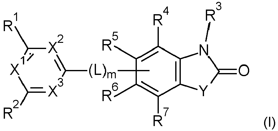 Y represents NR10, CR8R9, O or S, preferably NR10;R10 represents hydrogen, an unsubstituted or substituted aromatic hydrocarbon group containing 6 to 30 ring atoms or an unsubstituted or substituted heteroaromatic group containing 3 to 30 ring atoms, an unsubstituted or substituted alkyl group having 1 to 25 carbon atoms or an unsubstituted or substituted cycloalkyl group having 3 to 18 ring carbon atoms;R8 and R9 each independently represents hydrogen, an unsubstituted or substituted aromatic hydrocarbon group containing 6 to 30 ring atoms or an unsubstituted or substituted heteroaromatic group containing 3 to 30 ring atoms, an unsubstituted or substituted alkyl group having 1 to 25 carbon atoms or an unsubstituted or substituted cycloalkyl group having 3 to 18 ring carbon atoms;
orR8 and R9 form together a substituted or unsubstituted carbocyclic or heterocyclic ring; R1 and R2 each independently represents hydrogen, an unsubstituted or substituted aromatic hydrocarbon group containing 6 to 30 ring atoms or an unsubstituted or substituted heteroaromatic group containing 3 to 30 ring atoms, an unsubstituted or substituted alkyl group having 1 to 25 carbon atoms, an unsubstituted or substituted cycloalkyl group having 3 to 18 ring carbon atoms or CN;R3 represents hydrogen, an unsubstituted or substituted aromatic hydrocarbon group containing 6 to 30 ring atoms or an unsubstituted or substituted heteroaromatic group containing 3 to 30 ring atoms, an unsubstituted or substituted alkyl group having 1 to 25 carbon atoms or an unsubstituted or substituted cycloalkyl group having 3 to 18 ring carbon atoms;R4, R5, R6 and R7 each independently represents hydrogen, an unsubstituted or substituted aromatic hydrocarbon group containing 6 to 30 ring atoms or an unsubstituted or substituted heteroaromatic group containing 3 to 30 ring atoms, an unsubstituted or substituted alkyl group having 1 to 25 carbon atoms, an unsubstituted or substituted cycloalkyl group having 3 to 18 ring carbon atoms or CN; ortwo adjacent groups selected from R4 and R5, R5 and R6 or R6 and R7 form together a substituted or unsubstituted carbocyclic or heterocyclic ring;wherein one of R4, R5, R6 and R7 is a bonding site;X1 represents N or CR11;X2 represents N or CR12;X3 represents N or CR13;wherein at least one, preferably at least two of X1, X2 and X3 are N;R11, R12 and R13 each independently represents hydrogen, an unsubstituted or substituted aromatic hydrocarbon group containing 6 to 30 ring atoms, an unsubstituted or substituted heteroaromatic group containing 3 to 30 ring atoms, an unsubstituted or substituted alkyl group having 1 to 25 carbon atoms or an unsubstituted or substituted cycloalkyl group having 3 to 18 ring carbon atoms;
orR1 and R11 and/or R12; and/or R2 and R-11 and/or R13 may form together a a substituted or unsubstituted carbocyclic or heterocyclic ring;L represents an unsubstituted or substituted divalent aromatic hydrocarbon group containing 6 to 30 ring atoms or an unsubstituted or substituted divalent heteroaromatic group containing 3 to 30 ring atoms;m represents 1, 2, 3 or 4, preferably 1, 2 or 3, wherein the groups L are identical or different in the case that m is > 1. - The compound according to claim 1, wherein Y represents NR10.
- The compound according to claim 1 or 2, wherein R1 and R2 each independently represents hydrogen, an unsubstituted or substituted aromatic hydrocarbon group containing 6 to 30 ring atoms or an unsubstituted or substituted heteroaromatic group containing 3 to 30 ring atoms.
- The compound according to any one of claims 1 to 3, wherein R4, R5, R6 and R7 are hydrogen, wherein one of R4, R5, R6 and R7 is a bonding site.
- The compound according to any one of claims 1 to 4, wherein R3 and R10 each independently represents an unsubstituted or substituted aromatic hydrocarbon group containing 6 to 18 ring atoms, an unsubstituted or substituted heteroaromatic group containing 3 to 18 ring atoms, an unsubstituted or substituted cycloalkyl group having 5 to 8 ring carbon atoms, or an unsubstituted or substituted alkyl group having 1 to 8 carbon atoms.
- The compound according to claim 5, wherein R3 and R10 each independently represents methyl, ethyl, n-propyl, isopropyl, phenyl, naphthyl pyridyl or quinoline.
- The compound according to any one of claims 1 to 6, wherein L represents an unsubstituted or substituted divalent aromatic hydrocarbon group containing 6 to 24 ring atoms, preferably 6 to 18 ring atoms, or an unsubstituted or substituted divalent heteroaromatic group containing 3 to 24 ring atoms, preferably 3 to 18 ring atoms; more preferably, L represents an unsubstituted or substituted divalent phenyl group, an unsubstituted or substituted divalent naphthyl group, an unsubstituted or substituted divalent anthryl group, an unsubstituted or substituted phenanthryl group, an unsubstituted or substituted triphenylenyl group, a 9,9-dimethyl fluorene group, an unsubstituted or substituted 9,9-diphenyl fluorene group, or an unsubstituted or substituted divalent heteroaromatic group containing 3 to 24 ring atoms, preferably 3 to 14 ring atoms; most preferably unsubstituted 1,4-phenylene, unsubstituted 1,3-phenylene, 1,4-phenylene substituted with phenyl, naphthyl or phenanthryl, 1,3-phenylene substituted with phenyl, naphthyl or phenanthryl, unsubstituted 1,4-naphthalene, unsubstituted 1,5-naphthalene, unsubstituted 1,6-naphthalene, unsubstituted 2,6-naphthalene, unsubstituted 2,7-9,9-diphenyl-fluorene, unsubstituted 2,5-9,9-diphenyl-fluorene, unsubstituted 2,7-9,9-dimethyl-fluorene, unsubstituted 2,5-9,9-dimethyl-fluorene, unsubstituted 2,7-triphenylene, unsubstituted 9,10-anthryl, substituted 9,6-anthryl, substituted 9,7-anthryl, or an unsubstituted divalent heteroaromatic group containing 3 to 24 ring atoms, preferably 3 to 14 ring atoms.
- The compound according to any one of claims 1 to 7, wherein the group -(L)m- is represented by:


- A material for an organic electroluminescence device, comprising at least one compound according to any one of claims 1 to 8.
- An organic electroluminescence device comprising at least one compound according to any one of claims 1 to 8, the organic electroluminescence device preferably comprises a cathode, an anode and one or more organic thin film layers comprising an emitting layer disposed between the cathode and the anode, wherein at least one layer of the organic thin film layers comprises at least one compound according to any one of claims 1 to 8.
- The organic electroluminescence device according to claim 10, wherein the organic thin film layers comprise an electron-transporting zone provided between the emitting layer and the cathode, wherein the electron-transporting zone comprises at least one compound according to any one of claims 1 to 8.
- The organic electroluminescence device according to claim 11, wherein the electron-transporting zone comprises an electron-transporting layer provided between the emitting layer and the cathode, wherein the electron-transporting layer comprises at least one compound according to any one of claims 1 to 8.
- The organic electroluminescence device according to claims 11 to 12, wherein the electron-transporting zone further comprises at least one metal, metal complex or metal compound, wherein the at least one metal, metal complex or metal compound is preferably at least one selected from the group consisting of an alkali metal, an alkali metal compound, an alkali metal complex, an alkaline earth metal, an alkaline earth metal compound, an alkaline earth metal complex, a rare earth metal, a rare earth metal compound, and a rare earth metal complex.
- An electronic equipment comprising the organic electroluminescence device according to any one of claims 10 to 13.
- Use of a compound of formula (I) according to any one of claims 1 to 8 in an organic electroluminescence device, wherein the organic electroluminescence device preferably comprises a cathode, an anode and one or more organic thin film layers comprising an emitting layer disposed between the cathode and the anode, wherein the organic thin film layers more preferably comprise an electron-transporting zone provided between the emitting layer and the cathode, wherein most preferably the electron-transporting zone comprises at least one compound according to any one of claims 1 to 8.
Priority Applications (4)
| Application Number | Priority Date | Filing Date | Title |
|---|---|---|---|
| EP21193207.4A EP4140994A1 (en) | 2021-08-26 | 2021-08-26 | Compound, material for an organic electroluminescence device and an organic electroluminescence device comprising the compound |
| KR1020247005512A KR20240052749A (en) | 2021-08-26 | 2022-08-25 | Compounds, materials for organic electroluminescent devices, and organic electroluminescent devices containing the compounds |
| PCT/JP2022/032896 WO2023027196A1 (en) | 2021-08-26 | 2022-08-25 | Compound, material for an organic electroluminescence device and an organic electroluminescence device comprising the compound |
| CN202280054116.6A CN117794915A (en) | 2021-08-26 | 2022-08-25 | Compound, material for organic electroluminescent device comprising the same, and organic electroluminescent device |
Applications Claiming Priority (1)
| Application Number | Priority Date | Filing Date | Title |
|---|---|---|---|
| EP21193207.4A EP4140994A1 (en) | 2021-08-26 | 2021-08-26 | Compound, material for an organic electroluminescence device and an organic electroluminescence device comprising the compound |
Publications (1)
| Publication Number | Publication Date |
|---|---|
| EP4140994A1 true EP4140994A1 (en) | 2023-03-01 |
Family
ID=77518977
Family Applications (1)
| Application Number | Title | Priority Date | Filing Date |
|---|---|---|---|
| EP21193207.4A Withdrawn EP4140994A1 (en) | 2021-08-26 | 2021-08-26 | Compound, material for an organic electroluminescence device and an organic electroluminescence device comprising the compound |
Country Status (4)
| Country | Link |
|---|---|
| EP (1) | EP4140994A1 (en) |
| KR (1) | KR20240052749A (en) |
| CN (1) | CN117794915A (en) |
| WO (1) | WO2023027196A1 (en) |
Citations (8)
| Publication number | Priority date | Publication date | Assignee | Title |
|---|---|---|---|---|
| WO2008105515A1 (en) * | 2007-02-28 | 2008-09-04 | Taisho Pharmaceutical Co., Ltd. | Novel hydroxamic acid derivative |
| WO2010134350A1 (en) | 2009-05-22 | 2010-11-25 | 出光興産株式会社 | Organic electroluminescent element |
| WO2012105629A1 (en) | 2011-02-02 | 2012-08-09 | 出光興産株式会社 | Nitrogenated heterocyclic derivative, electron-transporting material for organic electroluminescent elements, and organic electroluminescent element using same |
| WO2013064206A1 (en) | 2011-11-01 | 2013-05-10 | Merck Patent Gmbh | Organic electroluminescent device |
| WO2016128103A1 (en) | 2015-02-09 | 2016-08-18 | Merck Patent Gmbh | Electronic device containing cyclic lactams |
| CN108727388A (en) * | 2017-04-14 | 2018-11-02 | 北京鼎材科技有限公司 | compound and organic electroluminescence device |
| CN110003116A (en) | 2019-04-23 | 2019-07-12 | 中节能万润股份有限公司 | A kind of organic photoelectrical material and the preparation method and application thereof containing cyclic annular ureas structure |
| DE102020007381A1 (en) * | 2019-12-19 | 2021-06-24 | MERCK Patent Gesellschaft mit beschränkter Haftung | SPIROINDOLENONE |
Family Cites Families (1)
| Publication number | Priority date | Publication date | Assignee | Title |
|---|---|---|---|---|
| KR102303425B1 (en) * | 2019-10-01 | 2021-09-23 | (주)씨엠디엘 | Benzimidazolone derivatives organic light emitting compound and organic electroluminescent device including the same |
-
2021
- 2021-08-26 EP EP21193207.4A patent/EP4140994A1/en not_active Withdrawn
-
2022
- 2022-08-25 KR KR1020247005512A patent/KR20240052749A/en unknown
- 2022-08-25 CN CN202280054116.6A patent/CN117794915A/en active Pending
- 2022-08-25 WO PCT/JP2022/032896 patent/WO2023027196A1/en active Application Filing
Patent Citations (9)
| Publication number | Priority date | Publication date | Assignee | Title |
|---|---|---|---|---|
| WO2008105515A1 (en) * | 2007-02-28 | 2008-09-04 | Taisho Pharmaceutical Co., Ltd. | Novel hydroxamic acid derivative |
| WO2010134350A1 (en) | 2009-05-22 | 2010-11-25 | 出光興産株式会社 | Organic electroluminescent element |
| WO2012105629A1 (en) | 2011-02-02 | 2012-08-09 | 出光興産株式会社 | Nitrogenated heterocyclic derivative, electron-transporting material for organic electroluminescent elements, and organic electroluminescent element using same |
| EP2672540A1 (en) * | 2011-02-02 | 2013-12-11 | Idemitsu Kosan Co., Ltd. | Nitrogenated heterocyclic derivative, electron-transporting material for organic electroluminescent elements, and organic electroluminescent element using same |
| WO2013064206A1 (en) | 2011-11-01 | 2013-05-10 | Merck Patent Gmbh | Organic electroluminescent device |
| WO2016128103A1 (en) | 2015-02-09 | 2016-08-18 | Merck Patent Gmbh | Electronic device containing cyclic lactams |
| CN108727388A (en) * | 2017-04-14 | 2018-11-02 | 北京鼎材科技有限公司 | compound and organic electroluminescence device |
| CN110003116A (en) | 2019-04-23 | 2019-07-12 | 中节能万润股份有限公司 | A kind of organic photoelectrical material and the preparation method and application thereof containing cyclic annular ureas structure |
| DE102020007381A1 (en) * | 2019-12-19 | 2021-06-24 | MERCK Patent Gesellschaft mit beschränkter Haftung | SPIROINDOLENONE |
Non-Patent Citations (5)
| Title |
|---|
| ANGEW. CHEM., vol. 114, 2002, pages 4218 - 4221 |
| CHEMICAL REVIEWS, vol. 95, 1995, pages 2457 - 2483 |
| JOURNAL OF AMERICAN CHEMISTRY SOCIETY, vol. 121, 1999, pages 9550 - 9561 |
| KUMADA, ORG. LETT., vol. 12, 2010, pages 2298 - 2301 |
| YOU-GUI LI ET AL: "Bulky Phosphane Ligand for Monoselective Ruthenium-Catalyzed, Directed o-CH Arylation with Challenging Aryl Chlorides", SYNLETT, vol. 28, no. 04, 9 November 2016 (2016-11-09), DE, pages 499 - 503, XP055582242, ISSN: 0936-5214, DOI: 10.1055/s-0036-1588635 * |
Also Published As
| Publication number | Publication date |
|---|---|
| CN117794915A (en) | 2024-03-29 |
| KR20240052749A (en) | 2024-04-23 |
| WO2023027196A1 (en) | 2023-03-02 |
Similar Documents
| Publication | Publication Date | Title |
|---|---|---|
| JP6434073B2 (en) | Organic electroluminescence device | |
| EP2790239B1 (en) | Material for organic electroluminescent element and organic electroluminescent element | |
| KR102261235B1 (en) | Aromatic heterocyclic derivative, material for organic electroluminescent element, and organic electroluminescent element | |
| KR20140094520A (en) | Organic electroluminescence element, and material for organic electroluminescence element | |
| KR20140092332A (en) | Organic electroluminescence element and material for organic electroluminescence element | |
| KR20150030660A (en) | Biscarbazole derivative host materials and red emitter for oled emissive region | |
| US11289661B2 (en) | Nitrogen-containing heterocyclic compounds for organic light emitting devices | |
| WO2018116152A1 (en) | Specifically substituted ladder type compounds for organic light emitting devices | |
| WO2014021280A1 (en) | Organic electroluminescent element | |
| EP4140994A1 (en) | Compound, material for an organic electroluminescence device and an organic electroluminescence device comprising the compound | |
| US20220109115A1 (en) | Polycyclic compound, and an organic electroluminescence device comprising the polycyclic compound | |
| EP4124619A1 (en) | Compound, material for an organic electroluminescence device and an organic electroluminescence device comprising the compound | |
| EP4043453A1 (en) | Compound, material for an organic electroluminescence device and an organic electroluminescence device comprising the compound | |
| EP4060756A1 (en) | An organic electroluminescence device comprising an azine compound and a rare earth metal, rare earth metal compound, and/or rare earth metal complex and an electronic equipment comprising said organic electroluminescence device | |
| EP3882238A1 (en) | Compound, material for an organic electroluminescence device and an organic electroluminescence device comprising the compound | |
| US20230123170A1 (en) | Compound, material for an organic electroluminescence device and an organic electroluminescence device comprising the compound | |
| EP4349934A1 (en) | A highly efficient blue fluorescent organic emitter having a high homo level and an organic electroluminescence device comprising the same | |
| EP4215535A1 (en) | Compound and an organic electroluminescence device comprising the compound | |
| EP3865486A1 (en) | Heterocyclic compound and an organic electroluminescence device comprising the heterocyclic compound | |
| EP4068404A1 (en) | An organic electroluminescence device comprising a light emitting layer comprising three different compounds and an electronic equipment comprising said organic electroluminescence device | |
| EP4151697A1 (en) | Compound and an organic electroluminescence device comprising the compound | |
| US20230099759A1 (en) | Polycyclic compound, material for an organic electroluminescence device and an organic electroluminescence device comprising the polycyclic compound | |
| US11616201B2 (en) | Specific ladder type compounds for organic light emitting devices | |
| US20230416278A1 (en) | Heterocyclic compound and an organic electroluminescence device comprising the heterocyclic compound | |
| EP3604477A1 (en) | Polycyclic compound, organic electroluminescence device, and electronic device |
Legal Events
| Date | Code | Title | Description |
|---|---|---|---|
| PUAI | Public reference made under article 153(3) epc to a published international application that has entered the european phase |
Free format text: ORIGINAL CODE: 0009012 |
|
| STAA | Information on the status of an ep patent application or granted ep patent |
Free format text: STATUS: THE APPLICATION HAS BEEN PUBLISHED |
|
| AK | Designated contracting states |
Kind code of ref document: A1 Designated state(s): AL AT BE BG CH CY CZ DE DK EE ES FI FR GB GR HR HU IE IS IT LI LT LU LV MC MK MT NL NO PL PT RO RS SE SI SK SM TR |
|
| STAA | Information on the status of an ep patent application or granted ep patent |
Free format text: STATUS: THE APPLICATION IS DEEMED TO BE WITHDRAWN |
|
| 18D | Application deemed to be withdrawn |
Effective date: 20230902 |