Technical Field
-
Embodiments of the present disclosure relate to the failure analysis of processing systems, such as micro-controllers.
Background
-
Figure 1 shows a typical electronic system, such as the electronic system of a vehicle, comprising a plurality of processing systems 10, such as embedded systems or integrated circuits, e.g., a Field Programmable Gate Array (FPGA), a Digital Signal Processor (DSP) or a micro-controller (e.g., dedicated to the automotive market).
-
For example, in Figure 1 are shown three processing systems 101, 102 and 103 connected through a suitable communication system 20. For example, the communication system may include a vehicle control bus, such as a Controller Area Network (CAN) bus, and possibly a multimedia bus, such as a Media Oriented Systems Transport (MOST) bus, connected to vehicle control bus via a gateway. Typically, the processing systems 10 are located at different positions of the vehicle and may include, e.g., an Engine Control Unit, a Transmission Control Unit (TCU), an Anti-lock Braking System (ABS), a Body Control Module (BCM), and/or a navigation and/or multimedia audio system. Accordingly, one or more of the processing systems 10 may also implement real-time control and regulation functions. These processing systems are usually identified as Electronic Control Units.
-
Figure 2 shows a block diagram of an exemplary digital processing system 10, such as a micro-controller, which may be used as any of the processing systems 10 of Figure 1.
-
In the example considered, the processing system 10 comprises a microprocessor 102, usually the Central Processing Unit (CPU), programmed via software instructions. Usually, the software executed by the microprocessor 102 is stored in a non-volatile program memory 104, such as a Flash memory or EEPROM. Thus, the memory 104 is configured to store the firmware of the processing unit 102, wherein the firmware includes the software instructions to be executed by the microprocessor 102. Generally, the non-volatile memory 104 may also be used to store other data, such as configuration data, e.g., calibration data.
-
The microprocessor 102 usually has associated also a volatile memory 104b, such as a Random-Access-Memory (RAM). For example, the memory 104b may be used to store temporary data.
-
As shown in Figure 2, usually the communication with the memories 104 and/or 104b is performed via one or more memory controllers 100. The memory controller(s) 100 may be integrated in the microprocessor 102 or connected to the microprocessor 102 via a communication channel, such as a system bus of the processing system 10. Similarly, the memories 104 and/or 104b may be integrated with the microprocessor 102 in a single integrated circuit, or the memories 104 and/or 104b may be in the form of a separate integrated circuit and connected to the microprocessor 102, e.g., via the traces of a printed circuit board.
-
In the example considered, the microprocessor 102 may have associated one or more (hardware) resources/peripherals 106 selected from the group of:
- one or more communication interfaces IF, e.g., for exchanging data via the communication system 20, such as a Universal asynchronous receiver/transmitter (UART), Serial Peripheral Interface Bus (SPI), Inter-Integrated Circuit (I2C), Controller Area Network (CAN) bus, and/or Ethernet interface, and/or a debug interface; and/or
- one or more analog-to-digital converters AD and/or digital-to-analog converters DA; and/or
- one or more dedicated digital components DC, such as hardware timers and/or counters, or a cryptographic co-processor; and/or
- one or more analog components AC, such as comparators, sensors, such as a temperature sensor, etc.; and/or
- one or more mixed signal components MSC, such as a PWM (Pulse-Width Modulation) driver.
-
Generally, a dedicated digital components DC may also correspond to a FPGA integrated in the processing system 10. For example, in this case, the memory 104 may also comprise the program data for such a FPGA.
-
Accordingly, the digital processing system 10 may support different functionalities. For example, the behavior of the microprocessor 102 is determined by the firmware stored in the memory 104, e.g., the software instructions to be executed by a microprocessor 102 of a micro-controller 10. Thus, by installing a different firmware, the same hardware (micro-controller) can be used for different applications.
-
In this respect, future generation of such processing systems 10, e.g., micro-controllers adapted to be used in automotive applications, are expected to exhibit an increase in complexity, mainly due to the increasing number of requested functionalities (new protocols, new features, etc.) and to the tight constraints of execution conditions (e.g., lower power consumption, increased calculation power and speed, etc.).
-
For example, recently more complex multi-core processing systems 10 have been proposed. For example, such multi-core processing systems may be used to execute (in parallel) several of the processing systems 10 shown in Figure 1, such as several processing systems of a vehicle.
-
Figure 3 shows an example of a multi-core processing system 10. Specifically, in the example considered, the processing system 10 comprises a plurality of n processing cores 1021...102n connected to a (on-chip) communication system 114. For example, in the context of real-time control systems, the processing cores 1021...102n may be ARM Cortex®-R52 cores. Generally, the communication system 114 may comprise one or more bus systems, e.g., based on the Advanced eXtensible Interface (AXI) bus architecture, and/or a Network-on-Chip (NoC).
-
For example, as shown at the example of the processing core 1021, each processing core 102 may comprise a microprocessor 1020 and a communication interface 1022 configured to manage the communication between the microprocessor 1020 and the communication system 114. Typically, the interface 1022 is a master interface configured to forward a given (read or write) request from the microprocessor 1020 to the communication system 114, and forward an optional response from the communication system 114 to the microprocessor 1020. However, the communication interface 1022 may also comprise a slave interface. For example, in this way, a first microprocessor 1020 may send a request to a second microprocessor 1020 (via the communication interface 1022 of the first microprocessor, the communication system 114 and the communication interface 1022 of the second microprocessor).
-
Generally, each processing core 1021...102n may also comprise further local resources, such as one or more local memories 1026, usually identified as Tightly Coupled Memory (TCM).
-
As mentioned before, typically the processing cores 1021...102n are arranged to exchange data with a non-volatile memory 104 and/or a volatile memory 104b. In a multi-core processing system 10, often these memories are system memories, i.e., shared for the processing cores 1021...102n. As mentioned before, each processing cores 1021...102n may, however, comprise one or more additional local memories 1026.
-
For example, as shown in Figure 3, the processing system 10 may comprise one or more memory controllers 100 configured to connect at least one non-volatile memory 104 and at least one volatile memory 104b to the communication system 114. As mentioned before, one or more of the memories 104 and/or 104b may be integrated in the integrated circuit of the processing system 10 or connected externally to the integrated circuit. For example, the processing system 10 may comprise:
- a first volatile memory 104b integrated in the integrated circuit of the processing system 10 and connected to the communication system 114 via a first memory controller 100, and
- a second volatile memory 104b external with respect to the integrated circuit of the processing system 10 and connected to the communication system 114 via a second memory controller 100.
-
As mentioned before, the processing system 10 may comprise one or more resources 106, such as one or more communication interfaces or co-processors (e.g., a cryptographic co-processor). The resources 106 are usually connected to the communication system 114 via a respective communication interface 1062. In general, the communication interface 1062 comprises at least a slave interface. For example, in this way, a processing core 102 may send a request to a resource 106 and the resource returns given data. Generally, one or more of the communication interfaces 1062 may also comprise a respective master interface. For example, such a master interface 1064 may be useful in case the resource has to start a communication in order to exchange data via (read and/or write) request with another circuit connected to the communication system 114, such as a resource 106 or a processing core 102. For example, for this purpose, the communication system 114 may indeed comprise an Advanced Microcontroller Bus Architecture (AMBA) High-performance Bus (AHB), and an Advanced Peripheral Bus (APB) used to connect the resources/peripherals 106 to the AMBA AHB bus.
-
Often such processing systems 10 comprise also one or more Direct Memory Access (DMA) controllers 110. For example, as shown in Figure 3, a DMA controller 110 may be used to directly exchange data with a memory, e.g., the memory 104b, based on requests received from a resource 106. For example, in this way, a communication interface IF may directly read data (via the DMA controller 110) from the memory 104b and transmit these data, without having to exchange further data with a processing unit 102. Generally, a DMA controller 110 may communicate with the memory or memories via the communication system 114 or via one or more dedicated communication channels.
-
In this respect, irrespective of the complexity of the processing system 10 (e.g., with respect to the number of processing cores 102 and/or number and type of the resources 106), a typical product development involves several entities, such as the producer of the integrated circuit comprising the processing system 10, one or more hardware developers, which implement a more complex electronic circuit and one or more software developers, which write the firmware for the processing system 10.
-
On the one hand, this implies that the validation of the various hardware and/or software functionalities of each processing system 10 during the respective development stage may involve a significant portion of the overall development costs: this applies both at the company producing the processing system 10 and the customer side, where the application is developed.
-
On the other hand, also the hardware modules within the processing systems 10 implementing security functions are getting more and more important. For example, this may apply to a debug interface, and/or access to given memory locations in the non-volatile memory 104 and/or volatile memory 104b. For example, various processing systems 10 provide the possibility to configure whether the access to the internal resource of the processing system 10 via a debug interface is blocked or permitted (possibly specifying whether data may only be read or also written). For example, usually during the development stage it should be possible to control the resources of the processing system 10 with a given degree of freedom, while the processing system 10 should be configured to activate certain security functions (which may not be altered) when the processing system 10 is "in field" (i.e., running in the final application).
-
For example, most modern micro-controllers use solutions where the enabling of a security feature is done by programming the on/off status in a non-volatile memory. These configuration data are then read during the reset phase in order to enable or disable the related protections, e.g., in order to disable the debug interface of the micro-controller. Thus, a relevant portion of the security configuration is not alterable anymore after the respective configuration information have been programmed into the non-volatile memory, e.g., because, once the debug interface has been deactivated, it is also impossible to overwrite the configuration data. Accordingly, most of the security configuration, once enforced, are not alterable and the protection is always active. Unfortunately, in this way it is also difficult to analyses possible malfunctions of the processing system 10 occurring only in field.
-
Accordingly, as also described in European Patent Application n.
EP 3 413 194 A1 , which is incorporated herein by reference, various modern processing systems permit to activate the security functions of the
processing systems 10 based on so called life-cycle data LCD.
-
For example, as disclosed in
EP 3 413 194 A1 , the bit sequence LCD may indicate one of the following stages:
- "production" (LC1), when the processing system 10, e.g., a micro-controller, is in the chip fabric;
- "customer delivery" (LC2), when the processing system 10 has been shipped to the 1st tier customer (e.g., a producer of an engine control unit);
- "OEM production" (LC3), when the device has been shipped to a next-level customer (e.g., a car maker); and
- "in field" (LC4), when the device is installed in the final product (e.g., in a car sold in the market).
-
Typically, the life-cycle data LCD are written such that once a certain stage is reached, it is not possible to revert it back to a previous stage, i.e., the life-cycle can only advance. Accordingly, the life-cycle data LCD are a permanent signature written into a non-volatile memory, which determines the stage of the processing system 10 during its life-time. For example, each life-cycle may be encoded with a respective bit sequence. For example, as shown in Figure 3, this bit sequence LCD may be stored to a one-time programmable memory 126. For example, this may be implemented with a one-hot encoding in which a fuse is burned each time a given stage has been reached. In general, the life-cycle data LCD may also be stored at reserved memory locations of the non-volatile memory 104.
-
Accordingly, the advancing of the life-cycle to the next stage may be done by the entity who owns the device in the current life-cycle stage (e.g., chip producer will advance the life-cycle when it is shipped to the customer delivery stage; the 1st tier customer will advance the life-cycle when it is shipped to the OEM production stage, etc.).
-
As mentioned before, typically an increasing number of security features of the processing system 10 are activated when advancing the life-cycle stage. Generally, such security features target the protection of several micro resources, so that the access to them is blocked. For example, the life-cycle data LCD may be provided to:
- a resource 106, such as a debug interface, which is enabled or disabled as a function of the data LCD; and/or
- a memory 104 and/or 104b which inhibits (read and/or write) access to given memory address ranges; and/or
- a processing core 102, which may execute a firmware which changes operation based on the data LCD, thereby implementing a software-based protection mechanism.
-
This operation blocks thus possible unauthorized accesses, e.g., by a hacker, but also limits the possibility to test/analyze the device, and the most critical scenario is when a device returns due to a malfunction. In fact, in order to be able to analyze the failure root cause, several security layers, which could be put in place by the 1st Tier and OEM customers, need to be bypassed. This operation can be difficult for a hard-failing unit, therefore a stage, called Failure Analysis, is usually adopted, which automatically removes some non-security critical protections, making it possible to run failure analysis tests, i.e., the life-cycle data LCD may indicate the following further stage:
- "failure analysis" (LC5), when the device is shipped back (e.g., to the producer of the processing system 10 or the hardware or software developer) for diagnostic purposes.
-
Thus, the failure analysis stage represents a special situation, because the failure analysis stage may be reached by advancing the live cycle stage, but one or more of the previously activated security mechanisms are now disable, e.g., the debug interface is again enabled. In this respect, modern processing systems 10 may enable, once the device reaches the failure analysis stage, other protection mechanisms, like a permanent impossibility to re-use the device in a car after the failure analysis stage is started.
-
Accordingly, in order to avoid possible attacks and from a safety point of view, the entrance in the failure analysis stage has to be a well-controlled operation and should never happen accidentally. For example, activating accidentally the failure analysis stage in a real-time electronic control system could have catastrophic consequences when the device is still active in the field.
Summary
-
In view of the above, it is an objective of various embodiments of the present disclosure to provide solutions for programming the life-cycle stage of a processing system.
-
According to one or more embodiments, one or more of the above objectives is achieved by means of a processing system having the features specifically set forth in the claims that follow. Embodiments moreover concern a related integrated circuit, device and method.
-
The claims are an integral part of the technical teaching of the disclosure provided herein.
-
As mentioned before, various embodiments of the present disclosure relate to a processing system, e.g., implemented in an integrated circuit.
-
In various embodiments, the processing system comprises a digital processing core comprising a microprocessor configured to execute software instruction. The processing system comprises also a hardware circuit, e.g., a peripheral of the processing system, configured to change operation as a function of decoded life-cycle data indicating a life-cycle stage. Specifically, a non-volatile memory is configured to stored encoded life-cycle data indicating a life-cycle stage. Accordingly, the processing system comprises also a hardware configuration circuit configured to read the encoded life-cycle data from the non-volatile memory, generate the decoded life-cycle data by decoding the encoded life-cycle data, and provide the decoded life-cycle data to the hardware circuit.
-
In various embodiments, the processing system comprises a reset terminal, e.g., a pad or pin of a respective integrated circuit, configured to receive an external reset signal, and a reset circuit configured to monitor the external reset signal received via the reset terminal. In various embodiments, the reset circuit is configured, in response to determining that the external reset signal has a first logic level, to execute a sequence of operations. Specifically, during a reset phase, the reset circuit generates a reset of the processing system. During a configuration phase, the reset circuit activates the hardware configuration circuit, whereby the hardware configuration circuit reads the encoded life-cycle data, decodes the encoded life-cycle data and provides the decoded life-cycle data to the hardware circuit. During a wait phase, the reset circuit waits until the external reset signal has a second logic level. Conversely, in response to determining that the external reset signal has the second logic level, the reset circuit starts the microprocessor, i.e., the microprocessor starts to execute software instructions.
-
In various embodiments, the processing system comprises a communication interface activated during the wait phase and configured to receive a request from an external device. For example, the communication interface may be a serial communication interface, preferably a JTAG interface.
-
In various embodiments, the processing system comprises a hardware verification circuit. Specifically, this verification circuit is configured to verify (at least) whether the request comprises a given reference password and whether the reset circuit is in the wait phase. In various embodiments, in response to determining that the request comprises a given reference password and the reset circuit is in the wait phase, the verification circuit generates a life-cycle advancement request signal indicating a request to advance the life-cycle stage indicated by the encoded life cycle data to a given predetermined life-cycle stage.
-
Generally, the verification circuit may also verify further conditions. For example, in various embodiments, the processing system comprises a test-mode terminal configured to receive an external test-mode signal. In this case, the verification circuit may be configured to verify whether the external test-mode signal has a given logic level, and generate the life-cycle advancement request signal only when the external test-mode signal has the given logic level.
-
Additionally or alternatively, the verification circuit may use an enable flag. For example, in various embodiments, the processing system comprises a plurality of configuration data clients, each configuration data client comprising a register for storing configuration data. In this case, the non-volatile memory may be configured to stored also configuration data, and the hardware configuration circuit may be configured, during the configuration phase, to read the configuration data from the non-volatile memory and transmit the configuration data to the plurality of configuration data clients. Accordingly, in this case, the verification circuit may be configured to receive the enable flag from a configuration data client, verify whether the enable flag has a given logic level and generate the life-cycle advancement request signal only when the enable flag has the given logic level.
-
In various embodiments, the verification circuit may be configured to receive similarly the reference password from a configuration data client.
-
Accordingly, in various embodiments, a write circuit of the non-volatile memory may be configured to monitor the life-cycle advancement request signal and, in response to determining that the life-cycle advancement request signal is set, write one or more bits of the encoded life-cycle data stored in the non-volatile memory, thereby advancing the life-cycle stage indicated by the encoded life cycle data to the given predetermined life-cycle stage.
-
In various embodiments, the processing system comprises at least three registers, wherein the life-cycle advancement request signal is stored to this at least three registers. In this case, the write circuit may be implemented with a state-machine, such as a hardware state-machine or a further microprocessor, wherein the state machine is configured to read the content of the at least three registers, determine the logic level of the majority of bits of the at least three registers and, in response to determining that the majority of bits are set, write the one or more bits of the encoded life-cycle data stored in the non-volatile memory.
-
For example, in case the state-machine is implemented with (or comprises) a further microprocessor, the at least three registers may be implemented with a register interface of the further microprocessor. Accordingly, in this case, the further microprocessor may be configured to read the content of the at least three registers and determine the logic level of the majority of bits of the at least three registers via software instructions executed by the further microprocessor.
Brief description of the figures
-
Embodiments of the present disclosure will now be described with reference to the annexed drawings, which are provided purely by way of non-limiting example and in which:
- Figure 1 shows an example of an electronic system comprising a plurality of processing systems;
- Figures 2 and 3 show examples of processing systems;
- Figure 4 shows an embodiment of a processing system according to the present disclosure;
- Figures 5 and 6 show embodiments for distributing configuration data and life-cycle data in the processing system of Figure 4;
- Figure 7 is a flow-chart showing an embodiment of the operation of the processing system of Figure 6;
- Figure 8 shows a further embodiment of a processing system according to the present disclosure; and
- Figures 9, 10, 11, 12 and 13 show embodiments of details of the processing system of Figure 8.
Detailed Description
-
In the following description, numerous specific details are given to provide a thorough understanding of embodiments. The embodiments can be practiced without one or several specific details, or with other methods, components, materials, etc. In other instances, well-known structures, materials, or operations are not shown or described in detail to avoid obscuring aspects of the embodiments.
-
Reference throughout this specification to "one embodiment" or "an embodiment" means that a particular feature, structure, or characteristic described in connection with the embodiment is included in at least one embodiment. Thus, the appearances of the phrases "in one embodiment" or "in an embodiment" in various places throughout this specification are not necessarily all referring to the same embodiment. Furthermore, the particular features, structures, or characteristics may be combined in any suitable manner in one or more embodiments.
-
The headings provided herein are for convenience only and do not interpret the scope or meaning of the embodiments.
-
In the following Figures 4 to 13 parts, elements or components which have already been described with reference to Figures 1 to 3 are denoted by the same references previously used in such Figure; the description of such previously described elements will not be repeated in the following in order not to overburden the present detailed description.
-
As described in the foregoing, modern processing systems may use life-cycle data LCD in order to activate given security protection mechanisms, i.e., the hardware and/or software behavior of the processing system may change as a function of life-cycle data LCD.
-
Usually, the security features are not activated exclusively based of the life-cycle data LCD, but additional security configuration data SCD are used to specify whether a given security feature should be activated, e.g., once a given life-cycle stage has been reached. Typically, these security configuration data SCD are stored together with other configuration data CD to a non-volatile memory 104, e.g., reserved memory locations of the non-volatile memory 104 configured to store the firmware of the processing unit(s) 102. These configuration data CD are typically read during a reset phase of the processing system by some circuit and distributed to the various components (e.g., the processing core(s) 102, the memory controller(s) 100, and/or the resources 106), whereby the security configuration data SCD are provided to the security framework and the security configuration data SCD are used to enable or disable the related protections also as a function of the life-cycle data LCD.
-
In this respect, as disclosed in
document EP 3 413 194 A1 , at least part of the configuration data CD, in particular the security configuration data SCD, may not be alterable anymore after being stored to the non-volatile memory. The reason is to guarantee that a certain security configuration is enforced and not alterable, so that the protection is always active.
-
For example, a conventional solution in order to permit a debugging/testing of the processing system involves that:
- the debug-interface of the processing system is disabled; and
- access to one or more components is possible thorough the processing core 102.
-
Accordingly, in this way, the processing core 102 may receive commands via a communication interface IF of the processing system, such as a CAN interface, and execute given (software) operations as a function of the command received, e.g., read data from a given memory address or write data to a given memory address, wherein the memory addresses are associated, e.g., with given memory locations in the memory 104 and/or 104b, and/or resources 106.
-
For example, the processing core 102 may even be configured to overwrite given security configuration data SCD, thereby disabling given security mechanisms, e.g., enabling again the debug interface.
-
Accordingly, the processing core 102 may implements a software debug interface (essentially a back-door), which may verify further conditions, e.g., verify whether the command comprises a correct password, which are usually not implemented in a hardware debug interface.
-
This means that, once a certain security protection is enabled, it might be necessary "to do something" (e.g., to provide a proper password) as a pre-condition to be able to run a predetermine test routine or debug the processing system. Such a password verification operation may however involve various operations. For example, the password has to be provided to the processing core 102 via a communication interface IF, the password has to be verified and eventually the result of the request has to be transmitted again via communication interface IF. In addition, the password verification operation may also involve encrypted password, wherein the processing core 102 has to forward the encrypted communication or only the encrypted password to a hardware secure module/cryptographic coprocessor of the processing system in order to obtain the plain-text password used for the verification operations. This means that, in some cases, some (hardware and/or software) cryptographic operations may be executed before the password can be used to bypass a certain security protection.
-
Thus, while such a software debug interface may be useful to monitor the operation of the processing system, when the processing system is normally used ("in field" stage), in case of a device failure, it may be more suitable to advance the life-cycle stage of the processing system to the failure-analysis stage (if supported), whereby the processing system itself deactivates given hardware security protections, e.g., automatically reactivates the debug interface of the processing system.
-
However, due to the fact that the debug interface is usually disabled in the "in field" stage, also the advancing of the life-cycle stage may only be performed via the processing core 102. Therefore, in order to advance the device to the Failure Analysis stage, it is necessary to execute some software via a processing core 102. For example, also in this case, the processing core 102 may receive a command via a communication interface, verify a password (possibly including a cryptographic operation), and perform the operations in order to advance the life-cycle stage.
-
Accordingly, the use of a microprocessor 102 as debug interface or for advancing the life-cycle stage may be unsuitable, because a significant number of resources may be involved, such as a processing core 102, the non-volaille memory 104 having stored the software executed by the processing core 102, the volatile memory 104b for storing temporary results of the processing core 102, a communication interface IF and possible other resources 106 (such as a cryptographic co-processor). In fact, usually the failure-analysis stage should be started in case a processing system has a hardware failure. Accordingly, such a software approach may not be suitable, because essentially all main components of the processing system are involved, and the failure of one of these components may inhibit that the processing core 102 may perform software debug operations or advance the life-cycle stage of the processing system.
-
Accordingly, in the following will be described solutions which permit to manage in a more efficient manner the life cycle of a processing system.
-
Figure 4 shows an embodiment of a processing system 10a according to the present description.
-
In the embodiment considered, the underlying architecture of the processing system 10a corresponds to the processing system described with respect to Figures 2 and 3, and the respective description applies in their entirety. Thus, also in this case, the processing system 10a, such as an integrated circuit, comprises:
- at least one processing core 102;
- a memory controller 100 configured to be connected to a (internal or external) non-volatile memory 104;
- at least one resource 106; and
- a communication system 114 connecting the processing core(s) 102, the memory controller 100 and the resource(s) 106.
-
As mentioned before, the behavior of the processing system 10a may also be varied based on configuration data CD and life-cycle data LCD.
-
For example, in line with the description of
EP 3 413 194 A1 , these configuration data CD and life-cycle data LCD may be written into specific areas of the
non-volatile memory 104 and retrieved when the
processing system 10a is powered on. Preferably, the
non-volatile memory 104 is integrated in the integrated circuit and may also be used to store the firmware of the processing core(s) 102. However, the firmware may also be stored in a separate
non-volatile memory 104. For example, the non-volatile program memory may be used, in case the program memory is integrated in the integrated circuit. Conversely, an additional (small) internal
non-volatile memory 104 may be used in case the program memory is an external memory. Accordingly, in various embodiments, the configuration data CD and the life-cycle data LCD are stored in a non-volatile memory of the integrated circuit comprising the blocks requiring configuration data, such as the
processing unit 102 and/or one or more of the
hardware resources 106.
-
For example, the configuration data CD may comprise calibration data used to guarantee that the hardware behavior is uniform, thereby compensating possible production process tolerances. For example, this applies often to the calibration of analog components of the processing system, such as a temperature sensor, analog-to-digital converter, voltage reference, etc. For example, a voltage monitor threshold level of an analog comparator could be "trimmed" to the exact intended value by adjusting some levels with configuration/calibration data, which are written by the producer of the hardware of the processing systems, e.g., the micro-controller producer.
-
Moreover, the configuration data CD may also be used to customize the behavior of the hardware, e.g., the hardware resources 106, according to different application needs. For example, once the firmware of the processing system has been stored in the processing system 10a, some configuration data CD, i.e., the security configuration data SCD, may be written in order to deactivate the debug interface, which e.g., could be used to download the firmware of the processing system 10a. Alternatively, only the access to the non-volatile memory via the debug interface may be disabled, i.e., the debug interface as a whole may not be disabled, but the access of the debug interface to the other circuits may be limited.
-
Thus, generally a first part of the configuration data CD may be written by the producer of the hardware of the processing system (e.g., the producer of an integrated circuit), and/or a second part of the configuration data CD may be written by the developer of the firmware of the processing system 10a.
-
As mentioned before, the programmed configuration data CD may be read during a reset phase, which usually starts as soon as the processing system 10a is powered on.
-
Specifically, as shown in Figure 4, the processing system 10a may comprise for this purpose a hardware configuration circuit 108 configured to read the configuration data CD and the life-cycle data LCD from the non-volatile memory 104 and distribute these data within the processing system 10a.
-
In various embodiments, the hardware configuration module 108 may be configured to read the configuration data CD and the life-cycle data LCD from the non-volatile memory 104 by sending read requests to the memory controller 100 via the communication system 114. Additionally or alternatively, the hardware configuration module 108 may also be connected directly to the memory controller 100 or be configured to read directly the data from the memory 104.
-
Similarly, the hardware configuration module 108 may be configured to send the configuration data CD and the life-cycle data LCD to the various circuits by sending write requests via the communication system 114. However, the hardware configuration module 108 may also use a separate communication channel for the configuration data CD and/or the life-cycle data LCD.
-
For example, Figure 5 shows a possible embodiment of the configuration circuit 108. For example, in the embodiment considered, the configuration data CD are stored in reserved memory areas, e.g., in the form of a plurality of consecutive memory locations.
-
Accordingly, in the embodiment considered, the configuration module 108 accesses the reserved memory areas containing the configuration data CD, reads the configuration data CD and transmits the configuration data CD to a respective block 110 within the processing system 10a. Generally, the block 110 may correspond to any block of the processing system 10a requiring configuration data and may correspond to the processing unit 102, a hardware resource 106, or even a memory 104 and/or 104b. For example, the block 110 may be a debug interface of the processing system 10a, which is enabled or disabled based on the configuration data CD. Similarly, the configuration data CD may be used to configure read and/or write protected areas of a memory.
-
For example, in order to distribute the configuration data CD, each block 110 may have associated a respective configuration data client 112. For example, in Figure 5 are shown three blocks 110a, 110b and 110c and three configuration data clients 112a, 112b and 112c. Generally, each configuration data client 112 may be associated univocally to a single hardware block 110, and provided configuration data only to the associated hardware block 110, e.g., a specific hardware resource 106, or may be associated with a plurality of hardware blocks 110, e.g., a plurality of hardware resource 106. In general, the configuration data clients 112a, 112b and 112c may also be integrated in the respective block 110a, 110b and 110c.
-
Accordingly, in the embodiment considered, the configuration module 108 may determine for each target block 110 to be configured the respective configuration data (selected from the configuration data CD) and transmit the configuration data associated with the target block 110 to the configuration data client 112 associated with the target block 110. Similarly, while reading the configuration data CD from the memory 104, the configuration module 108 may determine the target block(s) for the current configuration information and send the current configuration data to the configuration data client(s) associated with the respective target block(s). Generally, any communication may be used for transmitting the configuration data to the configuration data client 112, including both serial and parallel communications. For example, the configuration module 108 and the configuration data clients 112 may be connected via the communication system 114 or an additional bus, and each configuration data clients 112 may have associated a respective target address.
-
Accordingly, each configuration data client 112 is configured to receive the configuration data from the module 108, store them into the internal register, e.g., store them into one or more internal flip-flops or latches. The data stored in the register may then be used to generate one or more signals, which influence the behavior of one or more hardware blocks 110.
-
Figure 6 shows in this respect a possible embodiment of the communication between the configuration module 108 and the configuration data clients 112.
-
Specifically, also in this case, the processing system 10a comprises a configuration module 108 configured to read the configuration data CD from one or more non-volatile memories 104 and a plurality of configuration data clients 112 configured to receive respective configuration data from the module 108 and distribute them among a plurality of blocks 110 (not shown) requiring configuration data. For example, as mentioned before, each configuration data client 112 may be associate univocally with a respective circuit 110. For example, in the embodiment considered, the processing system 10a comprises again three configuration data clients 112a, 112b and 112c.
-
In the embodiment considered, the configuration module 108 comprises a data read module 1080 configured to read the configuration data CD from the memory 104 and a dispatch module 1082 configured to transmit the configuration data to the configuration data clients 112.
-
As mentioned before, any communication may be used for the communication between the dispatch module 1082 and the configuration data clients 112. For example, in various embodiments, the communication between the dispatch module 1082 and the configuration data clients 112 is based on data frames in accordance with a given format, called in the following Device Configuration Format (DCF). For example, in various embodiments, each data frame comprises two fields: the payload (i.e., the real data), called DCF Format payload, and possible additional data attributes used to identify the receiver of the data, called DCF Format attributes, wherein the receiver is one of the configuration data clients 112 representing a DCF client. For example, the data attributes may consist in 16 or 32 bits, wherein a given number of bits specifies the address of one of the configuration data clients 112, and the payload may consist in 16 or 32 bits. For example, in various embodiments, the data read module 1080 is configured to read blocks of 64 bits from the memory 104, wherein the first 32 bits contain the data attributes (including the address of a configuration data client) and the second 32 bits contain the configuration data to be transmitted to the address specified in the data attributes. As mentioned before, the address may correspond to a physical address of the communication system 114 or of a separate communication bus.
-
As described before, each configuration data client/DCF client 112 may be a hardware module, usually comprising a combinational circuit configured to store the received data in an internal register implemented, e.g., with flip-flops/latches, thereby permitting to distribute, via one or more internal signals generated as a function of the data stored in the internal register, the configuration data received to various parts of the associate hardware circuit(s) 110. For example, as mentioned before, each configuration data client 112 may have associated a univocal address (i.e., univocal within each processing system 10a) and analyses the data transmitted by the dispatch module 1082 in order to determine whether the additional data attributes (DCF Format attributes) contain the address associated with the configuration data client 112.
-
In various embodiments, the module 108 may also comprises a state control module 1084 configured to manage the various configuration phases of the processing system 10a.
-
For example, in various embodiments, once the processing system 10a is switched-on, a reset module 116 of the processing system 10a may generate a reset signal RESET, which is used to perform a reset of the various components of the processing system 10a. For example, the reset signal RESET may correspond to a reset pulse of a given number of clock cycles, provided to the blocks 110 of the processing system 10a. For example, in the embodiment considered, the reset signal RESET may be used by the configuration data clients 112 in order to set the internal register to a given reset value.
-
Similarly, in response to a reset, the reset circuit 116 may activate the state control module 1084, thereby activating the configuration phase. Specifically, during the configuration phase, the data read module 1080 may read the configuration data CD from the memory 104 and the dispatch module 1082 may send the configuration data CD to the various configuration data clients 112, thereby overwriting the reset values.
-
For example, in various embodiments, the dispatch module 1082 may generate a data signal DATA having a given number of bits (corresponding to the bits of the payload) containing the configuration data to be transmitted to a given configuration data client 112 and further control signals for selecting the target configuration data client 112. For example, in the embodiment considered, the dispatch module 1082 generates also an address signal ADR containing the address of the target configuration data client 112 and optionally a chip select signal CS used to signal that the address signal ADR and the data signal DATA are valid.
-
For example, in various embodiments, the address signal ADR (and the chip select signal CS) may be provided to a decoder 124 configured to activate one of the configuration data clients 112 as a function of the address signal ADD. For example, in the embodiment considered, the decoder 124 may set a chip select signal CSa in order to indicate that the configuration data client 112a should read the data signal DATA when the address signal ADR corresponds to an address assigned to the configuration data client 112a (and the chip select signal CS is set). Similarly, the decoder 124 may set a chip select signal CSb in order to indicate that the configuration data client 112b should read the data signal DATA when the address signal ADR corresponds to an address assigned to the configuration data client 112b (and the chip select signal CS is set), etc.
-
Accordingly, as mentioned before, the configuration data CD may also comprise security configuration data SCD used to activate or deactivate given security functions of the processing system 10a, such as:
- the external access to a debug interface;
- the (read and/or write) access to given memory locations, etc.
-
Moreover, as mentioned in the foregoing the configuration data CD may comprise two sub-sets of configuration data:
- a first group of configuration data (e.g., calibration data) written by the producer of the processing system 10a, e.g., the chip manufacture; and
- a second group of configuration data written during a later stage, such as configuration data written by the firmware developer and/or a system integrator, such as the producer of an Engine Control Unit.
-
In various embodiments, these groups of configuration data are written to different areas of the memory(ies) 104, thereby permitting that these groups may be configured independently, or the second group of configuration data may be appended to the first group of configuration data.
-
For example, in this case, the security configuration data SCD included in the first group of configuration data may also permit to set the access rights to the memory locations in which the first group of configuration data are stored. For example, in this way, the first group of configuration data may not be overwritten, and/or the memory interface may inhibit a read access to the first group of configuration data (e.g., the processing unit 102).
-
Conversely, the configuration data CD/security configuration data SCD included in the second group of configuration data may be used to configure the behavior of the blocks 110 from a functional point of view, e.g., in order to enable or disable the debug interface, etc. Thus, also in this case, once the debug interface is deactivated or the respective memory locations are protected, the second group of configuration data may not be overwritten or read.
-
Similarly, the data read module 1080 may also read the life-cycle data LCD from the memory 104 and provided to a life-cycle circuit 1102. For example, the life-cycle circuit 1102 may comprise an internal register, in which the life-cycle data LCD read from the memory 104 are stored. More specifically, in various embodiments, the life-cycle circuit 1102 is configured to receive encoded life-cycle data LCD, decode the life-cycle data LCD into decoded data LC identifying a current life-cycle stage, i.e., the data LC identifying a current life-cycle stage may be stored in the life-cycle circuit 1102 and provided to the other circuits.
-
For example, again this operation may be managed by the state control module 1084, e.g., the state control module may drive the life-cycle module 1102, such that the life-cycle module 1102 decodes the life-cycle data LCD and stores the decoded data LC in the internal register, e.g., when the processing system 10a is in the configuration phase (following the reset state).
-
The life-cycle circuit 1102 may then provide the decoded life-cycle data LC to the various circuits 110. Preferably, a separate communication channel is used to provide the same decoded life-cycle data LC to the various circuits 110, because it may be rather useless to use additional registers, e.g., in the configuration data clients 112, for storing the information already stored in the register of the life-cycle circuit 1102.
-
Accordingly, in various embodiments, the hardware configuration circuit 108 is configured to read (via a suitable communication channel) the configuration data CD and the life-cycle data LCD from the non-volatile memory 104 and transmit the configuration data CD and the decoded life-cycle data LC to the various circuits 110, e.g., the processing core(s) 102, the memory controller 100 and the resources 106.
-
Specifically, based on the control implemented in the state control circuit 1084, e.g., in the form of a sequential logic circuit implementing a state machine, the hardware configuration circuit reads the configuration data CD and the life-cycle data LCD after a reset, but before the processing core(s) 102 are activated.
-
As disclosed in European patent application n.
EP 3 719 636 A1 , and which is incorporated herein by reference for this purpose, indeed two types of resets may be used in conventional processing systems. The first reset corresponds to a "simple" reset as described essentially in the foregoing, where some kind of reset event activates the
internal reset stage 116 in order to perform a functional reset of the processing system. The second type of reset corresponds to a complex reset wherein further operations may be executed.
-
Figure 7 schematically shows an embodiment of the operation of the reset circuit 116.
-
At a step 3000 the reset is activated and a reset is performed at a step 3002. For example, the reset module 116 may set the signal RESET at the step 3002. Accordingly, in response to the reset requested at the step 3002, the various latches/registers of the processing system 10a are reset (e.g., the content of the configuration data clients 112 and the configuration module 108).
-
Next, the reset module 116 starts at a step 3004 the configuration phase, e.g., by setting a signal SCP, which is provided to the state control module 1084. In response to the signal SCP, the configuration circuit 108 reads and distributes the configuration data CD and the life-cycle data LCD. Generally, the signal SCP is purely optionally because the configuration phase could be started automatically when the reset signal RESET is de-asserted.
-
At the end of the configuration phase, the configuration circuit 108 may set a signal ECP in order to indicate that the configuration phase is completed.
-
Accordingly, as shown in Figure 7, the reset circuit 116 may proceeded from the step 3004 to a verification step 3006, where the reset module 116 waits until the signal ECP is set by the configuration circuit 108 (output "N" of the verification step 3006). Once the signal ECP is set (output "Y" of the verification step 3006), the processing system 10a is configured. Accordingly, the steps 3004 and 3006 implement a configuration phase CP1 of the processing system 10a.
-
Accordingly, in general, after the verification step 3006, the processing core(s) 102 may be started at a step 3022 and the reset procedure may terminate at a step 3024. Accordingly, at the step 3022 is started a software runtime phase SW.
-
However, as shown in Figure 7, the processing system 10a may also be configured to run a diagnostic phase DP where the processing system 10a executes one or more optional system diagnostic operations, i.e., the processing system 10a executes a Built-in Self-Test (BIST). For example, in the embodiment shown in Figure 6, the processing system 10a comprise a hardware diagnostic circuit 118, which is activated via a signal SDP.
-
Accordingly, in various embodiments, once the signal ECP is set (output "Y" of the verification step 3006), the reset circuit 116 may set the signal SDP at a step 3010, thereby starting the diagnostic circuit 118. Next, the reset module 116 may wait at a step 3012 until the diagnostic operations have been executed, i.e., the self-test has been completed. For example, as shown in Figure 6, the diagnostic circuit 118 may set a signal EDP once the diagnostic operations have been executed.
-
Accordingly, as shown in Figure 7, the reset circuit 116 may proceed from the step 3010 to a verification step 3012, where the reset module 116 waits until the signal EDP is set by the diagnostic circuit 118 (output "N" of the verification step 3012). Once the signal EDP is set (output "Y" of the verification step 3012), the diagnostic phase DP (steps 3010 and 3012) has been completed.
-
In various embodiments, the self-test operations executed by the diagnostic circuit 118 may test one or more registers of the processing system 10a, which usually involves write and/or read operations, thereby modifying the content of such registers may be modified.
-
Accordingly, in various embodiments, once having executed the diagnostic phase DP, the reset module may execute a further reset of the processing system 10a at a step 3014. For example, the reset circuit 116 may set again the signal RESET at the step 3014.
-
Generally, the reset executed at the step 3002, representing a first reset, and the reset executed at the step 3016, representing a second reset, may be different, e.g., with respect to the registers and/or circuits which are reset by the reset circuit 116. For example, this is schematically shown in Figure 6, where the reset circuit 116 generates also a reset mode signal RM, which is set to a first logic level at the step 3002 and a second logic level at the step 3014. However, the reset circuit could also set a first reset signal RESET1 at the step 3002 (used to reset a first sub-set of circuits) and a second reset signal RESET2 at the step 3014 (used to reset a second sub-set of circuits).
-
In various embodiments, the diagnostic circuit 118 may also test the registers of the configuration data clients 112 and the life-cycle circuit 1102. Accordingly, in this case, it is also useful to read again the configuration data CD and/or life-cycle data LCD at a second configuration phase CP2.
-
Accordingly, in various embodiments, the reset module 116 may proceed from the step 3014 to a step 3016, where the reset circuit 116 starts again a configuration phase, e.g., by setting a signal SCP, which is provided to the state control module 1084. In response to the signal SCP, the configuration circuit 108 reads and distributes the configuration data CD and the life-cycle data LCD. At the end of the configuration phase, the configuration circuit 108 sets again the signal ECP in order to indicate that the configuration phase is completed.
-
Accordingly, the reset circuit 116 may proceed from the step 3016 to a verification step 3018, where the reset module 116 waits until the signal ECP is set by the configuration circuit 108 (output "N" of the verification step 3018). Once the signal ECP is set (output "Y" of the verification step 3018), the processing circuit may thus proceed to the step 3022 for starting the processing core(s) 102.
-
As mentioned before, the reset circuit 116 may be configured to optionally start the diagnostic phase DP after the configuration phase CP1. This configuration may be hardwired or programmable. Specifically, as mentioned before, the configuration data CD are already distributed at the end of the configuration phase CP1. Accordingly, the configuration data CD may also include data which indicate whether the self-test function should be activated or not, possibly also including data specifying which self-test should be executed. For example, these data may be provided to the reset circuit 116 and/or diagnostic circuit 118 by associating respective configuration data clients 112 with these circuits.
-
According, at the end of the step 3006, the reset circuit 116 may indeed proceed to a verification step 3008. Specifically, when the execution of the diagnostic phase DP is enabled (output "Y" of the verification step 3008), the reset module 116 proceeds to the step 3010. Conversely, when the execution of the self-test is disabled (output "N" of the verification step 3008), the procedure may directly proceed to the step 3022 in order to start the normal-operation mode of the processing system.
-
Thus, essentially, a simple reset implements only a single reset (step 3002) and the configuration phase CP1. Conversely, a complex reset implements also the diagnostic phase DP, the further reset at the step 3014 and optionally the further configuration phase CP2. Generally, as mentioned before, the processing system 10a may also support both types of resets, wherein a complex reset is executed in response to a first set of events and a simple reset is executed in response to a second set of events (e.g., verified at the step 3008). For example, a complex reset may be executed in response to a start-up of the processing system 10a or in response to given (critical) errors, while a simple reset may be executed in response to a reset request by the processing unit 102. Generally, the reset events may be static/hardwired or may be configurable.
-
Typically, the first reset at the step 3002 is called "destructive reset" DR, because usually all registers of the processing system 10a are reset to a reset value, while the second reset at the step 3014 is usually identified as a functional reset FR, because not necessarily all registers of the processing system are reset, such as registers of one or more of the resources 106. For example, the registers of the reset module 116 cannot be reset at the step 3016, because otherwise the reset module 116 would lose the information whether already a first reset at the step 3002 had been performed. Generally, in case the BIST does not test the registers of the configuration data clients 112 and the life-cycle module 1102, the functional reset at the step 3014 may also be a so called "Short Functional Reset", where the processing system 10a is reset but the configuration circuit 108 does not read again the configuration data CD and the life-cycle data LCD, i.e., the configuration phase CP2 may be omitted.
-
In this respect, given events (such as a power-on of the processing system 10a) may trigger the complex reset procedure shown in Figure 7 (starting at a destructive reset 3002), while other events (e.g., a reset requested by a resource 106) may trigger only a functional reset, i.e., start immediately the step 3016. Moreover, further events (e.g., a reset requested by a processing unit 102) may trigger only a short functional reset. Typically, the reset triggers are classified as functional, short functional or destructive at design time, and/or may be configured via configuration data CD. Similarly, as mentioned before, the execution of the BIST may be set at design time, and/or may be configured via configuration data CD, possibly for each trigger associated with a destructive reset.
-
Accordingly, in various embodiments, when executing a complex or simple reset, i.e., between the steps 3002 and 3020, the processing core(s) 102 are not running, i.e., the processing core(s) 102 do not execute any software. For example, this may be obtained by keeping the processing core(s) 102 under reset. Conversely, other circuits of the processing system 10a may be operative, e.g., the reset circuit 116, the diagnostic circuit 118, the hardware configuration circuit 108, the non-volatile memory 104, one or more of the resources 106, etc. In fact, at least the circuits 104, 108 and 116 are used to manage the reset phase, including the configuration phase(s) and diagnostic phase, of the processing system 10a, and thus ensure that the configuration data CD and the life-cycle data LCD are available once the processing core(s) 102 are activated at the step 3022. In this respect, the reset circuit 116 and/or the state control module 1084 may also implement further steps, such as an initialization phase, where the reset circuit 116 and/or the state control module 1084, e.g., waits that the non-volatile memory 104 completes its initialization, thereby ensuring that the data read circuit 1080 may read the configuration data CD and life-cycle data LCD from the non-volatile memory 104.
-
As will be described in greater detail in the following, in various embodiments, the reset circuit 116 is configured to reset the processing system 10a in response to a signal received via a reset terminal RP of the processing system 10a, such as a pad of a respective integrated circuit die or a pin of a respective packaged integrated circuit. For example, this is schematically shown in Figure 6. Moreover, in various embodiments, the reset circuit 116 is configured to verify at a step 3030 (before proceeding to the step 3022), whether the signal applied to the reset terminal RP is de-asserted. For example, in this case, the processing system 10a may be configured to start a complex reset at the step 3000 when the signal applied to the reset terminal RP has a first logic value, e.g., low. Next the reset circuit executes the steps 3002 to 3018, and the processing system 10a remains at the step 3020 while the signal applied to the reset terminal RP has the first logic level (output "Y" of the verification step 3020), i.e., the processing system 10a proceeds from the step 3020 to the step 3022 (output "N" of the verification step 3020) when the logic level of the signal applied to the reset terminal RP has a second logic level, e.g., high. Accordingly, in the embodiment considered, the processing core(s) are only started at the step 3022 when the signal applied to the reset terminal RP has the second logic level.
-
Moreover, in various embodiments, at least one communication interface IF _JTAG, preferably a serial communication interface, such as a JTAG (Joint Test Action Group) interface, is operative during the step 3020. Accordingly, in various embodiments, after the configuration data CD and the life-cycle data LCD are read, it is possible to stretch the reset phase by keeping the reset terminal RP at the first logic level (e.g., low). This makes it possible to keep the processing system 10a under reset and during this phase send, via the interface IF _JTAG, such as a JTAG interface, one or more commands.
-
Generally, while Figure 7 shows an embodiment, where the various reset phases are managed by the reset circuit 116, these phases could also be managed by the state control circuit 1084 or another state machine. Thus, in general the operation shown in Figure 7 may be implemented in any suitable manner by the processing system 10a.
-
The inventors have observed that the above-described behavior may be used to manage, via the interface IF _JTAG, preferably a serial communication interface, such as a JTAG interface, the advancing of the life-cycle stage, without requiring the intervention of the processing core(s) 102.
-
As described in the foregoing, in various embodiments, the processing system 10a is configured to enable or disable given security functions as a function of life-cycle data LCD and optional security configuration data SCD. For example, in various embodiments, the life-cycle data LCD may identify one of a plurality of life-cycle stages, such as:
- "production" (LC1), when the processing system 10, e.g., a micro-controller, is in the chip fabric;
- "customer delivery" (LC2), when the processing system 10 has been shipped to the 1st tier customer (e.g., a producer of an engine control unit);
- "OEM production" (LC3), when the device has been shipped to a next-level customer (e.g., a car maker);
- "in field" (LC4), when the device is installed in the final product (e.g., in a car sold in the market);
- "failure analysis" (LC5), when the device is shipped back (e.g., to the producer of the processing system 10 or the hardware or software developer) for diagnostic purposes.
-
Generally, what is relevant for the present application is that at least three life-cycle stages are managed:
- one or more development phases, as identified, e.g., via the stages LC1, LC2 and LC3;
- the "in field" stage LC4; and
- the "failure analysis" stage LC5.
-
Specifically, in various embodiments, during the development phase(s) may already be activated one or more security mechanisms and during the "in field" stage a maximum level of protection is activated. Conversely, in the "failure analysis" stage one or more of the security mechanisms activated during the "in field" stage are deactivated.
-
Generally, it is not particularly relevant, which bit sequence identifies a given life-cycle stage. For example, the life-cycle data LCD may comprise a given number of bits, such as 32 or 64 bits, and a sub-set of a plurality of bits may be associated with each life-cycle stage, such as 4 or 8 bits. In this case, the life-cycle circuit 108 may be configure to:
- read the life-cycle data LCD;
- determine for each subset of bits whether the majority of bits has the reset value of the non-volatile memory 104;
- determine the highest life-cycle stage, which has the majority of bits not set to the reset value of the non-volatile memory 104; and
- set the signal LC in order to indicate this highest life-cycle stage.
-
Generally, the first life cycle LC1 may be identified by life-cycle data LCD having all bits set to the reset value of the non-volatile memory.
-
For example, assuming life-cycle data LCD with 32 bits with the following sub-sets of bits:
- [0..7]: LC2;
- [8..15]: LC3;
- [16..23]: LC4;
- [24..31]: LC5.
-
Moreover, assuming that the reset value of a given bit of the non-volatile memory corresponds to "1". Accordingly, in this case, the first life-cycle stage LC1 is identified when all bits are set to "1", and a given further life-cycle is assumed to be reached when at least five bits (i.e., the majority) of the respective sub-set of bits is set to "0". Amongst these life-cycle stages, the life-cycle circuit 1102 selects then the highest life-cycle stage, e.g., sets the signal LC in order to indicate the life-cycle stage LC5, when at least five bits of the subset of bits [24..31] are set to "0".
-
However also other encoding schemes may be used for the life-cycle data LCD. In fact, the encoding of the life-cycle data LCD has to be configured, such that the life cycle stage may only advance, i.e., it can never be reverted to an early stage.
-
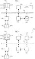
Figure 8 shows an embodiment of a processing system 10a according to the present disclosure.
-
Specifically, the embodiment is essentially based on the embodiment shown in Figure 4 and comprises in addition:
- a communication interface IF_JTAG, preferably a serial communication interface, such as JTAG interface, connected to one or more terminals of the processing system 10a (not shown), such as pins or pads of a respective integrated circuit, in order to receive one or more requests REQ from an external device, such as an external debug device; and
- a verification circuit 130 configured to analyze the request REQ and determine whether the request REQ indicates a request for advancing the life-cycle stage of the processing system 10a.
-
Accordingly, in the embodiment considered, the verification circuit 130 is a separate hardware circuit and the advancing of the life-cycle stage may be requested without an intervention of the processing core(s) 102. Specifically, in various embodiments, the verification circuit 130 is configured to manage only the advancing of the life-cycle stage to the failure analysis stage LC5, while the advancing of the other life-cycle stages (LC1-LC4) may still be managed by the processing core(s) 102, e.g., by receiving respective requests via a CAN interface.
-
Accordingly, in the embodiment considered, the verification circuit 130 generates a signal LCFA_REQ when the request REQ indicates a request to advance the life-cycle stage to the failure analysis stage LC5.
-
More specifically, in the embodiment considered, this signal LCFA REQ is directly provided to the non-volatile memory 104 having stored the life-cycle data LCD, thereby avoiding that the communication has to be transmitted through the communication channel 114.
-
For example, Figure 9 shows an embodiment of the non-volatile memory 104 according to the present disclosure. Specifically, in the embodiment considered, the non-volatile memory 104 comprises:
- one or more physical non-volatile memory areas 1048, such as a plurality of flash memory banks; and
- a control circuit 1040.
-
Specifically, in various embodiments, the control circuit 1040 comprises:
- a security management circuit 1042; and
- a read and write management circuit 1044 configured to manage read and write requests addressed to given memory areas of the non-volatile memory areas 1048.
-
Generally, as shown in Figure 9, the read and write management circuit 1044 may indeed comprise two separate circuits: a read management circuit 1044r configured to manage read requests and a write management circuit 1044w configured to manage write requests.
-
Accordingly, in the embodiment considered, the memory controller 100 receives a read or write request from the communication system 114 and forwards the request to the control circuit 1040. Generally, while shown separately, the memory controller 100 may also form part of the control circuit 1040.
-
Specifically, in various embodiments, the control circuit 1040, in particular the security management circuit 1042, is configured to determine whether the read or write request is permitted. For example, as described in the foregoing, for this purpose the security management circuit 1042 may determine whether the read or write request may access a given memory area based on configuration data CD, in particular the previous mentioned security configuration data SCD, and/or the life-cycle data LCD.
-
For example, for this purpose the control circuit 1040 may have associated a respective configuration data client 112 (with a respective address) and the security configuration data SCP may be provided to the security management circuit 1042 by storing the security configuration data SCP together with the configuration data CD in the non-volatile memory 104, wherein the security configuration data SCP are stored in the memory 104 in the form of DCF data packets also comprising the address of the configuration data client 112 associated with the control circuit 1040. Accordingly, in this way, the configuration circuit 108 will read the configuration data CD and transmit the respective security configuration data SCP to the configuration data client 112 associated with the control circuit 1040.
-
In case the security management circuit 1042 determines that the request is permitted, the security management circuit 1042 forwards the request to the read and write management circuit 1044 (1044r or 1044w), which executes the read or write request.
-
Moreover, in the embodiments considered, the control circuit 1040 comprises a life-cycle program circuit 1046, which is configured to generate a write request to a given memory location of the memory areas 1048 when the signal LCFA_REQ is set. In various embodiments, the life-cycle program circuit 1046 may also verify one or more further conditions COND1, which will be described in greater detail in the following.
-
Additionally or alternatively, as shown in Figure Figure 10, also the verification circuit 130 may generate the signal LCFA REQ not only as a function of the request REQ, but also as a function of one or more conditions COND2.
-
Accordingly, the verification circuit 130 and the life-cycle program circuit 1046 permit to advance the life-cycle stage to the failure analysis stage by using a minimum set of device resources, and bypassing all the protection layers described so far, e.g., the security management circuit 1042. Accordingly, the advancement of the life-cycle stage to the failure analysis stage (and preferably only to this stage) may be accomplished separately with a reduced quantity of circuits involved, thereby reducing the risk that the malfunction of a circuit blocks the advancement of the life-cycle stage. As will be described in greater detail in the following, this mechanism may still guarantee the needed level of security in order to ensure that the advancement cannot be done maliciously, and also the needed level for safety and availability, so that the life-cycle cannot advance to the failure analysis stage during the run-time of the processing system 10a.
-
Accordingly, in the embodiments shown in Figures 8, 9 and 10, two circuits are involved:
- a first circuit 130 (external with respect to the non-volatile memory 104) acting as an initiator of the advancement to the failure analysis stage, which is configured to verify several conditions (in particular the content of the request REQ and the additional conditions COND2) and generate a signal LCFA_REQ indicating an (authorized) request to advance the life-cycle stage to the failure analysis stage; and
- a second circuit 1046 (internal with respect to the non-volatile memory 104), which executes the programming of the non-volatile memory 104 as a function of the signal LCFA REQ.
-
For example, Figures 11 and 12 show a possible embodiment of the verification circuit 130. Specifically, Figure 11 shows an embodiment of a circuit configured to verify the additional conditions COND2 of the verification circuit 130. However, in general, the respective circuit may also be integrated directly within the verification circuit 130.
-
Specifically, as shown in Figure 12, the verification circuit 130 is configured to receive:
- the request REQ provided by the communication interface IF_JTAG; and
- additional conditions COND2 (as shown in Figure 11).
-
Specifically, in various embodiments, the set of input conditions is chosen in order to guarantee security, safety, and availability, e.g., these conditions have to ensure that:
- 1) the operation cannot be start by mistake when the processing system 10a is in use (availability protection);
- 2) it is not be possible to maliciously start the operation (security protection); and
- 3) the operation can only be executed while the processing system 10a is in a safe state (safety protection).
-
For example, in various embodiments, the first condition is verified by monitoring a signal TESTMODE applied to a terminal TP, such as a pin or pad of a respective integrated circuit. For example, in various embodiments, the terminal TP (and thus the signal TESTMODE) is connected to a first logic level, e.g., high, when the processing system 10a is in use. Conversely, in order to ensure that the processing system 10a is not in use, but in a laboratory environment, the verification circuit 130 may verify whether the signal TESTMODE applied to the terminal TP has a second logic level, e.g., low. For example, in order to set the pin TP to low, the processing system 10a has to be removed from the application, e.g., the engine control unit, and connected to some test board. In various embodiments, the terminal TP may also be connected via a pull-up resistor to a supply voltage (i.e., the logic high level), which ensures that an accidental break of the wire connecting the package pin or ball to the pad will not leave the pad at an undefined state. Generally, a pull-down resistor would be used in case the signal TESTMODE is active high, i.e., the test-mode is activated when the terminal TP is connected externally to a logic high level.
-
In various embodiments, the second condition (security) is verified by providing within the verification circuit 130 a
password verification circuit 1300 configured to verify whether the request REQ contains a reference password/keyword RK. Generally, due to the fact that it is assumed that the
processing system 10a is now in a laboratory environment, it is preferable that the password is submitted in the request REQ in plain-text, thus avoiding the need for complex cryptographic operations. Accordingly, in various embodiments, the
circuit 1300 is configured to generate a signal PW_OK when the request REQ provided via the communication interface IF_JTAG corresponds to a given predetermined bit sequence comprising the reference keyword RK. For example, the reference password RK may be hard-wired or stored in the configuration data CD. For example, for this purpose the
verification circuit 130 may have associated a respective configuration data client 112 (with a respective address) and the reference password RK may be provided to the
verification circuit 130 by storing the reference password RK together with the configuration data CD in the
non-volatile memory 104, wherein the reference password RK is stored in the
memory 104 in the form of DCF data packets also comprising the address of the
configuration data client 112 associated with the
verification circuit 130. Accordingly, in this way, the
configuration circuit 108 will read the configuration data CD and transmit the respective reference password RK to the
configuration data client 112 associated with the
verification circuit 130. For example, for a possible implementation of the password verification circuit may be cited European patent application n.
EP 3 432 190 A1 , which is incorporated herein by reference.
-
In various embodiments, the third condition (safety) is verified by ensuring that the processing system 10a is in the reset state, because this is considered by the ISO26262 standard as a safe state.
-
Specifically, as described in the foregoing with respect to Figure 7, by applying a given logic level (e.g., low) to a reset terminal/pin/pad RP, the reset circuit 116 will start the reset procedure at the step 3000. Accordingly, the reset circuit 116 executes the reset and configuration phase CP1 (and optionally the diagnostic phase DP and configuration phase CP2). Moreover, the reset circuit 116 remains at the step 3020 until the logic level at the reset terminal/pin/pad RP is set to a second logic level, (e.g., high).
-
In this respect, as described in the foregoing, the communication interface IF JTAG is active during the step 3022, thus permitting that requests REQ may be sent via the interface IF_JTAG. Due to the fact that the communication interface IF JTAG is usually also active when the processing core(s) are running, the verification circuit 130 is thus configured to determine whether the reset circuit 116 is indeed at the step 3022.
-
For example, in the embodiment considered, the verification circuit 130 receives from the reset circuit 116 a signal RA indicating that the reset module 116 is waiting at the step 3022. In various embodiments, the verification circuit 130 may also monitor the signal ECP indicating that the configuration phase has been completed. For example, in this case, the signal RA may also correspond to the signal at the terminal RP (or its inverted version). In various embodiments, the verification circuit 130 may also verify the signal RM, which distinguishes the first reset phase from the second reset phase.
-
In various embodiments, the verification circuit 130 may also verify whether a given flag is set, which enables or disables the described operation for advancing the life-cycle stage. For example, in the embodiment considered, the verification circuit 130 monitors a signal LCFA_FN provided by a configuration data client 112 associated with the verification circuit 130. Accordingly, the signal LCFA_EN may be generated by storing a respective DCF data packet with the address of this configuration data client to the configuration data CD.
-
For example, in the embodiment shown in Figures 11 and 12, the previous conditions are verified by generating the signal COND2 via a combinational logic circuit 132 as a function of the signals TESTMODE, ECP, LCFA_EN and RA. Conversely, the verification circuit 130 generates the signal LCFA_REQ via a combinational logic circuit 1302 as a function of the signals PW_OK and COND2. Thus, in general, the combinational logic circuits 132 and 1302 may also be combined.
-
In various embodiments, the signal LCFA REQ is stored to a register 1304, preferably a plurality of redundant registers/flip-flops, such as three parallel flip-flops.
-
Accordingly, in various embodiments, the signal LCFA_REQ is only set when:
- the life-cycle advancement to the failure analysis stage is enabled via the signal LCFA EN;
- the processing system 10a is under reset, as indicated, e.g., via the signal RA;
- the configuration data CD and the life-cycle data LCD have been read, as indicated, e.g., via the signal ECP;
- the request REQ corresponds to a valid request, e.g., the correct password RK has been included in the request REQ, as verified via the circuit 1300/indicated via the signal PW OK; and
- the terminal/pin/pad TP has been set to the correct level indicating the test-mode.
-
Accordingly, in the embodiment considered, a user may set the signal LCFA REQ by setting the logic levels at the terminals TP and RP, and sending via the communication interface IF JTAG a given request REQ (with the reference keywork RK) once the configuration phase CP2 has been completed. In fact, due to the fact that the processing core(s) 102 are not yet started, such a request cannot be provided via software, which during this phase is not executed.
-
Specifically, in various embodiments, the register(s)/flip-flop(s) 1304 are only reset in response to the reset generated at the step 3002, but not in response to the reset at the step 3014. For example, as shown in Figure 12, the register/flip-flop 1304 may be configured to:
- reset the signal LCFA_REQ when the signal RESET is set and the signal RM has the first logic level set at the step 3002 (e.g., high); and
- inhibit the reset of the signal LCFA REQ when the signal RESET is set and the signal RM has the second logic level set at the step 3016 (e.g., low).
-
Alternatively, the register/flip-flop 1304 may be reset only in response to the reset signal RESET1 (generated at the step 3002/destructive reset DR) and not the reset signal RESET2 (generated at the step 3016/functional reset FR).
-
In various embodiments, the signal LCFA REQ is also provided to the reset circuit 116. The operation of this feedback will be described in greater detail in the following with respect to the life-cycle program circuit 1046.
-
Before going into the details of the life-cycle program circuit 1046, it is worthwhile to briefly describe how data may be programmed to a non-volatile memory, such as a flash memory.
-
Generally, writing data to a non-volatile memory is more complex than writing data to a RAM, where one single write instruction moves some data directly in the RAM and the data is then immediately latched in the memory. Conversely, in the case of the non-volatile memory, the programming requires usually a sequence of operations.
-
For example, in order to program a non-volatile memory, it may be required that the supply voltage of the memory is set to a higher voltage. This may involve a given time until the voltage settles to the new value. Similarly, the higher voltage should be removed once the programming operation is completed. Moreover, a single programming/write operation may indeed involve a complex sequence of micro-operation to control the whole programming operation. The reason is that for the non-volatile memory, undesired analog effects, which can be different depending on the non-volatile memory technology being used, might hinder the successful completion of the programming operation.
-
For example, in the case of a Flash memory, a cell might become "depleted", which is a condition where the cell has lost its trapped charge: in such a case the cell drives an excessive flow of current along its connected bit-line and it would be extremely difficult to recover the cell and bring it to a programmed state. As a matter of fact, dedicated algorithms might be needed in order to restore a depleted cell.
-
Accordingly, typically, a processing core 102 has to execute a sequence of operations in order to write data to the non-volatile memory 104. For example, in various embodiments, a processing core 102 may be configured to execute the following steps for programing data to the non-volatile memory 104:
- 1) configure the non-volatile memory 104 so that it is in a programming mode;
- 2) provide the data to be programmed (via the memory controller 100) to the non-volatile memory 104;
- 3) set the supply voltage of the non-volatile memory 104 to a higher (write) voltage;
- 4) wait until the programming operation is completed
- 5) set the supply voltage of the non-volatile memory 104 to a lower (read) voltage;
- 6) perform a read operation of the non-volatile memory 104 (via the memory controller 100) in order to verify whether the data have been programmed correctly; and
- 7) configure the non-volatile memory 104 so that it is in the normal operation mode.
-
Typically, the above operations are performed by sending via software instructions requests from the processing core 102 to the control circuit 1040. For example, for this purpose, the control circuit 1040 may also manage a register interface, wherein each register (such as a write data register, a read data register, an address register and a control register) may have associated a respective address.
-
For example, during the fourth step is performed the real programming operation of the memory area 1048. During this step, the software may just wait until the non-volatile memory 104 has completed the programming. From the software point of view, this is just a simple wait step, but in reality, during this timeframe the non-volatile memory 104 executes a complex sequence of micro-operations, like giving a short voltage pulse, then comparing the current cell with a reference cell, give another pulse if the current is not the target one and so on. Often an unbalance ratio in the cell V-I (voltage-current) characteristic is applied between the cell being programmed and the reference, so that the end of the operation, which is marked by the fact that the current of the programmed cell has reached a sufficient distance from the current of the reference cell, gives even more margin (in terms of current distance between the programmed and the reference cell) when an unbalanced V-I ratio is used during a read operation. Those of skill in the art will appreciate that this is a simplification of the programming operation of the non-volatile memory, and in reality, the internal sequence of operations might be more complex, depending on the type of technology adopted for the non-volatile memory.
-
Accordingly, the write management circuit 1044w has to execute a sequence of micro-operations in order to implement the programming operation.
-
For this purpose, the write management circuit 1044w may be implemented with a hardware finite state machine or a microprocessor being programmed via software instructions. For example, the microprocessor may have associated a programmable voltage source for setting the supply voltage of the memory areas 1048, and an analog-to-digital converter for monitoring the voltage of a given cell of the memory area 1048, etc. For example, the use of a microprocessor is particularly useful in order to permit an improvement of the programming operation. For example, such a microprocessor permits to use different sequences (at least during the development stage) or update the different sequence even later. Such sequences of micro-operations, executed by a microprocessor, is typically called "embedded-algo".
-
Hence, a microprocessor provides more flexibility than a fixed state machined. Such a microprocessor may only be used to manage the more complex write operations, while the read operation may still be performed via a dedicated hardware circuit 1044r. In fact, while a microprocessor provides more flexibility, such a microprocessor usually has a higher power-consumption than a dedicated hardware circuit. For this reason, the microprocessor (but a similar issue may also exist for a complex state machine 1044w managing the write operation) is typically switched off (or at least suspended) during read operations. In fact, during run-time, the non-volatile memory 104 is mainly read and rarely written. For example, when a processing core 102 activates the programming mode of the non-volatile memory 104, indeed this step may switch on the write circuit/microprocessor 1044w of the non-volatile memory 104.
-
However, this may imply that also the life-cycle programming circuit 1046 has to activate in some way the write circuit 1044w, e.g., the respective microprocessor. In fact, as mentioned before, usually the control circuit 1040 activates the write circuit 1044w only in response to one or more commands received from the memory controller 100. For example, in various embodiments, the control circuit 1040 is configured to activate the write circuit 1044w only when:
- a first request is received, wherein the first request activates the programming mode, e.g., by setting a bit of a control register of the control circuit 1040; and
- a second request is receiver, wherein the second request provides the data to be written, e.g., by storing the data to a write-data register of the control circuit 1040.
-
For example, this permits to avoid that the write circuit 1044w is activated due to an erroneous (isolated) first request or second request.
-
Accordingly, in various embodiments, also the life-cycle programming circuit 1046 has to activate in some way write circuit 1044w in order to program the non-volatile memory areas 1048. Accordingly, the life-cycle programming circuit 1046 could execute the above-mentioned operations for starting the write circuit 1044.
-
Conversely, in various embodiments of the present disclosure the above-described feedback of the signal LCFA REQ to the reset circuit 116 is used for this purpose.
-
Specifically, in various embodiments, during a destructive or functional reset at the steps 3002 or 3014, also the circuit implementing the write circuit 1044w, such as a microprocessor or a state machine, is activated, e.g., in order to executes several internal initializations, and then the circuit is deactivated, i.e., in various embodiments, the circuit implementing the write circuit 1044w is activated in response to the reset generate at the step 3002 and the reset generated at the step 3014, and once the non-volatile memory 104 is initialized, the circuit implementing the write circuit 1044 is deactivated.
-
However, as described with respect to Figure 7, following the reset at the step 3002, the reset circuit 116 activates the configuration phase CP1 during which the configuration data CD and life-cycle data LCD are read. Only once the configuration data have been read, possibly also executing the diagnostic phase DP, the further reset 3014 and the further configuration phase CP2, it is possible to maintain the processing system 10a in the reset stage via the signal at the reset terminal RP. Thus, when the request REQ may be sent via the communication interface IF JTAG and the verification circuit 130 verified the request REQ and the additional conditions COND2, the circuit implementing the write circuit 1044w may indeed be already deactivated.
-
In this respect, as mentioned before, the register(s)/flip-flops(s) 1304 are configured to be reset only in response to the reset at the step 3002/destructive reset DR, while the register(s)/flip-flops(s) 1304 maintain their values in response to a reset at the step 3014/functional reset FR. Thus, the circuit implementing the write circuit 1044w may be activated by starting a functional reset FR at the step 3014, i.e., the reset circuit 116 is configured to start a functional reset at the step 3014 in response to the signal LCFA_REQ being set. Optionally, the reset circuit 116 may also verify additional conditions, such as the logic level of the terminal TP and/or the terminal RP (see the respective description of the verification circuit 130).
-
Accordingly, when starting the reset procedure at the step 3014, the register(s)/flip-flops(s) 1304 are not reset, but the circuit implementing the write circuit 1044w is activated.
-
Accordingly, in various embodiments, the circuit implementing the write circuit 1044w may be configured to verify the signal LCFA _REQ when the circuit is activated, e.g., in response to a reset. Moreover, in response to determining that the signal LCFA REQ is set, the write circuit 1044w may perform the programming of the life-cycle data LCD in the memory area 1048 in order to advance the life-cycle stage to the failure analysis stage.
-
Specifically, once the processing system 10a is switched on, the reset circuit 116 will execute the reset at the step 3002 and start the configuration phase CP1 (and optionally the diagnostic phase DP, the second reset at the step 3014 and the second configuration phase CP2). Accordingly, when the circuit implementing the write circuit 1044w is initialized in response to the reset at the step 3002 (and optionally the reset at the step 3014), the signal LCFA_REQ is not set (e.g., is low).
-
Next, when the verification circuit 130 sets the signal LCFA_REQ, this signal will also trigger a new reset at the step 3014. Specifically, as mentioned before, in the embodiment considered, the register 1304 maintains its content during the reset at the step 3014.
-
Thus, when the circuit implementing the write circuit 1044w is initialized in response to the reset at the step 3014, the signal LCFA_REQ is now set (e.g., is high).
-
Figure 13 shows in this respect a possible embodiment of the programming circuit 1046. Generally, as mentioned before, the signal LCFA_REQ may also be provided directly to the write circuit 1044, i.e., the programming circuit 1046 is purely optional.
-
However, as shown in Figure 13, the additional programming circuit 1046 may be used:
- in case the signal LCFA REQ indeed is provided by a plurality of registers/flip-flops, to generate via a circuit 1052 a signal LCFA_REQ' by combining the signals LCFA_REQ, e.g., by setting the signal LCFA_REQ' to the bit value of the majority of the values of the signals LCFA_REQ, such as a triple-vote decision; and/or
- to determine via circuits 134 and 1050 a signal FCFA not only as a function of the signal LCFA_REQ (or the signal LCFA_REQ') but also as a function of one or more optional further conditions COND1.
-
For example, the programming circuit 1046 may verify via the combinational logic circuits 134 and 1050 at least one of:
- the logic level of the terminal TP (i.e., the signal TESTMODE) and/or the terminal RP (see the respective description of the verification circuit 130); and/or
- whether the circuit implementing the write circuit 1044 has been activated in response to the functional reset FM at the step 3014, e.g., by verifying the logic value of the signal RM
-
For example, in various embodiments, the programming operation of the life-cycle data LCD is only started, when the write circuit determines during an initialization phase, e.g., via the programming circuit 1046, the following conditions:
- the majority of bits of the signal LCFA_REQ are set; and
- the signal TESTMODE applied to the terminal TP is set.
-
Generally, while not shown in Figure 13, the signal LCFA_REQ, LCFA REQ' and/or LCFA may be provided to a register interface of the microprocessor 1044w, e.g., the so called Special-Function Registers (SFR) of the microprocessor implementing the write circuit 1044w. Generally, while the verification of the additional conditions COND1 is shown via hardware combinational circuits 134 and/or 1050, indeed at least part of these verifications may be performed via software instructions. Similarly, also the operation of the (voting) circuit 1052 may be performed via software instructions executed by the microprocessor 1044.
-
Generally, even in a software implementation may be used a dedicated voting circuit 1052, because indeed the signal LCFA_REQ' may be used to signal the reset request to the reset module 116, i.e., the reset circuit 116 may be configured to start the functional reset in response to the signal LCFA REQ' (rather than the signal LCFAREQ). For example, in this case, a similar voting circuit may be implemented directly in the reset circuit 116.
-
Accordingly, in various embodiments, the circuit 1052 may correspond to the register interface of the microprocessor implementing the write circuit 1044w, thereby providing directly the signals LCFA_REQ (provided by the registers 1304) to the microprocessor. In fact, preferably the voting of the signals LCFA REQ and at least the combination with the additional conditions at the circuit 1050 (and optionally also the operation of the circuit 134) is performed directly via software instructions. The reason to have all signals LCFA_REQ mirrored into respective register bits (e.g., 3) of the microprocessor 1044 is to protect this mechanism from a spurious activation, which would be catastrophic for the application because the device will enter the failure analysis stage, where the application would not run anymore. However, in various embodiments, the microprocessor within the non-volatile memory 104 is not classified as an ASIL-D component, according to ISO26262 specification, and it can eventually fail. Conversely, an ASIL-D microprocessor would cost additional area and power. Thus, by reading a plurality of separate bits of the signal LCFA_REQ and implementing the voting via software instructions, such as a triple-vote decision, the probability to have a failure is significantly reduced.
-
As mentioned before, when the functional reset at the step 3014 is triggered in response to the signal LCFA_REQ, the non-volatile memory 104 starts its own initialization again and during this time the request for advancing the life-cycle stage to the failure analysis stage is activated, because the signal LCFA_REQ maintains its value.
-
In this respect, no additional information is required to advance the life-cycle stage to the failure analysis stage, because:
- the memory location of the life-cycle data LCD in the non-volatile memory 1048 is fixed; and
- the signature to be programmed in order to advance the life-cycle stage to the failure analysis stage is also fixed.
-
As described in the foregoing, it is not particularly relevant how the life-cycle data LCD are encoded. For example, it is sufficient that a given bit sequence is associated with a sub-set of bits associated with the failure analysis stage. Accordingly, by programming the respective subset of bits, the life-cycle stage may be advanced to the failure analysis stage, irrespective of the previous life-cycle stage. However, when using more complex encoding schemes, the write circuit 1044 could also read first the old life-cycle data LCD.
-
Generally, once the write circuit 1044 has completed the programming of the life-cycle data LCD, it is required that the processing circuit 10a reads again the life-cycle data LCD. However, it is also necessary to reset the signal(s) LCFA_REQ. For example, in various embodiments this is achieved by performing a new reset starting at the step 3000, thus executing at the step 3002 a reset of the register(s) 1304.
-
Generally, the new reset may also be performed manually, e.g.:
- once having sent the correct request REQ, the user may wait a given time, e.g., more than 1 s, whereby the write circuit 1044w completes the programming operation of the life-cycle data LCD;
- de-assert the signal at the reset terminal RP; and
- assert the signal at the reset terminal RP again, thereby starting a new reset at the step 3000.
-
Thus, in various embodiments, the advancement of the lift-cycle stage may involve:
- 1) activating a destructive reset via the terminal RP (step 3002);
- 2) in response to the destructive reset DR, the configuration module 108 reads the configuration data CD and life-cycle data LCD (configuration phase CP1), and optionally performs the other operations until the step 3020;
- 3) once the configuration phase CP1 and optionally CP2 has been terminated, the verification circuit is activated;
- 4) in order to have sufficient time to submit the request, the reset terminal remains set (step 3020);
- 5) the request REQ is submitted with the correct password;
- 6) once the request REQ is verified, the signals LCFA_REQ are set;
- 7) the signals LCFA REQ are used to generate a functional reset of the processing system 10a (step 3016);
- 8) in response to the functional reset, the circuit implementing the write circuit 1044w is activated and executes its initialization;
- 9) the circuit implementing the write circuit 1044w reads the signals LCFA REQ during the initialization;
- 10) the write circuit 1044w and/or programming circuit 1046 verifies whether the majority of the bits of the signals LCFA_REQ are set;
- 11) due to the fact that the signals LCFA REQ are set, the write circuit 1044w writes the life-cycle data LCD in order to advance to the failure analysis stage; and
- 12) a new destructive reset is started manually or automatically (step 3002).
-
Generally, instead of activating the circuit implementing the write circuit 1044w indirectly by generating a reset in response to the signal(s) LCFA_REQ (or the signal LCFA_REQ'), the circuit implementing the write circuit 1044w may also be activate in other ways in response to setting the signal(s) LCFA_REQ. For example, the circuit implementing the write circuit 1044w may be activated directly in response to the signal(s) LCFA_REQ or the signal LCFA_REQ', e.g., by configuring the respective signal(s) as wake-up signals of the circuit implementing the write circuit 1044w.
-
Accordingly, the present disclosure proposes a new scheme to easily advance a failing device to the failure analysis stage, bypassing most of the circuitry ordinarily involved for advancing the life-cycle stage. By adopting the solution proposed, the advancement to the failure analysis stage is guaranteed with a higher probability compared to the standard methodology of life cycle programming via application software. The solution adopted does not compromise the overall security as it allows the life-cycle advancement only upon a successful challenge of a secret password. In addition, the proposed solution does not compromise the safety, because the operation is executed only during the reset phase, which is considered by ISO26262 standard a safe state. Finally, the proposed solution does not comprise the availability because a set of conditions are put in place in order to avoid any spurious activation of the live-cycle advancement.
-
Of course, without prejudice to the principle of the invention, the details of construction and the embodiments may vary widely with respect to what has been described and illustrated herein purely by way of example, without thereby departing from the scope of the present invention, as defined by the ensuing claims.
-
For example, while in the foregoing has been described a mechanism in order to advance the life-cycle stage to the failure analysis stage, modern processing systems may alternatively or additionally comprise a test life-cycle stage. Compared to the failure analysis stage, the test life-cycle stage has usually a reduced influence on the overall security. Thus, instead of advancing to the failure analysis stage, the write circuit 1044 could also advance to the test life-cycle stage. In fact, what is relevant for the present disclosure is that a separate mechanism is used to advance the life-cycle stage to a stage wherein reduced security mechanisms are active than in the in-field stage.