EP4019985A1 - Detection circuit for instantaneous voltage drop and vehicle-mounted diagnostic system - Google Patents
Detection circuit for instantaneous voltage drop and vehicle-mounted diagnostic system Download PDFInfo
- Publication number
- EP4019985A1 EP4019985A1 EP20855013.7A EP20855013A EP4019985A1 EP 4019985 A1 EP4019985 A1 EP 4019985A1 EP 20855013 A EP20855013 A EP 20855013A EP 4019985 A1 EP4019985 A1 EP 4019985A1
- Authority
- EP
- European Patent Office
- Prior art keywords
- resistor
- circuit
- comparator
- detection circuit
- determination unit
- Prior art date
- Legal status (The legal status is an assumption and is not a legal conclusion. Google has not performed a legal analysis and makes no representation as to the accuracy of the status listed.)
- Granted
Links
- 238000001514 detection method Methods 0.000 title claims abstract description 73
- 239000003990 capacitor Substances 0.000 claims abstract description 56
- 238000004146 energy storage Methods 0.000 claims abstract description 25
- 238000006243 chemical reaction Methods 0.000 claims description 7
- 238000010586 diagram Methods 0.000 description 7
- 230000008859 change Effects 0.000 description 2
- 238000007599 discharging Methods 0.000 description 2
- 230000000694 effects Effects 0.000 description 2
- 230000006872 improvement Effects 0.000 description 2
- 238000004519 manufacturing process Methods 0.000 description 2
- 230000004048 modification Effects 0.000 description 2
- 238000012986 modification Methods 0.000 description 2
- 208000032365 Electromagnetic interference Diseases 0.000 description 1
- 230000003247 decreasing effect Effects 0.000 description 1
- 239000000446 fuel Substances 0.000 description 1
- 230000006870 function Effects 0.000 description 1
- 238000012423 maintenance Methods 0.000 description 1
- 238000012544 monitoring process Methods 0.000 description 1
Images


Classifications
-
- G—PHYSICS
- G01—MEASURING; TESTING
- G01R—MEASURING ELECTRIC VARIABLES; MEASURING MAGNETIC VARIABLES
- G01R17/00—Measuring arrangements involving comparison with a reference value, e.g. bridge
- G01R17/02—Arrangements in which the value to be measured is automatically compared with a reference value
-
- B—PERFORMING OPERATIONS; TRANSPORTING
- B60—VEHICLES IN GENERAL
- B60R—VEHICLES, VEHICLE FITTINGS, OR VEHICLE PARTS, NOT OTHERWISE PROVIDED FOR
- B60R16/00—Electric or fluid circuits specially adapted for vehicles and not otherwise provided for; Arrangement of elements of electric or fluid circuits specially adapted for vehicles and not otherwise provided for
- B60R16/02—Electric or fluid circuits specially adapted for vehicles and not otherwise provided for; Arrangement of elements of electric or fluid circuits specially adapted for vehicles and not otherwise provided for electric constitutive elements
- B60R16/023—Electric or fluid circuits specially adapted for vehicles and not otherwise provided for; Arrangement of elements of electric or fluid circuits specially adapted for vehicles and not otherwise provided for electric constitutive elements for transmission of signals between vehicle parts or subsystems
- B60R16/0231—Circuits relating to the driving or the functioning of the vehicle
- B60R16/0232—Circuits relating to the driving or the functioning of the vehicle for measuring vehicle parameters and indicating critical, abnormal or dangerous conditions
-
- G—PHYSICS
- G01—MEASURING; TESTING
- G01R—MEASURING ELECTRIC VARIABLES; MEASURING MAGNETIC VARIABLES
- G01R19/00—Arrangements for measuring currents or voltages or for indicating presence or sign thereof
- G01R19/0038—Circuits for comparing several input signals and for indicating the result of this comparison, e.g. equal, different, greater, smaller (comparing pulses or pulse trains according to amplitude)
-
- G—PHYSICS
- G01—MEASURING; TESTING
- G01R—MEASURING ELECTRIC VARIABLES; MEASURING MAGNETIC VARIABLES
- G01R19/00—Arrangements for measuring currents or voltages or for indicating presence or sign thereof
- G01R19/165—Indicating that current or voltage is either above or below a predetermined value or within or outside a predetermined range of values
- G01R19/16533—Indicating that current or voltage is either above or below a predetermined value or within or outside a predetermined range of values characterised by the application
- G01R19/16538—Indicating that current or voltage is either above or below a predetermined value or within or outside a predetermined range of values characterised by the application in AC or DC supplies
- G01R19/16542—Indicating that current or voltage is either above or below a predetermined value or within or outside a predetermined range of values characterised by the application in AC or DC supplies for batteries
-
- G—PHYSICS
- G01—MEASURING; TESTING
- G01R—MEASURING ELECTRIC VARIABLES; MEASURING MAGNETIC VARIABLES
- G01R31/00—Arrangements for testing electric properties; Arrangements for locating electric faults; Arrangements for electrical testing characterised by what is being tested not provided for elsewhere
- G01R31/005—Testing of electric installations on transport means
- G01R31/006—Testing of electric installations on transport means on road vehicles, e.g. automobiles or trucks
-
- G—PHYSICS
- G07—CHECKING-DEVICES
- G07C—TIME OR ATTENDANCE REGISTERS; REGISTERING OR INDICATING THE WORKING OF MACHINES; GENERATING RANDOM NUMBERS; VOTING OR LOTTERY APPARATUS; ARRANGEMENTS, SYSTEMS OR APPARATUS FOR CHECKING NOT PROVIDED FOR ELSEWHERE
- G07C5/00—Registering or indicating the working of vehicles
- G07C5/08—Registering or indicating performance data other than driving, working, idle, or waiting time, with or without registering driving, working, idle or waiting time
- G07C5/0808—Diagnosing performance data
-
- G—PHYSICS
- G08—SIGNALLING
- G08B—SIGNALLING OR CALLING SYSTEMS; ORDER TELEGRAPHS; ALARM SYSTEMS
- G08B21/00—Alarms responsive to a single specified undesired or abnormal condition and not otherwise provided for
- G08B21/18—Status alarms
- G08B21/182—Level alarms, e.g. alarms responsive to variables exceeding a threshold
-
- Y—GENERAL TAGGING OF NEW TECHNOLOGICAL DEVELOPMENTS; GENERAL TAGGING OF CROSS-SECTIONAL TECHNOLOGIES SPANNING OVER SEVERAL SECTIONS OF THE IPC; TECHNICAL SUBJECTS COVERED BY FORMER USPC CROSS-REFERENCE ART COLLECTIONS [XRACs] AND DIGESTS
- Y02—TECHNOLOGIES OR APPLICATIONS FOR MITIGATION OR ADAPTATION AGAINST CLIMATE CHANGE
- Y02T—CLIMATE CHANGE MITIGATION TECHNOLOGIES RELATED TO TRANSPORTATION
- Y02T10/00—Road transport of goods or passengers
- Y02T10/10—Internal combustion engine [ICE] based vehicles
- Y02T10/40—Engine management systems
Definitions
- Embodiments of the present invention relate to the technical field of detection, and in particular, to a detection circuit for instantaneous voltage drop and an on-board diagnostic system.
- the system is used for monitoring the operating condition of an engine and the operating state of an exhaust post-treatment system at any time. Once it is found that an excessive emission situation possibly occurs, a warning is sent immediately.
- the OBD can monitor, in real time, operating data such as whether a vehicle is ignited, whether the vehicle is speeding and whether the fuel consumption is excessively high, and can analyze whether a fault occurs. If the system fails, a fault light or an engine-checking warning light is turned on; and the OBD system stores the fault information in a memory, and related information may be read in the form of fault codes by means of a standard diagnostic instrument and diagnostic interface. According to prompt of the fault codes, a maintenance personnel can quickly and accurately determine the nature and position of the fault.
- the OBD ensures the safety of travel of the vehicle, and records conditions of the vehicle.
- Embodiments of the present invention provide a detection circuit for instantaneous voltage drop and an on-board diagnostic system.
- Embodiments of the present invention provide a detection circuit for instantaneous voltage drop, comprising: two RC circuits, a comparator and a determination unit; each RC circuit comprises a first resistor, a second resistor and an energy storage capacitor; a first end of the first resistor is configured to receive a to-be-detected voltage, a second end of the first resistor is connected to a first end of the second resistor, and a second end of the second resistor is grounded; the energy storage capacitor is connected in parallel with the second resistor; the first end of the second resistor forms an output end of the RC circuit; the output ends of the two RC circuits are correspondingly connected to two input ends of the comparator, respectively; an output end of the comparator is connected to the determination unit; wherein in the two RC circuits, resistance ratios of the second resistors to the first resistors are different, capacitances of the energy storage capacitors are different, and the capacitance of the energy storage capacitor in the RC circuit with a larger resistance
- Embodiments of the present invention further provide an on-board diagnostic system, comprising: the described detection circuit for instantaneous voltage drop.
- a first embodiment of the present invention relates to a detection circuit for instantaneous voltage drop, which can be applied to voltage detection in any scenarios where a voltage may drop instantaneously; for example, when a vehicle is ignited, the voltage of a power source for supplying power to an ignition device will drop instantaneously, and therefore the circuit of some embodiments of the present invention can be used for detecting whether the vehicle is ignited.
- the scenarios are not limited in this embodiment.
- the detection circuit for instantaneous voltage drop in some embodiments of the present invention can be applied to any scenarios in which it is required to detect whether a voltage drops instantaneously.
- the detection circuit for instantaneous voltage drop comprises: two RC circuits, a comparator 13 and a determination unit 14, the two RC circuits being respectively denoted as a first RC circuit 11 and a second RC circuit 12.
- Each RC circuit comprises a first resistor, a second resistor and an energy storage capacitor.
- the first resistors in the two RC circuits are respectively denoted by reference signs R1 and R2, and hereinafter are respectively referred to as a resistor R1 and a resistor R2 for short;
- the second resistors in the two RC circuits are respectively denoted by reference signs R3 and R4, and hereinafter are respectively referred to as a resistor R3 and a resistor R4 for short;
- the energy storage capacitors in the two RC circuits are respectively denoted by reference signs C1 and C2, and hereinafter are respectively referred to as a capacitor C1 and a capacitor C2 for short.
- a first end of the resistor R1 is used for receiving a to-be-detected voltage VBATT, a second end of the resistor R1 is connected to a first end of the resistor R3, and a second end of the resistor R3 is grounded; the capacitor C1 is connected in parallel with the resistor R3; and a first end of the resistor R3 forms an output end OUT1 of the first RC circuit 11.
- a first end of the resistor R2 is used for receiving the to-be-detected voltage VBATT, a second end of the resistor R2 is connected to a first end of the resistor R4, and a second end of the resistor R4 is grounded; the capacitor C2 is connected in parallel with the resistor R4; and a first end of the resistor R4 forms an output end OUT2 of the second RC circuit 12.
- Output ends OUT1 and OUT2 of the two RC circuits are correspondingly connected to two input ends of the comparator 13 respectively, and an output end of the comparator 13 is connected to the determination unit 14.
- the resistance ratios of the second resistors to the first resistors in the two RC circuits are different, which means that the resistance ratio of the resistor R3 to the resistor R1 in the first RC circuit 11 is different from the resistance ratio of the resistor R4 to the resistor R2 in the second RC circuit 12.
- both the resistor R1 and the resistor R3 have a voltage division function, and the voltage outputted by the output end OUT1 is the voltage across two ends of the resistor R3; and by the same reasoning, in the second RC circuit 12, the voltage outputted by the output end OUT2 is the voltage across two ends of the resistor R4.
- the to-be-detected voltage VBATT is inputted to both the first end of the resistor R1 and the first end of the resistor R2, that is, input voltages of the first RC circuit 11 and the second RC circuit 12 are the same.
- the resistance ratio of the resistor R3 to the resistor R1 is different from the resistance ratio of the resistor R4 to the resistor R2, which indicates that when the input voltages of the first RC circuit 11 and the second RC circuit 12 are the same, the voltage allocated to the resistor R3 in the first RC circuit 11 is different from the voltage allocated to the resistor R4 in the second RC circuit 12. Therefore, voltages received by the two input ends of the comparator 13 are also different.
- the capacitances of the energy storage capacitors in the two RC circuits are different, which means that the capacitance of the capacitor C1 in the first RC circuit 11 is different from the capacitance of the capacitor C2 in the second RC circuit 12. Therefore, an RC discharge curve of the first RC circuit 11 is different from an RC discharge curve of the second RC circuit 12, that is, during discharging, the RC circuit with a larger capacitor capacitance discharges faster.
- the capacitance of the energy storage capacitor in the RC circuit with a larger resistance ratio of the second resistor to the first resistor is less, which means that if the resistance ratio of the resistor R3 to the resistor R1 in the first RC circuit 11 is greater than the resistance ratio of the resistor R4 to the resistor R2 in the second RC circuit 12, the capacitance of the energy storage capacitor in the first RC circuit 11 is less than the capacitance of the energy storage capacitor in the second RC circuit 12; and if the resistance ratio of the resistor R3 to the resistor R1 in the first RC circuit 11 is less than the resistance ratio of the resistor R4 to the resistor R2 in the second RC circuit 12, the capacitance of the energy storage capacitor in the first RC circuit 11 is greater than the capacitance of the energy storage capacitor in the second RC circuit 12.
- the determination unit 14 is configured to determine that the to-be-detected voltage drops instantaneously upon detection that the comparator 13 is inverted.
- the determination unit 14 may be a processing chip, for example, a main control chip of the on-board diagnostic system where the ignition device is located.
- the present invention is not limited thereto, and the determination unit 14 may also be implemented by a hardware circuit.
- the output end OUT1 of the first RC circuit 11 is connected to a non-inverting input end of the comparator 13, and the output end OUT2 of the second RC circuit 12 is connected to an inverting input end of the comparator 13; and the resistance ratio of the resistor R3 to the resistor R1 is less than the resistance ratio of the resistor R4 to the resistor R2, and the capacitance of the capacitor C1 is greater than the capacitance of the capacitor C2.
- the capacitor C1 may be designed as a first sub-capacitor C1_1 and a second sub-capacitor C1_2 connected in parallel, wherein the capacitance of the first sub-capacitor C1-1 is the same as the capacitance of the capacitor C2, so as to satisfy that the capacitance of the capacitor C1 is greater than the capacitance of the capacitor C2.
- the resistor R3 and the resistor R4 may be set as two resistors having the same resistance value, and the resistance value of the resistor R1 is greater than the resistance value of the resistor R2, so as to satisfy that the resistance ratio of the resistor R3 to the resistor R1 is less than the resistance ratio of the resistor R4 to the resistor R2.
- the resistance ratio of the resistor R3 to the resistor R1 is less than the resistance ratio of the resistor R4 and the resistor R2, and input voltages of the first RC circuit 11 and the second RC circuit 12 are both the to-be-detected voltage VBATT, and thus the voltage allocated to the resistor R3 in the first RC circuit 11 is less than the voltage allocated to the resistor R4 in the second RC circuit 12.
- the voltage V+ received by the non-inverting input end of the comparator 13 is the voltage outputted by the output end OUT1
- the voltage V- received by the inverting input end of the comparator is the voltage outputted by the output end OUT2
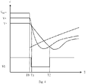
- the voltage V+ received by the non-inverting input end of the comparator 13 is less than the voltage V- received by the inverting input end, and thus an output voltage W1 of an output end of the comparator 13 is a low-level signal, as shown in Fig. 3 .
- the capacitance of the capacitor C1 is greater than the capacitance of the capacitor C2, and thus before the vehicle is ignited, the quantity of electric charge stored in the capacitor C1 is greater than the quantity of electric charge stored in the capacitor C2, and the discharge duration of the capacitor C1 is longer than the discharge duration of the capacitor C2. Therefore, the drop speed of the voltage across two ends of the resistor R3 is slower than the drop speed of the voltage across two ends of the resistor R4, and the drop speed of the voltage V+ received by the non-inverting input end of the comparator 13 is less than the drop speed of the voltage V- received by the inverting input end, so that starting from time T1 as shown in Fig.
- the determination unit 14 can determine that the to-be-detected voltage VBATT drops instantaneously, that is, the vehicle is ignited.
- the voltage of a power supply source of the ignition device will increase, that is, the to-be-detected voltage VBATT will increase back to a steady state, and therefore the voltages outputted by the output end OUT1 and the output end OUT2 will also slowly increase and tend to a steady state, and the voltage (i.e., the voltage V+ received by the non-inverting input end of the comparator 13) outputted by the output end OUT1 will be less than the voltage(i.e., the voltage V- received by the inverting input end of the comparator 13) outputted by the output end OUT2 again.
- this time represents a time at which the voltage V+ recovers to be less than the voltage V-, and at this time, the output voltage W1 of the output end of the comparator 13 is a low-level signal.
- the output end OUT1 of the first RC circuit 11 is connected to the inverting input end of the comparator 13
- the output end OUT1 of the second RC circuit 12 is connected to the non-inverting input end of the comparator 13
- all the resistance values of the resistors and the capacitances of the capacitors are the same as those in the example in Fig. 3 , and then the implementation principle thereof is substantially the same as that of the example in Fig. 3 , and the difference merely lies in that: as shown in Fig.
- the determination unit 14 can determine that the to-be-detected voltage VBATT drops instantaneously, that is, the vehicle is ignited. After the ignition is completed, the to-be-detected voltage VBATT increases to a steady state, that is, after the time T2, the output voltage W1 of the output end of the comparator 13 is a high-level signal.
- the resistance ratios of the second resistors to the first resistors in the two RC circuits are different, and thus after voltage division, the magnitudes of the voltages inputted to the two input ends of the comparator are different, and their relative magnitude remains unchanged in the steady state; wherein the voltage inputted, to the comparator, by the RC circuit with a larger resistance ratio of the second resistor to the first resistor is larger.
- the capacitances of the energy storage capacitors in the two RC circuits are different, such that the discharge durations of the energy storage capacitors in the two RC circuits are different.
- the capacitance of the energy storage capacitor in the RC circuit with a larger resistance ratio of the second resistor to the first resistor is smaller, and thus when the to-be-detected voltage drops instantaneously, the discharge duration of the RC circuit inputting a larger voltage to the comparator is shorter, while the discharge duration of the RC circuit inputting a smaller voltage to the comparator is longer, such that at a certain time after the to-be-detected voltage drops instantaneously, the relative magnitude of the voltages inputted to the two input ends of the comparator changes, and thus the comparator is inverted. Therefore, whether the to-be-detected voltage drops instantaneously can be determined on the basis whether the comparator is inverted. Furthermore, the detection circuit in some embodiments of the present invention has a simple structure, a small layout, low cost and a high detection speed.
- detecting whether ignition occurs upon detection that the comparator is inverted, it can be determined that the to-be-detected voltage drops instantaneously, that is, as shown in time T1 in Figs.3 and 4 , it can be detected that the comparator is inverted.
- detecting that the battery voltage at a later time is higher refers to a time when the battery voltage will increase again after the ignition, that is, after the time T2 shown in Figs.
- the circuit in this embodiment can further comprise a connector 15.
- the connector 15 is configured to acquire the to-be-detected voltage VBATT from a power source and input the to-be-detected voltage VBATT into the two RC circuits.
- the to-be-detected voltage VBATT needs to be acquired from the power supply source of the ignition device, and the connector 15 is, for example, an OBD interface of the vehicle.
- the type of the connector 15 needs to be set.
- the circuit in this embodiment can further comprise an ESD (electrostatic) and EMI (electromagnetic) protection circuit 16, provided between the connector 15 and the RC circuits, and functioning to isolate electrostatic and electromagnetic interferences.
- a second embodiment of the present invention relates to a detection circuit for instantaneous voltage drop.
- the second embodiment is substantially the same as the first embodiment, and the main difference lies in that: in the second embodiment of the present invention, as shown in Fig. 6 , the detection circuit further comprises two diodes VT1 and VT2, and the first ends of the first resistors in the two RC circuits are correspondingly connected to the two diodes respectively, so as to receive the to-be-detected voltage by means of the diodes.
- a first end of the resistor 1 in the first RC circuit 11 is connected to a cathode of the diode VT1
- a first end of the resistor 2 in the second RC circuit 12 is connected to a cathode of the diode VT2
- anodes of the diodes VT1 and VT2 are both connected to the ESD and EMI protection circuit 16 in Fig. 6 .
- Fig. 6 is an improvement based on Fig. 5 , but it is not limited thereto.
- Fig. 6 may also be an improvement based on Fig. 1 or Fig.
- anodes of the diodes VT1 and VT2 may be directly connected to a positive electrode of the power source so as to acquire the to-be-detected voltage VBATT.
- the diodes additionally provided between the RC circuits and a battery power source which outputs the to-be-detected voltage VBATT not only can prevent a rear-end current from flowing backward and damaging the battery power source, but also can prevent the detection circuit in some embodiments of the present invention from being damaged due to a wiring error between the battery power source and the detection circuit, thereby greatly improving the product safety.
- the wiring error is, for example, connecting a negative electrode of the power source to the first end of the resistor R1 and the first end of the resistor R2 in the RC circuits.
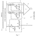
- a third embodiment of the present invention relates to a detection circuit for instantaneous voltage drop.
- the third embodiment is substantially the same as the first or second embodiment, and the main difference lies in that: in the third embodiment of the present invention, as shown in Fig. 7 , the determination unit 14 is further configured to receive an auxiliary detection signal W2 outputted by a system where the ignition device is located; and the determination unit 14 is configured to determine that the to-be-detected voltage VBATT drops instantaneously upon detection that the comparator 13 is inverted and the auxiliary detection signal W2 changes.
- the auxiliary detection signal W2 is a signal that changes before and after the ignition of the ignition device.
- the system where the ignition device is located is a vehicle system
- the auxiliary detection signal W2 may be, for example, a speed control signal of the vehicle.
- the magnitude of the voltage of the speed control signal does not match the magnitude of the voltage received by the determination unit 14, and thus in the example of Fig. 7 , the detection circuit further comprises a voltage conversion unit 17; and the determination unit 14 receives the auxiliary detection signal W2 by means of the voltage conversion unit 17.
- the determination unit 14 can directly receive the auxiliary detection signal W2.
- the specific type of the auxiliary detection signal W2 may be selected according to actual application scenarios.
- the voltage conversion unit 17 comprises a third resistor R5, a fourth resistor R6, an electronic switch VT3, a pull-up resistor R7, and a pull-up power source VCC.
- a first end of the third resistor R5 is used for receiving the auxiliary detection signal W2, a second end of the third resistor R5 is connected to a first end of the fourth resistor R6, and a second end of the fourth resistor R6 is grounded;
- a control end of the electronic switch VT3 is connected to the first end of the fourth resistor R6, a first conduction end of the electronic switch VT3 is connected to the pull-up power source VCC by means of the pull-up resistor R7 and is connected to the determination unit 14, and a second conduction end of the electronic switch VT3 is grounded.
- the electronic switch VT3 is, for example, a triode
- the control end, the first conduction end and the second conduction end of the electronic switch VT3 are respectively a base electrode, a collector electrode and an emitter electrode of the triode.
- the system does not output the auxiliary detection signal W2, and at this time, the electronic switch VT3 is in an off state, but due to the effect of the pull-up resistor R7, the first conduction end of the electronic switch VT3 outputs a high-level signal to the determination unit 14; and this high-level signal can be regarded as an auxiliary detection signal W2 before the ignition.
- the system outputs an auxiliary detection signal W2, and at this time, the electronic switch VT3 is turned on, and the first conduction end of the electronic switch VT3 outputs a low-level signal, and this low-level signal can be regarded as an auxiliary detection signal W2 after the ignition.
- the determination unit 14 can determine whether the auxiliary detection signal W2 changes from a high level to a low level upon detection that the comparator 13 is inverted; and if it is detected that the auxiliary detection signal W2 changes from a high level to a low level, it is determined that the to-be-detected voltage drops instantaneously; and if it is not detected that the auxiliary detection signal W2 changes from a high level to a low level, it is determined that the to-be-detected voltage does not drop instantaneously.
- auxiliary detection signal W2 changing from a high level to a low level represents a situation after the ignition, and it can be determined according to the specific type of the auxiliary detection signal W2 and the specific structure of the voltage conversion unit 17, as long as the auxiliary detection signal W2 changes.
- detection of the auxiliary detection signal W2 is added to assist in determining whether the to-be-detected voltage drops instantaneously, which can increase the detection accuracy, and avoid misjudgment caused by external factors.
- a fourth embodiment of the present invention relates to an on-board diagnostic system, comprising: the detection circuit for instantaneous voltage drop according to any one of the described embodiments.
- this embodiment is a system embodiment corresponding to any one of the first to third embodiments, and this embodiment may be implemented in cooperation with any one of the first to third embodiments.
- Related technical details mentioned in any one of the first to third embodiments are still valid in this embodiment, and will not be repeated herein again to reduce repetition. Accordingly, the related technical details mentioned in the present embodiment can also be applied to any one of the first to third embodiments.
Abstract
Description
- The present invention is proposed on the basis of
Chinese Patent Application No. 201910777986.6 and filed on August 22, 2019 - Embodiments of the present invention relate to the technical field of detection, and in particular, to a detection circuit for instantaneous voltage drop and an on-board diagnostic system.
- Regarding an on-board diagnostics (OBD for short) system, the system is used for monitoring the operating condition of an engine and the operating state of an exhaust post-treatment system at any time. Once it is found that an excessive emission situation possibly occurs, a warning is sent immediately. For example, the OBD can monitor, in real time, operating data such as whether a vehicle is ignited, whether the vehicle is speeding and whether the fuel consumption is excessively high, and can analyze whether a fault occurs. If the system fails, a fault light or an engine-checking warning light is turned on; and the OBD system stores the fault information in a memory, and related information may be read in the form of fault codes by means of a standard diagnostic instrument and diagnostic interface. According to prompt of the fault codes, a maintenance personnel can quickly and accurately determine the nature and position of the fault. The OBD ensures the safety of travel of the vehicle, and records conditions of the vehicle.
- Embodiments of the present invention provide a detection circuit for instantaneous voltage drop and an on-board diagnostic system.
- Embodiments of the present invention provide a detection circuit for instantaneous voltage drop, comprising: two RC circuits, a comparator and a determination unit; each RC circuit comprises a first resistor, a second resistor and an energy storage capacitor; a first end of the first resistor is configured to receive a to-be-detected voltage, a second end of the first resistor is connected to a first end of the second resistor, and a second end of the second resistor is grounded; the energy storage capacitor is connected in parallel with the second resistor; the first end of the second resistor forms an output end of the RC circuit; the output ends of the two RC circuits are correspondingly connected to two input ends of the comparator, respectively; an output end of the comparator is connected to the determination unit; wherein in the two RC circuits, resistance ratios of the second resistors to the first resistors are different, capacitances of the energy storage capacitors are different, and the capacitance of the energy storage capacitor in the RC circuit with a larger resistance ratio of the second resistor to the first resistor is smaller; and the determination unit is configured to determine that the to-be-detected voltage drops instantaneously when it is at least detected that the comparator is inverted.
- Embodiments of the present invention further provide an on-board diagnostic system, comprising: the described detection circuit for instantaneous voltage drop.
- Exemplary illustrations are made on one or more embodiments by means of figures in the accompanying drawings corresponding thereto, and these exemplary illustrations are not intended to constitute limitation on the embodiments. Elements having the same reference numerals in the drawings are designated as like elements, and unless otherwise specified, the figures in the drawings are not intended to constitute limiting.
-
Fig. 1 is a schematic diagram of a detection circuit for instantaneous voltage drop according to a first embodiment of the present invention; -
Fig. 2 is a schematic diagram of a modification structure of the detection circuit according to the first embodiment of the present invention; -
Fig. 3 is a schematic diagram illustrating change of voltages received by two input ends of a comparator according to one example of the first embodiment of the present invention; -
Fig. 4 is a schematic diagram illustrating change of voltages received by two input ends of the comparator according to another example of the first embodiment of the present invention; -
Fig. 5 is a schematic diagram of a circuit comprising a connector and an ESD and EMI protection circuit according to the first embodiment of the present invention; -
Fig. 6 is a schematic diagram of a detection circuit for instantaneous voltage drop according to a second embodiment of the present invention; and -
Fig. 7 is a schematic diagram of a detection circuit for instantaneous voltage drop according to a third embodiment of the present invention. - To make the objects, technical solutions, and advantages of the embodiments of the present invention clearer, hereinafter, embodiments of the present invention will be described in detail in combination with the accompanying drawings. However, a person of ordinary skill in the art may understand that in the embodiments of the present invention, many technical details are proposed to enable a reader to better understand some embodiments of the present invention. However, even without these technical details, based on various changes and modifications of the following embodiments, the technical solutions of some embodiments of the present invention can also be achieved. Dividing of the following embodiments is for convenience of description, and shall not constitute any limitation to specific implementations of some embodiments of the present invention. The embodiments may be referred to each other and combined with each other without any contradiction.
- A first embodiment of the present invention relates to a detection circuit for instantaneous voltage drop, which can be applied to voltage detection in any scenarios where a voltage may drop instantaneously; for example, when a vehicle is ignited, the voltage of a power source for supplying power to an ignition device will drop instantaneously, and therefore the circuit of some embodiments of the present invention can be used for detecting whether the vehicle is ignited. However, the scenarios are not limited in this embodiment. The detection circuit for instantaneous voltage drop in some embodiments of the present invention can be applied to any scenarios in which it is required to detect whether a voltage drops instantaneously.
- As shown in
Fig. 1 , the detection circuit for instantaneous voltage drop comprises: two RC circuits, acomparator 13 and adetermination unit 14, the two RC circuits being respectively denoted as afirst RC circuit 11 and asecond RC circuit 12. Each RC circuit comprises a first resistor, a second resistor and an energy storage capacitor. For ease of description, in this embodiment, the first resistors in the two RC circuits are respectively denoted by reference signs R1 and R2, and hereinafter are respectively referred to as a resistor R1 and a resistor R2 for short; the second resistors in the two RC circuits are respectively denoted by reference signs R3 and R4, and hereinafter are respectively referred to as a resistor R3 and a resistor R4 for short; and the energy storage capacitors in the two RC circuits are respectively denoted by reference signs C1 and C2, and hereinafter are respectively referred to as a capacitor C1 and a capacitor C2 for short. - Specifically, in the
first RC circuit 11, a first end of the resistor R1 is used for receiving a to-be-detected voltage VBATT, a second end of the resistor R1 is connected to a first end of the resistor R3, and a second end of the resistor R3 is grounded; the capacitor C1 is connected in parallel with the resistor R3; and a first end of the resistor R3 forms an output end OUT1 of thefirst RC circuit 11. In thesecond RC circuit 12, a first end of the resistor R2 is used for receiving the to-be-detected voltage VBATT, a second end of the resistor R2 is connected to a first end of the resistor R4, and a second end of the resistor R4 is grounded; the capacitor C2 is connected in parallel with the resistor R4; and a first end of the resistor R4 forms an output end OUT2 of thesecond RC circuit 12. Output ends OUT1 and OUT2 of the two RC circuits are correspondingly connected to two input ends of thecomparator 13 respectively, and an output end of thecomparator 13 is connected to thedetermination unit 14. - In the present embodiment, the resistance ratios of the second resistors to the first resistors in the two RC circuits are different, which means that the resistance ratio of the resistor R3 to the resistor R1 in the
first RC circuit 11 is different from the resistance ratio of the resistor R4 to the resistor R2 in thesecond RC circuit 12. In thefirst RC circuit 11, both the resistor R1 and the resistor R3 have a voltage division function, and the voltage outputted by the output end OUT1 is the voltage across two ends of the resistor R3; and by the same reasoning, in thesecond RC circuit 12, the voltage outputted by the output end OUT2 is the voltage across two ends of the resistor R4. The to-be-detected voltage VBATT is inputted to both the first end of the resistor R1 and the first end of the resistor R2, that is, input voltages of thefirst RC circuit 11 and thesecond RC circuit 12 are the same. The resistance ratio of the resistor R3 to the resistor R1 is different from the resistance ratio of the resistor R4 to the resistor R2, which indicates that when the input voltages of thefirst RC circuit 11 and thesecond RC circuit 12 are the same, the voltage allocated to the resistor R3 in thefirst RC circuit 11 is different from the voltage allocated to the resistor R4 in thesecond RC circuit 12. Therefore, voltages received by the two input ends of thecomparator 13 are also different. - In the present embodiment , the capacitances of the energy storage capacitors in the two RC circuits are different, which means that the capacitance of the capacitor C1 in the
first RC circuit 11 is different from the capacitance of the capacitor C2 in thesecond RC circuit 12. Therefore, an RC discharge curve of thefirst RC circuit 11 is different from an RC discharge curve of thesecond RC circuit 12, that is, during discharging, the RC circuit with a larger capacitor capacitance discharges faster. - In the present embodiment , the capacitance of the energy storage capacitor in the RC circuit with a larger resistance ratio of the second resistor to the first resistor is less, which means that if the resistance ratio of the resistor R3 to the resistor R1 in the
first RC circuit 11 is greater than the resistance ratio of the resistor R4 to the resistor R2 in thesecond RC circuit 12, the capacitance of the energy storage capacitor in thefirst RC circuit 11 is less than the capacitance of the energy storage capacitor in thesecond RC circuit 12; and if the resistance ratio of the resistor R3 to the resistor R1 in thefirst RC circuit 11 is less than the resistance ratio of the resistor R4 to the resistor R2 in thesecond RC circuit 12, the capacitance of the energy storage capacitor in thefirst RC circuit 11 is greater than the capacitance of the energy storage capacitor in thesecond RC circuit 12. - The
determination unit 14 is configured to determine that the to-be-detected voltage drops instantaneously upon detection that thecomparator 13 is inverted. In this embodiment, thedetermination unit 14 may be a processing chip, for example, a main control chip of the on-board diagnostic system where the ignition device is located. However, the present invention is not limited thereto, and thedetermination unit 14 may also be implemented by a hardware circuit. - As shown in the example of
Fig. 1 , the output end OUT1 of thefirst RC circuit 11 is connected to a non-inverting input end of thecomparator 13, and the output end OUT2 of thesecond RC circuit 12 is connected to an inverting input end of thecomparator 13; and the resistance ratio of the resistor R3 to the resistor R1 is less than the resistance ratio of the resistor R4 to the resistor R2, and the capacitance of the capacitor C1 is greater than the capacitance of the capacitor C2. - In an example, in order to facilitate the selection of resistors and capacitors in production and manufacturing, as shown in
Fig. 2 , the capacitor C1 may be designed as a first sub-capacitor C1_1 and a second sub-capacitor C1_2 connected in parallel, wherein the capacitance of the first sub-capacitor C1-1 is the same as the capacitance of the capacitor C2, so as to satisfy that the capacitance of the capacitor C1 is greater than the capacitance of the capacitor C2. Moreover, the resistor R3 and the resistor R4 may be set as two resistors having the same resistance value, and the resistance value of the resistor R1 is greater than the resistance value of the resistor R2, so as to satisfy that the resistance ratio of the resistor R3 to the resistor R1 is less than the resistance ratio of the resistor R4 to the resistor R2. Values of various resistors and capacitors can be for example, R1 = 100 ohms, R2 = 90 ohms, R3 = R4 = 30 ohms, C1_1 = C2 = 0.1 microfarads, and C1_2 = 10 microfarads; wherein the capacitance of the capacitor C1_2 may be much greater than the capacitance of the capacitor C1_1, so that the drop speed of the voltage outputted by the output end OUT1 is greatly decreased relative to the drop speed of the voltage outputted by the output end OUT2. - Hereinafter, the operation principle of the detection circuit in
Fig. 1 is described in detail. - The resistance ratio of the resistor R3 to the resistor R1 is less than the resistance ratio of the resistor R4 and the resistor R2, and input voltages of the
first RC circuit 11 and thesecond RC circuit 12 are both the to-be-detected voltage VBATT, and thus the voltage allocated to the resistor R3 in thefirst RC circuit 11 is less than the voltage allocated to the resistor R4 in thesecond RC circuit 12. The voltage V+ received by the non-inverting input end of thecomparator 13 is the voltage outputted by the output end OUT1, and the voltage V- received by the inverting input end of the comparator is the voltage outputted by the output end OUT2, and thus when the vehicle is not ignited, that is, when the to-be-detected voltage VBATT is in a steady state, the voltage V+ received by the non-inverting input end of thecomparator 13 is less than the voltage V- received by the inverting input end, and thus an output voltage W1 of an output end of thecomparator 13 is a low-level signal, as shown inFig. 3 . - When the vehicle is ignited, that is, time T0 in
Fig. 3 , the to-be-detected voltage VBATT instantaneously drops, the voltage across both ends of the resistor R3 and the voltage across both ends of the resistor R4 drop quickly, but due to the effect of discharging of capacitors connected in parallel with the resistors, the drop speed of the voltage across both ends of the resistor R3 and the drop speed of the voltage across both ends of the resistor R4 will slow down. The capacitance of the capacitor C1 is greater than the capacitance of the capacitor C2, and thus before the vehicle is ignited, the quantity of electric charge stored in the capacitor C1 is greater than the quantity of electric charge stored in the capacitor C2, and the discharge duration of the capacitor C1 is longer than the discharge duration of the capacitor C2. Therefore, the drop speed of the voltage across two ends of the resistor R3 is slower than the drop speed of the voltage across two ends of the resistor R4, and the drop speed of the voltage V+ received by the non-inverting input end of thecomparator 13 is less than the drop speed of the voltage V- received by the inverting input end, so that starting from time T1 as shown inFig. 3 , the voltage V+ received by the non-inverting input end of thecomparator 13 is greater than the voltage V- received by the inverting input end, and at this time, the output voltage W1 of the output end OUT of thecomparator 13 is a high-level signal, that is, thecomparator 13 is inverted. Upon detection that thecomparator 13 is inverted, thedetermination unit 14 can determine that the to-be-detected voltage VBATT drops instantaneously, that is, the vehicle is ignited. - After the ignition is completed, the voltage of a power supply source of the ignition device will increase, that is, the to-be-detected voltage VBATT will increase back to a steady state, and therefore the voltages outputted by the output end OUT1 and the output end OUT2 will also slowly increase and tend to a steady state, and the voltage (i.e., the voltage V+ received by the non-inverting input end of the comparator 13) outputted by the output end OUT1 will be less than the voltage(i.e., the voltage V- received by the inverting input end of the comparator 13) outputted by the output end OUT2 again. As shown by time T2 in
Fig. 3 , this time represents a time at which the voltage V+ recovers to be less than the voltage V-, and at this time, the output voltage W1 of the output end of thecomparator 13 is a low-level signal. - In another example, the output end OUT1 of the
first RC circuit 11 is connected to the inverting input end of thecomparator 13, the output end OUT1 of thesecond RC circuit 12 is connected to the non-inverting input end of thecomparator 13, and all the resistance values of the resistors and the capacitances of the capacitors are the same as those in the example inFig. 3 , and then the implementation principle thereof is substantially the same as that of the example inFig. 3 , and the difference merely lies in that: as shown inFig. 4 , when the vehicle is not ignited, that is, the to-be-detected voltage VBATT is in a steady state, the voltage V-received by the inverting input end of thecomparator 13 is less than the voltage V+ received by the non-inverting input end of thecomparator 13, and thus the output voltage W1 of the output end of thecomparator 13 is a high-level signal; and in the T1 - T2 time period after the ignition of the vehicle, the voltage V- received by the inverting input end of thecomparator 13 is greater than the voltage V+ received by the non-inverting input end of thecomparator 13, and the output voltage W1 of the output end of thecomparator 13 is a low-level signal, that is, the comparator is inverted. Upon detection that thecomparator 13 is inverted, thedetermination unit 14 can determine that the to-be-detected voltage VBATT drops instantaneously, that is, the vehicle is ignited. After the ignition is completed, the to-be-detected voltage VBATT increases to a steady state, that is, after the time T2, the output voltage W1 of the output end of thecomparator 13 is a high-level signal. - In this embodiment, the resistance ratios of the second resistors to the first resistors in the two RC circuits are different, and thus after voltage division, the magnitudes of the voltages inputted to the two input ends of the comparator are different, and their relative magnitude remains unchanged in the steady state; wherein the voltage inputted, to the comparator, by the RC circuit with a larger resistance ratio of the second resistor to the first resistor is larger. The capacitances of the energy storage capacitors in the two RC circuits are different, such that the discharge durations of the energy storage capacitors in the two RC circuits are different. Furthermore, the capacitance of the energy storage capacitor in the RC circuit with a larger resistance ratio of the second resistor to the first resistor is smaller, and thus when the to-be-detected voltage drops instantaneously, the discharge duration of the RC circuit inputting a larger voltage to the comparator is shorter, while the discharge duration of the RC circuit inputting a smaller voltage to the comparator is longer, such that at a certain time after the to-be-detected voltage drops instantaneously, the relative magnitude of the voltages inputted to the two input ends of the comparator changes, and thus the comparator is inverted. Therefore, whether the to-be-detected voltage drops instantaneously can be determined on the basis whether the comparator is inverted. Furthermore, the detection circuit in some embodiments of the present invention has a simple structure, a small layout, low cost and a high detection speed.
- In detecting whether ignition occurs, upon detection that the comparator is inverted, it can be determined that the to-be-detected voltage drops instantaneously, that is, as shown in time T1 in
Figs.3 and4 , it can be detected that the comparator is inverted. However, regarding the solution in the prior art in which battery voltages at different times are detected and it is determined that ignition occurs upon detection that the battery voltage at a later time is higher than the battery voltage at a previous time, because in the prior art, detecting that the battery voltage at a later time is higher refers to a time when the battery voltage will increase again after the ignition, that is, after the time T2 shown inFigs. 3 and4 , while in some embodiments of the present invention, it can be determined that the comparator is inverted necessarily before the battery voltage increases again after the ignition, with respect to the prior art, in some embodiments of the present invention, whether ignition occurs can be detected more timely, having better timeliness. - In addition, the circuit in this embodiment can further comprise a
connector 15. As shown inFig. 5 , theconnector 15 is configured to acquire the to-be-detected voltage VBATT from a power source and input the to-be-detected voltage VBATT into the two RC circuits. When the circuit according to this embodiment is used for detecting whether a vehicle is ignited, the to-be-detected voltage VBATT needs to be acquired from the power supply source of the ignition device, and theconnector 15 is, for example, an OBD interface of the vehicle. The type of theconnector 15 needs to be set. In addition, the circuit in this embodiment can further comprise an ESD (electrostatic) and EMI (electromagnetic)protection circuit 16, provided between theconnector 15 and the RC circuits, and functioning to isolate electrostatic and electromagnetic interferences. - A second embodiment of the present invention relates to a detection circuit for instantaneous voltage drop. The second embodiment is substantially the same as the first embodiment, and the main difference lies in that: in the second embodiment of the present invention, as shown in
Fig. 6 , the detection circuit further comprises two diodes VT1 and VT2, and the first ends of the first resistors in the two RC circuits are correspondingly connected to the two diodes respectively, so as to receive the to-be-detected voltage by means of the diodes. - Specifically, a first end of the
resistor 1 in thefirst RC circuit 11 is connected to a cathode of the diode VT1, and a first end of the resistor 2 in thesecond RC circuit 12 is connected to a cathode of the diode VT2; and anodes of the diodes VT1 and VT2 are both connected to the ESD andEMI protection circuit 16 inFig. 6 . It should be noted thatFig. 6 is an improvement based onFig. 5 , but it is not limited thereto.Fig. 6 may also be an improvement based onFig. 1 or Fig. 2 , that is, In the case that theconnector 15 and the ESD andEMI protection circuit 16 do not need to be provided, anodes of the diodes VT1 and VT2 may be directly connected to a positive electrode of the power source so as to acquire the to-be-detected voltage VBATT. - In this embodiment, the diodes additionally provided between the RC circuits and a battery power source which outputs the to-be-detected voltage VBATT not only can prevent a rear-end current from flowing backward and damaging the battery power source, but also can prevent the detection circuit in some embodiments of the present invention from being damaged due to a wiring error between the battery power source and the detection circuit, thereby greatly improving the product safety. The wiring error is, for example, connecting a negative electrode of the power source to the first end of the resistor R1 and the first end of the resistor R2 in the RC circuits.
- A third embodiment of the present invention relates to a detection circuit for instantaneous voltage drop. The third embodiment is substantially the same as the first or second embodiment, and the main difference lies in that: in the third embodiment of the present invention, as shown in
Fig. 7 , thedetermination unit 14 is further configured to receive an auxiliary detection signal W2 outputted by a system where the ignition device is located; and thedetermination unit 14 is configured to determine that the to-be-detected voltage VBATT drops instantaneously upon detection that thecomparator 13 is inverted and the auxiliary detection signal W2 changes. The auxiliary detection signal W2 is a signal that changes before and after the ignition of the ignition device. - In this embodiment, the system where the ignition device is located is a vehicle system, and the auxiliary detection signal W2 may be, for example, a speed control signal of the vehicle. The magnitude of the voltage of the speed control signal does not match the magnitude of the voltage received by the
determination unit 14, and thus in the example ofFig. 7 , the detection circuit further comprises avoltage conversion unit 17; and thedetermination unit 14 receives the auxiliary detection signal W2 by means of thevoltage conversion unit 17. However, it is not limited thereto, in other examples, if the selected auxiliary detection signal W2 matches the magnitude of the voltage of thedetermination unit 14, thedetermination unit 14 can directly receive the auxiliary detection signal W2. Furthermore, in other examples, the specific type of the auxiliary detection signal W2 may be selected according to actual application scenarios. - In one example, as shown in
Fig. 7 , thevoltage conversion unit 17 comprises a third resistor R5, a fourth resistor R6, an electronic switch VT3, a pull-up resistor R7, and a pull-up power source VCC. Specifically, a first end of the third resistor R5 is used for receiving the auxiliary detection signal W2, a second end of the third resistor R5 is connected to a first end of the fourth resistor R6, and a second end of the fourth resistor R6 is grounded; a control end of the electronic switch VT3 is connected to the first end of the fourth resistor R6, a first conduction end of the electronic switch VT3 is connected to the pull-up power source VCC by means of the pull-up resistor R7 and is connected to thedetermination unit 14, and a second conduction end of the electronic switch VT3 is grounded. In this embodiment, the electronic switch VT3 is, for example, a triode, and the control end, the first conduction end and the second conduction end of the electronic switch VT3 are respectively a base electrode, a collector electrode and an emitter electrode of the triode. - In the case that the ignition is not performed, the system does not output the auxiliary detection signal W2, and at this time, the electronic switch VT3 is in an off state, but due to the effect of the pull-up resistor R7, the first conduction end of the electronic switch VT3 outputs a high-level signal to the
determination unit 14; and this high-level signal can be regarded as an auxiliary detection signal W2 before the ignition. After the ignition, the system outputs an auxiliary detection signal W2, and at this time, the electronic switch VT3 is turned on, and the first conduction end of the electronic switch VT3 outputs a low-level signal, and this low-level signal can be regarded as an auxiliary detection signal W2 after the ignition. - Therefore, the
determination unit 14 can determine whether the auxiliary detection signal W2 changes from a high level to a low level upon detection that thecomparator 13 is inverted; and if it is detected that the auxiliary detection signal W2 changes from a high level to a low level, it is determined that the to-be-detected voltage drops instantaneously; and if it is not detected that the auxiliary detection signal W2 changes from a high level to a low level, it is determined that the to-be-detected voltage does not drop instantaneously. It should be noted that in other examples, it is not limited that the auxiliary detection signal W2 changing from a high level to a low level represents a situation after the ignition, and it can be determined according to the specific type of the auxiliary detection signal W2 and the specific structure of thevoltage conversion unit 17, as long as the auxiliary detection signal W2 changes. - In this embodiment, detection of the auxiliary detection signal W2 is added to assist in determining whether the to-be-detected voltage drops instantaneously, which can increase the detection accuracy, and avoid misjudgment caused by external factors.
- A fourth embodiment of the present invention relates to an on-board diagnostic system, comprising: the detection circuit for instantaneous voltage drop according to any one of the described embodiments.
- It is easily found that this embodiment is a system embodiment corresponding to any one of the first to third embodiments, and this embodiment may be implemented in cooperation with any one of the first to third embodiments. Related technical details mentioned in any one of the first to third embodiments are still valid in this embodiment, and will not be repeated herein again to reduce repetition. Accordingly, the related technical details mentioned in the present embodiment can also be applied to any one of the first to third embodiments.
Claims (10)
- A detection circuit for instantaneous voltage drop, comprising: two RC circuits, a comparator and a determination unit;each RC circuit comprises a first resistor, a second resistor and an energy storage capacitor; a first end of the first resistor is used for receiving a to-be-detected voltage, a second end of the first resistor is connected to a first end of the second resistor, and a second end of the second resistor is grounded; the energy storage capacitor is connected in parallel with the second resistor; the first end of the second resistor forms an output end of the RC circuit;output ends of the two RC circuits are correspondingly connected to two input ends of the comparator respectively; an output end of the comparator is connected to the determination unit;wherein in the two RC circuits, resistance ratios of the second resistors to the first resistors are different, capacitances of the energy storage capacitors are different, and the capacitance of the energy storage capacitor in the RC circuit with a larger resistance ratio of the second resistor to the first resistor is smaller; and the determination unit is configured to determine that the to-be-detected voltage drops instantaneously when it is at least detected that the comparator is inverted.
- The detection circuit for instantaneous voltage drop according to claim 1, wherein the to-be-detected voltage is a voltage outputted by a battery power source supplying power to an ignition device;
wherein when the ignition device is ignited, the to-be-detected voltage drops instantaneously. - The detection circuit for instantaneous voltage drop according to claim 2, wherein the determination unit is further configured to receive an auxiliary detection signal outputted by a system where the ignition device is located; the auxiliary detection signal is a signal which changes before and after ignition of the ignition device;
wherein the determination unit is configured to determine that the to-be-detected voltage drops instantaneously upon detection that the comparator is inverted and the auxiliary detection signal changes. - The detection circuit for instantaneous voltage drop according to claim 1, wherein the detection circuit further comprises two diodes, and the first ends of the first resistors in the two RC circuits are correspondingly connected to the two diodes respectively, so as to receive the to-be-detected voltage by means of the diodes.
- The detection circuit for instantaneous voltage drop according to claim 1, wherein the two RC circuits are respectively denoted as a first RC circuit and a second RC circuit;
the energy storage capacitor in the first RC circuit comprises a first sub-capacitor and a second sub-capacitor which are connected in parallel, and the capacitance of the first sub-capacitor is equal to the capacitance of the energy storage capacitor in the second RC circuit; and a resistance value of the second resistor in the first RC circuit is equal to a resistance value of the second resistor in the second RC circuit, and a resistance value of the first resistor in the first RC circuit is greater than a resistance value of the first resistor in the second RC circuit. - The detection circuit for instantaneous voltage drop according to claim 3, wherein the detection circuit further comprises a voltage conversion unit; and
the determination unit receives the auxiliary detection signal by means of the voltage conversion unit. - The detection circuit for instantaneous voltage drop according to claim 6, wherein the voltage conversion unit comprises: a third resistor, a fourth resistor, an electronic switch, a pull-up resistor, and a pull-up power source;
a first end of the third resistor is used for receiving the auxiliary detection signal, a second end of the third resistor is connected to a first end of the fourth resistor, and a second end of the fourth resistor is grounded; and a control end of the electronic switch is connected to the first end of the fourth resistor, a first conduction end of the electronic switch is connected to the pull-up power source by means of the pull-up resistor and is connected to the determination unit, and a second conduction end of the electronic switch is grounded. - The detection circuit for instantaneous voltage drop according to claim 7, wherein the electronic switch is a triode.
- The detection circuit for instantaneous voltage drop according to claim 1, wherein the determination unit is a main control chip of a system where the ignition device is located.
- An on-board diagnostic system, comprising: the detection circuit for instantaneous voltage drop as claimed in any one of claims 1 to 9.
Applications Claiming Priority (2)
| Application Number | Priority Date | Filing Date | Title |
|---|---|---|---|
| CN201910777986.6A CN112415294A (en) | 2019-08-22 | 2019-08-22 | Detection circuit for instantaneous voltage drop and vehicle-mounted diagnosis system |
| PCT/CN2020/084508 WO2021031584A1 (en) | 2019-08-22 | 2020-04-13 | Detection circuit for instantaneous voltage drop and vehicle-mounted diagnostic system |
Publications (3)
| Publication Number | Publication Date |
|---|---|
| EP4019985A1 true EP4019985A1 (en) | 2022-06-29 |
| EP4019985A4 EP4019985A4 (en) | 2022-11-02 |
| EP4019985B1 EP4019985B1 (en) | 2023-09-13 |
Family
ID=74659634
Family Applications (1)
| Application Number | Title | Priority Date | Filing Date |
|---|---|---|---|
| EP20855013.7A Active EP4019985B1 (en) | 2019-08-22 | 2020-04-13 | Detection circuit for instantaneous voltage drop and vehicle-mounted diagnostic system |
Country Status (6)
| Country | Link |
|---|---|
| US (1) | US11926271B2 (en) |
| EP (1) | EP4019985B1 (en) |
| JP (1) | JP7462686B2 (en) |
| KR (1) | KR20220050094A (en) |
| CN (1) | CN112415294A (en) |
| WO (1) | WO2021031584A1 (en) |
Family Cites Families (24)
| Publication number | Priority date | Publication date | Assignee | Title |
|---|---|---|---|---|
| US4260907A (en) | 1979-06-12 | 1981-04-07 | Telex Computer Products, Inc. | Power-on-reset circuit with power fail detection |
| JPS6245396A (en) * | 1985-08-21 | 1987-02-27 | Mitsubishi Heavy Ind Ltd | Method of making drinking water using carbon dioxide |
| FR2586482B1 (en) * | 1985-08-23 | 1988-02-19 | Abiven Jacques | DEVICE FOR MONITORING A BATTERY |
| JPS63137527U (en) * | 1987-02-23 | 1988-09-09 | ||
| JP2731528B2 (en) * | 1987-12-28 | 1998-03-25 | 日本電気株式会社 | DC power supply instantaneous interruption detection device |
| JPH047448A (en) | 1990-04-24 | 1992-01-10 | Sanko Metal Ind Co Ltd | Wall panel and wall body |
| JPH06245396A (en) * | 1993-02-18 | 1994-09-02 | Fujitsu Ten Ltd | Voltage drop detector for vehicle battery power source |
| JPH0677448U (en) * | 1993-04-12 | 1994-10-28 | 怡利電子工業股▲ひん▼有限公司 | Battery saturation charge detection circuit |
| US5570258A (en) | 1995-05-11 | 1996-10-29 | Texas Instruments Incorporated | Phase monitor and protection apparatus |
| US6166547A (en) | 2000-03-14 | 2000-12-26 | Ag Communication Systems Corporation | Line card loss of battery detector |
| US6747470B2 (en) | 2001-12-19 | 2004-06-08 | Intel Corporation | Method and apparatus for on-die voltage fluctuation detection |
| JP4404851B2 (en) | 2003-06-05 | 2010-01-27 | 三菱電機株式会社 | Instantaneous voltage drop detection device |
| JP4820061B2 (en) * | 2004-03-05 | 2011-11-24 | 日立工機株式会社 | Battery tools |
| US6995605B2 (en) | 2004-03-31 | 2006-02-07 | Intel Corporation | Resonance suppression circuit |
| US7467050B2 (en) * | 2006-05-30 | 2008-12-16 | International Business Machines Corporation | Method for detecting noise events in systems with time variable operating points |
| JP2008268084A (en) | 2007-04-23 | 2008-11-06 | Denso Corp | Removable distribution system short-circuit fault detection device |
| US7720621B2 (en) | 2007-08-30 | 2010-05-18 | International Business Machines Corporation | Application of multiple voltage droop detection |
| CN101290332B (en) | 2008-05-14 | 2010-10-13 | 深圳创维-Rgb电子有限公司 | Voltage up-down detection circuit and method |
| US8498172B1 (en) * | 2010-08-31 | 2013-07-30 | Western Digital Technologies, Inc. | Data storage device evaluating frequency range of supply voltage to detect power failure |
| US8917070B2 (en) * | 2013-03-14 | 2014-12-23 | Vidatronic, Inc. | LDO and load switch supporting a wide range of load capacitance |
| CN106499561B (en) | 2015-09-06 | 2018-09-04 | 北京握奇智能科技有限公司 | A kind of device and method of determining automobile engine start and stop state |
| EP3907849A1 (en) * | 2017-08-25 | 2021-11-10 | Guangdong Oppo Mobile Telecommunications Corp., Ltd. | Terminal device, battery system, and device for detecting battery abnormality |
| US10205375B1 (en) | 2017-09-15 | 2019-02-12 | Oracle International Corporation | Automated power supply sense line selection |
| CN207504562U (en) | 2017-12-06 | 2018-06-15 | 广东工业大学 | A kind of protection circuit against input over-voltage for having the function of to power on Inrush current restraining |
-
2019
- 2019-08-22 CN CN201910777986.6A patent/CN112415294A/en active Pending
-
2020
- 2020-04-13 EP EP20855013.7A patent/EP4019985B1/en active Active
- 2020-04-13 US US17/624,432 patent/US11926271B2/en active Active
- 2020-04-13 KR KR1020217042795A patent/KR20220050094A/en unknown
- 2020-04-13 JP JP2021577536A patent/JP7462686B2/en active Active
- 2020-04-13 WO PCT/CN2020/084508 patent/WO2021031584A1/en unknown
Also Published As
| Publication number | Publication date |
|---|---|
| US11926271B2 (en) | 2024-03-12 |
| US20220363208A1 (en) | 2022-11-17 |
| EP4019985A4 (en) | 2022-11-02 |
| WO2021031584A1 (en) | 2021-02-25 |
| KR20220050094A (en) | 2022-04-22 |
| CN112415294A (en) | 2021-02-26 |
| JP2022544898A (en) | 2022-10-24 |
| JP7462686B2 (en) | 2024-04-05 |
| EP4019985B1 (en) | 2023-09-13 |
Similar Documents
| Publication | Publication Date | Title |
|---|---|---|
| EP1930737B1 (en) | Insulating resistance detection apparatus | |
| CN110774907B (en) | Detection and single wake-up circuit for charging CC signal | |
| US11899076B2 (en) | Device for automatic detection of coupling between electronic devices | |
| CN101565027A (en) | High-voltage bus discharge with logarithmic self-protection | |
| CN110636664B (en) | Indicator lamp driving circuit with diagnosis function | |
| CN101072939B (en) | Electrical circuit for controlling a piezoelectric element, particularly of a fuel injection system of a motor vehicle | |
| EP2637276A1 (en) | Protection circuit for lithium-ion battery | |
| US10836338B2 (en) | Method and device for monitoring an energy reserve and safety device for a vehicle | |
| US11708801B2 (en) | Load drive device, engine system | |
| JP2014098681A (en) | Electric leakage detector | |
| JP6930745B2 (en) | Management equipment and power supply system | |
| KR20160144484A (en) | Method and device for ascertaining an inner resistance of a supply network for supplying energy to a personal protection device of a vehicle | |
| EP4019985A1 (en) | Detection circuit for instantaneous voltage drop and vehicle-mounted diagnostic system | |
| JP2880058B2 (en) | Misfire detection device for internal combustion engine | |
| CN112213573B (en) | High-voltage interlocking loop detection method and circuit | |
| CN210222174U (en) | Carrier rocket initiating explosive device path test circuit | |
| CN104111399A (en) | Vehicle electronic control unit ground connection and ground pressure difference detection circuit | |
| CN100395555C (en) | Latching effect detecting method for CMOS circuit | |
| JP4188788B2 (en) | Capacity discharge ignition device | |
| CN216816805U (en) | Wake-up circuit, detection circuit, control guide circuit, chip and vehicle | |
| US4689554A (en) | Test apparatus for electronic control systems, particularly automotive-type computers | |
| CN103287357B (en) | Controller of vehicle, vehicle control system and control method for vehicle | |
| CN112461114A (en) | Detection device of inductive sensor, automobile and automobile body height detection method of automobile | |
| CN220711163U (en) | Discharge loop of energy storage capacitor, safety airbag control unit and electric automobile | |
| CN111313373B (en) | Power supply circuit, circuit fault detection method, circuit board and vehicle-mounted air conditioner |
Legal Events
| Date | Code | Title | Description |
|---|---|---|---|
| STAA | Information on the status of an ep patent application or granted ep patent |
Free format text: STATUS: THE INTERNATIONAL PUBLICATION HAS BEEN MADE |
|
| PUAI | Public reference made under article 153(3) epc to a published international application that has entered the european phase |
Free format text: ORIGINAL CODE: 0009012 |
|
| STAA | Information on the status of an ep patent application or granted ep patent |
Free format text: STATUS: REQUEST FOR EXAMINATION WAS MADE |
|
| 17P | Request for examination filed |
Effective date: 20211228 |
|
| AK | Designated contracting states |
Kind code of ref document: A1 Designated state(s): AL AT BE BG CH CY CZ DE DK EE ES FI FR GB GR HR HU IE IS IT LI LT LU LV MC MK MT NL NO PL PT RO RS SE SI SK SM TR |
|
| A4 | Supplementary search report drawn up and despatched |
Effective date: 20221004 |
|
| RIC1 | Information provided on ipc code assigned before grant |
Ipc: G01R 19/00 20060101ALI20220927BHEP Ipc: G01R 17/02 20060101ALI20220927BHEP Ipc: G01R 31/00 20060101ALI20220927BHEP Ipc: G01R 19/165 20060101AFI20220927BHEP |
|
| DAV | Request for validation of the european patent (deleted) | ||
| DAX | Request for extension of the european patent (deleted) | ||
| GRAP | Despatch of communication of intention to grant a patent |
Free format text: ORIGINAL CODE: EPIDOSNIGR1 |
|
| STAA | Information on the status of an ep patent application or granted ep patent |
Free format text: STATUS: GRANT OF PATENT IS INTENDED |
|
| RIC1 | Information provided on ipc code assigned before grant |
Ipc: G01R 19/00 20060101ALI20230314BHEP Ipc: G01R 17/02 20060101ALI20230314BHEP Ipc: G01R 31/00 20060101ALI20230314BHEP Ipc: G01R 19/165 20060101AFI20230314BHEP |
|
| INTG | Intention to grant announced |
Effective date: 20230411 |
|
| GRAS | Grant fee paid |
Free format text: ORIGINAL CODE: EPIDOSNIGR3 |
|
| GRAA | (expected) grant |
Free format text: ORIGINAL CODE: 0009210 |
|
| STAA | Information on the status of an ep patent application or granted ep patent |
Free format text: STATUS: THE PATENT HAS BEEN GRANTED |
|
| AK | Designated contracting states |
Kind code of ref document: B1 Designated state(s): AL AT BE BG CH CY CZ DE DK EE ES FI FR GB GR HR HU IE IS IT LI LT LU LV MC MK MT NL NO PL PT RO RS SE SI SK SM TR |
|
| REG | Reference to a national code |
Ref country code: CH Ref legal event code: EP |
|
| REG | Reference to a national code |
Ref country code: DE Ref legal event code: R096 Ref document number: 602020017796 Country of ref document: DE |
|
| REG | Reference to a national code |
Ref country code: IE Ref legal event code: FG4D |
|
| REG | Reference to a national code |
Ref country code: LT Ref legal event code: MG9D |
|
| REG | Reference to a national code |
Ref country code: NL Ref legal event code: MP Effective date: 20230913 |
|
| PG25 | Lapsed in a contracting state [announced via postgrant information from national office to epo] |
Ref country code: GR Free format text: LAPSE BECAUSE OF FAILURE TO SUBMIT A TRANSLATION OF THE DESCRIPTION OR TO PAY THE FEE WITHIN THE PRESCRIBED TIME-LIMIT Effective date: 20231214 |
|
| PG25 | Lapsed in a contracting state [announced via postgrant information from national office to epo] |
Ref country code: SE Free format text: LAPSE BECAUSE OF FAILURE TO SUBMIT A TRANSLATION OF THE DESCRIPTION OR TO PAY THE FEE WITHIN THE PRESCRIBED TIME-LIMIT Effective date: 20230913 Ref country code: RS Free format text: LAPSE BECAUSE OF FAILURE TO SUBMIT A TRANSLATION OF THE DESCRIPTION OR TO PAY THE FEE WITHIN THE PRESCRIBED TIME-LIMIT Effective date: 20230913 Ref country code: NO Free format text: LAPSE BECAUSE OF FAILURE TO SUBMIT A TRANSLATION OF THE DESCRIPTION OR TO PAY THE FEE WITHIN THE PRESCRIBED TIME-LIMIT Effective date: 20231213 Ref country code: LV Free format text: LAPSE BECAUSE OF FAILURE TO SUBMIT A TRANSLATION OF THE DESCRIPTION OR TO PAY THE FEE WITHIN THE PRESCRIBED TIME-LIMIT Effective date: 20230913 Ref country code: LT Free format text: LAPSE BECAUSE OF FAILURE TO SUBMIT A TRANSLATION OF THE DESCRIPTION OR TO PAY THE FEE WITHIN THE PRESCRIBED TIME-LIMIT Effective date: 20230913 Ref country code: HR Free format text: LAPSE BECAUSE OF FAILURE TO SUBMIT A TRANSLATION OF THE DESCRIPTION OR TO PAY THE FEE WITHIN THE PRESCRIBED TIME-LIMIT Effective date: 20230913 Ref country code: GR Free format text: LAPSE BECAUSE OF FAILURE TO SUBMIT A TRANSLATION OF THE DESCRIPTION OR TO PAY THE FEE WITHIN THE PRESCRIBED TIME-LIMIT Effective date: 20231214 Ref country code: FI Free format text: LAPSE BECAUSE OF FAILURE TO SUBMIT A TRANSLATION OF THE DESCRIPTION OR TO PAY THE FEE WITHIN THE PRESCRIBED TIME-LIMIT Effective date: 20230913 |
|
| REG | Reference to a national code |
Ref country code: AT Ref legal event code: MK05 Ref document number: 1611796 Country of ref document: AT Kind code of ref document: T Effective date: 20230913 |
|
| PG25 | Lapsed in a contracting state [announced via postgrant information from national office to epo] |
Ref country code: NL Free format text: LAPSE BECAUSE OF FAILURE TO SUBMIT A TRANSLATION OF THE DESCRIPTION OR TO PAY THE FEE WITHIN THE PRESCRIBED TIME-LIMIT Effective date: 20230913 |
|
| PG25 | Lapsed in a contracting state [announced via postgrant information from national office to epo] |
Ref country code: IS Free format text: LAPSE BECAUSE OF FAILURE TO SUBMIT A TRANSLATION OF THE DESCRIPTION OR TO PAY THE FEE WITHIN THE PRESCRIBED TIME-LIMIT Effective date: 20240113 |
|
| PG25 | Lapsed in a contracting state [announced via postgrant information from national office to epo] |
Ref country code: AT Free format text: LAPSE BECAUSE OF FAILURE TO SUBMIT A TRANSLATION OF THE DESCRIPTION OR TO PAY THE FEE WITHIN THE PRESCRIBED TIME-LIMIT Effective date: 20230913 |
|
| PG25 | Lapsed in a contracting state [announced via postgrant information from national office to epo] |
Ref country code: ES Free format text: LAPSE BECAUSE OF FAILURE TO SUBMIT A TRANSLATION OF THE DESCRIPTION OR TO PAY THE FEE WITHIN THE PRESCRIBED TIME-LIMIT Effective date: 20230913 |
|
| PG25 | Lapsed in a contracting state [announced via postgrant information from national office to epo] |
Ref country code: SM Free format text: LAPSE BECAUSE OF FAILURE TO SUBMIT A TRANSLATION OF THE DESCRIPTION OR TO PAY THE FEE WITHIN THE PRESCRIBED TIME-LIMIT Effective date: 20230913 Ref country code: RO Free format text: LAPSE BECAUSE OF FAILURE TO SUBMIT A TRANSLATION OF THE DESCRIPTION OR TO PAY THE FEE WITHIN THE PRESCRIBED TIME-LIMIT Effective date: 20230913 Ref country code: IS Free format text: LAPSE BECAUSE OF FAILURE TO SUBMIT A TRANSLATION OF THE DESCRIPTION OR TO PAY THE FEE WITHIN THE PRESCRIBED TIME-LIMIT Effective date: 20240113 Ref country code: ES Free format text: LAPSE BECAUSE OF FAILURE TO SUBMIT A TRANSLATION OF THE DESCRIPTION OR TO PAY THE FEE WITHIN THE PRESCRIBED TIME-LIMIT Effective date: 20230913 Ref country code: EE Free format text: LAPSE BECAUSE OF FAILURE TO SUBMIT A TRANSLATION OF THE DESCRIPTION OR TO PAY THE FEE WITHIN THE PRESCRIBED TIME-LIMIT Effective date: 20230913 Ref country code: CZ Free format text: LAPSE BECAUSE OF FAILURE TO SUBMIT A TRANSLATION OF THE DESCRIPTION OR TO PAY THE FEE WITHIN THE PRESCRIBED TIME-LIMIT Effective date: 20230913 Ref country code: AT Free format text: LAPSE BECAUSE OF FAILURE TO SUBMIT A TRANSLATION OF THE DESCRIPTION OR TO PAY THE FEE WITHIN THE PRESCRIBED TIME-LIMIT Effective date: 20230913 Ref country code: PT Free format text: LAPSE BECAUSE OF FAILURE TO SUBMIT A TRANSLATION OF THE DESCRIPTION OR TO PAY THE FEE WITHIN THE PRESCRIBED TIME-LIMIT Effective date: 20240115 Ref country code: SK Free format text: LAPSE BECAUSE OF FAILURE TO SUBMIT A TRANSLATION OF THE DESCRIPTION OR TO PAY THE FEE WITHIN THE PRESCRIBED TIME-LIMIT Effective date: 20230913 |