EP3969293B1 - Optical security component having a plasmonic effect, manufacture of such a component, and secure object provided with such a component - Google Patents
Optical security component having a plasmonic effect, manufacture of such a component, and secure object provided with such a component Download PDFInfo
- Publication number
- EP3969293B1 EP3969293B1 EP20728960.4A EP20728960A EP3969293B1 EP 3969293 B1 EP3969293 B1 EP 3969293B1 EP 20728960 A EP20728960 A EP 20728960A EP 3969293 B1 EP3969293 B1 EP 3969293B1
- Authority
- EP
- European Patent Office
- Prior art keywords
- layer
- dielectric
- optical security
- dielectric material
- security component
- Prior art date
- Legal status (The legal status is an assumption and is not a legal conclusion. Google has not performed a legal analysis and makes no representation as to the accuracy of the status listed.)
- Active
Links
- 230000003287 optical effect Effects 0.000 title claims description 154
- 230000000694 effects Effects 0.000 title claims description 98
- 238000004519 manufacturing process Methods 0.000 title claims description 14
- 239000003989 dielectric material Substances 0.000 claims description 150
- 230000008878 coupling Effects 0.000 claims description 144
- 238000010168 coupling process Methods 0.000 claims description 144
- 238000005859 coupling reaction Methods 0.000 claims description 144
- 229910052751 metal Inorganic materials 0.000 claims description 93
- 239000002184 metal Substances 0.000 claims description 93
- 230000003595 spectral effect Effects 0.000 claims description 50
- 230000010287 polarization Effects 0.000 claims description 23
- 239000000758 substrate Substances 0.000 claims description 17
- 238000000151 deposition Methods 0.000 claims description 16
- 230000008859 change Effects 0.000 claims description 13
- 238000000034 method Methods 0.000 claims description 11
- 239000010410 layer Substances 0.000 description 244
- 230000005540 biological transmission Effects 0.000 description 37
- 238000010586 diagram Methods 0.000 description 28
- 239000003086 colorant Substances 0.000 description 20
- 230000008021 deposition Effects 0.000 description 13
- 239000011241 protective layer Substances 0.000 description 11
- 239000005083 Zinc sulfide Substances 0.000 description 10
- 230000005672 electromagnetic field Effects 0.000 description 10
- 239000000463 material Substances 0.000 description 10
- 238000012546 transfer Methods 0.000 description 9
- 239000012790 adhesive layer Substances 0.000 description 8
- 230000000007 visual effect Effects 0.000 description 8
- 230000010076 replication Effects 0.000 description 7
- 229910052782 aluminium Inorganic materials 0.000 description 6
- XAGFODPZIPBFFR-UHFFFAOYSA-N aluminium Chemical compound [Al] XAGFODPZIPBFFR-UHFFFAOYSA-N 0.000 description 6
- 229920000139 polyethylene terephthalate Polymers 0.000 description 6
- 239000005020 polyethylene terephthalate Substances 0.000 description 6
- 238000005286 illumination Methods 0.000 description 5
- PXHVJJICTQNCMI-UHFFFAOYSA-N Nickel Chemical compound [Ni] PXHVJJICTQNCMI-UHFFFAOYSA-N 0.000 description 4
- 239000000853 adhesive Substances 0.000 description 4
- 230000001070 adhesive effect Effects 0.000 description 4
- 230000005684 electric field Effects 0.000 description 4
- 230000005855 radiation Effects 0.000 description 4
- 239000002966 varnish Substances 0.000 description 4
- 230000008901 benefit Effects 0.000 description 3
- 230000015572 biosynthetic process Effects 0.000 description 3
- 238000004364 calculation method Methods 0.000 description 3
- 238000009826 distribution Methods 0.000 description 3
- 238000007731 hot pressing Methods 0.000 description 3
- 230000004048 modification Effects 0.000 description 3
- 238000012986 modification Methods 0.000 description 3
- 239000000123 paper Substances 0.000 description 3
- 239000002861 polymer material Substances 0.000 description 3
- 238000003848 UV Light-Curing Methods 0.000 description 2
- 238000010521 absorption reaction Methods 0.000 description 2
- 239000000975 dye Substances 0.000 description 2
- 238000009713 electroplating Methods 0.000 description 2
- 238000004049 embossing Methods 0.000 description 2
- 238000005516 engineering process Methods 0.000 description 2
- 230000005284 excitation Effects 0.000 description 2
- 239000011159 matrix material Substances 0.000 description 2
- 238000000465 moulding Methods 0.000 description 2
- 229910052759 nickel Inorganic materials 0.000 description 2
- 230000010355 oscillation Effects 0.000 description 2
- 238000000206 photolithography Methods 0.000 description 2
- 229920002120 photoresistant polymer Polymers 0.000 description 2
- 239000000049 pigment Substances 0.000 description 2
- -1 polyethylene terephthalate Polymers 0.000 description 2
- 238000007639 printing Methods 0.000 description 2
- 238000001771 vacuum deposition Methods 0.000 description 2
- VYZAMTAEIAYCRO-UHFFFAOYSA-N Chromium Chemical compound [Cr] VYZAMTAEIAYCRO-UHFFFAOYSA-N 0.000 description 1
- RYGMFSIKBFXOCR-UHFFFAOYSA-N Copper Chemical compound [Cu] RYGMFSIKBFXOCR-UHFFFAOYSA-N 0.000 description 1
- LFQSCWFLJHTTHZ-UHFFFAOYSA-N Ethanol Chemical compound CCO LFQSCWFLJHTTHZ-UHFFFAOYSA-N 0.000 description 1
- 229910052581 Si3N4 Inorganic materials 0.000 description 1
- BQCADISMDOOEFD-UHFFFAOYSA-N Silver Chemical compound [Ag] BQCADISMDOOEFD-UHFFFAOYSA-N 0.000 description 1
- GWEVSGVZZGPLCZ-UHFFFAOYSA-N Titan oxide Chemical compound O=[Ti]=O GWEVSGVZZGPLCZ-UHFFFAOYSA-N 0.000 description 1
- 230000002730 additional effect Effects 0.000 description 1
- 238000004026 adhesive bonding Methods 0.000 description 1
- 239000002313 adhesive film Substances 0.000 description 1
- 238000004458 analytical method Methods 0.000 description 1
- 238000013459 approach Methods 0.000 description 1
- 239000011111 cardboard Substances 0.000 description 1
- 238000005266 casting Methods 0.000 description 1
- 229910052804 chromium Inorganic materials 0.000 description 1
- 239000011651 chromium Substances 0.000 description 1
- 239000004020 conductor Substances 0.000 description 1
- 229910052802 copper Inorganic materials 0.000 description 1
- 239000010949 copper Substances 0.000 description 1
- 238000004132 cross linking Methods 0.000 description 1
- 230000001419 dependent effect Effects 0.000 description 1
- 238000013461 design Methods 0.000 description 1
- 238000009792 diffusion process Methods 0.000 description 1
- 238000006073 displacement reaction Methods 0.000 description 1
- 238000001035 drying Methods 0.000 description 1
- 238000000609 electron-beam lithography Methods 0.000 description 1
- 239000003292 glue Substances 0.000 description 1
- PCHJSUWPFVWCPO-UHFFFAOYSA-N gold Chemical compound [Au] PCHJSUWPFVWCPO-UHFFFAOYSA-N 0.000 description 1
- 229910052737 gold Inorganic materials 0.000 description 1
- 239000010931 gold Substances 0.000 description 1
- 230000003993 interaction Effects 0.000 description 1
- 239000002346 layers by function Substances 0.000 description 1
- 230000007246 mechanism Effects 0.000 description 1
- 238000001465 metallisation Methods 0.000 description 1
- 239000012044 organic layer Substances 0.000 description 1
- 230000035515 penetration Effects 0.000 description 1
- 230000000737 periodic effect Effects 0.000 description 1
- 239000004417 polycarbonate Substances 0.000 description 1
- 229920000515 polycarbonate Polymers 0.000 description 1
- 229920000642 polymer Polymers 0.000 description 1
- 229920006254 polymer film Polymers 0.000 description 1
- 229920000915 polyvinyl chloride Polymers 0.000 description 1
- 239000004800 polyvinyl chloride Substances 0.000 description 1
- 238000012545 processing Methods 0.000 description 1
- 230000001902 propagating effect Effects 0.000 description 1
- 230000001681 protective effect Effects 0.000 description 1
- 239000011347 resin Substances 0.000 description 1
- 229920005989 resin Polymers 0.000 description 1
- 230000004044 response Effects 0.000 description 1
- 230000000717 retained effect Effects 0.000 description 1
- 230000000630 rising effect Effects 0.000 description 1
- HQVNEWCFYHHQES-UHFFFAOYSA-N silicon nitride Chemical compound N12[Si]34N5[Si]62N3[Si]51N64 HQVNEWCFYHHQES-UHFFFAOYSA-N 0.000 description 1
- 229910052709 silver Inorganic materials 0.000 description 1
- 239000004332 silver Substances 0.000 description 1
- 238000004088 simulation Methods 0.000 description 1
- 238000001228 spectrum Methods 0.000 description 1
- 238000009827 uniform distribution Methods 0.000 description 1
- 229910052727 yttrium Inorganic materials 0.000 description 1
- DRDVZXDWVBGGMH-UHFFFAOYSA-N zinc;sulfide Chemical compound [S-2].[Zn+2] DRDVZXDWVBGGMH-UHFFFAOYSA-N 0.000 description 1
Images


Classifications
-
- B—PERFORMING OPERATIONS; TRANSPORTING
- B42—BOOKBINDING; ALBUMS; FILES; SPECIAL PRINTED MATTER
- B42D—BOOKS; BOOK COVERS; LOOSE LEAVES; PRINTED MATTER CHARACTERISED BY IDENTIFICATION OR SECURITY FEATURES; PRINTED MATTER OF SPECIAL FORMAT OR STYLE NOT OTHERWISE PROVIDED FOR; DEVICES FOR USE THEREWITH AND NOT OTHERWISE PROVIDED FOR; MOVABLE-STRIP WRITING OR READING APPARATUS
- B42D25/00—Information-bearing cards or sheet-like structures characterised by identification or security features; Manufacture thereof
- B42D25/30—Identification or security features, e.g. for preventing forgery
- B42D25/36—Identification or security features, e.g. for preventing forgery comprising special materials
- B42D25/373—Metallic materials
-
- B—PERFORMING OPERATIONS; TRANSPORTING
- B42—BOOKBINDING; ALBUMS; FILES; SPECIAL PRINTED MATTER
- B42D—BOOKS; BOOK COVERS; LOOSE LEAVES; PRINTED MATTER CHARACTERISED BY IDENTIFICATION OR SECURITY FEATURES; PRINTED MATTER OF SPECIAL FORMAT OR STYLE NOT OTHERWISE PROVIDED FOR; DEVICES FOR USE THEREWITH AND NOT OTHERWISE PROVIDED FOR; MOVABLE-STRIP WRITING OR READING APPARATUS
- B42D25/00—Information-bearing cards or sheet-like structures characterised by identification or security features; Manufacture thereof
- B42D25/30—Identification or security features, e.g. for preventing forgery
- B42D25/324—Reliefs
-
- B—PERFORMING OPERATIONS; TRANSPORTING
- B42—BOOKBINDING; ALBUMS; FILES; SPECIAL PRINTED MATTER
- B42D—BOOKS; BOOK COVERS; LOOSE LEAVES; PRINTED MATTER CHARACTERISED BY IDENTIFICATION OR SECURITY FEATURES; PRINTED MATTER OF SPECIAL FORMAT OR STYLE NOT OTHERWISE PROVIDED FOR; DEVICES FOR USE THEREWITH AND NOT OTHERWISE PROVIDED FOR; MOVABLE-STRIP WRITING OR READING APPARATUS
- B42D25/00—Information-bearing cards or sheet-like structures characterised by identification or security features; Manufacture thereof
- B42D25/30—Identification or security features, e.g. for preventing forgery
- B42D25/328—Diffraction gratings; Holograms
-
- B—PERFORMING OPERATIONS; TRANSPORTING
- B42—BOOKBINDING; ALBUMS; FILES; SPECIAL PRINTED MATTER
- B42D—BOOKS; BOOK COVERS; LOOSE LEAVES; PRINTED MATTER CHARACTERISED BY IDENTIFICATION OR SECURITY FEATURES; PRINTED MATTER OF SPECIAL FORMAT OR STYLE NOT OTHERWISE PROVIDED FOR; DEVICES FOR USE THEREWITH AND NOT OTHERWISE PROVIDED FOR; MOVABLE-STRIP WRITING OR READING APPARATUS
- B42D25/00—Information-bearing cards or sheet-like structures characterised by identification or security features; Manufacture thereof
- B42D25/30—Identification or security features, e.g. for preventing forgery
- B42D25/351—Translucent or partly translucent parts, e.g. windows
-
- G—PHYSICS
- G02—OPTICS
- G02B—OPTICAL ELEMENTS, SYSTEMS OR APPARATUS
- G02B5/00—Optical elements other than lenses
- G02B5/18—Diffraction gratings
- G02B5/1809—Diffraction gratings with pitch less than or comparable to the wavelength
-
- G—PHYSICS
- G07—CHECKING-DEVICES
- G07D—HANDLING OF COINS OR VALUABLE PAPERS, e.g. TESTING, SORTING BY DENOMINATIONS, COUNTING, DISPENSING, CHANGING OR DEPOSITING
- G07D7/00—Testing specially adapted to determine the identity or genuineness of valuable papers or for segregating those which are unacceptable, e.g. banknotes that are alien to a currency
- G07D7/06—Testing specially adapted to determine the identity or genuineness of valuable papers or for segregating those which are unacceptable, e.g. banknotes that are alien to a currency using wave or particle radiation
- G07D7/12—Visible light, infrared or ultraviolet radiation
- G07D7/1205—Testing spectral properties
Definitions
- the present description concerns an optical security component with plasmon resonance and a method for manufacturing such a component.
- the optical security component according to the present description applies in particular to security marking for the authentication of objects of value, and more precisely authentication with the naked eye by observation in reflection and/or in transmission.
- plasmon resonance safety optical components make it possible to generate colored effects in reflection or transmission, which result from the excitation of volume or surface plasmons during the interaction of incident light waves with nanoscale metal patterns.
- the colors thus produced called “structural”, have the advantage of being variable according to observation parameters, which facilitates authentication.
- plasmon resonance optical security components unlike optical security components based on purely diffractive effects, such as holographic components for example, plasmon resonance optical security components have the advantage of presenting visual effects at zero order (specular reflection or transmission direct), more difficult to reproduce due to the very small dimensions of the structures but easy to authenticate.
- the published patent application EP 2 771 724 on behalf of the applicant thus describes an optical security component intended to be observed in the visible, in direct reflection, comprising a layer of transparent dielectric material and a metallic layer continues sufficiently thick, forming with the layer of dielectric material a metal-dielectric interface.
- the metallic layer is structured at the interface to form two sets of undulations extending along two directions and forming a two-dimensional coupling network, with sub-wavelength periods along each of the directions. The periods in each direction are determined to optimize the coupling of an incident light wave in a given spectral band with a plasmonic mode propagating at the metal-dielectric interface.
- the different physical mechanisms implemented in the optical security component described in the application EP 2 771 724 make it possible to obtain the formation of a band-stop reflection filter, the coupled radiation being absorbed in the metal layer. The applicant has thus shown the obtaining of characteristic yellow or purple colored effects.
- the patent application EP 2 695 006 in the name of the applicant also describes an optical security component with plasmon resonance, but intended to be observed in transmission.
- the metal layer is arranged between two layers of dielectric material to form two dielectric-metal interfaces.
- the metal layer is in this example sufficiently thin and structured to form undulations capable of coupling surface plasmon modes supported by the two dielectric-metal interfaces with an incident light wave.
- the coupling condition is satisfied, the light energy can pass through the continuous metallic layer and thus produce a transmission peak; it is thus about resonant transmission.
- the patent application EP 3 099 513 on behalf of the applicant describes an optical security component with plasmon resonance showing visual effects in reflection differentiated on the front and on the back.
- the optical security component comprises, as in the previous example, a metal layer arranged between two layers of transparent dielectric material to form two dielectric-metal interfaces.
- the metallic layer is structured to form, in a first coupling zone, a first coupling network having an asymmetrical profile in each of its directions, and, in a second coupling zone, a second coupling network having a asymmetrical profile along each of its directions, different from the first network.
- the second coupling network is for example the negative of the first coupling network.
- Such a component has, at the level of the first and second coupling zones, a stable resonant transmission effect in the first and second zones coupling, and when observing the component on each of its faces. Due to the asymmetrical nature of the profiles of the coupling gratings and the difference between the asymmetrical profiles of the first and second coupling gratings in the first and second coupling zones, the observation in reflection on one side of the component presents on the other hand an effect colored variable according to each zone, the colored effect being reversed between the two zones when observing the component on each of its faces.
- Requirement DE 10 2007 061979 A1 describes a plasmon resonance optical safety component according to the preamble of claim 1, said component comprising in particular two layers of dielectric materials.
- the present description presents a plasmon resonance optical security component, presenting, in particular in reflection, original and distinctive colored effects compared to those described in the optical security components of the state of the art, allowing an even more easy and reliable, including with the naked eye by an uninitiated user.
- the present description relates to an optical security component with a plasmonic effect, said component being able to be checked with the naked eye, in reflection, according to at least one first observation face.
- said first layer of dielectric material, said second layer of dielectric material and said metallic layer form a first double dielectric-dielectric-metal interface, comprising a first dielectric-dielectric interface and a first dielectric-metal interface, and structured to form, in at least a first coupling zone, a first two-dimensional coupling network with a first direction and a second direction, having a first period comprised between 150 nm and 350 nm along the first direction and a second period between 150 nm and 350 nm along the second direction.
- said first coupling network is determined to generate a first plasmon resonance effect at said at least one first dielectric-metal interface in a first resonance spectral band and the thickness of said at least one second layer of material dielectric is determined to generate, by means of said first coupling network, a hybrid plasmon resonance effect, in a second resonance spectral band different from said first spectral band.
- said first layer of dielectric material is also called layer of “low index” dielectric material and said second layer of dielectric material is also called layer of “high index” dielectric material.
- a layer of so-called “high index” dielectric material is only defined in relation to a layer of so-called “low index” dielectric material with which it is in contact, a difference between the refractive index of the layer made of high index dielectric material and the refractive index of the layer of low index dielectric material being greater than or equal to 0.5.
- the choice of a sufficient thickness of the layer of high index dielectric material leads not only to a shift in the first spectral band of plasmon resonance at the dielectric-metal interface but also to the generation of a second effect of plasmon resonance, called “hybrid" in a second spectral band different from the first spectral band.
- the applicant has shown that during the generation of the first plasmon resonance effect, described in the state of the art, the electromagnetic field is confined to the surface of the metal. During the generation of the second plasmon resonance effect, the energy of the electromagnetic field remains maximum at the surface of the metal but diffuses into the layer of high-index dielectric material, hence the term “hybrid” effect.
- a spectral resonance band within the meaning of the present description can be defined as a continuous range of wavelengths for which a dip is observed in the normalized reflection curve of the optical security component, when the component is illuminated in white light at normal incidence, the dip being characterized by a local maximum and a consecutive local minimum, for which a difference between the values of the normalized reflection is strictly greater than 0.2 (or 20%).
- a central resonance wavelength corresponding to the wavelength of said spectral band for which the normalized reflection has a minimum value for each resonance spectral band.
- the term “different resonance spectral bands” means in the present description two spectral bands having respectively distinct central resonance wavelengths of at least 50 nm.
- the presence of the two different spectral bands is reflected, in particular when observing the optical security component in reflection, by original colored effects compared to those observed in the state of the art, in particular colors having angles of shade between 120° and 320° without adding dyes or pigments.
- a layer of transparent dielectric material is defined as a layer having a transmission of at least 70%, preferably at least 80% for a wavelength included in the visible spectral band, i.e. between 400 nm and 800nm.
- a two-dimensional grating or "crossed" grating is a grating defined by the superposition of two sets of periodic undulations extending in two directions. It is possible to define for each set of undulations a grating vector comprising a direction perpendicular to the undulations and a norm inversely proportional to the period.
- the profile of said at least one first two-dimensional grating is continuously variable in each direction, this type of profile allowing in particular better propagation of the plasmonic modes.
- the profile of said at least one first network in each direction is sinusoidal or quasi-sinusoidal, that is to say with a duty cycle different from 0.5.
- the duty cycle is defined over a period having a trough and a ripple peak, such as the ratio of the length having a value greater than the average value between the peak and trough and the period.
- said at least one first two-dimensional grating can be symmetric, asymmetric or asymmetric.
- symmetrical it is understood in the present description that said at least one first coupling network is identical seen from the observation face or from the face opposite the observation face.
- asymmetrical it is understood that said at least one first coupling network is different seen from the viewing side or from the side opposite the viewing side.
- Such an asymmetrical network is described for example in the patent EP 3 099 513 on behalf of the applicant. It is characterized by a profile which does not present any central symmetry (compared to a point), according to each of the directions.
- asymmetric is meant a grating which has an undulation in one direction with a rising edge different from the falling edge over a period (so-called “blasé” grating).
- the first direction and the second direction of the coupling network are substantially perpendicular.
- the two-dimensional network thus forms a structure whose shape is of the “egg box” type.
- substantially perpendicular it is understood that the first and the second direction have an angle of 90° ⁇ 5°.
- Such an optical security component has, in the case of a square mesh, a stability of the colored effect during an azimuthal rotation between 0° and 90°. In the case of a non-square rectangular mesh, a variation of the colored effect can be observed during an azimuthal rotation between 0° and 90°.
- the first direction and the second direction of the coupling network may have an angle different from 90°, for example between 30° and 60°.
- the difference between the refractive index of the second layer of high index dielectric material and the refractive index of the first layer of low index dielectric material is greater than or equal to 0.8. It is then possible to excite hybrid modes for thicknesses of the layer of high index dielectric material lower than if the index difference is equal to 0.5.
- the thickness of said at least one second layer of high-index dielectric material is between 20 nm and 100 nm. Beyond 100 nm, the layer of high index dielectric material can in fact generate unwanted tints in unstructured areas. In practice, the thickness of said at least one second layer of high index dielectric material can be between 40 nm and 100 nm.
- said at least one second layer of high-index dielectric material results from the deposition, for example vacuum deposition, of a layer of zinc sulphide (ZnS), titanium dioxide (TiO 2 ), silicon nitride (Si 3 N 4 ).
- ZnS zinc sulphide
- TiO 2 titanium dioxide
- Si 3 N 4 silicon nitride
- Other examples of materials for forming the layer of high index dielectric material are known and disclosed, for example in the patent US4856857 .
- said at least one first layer of low index dielectric material results for example from the deposition, for example vacuum deposition, of an organic layer with an optical index generally between 1.4 and 1, 6, for example a glue or a resin.
- deposition for example vacuum deposition
- organic layer with an optical index generally between 1.4 and 1, 6, for example a glue or a resin for example a glue or a resin.
- materials for forming the layer of low index dielectric material are known and disclosed, for example in the patent US4856857 .
- the thickness of said at least one second layer of high index dielectric material is sufficient to allow a resonance effect of guided modes in the layer of high index dielectric material, in a third distinct resonance band of the first and second resonance bands.
- the presence of the third resonance band can be sought to generate colored effects with other tint angles.
- the thickness of said at least one second layer of high index dielectric material will be limited to avoid the resonance effect of guided modes and to obtain the colored effect resulting only from the first resonance effect. plasmonics and the hybrid plasmon resonance effect.
- the optical security component further comprises a third layer of dielectric material, transparent, having a third refractive index, in contact with said metallic layer on a face opposite the face of the metallic layer in contact with the second layer of high-index dielectric material, to form a second dielectric-metal interface, said second dielectric-metal interface being structured in said at least one first coupling zone according to said first coupling network.
- the optical security component further comprises a third layer of transparent dielectric material having a third refractive index and a fourth layer of transparent dielectric material with a thickness of between 20 nm and 150 nm, having a fourth refractive index, the difference between the fourth refractive index and the third refractive index being greater than or equal to 0.5.
- Said fourth layer of dielectric material (high index) is in contact with the metallic layer on a face opposite to the face of the metallic layer in contact with the second layer of dielectric material and said third layer of dielectric material (low index) is in contact with said fourth layer of dielectric material.
- said third layer of low index dielectric material, said fourth layer of high index dielectric material and said metallic layer form a second double dielectric-dielectric-metal interface, comprising a second dielectric-dielectric interface and a second dielectric-metal interface, and structured, in said at least one first coupling zone, according to the first coupling network.
- the thickness of the fourth layer of high index dielectric material is different from the thickness of the second layer of high index dielectric material. It is thus possible to obtain different colors when observing the component according to the first observation face or according to the second observation face, opposite the first observation face. These colors can be determined according to the profile of the gratings seen from the second observation face, when the gratings are asymmetrical.
- the metallic layer is "thick", that is to say of sufficient thickness to allow the reflection of incident light on the double dielectric-dielectric-metal interface with a maximum residual transmission in function of the 2% wavelength.
- the optical security component cannot be observed in transmission. It can however be observed in reflection along each of the observation faces if all of the layers other than the metal layer are transparent.
- the metallic layer is sufficiently thin to allow the coupling of surface plasmon modes supported by the first and second dielectric-metal interfaces on either side of the metallic layer.
- the metal layer comprises a metal chosen from among aluminum, silver, gold, copper, chromium, nickel.
- a metal chosen from among aluminum, silver, gold, copper, chromium, nickel.
- Other examples of materials for forming the metallic layer are known and disclosed, for example in the patent US4856857 .
- said first period and said second period of said at least one first coupling network are different.
- the mesh is then rectangular, not square.
- the applicant has shown that the hybrid resonance effect is strongly dependent on the period in the direction such that the grating vector is perpendicular to the plane of incidence. Different periods according to the first and the second direction therefore make it possible to achieve colors that are not observable with a square mesh. Furthermore, with a non-square rectangular mesh, it is possible to observe a color change by azimuthal rotation of the component between 0° and 90°.
- the optical security component has, in reflection according to said first observation face and according to a given observation angle, for example at normal incidence, a first colored effect with a first angle of tint according to a first given azimuth angle and a second colored effect with a second tint angle according to a second given azimuthal angle, the second tint angle being different from the first tint angle by a given minimum value, for example by a value at least equal to 20°, advantageously 30°.
- the first azimuthal angle is for example 0° and the second azimuthal angle is for example 90°.
- the azimuthal angle is 0° for a given direction of the coupling network when the plane of incidence coincides with the plane comprising said direction and the direction normal to the component.
- the ratio between the depth of said first coupling network and said first period or said second period is between 10% and 80%, for example between 10% and 50%.
- said at least one first double dielectric-dielectric-metal interface is structured to form, in at least a second zone, a different structure from said first coupling network, said at least one first double interface being continuous on all of these areas.
- said at least one second zone is contiguous with said first coupling zone.
- said structure of the second zone is formed by a second coupling network, different from the first coupling network.
- the second coupling grating is different from the first coupling grating in that at least one of the parameters of the second grating comprising: the profile of the grating, the azimuthal orientation, the depth of the grating, the period along a first direction or along a second direction, is different from the corresponding parameter for the first coupling network.
- the second coupling grating comprises, like the first coupling grating, a first direction and a second direction, with a first period comprised between 150 nm and 350 nm according to the first direction and a second period comprised between 150 nm and 350 nm according to the second direction, and grating parameters optimized to present, in reflection, a second colored effect different from the first colored effect produced by the first coupling grating, for example a second color having a different hue angle of at least 30° the hue angle of the first color generated in the first coupling zone.
- said structure of the second zone is formed of a structure configured to scatter the incident light or of a diffractive structure at zero order or at a higher order.
- the optical security component has, in reflection according to said first observation face and according to a given observation angle, for example at normal incidence, a first colored effect with a first angle of tint in the first coupling zone and a second colored effect with a second tint angle in said second zone, the second tint angle being different from the first tint angle by a given minimum value, for example by a value at least equal to 20°, advantageously 30°.
- said at least one first double dielectric-dielectric-metal interface is not structured in at least one contiguous zone with said first coupling zone, said at least one first double interface being continuous on the all of said areas.
- said at least one first double dielectric-dielectric-metal interface is structured to form a plurality of adjoining zones, including said first coupling zone, said at least one first double interface being continuous over the whole of said areas.
- the zones of the plurality of zones form, for example, a recognizable pattern.
- the zone(s) other than said first coupling zone can comprise at least one structured zone and/or at least one unstructured zone.
- said at least one first double dielectric-dielectric-metal interface is structured to form, in said at least one first coupling zone, a first microscopic structure modulated by said first coupling network.
- said first microscopic structure is a diffractive structure.
- the first diffractive microscopic structure comprises a bas-relief configured to simulate a relief image of a relief object, as described for example in the patent EP2567270 in the name of the applicant, or a dynamic visual effect, for example the scrolling of a graphic visual object by a tilt movement of the optical security component, as described for example in the patent EP3129238 in the name of the applicant or in the patent FR3066954 on behalf of the applicant.
- the first diffractive microscopic structure may also comprise a diffractive element of computer-synthesized hologram type, as described for example in the patent EN 3051565 in the name of the applicant, or more generally any diffractive microscopic structure.
- said first microscopic structure comprises randomly distributed microstructures to produce an optical diffusion effect.
- microstructures are described for example in the patent EP 2836371 on behalf of the applicant. This then results in a cone of visibility of the widened optical effect.
- the optical security component is suitable for securing a document or a product, and further comprises, on the face opposite the observation face, a layer suitable for the transfer of the component on the document or the product, for example a layer of permanent adhesive or a layer of reactivable adhesive.
- the optical security component further comprises, on the side of the observation face, a support film intended to be detached after transfer of the component to the document or the product.
- the optical security component is suitable for the manufacture of a security thread for securing banknotes, and comprises, on the side of the observation face and/or on the opposite face on the viewing face, one or more layers of protection.
- the optical security component according to the first aspect may moreover comprise one or more additional transparent layers depending on the needs of the application, without this or these additional layers contributing to the desired visual effect.
- the present description relates to an optical security element intended for securing an object, for example a valuable document, and comprising at least one optical security component according to the first aspect.
- the present description relates to a secure object, for example a secure document of value, comprising a substrate and the optical security component according to the first aspect or said security element according to the second aspect arranged on said support.
- the valuable document is for example a banknote, a passport, a visa, a driving license, an identity card or any identification document.
- the substrate comprises, for example, polycarbonate, PVC, PET, paper, cardboard sheet, etc.
- the substrate comprises a zone of transparency such that the 2 faces of the component can be observed in turn.
- the optical security component according to the first aspect can also be affixed to a product liable to undergo an attempt at falsification or counterfeiting such as a branded product, an alcohol, an electrical component.
- the optical component could be delivered in the form of a potentially destructible adhesive label as known by those skilled in the art.
- the substrate has a rectangular shape with two perpendicular axes, the axes being collinear with the directions of said at least one first coupling network. According to other exemplary embodiments, the axes are not collinear with the directions of said at least one first coupling network.
- the present description relates to methods of manufacturing optical security components according to the first aspect.
- the method comprises the structuring of said first layer of dielectric material, for example by stamping (for example by hot pressing or by cold molding followed by UV curing), then the deposition of said second layer of dielectric material and of said metallic layer.
- the structuring of the double interface makes it possible to generate the different zone or zones with different colored effects, allowing perfect identification between said zones.
- the applicant has thus demonstrated the possibility of producing a zero-order multicolored image, without printing, with a stack of continuous layers over the entire component.
- said protective layer is a third layer of transparent dielectric material, deposited in contact with the metal layer to form a second dielectric-metal interface, said second dielectric-metal interface being structured in said at least one first coupling zone according to said first coupling network.
- said at least one first coupling network comprises identical periods according to the first direction and the second direction and the authentication is carried out at an angle different from the normal incidence, for example an angle of observation between 15° and 60°.
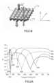
- FIG. 1A represents a diagram illustrating a (partial) sectional view of an example of an optical security component according to the present description.
- the optical security component 101 represented on the FIG. 1A represents for example an optical security component intended to be transferred onto a document or a product with a view to securing it.
- it comprises a support film 111, for example a film of polymer material, for example a film of polyethylene terephthalate (PET) of a few tens of micrometers, typically 15 to 100 ⁇ m, as well as a layer of detachment 112 (optional), for example in natural or synthetic wax.
- PET polyethylene terephthalate
- detachment 112 optionally a layer of detachment 112 (optional), for example in natural or synthetic wax.
- the detachment layer makes it possible to remove the polymer support film 111 after transfer of the optical component to the product or document to be secured.
- the optical security component 101 also comprises a first layer of so-called “low index” dielectric material 113, transparent in the visible, having a first refractive index n 1 and a second layer of so-called “high index” dielectric material 114, transparent in the visible, in contact with the first low index layer 113, and having a second refractive index n 2 .
- the difference between the second refractive index and the first refractive index is greater than or equal to 0.5, hence the designation first “low index” dielectric layer 113 and second “high index” dielectric layer 114.
- the component security optics 101 further comprises a metallic layer 115 in contact with the second layer of high index dielectric material 114.
- the first layer of low index dielectric material 113, the second layer of high index dielectric material 114 and the metallic layer 115 form a first continuous double dielectric-dielectric-metal interface I, comprising a first dielectric-dielectric interface and a first dielectric interface -metal.
- the double interface I is structured to form, in at least a first coupling zone Z 1 , a first coupling network C 1 in two dimensions, an example of which is illustrated in the Fig. 1B which will be described in more detail later.
- continuous double interface it is understood that all of the layers 113, 114, 115 which constitute the double interface I are deposited continuously, that is to say without interruptions, on at least one region comprising said first zone of coupling.
- the double interface I is structured to form a plurality of adjoining zones Z 1 , Z 2 , Z 3 , including the first coupling zone Z 1 , and all the layers 113 , 114, 115 are continuous over the plurality of said areas.
- the optical security component 101 also comprises a protective layer 116, made of dielectric material and in contact with the metallic layer 115.
- the protective layer 116 can also form an adhesive layer or a protective layer.
- the protective layer 116 can also form a third layer of dielectric material, transparent in the visible, having a third refractive index n 3 and forming a second dielectric-metal interface, said second dielectric-metal interface being continuous and structured in the same way as the double interface I.
- the optical security component may also comprise one or more layers (not shown on the FIG. 1A ) not optically functional but suitable for the application, for example, an adhesive layer if the layer 116 does not already form an adhesive layer, for example a heat-reactivable adhesive layer, for the transfer of the optical security component on the product or document.
- the detachment layer 112 can be discontinuous, for example for the formation of a label.
- the adhesive layer can have a permanent adhesive power so that an intermediate support is used to allow manipulation of the component before its application to the document or the product to be protected.
- the optical security component can be manufactured by stacking the layers on the support film 111, then the component is transferred onto a document/product to be secured using the adhesive layer.
- the support film 111 can then be detached, for example by means of the detachment layer 112.
- the main observation face 100 A of the optical security component (or first observation face) is thus on the side of the first layer 113 opposite the etched face of layer 113.
- the optical security component may be intended for securing banknotes; it is for example a track applied by hot gluing, part of a security thread intended to be integrated into the paper during the manufacture of the note.
- the optical security component comprises as previously a support film 111 (12 to 25 ⁇ m) which will also serve as a protective film for the security thread, but not as a detachment layer.
- the optical security component can also comprise in these other examples, in addition to the protective layer 116, optional layers, such as a protective layer, for example a second polymer film or a varnish.
- the manufacture can be carried out by stacking the layers on the support film 111.
- optical security component may be visible from both sides.
- said at least one first coupling network C 1 an example of which is illustrated in a 3-dimensional view on the Fig.
- the first coupling network C 1 is determined to generate a first plasmon resonance effect at said at least one first dielectric-metal interface in a first resonance spectral band.
- the coupling network is formed in this example by two sets of undulations extending along the two directions X, Y to form a two-dimensional structure. In this example, the two directions are perpendicular.
- the network is characterized by the pitch (or period) of each set of ripples in each of the X and Y directions, the depth or amplitude of the ripple (defined as the height between the peak and the trough), the profile of the network according to each direction and the duty cycle according to each direction.
- the depth of the network is advantageously between 10% and 80% of the pitch of the network, advantageously between 10% and 50%.
- the profile of the undulations is for example sinusoidal or quasi-sinusoidal, or more generally with continuous variation as illustrated in the Fig. 1B , this type of profile allowing better propagation of the plasmonic modes and being compatible with fabrication methods by photolithography.
- Other two-dimensional coupling network profiles are possible, whether symmetrical, asymmetrical or asymmetrical networks.
- an electromagnetic surface wave can propagate associated with a collective oscillation of electrons on the surface, called the surface plasmon.
- This phenomenon is for example described in the basic work of H. Raether (“Surface plasmons”, Springer-Verlag, Berlin Heidelberg).
- the coupling of an incident light wave to a plasmonic mode can be obtained in various ways, in particular by structuring the interface to form a coupling network, for example a coupling network as described by means of the Fig. 1B .
- an incident wave of wavelength ⁇ , of polarization TM transverse magnetic wave
- ⁇ incident wave
- TM transverse magnetic wave
- the polarization wave TM is moreover incident on the grating with an azimuth of 0° with respect to the grating defined by the grating vector k gx and an angle of incidence ⁇ in the layer 113 with respect to the axis Z normal to the network map.
- coupling i.e.
- the incident light energy in the dielectric medium is coupled with the plasmon mode, resulting in the absorption of this energy in the metallic layer. This results in a modification of the spectrum of the reflected light energy.
- the optical security component thus behaves like a color band-stop filter for incident radiation in TM mode.
- part of the incident radiation will be coupled with a plasmonic mode thanks to a set of undulations along one direction, and another part of the radiation will be coupled to a plasmonic mode thanks to the set of undulations along another direction, resulting in the absorption in the metallic layer in a first spectral band resulting from the coupling at the various coupling wavelengths previously described.
- the metal layer is of finite thickness and, moreover, that its thickness is of the order of magnitude of the depth of penetration of the electromagnetic field of the plasmon mode in the metal (which is approximately 1/(k 0 (n sp 2 +Re(
- the electromagnetic field of the plasmon mode at the upper interface of the metallic layer “sees” also the lower interface and must therefore also satisfy the boundary conditions of the fields at this lower interface.
- plasmon modes that can propagate along the metallic layer, both of which have a field maximum at the upper and lower interfaces of the metallic layer: a plasmon mode whose magnetic field transverse H is even (therefore the longitudinal electric field, responsible for the longitudinal oscillation of the electrons, odd, with a passage through zero in the metallic layer), known as the "long range” plasmon mode, and a plasmon mode whose H field is odd, more strongly absorbed by the metal, called the "short range” plasmon mode.
- the effective indices are close when the thickness of the metal layer is not too low (greater than 15 nm, for example) and these modes are both coupled in the presence of a grating when the incident wave emanates from a spatially and temporally incoherent light source such as a lighting lamp or natural sunlight.
- the field of the two coupled (or "excited") plasmon modes has a maximum at the lower interface of the metallic layer as well and can therefore, thanks to the presence of the grating, radiate into the transmitted medium (layer 116, Fig. 1A ) and thus allow light energy to pass through the continuous metallic layer and thus produce a peak in transmission, hence the term resonant transmission.
- the effective index of the plasmon (equation (2) above) is determined by the refractive index n 1 of the first layer of low index dielectric material 113 but also by the refractive index n 2 of the second layer of high index dielectric material 114.
- the presence of the layer of high index dielectric material thus causes a displacement of the first spectral band with respect to a single dielectric-metal interface.
- the applicant has also demonstrated for the first time in the field of security an additional effect resulting from the layer of high index dielectric material and which results in original colored effects, in particular tint angles not observed in the optical security components of the state of the art.
- the thickness of the second layer of high-index dielectric material 114 is determined, depending in particular on the nature of the materials and the characteristics of the coupling network, to generate an effect of hybrid plasmon resonance, in a second spectral band of resonance different from said first spectral band.
- the reflection is observed on the side of the first observation face 100 A .
- the coupling grating C 1 is a two-dimensional grating with a period of 280 nm in each direction, a sinusoidal profile with a depth of 42 nm (aspect ratio of 0.15).
- the refractive index of the transparent dielectric material layers 113, 116 is 1.5 and the metal layer is a 25 nm aluminum layer allowing the coupling of plasmon modes at the two metal-dielectric interfaces 114/115 and 115/116; this results in resonant transmission effects.
- the curves are calculated respectively in the following cases: no layer of high index dielectric material (curve 21 R ), layer of high index dielectric material (114, Fig. 1A ) with a refractive index of 2.4 (ZnS) and a thickness of 30 nm (curve 22 R ), layer of high index dielectric material (114, Fig.
- the curves are calculated using the commercial software MC Grating SoftwareC.
- the curve 21 R shows a first unique resonance spectral band corresponding to a dip in the normalized reflection curve referenced 210. This is a classic normalized reflection curve resulting from a plasmon effect at a dielectric-metal interface simple.
- curve 22 R When a layer of high-index dielectric material is introduced (curve 22 R ), a shift in the first spectral resonance band is observed resulting from the variation in the effective index of the plasmonic mode (hollow 220).
- the second resonance spectral band results from a “hybrid” plasmonic mode in which the energy of the electromagnetic field remains maximum at the surface of the metal but diffuses into the layer of high-index dielectric material.
- the third spectral resonance band results from resonances of guided modes in the layer of high index dielectric material.
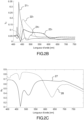
- THE Figs. 3A - 3C represent images of the electric field modulus determined in the near field, and more precisely the Ey component of the field, that is to say the projection of the electric field on the Y axis. the images are calculated with the software MC Grating Software ⁇ .
- the near-field calculation makes it possible to reveal the particular characteristics of the different resonances present in the system. This helps to know where the energy of the field is concentrated. In particular, we observe that the energy of the hybrid mode ( Fig. 3B ) is less concentrated at the metal surface than that of the purely plasmonic mode ( Fig. 3A ). This amounts to saying that the hybrid mode has a lower effective index than the pure plasmonic mode. As explained previously, the hybrid mode depends on the second layer of high index dielectric material and can only exist and be coupled effectively if the thickness of the second layer of high index dielectric material is sufficiently great.
- the second layer of high index dielectric material is very thick ( Fig. 3C )
- a guided mode in the thickness of the second layer of high-index dielectric material (and not on the surface of the metal).
- the effective index of the guided mode is even lower than the effective indices of the hybrid and plasmonic modes. It does not have analytical formulas making it possible to determine the effective indices of the modes, but the simulations of electromagnetic fields carried out by the applicant have made it possible to highlight the various modes which appear with an increasing thickness of the second layer in high dielectric material. hint.
- the appearance of the second resonance spectral band makes it possible to show colored effects in reflection and at zero order with original colors, presenting hue angles that cannot be obtained with the plasmonic structures of the state of the art.
- the commercial software MC Grating Software ⁇ is used, which makes it possible to calculate the diffraction efficiencies for different types of structures.
- There are other software which can also be used such as for example the software S 4 or S4 (Stanford Stratified Structure Solver) or the software developed by the company LumericalC.
- the profile of the network is defined according to each of the directions, for example by means of Fourier harmonics.
- Two semi-infinite media are then defined corresponding to the layers of low index dielectric material 113, 116 ( Fig. 1A ), whose refractive index is for example 1.5.
- the depth of the grating and the thickness of the metal layer are chosen so as to adjust the resonance amplitudes to have the most effective coupling possible, i.e. a maximum hollow amplitude and a minimum of the hollows corresponding to the spectral resonance bands tending towards 0.
- the transmission is observed from the side of the second observation face 100 B when the component is illuminated from the side of the face 100 A or from the side of the observation face 100 A when the component is illuminated from the side of the face 100 B .
- the conditions are identical to the conditions used to determine the curves represented on the Fig. 2A .
- the curves 21 T , 22 T , 23 T , 24 T correspond respectively to the curves calculated without a layer of high index dielectric material, with a layer of high index dielectric material with a refractive index of 2.4 (ZnS) and a thickness 30 nm, with a layer of high index dielectric material with a refractive index of 2.4 and a thickness of 60 nm, with a layer of high index dielectric material with a refractive index of 2.4 and a thickness of 90 nm.
- FIG. 2C illustrates the influence of polarization on normalized reflection.
- the thickness of the layer of dielectric material is 80 nm.
- a normalized reflection curve in TM polarization (curve 27) different from the normalized reflection curve in TE polarization (curve 28) is observed.
- This polarization dependence allows authentication of the additional optical security component compared to authentication with the naked eye, in natural light.
- the optical security component in natural light and observation, through a polarizer, of a change in color of the colored effect as a function of the direction of polarization; or an illumination of the optical security component in linear polarized light and the observation of a color change of the colored effect as a function of the direction of the polarization.
- the coupling network is chosen with a square mesh (identical periods according to the two directions), also the effect of the polarization will be visible with a non-zero incidence.
- the authentication can also be done at normal incidence.
- an optical security component with at least a first double interface structured to present at least a first coupling zone comprising a first coupling network with a square mesh and at least a second coupling zone comprising a second coupling network with a non-square rectangular mesh.
- a control in polarization at normal incidence will allow the observation of a change of color with change of the polarization only in the second coupling zone.
- authentication by polarization analysis can be done with the naked eye as described above or by equipment such as an automatic control machine (document reader type, for example, such as those used to control passports or banknotes) or any other control equipment incorporating a white light source, a polarizing filter, a sensor, a data processing unit.
- equipment such as an automatic control machine (document reader type, for example, such as those used to control passports or banknotes) or any other control equipment incorporating a white light source, a polarizing filter, a sensor, a data processing unit.
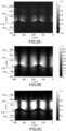
- THE Figs. 4A - 4C illustrate the authentication of an optical security component 42 according to an embodiment, said component 42 being arranged on a substrate 41 of a secure document 40. Authentication is done with the naked eye, in non-polarized white light .
- the optical security component is in this example a component as described on the Fig. 1A , in which the double interface I has 3 contiguous zones Z 1 , Z 2 , Z 3 .
- the first zone Z 1 is structured with a first coupling network C 1
- the second zone Z 2 is structured with a second coupling network C 2 different from the first coupling network and the zone Z 3 is not structured.
- the three areas are contiguous and arranged to form a recognizable pattern, for example an "R" as shown in the Fig. 4A .
- the layer of metal 115 is assumed to be thin enough to allow a resonant transmission effect, as illustrated in the Fig. 2B .
- THE Figs. 4B, 4C and 4D show the observation respectively in reflection according to the first observation face 100 A , in reflection according to the second observation face 100 B , opposite to the first observation face, and in transmission.
- the position of the lighting source is referenced SRC and the position of the observer relative to the lighting source is symbolized by an eye OBS.
- the Fig. 10 shows a diagram illustrating the CIE Lab sphere adopted by the Comotti International de l'Eclairage (CIE) in 1976 and defined according to ISO 11664-4.
- the hue angle h ab indicates the color; it evolves from red (angle 0°) to yellow (90°) then to green (180°) then to blue (270°).
- the applicant has shown the possibility of obtaining colors by means of the optical security component with all tint angles and in particular tint angles between 120° and 320°, that is to say between green and violet, passing through shades of blue close to cyan, colors which were not obtained with the plasmonic components of the state of the art.
- zone Z 3 will appear reflective because it is unstructured. It is remarkable to note that the 3 zones Z 1 , Z 2 and Z 3 and the corresponding visual effects can be identified very precisely (junctions between the zones referenced 118 on the Fig. 1A ) because these colored effects result from the structures of the different zones and not from the local deposition of an additional layer of a material (for example pigment or dye). Indeed, the local deposition of an additional layer, for example by printing, requires providing a minimum distance between two regions of different colors.
- a material for example pigment or dye
- multicolored images for example images formed of pixels, each pixel corresponding to an area and having for example dimensions less than 300 ⁇ m and not visible to the naked eye or, on the contrary, areas more large identifiable with the naked eye, as in the example of the Figs. 4A - 4C .
- Fig. 4C schematizes the same document secured by means of the same optical security component 42 but seen in reflection from the side of the second observation face 100 B . Seen from this side, the colored effect results from a plasmonic effect at the simple metal dielectric interface (115/116, Fig. 1A ). The colors observed in the coupling zones Z 1 , Z 2 are therefore different from those observed along the main observation face 100 A . Again, zone Z 3 appears reflective because it is unstructured.
- Fig. 4D schematizes the same secure document by means of the same optical security component 42 but seen in transmission.
- the colored effects in the zones Z 1 , Z 2 result from a resonant transmission effect as illustrated by means of the curves of the Fig. 2B .
- Zone Z 3 appears black, non-transparent, because it is unstructured.
- the effect in reflection is substantially the same as the effect in reflection in the case where a thick metallic layer would have been used.
- the hue does not change but the luminance is modified, that is to say the light or dark side of the color.
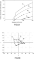
- Fig. 5A represents a diagram illustrating curves showing the spectral position of the hybrid mode as a function of the thickness of the second layer of dielectric material (high index), in the case of a coupling network having a square mesh and for different values of the period, in an example of an optical security component according to the present description. The observation is made in reflection, at normal incidence.
- the material chosen is ZnS (refractive index 2.4)
- the metal layer is a 25 nm thick aluminum layer
- the layers in low index material have a refractive index of 1.5
- the coupling grating has a sinusoidal profile in each direction, a constant aspect ratio equal to 0.15, a square mesh with a period in each direction of 200 nm (curve 51) , 240 nm (curve 52), 280 nm (curve 53), 320 nm (curve 54).
- the choice of the period, for different values of the thickness of the layer of high index dielectric material makes it possible to influence the spectral position of the hybrid mode (trough of the normalized reflection). It is observed in this example that a minimum thickness of 45 nm of ZnS is required to observe the hybrid mode.
- Fig. 5B represents a diagram illustrating the colors that can be obtained (representation ab, see Fig. 10 ), by varying the period of the coupling grating between 220 nm and 350 nm, in the same example of optical security component as that used for the Fig. 5A , for a ZnS thickness of 60 nm (curve 57). This curve is compared with a curve obtained without ZnS (curve 55) and with a ZnS thickness of 20 nm (curve 56).
- the tint angles that can be obtained with an optical security component according to the present description (curve 57) in which the hybrid plasmonic mode is present are different from those obtained with an optical security component according to the state of the art (curve 55) or with an optical security component in which the high index layer thickness is too low to obtain the hybrid mode (curve 56).
- the optical security component has a single first double dielectric-dielectric-metal interface.
- the optical security component has a second double dielectric-dielectric-metal interface, as illustrated in a partial 3D view on the Fig. 6A .
- the optical security component further comprises layers of dielectric material 113, 114, 116 already described, a fourth layer of dielectric material 117, in contact with the metallic layer 115 on the side opposite the side in contact with the second layer of dielectric material 114.
- the third layer of dielectric material 116 (not shown in the Fig. 6A ) is in contact with said layer of dielectric material 117.
- the third layer of dielectric material 116 has a third refractive index n 3 and the fourth layer of dielectric material 117 has a fourth refractive index n 4 such that the index difference between n 4 and n 3 is greater than 0.5.
- the third layer of dielectric material 116 then forms a second “low index” layer and the fourth layer of dielectric material 117 forms a second “high index” layer.
- the thickness of the fourth layer of “high index” dielectric material 117 it is possible by choosing in particular the thickness of the fourth layer of “high index” dielectric material 117 to also obtain according to a second observation face (100 B , Fig. 1A ) opposite the first observation face (100 A , Fig. 1A ) a hybrid plasmon resonance effect as described above and therefore remarkable colored effects.
- Fig. 6B thus represents a diagram illustrating a first colored effect visible in reflection, according to the first observation face, with an optical security component 62 arranged on a substrate 61 of a secure document 60, the optical security component having a first and a second double-interfaces, in which the double interfaces are structured according to the same pattern as that illustrated in the Fig. 4A .
- the metal layer is assumed to be thin enough to observe plasmon resonance effects in transmission.
- Fig. 6C schematizes the same document secured by means of the same optical security component 62 but seen in reflection from the side of the second observation face 100 B (back). Seen from this side, in this example, the colored effect is identical to that observed from the side of the main observation face (recto) since, for example, identical thicknesses and indices of the high-index dielectric layers 114, 117 will have been chosen. However, it is also possible to choose different high-index dielectric layers 114, 117, in which case the colors observed in the coupling zones Z 1 , Z 2 will be different from those observed along the main observation face 100a. on the other hand, the unstructured zone Z 3 always appears reflective, uncoloured.
- Fig. 6D schematizes the same secure document by means of the same optical security component 62 but seen in transmission.
- the colored effects in the zones Z 1 , Z 2 result from a resonant transmission effect as illustrated by means of the curves of the Fig. 2B but influenced by the second high index layer 117.
- Zone Z 3 appears black, non-transparent, because it is unstructured.
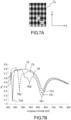
- Fig. 7A thus represents a diagram illustrating a top view of a coupling network C 3 with different periods p x , p y along the first and second directions X, Y, in an example of an optical security component according to the present description.
- the directions are perpendicular to each other, but it is also possible to have two directions which have between them an angle different from the right angle, for example an angle between 30° and 60°.
- the X axis is in this example included in the incidence plane and the Y axis is perpendicular to the incidence plane.
- the curves are calculated with a two-dimensional network of the type from that shown on the Fig.
- the double interface comprises a metallic layer in aluminum, 25 nm thick, and a layer of high index dielectric material in ZnS (refractive index 2.4) 80 nm thick.
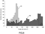
- FIG. 8 represents a diagram illustrating a histogram of the tint angles in an optical security component according to the present description (histogram 82), and in an optical security component according to the state of the art (histogram 81).
- the histogram 82 shows the occurrence of structures for each hue angle between 0° and 350° in a structure of the type shown in the Fig. 1A (two-dimensional square-mesh coupling network). More precisely, the histogram 82 is obtained by varying the period between 230 nm and 300 nm, the grating depth between 40 nm and 120 nm, the thickness of the metal (aluminum) layer between 10 nm and 35 nm and the layer of high index dielectric material between 50 and 140 nm.
- the grating profile is sinusoidal along each of the directions, the refractive index of the layer of low index dielectric material is 1.5 and the refractive index of the layer of high index dielectric material is 2.4.
- histogram 81 shows the occurrence of structures for each hue angle in a structure similar to that used to obtain histogram 81 but in which the thickness of the high index dielectric layer is between 0 and 40 nm.
- the other parameters vary in the same way as for histogram 82.
- a method of manufacturing optical security components according to the present description advantageously comprises the following steps.
- the optical structure formed from said at least one first coupling grating or from a microscopic structure modulated by said at least one first coupling grating is recorded by photolithography or electron beam lithography on a photosensitive support (or "photoresist” according to the Anglo-Saxon expression).
- An electroplating step makes it possible to transfer the optical structure into a resistant material, for example based on nickel, to produce a metal matrix or “master” comprising the optical structure.
- the manufacture of the optical security component then comprises a replication step.
- the replication can be carried out by stamping (by hot pressing of the dielectric material in English “hot embossing”) of the first layer 113 ( Fig.
- n 1 low index layer
- layer 113 is advantageously carried by support film 111, for example a 12 ⁇ m to 100 ⁇ m film of polymer material, for example PET (polyethylene terephthalate).
- the replication can also be made by molding the layer of stamping varnish before drying then UV curing (“UV casting”). Replication by UV crosslinking makes it possible in particular to reproduce structures having a large depth amplitude and makes it possible to obtain better fidelity in the replication.
- any other high-resolution replication method known from the prior art can be used in the replication step. Then comes the deposition on the layer thus embossed of all the other layers, in particular the second layer of dielectric material 114 (high index layer), the metallic layer 115, and the other possible layers, including for example the protective layer 116 .
- an optical security component according to the present description in a secure document is perfectly compatible with the presence in the same document of structures based on networks usually used for the production of holographic components.
- an optical security element comprising one or more components of the plasmonic type as described previously and one or more other types of optical security components known to the state of the art, for example of the holographic type. .
- a matrix can be produced by recording the different patterns corresponding to the different optical security components on the photoresist support, this step being followed by an electroplating step. Stamping can then be carried out from the die to transfer the various microstructures onto the film of polymer material, intended for embossing.
- the metallic layer and/or the layer of high-index dielectric material, the thicknesses of which are controlled for the optical security components with plasmonic effect according to the present description, may be deposited over the entire film, or selectively at the level of the optical component. safety according to this description.
- selective deposition of reflective layers makes it possible, for example, to further highlight the optical effects of said components according to the present description and/or to reveal the substrate of the document or of the object to be secured in the form of patterns. not reflective.
- Selective metallization can be obtained by a first step of depositing a metallic layer (respectively high index layer) on the whole of the structured film then by partial demetallization (respectively partial removal of the high index layer) to form said non-metallized areas (respectively without high index layer).
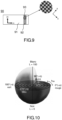
- Fig. 9 represents a secure document 90, for example a value document of the banknote type, thus equipped with a security element 92 comprising an optical security component 93 according to the present description.
- the security element 92 is in the form of a strip, typically 15 mm wide, which is attached to a substrate 91 of the document 90.
- the security element 92 is attached to the substrate by known means.
- the security element can be fixed by heat transfer reactivating a transparent adhesive layer previously applied to the protective layer 116.
- a detachment layer 112 (for example a wax) can be applied between the varnish stamping 113 and the PET support film 111 ( Fig. 1A ).
- the security element is transferred to the document by hot pressing the element security on the document, the plasmonic component facing the transparent area. During the transfer, the adhesive film sticks on the substrate 91 of the document and the release layer as well as the support film can be removed.
- a window of transparency can be provided at the level of the component of plasmonic type according to the present description if the latter is provided to be visible in transmission. Note that if the transparency window corresponds to a transparent substrate, then the support film can be effectively removed, as described above. If the transparency window corresponds to a hole in the paper, then the security element is glued and the support film retained.
- the secure document thus obtained is very easily controllable with the naked eye, in white light, by an inexperienced user, and with great reliability.
- Visual authentication of the secure document is therefore possible, including in natural light.
- This authentication based on visual effects in reflection and possibly in transmission, is particularly easy to achieve.
- authentication is also possible by illuminating the optical security component in linearly polarized light, or by illuminating the optical security component in natural light and observing it through a linear polarizer .
- the change in polarization will cause a change in color to appear, as explained above with reference to the Fig. 2C .
- Machine control is also possible, for example control by smartphone. Indeed, due to the very different tint angles that can be obtained by means of the optical security component, it will be possible for example to determine whether the angular difference between two tint angles corresponding to two coupling zones is respected. .
- the optical security component according to the present description comprises various variants, modifications and improvements which will appear obvious to those skilled in the art, it being understood that these various variants , modifications and improvements fall within the scope of the invention as defined by the following claims.
Landscapes
- Physics & Mathematics (AREA)
- General Physics & Mathematics (AREA)
- Health & Medical Sciences (AREA)
- General Health & Medical Sciences (AREA)
- Toxicology (AREA)
- Optics & Photonics (AREA)
- Spectroscopy & Molecular Physics (AREA)
- Credit Cards Or The Like (AREA)
- Diffracting Gratings Or Hologram Optical Elements (AREA)
- Optical Modulation, Optical Deflection, Nonlinear Optics, Optical Demodulation, Optical Logic Elements (AREA)
Description
La présente description concerne un composant optique de sécurité à résonance plasmonique et un procédé de fabrication d'un tel composant. Le composant optique de sécurité selon la présente description s'applique notamment au marquage de sécurité pour l'authentification d'objets de valeurs, et plus précisément l'authentification à l'oeil nu par observation en réflexion et/ou en transmission.The present description concerns an optical security component with plasmon resonance and a method for manufacturing such a component. The optical security component according to the present description applies in particular to security marking for the authentication of objects of value, and more precisely authentication with the naked eye by observation in reflection and/or in transmission.
On connaît de nombreuses technologies pour l'authentification d'objets de valeur et notamment l'authentification de documents de valeur, tels que les billets de banque ou documents de voyage (passeports, cartes d'identité ou autres documents d'identification), ou pour l'authentification de produits au moyen d'étiquettes de marquage. Ces technologies visent à la production de composants optiques de sécurité dont les effets optiques en fonction des paramètres d'observation (orientation par rapport à l'axe d'observation, position et dimensions de la source lumineuse, etc.) prennent des configurations caractéristiques et vérifiables. Le but général de ces composants optiques est de fournir des effets nouveaux et différenciés, à partir de configurations physiques difficilement reproductibles ou imitables par un faussaire.Many technologies are known for the authentication of valuables and in particular the authentication of valuable documents, such as banknotes or travel documents (passports, identity cards or other identification documents), or for the authentication of products by means of marking labels. These technologies are aimed at the production of optical security components whose optical effects depending on the observation parameters (orientation with respect to the axis of observation, position and dimensions of the light source, etc.) take on characteristic configurations and verifiable. The general purpose of these optical components is to provide new and differentiated effects, from physical configurations that are difficult to reproduce or imitate by a counterfeiter.
Parmi ces composants, les composants optiques de sécurité dits « à résonance plasmonique » permettent de générer des effets colorés en réflexion ou en transmission, qui résultent de l'excitation de plasmons volumiques ou surfaciques lors de l'interaction d'ondes lumineuses incidentes avec des motifs métalliques nanométriques. Les couleurs ainsi produites, dites « structurelles », présentent l'avantage d'être variables en fonction de paramètres d'observation ce qui facilite l'authentification. Par ailleurs, contrairement aux composants optiques de sécurité basés sur des effets purement diffractifs, comme les composants holographiques par exemple, les composants optiques de sécurité à résonance plasmonique ont l'avantage de présenter des effets visuels à l'ordre zéro (réflexion spéculaire ou transmission directe), plus difficiles à reproduire du fait des très petites dimensions des structures mais faciles à authentifier.Among these components, so-called "plasmon resonance" safety optical components make it possible to generate colored effects in reflection or transmission, which result from the excitation of volume or surface plasmons during the interaction of incident light waves with nanoscale metal patterns. The colors thus produced, called “structural”, have the advantage of being variable according to observation parameters, which facilitates authentication. Furthermore, unlike optical security components based on purely diffractive effects, such as holographic components for example, plasmon resonance optical security components have the advantage of presenting visual effects at zero order (specular reflection or transmission direct), more difficult to reproduce due to the very small dimensions of the structures but easy to authenticate.
La demande de brevet publiée
La demande de brevet
La demande de brevet
Dans cette même demande de brevet
La demande
La présente description présente un composant optique de sécurité à résonance plasmonique, présentant, notamment en réflexion, des effets colorés originaux et distinctifs par rapport à ceux décrits dans les composants optiques de sécurité de l'état de l'art, permettant une authentification encore plus facile et fiable, y compris à l'oeil nu par un utilisateur non initié.The present description presents a plasmon resonance optical security component, presenting, in particular in reflection, original and distinctive colored effects compared to those described in the optical security components of the state of the art, allowing an even more easy and reliable, including with the naked eye by an uninitiated user.
Selon un premier aspect, la présente description concerne un composant optique de sécurité à effet plasmonique, ledit composant pouvant être contrôlé à l'oeil nu, en réflexion, selon au moins une première face d'observation.According to a first aspect, the present description relates to an optical security component with a plasmonic effect, said component being able to be checked with the naked eye, in reflection, according to at least one first observation face.
Le composant optique de sécurité selon le premier aspect comprend :
- au moins une première couche en matériau diélectrique, transparente, présentant un premier indice de réfraction,
- au moins une deuxième couche en matériau diélectrique, transparente, d'épaisseur comprise entre 20 nm et 150 nm, présentant un deuxième indice de réfraction, la différence entre le deuxième indice de réfraction et le premier indice de réfraction étant supérieure ou égale à 0,5 et ladite deuxième couche en matériau diélectrique étant en contact avec ladite première couche en matériau diélectrique, et
- une couche métallique en contact avec ladite au moins une deuxième couche en matériau diélectrique.
- at least a first layer of dielectric material, transparent, having a first refractive index,
- at least one second layer of dielectric material, transparent, with a thickness of between 20 nm and 150 nm, having a second refractive index, the difference between the second refractive index and the first refractive index being greater than or equal to 0, 5 and said second layer of dielectric material being in contact with said first layer of dielectric material, and
- a metal layer in contact with said at least one second layer of dielectric material.
Selon l'invention, ladite première couche en matériau diélectrique, ladite deuxième couche en matériau diélectrique et ladite couche métallique forment une première double interface diélectrique-diélectrique-métal, comprenant une première interface diélectrique-diélectrique et une première interface diélectrique-métal, et structurée pour former, dans au moins une première zone de couplage, un premier réseau de couplage à deux dimensions avec une première direction et une deuxième direction, présentant une première période comprise entre 150 nm et 350 nm selon la première direction et une deuxième période comprise entre 150 nm et 350 nm selon la deuxième direction.According to the invention, said first layer of dielectric material, said second layer of dielectric material and said metallic layer form a first double dielectric-dielectric-metal interface, comprising a first dielectric-dielectric interface and a first dielectric-metal interface, and structured to form, in at least a first coupling zone, a first two-dimensional coupling network with a first direction and a second direction, having a first period comprised between 150 nm and 350 nm along the first direction and a second period between 150 nm and 350 nm along the second direction.
Selon l'invention, ledit premier réseau de couplage est déterminé pour générer un premier effet de résonance plasmonique à ladite au moins une première interface diélectrique-métal dans une première bande spectrale de résonance et l'épaisseur de ladite au moins une deuxième couche en matériau diélectrique est déterminée pour générer, au moyen dudit premier réseau de couplage, un effet de résonance plasmonique hybride, dans une deuxième bande spectrale de résonance différente de ladite première bande spectrale. Dans la présente description, ladite première couche en matériau diélectrique est également appelée couche en matériau diélectrique « bas indice » et ladite deuxième couche en matériau diélectrique est également appelée couche en matériau diélectrique « haut indice ». Plus généralement, une couche en matériau diélectrique dite « haut indice » n'est définie qu'en relation avec une couche en matériau diélectrique dite « bas indice » avec laquelle elle est en contact, une différence entre l'indice de réfraction de la couche en matériau diélectrique haut indice et l'indice de réfraction de la couche en matériau diélectrique bas indice étant supérieure ou égale à 0,5.According to the invention, said first coupling network is determined to generate a first plasmon resonance effect at said at least one first dielectric-metal interface in a first resonance spectral band and the thickness of said at least one second layer of material dielectric is determined to generate, by means of said first coupling network, a hybrid plasmon resonance effect, in a second resonance spectral band different from said first spectral band. In the present description, said first layer of dielectric material is also called layer of “low index” dielectric material and said second layer of dielectric material is also called layer of “high index” dielectric material. More generally, a layer of so-called "high index" dielectric material is only defined in relation to a layer of so-called "low index" dielectric material with which it is in contact, a difference between the refractive index of the layer made of high index dielectric material and the refractive index of the layer of low index dielectric material being greater than or equal to 0.5.
La déposante a montré que le choix d'une épaisseur suffisante de la couche en matériau diélectrique haut indice entraîne non seulement un décalage de la première bande spectrale de résonance plasmonique à l'interface diélectrique-métal mais également la génération d'un deuxième effet de résonance plasmonique, dit « hybride » dans une deuxième bande spectrale différente de la première bande spectrale. La déposante a montré que lors de la génération du premier effet de résonance plasmonique, décrit dans l'état de l'art, le champ électromagnétique est confiné à la surface du métal. Lors de la génération du deuxième effet de résonance plasmonique, l'énergie du champ électromagnétique reste maximale à la surface du métal mais diffuse dans la couche en matériau diélectrique haut indice, d'où le terme d'effet « hybride ».The applicant has shown that the choice of a sufficient thickness of the layer of high index dielectric material leads not only to a shift in the first spectral band of plasmon resonance at the dielectric-metal interface but also to the generation of a second effect of plasmon resonance, called "hybrid" in a second spectral band different from the first spectral band. The applicant has shown that during the generation of the first plasmon resonance effect, described in the state of the art, the electromagnetic field is confined to the surface of the metal. During the generation of the second plasmon resonance effect, the energy of the electromagnetic field remains maximum at the surface of the metal but diffuses into the layer of high-index dielectric material, hence the term “hybrid” effect.
Une bande spectrale de résonance au sens de la présente description peut être définie comme une plage continue de longueurs d'onde pour lesquelles on observe un creux dans la courbe de réflexion normalisée du composant optique de sécurité, lorsque le composant est éclairé en lumière blanche à incidence normale, le creux étant caractérisé par un maximum local et un minimum local consécutifs, pour lesquels une différence entre les valeurs de la réflexion normalisée est strictement supérieure à 0,2 (ou 20%). Pour chaque bande spectrale de résonance, on peut définir une longueur d'onde centrale de résonance correspondant à la longueur d'onde de ladite bande spectrale pour laquelle la réflexion normalisée présente une valeur minimale. Par bandes spectrales de résonance différentes, on comprend dans la présente description deux bandes spectrales présentant respectivement des longueurs d'onde centrales de résonance distinctes d'au moins 50 nm. La présence des deux bandes spectrales différentes se traduit, notamment lors d'une observation du composant optique de sécurité en réflexion, par des effets colorés originaux par rapport à ceux observés dans l'état de l'art, notamment des couleurs présentant des angles de teinte compris entre 120° et 320° sans ajout de colorants ni de pigments.A spectral resonance band within the meaning of the present description can be defined as a continuous range of wavelengths for which a dip is observed in the normalized reflection curve of the optical security component, when the component is illuminated in white light at normal incidence, the dip being characterized by a local maximum and a consecutive local minimum, for which a difference between the values of the normalized reflection is strictly greater than 0.2 (or 20%). For each resonance spectral band, it is possible to define a central resonance wavelength corresponding to the wavelength of said spectral band for which the normalized reflection has a minimum value. The term “different resonance spectral bands” means in the present description two spectral bands having respectively distinct central resonance wavelengths of at least 50 nm. The presence of the two different spectral bands is reflected, in particular when observing the optical security component in reflection, by original colored effects compared to those observed in the state of the art, in particular colors having angles of shade between 120° and 320° without adding dyes or pigments.
Dans la présente description, une couche en matériau diélectrique transparent est définie comme une couche présentant une transmission d'au moins 70%, de préférence au moins 80% pour une longueur d'onde comprise dans la bande spectrale visible, soit entre 400 nm et 800 nm.In the present description, a layer of transparent dielectric material is defined as a layer having a transmission of at least 70%, preferably at least 80% for a wavelength included in the visible spectral band, i.e. between 400 nm and 800nm.
Dans la présente description, un réseau à deux dimensions ou réseau « croisé » est un réseau défini par la superposition de deux ensembles d'ondulations périodiques s'étendant selon deux directions. On peut définir pour chaque ensemble d'ondulations un vecteur réseau comprenant une direction perpendiculaire aux ondulations et une norme inversement proportionnelle à la période.In the present description, a two-dimensional grating or "crossed" grating is a grating defined by the superposition of two sets of periodic undulations extending in two directions. It is possible to define for each set of undulations a grating vector comprising a direction perpendicular to the undulations and a norm inversely proportional to the period.
Selon un ou plusieurs exemples de réalisation, le profil dudit au moins un premier réseau à deux dimensions est à variation continue selon chaque direction, ce type de profil permettant notamment une meilleure propagation des modes plasmoniques. Par exemple, le profil dudit au moins un premier réseau selon chaque direction est sinusoïdal ou quasi-sinusoïdal, c'est-à-dire avec un rapport cyclique différent de 0,5. Le rapport cyclique est défini sur une période présentant un creux et un pic d'ondulation, comme le rapport de la longueur présentant une valeur supérieure à la valeur moyenne entre le pic et le creux et la période.According to one or more exemplary embodiments, the profile of said at least one first two-dimensional grating is continuously variable in each direction, this type of profile allowing in particular better propagation of the plasmonic modes. For example, the profile of said at least one first network in each direction is sinusoidal or quasi-sinusoidal, that is to say with a duty cycle different from 0.5. The duty cycle is defined over a period having a trough and a ripple peak, such as the ratio of the length having a value greater than the average value between the peak and trough and the period.
Généralement, ledit au moins un premier réseau à deux dimensions selon la présente description peut être symétrique, asymétrique ou dissymétrique. Par symétrique, on comprend dans la présente description que ledit au moins un premier réseau de couplage est identique vu de la face d'observation ou de la face opposée à la face d'observation. Par dissymétrique, on comprend que ledit au moins un premier réseau de couplage est différent vu de la face d'observation ou de la face opposée à la face d'observation. Un tel réseau dissymétrique est décrit par exemple dans le brevet
Selon un ou plusieurs exemples de réalisation, la première direction et la deuxième direction du réseau de couplage sont sensiblement perpendiculaires. Le réseau à deux dimensions forme ainsi une structure dont la forme est de type « boite d'oeufs ». Par sensiblement perpendiculaires, on comprend que la première et la deuxième direction présentent un angle de 90°± 5°. Un tel composant optique de sécurité présente, dans le cas d'une maille carrée, une stabilité de l'effet coloré lors d'une rotation azimutale entre 0° et 90°. Dans le cas d'une maille rectangulaire non carrée, on pourra observer une variation de l'effet coloré lors d'une rotation azimutale entre 0° et 90°.According to one or more exemplary embodiments, the first direction and the second direction of the coupling network are substantially perpendicular. The two-dimensional network thus forms a structure whose shape is of the “egg box” type. By substantially perpendicular, it is understood that the first and the second direction have an angle of 90°±5°. Such an optical security component has, in the case of a square mesh, a stability of the colored effect during an azimuthal rotation between 0° and 90°. In the case of a non-square rectangular mesh, a variation of the colored effect can be observed during an azimuthal rotation between 0° and 90°.
Selon d'autres exemples de réalisation, la première direction et la deuxième direction du réseau de couplage peuvent présenter un angle différent de 90°, par exemple compris entre 30° et 60°.According to other exemplary embodiments, the first direction and the second direction of the coupling network may have an angle different from 90°, for example between 30° and 60°.
Selon un ou plusieurs exemples de réalisation, la différence entre l'indice de réfraction de la deuxième couche en matériau diélectrique haut indice et l'indice de réfraction de la première couche en matériau diélectrique bas indice est supérieure ou égale à 0,8. Il est alors possible d'exciter des modes hybrides pour des épaisseurs de la couche en matériau diélectrique haut indice plus faibles que si la différence d'indice vaut 0.5.According to one or more exemplary embodiments, the difference between the refractive index of the second layer of high index dielectric material and the refractive index of the first layer of low index dielectric material is greater than or equal to 0.8. It is then possible to excite hybrid modes for thicknesses of the layer of high index dielectric material lower than if the index difference is equal to 0.5.
Selon un ou plusieurs exemples de réalisation, l'épaisseur de ladite au moins une deuxième couche en matériau diélectrique haut indice est comprise entre 20 nm et 100 nm. Au-delà de 100 nm, la couche de matériau diélectrique haut indice peut en effet générer dans des zones non structurées des teintes non voulues. En pratique, l'épaisseur de ladite au moins une deuxième couche en matériau diélectrique haut indice peut être comprise entre 40 nm et 100 nm.According to one or more exemplary embodiments, the thickness of said at least one second layer of high-index dielectric material is between 20 nm and 100 nm. Beyond 100 nm, the layer of high index dielectric material can in fact generate unwanted tints in unstructured areas. In practice, the thickness of said at least one second layer of high index dielectric material can be between 40 nm and 100 nm.
Selon un ou plusieurs exemples de réalisation, ladite au moins une deuxième couche en matériau diélectrique haut indice résulte du dépôt, par exemple un dépôt sous vide, d'une couche de sulfure de zinc (ZnS), dioxyde de titane (TiO2), nitrure de silicium (Si3N4). D'autres exemples de matériaux pour la formation de la couche en matériau diélectrique haut indice sont connus et divulgués, par exemple dans le brevet
Selon un ou plusieurs exemples de réalisation, ladite au moins une première couche en matériau diélectrique bas indice résulte par exemple du dépôt, par exemple un dépôt sous vide, d'une couche organique d'indice optique généralement compris entre 1,4 et 1, 6, par exemple une colle ou une résine. Des exemples de matériaux pour la formation de la couche en matériau diélectrique bas indice sont connus et divulgués, par exemple dans le brevet
Selon un ou plusieurs exemples de réalisation, l'épaisseur de ladite au moins une deuxième couche en matériau diélectrique haut indice est suffisante pour permettre un effet de résonance de modes guidés dans la couche en matériau diélectrique haut indice, dans une troisième bande de résonance distincte de la première et de la deuxième bande de résonance. Dans des exemples de réalisation, la présence de la troisième bande de résonance peut être recherchée pour générer des effets colorés avec d'autres angles de teinte. Dans d'autres exemples de réalisation au contraire, on limitera l'épaisseur de ladite au moins une deuxième couche en matériau diélectrique haut indice pour éviter l'effet de résonance de modes guidés et obtenir l'effet coloré résultant seulement du premier effet de résonance plasmonique et de l'effet de résonance plasmonique hybride.According to one or more exemplary embodiments, the thickness of said at least one second layer of high index dielectric material is sufficient to allow a resonance effect of guided modes in the layer of high index dielectric material, in a third distinct resonance band of the first and second resonance bands. In exemplary embodiments, the presence of the third resonance band can be sought to generate colored effects with other tint angles. In other exemplary embodiments, on the contrary, the thickness of said at least one second layer of high index dielectric material will be limited to avoid the resonance effect of guided modes and to obtain the colored effect resulting only from the first resonance effect. plasmonics and the hybrid plasmon resonance effect.
Selon un ou plusieurs exemples de réalisation, le composant optique de sécurité comprend en outre une troisième couche en matériau diélectrique, transparente, présentant un troisième indice de réfraction, en contact avec ladite couche métallique sur une face opposée à la face de la couche métallique en contact avec la deuxième couche en matériau diélectrique haut indice, pour former une deuxième interface diélectrique-métal, ladite deuxième interface diélectrique-métal étant structurée dans ladite au moins une première zone de couplage selon ledit premier réseau de couplage.According to one or more exemplary embodiments, the optical security component further comprises a third layer of dielectric material, transparent, having a third refractive index, in contact with said metallic layer on a face opposite the face of the metallic layer in contact with the second layer of high-index dielectric material, to form a second dielectric-metal interface, said second dielectric-metal interface being structured in said at least one first coupling zone according to said first coupling network.
Il est alors possible d'observer en réflexion, et selon une deuxième face d'observation opposée à la première face d'observation, un effet coloré résultant d'un effet de résonance plasmonique à la deuxième interface diélectrique-métal.It is then possible to observe in reflection, and according to a second observation face opposite the first observation face, a colored effect resulting from a plasmon resonance effect at the second dielectric-metal interface.
Selon un ou plusieurs exemples de réalisation, le composant optique de sécurité comprend en outre une troisième couche en matériau diélectrique, transparente, présentant un troisième indice de réfraction et une quatrième couche en matériau diélectrique, transparente, d'épaisseur comprise entre 20 nm et 150 nm, présentant un quatrième indice de réfraction, la différence entre le quatrième indice de réfraction et le troisième indice de réfraction étant supérieure ou égale à 0,5. Ladite quatrième couche en matériau diélectrique (haut indice) est en contact avec la couche métallique sur une face opposée à la face de la couche métallique en contact avec la deuxième couche en matériau diélectrique et ladite troisième couche en matériau diélectrique (bas indice) est en contact avec ladite quatrième couche en matériau diélectrique. Ainsi, ladite troisième couche en matériau diélectrique bas indice, ladite quatrième couche en matériau diélectrique haut indice et ladite couche métallique forment une deuxième double interface diélectrique-diélectrique-métal, comprenant une deuxième interface diélectrique-diélectrique et une deuxième interface diélectrique-métal, et structurée, dans ladite au moins une première zone de couplage, selon le premier réseau de couplage.According to one or more exemplary embodiments, the optical security component further comprises a third layer of transparent dielectric material having a third refractive index and a fourth layer of transparent dielectric material with a thickness of between 20 nm and 150 nm, having a fourth refractive index, the difference between the fourth refractive index and the third refractive index being greater than or equal to 0.5. Said fourth layer of dielectric material (high index) is in contact with the metallic layer on a face opposite to the face of the metallic layer in contact with the second layer of dielectric material and said third layer of dielectric material (low index) is in contact with said fourth layer of dielectric material. Thus, said third layer of low index dielectric material, said fourth layer of high index dielectric material and said metallic layer form a second double dielectric-dielectric-metal interface, comprising a second dielectric-dielectric interface and a second dielectric-metal interface, and structured, in said at least one first coupling zone, according to the first coupling network.
Il est alors possible d'observer en réflexion, et selon une deuxième face d'observation opposée à la première face d'observation, un effet coloré résultant d'un effet de résonance plasmonique à la deuxième interface diélectrique-métal ainsi que d'un effet de résonance plasmonique hybride, dans le cas d'une quatrième couche en matériau diélectrique haut indice suffisamment épaisse.It is then possible to observe in reflection, and according to a second observation face opposite the first observation face, a colored effect resulting from a plasmon resonance effect at the second dielectric-metal interface as well as from a hybrid plasmon resonance effect, in the case of a fourth layer of sufficiently thick high-index dielectric material.
Selon un ou plusieurs exemples de réalisation, l'épaisseur de la quatrième couche en matériau diélectrique haut indice est différente de l'épaisseur de la deuxième couche en matériau diélectrique haut indice. Il est ainsi possible d'obtenir des couleurs différentes lors de l'observation du composant selon la première face d'observation ou selon la deuxième face d'observation, opposée à la première face d'observation. Ces couleurs pourront être déterminées en fonction du profil des réseaux vus de la deuxième face d'observation, lorsque les réseaux sont dissymétriques.According to one or more exemplary embodiments, the thickness of the fourth layer of high index dielectric material is different from the thickness of the second layer of high index dielectric material. It is thus possible to obtain different colors when observing the component according to the first observation face or according to the second observation face, opposite the first observation face. These colors can be determined according to the profile of the gratings seen from the second observation face, when the gratings are asymmetrical.
Selon un ou plusieurs exemples de réalisation, la couche métallique est « épaisse », c'est-à-dire d'épaisseur suffisante pour permettre la réflexion de la lumière incidente sur la double interface diélectrique-diélectrique-métal avec une transmission maximale résiduelle en fonction de la longueur d'onde de 2%. Dans ce cas, le composant optique de sécurité ne peut pas être observé en transmission. Il peut cependant être observé en réflexion selon chacune des faces d'observation si l'ensemble des couches autres que la couche métallique sont transparentes.According to one or more exemplary embodiments, the metallic layer is "thick", that is to say of sufficient thickness to allow the reflection of incident light on the double dielectric-dielectric-metal interface with a maximum residual transmission in function of the 2% wavelength. In this case, the optical security component cannot be observed in transmission. It can however be observed in reflection along each of the observation faces if all of the layers other than the metal layer are transparent.
Selon un ou plusieurs exemples de réalisation, la couche métallique est suffisamment fine pour permettre le couplage de modes de plasmon de surface supportés par les première et deuxième interfaces diélectrique-métal de part et d'autre de la couche métallique. On observe alors en plus d'effets colorés en réflexion, un effet coloré en transmission identique quelle que soit la face d'observation, cet effet coloré résultant d'un effet de transmission résonante.According to one or more exemplary embodiments, the metallic layer is sufficiently thin to allow the coupling of surface plasmon modes supported by the first and second dielectric-metal interfaces on either side of the metallic layer. One then observes in addition to colored effects in reflection, an identical colored effect in transmission regardless of the observation face, this colored effect resulting from a resonant transmission effect.
Selon un ou plusieurs exemples de réalisation, la couche métallique comprend un métal choisi parmi l'aluminium, l'argent, l'or, le cuivre, le chrome, le nickel. D'autres exemples de matériaux pour la formation de la couche métallique sont connus et divulgués, par exemple dans le brevet
Selon un ou plusieurs exemples de réalisation, ladite première période et ladite deuxième période dudit au moins un premier réseau de couplage sont différentes. Dans le cas de directions du réseau perpendiculaires, la maille est alors rectangulaire, non carrée. La déposante a montré que l'effet de résonance hybride est fortement dépendant de la période dans la direction telle que le vecteur réseau est perpendiculaire au plan d'incidence. Des périodes différentes selon la première et la deuxième direction permettent de ce fait d'atteindre des couleurs non observables avec une maille carrée. Par ailleurs, avec une maille rectangulaire non carrée, il est possible d'observer un changement de couleur par rotation azimutale du composant entre 0° et 90°.According to one or more exemplary embodiments, said first period and said second period of said at least one first coupling network are different. In the case of perpendicular lattice directions, the mesh is then rectangular, not square. The applicant has shown that the hybrid resonance effect is strongly dependent on the period in the direction such that the grating vector is perpendicular to the plane of incidence. Different periods according to the first and the second direction therefore make it possible to achieve colors that are not observable with a square mesh. Furthermore, with a non-square rectangular mesh, it is possible to observe a color change by azimuthal rotation of the component between 0° and 90°.
Ainsi, selon un ou plusieurs exemples de réalisation, le composant optique de sécurité présente, en réflexion selon ladite première face d'observation et selon un angle d'observation donné, par exemple à incidence normale, un premier effet coloré avec un premier angle de teinte selon un premier angle azimutal donné et un deuxième effet coloré avec un deuxième angle de teinte selon un deuxième angle azimutal donné, le deuxième angle de teinte étant différent du premier angle de teinte d'une valeur minimale donnée, par exemple d'une valeur au moins égale à 20°, avantageusement 30°. Le premier angle azimutal est par exemple de 0° et le deuxième angle azimutal est par exemple de 90°. L'angle azimutal est de 0° pour une direction donnée du réseau de couplage lorsque le plan d'incidence est confondu avec le plan comprenant ladite direction et la direction normale au composant.Thus, according to one or more exemplary embodiments, the optical security component has, in reflection according to said first observation face and according to a given observation angle, for example at normal incidence, a first colored effect with a first angle of tint according to a first given azimuth angle and a second colored effect with a second tint angle according to a second given azimuthal angle, the second tint angle being different from the first tint angle by a given minimum value, for example by a value at least equal to 20°, advantageously 30°. The first azimuthal angle is for example 0° and the second azimuthal angle is for example 90°. The azimuthal angle is 0° for a given direction of the coupling network when the plane of incidence coincides with the plane comprising said direction and the direction normal to the component.
Selon un ou plusieurs exemples de réalisation, le rapport entre la profondeur dudit premier réseau de couplage et ladite première période ou ladite deuxième période (rapport de forme selon l'une des première ou deuxième directions) est compris entre 10% et 80%, par exemple entre 10% et 50%.According to one or more exemplary embodiments, the ratio between the depth of said first coupling network and said first period or said second period (aspect ratio according to one of the first or second directions) is between 10% and 80%, for example between 10% and 50%.
Selon un ou plusieurs exemples de réalisation, ladite au moins une première double interface diélectrique-diélectrique-métal est structurée pour former dans au moins une deuxième zone, une structure différente dudit premier réseau de couplage, ladite au moins une première double interface étant continue sur l'ensemble desdites zones.According to one or more exemplary embodiments, said at least one first double dielectric-dielectric-metal interface is structured to form, in at least a second zone, a different structure from said first coupling network, said at least one first double interface being continuous on all of these areas.
Selon un ou plusieurs exemples de réalisation, ladite au moins une deuxième zone est jointive avec ladite première zone de couplage.According to one or more exemplary embodiments, said at least one second zone is contiguous with said first coupling zone.
Par double interface « continue », on comprend dans la présente description que l'ensemble des couches formant ladite au moins une première interface diélectrique - diélectrique-métal sont continues sur l'ensemble desdites zones, c'est-à-dire ne présentent aucune interruption.By "continuous" double interface, it is understood in the present description that all of the layers forming said at least one first dielectric-dielectric-metal interface are continuous over all of said zones, that is to say they do not have any interruption.
Selon un ou plusieurs exemples de réalisation, ladite structure de la deuxième zone est formée d'un deuxième réseau de couplage, différent du premier réseau de couplage.According to one or more exemplary embodiments, said structure of the second zone is formed by a second coupling network, different from the first coupling network.
Le deuxième réseau de couplage est différent du premier réseau de couplage du fait qu'au moins un des paramètres du deuxième réseau comprenant : le profil du réseau, l'orientation azimutale, la profondeur du réseau, la période selon une première direction ou selon une deuxième direction, est différent du paramètre correspondant pour le premier réseau de couplage.The second coupling grating is different from the first coupling grating in that at least one of the parameters of the second grating comprising: the profile of the grating, the azimuthal orientation, the depth of the grating, the period along a first direction or along a second direction, is different from the corresponding parameter for the first coupling network.
Par exemple, le deuxième réseau de couplage comprend comme le premier réseau de couplage une première direction et une deuxième direction, avec une première période comprise entre 150 nm et 350 nm selon la première direction et une deuxième période comprise entre 150 nm et 350 nm selon la deuxième direction, et des paramètres de réseau optimisés pour présenter, en réflexion, un deuxième effet coloré différent du premier effet coloré produit par le premier réseau de couplage, par exemple une deuxième couleur présentant un angle de teinte différent d'au moins 30° de l'angle de teinte de la première couleur générée dans la première zone de couplage.For example, the second coupling grating comprises, like the first coupling grating, a first direction and a second direction, with a first period comprised between 150 nm and 350 nm according to the first direction and a second period comprised between 150 nm and 350 nm according to the second direction, and grating parameters optimized to present, in reflection, a second colored effect different from the first colored effect produced by the first coupling grating, for example a second color having a different hue angle of at least 30° the hue angle of the first color generated in the first coupling zone.
Selon un ou plusieurs exemples de réalisation, ladite structure de la deuxième zone est formée d'une structure configurée pour diffuser la lumière incidente ou d'une structure diffractive à l'ordre zéro ou à un ordre supérieur.According to one or more exemplary embodiments, said structure of the second zone is formed of a structure configured to scatter the incident light or of a diffractive structure at zero order or at a higher order.
Il est ainsi possible d'observer, selon au moins la première face d'observation, des effets colorés notamment en réflexion différents dans les deux zones. Il est remarquable de noter qu'un observateur pourra observer les deux zones avec un repérage parfait entre les zones, du fait que la différence d'effet de couleur entre les zones provient d'une différence de structure et non d'impression.It is thus possible to observe, according to at least the first observation face, different colored effects, in particular in reflection, in the two zones. It is remarkable to note that an observer will be able to observe the two zones with perfect registration between the zones, since the difference in color effect between the zones comes from a difference in structure and not in impression.
Ainsi, selon un ou plusieurs exemples de réalisation, le composant optique de sécurité présente, en réflexion selon ladite première face d'observation et selon un angle d'observation donné, par exemple à incidence normale, un premier effet coloré avec un premier angle de teinte dans la première zone de couplage et un deuxième effet coloré avec un deuxième angle de teinte dans ladite deuxième zone, le deuxième angle de teinte étant différent du premier angle de teinte d'une valeur minimale donnée, par exemple d'une valeur au moins égale à 20°, avantageusement 30°.Thus, according to one or more exemplary embodiments, the optical security component has, in reflection according to said first observation face and according to a given observation angle, for example at normal incidence, a first colored effect with a first angle of tint in the first coupling zone and a second colored effect with a second tint angle in said second zone, the second tint angle being different from the first tint angle by a given minimum value, for example by a value at least equal to 20°, advantageously 30°.
Selon un ou plusieurs exemples de réalisation, ladite au moins une première double interface diélectrique-diélectrique-métal n'est pas structurée dans au moins une zone jointive avec ladite première zone de couplage, ladite au moins une première double interface étant continue sur l'ensemble desdites zones.According to one or more exemplary embodiments, said at least one first double dielectric-dielectric-metal interface is not structured in at least one contiguous zone with said first coupling zone, said at least one first double interface being continuous on the all of said areas.
Comme précédemment, un observateur pourra observer une zone colorée et une zone réfléchissante non colorée (car non structurée) avec un repérage parfait entre les zones, du fait que la différence entre les zones provient d'une différence de structure et non d'impression.As previously, an observer will be able to observe a colored zone and an uncolored (because unstructured) reflective zone with perfect registration between the zones, since the difference between the zones comes from a difference in structure and not in impression.
Selon un ou plusieurs exemples de réalisation, ladite au moins une première double interface diélectrique-diélectrique-métal est structurée pour former une pluralité de zones jointives, dont ladite première zone de couplage, ladite au moins une première double interface étant continue sur l'ensemble desdites zones. Les zones de la pluralité de zones forment par exemple un motif reconnaissable. La ou les zones autres que ladite première zone de couplage peut comprendre au moins une zone structurée et/ou au moins une zone non structurée.According to one or more exemplary embodiments, said at least one first double dielectric-dielectric-metal interface is structured to form a plurality of adjoining zones, including said first coupling zone, said at least one first double interface being continuous over the whole of said areas. The zones of the plurality of zones form, for example, a recognizable pattern. The zone(s) other than said first coupling zone can comprise at least one structured zone and/or at least one unstructured zone.
De façon générale, avec une pluralité de zones différentes, dont ladite première zone de couplage, il est possible de faire apparaître une information seulement selon un angle azimutal donné et/ou une information différente au recto (observation selon la première face d'observation) ou au verso (observation selon la deuxième face d'observation, opposée à ladite première face d'observation). Par exemple, il sera possible de faire apparaître une information seulement lors de l'observation selon une face du document. Selon un ou plusieurs exemples de réalisation, ladite au moins une première double interface diélectrique-diélectrique-métal est structurée pour former, dans ladite au moins une première zone de couplage, une première structure microscopique modulée par ledit premier réseau de couplage.Generally, with a plurality of different zones, including said first coupling zone, it is possible to display information only at a given azimuth angle and/or different information on the front (observation according to the first observation face) or on the back (observation according to the second observation face, opposite to said first observation face). For example, it will be possible to display information only during observation according to one side of the document. According to one or more exemplary embodiments, said at least one first double dielectric-dielectric-metal interface is structured to form, in said at least one first coupling zone, a first microscopic structure modulated by said first coupling network.
Selon un ou plusieurs exemples de réalisation, ladite première structure microscopique est une structure diffractive. Par exemple, la première structure microscopique diffractive comprend un bas-relief configuré pour simuler une image en relief d'un objet en relief, comme décrit par exemple dans le brevet
Selon un ou plusieurs exemples de réalisation, ladite première structure microscopique comprend des microstructures réparties de façon aléatoire pour produire un effet de diffusion optique. De telles microstructures sont décrites par exemple dans le brevet
Selon un ou plusieurs exemples de réalisation, le composant optique de sécurité est adapté à la sécurisation d'un document ou d'un produit, et comprend en outre, sur la face opposée à la face d'observation, une couche adaptée pour le transfert du composant sur le document ou le produit, par exemple une couche d'adhésif permanent ou une couche d'adhésif réactivable.According to one or more exemplary embodiments, the optical security component is suitable for securing a document or a product, and further comprises, on the face opposite the observation face, a layer suitable for the transfer of the component on the document or the product, for example a layer of permanent adhesive or a layer of reactivable adhesive.
Selon un ou plusieurs exemples de réalisation, le composant optique de sécurité comprend en outre, du côté de la face d'observation, un film support destiné à être détaché après transfert du composant sur le document ou le produit.According to one or more exemplary embodiments, the optical security component further comprises, on the side of the observation face, a support film intended to be detached after transfer of the component to the document or the product.
Selon un ou plusieurs exemples de réalisation, le composant optique de sécurité est adapté à la fabrication d'un fil de sécurité pour la sécurisation des billets de banque, et comprend, du côté de la face d'observation et/ou sur la face opposée à la face d'observation, une ou plusieurs couches de protection.According to one or more exemplary embodiments, the optical security component is suitable for the manufacture of a security thread for securing banknotes, and comprises, on the side of the observation face and/or on the opposite face on the viewing face, one or more layers of protection.
Le composant optique de sécurité selon le premier aspect peut comprendre par ailleurs une ou plusieurs couches additionnelles transparentes en fonction des besoins de l'application, sans que cette ou ces couches additionnelles ne contribuent à l'effet visuel recherché. Selon un deuxième aspect, la présente description concerne un élément optique de sécurité destiné à la sécurisation d'un objet, par exemple un document de valeur, et comprenant au moins un composant optique de sécurité selon le premier aspect.The optical security component according to the first aspect may moreover comprise one or more additional transparent layers depending on the needs of the application, without this or these additional layers contributing to the desired visual effect. According to a second aspect, the present description relates to an optical security element intended for securing an object, for example a valuable document, and comprising at least one optical security component according to the first aspect.
Selon un troisième aspect, la présente description concerne un objet sécurisé, par exemple un document de valeur sécurisé, comprenant un substrat et le composant optique de sécurité selon le premier aspect ou ledit élément de sécurité selon le deuxième aspect agencé sur ledit support.According to a third aspect, the present description relates to a secure object, for example a secure document of value, comprising a substrate and the optical security component according to the first aspect or said security element according to the second aspect arranged on said support.
Le document de valeur est par exemple un billet de banque, un passeport, un visa, un permis de conduire, une carte d'identité ou tout document d'identification. Le substrat comprend par exemple du polycarbonate, du PVC, du PET, du papier, une feuille cartonnée, etc. Avantageusement le substrat comprend une zone de transparence telle que les 2 faces du composant puissent être observées à tour de rôle.The valuable document is for example a banknote, a passport, a visa, a driving license, an identity card or any identification document. The substrate comprises, for example, polycarbonate, PVC, PET, paper, cardboard sheet, etc. Advantageously, the substrate comprises a zone of transparency such that the 2 faces of the component can be observed in turn.
Le composant optique de sécurité selon le premier aspect peut également être apposé sur un produit susceptible de subir une tentative de falsification ou de contrefaçon tel qu'un produit de marque, un alcool, un composant électrique. Dans ce cas le composant optique pourra être délivré sous forme d'étiquette adhésive potentiellement destructible telle que connue par l'homme du métier.The optical security component according to the first aspect can also be affixed to a product liable to undergo an attempt at falsification or counterfeiting such as a branded product, an alcohol, an electrical component. In this case, the optical component could be delivered in the form of a potentially destructible adhesive label as known by those skilled in the art.
Selon un ou plusieurs exemples de réalisation, le substrat présente une forme rectangulaire avec deux axes perpendiculaires, les axes étant colinéaires aux directions dudit au moins un premier réseau de couplage. Selon d'autres exemples de réalisation, les axes sont non colinéaires aux directions dudit au moins un premier réseau de couplage.According to one or more exemplary embodiments, the substrate has a rectangular shape with two perpendicular axes, the axes being collinear with the directions of said at least one first coupling network. According to other exemplary embodiments, the axes are not collinear with the directions of said at least one first coupling network.
Lorsque les directions du réseau ne sont pas alignées avec les axes du document, cela revient à une observation avec un angle azimutal différent de zéro. On observe alors des effets colorés avec une variation de couleur en tilt haut bas plus importante que si les directions du réseau de couplage étaient colinéaires aux axes du document.When the array directions are not aligned with the document axes, this amounts to an observation with a non-zero azimuth angle. Colored effects are then observed with a greater color variation in up-down tilt than if the directions of the coupling network were collinear with the axes of the document.
Selon un quatrième aspect, la présente description concerne des procédés de fabrication de composants optiques de sécurité selon le premier aspect.According to a fourth aspect, the present description relates to methods of manufacturing optical security components according to the first aspect.
Selon un ou plusieurs exemples de réalisation, le procédé de fabrication d'un composant optique de sécurité selon le premier aspect comprend :
- la formation de ladite première couche en matériau diélectrique;
- le dépôt sur ladite première couche en matériau diélectrique de ladite deuxième couche en matériau diélectrique ;
- le dépôt sur ladite deuxième couche en matériau diélectrique de ladite couche métallique, pour former ladite première double interface diélectrique-diélectrique-métal, ladite première double interface diélectrique-diélectrique-métal étant structurée pour former, dans ladite au moins première zone de couplage, ledit premier réseau de couplage.
- forming said first layer of dielectric material;
- the deposition on said first layer of dielectric material of said second layer of dielectric material;
- the deposition on said second layer of dielectric material of said metallic layer, to form said first double dielectric-dielectric-metal interface, said first double dielectric-dielectric-metal interface being structured to form, in said at least first coupling zone, said first coupling network.
Selon un ou plusieurs exemples de réalisation, le procédé comprend la structuration de ladite première couche en matériau diélectrique, par exemple par estampage (par exemple par pressage à chaud ou par moulage à froid puis réticulation UV), puis le dépôt de ladite deuxième couche en matériau diélectrique et de ladite couche métallique.According to one or more exemplary embodiments, the method comprises the structuring of said first layer of dielectric material, for example by stamping (for example by hot pressing or by cold molding followed by UV curing), then the deposition of said second layer of dielectric material and of said metallic layer.
Dans tous les cas, la structuration de la double interface permet de générer la ou les différentes zones aux effets colorés différents, permettant un repérage parfait entre lesdites zones. La déposante a ainsi montré la possibilité de produire une image multicolore à l'ordre zéro, sans impression, avec un empilement de couches continues sur l'ensemble du composant.In all cases, the structuring of the double interface makes it possible to generate the different zone or zones with different colored effects, allowing perfect identification between said zones. The applicant has thus demonstrated the possibility of producing a zero-order multicolored image, without printing, with a stack of continuous layers over the entire component.
Selon un ou plusieurs exemples de réalisation, le procédé comprend en outre :
- le dépôt d'une couche de protection en matériau diélectrique.
- the deposition of a protective layer of dielectric material.
Selon un ou plusieurs exemples de réalisation, ladite couche de protection est une troisième couche en matériau diélectrique transparente, déposée en contact avec la couche métallique pour former une deuxième interface diélectrique-métal, ladite deuxième interface diélectrique-métal étant structurée dans ladite au moins une première zone de couplage selon ledit premier réseau de couplage.According to one or more exemplary embodiments, said protective layer is a third layer of transparent dielectric material, deposited in contact with the metal layer to form a second dielectric-metal interface, said second dielectric-metal interface being structured in said at least one first coupling zone according to said first coupling network.
Selon un ou plusieurs exemples de réalisation, le procédé comprend en outre :
- le dépôt d'une quatrième couche en matériau diélectrique, transparente, en contact avec ladite couche métallique ; et
- ladite couche de protection forme une troisième couche en matériau diélectrique, transparente, en contact avec ladite quatrième couche en matériau diélectrique, une différence entre un indice de réfraction de la quatrième couche en matériau diélectrique et un indice de réfraction de la troisième couche en matériau diélectrique étant supérieure ou égale à 0,5.
- the deposition of a fourth layer of dielectric material, transparent, in contact with said metallic layer; And
- said protective layer forms a third layer of dielectric material, transparent, in contact with said fourth layer of dielectric material, a difference between a refractive index of the fourth layer of dielectric material and a refractive index of the third layer of dielectric material being greater than or equal to 0.5.
Ladite troisème couche en matériau diélectrique (bas indice), ladite quatrième couche en matériau diélectrique (haut indice) et ladite couche métallique forment une deuxième double interface diélectrique-diélectrique-métal, comprenant une deuxième interface diélectrique-diélectrique et une deuxième interface diélectrique-métal, et structurée, dans ladite au moins une première zone de couplage, selon ledit premier réseau de couplage. Selon un troisième aspect, la présente description concerne un procédé d'authentification d'un composant optique de sécurité selon le premier aspect comprenant :
- une étape d'illumination dudit composant optique de sécurité en lumière naturelle et l'observation, à travers un polariseur linéaire, d'un changement de couleur de l'effet coloré en fonction de la direction de polarisation; ou
- une étape d'illumination dudit composant optique de sécurité en lumière polarisée linéaire et l'observation d'un changement de couleur de l'effet coloré en fonction de la direction de la polarisation.
- a step of illuminating said security optical component in natural light and observing, through a linear polarizer, a change in color of the colored effect as a function of the direction of polarization; Or
- a step of illuminating said security optical component in linear polarized light and observing a change in color of the colored effect as a function of the direction of the polarization.
Selon un ou plusieurs exemples de réalisation, ledit au moins un premier réseau de couplage comprend des périodes identiques selon la première direction et la deuxième direction et l'authentification est fait selon un angle différent de l'incidence normale, par exemple un angle d'observation compris entre 15° et 60°.According to one or more exemplary embodiments, said at least one first coupling network comprises identical periods according to the first direction and the second direction and the authentication is carried out at an angle different from the normal incidence, for example an angle of observation between 15° and 60°.
D'autres avantages et caractéristiques de l'invention apparaîtront à la lecture de la description, illustrée par les figures suivantes :
- [
Fig. 1A ] représente un schéma illustrant une vue de coupe d'un exemple de composant optique de sécurité selon la présente description ; - [
Fig. 1B ] représente un schéma illustrant une vue (partielle) en 3D d'une double interface structurée d'un exemple de composant optique de sécurité selon la présente description ; - [
Fig. 2A ] représente un schéma illustrant des courbes de la réflexion normalisée en fonction de la longueur d'onde, pour différentes épaisseurs de la deuxième couche en matériau diélectrique (haut indice), les courbes de réflexion étant obtenues en incidence normale avec un exemple de composant optique de sécurité selon la présente description ; - [
Fig. 2B ] représente un schéma illustrant des courbes de la transmission normalisée en fonction de la longueur d'onde, pour différentes épaisseurs de la deuxième couche en matériau diélectrique (haut indice), les courbes de transmission étant obtenues en incidence normale avec le même exemple de composant optique de sécurité que celui de laFig. 2A ; - [
Fig. 2C ] représente un schéma illustrant des courbes de la réflexion normalisée en fonction de la longueur d'onde, pour les polarisations TE et TM, les courbes de réflexion étant obtenues avec une incidence de 40°, avec le même exemple de composant optique de sécurité que celui de laFig. 2A et une épaisseur de la couche en matériau diélectrique haut indice de 80 nm ; - [
Fig. 3A ] représente une image montrant la répartition du champ électromagnétique dans un exemple de composant optique de sécurité selon la présente description, à une longueur d'onde comprise dans une première bande spectrale correspondant au premier effet de résonance plasmonique ; - [
Fig. 3B ] représente une image montrant la répartition du champ électromagnétique dans le même exemple de composant optique de sécurité que celui de laFig. 3A , à une longueur d'onde comprise dans une deuxième bande spectrale correspondant à un effet de résonance plasmonique hybride ; - [
Fig. 3C ] représente une image montrant la répartition du champ électromagnétique dans le même exemple de composant optique de sécurité que celui de laFig. 3A , à une longueur d'onde comprise dans une troisième bande spectrale correspondant à un effet de résonance de modes guidés ; - [
Fig. 4A ] représente un schéma illustrant une vue de dessus d'une double interface d'un exemple de composant optique de sécurité, ladite double interface étant structurée pour former une pluralité de zones jointives formant un motif reconnaissable ; - [
Fig. 4B ] représente un schéma illustrant un premier effet coloré visible en réflexion, selon la première face d'observation, avec un composant optique de sécurité selon la présente description dans lequel la double interface est structurée selon le motif illustré sur laFig. 4A ; - [
Fig. 4C ] représente un schéma illustrant un deuxième effet coloré visible en réflexion, selon la face opposée à la première face d'observation, avec un composant optique de sécurité identique à celui illustré sur laFig. 4B ; - [
Fig. 4D ] représente un schéma illustrant un troisième effet coloré visible en transmission, avec un composant optique de sécurité identique à celui illustré sur laFig. 4B ; - [
Fig. 5A ] représente un schéma illustrant des courbes montrant la position spectrale du mode hybride en fonction de l'épaisseur de la deuxième couche en matériau diélectrique (haut indice), dans le cas d'un réseau de couplage présentant une maille carrée et pour différentes valeurs de la période, dans un exemple de composant optique de sécurité selon la présente description ; - [
Fig. 5B ] représente un schéma illustrant les couleurs que l'on peut obtenir, en faisant varier la période du réseau de couplage, dans le même exemple de composant optique de sécurité que celui utilisé pour laFig. 5A , pour différentes valeurs de l'épaisseur de la deuxième couche en matériau diélectrique (haut indice) ; - [
Fig. 6A ] représente un schéma illustrant une vue (partielle) en 3D d'une première double interface et d'une deuxième double interface dans un exemple de composant optique de sécurité selon la présente description ; - [
Fig. 6B ] représente un schéma illustrant un premier effet coloré visible en réflexion, selon la première face d'observation, avec un composant optique de sécurité selon la présente description avec une première et une deuxième double-interfaces, dans lequel les double interfaces sont structurées selon le motif illustré sur laFig. 4A ; - [
Fig. 6C ] représente un schéma illustrant un deuxième effet coloré visible en réflexion, selon la face opposée à la première face d'observation, avec un composant optique de sécurité identique à celui illustré sur laFig. 6B ; - [
Fig. 6D ] représente un schéma illustrant un troisième effet coloré visible en transmission, avec un composant optique de sécurité identique à celui illustré sur laFig. 6B ; - [
Fig. 7A ] représente un schéma illustrant en vue de dessus un réseau de couplage avec des périodes différentes selon la première et la deuxième direction, dans un exemple d'un composant optique de sécurité selon la présente description ; - [
Fig. 7B ] représente un schéma illustrant des courbes montrant la réflexion normalisée en fonction de la longueur d'onde, pour une valeur donnée de la période du réseau de couplage selon une direction et différentes valeurs de période du réseau de couplage selon une autre direction, dans un exemple de composant optique de sécurité selon la présente description ; - [
Fig. 8 ] représente un schéma illustrant un histogramme des angles de teinte dans un composant optique de sécurité selon la présente description, et dans un composant optique de sécurité selon l'état de l'art ; - [
Fig. 9 ] représente un schéma illustrant un document sécurisé avec un élément de sécurité intégrant un exemple de composant optique de sécurité selon la présente description ; [Fig. 10 ] représente un schéma illustrant la sphère CIE Lab (ou « 1976 CIE L*a*b*») adoptée par le Comité International de l'Eclairage (CIE) en 1976 et définie selon la norme ISO 11664-4.
- [
Fig. 1A ] represents a diagram illustrating a sectional view of an example of an optical security component according to the present description; - [
Fig. 1B ] represents a diagram illustrating a (partial) 3D view of a double structured interface of an example of an optical security component according to the present description; - [
Fig. 2A ] represents a diagram illustrating normalized reflection curves as a function of wavelength, for different thicknesses of the second layer of dielectric material (high index), the reflection curves being obtained at normal incidence with an example of an optical component security according to this description; - [
Fig. 2B ] represents a diagram illustrating normalized transmission curves as a function of wavelength, for different thicknesses of the second layer of dielectric material (high index), the transmission curves being obtained at normal incidence with the same example of component safety optics than that of theFig. 2A ; - [
Fig. 2C ] represents a diagram illustrating normalized reflection curves as a function of wavelength, for TE and TM polarizations, the reflection curves being obtained with an incidence of 40°, with the same example of optical security component as that of theFig. 2A and a thickness of the layer of high index dielectric material of 80 nm; - [
Fig. 3A ] represents an image showing the distribution of the electromagnetic field in an example of an optical security component according to the present description, at a wavelength comprised in a first spectral band corresponding to the first plasmon resonance effect; - [
Fig. 3B ] represents an image showing the distribution of the electromagnetic field in the same example of optical security component as that of theFig. 3A , at a length wave comprised in a second spectral band corresponding to a hybrid plasmon resonance effect; - [
Fig. 3C ] represents an image showing the distribution of the electromagnetic field in the same example of optical security component as that of theFig. 3A , at a wavelength comprised in a third spectral band corresponding to a resonance effect of guided modes; - [
Fig. 4A ] shows a diagram illustrating a top view of a double interface of an example of an optical security component, said double interface being structured to form a plurality of contiguous zones forming a recognizable pattern; - [
Fig. 4B ] represents a diagram illustrating a first colored effect visible in reflection, according to the first observation face, with an optical security component according to the present description in which the double interface is structured according to the pattern illustrated on theFig. 4A ; - [
Fig. 4C ] represents a diagram illustrating a second colored effect visible in reflection, according to the face opposite the first observation face, with an optical security component identical to that illustrated in theFig. 4B ; - [
Fig. 4D ] represents a diagram illustrating a third colored effect visible in transmission, with an optical security component identical to that illustrated on theFig. 4B ; - [
Fig. 5A ] represents a diagram illustrating curves showing the spectral position of the hybrid mode as a function of the thickness of the second layer of dielectric material (high index), in the case of a coupling network having a square mesh and for different values of the period, in an example of an optical security component according to the present description; - [
Fig. 5B ] represents a diagram illustrating the colors that can be obtained, by varying the period of the coupling grating, in the same example of optical security component as that used for theFig. 5A , for different values of the thickness of the second layer of dielectric material (high index); - [
Fig. 6A ] shows a diagram illustrating a (partial) 3D view of a first double interface and a second double interface in an example of an optical security component according to the present description; - [
Fig. 6B ] represents a diagram illustrating a first colored effect visible in reflection, according to the first observation face, with an optical security component according to the present description with a first and a second double-interface, in which the double interfaces are structured according to the pattern illustrated in theFig. 4A ; - [
Fig. 6C ] represents a diagram illustrating a second colored effect visible in reflection, according to the face opposite the first observation face, with an optical security component identical to that illustrated in theFig. 6B ; - [
Fig. 6D ] represents a diagram illustrating a third colored effect visible in transmission, with an optical security component identical to that illustrated on theFig. 6B ; - [
Fig. 7A ] shows a diagram illustrating a top view of a coupling network with different periods in the first and second directions, in an example of an optical security component according to the present description; - [
Fig. 7B ] represents a diagram illustrating curves showing the normalized reflection as a function of the wavelength, for a given value of the period of the coupling grating in one direction and different values of the period of the coupling grating in another direction, in a example of an optical security component according to the present description; - [
Fig. 8 ] represents a diagram illustrating a histogram of the hue angles in an optical security component according to the present description, and in an optical security component according to the state of the art; - [
Fig. 9 ] represents a diagram illustrating a secure document with a security element integrating an example of an optical security component according to the present description; [Fig. 10 ] represents a diagram illustrating the CIE Lab sphere (or “1976 CIE L*a*b*”) adopted by the International Committee on Illumination (CIE) in 1976 and defined according to the ISO 11664-4 standard.
Sur les figures, les éléments ne sont pas représentés à l'échelle pour une meilleure visibilité.In the figures, the elements are not shown to scale for better visibility.
La
Le composant optique de sécurité 101 représenté sur la
Le composant optique de sécurité 101 comprend par ailleurs une première couche en matériau diélectrique dite « bas indice » 113, transparente dans le visible, présentant un premier indice de réfraction n1 et une deuxième couche en matériau diélectrique dite « haut indice » 114, transparente dans le visible, en contact avec la première couche bas indice 113, et présentant un deuxième indice de réfraction n2. La différence entre le deuxième indice de réfraction et le première indice de réfraction est supérieure ou égale à 0,5, d'où l'appellation de première couche diélectrique « bas indice » 113 et deuxième couche diélectrique « haut indice » 114. Le composant optique de sécurité 101 comprend en outre une couche métallique 115 en contact avec la deuxième couche en matériau diélectrique haut indice 114.The
Sur la
Dans l'exemple de la
Le composant optique de sécurité peut comprendre par ailleurs une ou plusieurs couches (non représentées sur la
Selon un exemple de réalisation particulier, la couche de détachement 112 peut être discontinue, par exemple pour la formation d'une étiquette. Par ailleurs, la couche adhésive peut présenter un pouvoir adhérent permanent de sorte qu'un support intermédiaire est utilisé pour permettre la manipulation du composant avant son application sur le document ou le produit à protéger.According to a particular embodiment, the
En pratique, comme cela sera détaillé par la suite, le composant optique de sécurité peut être fabriqué en empilant les couches sur le film support 111, puis le composant est transféré sur un document/produit à sécuriser grâce à la couche d'adhésif. Optionnellement, le film support 111 peut alors être détaché, par exemple au moyen de la couche de détachement 112. La face principale d'observation 100A du composant optique de sécurité (ou première face d'observation) se trouve ainsi du côté de la première couche 113 opposé à la face gravée de la couche 113.In practice, as will be detailed below, the optical security component can be manufactured by stacking the layers on the
Dans d'autres exemples, le composant optique de sécurité peut être destiné à la sécurisation de billets de banque ; il s'agit par exemple d'une piste appliquée par collage à chaud, d'une partie d'un fil de sécurité destiné à être intégré dans le papier pendant la fabrication du billet. Dans ces autres exemples, le composant optique de sécurité comprend comme précédemment un film support 111 (12 à 25 µm) qui servira également de film de protection au fil de sécurité, mais pas de couche de détachement. Le composant optique de sécurité peut comprendre également dans ces autres exemples, en plus de la couche de protection 116, des couches optionnelles, comme une couche de protection, par exemple un deuxième film polymère ou un vernis. Comme dans l'exemple précédent, la fabrication peut être réalisée par empilement des couches sur le film support 111.In other examples, the optical security component may be intended for securing banknotes; it is for example a track applied by hot gluing, part of a security thread intended to be integrated into the paper during the manufacture of the note. In these other examples, the optical security component comprises as previously a support film 111 (12 to 25 μm) which will also serve as a protective film for the security thread, but not as a detachment layer. The optical security component can also comprise in these other examples, in addition to the
Il apparaitra à l'homme du métier que d'autres couches non fonctionnelles optiquement dans le domaine spectral du visible peuvent être ajoutées en fonction des besoins de l'application dans chacun des exemples décrits ci-dessus. A noter que si les couches additionnelles, non fonctionnelles optiquement, par exemple la couche adhésive, ou les couches de contraste et/ou de protection sont transparentes dans le visible, ainsi que le substrat de destination, le composant optique de sécurité pourra être visible des deux côtés. Selon la présente description, ledit au moins un premier réseau de couplage C1, dont un exemple est illustré selon une vue en 3 dimensions sur la
Sur la
De façon générale, il est connu qu'à l'interface entre un matériau conducteur, par exemple un métal, et un matériau diélectrique d'indice de réfraction nd, peut se propager une onde électromagnétique de surface associée à une oscillation collective d'électrons à la surface, appelée plasmon de surface. Ce phénomène est par exemple décrit dans l'ouvrage de base de H. Raether (« Surface plasmons », Springer-Verlag, Berlin Heidelberg). Le couplage d'une onde lumineuse incidente à un mode plasmonique peut être obtenu de différentes façons, notamment par la structuration de l'interface pour former un réseau de couplage, par exemple un réseau de couplage tel que décrit au moyen de la
Selon chaque direction du réseau de couplage, on peut définir un vecteur réseau kgx , kgy de direction perpendiculaire aux traits du réseau et de norme définie respectivement par kgx = 2π/px et kgy = 2π/py. According to each direction of the coupling network, it is possible to define a network vector k gx , k gy with a direction perpendicular to the lines of the network and with a norm defined respectively by k gx = 2π / p x and k gy = 2π / p y .
Comme décrit dans le brevet
Ainsi, on considère dans un premier temps une onde incidente de longueur d'onde λ, de polarisation TM (onde transverse magnétique), c'est-à-dire une onde incidente pour laquelle le champ magnétique H est perpendiculaire au plan d'incidence XZ défini comme le plan comprenant le vecteur d'onde k0 de l'onde incidente et la direction Z normale au composant (plan de la figure sur la 
Où m est l'ordre diffracté évanescent, k0 est le nombre d'onde défini par k0 = 2π/λ, ksp est défini par ksp = nsp k0 , où nsp est l'indice effectif du plasmon, donné par : ![]()
![]()
On peut définir ainsi une longueur d'onde centrale de couplage λ0x pour une observation du composant selon un angle d'incidence θ0 donné: 
Dans une bande spectrale centrée sur la longueur d'onde centrale de couplage, l'énergie lumineuse incidente dans le milieu diélectrique est couplée avec le mode plasmonique, entraînant l'absorption de cette énergie dans la couche métallique. Il en résulte une modification du spectre de l'énergie lumineuse réfléchie. Le composant optique de sécurité se comporte ainsi comme un filtre coupe bande en couleur pour une radiation incidente en mode TM.In a spectral band centered on the central coupling wavelength, the incident light energy in the dielectric medium is coupled with the plasmon mode, resulting in the absorption of this energy in the metallic layer. This results in a modification of the spectrum of the reflected light energy. The optical security component thus behaves like a color band-stop filter for incident radiation in TM mode.
Considérons maintenant une onde incidente avec le même angle d'incidence mais une polarisation TE (onde transverse électrique, c'est-à-dire pour laquelle le champ électrique E est perpendiculaire au plan d'incidence XZ qui est le plan de la figure sur la 
On peut alors définir une nouvelle longueur d'onde centrale de couplage λ0y, indépendante de la première de par sa polarisation opposée comme : 
Ainsi pour une onde incidente non polarisée, une partie du rayonnement incident sera couplée avec un mode plasmonique grâce à un ensemble d'ondulations selon une direction, et une autre partie du rayonnement sera couplée à un mode plasmonique grâce à l'ensemble des ondulations selon une autre direction, résultant dans l'absorption dans la couche métallique dans une première bande spectrale résultant du couplage aux différentes longueurs d'onde de couplage précédemment décrites.Thus for a non-polarized incident wave, part of the incident radiation will be coupled with a plasmonic mode thanks to a set of undulations along one direction, and another part of the radiation will be coupled to a plasmonic mode thanks to the set of undulations along another direction, resulting in the absorption in the metallic layer in a first spectral band resulting from the coupling at the various coupling wavelengths previously described.
Comme décrit par ailleurs dans le brevet
et ces modes sont tous deux couplés en présence d'un réseau lorsque l'onde incidente émane d'une source de lumière peu cohérente spatialement et temporellement comme une lampe d'éclairage ou la lumière naturelle du soleil. Ainsi, lorsque la condition de couplage est satisfaite, le champ des deux modes de plasmons couplés (ou « excités ») possède un maximum à l'interface inférieure de la couche métallique aussi et peut donc, grâce à la présence du réseau, rayonner dans le milieu transmis (couche 116,
and these modes are both coupled in the presence of a grating when the incident wave emanates from a spatially and temporally incoherent light source such as a lighting lamp or natural sunlight. Thus, when the coupling condition is satisfied, the field of the two coupled (or "excited") plasmon modes has a maximum at the lower interface of the metallic layer as well and can therefore, thanks to the presence of the grating, radiate into the transmitted medium (
Dans le composant optique de sécurité selon la présente description, l'indice effectif du plasmon (équation (2) ci-dessus) est déterminé par l'indice de réfraction n1 de la première couche en matériau diélectrique bas indice 113 mais également par l'indice de réfraction n2 de la deuxième couche en matériau diélectrique haut indice 114. La présence de la couche en matériau diélectrique haut indice entraîne ainsi un déplacement de la première bande spectrale par rapport à une interface simple diélectrique-métal.In the optical security component according to the present description, the effective index of the plasmon (equation (2) above) is determined by the refractive index n 1 of the first layer of low index
Par rapport aux effets plasmoniques décrits ci-dessus, la déposante a en outre mis en évidence pour la première fois dans le domaine de la sécurité un effet supplémentaire résultant de la couche en matériau diélectrique haut indice et qui se traduit par des effets colorés originaux, notamment des angles de teinte non observés dans les composants optiques de sécurité de l'état de l'art.Compared to the plasmonic effects described above, the applicant has also demonstrated for the first time in the field of security an additional effect resulting from the layer of high index dielectric material and which results in original colored effects, in particular tint angles not observed in the optical security components of the state of the art.
Plus précisément, l'épaisseur de la deuxième couche en matériau diélectrique haut indice 114, comprise généralement entre 20 nm et 150 nm, est déterminée, en fonction notamment de la nature des matériaux et des caractéristiques du réseau de couplage, pour générer un effet de résonance plasmonique hybride, dans une deuxième bande spectrale de résonance différente de ladite première bande spectrale.More specifically, the thickness of the second layer of high-
Cet effet est mis en évidence par exemple au moyen des courbes représentées sur la
Les courbes sont calculées au moyen du logiciel commercial MC Grating SoftwareⒸ. Comme cela est visible sur la
La déposante a montré que la deuxième bande spectrale de résonance résulte d'un mode plasmonique « hybride » dans lequel l'énergie du champ électromagnétique reste maximale à la surface du métal mais diffuse dans la couche en matériau diélectrique haut indice. La troisième bande spectrale de résonance résulte de résonances de modes guidés dans la couche en matériau diélectrique haut indice.The applicant has shown that the second resonance spectral band results from a “hybrid” plasmonic mode in which the energy of the electromagnetic field remains maximum at the surface of the metal but diffuses into the layer of high-index dielectric material. The third spectral resonance band results from resonances of guided modes in the layer of high index dielectric material.
Ces effets sont mis en évidence sur les images illustrées sur les
Les
Le calcul en champ proche permet de faire apparaître les caractéristiques particulières des différentes résonnances présentes dans le système. Cela permet de savoir où l'énergie du champ est concentrée. En particulier, on observe que l'énergie du mode hybride (
De plus, si la deuxième couche en matériau diélectrique haut indice est très épaisse (
Ainsi, supposons par exemple que l'on souhaite obtenir, en réflexion et à incidence normale, une couleur ressemblante au cyan et qui est caractérisée par deux longueurs d'onde centrales de résonance λ1 = 430nm et λ2 = 580 nm respectivement de deux bandes spectrales de résonance correspondant à deux creux dans la courbe de réflexion normalisée. On fait l'hypothèse d'un réseau de couplage à deux dimensions avec une maille carrée (périodes identiques selon les deux directions).Thus, suppose for example that it is desired to obtain, in reflection and at normal incidence, a color resembling cyan and which is characterized by two central resonance wavelengths λ 1 = 430 nm and λ 2 = 580 nm respectively of two resonance spectral bands corresponding to two dips in the normalized reflection curve. We make the assumption of a two-dimensional coupling network with a square mesh (identical periods according to the two directions).
On utilise par exemple le logiciel commercial MC Grating Software© qui permet de calculer les efficacités de diffraction pour différents types de structures. Il existe d'autres logiciels qui peuvent être également utilisés comme par exemple le logiciel S4 ou S4 (Stanford Stratified Structure Solver) ou le logiciel développée par la société LumericalⒸ. On définit le profil du réseau selon chacune des directions, par exemple au moyen d'harmoniques de Fourier. On définit ensuite deux milieux semi-infinis correspondant aux couches de matériau diélectrique bas indice 113, 116 (
La
On observe sur ces courbes que l'ajout de la deuxième couche en matériau diélectrique haut indice a un impact également sur la transmission. On observe avec la présence due la double interface diélectrique-diélectrique-métal et une épaisseur suffisante de la deuxième couche en matériau diélectrique haut indice des couleurs transmises différentes de celles observées avec une interface diélectrique-métal simple comme dans l'art antérieur (courbe 21T).It is observed on these curves that the addition of the second layer of high index dielectric material also has an impact on the transmission. With the due presence of the double dielectric-dielectric-metal interface and a sufficient thickness of the second layer of high index dielectric material, transmitted colors different from those observed with a simple dielectric-metal interface as in the prior art (curve 21 T ).
La
Comme illustré sur la
Par exemple, on pourra prévoir une illumination du composant optique de sécurité en lumière naturelle et l'observation, à travers un polariseur, d'un changement de couleur de l'effet coloré en fonction de la direction de polarisation ; ou une illumination du composant optique de sécurité en lumière polarisée linéaire et l'observation d'un changement de couleur de l'effet coloré en fonction de la direction de la polarisation.For example, it is possible to provide illumination of the optical security component in natural light and observation, through a polarizer, of a change in color of the colored effect as a function of the direction of polarization; or an illumination of the optical security component in linear polarized light and the observation of a color change of the colored effect as a function of the direction of the polarization.
Dans l'exemple de la
On pourra ainsi concevoir un composant optique de sécurité avec au moins une première double interface structurée pour présenter au moins une première zone de couplage comprenant un premier réseau de couplage avec une maille carrée et au moins une deuxième zone de couplage comprenant un deuxième réseau de couplage avec une maille rectangulaire non carrée. Dans cette configuration, un contrôle en polarisation à incidence normale permettra l'observation d'un changement de couleur avec changement de la polarisation seulement dans la deuxième zone de couplage. Il sera également possible de prévoir un double contrôle en polarisation, avec ou sans changement de couleur selon l'angle d'observation, dans la première zone de couplage.It will thus be possible to design an optical security component with at least a first double interface structured to present at least a first coupling zone comprising a first coupling network with a square mesh and at least a second coupling zone comprising a second coupling network with a non-square rectangular mesh. In this configuration, a control in polarization at normal incidence will allow the observation of a change of color with change of the polarization only in the second coupling zone. It will also be possible to provide a double polarization control, with or without color change depending on the observation angle, in the first coupling zone.
A noter que l'authentification par analyse de la polarisation peut être fait à l'oeil nu comme décrit précédemment ou par un équipement de type une machine de contrôle automatique (type lecteur de document par exemple tels que ceux qui sont utiliser pour contrôler les passeports ou bien les billets de banque) ou tout autre équipement de contrôle intégrant une source de lumière blanche, un filtre polarisant, un capteur, une unité de traitement des données.Note that authentication by polarization analysis can be done with the naked eye as described above or by equipment such as an automatic control machine (document reader type, for example, such as those used to control passports or banknotes) or any other control equipment incorporating a white light source, a polarizing filter, a sensor, a data processing unit.
Les
Le composant optique de sécurité est dans cet exemple un composant tel que décrit sur la
Les
Du côté de la face principale d'observation (face 100A,
A titre de rappel, la 
En pratique, la déposante a montré la possibilité d'obtenir des couleurs au moyen du composant optique de sécurité avec tous les angles de teinte et notamment des angles de teinte entre 120° et 320°, c'est-à-dire entre le vert et le violet, en passant par des nuances de bleu proches du cyan, couleurs qui n'étaient pas obtenues avec les composants plasmoniques de l'état de l'art.In practice, the applicant has shown the possibility of obtaining colors by means of the optical security component with all tint angles and in particular tint angles between 120° and 320°, that is to say between green and violet, passing through shades of blue close to cyan, colors which were not obtained with the plasmonic components of the state of the art.
Comme montré sur la
Il sera alors possible de former des images multicolores, par exemple des images formées de pixels, chaque pixel correspondant a une zone et présentant par exemple des dimensions inférieures à 300 µm et non visibles à l'oeil nu ou, au contraire, des zones plus grandes identifiables à l'oeil nu, comme dans l'exemple des
La
La
Comme précédemment expliqué, l'homme du métier pourra utiliser les logiciels connus pour déterminer les caractéristiques de la structure (choix des matériaux, épaisseurs des couches, paramètres du réseau ou des réseaux de couplage dans les différentes zones) afin de choisir les effets colorés voulus.As previously explained, those skilled in the art will be able to use known software to determine the characteristics of the structure (choice of materials, layer thicknesses, network parameters or coupling networks in the different zones) in order to choose the desired colored effects. .
La
Pour le calcul de ces courbes, le matériau chois est du ZnS (indice de réfraction 2,4), la couche de métal est une couche en aluminium d'épaisseur 25 nm, les couches en matériau bas indice (113, 116,
Comme cela est visible sur les différentes courbes, le choix de la période, pour différentes valeurs de l'épaisseur de la couche en matériau diélectrique haut indice (114,
La
Comme cela est visible sur la
Dans les exemples décrits au moyen des figures précédentes, le composant optique de sécurité présente une seule première double interface diélectrique-diélectrique -métal. Dans d'autres exemples de réalisation, le composant optique de sécurité présente une deuxième double interface diélectrique-diélectrique -métal, comme illustré selon une vue partielle en 3D sur la
Dans cet exemple, le composant optique de sécurité comprend en plus des couches en matériau diélectrique 113, 114, 116 déjà décrites, une quatrième couche en matériau diélectrique 117, en contact avec la couche métallique 115 du côté opposé au côté en contact avec la deuxième couche en matériau diélectrique 114. Dans cet exemple, la troisième couche en matériau diélectrique 116 (non représentée sur la
Dans cet exemple, il est possible en choisissant notamment l'épaisseur de la quatrième couche en matériau diélectrique 117 « haut indice » d'obtenir également selon une deuxième face d'observation (100B,
La
Ainsi, comme illustré sur la
La
La
Comme expliqué précédemment, il est possible également de choisir pour ledit au moins un premier réseau de couplage, un réseau de couplage présentant des périodes différentes dans chacune des directions.As explained above, it is also possible to choose for said at least one first coupling network, a coupling network having different periods in each of the directions.
La
La
Il est remarquable de noter sur ces courbes que le creux dans la courbe de réflexion normalisée correspondant à la première bande spectrale (creux aux longueurs d'onde plus élevées respectivement référencées 741, 751, 761) et résultant de l'effet de résonance plasmonique est constant avec la période py tandis que le creux dans la courbe de réflexion normalisée correspondant à la deuxième bande spectrale (creux aux longueurs d'onde plus faibles respectivement référencées 742, 752, 762) et résultant de l'effet de résonance plasmonique hybride varie avec la période py.It is remarkable to note on these curves that the dip in the normalized reflection curve corresponding to the first spectral band (dip at the higher wavelengths respectively referenced 741, 751, 761) and resulting from the plasmon resonance effect is constant with the period p y while the dip in the normalized reflection curve corresponding to the second spectral band (dip at the lower wavelengths respectively referenced 742, 752, 762) and resulting from the hybrid plasmon resonance effect varies with the period p y .
Ces courbes mettent en évidence, la dépendance du mode hybride à la période py . il est ainsi possible d'obtenir des couleurs non atteignables avec une maille carrée (bien évidemment si on est dans le cas où l'épaisseur de la couche haut indice permet d'exciter le mode hybride).These curves highlight the dependence of the hybrid mode on the period p y . it is thus possible to obtain colors that cannot be reached with a square mesh (obviously if one is in the case where the thickness of the high index layer makes it possible to excite the hybrid mode).
La
Plus précisément, l'histogramme 82 montre l'occurrence de structures pour chaque angle de teinte entre 0° et 350° dans une structure du type de celle représentée sur la
A titre de comparaison, l'histogramme 81 montre l'occurrence de structures pour chaque angle de teinte dans une structure similaire à celle utilisée pour obtenir l'histogramme 81 mais dans laquelle l'épaisseur de la couche diélectrique haut indice est comprise entre 0 et 40 nm. Les autres paramètres varient de la même manière que pour l'histogramme 82.For comparison,
Sur l'histogramme 81 (état de l'art), on observe uniquement des angles de teinte compris ont 0-120° et 320-350°. Par contre, sur l'histogramme 82 obtenu avec un composant optique de sécurité selon la présente description, on observe une distribution uniforme des angles de teintes, en particulier on voit que certaines structures ont permis d'obtenir des angles de teinte entre 120° et 320°.On the histogram 81 (state of the art), only hue angles between 0-120° and 320-350° are observed. On the other hand, on the
Un procédé de fabrication de composants optiques de sécurité selon la présente description comprend avantageusement les étapes suivantes.A method of manufacturing optical security components according to the present description advantageously comprises the following steps.
La structure optique formée dudit au moins un premier réseau de couplage ou d'une structure microscopique modulée par ledit au moins un premier réseau de couplage est enregistrée par photolithographie ou lithographie par faisceau d'électrons sur un support photosensible (ou « photorésist » selon l'expression anglo-saxonne). Une étape de galvanoplastie permet de reporter la structure optique dans un matériau résistant par exemple à base de Nickel pour réaliser une matrice ou « master » métallique comportant la structure optique. La fabrication du composant optique de sécurité comprend alors une étape de réplication. Par exemple la réplication peut être réalisée par estampage (par pressage à chaud du matériau diélectrique en anglais « hot embossing ») de la première couche 113 (
Comme cela apparaît au vu de l'exemple de procédé de fabrication décrit ci-dessus, l'inclusion d'un composant optique de sécurité selon la présente description dans un document sécurisé est parfaitement compatible avec la présence dans le même document de structures à base de réseaux habituellement utilisées pour la réalisation de composants holographiques. Notamment, il sera possible de réaliser un élément optique de sécurité comprenant un ou plusieurs composants de type plasmonique tels que décrits précédemment et un ou plusieurs autres types de composants optiques de sécurité connus de l'état de l'art, par exemple de type holographique.As appears from the example of manufacturing process described above, the inclusion of an optical security component according to the present description in a secure document is perfectly compatible with the presence in the same document of structures based on networks usually used for the production of holographic components. In particular, it will be possible to produce an optical security element comprising one or more components of the plasmonic type as described previously and one or more other types of optical security components known to the state of the art, for example of the holographic type. .
Pour cela une matrice pourra être réalisée par enregistrement des différents motifs correspondants aux différents composants optiques de sécurité sur le support photorésist, cette étape étant suivie d'une étape de galvanoplastie. L'estampage peut ensuite être réalisé à partir de la matrice pour transférer les différentes microstructures sur le film en matériau polymère, destiné à l'embossage. La couche métallique et/ou la couche en matériau diélectrique haut indice dont les épaisseurs sont contrôlées pour les composants optiques de sécurité à effet plasmonique selon la présente description pourront être déposées sur l'ensemble du film, ou de façon sélective au niveau du composant optique de sécurité selon la présente description. Le dépôt sélectif des couches réfléchissantes (métal et haut indice) permet par exemple de mettre davantage en évidence les effets optiques desdits composants selon la présente description et/ou de faire apparaître le substrat du document ou de l'objet à sécuriser sous forme de motifs non réfléchissants. La métallisation sélective (respectivement dépôt sélectif de la couche haut indice) peut être obtenue par une première étape de dépôt d'une couche métallique (respectivement couche haut indice) sur l'ensemble du film structuré puis par démétallisation partielle (respectivement retrait partiel de la couche haut indice) pour former lesdites zones non métallisées (respectivement sans couche haut indice).For this, a matrix can be produced by recording the different patterns corresponding to the different optical security components on the photoresist support, this step being followed by an electroplating step. Stamping can then be carried out from the die to transfer the various microstructures onto the film of polymer material, intended for embossing. The metallic layer and/or the layer of high-index dielectric material, the thicknesses of which are controlled for the optical security components with plasmonic effect according to the present description, may be deposited over the entire film, or selectively at the level of the optical component. safety according to this description. The selective deposition of reflective layers (metal and high index) makes it possible, for example, to further highlight the optical effects of said components according to the present description and/or to reveal the substrate of the document or of the object to be secured in the form of patterns. not reflective. Selective metallization (respectively selective deposition of the high index layer) can be obtained by a first step of depositing a metallic layer (respectively high index layer) on the whole of the structured film then by partial demetallization (respectively partial removal of the high index layer) to form said non-metallized areas (respectively without high index layer).
La
L'élément de sécurité 92 se présente sous forme d'une bande, typiquement de largeur 15 mm qui vient se fixer sur un substrat 91 du document 90. L'élément de sécurité 92 est fixé au substrat par des moyens connus. Par exemple, l'élément de sécurité peut être fixé par transfert à chaud réactivant une couche adhésive transparente préalablement appliquée sur la couche de protection 116. Dans ce cas, une couche de détachement 112 (par exemple une cire) peut être appliquée entre le vernis d'estampage 113 et le film support en PET 111 (
Le document sécurisé ainsi obtenu est très facilement contrôlable à l'oeil nu, en lumière blanche, par un utilisateur peu expérimenté, et avec une grande fiabilité. Une authentification visuelle du document sécurisé est donc possible, y compris en lumière naturelle. Cette authentification, basée sur des effets visuels en réflexion et éventuellement en transmission, est particulièrement facile à réaliser.The secure document thus obtained is very easily controllable with the naked eye, in white light, by an inexperienced user, and with great reliability. Visual authentication of the secure document is therefore possible, including in natural light. This authentication, based on visual effects in reflection and possibly in transmission, is particularly easy to achieve.
Du fait de la dépendance des effets décrits avec la polarisation, une authentification est également possible en éclairant le composant optique de sécurité en lumière polarisée linéairement, ou en éclairant le composant optique de sécurité en lumière naturelle et en l'observant à travers un polariseur linéaire. Le changement de polarisation fera apparaître un changement de couleur, comme expliqué ci-dessus en référence à la
Un contrôle machine est également possible, par exemple un contrôle par smartphone. En effet, du fait des angles de teinte très différents que l'on peut obtenir au moyen du composant optique de sécurité, il sera possible par exemple de déterminer si l'écart angulaire entre deux angles de teinte correspondant à deux zones de couplage est respecté. Bien que décrite à travers un certain nombre d'exemples de réalisation, le composant optique de sécurité selon la présente description comprend différentes variantes, modifications et perfectionnements qui apparaîtront de façon évidente à l'homme de l'art, étant entendu que ces différentes variantes, modifications et perfectionnements font partie de la portée de l'invention telle que définie par les revendications qui suivent.Machine control is also possible, for example control by smartphone. Indeed, due to the very different tint angles that can be obtained by means of the optical security component, it will be possible for example to determine whether the angular difference between two tint angles corresponding to two coupling zones is respected. . Although described through a certain number of exemplary embodiments, the optical security component according to the present description comprises various variants, modifications and improvements which will appear obvious to those skilled in the art, it being understood that these various variants , modifications and improvements fall within the scope of the invention as defined by the following claims.
Claims (19)
- A plasmonic-effect optical security component (101), said component being able to be inspected with the naked eye, in reflection, via at least a first observation face (100A), and comprising:- at least one first transparent layer (113) of dielectric material, having a first refractive index (n1),- at least one second layer (114) of dielectric material, transparent, having a second refractive index, and said second layer of dielectric material making contact with said first layer of dielectric material;- a metal layer (115) making contact with said at least one second layer of dielectric material; wherein:- said first layer of dielectric material, said second layer of dielectric material and said metal layer form a first dielectric-dielectric-metal double interface (I) that comprises a first dielectric-dielectric interface and a first dielectric-metal interface, and that is structured to form, in at least one first coupling region (Z1), a first two-dimensional coupling grating (C1), with a first direction (X) and a second direction (Y), having a first period (px) comprised between 150 nm and 350 nm in the first direction and a second period (py) comprised between 150 nm and 350 nm in the second direction,- said first coupling grating (C1) is determined so as to generate a first plasmon-resonance effect at said at least one first dielectric-metal interface in a first resonance spectral band, wherein the optical security component is characterized in that:- the thickness of the at least one second layer of dielectric material is comprised between 20 nm and 150 nm,- the difference between the second refractive index and the first refractive index is larger than or equal to 0.5, and in that- the thickness of said at least one second layer of dielectric material is determined so as to generate, by means of said first coupling grating (C1), a hybrid plasmon-resonance effect, in a second resonance spectral band different from said first spectral band.
- The optical security component as claimed in claim 1, further comprising a third transparent layer (116) of dielectric material making contact with said metal layer (115) so as to form a second dielectric-metal interface, said second dielectric-metal interface being structured, in said at least one first coupling region, as said first coupling grating.
- The optical security component as claimed in claim 1, further comprising a third transparent layer (116) of dielectric material having a third refractive index (n3), and a fourth transparent layer (117) of dielectric material, with a thickness comprised between 20 nm and 150 nm, having a fourth refractive index (n4), the difference between the fourth refractive index and the third refractive index being larger than or equal to 0.5, and wherein:- said fourth layer (117) of dielectric material makes contact with the metal layer (115) and said third layer (116) of dielectric material makes contact with said fourth layer (117) of dielectric material; and- said third layer of dielectric material, said fourth layer of dielectric material and said metal layer form a second dielectric-dielectric-metal double interface that comprises a second dielectric-dielectric interface and a second dielectric-metal interface, and that is structured, in said at least one first coupling region, as the first coupling grating (C1).
- The optical security component as claimed in either one of claims 2 and 3, wherein the metal layer is sufficiently thin to allow surface-plasmon modes supported by said first dielectric-metal interface and said second dielectric-metal interface on either side of the metal layer (115) to be coupled to, resulting in a resonant-transmission effect.
- The optical security component as claimed in any one of the preceding claims, wherein said at least one first coupling grating is dissymmetric.
- The optical security component as claimed in any one of the preceding claims, wherein said first period and said second period of said at least one first coupling grating are different.
- The optical security component as claimed in any one of the preceding claims, wherein said at least one first dielectric-dielectric-metal double interface is structured to form, in at least one second zone, a structure different from said first coupling grating, said at least one first double interface remaining continuous through all said regions.
- The optical security component as claimed in claim 7, wherein said structure of said at least one second region (Z2) comprises a second coupling grating (C2) that is different from the first coupling grating.
- The optical security component as claimed in either one of claims 7 and 8, wherein the optical security component has, in reflection from said first observation face and at a given observation angle, a first color effect with a first hue angle in the first coupling region, and a second color effect with a second hue angle in said second region, the second hue angle being different from the first hue angle by a value at least equal to 20°.
- The optical security component as claimed in any one of the preceding claims, wherein said at least one first dielectric-dielectric-metal double interface is not structured in at least one region (Z3) contiguous with said first coupling region, said at least one first double interface remaining continuous through all of said regions.
- The optical security component as claimed in any one of the preceding claims, wherein said at least one first dielectric-dielectric-metal double interface is structured to form a plurality of contiguous regions, including said first coupling region, said at least one first double interface remaining continuous through all of said regions.
- The optical security component as claimed in claim 11, wherein all of said regions of the plurality of regions form a recognizable pattern.
- The optical security component as claimed in any one of the preceding claims, wherein said at least one first dielectric-dielectric-metal double interface is structured to form, in said at least one first coupling region, a diffractive first structure modulated by said first coupling grating (C1).
- An optical security element intended to secure an object, for example a document of value, comprising at least one optical security component as claimed in any one of the preceding claims.
- A security object, for example a security document of value, comprising a substrate (91) and, deposited on said substrate, an optical security element (92) as claimed in claim 14 or an optical security component as claimed in any one of claims 1 to 13.
- The security object as claimed in claim 15, wherein the substrate has a rectangular shape with two perpendicular axes, the axes being non-collinear with the directions of said at least one first coupling grating of the optical security component.
- The security object as claimed in claim 15, wherein the substrate has a rectangular shape with two perpendicular axes, the axes being collinear with the directions of said at least one first coupling grating of the optical security component.
- A method for manufacturing an optical security component as claimed in any one of claims 1 to 13, comprising:- forming said first layer (113) of dielectric material;- depositing, on said first layer of dielectric material, said second layer (114) of dielectric material;- depositing, on said second layer of dielectric material, said metal layer (115), so as to form said first dielectric-dielectric-metal double interface, said first dielectric-dielectric-metal double interface being structured to form, in said at least first coupling region, said first coupling grating (Ci).
- A method for authenticating an optical security component as claimed in any one of claims 1 to 13, comprising:- a step of illuminating said optical security component with natural light and observing, through a linear polarizer, a change in the color of the color effect as a function of polarization direction; or- a step of illuminating said optical security component with linearly polarized light and observing a change in the color of the color effect as a function of polarization direction.
Applications Claiming Priority (2)
| Application Number | Priority Date | Filing Date | Title |
|---|---|---|---|
| FR1904947A FR3095981B1 (en) | 2019-05-13 | 2019-05-13 | Safety optical component with plasmonic effect, manufacture of such a component and secure object equipped with such a component |
| PCT/EP2020/063060 WO2020229415A1 (en) | 2019-05-13 | 2020-05-11 | Optical security component having a plasmonic effect, manufacture of such a component, and secure object provided with such a component |
Publications (2)
| Publication Number | Publication Date |
|---|---|
| EP3969293A1 EP3969293A1 (en) | 2022-03-23 |
| EP3969293B1 true EP3969293B1 (en) | 2023-06-28 |
Family
ID=67742756
Family Applications (1)
| Application Number | Title | Priority Date | Filing Date |
|---|---|---|---|
| EP20728960.4A Active EP3969293B1 (en) | 2019-05-13 | 2020-05-11 | Optical security component having a plasmonic effect, manufacture of such a component, and secure object provided with such a component |
Country Status (5)
| Country | Link |
|---|---|
| EP (1) | EP3969293B1 (en) |
| AU (1) | AU2020273504B2 (en) |
| CA (1) | CA3140437C (en) |
| FR (1) | FR3095981B1 (en) |
| WO (1) | WO2020229415A1 (en) |
Families Citing this family (1)
| Publication number | Priority date | Publication date | Assignee | Title |
|---|---|---|---|---|
| FR3135013B1 (en) | 2022-04-27 | 2024-05-10 | Idemia France | Security document usable for viewing an image comprising a plasmonic film with perforations |
Family Cites Families (12)
| Publication number | Priority date | Publication date | Assignee | Title |
|---|---|---|---|---|
| DE3650027T2 (en) | 1985-05-07 | 1995-01-26 | Dainippon Printing Co Ltd | Item with transparent hologram. |
| DE102007061979A1 (en) * | 2007-12-21 | 2009-06-25 | Giesecke & Devrient Gmbh | security element |
| FR2959830B1 (en) | 2010-05-07 | 2013-05-17 | Hologram Ind | OPTICAL AUTHENTICATION COMPONENT AND METHOD FOR MANUFACTURING THE SAME |
| FR2973917B1 (en) | 2011-04-08 | 2014-01-10 | Hologram Ind | OPTICAL SECURITY COMPONENT WITH TRANSMISSIVE EFFECT, MANUFACTURE OF SUCH A COMPONENT AND SECURE DOCUMENT EQUIPPED WITH SUCH A COMPONENT |
| FR2982038B1 (en) | 2011-10-28 | 2013-11-15 | Hologram Ind | OPTICAL SECURITY COMPONENT WITH REFLECTIVE EFFECT, MANUFACTURE OF SUCH A COMPONENT AND SECURE DOCUMENT EQUIPPED WITH SUCH A COMPONENT |
| FR2989474B1 (en) | 2012-04-13 | 2014-11-28 | Hologram Ind | OPTICAL SECURITY COMPONENT, MANUFACTURE OF SUCH A COMPONENT, AND SECURE PRODUCT EQUIPPED WITH SUCH A COMPONENT |
| FR2996338B1 (en) * | 2012-09-28 | 2020-10-16 | Hologram Ind | SAFETY OPTICAL COMPONENT WITH REFLECTIVE EFFECT, MANUFACTURE OF SUCH COMPONENT AND SECURE DOCUMENT EQUIPPED WITH SUCH COMPONENT |
| FR3017231B1 (en) | 2014-01-31 | 2020-07-24 | Hologram Ind | OPTICAL SAFETY COMPONENT WITH A PLASMONIC EFFECT, MANUFACTURE OF SUCH COMPONENT AND SAFE DOCUMENT EQUIPPED WITH SUCH COMPONENT |
| FR3019496A1 (en) | 2014-04-07 | 2015-10-09 | Hologram Ind | OPTICAL SECURITY COMPONENT WITH REFLECTIVE EFFECT, MANUFACTURE OF SUCH A COMPONENT AND SECURE DOCUMENT EQUIPPED WITH SUCH A COMPONENT |
| FR3051565B1 (en) | 2016-05-23 | 2019-06-21 | Surys | OPTICAL SECURITY COMPONENT AND METHOD FOR MANUFACTURING SUCH COMPONENT |
| FR3066954B1 (en) | 2017-06-06 | 2019-11-01 | Surys | OPTICAL SECURITY COMPONENT VISIBLE IN REFLECTION, MANUFACTURE OF SUCH COMPONENT AND SECURE DOCUMENT PROVIDED WITH SUCH COMPONENT |
| FR3072325B1 (en) * | 2017-10-10 | 2019-11-08 | Surys | OPTICAL SECURITY COMPONENT VISIBLE IN REFLECTION, MANUFACTURE OF SUCH A COMPONENT AND SECURE DOCUMENT PROVIDED WITH SUCH A COMPONENT |
-
2019
- 2019-05-13 FR FR1904947A patent/FR3095981B1/en active Active
-
2020
- 2020-05-11 CA CA3140437A patent/CA3140437C/en active Active
- 2020-05-11 WO PCT/EP2020/063060 patent/WO2020229415A1/en unknown
- 2020-05-11 AU AU2020273504A patent/AU2020273504B2/en active Active
- 2020-05-11 EP EP20728960.4A patent/EP3969293B1/en active Active
Also Published As
| Publication number | Publication date |
|---|---|
| FR3095981B1 (en) | 2021-06-04 |
| FR3095981A1 (en) | 2020-11-20 |
| AU2020273504B2 (en) | 2022-04-07 |
| JP2022527666A (en) | 2022-06-02 |
| EP3969293A1 (en) | 2022-03-23 |
| WO2020229415A1 (en) | 2020-11-19 |
| CA3140437C (en) | 2022-11-22 |
| AU2020273504A1 (en) | 2022-01-20 |
| CA3140437A1 (en) | 2020-11-19 |
Similar Documents
| Publication | Publication Date | Title |
|---|---|---|
| EP3129238B1 (en) | Optical security component with reflective effect, production of such a component and secure document provided with such a component | |
| EP2695006B2 (en) | Optical safety component having a transmissive effect, manufacture of such a component, and secure document provided with such a component | |
| EP2771724B1 (en) | Optical security component having a reflective effect, manufacture of said component, and secured document provided with such a component | |
| EP3099513B1 (en) | Plasmonic optical security component, production of such a component and a secure document equipped with such a component | |
| EP2021840B1 (en) | Optical security marking component, method of manufacturing such a component, system comprising such a component, and reader for checking such a component | |
| EP3334611B1 (en) | Optical security component with plasmon effect and method for manufacturing such a component | |
| EP3634771B1 (en) | Optical security component visible in reflection, manufacture of such a component | |
| FR3051565B1 (en) | OPTICAL SECURITY COMPONENT AND METHOD FOR MANUFACTURING SUCH COMPONENT | |
| EP3969293B1 (en) | Optical security component having a plasmonic effect, manufacture of such a component, and secure object provided with such a component | |
| EP3727872B1 (en) | Optical security component visible in reflection, manufacture of such a component, and secure document provided with such a component | |
| FR3010000A1 (en) | ||
| FR3006066A1 (en) | OPTICAL DEVICE INCLUDING VERTICAL PIXELS |
Legal Events
| Date | Code | Title | Description |
|---|---|---|---|
| STAA | Information on the status of an ep patent application or granted ep patent |
Free format text: STATUS: UNKNOWN |
|
| STAA | Information on the status of an ep patent application or granted ep patent |
Free format text: STATUS: THE INTERNATIONAL PUBLICATION HAS BEEN MADE |
|
| PUAI | Public reference made under article 153(3) epc to a published international application that has entered the european phase |
Free format text: ORIGINAL CODE: 0009012 |
|
| STAA | Information on the status of an ep patent application or granted ep patent |
Free format text: STATUS: REQUEST FOR EXAMINATION WAS MADE |
|
| 17P | Request for examination filed |
Effective date: 20211209 |
|
| AK | Designated contracting states |
Kind code of ref document: A1 Designated state(s): AL AT BE BG CH CY CZ DE DK EE ES FI FR GB GR HR HU IE IS IT LI LT LU LV MC MK MT NL NO PL PT RO RS SE SI SK SM TR |
|
| DAV | Request for validation of the european patent (deleted) | ||
| DAX | Request for extension of the european patent (deleted) | ||
| REG | Reference to a national code |
Ref country code: DE Ref legal event code: R079 Ref document number: 602020013043 Country of ref document: DE Free format text: PREVIOUS MAIN CLASS: B42D0025351000 Ipc: B42D0025324000 |
|
| RIC1 | Information provided on ipc code assigned before grant |
Ipc: G07D 7/1205 20160101ALI20221125BHEP Ipc: G02B 5/18 20060101ALI20221125BHEP Ipc: B42D 25/328 20140101ALI20221125BHEP Ipc: B42D 25/373 20140101ALI20221125BHEP Ipc: B42D 25/351 20140101ALI20221125BHEP Ipc: B42D 25/324 20140101AFI20221125BHEP |
|
| GRAP | Despatch of communication of intention to grant a patent |
Free format text: ORIGINAL CODE: EPIDOSNIGR1 |
|
| STAA | Information on the status of an ep patent application or granted ep patent |
Free format text: STATUS: GRANT OF PATENT IS INTENDED |
|
| INTG | Intention to grant announced |
Effective date: 20230109 |
|
| GRAS | Grant fee paid |
Free format text: ORIGINAL CODE: EPIDOSNIGR3 |
|
| GRAA | (expected) grant |
Free format text: ORIGINAL CODE: 0009210 |
|
| STAA | Information on the status of an ep patent application or granted ep patent |
Free format text: STATUS: THE PATENT HAS BEEN GRANTED |
|
| AK | Designated contracting states |
Kind code of ref document: B1 Designated state(s): AL AT BE BG CH CY CZ DE DK EE ES FI FR GB GR HR HU IE IS IT LI LT LU LV MC MK MT NL NO PL PT RO RS SE SI SK SM TR |
|
| REG | Reference to a national code |
Ref country code: CH Ref legal event code: EP |
|
| P01 | Opt-out of the competence of the unified patent court (upc) registered |
Effective date: 20230530 |
|
| REG | Reference to a national code |
Ref country code: AT Ref legal event code: REF Ref document number: 1582392 Country of ref document: AT Kind code of ref document: T Effective date: 20230715 |
|
| REG | Reference to a national code |
Ref country code: IE Ref legal event code: FG4D Free format text: LANGUAGE OF EP DOCUMENT: FRENCH |
|
| REG | Reference to a national code |
Ref country code: DE Ref legal event code: R096 Ref document number: 602020013043 Country of ref document: DE |
|
| REG | Reference to a national code |
Ref country code: LT Ref legal event code: MG9D |
|
| REG | Reference to a national code |
Ref country code: SE Ref legal event code: TRGR |
|
| PG25 | Lapsed in a contracting state [announced via postgrant information from national office to epo] |
Ref country code: NO Free format text: LAPSE BECAUSE OF FAILURE TO SUBMIT A TRANSLATION OF THE DESCRIPTION OR TO PAY THE FEE WITHIN THE PRESCRIBED TIME-LIMIT Effective date: 20230928 |
|
| REG | Reference to a national code |
Ref country code: NL Ref legal event code: MP Effective date: 20230628 |
|
| REG | Reference to a national code |
Ref country code: AT Ref legal event code: MK05 Ref document number: 1582392 Country of ref document: AT Kind code of ref document: T Effective date: 20230628 |
|
| PG25 | Lapsed in a contracting state [announced via postgrant information from national office to epo] |
Ref country code: RS Free format text: LAPSE BECAUSE OF FAILURE TO SUBMIT A TRANSLATION OF THE DESCRIPTION OR TO PAY THE FEE WITHIN THE PRESCRIBED TIME-LIMIT Effective date: 20230628 Ref country code: NL Free format text: LAPSE BECAUSE OF FAILURE TO SUBMIT A TRANSLATION OF THE DESCRIPTION OR TO PAY THE FEE WITHIN THE PRESCRIBED TIME-LIMIT Effective date: 20230628 Ref country code: LV Free format text: LAPSE BECAUSE OF FAILURE TO SUBMIT A TRANSLATION OF THE DESCRIPTION OR TO PAY THE FEE WITHIN THE PRESCRIBED TIME-LIMIT Effective date: 20230628 Ref country code: LT Free format text: LAPSE BECAUSE OF FAILURE TO SUBMIT A TRANSLATION OF THE DESCRIPTION OR TO PAY THE FEE WITHIN THE PRESCRIBED TIME-LIMIT Effective date: 20230628 Ref country code: HR Free format text: LAPSE BECAUSE OF FAILURE TO SUBMIT A TRANSLATION OF THE DESCRIPTION OR TO PAY THE FEE WITHIN THE PRESCRIBED TIME-LIMIT Effective date: 20230628 Ref country code: GR Free format text: LAPSE BECAUSE OF FAILURE TO SUBMIT A TRANSLATION OF THE DESCRIPTION OR TO PAY THE FEE WITHIN THE PRESCRIBED TIME-LIMIT Effective date: 20230929 |
|
| PG25 | Lapsed in a contracting state [announced via postgrant information from national office to epo] |
Ref country code: FI Free format text: LAPSE BECAUSE OF FAILURE TO SUBMIT A TRANSLATION OF THE DESCRIPTION OR TO PAY THE FEE WITHIN THE PRESCRIBED TIME-LIMIT Effective date: 20230628 |
|
| PG25 | Lapsed in a contracting state [announced via postgrant information from national office to epo] |
Ref country code: SK Free format text: LAPSE BECAUSE OF FAILURE TO SUBMIT A TRANSLATION OF THE DESCRIPTION OR TO PAY THE FEE WITHIN THE PRESCRIBED TIME-LIMIT Effective date: 20230628 |
|
| PG25 | Lapsed in a contracting state [announced via postgrant information from national office to epo] |
Ref country code: ES Free format text: LAPSE BECAUSE OF FAILURE TO SUBMIT A TRANSLATION OF THE DESCRIPTION OR TO PAY THE FEE WITHIN THE PRESCRIBED TIME-LIMIT Effective date: 20230628 |
|
| PG25 | Lapsed in a contracting state [announced via postgrant information from national office to epo] |
Ref country code: IS Free format text: LAPSE BECAUSE OF FAILURE TO SUBMIT A TRANSLATION OF THE DESCRIPTION OR TO PAY THE FEE WITHIN THE PRESCRIBED TIME-LIMIT Effective date: 20231028 |
|
| PG25 | Lapsed in a contracting state [announced via postgrant information from national office to epo] |
Ref country code: SM Free format text: LAPSE BECAUSE OF FAILURE TO SUBMIT A TRANSLATION OF THE DESCRIPTION OR TO PAY THE FEE WITHIN THE PRESCRIBED TIME-LIMIT Effective date: 20230628 Ref country code: SK Free format text: LAPSE BECAUSE OF FAILURE TO SUBMIT A TRANSLATION OF THE DESCRIPTION OR TO PAY THE FEE WITHIN THE PRESCRIBED TIME-LIMIT Effective date: 20230628 Ref country code: RO Free format text: LAPSE BECAUSE OF FAILURE TO SUBMIT A TRANSLATION OF THE DESCRIPTION OR TO PAY THE FEE WITHIN THE PRESCRIBED TIME-LIMIT Effective date: 20230628 Ref country code: PT Free format text: LAPSE BECAUSE OF FAILURE TO SUBMIT A TRANSLATION OF THE DESCRIPTION OR TO PAY THE FEE WITHIN THE PRESCRIBED TIME-LIMIT Effective date: 20231030 Ref country code: IS Free format text: LAPSE BECAUSE OF FAILURE TO SUBMIT A TRANSLATION OF THE DESCRIPTION OR TO PAY THE FEE WITHIN THE PRESCRIBED TIME-LIMIT Effective date: 20231028 Ref country code: ES Free format text: LAPSE BECAUSE OF FAILURE TO SUBMIT A TRANSLATION OF THE DESCRIPTION OR TO PAY THE FEE WITHIN THE PRESCRIBED TIME-LIMIT Effective date: 20230628 Ref country code: EE Free format text: LAPSE BECAUSE OF FAILURE TO SUBMIT A TRANSLATION OF THE DESCRIPTION OR TO PAY THE FEE WITHIN THE PRESCRIBED TIME-LIMIT Effective date: 20230628 Ref country code: AT Free format text: LAPSE BECAUSE OF FAILURE TO SUBMIT A TRANSLATION OF THE DESCRIPTION OR TO PAY THE FEE WITHIN THE PRESCRIBED TIME-LIMIT Effective date: 20230628 |
|
| PG25 | Lapsed in a contracting state [announced via postgrant information from national office to epo] |
Ref country code: PL Free format text: LAPSE BECAUSE OF FAILURE TO SUBMIT A TRANSLATION OF THE DESCRIPTION OR TO PAY THE FEE WITHIN THE PRESCRIBED TIME-LIMIT Effective date: 20230628 |
|
| REG | Reference to a national code |
Ref country code: DE Ref legal event code: R026 Ref document number: 602020013043 Country of ref document: DE |
|
| PLBI | Opposition filed |
Free format text: ORIGINAL CODE: 0009260 |
|
| PLAX | Notice of opposition and request to file observation + time limit sent |
Free format text: ORIGINAL CODE: EPIDOSNOBS2 |
|
| PG25 | Lapsed in a contracting state [announced via postgrant information from national office to epo] |
Ref country code: DK Free format text: LAPSE BECAUSE OF FAILURE TO SUBMIT A TRANSLATION OF THE DESCRIPTION OR TO PAY THE FEE WITHIN THE PRESCRIBED TIME-LIMIT Effective date: 20230628 |
|
| 26 | Opposition filed |
Opponent name: GIESECKE+DEVRIENT CURRENCY TECHNOLOGY GMBH Effective date: 20240328 |