EP3930138B1 - Charging control circuit, terminal device and control method - Google Patents
Charging control circuit, terminal device and control method Download PDFInfo
- Publication number
- EP3930138B1 EP3930138B1 EP20758970.6A EP20758970A EP3930138B1 EP 3930138 B1 EP3930138 B1 EP 3930138B1 EP 20758970 A EP20758970 A EP 20758970A EP 3930138 B1 EP3930138 B1 EP 3930138B1
- Authority
- EP
- European Patent Office
- Prior art keywords
- contact
- charging
- circuit
- nmos transistor
- sub
- Prior art date
- Legal status (The legal status is an assumption and is not a legal conclusion. Google has not performed a legal analysis and makes no representation as to the accuracy of the status listed.)
- Active
Links
- 238000007600 charging Methods 0.000 title claims description 249
- 238000000034 method Methods 0.000 title claims description 47
- 238000004590 computer program Methods 0.000 claims description 12
- 230000006870 function Effects 0.000 description 13
- 238000004891 communication Methods 0.000 description 11
- 238000010586 diagram Methods 0.000 description 9
- 238000012545 processing Methods 0.000 description 7
- 239000003990 capacitor Substances 0.000 description 6
- 238000007726 management method Methods 0.000 description 6
- 238000010277 constant-current charging Methods 0.000 description 4
- 230000003287 optical effect Effects 0.000 description 4
- 238000010280 constant potential charging Methods 0.000 description 3
- 230000001419 dependent effect Effects 0.000 description 3
- 238000001514 detection method Methods 0.000 description 3
- 238000005516 engineering process Methods 0.000 description 3
- WHXSMMKQMYFTQS-UHFFFAOYSA-N Lithium Chemical compound [Li] WHXSMMKQMYFTQS-UHFFFAOYSA-N 0.000 description 2
- HBBGRARXTFLTSG-UHFFFAOYSA-N Lithium ion Chemical compound [Li+] HBBGRARXTFLTSG-UHFFFAOYSA-N 0.000 description 2
- 238000013500 data storage Methods 0.000 description 2
- 230000000694 effects Effects 0.000 description 2
- 239000004973 liquid crystal related substance Substances 0.000 description 2
- 229910052744 lithium Inorganic materials 0.000 description 2
- 229910001416 lithium ion Inorganic materials 0.000 description 2
- 229920000642 polymer Polymers 0.000 description 2
- 230000005236 sound signal Effects 0.000 description 2
- 230000001133 acceleration Effects 0.000 description 1
- 238000010281 constant-current constant-voltage charging Methods 0.000 description 1
- 238000011161 development Methods 0.000 description 1
- 230000005484 gravity Effects 0.000 description 1
- 238000010295 mobile communication Methods 0.000 description 1
- 238000012544 monitoring process Methods 0.000 description 1
- 238000010079 rubber tapping Methods 0.000 description 1
- 230000003068 static effect Effects 0.000 description 1
- 238000010897 surface acoustic wave method Methods 0.000 description 1
- 238000012546 transfer Methods 0.000 description 1
- 230000000007 visual effect Effects 0.000 description 1
Images


Classifications
-
- H—ELECTRICITY
- H02—GENERATION; CONVERSION OR DISTRIBUTION OF ELECTRIC POWER
- H02J—CIRCUIT ARRANGEMENTS OR SYSTEMS FOR SUPPLYING OR DISTRIBUTING ELECTRIC POWER; SYSTEMS FOR STORING ELECTRIC ENERGY
- H02J7/00—Circuit arrangements for charging or depolarising batteries or for supplying loads from batteries
- H02J7/0068—Battery or charger load switching, e.g. concurrent charging and load supply
-
- H—ELECTRICITY
- H02—GENERATION; CONVERSION OR DISTRIBUTION OF ELECTRIC POWER
- H02J—CIRCUIT ARRANGEMENTS OR SYSTEMS FOR SUPPLYING OR DISTRIBUTING ELECTRIC POWER; SYSTEMS FOR STORING ELECTRIC ENERGY
- H02J7/00—Circuit arrangements for charging or depolarising batteries or for supplying loads from batteries
- H02J7/007—Regulation of charging or discharging current or voltage
- H02J7/00712—Regulation of charging or discharging current or voltage the cycle being controlled or terminated in response to electric parameters
-
- H—ELECTRICITY
- H02—GENERATION; CONVERSION OR DISTRIBUTION OF ELECTRIC POWER
- H02J—CIRCUIT ARRANGEMENTS OR SYSTEMS FOR SUPPLYING OR DISTRIBUTING ELECTRIC POWER; SYSTEMS FOR STORING ELECTRIC ENERGY
- H02J7/00—Circuit arrangements for charging or depolarising batteries or for supplying loads from batteries
- H02J7/007—Regulation of charging or discharging current or voltage
-
- H02J7/0077—
-
- G—PHYSICS
- G01—MEASURING; TESTING
- G01R—MEASURING ELECTRIC VARIABLES; MEASURING MAGNETIC VARIABLES
- G01R19/00—Arrangements for measuring currents or voltages or for indicating presence or sign thereof
- G01R19/165—Indicating that current or voltage is either above or below a predetermined value or within or outside a predetermined range of values
- G01R19/16533—Indicating that current or voltage is either above or below a predetermined value or within or outside a predetermined range of values characterised by the application
- G01R19/16538—Indicating that current or voltage is either above or below a predetermined value or within or outside a predetermined range of values characterised by the application in AC or DC supplies
- G01R19/16542—Indicating that current or voltage is either above or below a predetermined value or within or outside a predetermined range of values characterised by the application in AC or DC supplies for batteries
-
- H—ELECTRICITY
- H02—GENERATION; CONVERSION OR DISTRIBUTION OF ELECTRIC POWER
- H02J—CIRCUIT ARRANGEMENTS OR SYSTEMS FOR SUPPLYING OR DISTRIBUTING ELECTRIC POWER; SYSTEMS FOR STORING ELECTRIC ENERGY
- H02J50/00—Circuit arrangements or systems for wireless supply or distribution of electric power
-
- H—ELECTRICITY
- H02—GENERATION; CONVERSION OR DISTRIBUTION OF ELECTRIC POWER
- H02J—CIRCUIT ARRANGEMENTS OR SYSTEMS FOR SUPPLYING OR DISTRIBUTING ELECTRIC POWER; SYSTEMS FOR STORING ELECTRIC ENERGY
- H02J50/00—Circuit arrangements or systems for wireless supply or distribution of electric power
- H02J50/10—Circuit arrangements or systems for wireless supply or distribution of electric power using inductive coupling
- H02J50/12—Circuit arrangements or systems for wireless supply or distribution of electric power using inductive coupling of the resonant type
-
- H—ELECTRICITY
- H02—GENERATION; CONVERSION OR DISTRIBUTION OF ELECTRIC POWER
- H02J—CIRCUIT ARRANGEMENTS OR SYSTEMS FOR SUPPLYING OR DISTRIBUTING ELECTRIC POWER; SYSTEMS FOR STORING ELECTRIC ENERGY
- H02J7/00—Circuit arrangements for charging or depolarising batteries or for supplying loads from batteries
- H02J7/007—Regulation of charging or discharging current or voltage
- H02J7/0071—Regulation of charging or discharging current or voltage with a programmable schedule
-
- H—ELECTRICITY
- H02—GENERATION; CONVERSION OR DISTRIBUTION OF ELECTRIC POWER
- H02J—CIRCUIT ARRANGEMENTS OR SYSTEMS FOR SUPPLYING OR DISTRIBUTING ELECTRIC POWER; SYSTEMS FOR STORING ELECTRIC ENERGY
- H02J2207/00—Indexing scheme relating to details of circuit arrangements for charging or depolarising batteries or for supplying loads from batteries
- H02J2207/40—Indexing scheme relating to details of circuit arrangements for charging or depolarising batteries or for supplying loads from batteries adapted for charging from various sources, e.g. AC, DC or multivoltage
-
- H—ELECTRICITY
- H02—GENERATION; CONVERSION OR DISTRIBUTION OF ELECTRIC POWER
- H02J—CIRCUIT ARRANGEMENTS OR SYSTEMS FOR SUPPLYING OR DISTRIBUTING ELECTRIC POWER; SYSTEMS FOR STORING ELECTRIC ENERGY
- H02J50/00—Circuit arrangements or systems for wireless supply or distribution of electric power
- H02J50/10—Circuit arrangements or systems for wireless supply or distribution of electric power using inductive coupling
-
- H—ELECTRICITY
- H02—GENERATION; CONVERSION OR DISTRIBUTION OF ELECTRIC POWER
- H02J—CIRCUIT ARRANGEMENTS OR SYSTEMS FOR SUPPLYING OR DISTRIBUTING ELECTRIC POWER; SYSTEMS FOR STORING ELECTRIC ENERGY
- H02J7/00—Circuit arrangements for charging or depolarising batteries or for supplying loads from batteries
- H02J7/007—Regulation of charging or discharging current or voltage
- H02J7/00712—Regulation of charging or discharging current or voltage the cycle being controlled or terminated in response to electric parameters
- H02J7/007182—Regulation of charging or discharging current or voltage the cycle being controlled or terminated in response to electric parameters in response to battery voltage
-
- H—ELECTRICITY
- H02—GENERATION; CONVERSION OR DISTRIBUTION OF ELECTRIC POWER
- H02J—CIRCUIT ARRANGEMENTS OR SYSTEMS FOR SUPPLYING OR DISTRIBUTING ELECTRIC POWER; SYSTEMS FOR STORING ELECTRIC ENERGY
- H02J7/00—Circuit arrangements for charging or depolarising batteries or for supplying loads from batteries
- H02J7/007—Regulation of charging or discharging current or voltage
- H02J7/007188—Regulation of charging or discharging current or voltage the charge cycle being controlled or terminated in response to non-electric parameters
- H02J7/007192—Regulation of charging or discharging current or voltage the charge cycle being controlled or terminated in response to non-electric parameters in response to temperature
- H02J7/007194—Regulation of charging or discharging current or voltage the charge cycle being controlled or terminated in response to non-electric parameters in response to temperature of the battery
-
- Y—GENERAL TAGGING OF NEW TECHNOLOGICAL DEVELOPMENTS; GENERAL TAGGING OF CROSS-SECTIONAL TECHNOLOGIES SPANNING OVER SEVERAL SECTIONS OF THE IPC; TECHNICAL SUBJECTS COVERED BY FORMER USPC CROSS-REFERENCE ART COLLECTIONS [XRACs] AND DIGESTS
- Y02—TECHNOLOGIES OR APPLICATIONS FOR MITIGATION OR ADAPTATION AGAINST CLIMATE CHANGE
- Y02B—CLIMATE CHANGE MITIGATION TECHNOLOGIES RELATED TO BUILDINGS, e.g. HOUSING, HOUSE APPLIANCES OR RELATED END-USER APPLICATIONS
- Y02B40/00—Technologies aiming at improving the efficiency of home appliances, e.g. induction cooking or efficient technologies for refrigerators, freezers or dish washers
-
- Y—GENERAL TAGGING OF NEW TECHNOLOGICAL DEVELOPMENTS; GENERAL TAGGING OF CROSS-SECTIONAL TECHNOLOGIES SPANNING OVER SEVERAL SECTIONS OF THE IPC; TECHNICAL SUBJECTS COVERED BY FORMER USPC CROSS-REFERENCE ART COLLECTIONS [XRACs] AND DIGESTS
- Y02—TECHNOLOGIES OR APPLICATIONS FOR MITIGATION OR ADAPTATION AGAINST CLIMATE CHANGE
- Y02E—REDUCTION OF GREENHOUSE GAS [GHG] EMISSIONS, RELATED TO ENERGY GENERATION, TRANSMISSION OR DISTRIBUTION
- Y02E60/00—Enabling technologies; Technologies with a potential or indirect contribution to GHG emissions mitigation
- Y02E60/10—Energy storage using batteries
Definitions
- This disclosure relates to the field of communications technologies, and in particular, to a charging control circuit, a terminal device, and a control method.
- wireless charging is becoming an increasingly popular function employed by terminal devices.
- the principle of wireless charging is the transfer of energy between a charger and a terminal device via a magnetic field without any electrical wire connected in between. With such ease of use, wireless charging is highly popular among users.
- KR 101727495B1 discloses a mobile terminal including a body to be mountable to a first charging apparatus.
- Embodiments of this disclosure provide a charging control circuit, a terminal device, and a control method to resolve the problem of low efficiency of charging a terminal device wirelessly.
- an embodiment of this disclosure provides a charging control circuit according to claim 1 and further detailed in the dependent claims referring back to this claim.
- an embodiment of this disclosure further provides a terminal device that includes the foregoing charging control circuit according to claim 5 and further detailed in the dependent claims referring back to this claim.
- an embodiment of this disclosure further provides a control method, applied to the foregoing terminal device according to claim 6 and further detailed in the dependent claims referring back to this claim.
- a corresponding terminal device and a computer readable storage medium are provided in claims 12 and 13.
- an embodiment of this disclosure further provides a terminal device, including a processor, a memory, and a computer program stored in the memory and capable of being run on the processor, where when the computer program is executed by the processor, the foregoing control method are implemented.
- an embodiment of this disclosure further provides a computer-readable storage medium, where the computer-readable storage medium stores a computer program, and when the computer program is executed by a processor, the foregoing control method are implemented.
- the charging control circuit in the embodiments of this disclosure includes a first charging sub-circuit and a second charging sub-circuit, the charging efficiency of the first charging sub-circuit being higher than the charging efficiency of the second charging sub-circuit, and the charging control circuit further includes a switch circuit, where a first contact of the switch circuit is connected to a charging port, a second contact of the switch circuit is connected to an output terminal of a wireless charging module, and a third contact of the switch circuit is connected to an input terminal of the first charging sub-circuit; and in a case of a wireless charging operation, the first contact and the third contact disconnect from each other and the second contact and the third contact conductively connect to each other.
- the first charging sub-circuit that has higher charging efficiency can be used for charging in the case of a wireless charging operation, improving the efficiency of charging a terminal device wirelessly.
- the charging control circuit includes a first charging sub-circuit 1 and a second charging sub-circuit 2, the charging efficiency of the first charging sub-circuit 1 being higher than the charging efficiency of the second charging sub-circuit 2, and the charging control circuit further includes a switch circuit 3, where a first contact of the switch circuit 3 is connected to a charging port 4, a second contact of the switch circuit 3 is connected to an output terminal of a wireless charging module 5, and a third contact of the switch circuit 3 is connected to an input terminal of the first charging sub-circuit 1; and in a case of a wireless charging operation, the first contact and the third contact disconnect from each other and the second contact and the third contact conductively connect to each other.
- the first charging sub-circuit 1 may be a fast charging circuit
- the second charging sub-circuit 2 may be a charging power management integrated circuit (Power Management IC, PMIC). Since the first contact and the third contact disconnect from each other and the second contact and the third contact conductively connect to each other in the case of a wireless charging operation, the first charging sub-circuit 1 with higher charging efficiency of the terminal device is used for the wireless charging, thus improving the efficiency of charging a terminal device wirelessly.
- Power Management IC Power Management integrated circuit
- the wireless charging module 5 can output a high voltage, allowing smaller loss of an entire charging system in charging the terminal device wirelessly. This can increase the charging speed of the terminal device and reduce the temperature rise in charging, providing better user experience.
- the charging mode can automatically switch to wired charging, which allows higher charging speed.
- a wired charging circuit in the case of constant-current charging
- a wired charging circuit in the case of trickle charging, constant-voltage charging, and charging cutoff
- a wireless charging circuit in the case of constant-current charging
- a wireless charging circuit includes an inductor and capacitor, a wireless charging module, the switch circuit, the fast charging circuit, and the battery in order.
- a wireless charging circuit in the case of trickle charging, constant-voltage charging, and charging cutoff includes the inductor and capacitor, the wireless charging module, the charging PMIC, and the battery in order.
- the charging PMIC and fast charging circuit are wired charging circuits of a charger, which are shared with wireless charging. During wireless charging, if a charger is connected to the charging port, the charging circuit automatically switches to a wired charging circuit.
- the switch circuit 3 includes a first sub-circuit and a second sub-circuit
- the first sub-circuit and the second sub-circuit may be formed, for example, by a transistor, or by a diode and a transistor together, or by a MOS transistor and a diode, which is not limited in this embodiment.
- the first sub-circuit in the case of a wireless charging operation, the first sub-circuit is disconnected and the second sub-circuit is conductive.
- the first charging sub-circuit that has higher charging efficiency can be used for charging, improving the efficiency of charging a terminal device wirelessly.
- the first sub-circuit includes a first NMOS transistor, a second NMOS transistor, a first diode, and a second diode;
- the first control terminal may be a control terminal inside the switch circuit 3 or a control terminal outside the switch circuit 3, which is not limited in this embodiment.
- the first sub-circuit includes the first NMOS transistor and the second NMOS transistor, and the gate of the first NMOS transistor and the gate of the second NMOS transistor are both connected to the first control terminal, only one signal is required to control both the first NMOS transistor and the second NMOS transistor to be on or off, making it easier to control the circuit.
- the first control terminal when the first control terminal sends a first signal, the first NMOS transistor and the second NMOS transistor may be turned on, and when the first control terminal sends a second signal, the first NMOS transistor and the second NMOS transistor may be turned off, thus facilitating the ease of control.
- the first control terminal sends the second signal, and the first NMOS transistor and the second NMOS transistor are both off, so that the second sub-circuit is not affected.
- the second sub-circuit may be turned on so that the first charging sub-circuit that has higher charging efficiency is used for charging, improving the efficiency of charging a terminal device wirelessly.
- the second sub-circuit includes a third NMOS transistor, a fourth NMOS transistor, a third diode, and a fourth diode;
- the second control terminal may be a control terminal inside the switch circuit 3 or a control terminal outside the switch circuit 3, which is not limited in this embodiment.
- the second sub-circuit includes the third NMOS transistor and the fourth NMOS transistor, and the gate of the third NMOS transistor and the gate of the fourth NMOS transistor are both connected to the second control terminal, only one signal is required to control both the third NMOS transistor and the fourth NMOS transistor to be on or off, making it easier to control the circuit.
- the second control terminal when the second control terminal sends a third signal, the third NMOS transistor and the fourth NMOS transistor may be turned on, and when the second control sends a fourth signal, the third NMOS transistor and the fourth NMOS transistor may be turned off, thus facilitating the ease of control.
- the second control terminal sends the third signal and the third NMOS transistor and the fourth NMOS transistor are both on, so that the first charging sub-circuit that has higher charging efficiency is used for charging, improving the efficiency of charging a terminal device wirelessly.
- the first sub-circuit may be turned off in this case, avoiding impact of the first sub-circuit on the second sub-circuit.
- FIG. 3 and FIG. 4 are both structural diagrams of the charging control circuit provided in the embodiments of this disclosure.
- the first charging sub-circuit 1 is a charging PMIC
- the second charging sub-circuit 2 is a fast charging circuit.
- the wireless charging module 5 integrates the circuit of a rectifier module which receives an alternate current signal from a transmitter and rectifies the alternate current signal to a direct current output voltage VINB that serves as an input voltage of the charging chip (charging PMIC or fast charging circuit).
- the wireless charging module 5 integrates circuits of two communication modules, which are an amplitude shift keying (Amplitude Shift Keying, ASK) communication module and a frequency shift keying (Frequency Shift Keying, FSK) communication module.
- ASK amplitude Shift Keying
- FSK frequency shift keying
- the ASK communication module is responsible for modulating a communication signal of a receiver into a carrier signal, and sends the carrier signal to a transmitter device; the FSK communication module is responsible for receiving a communication signal sent from the transmitter and communicating with the system after demodulating that communication signal.
- the wireless charging module 5 also integrates circuits of protection mechanism modules (overvoltage and temperature) and others.
- the switch circuit 3 provides a low-impedance path for charging.
- the VINB path is used by default, and when a charger is connected to the charging port, a VINApath takes over automatically.
- the fast charging circuit is a half-voltage circuit.
- a single half-voltage device typically incorporates four NMOS transistors to function as its switch, which are Q1, Q3, Q2, and Q4 shown in FIG. 3 , and capacitor Cfly and capacitor Cout are connected in parallel.
- An input voltage is Vbus
- a battery output voltage is VBAT
- a voltage across two terminals of the capacitor Cfly is Vcfly.
- on/off states of the transistors are controlled so as to charge or discharge the capacitor Cfly.
- the charging PMIC is a high-efficiency charging IC which controls and manages charging parameters of the battery.
- VBAT is a pack of lithium-ion battery cells or a lithium polymer battery pack.
- FIG. 4 is different from FIG. 3 in that the fast charging circuit is a direct charging equivalent circuit, where a direct charging switch used is typically implemented by two discrete N MOSFETs or an integrated IC (similar to discrete N MOSFETs). When the switch is on, a charger charges the battery VBAT directly.
- a direct charging switch used is typically implemented by two discrete N MOSFETs or an integrated IC (similar to discrete N MOSFETs). When the switch is on, a charger charges the battery VBAT directly.
- the charging control circuit in the embodiments of this disclosure includes the first charging sub-circuit 1 and the second charging sub-circuit 2, the charging efficiency of the first charging sub-circuit 1 being higher than the charging efficiency of the second charging sub-circuit 2, and the charging control circuit further includes the switch circuit 3; the first contact of the switch circuit 3 is connected to the charging port 4, the second contact of the switch circuit 3 is connected to the output terminal of the wireless charging module 5, and the third contact of the switch circuit 3 is connected to the input terminal of the first charging sub-circuit 1; and in a case of a wireless charging operation, the first contact and the third contact disconnect from each other and the second contact and the third contact conductively connect to each other.
- the first charging sub-circuit that has higher charging efficiency can be used for charging in the case of a wireless charging operation, improving the efficiency of charging a terminal device wirelessly.
- An embodiment of this disclosure further provides a terminal device that includes the foregoing charging control circuit.
- the terminal device may be a mobile phone, a tablet personal computer (Tablet Personal Computer), a laptop computer (Laptop Computer), a personal digital assistant (personal digital assistant, PDA), a mobile internet device (Mobile Internet Device, MID), a wearable device (Wearable Device), or the like.
- FIG. 5 is a flowchart of a control method according to an embodiment of this disclosure, where the method is applied to the foregoing terminal device. As shown in FIG. 5 , the control method includes the following steps.
- Step 501 Control, in a case of a wireless charging operation, the first contact and third contact of the switch circuit to disconnect from each other and the second contact and third contact of the switch circuit to conductively connect to each other.
- the first contact and third contact of the switch circuit are controlled to disconnect from each other and the second contact and third contact of the switch circuit are controlled to conductively connect to each other.
- the first charging sub-circuit that has higher charging efficiency can be used for charging, improving the efficiency of charging the terminal device wirelessly.
- controlling the first contact and third contact of the switch circuit to disconnect from each other and the second contact and third contact of the switch circuit to conductively connect to each other includes: in a case that a battery voltage is higher than a predetermined threshold voltage or that a battery temperature is lower than a predetermined threshold temperature, controlling the first contact and third contact of the switch circuit to disconnect from each other and the second contact and third contact of the switch circuit to conductively connect to each other.
- the first contact and third contact of the switch circuit are controlled to disconnect from each other and the second contact and third contact of the switch circuit are controlled to conductively connect to each other.
- the method further includes: in a case that the battery voltage is lower than or equal to the predetermined threshold voltage and that the battery temperature is higher than or equal to the predetermined threshold temperature, performing wireless charging by using the second charging sub-circuit.
- the second charging sub-circuit can be used for wireless charging, where the second charging sub-circuit may be a charging PMIC.
- the wireless charging process is safer.
- the method further includes:
- the charger is a wireless charger
- the high-voltage charging request may contain a requested high-voltage range.
- the first contact and third contact of the switch circuit are controlled to disconnect from each other and the second contact and third contact of the switch circuit are controlled to conductively connect to each other.
- Successful request means that the wireless charger is able to provide a high voltage, in which case the first charging sub-circuit that has higher charging efficiency can be used for charging, improving the efficiency of charging the terminal device wirelessly.
- the method further includes: in a case of a wireless charging operation and unsuccessful request, performing wireless charging by using the second charging sub-circuit.
- the second charging sub-circuit in the case of a wireless charging operation and unsuccessful request, is used for wireless charging.
- the wireless charger may not be able to output a high voltage in the requested range, and the charging PMIC may be used for charging.
- the method further includes: in a case that a wired charger is connected, controlling the first contact and third contact of the switch circuit to conductively connect to each other and the second contact and third contact of the switch circuit to disconnect from each other.
- the first contact and third contact of the switch circuit are controlled to conductively connect to each other and the second contact and third contact of the switch circuit are controlled to disconnect from each other.
- the charging mode automatically switches to wired charging, which allows higher charging speed and less temperature rise.
- charging is not performed in a case of unsuccessful handshake between the terminal device and the wireless charger.
- a fast charging condition constant-current charging stage of the battery, for example, when the battery voltage Vbat is higher than a predetermined value V1 or when the battery temperature T is lower than a predetermined value t1
- a high-voltage mode is requested of the charger for wireless charging.
- the terminal device uses the fast charging circuit for charging. If the fast charging condition (trickle charging or constant-voltage charging stage of the battery) is not satisfied, the charger is unable to output a high voltage in the requested range, and the charging PMIC path is used for charging.
- the first contact and third contact of the switch circuit are controlled to disconnect from each other and the second contact and third contact of the switch circuit are controlled to conductively connect to each other.
- the first charging sub-circuit that has higher charging efficiency can be used for charging in the case of a wireless charging operation, improving the efficiency of charging the terminal device wirelessly.
- FIG. 6 is a schematic diagram of a hardware structure of a terminal device that implements the embodiments of this disclosure.
- the terminal device 600 includes but is not limited to components such as a radio frequency unit 601, a network module 602, an audio output unit 603, an input unit 604, a sensor 605, a display unit 606, a user input unit 607, an interface unit 608, a memory 609, a processor 610, and a power supply 611.
- a person skilled in the art may understand that the structure of the terminal device shown in FIG. 6 does not constitute any limitation on the terminal device.
- the terminal device may include more or fewer components than shown in the figure, or have some of the components combined or have the components arranged differently.
- the terminal device includes but is not limited to a mobile phone, a tablet computer, a laptop computer, a palmtop computer, an in-vehicle terminal, a wearable device, a pedometer, and the like.
- the processor 610 may be configured to control, in a case of a wireless charging operation, a first contact and a third contact that are of a switch circuit to disconnect from each other and a second contact and the third contact that are of the switch circuit to conductively connect to each other.
- a first charging sub-circuit that has higher charging efficiency can be used for charging in the case of a wireless charging operation, improving the efficiency of charging the terminal device wirelessly.
- the processor 610 is further configured to, in a case that a battery voltage is higher than a predetermined threshold voltage or that a battery temperature is lower than a predetermined threshold temperature, control the first contact and third contact of the switch circuit to disconnect from each other and the second contact and third contact of the switch circuit to conductively connect to each other.
- the processor 610 is further configured to, in a case that the battery voltage is lower than or equal to the predetermined threshold voltage and that the battery temperature is higher than or equal to the predetermined threshold temperature, control wireless charging to be performed by using the second charging sub-circuit.
- the processor 610 is further configured to send a high-voltage charging request to a charger; and in a case of a wireless charging operation and successful request, control the first contact and third contact of the switch circuit to disconnect from each other and the second contact and third contact of the switch circuit to conductively connect to each other.
- the processor 610 is further configured to, in a case of a wireless charging operation and unsuccessful request, control wireless charging to be performed by using the second charging sub-circuit.
- the processor 610 is further configured to, in a case that a wired charger is connected, control the first contact and third contact of the switch circuit to conductively connect to each other and the second contact and third contact of the switch circuit to disconnect from each other.
- the radio frequency unit 601 may be configured to receive/send information, or to receive/send a signal in a call process, and specifically, after receiving downlink data from a base station, send the downlink data to the processor 610 for processing; and send uplink data to the base station.
- the radio frequency unit 601 includes but is not limited to an antenna, at least one amplifier, a transceiver, a coupler, a low noise amplifier, a duplexer, and the like.
- the radio frequency unit 601 may further communicate with a network and another device through a wireless communications system.
- the terminal device provides wireless broadband internet access for a user by using the network module 602, for example, helps the user send and receive e-mails, browse web pages, or access streaming media.
- the audio output unit 603 may convert audio data received by the radio frequency unit 601 or the network module 602 or stored in the memory 609 into an audio signal and output the audio signal as a sound.
- the audio output unit 603 may further provide an audio output (for example, a call signal received sound or a message received sound) related to a specific function performed by the terminal device 600.
- the audio output unit 603 includes a speaker, a buzzer, a telephone receiver, and the like.
- the input unit 604 is configured to receive an audio or video signal.
- the input unit 604 may include a graphics processing unit (Graphics Processing Unit, GPU) 6041 and a microphone 6042, and the graphics processing unit 6041 processes image data of a still picture or a video obtained by an image capture apparatus (for example, a camera) in an image capture mode or a video capture mode.
- a processed image frame may be displayed on the display unit 606.
- An image frame processed by the graphics processing unit 6041 may be stored in the memory 609 (or other storage media) or sent by the radio frequency unit 601 or the network module 602.
- the microphone 6042 can receive a sound and can process the sound into audio data.
- the processed audio data can be converted into a format that can be sent to a mobile communication base station through the radio frequency unit 601 in a telephone call mode, for outputting.
- the terminal device 600 further includes at least one sensor 605, for example, an optical sensor, a motion sensor, and other sensors.
- the optical sensor includes an ambient light sensor and a proximity sensor.
- the ambient light sensor may adjust luminance of a display panel 6061 based on brightness of ambient light.
- the proximity sensor may turn off backlight and/or the display panel 6061 when the terminal device 600 moves to an ear.
- an accelerometer sensor can detect magnitudes of accelerations in all directions (typically three axes), can detect the magnitude and direction of gravity when the mobile phone is in a static state, and can be applied to mobile phone posture recognition (such as screen switching between portrait and landscape, related games, and magnetometer posture calibration), functions related to vibration recognition (such as pedometer and tapping), and the like.
- the sensor 605 may also include a fingerprint sensor, a pressure sensor, an iris sensor, a molecular sensor, a gyroscope, a barometer, a hygrometer, a thermometer, an infrared sensor, and the like. Details are not described herein.
- the display unit 606 is configured to display information input by the user or information provided for the user.
- the display unit 606 may include a display panel 6061, and the display panel 6061 may be configured in the form of a liquid crystal display (Liquid Crystal Display, LCD), an organic light-emitting diode (Organic Light-Emitting Diode, OLED), or the like.
- LCD Liquid Crystal Display
- OLED Organic Light-Emitting Diode
- the user input unit 607 may be configured to receive input digit or character information, and generate a key signal input related to user setting and function control of the terminal device.
- the user input unit 607 includes a touch panel 6071 and other input devices 6072.
- the touch panel 6071 also referred to as a touchscreen, may capture a touch operation performed by a user on or near the touch panel (for example, an operation performed by the user on the touch panel 6071 or near the touch panel 6071 by using any appropriate object or accessory such as a finger or a stylus).
- the touch panel 6071 may include two parts: a touch detection apparatus and a touch controller.
- the touch detection apparatus detects a touch direction of the user, detects a signal brought by a touch operation, and transmits the signal to the touch controller.
- the touch controller receives touch information from the touch detection apparatus, converts the touch information to touchpoint coordinates, and sends the touchpoint coordinates to the processor 610, and receives and executes a command sent by the processor 610.
- the touch panel 6071 may be implemented in a plurality of forms, for example, as a resistive, capacitive, infrared, or surface acoustic wave touch panel.
- the user input unit 607 may further include other input devices 6072 in addition to the touch panel 6071.
- the other input devices 6072 may include but are not limited to a physical keyboard, a function key (such as a volume control key or a power on/off key), a trackball, a mouse, a joystick, and the like. Details are not described herein.
- the touch panel 6071 may cover the display panel 6061. After detecting a touch operation on or near the touch panel 6071, the touch panel 6071 transmits information about the touch operation to the processor 610 for the processor 610 to determine a type of the touch event, and then the processor 610 provides a corresponding visual output on the display panel 6061 based on the type of the touch event.
- the touch panel 6071 and the display panel 6061 are used as two independent components to implement input and output functions of the terminal device in FIG. 6 , the touch panel 6071 and the display panel 6061 may be integrated to implement the input and output functions of the terminal device in some embodiments. This is not specifically limited herein.
- the interface unit 608 is an interface for connecting an external apparatus to the terminal device 600.
- the external apparatus may include a wired or wireless headphone port, an external power (or battery charger) port, a wired or wireless data port, a memory card port, a port for connecting an apparatus provided with a recognition module, an audio input/output (I/O) port, a video I/O port, an earphone port, and the like.
- the interface unit 608 may be configured to receive an input (for example, data information or power) from the external apparatus, and transmit the received input to one or more components in the terminal device 600, or may be configured to transmit data between the terminal device 600 and the external apparatus.
- the memory 609 may be configured to store software programs and various data.
- the memory 609 may mainly include a program storage area and a data storage area.
- the program storage area may store an operating system, an application program required for at least one function (such as a sound play function and an image play function), and the like.
- the data storage area may store data created based on use of the mobile phone (such as audio data and a phone book), and the like.
- the memory 609 may include a high-speed random access memory, and may further include a non-volatile memory, for example, at least one magnetic disk storage device, a flash memory device, or other volatile solid-state storage devices.
- the processor 610 is a control center of the terminal device.
- the processor 610 uses various interfaces and lines to connect all parts of the entire terminal device, and performs various functions and data processing of the terminal device by running or executing the software programs and/or modules stored in the memory 609 and calling the data stored in the memory 609, thereby performing overall monitoring on the terminal device.
- the processor 610 may include one or more processing units.
- the processor 610 may integrate an application processor and a modem processor.
- the application processor mainly processes the operating system, a user interface, an application program, and the like.
- the modem processor mainly processes wireless communication. It may be understood that the modem processor may alternatively not be integrated into the processor 610.
- the terminal device 600 may further include the power supply 611 (such as a battery) that supplies power to the components.
- the power supply 611 may be logically connected to the processor 610 via a power management system, so that functions such as charge and discharge management and power consumption management are implemented via the power management system.
- the terminal device 600 includes some functional modules that are not illustrated. Details are not described herein.
- an embodiment of this disclosure further provides a terminal device, including a processor 610, a memory 609, and a computer program stored in the memory 609 and capable of being run on the processor 610.
- a terminal device including a processor 610, a memory 609, and a computer program stored in the memory 609 and capable of being run on the processor 610.
- the computer program is executed by the processor 610, the processes in the foregoing embodiments of the control method are implemented, with the same technical effect achieved. To avoid repetition, details are not described herein again.
- An embodiment of this disclosure further provides a computer-readable storage medium, where the computer-readable storage medium stores a computer program, and when the computer program is executed by a processor, the processes in the foregoing embodiments of the control method are implemented, with the same technical effects. To avoid repetition, details are not described herein again.
- the computer-readable storage medium is, for example, a read-only memory (Read-Only Memory, ROM), a random access memory (Random Access Memory, RAM), a magnetic disk, or an optical disc.
- the method in the foregoing embodiments may be implemented by software on a necessary universal hardware platform or by hardware only. In most cases, the former is a more preferred implementation.
- the technical solutions of this disclosure essentially, or the part contributing to the prior art may be implemented in a form of a software product.
- the computer software product is stored in a storage medium (for example, a ROM/RAM, a magnetic disk, or an optical disc), and includes several instructions for instructing a terminal (which may be a mobile phone, a computer, a server, an air conditioner, a network device, or the like) to perform the method described in the embodiments of this disclosure.
Description
- This application claims priority to
Chinese Patent Application No. 201910133245.4 filed with China on February 22, 2019 - This disclosure relates to the field of communications technologies, and in particular, to a charging control circuit, a terminal device, and a control method.
- With the rapid development of terminal technologies, terminal devices have become an indispensable tool in people's life, bringing great convenience to users' life in all aspects. As wireless charging technologies develop, wireless charging is becoming an increasingly popular function employed by terminal devices. The principle of wireless charging is the transfer of energy between a charger and a terminal device via a magnetic field without any electrical wire connected in between. With such ease of use, wireless charging is highly popular among users.
- In relevant arts, however, the efficiency of charging a terminal device wirelessly is quite low.
KR 101727495B1 - Embodiments of this disclosure provide a charging control circuit, a terminal device, and a control method to resolve the problem of low efficiency of charging a terminal device wirelessly.
- To resolve the foregoing technical problem, this disclosure is implemented as follows.
- The scope of the present invention is determined only by the scope of the appended claims. According to a first aspect, an embodiment of this disclosure provides a charging control circuit according to
claim 1 and further detailed in the dependent claims referring back to this claim. - According to a second aspect, an embodiment of this disclosure further provides a terminal device that includes the foregoing charging control circuit according to claim 5 and further detailed in the dependent claims referring back to this claim.
- According to a third aspect, an embodiment of this disclosure further provides a control method, applied to the foregoing terminal device according to claim 6 and further detailed in the dependent claims referring back to this claim. A corresponding terminal device and a computer readable storage medium are provided in claims 12 and 13.
- According to a fourth aspect, an embodiment of this disclosure further provides a terminal device, including a processor, a memory, and a computer program stored in the memory and capable of being run on the processor, where when the computer program is executed by the processor, the foregoing control method are implemented.
- According to a fifth aspect, an embodiment of this disclosure further provides a computer-readable storage medium, where the computer-readable storage medium stores a computer program, and when the computer program is executed by a processor, the foregoing control method are implemented.
- The charging control circuit in the embodiments of this disclosure includes a first charging sub-circuit and a second charging sub-circuit, the charging efficiency of the first charging sub-circuit being higher than the charging efficiency of the second charging sub-circuit, and the charging control circuit further includes a switch circuit, where a first contact of the switch circuit is connected to a charging port, a second contact of the switch circuit is connected to an output terminal of a wireless charging module, and a third contact of the switch circuit is connected to an input terminal of the first charging sub-circuit; and in a case of a wireless charging operation, the first contact and the third contact disconnect from each other and the second contact and the third contact conductively connect to each other. Thus, the first charging sub-circuit that has higher charging efficiency can be used for charging in the case of a wireless charging operation, improving the efficiency of charging a terminal device wirelessly.
- To describe the technical solutions in the embodiments of this disclosure more clearly, the following briefly describes the accompanying drawings required for describing the embodiments of this disclosure. Apparently, the accompanying drawings in the following description show merely some of the embodiments of this disclosure, and a person of ordinary skill in the art may still derive other drawings from these accompanying drawings without creative efforts.
-
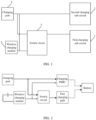
FIG. 1 is a first structural diagram of a charging control circuit according to an embodiment of this disclosure; -
FIG. 2 is a functional block diagram of a charging system according to an embodiment of this disclosure; -
FIG. 3 is a second structural diagram of a charging control circuit according to an embodiment of this disclosure; -
FIG. 4 is a third structural diagram of a charging control circuit according to an embodiment of this disclosure; -
FIG. 5 is a flowchart of a control method according to an embodiment of this disclosure; and -
FIG. 6 is a structural diagram of a terminal device according to an embodiment of this disclosure. - The following clearly and completely describes the technical solutions in the embodiments of this disclosure with reference to the accompanying drawings in the embodiments of this disclosure. Apparently, the described embodiments are some rather than all of the embodiments of this disclosure. All other embodiments obtained by a person of ordinary skill in the art based on the embodiments of this disclosure without creative efforts shall fall within the protection scope of this disclosure.
- Refer to
FIG. 1 , which is a structural diagram of a charging control circuit according to an embodiment of this disclosure. As shown inFIG. 1 , the charging control circuit includes afirst charging sub-circuit 1 and asecond charging sub-circuit 2, the charging efficiency of thefirst charging sub-circuit 1 being higher than the charging efficiency of thesecond charging sub-circuit 2, and the charging control circuit further includes aswitch circuit 3, where a first contact of theswitch circuit 3 is connected to acharging port 4, a second contact of theswitch circuit 3 is connected to an output terminal of a wireless charging module 5, and a third contact of theswitch circuit 3 is connected to an input terminal of thefirst charging sub-circuit 1; and in a case of a wireless charging operation, the first contact and the third contact disconnect from each other and the second contact and the third contact conductively connect to each other. - In this embodiment, the
first charging sub-circuit 1 may be a fast charging circuit, and thesecond charging sub-circuit 2 may be a charging power management integrated circuit (Power Management IC, PMIC). Since the first contact and the third contact disconnect from each other and the second contact and the third contact conductively connect to each other in the case of a wireless charging operation, thefirst charging sub-circuit 1 with higher charging efficiency of the terminal device is used for the wireless charging, thus improving the efficiency of charging a terminal device wirelessly. - In this embodiment, during a wireless charging operation using the
first charging sub-circuit 1, the wireless charging module 5 can output a high voltage, allowing smaller loss of an entire charging system in charging the terminal device wirelessly. This can increase the charging speed of the terminal device and reduce the temperature rise in charging, providing better user experience. In addition, when a wired charger is connected, the charging mode can automatically switch to wired charging, which allows higher charging speed. - Refer to
FIG. 2 , which is a functional block diagram of a charging system according to an embodiment of this disclosure. InFIG. 2 , a wired charging circuit (in the case of constant-current charging) includes a charging port, a switch circuit, a fast charging circuit, and a battery in order. A wired charging circuit (in the case of trickle charging, constant-voltage charging, and charging cutoff) includes the charging port, a charging PMIC, and the battery in order. A wireless charging circuit (in the case of constant-current charging) includes an inductor and capacitor, a wireless charging module, the switch circuit, the fast charging circuit, and the battery in order. A wireless charging circuit (in the case of trickle charging, constant-voltage charging, and charging cutoff) includes the inductor and capacitor, the wireless charging module, the charging PMIC, and the battery in order. Wherein - Trickle charging, constant-current charging, constant-voltage charging, and charging cutoff are four charging stages of (lithium-ion or lithium polymer) batteries. The charging PMIC and fast charging circuit are wired charging circuits of a charger, which are shared with wireless charging. During wireless charging, if a charger is connected to the charging port, the charging circuit automatically switches to a wired charging circuit.
- Optionally, the
switch circuit 3 includes a first sub-circuit and a second sub-circuit; - a first terminal of the first sub-circuit is connected to the first contact, and a second terminal of the first sub-circuit is connected to the third contact;
- a first terminal of the second sub-circuit is connected to the second contact, and a second terminal of the second sub-circuit is connected to the third contact; and
- in the case of a wireless charging operation, the first sub-circuit is disconnected and the second sub-circuit is conductive.
- In this implementation, the first sub-circuit and the second sub-circuit may be formed, for example, by a transistor, or by a diode and a transistor together, or by a MOS transistor and a diode, which is not limited in this embodiment.
- In this implementation, in the case of a wireless charging operation, the first sub-circuit is disconnected and the second sub-circuit is conductive. Thus, the first charging sub-circuit that has higher charging efficiency can be used for charging, improving the efficiency of charging a terminal device wirelessly.
- Optionally, the first sub-circuit includes a first NMOS transistor, a second NMOS transistor, a first diode, and a second diode;
- a drain of the first NMOS transistor is connected to the first contact, and a source of the first NMOS transistor is connected to a source of the second NMOS transistor;
- a drain of the second NMOS transistor is connected to the third contact;
- an anode of the first diode is connected to the source of the first NMOS transistor, and a cathode of the first diode is connected to the drain of the first NMOS transistor;
- an anode of the second diode is connected to the source of the second NMOS transistor, and a cathode of the second diode is connected to the drain of the second NMOS transistor; and
- a gate of the first NMOS transistor and a gate of the second NMOS transistor are both connected to a first control terminal.
- In this implementation, the first control terminal may be a control terminal inside the
switch circuit 3 or a control terminal outside theswitch circuit 3, which is not limited in this embodiment. As the first sub-circuit includes the first NMOS transistor and the second NMOS transistor, and the gate of the first NMOS transistor and the gate of the second NMOS transistor are both connected to the first control terminal, only one signal is required to control both the first NMOS transistor and the second NMOS transistor to be on or off, making it easier to control the circuit. - For example, when the first control terminal sends a first signal, the first NMOS transistor and the second NMOS transistor may be turned on, and when the first control terminal sends a second signal, the first NMOS transistor and the second NMOS transistor may be turned off, thus facilitating the ease of control. In the case of a wireless charging operation, the first control terminal sends the second signal, and the first NMOS transistor and the second NMOS transistor are both off, so that the second sub-circuit is not affected. In addition, the second sub-circuit may be turned on so that the first charging sub-circuit that has higher charging efficiency is used for charging, improving the efficiency of charging a terminal device wirelessly.
- Optionally, the second sub-circuit includes a third NMOS transistor, a fourth NMOS transistor, a third diode, and a fourth diode;
- a drain of the third NMOS transistor is connected to the second contact, and a source of the third NMOS transistor is connected to a source of the fourth NMOS transistor;
- a drain of the fourth NMOS transistor is connected to the third contact;
- an anode of the third diode is connected to the source of the third NMOS transistor, and a cathode of the third diode is connected to the drain of the third NMOS transistor;
- an anode of the fourth diode is connected to the source of the fourth NMOS transistor, and a cathode of the fourth diode is connected to the drain of the fourth NMOS transistor; and
- a gate of the third NMOS transistor and a gate of the fourth NMOS transistor are both connected to a second control terminal.
- In this implementation, the second control terminal may be a control terminal inside the
switch circuit 3 or a control terminal outside theswitch circuit 3, which is not limited in this embodiment. As the second sub-circuit includes the third NMOS transistor and the fourth NMOS transistor, and the gate of the third NMOS transistor and the gate of the fourth NMOS transistor are both connected to the second control terminal, only one signal is required to control both the third NMOS transistor and the fourth NMOS transistor to be on or off, making it easier to control the circuit. - For example, when the second control terminal sends a third signal, the third NMOS transistor and the fourth NMOS transistor may be turned on, and when the second control sends a fourth signal, the third NMOS transistor and the fourth NMOS transistor may be turned off, thus facilitating the ease of control. In the case of a wireless charging operation, the second control terminal sends the third signal and the third NMOS transistor and the fourth NMOS transistor are both on, so that the first charging sub-circuit that has higher charging efficiency is used for charging, improving the efficiency of charging a terminal device wirelessly. In addition, the first sub-circuit may be turned off in this case, avoiding impact of the first sub-circuit on the second sub-circuit.
- To better understand structures of the first sub-circuit, the second sub-circuit, and the entire charging control circuit, refer to
FIG. 3 and FIG. 4 , which are both structural diagrams of the charging control circuit provided in the embodiments of this disclosure. - First, as shown in
FIG. 3 , the first chargingsub-circuit 1 is a charging PMIC, and thesecond charging sub-circuit 2 is a fast charging circuit. The wireless charging module 5 integrates the circuit of a rectifier module which receives an alternate current signal from a transmitter and rectifies the alternate current signal to a direct current output voltage VINB that serves as an input voltage of the charging chip (charging PMIC or fast charging circuit). The wireless charging module 5 integrates circuits of two communication modules, which are an amplitude shift keying (Amplitude Shift Keying, ASK) communication module and a frequency shift keying (Frequency Shift Keying, FSK) communication module. The ASK communication module is responsible for modulating a communication signal of a receiver into a carrier signal, and sends the carrier signal to a transmitter device; the FSK communication module is responsible for receiving a communication signal sent from the transmitter and communicating with the system after demodulating that communication signal. The wireless charging module 5 also integrates circuits of protection mechanism modules (overvoltage and temperature) and others. - The
switch circuit 3 provides a low-impedance path for charging. The VINB path is used by default, and when a charger is connected to the charging port, a VINApath takes over automatically. - As shown in
FIG. 3 , the fast charging circuit is a half-voltage circuit. Internally, a single half-voltage device typically incorporates four NMOS transistors to function as its switch, which are Q1, Q3, Q2, and Q4 shown inFIG. 3 , and capacitor Cfly and capacitor Cout are connected in parallel. An input voltage is Vbus, a battery output voltage is VBAT, and a voltage across two terminals of the capacitor Cfly is Vcfly. When the circuit is working, on/off states of the transistors are controlled so as to charge or discharge the capacitor Cfly. The duty cycle of the switch is controlled to be 50%, making Vout=Vin/2, so that voltage is halved and current is doubled. - The charging PMIC is a high-efficiency charging IC which controls and manages charging parameters of the battery. VBAT is a pack of lithium-ion battery cells or a lithium polymer battery pack.
- refer to
FIG. 4 , where the first chargingsub-circuit 1 is a charging PMIC, and thesecond charging sub-circuit 2 is a fast charging circuit.FIG. 4 is different fromFIG. 3 in that the fast charging circuit is a direct charging equivalent circuit, where a direct charging switch used is typically implemented by two discrete N MOSFETs or an integrated IC (similar to discrete N MOSFETs). When the switch is on, a charger charges the battery VBAT directly. - The charging control circuit in the embodiments of this disclosure includes the first charging
sub-circuit 1 and thesecond charging sub-circuit 2, the charging efficiency of the first chargingsub-circuit 1 being higher than the charging efficiency of thesecond charging sub-circuit 2, and the charging control circuit further includes theswitch circuit 3; the first contact of theswitch circuit 3 is connected to the chargingport 4, the second contact of theswitch circuit 3 is connected to the output terminal of the wireless charging module 5, and the third contact of theswitch circuit 3 is connected to the input terminal of the first chargingsub-circuit 1; and in a case of a wireless charging operation, the first contact and the third contact disconnect from each other and the second contact and the third contact conductively connect to each other. Thus, the first charging sub-circuit that has higher charging efficiency can be used for charging in the case of a wireless charging operation, improving the efficiency of charging a terminal device wirelessly. - An embodiment of this disclosure further provides a terminal device that includes the foregoing charging control circuit.
- In this embodiment, the terminal device may be a mobile phone, a tablet personal computer (Tablet Personal Computer), a laptop computer (Laptop Computer), a personal digital assistant (personal digital assistant, PDA), a mobile internet device (Mobile Internet Device, MID), a wearable device (Wearable Device), or the like.
-
FIG. 5 is a flowchart of a control method according to an embodiment of this disclosure, where the method is applied to the foregoing terminal device. As shown inFIG. 5 , the control method includes the following steps. -
Step 501. Control, in a case of a wireless charging operation, the first contact and third contact of the switch circuit to disconnect from each other and the second contact and third contact of the switch circuit to conductively connect to each other. - In this embodiment, in the case of a wireless charging operation, the first contact and third contact of the switch circuit are controlled to disconnect from each other and the second contact and third contact of the switch circuit are controlled to conductively connect to each other. Thus, the first charging sub-circuit that has higher charging efficiency can be used for charging, improving the efficiency of charging the terminal device wirelessly.
- Optionally, the controlling the first contact and third contact of the switch circuit to disconnect from each other and the second contact and third contact of the switch circuit to conductively connect to each other includes:
in a case that a battery voltage is higher than a predetermined threshold voltage or that a battery temperature is lower than a predetermined threshold temperature, controlling the first contact and third contact of the switch circuit to disconnect from each other and the second contact and third contact of the switch circuit to conductively connect to each other. - In this implementation, in the case that the battery voltage is higher than the predetermined threshold voltage or that the battery temperature is lower than the predetermined threshold temperature, the first contact and third contact of the switch circuit are controlled to disconnect from each other and the second contact and third contact of the switch circuit are controlled to conductively connect to each other. Thus, a finer control process is possible by using the battery voltage or battery temperature as a judgment criterion.
- Optionally, the method further includes:
in a case that the battery voltage is lower than or equal to the predetermined threshold voltage and that the battery temperature is higher than or equal to the predetermined threshold temperature, performing wireless charging by using the second charging sub-circuit. - In this implementation, the case that the battery voltage is lower than or equal to the predetermined threshold voltage and that the battery temperature is higher than or equal to the predetermined threshold temperature does not conform to a fast charging condition, in this case, the second charging sub-circuit can be used for wireless charging, where the second charging sub-circuit may be a charging PMIC. Thus, the wireless charging process is safer.
- Optionally, before the controlling, in a case of a wireless charging operation, the first contact and third contact of the switch circuit to disconnect from each other and the second contact and third contact of the switch circuit to conductively connect to each other, the method further includes:
- sending a high-voltage charging request to a charger; and
- the controlling, in a case of a wireless charging operation, the first contact and third contact of the switch circuit to disconnect from each other and the second contact and third contact of the switch circuit to conductively connect to each other includes:
in a case of a wireless charging operation and successful request, controlling the first contact and third contact of the switch circuit to disconnect from each other and the second contact and third contact of the switch circuit to conductively connect to each other. - In this implementation, the charger is a wireless charger, and the high-voltage charging request may contain a requested high-voltage range. In the case of a wireless charging operation and successful request, the first contact and third contact of the switch circuit are controlled to disconnect from each other and the second contact and third contact of the switch circuit are controlled to conductively connect to each other. Successful request means that the wireless charger is able to provide a high voltage, in which case the first charging sub-circuit that has higher charging efficiency can be used for charging, improving the efficiency of charging the terminal device wirelessly.
- Optionally, after the sending a high-voltage charging request to a charger, the method further includes:
in a case of a wireless charging operation and unsuccessful request, performing wireless charging by using the second charging sub-circuit. - In this implementation, in the case of a wireless charging operation and unsuccessful request, the second charging sub-circuit is used for wireless charging. In this case, the wireless charger may not be able to output a high voltage in the requested range, and the charging PMIC may be used for charging.
- Optionally, after the controlling, in a case of a wireless charging operation, the first contact and third contact of the switch circuit to disconnect from each other and the second contact and third contact of the switch circuit to conductively connect to each other, the method further includes:
in a case that a wired charger is connected, controlling the first contact and third contact of the switch circuit to conductively connect to each other and the second contact and third contact of the switch circuit to disconnect from each other. - In this implementation, in the case that a wireless charger is connected, the first contact and third contact of the switch circuit are controlled to conductively connect to each other and the second contact and third contact of the switch circuit are controlled to disconnect from each other. The charging mode automatically switches to wired charging, which allows higher charging speed and less temperature rise.
- It should be noted that the foregoing implementations may be implemented separately or in combination with each other, which is not limited in the embodiments of this disclosure. For example, charging is not performed in a case of unsuccessful handshake between the terminal device and the wireless charger. In a case of successful handshake between the terminal device and the wireless charger, if a fast charging condition (constant-current charging stage of the battery, for example, when the battery voltage Vbat is higher than a predetermined value V1 or when the battery temperature T is lower than a predetermined value t1) is satisfied, a high-voltage mode is requested of the charger for wireless charging. After the charger outputs a high voltage, the terminal device uses the fast charging circuit for charging. If the fast charging condition (trickle charging or constant-voltage charging stage of the battery) is not satisfied, the charger is unable to output a high voltage in the requested range, and the charging PMIC path is used for charging.
- According to the control method in the embodiments of this disclosure, in the case of a wireless charging operation, the first contact and third contact of the switch circuit are controlled to disconnect from each other and the second contact and third contact of the switch circuit are controlled to conductively connect to each other. Thus, the first charging sub-circuit that has higher charging efficiency can be used for charging in the case of a wireless charging operation, improving the efficiency of charging the terminal device wirelessly.
- Referring to
FIG. 6, FIG. 6 is a schematic diagram of a hardware structure of a terminal device that implements the embodiments of this disclosure. Theterminal device 600 includes but is not limited to components such as aradio frequency unit 601, anetwork module 602, anaudio output unit 603, aninput unit 604, asensor 605, adisplay unit 606, auser input unit 607, aninterface unit 608, amemory 609, aprocessor 610, and apower supply 611. A person skilled in the art may understand that the structure of the terminal device shown inFIG. 6 does not constitute any limitation on the terminal device. The terminal device may include more or fewer components than shown in the figure, or have some of the components combined or have the components arranged differently. In this embodiment of this disclosure, the terminal device includes but is not limited to a mobile phone, a tablet computer, a laptop computer, a palmtop computer, an in-vehicle terminal, a wearable device, a pedometer, and the like. - The
processor 610 may be configured to control, in a case of a wireless charging operation, a first contact and a third contact that are of a switch circuit to disconnect from each other and a second contact and the third contact that are of the switch circuit to conductively connect to each other. Thus, a first charging sub-circuit that has higher charging efficiency can be used for charging in the case of a wireless charging operation, improving the efficiency of charging the terminal device wirelessly. - Optionally, the
processor 610 is further configured to, in a case that a battery voltage is higher than a predetermined threshold voltage or that a battery temperature is lower than a predetermined threshold temperature, control the first contact and third contact of the switch circuit to disconnect from each other and the second contact and third contact of the switch circuit to conductively connect to each other. - Optionally, the
processor 610 is further configured to, in a case that the battery voltage is lower than or equal to the predetermined threshold voltage and that the battery temperature is higher than or equal to the predetermined threshold temperature, control wireless charging to be performed by using the second charging sub-circuit. - Optionally, the
processor 610 is further configured to send a high-voltage charging request to a charger; and in a case of a wireless charging operation and successful request, control the first contact and third contact of the switch circuit to disconnect from each other and the second contact and third contact of the switch circuit to conductively connect to each other. - Optionally, the
processor 610 is further configured to, in a case of a wireless charging operation and unsuccessful request, control wireless charging to be performed by using the second charging sub-circuit. - Optionally, the
processor 610 is further configured to, in a case that a wired charger is connected, control the first contact and third contact of the switch circuit to conductively connect to each other and the second contact and third contact of the switch circuit to disconnect from each other. - It should be understood that in this embodiment of this disclosure, the
radio frequency unit 601 may be configured to receive/send information, or to receive/send a signal in a call process, and specifically, after receiving downlink data from a base station, send the downlink data to theprocessor 610 for processing; and send uplink data to the base station. Generally, theradio frequency unit 601 includes but is not limited to an antenna, at least one amplifier, a transceiver, a coupler, a low noise amplifier, a duplexer, and the like. In addition, theradio frequency unit 601 may further communicate with a network and another device through a wireless communications system. - The terminal device provides wireless broadband internet access for a user by using the
network module 602, for example, helps the user send and receive e-mails, browse web pages, or access streaming media. - The
audio output unit 603 may convert audio data received by theradio frequency unit 601 or thenetwork module 602 or stored in thememory 609 into an audio signal and output the audio signal as a sound. In addition, theaudio output unit 603 may further provide an audio output (for example, a call signal received sound or a message received sound) related to a specific function performed by theterminal device 600. Theaudio output unit 603 includes a speaker, a buzzer, a telephone receiver, and the like. - The
input unit 604 is configured to receive an audio or video signal. Theinput unit 604 may include a graphics processing unit (Graphics Processing Unit, GPU) 6041 and amicrophone 6042, and thegraphics processing unit 6041 processes image data of a still picture or a video obtained by an image capture apparatus (for example, a camera) in an image capture mode or a video capture mode. A processed image frame may be displayed on thedisplay unit 606. An image frame processed by thegraphics processing unit 6041 may be stored in the memory 609 (or other storage media) or sent by theradio frequency unit 601 or thenetwork module 602. Themicrophone 6042 can receive a sound and can process the sound into audio data. The processed audio data can be converted into a format that can be sent to a mobile communication base station through theradio frequency unit 601 in a telephone call mode, for outputting. - The
terminal device 600 further includes at least onesensor 605, for example, an optical sensor, a motion sensor, and other sensors. Specifically, the optical sensor includes an ambient light sensor and a proximity sensor. The ambient light sensor may adjust luminance of adisplay panel 6061 based on brightness of ambient light. The proximity sensor may turn off backlight and/or thedisplay panel 6061 when theterminal device 600 moves to an ear. As a type of motion sensor, an accelerometer sensor can detect magnitudes of accelerations in all directions (typically three axes), can detect the magnitude and direction of gravity when the mobile phone is in a static state, and can be applied to mobile phone posture recognition (such as screen switching between portrait and landscape, related games, and magnetometer posture calibration), functions related to vibration recognition (such as pedometer and tapping), and the like. Thesensor 605 may also include a fingerprint sensor, a pressure sensor, an iris sensor, a molecular sensor, a gyroscope, a barometer, a hygrometer, a thermometer, an infrared sensor, and the like. Details are not described herein. - The
display unit 606 is configured to display information input by the user or information provided for the user. Thedisplay unit 606 may include adisplay panel 6061, and thedisplay panel 6061 may be configured in the form of a liquid crystal display (Liquid Crystal Display, LCD), an organic light-emitting diode (Organic Light-Emitting Diode, OLED), or the like. - The
user input unit 607 may be configured to receive input digit or character information, and generate a key signal input related to user setting and function control of the terminal device. Specifically, theuser input unit 607 includes atouch panel 6071 andother input devices 6072. Thetouch panel 6071, also referred to as a touchscreen, may capture a touch operation performed by a user on or near the touch panel (for example, an operation performed by the user on thetouch panel 6071 or near thetouch panel 6071 by using any appropriate object or accessory such as a finger or a stylus). Thetouch panel 6071 may include two parts: a touch detection apparatus and a touch controller. The touch detection apparatus detects a touch direction of the user, detects a signal brought by a touch operation, and transmits the signal to the touch controller. The touch controller receives touch information from the touch detection apparatus, converts the touch information to touchpoint coordinates, and sends the touchpoint coordinates to theprocessor 610, and receives and executes a command sent by theprocessor 610. In addition, thetouch panel 6071 may be implemented in a plurality of forms, for example, as a resistive, capacitive, infrared, or surface acoustic wave touch panel. Theuser input unit 607 may further includeother input devices 6072 in addition to thetouch panel 6071. Specifically, theother input devices 6072 may include but are not limited to a physical keyboard, a function key (such as a volume control key or a power on/off key), a trackball, a mouse, a joystick, and the like. Details are not described herein. - Further, the
touch panel 6071 may cover thedisplay panel 6061. After detecting a touch operation on or near thetouch panel 6071, thetouch panel 6071 transmits information about the touch operation to theprocessor 610 for theprocessor 610 to determine a type of the touch event, and then theprocessor 610 provides a corresponding visual output on thedisplay panel 6061 based on the type of the touch event. Although thetouch panel 6071 and thedisplay panel 6061 are used as two independent components to implement input and output functions of the terminal device inFIG. 6 , thetouch panel 6071 and thedisplay panel 6061 may be integrated to implement the input and output functions of the terminal device in some embodiments. This is not specifically limited herein. - The
interface unit 608 is an interface for connecting an external apparatus to theterminal device 600. For example, the external apparatus may include a wired or wireless headphone port, an external power (or battery charger) port, a wired or wireless data port, a memory card port, a port for connecting an apparatus provided with a recognition module, an audio input/output (I/O) port, a video I/O port, an earphone port, and the like. Theinterface unit 608 may be configured to receive an input (for example, data information or power) from the external apparatus, and transmit the received input to one or more components in theterminal device 600, or may be configured to transmit data between theterminal device 600 and the external apparatus. - The
memory 609 may be configured to store software programs and various data. Thememory 609 may mainly include a program storage area and a data storage area. The program storage area may store an operating system, an application program required for at least one function (such as a sound play function and an image play function), and the like. The data storage area may store data created based on use of the mobile phone (such as audio data and a phone book), and the like. In addition, thememory 609 may include a high-speed random access memory, and may further include a non-volatile memory, for example, at least one magnetic disk storage device, a flash memory device, or other volatile solid-state storage devices. - The
processor 610 is a control center of the terminal device. Theprocessor 610 uses various interfaces and lines to connect all parts of the entire terminal device, and performs various functions and data processing of the terminal device by running or executing the software programs and/or modules stored in thememory 609 and calling the data stored in thememory 609, thereby performing overall monitoring on the terminal device. Theprocessor 610 may include one or more processing units. Preferably, theprocessor 610 may integrate an application processor and a modem processor. The application processor mainly processes the operating system, a user interface, an application program, and the like. The modem processor mainly processes wireless communication. It may be understood that the modem processor may alternatively not be integrated into theprocessor 610. - The
terminal device 600 may further include the power supply 611 (such as a battery) that supplies power to the components. Preferably, thepower supply 611 may be logically connected to theprocessor 610 via a power management system, so that functions such as charge and discharge management and power consumption management are implemented via the power management system. - In addition, the
terminal device 600 includes some functional modules that are not illustrated. Details are not described herein. - Optionally, an embodiment of this disclosure further provides a terminal device, including a
processor 610, amemory 609, and a computer program stored in thememory 609 and capable of being run on theprocessor 610. When the computer program is executed by theprocessor 610, the processes in the foregoing embodiments of the control method are implemented, with the same technical effect achieved. To avoid repetition, details are not described herein again. - An embodiment of this disclosure further provides a computer-readable storage medium, where the computer-readable storage medium stores a computer program, and when the computer program is executed by a processor, the processes in the foregoing embodiments of the control method are implemented, with the same technical effects. To avoid repetition, details are not described herein again. The computer-readable storage medium is, for example, a read-only memory (Read-Only Memory, ROM), a random access memory (Random Access Memory, RAM), a magnetic disk, or an optical disc.
- It should be noted that, in this specification, the terms "include", "comprise", and any of their variants are intended to cover a non-exclusive inclusion, such that a process, method, article, or apparatus that includes a list of elements not only includes those elements but also includes other elements that are not expressly listed, or further includes elements inherent to such process, method, article, or apparatus. In absence of more constraints, an element preceded by "includes a..." does not preclude the existence of other identical elements in the process, method, article, or apparatus that includes that element.
- According to the description of the foregoing implementations, a person skilled in the art can clearly understand that the method in the foregoing embodiments may be implemented by software on a necessary universal hardware platform or by hardware only. In most cases, the former is a more preferred implementation. Based on such an understanding, the technical solutions of this disclosure essentially, or the part contributing to the prior art may be implemented in a form of a software product. The computer software product is stored in a storage medium (for example, a ROM/RAM, a magnetic disk, or an optical disc), and includes several instructions for instructing a terminal (which may be a mobile phone, a computer, a server, an air conditioner, a network device, or the like) to perform the method described in the embodiments of this disclosure.
- The embodiments of this disclosure have been described above with reference to the accompanying drawings, but this disclosure is not limited to the foregoing specific implementations. These implementations are only illustrative rather than restrictive. Inspired by this disclosure, a person of ordinary skill in the art can still derive many variations without departing from the essence of this disclosure and the protection scope of the claims. All such variations shall fall within the protection of this disclosure.
Claims (13)
- A charging control circuit, wherein the charging control circuit comprises a first charging sub-circuit (1) and a second charging sub-circuit (2), and the charging control circuit further comprises a switch circuit (3),a first contact of the switch circuit (3) is connected to a charging port (4) of the charging control circuit, a second contact of the switch circuit (3) is connected to an output terminal of a wireless charging module (5) of the charging control circuit, and a third contact of the switch circuit (3) is connected to an input terminal of the first charging sub-circuit (1);characterized in thata charging efficiency of the first charging sub-circuit (1) is higher than a charging efficiency of the second charging sub-circuit (2),
andin a case of a wireless charging operation, the first contact and the third contact are configured to disconnect from each other and the second contact and the third contact are configured to conductively connect to each other. - The charging control circuit according to claim 1, wherein the switch circuit (3) further comprises a first sub-circuit and a second sub-circuit;a first terminal of the first sub-circuit is connected to the first contact, and a second terminal of the first sub-circuit is connected to the third contact;a first terminal of the second sub-circuit is connected to the second contact, and a second terminal of the second sub-circuit is connected to the third contact; andin the case of a wireless charging operation, the first sub-circuit is configured to be disconnected and the second sub-circuit is conductive.
- The charging control circuit according to claim 2, wherein the first sub-circuit comprises a first NMOS transistor, a second NMOS transistor, a first diode, and a second diode;a drain of the first NMOS transistor is connected to the first contact, and a source of the first NMOS transistor is connected to a source of the second NMOS transistor;a drain of the second NMOS transistor is connected to the third contact;an anode of the first diode is connected to the source of the first NMOS transistor, and a cathode of the first diode is connected to the drain of the first NMOS transistor;an anode of the second diode is connected to the source of the second NMOS transistor, and a cathode of the second diode is connected to the drain of the second NMOS transistor; anda gate of the first NMOS transistor and a gate of the second NMOS transistor are both connected to a first control terminal.
- The charging control circuit according to claim 2, wherein the second sub-circuit comprises a third NMOS transistor, a fourth NMOS transistor, a third diode, and a fourth diode;a drain of the third NMOS transistor is connected to the second contact, and a source of the third NMOS transistor is connected to a source of the fourth NMOS transistor;a drain of the fourth NMOS transistor is connected to the third contact;an anode of the third diode is connected to the source of the third NMOS transistor, and a cathode of the third diode is connected to the drain of the third NMOS transistor;an anode of the fourth diode is connected to the source of the fourth NMOS transistor, and a cathode of the fourth diode is connected to the drain of the fourth NMOS transistor; anda gate of the third NMOS transistor and a gate of the fourth NMOS transistor are both connected to a second control terminal.
- A terminal device, characterized in that comprising the charging control circuit according to any one of claims 1 to 4.
- A control method, applied to the terminal device according to claim 5, the method being characterized in that it comprises:
controlling (501), in a case of a wireless charging operation, the first contact and third contact of the switch circuit to disconnect from each other and the second contact and third contact of the switch circuit to conductively connect to each other. - The method according to claim 6, wherein the controlling (501) the first contact and third contact of the switch circuit to disconnect from each other and the second contact and third contact of the switch circuit to conductively connect to each other comprises:
in a case that a battery voltage is higher than a predetermined threshold voltage or that a battery temperature is lower than a predetermined threshold temperature, controlling the first contact and third contact of the switch circuit to disconnect from each other and the second contact and third contact of the switch circuit to conductively connect to each other. - The method according to claim 7, wherein the method further comprises:
in a case that the battery voltage is lower than or equal to the predetermined threshold voltage and that the battery temperature is higher than or equal to the predetermined threshold temperature, performing wireless charging by using the second charging sub-circuit. - The method according to claim 6, wherein before the controlling (501), in a case of a wireless charging operation, the first contact and third contact of the switch circuit to disconnect from each other and the second contact and third contact of the switch circuit to conductively connect to each other, the method further comprises:sending a high-voltage charging request to a charger; andthe controlling (501), in a case of a wireless charging operation, the first contact and third contact of the switch circuit to disconnect from each other and the second contact and third contact of the switch circuit to conductively connect to each other comprises:
in a case of a wireless charging operation and successful request, controlling the first contact and third contact of the switch circuit to disconnect from each other and the second contact and third contact of the switch circuit to conductively connect to each other. - The method according to claim 9, wherein after the sending a high-voltage charging request to a charger, the method further comprises:
in a case of a wireless charging operation and unsuccessful request, performing wireless charging by using the second charging sub-circuit. - The method according to claim 6, wherein after the controlling (501), in a case of a wireless charging operation, the first contact and third contact of the switch circuit to disconnect from each other and the second contact and third contact of the switch circuit to conductively connect to each other, the method further comprises:
in a case that a wired charger is connected, controlling the first contact and third contact of the switch circuit to conductively connect to each other and the second contact and third contact of the switch circuit to disconnect from each other. - A terminal device (600), comprising a processor (610), a memory (609), and a computer program stored in the memory (609) and capable of being run on the processor (610), characterized in that when the computer program is executed by the processor (610), the control method according to any one of claims 6 to 11 are implemented.
- A computer-readable storage medium, characterized in that the computer-readable storage medium stores a computer program, and when the computer program is executed by a processor, the control method according to any one of claims 6 to 11 are implemented.
Applications Claiming Priority (2)
| Application Number | Priority Date | Filing Date | Title |
|---|---|---|---|
| CN201910133245.4A CN109672254B (en) | 2019-02-22 | 2019-02-22 | Charging control circuit, terminal equipment and control method |
| PCT/CN2020/073201 WO2020168892A1 (en) | 2019-02-22 | 2020-01-20 | Charging control circuit, terminal device and control method |
Publications (3)
| Publication Number | Publication Date |
|---|---|
| EP3930138A1 EP3930138A1 (en) | 2021-12-29 |
| EP3930138A4 EP3930138A4 (en) | 2022-04-13 |
| EP3930138B1 true EP3930138B1 (en) | 2023-09-27 |
Family
ID=66152111
Family Applications (1)
| Application Number | Title | Priority Date | Filing Date |
|---|---|---|---|
| EP20758970.6A Active EP3930138B1 (en) | 2019-02-22 | 2020-01-20 | Charging control circuit, terminal device and control method |
Country Status (7)
| Country | Link |
|---|---|
| US (1) | US20210384749A1 (en) |
| EP (1) | EP3930138B1 (en) |
| KR (1) | KR102614481B1 (en) |
| CN (1) | CN109672254B (en) |
| BR (1) | BR112021016498A2 (en) |
| ES (1) | ES2963471T3 (en) |
| WO (1) | WO2020168892A1 (en) |
Families Citing this family (7)
| Publication number | Priority date | Publication date | Assignee | Title |
|---|---|---|---|---|
| JP6812537B2 (en) * | 2017-04-07 | 2021-01-13 | オッポ広東移動通信有限公司Guangdong Oppo Mobile Telecommunications Corp., Ltd. | Wireless charging system, device, method and equipment to be charged |
| US11498437B2 (en) * | 2018-11-05 | 2022-11-15 | Mahle International Gmbh | Inductive charging system with modular underground protection |
| CN109672254B (en) * | 2019-02-22 | 2021-01-29 | 维沃移动通信有限公司 | Charging control circuit, terminal equipment and control method |
| CN112003357B (en) * | 2020-08-25 | 2022-11-22 | 中车株洲电力机车研究所有限公司 | Circuit control method based on solid-state switch |
| CN112134337A (en) * | 2020-09-23 | 2020-12-25 | 维沃移动通信有限公司 | Power adapter, terminal device, electronic device and charging control method thereof |
| CN113241835B (en) * | 2021-06-25 | 2024-05-03 | 维沃移动通信有限公司 | Charging module, electronic equipment and charging control method |
| WO2023230808A1 (en) * | 2022-05-31 | 2023-12-07 | Renesas Electronics America Inc. | Multi path battery charger |
Family Cites Families (8)
| Publication number | Priority date | Publication date | Assignee | Title |
|---|---|---|---|---|
| KR101727495B1 (en) * | 2010-12-28 | 2017-05-02 | 엘지전자 주식회사 | Mobile terminal |
| US9583970B2 (en) * | 2015-05-15 | 2017-02-28 | National Yunlin University Of Science And Technology | Wireless power transfer and rapid charging system and method with maximum power tracking |
| CN206117963U (en) * | 2016-10-17 | 2017-04-19 | 广州斐诺电子科技有限公司 | Earphone with wireless function of charging |
| US10305312B2 (en) * | 2016-11-08 | 2019-05-28 | Lenovo (Singapore) Pte. Ltd. | Supplemental power system for battery powered device |
| CN106654424A (en) * | 2016-11-30 | 2017-05-10 | 努比亚技术有限公司 | Charging method and terminal |
| EP3343727B1 (en) * | 2016-12-30 | 2021-01-20 | HTC Corporation | User privacy protection in wireless charging system |
| CN108879841B (en) * | 2018-06-28 | 2020-10-16 | 努比亚技术有限公司 | Parallel charging circuit and mobile terminal |
| CN109672254B (en) * | 2019-02-22 | 2021-01-29 | 维沃移动通信有限公司 | Charging control circuit, terminal equipment and control method |
-
2019
- 2019-02-22 CN CN201910133245.4A patent/CN109672254B/en active Active
-
2020
- 2020-01-20 EP EP20758970.6A patent/EP3930138B1/en active Active
- 2020-01-20 WO PCT/CN2020/073201 patent/WO2020168892A1/en unknown
- 2020-01-20 BR BR112021016498-7A patent/BR112021016498A2/en unknown
- 2020-01-20 KR KR1020217028539A patent/KR102614481B1/en active IP Right Grant
- 2020-01-20 ES ES20758970T patent/ES2963471T3/en active Active
-
2021
- 2021-08-20 US US17/407,303 patent/US20210384749A1/en active Pending
Also Published As
| Publication number | Publication date |
|---|---|
| KR102614481B1 (en) | 2023-12-14 |
| US20210384749A1 (en) | 2021-12-09 |
| CN109672254A (en) | 2019-04-23 |
| BR112021016498A2 (en) | 2021-10-26 |
| KR20210120103A (en) | 2021-10-06 |
| EP3930138A1 (en) | 2021-12-29 |
| CN109672254B (en) | 2021-01-29 |
| WO2020168892A1 (en) | 2020-08-27 |
| ES2963471T3 (en) | 2024-03-27 |
| EP3930138A4 (en) | 2022-04-13 |
Similar Documents
| Publication | Publication Date | Title |
|---|---|---|
| EP3930138B1 (en) | Charging control circuit, terminal device and control method | |
| US11336105B2 (en) | Multi-battery charging and discharging device and mobile terminal | |
| CN107546808B (en) | Charging identification circuit, identification method and terminal equipment | |
| CN108494030B (en) | Wireless charging method, terminal and transmitting terminal equipment | |
| CN111092621B (en) | Radio frequency circuit, control method and electronic equipment | |
| US20210391753A1 (en) | Terminal and wireless charging control method | |
| CN107645189B (en) | Charging protection method and mobile terminal | |
| CN107834640B (en) | Charging method and terminal | |
| CN108879841B (en) | Parallel charging circuit and mobile terminal | |
| CN107785961B (en) | Series battery charging method, mobile terminal and computer readable medium | |
| CN107516917A (en) | Charge control method, terminal, intelligent charge equipment and computer-readable storage medium | |
| EP4114034A1 (en) | Audio-playing apparatus, audio-playing method, and electronic device | |
| CN109842872A (en) | Working mode control method, Bluetooth headset, terminal and computer storage medium | |
| US11375497B2 (en) | Power configuration method and terminal | |
| US20210320526A1 (en) | Wireless charging control method, circuit and terminal device | |
| CN109889942B (en) | Type-C patch cord, control method and terminal equipment | |
| US20220416557A1 (en) | Electronic device | |
| CN111463912A (en) | Electronic device and power supply control method | |
| CN111182215A (en) | Power supply device of separable camera module | |
| CN109980724B (en) | Method and device for charging double-screen mobile terminal, mobile terminal and storage medium | |
| CN107863795B (en) | Parallel battery module charging method, mobile terminal and computer readable storage medium | |
| CN107562167B (en) | Multi-path charging method, mobile terminal and computer-readable storage medium | |
| CN107591858B (en) | Charging method, terminal and computer readable storage medium | |
| CN110739742A (en) | Charging protection method, charging protection circuit, charging system and terminal | |
| CN211655786U (en) | Electronic equipment and portable power source |
Legal Events
| Date | Code | Title | Description |
|---|---|---|---|
| STAA | Information on the status of an ep patent application or granted ep patent |
Free format text: STATUS: THE INTERNATIONAL PUBLICATION HAS BEEN MADE |
|
| PUAI | Public reference made under article 153(3) epc to a published international application that has entered the european phase |
Free format text: ORIGINAL CODE: 0009012 |
|
| STAA | Information on the status of an ep patent application or granted ep patent |
Free format text: STATUS: REQUEST FOR EXAMINATION WAS MADE |
|
| 17P | Request for examination filed |
Effective date: 20210908 |
|
| AK | Designated contracting states |
Kind code of ref document: A1 Designated state(s): AL AT BE BG CH CY CZ DE DK EE ES FI FR GB GR HR HU IE IS IT LI LT LU LV MC MK MT NL NO PL PT RO RS SE SI SK SM TR |
|
| A4 | Supplementary search report drawn up and despatched |
Effective date: 20220314 |
|
| RIC1 | Information provided on ipc code assigned before grant |
Ipc: H02J 50/10 20160101ALI20220308BHEP Ipc: H02J 7/00 20060101AFI20220308BHEP |
|
| DAV | Request for validation of the european patent (deleted) | ||
| DAX | Request for extension of the european patent (deleted) | ||
| GRAP | Despatch of communication of intention to grant a patent |
Free format text: ORIGINAL CODE: EPIDOSNIGR1 |
|
| STAA | Information on the status of an ep patent application or granted ep patent |
Free format text: STATUS: GRANT OF PATENT IS INTENDED |
|
| INTG | Intention to grant announced |
Effective date: 20230420 |
|
| GRAS | Grant fee paid |
Free format text: ORIGINAL CODE: EPIDOSNIGR3 |
|
| GRAA | (expected) grant |
Free format text: ORIGINAL CODE: 0009210 |
|
| STAA | Information on the status of an ep patent application or granted ep patent |
Free format text: STATUS: THE PATENT HAS BEEN GRANTED |
|
| AK | Designated contracting states |
Kind code of ref document: B1 Designated state(s): AL AT BE BG CH CY CZ DE DK EE ES FI FR GB GR HR HU IE IS IT LI LT LU LV MC MK MT NL NO PL PT RO RS SE SI SK SM TR |
|
| REG | Reference to a national code |
Ref country code: GB Ref legal event code: FG4D |
|
| REG | Reference to a national code |
Ref country code: CH Ref legal event code: EP |
|
| REG | Reference to a national code |
Ref country code: DE Ref legal event code: R096 Ref document number: 602020018344 Country of ref document: DE |
|
| REG | Reference to a national code |
Ref country code: IE Ref legal event code: FG4D |
|
| REG | Reference to a national code |
Ref country code: NL Ref legal event code: FP |
|
| REG | Reference to a national code |
Ref country code: LT Ref legal event code: MG9D |
|
| PG25 | Lapsed in a contracting state [announced via postgrant information from national office to epo] |
Ref country code: GR Free format text: LAPSE BECAUSE OF FAILURE TO SUBMIT A TRANSLATION OF THE DESCRIPTION OR TO PAY THE FEE WITHIN THE PRESCRIBED TIME-LIMIT Effective date: 20231228 |
|
| PGFP | Annual fee paid to national office [announced via postgrant information from national office to epo] |
Ref country code: GB Payment date: 20231130 Year of fee payment: 5 |
|
| PG25 | Lapsed in a contracting state [announced via postgrant information from national office to epo] |
Ref country code: SE Free format text: LAPSE BECAUSE OF FAILURE TO SUBMIT A TRANSLATION OF THE DESCRIPTION OR TO PAY THE FEE WITHIN THE PRESCRIBED TIME-LIMIT Effective date: 20230927 Ref country code: RS Free format text: LAPSE BECAUSE OF FAILURE TO SUBMIT A TRANSLATION OF THE DESCRIPTION OR TO PAY THE FEE WITHIN THE PRESCRIBED TIME-LIMIT Effective date: 20230927 Ref country code: NO Free format text: LAPSE BECAUSE OF FAILURE TO SUBMIT A TRANSLATION OF THE DESCRIPTION OR TO PAY THE FEE WITHIN THE PRESCRIBED TIME-LIMIT Effective date: 20231227 Ref country code: LV Free format text: LAPSE BECAUSE OF FAILURE TO SUBMIT A TRANSLATION OF THE DESCRIPTION OR TO PAY THE FEE WITHIN THE PRESCRIBED TIME-LIMIT Effective date: 20230927 Ref country code: LT Free format text: LAPSE BECAUSE OF FAILURE TO SUBMIT A TRANSLATION OF THE DESCRIPTION OR TO PAY THE FEE WITHIN THE PRESCRIBED TIME-LIMIT Effective date: 20230927 Ref country code: HR Free format text: LAPSE BECAUSE OF FAILURE TO SUBMIT A TRANSLATION OF THE DESCRIPTION OR TO PAY THE FEE WITHIN THE PRESCRIBED TIME-LIMIT Effective date: 20230927 Ref country code: GR Free format text: LAPSE BECAUSE OF FAILURE TO SUBMIT A TRANSLATION OF THE DESCRIPTION OR TO PAY THE FEE WITHIN THE PRESCRIBED TIME-LIMIT Effective date: 20231228 Ref country code: FI Free format text: LAPSE BECAUSE OF FAILURE TO SUBMIT A TRANSLATION OF THE DESCRIPTION OR TO PAY THE FEE WITHIN THE PRESCRIBED TIME-LIMIT Effective date: 20230927 |
|
| PGFP | Annual fee paid to national office [announced via postgrant information from national office to epo] |
Ref country code: NL Payment date: 20231215 Year of fee payment: 5 Ref country code: FR Payment date: 20231212 Year of fee payment: 5 |
|
| REG | Reference to a national code |
Ref country code: AT Ref legal event code: MK05 Ref document number: 1616361 Country of ref document: AT Kind code of ref document: T Effective date: 20230927 |
|
| REG | Reference to a national code |
Ref country code: ES Ref legal event code: FG2A Ref document number: 2963471 Country of ref document: ES Kind code of ref document: T3 Effective date: 20240327 |
|
| PG25 | Lapsed in a contracting state [announced via postgrant information from national office to epo] |
Ref country code: IS Free format text: LAPSE BECAUSE OF FAILURE TO SUBMIT A TRANSLATION OF THE DESCRIPTION OR TO PAY THE FEE WITHIN THE PRESCRIBED TIME-LIMIT Effective date: 20240127 |
|
| PGFP | Annual fee paid to national office [announced via postgrant information from national office to epo] |
Ref country code: ES Payment date: 20240205 Year of fee payment: 5 |
|
| PG25 | Lapsed in a contracting state [announced via postgrant information from national office to epo] |
Ref country code: AT Free format text: LAPSE BECAUSE OF FAILURE TO SUBMIT A TRANSLATION OF THE DESCRIPTION OR TO PAY THE FEE WITHIN THE PRESCRIBED TIME-LIMIT Effective date: 20230927 |
|
| PG25 | Lapsed in a contracting state [announced via postgrant information from national office to epo] |
Ref country code: SM Free format text: LAPSE BECAUSE OF FAILURE TO SUBMIT A TRANSLATION OF THE DESCRIPTION OR TO PAY THE FEE WITHIN THE PRESCRIBED TIME-LIMIT Effective date: 20230927 Ref country code: RO Free format text: LAPSE BECAUSE OF FAILURE TO SUBMIT A TRANSLATION OF THE DESCRIPTION OR TO PAY THE FEE WITHIN THE PRESCRIBED TIME-LIMIT Effective date: 20230927 Ref country code: IS Free format text: LAPSE BECAUSE OF FAILURE TO SUBMIT A TRANSLATION OF THE DESCRIPTION OR TO PAY THE FEE WITHIN THE PRESCRIBED TIME-LIMIT Effective date: 20240127 Ref country code: EE Free format text: LAPSE BECAUSE OF FAILURE TO SUBMIT A TRANSLATION OF THE DESCRIPTION OR TO PAY THE FEE WITHIN THE PRESCRIBED TIME-LIMIT Effective date: 20230927 Ref country code: CZ Free format text: LAPSE BECAUSE OF FAILURE TO SUBMIT A TRANSLATION OF THE DESCRIPTION OR TO PAY THE FEE WITHIN THE PRESCRIBED TIME-LIMIT Effective date: 20230927 Ref country code: AT Free format text: LAPSE BECAUSE OF FAILURE TO SUBMIT A TRANSLATION OF THE DESCRIPTION OR TO PAY THE FEE WITHIN THE PRESCRIBED TIME-LIMIT Effective date: 20230927 Ref country code: SK Free format text: LAPSE BECAUSE OF FAILURE TO SUBMIT A TRANSLATION OF THE DESCRIPTION OR TO PAY THE FEE WITHIN THE PRESCRIBED TIME-LIMIT Effective date: 20230927 Ref country code: PT Free format text: LAPSE BECAUSE OF FAILURE TO SUBMIT A TRANSLATION OF THE DESCRIPTION OR TO PAY THE FEE WITHIN THE PRESCRIBED TIME-LIMIT Effective date: 20240129 |
|
| PGFP | Annual fee paid to national office [announced via postgrant information from national office to epo] |
Ref country code: DE Payment date: 20231205 Year of fee payment: 5 |