EP3896863B1 - Near-field measuring device - Google Patents
Near-field measuring device Download PDFInfo
- Publication number
- EP3896863B1 EP3896863B1 EP21165364.7A EP21165364A EP3896863B1 EP 3896863 B1 EP3896863 B1 EP 3896863B1 EP 21165364 A EP21165364 A EP 21165364A EP 3896863 B1 EP3896863 B1 EP 3896863B1
- Authority
- EP
- European Patent Office
- Prior art keywords
- field
- antenna
- field antenna
- capacitance
- tuning circuit
- Prior art date
- Legal status (The legal status is an assumption and is not a legal conclusion. Google has not performed a legal analysis and makes no representation as to the accuracy of the status listed.)
- Active
Links
- 238000005259 measurement Methods 0.000 claims description 30
- 238000004804 winding Methods 0.000 claims description 27
- 238000004891 communication Methods 0.000 claims description 25
- 230000001902 propagating effect Effects 0.000 claims description 16
- 230000004044 response Effects 0.000 claims description 15
- 230000008878 coupling Effects 0.000 claims description 8
- 238000010168 coupling process Methods 0.000 claims description 8
- 238000005859 coupling reaction Methods 0.000 claims description 8
- 230000008901 benefit Effects 0.000 description 8
- 230000005684 electric field Effects 0.000 description 6
- 230000006698 induction Effects 0.000 description 3
- 238000004519 manufacturing process Methods 0.000 description 3
- 238000000034 method Methods 0.000 description 3
- 230000005855 radiation Effects 0.000 description 3
- 230000035945 sensitivity Effects 0.000 description 3
- 229910000859 α-Fe Inorganic materials 0.000 description 3
- 239000003990 capacitor Substances 0.000 description 2
- 238000013461 design Methods 0.000 description 2
- 230000005672 electromagnetic field Effects 0.000 description 2
- 238000012544 monitoring process Methods 0.000 description 2
- 238000012545 processing Methods 0.000 description 2
- 230000009467 reduction Effects 0.000 description 2
- WQZGKKKJIJFFOK-GASJEMHNSA-N Glucose Natural products OC[C@H]1OC(O)[C@H](O)[C@@H](O)[C@@H]1O WQZGKKKJIJFFOK-GASJEMHNSA-N 0.000 description 1
- 230000005540 biological transmission Effects 0.000 description 1
- 230000000694 effects Effects 0.000 description 1
- 230000005674 electromagnetic induction Effects 0.000 description 1
- 239000008103 glucose Substances 0.000 description 1
- 230000003993 interaction Effects 0.000 description 1
- 239000000463 material Substances 0.000 description 1
- 229940127554 medical product Drugs 0.000 description 1
- 238000012986 modification Methods 0.000 description 1
- 230000004048 modification Effects 0.000 description 1
- 238000001228 spectrum Methods 0.000 description 1
- 238000012546 transfer Methods 0.000 description 1
Images


Classifications
-
- H04B5/22—
-
- H—ELECTRICITY
- H04—ELECTRIC COMMUNICATION TECHNIQUE
- H04B—TRANSMISSION
- H04B17/00—Monitoring; Testing
- H04B17/20—Monitoring; Testing of receivers
-
- H—ELECTRICITY
- H04—ELECTRIC COMMUNICATION TECHNIQUE
- H04W—WIRELESS COMMUNICATION NETWORKS
- H04W4/00—Services specially adapted for wireless communication networks; Facilities therefor
- H04W4/80—Services using short range communication, e.g. near-field communication [NFC], radio-frequency identification [RFID] or low energy communication
-
- H—ELECTRICITY
- H01—ELECTRIC ELEMENTS
- H01Q—ANTENNAS, i.e. RADIO AERIALS
- H01Q1/00—Details of, or arrangements associated with, antennas
- H01Q1/12—Supports; Mounting means
- H01Q1/22—Supports; Mounting means by structural association with other equipment or articles
-
- H—ELECTRICITY
- H01—ELECTRIC ELEMENTS
- H01Q—ANTENNAS, i.e. RADIO AERIALS
- H01Q1/00—Details of, or arrangements associated with, antennas
- H01Q1/27—Adaptation for use in or on movable bodies
- H01Q1/273—Adaptation for carrying or wearing by persons or animals
-
- H—ELECTRICITY
- H01—ELECTRIC ELEMENTS
- H01Q—ANTENNAS, i.e. RADIO AERIALS
- H01Q7/00—Loop antennas with a substantially uniform current distribution around the loop and having a directional radiation pattern in a plane perpendicular to the plane of the loop
-
- G—PHYSICS
- G01—MEASURING; TESTING
- G01R—MEASURING ELECTRIC VARIABLES; MEASURING MAGNETIC VARIABLES
- G01R29/00—Arrangements for measuring or indicating electric quantities not covered by groups G01R19/00 - G01R27/00
- G01R29/08—Measuring electromagnetic field characteristics
- G01R29/0864—Measuring electromagnetic field characteristics characterised by constructional or functional features
- G01R29/0878—Sensors; antennas; probes; detectors
Definitions
- the present specification relates to systems, methods, apparatuses, devices, articles of manufacture and instructions for near-field measurement.
- a near-field measuring device comprising: a near-field antenna; a tuning circuit galvanically coupled to the near-field antenna and configured to set a resonant frequency and/or a quality factor of the measuring device; and a current sensor inductively coupled to the near-field antenna and configured to generate a signal in response to a current flowing through the galvanic coupling between the near-field antenna and the tuning circuit; wherein the signal represents a measurement of non-propagating quasi-static near-field signals received by the near-field antenna.
- the current sensor is a transformer or a toroidal coil.
- the current sensor is configured to amplify the current flowing in the galvanic coupling.
- the tuning circuit includes a capacitance and a resistance.
- the near-field antenna includes a set of conductive surfaces configured to be responsive to an electric near-field signal; the conductive surfaces together form a capacitance; the tuning circuit capacitance is larger than the conductive surfaces capacitance such that a larger portion of the current flowing through near-field antenna flows through the tuning circuit capacitance; and the current sensor is inductively coupled in series with the tuning circuit capacitance and coupled in parallel with the tuning circuit resistance.
- the current sensor includes a primary winding and a secondary winding; wherein the primary winding is galvanically coupled to the near-field antenna; and wherein the secondary winding is inductively coupled to the primary winding, and galvanically coupled to the sensing element.
- the sensing element includes a resistance; the signal is a voltage; and the resistance is configured to generate the voltage in response to the current flowing through the primary winding.
- the sensing element includes a low noise amplifier; the signal is a voltage; and the low noise amplifier is configured to generate an amplified output signal in response to the current flowing through the primary winding.
- the sensing element is configured to be coupled to a measurement instrument; and the measurement instrument is configured to output either a magnetic near-field strength signal and/or an electric near-field strength signal in response to the current flowing through the primary winding.
- the sensing element is configured to be coupled to a baseband communications circuit; and the communications circuit is configured to output a communications signal in response to the current flowing through the primary winding.
- the tuning circuit includes a variable tuning capacitance bank configured to set a resonant frequency of the near-field antenna in response to a control line.
- the tuning circuit includes a variable tuning resistance bank configured to set a quality factor or bandwidth of the near-field antenna in response to a control line.
- the tuning circuit includes a fixed tuning capacitance configured to set a fixed resonant frequency of the near-field antenna and a fixed tuning resistance configured to set a fixed quality factor or bandwidth of the near-field antenna.
- the current flowing in the galvanic coupling between the near-field antenna and the tuning circuit is generated only by the non-propagating quasi-static near-field signals received by the near-field antenna.
- the near-field antenna is a near-field magnetic antenna responsive to non-propagating quasi-static near-field magnetic signals.
- the near-field antenna is a near-field electric antenna responsive to non-propagating quasi-static near-field electric signals.
- the near-field antenna is a near-field electromagnetic antenna responsive to non-propagating quasi-static near-field electric and magnetic signals.
- the near-field measuring device is configured to be capacitively coupled to an external conductive surface from which the measurement of non-propagating quasi-static near-field signals is to be made.
- the near-field measuring device is embedded in at least one of: a wearable device; a smart watch; a smartwatch housing, an earbud, a hearing aid, a medical device, an activity tracker, or a heart rate monitor.
- near-field interactions between a near-field device perhaps on a user's body, and other conductive surfaces and/or other wireless networked devices (e.g. Internet of Things (IoT) devices, wearables, earbuds, body area networks, gaming products and medical products like continuous glucose monitoring, etc.) based on near-field electromagnetic induction (NFEMI), where the transmitter and receiver are coupled by both magnetic (H) and electric (E) fields.
- IoT Internet of Things
- E electric
- An H-field antenna i.e. magnetic antenna
- Any E-field component from an H-field antenna is strongly reduced (e.g. -20 to -60 dB reduction, a factor of 0.1 to 0.0008 (10% to 0.08%) depending on the antenna design).
- a small loop antenna is an example H-field antenna and includes a loop antenna with dimensions much smaller than the wavelength of its use.
- the small loop antenna does not resonate at the NFEMI carrier frequency but is instead tuned to resonance by an external reactance.
- the current in the small loop antenna has in every position of the loop the same value.
- An E-field antenna i.e. electric antenna
- Any H-field component from an E-field antenna is strongly reduced (e.g. -20 to -60 dB reduction, a factor of 0.1 to 0.0008 (10% to 0.08%) depending on the antenna design).
- a short loaded dipole antenna is an example E-field antenna and includes a short dipole with dimensions much smaller than the NFEMI carrier frequency and in some example embodiments has extra capacitance surfaces at both ends.
- Some wearables such as hearing aids and wireless earbuds, employ Near-Field Magnetic Induction (NFMI) as a wireless communication method.
- NFMI wireless communication two loosely coupled coils realize signal transfer. No radiation of radio waves takes place. A current flowing in the transmission coil generates a H-field which in turn induces a current in the receiving coil. In this way, wireless communication is accomplished.
- H-field based NFMI systems with small antenna coils have a limited range that may be much smaller than an entire wearable user's body.
- Such H-field communications are sensitive to coil orientation.
- a H-field induction based system cannot cover an entire human body. However, since in hearing aids both coils are always aligned with each other, they are not influenced by the movement of the human body.
- NFEI Near-field Electric Induction
- BCC Body Coupled Communication
- E-field based NFEI signals can have a greater range than H-field based NFMI signals, the E-field signal strength can vary with regard to body posture and is sensitive to body movements. The body can even partially block a capacitive return path, thereby increasing E-field channel loss and reliable and robust wireless communication is not possible.
- example embodiments of a near-field measuring device tailored to measuring these concentrated, low level near-field signals near conductive body surfaces and/or in surrounding environments. These example embodiments are capable of measuring electromagnetic field strengths as low as 10mV/m. Once captured, these near-field signals can then be recorded and characterized by additional diagnostic devices such as a frequency spectrum analyzers or oscilloscopes.
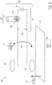
- Figure 1 is an example near-field antenna 100.
- the antenna 100 includes a coil (H-field) antenna 105 for magnetic fields, in conjunction with a short loaded dipole (E-field) antenna 120 for electric fields.
- the H-field antenna 105 includes a ferrite core 110 wound with wire 115.
- the E-field antenna 120 includes two conductive loading structures 125 and 130.
- Antenna 100 feed points 135, 140 are coupled to various tuning, measurement, and/or transceiver circuitry, such as downstream resonance frequency and bandwidth tuning banks, current sensors, and radio transmitter and receiver integrated circuit (RF-IC).
- RF-IC radio transmitter and receiver integrated circuit
- the magnetic and electric fields that are substantially confined to the structure and not significantly radiate in free-space can in some example embodiments be measured with much greater sensitivity.
- the antenna 100 operates at or below 50 MHz (e.g. for example at 30 MHz) to ensure that the fields are following the structure's contours and to ensure that far field radiation is strongly reduced.
- the near-field antenna 100 shown is an NFEMI antenna
- just the coil (H-field) antenna 105 or the short loaded dipole (E-field) antenna 120 could be separately used if only magnetic (H) fields or electric (E) fields are to be respectively sensed and measured.
- Figure 2 is an example of a first near-field measurement device 200.
- the first near-field measuring device 200 includes the near-field antenna 100, supporting circuits 202, and configured to receive non-propagating quasi-static near-field signals.
- the near-field measuring device 200 is configured to receive and measure a non-propagating quasi-static near-field signal.
- the near-field antenna 100 may in some example embodiments also be coupled to a transmitter circuit (not shown) for two-way communications.
- the example idealized antenna 100 includes the magnetic (H-field) antenna 105 having a resistance (R3) and an inductance (LI), the electric (E-field) antenna 120 having a conductive structure formed from the two loading plates 125 and 130 and a resistance (R4), and the two feeding points 135, 140.
- the supporting circuits 202 include a tuning circuit 204, a current sensor 206, and a controller 216.
- the tuning circuit 204 is coupled to the first and second feed points 135, 140.
- the tuning circuit 204 includes a first variable tuning capacitance bank (C1), a second variable tuning capacitance bank (C2), a first variable tuning resistance bank (R1), and a second variable tuning resistance bank (R2).
- the capacitance banks and resistance banks are coupled to a ground 224.
- the capacitive banks are coupled to the controller 216 by control line 218, and the resistance banks are coupled to the controller 216 by control line 220.
- the controller 216 adjusts the first and second capacitance banks (C1), (C2) to adjust a resonant frequency of the magnetic 105 and the electric 120 antennas (e.g. to 10.6 MHz).
- the controller 216 adjusts the first and second resistance banks (R1), (R2) to adjust a bandwidth of the magnetic 105 and the electric 120 antennas (e.g. to 400 KHz) sufficient to allow the non-propagating quasi-static near-field signal to be received from the antennas 105, 120.
- the capacitance banks (C1), (C2) are equally tuned using the control line 218 from the controller 216, and the resistance banks (R1), (R2) are equally tuned using the control line 220 from the controller 216.
- the current sensor 206 includes a primary winding 208 galvanically coupled to the near-field antenna 100 and the tuning circuit 204.
- the current sensor 206 also includes a secondary winding 210 inductively coupled to the primary winding 208 via an optional ferrite core 212 and to a sensing element 214 (e.g. resistor).
- the current sensor 206 in some example embodiments is a transformer or toroidal coil.
- the current sensor 206 inductively couples the near-field antenna 100 to the sensing element 214 to help reduce current draw, enable greater sensitivity, and minimize loading of the near-field antenna 100 for improved near-field sensitivity.
- the inductively sensed resonant current is converted to a voltage across the sensing element 214 for further instrument capture and analysis.
- the controller 216 is then coupled to receive a signal (e.g. voltage) from the sensing element 214 by a measure line 222.
- a signal e.g. voltage
- the signal generated across the sensing element 214 can be measured by the controller 216.
- the voltage generated can in some example embodiments be used as frontend for a baseband receiver in a body communication device.
- Figure 3 is an example application 300 of a second near-field measurement device 302.
- This second near-field measurement device 302 used in this example application 300 is a modified version of the first near-field measuring device 200.
- the coil (H-field) antenna 105, conductive surfaces 125, 130 and the current sensor 206 are the same as for the first near-field measuring device 200; however, the second near-field measurement device 302 includes different tuning circuit 304 that instead includes a fixed tuning capacitance 306 and a fixed tuning resistance 308.
- tuning capacitor 306 may be 60 pF and the tuning resistance 308 may be 12 kOhm.
- the second near-field measurement device 302 is positioned close to a conductive structure 310 (e.g. a human body).
- the conductive structure 310 forms a capacitance 312 (e.g. 100 pF) with the ground 224.
- Conductive surface 130 is positioned close to the conductive structure 310 and located at the position where the electric and/or the magnetic fields are to be measured.
- Conductive surface 125 is positioned further away from the conductive structure 310 compared with the conductive surface 130. Both conductive surfaces 125, 130 together form their own capacitance. The capacitance value is depending on the dimensions but practical values can be in the order of 5 pF.
- both conductive surfaces 125, 130 are in the presence of an electric (E-field) 316, a voltage is induced between them and since the conductive surface 130 is close to the conductive structure 310 the electric (E-field) 316 present on the conductive structure 310 will induce a voltage between both surfaces 125, 130.
- the near-field measuring device's 302 tuning capacitance 306 is much larger than the capacitance between the conductive surfaces 125, 130. In such embodiments, a large part of the second near-field measurement device's 302 resonance current flows through the tuning capacitance 306 and thus the primary winding 208 portion of the current sensor 206 is positioned between the tuning capacitance 306 and the tuning resistance 308 as shown in Figure 3 .
- the controller 212 is not shown in this figure but would be coupled to the sensing element 214 of the current sensor 206 as discussed in Figure 2 .
- Figure 4 is an example application 400 of a third near-field measurement device 402.
- the third near-field measurement device 402 is similar to the second near-field measurement device 302, however a different current sensor 404 is included.
- the current sensor 404 includes the primary winding 208, the secondary winding 210, and an optional ferrite core 212; however a new sensing element 406 is included.
- the sensing element 406 includes a first LNA 408, a filter 410, a second LNA 412, and an output 414.
- the first LNA 408 is connected to the secondary winding 210 and converts the secondary winding 210 current into an amplified voltage. This amplified voltage can be directly coupled to a measurement instrument or baseband communications circuit for further processing.
- the second LNA 412 may be used to provide sufficient output voltage so that the measurement instrument or baseband communications circuit has sufficient signal strength.
- the output 414 may be connected to the measurement instrument or baseband communications circuit with a coaxial cable.
- the measurement instrument or baseband communications circuit can be capacitively coupled to ground 224 via their mains power supply.
- Grounding 224 of the mains power supply enables more accurate sensing of the electric fields such that the measurement instrument or baseband communications circuit do not themselves become part of the antennas and thereby overestimate the measured currents.
- these near-field measurement devices 200, 302, 402 include: monitoring a quality of on-body links, use as a new frontend for applications with industrial interference, as a measuring device for Human Exposure to wireless body area devices, or for regular near-field (e.g. NFEMI, NFEI, NFMI, etc.) communications.
- regular near-field e.g. NFEMI, NFEI, NFMI, etc.
- a near-field measuring device including: a near-field antenna; a tuning circuit galvanically coupled to the near-field antenna and configured to set a resonant frequency and/or a quality factor of the measuring device; and a current sensor inductively coupled to the near-field antenna and configured to generate a signal in response to a current flowing through the galvanic coupling between the near-field antenna and the tuning circuit; wherein the signal represents a measurement of non-propagating quasi-static near-field signals received by the near-field antenna.
- these instructions/steps are implemented as functional and software instructions.
- the instructions can be implemented either using logic gates, application specific chips, firmware, as well as other hardware forms.
- the instructions are embodied as a set of executable instructions in a non-transitory computer-readable or computer-usable media which are effected on a computer or machine programmed with and controlled by said executable instructions.
- Said instructions are loaded for execution on a processor (such as one or more CPUs).
- Said processor includes microprocessors, microcontrollers, processor modules or subsystems (including one or more microprocessors or microcontrollers), or other control or computing devices.
- a processor can refer to a single component or to plural components.
- Said computer-readable or computer-usable storage medium or media is (are) considered to be part of an article (or article of manufacture).
- An article or article of manufacture can refer to any manufactured single component or multiple components.
- the non-transitory machine or computer-usable media or mediums as defined herein excludes signals, but such media or mediums may be capable of receiving and processing information from signals and/or other transitory mediums.
Description
- The present specification relates to systems, methods, apparatuses, devices, articles of manufacture and instructions for near-field measurement.
- According to an example embodiment, a near-field measuring device, comprising: a near-field antenna; a tuning circuit galvanically coupled to the near-field antenna and configured to set a resonant frequency and/or a quality factor of the measuring device; and a current sensor inductively coupled to the near-field antenna and configured to generate a signal in response to a current flowing through the galvanic coupling between the near-field antenna and the tuning circuit; wherein the signal represents a measurement of non-propagating quasi-static near-field signals received by the near-field antenna.
- In another example embodiment, the current sensor is a transformer or a toroidal coil.
- In another example embodiment, the current sensor is configured to amplify the current flowing in the galvanic coupling.
- In another example embodiment, the tuning circuit includes a capacitance and a resistance.
- In another example embodiment, the near-field antenna includes a set of conductive surfaces configured to be responsive to an electric near-field signal; the conductive surfaces together form a capacitance; the tuning circuit capacitance is larger than the conductive surfaces capacitance such that a larger portion of the current flowing through near-field antenna flows through the tuning circuit capacitance; and the current sensor is inductively coupled in series with the tuning circuit capacitance and coupled in parallel with the tuning circuit resistance.
- In another example embodiment, further comprising a sensing element; wherein the current sensor includes a primary winding and a secondary winding; wherein the primary winding is galvanically coupled to the near-field antenna; and wherein the secondary winding is inductively coupled to the primary winding, and galvanically coupled to the sensing element.
- In another example embodiment, the sensing element includes a resistance; the signal is a voltage; and the resistance is configured to generate the voltage in response to the current flowing through the primary winding.
- In another example embodiment, the sensing element includes a low noise amplifier; the signal is a voltage; and the low noise amplifier is configured to generate an amplified output signal in response to the current flowing through the primary winding.
- In another example embodiment, the sensing element is configured to be coupled to a measurement instrument; and the measurement instrument is configured to output either a magnetic near-field strength signal and/or an electric near-field strength signal in response to the current flowing through the primary winding.
- In another example embodiment, the sensing element is configured to be coupled to a baseband communications circuit; and the communications circuit is configured to output a communications signal in response to the current flowing through the primary winding.
- In another example embodiment, the tuning circuit includes a variable tuning capacitance bank configured to set a resonant frequency of the near-field antenna in response to a control line.
- In another example embodiment, the tuning circuit includes a variable tuning resistance bank configured to set a quality factor or bandwidth of the near-field antenna in response to a control line.
- In another example embodiment, the tuning circuit includes a fixed tuning capacitance configured to set a fixed resonant frequency of the near-field antenna and a fixed tuning resistance configured to set a fixed quality factor or bandwidth of the near-field antenna.
- In another example embodiment, the current flowing in the galvanic coupling between the near-field antenna and the tuning circuit is generated only by the non-propagating quasi-static near-field signals received by the near-field antenna.
- In another example embodiment, the near-field antenna is a near-field magnetic antenna responsive to non-propagating quasi-static near-field magnetic signals.
- In another example embodiment, the near-field antenna is a near-field electric antenna responsive to non-propagating quasi-static near-field electric signals.
- In another example embodiment, the near-field antenna is a near-field electromagnetic antenna responsive to non-propagating quasi-static near-field electric and magnetic signals.
- In another example embodiment, the near-field measuring device is configured to be capacitively coupled to an external conductive surface from which the measurement of non-propagating quasi-static near-field signals is to be made.
- In another example embodiment, the near-field measuring device is embedded in at least one of: a wearable device; a smart watch; a smartwatch housing, an earbud, a hearing aid, a medical device, an activity tracker, or a heart rate monitor.
- The above discussion is not intended to represent every example embodiment or every implementation within the scope of the current or future Claim sets. The Figures and Detailed Description that follow also exemplify various example embodiments.
- Various example embodiments may be more completely understood in consideration of the following Detailed Description in connection with the accompanying Drawings.
-
-
Figure 1 is an example near-field antenna. -
Figure 2 is an example of a first near-field measurement device. -
Figure 3 is an example application of a second near-field measurement device. -
Figure 4 is an example application of a third near-field measurement device. - While the disclosure is amenable to various modifications and alternative forms, specifics thereof have been shown by way of example in the drawings and will be described in detail. The scope of the invention is defined by the appended claims.
- Herein discussed are near-field interactions between a near-field device, perhaps on a user's body, and other conductive surfaces and/or other wireless networked devices (e.g. Internet of Things (IoT) devices, wearables, earbuds, body area networks, gaming products and medical products like continuous glucose monitoring, etc.) based on near-field electromagnetic induction (NFEMI), where the transmitter and receiver are coupled by both magnetic (H) and electric (E) fields. While RF wireless communication is accomplished by propagating an RF plane wave through free space, NFEMI communication utilizes non-propagating quasi-static H and E fields.
- An H-field antenna (i.e. magnetic antenna) is primarily sensitive to magnetic fields and/or primarily initiates magnetic fields when driven by a current. Any E-field component from an H-field antenna is strongly reduced (e.g. -20 to -60 dB reduction, a factor of 0.1 to 0.0008 (10% to 0.08%) depending on the antenna design).
- A small loop antenna is an example H-field antenna and includes a loop antenna with dimensions much smaller than the wavelength of its use. The small loop antenna does not resonate at the NFEMI carrier frequency but is instead tuned to resonance by an external reactance. In some example embodiments the current in the small loop antenna has in every position of the loop the same value.
- An E-field antenna (i.e. electric antenna) is primarily sensitive to electric fields and/or primarily initiates electric fields when driven by a voltage. Any H-field component from an E-field antenna is strongly reduced (e.g. -20 to -60 dB reduction, a factor of 0.1 to 0.0008 (10% to 0.08%) depending on the antenna design).
- A short loaded dipole antenna is an example E-field antenna and includes a short dipole with dimensions much smaller than the NFEMI carrier frequency and in some example embodiments has extra capacitance surfaces at both ends.
- The quasi-static characteristic of these fields is a result of the NFEMI antenna dimensions in combination with their carrier frequencies. Most of the near-field energy is stored in the form of magnetic and electric fields, while a small amount of RF energy inevitably propagates in free space. Small antenna geometries minimize radiating waves in free space.
- Some wearables, such as hearing aids and wireless earbuds, employ Near-Field Magnetic Induction (NFMI) as a wireless communication method. In NFMI wireless communication, two loosely coupled coils realize signal transfer. No radiation of radio waves takes place. A current flowing in the transmission coil generates a H-field which in turn induces a current in the receiving coil. In this way, wireless communication is accomplished. Unfortunately, H-field based NFMI systems with small antenna coils have a limited range that may be much smaller than an entire wearable user's body. Such H-field communications are sensitive to coil orientation. In the case of a hearing aid form factor, a H-field induction based system cannot cover an entire human body. However, since in hearing aids both coils are always aligned with each other, they are not influenced by the movement of the human body.
- Other wearables employ Near-field Electric Induction (NFEI)) as a wireless communication method. NFEI allows electronic devices on and near a conductive surface (e.g. a human body) to exchange information through E-field coupling (e.g. at 21 MHz). NFEI is also sometimes called Body Coupled Communication (BCC). While E-field based NFEI signals can have a greater range than H-field based NFMI signals, the E-field signal strength can vary with regard to body posture and is sensitive to body movements. The body can even partially block a capacitive return path, thereby increasing E-field channel loss and reliable and robust wireless communication is not possible.
- Ensuring robust near-field communications however may require carefully measuring and characterizing the near-field environment (e.g. normal body generated fields, noise, other devices, etc.) surrounding such devices. Such near-field signals can be very difficult to measure since they are concentrated very close to a user's body and have relatively low amplitudes.
- Existing electric and magnetic field measuring instruments are designed for measuring much stronger and further distant far-field signals (e.g. for electromagnetic compatibility (EMC) and radiation patterns, etc.). Such instruments may only be capable of electromagnetic field strengths as low as 500mV/m. Examples of near-field devices existing in prior art can be seen in
US 10 277 284 B1 US 10 491 270 B1 - Now discussed are example embodiments of a near-field measuring device tailored to measuring these concentrated, low level near-field signals near conductive body surfaces and/or in surrounding environments. These example embodiments are capable of measuring electromagnetic field strengths as low as 10mV/m. Once captured, these near-field signals can then be recorded and characterized by additional diagnostic devices such as a frequency spectrum analyzers or oscilloscopes.
-
Figure 1 is an example near-field antenna 100. In some example embodiments, theantenna 100 includes a coil (H-field)antenna 105 for magnetic fields, in conjunction with a short loaded dipole (E-field)antenna 120 for electric fields. The H-field antenna 105 includes aferrite core 110 wound withwire 115. TheE-field antenna 120 includes twoconductive loading structures Antenna 100feed points - When the
NFEMI antenna 100 is proximate to a structure (e.g. a conductive structure, a body, a person, an object, etc.) the magnetic and electric fields that are substantially confined to the structure and not significantly radiate in free-space can in some example embodiments be measured with much greater sensitivity. - In various example embodiments, the
antenna 100 operates at or below 50 MHz (e.g. for example at 30 MHz) to ensure that the fields are following the structure's contours and to ensure that far field radiation is strongly reduced. - While the near-
field antenna 100 shown is an NFEMI antenna, in other example embodiments just the coil (H-field)antenna 105 or the short loaded dipole (E-field)antenna 120 could be separately used if only magnetic (H) fields or electric (E) fields are to be respectively sensed and measured. -
Figure 2 is an example of a first near-field measurement device 200. The first near-field measuring device 200 includes the near-field antenna 100, supportingcircuits 202, and configured to receive non-propagating quasi-static near-field signals. The near-field measuring device 200 is configured to receive and measure a non-propagating quasi-static near-field signal. Note that the near-field antenna 100 may in some example embodiments also be coupled to a transmitter circuit (not shown) for two-way communications. - The example idealized
antenna 100 includes the magnetic (H-field)antenna 105 having a resistance (R3) and an inductance (LI), the electric (E-field)antenna 120 having a conductive structure formed from the twoloading plates feeding points - The supporting
circuits 202 include atuning circuit 204, acurrent sensor 206, and acontroller 216. - The
tuning circuit 204 is coupled to the first and second feed points 135, 140. Thetuning circuit 204 includes a first variable tuning capacitance bank (C1), a second variable tuning capacitance bank (C2), a first variable tuning resistance bank (R1), and a second variable tuning resistance bank (R2). The capacitance banks and resistance banks are coupled to aground 224. The capacitive banks are coupled to thecontroller 216 bycontrol line 218, and the resistance banks are coupled to thecontroller 216 bycontrol line 220. - The
controller 216 adjusts the first and second capacitance banks (C1), (C2) to adjust a resonant frequency of the magnetic 105 and the electric 120 antennas (e.g. to 10.6 MHz). Thecontroller 216 adjusts the first and second resistance banks (R1), (R2) to adjust a bandwidth of the magnetic 105 and the electric 120 antennas (e.g. to 400 KHz) sufficient to allow the non-propagating quasi-static near-field signal to be received from theantennas - The capacitance banks (C1), (C2) are equally tuned using the
control line 218 from thecontroller 216, and the resistance banks (R1), (R2) are equally tuned using thecontrol line 220 from thecontroller 216. - The
current sensor 206 includes a primary winding 208 galvanically coupled to the near-field antenna 100 and thetuning circuit 204. Thecurrent sensor 206 also includes a secondary winding 210 inductively coupled to the primary winding 208 via anoptional ferrite core 212 and to a sensing element 214 (e.g. resistor). Thecurrent sensor 206 in some example embodiments is a transformer or toroidal coil. - The
current sensor 206 inductively couples the near-field antenna 100 to thesensing element 214 to help reduce current draw, enable greater sensitivity, and minimize loading of the near-field antenna 100 for improved near-field sensitivity. The inductively sensed resonant current is converted to a voltage across thesensing element 214 for further instrument capture and analysis. - The
controller 216 is then coupled to receive a signal (e.g. voltage) from thesensing element 214 by ameasure line 222. - When the near-
field measuring device 200 is receiving the non-propagating quasi-static near-field signal, the signal generated across thesensing element 214 can be measured by thecontroller 216. The voltage generated can in some example embodiments be used as frontend for a baseband receiver in a body communication device. -
Figure 3 is anexample application 300 of a second near-field measurement device 302. This second near-field measurement device 302 used in thisexample application 300 is a modified version of the first near-field measuring device 200. - The coil (H-field)
antenna 105,conductive surfaces current sensor 206 are the same as for the first near-field measuring device 200; however, the second near-field measurement device 302 includesdifferent tuning circuit 304 that instead includes a fixedtuning capacitance 306 and a fixedtuning resistance 308. - These fixed tuning parameters result in a more
compact device 302 that is tuned to a particular resonance frequency and bandwidth for a particular set of applications. For example if a measurement is required at 10 MHz with a bandwidth of 400 kHz, thetuning capacitor 306 may be 60 pF and the tuningresistance 308 may be 12 kOhm. - The second near-
field measurement device 302 is positioned close to a conductive structure 310 (e.g. a human body). Theconductive structure 310 forms a capacitance 312 (e.g. 100 pF) with theground 224. -
Conductive surface 130 is positioned close to theconductive structure 310 and located at the position where the electric and/or the magnetic fields are to be measured.Conductive surface 125, is positioned further away from theconductive structure 310 compared with theconductive surface 130. Bothconductive surfaces - When both
conductive surfaces conductive surface 130 is close to theconductive structure 310 the electric (E-field) 316 present on theconductive structure 310 will induce a voltage between bothsurfaces conductive structure 310 in case it is a living body, will also induce a voltage in themagnetic coil antenna 105. - In some example embodiments, the near-field measuring device's 302
tuning capacitance 306 is much larger than the capacitance between theconductive surfaces tuning capacitance 306 and thus the primary winding 208 portion of thecurrent sensor 206 is positioned between the tuningcapacitance 306 and the tuningresistance 308 as shown inFigure 3 . - The
controller 212 is not shown in this figure but would be coupled to thesensing element 214 of thecurrent sensor 206 as discussed inFigure 2 . -
Figure 4 is anexample application 400 of a third near-field measurement device 402. The third near-field measurement device 402 is similar to the second near-field measurement device 302, however a differentcurrent sensor 404 is included. Thecurrent sensor 404 includes the primary winding 208, the secondary winding 210, and anoptional ferrite core 212; however anew sensing element 406 is included. - The
sensing element 406 includes afirst LNA 408, afilter 410, asecond LNA 412, and anoutput 414. Thefirst LNA 408 is connected to the secondary winding 210 and converts the secondary winding 210 current into an amplified voltage. This amplified voltage can be directly coupled to a measurement instrument or baseband communications circuit for further processing. - However, if the
filter 410 is included thesecond LNA 412 may be used to provide sufficient output voltage so that the measurement instrument or baseband communications circuit has sufficient signal strength. - Also the
output 414 may be connected to the measurement instrument or baseband communications circuit with a coaxial cable. The measurement instrument or baseband communications circuit can be capacitively coupled toground 224 via their mains power supply. - Grounding 224 of the mains power supply enables more accurate sensing of the electric fields such that the measurement instrument or baseband communications circuit do not themselves become part of the antennas and thereby overestimate the measured currents.
- Thus capacitive currents on the cables and conductive parts of the
LNAs current sensor 404 in a series configuration with thetuning capacitor 306 and by reducing any stray capacitance between the primary and secondary windings of the current sensor and alldevice 402 elements are coupled toground 224. - Various applications of these near-
field measurement devices - One example discloses a near-field measuring device, including: a near-field antenna; a tuning circuit galvanically coupled to the near-field antenna and configured to set a resonant frequency and/or a quality factor of the measuring device; and a current sensor inductively coupled to the near-field antenna and configured to generate a signal in response to a current flowing through the galvanic coupling between the near-field antenna and the tuning circuit; wherein the signal represents a measurement of non-propagating quasi-static near-field signals received by the near-field antenna.
- Various instructions and/or operational steps discussed in the above Figures can be executed in any order, unless a specific order is explicitly stated. Also, those skilled in the art will recognize that while some example sets of instructions/steps have been discussed, the material in this specification can be combined in a variety of ways to yield other examples as well, and are to be understood within a context provided by this detailed description.
- In some example embodiments these instructions/steps are implemented as functional and software instructions. In other embodiments, the instructions can be implemented either using logic gates, application specific chips, firmware, as well as other hardware forms.
- When the instructions are embodied as a set of executable instructions in a non-transitory computer-readable or computer-usable media which are effected on a computer or machine programmed with and controlled by said executable instructions. Said instructions are loaded for execution on a processor (such as one or more CPUs). Said processor includes microprocessors, microcontrollers, processor modules or subsystems (including one or more microprocessors or microcontrollers), or other control or computing devices. A processor can refer to a single component or to plural components. Said computer-readable or computer-usable storage medium or media is (are) considered to be part of an article (or article of manufacture). An article or article of manufacture can refer to any manufactured single component or multiple components. The non-transitory machine or computer-usable media or mediums as defined herein excludes signals, but such media or mediums may be capable of receiving and processing information from signals and/or other transitory mediums.
- It will be readily understood that the components of the embodiments as generally described herein and illustrated in the appended figures could be arranged and designed in a wide variety of different configurations. Thus, the detailed description of various embodiments, as represented in the figures, is not intended to limit the scope of the present disclosure, but is merely representative of various embodiments. While the various aspects of the embodiments are presented in drawings, the drawings are not necessarily drawn to scale unless specifically indicated.
- The invention is defined by the appended claims.
- Reference throughout this specification to features, advantages, or similar language does not imply that all of the features and advantages that may be realized with the present invention should be or are in any single embodiment of the invention. Rather, language referring to the features and advantages is understood to mean that a specific feature, advantage, or characteristic described in connection with an embodiment is included in at least one embodiment of the present invention. Thus, discussions of the features and advantages, and similar language, throughout this specification may, but do not necessarily, refer to the same embodiment.
- Furthermore, the described features, advantages, and characteristics of the invention may be combined in any suitable manner in one or more embodiments. One skilled in the relevant art will recognize, in light of the description herein, that the invention can be practiced without one or more of the specific features or advantages of a particular embodiment. In other instances, additional features and advantages may be recognized in certain embodiments that may not be present in all embodiments of the invention.
- Reference throughout this specification to "one embodiment," "an embodiment," or similar language means that a particular feature, structure, or characteristic described in connection with the indicated embodiment is included in at least one embodiment of the present invention. Thus, the phrases "in one embodiment," "in an embodiment," and similar language throughout this specification may, but do not necessarily, all refer to the same embodiment.
Claims (15)
- A near-field measuring device, comprising:a near-field antenna (100);a tuning circuit (204) galvanically coupled to the near-field antenna and configured to set a resonant frequency and/or a quality factor of the measuring device; characterized bya current sensor (206) inductively coupled to the near-field antenna and configured to generate a signal in response to a current flowing through the galvanic coupling between the near-field antenna and the tuning circuit;wherein the signal represents a measurement of non-propagating quasi-static near-field signals received by the near-field antenna.
- The device of claim 1:
wherein the current sensor is a transformer or a toroidal coil. - The device of claim 1 or 2:
wherein the current sensor is configured to amplify the current flowing in the galvanic coupling. - The device of any preceding claim:
wherein the tuning circuit includes a capacitance and a resistance. - The device of claim 4:wherein the near-field antenna includes a set of conductive surfaces configured to be responsive to an electric near-field signal;wherein the conductive surfaces together form a capacitance;wherein the tuning circuit capacitance is larger than the conductive surfaces capacitance such that a larger portion of the current flowing through near-field antenna flows through the tuning circuit capacitance; andwherein the current sensor is inductively coupled in series with the tuning circuit capacitance and coupled in parallel with the tuning circuit resistance.
- The device of any preceding claim:further comprising a sensing element;wherein the current sensor includes a primary winding and a secondary winding;wherein the primary winding is galvanically coupled to the near-field antenna; andwherein the secondary winding is inductively coupled to the primary winding, and galvanically coupled to the sensing element.
- The device of claim 6:wherein the sensing element includes a resistance;wherein the signal is a voltage; andwherein the resistance is configured to generate the voltage in response to the current flowing through the primary winding.
- The device of claim 6 or 7:wherein the sensing element includes a low noise amplifier;wherein the signal is a voltage; andwherein the low noise amplifier is configured to generate an amplified output signal in response to the current flowing through the primary winding.
- The device of any of claims 6 to 8:wherein the sensing element is configured to be coupled to a measurement instrument; andwherein the measurement instrument is configured to output either a magnetic near-field strength signal and/or an electric near-field strength signal in response to the current flowing through the primary winding.
- The device of any of claims 6 to 9:wherein the sensing element is configured to be coupled to a baseband communications circuit; andwherein the communications circuit is configured to output a communications signal in response to the current flowing through the primary winding.
- The device of any preceding claim:
wherein the tuning circuit includes a variable tuning capacitance bank configured to set a resonant frequency of the near-field antenna in response to a control line. - The device of any preceding claim:
wherein the tuning circuit includes a variable tuning resistance bank configured to set a quality factor or bandwidth of the near-field antenna in response to a control line. - The device of any preceding claim:
wherein the tuning circuit includes a fixed tuning capacitance configured to set a fixed resonant frequency of the near-field antenna and a fixed tuning resistance configured to set a fixed quality factor or bandwidth of the near-field antenna. - The device of any preceding claim:
wherein the current flowing in the galvanic coupling between the near-field antenna and the tuning circuit is generated only by the non-propagating quasi-static near-field signals received by the near-field antenna. - The device of any preceding claim:
wherein the near-field antenna is a near-field magnetic antenna responsive to non-propagating quasi-static near-field magnetic signals.
Applications Claiming Priority (1)
| Application Number | Priority Date | Filing Date | Title |
|---|---|---|---|
| US16/840,495 US10826627B1 (en) | 2020-04-06 | 2020-04-06 | Near-field measuring device |
Publications (2)
| Publication Number | Publication Date |
|---|---|
| EP3896863A1 EP3896863A1 (en) | 2021-10-20 |
| EP3896863B1 true EP3896863B1 (en) | 2022-12-28 |
Family
ID=73019787
Family Applications (1)
| Application Number | Title | Priority Date | Filing Date |
|---|---|---|---|
| EP21165364.7A Active EP3896863B1 (en) | 2020-04-06 | 2021-03-26 | Near-field measuring device |
Country Status (3)
| Country | Link |
|---|---|
| US (1) | US10826627B1 (en) |
| EP (1) | EP3896863B1 (en) |
| CN (1) | CN113498048A (en) |
Families Citing this family (1)
| Publication number | Priority date | Publication date | Assignee | Title |
|---|---|---|---|---|
| US11677151B2 (en) * | 2020-09-11 | 2023-06-13 | Nxp B.V. | Near-field communications device |
Family Cites Families (8)
| Publication number | Priority date | Publication date | Assignee | Title |
|---|---|---|---|---|
| US20070218837A1 (en) * | 2006-03-14 | 2007-09-20 | Sony Ericsson Mobile Communications Ab | Data communication in an electronic device |
| WO2009066211A2 (en) * | 2007-11-19 | 2009-05-28 | Nxp B.V. | Transceiving circuit for contactless communication |
| US8274386B1 (en) | 2009-03-23 | 2012-09-25 | The United States Of America As Represented By The Secretary Of The Navy | Human presence electric field sensor |
| FR2945137B1 (en) * | 2009-04-30 | 2011-06-24 | Pascal Metivier | PROGRAMMING SYSTEM FOR A LOCK COMPRISING NFC-CONTACTLESS CONTACT COMMUNICATION MEANS |
| KR102496942B1 (en) * | 2015-08-24 | 2023-02-06 | 더 리젠츠 오브 더 유니버시티 오브 캘리포니아 | Low Power Magnetic Field Body Area Networks |
| US10978791B2 (en) * | 2018-05-07 | 2021-04-13 | Nxp B.V. | Combination antenna |
| US10277284B1 (en) * | 2018-11-20 | 2019-04-30 | Nxp B.V. | Near-field device |
| US10491270B1 (en) * | 2018-11-26 | 2019-11-26 | Nxp B.V. | Near-field device |
-
2020
- 2020-04-06 US US16/840,495 patent/US10826627B1/en active Active
-
2021
- 2021-03-26 EP EP21165364.7A patent/EP3896863B1/en active Active
- 2021-04-06 CN CN202110369902.2A patent/CN113498048A/en active Pending
Also Published As
| Publication number | Publication date |
|---|---|
| CN113498048A (en) | 2021-10-12 |
| US10826627B1 (en) | 2020-11-03 |
| EP3896863A1 (en) | 2021-10-20 |
Similar Documents
| Publication | Publication Date | Title |
|---|---|---|
| CN108461901B (en) | Near field electromagnetic induction (NFEMI) antenna | |
| US11011826B2 (en) | Near-field electromagnetic induction (NFEMI) device | |
| EP3389135B1 (en) | Near-field electromagnetic induction (nfemi) antenna | |
| EP3930206A1 (en) | Near-field communications device | |
| US10862542B1 (en) | Near-field converter | |
| EP3687077A1 (en) | Near-field communications device | |
| EP3910803B1 (en) | Near-field wireless device | |
| EP3787192B1 (en) | Quality-factor control for a near-field wireless device | |
| US10763921B1 (en) | Near-field electromagnetic induction device | |
| EP3691135A1 (en) | Near-field communications device | |
| EP3934116A1 (en) | Near-field communications device | |
| EP3917022B1 (en) | Near-field wireless device | |
| EP3863186A1 (en) | Near-field electromagnetic induction (nfemi) antenna | |
| EP3896863B1 (en) | Near-field measuring device | |
| US10812126B1 (en) | Near-field device including multiple conductive plates | |
| EP3553959B1 (en) | Wireless device | |
| EP3866345B1 (en) | Near-field electromagnetic induction (nfemi) antenna | |
| EP3972143A1 (en) | Near-field communication device with variable path-loss |
Legal Events
| Date | Code | Title | Description |
|---|---|---|---|
| PUAI | Public reference made under article 153(3) epc to a published international application that has entered the european phase |
Free format text: ORIGINAL CODE: 0009012 |
|
| STAA | Information on the status of an ep patent application or granted ep patent |
Free format text: STATUS: THE APPLICATION HAS BEEN PUBLISHED |
|
| AK | Designated contracting states |
Kind code of ref document: A1 Designated state(s): AL AT BE BG CH CY CZ DE DK EE ES FI FR GB GR HR HU IE IS IT LI LT LU LV MC MK MT NL NO PL PT RO RS SE SI SK SM TR |
|
| B565 | Issuance of search results under rule 164(2) epc |
Effective date: 20210922 |
|
| STAA | Information on the status of an ep patent application or granted ep patent |
Free format text: STATUS: REQUEST FOR EXAMINATION WAS MADE |
|
| 17P | Request for examination filed |
Effective date: 20220420 |
|
| RBV | Designated contracting states (corrected) |
Designated state(s): AL AT BE BG CH CY CZ DE DK EE ES FI FR GB GR HR HU IE IS IT LI LT LU LV MC MK MT NL NO PL PT RO RS SE SI SK SM TR |
|
| RIC1 | Information provided on ipc code assigned before grant |
Ipc: G01R 29/08 20060101ALI20220722BHEP Ipc: H04B 5/00 20060101AFI20220722BHEP |
|
| GRAP | Despatch of communication of intention to grant a patent |
Free format text: ORIGINAL CODE: EPIDOSNIGR1 |
|
| STAA | Information on the status of an ep patent application or granted ep patent |
Free format text: STATUS: GRANT OF PATENT IS INTENDED |
|
| INTG | Intention to grant announced |
Effective date: 20220920 |
|
| GRAS | Grant fee paid |
Free format text: ORIGINAL CODE: EPIDOSNIGR3 |
|
| GRAA | (expected) grant |
Free format text: ORIGINAL CODE: 0009210 |
|
| STAA | Information on the status of an ep patent application or granted ep patent |
Free format text: STATUS: THE PATENT HAS BEEN GRANTED |
|
| AK | Designated contracting states |
Kind code of ref document: B1 Designated state(s): AL AT BE BG CH CY CZ DE DK EE ES FI FR GB GR HR HU IE IS IT LI LT LU LV MC MK MT NL NO PL PT RO RS SE SI SK SM TR |
|
| REG | Reference to a national code |
Ref country code: GB Ref legal event code: FG4D |
|
| REG | Reference to a national code |
Ref country code: CH Ref legal event code: EP |
|
| REG | Reference to a national code |
Ref country code: DE Ref legal event code: R096 Ref document number: 602021001072 Country of ref document: DE |
|
| REG | Reference to a national code |
Ref country code: AT Ref legal event code: REF Ref document number: 1541117 Country of ref document: AT Kind code of ref document: T Effective date: 20230115 |
|
| REG | Reference to a national code |
Ref country code: IE Ref legal event code: FG4D |
|
| REG | Reference to a national code |
Ref country code: LT Ref legal event code: MG9D |
|
| PG25 | Lapsed in a contracting state [announced via postgrant information from national office to epo] |
Ref country code: SE Free format text: LAPSE BECAUSE OF FAILURE TO SUBMIT A TRANSLATION OF THE DESCRIPTION OR TO PAY THE FEE WITHIN THE PRESCRIBED TIME-LIMIT Effective date: 20221228 Ref country code: NO Free format text: LAPSE BECAUSE OF FAILURE TO SUBMIT A TRANSLATION OF THE DESCRIPTION OR TO PAY THE FEE WITHIN THE PRESCRIBED TIME-LIMIT Effective date: 20230328 Ref country code: LT Free format text: LAPSE BECAUSE OF FAILURE TO SUBMIT A TRANSLATION OF THE DESCRIPTION OR TO PAY THE FEE WITHIN THE PRESCRIBED TIME-LIMIT Effective date: 20221228 Ref country code: FI Free format text: LAPSE BECAUSE OF FAILURE TO SUBMIT A TRANSLATION OF THE DESCRIPTION OR TO PAY THE FEE WITHIN THE PRESCRIBED TIME-LIMIT Effective date: 20221228 |
|
| PGFP | Annual fee paid to national office [announced via postgrant information from national office to epo] |
Ref country code: FR Payment date: 20230222 Year of fee payment: 3 |
|
| REG | Reference to a national code |
Ref country code: NL Ref legal event code: MP Effective date: 20221228 |
|
| REG | Reference to a national code |
Ref country code: AT Ref legal event code: MK05 Ref document number: 1541117 Country of ref document: AT Kind code of ref document: T Effective date: 20221228 |
|
| PG25 | Lapsed in a contracting state [announced via postgrant information from national office to epo] |
Ref country code: RS Free format text: LAPSE BECAUSE OF FAILURE TO SUBMIT A TRANSLATION OF THE DESCRIPTION OR TO PAY THE FEE WITHIN THE PRESCRIBED TIME-LIMIT Effective date: 20221228 Ref country code: LV Free format text: LAPSE BECAUSE OF FAILURE TO SUBMIT A TRANSLATION OF THE DESCRIPTION OR TO PAY THE FEE WITHIN THE PRESCRIBED TIME-LIMIT Effective date: 20221228 Ref country code: HR Free format text: LAPSE BECAUSE OF FAILURE TO SUBMIT A TRANSLATION OF THE DESCRIPTION OR TO PAY THE FEE WITHIN THE PRESCRIBED TIME-LIMIT Effective date: 20221228 Ref country code: GR Free format text: LAPSE BECAUSE OF FAILURE TO SUBMIT A TRANSLATION OF THE DESCRIPTION OR TO PAY THE FEE WITHIN THE PRESCRIBED TIME-LIMIT Effective date: 20230329 |
|
| PG25 | Lapsed in a contracting state [announced via postgrant information from national office to epo] |
Ref country code: NL Free format text: LAPSE BECAUSE OF FAILURE TO SUBMIT A TRANSLATION OF THE DESCRIPTION OR TO PAY THE FEE WITHIN THE PRESCRIBED TIME-LIMIT Effective date: 20221228 |
|
| PG25 | Lapsed in a contracting state [announced via postgrant information from national office to epo] |
Ref country code: SM Free format text: LAPSE BECAUSE OF FAILURE TO SUBMIT A TRANSLATION OF THE DESCRIPTION OR TO PAY THE FEE WITHIN THE PRESCRIBED TIME-LIMIT Effective date: 20221228 Ref country code: RO Free format text: LAPSE BECAUSE OF FAILURE TO SUBMIT A TRANSLATION OF THE DESCRIPTION OR TO PAY THE FEE WITHIN THE PRESCRIBED TIME-LIMIT Effective date: 20221228 Ref country code: PT Free format text: LAPSE BECAUSE OF FAILURE TO SUBMIT A TRANSLATION OF THE DESCRIPTION OR TO PAY THE FEE WITHIN THE PRESCRIBED TIME-LIMIT Effective date: 20230428 Ref country code: ES Free format text: LAPSE BECAUSE OF FAILURE TO SUBMIT A TRANSLATION OF THE DESCRIPTION OR TO PAY THE FEE WITHIN THE PRESCRIBED TIME-LIMIT Effective date: 20221228 Ref country code: EE Free format text: LAPSE BECAUSE OF FAILURE TO SUBMIT A TRANSLATION OF THE DESCRIPTION OR TO PAY THE FEE WITHIN THE PRESCRIBED TIME-LIMIT Effective date: 20221228 Ref country code: CZ Free format text: LAPSE BECAUSE OF FAILURE TO SUBMIT A TRANSLATION OF THE DESCRIPTION OR TO PAY THE FEE WITHIN THE PRESCRIBED TIME-LIMIT Effective date: 20221228 Ref country code: AT Free format text: LAPSE BECAUSE OF FAILURE TO SUBMIT A TRANSLATION OF THE DESCRIPTION OR TO PAY THE FEE WITHIN THE PRESCRIBED TIME-LIMIT Effective date: 20221228 |
|
| P01 | Opt-out of the competence of the unified patent court (upc) registered |
Effective date: 20230725 |
|
| PG25 | Lapsed in a contracting state [announced via postgrant information from national office to epo] |
Ref country code: SK Free format text: LAPSE BECAUSE OF FAILURE TO SUBMIT A TRANSLATION OF THE DESCRIPTION OR TO PAY THE FEE WITHIN THE PRESCRIBED TIME-LIMIT Effective date: 20221228 Ref country code: PL Free format text: LAPSE BECAUSE OF FAILURE TO SUBMIT A TRANSLATION OF THE DESCRIPTION OR TO PAY THE FEE WITHIN THE PRESCRIBED TIME-LIMIT Effective date: 20221228 Ref country code: IS Free format text: LAPSE BECAUSE OF FAILURE TO SUBMIT A TRANSLATION OF THE DESCRIPTION OR TO PAY THE FEE WITHIN THE PRESCRIBED TIME-LIMIT Effective date: 20230428 Ref country code: AL Free format text: LAPSE BECAUSE OF FAILURE TO SUBMIT A TRANSLATION OF THE DESCRIPTION OR TO PAY THE FEE WITHIN THE PRESCRIBED TIME-LIMIT Effective date: 20221228 |
|
| REG | Reference to a national code |
Ref country code: DE Ref legal event code: R097 Ref document number: 602021001072 Country of ref document: DE |
|
| PG25 | Lapsed in a contracting state [announced via postgrant information from national office to epo] |
Ref country code: MC Free format text: LAPSE BECAUSE OF FAILURE TO SUBMIT A TRANSLATION OF THE DESCRIPTION OR TO PAY THE FEE WITHIN THE PRESCRIBED TIME-LIMIT Effective date: 20221228 Ref country code: DK Free format text: LAPSE BECAUSE OF FAILURE TO SUBMIT A TRANSLATION OF THE DESCRIPTION OR TO PAY THE FEE WITHIN THE PRESCRIBED TIME-LIMIT Effective date: 20221228 |
|
| PLBE | No opposition filed within time limit |
Free format text: ORIGINAL CODE: 0009261 |
|
| STAA | Information on the status of an ep patent application or granted ep patent |
Free format text: STATUS: NO OPPOSITION FILED WITHIN TIME LIMIT |
|
| REG | Reference to a national code |
Ref country code: BE Ref legal event code: MM Effective date: 20230331 |
|
| 26N | No opposition filed |
Effective date: 20230929 |
|
| PG25 | Lapsed in a contracting state [announced via postgrant information from national office to epo] |
Ref country code: LU Free format text: LAPSE BECAUSE OF NON-PAYMENT OF DUE FEES Effective date: 20230326 |
|
| REG | Reference to a national code |
Ref country code: IE Ref legal event code: MM4A |
|
| PG25 | Lapsed in a contracting state [announced via postgrant information from national office to epo] |
Ref country code: SI Free format text: LAPSE BECAUSE OF FAILURE TO SUBMIT A TRANSLATION OF THE DESCRIPTION OR TO PAY THE FEE WITHIN THE PRESCRIBED TIME-LIMIT Effective date: 20221228 Ref country code: IE Free format text: LAPSE BECAUSE OF NON-PAYMENT OF DUE FEES Effective date: 20230326 |
|
| PG25 | Lapsed in a contracting state [announced via postgrant information from national office to epo] |
Ref country code: BE Free format text: LAPSE BECAUSE OF NON-PAYMENT OF DUE FEES Effective date: 20230331 |
|
| PGFP | Annual fee paid to national office [announced via postgrant information from national office to epo] |
Ref country code: DE Payment date: 20240220 Year of fee payment: 4 |