EP3851995A1 - Method for generating a unique data specific to an integrated silicon circuit - Google Patents
Method for generating a unique data specific to an integrated silicon circuit Download PDFInfo
- Publication number
- EP3851995A1 EP3851995A1 EP21151895.6A EP21151895A EP3851995A1 EP 3851995 A1 EP3851995 A1 EP 3851995A1 EP 21151895 A EP21151895 A EP 21151895A EP 3851995 A1 EP3851995 A1 EP 3851995A1
- Authority
- EP
- European Patent Office
- Prior art keywords
- signal
- event
- circuit
- tdc
- generator
- Prior art date
- Legal status (The legal status is an assumption and is not a legal conclusion. Google has not performed a legal analysis and makes no representation as to the accuracy of the status listed.)
- Granted
Links
- 238000000034 method Methods 0.000 title claims abstract description 37
- XUIMIQQOPSSXEZ-UHFFFAOYSA-N Silicon Chemical compound [Si] XUIMIQQOPSSXEZ-UHFFFAOYSA-N 0.000 title claims abstract description 8
- 229910052710 silicon Inorganic materials 0.000 title claims abstract description 8
- 239000010703 silicon Substances 0.000 title claims abstract description 8
- 238000005259 measurement Methods 0.000 claims description 50
- 230000001131 transforming effect Effects 0.000 claims description 8
- 238000007620 mathematical function Methods 0.000 claims description 3
- 230000000630 rising effect Effects 0.000 description 44
- 238000010586 diagram Methods 0.000 description 22
- 230000001934 delay Effects 0.000 description 21
- 230000004044 response Effects 0.000 description 19
- 238000004519 manufacturing process Methods 0.000 description 18
- 230000004913 activation Effects 0.000 description 13
- 230000006870 function Effects 0.000 description 12
- 235000021183 entrée Nutrition 0.000 description 5
- 238000012550 audit Methods 0.000 description 3
- 230000003111 delayed effect Effects 0.000 description 3
- 230000010355 oscillation Effects 0.000 description 3
- 230000008569 process Effects 0.000 description 3
- 230000002441 reversible effect Effects 0.000 description 3
- 238000007493 shaping process Methods 0.000 description 3
- 230000009466 transformation Effects 0.000 description 3
- 240000008042 Zea mays Species 0.000 description 2
- 238000004458 analytical method Methods 0.000 description 2
- 238000012937 correction Methods 0.000 description 2
- 230000008878 coupling Effects 0.000 description 2
- 230000005670 electromagnetic radiation Effects 0.000 description 2
- 238000005265 energy consumption Methods 0.000 description 2
- 238000011066 ex-situ storage Methods 0.000 description 2
- 238000011065 in-situ storage Methods 0.000 description 2
- 239000002184 metal Substances 0.000 description 2
- 239000002086 nanomaterial Substances 0.000 description 2
- 230000000087 stabilizing effect Effects 0.000 description 2
- 238000003860 storage Methods 0.000 description 2
- 230000006399 behavior Effects 0.000 description 1
- 238000004364 calculation method Methods 0.000 description 1
- 239000003990 capacitor Substances 0.000 description 1
- 230000001419 dependent effect Effects 0.000 description 1
- 238000005516 engineering process Methods 0.000 description 1
- 230000001747 exhibiting effect Effects 0.000 description 1
- 238000000605 extraction Methods 0.000 description 1
- 238000001914 filtration Methods 0.000 description 1
- 238000012544 monitoring process Methods 0.000 description 1
- 230000005693 optoelectronics Effects 0.000 description 1
- 230000003071 parasitic effect Effects 0.000 description 1
- 238000012805 post-processing Methods 0.000 description 1
- 230000000644 propagated effect Effects 0.000 description 1
- 230000001902 propagating effect Effects 0.000 description 1
- 230000003068 static effect Effects 0.000 description 1
- 238000011144 upstream manufacturing Methods 0.000 description 1
Images


Classifications
-
- H—ELECTRICITY
- H04—ELECTRIC COMMUNICATION TECHNIQUE
- H04L—TRANSMISSION OF DIGITAL INFORMATION, e.g. TELEGRAPHIC COMMUNICATION
- H04L9/00—Cryptographic mechanisms or cryptographic arrangements for secret or secure communications; Network security protocols
- H04L9/32—Cryptographic mechanisms or cryptographic arrangements for secret or secure communications; Network security protocols including means for verifying the identity or authority of a user of the system or for message authentication, e.g. authorization, entity authentication, data integrity or data verification, non-repudiation, key authentication or verification of credentials
- H04L9/3271—Cryptographic mechanisms or cryptographic arrangements for secret or secure communications; Network security protocols including means for verifying the identity or authority of a user of the system or for message authentication, e.g. authorization, entity authentication, data integrity or data verification, non-repudiation, key authentication or verification of credentials using challenge-response
- H04L9/3278—Cryptographic mechanisms or cryptographic arrangements for secret or secure communications; Network security protocols including means for verifying the identity or authority of a user of the system or for message authentication, e.g. authorization, entity authentication, data integrity or data verification, non-repudiation, key authentication or verification of credentials using challenge-response using physically unclonable functions [PUF]
-
- G—PHYSICS
- G06—COMPUTING; CALCULATING OR COUNTING
- G06F—ELECTRIC DIGITAL DATA PROCESSING
- G06F21/00—Security arrangements for protecting computers, components thereof, programs or data against unauthorised activity
- G06F21/70—Protecting specific internal or peripheral components, in which the protection of a component leads to protection of the entire computer
- G06F21/71—Protecting specific internal or peripheral components, in which the protection of a component leads to protection of the entire computer to assure secure computing or processing of information
- G06F21/73—Protecting specific internal or peripheral components, in which the protection of a component leads to protection of the entire computer to assure secure computing or processing of information by creating or determining hardware identification, e.g. serial numbers
-
- G—PHYSICS
- G09—EDUCATION; CRYPTOGRAPHY; DISPLAY; ADVERTISING; SEALS
- G09C—CIPHERING OR DECIPHERING APPARATUS FOR CRYPTOGRAPHIC OR OTHER PURPOSES INVOLVING THE NEED FOR SECRECY
- G09C1/00—Apparatus or methods whereby a given sequence of signs, e.g. an intelligible text, is transformed into an unintelligible sequence of signs by transposing the signs or groups of signs or by replacing them by others according to a predetermined system
Definitions
- the invention relates to a method for generating unique data specific to a silicon integrated circuit. It also relates to an integrated circuit as well as a specific use of this circuit.
- the field of the invention relates in particular to the securing of integrated circuits, and the identification and / or authentication of electronic components.
- the manufacturing process of a silicon integrated circuit necessarily results in small variations between the circuits. These variations are reflected, for example, by the more or less long propagation of the electrical signals inside the circuit. Also, it is advantageous to be able to uniquely characterize a circuit from among a series of circuits originating from the same production line. This identification can be carried out by virtue of a physical characteristic intrinsic to the integrated circuit extracted by the application of a physically non-clonable function PUF (for the English acronym “ Physically Unclonable Function ”). This characteristic is the equivalent of a fingerprint specific to the circuit and can in particular be used for the identification and / or the authentication of electronic equipment, the secure storage of encryption keys, a hardware-software coupling, the fight against counterfeiting, etc.
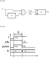
- the figure 1 is a diagram illustrating the operation of a PUF. When stimulated by a vector of data, called challenge C, the PUF generates an R response which is unique and which depends on the intrinsic manufacturing characteristics of the circuit.
- the different functionalities of a PUF can be achieved using devices that are more or less secure or costly in terms of performance / consumption / surface area, for example: fuses, secure memory with scrambling and encryption, set of sensors and devices for detecting attempts to read the secrets of the integrated circuit through physical access (reverse engineering), etc.
- PUFs are well known from the prior art and make it possible to measure one or more parameters (transistor threshold voltage, resistance of a metal line, parasitic capacitance, etc.) linked to the manufacture of circuits. integrated, which are likely to uniquely characterize each circuit.
- the implementation of the PUF function comprises a step consisting in measuring, by means of a TDC converter, the difference between: - i ) the instant of arrival of a first event of a signal at an input of the TDC converter and, - ii) the instant of arrival of a second event of a signal at an input of the TDC converter, which second event is generated by the delay circuit.
- This type of solution reveals a certain determinism in the response of the PUF.
- This determinism stems in particular from variations brought by the propagation paths between the source of the activation signal and the TDC, which variations influence the uniqueness of the single datum (or response) generated by the PUF.
- the unique data (or responses) generated by several integrated circuits embedding this same PUF can then present a certain correlation conducive to attacks.
- An objective of the invention is to remedy all or part of the aforementioned drawbacks.
- the invention makes it possible to generate the unique data specific to the circuit, in an optimum manner, in particular in terms of speed and energy consumption.
- the propagation time of identical signals, except for manufacturing variations, is measured very precisely, through one or more delay circuits.
- the propagation time differences in the delay circuit or circuits make it possible in particular to construct a signature or another unique identifier of the circuit.
- the invention is based on the measurement of delays in order to characterize and identify the integrated circuit.
- a direct measurement of the delays is carried out and not a frequency measurement.
- the direct measurement of the delay is done using a TDC, without passing through the frequency domain.
- the use of a very precise TDC is possible with a cost in surface and a reasonable consumption.
- This measurement is precise and fast (approximately 10 ns) and therefore makes it possible to gain one or two orders of magnitude on the latency of the other PUFs and in particular of the RO-PUFs.
- the invention also makes it possible to obtain stable measurements. Indeed, thanks to the rapid measurements of the delays, they are less subject to temperature variations, and more generally, are less sensitive to the conditions of use of the integrated circuit.
- Yet another aspect of the invention relates to the use of the integrated circuit to generate a random number.
- the method and the system which are the subject of the invention generate manipulations of physical elements, in particular signals (electrical or magnetic) and data, capable of being stored, transferred, combined, compared, etc., and making it possible to achieve a desired result.
- unique data specific to the integrated circuit and which is generated according to the method which is the subject of the invention, can in particular be understood as: a unique identifier, a unique signature, an intrinsic characteristic of the integrated circuit, a response to a challenge, etc. . These terms are equivalent and can be used interchangeably in the present description.
- the implementation of the method which is the subject of the invention involves the use of a “delay circuit” of the integrated circuit.
- This term includes in particular any propagation path in the circuit, which may be made up of passive (resistors, capacitors, inductors, etc.), active (transistors, diodes, etc.), complex (optoelectronic, electromechanical devices, etc.) elements. ) or any assembly of these elements through one or more standard logic cells.
- This delay circuit is a source of entropy serving as a source for "fixing" the variability of the manufacturing process and can be constructed in various ways. The differences in the propagation delays of a signal may result from variations in the manufacture of different elements of the integrated circuit.
- the choice of the delay circuit depends in particular on the technology used. To increase the efficiency of the process and decrease the size of the delay circuits, it is advantageous to maximize the variability / delay ratio.
- the implementation of the method which is the subject of the invention also involves the use of a TDC to extract / measure the entropy of the delay circuit.
- TDC To extract / measure the entropy of the delay circuit.
- the TDC is used to measure the time between two events. These events can be generated in the form of electrical signals by different types of generators: ring oscillators, pulse generator, etc. In the remainder of the description, the events to be analyzed correspond to rising and / or falling edges. The invention however covers other types of events, for example one or more pieces of information (eg number, letter, code, etc.) integrated into a signal. The TDC then measures the difference between the times of arrival of this information.
- the TDC does not give the time / time of arrival of each edge, but rather performs a measurement of the spacing between the two edges. In other words, the TDC does not compare arrival times of two events, but times the arrival difference between these two events. This eliminates the need to use a reference (or common clock) during the measurement. It is however possible to use a TDC which retrieves the arrival time of each event ("timestamp" in English) in relation to a reference clock (internal to the PUF / TDC, to the system, or external) then to make the subtraction of the two values to obtain the value of the measured delay.
- the figure 2a is a block diagram illustrating a device for implementing a method not covered by the claims, according to a first embodiment.
- the device has a CR delay circuit and a TDC. These elements allow the implementation of the PUF function of the integrated circuit.
- the TDC has two inputs: Start and Stop.
- An activation signal I is applied to the Start input of the TDC. This signal I corresponds to a first signal. This same signal I is applied to the input of the delay circuit CR.
- the Stop input of the TDC is connected to the output of the delay circuit CR.
- signal I has a rising edge fm 0 .
- This rising edge fm 0 corresponds to the first event whose arrival time is measured by the TDC (at the Start input) .
- the circuit CR induces a delay in the signal I so that the rising edge will arrive with a delay D at the level of the Stop input of the TDC.
- This rising edge fm 1 generated by the circuit CR corresponds to the second event whose time of arrival is measured by the TDC (at the Stop input) .
- the delayed signal at the output of the delay circuit CR corresponds to a second signal.
- the TDC will thus measure the delay D between the two rising edges - or the difference in the times of arrival of said rising edges ⁇ (fm 1 ; fm 0 ).
- the value of this delay D depends on the manufacturing characteristics intrinsic to the delay circuit CR and therefore of the integrated circuit.
- the embodiment of the figure 3a is similar to that of the figure 2a .
- the delay circuit CRi is however configured to invert the signal I (inverting delay; active on the rising edge of the activation signal I).
- the signal at the output of the circuit CRi then comprises a falling edge fd 1 which is delayed with respect to the rising edge fm 0 .
- the TDC will then measure the delay D between the rising edge fm 0 (first event of the first activation signal I arriving at the Start input) and the falling edge fd 1 (second event of the delayed signal arriving at the Stop input) - or the difference between the arrival times of the rising edge fm 0 and the falling edge fd 1 .
- the Start input of the TDC is active on a rising edge and the Stop input active on a falling edge.
- the signal I could include a falling edge instead of the rising edge and that the TDC measures the instants of arrival of a falling edge at the Start input and a rising edge at the Stop input.
- an AND logic gate is interposed between the TDC and the delay circuit CRi.
- Signal I is applied to an input of the AND gate.
- the other input of the AND gate is connected to the output of the delay circuit CRi.
- the output of the AND gate is connected to the Start and Stop TDC.
- the delay circuit CRi is configured to invert the signal I (inverter delay).
- the combination of the AND gate and the delay circuit CRi then makes it possible to generate a pulse - or signal referenced " Mre " - having a rising edge fm 0 and a falling edge fd 1 (single pulse generator or single pulse generator) .
- the TDC measures the pulse width of the Pulse signal, i.e. the delay D between the rising edge fm 0 (first event of the Pulse signal arriving at the Start input) and the falling edge fd 1 (second event of the same Pulse signal arriving at the Stop input) of the Pulse signal - or the difference between the arrival times of the rising edge fm 0 and the falling edge fd 1 .
- the Start input of the TDC is active on a rising edge and the Stop input active on a falling edge.
- the signal I could include a falling edge instead of the rising edge and that the TDC measures the instants of arrival of a falling edge at the Start input and a rising edge at the Stop input.
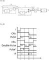
- the embodiment of the figure 5a corresponds to that of the figure 4a , the AND gate being however replaced by an exclusive NOR gate (XNOR gate).
- the activation signal I is a signal having a rising edge fm 0 and a falling edge fd 0 which succeeds it (the reverse being possible).
- the rising edge fm 0 is transformed into a falling edge fd 1
- the falling edge fd 0 is transformed into a rising edge fm 1 .
- the combination of XNOR gate and CRi delay circuit generates a double pulse - or Double Pulse signal (double pulse or double pulse generator). Each pulse has the same width and has a rising edge and a falling edge.
- the measurement performed by the TDC in the configuration of the figure 5a is more stable. Indeed, the redundancy of the measured values (width of two pulses greater than the width of a single pulse) makes it possible to increase the signal-to-noise ratio.
- signal I is applied to an input of an AND gate.
- the output of the AND gate is connected on the one hand to the input of the delay circuit CRi (inverter delay) and on the other hand to the Start and Stop inputs of the TDC.
- the output of the delay circuit CRi is connected to the other input of the AND gate.
- the combination of the AND gate and the delay circuit Cri usually called a ring oscillator, then makes it possible to generate multiple pulses - or Multi-Pulse signal - each having the same width and having a rising edge and a falling edge (generator multi-pulse).
- the TDC measures the width of each positive pulse of the Multi-Pulse signal, i.e. the delay D between a rising edge (first event of the Multi-Pulse signal arriving at the Start input) and the following falling edge ( second event of the same Multi-Pulse signal arriving at the Stop input) - or the difference between the arrival times of the rising edge and the falling edge of each pulse at the high state. If the TDC is not reset between two successive high pulses, the value of its measurement (R) corresponds to the sum of the widths of these successive high pulses, or to the sum of the half-periods of oscillation of the Multi-Pulse signal. . The redundancy of the measured values further increases the signal-to-noise ratio and the stability of the TDC measurement.
- the unique identifier R (calculated according to the modes of figures 2a to 6a ), can be compared to a reference value.
- the latter is preferably a fixed, invariable value, and does not depend on the conditions of use of the circuit such as the temperature.
- the reference value is for example calculated theoretically (a priori), or estimated from the measurement of numerous samples (mean value).
- a comparator can be integrated into the integrated circuit so that the comparison is carried out in situ, the reference value being stored in a memory of said circuit.
- the comparator can also be located outside the integrated circuit, in which case the comparison is carried out ex-situ, the reference value being stored in a remote memory of said circuit. This comparison can in particular be used in the context of monitoring and / or controlling manufacturing processes.
- the result of the comparison makes it possible, for example, to characterize the quality of the manufacture of the integrated circuit and to deduce therefrom the compensations necessary to make said circuit operate optimally (adjustment of the voltage or of the frequency for example).
- In situ comparison is used in this case.
- the result of the ex-situ comparison can be used to classify and sort the integrated circuits (eg: fast circuits or not) during manufacture, for example to sell them as different products, guaranteeing different performance.
- the device comprises several pulse generators G1, G2, ..., Gn (n being an integer equal to or greater than 2).
- These generators can be of the same type or of different types: single pulse generator (s) of the type shown on figure 4a ; double pulse generator (s) of the type shown in figure 5a ; multi-pulse generator (s) of the type shown in figure 6a , Or other.
- Each generator has a delay circuit so that the signal generated by a generator has a first event and a second event generated by said delay circuit.
- the inputs of the generators G1, G2, ..., Gn are connected to the outputs of a DEMUX demultiplexer.
- the outputs of the generators G1, G2, ..., Gn are connected to the inputs of a multiplexer MUX.
- the DEMUX demultiplexer makes it possible to inject the activation signal I into one of the generators G1, G2, ..., Gn selected.
- This demultiplexer is however optional, the activation signal I being able to be injected simultaneously into each of the generators G1, G2, ..., Gn.
- This activation signal I is of the type described above.
- the MUX multiplexer sends the signal generated by the selected generator to the Start and Stop inputs of the TDC. Depending on its form, this signal includes one or more first events (eg: rising edges) and one or more second events (eg: falling edges).
- the TDC measures the differences in the arrival times of these events. By successively selecting all or part of the other generators G1, G2, ..., Gn, the TDC will be able to successively measure several delays D1, D2, ..., Dn which are successively transmitted to a functional block B. This is suitable for constructing a response R from one or more of these measures (2, 3, 4, ..., n).
- This response R is appreciably more complex and more robust to attacks than those obtained according to the preceding embodiments. It can for example be constructed by a mathematical operation applied to the measured delays D1, D2, ..., Dn: addition of the delays, comparison of said delays between them (who is the fastest?), Subtraction of said delays (what is the difference propagation time of two delays?), comparison or subtraction of said delays from a reference value, division of said delays (what is the relationship between two delays?); or by a mathematical function with several variables applied to said measured delays.
- the data generated by block B is particularly suitable for the identification and / or authentication of electronic equipment, the secure storage of encryption keys, hardware-software coupling, the fight against counterfeiting, etc. Indeed, the data R can be expressed on several bits, becoming in fact more secure (unpredictable and non-reproducible).
- the results of the mathematical operation applied to the successive measured delays D1, D2, ..., Dn can in particular be concatenated to construct a unique proper datum on a number of bits necessary for an application (for example 128 bits for an AES encryption key , 2048 bits for RSA encryption).
- the measurements made by the TDC may depend on the conditions of use of the circuit (for example the temperature or the supply voltage).
- the comparison of two measurements will make it possible to cancel out the variations induced by the conditions of use. This eliminates the need for any means of compensation or analysis of these variations induced by the conditions of use.
- the embodiment of the figure 8 is similar to that of the figure 7 .
- the TDC has several inputs / outputs making it possible to simultaneously measure several delays D1, D2, ..., Dn and to transmit these measurements simultaneously to the functional block B.
- the latter has several inputs for this purpose.
- the measurements carried out by the TDC are in fact faster, because they are simultaneous.
- block B can process the various measurements simultaneously and no longer successively, and therefore generate a response R more rapidly.
- This embodiment is also less sensitive to the conditions of use, since the measurements are made simultaneously.
- the TDC makes it possible to measure propagation times in each delay circuit. This measurement does not need to be absolute. It is therefore possible to simplify the TDC so as to obtain a relative value for each measurement. It is also possible to recover only a modulo or other part of the measurement (by applying, for example, filtering of the least significant bits). This makes it possible to simplify the structure of the TDC to reduce its consumption and its surface, while maintaining good entropy in the responses of the PUF.
- the device then becomes not only an identifier generator (PUF) but also a random number generator (TRNG).
- PAF identifier generator
- TRNG random number generator
- the signal to noise ratio is then increased. For example, it is possible to make the signal travel several times through the same delay circuit before taking the measurement by the TDC. This makes it possible to reduce the impact of noise on the measurement. Indeed, the signal to noise ratio changes in ⁇ N (N being the number of times that the same delay circuit is traversed by the signal).
- FIG. 9a to 11 Other embodiments using a "shaping" block are illustrated in the figures 9a to 11 . It is likely that a rising edge and a falling edge do not propagate at the same speed in the integrated circuit. Thus, the more the activation signal I is generated at a distance from the TDC, the more the generated pulse will reduce or increase in width. There is therefore a risk of introducing a direct correlation between the selected source and the response obtained (between the challenge and the response), so that an attacker can more easily predict the signature of the integrated circuit. Also, an MF shaping block is advantageously used to overcome this state of affairs.
- a first single pulse generator G1 of the type described with reference to figure 4a , is used to generate a single pulse - Pulse signal - with a rising edge fm 0 and a falling edge fd 0 .
- a second double pulse generator G2 of the type described with reference to figure 5a , transforms the Pulse signal into a double pulse - Double Pulse signal. Each pulse exhibiting a rising edge fm 1 , respectively fm 2 , and a falling edge fd 1 , respectively fd 2 .
- the MF block is installed upstream of the TDC and connected to the inputs of the latter.
- the MF block is suitable for transforming the double pulse into a single pulse - Pulse 'signal.
- the block MF can in particular be active on the rising edges fm 1 , fm 2 (or falling edges fd 1 , fd 2 ).
- This transformation can for example be carried out by means of a flip-flop mounted as a divider, so as to pass only the rising edges (respectively falling) while reversing the even edges: the rising edge fm 1 is transmitted normally (this is the first event of which the arrival time is measured by the TDC), the following rising edge fm 2 is inverted to be transformed into a falling edge (this is the second event whose arrival time is measured by the TDC). And so on.
- a multi-pulse generator G allows to generate multiple pulses - Multi-Pulse signal.
- the MF block is active on the rising (or falling) edges, so as to pass only the rising edges (respectively falling) while inverting the even edges ( Multi-Pulse 'signal).
- Each pulse of the Multi-Pulse ' signal has a rising edge (first event whose arrival time is measured by the TDC) and a falling edge (second event whose arrival time is measured by the TDC). This falling edge results from the transformation of a rising edge as explained previously.
- the figure 11 schematizes an architecture similar to that of the figure 7 , but where the MF block is installed between the MUX multiplexer and the TDC.
- Each of the generators G1, G2, ..., Gn generates a signal in the form of a double pulse or multiple pulses.
- the MF block transforms each signal so that it presents one or more first events (eg: rising edges) and one or more second events (eg: falling edges) whose arrival times will be measured by the TDC.
- the times D1, D2, ..., Dn thus measured are then transmitted successively to the functional block B, the data R being generated in the same way as that described with reference to the figure 7 .
- the figure 12 schematizes an architecture similar to that of the figure 8 .
- Each TDC entry is however associated with a formatting block MF1, MF2, ..., MFn.
- Each signal (double pulse or multiple pulses) at the output of the multiplexer MUX is then transformed beforehand before entering the TDC.
- Each block MF1, MF2, ..., MFn transforms the corresponding signal so that it presents one or more first events (ex: edges amounts) and one or more second events (eg: falling edges) whose arrival times will be measured by the TDC.
- the times D1, D2, ..., Dn thus measured are then transmitted simultaneously to the functional block B, the data R being generated in the same way as that described with reference to the figure 8 .
- the shaping of the signal by the MF block, before its measurement by the TDC makes it possible to cancel, or at the very least to limit, any determinism in the response of the signal. PUF. All the variations brought about by the propagation paths between the source of the activation signal I and the TDC are common to all the sources / challenges and do not influence the uniqueness of the response R. The latter is then more stable and more robust to attacks.
- the TDC measures positive pulses.
- the TDC can be configured to measure negative pulses.
- one or more characteristics and / or steps exposed only in one embodiment can be generalized to the other embodiments.
- one or more features and / or steps disclosed only in one embodiment may be combined with one or more other features and / or steps disclosed only in another embodiment.
Abstract
L'invention concerne un procédé pour générer une donnée unique (R) propre à un circuit intégré en silicium, ladite donnée étant générée par l'application d'une fonction physiquement non clonable PUF dudit circuit, lequel circuit comporte un circuit de retard (CR, CRi), la mise en œuvre de la fonction PUF comprend une étape consistant à mesurer, au moyen d'un convertisseur TDC, la différence entre :- l'instant d'arrivée d'un premier événement d'un signal à une entrée (Start) du convertisseur TDC et,- l'instant d'arrivée d'un second événement d'un signal à une entrée (Stop) du convertisseur TDC, lequel second événement est généré par le circuit de retard (CR).The invention relates to a method for generating a single datum (R) specific to a silicon integrated circuit, said datum being generated by the application of a physically unclonable function PUF of said circuit, which circuit comprises a delay circuit (CR , CRi), the implementation of the PUF function comprises a step consisting in measuring, by means of a TDC converter, the difference between: - the arrival time of a first event of a signal at an input (Start) of the TDC converter and, - the instant of arrival of a second event of a signal at an input (Stop) of the TDC converter, which second event is generated by the delay circuit (CR).
Description
L'invention concerne un procédé pour générer une donnée unique propre à un circuit intégré en silicium. Elle concerne également un circuit intégré ainsi qu'une utilisation spécifique de ce circuit.The invention relates to a method for generating unique data specific to a silicon integrated circuit. It also relates to an integrated circuit as well as a specific use of this circuit.
Le domaine de l'invention concerne notamment la sécurisation des circuits intégrés, et l'identification et/ou l'authentification de composants électroniques.The field of the invention relates in particular to the securing of integrated circuits, and the identification and / or authentication of electronic components.
Le processus de fabrication d'un circuit intégré en silicium entraine obligatoirement de petites variations entre les circuits. Ces variations se traduisent par exemple par la propagation plus ou moins longue des signaux électriques à l'intérieur du circuit. Aussi, il est avantageux de pouvoir caractériser de manière unique un circuit parmi une série de circuits issus de la même chaine de fabrication. Cette identification peut être réalisée grâce à une caractéristique physique intrinsèque au circuit intégré extraite par l'application d'une fonction physiquement non clonable PUF (pour l'acronyme anglais « Physically Unclonable Function »). Cette caractéristique est l'équivalent d'une empreinte digitale propre au circuit et peut notamment être utilisée pour l'identification et/ou l'authentification de matériel électronique, le stockage sécurisé de clés de chiffrement, un couplage matériel-logiciel, la lutte contre la contrefaçon, etc. La
Les différentes fonctionnalités d'une PUF peuvent être réalisées à l'aide de dispositifs plus ou moins sécurisés ou coûteux en termes de performance/consommation/surface, par exemple : fusibles, mémoire sécurisé avec brouillage (scrambling en anglais) et chiffrement, ensemble de capteurs et de dispositifs permettant de détecter des tentatives de lecture des secrets du circuit intégré au travers d'accès physique (ingénierie inverse), etc.The different functionalities of a PUF can be achieved using devices that are more or less secure or costly in terms of performance / consumption / surface area, for example: fuses, secure memory with scrambling and encryption, set of sensors and devices for detecting attempts to read the secrets of the integrated circuit through physical access (reverse engineering), etc.
D'autre part, les PUF sont bien connues de l'art antérieur et permettent de mesurer un ou plusieurs paramètres (tension de seuil de transistor, résistance d'une ligne de métal, capacité parasite...) liés à la fabrication des circuits intégrés, qui sont susceptibles de caractériser de manière unique chaque circuit.On the other hand, PUFs are well known from the prior art and make it possible to measure one or more parameters (transistor threshold voltage, resistance of a metal line, parasitic capacitance, etc.) linked to the manufacture of circuits. integrated, which are likely to uniquely characterize each circuit.
Des PUF sont notamment décrites dans les documents brevets
Ces PUF connues de l'art antérieur présentent un certain nombre d'inconvénients :
- Latence significative en lecture, pour les PUF dit dynamiques (mesure d'un paramètre électrique - courant, résistance, ... - qui n'est a priori pas observable statiquement). Dans ce cas, les mesures sont souvent imprécises et bruitées. Elles sont assez longues (de l'ordre de la microseconde) et doivent être répétées de nombreuses fois et moyennées pour être assez stables.
- Surconsommation d'énergie électrique, liée à la nécessité d'ajouter du matériel de post-traitement et/ou de correction d'erreurs pour obtenir des mesures stables, quelles que soient les conditions d'opération (tension et température).
- Surface, ou taille du circuit, importante (donc plus chère et avec une consommation énergétique plus importante), due à la faible efficacité d'extraction de l'information des sources de variabilité utilisées. Dans ce cas, il faut multiplier le nombre de sources pour atteindre le nombre de bits voulus pour la clé de chiffrement ou l'identifiant.
- Vulnérabilité aux attaques physiques d'ingénierie inverse. Certaines PUF utilisent des structures « statiques » (par exemple : probabilité de fabrication correcte d'un via - trou métallisé qui permet d'établir une liaison électrique entre deux couches). Mais ces structures sont visibles et peuvent donc être copiées facilement. D'autres PUF utilisent l'état initial d'une mémoire comme source d'entropie (chaque bit de la mémoire se stabilise à 0 ou 1, un certain temps après la mise sous tension du circuit ; cet état du plan mémoire au démarrage est caractéristique de chaque mémoire et donc de chaque circuit). Lorsque le circuit est éteint, le secret n'est pas lisible, car il est caché dans la nanostructure des transistors qui composent la mémoire. Mais dès lors que la mémoire est alimentée, le secret est automatiquement extrait et est stocké électriquement dans la mémoire. Il devient plus facilement accessible (« lisible ») à un attaquant possédant l'outillage nécessaire (par exemple, attaque à l'aide de laser).
- Vulnérabilité aux attaques dites par canaux cachés. Ces attaques consistent à observer le comportement du circuit intégré et à exploiter les informations qu'il émet sur des canaux auxiliaires (consommation électrique, rayonnement électromagnétique, temps de calcul...) pour en déduire les secrets qu'il manipule. Les temps de mesures importants pour les PUF classiques augmentent la largeur de la fenêtre d'attaque.
- Significant reading latency, for so-called dynamic PUFs (measurement of an electrical parameter - current, resistance, etc. - which is not a priori statically observable). In this case, the measurements are often imprecise and noisy. They are quite long (of the order of a microsecond) and must be repeated many times and averaged to be fairly stable.
- Overconsumption of electrical energy, linked to the need to add post-processing and / or error correction equipment to obtain stable measurements, whatever the operating conditions (voltage and temperature).
- Large surface area, or size of the circuit (therefore more expensive and with greater energy consumption), due to the low efficiency of extracting information from the sources of variability used. In this case, the number of sources must be multiplied to reach the desired number of bits for the encryption key or the identifier.
- Vulnerability to physical reverse engineering attacks. Some PUFs use “static” structures (for example: probability of correct fabrication of a metallized via-hole which makes it possible to establish an electrical connection between two layers). But these structures are visible and can therefore be copied easily. Other PUFs use the initial state of a memory as a source of entropy (each bit of the memory stabilizes at 0 or 1, a certain time after the circuit is powered up; this state of the memory plane at startup is characteristic of each memory and therefore of each circuit). When the circuit is off, the secret cannot be read because it is hidden in the nanostructure of the transistors that make up the memory. But as soon as the memory is powered, the secret is automatically extracted and is stored electrically in the memory. It becomes more easily accessible ("readable") to an attacker with the necessary tools (eg laser attack).
- Vulnerability to so-called hidden channel attacks. These attacks consist in observing the behavior of the integrated circuit and in exploiting the information that it transmits on auxiliary channels (electrical consumption, electromagnetic radiation, calculation time, etc.) to deduce the secrets that it manipulates. The long measurement times for conventional PUFs increase the width of the attack window.
La mise en œuvre des PUF se base généralement sur l'analyse de variations de délais pour caractériser et identifier le circuit. On utilise couramment une mesure de la fréquence (nombre d'événements sur une période donnée) de différents oscillateurs. On parle souvent de RO-PUF (pour l'acronyme anglais « Ring Oscillator » PUF). Cette mesure en fréquence, pour être précise, nécessite de comptabiliser le nombre d'événements sur une longue période. La latence de réponse est donc élevée. Pour être stables, ces mesures doivent aussi être différentielles (entre deux oscillateurs) et faire une comparaison simple (quel est l'oscillateur le plus rapide ?). Au final ces solutions demandent donc au minimum deux oscillateurs pour extraire un seul bit d'entropie (des solutions avec 4 ou 8 oscillateurs par bit sont même envisagées pour augmenter la stabilité des mesures).The implementation of PUFs is generally based on the analysis of variations in delays to characterize and identify the circuit. A measure of the frequency (number of events over a given period) of different oscillators is commonly used. We often speak of RO-PUF (for the English acronym "Ring Oscillator" PUF). This frequency measurement, to be precise, requires counting the number of events over a long period. The response latency is therefore high. To be stable, these measurements must also be differential (between two oscillators) and make a simple comparison (which is the fastest oscillator?). In the end, these solutions therefore require at least two oscillators to extract a single entropy bit (solutions with 4 or 8 oscillators per bit are even considered to increase the stability of the measurements).
On connait par le document brevet
Un objectif de l'invention est de remédier à tout ou partie des inconvénients précités.An objective of the invention is to remedy all or part of the aforementioned drawbacks.
La solution proposée par l'invention est un procédé pour générer une donnée unique propre à un circuit intégré en silicium, ladite donnée étant générée par l'application d'une fonction physiquement non clonable PUF dudit circuit, lequel circuit comporte également un circuit de retard. La mise en œuvre de la fonction PUF comprend une étape consistant à mesurer, au moyen d'un convertisseur de temps numérique (ci-après « TDC » pour l'acronyme anglais Time-to-digital converter), la différence entre :
- i) l'instant d'arrivée d'un premier évènement d'un signal à une entrée du TDC et,
- ii) l'instant d'arrivée d'un second événement d'un signal à une entrée du TDC, le second événement étant généré par le circuit de retard.
- i) the time of arrival of a first event of a signal at an input of the TDC and,
- ii) the instant of arrival of a second event of a signal at an input of the TDC, the second event being generated by the delay circuit.
Le procédé comprend en outre les étapes supplémentaires consistant à :
- générer, au moyen d'au moins un générateur comportant le circuit de retard, un signal sous la forme d'une double impulsion ou de multiples impulsions,
- transformer ledit signal de manière à ce que le premier événement et le second événement appartiennent audit signal transformé
- generating, by means of at least one generator comprising the delay circuit, a signal in the form of a double pulse or of multiple pulses,
- transforming said signal so that the first event and the second event belong to said transformed signal
L'invention permet de générer la donnée unique propre au circuit, de manière optimale, notamment en termes de rapidité et de consommation d'énergie. On mesure de façon très précise le temps de propagation de signaux identiques aux variations de fabrication près, au travers d'un ou plusieurs circuits de retard. Les différences de temps de propagation dans le ou les circuits de retards permettent notamment de construire une signature ou un autre identifiant unique du circuit.The invention makes it possible to generate the unique data specific to the circuit, in an optimum manner, in particular in terms of speed and energy consumption. The propagation time of identical signals, except for manufacturing variations, is measured very precisely, through one or more delay circuits. The propagation time differences in the delay circuit or circuits make it possible in particular to construct a signature or another unique identifier of the circuit.
L'invention se base sur la mesure de délais pour caractériser et identifier le circuit intégré. On réalise une mesure directe des délais et non pas une mesure de fréquence. La mesure directe du délai se fait à l'aide d'un TDC, sans passage par le domaine fréquentiel. L'utilisation d'un TDC très précis est possible avec un coût en surface et une consommation raisonnable. Cette mesure est précise et rapide (environ 10 ns) et permet donc de gagner un ou deux ordres de grandeur sur la latence des autres PUF et notamment des RO-PUF.The invention is based on the measurement of delays in order to characterize and identify the integrated circuit. A direct measurement of the delays is carried out and not a frequency measurement. The direct measurement of the delay is done using a TDC, without passing through the frequency domain. The use of a very precise TDC is possible with a cost in surface and a reasonable consumption. This measurement is precise and fast (approximately 10 ns) and therefore makes it possible to gain one or two orders of magnitude on the latency of the other PUFs and in particular of the RO-PUFs.
Il est aussi possible d'extraire plusieurs bits d'entropie à chaque mesure. En effet, le résultat de la comparaison entre deux délais ne sera pas binaire (qui est le plus grand des deux délais ?), mais pourra être exprimé sur plusieurs bits en calculant la différence entre deux délais. Ainsi un nombre de circuits de retard moins important permet d'extraire un même nombre de bits. On peut donc réduire la surface de la PUF par un facteur deux ou trois, et de fait réduire la taille du circuit intégré.It is also possible to extract several entropy bits for each measurement. Indeed, the result of the comparison between two delays will not be binary (which is the larger of the two delays?), But can be expressed over several bits by calculating the difference between two delays. Thus, a smaller number of delay circuits makes it possible to extract the same number of bits. It is therefore possible to reduce the surface area of the PUF by a factor of two or three, and in fact reduce the size of the integrated circuit.
L'invention permet en outre d'obtenir des mesures stables. En effet, grâce aux mesures rapides des délais, celles-ci sont moins sujettes aux variations de température, et de manière plus générale, sont moins sensibles aux conditions d'utilisation du circuit intégré.The invention also makes it possible to obtain stable measurements. Indeed, thanks to the rapid measurements of the delays, they are less subject to temperature variations, and more generally, are less sensitive to the conditions of use of the integrated circuit.
De plus, du fait de la mesure directe des délais, les risques de fuites d'information par attaques par canaux cachés sont très réduits. Il est donc plus difficile à une personne malveillante de retrouver l'information cachée dans le circuit intégré en observant celui-ci de manière non intrusive. Cela n'est pas le cas pour les solutions classiques dans lesquelles la durée de mesure importante expose le rayonnement électromagnétique et la consommation des sources d'entropie (oscillateurs) pendant plus longtemps.In addition, due to the direct measurement of delays, the risks of information leaks by hidden channel attacks are very reduced. It is therefore more difficult for a malicious person to find the information hidden in the integrated circuit by observing it in a non-intrusive manner. This is not the case for conventional solutions in which the long measurement time exposes electromagnetic radiation and the consumption of entropy sources (oscillators) for a longer time.
Enfin, la génération d'un signal double impulsion ou multiples impulsions, combinée à la transformation dudit signal, permet d'annuler, ou à tout le moins de limiter, tout déterminisme dans la réponse du PUF. Toutes les variations amenées par les chemins de propagation entre la source du signal d'activation et le TDC sont communes à toutes les sources/challenges et n'influent pas sur l'unicité de la réponse. Cette dernière est alors plus robuste aux attaques. En propageant plusieurs impulsions dans le circuit, on s'affranchit des problèmes de déformation lié à la propagation, notamment de la distance entre les sources/challenges et le TDC qui peuvent impacter les réponses du PUF (impact sur la "randomness"). Cet impact est accentué lorsque la taille de la banque d'entropie augmente (le nombre de générateurs). Grâce à l'apport de l'invention, on vient sélectionner, au niveau du TDC (une fois que la distance est « parcourue »), les deux fronts qui vont définir le début et la fin de la mesure.Finally, the generation of a double-pulse or multiple-pulse signal, combined with the transformation of said signal, makes it possible to cancel, or at the very least to limit, any determinism in the response of the PUF. All the variations brought about by the propagation paths between the source of the activation signal and the TDC are common to all the sources / challenges and do not influence the uniqueness of the response. The latter is then more robust to attacks. By propagating several pulses in the circuit, one overcomes the problems of deformation linked to propagation, in particular of the distance between the sources / challenges and the TDC which can impact the responses of the PUF (impact on "randomness"). This impact is accentuated when the size of the entropy bank increases (the number of generators). Thanks to the contribution of the invention, one comes to select, at the level of the TDC (once the distance is “covered”), the two edges which will define the start and the end of the measurement.
D'autres caractéristiques avantageuses de l'invention sont listées ci-dessous. Chacune de ces caractéristiques peut être considérée seule ou en combinaison avec les caractéristiques du procédé définies ci-dessus (notamment les caractéristiques supplémentaires), et faire l'objet, le cas échéant, d'une ou plusieurs demandes de brevet divisionnaires :
- Selon un mode de réalisation non couvert par les revendications, le premier événement appartient à un premier signal et le second événement appartient à un second signal, lequel second signal est pris à la sortie du circuit de retard à l'entrée duquel est appliqué le premier signal.
- Selon un mode de réalisation non couvert par les revendications, le premier événement et le second événement appartiennent à un même signal, lequel signal est généré par un générateur d'impulsions comportant le circuit de retard.
- Selon un mode de réalisation non couvert par les revendications, le circuit intégré comporte plusieurs circuits de retard, ledit procédé comprenant les étapes consistant à : - a) former une pluralité de générateurs d'impulsions, chaque générateur comportant un desdits circuits de retard, de sorte que le signal généré par ledit générateur présente un premier événement et un second événement généré par ledit circuit de retard ; - b) sélectionner, parmi la pluralité des générateurs, un premier générateur et générer un premier signal depuis ledit premier générateur ; - c) mesurer, au moyen du convertisseur TDC, la différence entre l'instant d'arrivée du premier évènement du premier signal et, l'instant d'arrivée du second évènement dudit premier signal ; - d) réitérer les étapes a) à c) pour tout ou partie des autres générateurs ; - e) générer la donnée unique propre au circuit intégré, en fonction d'une ou plusieurs des mesures successives du convertisseur TDC.
- Selon un mode de réalisation, le circuit intégré comporte plusieurs circuits de retard, ledit procédé comprenant les étapes consistant à : - a) former une pluralité de générateurs d'impulsions, chaque générateur comportant un desdits circuits de retard, le signal généré par chaque générateur se présentant sous la forme d'une double impulsion ou de multiples impulsions ; - b) sélectionner, parmi la pluralité des générateurs, un premier générateur et générer un premier signal depuis ledit premier générateur ; - b1) transformer ledit premier signal de manière à ce que le premier évènement et le second évènement appartiennent audit signal transformé ; - c) mesurer, au moyen du convertisseur TDC, la différence entre l'instant d'arrivée du premier évènement du premier signal transformé et, l'instant d'arrivée du second évènement dudit premier signal transformé ; - d) réitérer les étapes a) à c) pour tout ou partie des autres générateurs ; - e) générer la donnée unique propre au circuit intégré, en fonction d'une ou plusieurs des mesures successives du convertisseur TDC.
- Selon un mode de réalisation non couvert par les revendications, le circuit intégré comporte plusieurs circuits de retard, ledit procédé comprenant les étapes consistant à : - a) former une pluralité de générateurs d'impulsions, chaque générateur comportant un desdits circuits de retard, de sorte que le signal généré par ledit générateur présente un premier évènement et un second évènement généré par ledit circuit de retard ; - b) générer simultanément une pluralité de signaux depuis lesdits générateurs ; - c) mesurer, au moyen du convertisseur TDC, la différence entre l'instant d'arrivée du premier évènement d'un signal généré à l'étape b) et l'instant d'arrivée du second évènement dudit signal, laquelle mesure est réalisée simultanément pour la pluralité de signaux générés à l'étape b) ; - d) générer la donnée unique propre au circuit intégré, en fonction des mesures simultanées du convertisseur TDC.
- Selon un mode de réalisation le circuit intégré comporte plusieurs circuits de retard, ledit procédé comprenant les étapes consistant à : - a) former une pluralité de générateurs d'impulsions, chaque générateur comportant un desdits circuits de retard, le signal généré par chaque générateur se présentant sous la forme d'une double impulsion ou de multiples impulsions ; - b) générer simultanément une pluralité de signaux depuis lesdits générateurs ; - b1) transformer chaque signal de manière à ce que chaque signal transformé présente un premier évènement et un second événement ; - c) mesurer, au moyen du convertisseur TDC, la différence entre l'instant d'arrivée du premier évènement d'un signal transformé à l'étape b1) et l'instant d'arrivée du second évènement dudit signal transformé, laquelle mesure est réalisée simultanément pour la pluralité de signaux transformés à l'étape b1) ; - d) générer la donnée unique propre au circuit intégré, en fonction des mesures simultanées du convertisseur TDC.
- Selon un mode de réalisation, la donnée unique propre au circuit intégré est générée par une opération mathématique ou une fonction mathématique à plusieurs variables appliquée aux différentes mesures du convertisseur TDC.
- Selon un mode de réalisation, on fait parcourir plusieurs fois un signal au travers du circuit de retard avant de faire la mesure par le convertisseur TDC.
- According to an embodiment not covered by the claims, the first event belongs to a first signal and the second event belongs to a second signal, which second signal is taken at the output of the delay circuit to the input of which the first is applied. signal.
- According to an embodiment not covered by the claims, the first event and the second event belong to the same signal, which signal is generated by a pulse generator comprising the delay circuit.
- According to an embodiment not covered by the claims, the integrated circuit comprises several delay circuits, said method comprising the steps consisting in: a) forming a plurality of pulse generators, each generator comprising one of said delay circuits, of so that the signal generated by said generator has a first event and a second event generated by said delay circuit; - b) selecting, from among the plurality of generators, a first generator and generating a first signal from said first generator; c) measuring, by means of the TDC converter, the difference between the time of arrival of the first event of the first signal and the time of arrival of the second event of the said first signal; - d) repeating steps a) to c) for all or part of the other generators; - e) generating the unique data item specific to the integrated circuit, as a function of one or more of the successive measurements of the TDC converter.
- According to one embodiment, the integrated circuit comprises several delay circuits, said method comprising the steps of: a) forming a plurality of pulse generators, each generator comprising one of said delay circuits, the signal generated by each generator in the form of a double pulse or multiple pulses; - b) selecting, from among the plurality of generators, a first generator and generating a first signal from said first generator; - b1) transforming said first signal so that the first event and the second event belong to said transformed signal; c) measuring, by means of the TDC converter, the difference between the time of arrival of the first event of the first transformed signal and the time of arrival of the second event of said first transformed signal; - d) repeating steps a) to c) for all or part of the other generators; - e) generating the unique data item specific to the integrated circuit, as a function of one or more of the successive measurements of the TDC converter.
- According to an embodiment not covered by the claims, the integrated circuit comprises several delay circuits, said method comprising the steps consisting in: a) forming a plurality of pulse generators, each generator comprising one of said delay circuits, of so that the signal generated by said generator has a first event and a second event generated by said delay circuit; - b) simultaneously generating a plurality of signals from said generators; - c) measuring, by means of the TDC converter, the difference between the time of arrival of the first event of a signal generated in step b) and the time of arrival of the second event of said signal, which measurement is performed simultaneously for the plurality of signals generated in step b); - d) generate the unique data specific to the integrated circuit, as a function of the simultaneous measurements of the TDC converter.
- According to one embodiment, the integrated circuit comprises several delay circuits, said method comprising the steps of: a) forming a plurality of pulse generators, each generator comprising one of said delay circuits, the signal generated by each generator is presenting as a double pulse or multiple pulses; - b) simultaneously generating a plurality of signals from said generators; - b1) transforming each signal so that each transformed signal has a first event and a second event; - c) measuring, by means of the TDC converter, the difference between the instant of arrival of the first event of a signal transformed in step b1) and the instant of arrival of the second event of said transformed signal, which measures is carried out simultaneously for the plurality of signals transformed in step b1); - d) generate the unique data specific to the integrated circuit, as a function of the simultaneous measurements of the TDC converter.
- According to one embodiment, the single datum specific to the integrated circuit is generated by a mathematical operation or a mathematical function with several variables applied to the various measurements of the TDC converter.
- According to one embodiment, a signal is passed through the delay circuit several times before the measurement is taken by the TDC converter.
Un autre aspect de l'invention concerne un circuit intégré en silicium comportant une fonction physiquement non clonable PUF permettant de générer une donnée unique propre audit circuit, lequel circuit comporte :
- un circuit de retard,
- un convertisseur TDC pour la mise en œuvre de la fonction PUF, lequel convertisseur TDC est adapté pour mesurer :
- i) l'instant d'arrivée d'un premier évènement d'un signal à une entrée du convertisseur TDC et,
- ii) l'instant d'arrivée d'un second évènement d'un signal à une entrée du convertisseur TDC, lequel second évènement est généré par le circuit de retard.
- a delay circuit,
- a TDC converter for implementing the PUF function, which TDC converter is suitable for measuring:
- i) the instant of arrival of a first event of a signal at an input of the TDC converter and,
- ii) the time of arrival of a second event of a signal at an input of the TDC converter, which second event is generated by the delay circuit.
Ce circuit comporte en outre les caractéristiques supplémentaires suivantes :
- au moins un générateur comportant le circuit de retard, lequel générateur est adapté pour générer un signal sous la forme d'une double impulsion ou de multiples impulsions,
- un moyen pour transformer ledit signal de manière à ce que le premier évènement et le second évènement appartiennent audit signal transformé.
- at least one generator comprising the delay circuit, which generator is adapted to generate a signal in the form of a double pulse or of multiple pulses,
- means for transforming said signal so that the first event and the second event belong to said transformed signal.
Encore un autre aspect de l'invention concerne l'utilisation du circuit intégré pour générer un nombre aléatoire.Yet another aspect of the invention relates to the use of the integrated circuit to generate a random number.
D'autres avantages et caractéristiques de l'invention apparaîtront mieux à la lecture de la description d'un mode de réalisation préféré qui va suivre, en référence aux dessins annexés, réalisés à titre d'exemples indicatifs et non limitatifs et sur lesquels :
- [
Fig. 1 ] précité est un diagramme illustrant le fonctionnement d'une PUF, - [
Fig. 2a ] est un bloc-diagramme illustrant un dispositif pour la mise en œuvre d'un procédé, selon un premier mode de réalisation, - [
Fig. 2b ] est un diagramme de temps montrant la forme de signaux dans le dispositif de lafigure 2a , - [
Fig. 3a ] est un bloc-diagramme illustrant un dispositif pour la mise en œuvre d'un procédé, selon un deuxième mode de réalisation, - [
Fig. 3b ] est un diagramme de temps montrant la forme de signaux dans le dispositif de lafigure 3a , - [
Fig. 4a ] est un bloc-diagramme illustrant un dispositif pour la mise en œuvre d'un procédé, selon un troisième mode de réalisation, - [
Fig. 4b ] est un diagramme de temps montrant la forme de signaux dans le dispositif de lafigure 4a , - [
Fig. 5a ] est un bloc-diagramme illustrant un dispositif pour la mise en œuvre d'un procédé, selon un quatrième mode de réalisation, - [
Fig. 5b ] est un diagramme de temps montrant la forme de signaux dans le dispositif de lafigure 5a , - [
Fig. 6a ] est un bloc-diagramme illustrant un dispositif pour la mise en œuvre d'un procédé, selon un cinquième mode de réalisation, - [
Fig. 6b ] est un diagramme de temps montrant la forme de signaux dans le dispositif de lafigure 6a , - [
Fig. 7 ] est un bloc-diagramme illustrant un dispositif pour la mise en œuvre d'un procédé, selon un sixième mode de réalisation, - [
Fig. 8 ] est un bloc-diagramme illustrant un dispositif pour la mise en œuvre d'un procédé, selon un septième mode de réalisation, - [
Fig. 9a ] est un bloc-diagramme illustrant un dispositif pour la mise en œuvre d'un procédé, selon un huitième mode de réalisation, - [
Fig. 9b ] est un diagramme de temps montrant la forme de signaux dans le dispositif de lafigure 9a , - [
Fig. 10a ] est un bloc-diagramme illustrant un dispositif pour la mise en œuvre d'un procédé, selon un neuvième mode de réalisation, - [
Fig. 10b ] est un diagramme de temps montrant la forme de signaux dans le dispositif de lafigure 10a . - [
Fig. 11 ] est un bloc-diagramme illustrant un dispositif pour la mise en œuvre d'un procédé, selon un dixième mode de réalisation, - [
Fig. 12 ] est un bloc-diagramme illustrant un dispositif pour la mise en œuvre d'un procédé, selon un onzième mode de réalisation.
- [
Fig. 1 ] above is a diagram illustrating the operation of a PUF, - [
Fig. 2a ] is a block diagram illustrating a device for implementing a method, according to a first embodiment, - [
Fig. 2b ] is a timing diagram showing the shape of signals in the device of thefigure 2a , - [
Fig. 3a ] is a block diagram illustrating a device for implementing a method, according to a second embodiment, - [
Fig. 3b ] is a timing diagram showing the shape of signals in the device of thefigure 3a , - [
Fig. 4a ] is a block diagram illustrating a device for implementing a method, according to a third embodiment, - [
Fig. 4b ] is a timing diagram showing the shape of signals in the device of thefigure 4a , - [
Fig. 5a ] is a block diagram illustrating a device for implementing a method, according to a fourth embodiment, - [
Fig. 5b ] is a timing diagram showing the shape of signals in the device of thefigure 5a , - [
Fig. 6a ] is a block diagram illustrating a device for implementing a method, according to a fifth embodiment, - [
Fig. 6b ] is a timing diagram showing the shape of signals in the device of thefigure 6a , - [
Fig. 7 ] is a block diagram illustrating a device for implementing a method, according to a sixth embodiment, - [
Fig. 8 ] is a block diagram illustrating a device for implementing a method, according to a seventh embodiment, - [
Fig. 9a ] is a block diagram illustrating a device for implementing a method, according to an eighth embodiment, - [
Fig. 9b ] is a timing diagram showing the shape of signals in the device of thefigure 9a , - [
Fig. 10a ] is a block diagram illustrating a device for implementing a method, according to a ninth embodiment, - [
Fig. 10b ] is a timing diagram showing the shape of signals in the device of thefigure 10a . - [
Fig. 11 ] is a block diagram illustrating a device for implementing a method, according to a tenth embodiment, - [
Fig. 12 ] is a block diagram illustrating a device for implementing a method, according to an eleventh embodiment.
Le procédé et le système objets de l'invention engendrent des manipulations d'éléments physiques, notamment des signaux (électriques ou magnétiques) et des données, capables d'être stockés, transférés, combinés, comparés, ..., et permettant d'aboutir à un résultat souhaité.The method and the system which are the subject of the invention generate manipulations of physical elements, in particular signals (electrical or magnetic) and data, capable of being stored, transferred, combined, compared, etc., and making it possible to achieve a desired result.
Tel qu'utilisé ici, sauf indication contraire, l'utilisation des adjectifs ordinaux «premier», «deuxième», etc., pour décrire un objet indique simplement que différentes occurrences d'objets similaires sont mentionnées et n'implique pas que les objets ainsi décrits doivent être dans une séquence donnée, que ce soit dans le temps, dans l'espace, dans un classement ou de toute autre manière.As used herein, unless otherwise specified, the use of the ordinal adjectives "first", "second", etc., to describe an object simply indicates that different occurrences of similar objects are mentioned and does not imply that the objects thus described must be in a given sequence, whether in time, space, classification or in any other way.
La « donnée unique » propre au circuit intégrée et qui est générée selon le procédé objet de l'invention, peut notamment être comprise comme : un identifiant unique, une signature unique, une caractéristique intrinsèque du circuit intégré, une réponse à un challenge, etc. Ces termes sont équivalents et peuvent être utilisés indifféremment dans la présente description.The “ unique data ” specific to the integrated circuit and which is generated according to the method which is the subject of the invention, can in particular be understood as: a unique identifier, a unique signature, an intrinsic characteristic of the integrated circuit, a response to a challenge, etc. . These terms are equivalent and can be used interchangeably in the present description.
La mise en œuvre du procédé objet de l'invention implique l'utilisation d'un « circuit de retard » du circuit intégré. Ce terme englobe notamment tout chemin de propagation dans le circuit, pouvant être constitué d'éléments passifs (résistances, capacités, inductances...), actifs (transistors, diodes, ...), complexes (optoélectronique, dispositifs électromécaniques... ) ou tout assemblage de ces éléments au travers d'une ou plusieurs cellules logiques standards. Ce circuit de retard est une source d'entropie servant comme source de « fixation » de la variabilité du procédé de fabrication et pouvant être construit de diverses manières. Les différences de délais de propagation d'un signal peuvent résulter de variations de fabrication de différents éléments du circuit intégré. Ce sont notamment les variations de paramètres caractéristiques d'un ou plusieurs transistors utilisés dans le circuit de retard (variation de la longueur d'un canal, du dopage N, du dopage P, de la taille de la grille, de la tension de seuil...). Ces variations sont liées à la fabrication des couches les plus basses d'un circuit intégré (couches actives, oxyde, caissons...). La fabrication des couches de plus haut niveau (couches d'interconnexion et couches métal) peut également être sujette à des variations de fabrication. Il est donc envisageable d'utiliser des éléments résistifs (fils d'interconnexion) comme circuits de retard si ces éléments ont une variabilité plus importante que les transistors. Une combinaison de ces deux types de circuits de retard est aussi envisageable.The implementation of the method which is the subject of the invention involves the use of a “delay circuit” of the integrated circuit. This term includes in particular any propagation path in the circuit, which may be made up of passive (resistors, capacitors, inductors, etc.), active (transistors, diodes, etc.), complex (optoelectronic, electromechanical devices, etc.) elements. ) or any assembly of these elements through one or more standard logic cells. This delay circuit is a source of entropy serving as a source for "fixing" the variability of the manufacturing process and can be constructed in various ways. The differences in the propagation delays of a signal may result from variations in the manufacture of different elements of the integrated circuit. These are in particular the variations of characteristic parameters of one or more transistors used in the delay circuit (variation of the length of a channel, of the N doping, of the P doping, of the size of the gate, of the threshold voltage. ...). These variations are linked to the manufacture of the lowest layers of an integrated circuit (active layers, oxide, wells, etc.). The manufacture of higher level layers (interconnect layers and metal layers) may also be subject to manufacturing variations. It is therefore conceivable to use resistive elements (interconnection wires) as delay circuits if these elements have a greater variability than the transistors. A combination of these two types of delay circuits is also possible.
D'autres composants du circuit intégré qui contribuent aux variations de fabrication sont également envisageables. Par exemple la variation de la capacité d'une interconnexion résulte en une variation du temps de propagation au travers de celle-ci. Il est donc possible d'augmenter cette capacité avec des éléments susceptibles de varier lors de la fabrication pour créer les sources d'entropie (capacité MOS, MOM ou autre...).Other components of the integrated circuit which contribute to manufacturing variations are also possible. For example, the variation in the capacity of an interconnection results in a variation in the propagation time through it. It is therefore possible to increase this capacity with elements likely to vary during manufacture to create the sources of entropy (MOS, MOM or other capacity, etc.).
Le choix du circuit de retard dépend notamment de la technologie utilisée. Pour augmenter l'efficacité du procédé et diminuer la taille des circuits de retard, il est avantageux de maximiser le ratio variabilité/délai.The choice of the delay circuit depends in particular on the technology used. To increase the efficiency of the process and decrease the size of the delay circuits, it is advantageous to maximize the variability / delay ratio.
La mise en œuvre du procédé objet de l'invention implique également l'utilisation d'un TDC pour extraire/mesurer l'entropie du circuit de retard. De nombreuses architectures existent dans l'état de l'art. La plus courante est le vernier utilisant deux lignes de retard. Mais l'utilisation d'un TDC basé sur un anneau auto-séquencé (STR pour l'acronyme anglais « Self Time Ring ») est aussi envisageable de par sa simplicité d'implémentation, sa résolution facilement configurable et sa capacité à atteindre une résolution d'une dizaine de picosecondes en un temps très court.The implementation of the method which is the subject of the invention also involves the use of a TDC to extract / measure the entropy of the delay circuit. Many architectures exist in the state of the art. The most common is the vernier using two delay lines. But the use of a TDC based on a self-sequenced ring (STR for the English acronym "Self Time Ring") is also possible due to its simplicity of implementation, its easily configurable resolution and its ability to reach a resolution. of ten picoseconds in a very short time.
Selon l'invention, le TDC sert à mesurer le temps entre deux événements. Ces évènements peuvent être générés sous forme de signaux électriques par différents types de générateurs : oscillateurs en anneau, générateur d'impulsions, etc. Dans la suite de la description, les évènements à analyser correspondent à des fronts montants et/ou descendants. L'invention couvre toutefois d'autres types d'évènements, par exemple une ou plusieurs informations (ex : chiffre, lettre, code, ...) intégrées dans un signal. Le TDC mesure alors la différence entre les instants d'arrivée de ces informations.According to the invention, the TDC is used to measure the time between two events. These events can be generated in the form of electrical signals by different types of generators: ring oscillators, pulse generator, etc. In the remainder of the description, the events to be analyzed correspond to rising and / or falling edges. The invention however covers other types of events, for example one or more pieces of information (eg number, letter, code, etc.) integrated into a signal. The TDC then measures the difference between the times of arrival of this information.
Selon un mode préféré de réalisation, le TDC ne donne pas le temps/horaire d'arrivée de chaque front, mais réalise plutôt une mesure de l'espacement entre les deux fronts. En d'autres termes, le TDC ne compare pas des horaires d'arrivée de deux événements, mais chronomètre la différence d'arrivée entre ces deux événements. On s'affranchit ainsi de l'utilisation d'une référence (ou horloge commune) lors de la mesure. Il est toutefois envisageable d'utiliser un TDC qui récupère l'horaire d'arrivée de chaque évènement (« timestamp » en anglais) par rapport à une horloge de référence (interne au PUF/TDC, au système, ou externe) puis faire la soustraction des deux valeurs pour obtenir la valeur du délai mesuré.According to a preferred embodiment, the TDC does not give the time / time of arrival of each edge, but rather performs a measurement of the spacing between the two edges. In other words, the TDC does not compare arrival times of two events, but times the arrival difference between these two events. This eliminates the need to use a reference (or common clock) during the measurement. It is however possible to use a TDC which retrieves the arrival time of each event ("timestamp" in English) in relation to a reference clock (internal to the PUF / TDC, to the system, or external) then to make the subtraction of the two values to obtain the value of the measured delay.
La
Le TDC comporte deux entrées : Start et Stop. Un signal d'activation I est appliqué à l'entrée Start du TDC. Ce signal I correspond à un premier signal. Ce même signal I est appliqué à l'entrée du circuit de retard CR. L'entrée Stop du TDC est connectée à la sortie du circuit de retard CR.The TDC has two inputs: Start and Stop. An activation signal I is applied to the Start input of the TDC. This signal I corresponds to a first signal. This same signal I is applied to the input of the delay circuit CR. The Stop input of the TDC is connected to the output of the delay circuit CR.
En se rapportant au diagramme de la
Le circuit CR induit un retard au signal I de sorte que le front montant va arriver avec un délai D au niveau de l'entrée Stop du TDC. Ce front montant fm1 généré par le circuit CR correspond au second évènement dont l'instant d'arrivée est mesuré par le TDC (à l'entrée Stop). Le signal retardé en sortie du circuit de retard CR correspond à un second signal.The circuit CR induces a delay in the signal I so that the rising edge will arrive with a delay D at the level of the Stop input of the TDC. This rising edge fm 1 generated by the circuit CR corresponds to the second event whose time of arrival is measured by the TDC (at the Stop input) . The delayed signal at the output of the delay circuit CR corresponds to a second signal.
Le TDC va ainsi mesurer le délai D entre les deux fronts montants - ou la différence des instants d'arrivée desdits fronts montants Δ(fm1 ; fm0). La valeur de ce délai D dépend des caractéristiques de fabrication intrinsèques au circuit de retard CR et donc du circuit intégré. La valeur de ce délai D correspond ici à la donnée unique propre au circuit intégré (R=D). On comprendra que le signal I pourrait comporter un front descendant à la place du front montant et que le TDC mesure les instants d'arrivée des fronts descendants.The TDC will thus measure the delay D between the two rising edges - or the difference in the times of arrival of said rising edges Δ (fm 1 ; fm 0 ). The value of this delay D depends on the manufacturing characteristics intrinsic to the delay circuit CR and therefore of the integrated circuit. The value of this delay D corresponds here to the unique datum specific to the integrated circuit (R = D). It will be understood that the signal I could include a falling edge instead of the rising edge and that the TDC measures the instants of arrival of the falling edges.
Le mode de réalisation de la
Dans le mode de réalisation de la
Le TDC mesure la largeur d'impulsion du signal Pulse, c'est-à-dire le délai D entre le front montant fm0 (premier évènement du signal Pulse arrivant à l'entrée Start) et le front descendant fd1 (second évènement du même signal Pulse arrivant à l'entrée Stop) du signal Pulse - ou la différence des instants d'arrivée du front montant fm0 et du front descendant fd1. L'entrée Start du TDC est dans ce cas active sur front montant et l'entrée Stop active sur front descendant. Ici encore, on comprendra que le signal I pourrait comporter un front descendant à la place du front montant et que le TDC mesure les instants d'arrivée d'un front descendant à l'entrée Start et un front montant à l'entrée Stop. The TDC measures the pulse width of the Pulse signal, i.e. the delay D between the rising edge fm 0 (first event of the Pulse signal arriving at the Start input) and the falling edge fd 1 (second event of the same Pulse signal arriving at the Stop input) of the Pulse signal - or the difference between the arrival times of the rising edge fm 0 and the falling edge fd 1 . In this case, the Start input of the TDC is active on a rising edge and the Stop input active on a falling edge. Here again, it will be understood that the signal I could include a falling edge instead of the rising edge and that the TDC measures the instants of arrival of a falling edge at the Start input and a rising edge at the Stop input.
Le mode de réalisation de la
Le TDC mesure la largeur de chaque impulsion positive du signal Double Pulse, c'est-à-dire le délai D entre un front montant (premier évènement du signal Double Pulse arrivant à l'entrée Start) et un front descendant successif (second évènement du même signal Double Pulse arrivant à l'entrée Stop) du signal Double Pulse - ou la différence des instants d'arrivée du front montant et du front descendant de chaque impulsion à l'état haut. Si le TDC n'est pas réinitialisé entre les deux impulsions, la valeur de sa mesure correspond à la somme des largeurs de ces deux impulsions successives (R=2xD).The TDC measures the width of each positive pulse of the Double Pulse signal, i.e. the delay D between a rising edge (first event of the Double Pulse signal arriving at the Start input) and a successive falling edge (second event of the same Double Pulse signal arriving at the Stop input) of the Double Pulse signal - or the difference between the arrival times of the rising edge and the falling edge of each pulse at the high state. If the TDC is not reset between the two pulses, the value of its measurement corresponds to the sum of the widths of these two successive pulses (R = 2xD).
Comparée au mode de réalisation de la
Dans le mode de réalisation de la
Contrairement aux autres générateurs d'impulsion décrits en référence aux
Le TDC mesure la largeur de chaque impulsion positive du signal Multi-Pulse, c'est-à-dire le délai D entre un front montant (premier évènement du signal Multi-Pulse arrivant à l'entrée Start) et le front descendant suivant (second évènement du même signal Multi-Pulse arrivant à l'entrée Stop) - ou la différence des instants d'arrivée du front montant et du front descendant de chaque impulsion à l'état haut. Si le TDC n'est pas réinitialisé entre deux impulsions hautes successives, la valeur de sa mesure (R) correspond à la somme des largeurs de ces impulsions hautes successives, ou à la somme des demi-périodes d'oscillation du signal Multi-Pulse. La redondance des valeurs mesurées permet d'augmenter encore davantage le rapport signal sur bruit et la stabilité de la mesure du TDC.The TDC measures the width of each positive pulse of the Multi-Pulse signal, i.e. the delay D between a rising edge (first event of the Multi-Pulse signal arriving at the Start input) and the following falling edge ( second event of the same Multi-Pulse signal arriving at the Stop input) - or the difference between the arrival times of the rising edge and the falling edge of each pulse at the high state. If the TDC is not reset between two successive high pulses, the value of its measurement (R) corresponds to the sum of the widths of these successive high pulses, or to the sum of the half-periods of oscillation of the Multi-Pulse signal. . The redundancy of the measured values further increases the signal-to-noise ratio and the stability of the TDC measurement.
Un résultat similaire est obtenu avec un signal I présentant un niveau bas et une porte OU à la place de la porte ET.A similar result is obtained with an I signal having a low level and an OR gate instead of the AND gate.
Selon un mode de réalisation, l'identifiant unique R (calculé selon les modes des
Dans le mode de réalisation de la
Les entrées des générateurs G1, G2, ..., Gn sont reliées aux sorties d'un démultiplexeur DEMUX. Les sorties des générateurs G1, G2, ..., Gn sont reliées aux entrées d'un multiplexeur MUX.The inputs of the generators G1, G2, ..., Gn are connected to the outputs of a DEMUX demultiplexer. The outputs of the generators G1, G2, ..., Gn are connected to the inputs of a multiplexer MUX.
Le démultiplexeur DEMUX permet d'injecter le signal d'activation I dans l'un des générateurs G1, G2, ..., Gn sélectionné. Ce démultiplexeur est toutefois optionnel, le signal d'activation I pouvant être injecté simultanément dans chacun des générateurs G1, G2, ..., Gn. Ce signal d'activation I est du type décrit précédemment.The DEMUX demultiplexer makes it possible to inject the activation signal I into one of the generators G1, G2, ..., Gn selected. This demultiplexer is however optional, the activation signal I being able to be injected simultaneously into each of the generators G1, G2, ..., Gn. This activation signal I is of the type described above.
Le multiplexeur MUX permet d'envoyer le signal généré par le générateur sélectionné aux entrées Start et Stop du TDC. Selon sa forme, ce signal comporte un ou plusieurs premiers évènements (ex : fronts montants) et un ou plusieurs seconds évènements (ex : fronts descendants). Le TDC mesure alors les différences des instants d'arrivée de ces événements. En sélectionnant successivement tout ou partie des autres générateurs G1, G2, ..., Gn, le TDC va pouvoir mesurer successivement plusieurs délais D1, D2, ..., Dn qui sont transmis successivement à un bloc fonctionnel B. Celui-ci est adapté pour construire une réponse R à partir d'une ou plusieurs de ces mesures (2, 3, 4, ..., n).The MUX multiplexer sends the signal generated by the selected generator to the Start and Stop inputs of the TDC. Depending on its form, this signal includes one or more first events (eg: rising edges) and one or more second events (eg: falling edges). The TDC then measures the differences in the arrival times of these events. By successively selecting all or part of the other generators G1, G2, ..., Gn, the TDC will be able to successively measure several delays D1, D2, ..., Dn which are successively transmitted to a functional block B. This is suitable for constructing a response R from one or more of these measures (2, 3, 4, ..., n).
Cette réponse R est sensiblement plus complexe et plus robuste aux attaques que celles obtenues selon les modes de réalisation précédents. Elle peut par exemple être construite par une opération mathématique appliquée aux délais mesurés D1, D2, ..., Dn : addition des délais, comparaison desdits délais entre eux (qui est le plus rapide ?), soustraction desdits délais (quelle est la différence de temps de propagation de deux délais ?), comparaison ou soustraction desdits délais à une valeur de référence, division desdits délais (quel est le rapport entre deux délais ?) ; ou par une fonction mathématique à plusieurs variables appliquée auxdits délais mesurés.This response R is appreciably more complex and more robust to attacks than those obtained according to the preceding embodiments. It can for example be constructed by a mathematical operation applied to the measured delays D1, D2, ..., Dn: addition of the delays, comparison of said delays between them (who is the fastest?), Subtraction of said delays (what is the difference propagation time of two delays?), comparison or subtraction of said delays from a reference value, division of said delays (what is the relationship between two delays?); or by a mathematical function with several variables applied to said measured delays.
La donnée générée par le bloc B (réponse R) convient particulièrement à l'identification et/ou l'authentification de matériel électronique, au stockage sécurisé de clés de chiffrement, au couplage matériel-logiciel, à la lutte contre la contrefaçon, etc. En effet, la donnée R peut être exprimée sur plusieurs bits, devenant de fait davantage sécurisée (imprédictible et non reproductible). Les résultats de l'opération mathématique appliquée aux délais successifs mesurés D1, D2, ..., Dn peuvent notamment être concaténés pour construire une donnée propre unique sur un nombre de bits nécessaire à une application (par exemple 128 bits pour une clé de chiffrement AES, 2048 bits pour le chiffrement RSA).The data generated by block B (response R) is particularly suitable for the identification and / or authentication of electronic equipment, the secure storage of encryption keys, hardware-software coupling, the fight against counterfeiting, etc. Indeed, the data R can be expressed on several bits, becoming in fact more secure (unpredictable and non-reproducible). The results of the mathematical operation applied to the successive measured delays D1, D2, ..., Dn can in particular be concatenated to construct a unique proper datum on a number of bits necessary for an application (for example 128 bits for an AES encryption key , 2048 bits for RSA encryption).
Les mesures faites par le TDC sont éventuellement dépendantes des conditions d'utilisation du circuit (par exemple la température ou la tension d'alimentation). La comparaison de deux mesures (mesure différentielle) va permettre d'annuler les variations induites par les conditions d'utilisation. On s'affranchit ainsi de l'utilisation d'un quelconque moyen de compensation ou d'analyse de ces variations induites par les conditions d'utilisation.The measurements made by the TDC may depend on the conditions of use of the circuit (for example the temperature or the supply voltage). The comparison of two measurements (differential measurement) will make it possible to cancel out the variations induced by the conditions of use. This eliminates the need for any means of compensation or analysis of these variations induced by the conditions of use.
Le mode de réalisation de la
Quel que soit le mode de réalisation, le TDC permet de mesurer des temps de propagation dans chaque circuit de retard. Cette mesure n'a pas besoin d'être absolue. Il est donc possible de simplifier le TDC de manière à obtenir une valeur relative pour chaque mesure. Il est aussi possible de ne récupérer qu'un modulo ou autre partie de la mesure (en appliquant par exemple un filtrage des bits de poids faibles). Cela permet de simplifier la structure du TDC pour réduire sa consommation et sa surface, tout en conservant une bonne entropie dans les réponses de la PUF.Regardless of the embodiment, the TDC makes it possible to measure propagation times in each delay circuit. This measurement does not need to be absolute. It is therefore possible to simplify the TDC so as to obtain a relative value for each measurement. It is also possible to recover only a modulo or other part of the measurement (by applying, for example, filtering of the least significant bits). This makes it possible to simplify the structure of the TDC to reduce its consumption and its surface, while maintaining good entropy in the responses of the PUF.
Il est aussi possible d'utiliser la partie non-déterministe (la partie qui change à chaque mesure d'un même délai) des réponses de la PUF comme une source de nombres aléatoires. Le dispositif devient alors non seulement un générateur d'identifiant (PUF) mais aussi un générateur de nombres aléatoires (TRNG).It is also possible to use the non-deterministic part (the part which changes at each measurement of the same delay) of the responses of the PUF as a source of random numbers. The device then becomes not only an identifier generator (PUF) but also a random number generator (TRNG).
Enfin, il est possible d'ajouter un bloc de « mise en forme », avant le TDC, qui permet de retravailler les signaux à analyser. On augmente alors le ratio signal sur bruit. Par exemple, il est possible de faire parcourir plusieurs fois le signal au travers du même circuit de retard avant de faire la mesure par le TDC. Cela permet de diminuer l'impact du bruit sur la mesure. En effet, le ratio signal sur bruit évolue en √N (N étant le nombre de fois que le même circuit de retard est parcouru par le signal).Finally, it is possible to add a “formatting” block, before the TDC, which makes it possible to rework the signals to be analyzed. The signal to noise ratio is then increased. For example, it is possible to make the signal travel several times through the same delay circuit before taking the measurement by the TDC. This makes it possible to reduce the impact of noise on the measurement. Indeed, the signal to noise ratio changes in √N (N being the number of times that the same delay circuit is traversed by the signal).
D'autres modes de réalisation utilisant un bloc de « mise en forme » sont illustrés sur les
Sur les
Le bloc MF est installé en amont du TDC et connecté aux entrées de celui-ci. Le bloc MF est adapté pour transformer la double impulsion en impulsion simple - signal Pulse'. Le bloc MF peut notamment être actif sur les fronts montants fm1, fm2 (ou descendants fd1, fd2). Cette transformation peut par exemple être réalisée au moyen d'une bascule montée en diviseur, de manière à ne faire passer que les fronts montants (respectivement descendants) tout en inversant les fronts pairs : le front montant fm1 est transmis normalement (c'est le premier évènement dont l'instant d'arrivée est mesuré par le TDC), le front montant suivant fm2 est inversé pour être transformé en front descendant (c'est le second évènement dont l'instant d'arrivée est mesuré par le TDC). Et ainsi de suite.The MF block is installed upstream of the TDC and connected to the inputs of the latter. The MF block is suitable for transforming the double pulse into a single pulse - Pulse 'signal. The block MF can in particular be active on the rising edges fm 1 , fm 2 (or falling edges fd 1 , fd 2 ). This transformation can for example be carried out by means of a flip-flop mounted as a divider, so as to pass only the rising edges (respectively falling) while reversing the even edges: the rising edge fm 1 is transmitted normally (this is the first event of which the arrival time is measured by the TDC), the following rising edge fm 2 is inverted to be transformed into a falling edge (this is the second event whose arrival time is measured by the TDC). And so on.
Dans le mode de réalisation des
La
La
De manière générale, et quel que soit le mode de réalisation, la mise en forme du signal par le bloc MF, avant sa mesure par le TDC, permet d'annuler, ou à tout le moins de limiter, tout déterminisme dans la réponse du PUF. Toutes les variations amenées par les chemins de propagation entre la source du signal d'activation I et le TDC sont communes à toutes les sources/challenges et n'influent pas sur l'unicité de la réponse R. Cette dernière est alors plus stable et plus robuste aux attaques.In general, and whatever the embodiment, the shaping of the signal by the MF block, before its measurement by the TDC, makes it possible to cancel, or at the very least to limit, any determinism in the response of the signal. PUF. All the variations brought about by the propagation paths between the source of the activation signal I and the TDC are common to all the sources / challenges and do not influence the uniqueness of the response R. The latter is then more stable and more robust to attacks.
L'agencement des différents éléments et/ou moyens et/ou étapes de l'invention, dans les modes de réalisation décrits ci-dessus, ne doit pas être compris comme exigeant un tel agencement dans toutes les implémentations. Notamment, dans les exemples précités, le TDC mesure des impulsions positives. Le TDC peut toutefois être configuré pour mesurer des impulsions négatives.The arrangement of the various elements and / or means and / or steps of the invention, in the embodiments described above, should not be understood as requiring such an arrangement in all implementations. In particular, in the aforementioned examples, the TDC measures positive pulses. However, the TDC can be configured to measure negative pulses.
En tout état de cause, une ou plusieurs caractéristiques et/ou étapes exposées seulement dans un mode de réalisation peuvent être généralisées aux autres modes de réalisation. De même, une ou plusieurs caractéristiques et/ou étapes exposées seulement dans un mode de réalisation peuvent être combinées avec une ou plusieurs autres caractéristiques et/ou étapes exposées seulement dans un autre mode de réalisation.In any event, one or more characteristics and / or steps exposed only in one embodiment can be generalized to the other embodiments. Likewise, one or more features and / or steps disclosed only in one embodiment may be combined with one or more other features and / or steps disclosed only in another embodiment.
Claims (7)
Applications Claiming Priority (1)
| Application Number | Priority Date | Filing Date | Title |
|---|---|---|---|
| FR2000491A FR3106424B1 (en) | 2020-01-17 | 2020-01-17 | Method for generating unique data specific to a silicon integrated circuit |
Publications (2)
| Publication Number | Publication Date |
|---|---|
| EP3851995A1 true EP3851995A1 (en) | 2021-07-21 |
| EP3851995B1 EP3851995B1 (en) | 2023-02-22 |
Family
ID=70804701
Family Applications (1)
| Application Number | Title | Priority Date | Filing Date |
|---|---|---|---|
| EP21151895.6A Active EP3851995B1 (en) | 2020-01-17 | 2021-01-15 | Method for generating a unique data specific to an integrated silicon circuit |
Country Status (2)
| Country | Link |
|---|---|
| EP (1) | EP3851995B1 (en) |
| FR (1) | FR3106424B1 (en) |
Citations (5)
| Publication number | Priority date | Publication date | Assignee | Title |
|---|---|---|---|---|
| US7757083B2 (en) | 2002-04-16 | 2010-07-13 | Massachusetts Institute Of Technology | Integrated circuit that uses a dynamic characteristic of the circuit |
| US8630410B2 (en) | 2006-01-24 | 2014-01-14 | Verayo, Inc. | Signal generator based device security |
| US8867739B2 (en) | 2010-01-18 | 2014-10-21 | Institut Telecom—Telecom Paris Tech | Integrated silicon circuit comprising a physicallly non-reproducible function, and method and system for testing such a circuit |
| WO2015031683A1 (en) | 2013-08-28 | 2015-03-05 | Stc.Unm | Systems and methods for leveraging path delay variations in a circuit and generating error-tolerant bitstrings |
| US10027482B2 (en) | 2013-06-18 | 2018-07-17 | Nagravision S.A. | Method and unique cryptographic device with a physically unclonable function |
-
2020
- 2020-01-17 FR FR2000491A patent/FR3106424B1/en active Active
-
2021
- 2021-01-15 EP EP21151895.6A patent/EP3851995B1/en active Active
Patent Citations (6)
| Publication number | Priority date | Publication date | Assignee | Title |
|---|---|---|---|---|
| US7757083B2 (en) | 2002-04-16 | 2010-07-13 | Massachusetts Institute Of Technology | Integrated circuit that uses a dynamic characteristic of the circuit |
| US7840803B2 (en) | 2002-04-16 | 2010-11-23 | Massachusetts Institute Of Technology | Authentication of integrated circuits |
| US8630410B2 (en) | 2006-01-24 | 2014-01-14 | Verayo, Inc. | Signal generator based device security |
| US8867739B2 (en) | 2010-01-18 | 2014-10-21 | Institut Telecom—Telecom Paris Tech | Integrated silicon circuit comprising a physicallly non-reproducible function, and method and system for testing such a circuit |
| US10027482B2 (en) | 2013-06-18 | 2018-07-17 | Nagravision S.A. | Method and unique cryptographic device with a physically unclonable function |
| WO2015031683A1 (en) | 2013-08-28 | 2015-03-05 | Stc.Unm | Systems and methods for leveraging path delay variations in a circuit and generating error-tolerant bitstrings |
Also Published As
| Publication number | Publication date |
|---|---|
| EP3851995B1 (en) | 2023-02-22 |
| FR3106424B1 (en) | 2022-02-11 |
| FR3106424A1 (en) | 2021-07-23 |
Similar Documents
| Publication | Publication Date | Title |
|---|---|---|
| EP2526433B1 (en) | Integrated silicon circuit comprising a physically non-reproducible function, and method and system for testing such a circuit | |
| EP3195296A1 (en) | System and method for securing an electronic circuit | |
| Kodýtek et al. | A design of ring oscillator based PUF on FPGA | |
| Claes et al. | Comparison of SRAM and FF PUF in 65nm technology | |
| EP2347541B1 (en) | Authentication system | |
| EP3242398B1 (en) | Generator of numbers of oscillations | |
| EP2422206A1 (en) | Device for monitoring the operation of a digital circuit | |
| FR2935059A1 (en) | METHOD FOR DETECTING ANOMALIES IN A DIFFERENTIAL LOGIC-PROTECTED CRYPTOGRAPHIC CIRCUIT AND CIRCUIT USING SUCH A METHOD | |
| Zhang et al. | Current based PUF exploiting random variations in SRAM cells | |
| EP3242401B1 (en) | Pulse counting circuit | |
| WO2009118264A1 (en) | Method for protecting a programmable cryptography circuit, and circuit protected by said method | |
| EP3851995B1 (en) | Method for generating a unique data specific to an integrated silicon circuit | |
| EP1610463B1 (en) | Verification of a bit stream | |
| FR2823398A1 (en) | EXTRACTION OF PRIVATE DATA FOR AUTHENTICATION OF AN INTEGRATED CIRCUIT | |
| EP1012972A1 (en) | Random signal generator | |
| WO2018087255A1 (en) | Method and device for transmitting encrypted data, method and device for extracting data | |
| FR2855286A1 (en) | Data transmission method for use in chip card, involves coding message of k bits from CPU into n bits code word with constant Hamming weight w based on specified relation, and decoding code word without error signal | |
| EP2865158B1 (en) | Method for authenticating data packets received by a station of a digital telecommunications system | |
| FR2817361A1 (en) | RANDOM SIGNAL GENERATOR | |
| FR2860663A1 (en) | DIGITAL DELAY DEVICE, DIGITAL OSCILLATOR CLOCK SIGNAL GENERATOR, AND MEMORY INTERFACE | |
| FR2885461A1 (en) | DEVICE FORMING A LOGICAL DOOR ADAPTED TO MINIMIZE DIFFERENCES IN ELECTRIC OR ELECTROMAGNETIC BEHAVIOR IN AN INTEGRATED CIRCUIT HANDLING A SECRET | |
| Gimenez et al. | A Self-Timed Ring based PUF | |
| Yoshinaga et al. | Physically unclonable function using RTN-induced delay fluctuation in ring oscillators | |
| FR3111006A1 (en) | INTEGRATED NON-CLONABLE PHYSICAL FUNCTION DEVICE | |
| EP1105997A1 (en) | Method for testing a random number source and electronic devices comprising said method |
Legal Events
| Date | Code | Title | Description |
|---|---|---|---|
| PUAI | Public reference made under article 153(3) epc to a published international application that has entered the european phase |
Free format text: ORIGINAL CODE: 0009012 |
|
| STAA | Information on the status of an ep patent application or granted ep patent |
Free format text: STATUS: THE APPLICATION HAS BEEN PUBLISHED |
|
| AK | Designated contracting states |
Kind code of ref document: A1 Designated state(s): AL AT BE BG CH CY CZ DE DK EE ES FI FR GB GR HR HU IE IS IT LI LT LU LV MC MK MT NL NO PL PT RO RS SE SI SK SM TR |
|
| STAA | Information on the status of an ep patent application or granted ep patent |
Free format text: STATUS: REQUEST FOR EXAMINATION WAS MADE |
|
| 17P | Request for examination filed |
Effective date: 20220119 |
|
| RBV | Designated contracting states (corrected) |
Designated state(s): AL AT BE BG CH CY CZ DE DK EE ES FI FR GB GR HR HU IE IS IT LI LT LU LV MC MK MT NL NO PL PT RO RS SE SI SK SM TR |
|
| GRAP | Despatch of communication of intention to grant a patent |
Free format text: ORIGINAL CODE: EPIDOSNIGR1 |
|
| STAA | Information on the status of an ep patent application or granted ep patent |
Free format text: STATUS: GRANT OF PATENT IS INTENDED |
|
| INTG | Intention to grant announced |
Effective date: 20220506 |
|
| GRAJ | Information related to disapproval of communication of intention to grant by the applicant or resumption of examination proceedings by the epo deleted |
Free format text: ORIGINAL CODE: EPIDOSDIGR1 |
|
| STAA | Information on the status of an ep patent application or granted ep patent |
Free format text: STATUS: REQUEST FOR EXAMINATION WAS MADE |
|
| INTC | Intention to grant announced (deleted) | ||
| GRAP | Despatch of communication of intention to grant a patent |
Free format text: ORIGINAL CODE: EPIDOSNIGR1 |
|
| STAA | Information on the status of an ep patent application or granted ep patent |
Free format text: STATUS: GRANT OF PATENT IS INTENDED |
|
| RIC1 | Information provided on ipc code assigned before grant |
Ipc: H04L 9/32 20060101ALI20220930BHEP Ipc: G09C 1/00 20060101ALI20220930BHEP Ipc: G06F 21/73 20130101AFI20220930BHEP |
|
| INTG | Intention to grant announced |
Effective date: 20221020 |
|
| GRAS | Grant fee paid |
Free format text: ORIGINAL CODE: EPIDOSNIGR3 |
|
| GRAA | (expected) grant |
Free format text: ORIGINAL CODE: 0009210 |
|
| STAA | Information on the status of an ep patent application or granted ep patent |
Free format text: STATUS: THE PATENT HAS BEEN GRANTED |
|
| AK | Designated contracting states |
Kind code of ref document: B1 Designated state(s): AL AT BE BG CH CY CZ DE DK EE ES FI FR GB GR HR HU IE IS IT LI LT LU LV MC MK MT NL NO PL PT RO RS SE SI SK SM TR |
|
| REG | Reference to a national code |
Ref country code: GB Ref legal event code: FG4D Free format text: NOT ENGLISH |
|
| REG | Reference to a national code |
Ref country code: CH Ref legal event code: EP |
|
| REG | Reference to a national code |
Ref country code: DE Ref legal event code: R096 Ref document number: 602021001423 Country of ref document: DE |
|
| REG | Reference to a national code |
Ref country code: AT Ref legal event code: REF Ref document number: 1550000 Country of ref document: AT Kind code of ref document: T Effective date: 20230315 Ref country code: IE Ref legal event code: FG4D Free format text: LANGUAGE OF EP DOCUMENT: FRENCH |
|
| PGFP | Annual fee paid to national office [announced via postgrant information from national office to epo] |
Ref country code: FR Payment date: 20230313 Year of fee payment: 4 |
|
| REG | Reference to a national code |
Ref country code: LT Ref legal event code: MG9D |
|
| REG | Reference to a national code |
Ref country code: NL Ref legal event code: MP Effective date: 20230222 |
|
| REG | Reference to a national code |
Ref country code: AT Ref legal event code: MK05 Ref document number: 1550000 Country of ref document: AT Kind code of ref document: T Effective date: 20230222 |
|
| PG25 | Lapsed in a contracting state [announced via postgrant information from national office to epo] |
Ref country code: RS Free format text: LAPSE BECAUSE OF FAILURE TO SUBMIT A TRANSLATION OF THE DESCRIPTION OR TO PAY THE FEE WITHIN THE PRESCRIBED TIME-LIMIT Effective date: 20230222 Ref country code: PT Free format text: LAPSE BECAUSE OF FAILURE TO SUBMIT A TRANSLATION OF THE DESCRIPTION OR TO PAY THE FEE WITHIN THE PRESCRIBED TIME-LIMIT Effective date: 20230622 Ref country code: NO Free format text: LAPSE BECAUSE OF FAILURE TO SUBMIT A TRANSLATION OF THE DESCRIPTION OR TO PAY THE FEE WITHIN THE PRESCRIBED TIME-LIMIT Effective date: 20230522 Ref country code: NL Free format text: LAPSE BECAUSE OF FAILURE TO SUBMIT A TRANSLATION OF THE DESCRIPTION OR TO PAY THE FEE WITHIN THE PRESCRIBED TIME-LIMIT Effective date: 20230222 Ref country code: LV Free format text: LAPSE BECAUSE OF FAILURE TO SUBMIT A TRANSLATION OF THE DESCRIPTION OR TO PAY THE FEE WITHIN THE PRESCRIBED TIME-LIMIT Effective date: 20230222 Ref country code: LT Free format text: LAPSE BECAUSE OF FAILURE TO SUBMIT A TRANSLATION OF THE DESCRIPTION OR TO PAY THE FEE WITHIN THE PRESCRIBED TIME-LIMIT Effective date: 20230222 Ref country code: HR Free format text: LAPSE BECAUSE OF FAILURE TO SUBMIT A TRANSLATION OF THE DESCRIPTION OR TO PAY THE FEE WITHIN THE PRESCRIBED TIME-LIMIT Effective date: 20230222 Ref country code: ES Free format text: LAPSE BECAUSE OF FAILURE TO SUBMIT A TRANSLATION OF THE DESCRIPTION OR TO PAY THE FEE WITHIN THE PRESCRIBED TIME-LIMIT Effective date: 20230222 Ref country code: AT Free format text: LAPSE BECAUSE OF FAILURE TO SUBMIT A TRANSLATION OF THE DESCRIPTION OR TO PAY THE FEE WITHIN THE PRESCRIBED TIME-LIMIT Effective date: 20230222 |
|
| PG25 | Lapsed in a contracting state [announced via postgrant information from national office to epo] |
Ref country code: SE Free format text: LAPSE BECAUSE OF FAILURE TO SUBMIT A TRANSLATION OF THE DESCRIPTION OR TO PAY THE FEE WITHIN THE PRESCRIBED TIME-LIMIT Effective date: 20230222 Ref country code: PL Free format text: LAPSE BECAUSE OF FAILURE TO SUBMIT A TRANSLATION OF THE DESCRIPTION OR TO PAY THE FEE WITHIN THE PRESCRIBED TIME-LIMIT Effective date: 20230222 Ref country code: IS Free format text: LAPSE BECAUSE OF FAILURE TO SUBMIT A TRANSLATION OF THE DESCRIPTION OR TO PAY THE FEE WITHIN THE PRESCRIBED TIME-LIMIT Effective date: 20230622 Ref country code: GR Free format text: LAPSE BECAUSE OF FAILURE TO SUBMIT A TRANSLATION OF THE DESCRIPTION OR TO PAY THE FEE WITHIN THE PRESCRIBED TIME-LIMIT Effective date: 20230523 Ref country code: FI Free format text: LAPSE BECAUSE OF FAILURE TO SUBMIT A TRANSLATION OF THE DESCRIPTION OR TO PAY THE FEE WITHIN THE PRESCRIBED TIME-LIMIT Effective date: 20230222 |
|
| PG25 | Lapsed in a contracting state [announced via postgrant information from national office to epo] |
Ref country code: SM Free format text: LAPSE BECAUSE OF FAILURE TO SUBMIT A TRANSLATION OF THE DESCRIPTION OR TO PAY THE FEE WITHIN THE PRESCRIBED TIME-LIMIT Effective date: 20230222 Ref country code: RO Free format text: LAPSE BECAUSE OF FAILURE TO SUBMIT A TRANSLATION OF THE DESCRIPTION OR TO PAY THE FEE WITHIN THE PRESCRIBED TIME-LIMIT Effective date: 20230222 Ref country code: EE Free format text: LAPSE BECAUSE OF FAILURE TO SUBMIT A TRANSLATION OF THE DESCRIPTION OR TO PAY THE FEE WITHIN THE PRESCRIBED TIME-LIMIT Effective date: 20230222 Ref country code: DK Free format text: LAPSE BECAUSE OF FAILURE TO SUBMIT A TRANSLATION OF THE DESCRIPTION OR TO PAY THE FEE WITHIN THE PRESCRIBED TIME-LIMIT Effective date: 20230222 Ref country code: CZ Free format text: LAPSE BECAUSE OF FAILURE TO SUBMIT A TRANSLATION OF THE DESCRIPTION OR TO PAY THE FEE WITHIN THE PRESCRIBED TIME-LIMIT Effective date: 20230222 |
|
| REG | Reference to a national code |
Ref country code: DE Ref legal event code: R097 Ref document number: 602021001423 Country of ref document: DE |
|
| PG25 | Lapsed in a contracting state [announced via postgrant information from national office to epo] |
Ref country code: SK Free format text: LAPSE BECAUSE OF FAILURE TO SUBMIT A TRANSLATION OF THE DESCRIPTION OR TO PAY THE FEE WITHIN THE PRESCRIBED TIME-LIMIT Effective date: 20230222 |
|
| PLBE | No opposition filed within time limit |
Free format text: ORIGINAL CODE: 0009261 |
|
| STAA | Information on the status of an ep patent application or granted ep patent |
Free format text: STATUS: NO OPPOSITION FILED WITHIN TIME LIMIT |
|
| 26N | No opposition filed |
Effective date: 20231123 |
|
| PG25 | Lapsed in a contracting state [announced via postgrant information from national office to epo] |
Ref country code: SI Free format text: LAPSE BECAUSE OF FAILURE TO SUBMIT A TRANSLATION OF THE DESCRIPTION OR TO PAY THE FEE WITHIN THE PRESCRIBED TIME-LIMIT Effective date: 20230222 |