EP3807606B1 - Integrated sensor modules for detection of chemical substances - Google Patents
Integrated sensor modules for detection of chemical substances Download PDFInfo
- Publication number
- EP3807606B1 EP3807606B1 EP19732301.7A EP19732301A EP3807606B1 EP 3807606 B1 EP3807606 B1 EP 3807606B1 EP 19732301 A EP19732301 A EP 19732301A EP 3807606 B1 EP3807606 B1 EP 3807606B1
- Authority
- EP
- European Patent Office
- Prior art keywords
- channels
- radiation
- sample
- operable
- sensor module
- Prior art date
- Legal status (The legal status is an assumption and is not a legal conclusion. Google has not performed a legal analysis and makes no representation as to the accuracy of the status listed.)
- Active
Links
- 230000033310 detection of chemical stimulus Effects 0.000 title description 4
- 230000005855 radiation Effects 0.000 claims description 63
- 239000000126 substance Substances 0.000 claims description 38
- 230000003595 spectral effect Effects 0.000 claims description 20
- 238000000034 method Methods 0.000 claims description 18
- 230000004044 response Effects 0.000 claims description 14
- 238000012545 processing Methods 0.000 claims description 13
- 238000001514 detection method Methods 0.000 claims description 10
- 230000000694 effects Effects 0.000 claims description 6
- 230000005540 biological transmission Effects 0.000 claims description 5
- 230000000007 visual effect Effects 0.000 claims 1
- 239000004065 semiconductor Substances 0.000 description 13
- 238000012360 testing method Methods 0.000 description 11
- 239000003814 drug Substances 0.000 description 10
- 229940079593 drug Drugs 0.000 description 10
- 239000000758 substrate Substances 0.000 description 10
- 238000004458 analytical method Methods 0.000 description 3
- 230000003287 optical effect Effects 0.000 description 3
- 230000035945 sensitivity Effects 0.000 description 3
- 229910052710 silicon Inorganic materials 0.000 description 3
- 239000010703 silicon Substances 0.000 description 3
- 239000000463 material Substances 0.000 description 2
- 230000009467 reduction Effects 0.000 description 2
- 238000001228 spectrum Methods 0.000 description 2
- 238000004566 IR spectroscopy Methods 0.000 description 1
- 238000001069 Raman spectroscopy Methods 0.000 description 1
- 239000004904 UV filter Substances 0.000 description 1
- 238000000441 X-ray spectroscopy Methods 0.000 description 1
- 238000012937 correction Methods 0.000 description 1
- 238000007405 data analysis Methods 0.000 description 1
- 230000001419 dependent effect Effects 0.000 description 1
- 238000010586 diagram Methods 0.000 description 1
- 229940088679 drug related substance Drugs 0.000 description 1
- 239000007789 gas Substances 0.000 description 1
- 238000005286 illumination Methods 0.000 description 1
- 238000003018 immunoassay Methods 0.000 description 1
- 239000007788 liquid Substances 0.000 description 1
- 238000004949 mass spectrometry Methods 0.000 description 1
- 238000005259 measurement Methods 0.000 description 1
- 238000012986 modification Methods 0.000 description 1
- 230000004048 modification Effects 0.000 description 1
- 230000003071 parasitic effect Effects 0.000 description 1
- 239000013618 particulate matter Substances 0.000 description 1
- 230000008569 process Effects 0.000 description 1
- 230000025600 response to UV Effects 0.000 description 1
- 239000007787 solid Substances 0.000 description 1
- 238000004809 thin layer chromatography Methods 0.000 description 1
- 238000000870 ultraviolet spectroscopy Methods 0.000 description 1
- 210000002700 urine Anatomy 0.000 description 1
Images


Classifications
-
- G—PHYSICS
- G01—MEASURING; TESTING
- G01N—INVESTIGATING OR ANALYSING MATERIALS BY DETERMINING THEIR CHEMICAL OR PHYSICAL PROPERTIES
- G01N21/00—Investigating or analysing materials by the use of optical means, i.e. using sub-millimetre waves, infrared, visible or ultraviolet light
- G01N21/17—Systems in which incident light is modified in accordance with the properties of the material investigated
- G01N21/25—Colour; Spectral properties, i.e. comparison of effect of material on the light at two or more different wavelengths or wavelength bands
- G01N21/31—Investigating relative effect of material at wavelengths characteristic of specific elements or molecules, e.g. atomic absorption spectrometry
- G01N21/33—Investigating relative effect of material at wavelengths characteristic of specific elements or molecules, e.g. atomic absorption spectrometry using ultraviolet light
-
- G—PHYSICS
- G01—MEASURING; TESTING
- G01J—MEASUREMENT OF INTENSITY, VELOCITY, SPECTRAL CONTENT, POLARISATION, PHASE OR PULSE CHARACTERISTICS OF INFRARED, VISIBLE OR ULTRAVIOLET LIGHT; COLORIMETRY; RADIATION PYROMETRY
- G01J3/00—Spectrometry; Spectrophotometry; Monochromators; Measuring colours
- G01J3/12—Generating the spectrum; Monochromators
- G01J3/26—Generating the spectrum; Monochromators using multiple reflection, e.g. Fabry-Perot interferometer, variable interference filters
-
- G—PHYSICS
- G01—MEASURING; TESTING
- G01J—MEASUREMENT OF INTENSITY, VELOCITY, SPECTRAL CONTENT, POLARISATION, PHASE OR PULSE CHARACTERISTICS OF INFRARED, VISIBLE OR ULTRAVIOLET LIGHT; COLORIMETRY; RADIATION PYROMETRY
- G01J3/00—Spectrometry; Spectrophotometry; Monochromators; Measuring colours
- G01J3/28—Investigating the spectrum
- G01J3/2803—Investigating the spectrum using photoelectric array detector
-
- G—PHYSICS
- G01—MEASURING; TESTING
- G01J—MEASUREMENT OF INTENSITY, VELOCITY, SPECTRAL CONTENT, POLARISATION, PHASE OR PULSE CHARACTERISTICS OF INFRARED, VISIBLE OR ULTRAVIOLET LIGHT; COLORIMETRY; RADIATION PYROMETRY
- G01J3/00—Spectrometry; Spectrophotometry; Monochromators; Measuring colours
- G01J3/12—Generating the spectrum; Monochromators
- G01J2003/1226—Interference filters
Definitions
- This disclosure relates to integrated sensor modules for the detection of chemical substances.
- tests can be used, for example, for forensic testing of samples to detect the presence of illicit substances (e.g., drugs).
- the tests can be used, for example, to assist police of other governmental enforcement agencies, as well as by hospitals, harm reduction agencies and patient clinics that care for patients or persons in drug rehabilitation facilities.
- the techniques differ in their ability to discriminate among different substances, in the range of substances that can be detected and discriminated, in their ability to determine the quantity of the particular substance detected, in the relative costs of the tests, and in the ease of using the tests.
- US2007/138401 A1 discloses an integrated sensor module for detection and discrimination between chemical substances, a UV radiation source operable to emit UV radiation onto a sample and a sensor including a plurality of spectrally sensitive UV channels disposed so as to receive UV radiation from the sample in each of the UV channels including a respective sensing device and a respective UV interference filter disposed over a UV radiation sensitive portion of the respective sensing device.
- the senor In general, it is desirable to provide a low cost integrated sensor that can detect and discriminate among a wide range of chemical substances. Preferably, the sensor should provide increased accuracy and be relatively simple to use.
- This disclosure describes integrated sensor modules for the detection of chemical substances.
- the disclosure describes an integrated sensor module as set out in the appended set of claims.
- the senor is operable to integrate signals in each of the plurality of UV channels in parallel.
- the method includes integrating signals in each of the UV channels in parallel.
- the present disclosure describes an integrated sensor module operable to detect and discriminate among different chemical substances, such as particulate matter (e.g., molecules of illegal drugs) present in a sample.
- the sensor module is operable, in some instances, for real-time measurements in which a radiation source emits ultraviolet (UV) radiation toward the sample, and UV radiation reflected by the sample is detected and integrated in an array of spectrally sensitive UV channels.
- the array includes multiple UV channels each of which is spectrally sensitive, and isolated, to a particular chemical substance (e.g., a drug).
- a chemical substance detection sensor module 10 includes an optical source 12 operable to emit UV radiation toward a sample 14 (e.g., a solid, liquid or gas).
- the radiation source 12 can include, for example, a tunable monochromatic UV light source operable to emit radiation in the range of about 200 - 400 nm.
- the radiation source 12 also includes a second switchable broad band radiation source operable to emit longer wavelengths (e.g., up to 900 nm) that is used to test the fluorescence effect of the sample 14 (i.e., to detect a peak wavelength reflected by the sample).
- An optical system 16 including one or more lenses or other optical elements, can be provided in the path of the radiation emitted by the source 12 so as to focus the emitted radiation onto the sample 14. At least some of the radiation reflected by the sample is sensed by a sensor 18 that includes an array of radiation sensitive channels 20.
- Each channel 20 incorporates a respective UV sensitive photodiode as well as a UV interference filter having transmission characteristics that are spectrally responsive to the spectral signature of a respective drug or other chemical substance.
- the module 10 can be operable to detect up to fifty different chemical substances, each of which has a spectral signature that differs from the spectral signature of the chemical substances detectable by the other channels 20.
- a radiation shield 22 can be disposed between the radiation source 12 and the sensor 18 so as to prevent radiation emitted by the source 12 from directly impinging on the channels 20 of the sensor 18.
- the shield 12 is composed of a material that is non-reflective and non-transmissive for UV radiation.
- the module 10 can be contained in a dark, non-reflective chamber 28 that isolates the sensor 18 from external parasitic radiation.
- the sensor 18 can include additional channels to help discriminate and measure the UV in-band and out-band radiation.
- the sensor 18 can include a clear UV channel 24 having a band pass filter that selectively passes, for example, UV radiation in a predetermined range (e.g., 200 - 400 nm).
- the UV clear channel 24 is operable to measure the overall UV response of the sample 14 within the predetermined UV range.
- the sensor 18 can include a UV block channel 26, which passes non-UV radiation (e.g., visible light and infrared (IR) radiation), but blocks UV radiation.
- the UV block channel 26 allows the module 10 to measure the out of band radiation seen by the sample 14.
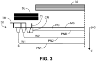
- each channel 20 contains a dedicated UV sensing device having a UV photodiode structure 30 and a dedicated UV-type filter 32.
- the photodiode structure in each channel 20 has a strong photo-response in the UV part of the spectrum (e.g., 200 - 400 nm), and has a reduced photo-response in the visible and IR parts of the spectrum.
- a customized interference filter 32 specific to a particular drug's spectral response, is provided for either band pass or band reject operation.
- the interference filter 32 used for a particular channel 20 corresponds to the spectral response of the molecule to be sensed by that channel. Incorporating the respective interference filter 32 for each channel 20 facilitates the module's ability to discern the type of drug or other chemical substance present in the sample 14.
- the photodiode 30 in each particular drug detection channel 20 integrates the sensed UV radiation over time for the various wavelengths within the band as defined by the filter 32 for that channel.
- the expected spectral response of each chemical substance can be convoluted with the spectral responsivity of the photodiode's silicon so as to compensate for the spectral responsivity reduction of silicon at 270 nm.
- the interference filter 32 for each respective channel 20 can be configured to pass more light for those wavelengths where the UV photodiode 30 is not as sensitive, and to pass less light for those wavelengths where the UV photodiode 30 is more sensitive. In this way, the interference filter 32 for each channel 20 can be customized to reflect the inherent sensitivity versus wavelength of the UV filter.
- the convoluted curve thus represents the transmission definition of the interference filter dedicated to the specific chemical substance that the particular channel 20 is designed to detect.
- the sensor module 10 includes an analog-to-digital converter (ADC) 34 to measure the photocurrent generated by the photodiode 30 in each channel 20, 24, 26.
- ADC analog-to-digital converter
- the output responses then are transmitted to signal processing circuitry 36 for signal treatment and data analysis so as to identify whether any of the predetermined chemical substances are present in the sample 14, as well as the quantity of each chemical substance.
- the signal processing circuitry 36 is operable to identify the chemical substance(s) in the sample 14 based on an analysis of the output signals from the channels 20. As indicated by FIG.
- the sensor 18 is operable to integrate signals in multiple UV channels 20 in parallel (i.e., simultaneously) and to perform signal processing to discern responsivities that match or align with a particular spectral signature of a drug or other chemical substance.
- the integrated signal from each channel is provided to a comparison block 40 (see FIG. 4 ) which is operable to compare the output signal from each channel 20 to a respective predetermined value stored in memory 35 (see FIG. 2 ).
- the comparison block 40 can be integrated into the signal processing circuitry 36. Ratio-metric cross analysis of multiple drug substances within a single integrated system allows for quick analysis and detection by implementing relative comparisons of each channel's output responsivity.
- Signals generated by the UV clear channel 24 and the UV block channel 26 can serve as reference signals.
- a signal from the UV block channel 26 can be processed and used by the signal processing circuitry 36 to normalize the signals obtained from the UV channels 20.
- a signal from the UV clear channel 24 can be processed and used by the signal processing circuitry 36 to improve signal/noise ratio.
- Signals from the UV clear and UV block channels 24, 26 also can be used to improve the overall signal acquisition process by detecting and accounting for background radiation.
- the senor 18 has two channels for each chemical substance of interest.
- a first one of channels is configured to sense the response of the sample 14 based on its response to UV illumination as described above; the second channel is configured to sense the fluorescence effect of the sample 14.
- the signal processing circuitry 36 also is operable to analyze outputs from the channels 20 based on the fluorescence effect of the sample 14. By analyzing signals output by the channels 20 when the sample 14 is illuminated 14 directly with UV radiation, as well as signals output by the channels 20 resulting from the fluorescent effect, greater accuracy can be achieved in identifying the chemical substance of the sample 14.
- the sample 14 may emit radiation in the UV range even in the absence of illuminating the sample with UV radiation. In such instances, it may be unnecessary to illuminate the sample 14 with UV radiation from the tunable monochromatic UV light source.
- the module 10 includes an on-die temperature sensor coupled to a temperature controller 38 to provide temperature-dependent leakage current compensation of the UV photodiode 30 in each channel 20. Incorporating the temperature controller 38 can aid in temperature-drift offset correction from the front-end ADC 34 resulting from photodiode leakage and general transistor leakage from the analog front-end.
- the temperature controller 38 also can be incorporated as part of the signal processing circuitry 36.
- the signal processing circuitry 36 can be implemented, for example, as an integrated circuit. In some cases, the processing circuitry 36 may include software and/or firmware. An output of the signal processing circuitry 36 can be coupled, for example, to a monitor or other display unit to indicate whether there is a match between the chemical substance of the sample 14 and the spectral signature associated with any one of the channels 20 and, if so, to identify the chemical substance detected, as well as the quantity detected.
- a photodiode structure 30 suitable for use in the channels 20 of the sensor 18 includes a superposition of two wells, in particular two ion-implanted wells, with opposite types of electrical conductivity within a semiconductor substrate.
- the semiconductor substrate has a first type of electrical conductivity, whereas a first well has a second type, and a second well has the first type.
- a photon capturing layer having the second type of electrical conductivity is formed at a main surface of the semiconductor substrate.
- a p-n junction formed between the photon capturing layer and the second well is usable for detecting incident UV radiation.
- the photodiode structure 30 can be implemented, for example, in a semiconductor wafer or a semiconductor die and/or can be part of an integrated circuit.
- the UV photodiode structure 30 includes a semiconductor substrate S including a semiconductor material, for example silicon, and having a first type of electrical conductivity, for example p-type conductivity.
- the photodiode structure further includes a first well W1 arranged within the semiconductor substrate S and having a second type of electrical conductivity opposite to the first type, the second type being, for example, n-type conductivity.
- the photodiode structure 30 further includes a second well W2 arranged, for example, within the first well W1 and having the first type of electrical conductivity.
- a first p-n junction PN1 is formed by a boundary between the semiconductor substrate S and the first well W1
- a second p-n junction PN2 is formed by a boundary between the first well W1 and the second well W2.
- a photodiode structure is predominantly sensitive to UV radiation, and the sensitivity to visible light or infrared radiation is reduced.
- a doping concentration, in particular a carrier concentration, of the first well W1 is greater than a doping concentration, in particular a carrier concentration, of the second well W2. Therefore, a photon capturing layer PC having the second type of electrical conductivity is formed at the main surface MS, in particular in the surface region. Thus, a detection p-n junction PND is formed by a boundary between the second well W2 and the photon capturing layer PC.
- a part of the second well W2 not corresponding to the photon capturing layer PC is denoted as the second well W2
- a part of the first well W1 corresponding neither to the second well W2 nor to the photon capturing layer PC is denoted as the first well W1.
- the photodiode structure 30 includes a contact region CR having the second type of electrical conductivity within the semiconductor substrate for contacting the photon capturing layer PC.
- the photodiode structure 30 further includes a first sense terminal T1 connected to the photon capturing layer PC, for example, via the contact region CR.
- the photodiode structure 30 can include a reference terminal TR connected to the semiconductor substrate S, the first well W1 and second well W2.
- the reference terminal TR is connected to the semiconductor substrate S and the first well W1
- the photodiode device includes a further reference terminal connected to the second well W2.
- a photodiode structure 30 of the sensor device of FIG. 3 is formed by the first and the second wells W1, W2 and the resulting photon capturing layer PC.
- the detection p-n junction PND can be used to detect UV radiation.
- a photocurrent generated within the depletion region of the detection p-n junction PND can, for example, be read out or measured via the first sense terminal T1.
- UV radiation sensing device in each channel of the sensor 18.
- FIG. 5 illustrates a method not according to the invention and provided for illustration purposes only.
- the method includes placing a sample in an integrated sensor module operable for detection of chemical substances (100), and emitting UV radiation from a UV radiation source onto the sample (102).
- the method further includes receiving UV radiation from the sample in each of a plurality of spectrally sensitive UV channels (104), each of the UV channels including a respective sensing device and a respective UV interference filter disposed over a UV radiation sensitive portion of the respective sensing device.
- the respective UV interference filter for each particular one of the channels has transmission characteristics that are spectrally responsive to a spectral signature of a respective chemical substance.
- the method includes integrating signals in each of the UV channels in parallel.
- the method includes providing a respective integrated signal from each of the UV channels to a signal processor (106), and determining, based at least in part on the respective integrated signals from the UV channels, whether a respective responsivity matches or aligns with the spectral signature of the chemical substance associated with any particular one of the UV channels (108). Determining whether a respective responsivity matches or aligns with the spectral signature of the chemical substance associated with any particular one of the UV channels can include, for example, comparing the respective integrated signals from the UV channels to respective predetermined values. In some instances, the method includes identifying a composition of the sample based at least in part on the comparison (110).
Landscapes
- Physics & Mathematics (AREA)
- Spectroscopy & Molecular Physics (AREA)
- General Physics & Mathematics (AREA)
- Biochemistry (AREA)
- Chemical & Material Sciences (AREA)
- Analytical Chemistry (AREA)
- Life Sciences & Earth Sciences (AREA)
- General Health & Medical Sciences (AREA)
- Health & Medical Sciences (AREA)
- Immunology (AREA)
- Pathology (AREA)
- Investigating, Analyzing Materials By Fluorescence Or Luminescence (AREA)
- Investigating Or Analysing Materials By Optical Means (AREA)
Description
- This disclosure relates to integrated sensor modules for the detection of chemical substances.
- Various techniques have been proposed for testing chemical substances in laboratory and point-of-care settings. Such tests can be used, for example, for forensic testing of samples to detect the presence of illicit substances (e.g., drugs). The tests can be used, for example, to assist police of other governmental enforcement agencies, as well as by hospitals, harm reduction agencies and patient clinics that care for patients or persons in drug rehabilitation facilities.
- The following are examples of techniques that can be used to test for chemical substances: mass spectrometry; infrared spectrometry, Raman spectrometry, x-ray spectrometry, thin-layer chromatography, ultraviolet spectroscopy, spot/color tests, microcrystalline tests, immunoassays and urine dipstick tests. The techniques differ in their ability to discriminate among different substances, in the range of substances that can be detected and discriminated, in their ability to determine the quantity of the particular substance detected, in the relative costs of the tests, and in the ease of using the tests.
US2007/138401 A1 discloses an integrated sensor module for detection and discrimination between chemical substances, a UV radiation source operable to emit UV radiation onto a sample and a sensor including a plurality of spectrally sensitive UV channels disposed so as to receive UV radiation from the sample in each of the UV channels including a respective sensing device and a respective UV interference filter disposed over a UV radiation sensitive portion of the respective sensing device. - In general, it is desirable to provide a low cost integrated sensor that can detect and discriminate among a wide range of chemical substances. Preferably, the sensor should provide increased accuracy and be relatively simple to use.
- This disclosure describes integrated sensor modules for the detection of chemical substances.
- For example, in one aspect, the disclosure describes an integrated sensor module as set out in the appended set of claims.
- Some implementations include one or more of the following features. For example, in some instances, the sensor is operable to integrate signals in each of the plurality of UV channels in parallel.
- In accordance with another aspect, a method as set out in the appended set of claims is provided.
- In some implementations, the method includes integrating signals in each of the UV channels in parallel.
- Other aspects, features and advantages will be readily apparent from the following detailed description, the accompanying drawings, and the claims.
-
-
FIG. 1 illustrates an example of a chemical substance detection sensor module. -
FIG. 2 is a block diagram illustrating various functional components of the sensor module. -
FIG. 3 is a schematic illustrating an example of a UV sensing device. -
FIG. 4 is a schematic illustrating signal processing of signals from the sensor module channels. -
FIG. 5 is a flow chart illustrating a method in accordance with the present disclosure. - The present disclosure describes an integrated sensor module operable to detect and discriminate among different chemical substances, such as particulate matter (e.g., molecules of illegal drugs) present in a sample. The sensor module is operable, in some instances, for real-time measurements in which a radiation source emits ultraviolet (UV) radiation toward the sample, and UV radiation reflected by the sample is detected and integrated in an array of spectrally sensitive UV channels. The array includes multiple UV channels each of which is spectrally sensitive, and isolated, to a particular chemical substance (e.g., a drug).
- As illustrated in the example of
FIG. 1 , a chemical substancedetection sensor module 10 includes anoptical source 12 operable to emit UV radiation toward a sample 14 (e.g., a solid, liquid or gas). Theradiation source 12 can include, for example, a tunable monochromatic UV light source operable to emit radiation in the range of about 200 - 400 nm. Theradiation source 12 also includes a second switchable broad band radiation source operable to emit longer wavelengths (e.g., up to 900 nm) that is used to test the fluorescence effect of the sample 14 (i.e., to detect a peak wavelength reflected by the sample). Anoptical system 16, including one or more lenses or other optical elements, can be provided in the path of the radiation emitted by thesource 12 so as to focus the emitted radiation onto thesample 14. At least some of the radiation reflected by the sample is sensed by asensor 18 that includes an array of radiationsensitive channels 20. - Each
channel 20 incorporates a respective UV sensitive photodiode as well as a UV interference filter having transmission characteristics that are spectrally responsive to the spectral signature of a respective drug or other chemical substance. Thus, for example, if thesensor 18 includes an array of fiftychannels 20, themodule 10 can be operable to detect up to fifty different chemical substances, each of which has a spectral signature that differs from the spectral signature of the chemical substances detectable by theother channels 20. - A
radiation shield 22 can be disposed between theradiation source 12 and thesensor 18 so as to prevent radiation emitted by thesource 12 from directly impinging on thechannels 20 of thesensor 18. Preferably, theshield 12 is composed of a material that is non-reflective and non-transmissive for UV radiation. Themodule 10 can be contained in a dark,non-reflective chamber 28 that isolates thesensor 18 from external parasitic radiation. - As shown in
FIG. 2 , in addition to the UVsensitive channels 20, thesensor 18 can include additional channels to help discriminate and measure the UV in-band and out-band radiation. For example, thesensor 18 can include aclear UV channel 24 having a band pass filter that selectively passes, for example, UV radiation in a predetermined range (e.g., 200 - 400 nm). Thus, the UVclear channel 24 is operable to measure the overall UV response of thesample 14 within the predetermined UV range. Further, thesensor 18 can include aUV block channel 26, which passes non-UV radiation (e.g., visible light and infrared (IR) radiation), but blocks UV radiation. TheUV block channel 26 allows themodule 10 to measure the out of band radiation seen by thesample 14. - As illustrated in the example of
FIG. 3 , eachchannel 20 contains a dedicated UV sensing device having a UV photodiode structure 30 and a dedicated UV-type filter 32. Preferably, the photodiode structure in eachchannel 20 has a strong photo-response in the UV part of the spectrum (e.g., 200 - 400 nm), and has a reduced photo-response in the visible and IR parts of the spectrum. - Various chemical substances (e.g., drugs) inherently have unique spectral responses to the
UV light source 12. A customizedinterference filter 32, specific to a particular drug's spectral response, is provided for either band pass or band reject operation. Theinterference filter 32 used for aparticular channel 20 corresponds to the spectral response of the molecule to be sensed by that channel. Incorporating therespective interference filter 32 for eachchannel 20 facilitates the module's ability to discern the type of drug or other chemical substance present in thesample 14. The photodiode 30 in each particulardrug detection channel 20 integrates the sensed UV radiation over time for the various wavelengths within the band as defined by thefilter 32 for that channel. - To improve sensitivity, the expected spectral response of each chemical substance can be convoluted with the spectral responsivity of the photodiode's silicon so as to compensate for the spectral responsivity reduction of silicon at 270 nm. Thus, the
interference filter 32 for eachrespective channel 20 can be configured to pass more light for those wavelengths where the UV photodiode 30 is not as sensitive, and to pass less light for those wavelengths where the UV photodiode 30 is more sensitive. In this way, theinterference filter 32 for eachchannel 20 can be customized to reflect the inherent sensitivity versus wavelength of the UV filter. The convoluted curve thus represents the transmission definition of the interference filter dedicated to the specific chemical substance that theparticular channel 20 is designed to detect. - As further illustrated in
FIG. 2 , thesensor module 10 includes an analog-to-digital converter (ADC) 34 to measure the photocurrent generated by the photodiode 30 in eachchannel signal processing circuitry 36 for signal treatment and data analysis so as to identify whether any of the predetermined chemical substances are present in thesample 14, as well as the quantity of each chemical substance. Thesignal processing circuitry 36 is operable to identify the chemical substance(s) in thesample 14 based on an analysis of the output signals from thechannels 20. As indicated byFIG. 4 , thesensor 18 is operable to integrate signals inmultiple UV channels 20 in parallel (i.e., simultaneously) and to perform signal processing to discern responsivities that match or align with a particular spectral signature of a drug or other chemical substance. The integrated signal from each channel is provided to a comparison block 40 (seeFIG. 4 ) which is operable to compare the output signal from eachchannel 20 to a respective predetermined value stored in memory 35 (seeFIG. 2 ). Thecomparison block 40 can be integrated into thesignal processing circuitry 36. Ratio-metric cross analysis of multiple drug substances within a single integrated system allows for quick analysis and detection by implementing relative comparisons of each channel's output responsivity. - Signals generated by the UV
clear channel 24 and theUV block channel 26 can serve as reference signals. For example, a signal from theUV block channel 26 can be processed and used by thesignal processing circuitry 36 to normalize the signals obtained from theUV channels 20. Likewise, a signal from the UVclear channel 24 can be processed and used by thesignal processing circuitry 36 to improve signal/noise ratio. Signals from the UV clear andUV block channels - In some instances, the
sensor 18 has two channels for each chemical substance of interest. A first one of channels is configured to sense the response of thesample 14 based on its response to UV illumination as described above; the second channel is configured to sense the fluorescence effect of thesample 14. In such cases, thesignal processing circuitry 36 also is operable to analyze outputs from thechannels 20 based on the fluorescence effect of thesample 14. By analyzing signals output by thechannels 20 when thesample 14 is illuminated 14 directly with UV radiation, as well as signals output by thechannels 20 resulting from the fluorescent effect, greater accuracy can be achieved in identifying the chemical substance of thesample 14. In some cases, thesample 14 may emit radiation in the UV range even in the absence of illuminating the sample with UV radiation. In such instances, it may be unnecessary to illuminate thesample 14 with UV radiation from the tunable monochromatic UV light source. - In some implementations, the
module 10 includes an on-die temperature sensor coupled to atemperature controller 38 to provide temperature-dependent leakage current compensation of the UV photodiode 30 in eachchannel 20. Incorporating thetemperature controller 38 can aid in temperature-drift offset correction from the front-end ADC 34 resulting from photodiode leakage and general transistor leakage from the analog front-end. Thetemperature controller 38 also can be incorporated as part of thesignal processing circuitry 36. - The
signal processing circuitry 36 can be implemented, for example, as an integrated circuit. In some cases, theprocessing circuitry 36 may include software and/or firmware. An output of thesignal processing circuitry 36 can be coupled, for example, to a monitor or other display unit to indicate whether there is a match between the chemical substance of thesample 14 and the spectral signature associated with any one of thechannels 20 and, if so, to identify the chemical substance detected, as well as the quantity detected. - In some implementations, a photodiode structure 30 suitable for use in the
channels 20 of thesensor 18 includes a superposition of two wells, in particular two ion-implanted wells, with opposite types of electrical conductivity within a semiconductor substrate. The semiconductor substrate has a first type of electrical conductivity, whereas a first well has a second type, and a second well has the first type. By adjusting doping concentrations or profiles of the wells, a photon capturing layer having the second type of electrical conductivity is formed at a main surface of the semiconductor substrate. A p-n junction formed between the photon capturing layer and the second well is usable for detecting incident UV radiation. The photodiode structure 30 can be implemented, for example, in a semiconductor wafer or a semiconductor die and/or can be part of an integrated circuit. - As shown in the example of
FIG. 3 , the UV photodiode structure 30 includes a semiconductor substrate S including a semiconductor material, for example silicon, and having a first type of electrical conductivity, for example p-type conductivity. The photodiode structure further includes a first well W1 arranged within the semiconductor substrate S and having a second type of electrical conductivity opposite to the first type, the second type being, for example, n-type conductivity. The photodiode structure 30 further includes a second well W2 arranged, for example, within the first well W1 and having the first type of electrical conductivity. Consequently, a first p-n junction PN1 is formed by a boundary between the semiconductor substrate S and the first well W1, and a second p-n junction PN2 is formed by a boundary between the first well W1 and the second well W2. Advantageously, such a photodiode structure is predominantly sensitive to UV radiation, and the sensitivity to visible light or infrared radiation is reduced. - Within a surface region at a main surface MS of the semiconductor substrate S, a doping concentration, in particular a carrier concentration, of the first well W1 is greater than a doping concentration, in particular a carrier concentration, of the second well W2. Therefore, a photon capturing layer PC having the second type of electrical conductivity is formed at the main surface MS, in particular in the surface region. Thus, a detection p-n junction PND is formed by a boundary between the second well W2 and the photon capturing layer PC. In this example, a part of the second well W2 not corresponding to the photon capturing layer PC is denoted as the second well W2, and a part of the first well W1 corresponding neither to the second well W2 nor to the photon capturing layer PC is denoted as the first well W1.
- In the example of
FIG. 3 , the photodiode structure 30 includes a contact region CR having the second type of electrical conductivity within the semiconductor substrate for contacting the photon capturing layer PC. The photodiode structure 30 further includes a first sense terminal T1 connected to the photon capturing layer PC, for example, via the contact region CR. Furthermore, the photodiode structure 30 can include a reference terminal TR connected to the semiconductor substrate S, the first well W1 and second well W2. In some implementations, the reference terminal TR is connected to the semiconductor substrate S and the first well W1, and the photodiode device includes a further reference terminal connected to the second well W2. - A photodiode structure 30 of the sensor device of
FIG. 3 is formed by the first and the second wells W1, W2 and the resulting photon capturing layer PC. In particular, the detection p-n junction PND can be used to detect UV radiation. A photocurrent generated within the depletion region of the detection p-n junction PND can, for example, be read out or measured via the first sense terminal T1. - In some implementations, other structures can be used for the UV radiation sensing device in each channel of the
sensor 18. -
FIG. 5 illustrates a method not according to the invention and provided for illustration purposes only. The method includes placing a sample in an integrated sensor module operable for detection of chemical substances (100), and emitting UV radiation from a UV radiation source onto the sample (102). The method further includes receiving UV radiation from the sample in each of a plurality of spectrally sensitive UV channels (104), each of the UV channels including a respective sensing device and a respective UV interference filter disposed over a UV radiation sensitive portion of the respective sensing device. The respective UV interference filter for each particular one of the channels has transmission characteristics that are spectrally responsive to a spectral signature of a respective chemical substance. In some instances, the method includes integrating signals in each of the UV channels in parallel. The method includes providing a respective integrated signal from each of the UV channels to a signal processor (106), and determining, based at least in part on the respective integrated signals from the UV channels, whether a respective responsivity matches or aligns with the spectral signature of the chemical substance associated with any particular one of the UV channels (108). Determining whether a respective responsivity matches or aligns with the spectral signature of the chemical substance associated with any particular one of the UV channels can include, for example, comparing the respective integrated signals from the UV channels to respective predetermined values. In some instances, the method includes identifying a composition of the sample based at least in part on the comparison (110). - Various modifications can be made within the scope of the appended claims.
Claims (12)
- An integrated sensor module for detection and discrimination between chemical substances, the sensor module comprising:a UV radiation source (12) operable to emit UV radiation onto a sample (14); anda sensor (18) including a plurality of spectrally sensitive UV channels (20) disposed so as to receive UV radiation from the sample (14), each of the UV channels (20) including a respective sensing device and a respective UV interference filter (32) disposed over a UV radiation sensitive portion of the respective sensing device, the respective UV interference filter (32) for each particular one of the channels (20) having transmission characteristics that are spectrally responsive to a respectively different spectral signature of a respective chemical substance;a separate broad band radiation source operable to emit broad band radiation at longer wavelengths than the UV radiation source, outside the UV, onto the sample (14), wherein at least some channels (20) in the sensor (18) are operable to detect radiation based on a fluorescence effect of the sample (14) in response to the broad band radiation and to provide output signals to a signal processor.
- The integrated sensor module of claim 1 wherein the sensor (18) is operable to integrate signals in each of the plurality of UV channels (20) in parallel, the sensor module further including the signal processor operable to perform signal processing of signals from the UV channels (20) to determine whether a respective responsivity matches or aligns with the spectral signature of the chemical substance associated with any particular one of the UV channels (20).
- The integrated sensor module of claim 2 wherein the sensor (18) is coupled to the signal processor such that the integrated signals from the UV channels (20) can be provided to the signal processor for comparison to respective predetermined values stored in memory (35).
- The integrated sensor module of any one of the previous claims wherein the sensor (18) further includes a UV clear channel (24) operable to measure an overall UV response of the sample (14) within a predetermined UV range.
- The integrated sensor module of any one of the previous claims wherein the sensor (18) further includes a UV block channel (26) operable to pass non-UV radiation and to block UV radiation.
- The integrated sensor module of any one of the previous claims wherein the sensing device of each UV channel includes a photodiode structure (30).
- The integrated sensor module of claim 6 wherein the photodiode structure (30) includes a superposition of two ion-implanted wells having opposite types of electrical conductivity; optionally wherein the photodiode structure (30) includes a photon capturing layer having the second type of electrical conductivity, wherein a p-n junction formed between the photon capturing layer and the second well is operable to detect incident UV radiation.
- The integrated sensor module of any one of the previous claims further including a display coupled to an output of the signal processor, the display being operable to provide a visual indication of a composition of the sample (14) based on whether the respective responsivity matches or aligns with the spectral signature of the chemical substance associated with any particular one of the UV channels (20).
- A method comprising:placing a sample (14) in an integrated sensor module (100) operable for detection and discrimination between chemical substances;emitting UV radiation from a UV radiation source (12) onto the sample (14);emitting broad band radiation at longer wavelengths than the UV radiation source, outside the UV, from a separate broad band radiation source onto the sample (14);receiving UV radiation from the sample (14) in each of a plurality of spectrally sensitive UV channels (20), each of the UV channels (20) including a respective sensing device and a respective UV interference filter (32) disposed over a UV radiation sensitive portion of the respective sensing device, the respective UV interference filter (32) for each particular one of the channels (20) having transmission characteristics that are spectrally responsive to a respectively different spectral signature of a respective chemical substanceproviding a respective integrated signal from each of the UV channels (20) to a signal processor (106);detecting radiation based on a fluorescence effect of the sample (14) in response to the broad band radiation using at least some channels (20) in the sensor (18) and providing output signals to the signal processor (106);determining, based at least in part on the respective integrated signals from the UV channels, whether a respective response matches or aligns with the spectral signature of the chemical substance associated with any particular one of the UV channels; andwherein the method includes determining, based at least in part on the respective integrated signals from the UV channels (20), whether the respective response matches or aligns with the spectral signature of the chemical substance associated with any particular one of the UV channels (20).
- The method of claim 9 including integrating signals in each of the plurality of UV channels (20) in parallel.
- The method of claim 9 or claim 10 wherein said determining includes comparing the respective integrated signals from the UV channels (20) to respective predetermined values.
- The method of claim 11 including identifying a composition of the sample (14) based at least in part on said comparing.
Applications Claiming Priority (2)
| Application Number | Priority Date | Filing Date | Title |
|---|---|---|---|
| US201862684887P | 2018-06-14 | 2018-06-14 | |
| PCT/EP2019/065660 WO2019238915A1 (en) | 2018-06-14 | 2019-06-14 | Integrated sensor modules for detection of chemical substances |
Publications (2)
| Publication Number | Publication Date |
|---|---|
| EP3807606A1 EP3807606A1 (en) | 2021-04-21 |
| EP3807606B1 true EP3807606B1 (en) | 2024-03-06 |
Family
ID=66999805
Family Applications (1)
| Application Number | Title | Priority Date | Filing Date |
|---|---|---|---|
| EP19732301.7A Active EP3807606B1 (en) | 2018-06-14 | 2019-06-14 | Integrated sensor modules for detection of chemical substances |
Country Status (4)
| Country | Link |
|---|---|
| US (1) | US20210255097A1 (en) |
| EP (1) | EP3807606B1 (en) |
| CN (1) | CN112567216A (en) |
| WO (1) | WO2019238915A1 (en) |
Family Cites Families (24)
| Publication number | Priority date | Publication date | Assignee | Title |
|---|---|---|---|---|
| SU1000778A1 (en) * | 1981-10-09 | 1983-02-28 | Ордена Трудового Красного Знамени Институт Физики Ан Бсср | Spectral instrument for rapid measuring of monochromatic radiation wave length |
| CH684971A5 (en) * | 1989-03-16 | 1995-02-15 | Landis & Gyr Tech Innovat | Ultraviolet light sensor. |
| US5936250A (en) * | 1997-07-24 | 1999-08-10 | General Monitors, Incorporated | Ultraviolet toxic gas point detector |
| JP4031824B2 (en) * | 2001-05-22 | 2008-01-09 | ゼロックス コーポレイション | Color correction system for color printing and spectrophotometer |
| CA2460071A1 (en) * | 2001-09-19 | 2003-03-27 | Joule Microsystems Canada Inc. | A spectrometer incorporating signal matched filtering |
| EP1495292A4 (en) * | 2001-12-21 | 2012-05-09 | Malvern Instr Inc | Spectrometric process monitoring |
| US8395769B2 (en) * | 2002-01-10 | 2013-03-12 | Chemimage Corporation | Method for analysis of pathogenic microorganisms using raman spectroscopic techniques |
| EP1601956A2 (en) * | 2003-02-24 | 2005-12-07 | CDEX, Inc. | System and methods for detection and identification of chemical substances |
| KR100563025B1 (en) * | 2003-09-08 | 2006-03-22 | 강성준 | Apparatus and method for acquiring spectrum response of the Optical-Sensor |
| DE102004035494A1 (en) * | 2004-07-22 | 2006-02-09 | Giesecke & Devrient Gmbh | Device and method for checking value documents |
| WO2007044593A2 (en) * | 2005-10-07 | 2007-04-19 | Chemimage Corporation | System and method for a chemical imaging threat assessor with a probe |
| US7372039B2 (en) * | 2005-12-20 | 2008-05-13 | Ecolab Inc. | Near UV absorption spectrometer and method for using the same |
| JP2007232402A (en) * | 2006-02-27 | 2007-09-13 | Denso Corp | Optical gas detector |
| CN101378067B (en) * | 2007-08-31 | 2010-09-29 | 邵剑心 | Characteristic spectrum identification chip, manufacturing method thereof and detection device using the chip |
| US8124936B1 (en) * | 2007-12-13 | 2012-02-28 | The United States Of America As Represented By The Secretary Of The Army | Stand-off chemical detector |
| US8645082B2 (en) * | 2010-09-13 | 2014-02-04 | Mks Instruments, Inc. | Monitoring, detecting and quantifying chemical compounds in a sample |
| CN103983356B (en) * | 2014-05-30 | 2016-03-02 | 苏州大学 | A kind of spectrum calibration method |
| EP3191811A4 (en) * | 2014-09-11 | 2018-04-25 | Heptagon Micro Optics Pte. Ltd. | Determining spectral emission characteristics of incident radiation |
| US9534955B2 (en) * | 2014-11-06 | 2017-01-03 | Maxim Integrated Products, Inc. | Multi-channel UV detection for improved solar spectrum and UV index estimation |
| CN104677870A (en) * | 2015-02-06 | 2015-06-03 | 余家昌 | Superminiaturization multi-channel real-time fluorescent spectrum detector |
| EP3229278B1 (en) * | 2016-04-07 | 2023-08-09 | ams AG | Sensor device and method for manufacturing a sensor device |
| EP3404382A1 (en) * | 2017-05-16 | 2018-11-21 | ams AG | Optical sensor and method for detecting electromagnetic radiation |
| CN111380816A (en) * | 2018-12-27 | 2020-07-07 | 光谱引擎股份公司 | Method and system for analyzing chemical composition of target |
| KR20230039659A (en) * | 2020-07-24 | 2023-03-21 | 트리나미엑스 게엠베하 | Spectrometer device and method for measuring optical radiation |
-
2019
- 2019-06-14 CN CN201980053457.XA patent/CN112567216A/en active Pending
- 2019-06-14 EP EP19732301.7A patent/EP3807606B1/en active Active
- 2019-06-14 WO PCT/EP2019/065660 patent/WO2019238915A1/en active Application Filing
- 2019-06-14 US US17/252,184 patent/US20210255097A1/en active Pending
Also Published As
| Publication number | Publication date |
|---|---|
| US20210255097A1 (en) | 2021-08-19 |
| WO2019238915A1 (en) | 2019-12-19 |
| EP3807606A1 (en) | 2021-04-21 |
| CN112567216A (en) | 2021-03-26 |
Similar Documents
| Publication | Publication Date | Title |
|---|---|---|
| US20020161289A1 (en) | Detector array for optical spectrographs | |
| JP5575355B2 (en) | UV protection effect evaluation device | |
| US7179654B2 (en) | Biochemical assay with programmable array detection | |
| US6836332B2 (en) | Instrument and method for testing fluid characteristics | |
| Obahiagbon et al. | A compact, low-cost, quantitative and multiplexed fluorescence detection platform for point-of-care applications | |
| de Carvalho Oliveira et al. | RGB color sensor for colorimetric determinations: Evaluation and quantitative analysis of colored liquid samples | |
| US8203635B2 (en) | Image sensor with a spectrum sensor | |
| Soares et al. | Multiplexed microfluidic fluorescence immunoassay with photodiode array signal acquisition for sub-minute and point-of-need detection of mycotoxins | |
| Hussain et al. | Design of a smartphone platform compact optical system operational both in visible and near infrared spectral regime | |
| RU2009105488A (en) | METHOD AND DEVICE FOR DETERMINING INTENSIVE AND PEAK LENGTHS OF LIGHT WAVES | |
| US11112362B2 (en) | Portable in-vitro diagnostic detector and apparatus | |
| WO2017019762A1 (en) | Image based photometry | |
| US20220022784A1 (en) | Non-invasive Glucose Sensor | |
| Sander et al. | Low-noise CMOS fluorescence sensor | |
| US7532128B2 (en) | Position sensitive indicator detection | |
| EP3807606B1 (en) | Integrated sensor modules for detection of chemical substances | |
| US20220357204A1 (en) | Integrated sensor modules for detection of chemical substances | |
| EP2171432B1 (en) | A detection apparatus and method | |
| KR101383338B1 (en) | Reflectivity measuring device for color information with LED and Phototransistor | |
| CN108387531B (en) | Spectrum detection device and method | |
| Hofmann et al. | An integrated CMOS photodiode array for highly sensitive photometric diagnostics | |
| Fakki et al. | Optical mouse as pH analyzer | |
| Margalith et al. | Near infrared spectral imaging of explosives using a tunable laser source | |
| CN103472040A (en) | Fluorescence detection method | |
| WO2020030615A1 (en) | Devices and method for measuring an analyte concentration in a sample of bodily fluid |
Legal Events
| Date | Code | Title | Description |
|---|---|---|---|
| STAA | Information on the status of an ep patent application or granted ep patent |
Free format text: STATUS: UNKNOWN |
|
| STAA | Information on the status of an ep patent application or granted ep patent |
Free format text: STATUS: THE INTERNATIONAL PUBLICATION HAS BEEN MADE |
|
| STAA | Information on the status of an ep patent application or granted ep patent |
Free format text: STATUS: THE INTERNATIONAL PUBLICATION HAS BEEN MADE |
|
| PUAI | Public reference made under article 153(3) epc to a published international application that has entered the european phase |
Free format text: ORIGINAL CODE: 0009012 |
|
| STAA | Information on the status of an ep patent application or granted ep patent |
Free format text: STATUS: REQUEST FOR EXAMINATION WAS MADE |
|
| 17P | Request for examination filed |
Effective date: 20210113 |
|
| AK | Designated contracting states |
Kind code of ref document: A1 Designated state(s): AL AT BE BG CH CY CZ DE DK EE ES FI FR GB GR HR HU IE IS IT LI LT LU LV MC MK MT NL NO PL PT RO RS SE SI SK SM TR |
|
| AX | Request for extension of the european patent |
Extension state: BA ME |
|
| DAV | Request for validation of the european patent (deleted) | ||
| DAX | Request for extension of the european patent (deleted) | ||
| STAA | Information on the status of an ep patent application or granted ep patent |
Free format text: STATUS: EXAMINATION IS IN PROGRESS |
|
| 17Q | First examination report despatched |
Effective date: 20220908 |
|
| GRAP | Despatch of communication of intention to grant a patent |
Free format text: ORIGINAL CODE: EPIDOSNIGR1 |
|
| STAA | Information on the status of an ep patent application or granted ep patent |
Free format text: STATUS: GRANT OF PATENT IS INTENDED |
|
| P01 | Opt-out of the competence of the unified patent court (upc) registered |
Effective date: 20230613 |
|
| GRAJ | Information related to disapproval of communication of intention to grant by the applicant or resumption of examination proceedings by the epo deleted |
Free format text: ORIGINAL CODE: EPIDOSDIGR1 |
|
| STAA | Information on the status of an ep patent application or granted ep patent |
Free format text: STATUS: EXAMINATION IS IN PROGRESS |
|
| INTG | Intention to grant announced |
Effective date: 20230704 |
|
| INTC | Intention to grant announced (deleted) | ||
| GRAP | Despatch of communication of intention to grant a patent |
Free format text: ORIGINAL CODE: EPIDOSNIGR1 |
|
| STAA | Information on the status of an ep patent application or granted ep patent |
Free format text: STATUS: GRANT OF PATENT IS INTENDED |
|
| INTG | Intention to grant announced |
Effective date: 20230925 |
|
| GRAS | Grant fee paid |
Free format text: ORIGINAL CODE: EPIDOSNIGR3 |
|
| GRAA | (expected) grant |
Free format text: ORIGINAL CODE: 0009210 |
|
| STAA | Information on the status of an ep patent application or granted ep patent |
Free format text: STATUS: THE PATENT HAS BEEN GRANTED |
|
| AK | Designated contracting states |
Kind code of ref document: B1 Designated state(s): AL AT BE BG CH CY CZ DE DK EE ES FI FR GB GR HR HU IE IS IT LI LT LU LV MC MK MT NL NO PL PT RO RS SE SI SK SM TR |
|
| REG | Reference to a national code |
Ref country code: CH Ref legal event code: EP |
|
| REG | Reference to a national code |
Ref country code: IE Ref legal event code: FG4D |
|
| REG | Reference to a national code |
Ref country code: DE Ref legal event code: R096 Ref document number: 602019047767 Country of ref document: DE |