EP3791820B9 - High density electrode mapping catheter - Google Patents
High density electrode mapping catheter Download PDFInfo
- Publication number
- EP3791820B9 EP3791820B9 EP20203250.4A EP20203250A EP3791820B9 EP 3791820 B9 EP3791820 B9 EP 3791820B9 EP 20203250 A EP20203250 A EP 20203250A EP 3791820 B9 EP3791820 B9 EP 3791820B9
- Authority
- EP
- European Patent Office
- Prior art keywords
- understructure
- inboard
- arm
- outboard
- microelectrodes
- Prior art date
- Legal status (The legal status is an assumption and is not a legal conclusion. Google has not performed a legal analysis and makes no representation as to the accuracy of the status listed.)
- Active
Links
- 238000013507 mapping Methods 0.000 title description 81
- 239000003989 dielectric material Substances 0.000 claims description 92
- 238000000034 method Methods 0.000 claims description 78
- 239000000758 substrate Substances 0.000 claims description 34
- 230000008569 process Effects 0.000 claims description 22
- 238000007747 plating Methods 0.000 claims description 7
- 239000010410 layer Substances 0.000 description 97
- 239000000463 material Substances 0.000 description 66
- 210000001519 tissue Anatomy 0.000 description 50
- 230000007704 transition Effects 0.000 description 41
- 238000012360 testing method Methods 0.000 description 36
- 239000004020 conductor Substances 0.000 description 32
- 238000000576 coating method Methods 0.000 description 30
- 239000011248 coating agent Substances 0.000 description 28
- 238000002679 ablation Methods 0.000 description 27
- 229910000679 solder Inorganic materials 0.000 description 24
- 239000008280 blood Substances 0.000 description 23
- 210000004369 blood Anatomy 0.000 description 23
- 229920000642 polymer Polymers 0.000 description 21
- HLXZNVUGXRDIFK-UHFFFAOYSA-N nickel titanium Chemical compound [Ti].[Ti].[Ti].[Ti].[Ti].[Ti].[Ti].[Ti].[Ti].[Ti].[Ti].[Ni].[Ni].[Ni].[Ni].[Ni].[Ni].[Ni].[Ni].[Ni].[Ni].[Ni].[Ni].[Ni].[Ni] HLXZNVUGXRDIFK-UHFFFAOYSA-N 0.000 description 17
- 229910001000 nickel titanium Inorganic materials 0.000 description 17
- 230000004913 activation Effects 0.000 description 16
- 230000000747 cardiac effect Effects 0.000 description 16
- 238000012545 processing Methods 0.000 description 15
- PXHVJJICTQNCMI-UHFFFAOYSA-N Nickel Chemical compound [Ni] PXHVJJICTQNCMI-UHFFFAOYSA-N 0.000 description 12
- 239000010949 copper Substances 0.000 description 12
- 238000010586 diagram Methods 0.000 description 10
- 229910052751 metal Inorganic materials 0.000 description 10
- 239000002184 metal Substances 0.000 description 10
- 210000005003 heart tissue Anatomy 0.000 description 9
- BASFCYQUMIYNBI-UHFFFAOYSA-N platinum Chemical compound [Pt] BASFCYQUMIYNBI-UHFFFAOYSA-N 0.000 description 9
- RYGMFSIKBFXOCR-UHFFFAOYSA-N Copper Chemical compound [Cu] RYGMFSIKBFXOCR-UHFFFAOYSA-N 0.000 description 8
- 229910052802 copper Inorganic materials 0.000 description 8
- 230000000873 masking effect Effects 0.000 description 8
- 239000004593 Epoxy Substances 0.000 description 7
- 230000003247 decreasing effect Effects 0.000 description 7
- 229910052697 platinum Inorganic materials 0.000 description 6
- 102000010834 Extracellular Matrix Proteins Human genes 0.000 description 5
- 108010037362 Extracellular Matrix Proteins Proteins 0.000 description 5
- 238000013461 design Methods 0.000 description 5
- 210000002744 extracellular matrix Anatomy 0.000 description 5
- 229910052759 nickel Inorganic materials 0.000 description 5
- -1 platinum group metals Chemical class 0.000 description 5
- 229920000052 poly(p-xylylene) Polymers 0.000 description 5
- 229920002614 Polyether block amide Polymers 0.000 description 4
- 230000015572 biosynthetic process Effects 0.000 description 4
- 230000008878 coupling Effects 0.000 description 4
- 238000010168 coupling process Methods 0.000 description 4
- 238000005859 coupling reaction Methods 0.000 description 4
- 238000000151 deposition Methods 0.000 description 4
- 238000004070 electrodeposition Methods 0.000 description 4
- PCHJSUWPFVWCPO-UHFFFAOYSA-N gold Chemical compound [Au] PCHJSUWPFVWCPO-UHFFFAOYSA-N 0.000 description 4
- 229910052737 gold Inorganic materials 0.000 description 4
- 239000010931 gold Substances 0.000 description 4
- HWLDNSXPUQTBOD-UHFFFAOYSA-N platinum-iridium alloy Chemical compound [Ir].[Pt] HWLDNSXPUQTBOD-UHFFFAOYSA-N 0.000 description 4
- VYZAMTAEIAYCRO-UHFFFAOYSA-N Chromium Chemical compound [Cr] VYZAMTAEIAYCRO-UHFFFAOYSA-N 0.000 description 3
- 239000004642 Polyimide Substances 0.000 description 3
- 229910052782 aluminium Inorganic materials 0.000 description 3
- XAGFODPZIPBFFR-UHFFFAOYSA-N aluminium Chemical compound [Al] XAGFODPZIPBFFR-UHFFFAOYSA-N 0.000 description 3
- 230000009286 beneficial effect Effects 0.000 description 3
- 238000004891 communication Methods 0.000 description 3
- 238000009826 distribution Methods 0.000 description 3
- 230000003902 lesion Effects 0.000 description 3
- 230000004807 localization Effects 0.000 description 3
- 230000033001 locomotion Effects 0.000 description 3
- 229920001721 polyimide Polymers 0.000 description 3
- 239000002356 single layer Substances 0.000 description 3
- 125000006850 spacer group Chemical group 0.000 description 3
- 230000001225 therapeutic effect Effects 0.000 description 3
- JYEUMXHLPRZUAT-UHFFFAOYSA-N 1,2,3-triazine Chemical compound C1=CN=NN=C1 JYEUMXHLPRZUAT-UHFFFAOYSA-N 0.000 description 2
- XQUPVDVFXZDTLT-UHFFFAOYSA-N 1-[4-[[4-(2,5-dioxopyrrol-1-yl)phenyl]methyl]phenyl]pyrrole-2,5-dione Chemical compound O=C1C=CC(=O)N1C(C=C1)=CC=C1CC1=CC=C(N2C(C=CC2=O)=O)C=C1 XQUPVDVFXZDTLT-UHFFFAOYSA-N 0.000 description 2
- 229920000106 Liquid crystal polymer Polymers 0.000 description 2
- KDLHZDBZIXYQEI-UHFFFAOYSA-N Palladium Chemical group [Pd] KDLHZDBZIXYQEI-UHFFFAOYSA-N 0.000 description 2
- 239000000853 adhesive Substances 0.000 description 2
- 230000001070 adhesive effect Effects 0.000 description 2
- 230000001746 atrial effect Effects 0.000 description 2
- 230000004323 axial length Effects 0.000 description 2
- 238000012512 characterization method Methods 0.000 description 2
- 239000013078 crystal Substances 0.000 description 2
- 238000009713 electroplating Methods 0.000 description 2
- 239000003822 epoxy resin Substances 0.000 description 2
- 238000003384 imaging method Methods 0.000 description 2
- 238000000608 laser ablation Methods 0.000 description 2
- 230000007246 mechanism Effects 0.000 description 2
- 239000000203 mixture Substances 0.000 description 2
- 210000004165 myocardium Anatomy 0.000 description 2
- 229920003192 poly(bis maleimide) Polymers 0.000 description 2
- 229920000647 polyepoxide Polymers 0.000 description 2
- 229920001343 polytetrafluoroethylene Polymers 0.000 description 2
- 239000004810 polytetrafluoroethylene Substances 0.000 description 2
- 238000012552 review Methods 0.000 description 2
- 229910000601 superalloy Inorganic materials 0.000 description 2
- DSUFPYCILZXJFF-UHFFFAOYSA-N 4-[[4-[[4-(pentoxycarbonylamino)cyclohexyl]methyl]cyclohexyl]carbamoyloxy]butyl n-[4-[[4-(butoxycarbonylamino)cyclohexyl]methyl]cyclohexyl]carbamate Chemical compound C1CC(NC(=O)OCCCCC)CCC1CC1CCC(NC(=O)OCCCCOC(=O)NC2CCC(CC3CCC(CC3)NC(=O)OCCCC)CC2)CC1 DSUFPYCILZXJFF-UHFFFAOYSA-N 0.000 description 1
- RYECOJGRJDOGPP-UHFFFAOYSA-N Ethylurea Chemical compound CCNC(N)=O RYECOJGRJDOGPP-UHFFFAOYSA-N 0.000 description 1
- 229920001410 Microfiber Polymers 0.000 description 1
- 238000005481 NMR spectroscopy Methods 0.000 description 1
- 229910000566 Platinum-iridium alloy Inorganic materials 0.000 description 1
- 229910001260 Pt alloy Inorganic materials 0.000 description 1
- 230000004075 alteration Effects 0.000 description 1
- 238000004458 analytical method Methods 0.000 description 1
- 206010003119 arrhythmia Diseases 0.000 description 1
- 238000010009 beating Methods 0.000 description 1
- 230000008901 benefit Effects 0.000 description 1
- 238000005234 chemical deposition Methods 0.000 description 1
- 239000002131 composite material Substances 0.000 description 1
- 238000010276 construction Methods 0.000 description 1
- 230000007123 defense Effects 0.000 description 1
- 230000001419 dependent effect Effects 0.000 description 1
- 230000008021 deposition Effects 0.000 description 1
- 239000007933 dermal patch Substances 0.000 description 1
- 230000000694 effects Effects 0.000 description 1
- 239000013013 elastic material Substances 0.000 description 1
- 230000005611 electricity Effects 0.000 description 1
- 230000005518 electrochemistry Effects 0.000 description 1
- 238000005516 engineering process Methods 0.000 description 1
- 238000005530 etching Methods 0.000 description 1
- 239000011152 fibreglass Substances 0.000 description 1
- 238000001914 filtration Methods 0.000 description 1
- 238000002594 fluoroscopy Methods 0.000 description 1
- 239000011521 glass Substances 0.000 description 1
- 238000003780 insertion Methods 0.000 description 1
- 230000037431 insertion Effects 0.000 description 1
- 238000011835 investigation Methods 0.000 description 1
- 229910052741 iridium Inorganic materials 0.000 description 1
- GKOZUEZYRPOHIO-UHFFFAOYSA-N iridium atom Chemical group [Ir] GKOZUEZYRPOHIO-UHFFFAOYSA-N 0.000 description 1
- 230000001788 irregular Effects 0.000 description 1
- 238000011068 loading method Methods 0.000 description 1
- 238000004519 manufacturing process Methods 0.000 description 1
- 230000013011 mating Effects 0.000 description 1
- 238000005259 measurement Methods 0.000 description 1
- 238000001465 metallisation Methods 0.000 description 1
- 150000002739 metals Chemical class 0.000 description 1
- 239000003658 microfiber Substances 0.000 description 1
- 230000002107 myocardial effect Effects 0.000 description 1
- 229910052763 palladium Inorganic materials 0.000 description 1
- 210000003516 pericardium Anatomy 0.000 description 1
- 239000004033 plastic Substances 0.000 description 1
- 229920003023 plastic Polymers 0.000 description 1
- 239000004814 polyurethane Substances 0.000 description 1
- 229920002635 polyurethane Polymers 0.000 description 1
- 230000001012 protector Effects 0.000 description 1
- 238000007674 radiofrequency ablation Methods 0.000 description 1
- 230000009467 reduction Effects 0.000 description 1
- 238000011160 research Methods 0.000 description 1
- 239000000523 sample Substances 0.000 description 1
- 238000005476 soldering Methods 0.000 description 1
- 239000000126 substance Substances 0.000 description 1
- 230000002459 sustained effect Effects 0.000 description 1
- 230000001360 synchronised effect Effects 0.000 description 1
- 238000002560 therapeutic procedure Methods 0.000 description 1
- 238000003325 tomography Methods 0.000 description 1
- 238000002604 ultrasonography Methods 0.000 description 1
- 210000005166 vasculature Anatomy 0.000 description 1
- 230000002861 ventricular Effects 0.000 description 1
Images


Classifications
-
- A—HUMAN NECESSITIES
- A61—MEDICAL OR VETERINARY SCIENCE; HYGIENE
- A61B—DIAGNOSIS; SURGERY; IDENTIFICATION
- A61B5/00—Measuring for diagnostic purposes; Identification of persons
- A61B5/24—Detecting, measuring or recording bioelectric or biomagnetic signals of the body or parts thereof
- A61B5/25—Bioelectric electrodes therefor
- A61B5/279—Bioelectric electrodes therefor specially adapted for particular uses
- A61B5/28—Bioelectric electrodes therefor specially adapted for particular uses for electrocardiography [ECG]
- A61B5/283—Invasive
- A61B5/287—Holders for multiple electrodes, e.g. electrode catheters for electrophysiological study [EPS]
-
- A—HUMAN NECESSITIES
- A61—MEDICAL OR VETERINARY SCIENCE; HYGIENE
- A61B—DIAGNOSIS; SURGERY; IDENTIFICATION
- A61B18/00—Surgical instruments, devices or methods for transferring non-mechanical forms of energy to or from the body
- A61B18/04—Surgical instruments, devices or methods for transferring non-mechanical forms of energy to or from the body by heating
- A61B18/12—Surgical instruments, devices or methods for transferring non-mechanical forms of energy to or from the body by heating by passing a current through the tissue to be heated, e.g. high-frequency current
- A61B18/14—Probes or electrodes therefor
- A61B18/1492—Probes or electrodes therefor having a flexible, catheter-like structure, e.g. for heart ablation
-
- A—HUMAN NECESSITIES
- A61—MEDICAL OR VETERINARY SCIENCE; HYGIENE
- A61B—DIAGNOSIS; SURGERY; IDENTIFICATION
- A61B5/00—Measuring for diagnostic purposes; Identification of persons
- A61B5/24—Detecting, measuring or recording bioelectric or biomagnetic signals of the body or parts thereof
- A61B5/25—Bioelectric electrodes therefor
- A61B5/279—Bioelectric electrodes therefor specially adapted for particular uses
- A61B5/28—Bioelectric electrodes therefor specially adapted for particular uses for electrocardiography [ECG]
- A61B5/283—Invasive
-
- A—HUMAN NECESSITIES
- A61—MEDICAL OR VETERINARY SCIENCE; HYGIENE
- A61B—DIAGNOSIS; SURGERY; IDENTIFICATION
- A61B5/00—Measuring for diagnostic purposes; Identification of persons
- A61B5/68—Arrangements of detecting, measuring or recording means, e.g. sensors, in relation to patient
- A61B5/6846—Arrangements of detecting, measuring or recording means, e.g. sensors, in relation to patient specially adapted to be brought in contact with an internal body part, i.e. invasive
- A61B5/6847—Arrangements of detecting, measuring or recording means, e.g. sensors, in relation to patient specially adapted to be brought in contact with an internal body part, i.e. invasive mounted on an invasive device
- A61B5/6852—Catheters
- A61B5/6858—Catheters with a distal basket, e.g. expandable basket
-
- A—HUMAN NECESSITIES
- A61—MEDICAL OR VETERINARY SCIENCE; HYGIENE
- A61N—ELECTROTHERAPY; MAGNETOTHERAPY; RADIATION THERAPY; ULTRASOUND THERAPY
- A61N1/00—Electrotherapy; Circuits therefor
- A61N1/18—Applying electric currents by contact electrodes
- A61N1/32—Applying electric currents by contact electrodes alternating or intermittent currents
- A61N1/36—Applying electric currents by contact electrodes alternating or intermittent currents for stimulation
- A61N1/362—Heart stimulators
-
- H—ELECTRICITY
- H05—ELECTRIC TECHNIQUES NOT OTHERWISE PROVIDED FOR
- H05K—PRINTED CIRCUITS; CASINGS OR CONSTRUCTIONAL DETAILS OF ELECTRIC APPARATUS; MANUFACTURE OF ASSEMBLAGES OF ELECTRICAL COMPONENTS
- H05K3/00—Apparatus or processes for manufacturing printed circuits
- H05K3/02—Apparatus or processes for manufacturing printed circuits in which the conductive material is applied to the surface of the insulating support and is thereafter removed from such areas of the surface which are not intended for current conducting or shielding
- H05K3/06—Apparatus or processes for manufacturing printed circuits in which the conductive material is applied to the surface of the insulating support and is thereafter removed from such areas of the surface which are not intended for current conducting or shielding the conductive material being removed chemically or electrolytically, e.g. by photo-etch process
-
- H—ELECTRICITY
- H05—ELECTRIC TECHNIQUES NOT OTHERWISE PROVIDED FOR
- H05K—PRINTED CIRCUITS; CASINGS OR CONSTRUCTIONAL DETAILS OF ELECTRIC APPARATUS; MANUFACTURE OF ASSEMBLAGES OF ELECTRICAL COMPONENTS
- H05K3/00—Apparatus or processes for manufacturing printed circuits
- H05K3/10—Apparatus or processes for manufacturing printed circuits in which conductive material is applied to the insulating support in such a manner as to form the desired conductive pattern
- H05K3/14—Apparatus or processes for manufacturing printed circuits in which conductive material is applied to the insulating support in such a manner as to form the desired conductive pattern using spraying techniques to apply the conductive material, e.g. vapour evaporation
- H05K3/143—Masks therefor
-
- A—HUMAN NECESSITIES
- A61—MEDICAL OR VETERINARY SCIENCE; HYGIENE
- A61B—DIAGNOSIS; SURGERY; IDENTIFICATION
- A61B17/00—Surgical instruments, devices or methods, e.g. tourniquets
- A61B2017/00526—Methods of manufacturing
-
- A—HUMAN NECESSITIES
- A61—MEDICAL OR VETERINARY SCIENCE; HYGIENE
- A61B—DIAGNOSIS; SURGERY; IDENTIFICATION
- A61B18/00—Surgical instruments, devices or methods for transferring non-mechanical forms of energy to or from the body
- A61B2018/00053—Mechanical features of the instrument of device
- A61B2018/00214—Expandable means emitting energy, e.g. by elements carried thereon
- A61B2018/00267—Expandable means emitting energy, e.g. by elements carried thereon having a basket shaped structure
-
- A—HUMAN NECESSITIES
- A61—MEDICAL OR VETERINARY SCIENCE; HYGIENE
- A61B—DIAGNOSIS; SURGERY; IDENTIFICATION
- A61B18/00—Surgical instruments, devices or methods for transferring non-mechanical forms of energy to or from the body
- A61B2018/00315—Surgical instruments, devices or methods for transferring non-mechanical forms of energy to or from the body for treatment of particular body parts
- A61B2018/00345—Vascular system
- A61B2018/00351—Heart
- A61B2018/00357—Endocardium
-
- A—HUMAN NECESSITIES
- A61—MEDICAL OR VETERINARY SCIENCE; HYGIENE
- A61B—DIAGNOSIS; SURGERY; IDENTIFICATION
- A61B18/00—Surgical instruments, devices or methods for transferring non-mechanical forms of energy to or from the body
- A61B2018/00571—Surgical instruments, devices or methods for transferring non-mechanical forms of energy to or from the body for achieving a particular surgical effect
- A61B2018/00577—Ablation
-
- A—HUMAN NECESSITIES
- A61—MEDICAL OR VETERINARY SCIENCE; HYGIENE
- A61B—DIAGNOSIS; SURGERY; IDENTIFICATION
- A61B18/00—Surgical instruments, devices or methods for transferring non-mechanical forms of energy to or from the body
- A61B2018/00636—Sensing and controlling the application of energy
- A61B2018/00773—Sensed parameters
- A61B2018/00839—Bioelectrical parameters, e.g. ECG, EEG
-
- A—HUMAN NECESSITIES
- A61—MEDICAL OR VETERINARY SCIENCE; HYGIENE
- A61B—DIAGNOSIS; SURGERY; IDENTIFICATION
- A61B2562/00—Details of sensors; Constructional details of sensor housings or probes; Accessories for sensors
- A61B2562/02—Details of sensors specially adapted for in-vivo measurements
- A61B2562/028—Microscale sensors, e.g. electromechanical sensors [MEMS]
-
- A—HUMAN NECESSITIES
- A61—MEDICAL OR VETERINARY SCIENCE; HYGIENE
- A61B—DIAGNOSIS; SURGERY; IDENTIFICATION
- A61B2562/00—Details of sensors; Constructional details of sensor housings or probes; Accessories for sensors
- A61B2562/12—Manufacturing methods specially adapted for producing sensors for in-vivo measurements
- A61B2562/125—Manufacturing methods specially adapted for producing sensors for in-vivo measurements characterised by the manufacture of electrodes
-
- A—HUMAN NECESSITIES
- A61—MEDICAL OR VETERINARY SCIENCE; HYGIENE
- A61B—DIAGNOSIS; SURGERY; IDENTIFICATION
- A61B2562/00—Details of sensors; Constructional details of sensor housings or probes; Accessories for sensors
- A61B2562/22—Arrangements of medical sensors with cables or leads; Connectors or couplings specifically adapted for medical sensors
- A61B2562/221—Arrangements of sensors with cables or leads, e.g. cable harnesses
- A61B2562/222—Electrical cables or leads therefor, e.g. coaxial cables or ribbon cables
Definitions
- This disclosure relates to a high density electrode mapping catheter.
- Catheters have been used for cardiac medical procedures for many years. Catheters can be used, for example, to diagnose and treat cardiac arrhythmias, while positioned at a specific location within a body that is otherwise inaccessible without a more invasive procedure.
- mapping catheters may include, for example, a plurality of adjacent ring electrodes encircling the longitudinal axis of the catheter and constructed from platinum or some other metal. These ring electrodes are relatively rigid.
- conventional ablation catheters may comprise a relatively rigid tip electrode for delivering therapy (e.g., delivering RF ablation energy) and may also include a plurality of adjacent ring electrodes. It can be difficult to maintain good electrical contact with cardiac tissue when using these conventional catheters and their relatively rigid (or nonconforming), metallic electrodes, especially when sharp gradients and undulations are present.
- a conventional flexible high-density mapping catheter is known from WO 2014/113612 A1 .
- a low profile electrode assembly is known from US 8,295,902 B2 .
- EP 2 908 723 A1 describes an electrode structure with two inboard arms, two outboard arms and an array of ring electrodes on each of the two inboard arms and two outboard arms.
- mapping or forming lesions in a heart the beating of the heart, especially if erratic or irregular, complicates matters, making it difficult to keep adequate contact between electrodes and tissue for a sufficient length of time. These problems are exacerbated on contoured or trabeculated surfaces. If the contact between the electrodes and the tissue cannot be sufficiently maintained, quality lesions or accurate mapping are unlikely to result.
- the integrated electrode structure can comprise a catheter shaft comprising a proximal end and a distal end, the catheter shaft defining a catheter shaft longitudinal axis.
- a flexible tip portion is located adjacent to the distal end of the catheter shaft and is adapted to conform to a tissue, the flexible tip portion comprising a flexible framework formed from a planar substrate, and, further, a first inboard arm, a second inboard arm, a first outboard arm and a second outboard arm.
- Each of the first and second inboard and outboard arms define a top surface and a bottom surface, the bottom surface being parallel with the top surface.
- a first array of microelectrodes is patterned onto each of the top surfaces of the inboard and outboard arms and a second array of microelectrodes patterned onto each of the bottom surfaces of the inboard and outboard arms, wherein the first array of microelectrodes is parallel with the second array of microelectrodes.
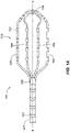
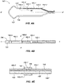
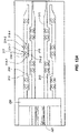
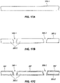
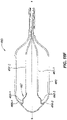
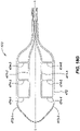
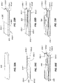
- Fig. 1A depicts a top view of a high density electrode mapping catheter 101 and Fig. 1B is an isometric side and top view of the high density electrode mapping catheter 101.
- the high density electrode mapping catheter 101 can include a flexible tip portion 110 that forms a flexible array of microelectrodes 102.
- This planar array (or 'paddle' configuration) of microelectrodes 102 comprises four side-by-side, longitudinally-extending arms 103, 104, 105, 106, which can form a flexible framework on which the microelectrodes 102 are disposed.
- the four microelectrode-carrier arms comprise a first outboard arm 103, a second outboard arm 106, a first inboard arm 104, and a second inboard arm 105. These arms can be laterally separated from each other.
- Each of the four arms can carry a plurality of microelectrodes 102.
- each of the four arms can carry microelectrodes 102 spaced along a length of each of the four arms.
- the catheters can include more or fewer than 18 electrodes.
- the first outboard arm 103 and second outboard arm 106 can include more or fewer than 5 microelectrodes and the first inboard arm 104 and second inboard arm 105 can include more or fewer than 4 microelectrodes).
- the microelectrodes 102 can be used in diagnostic, therapeutic, and/or mapping procedures.
- the microelectrodes 102 can be used for electrophysiological studies, pacing, cardiac mapping, and ablation.
- the microelectrodes 102 can be used to perform unipolar or bipolar ablation. This unipolar or bipolar ablation can create specific lines or patterns of lesions.
- the microelectrodes 102 can receive electrical signals from the heart, which can be used for electrophysiological studies.
- the microelectrodes 102 can perform a location or position sensing function related to cardiac mapping.
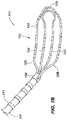
- the high density electrode mapping catheter 101 can include a catheter shaft 107.
- the catheter shaft 107 can include a proximal end and a distal end.
- the distal end can include a connector 108, which can couple the distal end of the catheter shaft 107 to a proximal end of the planar array.
- the catheter shaft 107 can define a catheter shaft longitudinal axis aa, as depicted in Fig. 1A , along which the first outboard arm 103, first inboard arm 104, second inboard arm 105, and second outboard arm 106 can generally extend parallel in relation therewith.
- the catheter shaft 107 can be made of a flexible material, such that it can be threaded through a tortuous vasculature of a patient.
- the catheter shaft 107 can include one or more ring electrodes 111 disposed along a length of the catheter shaft 107.
- the ring electrodes 111 can be used for diagnostic, therapeutic, and/or mapping procedures, in an example.
- the flexible tip portion 110 can be adapted to conform to tissue (e.g., cardiac tissue).
- tissue e.g., cardiac tissue
- the flexible tip portion can deflect, allowing the flexible framework to conform to the tissue.
- the arms (or the understructure of the arms) comprising the paddle structure (or multi-arm, electrode-carrying, flexible framework) at the distal end of the catheters depicted in Figs. 1A and 1B are preferably constructed from a flexible or spring-like material such as Nitinol and/or a flexible substrate, as discussed herein.
- the construction (including, for example, the length and/or diameter of the arms) and material of the arms can be adjusted or tailored to be created, for example, desired resiliency, flexibility, foldability, conformability, and stiffness characteristics, including one or more characteristics that may vary from the proximal end of a single arm to the distal end of that arm, or between or among the plurality of arms comprising a single paddle structure.
- the foldability of materials such as Nitinol and/or flexible substrate provide the additional advantage of facilitating insertion of the paddle structure into a delivery catheter or introducer, whether during delivery of the catheter into the body or removal of the catheter from the body at the end of a procedure.
- the disclosed catheters are useful to (1) define regional propagation maps of particularly sized areas (e.g., one centimeter square areas) within the atrial walls of the heart; (2) identify complex fractionated atrial electrograms for ablation; (3) identify localized, focal potentials between the microelectrodes for higher electrogram resolution; and/or (4) more precisely target areas for ablation.
- These mapping catheters and ablation catheters are constructed to conform to, and remain in contact with, cardiac tissue despite potentially erratic cardiac motion. Such enhanced stability of the catheter on a heart wall during cardiac motion provides more accurate mapping and ablation due to sustained tissue-electrode contact.
- the catheters described herein may be useful for epicardial and/or endocardial use.
- the planar array embodiments depicted herein may be used in an epicardial procedure where the planar array of microelectrodes is positioned between the myocardial surface and the pericardium.
- the planar array embodiments may be used in an endocardial procedure to quickly sweep and/or analyze the inner surfaces of the myocardium and quickly create high-density maps of the heart tissue's electrical properties.
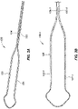
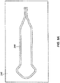
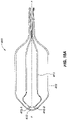
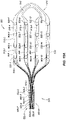
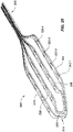
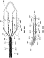
- Fig. 2A is an isometric side and top view of an inboard understructure 120 (also referred to herein as inner understructure) of a high density electrode mapping catheter in Fig. 1A .
- the inboard understructure 120 can be formed from a flexible or spring-like material such as Nitinol and/or a flexible substrate, as discussed herein.
- the inboard understructure 120 can include a first inboard arm understructure 121 and a second inboard arm understructure 122.
- the outboard understructure also referred to herein as outer understructure
- the outboard understructure also referred to herein as outer understructure that provides the understructure for the first outboard arm 103 and the second outboard arm 106 can be formed and/or processed in a manner analogous to that discussed in relation to the inboard understructure 120.
- the high density electrode mapping catheter includes additional arms, those arms can be formed and/or processed in a manner analogous to that discussed in relation to the inboard understructure 120.
- the inboard understructure 120 can include a first inboard mounting arm 123 and a second inboard mounting arm 124.
- the inboard mounting arms can be inserted into a distal end of the catheter 107 and through the connector 108 and can be used to connect the flexible tip portion 110 to the distal end of the catheter 107.
- the inboard mounting arms can be inserted through a torsional spacer, as discussed herein.
- the inboard understructure 120 (and although not depicted, the outboard understructure) can be formed from a planar piece of material. However, in some embodiments, the inboard understructure 120 (and the outboard understructure) can be formed from a cylindrical, square, or other shape of understructure. The inboard understructure 120 and the outboard understructure can be formed from a single unitary piece of material, as discussed in relation to Figs. 18A to 18G .
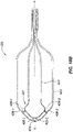
- Fig. 2B depicts an isometric side and top view of a coated inboard understructure 122-1 of a high density electrode mapping catheter 101.
- High density electrode mapping catheters can be assembled using tubular subassemblies for the inboard understructure and the outboard understructure.
- One reason for the use of tubing when assembling the understructures is to allow wire to be threaded through the tubing for connection of each individual microelectrode. This process can be labor and/or cost intensive, since each wire may be individually threaded through the tubing and individually connected with each microelectrode. Further, ensuring that a reliable electrical connection is established between each microelectrode and its wire can be challenging.
- a plurality of patterned conductive traces can be disposed on a flexible framework of an expandable structure.
- the plurality of patterned conductive traces can be disposed on a flexible framework of an expandable medical device structure.
- the patterned conductive traces can be electrically coupled with the plurality of microelectrodes 102 disposed on the flexible tip portion 110.
- the patterned conductive traces can be formed via a process that is less labor and/or cost intensive than current practices. Some examples can provide a means for testing an electrical connection between the microelectrodes 102 and the patterned conductive traces and/or wires, which electrically connect the plurality of microelectrodes 102.
- the inboard understructure can be coated with a dielectric material.
- the dielectric material can include parylene.
- Other dielectric materials such as a polyimide (e.g., PI-2771 or HD-4004 available from HD Microsystems) and/or an epoxy (e.g., SU8 epoxy available from MicroChem Corp), etc. can be used in accordance with design and end-use requirements.
- the understructure is an electrically conductive material
- the dielectric can electrically insulate the conductive traces, as discussed herein, from the electrically conductive material.
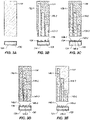
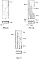
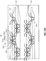
- Figs. 3A to 3K depict a top view and end view of a second inboard arm of the high density electrode mapping catheter and associated processing steps (the top view is depicted above the end view in Figs. 3A to 3K ).
- Fig. 3A depicts a conductive flexible framework 130 of the inboard understructure 120 coated with a dielectric material 131.
- the dielectric material can be applied to the conductive flexible framework 130 to coat the conductive flexible framework 130 in the dielectric material 131 to provide an electrically insulative layer, upon which patterned conductive traces can be disposed.
- Fig. 3B depicts the conductive flexible framework 130 of the inboard understructure 120 (also referred to as flexible framework) coated with the dielectric material 131 and a mask 134 (also referred to as masked portion).
- One or more unmasked trace pattern portions 132-1, 132-2, 132-3 can be formed on the dielectric coating of the conductive flexible framework 130 via the mask 134.
- the mask 134 can form channels 136 along the dielectric material, in which a conductive material can be deposited to form the electrically conductive traces.
- Fig. 3C depicts seed layers 138-1, 138-2, 138-3 deposited in the unmasked trace pattern portions 132-1, 132-2, 132-3 of Fig. 3B .
- the seed layers can be deposited within the channels 136 to partially fill the channels with the seed layers 138-1, 138-2, 138-3.
- the seed layers 138-1, 138-2, 138-3 can include copper (Cu), nickel (Ni), aluminum (Al), etc.
- the seed layers 138-1, 138-2, 138-3 can provide a base layer upon which a layer of conductive material can be deposited.
- the seed layers 138-1, 138-2, 138-3 can provide an interface between the dielectric material 131 and a conductive material which is deposited on the conductive flexible framework 130 to form electrically conductive traces.
- the seed layer can allow for the conductive material to be adhered to the dielectric material 131 (e.g., the conductive material is adhered to the dielectric material 131 via the seed layers 138-1, 138-2, 138-3).
- Fig. 3D depicts the seed layers 138-1, 138-2, 138-3 being plated with a conductive material (e.g., copper) to form electrically conductive traces 140-1, 140-2, 140-3.
- a conductive material e.g., copper
- the conductive material is deposited on the seed layers 138-1, 138-2, 138-3 and is thus adhered to the dielectric material 131. However, because the portions surrounding the electrically conductive traces 140-1, 140-2, 140-3 are masked, the conductive material is not deposited in those locations.
- Fig. 3E depicts the conductive flexible framework 130 coated with the dielectric 131 and the electrically conductive traces 140-1, 140-2, 140-3.
- the masked portion 134 can be stripped, leaving the electrically conductive traces 140-1, 140-2, 140-3 exposed on the dielectric material 131 that coats the conductive flexible framework 130.
- the dielectric material 131 can insulate the electrically conductive traces 140-1, 140-2, 140-3 from the conductive flexible framework 130, thus preventing shorts from occurring between the electrically conductive traces 140-1, 140-2, 140-3.
- Fig. 3F depicts the conductive flexible framework 130 coated with an additional layer of dielectric material 141.
- the additional layer of dielectric material 141 can be deposited over the initial layer of dielectric material 131 and over the electrically conductive traces 140-1, 140-2, 140-3.
- the additional layer of dielectric material 141 may only be deposited on the side of the conductive flexible framework 130 upon which the electrically conductive traces 140-1, 140-2, 140-3 are disposed.
- Fig. 3G depicts the conductive flexible framework 130 after the additional layer of dielectric material 141 has been stripped from a distal portion of each of the electrically conductive traces 140-1, 140-2, 140-3, leaving an exposed area 142-1, 142-2, 142-3.
- Laser ablation can be used to strip the distal portion of each of the electrically conductive traces 140-1, 140-2, 140-3 to create the exposed area 142-1, 142-2, 142-3.
- the additional layer of dielectric material can be removed via laser ablation.
- the exposed area 142-1, 142-2, 142-3 can be formed using photo-definable dielectric materials, wherein the exposed area 142-1, 142-2, 142-3 is masked and the dielectric material is patterned over the masked area.
- the photo-definable dielectric material can be developed and the masked material can be stripped to generate the exposed area 142-1, 142-2, 142-3.
- Fig. 31 depicts mask defined areas 143-1, 143-2, 143-3 on the conductive flexible framework 130.
- a mask material e.g., masked portions 144-1, 144-2, 144-3 can be a photo-definable mask material, wherein the mask material can be patterned over the masked portions 144-1, 144-2, 144-3 and developed to generate the masked portions 144-1, 144-2, 144-3.
- the masked portions can be located proximally and distally with respect to the distal portion of each of the plurality of conductive traces 140-1, 140-2, 140-3 (and the exposed areas 142-1, 142-2, 142-3) to form the mask defined areas 143-1, 143-2, 143-3.
- Fig. 3J depicts seed layers 145-1, 145-2, 145-3 deposited on the mask defined areas 143-1, 143-2, 143-3.
- the seed layers 145-1, 145-2, 145-3 can be deposited within the mask defined areas.
- the seed layers 145-1, 145-2, 145-3 can include copper (Cu), nickel (Ni), aluminum (Al), etc.
- the seed layers 145-1, 145-2, 145-3 can provide a base layer upon which a layer of conductive material can be deposited.
- the seed layers 145-1, 145-2, 145-3 can provide an interface between the additional layer of dielectric material 141 and the distal portion of the electrically conductive traces 140-1, 140-2, 140-3 and subsequently applied conductive material that forms the microelectrodes 102.
- the seed layer can allow for the conductive material that forms the microelectrodes to be adhered to the additional dielectric material 141.
- the distal portion of the electrically conductive traces 140-1, 140-2, 140-3 can provide an interface between the additional layer of dielectric material 141 and the distal portion of the electrically conductive traces 140-1, 140-2, 140-3 and subsequently applied conductive material that forms the microelectrodes 102.
- Fig. 3K depicts microelectrodes 146-1, 146-2, 146-3 that have been formed on the conductive flexible framework 130 via a plating process, according to various embodiments of the present disclosure.
- the seed layers 145-1, 145-2, 145-3 can be plated with a conductive material to form the microelectrodes 146-1, 146-2, 146-3.
- the conductive material that is used to form the microelectrodes 146-1, 146-2, 146-3 can include platinum iridium (Pt-Ir) in some embodiments.
- the platinum iridium coating process can be performed as described in Rao, Chepuri R.K.
- the conductive material can be plated circumferentially around the flexible framework 130.
- the conductive material can extend circumferentially around one of the first and second inboard arm understructures 121, 122.
- the seed layers 145-1, 145-2, 145-3, as well as the masked portions 144-1, 144-2, 144-3 can extend circumferentially around the first and second inboard arm understructures 121, 122, such that the conductive material can be plated circumferentially around the flexible framework 130.
- the microelectrodes 146-1, 146-2, 146-3 can be formed as ring electrodes that are axial with a respective one of the first inboard arm understructure 121 and the second inboard arm understructure 122.
- Fig. 3L depicts the dielectric 131 coated conductive flexible framework 130 that includes the additional layer of dielectric material 141, electrically conductive traces 140-1, 140-2, 140-3, and the microelectrodes 146-1, 146-2, 146-3.
- the masked portions 144-1, 144-2, 144-3 can be stripped, thus exposing the dielectric coated electrically conductive traces 140-1, 140-2, 140-3 on the dielectric 131 coated conductive flexible framework 130.
- the microelectrodes 146-1, 146-2, 146-3 can be electrically coupled to each respective electrically conductive trace 140-1, 140-2, 140-3, while remaining insulated from one another as a result of the additional dielectric material 141 that coats the electrically conductive traces 140-1, 140-2, 140-3.
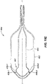
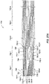
- Fig. 4A depicts a top view of a processed inboard understructure 160.
- Fig. 4B depicts an enlarged portion (indicated by dotted oval 4B) of a first inboard arm 164 of the processed inboard understructure depicted in Fig. 4A , according to various embodiments of the present disclosure.
- the processed inboard understructure 160 can be have a dielectric coating 161 that coats a conductive flexible framework (e.g., conductive flexible framework 130) of the processed inboard understructure 160.
- the dielectric coating 161 can be disposed between each of a plurality of patterned conductive traces 162-1, 162-2, 162-2 and the conductive flexible framework.
- the dielectric coating 161 can insulate the patterned conductive traces 162-1, 162-2, 162-2 from the conductive flexible framework, thus preventing a short from occurring between the patterned conductive traces 162-1, 162-2, 162-2.
- a first patterned conductive trace 162-1 can be electrically coupled to a first microelectrode 163-1; a second patterned conductive trace 162-2 can be electrically coupled to a second microelectrode 163-2; and a third patterned conductive trace 162-3 can be electrically coupled to a third microelectrode 163-3.
- the plurality of microelectrodes 163-1, 163-2, 163-3 can be arranged in a group.
- the plurality of microelectrodes 163-1, 163-2, 163-3 disposed along the first inboard arm 164 can be arranged in a respective group of three microelectrodes, as depicted in Fig. 4A , although more or fewer than three microelectrodes 163-1, 163-2, 163-3 can be arranged in a group along the first inboard arm 164.
- groups of microelectrodes can be arranged along the second inboard arm 165, along the first outboard arm, and/or along the second outboard arm, as depicted in Fig. 1A .
- the high density electrode mapping catheter 101 can include more than or fewer than four arms.
- the plurality of groups of microelectrodes can be arranged in respective rows of longitudinally aligned microelectrodes that are aligned parallel to a catheter shaft longitudinal axis a'a'.
- the plurality of patterned conductive traces 162-1, 162-2, 162-2 can be aligned parallel to the catheter shaft longitudinal axis a'a', depicted in Fig. 1A .
- Fig. 4C depicts a cross-sectional view of the first outboard arm 164 along the line cc, in Fig. 4B , according to various embodiments of the present disclosure.
- Fig. 4D depicts a cross-sectional view of the first outboard arm 164 along line dd, in Fig. 4B .
- the first outboard arm 164 includes the conductive flexible framework 165 that has been coated with a dielectric material 166', 166".
- the conductive flexible framework 165 can be coated with an upper layer of dielectric material 166' and a lower layer of dielectric material 166".
- the conductive flexible framework 165 can be coated circumferentially with the dielectric material, as discussed herein, such that microelectrodes that are circumferentially and coaxially disposed around the conductive flexible framework 165 are insulated from the conductive flexible framework 165, preventing short circuiting between multiple microelectrodes disposed on the conductive flexible framework 165.
- a first patterned conductive trace 162-1 can be disposed on top of the upper layer of dielectric material 166' and can be electrically coupled with the first microelectrode 163-1' via an exposed area located at a distal portion of the first patterned conductive trace 162-1, as discussed herein.
- the first microelectrode 163-1' can be coupled to the first patterned conductive trace 162-1 by plating a masked defined area (e.g., mask defined area 145-3), as discussed in relation to Figs. 31 to 3L .
- the first microelectrode 163-1' can contact the exposed area 168 (e.g., exposed area 142-3) of the first patterned conductive trace 162-1, thus electrically coupling the first patterned conductive trace 162-1 with the first microelectrode 163-1'.
- the first microelectrode 163-1' can be electrically coupled to the exposed area 168 of the first patterned conductive trace 162-1 at a location that is proximal to a distal end 167 of the first patterned conductive trace 162-1.
- the second patterned conductive trace 162-2 (and third patterned conductive trace 162-3, which is obscured by the second patterned conductive trace 162-2) can extend distally with respect to the first microelectrode 163-1' and can be electrically coupled with the second microelectrode 163-2 (and third microelectrode 163-3).
- the second patterned conductive trace 162-2 (and the third patterned conductive trace 162-3) can be electrically insulated from the first microelectrode 163-1' via an additional layer of dielectric material 169, as discussed herein.
- the processed inboard understructure 160 is depicted as including a single layer of patterned conductive traces 162-1, 162-2, 162-3.
- the processed inboard understructure 160 can multiple layers of patterned conductive traces. This can be desirable where an increased number of microelectrodes are placed on one or more of the inboard arms and/or outboard arms; a width of the frame is decreased, thus decreasing an area for placement of the patterned conductive traces; and/or a width of the patterned conductive traces is increased (e.g., due to a material selection associated with the traces).
- a width of the arms may not be sufficient such that the patterned conductive traces are adequately separated from one another to prevent cross-talk and/or shorting between the patterned conductive traces.
- multiple layers of patterned conductive traces can be formed on the arms, each layer being separated from one another by a dielectric material.
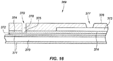
- each patterned conductive trace and an associated microelectrode can be made by filled vias, in some embodiments, for example, as discussed in relation to Fig. 16 .
- five patterned conductive traces and associated microelectrodes can be formed in a single layer of patterned conductive traces and along a single arm using a 0.001 inch (0,0254 mm) line (e.g., conductive trace) and space (e.g., spacing between the conductive traces) substrate design.
- each of the patterned conductive traces can be 0.001 inches (0,0254 mm) wide and each patterned conductive trace can be spaced 0.001 inches (0,0254 mm) away from an adjacent patterned conductive trace.
- patterned conductive traces can be employed and/or additional traces can be formed on an opposite side of the conductive flexible framework, as depicted in Fig. 5 .
- Fig. 5 depicts a cross-sectional view of patterned conductive traces formed on a top and bottom of a conductive flexible framework.
- a conductive flexible framework 180 can be coated with a dielectric material, as discussed herein.
- the dielectric material can be disposed between patterned conductive traces 181-1, 181-2, 181-3, 181-4 and the conductive flexible framework 180, which can serve to insulate the patterned conductive traces 181-1, 181-2, 181-3, 181-4 from the conductive flexible framework 180.
- One or more patterned conductive traces can be formed on a top of the conductive flexible framework 180 (e.g., patterned conductive traces 181-1, 181-2) and one or more patterned conductive traces can be formed on a bottom of the conductive flexible framework 180 (e.g., patterned conductive traces 181-3, 181-4) in a manner analogous to that discussed in relation to Figs. 3A to 3L .
- four microelectrodes can be disposed along the conductive flexible framework 180.
- a first microelectrode 182 can be disposed proximally with respect to a second microelectrode 183, in some embodiments.
- Fig. 6A depicts the conductive flexible framework 130' after the additional layer of dielectric material 141' has been stripped from a distal portion of each of the electrically conductive traces 140-1', 140-2', 140-3', leaving an exposed area 142-1', 142-2', 142-3'.
- process steps associated with Figs. 3A to 3G can be performed to arrive at the embodiment depicted in Fig. 6A .
- solder can be deposited on the distal portions of each of the electrically conductive trace (e.g., traces 140-1', 140-2', 140-3').
- FIG. 6B depicts a processed conductive flexible framework 199 after the additional layer of dielectric material 141' has been stripped from a distal portion of each of the electrically conductive traces 140-1', 140-2', 140-3', leaving an exposed area 142-1', 142-2', 142-3' on which solder 191-1, 191-2, 191-3 has been deposited.
- Fig. 6C depicts a cross-sectional end view of the processed conductive flexible framework 199 depicted in Fig. 6B along the line ee.
- Fig. 6D depicts a hollow cylindrical band 200.
- Fig. 6E depicts a hollow cylindrical band 203 in which solder 208 is deposited, according to various embodiments of the present disclosure.
- Fig. 6F depicts an isometric side and front view of the hollow cylindrical band 200 depicted in Fig. 6D .
- the hollow cylindrical band 200 can be the same or similar to the hollow cylindrical band 203 depicted in Fig. 6E .
- the hollow cylindrical band 200 can include a split 201, which can extend longitudinally down a sidewall of the hollow cylindrical band. Although, as depicted in Fig. 6D (and Fig. 6F ), the split 201 extends parallel with a longitudinal axis of the hollow cylindrical band 200, the split 201 can be divergent with the longitudinal axis of the hollow cylindrical band 200.
- the hollow cylindrical band 200 can be coaxially aligned with the processed conductive flexible framework 199.
- the hollow cylindrical band 200 can be slipped over a proximal end of an arm of the processed conductive flexible framework 199 into position over the solder 191-1.
- the hollow cylindrical band 200 can be placed over the solder 191-1 such the solder 191-1 is aligned with the hollow cylindrical band 200 between a proximal end and a distal end of the hollow cylindrical band 200.
- a circumferential width of the split 201 in the hollow cylindrical band 200 (defined by line gg in Fig. 6D ) can be greater than a height of the processed conductive flexible framework (defined by line ff in Fig.
- the hollow cylindrical band 200 e.g., the slit 201 of the hollow cylindrical band 200
- the hollow cylindrical band 200 can be laterally slid over the processed conductive flexible framework 199, instead of being slipped over a proximal end of the arm of the processed conductive flexible framework 199.
- Fig. 6H depicts a processing step associated with the hollow cylindrical band 200.
- the hollow cylindrical band 200 can be coaxially aligned with the processed conductive flexible framework 199 and the solder 191-1 can be aligned with the hollow cylindrical band 200 between a proximal end and a distal end of the hollow cylindrical band 200.
- the hollow cylindrical band 200 can be swaged onto the processed conductive flexible framework 199.
- a force can be applied to the hollow cylindrical band 200 in a direction of at least one of the arrows (e.g., arrow 205) to swage the hollow cylindrical band 200 onto the processed conductive flexible framework 199.
- Fig. 6I depicts the swaged hollow cylindrical band 206 after the processing step described in relation to Fig. 6H .
- a circumferential width of the split 202 can be decreased as a result of the swaging process and the swaged hollow cylindrical band 206 can contact portions of the processed conductive flexible framework 199 (e.g., the corners of the processed conductive flexible framework 199 and the solder 191-1).
- Fig. 6J depicts the swaged hollow cylindrical band 206 and the processed conductive flexible framework 199 after a solder reflow process.
- a reflow process can be performed to reflow the solder depicted in Fig. 6I , such that the reflowed solder 207 is distributed and contacts both the swaged hollow cylindrical band 206 and the processed conductive flexible framework 199.
- the solder 207 can connect the swaged hollow cylindrical band 206 and the processed conductive flexible framework 199 and can electrically couple the electrically conductive trace 140-1 and the swaged hollow cylindrical band 206.
- the swaged hollow cylindrical band 206 forms the microelectrode, as discussed herein.
- solder e.g., solder 191-1
- solder 191-1 may or may not be placed on the exposed area 142-1', 142-2', 142-3' of the electrically conductive traces 140-1', 140-2', 140-3'.
- the hollow cylindrical band 203 can be placed over the processed conductive flexible framework 199 such that the solder 208 is in close proximity to the exposed area 142-1', 142-2', 142-3' of the electrically conductive traces 140-1', 140-2', 140-3'.
- 6G-6J can be performed to swage the hollow cylindrical band 203 and reflow the solder 208 to establish a connection between the hollow cylindrical band 203 and the processed conductive flexible framework 199 and an electrical connection between the hollow cylindrical band 203 and the electrically conductive trace 140-1'.
- Solder can be deposited on the hollow cylindrical band 203 and the exposed area 142-1', 142-2', 142-3' of the electrically conductive traces 140-1', 140-2', 140-3' to allow for an increased distribution of solder in the reflowing process.
- Fig. 7A depicts a top view and end view of a second inboard arm of the high density electrode mapping catheter, wherein a flexible framework 220 of the high density electrode mapping catheter is formed from a flexible substrate and associated processing steps (the top view is depicted above the end view in Figs. 7A to 7C ).
- the flexible framework 220 can be formed from a flexible substrate.
- the flexible substrate can include for example, those discussed in relation to Fig. 11 .
- the flexible substrate can include a printed circuit board.
- the printed circuit board can be formed from a fiberglass and/or a plastic, which does not conduct electricity.
- the printed circuit board can be formed from a polymer.
- the flexible substrate 220 can be coated with a conductive material 222.
- the conductive material 222 can include Cu, for example, although other conductive materials can be used.
- Fig. 7B depicts a top view and end view of the second inboard arm of the high density electrode mapping catheter, wherein a mask layer is deposited on the conductive material 222 coating the flexible framework 220 to form a masked trace pattern 223-1, 223-2, 223-3 on the coated flexible framework and an unmasked portion.
- the surrounding areas of the masked trace pattern 223-1, 223-2, 223-3 include the uncoated conductive material 222.
- Fig. 7C depicts a top view and end view of the second inboard arm of the high density electrode mapping catheter, wherein the surrounding areas of the masked trace pattern 223-1, 223-2, 223-3 have been stripped of the conductive material 222.
- the conductive material 222 can be stripped such that the flexible substrate 220 that surrounds the masked trace pattern 223-1 is exposed.
- the masked trace pattern 223-1, 223-2, 223-3 has also been stripped thus exposing electrically conductive traces 224-1, 224-2, 224-3.
- the electrically conductive traces 224-1, 224-2, 224-3 can be directly connected with the flexible substrate 220, which is electrically insulative. Accordingly, the electrically conductive traces 224-1, 224-2, 224-3 can be electrically insulated from one another, thus preventing short circuits from occurring between the electrically conductive traces 224-1, 224-2, 224-3.
- a dielectric coating can be deposited on the electrically conductive traces 224-1, 224-2, 224-3 as well as the flexible substrate 220 and exposed areas of the electrically conductive traces 224-1, 224-2, 224-3 can be formed.
- Fig. 8A depicts a top view of a processed inboard understructure 228, according to various embodiments of the present disclosure.
- Fig. 8B depicts an enlarged portion (indicated by dotted oval 8B) of a first inboard arm 230 of the processed inboard understructure 228 depicted in Fig. 8A .
- the processed inboard understructure 228 includes a first inboard arm 230 and a second inboard arm 231.
- the processed inboard understructure 228 can be formed from a flexible substrate, as discussed herein.
- the flexible substrate include a printed circuit board and/or polymer.
- the flexible substrate can be coated with a dielectric material 232, in some embodiments.
- the first inboard arm 230 of the processed inboard understructure 228 includes electrically conductive traces 224-1, 224-2, 224-3 and microelectrodes 227-1, 227-2, 227-3.
- a first electrically conductive trace 224-1 can be electrically coupled to a first microelectrode 227-1;
- a second electrically conductive trace 224-2 can be electrically coupled to a second microelectrode 227-2;
- a third electrically conductive trace 224-3 can be electrically coupled to a third microelectrode 227-3.
- the second inboard arm 231 of the processed inboard understructure 228 includes electrically conductive traces 226-1, 226-2, 226-3 and microelectrodes 229-1, 229-2, 229-3.
- a first electrically conductive trace 226-1 can be electrically coupled to a first microelectrode 229-1; a second electrically conductive trace 226-2 can be electrically coupled to a second microelectrode 229-2; and a third electrically conductive trace 226-3 can be electrically coupled to a third microelectrode 229-3.
- Fig. 8C depicts an enlarged portion (indicated by dotted oval 8C) of the first inboard arm 230 of the processed inboard understructure 228 depicted in Fig. 8A .
- Fig. 8C depicts the first electrically conductive trace 224-1 electrically coupled to a first proximal termination contact pad 235-1; the second electrically conductive trace 224-2 electrically coupled to a second proximal termination contact pad 235-2; and the third electrically conductive trace 224-3 electrically coupled to a third proximal termination contact pad 235-3.
- the proximal termination contact pads are not depicted in Fig. 8A .
- the flexible framework of the flexible tip portion 110 of the high density electrode mapping catheter 101 can include the proximal termination contact pads.
- each arm of the inboard understructure and/or each arm of the outboard understructure (and/or additional understructures not shown) can include the proximal termination contact pads along a proximal portion of the inboard understructure and/or outboard understructure.
- the proximal termination contact pads 235-1, 235-2, 235-3 can provide electrical connection points for electrically connecting the microelectrodes (e.g., microelectrodes 227-1, 227-2, 227-3).
- the proximal termination contact pads 235-1, 235-2, 235-3 can provide an increased area for an electrical connection to be made with each of the electrically conductive traces 224-1, 224-2, 224-3 and thus each of the microelectrodes 227-1, 227-2, 227-3.
- the proximal termination contact pads 235-1, 235-2, 235-3 can be used to electrically test continuity between each of the electrically conductive traces and respective microelectrodes.
- each of the proximal termination contact pads can be probed with an electrical testing device to ensure that an uninterrupted electrical connection exists between each of the proximal termination contact pads, a respective one of the electrically conductive traces, and a respective microelectrode.
- the proximal termination contact pads can provide an increased area for probing with the electrical testing device (e.g., versus proving each individual electrically conductive trace).
- Fig. 9A depicts a top view of a bottom mold 245 for an overmolding process.
- the bottom mold 245 includes a mold cavity 246, which can be size and configured to accept an understructure (e.g., processed understructure) of the flexible tip portion 110. Different molds can be used for the outboard understructure and the inboard understructure (and additional understructures if included).
- the bottom mold 245 can be sized and configured to accept the processed inboard understructure 160 and/or the processed inboard understructure 228 in the mold cavity 246, as depicted in Fig. 9B .
- Fig. 9B depicts a top view of a processed inboard understructure 228 inserted into the bottom mold 245.
- the processed inboard understructure 228 depicted in Fig. 8A is depicted as being inserted in the mold cavity 246 of the bottom mold 245.
- Fig. 9C depicts a cross-sectional side view of an assembled mold 250 along line hh in Fig. 9B .
- Fig. 9C depicts a top mold 247 and the bottom mold 245 in a closed position, thus enclosing the processed inboard understructure 228 (consisting of distal portion 228-1 of the processed inboard understructure 228 and proximal portion 228-2 of the processed inboard understructure 228) in the mold cavity and forming assembled mold 250.
- the assembled mold 250 includes a bottom mold cavity 246.
- the cross-sectional view of the bottom mold cavity 246 depicts a distal bottom mold cavity 246-1 and a proximal bottom mold cavity 246-2.
- the bottom mold cavity 246 can be formed in the bottom mold 245.
- the assembled mold 250 includes a top mold cavity 248.
- the cross-sectional view of the top mold cavity 248 depicts a distal top mold cavity 248-1 and a proximal top mold cavity 248-2.
- the top mold cavity 248 can be formed in the top mold 247 of the assembled mold 250.
- the bottom mold 245 and the top mold 247 can include standoffs (not shown) that extend into the bottom mold cavity 246 and the top mold cavity 248 to position the processed inboard understructure 228 a particular distance away from walls of the bottom mold 245 and the top mold 247 that form the bottom mold cavity 246 and the top mold cavity 248.
- the distance between the processed inboard understructure 228 and the walls of the bottom mold 245 and the top mold 247 can define a thickness of an overmolding that covers the understructure.
- the top mold 247 and/or the bottom mold 245 can include a port 249 configured for introduction of an overmolding material into the bottom mold cavity 246 and the top mold cavity 248.
- the assembled mold 250 can include a gate and runner system to help with distribution of the overmolding material into the bottom mold cavity 246 and the top mold cavity 248.
- the gate and runner system can be designed in accordance with rheological properties of an overmolding material.
- Fig. 9D depicts a top view of bottom mold 245 and an overmolded inboard understructure 260 after an overmolding process has been performed.
- Fig. 9E depicts a cross-sectional side view of an assembled mold and the overmolded inboard understructure in Fig. 9D along line ii in Fig. 9D .
- the processed inboard understructure 228 has been overmolded with an overmolding material 261.
- the overmolding material 261 is injected via the port 249 and fills the space existing between the processed inboard understructure 228 and the walls of the bottom mold 245 and the top mold 247 (e.g., assembled mold 250).
- the overmolding material 261 can include a polyether block amide (e.g., PEBAX ® available from Arkema).
- the overmolding material can be a polyurethane (e.g., Pellethane 2363-80A or 2363-90A, or Tecoflex EG93A or EG100A both available from Lubrizol Corp.) or other suitable materials having the required biocompatibility, elastomeric, and mechanical properties required by specific design and end-use requirements.
- Fig. 10A depicts a cross-sectional side view of an ablation fixture 270 in which the overmolded inboard understructure 260 has been placed.
- the ablation fixture 270 can include an ablation reference point 271, which can be referenced by an ablation tool.
- ablation reference point 271 can be referenced by an ablation tool.
- a location of the ablation reference point 271 is depicted as being proximal to the overmolded inboard understructure 260, the reference point 271 can be located distally with respect to the overmolded inboard understructure 260, and/or to either side of the overmolded inboard understructure 260.
- the ablation tool can be a laser and/or other type of ablation tool, which can reference the reference point 271 such that the overmolding material 261 covering (e.g., covering an outer surface of) the microelectrodes 229-1, 229-2, 229-3 can be accurately removed by the ablation tool.
- the reference point 271 can be located a particular distance away from each of the microelectrodes, represented by line jj, line kk, and line ll.
- the ablation tool can ablate the overmolding material 261 proximally and/or distally with respect to an end point of each of the lines to remove the overmolding material 261 from the outer surface of the microelectrodes 229-1, 229-2, 229-3.
- the ablation tool can be programmed to ablate at specific locations based on programmable instructions.
- a processor e.g., computer
- Fig. 10B depicts a top view of the ablation fixture 270 in Fig. 10A after an ablation processing step has been completed and an ablated overmolded inboard understructure 280.
- the overmolding material 261 has been removed from the microelectrodes 227-1, 227-2, 227-3, 229-1, 229-2, 229-3, thus exposing the microelectrodes 227-1, 227-2, 227-3, 229-1, 229-2, 229-3.
- Overmolding material 261 can be removed from the proximal termination contact pads 235 in a similar manner.
- a first side of the overmolded inboard understructure 260 can be ablated and can then be turned over so a second side of the partially ablated inboard understructure can be ablated.
- the overmolding material 261 can be circumferentially removed from the overmolded inboard understructure 260.
- Fig. 10C depicts a top view of the ablated overmolded inboard understructure 280 after being ejected from the ablation fixture 270.
- Fig. 11 depicts mechanical properties of various materials that can be used for forming understructures of the flexible tip portion 110.
- the understructure can be formed from a flexible material.
- the flexible material can be a super elastic material, such as Nitinol.
- Nitinol can include Nitinol available from NDC; Cu doped Nitinol available from Johnson Matthey Medical Components; Nitinol available from Fort Wayne Metals; and/or Nitinol available from Euroflex.
- the flexible material forming the understructure can include a flexible substrate.
- the understructures of the flexible tip portion 110 can be formed from a flexible substrate, such as a polymer and/or printed circuit board, as discussed herein.
- the flexible substrate can have mechanical properties that are similar to Nitinol.
- the flexible substrate can have an elastic modulus that is the same or similar to Nitinol; an ultimate tensile strength that is the same or similar to Nitinol; a loading plateau that is the same or similar to Nitinol; and/or a flexural strength that is the same or similar to Nitinol.
- the flexible substrate can include a liquid crystalline polymer (LCP) circuit material, such as Ultralam 3850HT available from Rogers Corporation; a glass microfiber reinforced polytetrafluoroethylene (PTFE) composite such as RT/duroid ® 5870/5880 available from Rogers Corporation; a glass-reinforced epoxy laminate (FR4) in accordance with IPC 4101C/21/24/26/121/124/129; a glass-reinforced epoxy laminate (FR4) in accordance with Characterization of the material properties of two FR4 printed circuit board laminates, E.T. Haugan and P. Dalsjo, Norwegian Defense Research Establishment (FFI), Report 10 Jan 2014; S1141 available from Shengyi Sci. Tech. Co. Ltd.
- LCP liquid crystalline polymer
- PTFE polytetrafluoroethylene
- FR408HR available from Isola Group
- BT Bismaleimide/Triazine
- epoxy resin blend such as BT G200 available from Isola
- BT Bismaleimide/Triazine
- N5000-32 available from Nelco ®
- the flexible tip portion 110 depicted in Figs. 1A and 1B can have an array buckling force of less than or equal to 200 grams of force.
- an amount of force less than or equal to 200 grams of force can be applied to the flexible tip portion.
- the flexible tip portion can be deflected as shown in Fig. 1B when an amount of force less than or equal to 200 grams of force has been applied to a distal end of the flexible tip portion, which can be formed from the materials discussed herein.
- Fig. 12A depicts a top view of a proximal end of an inboard understructure 290.
- the inboard understructure 290 can include frame locks 291-1, 291-2, 291-3, 291-4 on the proximal end of the inboard understructure 290.
- an outboard understructure can include frame locks that correspond with frame locks 291-1, 291-2, 291-3, 291-4 on the inboard understructure.
- Fig. 12B depicts a top view of an enlarged portion (indicated by dotted circle 12B) of frame locks 291-1, 291-2, 291-3, 291-4 depicted on a proximal end of the inboard understructure depicted in Fig. 12A .
- One or more electrical connections 292-1, 292-2, .... 292-8 can be disposed on one or more of the frame locks 291-1, 291-2, 291-3, 291-4 and/or on one of the arms of the understructure.
- the electrical connections 292-1, 292-2, .... 292-8 can be formed on a proximal portion of the arms of the understructure.
- Fig. 12C depicts a top view of an enlarged portion (indicated by dotted circle 12C) of electrical connections 292-3, 292-4 depicted in Fig. 12B .
- a third electrical connection 292-3 can include a distal contact pad 295-1 and a proximal contact pad 295-2 and a fourth electrical connection 292-4 can include a distal contact pad 295-4 and a proximal contact pad 295-3.
- the electrical connections can be disposed on the proximal portion of an understructure of the flexible tip portion 110.
- the electrical connections can be insulated from the understructure (e.g., where the understructure is electrically conductive) to prevent short circuiting from occurring between the electrical connections.
- the fourth electrical connection 295-4 the distal contact pad 295-4 and the proximal contact pad 295-3 can be electrically couple to one another via a trace 296-2.
- Fig. 12D depicts a cross-sectional view of Fig. 12C along line mm.
- the understructure 290 can be coated with a dielectric 297 material, such as parylene.
- the dielectric material 297 can electrically insulate the electrical connections from a conductive understructure 290, as discussed herein.
- a metallization can be completed on a surface of the dielectric, thus allowing for a secure connection between the electrical connection 292-4 to the understructure 290.
- a metal such as aluminum can be deposited on the surface of the dielectric material 297 and the electrical connection 292-4 can be disposed on top of the metal 298.
- Fig. 12E depicts a top view of wires electrically coupled via an electrical connection depicted in 12C.
- a distally running wire 300 and/or a proximally running wire 301 can be electrically coupled to the third electrical connection 292-3. 2.
- the distally running wire 300 and the proximally running wire 301 can be connected via the third electrical connection 292-3.
- the distally running wire 300 can be soldered to the distal contact pad 295-4 and/or the proximally running wire 301 can be soldered to the proximal contact pad 295-3.
- wires e.g., distally running wires
- wires can be electrically coupled with each of the microelectrodes.
- a proximal end of the distally running wires can be electrically coupled with distal contact pads of each of the electrical connections.
- the flexible tip portion 110 can be formed as a module, wherein the individual distally running wires are connected at a distal end to each of the microelectrodes and at a proximal end to a distal contact pad of the electrical connections.
- the proximal contact pad can be left open (e.g., a wire may not be electrically coupled to the proximal contact pad) such that the module can be tested.
- each of the proximal contact pads can be probed with an electrical testing device to establish that continuity exists and that a signal noise associated with each of the microelectrodes and associated distally running wire does not exceed a defined amount. This can be accomplished prior to assembling the entire high density electrode mapping catheter 101.
- the electrical connectors can decrease a complexity associated with connecting the proximally running wires and the distally running wires of the high density electrode mapping catheter 101.
- the proximal end of the distally running wire can be coupled with the distal pad of the electrical connection and the distal end of the proximally running wire can be coupled with the proximal pad of the electrical connection.
- a pre-made substrate e.g. flex substrate
- the pre-made substrate includes the electrical connections and can be bonded to the understructure (e.g., the parylene coated frame).
- the substrate design can copy the basic electrical connection configuration discussed and depicted in relation to Figs. 12B to 13B . This can allow for a microelectrode density to be increased on an array formed by the flexible tip portion 110 (e.g. increase number of microelectrodes from 22 to 32 to 64) by forming multilayer substrates.
- the pre-made substrate can be attached to the understructure using adhesive materials, such as epoxy.
- Fig 13A depicts a top view of a plurality of electrical connections disposed on an first inboard arm 310; second inboard arm 311, first outboard arm 312; and second outboard arm 313 of a flexible framework of a flexible tip portion 110 of the high density electrode mapping catheter 101.
- the plurality of electrical connections are generally discussed in relation to electrical connections 314-1, 314-2, 314-3, 314-4.
- the electrical connections can be disposed on frame locks (e.g., frame lock 315) and/or a proximal portion of the arms 310, 311, 312, 314.
- a number of electrical connections disposed on each frame lock can range from 1 to 10.
- each of the electrical connections can include a proximal contact pad and a distal contact pad electrically coupled by a trace 317.
- the first electrical connection 314-1 can include a distal contact pad 316-1 and a proximal contact pad 316-2 connected by a trace 317, as discussed herein.
- Distally extending wires for example distally extending wire 321 can extend distally along the flexible framework of the high density electrode mapping catheter 101. As depicted in Fig. 13 B , a proximal end of each of the distally extending wires can be electrically coupled to a distal contact pad (e.g., distal contact pad 316-1) of each of the electrical connections. Connection of the distal end of each of the distally extending wires can result in a single module that can be tested, as discussed herein.
- a distal contact pad e.g., distal contact pad 316-1
- Each of the arms can extend through a torsional spacer 320, which can be configured to maintain an alignment between the arms.
- An overmolding and ablation process can be employed, as discussed in relation to Figs. 9A to 10C , which can overmold each arm of the flexible framework (e.g., arms 310, 311, 312, 314) as well as the torsional spacer 320.
- the connector 108 depicted in Figs. 1A and 1B , can be overmolded as well.
- An overmolding material can include PEBAX ® as discussed herein.
- Fig. 13B depicts a top view of a portion of a subset of the electrical connections disposed on a first inboard arm 310; second inboard arm 311, first outboard arm 312; and second outboard arm 313 of a flexible framework of a flexible tip portion 110 of the high density electrode mapping catheter 101 depicted in Fig. 13A .
- the subset of electrical connections is generally discussed in relation to electrical connections 314-1, 314-2, 314-3, 314-4.
- a proximal end of each of a plurality of distally extending wires can be electrically coupled to a respective one of a plurality of distal contact pads of each of the plurality of electrical connections and a distal end of each of a plurality of proximally extending wires can be electrically coupled to a respective one of proximal contact pads of each of the plurality of electrical connections.
- distally extending wire 330 and proximally extending wire 331 can be electrically coupled to the distal contact pad 316-1 and the distal end of the proximally extending wire 331 can be electrically coupled to the proximal contact pad 316-2 of the electrical connection 314-2.
- the contact pads 316-1, 316-2 can be electrically coupled via the trace 317 as discussed herein, and thus the wires 330, 331 can be electrically coupled with one another.
- Fig. 14 depicts a method flow diagram 340 for a process for forming an integrated electrode structure that includes a conductive understructure.
- the method can include coating a flexible framework of a flexible tip portion of the integrated electrode structure with a first dielectric material at step 331.
- a trace pattern on the coated flexible framework can be masked with a masking material to form a masked portion and an unmasked trace pattern portion at step 332.
- a seed layer can be deposited on the unmasked trace pattern portion at step 333.
- the method can include plating the seed layer with a conductive material to form an electrically conductive trace at step 334.
- the method can include stripping the masking material from the masked portion.
- the method can include coating the electrically conductive trace with a second dielectric material at step 336.
- the method can include stripping the second dielectric material from a distal portion of the electrically conductive trace.
- the method can include electrically connecting a microelectrode to the distal portion of the electrically conductive trace at step 338. Electrically connecting the microelectrode to the distal portion of the electrically conductive trace can include masking the flexible framework of the integrated electrode structure proximally and distally with respect to the distal portion of the electrically conductive trace to form a mask defined area; depositing a second seed layer across the mask defined area; and plating the mask defined area with an electrically conductive material to form the microelectrode, as discussed herein.
- the method can include circumferentially masking the flexible framework of the integrated electrode structure proximally and distally with respect to the distal portion of the electrically conductive trace to form a circumferential mask defined area.
- the microelectrode may not be formed through a plating process (e.g., depositing a conductive material to form the microelectrode), rather a hollow cylindrical band can be electrically connected to the distal portion of the electrically conductive trace, wherein the hollow cylindrical band is coaxial with the flexible framework of the flexible tip portion.
- Electrically connecting the hollow cylindrical band to the distal portion of the electrically conductive trace can include depositing solder on the distal portion of the electrically conductive trace; coaxially aligning the hollow cylindrical band with the distal portion of the electrically conductive trace and the flexible framework; and reflowing the solder to electrically couple the hollow cylindrical band with the distal portion of the electrically conductive trace.
- Fig. 15 depicts a method flow diagram 350 for a process for forming an integrated electrode structure that includes a substrate understructure.
- the method can include coating a flexible framework substrate of a flexible tip portion of the integrated electrode structure with a conductive material at step 351.
- the flexible framework can be formed of a flexible substrate.
- the method can include masking a trace pattern on the coated flexible framework with a masking material to form a masked trace pattern portion and an unmasked portion at step 352.
- the method can include etching the unmasked portion to expose the flexible framework substrate.
- the method can include stripping the masking material from the masked trace pattern portion to expose an electrically conductive trace at step 354.
- the method can include coating the electrically conductive trace with a dielectric material at step 355.
- the method can include stripping the dielectric material from a distal portion of the electrically conductive trace at step 356.
- the method can include electrically connecting a microelectrode to the distal portion of the electrically conductive
- the method can further include overmolding the integrated electrode structure with a polymer such as PEBAX. ® .
- the overmolding can be removed from an outer surface of the microelectrode via a ablating step, as discussed herein.
- Fig. 16 depicts a side view of an arm 369 of the high density electrode mapping catheter.
- a dielectric material 371 can coat an understructure 370 of the arm 369 of the high density electrode mapping catheter.
- One or more electrically conductive traces 372 can be formed on an outer facing surface of the dielectric material 371 (facing away from the understructure 370), as discussed herein.
- a mask can be applied to the dielectric material 371 to form unmasked trace pattern portions.
- a seed layer can be applied to coat the unmasked trace pattern portions.
- the electrically conductive trace 372 can be formed on top of the seed layer, which can adhere the electrically conductive trace 372 to the dielectric material 371.
- Multiple layers of electrically conductive traces 372 can be formed on the arm 369 of the high density electrode mapping catheter, as depicted in Fig. 16 .
- One or more additional electrically conductive traces 373 can be formed on a second layer of dielectric material 374.
- the second layer of dielectric material 374 can be applied over the first layer of dielectric material 371 and over the electrically conductive trace 372.
- a first via 375 can be formed in the dielectric material 374 that coats the electrically conductive trace 372.
- a mask can be applied over a portion of the electrically conductive trace 372 (e.g., a portion where the via 375 will be formed) before the second layer of dielectric material 374 is applied and/or the second layer of dielectric material 374 can be removed to create the first via 375. Additional electrically conductive traces can be constructed in this manner.
- the additional electrically conductive trace 373 can be applied over a portion of the second layer of dielectric material 374.
- a distal end of the additional electrically conductive trace can be disposed proximally with respect to the first via 375.
- the additional electrically conductive trace 373 and the electrically conductive trace 372 can run parallel with respect to one another and parallel with respect to the understructure 370.
- a third layer of dielectric material 376 can coat a portion (e.g., outer facing surface) of the second layer of dielectric material 374 and the additional electrically conductive trace 373.
- a mask can be applied over the additional electrically conductive trace 373 (e.g., a portion where the via 377 will be formed) before the third layer of dielectric material 376 is applied and/or the third layer of dielectric material 376 can be removed to create the via 377 for the second electrically conductive trace 373.
- the mask applied to the electrically conductive trace 372 can be removed after application of the third layer of dielectric material 376, thus creating the first via 375 in the second layer of dielectric material 374 and a second via 378 in the third layer of dielectric material 376 to form via 379.
- multiple layers of electrically conductive traces 372, 373 can be formed on the understructure 370 of the arm 369. As discussed herein, this can be beneficial when a real estate associated with a surface of the arm 369 is not large enough to support formation of more than a particular number of electrically conductive traces next to one another. Accordingly, some examples of the present disclosure can allow for electrically conductive traces to be formed in different layers.
- a similar formation can be formed on another side of the understructure 370 of the arm 369.
- another side of the arm 369 e.g., opposite side of the arm 369 with respect to the electrically conductive traces 372, 373
- Figs. 17A to 17E depict a side view of an understructure of an arm of the high density electrode mapping catheter and associated processing steps.
- Fig. 17A depicts an understructure 385-1 associated with the arm of the high density electrode mapping catheter.
- a first via 386-1 and second via 386-2 can be formed in the understructure 385-2.
- the vias 386-1, 386-2 can be cut via a laser, drilled, etc.
- the understructure 385-2 can be coated with a first coating of dielectric material 387, such as parylene, for example.
- an electrically conductive trace 388 can be applied on the first coating of dielectric material 387 that coats the understructure 385-2.
- the electrically conductive trace 388 can be applied to a top surface and bottom surface associated with the first coating of dielectric material 387 that coats the understructure 352-2.
- the electrically conductive trace 388 can fill the via 386-2, thus electrically coupling a bottom portion of the electrically conductive trace 388 applied to the bottom surface associated with the first coating of dielectric material 387 and a top portion of the electrically conductive trace 388 applied to the top surface associated with the first coating of dielectric material 387.
- the electrically conductive trace 388 can extend proximally with respect to the via 386-2.
- the electrically conductive trace 388 can extend distally with respect to the second via 386-2.
- a distal end of the electrically conductive trace 388 can be disposed between the first via 386-1 and the second via 386-2.
- a second coating of dielectric material 390 can be applied to a top surface and bottom surface of the first coating of dielectric material 387 and the electrically conductive trace 388.
- the second coating of dielectric material 390 may not be applied to the first via 386-1 and/or can be removed from the first via 386-1.
- Fig. 17F depicts a processed understructure 392 that includes a second electrically conductive trace 391 applied to a top surface and bottom surface of the second coating of dielectric material 390. As depicted in Fig.
- the second electrically conductive trace 391 can be applied to the portions of the first coating of dielectric material 387 surrounding the first via 386-1, that are not coated with the second coating of dielectric material 390.
- the second coating of dielectric material 390 can be applied proximally and/or distally with respect to the first via 386-1, leaving the first coating of dielectric material 387 exposed for coating with the second electrically conductive trace 391.
- the second electrically conductive trace 391 can extend along a top portion and a bottom portion of processed understructure 392.
- the second electrically conductive trace 391 can extend through the via 386-1, thus electrically coupling portions of the second electrically conductive trace 391 extending along the top portion and the bottom portion of the processed understructure 392.
- the first electrically conductive trace 388 can be laterally offset from the second electrically conductive trace 391.
- a via can be formed in the second coating of dielectric material 390, which can be used to electrically connect a microelectrode or other device to the first electrically conductive trace 388, while electrically insulating the microelectrode or other device from the second electrically conductive trace 391.
- a third coating of dielectric material can be applied to the second electrically conductive trace 391 and a microelectrode can be electrically coupled with the second electrically conductive trace 391 through a via formed in the third coating of dielectric material.
- Figs. 18A to 18G depict top views of an understructure of a high density electrode mapping catheter in Fig. 1A .
- the examples depicted in Figs. 18A to 18G can be constructed from a unitary piece of material.
- Fig. 18A depicts an understructure 410 that includes an inner understructure 411 (also referred to herein as inboard understructure) and an outer understructure 412 (also referred to herein as outboard understructure), which can be formed from a single piece of material.
- the inner understructure 411 and the outer understructure 412 can be laser cut from a single piece of material and/or photo etched from a single piece of material.
- a distal end of the inner understructure 411 can be connected to a distal end of the outer understructure 412 via a connective portion 413.
- the connective portion 413 can be formed from the same unitary piece of material as the inner understructure 411 and the outer understructure 412.
- the connective portion 413 can extend from a distal side of the distal end of the inner understructure 411 to a proximal side of the distal end of the outer understructure 412.
- the connective portion 413 can be planar and can be equal in thickness with the inner understructure 411 and the outer understructure 412.
- the connective portion can extend between the distal end of the inner understructure 411 and the distal end of the outer understructure 412 on either side of an understructure longitudinal axis nn defined by the inner understructure 411 and the outer understructure 412, which is depicted in Fig. 18A .
- outer edges 415-1, 415-2 can be radiused toward the understructure longitudinal axis nn.
- the radiused outer edges 415-1, 415-2 can help with minimizing strain existing between the inner understructure 411 and the outer understructure 412, as the understructure 410 is inserted and/or deployed from a sheath.
- the portions of the inner understructure 411 and the outer understructure 412 located adjacent to the outer edges of the connective portion 413 can experience an increased strain.
- the radiused outer edges 415-1, 415-2 can better distribute the strain as the understructure 410 is deflected and/or inserted into or deployed from the sheath.
- Fig. 18B depicts an understructure 420 that includes an inner understructure 421 and an outer understructure 422.
- a distal end of the inner understructure 421 can be connected to a distal end of the outer understructure 422 via a connective portion 423.
- the connective portion 423 can be formed from a same unitary piece of material as the inner understructure 421 and the outer understructure 422.
- the connective portion 423 can extend from a distal side of the distal end of the inner understructure 421 to a proximal side of the distal end of the outer understructure 422.
- the connective portion 423 can be planar and can be equal in thickness with the inner understructure 421 and the outer understructure 422.
- the connective portion 423 can extend between the distal end of the inner understructure 421 and the distal end of the outer understructure 422 on either side of an understructure longitudinal axis oo defined by the inner understructure 421 and the outer understructure 422, which is depicted in Fig. 18B .
- the connective portion 423 may not extend as far to either side of the understructure longitudinal axis oo for reasons discussed herein. As discussed in relation to Fig.
- the connective portion can include radiused outer edges 425-1, 425-2, which can better distribute strain between the inner understructure 421, the connective portion 423, and the outer understructure 422, as the understructure 420 is deflected and/or inserted into or deployed from a sheath. Because the connective portion 423 does not extend as far to either side of the understructure longitudinal axis oo, the understructure may be deflected with less force, and/or can be introduced and/or deployed from a sheath more easily.
- the understructure 420 can include first and second outer connective members 426-1, 426-2, which connect a flared distal head 427 of the inner understructure 421 to the outer understructure 422.
- the flared distal head 427 can include a first flared segment 428-1 that is flared away from the understructure longitudinal axis oo and a second flared segment 428-2 that is flared away from the understructure longitudinal axis oo.
- a first outer connective member 426-1 can connect the first flared segment 428-1 to the outer understructure 422 and a second outer connective member 426-2 can connect the second flared segment 428-2 to the outer understructure 422.
- the first and second outer connective members 426-1, 426-2 can connect with the outer understructure 422 at points on the outer understructure that are adjacent to a respective one of the first flared segment 428-1 and the second flared segment 428-2.
- the first connective member 426-1 can be flared towards the connective portion 423 and the second connective member 426-2 can be flared towards the connective portion 423.
- the first and second connective members 426-1, 426-2 can be flared away from the connective portion 423.
- the members can be lengthened or shortened as the understructure is deflected and/or inserted into or deployed from a sheath (e.g., slack can built into the connective members 426-1, 426-2).
- the outer understructure 422 can be compressed towards the understructure longitudinal axis oo, causing an increase in axial length.
- the flared distal head 427 can straighten (become less flared) as the outer understructure 422 is compressed and lengthened. This can effectively increase a length of the inner understructure 421, and prevent the inner understructure 421 from pulling on the outer understructure 422, thus preventing the outer understructure 422 from hooking within the sheath.
- the first and second connective members 426-1, 426-2 can straighten (become less flared) and elongate to allow the outer understructure 422 to elongate.
- the first and second connective members 426-1, 426-2 can help pull the first and second flared segments 428-1, 428-2 of the flared distal head 427 and cause the flared distal head 427 to elongate with the outer understructure 422.
- Fig. 18C depicts an understructure 430 that includes an inner understructure 431 and an outer understructure 432, which can be formed from a single piece of material.
- the inner understructure 431 and the outer understructure 432 can be laser cut from a single piece of material and/or photo etched from a single piece of material.
- a distal end of the inner understructure 431 can be connected to a distal end of the outer understructure 432 via a connective portion 433.
- the connective portion 433 can be formed from the same unitary piece of material as the inner understructure 431 and the outer understructure 432.
- the connective portion 433 can extend from a distal side of the distal end of the inner understructure 431 to a proximal side of the distal end of the outer understructure 432.
- the connective portion 433 can be planar and can be equal in thickness with the inner understructure 431 and the outer understructure 432.
- the connective portion 433 can extend between the distal end of the inner understructure 431 and the distal end of the outer understructure 432 on either side of an understructure longitudinal axis pp defined by the inner understructure 431 and the outer understructure 432, which is depicted in Fig. 18C .
- the connective portion 433 can extend from the understructure longitudinal axis pp to an outermost portion of the first and second flared segments 436-1, 436-2. 2.
- the connective portion 433 can extend from the understructure longitudinal axis pp to a point that is distal of the outermost portion of the first and second flared segments 436-1, 436-2, as depicted in Fig. 18C .
- the connective portion 433 can include radiused outer edges 435-1, 435-2, which can better distribute strain as the understructure 430 is deflected and/or inserted into or deployed from a sheath, as discussed in relation to Fig. 18A .
- Fig. 18D depicts an understructure 440 that includes an inner understructure 441 and an outer understructure 442, which can be formed from a single piece of material.
- the inner understructure 441 and the outer understructure 442 can be laser cut from a single piece of material and/or photo etched from a single piece of material.
- a distal end of the inner understructure 441 can be connected to a distal end of the outer understructure 442 via connective portions 443-1, 443-2.
- the connective portions 443-1, 443-2 can be formed from the same unitary piece of material as the inner understructure 441 and the outer understructure 442.
- the connective portions 443-1, 443-2 can extend from a distal side of the distal end of the inner understructure 441 to a proximal side of the distal end of the outer understructure 442.
- the connective portions 443-1, 443-2 can be planar and can be equal in thickness with the inner understructure 441 and the outer understructure 442.
- the connective portions 443-1, 443-2 can extend between the distal end of the inner understructure 441 and the distal end of the outer understructure 442 on either side of an understructure longitudinal axis qq defined by the inner understructure 441 and the outer understructure 442, which is depicted in Fig. 18D .
- a first connective portion 443-1 can extend between a first distally angled segment 448-1 of the inner understructure 441 and a corresponding segment of the outer understructure 442.
- a second connective portion 443-2 can extend between a second distally angled segment 448-2 of the inner understructure 441 and a corresponding segment of the outer understructure 442.
- a side of the first connective portion 443-1 located towards the understructure longitudinal axis qq can include an inner edge 444-1 radiused away from the understructure longitudinal axis qq and a side of the second connective portion 443-2 located towards the understructure longitudinal axis qq can include an inner edge 444-2 radiused away from the understructure longitudinal axis qq, such that a gap 449 is defined between the inner edges 444-1, 444-1 of the connective portions 443-1, 443-2 and distal ends of the inner and outer understructures 441, 442.
- the gap 449 can allow for better flexibility of the understructure 440 as it is deflected and/or inserted into or deployed from a sheath.
- the connective portions 443-1, 443-2 can include outer edges 445-1, 445-2 that are radiused towards the distal end of the understructure 440, as discussed in relation to Fig. 18A .
- the radiused inner edges 444-1, 444-2 and radiused outer edges 445-1, 445-2 can better distribute strain, as discussed herein.
- Fig. 18E depicts an understructure 450 that includes an inner understructure 451 and an outer understructure 452.
- the understructure 450 can include first and second outer connective members 456-1, 456-2, which connect a flared distal head 457 of the inner understructure 451 to the outer understructure 452.
- the flared distal head 457 can include a first flared segment 458-1 that is flared away from the understructure longitudinal axis rr and a second flared segment 458-2 that is flared away from the understructure longitudinal axis rr.
- a first outer connective member 456-1 can connect the first flared segment 458-1 to the outer understructure 452 and a second outer connective member 456-2 can connect the second flared segment 458-2 to the outer understructure 452.
- the first and second outer connective members 456-1, 456-2 can connect with the outer understructure 452 at points on the outer understructure 452 that are adjacent to a respective one of the first flared segment 458-1 and the second flared segment 458-2
- the first connective member 456-1 can be flared towards the distal ends of the inner and outer understructures 451, 452 and the second connective member 456-2 can be flared towards the distal ends of the inner and outer understructures 451, 452.
- the first and second connective members 456-1, 456-2 can be flared away from the distal ends of the inner and outer understructures 451, 452.
- Fig. 18F depicts an embodiment of an understructure 460 that includes an inner understructure 461-1, 461-2 and an outer understructure 462.
- the understructure 460 can include first and second outer connective members 466-1, 466-2, which connect a flared distal head 467 of the inner understructure 461-1, 461-2 to the outer understructure 462.
- the inner understructure 461-1, 462-2 can be terminated at a first flared segment 468-1 and a second flared segment 468-2 and may not extend distally from the first and second flared segments 468-1, 468-2.
- the inner understructure 461-1, 461-2 extends proximally from the first and second flared segments 468-1, 468-2.
- a first outer connective member 466-1 can connect the first flared segment 468-1 to the outer understructure 462 and a second outer connective member 466-2 can connect the second flared segment 468-2 to the outer understructure 462.
- the first and second outer connective members 466-1, 466-2 can connect with the outer understructure 462 at points on the outer understructure 462 that are adjacent to a respective one of the first flared segment 468-1 and the second flared segment 468-2.
- the first connective member 466-1 can be flared towards the distal ends of the inner and outer understructures 461-1, 461-2, 462 and the second connective member 466-2 can be flared towards the distal ends of the inner and outer understructures 461-1, 461-2, 462.
- the first and second connective members 466-1, 466-2 can be flared away from the distal ends of the inner and outer understructures 461-1, 461-2, 462.
- Fig. 18G depicts an understructure 470 that includes an inner understructure 471-1, 471-2 and an outer understructure 472.
- a first and second arm of the inner understructure 471-1, 472-2 can extend distally from a proximal end of the understructure 470.
- a distal portion of the first and second arms of the inner understructure 471-1, 472-2 can extend parallel to a understructure longitudinal axis tt and can be terminated proximally with respect to a respective one of first and second radiused segments 473-1, 473-2 of the outer understructure 472.
- Connective arms 474-1, 474-2,...474-6 can extend from the first and second arms of the inner understructure 471-1, 472-2 transversely to and away from the understructure longitudinal axis tt towards the outer understructure 472.
- the connective arms 474-1, 474-2,...474-6 can be connected with the inner understructure 471-1, 471-2 and the outer understructure 472.
- Fig. 19A depicts a top view of a flexible tip portion 500 of a high density electrode mapping catheter that includes a plurality of microelectrodes 502-1, 502-2, ..., 502-16, according to various embodiments of the present disclosure.
- the plurality of microelectrodes 502-1, 502-2, ..., 502-16 are referred to in the plural as microelectrodes 502 (also referred to herein as electrodes).
- the flexible tip portion 500 forms a flexible array of microelectrodes 502, which can be disposed at a distal end of a catheter shaft.
- This planar array (or 'paddle' configuration) of microelectrodes 502 comprises four side-by-side, longitudinally-extending arms 504, 506, 508, 510, which can form a flexible framework on which the microelectrodes 502 are disposed.
- the four microelectrode-carrier arms comprise a first outboard arm 504, a second outboard arm 510, a first inboard arm 506, and a second inboard arm 508. These arms can be laterally separated from each other.
- the inboard portion of the flexible tip 500 can include a flared head portion 512 and the outboard portion of the flexible tip 500 can include a head portion 514.
- the first outboard arm 504 and the second outboard arm 510 can be part of an outboard understructure and the first inboard arm 506 and the second inboard arm 508 can be part of an inboard understructure, as previously discussed.
- the first and second inboard arms 506, 508, as well as the flared head portion 512 can form the inboard arm understructure that comprises an element that includes a planar cross-section and the first and second outboard arms 504, 510, as well as the head portion 514, can form the outboard arm understructure that comprises an element that includes a planar cross-section.
- the flexible tip portion 500 can be formed from a flexible metal, such as nitinol. In some embodiments, the flexible tip portion 500 can be formed from a flexible printed circuit board.
- the flexible tip portion 500 can include a mounting portion 516.
- the first and second outboard arms 504, 510 and the first and second inboard arms 506, 508 can be connected to the mounting portion 516.
- the mounting portion 516, the first and second outboard arms 504, 510, the first and second inboard arms 506, 508, the flared head portion 512, and the head portion 514 can all be formed from a unitary piece of material.
- the mounting portion 516 can be inserted into a distal end of a catheter shaft, in some embodiments.
- the flexible tip portion 500 can include a plurality of electrically conductive traces 518-1, 518-2, 518-3, 518-4 disposed along the mounting portion 516, the first and second outboard arms 504, 510, the first and second inboard arms 506, 508, the flared head portion 512, and/or the head portion 514.
- the electrically conductive traces 518-1, 518-2, 518-3, 518-4 are referred to in the plural as electrically conductive traces 518.
- Each one of the electrically conductive traces 518 can be electrically coupled with one of the microelectrodes 502.
- a first microelectrode 502-1 can be electrically coupled with a first electrically conductive trace 518-1
- a second microelectrode 502-2 can be electrically coupled with a second electrically conductive trace 518-2
- a third microelectrode 502-3 can be electrically coupled with a third electrically conductive trace 518-3
- a fourth microelectrode 502-4 can be electrically coupled with a fourth electrically conductive trace 518-4.
- more than four traces are disposed on the flexible tip portion, for clarity only the traces 518-1, 518-2, 518-3, 518-4 are discussed herein.
- the traces 518 and/or microelectrodes 502 can be formed as previously discussed herein. In some embodiments, the traces 518 and/or microelectrodes 502 can be formed in a manner such as that discussed in relation to Figs. 23A to 23F . As depicted, the first trace 518-1 can extend from a proximal side of the first microelectrode 502-1. In some embodiments, each of the traces 518 can be electrically coupled with a respective one of the microelectrodes 502 through a via, as further discussed herein. As depicted, the microelectrodes 502 can be disposed along a longitudinal length of each one of the arms.
- the traces 518 can be routed around each one of the microelectrodes 502 that the traces 518 are not electrically coupled with to avoid contacting those microelectrodes, and thus preventing a short from occurring.
- the second electrically conductive trace 518-2 can be routed around the first microelectrode 502-1 to avoid contact with the first microelectrode 502-1.
- the second electrically conductive trace 518-2 can be extend along an inner side of the first microelectrode 502-1 and can be coupled with the second microelectrode 502-2.
- the third trace 518-3 can be routed around an outer side of the first microelectrode 502-1 and second microelectrode 502-2 and can be coupled with the third microelectrode 502-3.
- the fourth trace 518-4 can be routed around an inner side of the first microelectrode 502-1, second microelectrode 502-2, and third microelectrode 502-3 and can be coupled with the fourth microelectrode 502-4.
- a trace associated with each longitudinally alternating microelectrodes 502 can be routed around alternating sides of the preceding microelectrodes 502, as depicted.
- the second trace 518-2 associated with the second microelectrode can be routed on an inside of the preceding first microelectrode 502-1; the third trace 518-3 associated with the third microelectrode 502-3 can be routed on an outside of the preceding first and second microelectrodes 502-1, 502-3; and the fourth trace 518-4 associated with the fourth microelectrode 502-4 can be routed on an inside of the preceding first microelectrode 502-1, second microelectrode 502-2, and third microelectrode 502-3.
- This can allow for a more even distribution of the traces 518 on either side of the microelectrodes 502, thus allowing for the microelectrodes 502 to be more evenly spaced in the center of each arm.
- each of the traces 518 can be routed proximally along each one of the arms 504, 506, 508, 510 to the mounting portion 516.
- the mounting portion 516 can include a plurality of contact pads 520-1, 520-2,..., 520-9, hereinafter referred to in the plural as contact pads 520, arranged in a first row 522-1 and a second row 522-2. For clarity only contact pads 520-1, 520-2,..., 520-9 are discussed.
- a proximal end of each one of the traces 518 can terminate at a respective one of the contact pads 520.
- each row of contact pads 522-1, 522-2 can be divergent with a longitudinal axis of the flexible tip portion 500.
- each row of contact pads 522-1, 522-2 can extend away from the longitudinal axis of the flexible tip portion 500 as the row of contact pads 522-1, 522-2 extends distally.
- each row of contact pads 522-1, 522-2 can extend laterally away from one another as the rows extends distally.
- each row of contact pads 522-1, 522-2 can be linear.
- the mounting portion 516 can have a limited lateral width. Accordingly, the contact pads 520 can be longitudinally and laterally staggered with respect to one another. For instance, from the distal end to the proximal end of the mounting portion 516, the contact pads 520 can be longitudinally staggered toward the proximal end and laterally staggered toward the longitudinal axis of the flexible tip portion 500.
- the trace 518-3 can be connected to the proximal end of the contact pad 520-1. Accordingly, the contact pad 520-1 can be electrically coupled with the microelectrode 502-3.
- a test trace can extend proximally with respect to one or more of the contact pads 520. For example, a test trace can extend proximally with respect to the contact pad 520-1.
- the test trace can lead to a test portion (not shown) that can include a larger contact test pad, which can be probed with a test instrument to ensure continuity between the contact pad 520-1, the electrical trace 518-3, and the microelectrode 502-3.
- a contact test pad can be electrically coupled with each one of the contact pads 520 via a test trace.
- the test traces can extend proximally from each one of the contact pads 520. The longitudinal and lateral staggering of the contact pads 520 allow for an electrical trace to extend distally from each one of the contact pads 520 and a test trace to extend proximally from each one of the contact pads, as depicted.
- Fig. 19B depicts an enlarged top view of a pair of contact pads 520-8, 520-9 disposed on the flexible tip portion depicted in Fig. 19A , according to various embodiments of the present disclosure.
- the contact pads 520 can be formed from an electrically conductive material.
- the contact pads 520 can be formed from copper, gold, etc.
- the contact pads 520 can have a lateral width of approximately 0.2 millimeters, although the contact pads can have a smaller or larger lateral width.
- the contact pads 520 can have a longitudinal length of approximately 0.45 millimeters, although the contact pads can have a shorter or longer longitudinal length.
- electrically conductive traces 518-5, 518-6 can extend distally from contact pads 520-8, 520-9 and can be electrically coupled with the contact pads 520-8, 520-9.
- the electrically conductive traces 518-5, 518-6 can electrically couple the contact pad 520-8 with the microelectrode 502-8 and can electrically couple the contact pad 520-9 with the microelectrode 502-12, respectively.
- the contact pads 520-8, 520-9 can include test traces 532-8, 532-9 that extend proximally from each one of the contact pads 520-8, 520-9, respectively, as previously discussed.
- test traces 532-4, 532-5, 532-6, 532-7, 532-8 can extend longitudinally along the mounting portion 516.
- the test traces 532 can be laterally spaced apart from one another by approximately 0.05 millimeters, although the test traces can be spaced apart by a smaller or greater distance in some embodiments.
- the test traces can have a lateral width of approximately 0.03 millimeters, although the test traces can have a lateral width that is greater than or less than 0.03 millimeters.
- Fig. 19C depicts an enlarged top view of a microelectrode 502-1 disposed on the flexible tip portion 500 depicted in Fig. 19A , according to various embodiments of the present disclosure.
- the microelectrode 502-1 can have an electrically conductive trace 518-1 that extends proximally from the microelectrode 502-1.
- the microelectrode 502-1 can have a longitudinal length in a range from 0.1 to 5 millimeters and can have a lateral width in a range from 0.1 to 5 millimeters.
- the microelectrode 502-1 can have a longitudinal length of approximately 0.92 millimeters and can have a lateral width of approximately 0.9 millimeters.
- the microelectrode 502-1 can have a longitudinal length of approximately 0.92 millimeters and a lateral width of approximately 0.3 millimeters.
- electrically conductive traces can extend on either side of the microelectrode 502-1, connecting other microelectrodes 502 with a respective one of the contact pads 520.
- Fig. 19D depicts a side view of microelectrodes disposed on a top and bottom of the flexible tip portion 500 depicted in Fig. 19A , according to the invention.
- Fig. 19A depicts a top of the flexible tip portion 500 with microelectrodes 502 disposed on the first outboard arm 504.
- a bottom of the flexible tip portion 500 can include the same features as those of the top of the flexible tip portion 500. For example, as depicted in Fig.
- a bottom of the flexible tip portion 500 can also include microelectrodes 502-17, 502-18, 502-19, 502-20, hereinafter referred to in the plural as microelectrodes 502, electrically conductive traces 518 (not shown), contact pads 520 (not shown), etc.
- this can enable investigation of different unipolar and bipolar electrogram configurations.
- the electrodes disposed on the top of the flexible tip portion 500 are disposed against tissue and the electrodes of the bottom of the flexible tip portion 500 are disposed in a blood pool, or vice versa, a different electrical signal can be received by the top electrodes than the bottom electrodes.
- the signal (e.g., impedance) received from the top electrodes can be analyzed with respect to the signal (e.g., impedance) received from the bottom electrodes to determine whether the flexible tip portion 500 is in contact with tissue.
- a degree of contact between the flexible tip portion 500 and associated microelectrodes 502 and tissue can be determined based on the analysis of the signals received from the bottom electrodes and the top electrodes. In an example, where the signals from both bottom electrodes and the top electrodes are the same, this can be an indication that the entire flexible tip portion 500 is disposed in a blood pool and is not in contact with tissue.
- using this 'bottom minus top' bipolar configuration can result in electrograms that are distinctly different in morphology compared to bipolar electrograms that use a 'bottom minus adjacent bottom' bipolar configuration.
- some medical devices that are used to produce electrograms receive electrical signals from electrodes that are adjacent to one another and located on a same side of the medical device.
- Electrograms produced with devices of the present disclosure for example, those that include electrodes on both sides (e.g., top and bottom) of the device (e.g., flexible tip portion 500), can produce distinctly different electrograms.
- the microelectrodes 502 are disposed on the top and bottom of the flexible tip portion 500.
- the microelectrodes 502 can be disposed on a top and/or bottom of the first outboard arm 504, the second outboard arm 510 ( Fig. 19A ), the first inboard arm 506 ( Fig. 19A ), and/or the second inboard arm 508 ( Fig. 19A ).
- Each of the top microelectrodes 502 can have a vertically adjacent bottom microelectrode 502.
- a first top microelectrode 502-1 can be vertically adjacent to a bottom electrode 502-17 that is located directly beneath the first top microelectrode 502-1.
- a vertical spacing (Vs) between an outer surface of each of the microelectrodes 502 on the top and bottom of the flexible tip portion 500 can be in a range from 0 to 3 millimeters. In some embodiments, the vertical spacing (Vs) between an outer surface of each of the microelectrodes 502 on the top and bottom of the flexible tip portion 500 can approximately 0.22 millimeters. The vertical spacing Vs between the microelectrodes 502 disposed on the top and those disposed on the bottom can provide a third dimension between the microelectrodes 502, enabling the microelectrodes 502 disposed on the top and bottom of the flexible tip portion 500 to receive extracellular matrix (ECM) signals.
- ECM extracellular matrix
- Some medical devices can include electrodes that are disposed along a single line, providing one-dimensional spacing, or along a plane (e.g., that are laterally adjacent to one another), providing two-dimensional spacing.
- embodiments of the present disclosure can provide microelectrodes 502 that are laterally adjacent to one another and also vertically adjacent to one another and can be configured to receive ECM signals with both the bottom electrodes and top electrodes that are vertically adjacent to one another.
- the vertical spacing Vs between the microelectrodes 502 can provide a greater resolution of extracellular matrix (ECM) signals.
- ECM extracellular matrix
- clean bi-pole signals can be generated between the microelectrodes 502 disposed on the top of the flexible tip portion 500 and the microelectrodes 502 disposed on the bottom of the flexible tip portion 500.
- a determination of whether any of the microelectrodes on the flexible tip portion 500 are in contact with tissue can be made based on a difference in a bottom signal that is received by a microelectrode 502 disposed on the bottom of the flexible tip portion 500 and a top signal that is received by a microelectrode 502 disposed on the top of the flexible tip portion 500. For example, if the bottom microelectrode 502 is in contact with tissue and the top microelectrode 502 is disposed in a blood pool, the bottom signal will be different than the top signal. If both the bottom and top microelectrodes 502 are disposed in the blood pool, the bottom signal and the top signal can be the same in some embodiments. This determination can be made by an electronic control that is in communication with each one of the microelectrodes, such as that discussed in relation to Fig. 31 .
- the microelectrodes 502 can extend vertically from a surface of the understructure (e.g., first outboard arm 504).
- microelectrodes 502 can have a thickness in a range from 0.1 to 1000 microns. In some embodiments, the microelectrodes 502 can have a thickness of 0.5 microns.
- Fig. 20 depicts an isometric side, top, and distal end view of the flexible tip portion 500 depicted in Fig. 19A , according to various embodiments of the present disclosure.
- the flexible tip portion 500 includes those features as discussed in relation to Figs. 19A to 19C .
- the flexible tip portion 500 includes the longitudinally-extending arms 504, 506, 508, 510, flared head portion 512, head portion 514, and mounting portion 516.
- the different elements e.g., longitudinally-extending arms 504, 506, 508, 510, flared head portion 512, head portion 514, and mounting portion 516) that form the flexible tip portion 500 can include planar cross-sections.
- a thickness of each element can be less than a lateral width of each element.
- a top surface of the flexible tip portion 500 and a bottom surface of the flexible tip portion 500 can be flat, which can prove to be beneficial when forming the microelectrodes 502, the electrically conductive traces 518, and/or the contact pads 520 on the flexible tip portion 500.
- an understructure of the flexible tip portion 500 can be formed from a flexible metal, such as nitinol, and/or a flexible printed circuit board, upon which the microelectrodes 502, the electrically conductive traces 518, and/or the contact pads 520 can be disposed.
- Fig. 21 depicts a top view of an understructure of a flexible tip portion 540 of a high density electrode mapping catheter.
- the flexible tip portion 540 can include four microelectrode-carrier arms that comprise a first outboard arm 542, a second outboard arm 548, a first inboard arm 544, and a second inboard arm 546. These arms can be laterally separated from each other.
- the inboard portion of the flexible tip 540 can include a flared head portion 550 and the outboard portion of the flexible tip 540 can include a head portion 552, which are connected via a connective portion 554.
- the flared head portion 550 can include a lateral apex portion 556.
- a lateral width L 1 of the lateral apex portion 556 can be in a range from 0.08 to 0.32 millimeters. In an example, the lateral width L 1 of the apex portion 556 can be approximately 0.16 millimeters.
- the flared head portion 550 can additionally include a tapered head arm 558 that can have a width L 2 in a range from 0.10 to 0.45 millimeters. In an example, the width L 2 of the tapered head arm 558 can be approximately 0.21 millimeters.
- the arms that form the head portion 552 can have a width L 3 in a range from - 0.1 to 0.45 millimeters.
- the width L 3 of the arms that form the head portion 552 can have a width of approximately 0.21 millimeters.
- the connective portion 554 can have a lateral width L 4 in a range from 0.08 to 0.32 millimeters. In some examples, the connective portion 554 can have a lateral width L 4 of approximately 0.16 millimeters.
- the first outboard arm 542 and the second outboard arm 548 can include an outboard understructure and the first inboard arm 544 and the second inboard arm 546 can include an inboard understructure, as previously discussed.
- a lateral width L 5 of the first and second inboard arms 544, 546 can be in a range from 0.10 to 1.0 millimeters. In some examples, the lateral width L 5 of the first and second inboard arms 544, 546 can be approximately 0.51 millimeters.
- a lateral width L 6 of the first and second outboard arms 542, 548 can be in a range from 0.10 to 1.0 millimeters. In some embodiments, the lateral width L 6 of the first and second outboard arms 542, 548 can be approximately 0.51 millimeters.
- a first outboard transition arm 562 can connect the first outboard arm 542 to the mounting portion 560; a first inboard transition arm 564 can connect the first inboard arm 544 to the mounting portion 560; a second inboard transition arm 566 can connect the second inboard transition arm 546 to the mounting portion; and a second outboard transition arm 568 can connect the second outboard arm 548 to the mounting arm 560.
- the width L 7 of the first and second outboard transition arms 562, 568 can be in a range from 0.10 to 1.0 millimeters. In some examples, the width L 7 of the first and second outboard transition arms 562, 568 can be approximately 0.51 millimeters.
- the flexible tip portion 540 can include a mounting portion 560, as previously discussed.
- a longitudinal length L 8 of the mounting portion 560 can be in a range from 5 to 20 millimeters.
- the longitudinal length L 8 of the mounting portion 560 can be approximately 11.1 millimeters.
- a longitudinal length L 9 of the inboard and outboard transition arms can be in a range from 3 to 20 millimeters.
- the longitudinal length L 9 of the portion of the flexible tip that includes the transition arms can be 9.1 millimeters.
- a longitudinal length L 10 of the inboard and outboard arms can be in a range from 8 to 50 millimeters.
- the longitudinal length L 10 of the inboard and outboard arms can be 13.9 millimeters.
- a longitudinal length L 11 of the flared head portion 550 and the head portion 552 can be in a range from 3 to 20 millimeters.
- the longitudinal length L 11 of the flared head portion 550 and the head portion 552 can be 9.8 millimeters.
- a lateral spacing L 12 between the first inboard arm 544 and the second inboard arm 546 can be in a range from 0.10 to 4 millimeters. In some examples, the lateral spacing L 12 between the first inboard arm 544 and the second inboard arm 546 can be approximately 4 millimeters. In some examples, a lateral spacing L 13 between the first inboard arm 544 and the first outboard arm 542 and between the second inboard arm 546 and the second outboard arm 548 can be in a range from 0.10 to 4 millimeters. In some examples, the lateral spacing L 13 between can be approximately 4 millimeters.
- Fig. 22 depicts a top view of an alternate understructure of a flexible tip portion 580 of a high density electrode mapping catheter, according to various embodiments of the present disclosure.
- the flexible tip portion 580 can include four microelectrode-carrier arms that comprise a first outboard arm 582, a second outboard arm 588, a first inboard arm 584, and a second inboard arm 586, which can be mounted to a mounting portion 596.
- the mounting portion 596, the inboard and outboard arms 582, 584, 586, 588, the flared head portion 590, and head portion 592 can be formed from a single piece of material.
- the inboard portion of the flexible tip 580 can include a flared head portion 590 and the outboard portion of the flexible tip 580 can include a head portion 592, which are connected via a connective portion 594.
- the flared head portion 590 and the head portion 592 can have a greater longitudinal length that those depicted in Fig. 21 .
- the elements that form the flared head portion 590 and the head portion 592 can have a width that is less than that depicted in relation to Fig. 21 .
- a force which is required to deflect the flared head portion 590, head portion 592 or other parts of the flexible tip 580 can be decreased. Accordingly, the various portions of the flexible tip 580 can be made more atraumatic. For example, the portions of the flexible tip 580 can more readily deflect when they contact tissue as a result of the reduced deflection force.
- Figs. 23A-23F depict an isometric top and side view of an arm of an understructure of a high density electrode mapping catheter and associated processing steps.
- the understructure 610 can be formed from a flexible material.
- the flexible material can include nitinol and can be approximately 160 microns thick, however the flexible material can be greater or less than 160 microns thick.
- the understructure 610 can be coated with a top dielectric layer 612-1 and/or bottom dielectric layer 612-2, as depicted in Fig. 23B .
- the dielectric material can include, for example, a parylene, a polyimide, an epoxy, etc., as previously discussed herein.
- the dielectric material can include other types of dielectrics.
- the dielectric layer 612-1, 612-2 can be in a range from 1.0 to 30 microns thick. In an example, the dielectric layer 612-1, 612-2 can be approximately 10 microns thick, however, the dielectric material can be greater than or less than 10 microns thick.
- the dielectric material can electrically insulate the understructure from conductive traces that are formed on top of the dielectric layers.
- a tie layer can be disposed between the dielectric material and the flexible material. In an example, the tie layer can be sputtered chrome with a thickness of approximately 1000 angstroms, although the thickness of the sputtered chrome can be greater than or less than 1000 angstroms thick.
- the dielectric layers 612-1, 612-2 can extend laterally outward with respect to the understructure 610 to form an atraumatic inboard and/or outboard edge.
- the understructure 610 can have a planar cross-section, as previously discussed herein, having a thickness that is less than a width of the understructure 610.
- a lateral edge of the understructure 610 can be sharp, due to a relatively thin thickness of the understructure 610.
- the dielectric layers 612-1, 612-2 can extend laterally outward with respect to the understructure 610, as depicted in Fig. 23C .
- the atraumatic edge can act as a protector/bumper to prevent the understructure 610 from contacting other materials (e.g., inner diameter of an introducer sheath, tissues in the heart, etc.).
- Fig. 23C is a cross-sectional view of the coated understructure 610 depicted in Fig. 23B , along the line 23C-23C.
- the first and second dielectric layers 612-1, 612-2 can include a first and second outboard overhang 614-1, 614-2 and the first and second dielectric layers 612-1, 612-2 can include a first and second inboard overhang 616-1, 616-2, as depicted in Fig. 23C .
- the first and second outboard overhang 614-1, 614-2 and/or the first and second inboard overhang 616-1, 616-2 can be formed on each portion of a flexible tip portion of a high density electrode mapping catheter, such as that discussed in relation to Figs. 19A to 22 .
- an outboard understructure 622 that includes the first outboard transition arm 562, the first outboard arm 542, the head portion 552, the second outboard arm 548, and the second outboard transition arm 568 can have a first and second outboard overhang 614-1, 614-2 disposed along an outboard edge 618 that extends along a perimeter of the outboard understructure 622 ( Fig. 21 ).
- the first and second outboard overhang 614-1, 614-2 can be disposed along the outboard edge 618 of one or more of the first outboard transition arm 562, the first outboard arm 542, the head portion 552, the second outboard arm 548, and/or the second outboard transition arm 568.
- the outboard understructure 622 can have a first and second inboard overhang 616-1, 616-2 disposed along an inboard edge 620 of the outboard understructure 622.
- the first and second inboard overhang 616-1, 616-2 can be disposed along the inboard edge 620 of one or more of the first outboard transition arm 562, the first outboard arm 542, the head portion 552, the second outboard arm 548, and/or the second outboard transition arm 568.
- an inboard understructure 624 that includes the first inboard transition arm 564, the first inboard arm 544, the flared head portion 550, the second inboard arm 546, and the second inboard transition arm 566 can have a first and second outboard overhang 614-1, 614-2 disposed along an outboard edge 626 that extends along a perimeter of the inboard understructure 624 ( Fig. 21 ).
- the first and second outboard overhang 614-1, 614-2 can be disposed along the outboard edge 624 of one or more of the first inboard transition arm 564, the first inboard arm 626, the flared head portion 550, the second inboard arm 546, and/or the second inboard transition arm 566.
- the inboard understructure 624 can have a first and second inboard overhang 616-1, 616-2 disposed along an inboard edge 628 of the inboard understructure 624.
- the first and second inboard overhang 616-1, 616-2 can be disposed along the inboard edge 628 of one or more of the first inboard transition arm 564, the first inboard arm 544, the flared head portion 550, the second inboard arm 546, and/or the second inboard transition arm 566.
- one or more electrically conductive traces 636-1, 636-2 and/or electrically conductive pads 638 can be formed on an outer surface of the dielectric material 612-1, 612-2.
- One or more electrically conductive traces 636-1, 636-2 and/or electrically conductive pads 638 can be formed on the outer surface of the first dielectric layer 612-1 and/or the outer surface of the second dielectric layer 612-2.
- the electrically conductive traces 636-1, 636-2 and/or the electrically conductive pads 638 can be formed from an electrically conductive material, such as copper.
- the copper can have a thickness of approximately 7 microns, although the thickness of the copper can be greater or less than 7 microns.
- a tie layer can be included between the electrically conductive traces 636-1, 636-2 and the dielectric material 612-1, 612-2.
- the tie layer can be sputtered chrome with a thickness of approximately 130 angstroms.
- the thickness of the tie layer can be greater than or less than 130 angstroms.
- the first dielectric layer 612-1 has been coated with a first overcoat dielectric layer 640-1 and the second dielectric layer 612-2 has been coated with a second overcoat dielectric layer 640-2.
- the overcoat dielectric layers 640-1, 640-2 can protect the one or more electrically conductive traces 636-1, 636-2 and/or the one or more electrically conductive pads 638 and/or prevent the one or more electrically conductive traces 636-1, 636-2 and/or the one or more electrically conductive pads 638 from contacting tissue.
- An exposed area 642 can be created in the overcoat dielectric layer 640-1 and the overcoat dielectric layer 640-2 (although not shown).
- the exposed area 642 can be a via that extends through the overcoat dielectric layer 640-1, such that the electrically conductive pad 638 can be accessed.
- the overcoat dielectric layers 640-1, 640-2 can have a thickness of approximately 10 microns, although the thickness of the overcoat layers can be greater than or less than 10 microns.
- an electrode 644 can be disposed on an outer surface of the overcoat dielectric layer 640-1.
- the electrode 644 can be formed from an electrically conductive material, such as gold.
- the gold can be approximately 0.5 microns thick, although the thickness of the gold can be greater than or less than 0.5 microns thick.
- a tie layer can be disposed between the conductive pad 638 and the electrode 644.
- the tie layer can include nickel.
- the nickel can have a thickness of approximately 0.4 microns, although the thickness of the nickel can be greater than or less than 0.4 microns.
- Fig. 24A depicts a top view of an understructure of a flexible tip portion 660 of a high density electrode mapping catheter that includes a plurality of electrodes 662-1, 662-2, 662-3, 662-4, hereinafter referred to in the plural as electrodes 662, traces 664, and a mounting portion 666.
- the flexible tip portion 660 can include a first outboard arm 668, a first inboard arm 670, a second inboard arm 672, and a second outboard arm 674.
- the flexible tip portion 660 can include a first outboard transition arm 676, a first inboard transition arm 678, a second inboard transition arm 680, and a second outboard transition arm 682.
- a proximal end of the transition arms can be connected to the mounting portion, which includes a contact pad 684.
- electrically conductive traces 664 can be connected to each one of the electrodes disposed on the understructure of the flexible tip portion 660.
- the electrically conductive traces 664 can extend proximally from each one of the electrodes 662 down each of the outboard arms 668, 674, inboard arms 670, 672, outboard transition arms 676, 682, and inboard transition arms 678, 680, to the mounting portion 666.
- the electrically conductive traces 664 can terminate at a first or second row of contact pads 684-1, 684-2, as previously discussed in relation to Fig. 19A .
- Test traces can extend proximally from each one of the contact pads in the first and second row of contact pads 684-1, 684-2.
- a density of electrically conductive traces 664 covering the understructure of the flexible tip portion 660 increases in the proximal direction.
- a proximal portion of the outboard mounting arms 668, 674 and inboard mounting arms 678, 680; each one of the outboard transition arms 676, 682 and the inboard transition arms 678, 680; and the mounting portion 666 can include electrically conductive traces 664 that cover a majority of their surfaces, as depicted.
- the junction between the proximal end of the second outboard arm 674 and the second outboard transition arm 682 can include a plurality of electrically conductive traces 664 that cover a majority of the second outboard arm 674 and the second outboard transition arm 682.
- the traces can extend beneath each one of the plurality of electrodes 662, as previously discussed herein, for example, in relation to Fig. 4D .
- Vias 688-1, 688-2, 688-3, 688-4 can be formed in a dielectric coating that covers the understructure of the flexible tip portion 660 and can provide an electrical connection between each one of the electrically conductive traces 664 and each one of the electrodes 662.
- Each one of the electrically conductive traces 664 can be routed around each one of the vias 688.
- each one of the electrically conductive traces 664 can have a routing bend 690-1, 690-2, 690-3, 690-4, 690-4, 690-5, hereinafter referred to in the plural as routing bends 690, in a portion of the electrically conductive trace 664 that is adjacent to each one of the vias 688.
- the routing bends 690 can be formed towards a proximal end of the outboard and inboard arms, where a density of the electrically conductive traces 664 is increased.
- the traces 664 can be routed outward or inwardly with respect to a longitudinal axis of the flexible tip portion 660 around the vias 688.
- routing bends 690-1, 690-2, 690-3 can be included in the trace 664.
- the routing bends 690-1, 690-2, 690-3 can become larger (e.g., extend further outward or inward), as the trace 664 extends proximally along the understructure (e.g., second outboard arm 674).
- Fig. 24C depicts an enlarged top view of a portion 696 of the flexible tip portion 660 that includes first and second rows of contact pads 684-1, 684-2 depicted in Fig. 24A .
- the plurality of traces 664 can extend along the outboard and inboard transition arms 676, 682, 678, 680 and the mounting portion 666 to contact pads (e.g., contact pad 692).
- the mounting portion 666 can include flared contact pad portions 694-1, 694-2.
- the flared contact pad portions 694-1, 694-2 can extend laterally from either side of the mounting portion 666 and can provide an area that includes an increased lateral width, which can provide increased space for mounting the first and second rows of contact pads 684-1, 684-2.
- Fig. 25A depicts a top view of an understructure of a flexible tip portion 700 of a high density electrode mapping catheter that includes a plurality of electrodes 702-1, 702-2, 702-3, 702-4 and rows of contact pads 704-1, 704-2, 704-3, 704-4.
- the flexible tip portion 700 can include a first outboard arm 706, second outboard arm 712, first inboard arm 708, and a second inboard arm 710.
- the flexible tip portion 700 can include a mounting portion 714 that is connected to the outboard arms 706, 712 via a first outboard transition arm 716 and second outboard transition arm 722.
- the mounting portion 714 can be connected to the first and second inboard arms 708, 710 via a first inboard transition arm 718 and a second inboard transition arm 720.
- a plurality of electrodes can be disposed along the arms of the flexible tip portion 700.
- Fig. 25B depicts an enlarged view of a portion 724 of the flexible tip portion 700 depicted in Fig. 25A , according to various embodiments of the present disclosure.
- Portions of the understructure that form the outboard arms 706, 712 and/or the inboard arms 708, 710 can include bumpouts 726-1, 726-1, 726-3, 726-4, 726-5, hereinafter referred to in the plural as bumpouts 726.
- the bumpouts 726 can laterally extend from areas of the understructure that include the electrodes 702.
- traces that proximally extend from each of the electrodes 702 can have routing bends 690 ( Fig. 24B ).
- the routing bends 690 can be disposed on the bumpouts 726.
- Fig. 25C depicts an enlarged top view of the mounting portion 714 of the flexible tip portion depicted in Fig. 25A .
- the mounting portion 714 can include flared contact pad portions 730-1,730-2.
- the flared contact pad portions 730-1, 730-2 can increase a lateral width of the mounting portion 714, such that rows of contact pads 704-1, 704-2, 704-3, 704-4 can be disposed on the mounting portion 714, as previously discussed herein.
- each row of contact pads 704 can include a plurality of laterally spaced apart contact pads 732-1, 732-2,..., 732-8.
- each row of contact pads 704 can include a common ground 734.
- Each row of contact pads 704 can correspond to the set of electrodes 702 disposed on the outboard and inboard arms.
- a first row of contact pads 704-1 can correspond to microelectrodes disposed on the first outboard arm 706; the second row of contact pads 704-2 can correspond to microelectrodes disposed on the first inboard arm 708; the third row of contact pads 704-3 can correspond to microelectrodes disposed on the second inboard arm 710; and the fourth row of contact pads 704-4 can correspond to microelectrodes disposed on the second outboard arm 712.
- each row of contact pads 704 can include a ground pad 734, which can serve as a ground for electrodes disposed on a corresponding arm of the flexible tip portion 700.
- Each row of contact pads 704 can be longitudinally spaced apart from one another, as depicted.
- an opposite side of the mounting portion 714 can include additional rows of contact pads.
- contact pads can be disposed on either side of the mounting portion 714.
- Contact pads disposed on a first side of the mounting portion 714 can be electrically coupled to electrodes disposed on a first side of the outboard and inboard understructure, while contact pads disposed on a second side of the mounting portion 714 can be electrically coupled to electrodes disposed on a second side of the outboard and inboard understructure.
- Fig. 26 depicts a flexible tip portion 740 of a high density electrode mapping catheter similar to that depicted in Fig. 19A that includes a plurality of wires 746 connected to contact pads disposed on a mounting portion 742, according to various embodiments of the present disclosure.
- the flexible tip portion can include a mounting portion 742 upon which a plurality of contact pads are disposed (hidden from view in Fig. 26 ).
- a wire e.g., wire 746
- each electrode e.g., electrode 748
- Fig. 27A depicts sections of flex cable 752, according to various embodiments of the present disclosure.
- a first section of flex cable 754-1, a second section of flex cable 754-2, and a third section of flex cable 754-3, hereinafter referred to in the plural as flex cable 754 are depicted.
- each section of flex cable includes a plurality of electrically conductive traces.
- the first section of flex cable 754-1 can include the electrically conductive traces 758-1, 758-2,..., 758-8, hereinafter referred to in the plural as electrically conductive traces 758.
- the plurality of electrically conductive traces 758 can be disposed on a polymer backing 766, as further discussed in relation to Fig.
- each one of the sections of flex cable can include a ground trace 764 that extends parallel with the electrically conductive traces 758.
- Test sections 756-1, 756-2 can be disposed between the sections of flex cable 754.
- each test section 756-1, 756-2 can include a plurality of test traces 762-1, 762-2,..., 762-8, hereinafter referred to in the plural as test traces 762, that are connected to each one of the electrically conductive traces 758.
- Each test section 756-1, 756-2 can also include a ground test trace 764 that is electrically connected to the ground trace 764.
- the test traces 762 and the ground test trace 764 can have a wider lateral width than the electrically conductive traces 758 to allow for an instrument to probe the traces of the test section 756.
- the ground test trace 764 can include a via 768 that extends through the polymer backing 766 and electrically couples the ground test trace 764 to a grounding pad 772 ( Fig. 27B ).
- the ground test trace 764 can include a via that electrically connects it to a grounding pad 772, as further depicted in Fig. 27B.
- Fig. 27B depicts a cross-sectional end view of a ground trace 760 of the flex cable 752 depicted in Fig. 27A , according to various embodiments of the present disclosure.
- the ground trace 760 can be formed from copper and can be disposed on top of a polymer backing 766.
- the ground trace 760 can have a thickness of approximately 10 micrometers, although the thickness of the ground trace 760 can be greater than or less than 10 micrometers.
- the polymer backing 766 can be formed from a polyimide.
- the polymer backing 766 can have a thickness of approximately 25 micrometers, although the thickness of the polymer backing 766 can be greater than or less than 25 micrometers.
- Each flex cable can have a ground trace 760, providing signal noise reduction and improving electrocardiogram signals that are received by the microelectrodes and passed through the flex cable 752.
- a grounding pad 772 can be disposed on an opposite side of the polymer backing 766 from the ground trace 760.
- the grounding pad 772 can have a thickness of approximately 12 micrometers, although the thickness of the grounding pad 772 can be greater than or less than 12 micrometers.
- a via (not depicted) can be formed in the polymer backing 766 and can electrically couple the ground trace 760 to the grounding pad 772.
- a first layer of polymer 770 can be disposed on a top of the flex circuit and a second layer of polymer 774 can be disposed on a bottom of the flex circuit to protect the traces (e.g., ground trace 760) and/or the grounding pad 772.
- the first layer of polymer 770 can have a thickness of approximately 15 micrometers, although the thickness of the first layer of polymer 770 can be greater than or less than 15 micrometers.
- the second layer of polymer 774 can have a thickness of approximately 25 micrometers, although the thickness of the second layer of polymer 774 can be greater than or less than 15 micrometers.
- the first and second layer of polymer can include a polymer, such as a polymer selected from a Dissipation Factor-Photo Sensitive Resist (DF-PSR) group of materials.
- DF-PSR Dissipation Factor-Photo Sensitive Resist
- One or more flex cables 752 can be electrically coupled with microelectrodes disposed on a flexible tip portion of a high density electrode mapping catheter, as discussed herein.
- the flex cable 752 can include eight test traces 762 and a common ground. Five flex cables can be attached to each side of the flexible tip portion of the high density electrode mapping catheter to allow for forty microelectrodes per side of the flexible tip portion. This can save time and resources as a result of providing a semi-automated process versus the individual soldering of forty contacts per side.
- each flex cable 752 can have a mating pattern on a contact pad disposed on the flexible tip portion.
- the flex cable 752 can be mated with a row of contact pads 704 ( Fig. 25C ).
- Fig. 28 depicts a flexible tip portion 780 of a high density electrode mapping catheter disposed in a distal end of a catheter shaft 782.
- the flexible tip portion 780 of the high density electrode mapping catheter can include those features as discussed herein.
- a proximal portion of the flexible tip portion 780 is disposed in the distal end of the catheter shaft 782.
- a mounting portion of the flexible tip portion 780 as discussed herein, can be disposed in a lumen defined by the distal end of the catheter shaft 782.
- a connector 784 can be disposed at the distal end of the catheter shaft 782 and can connect the flexible tip portion 780 to the distal end of the catheter shaft 782.
- a first outboard transition arm 786, a second outboard transition arm 792, a first inboard transition arm 788, and a second inboard transition arm 790 can extend distally from the connector 784 and the distal end of the catheter shaft 782.
- an adhesive 794 e.g., epoxy
- Fig. 29 depicts a high density electrode mapping catheter 800.
- the high density electrode mapping catheter 800 can include a flexible tip portion 802 disposed at a distal end of a catheter shaft 804.
- the catheter shaft 804 can include one or more ring electrodes 806-1, 806-2, as discussed herein.
- the flexible tip portion 802 can include electrodes disposed on both sides of the flexible tip portion 802.
- a cable to shaft coupler can be disposed at a proximal end of the catheter shaft 804 and can couple a first sensing cable 808-1 and a second sensing cable 808-2 with the catheter shaft.
- the first sensing cable 808-1 can include electrical connections for electrodes disposed on a first side of the flexible tip portion 802 and the second sensing cable 808-2 can include electrical connections for electrodes disposed on a second side of the flexible tip portion 802.
- the first sensing cable 808-1 can include electrical connections for the electrodes disposed on the flexible tip portion 802 and the second sensing cable 808-2 can include electrical connections for the ring electrodes 806-1, 806-2.
- a proximal end of the first and second sensing cables 808-1, 808-2 can include a first and second connector 810-1, 810-2, which can be connected to a computer configured to analyze signals received from the electrodes disposed on the flexible tip portion 802.
- Fig. 30 depicts another embodiment of a high density electrode mapping catheter 820.
- the high density electrode mapping catheter 820 can include a flexible tip portion 822 disposed at a distal end of a catheter shaft 824.
- the catheter shaft 824 does not include ring electrodes.
- the flexible tip portion 822 can include electrodes disposed on both sides of the flexible tip portion 822.
- a cable to shaft coupler 826 can be disposed at a proximal end of the catheter shaft 824 and can couple a first sensing cable 828-1 and a second sensing cable 828-2 with the catheter shaft 824.
- the first sensing cable 828-1 can include electrical connections for electrodes disposed on a first side of the flexible tip portion 822 and the second sensing cable 828-2 can include electrical connections for electrodes disposed on a second side of the flexible tip portion 822.
- a proximal end of the first and second sensing cables 828-1, 828-2 can include a first and second connector 820-1, 820-2, which can be connected to a computer configured to analyze signals received from the electrodes disposed on the flexible tip portion 822.
- Fig. 31 depicts a schematic and block diagram view of a medical system 840.
- System 840 includes a main electronic control unit 842 (e.g., a processor) having various input/output mechanisms 844, a display 846, an optional image database 848, an electrocardiogram (ECG) monitor 850, a localization system, such as a medical positioning system 852, a medical positioning system-enabled elongate medical device 854, a patient reference sensor 856, a magnetic position sensor 858, an electrode 860 (e.g., position sensing electrode), and a microelectrode 862 configured to sense electrical signals produced by the heart.
- ECG electrocardiogram
- one magnetic position sensor 858, one electrode 860, and one microelectrode 862 are shown, however, more than one magnetic position sensor 858, more than one electrode 860, and/or more than one microelectrode 862 can be included in the system 300.
- Input/output mechanisms 844 may comprise conventional apparatus for interfacing with a computer-based control unit including, for example, one or more of a keyboard, a mouse, a tablet, a foot pedal, a switch and/or the like.
- Display 846 may also comprise conventional apparatus, such as a computer monitor.
- System 840 may optionally include image database 848 to store image information relating to the patient's body.
- Image information may include, for example, a region of interest surrounding a destination site for medical device 854 and/or multiple regions of interest along a navigation path contemplated to be traversed by medical device 854.
- the data in image database 848 may comprise known image types including (1) one or more two-dimensional still images acquired at respective, individual times in the past; (2) a plurality of related two-dimensional images obtained in real-time from an image acquisition device (e.g., fluoroscopic images from an x-ray imaging apparatus), wherein the image database acts as a buffer (live fluoroscopy); and/or (3) a sequence of related two-dimensional images defining a cine-loop wherein each image in the sequence has at least an ECG timing parameter associated therewith, adequate to allow playback of the sequence in accordance with acquired real-time ECG signals obtained from ECG monitor 314.
- the image database may also include three-dimensional image data as well.
- the images may be acquired through any imaging modality, now known or hereafter developed, for example X-ray, ultra-sound, computerized tomography, nuclear magnetic resonance or the like.
- ECG monitor 850 is configured to continuously detect an electrical timing signal of the heart organ through the use of a plurality of microelectrodes 862.
- the timing signal generally corresponds to a particular phase of the cardiac cycle, among other things.
- the ECG signal(s) may be used by the control unit 842 for ECG synchronized play-back of a previously captured sequence of images (cine loop) stored in database 848.
- ECG monitor 850 and ECG-electrodes may both comprise conventional components.
- the main control 842 can include a computing device, which can include hardware and/or a combination of hardware and programming that is configured to determine a difference in signals received by microelectrodes, as discussed in relation to Fig. 19D .
- the main control 842 can include a non-transitory computer readable medium that stores instructions, which are executable by a processor, in communication with the main control 842, to determine a difference in signals received from microelectrodes.
- Medical positioning system 852 is configured to serve as the localization system and therefore to determine position (localization) data with respect to one or more magnetic position sensors 858 and/or electrodes 860 and output a respective location reading.
- Fig. 32 depicts a method 870 control block flow diagram for determining a degree of contact between a first electrode and tissue.
- the method 870 can include receiving a first electrical signal from the first electrode disposed on a first side of a tip portion of a medical device, at method control block 872.
- the method 870 can further include receiving a second electrical signal from a second electrode disposed on a second side of the tip portion of the medical device, at method control block 874.
- the first electrode and the second electrode can be disposed vertically adjacent with respect to one another.
- the first electrode can be disposed directly beneath the second electrode, as depicted and discussed in relation to Fig. 19D .
- the method 870 can include determining the degree of contact between the first electrode and the tissue based on a comparison between the first electrical signal and the second electrical signal, at method control block 876.
- the second electrode can be disposed on the opposite side of the medical device and in a blood pool.
- a different electrical signal e.g., voltage
- the comparison between the first electrical signal and the second electrical signal can include comparing a first voltage associated with the first electrical signal and a second voltage associated with the second electrical signal.
- cardiac tissue can generate a voltage whenever it depolarizes.
- the voltage can propagate through the heart muscle and also through the blood pool and can be picked up by both the first electrode and the second electrode. If one of the electrodes (e.g., first electrode) is touching the tissue, then that voltage will be different than the voltage picked up by the electrode disposed in the blood pool (e.g., second electrode).
- the difference between the first electrical signal associated with the first electrode and the second electrical signal associated with the second electrode will be greater when the first electrode is touching the tissue and the second electrode is disposed in the blood pool.
- the difference between the first electrical signal associated with the first electrode and the second electrical signal associated with the second electrode will be smaller when the first electrode and second electrode are both disposed in the blood pool.
- a determination of contact between the medical device (e.g., first electrode) and the tissue can be made.
- the method 870 can include determining that the first electrode is not in contact with the tissue when the first voltage associated with the first electrical signal and the second voltage associated with the second electrical signal are the same. For example, when the voltages associated with the first electrode and the second electrode are the same, this can be an indication that the first electrode and the second electrode are disposed in the blood pool and are not in contact with the tissue.
- the method can include determining that the first electrode is not in contact with the tissue when a difference between the first voltage associated with the first electrical signal and the second voltage associated with the second electrical signal is less than a threshold voltage (e.g., the voltages are close to being the same). For example, the voltages associated with each of the first and second electrodes may not be exactly the same due to electrical interference in the blood pool.
- a threshold voltage e.g., the voltages are close to being the same.
- the method 879 can include determining that the first electrode is in contact with the tissue when the first voltage associated with the first electrical signal is different than the second voltage associated with the with the second electrical signal.
- the method 879 can include determining that the first electrode is in contact with the tissue when a difference between the first voltage associated with the first electrical signal and the second voltage associated with the second electrical signal is greater than a threshold value.
- the method 879 can include determining that the first electrode is in contact with the tissue when the first voltage associated with the first electrical signal is greater than the second voltage associated with the second electrical signal (e.g., is greater than a defined threshold value).
- the first electrical signal associated with the first electrode can have a greater voltage than the second electrical signal.
- the method 870 can include determining that a degree of contact between the first electrode and the tissue is increasing based on the first voltage associated with the first electrical signal being increased with respect to the second voltage associated with the second electrical signal. For example, if the first voltage associated with the first electrical signal increases at a greater rate than the second voltage associated with the second electrical signal and/or increases while the second voltage stays the same, a determination can be made that a degree of contact between the first electrode and the tissue is increasing. Ensuring that sufficient contact exists between the medical device and the tissue can be beneficial where diagnostic information is being collected by the medical device (e.g., electrodes) and/or therapeutic energy is being delivered to the tissue from the medical device (e.g., electrodes). Alternatively, the method 870 can include determining that a degree of contact between the first electrode and the tissue is decreasing based on the first voltage associated with the first electrical signal being decreased with respect to the second voltage associated with the second electrical signal.
- the first and/or second electrode can be configured to be driven by an electrical current (e.g., high frequency electrical current).
- an electrical current e.g., high frequency electrical current
- the first and/or second electrode can be driven with the electrical current and a voltage (e.g., high frequency voltage) can be induced by the electrical current.
- a voltage can be induced in the cardiac tissue and/or in the blood pool.
- an induced voltage which is generated by one or more of the electrodes, rather than the heart, can be received by one or more of the electrodes on the medical device.
- the induced voltage e.g., impedance
- the electrical signal can vary.
- the induced voltages that are measured from an electrical signal received from the first electrode and the second electrode can be different if one of the electrodes is disposed against tissue and one of the electrodes is disposed in the blood pool and can be similar if both electrodes are disposed in the blood pool.
- One or both of the first electrode and the second electrodes can be driven with the current and one or more other electrodes disposed on the medical device or an electrode disposed on a skin patch can receive an induced voltage.
- the current can be induced in the first electrode and an induced voltage can be received by the second electrode.
- the second electrode is disposed in the blood pool or in contact with cardiac tissue can affect a magnitude of the induced voltage.
- the current can be induced in the second electrode and an induced voltage can be received by the first electrode.
- the first electrode is disposed in the blood pool or in contact with cardiac tissue can affect a magnitude of the induced voltage.
- a current can be induced in another electrode disposed on the medical device and an induced voltage can be received by one or both of the first and second electrodes. Induced voltages associated with electrical signals received from the first and second electrodes can vary depending on whether one or more of the first and second electrodes are disposed in the blood pool or disposed against cardiac tissue, as discussed herein.
- Fig. 33 depicts a method 880 control block flow diagram for determining a cardiac activation associated with endocardial tissue.
- the method 880 can include receiving a first electrical signal from a first electrode disposed on a first side of a tip portion of a medical device, at method control block 882.
- the method 880 can include receiving a second electrical signal from a second electrode disposed on a second side of the tip portion of the medical device, at method control block 884.
- the first electrode and the second electrode can be disposed vertically adjacent with respect to one another in a manner analogous to that depicted and discussed in relation to Fig. 19D .
- the method 880 can include determining a characteristic associated with the cardiac activation, wherein the cardiac activation is in a direction that is normal to a surface of the endocardial tissue, at method control block 886.
- a characteristic associated with the cardiac activation wherein the cardiac activation is in a direction that is normal to a surface of the endocardial tissue, at method control block 886.
- an electrical activation signal can be received by the first electrode disposed against the tissue and can then be received by the second electrode that is vertically adjacent to the first electrode.
- the electrical activation signal can travel in a direction that is normal to the surface of the endocardial tissue, toward the first electrode.
- a first electrical signal can be received from the first electrode.
- the electrical activation signal can then travel through a portion of the blood pool and can be received by the second electrode disposed vertically adjacent to the first electrode. This can allow for a better measurement of the electrical activation signal since the two electrodes are disposed vertically adjacent to one another.
- the characteristic associated with the cardiac activation can include a direction of the cardiac activation. For example, a determination that a component of a directional vector of the cardiac activation is normal to a surface of the endocardial tissue can be made. It can be common for cardiac activation to be in a direction that is normal to the surface of the endocardial tissue. For example, in thick ventricular tissue, cardiac activation can be in a direction that is normal to the surface of the endocardial tissue.
- the method 880 can include filtering out noise from the first electrical signal based on the second electrical signal.
- surrounding noise can have negative effects on the first electrical signal associated with the first electrode.
- the surrounding noise can be caused by stray electrical signals that are flowing through the blood pool.
- the second electrode which is disposed in the blood pool can receive any stray electrical signals that are flowing through the blood pool, which can be represented in the second electrical signal associated with the second electrode.
- the second electrical signal can be used to filter out the stray electrical signals from the first electrical signal.
- the method 870 and method 880 can be executed by a computer such as that discussed in relation to Fig. 31 .
- the method control blocks e.g., control blocks 872, 874, 876, 882, 884, 886) can represent computer executable instructions that can be stored on a non-transitory computer readable medium (CRM), which can be executed by a processor in communication with the computer to perform a particular function (e.g., receive a first electrical signal from the first electrode disposed on a first side of a tip portion of a medical device).
- CRM computer readable medium
- proximal and distal may be used throughout the specification with reference to a clinician manipulating one end of an instrument used to treat a patient.
- proximal refers to the portion of the instrument closest to the clinician and the term “distal” refers to the portion located furthest from the clinician.
- distal refers to the portion located furthest from the clinician.
- spatial terms such as “vertical,” “horizontal,” “up,” and “down” may be used herein with respect to the illustrated embodiments.
- surgical instruments may be used in many orientations and positions, and these terms are not intended to be limiting and absolute.
- joinder references do not necessarily infer that two elements are directly connected and in fixed relationship to each other. It is intended that all matter contained in the above description or shown in the accompanying drawings shall be interpreted as illustrative only and not limiting. Changes in detail or structure may be made without departing from the scope of the disclosure as defined in the appended claims.
Landscapes
- Health & Medical Sciences (AREA)
- Life Sciences & Earth Sciences (AREA)
- Engineering & Computer Science (AREA)
- Surgery (AREA)
- Animal Behavior & Ethology (AREA)
- General Health & Medical Sciences (AREA)
- Veterinary Medicine (AREA)
- Public Health (AREA)
- Biomedical Technology (AREA)
- Heart & Thoracic Surgery (AREA)
- Medical Informatics (AREA)
- Physics & Mathematics (AREA)
- Molecular Biology (AREA)
- Cardiology (AREA)
- Pathology (AREA)
- Biophysics (AREA)
- Nuclear Medicine, Radiotherapy & Molecular Imaging (AREA)
- Plasma & Fusion (AREA)
- Otolaryngology (AREA)
- Physiology (AREA)
- Radiology & Medical Imaging (AREA)
- Manufacturing & Machinery (AREA)
- Microelectronics & Electronic Packaging (AREA)
- Measurement And Recording Of Electrical Phenomena And Electrical Characteristics Of The Living Body (AREA)
- Surgical Instruments (AREA)
Description
- This disclosure relates to a high density electrode mapping catheter.
- Catheters have been used for cardiac medical procedures for many years. Catheters can be used, for example, to diagnose and treat cardiac arrhythmias, while positioned at a specific location within a body that is otherwise inaccessible without a more invasive procedure.
- Conventional mapping catheters may include, for example, a plurality of adjacent ring electrodes encircling the longitudinal axis of the catheter and constructed from platinum or some other metal. These ring electrodes are relatively rigid. Similarly, conventional ablation catheters may comprise a relatively rigid tip electrode for delivering therapy (e.g., delivering RF ablation energy) and may also include a plurality of adjacent ring electrodes. It can be difficult to maintain good electrical contact with cardiac tissue when using these conventional catheters and their relatively rigid (or nonconforming), metallic electrodes, especially when sharp gradients and undulations are present. A conventional flexible high-density mapping catheter is known from
WO 2014/113612 A1 . A low profile electrode assembly is known fromUS 8,295,902 B2 .EP 2 908 723 A1 - Whether mapping or forming lesions in a heart, the beating of the heart, especially if erratic or irregular, complicates matters, making it difficult to keep adequate contact between electrodes and tissue for a sufficient length of time. These problems are exacerbated on contoured or trabeculated surfaces. If the contact between the electrodes and the tissue cannot be sufficiently maintained, quality lesions or accurate mapping are unlikely to result.
- The foregoing discussion is intended only to illustrate the present field and should not be taken as a disavowal of claim scope.
- Various embodiments herein provide an integrated electrode structure. In at least one embodiment, according to the appended independent claim, the integrated electrode structure can comprise a catheter shaft comprising a proximal end and a distal end, the catheter shaft defining a catheter shaft longitudinal axis. A flexible tip portion is located adjacent to the distal end of the catheter shaft and is adapted to conform to a tissue, the flexible tip portion comprising a flexible framework formed from a planar substrate, and, further, a first inboard arm, a second inboard arm, a first outboard arm and a second outboard arm. Each of the first and second inboard and outboard arms define a top surface and a bottom surface, the bottom surface being parallel with the top surface. A first array of microelectrodes is patterned onto each of the top surfaces of the inboard and outboard arms and a second array of microelectrodes patterned onto each of the bottom surfaces of the inboard and outboard arms, wherein the first array of microelectrodes is parallel with the second array of microelectrodes.
- Various preferred embodiments are given in the dependent claims.
-
-
Fig. 1A depicts a top view of a high density electrode mapping catether. -
Fig. 1B depicts an isometric side and top view of the high density electrode mapping catheter inFig. 1A . -
Fig. 2A depicts an isometric side and top view of an inboard understructure of a high density electrode mapping catheter inFig. 1A . -
Fig. 2B depicts an isometric side and top view of a coated inboard understructure of a high density electrode mapping catheter. -
Figs. 3A to 3K depict a top view and end view of a second inboard arm of the high density electrode mapping catheter and associated processing steps. -
Fig. 4A depicts a top view of a processed inboard understructure. -
Fig. 4B depicts an enlarged portion (indicated by dotted oval 4B) of a first inboard arm of the processed inboard understructure depicted inFig. 4A . -
Fig. 4C depicts a cross-sectional view of the first outboard arm along the line cc, inFig. 4B . -
Fig. 4D depicts a cross-sectional view of the first outboard arm along line dd, inFig. 4B . -
Fig. 5 depicts a cross-sectional view of patterned conductive traces formed on a top and bottom of a conductive flexible framework. -
Fig. 6A depicts the conductive flexible framework after an additional layer of dielectric material has been stripped from a distal portion of each of the electrically conductive traces, leaving an exposed area. -
Fig. 6B depicts a processed conductive flexible framework after the additional layer of dielectric material has been stripped from a distal portion of each of the electrically conductive traces, leaving an exposed area on which solder has been deposited. -
Fig. 6C depicts a cross-sectional end view of the processed conductive flexible framework depicted inFig. 6B along the line ee. -
Fig. 6D depicts a hollow cylindrical band. -
Fig. 6E depicts a hollow cylindrical band in which solder is deposited. -
Fig. 6F depicts an isometric side and front view of the hollow cylindrical band depicted inFig. 6D . -
Fig. 6G depicts a hollow cylindrical band coaxially aligned with the processed conductive flexible framework. -
Fig. 6H depicts a processing step associated with the hollow cylindrical band. -
Fig. 6I depicts a swaged hollow cylindrical band after performing the processing step described in relation toFig. 6H . -
Fig. 6J depicts the swaged hollow cylindrical band and the processed conductive flexible framework after a solder reflow process. -
Figs. 7A-7C depict a top view and end view of a second inboard arm of the high density electrode mapping catheter, wherein a flexible framework of the high density electrode mapping catheter is formed from a flexible substrate and associated processing steps. -
Fig. 8A depicts a top view of a processed inboard understructure. -
Fig. 8B depicts an enlarged portion (indicated by dotted oval 8B) of a first inboard arm of the processed inboard understructure depicted inFig. 8A . -
Fig. 8C depicts an enlarged portion (indicated by dotted oval 8C) of a first inboard arm of the processed inboard understructure depicted inFig. 8A . -
Fig. 9A depicts a top view of a bottom mold for an overmolding process. -
Fig. 9B depicts a processed inboard understructure inserted into the bottom mold depicted inFig. 9A . -
Fig. 9C depicts a cross-sectional side view of an assembled mold and the processed inboard understructure inFig. 9B along line hh inFig. 9B . -
Fig. 9D depicts a top view of bottom mold and an overmolded inboard understructure after an overmolding process has been perfomed. -
Fig. 9E depicts a cross-sectional side view of an assembled mold and the overmolded inboard understructure inFig. 9D along line ii inFig. 9D . -
Fig. 10A depicts a cross-sectional side view of an ablation fixture in which the overmolded inboard understructure has been placed. -
Fig. 10B depicts a top view of the ablation fixture inFig. 10A after an ablation processing step has been completed and an ablated overmolded inboard understructure. -
Fig. 10C depicts a top view of the ablated overmolded inboard understructure after being ejected from the ablation fixture depicted inFig. 10B . -
Fig. 11 depicts mechanical properties of various materials that can be used for forming understructures of the flexible tip portion. -
Fig. 12A depicts a top view of a proximal end of an inboard understructure. -
Fig. 12B depicts a top view of an enlarged portion (indicated bydotted circle 12B) of the frame locks depicted on a proximal end of the inboard understructure depicted inFig. 12A . -
Fig. 12C depicts a top view of an enlarged portion (indicated bydotted circle 12C) of electrical connections depicted inFig. 12B . -
Fig. 12D is a cross-sectional view ofFig. 12C along line mm. -
Fig. 12E depicts a top view of wires electrically coupled via an electrical connection. -
Fig 13A depicts a top view of a plurality of electrical connections disposed on a first inboard arm; second inboard arm, first outboard arm; and second outboard arm of a flexible framework of a flexible tip portion of the high density electrode mapping catheter. -
Fig. 13B depicts a top view of a subset of the electrical connections disposed on an first inboard arm; second inboard arm, first outboard arm; and second outboard arm of a flexible framework of a flexible tip portion of the high density electrode mapping catheter depicted inFig. 13A . -
Fig. 14 depicts a method flow diagram for a process for forming an integrated electrode structure that includes a conductive understructure. -
Fig. 15 depicts a method flow diagram for a process for forming an integrated electrode structure that includes a substrate understructure. -
Fig. 16 depicts a side view of an arm of the high density electrode mapping catheter. -
Figs. 17A to 17E depict a side view of an arm of the high density electrode mapping catheter and associated processing steps. -
Figs. 18A to 18G depict top views of embodiments of understructure of a high density electrode mapping catheter inFig. 1A . -
Fig. 19A depicts a top view of a flexible tip portion of a high density electrode mapping catheter that includes a plurality of electrodes, according to various embodiments of the present disclosure. -
Fig. 19B depicts an enlarged top view of a pair of contact pads disposed on the flexible tip portion depicted inFig. 19A , according to various embodiments of the present disclosure. -
Fig. 19C depicts an enlarged top view of a microelectrode disposed on the flexible tip portion depicted inFig. 19A , according to various embodiments of the present disclosure. -
Fig. 19D depicts a schematic side view of microelectrodes disposed on a top and bottom of the flexible tip portion depicted inFig. 19A , according to various embodiments of the present disclosure. -
Fig. 20 depicts an isometric side, top, and distal end view of the flexible tip portion depicted inFig. 19A , according to various embodiments of the present disclosure. -
Fig. 21 depicts a top view of an understructure of a flexible tip portion of a high density electrode mapping catheter. -
Fig. 22 depicts a top view of an alternate embodiment of an understructure of a high density electrode mapping catheter. -
Figs. 23A-23F depict an isometric top and side view of an arm of an understructure of a high density electrode mapping catheter. -
Fig. 24A depicts a top view of an understructure of aflexible tip portion 660 of a high density electrode mapping catheter that includes a plurality of electrodes, traces, and a contact pad. -
Fig. 24B depicts an enlarged top view of a portion of a second outboard arm of the flexible tip portion depicted inFig. 24A . -
Fig. 24C depicts an enlarged top view of a portion of the flexible tip portion that includes a contact pad depicted inFig. 24A . -
Fig. 25A depicts a top view of an understructure of a flexible tip portion of a high density electrode mapping catheter that includes a plurality of electrodes and rows of contact pads. -
Fig. 25B depicts an enlarged view of the flexible tip portion depicted inFig. 25A . -
Fig. 25C depicts an enlarged top view of the mounting portion of the flexible tip portion depicted inFig. 25A . -
Fig. 26 depicts a flexible tip portion of a high density electrode mapping catheter similar to that depicted inFig. 19A that includes a plurality of wires connected to contact pads disposed on a mounting portion, according to various embodiments of the present disclosure. -
Fig. 27A depicts sections of flex cable. -
Fig. 27B depicts a cross-sectional end view of a ground trace of the flex cable depicted inFig. 27A . -
Fig. 28 depicts a flexible tip portion of a high density electrode mapping catheter disposed in a distal end of a catheter shaft. -
Fig. 29 depicts a high density electrode mapping catheter. -
Fig. 30 depicts another embodiment of a high density electrode mapping catheter. -
Fig. 31 depicts a schematic and block diagram view of an electromagnetic navigation system. -
Fig. 32 depicts a method control block flow diagram for determining a degree of contact between a first electrode and tissue. -
Fig. 33 depicts a method control block flow diagram for determining a cardiac activation associated with endocardial tissue. -
Fig. 1A depicts a top view of a high densityelectrode mapping catheter 101 andFig. 1B is an isometric side and top view of the high densityelectrode mapping catheter 101. The high densityelectrode mapping catheter 101 can include aflexible tip portion 110 that forms a flexible array ofmicroelectrodes 102. This planar array (or 'paddle' configuration) ofmicroelectrodes 102 comprises four side-by-side, longitudinally-extendingarms microelectrodes 102 are disposed. The four microelectrode-carrier arms comprise a firstoutboard arm 103, a secondoutboard arm 106, a firstinboard arm 104, and a secondinboard arm 105. These arms can be laterally separated from each other. - Each of the four arms can carry a plurality of
microelectrodes 102. For example, each of the four arms can carrymicroelectrodes 102 spaced along a length of each of the four arms. Although each of the high densityelectrode mapping catheters 101 depicted inFigs. 1A and1B depict four arms, the high densityelectrode mapping catheters 101 could comprise more or fewer arms. Additionally, while the high densityelectrode mapping catheter 101 depicted inFigs. 1A and1B depict 18 electrodes (e.g., 5 microelectrodes on firstoutboard arm 103 and secondoutboard arm 106 and 4 microelectrodes on firstinboard arm 104 and second inboard arm 105), the catheters can include more or fewer than 18 electrodes. In addition, the firstoutboard arm 103 and secondoutboard arm 106 can include more or fewer than 5 microelectrodes and the firstinboard arm 104 and secondinboard arm 105 can include more or fewer than 4 microelectrodes). - The
microelectrodes 102 can be used in diagnostic, therapeutic, and/or mapping procedures. For example and without limitation, themicroelectrodes 102 can be used for electrophysiological studies, pacing, cardiac mapping, and ablation. Themicroelectrodes 102 can be used to perform unipolar or bipolar ablation. This unipolar or bipolar ablation can create specific lines or patterns of lesions. Themicroelectrodes 102 can receive electrical signals from the heart, which can be used for electrophysiological studies. Themicroelectrodes 102 can perform a location or position sensing function related to cardiac mapping. - The high density
electrode mapping catheter 101 can include acatheter shaft 107. Thecatheter shaft 107 can include a proximal end and a distal end. The distal end can include aconnector 108, which can couple the distal end of thecatheter shaft 107 to a proximal end of the planar array. Thecatheter shaft 107 can define a catheter shaft longitudinal axis aa, as depicted inFig. 1A , along which the firstoutboard arm 103, firstinboard arm 104, secondinboard arm 105, and secondoutboard arm 106 can generally extend parallel in relation therewith. Thecatheter shaft 107 can be made of a flexible material, such that it can be threaded through a tortuous vasculature of a patient. Thecatheter shaft 107 can include one ormore ring electrodes 111 disposed along a length of thecatheter shaft 107. Thering electrodes 111 can be used for diagnostic, therapeutic, and/or mapping procedures, in an example. - As depicted in
Fig. 1B , theflexible tip portion 110 can be adapted to conform to tissue (e.g., cardiac tissue). For example, when theflexible tip portion 110 contacts tissue, the flexible tip portion can deflect, allowing the flexible framework to conform to the tissue. The arms (or the understructure of the arms) comprising the paddle structure (or multi-arm, electrode-carrying, flexible framework) at the distal end of the catheters depicted inFigs. 1A and1B are preferably constructed from a flexible or spring-like material such as Nitinol and/or a flexible substrate, as discussed herein. The construction (including, for example, the length and/or diameter of the arms) and material of the arms can be adjusted or tailored to be created, for example, desired resiliency, flexibility, foldability, conformability, and stiffness characteristics, including one or more characteristics that may vary from the proximal end of a single arm to the distal end of that arm, or between or among the plurality of arms comprising a single paddle structure. The foldability of materials such as Nitinol and/or flexible substrate provide the additional advantage of facilitating insertion of the paddle structure into a delivery catheter or introducer, whether during delivery of the catheter into the body or removal of the catheter from the body at the end of a procedure. - Among other things, the disclosed catheters, with their plurality of microelectrodes, are useful to (1) define regional propagation maps of particularly sized areas (e.g., one centimeter square areas) within the atrial walls of the heart; (2) identify complex fractionated atrial electrograms for ablation; (3) identify localized, focal potentials between the microelectrodes for higher electrogram resolution; and/or (4) more precisely target areas for ablation. These mapping catheters and ablation catheters are constructed to conform to, and remain in contact with, cardiac tissue despite potentially erratic cardiac motion. Such enhanced stability of the catheter on a heart wall during cardiac motion provides more accurate mapping and ablation due to sustained tissue-electrode contact. Additionally, the catheters described herein may be useful for epicardial and/or endocardial use. For example, the planar array embodiments depicted herein may be used in an epicardial procedure where the planar array of microelectrodes is positioned between the myocardial surface and the pericardium. Alternatively the planar array embodiments may be used in an endocardial procedure to quickly sweep and/or analyze the inner surfaces of the myocardium and quickly create high-density maps of the heart tissue's electrical properties.
-
Fig. 2A is an isometric side and top view of an inboard understructure 120 (also referred to herein as inner understructure) of a high density electrode mapping catheter inFig. 1A . Theinboard understructure 120 can be formed from a flexible or spring-like material such as Nitinol and/or a flexible substrate, as discussed herein. Theinboard understructure 120 can include a firstinboard arm understructure 121 and a secondinboard arm understructure 122. Although not shown, the outboard understructure (also referred to herein as outer understructure) that provides the understructure for the firstoutboard arm 103 and the secondoutboard arm 106 can be formed and/or processed in a manner analogous to that discussed in relation to theinboard understructure 120. Further, if the high density electrode mapping catheter includes additional arms, those arms can be formed and/or processed in a manner analogous to that discussed in relation to theinboard understructure 120. For the sake of brevity, discussion is directed towards theinboard understructure 120. As depicted, theinboard understructure 120 can include a firstinboard mounting arm 123 and a secondinboard mounting arm 124. The inboard mounting arms can be inserted into a distal end of thecatheter 107 and through theconnector 108 and can be used to connect theflexible tip portion 110 to the distal end of thecatheter 107. The inboard mounting arms can be inserted through a torsional spacer, as discussed herein. - As depicted in
Fig. 2A , the inboard understructure 120 (and although not depicted, the outboard understructure) can be formed from a planar piece of material. However, in some embodiments, the inboard understructure 120 (and the outboard understructure) can be formed from a cylindrical, square, or other shape of understructure. Theinboard understructure 120 and the outboard understructure can be formed from a single unitary piece of material, as discussed in relation toFigs. 18A to 18G . -
Fig. 2B depicts an isometric side and top view of a coated inboard understructure 122-1 of a high densityelectrode mapping catheter 101. High density electrode mapping catheters can be assembled using tubular subassemblies for the inboard understructure and the outboard understructure. One reason for the use of tubing when assembling the understructures is to allow wire to be threaded through the tubing for connection of each individual microelectrode. This process can be labor and/or cost intensive, since each wire may be individually threaded through the tubing and individually connected with each microelectrode. Further, ensuring that a reliable electrical connection is established between each microelectrode and its wire can be challenging. - In addition, use of tubing can result in a less predictable deflection of the flexible tip portion since the walls of the tubing may be symmetrical and are not biased to bend in a particular manner. Examples can provide for a less labor and cost intensive assembly process, as well as provide for a more predictable deflection of the
flexible tip portion 110. A plurality of patterned conductive traces can be disposed on a flexible framework of an expandable structure. For instance, the plurality of patterned conductive traces can be disposed on a flexible framework of an expandable medical device structure. Some examples can provide for aflexible tip portion 110 that includes a plurality of patterned conductive traces disposed on the flexible framework of theflexible tip portion 110, as discussed herein, in lieu of individually run wires. The patterned conductive traces can be electrically coupled with the plurality ofmicroelectrodes 102 disposed on theflexible tip portion 110. The patterned conductive traces can be formed via a process that is less labor and/or cost intensive than current practices. Some examples can provide a means for testing an electrical connection between themicroelectrodes 102 and the patterned conductive traces and/or wires, which electrically connect the plurality ofmicroelectrodes 102. - The inboard understructure can be coated with a dielectric material. Examples of the dielectric material can include parylene. Other dielectric materials such as a polyimide (e.g., PI-2771 or HD-4004 available from HD Microsystems) and/or an epoxy (e.g., SU8 epoxy available from MicroChem Corp), etc. can be used in accordance with design and end-use requirements. In some examples where the understructure is an electrically conductive material, the dielectric can electrically insulate the conductive traces, as discussed herein, from the electrically conductive material.
-
Figs. 3A to 3K depict a top view and end view of a second inboard arm of the high density electrode mapping catheter and associated processing steps (the top view is depicted above the end view inFigs. 3A to 3K ).Fig. 3A depicts a conductiveflexible framework 130 of theinboard understructure 120 coated with adielectric material 131. The dielectric material can be applied to the conductiveflexible framework 130 to coat the conductiveflexible framework 130 in thedielectric material 131 to provide an electrically insulative layer, upon which patterned conductive traces can be disposed. -
Fig. 3B depicts the conductiveflexible framework 130 of the inboard understructure 120 (also referred to as flexible framework) coated with thedielectric material 131 and a mask 134 (also referred to as masked portion). One or more unmasked trace pattern portions 132-1, 132-2, 132-3 can be formed on the dielectric coating of the conductiveflexible framework 130 via themask 134. Themask 134 can formchannels 136 along the dielectric material, in which a conductive material can be deposited to form the electrically conductive traces. -
Fig. 3C depicts seed layers 138-1, 138-2, 138-3 deposited in the unmasked trace pattern portions 132-1, 132-2, 132-3 ofFig. 3B . The seed layers can be deposited within thechannels 136 to partially fill the channels with the seed layers 138-1, 138-2, 138-3. In some embodiments, the seed layers 138-1, 138-2, 138-3 can include copper (Cu), nickel (Ni), aluminum (Al), etc. The seed layers 138-1, 138-2, 138-3 can provide a base layer upon which a layer of conductive material can be deposited. In an example, the seed layers 138-1, 138-2, 138-3 can provide an interface between thedielectric material 131 and a conductive material which is deposited on the conductiveflexible framework 130 to form electrically conductive traces. For instance, the seed layer can allow for the conductive material to be adhered to the dielectric material 131 (e.g., the conductive material is adhered to thedielectric material 131 via the seed layers 138-1, 138-2, 138-3). -
Fig. 3D depicts the seed layers 138-1, 138-2, 138-3 being plated with a conductive material (e.g., copper) to form electrically conductive traces 140-1, 140-2, 140-3. The conductive material is deposited on the seed layers 138-1, 138-2, 138-3 and is thus adhered to thedielectric material 131. However, because the portions surrounding the electrically conductive traces 140-1, 140-2, 140-3 are masked, the conductive material is not deposited in those locations. -
Fig. 3E depicts the conductiveflexible framework 130 coated with the dielectric 131 and the electrically conductive traces 140-1, 140-2, 140-3. Themasked portion 134 can be stripped, leaving the electrically conductive traces 140-1, 140-2, 140-3 exposed on thedielectric material 131 that coats the conductiveflexible framework 130. In an example, thedielectric material 131 can insulate the electrically conductive traces 140-1, 140-2, 140-3 from the conductiveflexible framework 130, thus preventing shorts from occurring between the electrically conductive traces 140-1, 140-2, 140-3. -
Fig. 3F depicts the conductiveflexible framework 130 coated with an additional layer ofdielectric material 141. The additional layer ofdielectric material 141 can be deposited over the initial layer ofdielectric material 131 and over the electrically conductive traces 140-1, 140-2, 140-3. The additional layer ofdielectric material 141 may only be deposited on the side of the conductiveflexible framework 130 upon which the electrically conductive traces 140-1, 140-2, 140-3 are disposed. -
Fig. 3G depicts the conductiveflexible framework 130 after the additional layer ofdielectric material 141 has been stripped from a distal portion of each of the electrically conductive traces 140-1, 140-2, 140-3, leaving an exposed area 142-1, 142-2, 142-3. Laser ablation can be used to strip the distal portion of each of the electrically conductive traces 140-1, 140-2, 140-3 to create the exposed area 142-1, 142-2, 142-3. The additional layer of dielectric material can be removed via laser ablation. The exposed area 142-1, 142-2, 142-3 can be formed using photo-definable dielectric materials, wherein the exposed area 142-1, 142-2, 142-3 is masked and the dielectric material is patterned over the masked area. The photo-definable dielectric material can be developed and the masked material can be stripped to generate the exposed area 142-1, 142-2, 142-3. -
Fig. 31 depicts mask defined areas 143-1, 143-2, 143-3 on the conductiveflexible framework 130. A mask material (e.g., masked portions 144-1, 144-2, 144-3) can be a photo-definable mask material, wherein the mask material can be patterned over the masked portions 144-1, 144-2, 144-3 and developed to generate the masked portions 144-1, 144-2, 144-3. The masked portions can be located proximally and distally with respect to the distal portion of each of the plurality of conductive traces 140-1, 140-2, 140-3 (and the exposed areas 142-1, 142-2, 142-3) to form the mask defined areas 143-1, 143-2, 143-3. -
Fig. 3J depicts seed layers 145-1, 145-2, 145-3 deposited on the mask defined areas 143-1, 143-2, 143-3. As previously discussed, the seed layers 145-1, 145-2, 145-3 can be deposited within the mask defined areas. The seed layers 145-1, 145-2, 145-3 can include copper (Cu), nickel (Ni), aluminum (Al), etc. The seed layers 145-1, 145-2, 145-3 can provide a base layer upon which a layer of conductive material can be deposited. In an example, the seed layers 145-1, 145-2, 145-3 can provide an interface between the additional layer ofdielectric material 141 and the distal portion of the electrically conductive traces 140-1, 140-2, 140-3 and subsequently applied conductive material that forms themicroelectrodes 102. For instance, the seed layer can allow for the conductive material that forms the microelectrodes to be adhered to the additionaldielectric material 141. And the distal portion of the electrically conductive traces 140-1, 140-2, 140-3. -
Fig. 3K depicts microelectrodes 146-1, 146-2, 146-3 that have been formed on the conductiveflexible framework 130 via a plating process, according to various embodiments of the present disclosure. The seed layers 145-1, 145-2, 145-3 can be plated with a conductive material to form the microelectrodes 146-1, 146-2, 146-3. The conductive material that is used to form the microelectrodes 146-1, 146-2, 146-3 can include platinum iridium (Pt-Ir) in some embodiments. The platinum iridium coating process can be performed as described in Rao, Chepuri R.K. and Trivedi, D.C., Chemical and electrochemical depositions of platinum group metals and their applications, Coordination Chemistry Reviews, 249, (2005) pp 613-631; Sheela G., et al., Electrodeposition of Iridium, Bulletin of Electrochemistry, 15 (5-6) May-June 1999, pp 208-210; Wu, Feng, et al., Electrodeposition of Platinum-Iridium Alloy on Nickel-Base Single-Crystal Superalloy TMS75, Surface and Coatings Technology Volume 184, Issue 1, 1 June 2004; Baumgartner, M.E. and Raub, Ch. J., The Electrodeposition of Platinum and Platinum Alloys, Platinum Metals Review, 1988, 32, (4), 188-197; Ohno, Izumi, Electroless Deposition of Palladium and Platinum, Modern Electroplating, 5th Edition, Edited by Mordechay Schlesinger and Milan Paunovic, Copyright 2010, John Wiley & Sons, Inc. ; Electroplating the Platinum Metals - A RECENT SURVEY OF PROCESSES AND APPLICATIONS, Platinum Metals Rev., 1970, 14, (3) pp 93-94; and/or Yingna Wu et al., Characterization of Electroplated Platinum-Iridium Alloys on the Nickel-Base Single Crystal Superalloy, Materials Transactions, Vol. 46, No. 10 (2005) pp 2176-2179. - The conductive material can be plated circumferentially around the
flexible framework 130. For example, the conductive material can extend circumferentially around one of the first and secondinboard arm understructures inboard arm understructures flexible framework 130. As such, the microelectrodes 146-1, 146-2, 146-3 can be formed as ring electrodes that are axial with a respective one of the firstinboard arm understructure 121 and the secondinboard arm understructure 122. -
Fig. 3L depicts the dielectric 131 coated conductiveflexible framework 130 that includes the additional layer ofdielectric material 141, electrically conductive traces 140-1, 140-2, 140-3, and the microelectrodes 146-1, 146-2, 146-3. The masked portions 144-1, 144-2, 144-3 can be stripped, thus exposing the dielectric coated electrically conductive traces 140-1, 140-2, 140-3 on the dielectric 131 coated conductiveflexible framework 130. The microelectrodes 146-1, 146-2, 146-3 can be electrically coupled to each respective electrically conductive trace 140-1, 140-2, 140-3, while remaining insulated from one another as a result of the additionaldielectric material 141 that coats the electrically conductive traces 140-1, 140-2, 140-3. -
Fig. 4A depicts a top view of a processedinboard understructure 160.Fig. 4B depicts an enlarged portion (indicated by dotted oval 4B) of a firstinboard arm 164 of the processed inboard understructure depicted inFig. 4A , according to various embodiments of the present disclosure. As depicted, the processedinboard understructure 160 can be have adielectric coating 161 that coats a conductive flexible framework (e.g., conductive flexible framework 130) of the processedinboard understructure 160. Thedielectric coating 161 can be disposed between each of a plurality of patterned conductive traces 162-1, 162-2, 162-2 and the conductive flexible framework. Thedielectric coating 161 can insulate the patterned conductive traces 162-1, 162-2, 162-2 from the conductive flexible framework, thus preventing a short from occurring between the patterned conductive traces 162-1, 162-2, 162-2. A first patterned conductive trace 162-1 can be electrically coupled to a first microelectrode 163-1; a second patterned conductive trace 162-2 can be electrically coupled to a second microelectrode 163-2; and a third patterned conductive trace 162-3 can be electrically coupled to a third microelectrode 163-3. - The plurality of microelectrodes 163-1, 163-2, 163-3 can be arranged in a group. For example, the plurality of microelectrodes 163-1, 163-2, 163-3 disposed along the first
inboard arm 164 can be arranged in a respective group of three microelectrodes, as depicted inFig. 4A , although more or fewer than three microelectrodes 163-1, 163-2, 163-3 can be arranged in a group along the firstinboard arm 164. In addition, groups of microelectrodes can be arranged along the secondinboard arm 165, along the first outboard arm, and/or along the second outboard arm, as depicted inFig. 1A . The high densityelectrode mapping catheter 101 can include more than or fewer than four arms. - The plurality of groups of microelectrodes can be arranged in respective rows of longitudinally aligned microelectrodes that are aligned parallel to a catheter shaft longitudinal axis a'a'. The plurality of patterned conductive traces 162-1, 162-2, 162-2 can be aligned parallel to the catheter shaft longitudinal axis a'a', depicted in
Fig. 1A . -
Fig. 4C depicts a cross-sectional view of the firstoutboard arm 164 along the line cc, inFig. 4B , according to various embodiments of the present disclosure.Fig. 4D depicts a cross-sectional view of the firstoutboard arm 164 along line dd, inFig. 4B . As depicted, the firstoutboard arm 164 includes the conductiveflexible framework 165 that has been coated with adielectric material 166', 166". The conductiveflexible framework 165 can be coated with an upper layer of dielectric material 166' and a lower layer ofdielectric material 166". However, the conductiveflexible framework 165 can be coated circumferentially with the dielectric material, as discussed herein, such that microelectrodes that are circumferentially and coaxially disposed around the conductiveflexible framework 165 are insulated from the conductiveflexible framework 165, preventing short circuiting between multiple microelectrodes disposed on the conductiveflexible framework 165. - A first patterned conductive trace 162-1 can be disposed on top of the upper layer of dielectric material 166' and can be electrically coupled with the first microelectrode 163-1' via an exposed area located at a distal portion of the first patterned conductive trace 162-1, as discussed herein. In an example, the first microelectrode 163-1' can be coupled to the first patterned conductive trace 162-1 by plating a masked defined area (e.g., mask defined area 145-3), as discussed in relation to
Figs. 31 to 3L . The first microelectrode 163-1' can contact the exposed area 168 (e.g., exposed area 142-3) of the first patterned conductive trace 162-1, thus electrically coupling the first patterned conductive trace 162-1 with the first microelectrode 163-1'. The first microelectrode 163-1' can be electrically coupled to the exposedarea 168 of the first patterned conductive trace 162-1 at a location that is proximal to adistal end 167 of the first patterned conductive trace 162-1. - As depicted in
Fig. 4C , the second patterned conductive trace 162-2 (and third patterned conductive trace 162-3, which is obscured by the second patterned conductive trace 162-2) can extend distally with respect to the first microelectrode 163-1' and can be electrically coupled with the second microelectrode 163-2 (and third microelectrode 163-3). The second patterned conductive trace 162-2 (and the third patterned conductive trace 162-3) can be electrically insulated from the first microelectrode 163-1' via an additional layer ofdielectric material 169, as discussed herein. - Single layers or multiple layers of patterned conductive traces can be formed on the conductive
flexible framework 165. For example, the processedinboard understructure 160 is depicted as including a single layer of patterned conductive traces 162-1, 162-2, 162-3. However, the processedinboard understructure 160 can multiple layers of patterned conductive traces. This can be desirable where an increased number of microelectrodes are placed on one or more of the inboard arms and/or outboard arms; a width of the frame is decreased, thus decreasing an area for placement of the patterned conductive traces; and/or a width of the patterned conductive traces is increased (e.g., due to a material selection associated with the traces). For example, with an increased number of microelectrodes, a width of the arms may not be sufficient such that the patterned conductive traces are adequately separated from one another to prevent cross-talk and/or shorting between the patterned conductive traces. As such, multiple layers of patterned conductive traces can be formed on the arms, each layer being separated from one another by a dielectric material. - Connection between each patterned conductive trace and an associated microelectrode can be made by filled vias, in some embodiments, for example, as discussed in relation to
Fig. 16 . Depending on a width of each respective arm, five patterned conductive traces and associated microelectrodes can be formed in a single layer of patterned conductive traces and along a single arm using a 0.001 inch (0,0254 mm) line (e.g., conductive trace) and space (e.g., spacing between the conductive traces) substrate design. For example, each of the patterned conductive traces can be 0.001 inches (0,0254 mm) wide and each patterned conductive trace can be spaced 0.001 inches (0,0254 mm) away from an adjacent patterned conductive trace. In some embodiments, where a greater number of microelectrodes and/or patterned conductive traces are desired, multiple layers of patterned conductive traces can be employed and/or additional traces can be formed on an opposite side of the conductive flexible framework, as depicted inFig. 5 . -
Fig. 5 depicts a cross-sectional view of patterned conductive traces formed on a top and bottom of a conductive flexible framework. A conductiveflexible framework 180 can be coated with a dielectric material, as discussed herein. The dielectric material can be disposed between patterned conductive traces 181-1, 181-2, 181-3, 181-4 and the conductiveflexible framework 180, which can serve to insulate the patterned conductive traces 181-1, 181-2, 181-3, 181-4 from the conductiveflexible framework 180. One or more patterned conductive traces can be formed on a top of the conductive flexible framework 180 (e.g., patterned conductive traces 181-1, 181-2) and one or more patterned conductive traces can be formed on a bottom of the conductive flexible framework 180 (e.g., patterned conductive traces 181-3, 181-4) in a manner analogous to that discussed in relation toFigs. 3A to 3L . Accordingly, four microelectrodes can be disposed along the conductiveflexible framework 180. For example, afirst microelectrode 182 can be disposed proximally with respect to asecond microelectrode 183, in some embodiments. -
Fig. 6A depicts the conductive flexible framework 130' after the additional layer of dielectric material 141' has been stripped from a distal portion of each of the electrically conductive traces 140-1', 140-2', 140-3', leaving an exposed area 142-1', 142-2', 142-3'. In an example, process steps associated withFigs. 3A to 3G can be performed to arrive at the embodiment depicted inFig. 6A . In some embodiments, rather than plating the exposed areas 142-1', 142-2', 142-3', solder can be deposited on the distal portions of each of the electrically conductive trace (e.g., traces 140-1', 140-2', 140-3'). For example,Fig. 6B depicts a processed conductiveflexible framework 199 after the additional layer of dielectric material 141' has been stripped from a distal portion of each of the electrically conductive traces 140-1', 140-2', 140-3', leaving an exposed area 142-1', 142-2', 142-3' on which solder 191-1, 191-2, 191-3 has been deposited.Fig. 6C depicts a cross-sectional end view of the processed conductiveflexible framework 199 depicted inFig. 6B along the line ee. -
Fig. 6D depicts a hollowcylindrical band 200.Fig. 6E depicts a hollowcylindrical band 203 in which solder 208 is deposited, according to various embodiments of the present disclosure.Fig. 6F depicts an isometric side and front view of the hollowcylindrical band 200 depicted inFig. 6D . The hollowcylindrical band 200 can be the same or similar to the hollowcylindrical band 203 depicted inFig. 6E . The hollowcylindrical band 200 can include asplit 201, which can extend longitudinally down a sidewall of the hollow cylindrical band. Although, as depicted inFig. 6D (and Fig. 6F ), thesplit 201 extends parallel with a longitudinal axis of the hollowcylindrical band 200, thesplit 201 can be divergent with the longitudinal axis of the hollowcylindrical band 200. - As depicted in
Fig. 6G the hollowcylindrical band 200 can be coaxially aligned with the processed conductiveflexible framework 199. The hollowcylindrical band 200 can be slipped over a proximal end of an arm of the processed conductiveflexible framework 199 into position over the solder 191-1. For example, the hollowcylindrical band 200 can be placed over the solder 191-1 such the solder 191-1 is aligned with the hollowcylindrical band 200 between a proximal end and a distal end of the hollowcylindrical band 200. A circumferential width of thesplit 201 in the hollow cylindrical band 200 (defined by line gg inFig. 6D ) can be greater than a height of the processed conductive flexible framework (defined by line ff inFig. 6C ), such that the hollow cylindrical band 200 (e.g., theslit 201 of the hollow cylindrical band 200) can be laterally slid over the processed conductiveflexible framework 199, instead of being slipped over a proximal end of the arm of the processed conductiveflexible framework 199. -
Fig. 6H depicts a processing step associated with the hollowcylindrical band 200. The hollowcylindrical band 200 can be coaxially aligned with the processed conductiveflexible framework 199 and the solder 191-1 can be aligned with the hollowcylindrical band 200 between a proximal end and a distal end of the hollowcylindrical band 200. The hollowcylindrical band 200 can be swaged onto the processed conductiveflexible framework 199. In an example, a force can be applied to the hollowcylindrical band 200 in a direction of at least one of the arrows (e.g., arrow 205) to swage the hollowcylindrical band 200 onto the processed conductiveflexible framework 199.Fig. 6I depicts the swaged hollowcylindrical band 206 after the processing step described in relation toFig. 6H . - As depicted, a circumferential width of the
split 202 can be decreased as a result of the swaging process and the swaged hollowcylindrical band 206 can contact portions of the processed conductive flexible framework 199 (e.g., the corners of the processed conductiveflexible framework 199 and the solder 191-1). -
Fig. 6J depicts the swaged hollowcylindrical band 206 and the processed conductiveflexible framework 199 after a solder reflow process. In an example, a reflow process can be performed to reflow the solder depicted inFig. 6I , such that the reflowedsolder 207 is distributed and contacts both the swaged hollowcylindrical band 206 and the processed conductiveflexible framework 199. Thesolder 207 can connect the swaged hollowcylindrical band 206 and the processed conductiveflexible framework 199 and can electrically couple the electrically conductive trace 140-1 and the swaged hollowcylindrical band 206. As such, the swaged hollowcylindrical band 206 forms the microelectrode, as discussed herein. - With reference to
Fig. 6E , wheresolder 208 is deposited on the hollowcylindrical band 203, solder (e.g., solder 191-1) may or may not be placed on the exposed area 142-1', 142-2', 142-3' of the electrically conductive traces 140-1', 140-2', 140-3'. In an example, the hollowcylindrical band 203 can be placed over the processed conductiveflexible framework 199 such that thesolder 208 is in close proximity to the exposed area 142-1', 142-2', 142-3' of the electrically conductive traces 140-1', 140-2', 140-3'. The processing steps depicted and described in relation toFigs. 6G-6J can be performed to swage the hollowcylindrical band 203 and reflow thesolder 208 to establish a connection between the hollowcylindrical band 203 and the processed conductiveflexible framework 199 and an electrical connection between the hollowcylindrical band 203 and the electrically conductive trace 140-1'. Solder can be deposited on the hollowcylindrical band 203 and the exposed area 142-1', 142-2', 142-3' of the electrically conductive traces 140-1', 140-2', 140-3' to allow for an increased distribution of solder in the reflowing process. -
Fig. 7A depicts a top view and end view of a second inboard arm of the high density electrode mapping catheter, wherein aflexible framework 220 of the high density electrode mapping catheter is formed from a flexible substrate and associated processing steps (the top view is depicted above the end view inFigs. 7A to 7C ). Theflexible framework 220 can be formed from a flexible substrate. The flexible substrate can include for example, those discussed in relation toFig. 11 . The flexible substrate can include a printed circuit board. For example, the printed circuit board can be formed from a fiberglass and/or a plastic, which does not conduct electricity. In some embodiments, the printed circuit board can be formed from a polymer. As depicted inFig. 7A , theflexible substrate 220 can be coated with aconductive material 222. Theconductive material 222 can include Cu, for example, although other conductive materials can be used. -
Fig. 7B depicts a top view and end view of the second inboard arm of the high density electrode mapping catheter, wherein a mask layer is deposited on theconductive material 222 coating theflexible framework 220 to form a masked trace pattern 223-1, 223-2, 223-3 on the coated flexible framework and an unmasked portion. In an example, the surrounding areas of the masked trace pattern 223-1, 223-2, 223-3 include the uncoatedconductive material 222. -
Fig. 7C depicts a top view and end view of the second inboard arm of the high density electrode mapping catheter, wherein the surrounding areas of the masked trace pattern 223-1, 223-2, 223-3 have been stripped of theconductive material 222. In an example, theconductive material 222 can be stripped such that theflexible substrate 220 that surrounds the masked trace pattern 223-1 is exposed. As depicted inFig. 7C , the masked trace pattern 223-1, 223-2, 223-3 has also been stripped thus exposing electrically conductive traces 224-1, 224-2, 224-3. The electrically conductive traces 224-1, 224-2, 224-3 can be directly connected with theflexible substrate 220, which is electrically insulative. Accordingly, the electrically conductive traces 224-1, 224-2, 224-3 can be electrically insulated from one another, thus preventing short circuits from occurring between the electrically conductive traces 224-1, 224-2, 224-3. - The example depicted in
Fig. 7C can be processed further using the processing steps depicted and described in relation toFigs. 3E to 3L and/orFigs. 6A to 6J . For example, a dielectric coating can be deposited on the electrically conductive traces 224-1, 224-2, 224-3 as well as theflexible substrate 220 and exposed areas of the electrically conductive traces 224-1, 224-2, 224-3 can be formed. -
Fig. 8A depicts a top view of a processedinboard understructure 228, according to various embodiments of the present disclosure.Fig. 8B depicts an enlarged portion (indicated by dotted oval 8B) of a firstinboard arm 230 of the processedinboard understructure 228 depicted inFig. 8A . The processedinboard understructure 228 includes a firstinboard arm 230 and a secondinboard arm 231. The processedinboard understructure 228 can be formed from a flexible substrate, as discussed herein. For example, the flexible substrate include a printed circuit board and/or polymer. The flexible substrate can be coated with adielectric material 232, in some embodiments. - The first
inboard arm 230 of the processedinboard understructure 228 includes electrically conductive traces 224-1, 224-2, 224-3 and microelectrodes 227-1, 227-2, 227-3. A first electrically conductive trace 224-1 can be electrically coupled to a first microelectrode 227-1; a second electrically conductive trace 224-2 can be electrically coupled to a second microelectrode 227-2; and a third electrically conductive trace 224-3 can be electrically coupled to a third microelectrode 227-3. The secondinboard arm 231 of the processedinboard understructure 228 includes electrically conductive traces 226-1, 226-2, 226-3 and microelectrodes 229-1, 229-2, 229-3. A first electrically conductive trace 226-1 can be electrically coupled to a first microelectrode 229-1; a second electrically conductive trace 226-2 can be electrically coupled to a second microelectrode 229-2; and a third electrically conductive trace 226-3 can be electrically coupled to a third microelectrode 229-3. -
Fig. 8C depicts an enlarged portion (indicated by dotted oval 8C) of the firstinboard arm 230 of the processedinboard understructure 228 depicted inFig. 8A . In an example,Fig. 8C depicts the first electrically conductive trace 224-1 electrically coupled to a first proximal termination contact pad 235-1; the second electrically conductive trace 224-2 electrically coupled to a second proximal termination contact pad 235-2; and the third electrically conductive trace 224-3 electrically coupled to a third proximal termination contact pad 235-3. The proximal termination contact pads are not depicted inFig. 8A . The flexible framework of theflexible tip portion 110 of the high densityelectrode mapping catheter 101 can include the proximal termination contact pads. For example, each arm of the inboard understructure and/or each arm of the outboard understructure (and/or additional understructures not shown) can include the proximal termination contact pads along a proximal portion of the inboard understructure and/or outboard understructure. - The proximal termination contact pads 235-1, 235-2, 235-3 can provide electrical connection points for electrically connecting the microelectrodes (e.g., microelectrodes 227-1, 227-2, 227-3). For example, the proximal termination contact pads 235-1, 235-2, 235-3 can provide an increased area for an electrical connection to be made with each of the electrically conductive traces 224-1, 224-2, 224-3 and thus each of the microelectrodes 227-1, 227-2, 227-3. The proximal termination contact pads 235-1, 235-2, 235-3 can be used to electrically test continuity between each of the electrically conductive traces and respective microelectrodes. For example, each of the proximal termination contact pads can be probed with an electrical testing device to ensure that an uninterrupted electrical connection exists between each of the proximal termination contact pads, a respective one of the electrically conductive traces, and a respective microelectrode. The proximal termination contact pads can provide an increased area for probing with the electrical testing device (e.g., versus proving each individual electrically conductive trace).
-
Fig. 9A depicts a top view of abottom mold 245 for an overmolding process. Thebottom mold 245 includes amold cavity 246, which can be size and configured to accept an understructure (e.g., processed understructure) of theflexible tip portion 110. Different molds can be used for the outboard understructure and the inboard understructure (and additional understructures if included). Thebottom mold 245 can be sized and configured to accept the processedinboard understructure 160 and/or the processedinboard understructure 228 in themold cavity 246, as depicted inFig. 9B . -
Fig. 9B depicts a top view of a processedinboard understructure 228 inserted into thebottom mold 245. In an example, the processedinboard understructure 228 depicted inFig. 8A is depicted as being inserted in themold cavity 246 of thebottom mold 245.Fig. 9C depicts a cross-sectional side view of an assembledmold 250 along line hh inFig. 9B . -
Fig. 9C depicts atop mold 247 and thebottom mold 245 in a closed position, thus enclosing the processed inboard understructure 228 (consisting of distal portion 228-1 of the processedinboard understructure 228 and proximal portion 228-2 of the processed inboard understructure 228) in the mold cavity and forming assembledmold 250. In an example, the assembledmold 250 includes abottom mold cavity 246. The cross-sectional view of thebottom mold cavity 246 depicts a distal bottom mold cavity 246-1 and a proximal bottom mold cavity 246-2. Thebottom mold cavity 246 can be formed in thebottom mold 245. In an example, the assembledmold 250 includes a top mold cavity 248. The cross-sectional view of the top mold cavity 248 depicts a distal top mold cavity 248-1 and a proximal top mold cavity 248-2. The top mold cavity 248 can be formed in thetop mold 247 of the assembledmold 250. - The
bottom mold 245 and thetop mold 247 can include standoffs (not shown) that extend into thebottom mold cavity 246 and the top mold cavity 248 to position the processed inboard understructure 228 a particular distance away from walls of thebottom mold 245 and thetop mold 247 that form thebottom mold cavity 246 and the top mold cavity 248. The distance between the processedinboard understructure 228 and the walls of thebottom mold 245 and thetop mold 247 can define a thickness of an overmolding that covers the understructure. - The
top mold 247 and/or thebottom mold 245 can include aport 249 configured for introduction of an overmolding material into thebottom mold cavity 246 and the top mold cavity 248. The assembledmold 250 can include a gate and runner system to help with distribution of the overmolding material into thebottom mold cavity 246 and the top mold cavity 248. The gate and runner system can be designed in accordance with rheological properties of an overmolding material. -
Fig. 9D depicts a top view ofbottom mold 245 and an overmoldedinboard understructure 260 after an overmolding process has been performed.Fig. 9E depicts a cross-sectional side view of an assembled mold and the overmolded inboard understructure inFig. 9D along line ii inFig. 9D . As depicted, the processedinboard understructure 228 has been overmolded with anovermolding material 261. Theovermolding material 261 is injected via theport 249 and fills the space existing between the processedinboard understructure 228 and the walls of thebottom mold 245 and the top mold 247 (e.g., assembled mold 250). Theovermolding material 261 can include a polyether block amide (e.g., PEBAX® available from Arkema). In some embodiments, the overmolding material can be a polyurethane (e.g., Pellethane 2363-80A or 2363-90A, or Tecoflex EG93A or EG100A both available from Lubrizol Corp.) or other suitable materials having the required biocompatibility, elastomeric, and mechanical properties required by specific design and end-use requirements. -
Fig. 10A depicts a cross-sectional side view of anablation fixture 270 in which the overmoldedinboard understructure 260 has been placed. As depicted, the microelectrodes 229-1, 229-2, 229-3 have been overmolded with theovermolding material 261. Theablation fixture 270 can include anablation reference point 271, which can be referenced by an ablation tool. Although a location of theablation reference point 271 is depicted as being proximal to the overmoldedinboard understructure 260, thereference point 271 can be located distally with respect to the overmoldedinboard understructure 260, and/or to either side of the overmoldedinboard understructure 260. The ablation tool can be a laser and/or other type of ablation tool, which can reference thereference point 271 such that theovermolding material 261 covering (e.g., covering an outer surface of) the microelectrodes 229-1, 229-2, 229-3 can be accurately removed by the ablation tool. - As depicted, the
reference point 271 can be located a particular distance away from each of the microelectrodes, represented by line jj, line kk, and line ll. The ablation tool can ablate theovermolding material 261 proximally and/or distally with respect to an end point of each of the lines to remove theovermolding material 261 from the outer surface of the microelectrodes 229-1, 229-2, 229-3. In some embodiments, the ablation tool can be programmed to ablate at specific locations based on programmable instructions. For example, a processor (e.g., computer) can execute computer executable instructions stored on a non-transitory computer readable medium to cause the ablation tool to ablate at specific locations. -
Fig. 10B depicts a top view of theablation fixture 270 inFig. 10A after an ablation processing step has been completed and an ablated overmolded inboardunderstructure 280. As depicted, theovermolding material 261 has been removed from the microelectrodes 227-1, 227-2, 227-3, 229-1, 229-2, 229-3, thus exposing the microelectrodes 227-1, 227-2, 227-3, 229-1, 229-2, 229-3.Overmolding material 261 can be removed from the proximal termination contact pads 235 in a similar manner. A first side of the overmoldedinboard understructure 260 can be ablated and can then be turned over so a second side of the partially ablated inboard understructure can be ablated. Thus, theovermolding material 261 can be circumferentially removed from the overmoldedinboard understructure 260.Fig. 10C depicts a top view of the ablated overmoldedinboard understructure 280 after being ejected from theablation fixture 270. -
Fig. 11 depicts mechanical properties of various materials that can be used for forming understructures of theflexible tip portion 110. As discussed herein, the understructure can be formed from a flexible material. The flexible material can be a super elastic material, such as Nitinol. Examples of Nitinol can include Nitinol available from NDC; Cu doped Nitinol available from Johnson Matthey Medical Components; Nitinol available from Fort Wayne Metals; and/or Nitinol available from Euroflex. - The flexible material forming the understructure can include a flexible substrate. The understructures of the
flexible tip portion 110 can be formed from a flexible substrate, such as a polymer and/or printed circuit board, as discussed herein. The flexible substrate can have mechanical properties that are similar to Nitinol. For example, the flexible substrate can have an elastic modulus that is the same or similar to Nitinol; an ultimate tensile strength that is the same or similar to Nitinol; a loading plateau that is the same or similar to Nitinol; and/or a flexural strength that is the same or similar to Nitinol. The flexible substrate can include a liquid crystalline polymer (LCP) circuit material, such as Ultralam 3850HT available from Rogers Corporation; a glass microfiber reinforced polytetrafluoroethylene (PTFE) composite such as RT/duroid® 5870/5880 available from Rogers Corporation; a glass-reinforced epoxy laminate (FR4) in accordance with IPC 4101C/21/24/26/121/124/129; a glass-reinforced epoxy laminate (FR4) in accordance with Characterization of the material properties of two FR4 printed circuit board laminates, E.T. Haugan and P. Dalsjo, Norwegian Defense Research Establishment (FFI), Report 10 Jan 2014; S1141 available from Shengyi Sci. Tech. Co. Ltd.; FR408HR available from Isola Group; a Bismaleimide/Triazine (BT) and epoxy resin blend such as BT G200 available from Isola; and/or a Bismaleimide/Triazine (BT) and epoxy resin blend such as N5000-32 available from Nelco®. - The
flexible tip portion 110 depicted inFigs. 1A and1B can have an array buckling force of less than or equal to 200 grams of force. For example, to cause theflexible tip portion 110 to deflect, an amount of force less than or equal to 200 grams of force can be applied to the flexible tip portion. For instance, the flexible tip portion can be deflected as shown inFig. 1B when an amount of force less than or equal to 200 grams of force has been applied to a distal end of the flexible tip portion, which can be formed from the materials discussed herein. -
Fig. 12A depicts a top view of a proximal end of aninboard understructure 290. Theinboard understructure 290 can include frame locks 291-1, 291-2, 291-3, 291-4 on the proximal end of theinboard understructure 290. It should be noted that an outboard understructure can include frame locks that correspond with frame locks 291-1, 291-2, 291-3, 291-4 on the inboard understructure. -
Fig. 12B depicts a top view of an enlarged portion (indicated bydotted circle 12B) of frame locks 291-1, 291-2, 291-3, 291-4 depicted on a proximal end of the inboard understructure depicted inFig. 12A . One or more electrical connections 292-1, 292-2, .... 292-8 can be disposed on one or more of the frame locks 291-1, 291-2, 291-3, 291-4 and/or on one of the arms of the understructure. For example, the electrical connections 292-1, 292-2, .... 292-8 can be formed on a proximal portion of the arms of the understructure. -
Fig. 12C depicts a top view of an enlarged portion (indicated bydotted circle 12C) of electrical connections 292-3, 292-4 depicted inFig. 12B . A third electrical connection 292-3 can include a distal contact pad 295-1 and a proximal contact pad 295-2 and a fourth electrical connection 292-4 can include a distal contact pad 295-4 and a proximal contact pad 295-3. As discussed herein, the electrical connections can be disposed on the proximal portion of an understructure of theflexible tip portion 110. The electrical connections can be insulated from the understructure (e.g., where the understructure is electrically conductive) to prevent short circuiting from occurring between the electrical connections. With reference to the fourth electrical connection 295-4, the distal contact pad 295-4 and the proximal contact pad 295-3 can be electrically couple to one another via a trace 296-2. -
Fig. 12D depicts a cross-sectional view ofFig. 12C along line mm. Theunderstructure 290 can be coated with a dielectric 297 material, such as parylene. Thedielectric material 297 can electrically insulate the electrical connections from aconductive understructure 290, as discussed herein. A metallization can be completed on a surface of the dielectric, thus allowing for a secure connection between the electrical connection 292-4 to theunderstructure 290. In an example, a metal such as aluminum can be deposited on the surface of thedielectric material 297 and the electrical connection 292-4 can be disposed on top of themetal 298. -
Fig. 12E depicts a top view of wires electrically coupled via an electrical connection depicted in 12C. In an example, adistally running wire 300 and/or aproximally running wire 301 can be electrically coupled to the third electrical connection 292-3. 2. Thedistally running wire 300 and theproximally running wire 301 can be connected via the third electrical connection 292-3. In an example, thedistally running wire 300 can be soldered to the distal contact pad 295-4 and/or theproximally running wire 301 can be soldered to the proximal contact pad 295-3. Where the flexible tip portion does not include electrically conductive traces that are electrically coupled with each of the microelectrodes, wires (e.g., distally running wires) can be electrically coupled with each of the microelectrodes. - A proximal end of the distally running wires can be electrically coupled with distal contact pads of each of the electrical connections. Accordingly, the
flexible tip portion 110 can be formed as a module, wherein the individual distally running wires are connected at a distal end to each of the microelectrodes and at a proximal end to a distal contact pad of the electrical connections. The proximal contact pad can be left open (e.g., a wire may not be electrically coupled to the proximal contact pad) such that the module can be tested. For example, each of the proximal contact pads can be probed with an electrical testing device to establish that continuity exists and that a signal noise associated with each of the microelectrodes and associated distally running wire does not exceed a defined amount. This can be accomplished prior to assembling the entire high densityelectrode mapping catheter 101. - In contrast, some prior methods assemble the entire high density
electrode mapping catheter 101 before testing is performed. In addition, the electrical connectors can decrease a complexity associated with connecting the proximally running wires and the distally running wires of the high densityelectrode mapping catheter 101. For example, rather than directly connecting the proximally and distally running wires, the proximal end of the distally running wire can be coupled with the distal pad of the electrical connection and the distal end of the proximally running wire can be coupled with the proximal pad of the electrical connection. - A pre-made substrate (e.g. flex substrate) can be employed, wherein the pre-made substrate includes the electrical connections and can be bonded to the understructure (e.g., the parylene coated frame). In an example, the substrate design can copy the basic electrical connection configuration discussed and depicted in relation to
Figs. 12B to 13B . This can allow for a microelectrode density to be increased on an array formed by the flexible tip portion 110 (e.g. increase number of microelectrodes from 22 to 32 to 64) by forming multilayer substrates. The pre-made substrate can be attached to the understructure using adhesive materials, such as epoxy. -
Fig 13A depicts a top view of a plurality of electrical connections disposed on an firstinboard arm 310; secondinboard arm 311, firstoutboard arm 312; and secondoutboard arm 313 of a flexible framework of aflexible tip portion 110 of the high densityelectrode mapping catheter 101. The plurality of electrical connections are generally discussed in relation to electrical connections 314-1, 314-2, 314-3, 314-4. As discussed in relation toFigs. 12A to 12E , the electrical connections can be disposed on frame locks (e.g., frame lock 315) and/or a proximal portion of thearms trace 317. For example, the first electrical connection 314-1 can include a distal contact pad 316-1 and a proximal contact pad 316-2 connected by atrace 317, as discussed herein. - Distally extending wires, for example distally extending
wire 321 can extend distally along the flexible framework of the high densityelectrode mapping catheter 101. As depicted inFig. 13 B , a proximal end of each of the distally extending wires can be electrically coupled to a distal contact pad (e.g., distal contact pad 316-1) of each of the electrical connections. Connection of the distal end of each of the distally extending wires can result in a single module that can be tested, as discussed herein. - Each of the arms can extend through a
torsional spacer 320, which can be configured to maintain an alignment between the arms. An overmolding and ablation process can be employed, as discussed in relation toFigs. 9A to 10C , which can overmold each arm of the flexible framework (e.g.,arms torsional spacer 320. In addition, theconnector 108, depicted inFigs. 1A and1B , can be overmolded as well. An overmolding material can include PEBAX® as discussed herein. -
Fig. 13B depicts a top view of a portion of a subset of the electrical connections disposed on a firstinboard arm 310; secondinboard arm 311, firstoutboard arm 312; and secondoutboard arm 313 of a flexible framework of aflexible tip portion 110 of the high densityelectrode mapping catheter 101 depicted inFig. 13A . The subset of electrical connections is generally discussed in relation to electrical connections 314-1, 314-2, 314-3, 314-4. In an example, a proximal end of each of a plurality of distally extending wires can be electrically coupled to a respective one of a plurality of distal contact pads of each of the plurality of electrical connections and a distal end of each of a plurality of proximally extending wires can be electrically coupled to a respective one of proximal contact pads of each of the plurality of electrical connections. For example, with specific reference to electrical connection 314-2, distally extendingwire 330 and proximally extendingwire 331, the proximal end of thedistally extending wire 330 can be electrically coupled to the distal contact pad 316-1 and the distal end of theproximally extending wire 331 can be electrically coupled to the proximal contact pad 316-2 of the electrical connection 314-2. The contact pads 316-1, 316-2 can be electrically coupled via thetrace 317 as discussed herein, and thus thewires -
Fig. 14 depicts a method flow diagram 340 for a process for forming an integrated electrode structure that includes a conductive understructure. The method can include coating a flexible framework of a flexible tip portion of the integrated electrode structure with a first dielectric material atstep 331. A trace pattern on the coated flexible framework can be masked with a masking material to form a masked portion and an unmasked trace pattern portion atstep 332. A seed layer can be deposited on the unmasked trace pattern portion atstep 333. The method can include plating the seed layer with a conductive material to form an electrically conductive trace atstep 334. Atstep 335, the method can include stripping the masking material from the masked portion. - The method can include coating the electrically conductive trace with a second dielectric material at
step 336. Atstep 337, the method can include stripping the second dielectric material from a distal portion of the electrically conductive trace. The method can include electrically connecting a microelectrode to the distal portion of the electrically conductive trace atstep 338. Electrically connecting the microelectrode to the distal portion of the electrically conductive trace can include masking the flexible framework of the integrated electrode structure proximally and distally with respect to the distal portion of the electrically conductive trace to form a mask defined area; depositing a second seed layer across the mask defined area; and plating the mask defined area with an electrically conductive material to form the microelectrode, as discussed herein. Masked portions of the flexible framework can be stripped of the masking material, as discussed herein. In some examples wherein the microelectrodes are to extend circumferentially around the flexible framework, the method can include circumferentially masking the flexible framework of the integrated electrode structure proximally and distally with respect to the distal portion of the electrically conductive trace to form a circumferential mask defined area. - The microelectrode may not be formed through a plating process (e.g., depositing a conductive material to form the microelectrode), rather a hollow cylindrical band can be electrically connected to the distal portion of the electrically conductive trace, wherein the hollow cylindrical band is coaxial with the flexible framework of the flexible tip portion. Electrically connecting the hollow cylindrical band to the distal portion of the electrically conductive trace can include depositing solder on the distal portion of the electrically conductive trace; coaxially aligning the hollow cylindrical band with the distal portion of the electrically conductive trace and the flexible framework; and reflowing the solder to electrically couple the hollow cylindrical band with the distal portion of the electrically conductive trace.
-
Fig. 15 depicts a method flow diagram 350 for a process for forming an integrated electrode structure that includes a substrate understructure. The method can include coating a flexible framework substrate of a flexible tip portion of the integrated electrode structure with a conductive material atstep 351. The flexible framework can be formed of a flexible substrate. The method can include masking a trace pattern on the coated flexible framework with a masking material to form a masked trace pattern portion and an unmasked portion atstep 352. Atstep 353, the method can include etching the unmasked portion to expose the flexible framework substrate. The method can include stripping the masking material from the masked trace pattern portion to expose an electrically conductive trace atstep 354. The method can include coating the electrically conductive trace with a dielectric material atstep 355. The method can include stripping the dielectric material from a distal portion of the electrically conductive trace atstep 356. Atstep 357, the method can include electrically connecting a microelectrode to the distal portion of the electrically conductive trace. - As discussed herein, the method can further include overmolding the integrated electrode structure with a polymer such as PEBAX.®. The overmolding can be removed from an outer surface of the microelectrode via a ablating step, as discussed herein.
-
Fig. 16 depicts a side view of anarm 369 of the high density electrode mapping catheter. Adielectric material 371 can coat an understructure 370 of thearm 369 of the high density electrode mapping catheter. One or more electricallyconductive traces 372 can be formed on an outer facing surface of the dielectric material 371 (facing away from the understructure 370), as discussed herein. For example, in a manner analogous to that discussed herein, a mask can be applied to thedielectric material 371 to form unmasked trace pattern portions. A seed layer can be applied to coat the unmasked trace pattern portions. The electricallyconductive trace 372 can be formed on top of the seed layer, which can adhere the electricallyconductive trace 372 to thedielectric material 371. - Multiple layers of electrically
conductive traces 372 can be formed on thearm 369 of the high density electrode mapping catheter, as depicted inFig. 16 . One or more additional electricallyconductive traces 373 can be formed on a second layer ofdielectric material 374. The second layer ofdielectric material 374 can be applied over the first layer ofdielectric material 371 and over the electricallyconductive trace 372. A first via 375 can be formed in thedielectric material 374 that coats the electricallyconductive trace 372. In an example, a mask can be applied over a portion of the electrically conductive trace 372 (e.g., a portion where the via 375 will be formed) before the second layer ofdielectric material 374 is applied and/or the second layer ofdielectric material 374 can be removed to create the first via 375. Additional electrically conductive traces can be constructed in this manner. - The additional electrically
conductive trace 373 can be applied over a portion of the second layer ofdielectric material 374. In an example, a distal end of the additional electrically conductive trace can be disposed proximally with respect to the first via 375. The additional electricallyconductive trace 373 and the electricallyconductive trace 372 can run parallel with respect to one another and parallel with respect to the understructure 370. A third layer ofdielectric material 376 can coat a portion (e.g., outer facing surface) of the second layer ofdielectric material 374 and the additional electricallyconductive trace 373. A mask can be applied over the additional electrically conductive trace 373 (e.g., a portion where the via 377 will be formed) before the third layer ofdielectric material 376 is applied and/or the third layer ofdielectric material 376 can be removed to create the via 377 for the second electricallyconductive trace 373. - The mask applied to the electrically
conductive trace 372 can be removed after application of the third layer ofdielectric material 376, thus creating the first via 375 in the second layer ofdielectric material 374 and a second via 378 in the third layer ofdielectric material 376 to form via 379. As depicted inFig. 16 , multiple layers of electricallyconductive traces arm 369. As discussed herein, this can be beneficial when a real estate associated with a surface of thearm 369 is not large enough to support formation of more than a particular number of electrically conductive traces next to one another. Accordingly, some examples of the present disclosure can allow for electrically conductive traces to be formed in different layers. - A similar formation can be formed on another side of the understructure 370 of the
arm 369. For example, another side of the arm 369 (e.g., opposite side of thearm 369 with respect to the electricallyconductive traces 372, 373) can include a similar formation that supports formation of electrically conductive traces in different layers, as discussed herein. -
Figs. 17A to 17E depict a side view of an understructure of an arm of the high density electrode mapping catheter and associated processing steps.Fig. 17A depicts an understructure 385-1 associated with the arm of the high density electrode mapping catheter. As depicted inFig. 17B , a first via 386-1 and second via 386-2 can be formed in the understructure 385-2. In an example, the vias 386-1, 386-2 can be cut via a laser, drilled, etc. As depicted inFig. 17C , the understructure 385-2 can be coated with a first coating ofdielectric material 387, such as parylene, for example. - As depicted in
Fig. 17D , an electricallyconductive trace 388 can be applied on the first coating ofdielectric material 387 that coats the understructure 385-2. The electricallyconductive trace 388 can be applied to a top surface and bottom surface associated with the first coating ofdielectric material 387 that coats the understructure 352-2. The electricallyconductive trace 388 can fill the via 386-2, thus electrically coupling a bottom portion of the electricallyconductive trace 388 applied to the bottom surface associated with the first coating ofdielectric material 387 and a top portion of the electricallyconductive trace 388 applied to the top surface associated with the first coating ofdielectric material 387. The electricallyconductive trace 388 can extend proximally with respect to the via 386-2. The electricallyconductive trace 388 can extend distally with respect to the second via 386-2. For example, and as depicted inFig. 17D , a distal end of the electricallyconductive trace 388 can be disposed between the first via 386-1 and the second via 386-2. - As depicted in
Fig. 17E , a second coating ofdielectric material 390 can be applied to a top surface and bottom surface of the first coating ofdielectric material 387 and the electricallyconductive trace 388. In some embodiments, the second coating ofdielectric material 390 may not be applied to the first via 386-1 and/or can be removed from the first via 386-1.Fig. 17F depicts a processedunderstructure 392 that includes a second electricallyconductive trace 391 applied to a top surface and bottom surface of the second coating ofdielectric material 390. As depicted inFig. 17F , the second electricallyconductive trace 391 can be applied to the portions of the first coating ofdielectric material 387 surrounding the first via 386-1, that are not coated with the second coating ofdielectric material 390. In an example, the second coating ofdielectric material 390 can be applied proximally and/or distally with respect to the first via 386-1, leaving the first coating ofdielectric material 387 exposed for coating with the second electricallyconductive trace 391. The second electricallyconductive trace 391 can extend along a top portion and a bottom portion of processedunderstructure 392. The second electricallyconductive trace 391 can extend through the via 386-1, thus electrically coupling portions of the second electricallyconductive trace 391 extending along the top portion and the bottom portion of the processedunderstructure 392. - The first electrically
conductive trace 388 can be laterally offset from the second electricallyconductive trace 391. As such, a via can be formed in the second coating ofdielectric material 390, which can be used to electrically connect a microelectrode or other device to the first electricallyconductive trace 388, while electrically insulating the microelectrode or other device from the second electricallyconductive trace 391. A third coating of dielectric material can be applied to the second electricallyconductive trace 391 and a microelectrode can be electrically coupled with the second electricallyconductive trace 391 through a via formed in the third coating of dielectric material. -
Figs. 18A to 18G depict top views of an understructure of a high density electrode mapping catheter inFig. 1A . The examples depicted inFigs. 18A to 18G can be constructed from a unitary piece of material. For example,Fig. 18A depicts anunderstructure 410 that includes an inner understructure 411 (also referred to herein as inboard understructure) and an outer understructure 412 (also referred to herein as outboard understructure), which can be formed from a single piece of material. Theinner understructure 411 and theouter understructure 412 can be laser cut from a single piece of material and/or photo etched from a single piece of material. - As depicted in
Fig. 18A , a distal end of theinner understructure 411 can be connected to a distal end of theouter understructure 412 via aconnective portion 413. Theconnective portion 413 can be formed from the same unitary piece of material as theinner understructure 411 and theouter understructure 412. Theconnective portion 413 can extend from a distal side of the distal end of theinner understructure 411 to a proximal side of the distal end of theouter understructure 412. Theconnective portion 413 can be planar and can be equal in thickness with theinner understructure 411 and theouter understructure 412. The connective portion can extend between the distal end of theinner understructure 411 and the distal end of theouter understructure 412 on either side of an understructure longitudinal axis nn defined by theinner understructure 411 and theouter understructure 412, which is depicted inFig. 18A . - As depicted in
Fig. 18A , outer edges 415-1, 415-2 can be radiused toward the understructure longitudinal axis nn. The radiused outer edges 415-1, 415-2 can help with minimizing strain existing between theinner understructure 411 and theouter understructure 412, as theunderstructure 410 is inserted and/or deployed from a sheath. For example, where the outer edges are straight, and are not radiused, the portions of theinner understructure 411 and theouter understructure 412 located adjacent to the outer edges of theconnective portion 413 can experience an increased strain. In contrast, the radiused outer edges 415-1, 415-2 can better distribute the strain as theunderstructure 410 is deflected and/or inserted into or deployed from the sheath. -
Fig. 18B depicts anunderstructure 420 that includes aninner understructure 421 and anouter understructure 422. As depicted inFig. 18B , a distal end of theinner understructure 421 can be connected to a distal end of theouter understructure 422 via aconnective portion 423. Theconnective portion 423 can be formed from a same unitary piece of material as theinner understructure 421 and theouter understructure 422. Theconnective portion 423 can extend from a distal side of the distal end of theinner understructure 421 to a proximal side of the distal end of theouter understructure 422. - The
connective portion 423 can be planar and can be equal in thickness with theinner understructure 421 and theouter understructure 422. Theconnective portion 423 can extend between the distal end of theinner understructure 421 and the distal end of theouter understructure 422 on either side of an understructure longitudinal axis oo defined by theinner understructure 421 and theouter understructure 422, which is depicted inFig. 18B . In contrast toFig. 18A , theconnective portion 423 may not extend as far to either side of the understructure longitudinal axis oo for reasons discussed herein. As discussed in relation toFig. 18A , the connective portion can include radiused outer edges 425-1, 425-2, which can better distribute strain between theinner understructure 421, theconnective portion 423, and theouter understructure 422, as theunderstructure 420 is deflected and/or inserted into or deployed from a sheath. Because theconnective portion 423 does not extend as far to either side of the understructure longitudinal axis oo, the understructure may be deflected with less force, and/or can be introduced and/or deployed from a sheath more easily. - The
understructure 420 can include first and second outer connective members 426-1, 426-2, which connect a flareddistal head 427 of theinner understructure 421 to theouter understructure 422. For example, the flareddistal head 427 can include a first flared segment 428-1 that is flared away from the understructure longitudinal axis oo and a second flared segment 428-2 that is flared away from the understructure longitudinal axis oo. A first outer connective member 426-1 can connect the first flared segment 428-1 to theouter understructure 422 and a second outer connective member 426-2 can connect the second flared segment 428-2 to theouter understructure 422. The first and second outer connective members 426-1, 426-2 can connect with theouter understructure 422 at points on the outer understructure that are adjacent to a respective one of the first flared segment 428-1 and the second flared segment 428-2. - The first connective member 426-1 can be flared towards the
connective portion 423 and the second connective member 426-2 can be flared towards theconnective portion 423. Alternatively, the first and second connective members 426-1, 426-2 can be flared away from theconnective portion 423. By flaring the connective members 426-1, 426-2, the members can be lengthened or shortened as the understructure is deflected and/or inserted into or deployed from a sheath (e.g., slack can built into the connective members 426-1, 426-2). For example, as theunderstructure 420 is introduced into a sheath, theouter understructure 422 can be compressed towards the understructure longitudinal axis oo, causing an increase in axial length. To compensate for this increase in axial length, the flareddistal head 427 can straighten (become less flared) as theouter understructure 422 is compressed and lengthened. This can effectively increase a length of theinner understructure 421, and prevent theinner understructure 421 from pulling on theouter understructure 422, thus preventing theouter understructure 422 from hooking within the sheath. As theinner understructure 421 straightens and elongates, the first and second connective members 426-1, 426-2 can straighten (become less flared) and elongate to allow theouter understructure 422 to elongate. As theouter understructure 422 is compressed, the first and second connective members 426-1, 426-2 can help pull the first and second flared segments 428-1, 428-2 of the flareddistal head 427 and cause the flareddistal head 427 to elongate with theouter understructure 422. -
Fig. 18C depicts anunderstructure 430 that includes aninner understructure 431 and anouter understructure 432, which can be formed from a single piece of material. Theinner understructure 431 and theouter understructure 432 can be laser cut from a single piece of material and/or photo etched from a single piece of material. As depicted inFig. 18C , a distal end of theinner understructure 431 can be connected to a distal end of theouter understructure 432 via a connective portion 433. The connective portion 433 can be formed from the same unitary piece of material as theinner understructure 431 and theouter understructure 432. The connective portion 433 can extend from a distal side of the distal end of theinner understructure 431 to a proximal side of the distal end of theouter understructure 432. The connective portion 433 can be planar and can be equal in thickness with theinner understructure 431 and theouter understructure 432. The connective portion 433 can extend between the distal end of theinner understructure 431 and the distal end of theouter understructure 432 on either side of an understructure longitudinal axis pp defined by theinner understructure 431 and theouter understructure 432, which is depicted inFig. 18C . - As depicted in
Fig. 18C , the connective portion 433 can extend from the understructure longitudinal axis pp to an outermost portion of the first and second flared segments 436-1, 436-2. 2. The connective portion 433 can extend from the understructure longitudinal axis pp to a point that is distal of the outermost portion of the first and second flared segments 436-1, 436-2, as depicted inFig. 18C . The connective portion 433 can include radiused outer edges 435-1, 435-2, which can better distribute strain as theunderstructure 430 is deflected and/or inserted into or deployed from a sheath, as discussed in relation toFig. 18A . -
Fig. 18D depicts anunderstructure 440 that includes aninner understructure 441 and anouter understructure 442, which can be formed from a single piece of material. Theinner understructure 441 and theouter understructure 442 can be laser cut from a single piece of material and/or photo etched from a single piece of material. As depicted inFig. 18D , a distal end of theinner understructure 441 can be connected to a distal end of theouter understructure 442 via connective portions 443-1, 443-2. The connective portions 443-1, 443-2 can be formed from the same unitary piece of material as theinner understructure 441 and theouter understructure 442. The connective portions 443-1, 443-2 can extend from a distal side of the distal end of theinner understructure 441 to a proximal side of the distal end of theouter understructure 442. The connective portions 443-1, 443-2 can be planar and can be equal in thickness with theinner understructure 441 and theouter understructure 442. The connective portions 443-1, 443-2 can extend between the distal end of theinner understructure 441 and the distal end of theouter understructure 442 on either side of an understructure longitudinal axis qq defined by theinner understructure 441 and theouter understructure 442, which is depicted inFig. 18D . - As depicted in
Fig. 18D , a first connective portion 443-1 can extend between a first distally angled segment 448-1 of theinner understructure 441 and a corresponding segment of theouter understructure 442. A second connective portion 443-2 can extend between a second distally angled segment 448-2 of theinner understructure 441 and a corresponding segment of theouter understructure 442. A side of the first connective portion 443-1 located towards the understructure longitudinal axis qq can include an inner edge 444-1 radiused away from the understructure longitudinal axis qq and a side of the second connective portion 443-2 located towards the understructure longitudinal axis qq can include an inner edge 444-2 radiused away from the understructure longitudinal axis qq, such that agap 449 is defined between the inner edges 444-1, 444-1 of the connective portions 443-1, 443-2 and distal ends of the inner andouter understructures gap 449 can allow for better flexibility of theunderstructure 440 as it is deflected and/or inserted into or deployed from a sheath. The connective portions 443-1, 443-2 can include outer edges 445-1, 445-2 that are radiused towards the distal end of theunderstructure 440, as discussed in relation toFig. 18A . The radiused inner edges 444-1, 444-2 and radiused outer edges 445-1, 445-2 can better distribute strain, as discussed herein. -
Fig. 18E depicts anunderstructure 450 that includes aninner understructure 451 and anouter understructure 452. Theunderstructure 450 can include first and second outer connective members 456-1, 456-2, which connect a flareddistal head 457 of theinner understructure 451 to theouter understructure 452. For example, the flareddistal head 457 can include a first flared segment 458-1 that is flared away from the understructure longitudinal axis rr and a second flared segment 458-2 that is flared away from the understructure longitudinal axis rr. A first outer connective member 456-1 can connect the first flared segment 458-1 to theouter understructure 452 and a second outer connective member 456-2 can connect the second flared segment 458-2 to theouter understructure 452. The first and second outer connective members 456-1, 456-2 can connect with theouter understructure 452 at points on theouter understructure 452 that are adjacent to a respective one of the first flared segment 458-1 and the second flared segment 458-2. - The first connective member 456-1 can be flared towards the distal ends of the inner and
outer understructures outer understructures outer understructures understructure 450 is deflected and/or inserted into or deployed from a sheath, as discussed herein. -
Fig. 18F depicts an embodiment of anunderstructure 460 that includes an inner understructure 461-1, 461-2 and anouter understructure 462. Theunderstructure 460 can include first and second outer connective members 466-1, 466-2, which connect a flareddistal head 467 of the inner understructure 461-1, 461-2 to theouter understructure 462. In contrast toFig. 18E , the inner understructure 461-1, 462-2 can be terminated at a first flared segment 468-1 and a second flared segment 468-2 and may not extend distally from the first and second flared segments 468-1, 468-2. The inner understructure 461-1, 461-2, as depicted, extends proximally from the first and second flared segments 468-1, 468-2. A first outer connective member 466-1 can connect the first flared segment 468-1 to theouter understructure 462 and a second outer connective member 466-2 can connect the second flared segment 468-2 to theouter understructure 462. The first and second outer connective members 466-1, 466-2 can connect with theouter understructure 462 at points on theouter understructure 462 that are adjacent to a respective one of the first flared segment 468-1 and the second flared segment 468-2. - The first connective member 466-1 can be flared towards the distal ends of the inner and outer understructures 461-1, 461-2, 462 and the second connective member 466-2 can be flared towards the distal ends of the inner and outer understructures 461-1, 461-2, 462. Alternatively, the first and second connective members 466-1, 466-2 can be flared away from the distal ends of the inner and outer understructures 461-1, 461-2, 462. By flaring the connective members 466-1, 466-2, the members can be lengthened or shortened as the
understructure 460 is deflected and/or inserted into or deployed from a sheath, as discussed herein. -
Fig. 18G depicts anunderstructure 470 that includes an inner understructure 471-1, 471-2 and anouter understructure 472. A first and second arm of the inner understructure 471-1, 472-2 can extend distally from a proximal end of theunderstructure 470. A distal portion of the first and second arms of the inner understructure 471-1, 472-2 can extend parallel to a understructure longitudinal axis tt and can be terminated proximally with respect to a respective one of first and second radiused segments 473-1, 473-2 of theouter understructure 472. Connective arms 474-1, 474-2,...474-6 can extend from the first and second arms of the inner understructure 471-1, 472-2 transversely to and away from the understructure longitudinal axis tt towards theouter understructure 472. The connective arms 474-1, 474-2,...474-6 can be connected with the inner understructure 471-1, 471-2 and theouter understructure 472. -
Fig. 19A depicts a top view of aflexible tip portion 500 of a high density electrode mapping catheter that includes a plurality of microelectrodes 502-1, 502-2, ..., 502-16, according to various embodiments of the present disclosure. Hereinafter the plurality of microelectrodes 502-1, 502-2, ..., 502-16 are referred to in the plural as microelectrodes 502 (also referred to herein as electrodes). In some embodiments, theflexible tip portion 500 forms a flexible array of microelectrodes 502, which can be disposed at a distal end of a catheter shaft. This planar array (or 'paddle' configuration) of microelectrodes 502 comprises four side-by-side, longitudinally-extendingarms outboard arm 504, a secondoutboard arm 510, a firstinboard arm 506, and a secondinboard arm 508. These arms can be laterally separated from each other. The inboard portion of theflexible tip 500 can include a flaredhead portion 512 and the outboard portion of theflexible tip 500 can include ahead portion 514. The firstoutboard arm 504 and the secondoutboard arm 510 can be part of an outboard understructure and the firstinboard arm 506 and the secondinboard arm 508 can be part of an inboard understructure, as previously discussed. The first and secondinboard arms head portion 512, can form the inboard arm understructure that comprises an element that includes a planar cross-section and the first and secondoutboard arms head portion 514, can form the outboard arm understructure that comprises an element that includes a planar cross-section. In some embodiments, theflexible tip portion 500 can be formed from a flexible metal, such as nitinol. In some embodiments, theflexible tip portion 500 can be formed from a flexible printed circuit board. In some embodiments, theflexible tip portion 500 can include a mountingportion 516. In an example, the first and secondoutboard arms inboard arms portion 516. In some embodiments, the mountingportion 516, the first and secondoutboard arms inboard arms head portion 512, and thehead portion 514 can all be formed from a unitary piece of material. The mountingportion 516 can be inserted into a distal end of a catheter shaft, in some embodiments. - In some embodiments, the
flexible tip portion 500 can include a plurality of electrically conductive traces 518-1, 518-2, 518-3, 518-4 disposed along the mountingportion 516, the first and secondoutboard arms inboard arms head portion 512, and/or thehead portion 514. Hereinafter, the electrically conductive traces 518-1, 518-2, 518-3, 518-4 are referred to in the plural as electrically conductive traces 518. Each one of the electrically conductive traces 518 can be electrically coupled with one of the microelectrodes 502. For example, a first microelectrode 502-1 can be electrically coupled with a first electrically conductive trace 518-1, a second microelectrode 502-2 can be electrically coupled with a second electrically conductive trace 518-2, a third microelectrode 502-3 can be electrically coupled with a third electrically conductive trace 518-3, and/or a fourth microelectrode 502-4 can be electrically coupled with a fourth electrically conductive trace 518-4. Although more than four traces are disposed on the flexible tip portion, for clarity only the traces 518-1, 518-2, 518-3, 518-4 are discussed herein. - In some embodiments, the traces 518 and/or microelectrodes 502 can be formed as previously discussed herein. In some embodiments, the traces 518 and/or microelectrodes 502 can be formed in a manner such as that discussed in relation to
Figs. 23A to 23F . As depicted, the first trace 518-1 can extend from a proximal side of the first microelectrode 502-1. In some embodiments, each of the traces 518 can be electrically coupled with a respective one of the microelectrodes 502 through a via, as further discussed herein. As depicted, the microelectrodes 502 can be disposed along a longitudinal length of each one of the arms. In some embodiments, the traces 518 can be routed around each one of the microelectrodes 502 that the traces 518 are not electrically coupled with to avoid contacting those microelectrodes, and thus preventing a short from occurring. In an example and as depicted, the second electrically conductive trace 518-2 can be routed around the first microelectrode 502-1 to avoid contact with the first microelectrode 502-1. The second electrically conductive trace 518-2 can be extend along an inner side of the first microelectrode 502-1 and can be coupled with the second microelectrode 502-2. The third trace 518-3 can be routed around an outer side of the first microelectrode 502-1 and second microelectrode 502-2 and can be coupled with the third microelectrode 502-3. The fourth trace 518-4 can be routed around an inner side of the first microelectrode 502-1, second microelectrode 502-2, and third microelectrode 502-3 and can be coupled with the fourth microelectrode 502-4. In an example, a trace associated with each longitudinally alternating microelectrodes 502 can be routed around alternating sides of the preceding microelectrodes 502, as depicted. For example, the second trace 518-2 associated with the second microelectrode can be routed on an inside of the preceding first microelectrode 502-1; the third trace 518-3 associated with the third microelectrode 502-3 can be routed on an outside of the preceding first and second microelectrodes 502-1, 502-3; and the fourth trace 518-4 associated with the fourth microelectrode 502-4 can be routed on an inside of the preceding first microelectrode 502-1, second microelectrode 502-2, and third microelectrode 502-3. This can allow for a more even distribution of the traces 518 on either side of the microelectrodes 502, thus allowing for the microelectrodes 502 to be more evenly spaced in the center of each arm. - In some embodiments, each of the traces 518 can be routed proximally along each one of the
arms portion 516. In some embodiments, the mountingportion 516 can include a plurality of contact pads 520-1, 520-2,..., 520-9, hereinafter referred to in the plural as contact pads 520, arranged in a first row 522-1 and a second row 522-2. For clarity only contact pads 520-1, 520-2,..., 520-9 are discussed. In some embodiments, a proximal end of each one of the traces 518 can terminate at a respective one of the contact pads 520. - In some embodiments, each row of contact pads 522-1, 522-2 can be divergent with a longitudinal axis of the
flexible tip portion 500. In an example, each row of contact pads 522-1, 522-2 can extend away from the longitudinal axis of theflexible tip portion 500 as the row of contact pads 522-1, 522-2 extends distally. Accordingly, each row of contact pads 522-1, 522-2 can extend laterally away from one another as the rows extends distally. In some embodiments, each row of contact pads 522-1, 522-2 can be linear. In an example, the mountingportion 516 can have a limited lateral width. Accordingly, the contact pads 520 can be longitudinally and laterally staggered with respect to one another. For instance, from the distal end to the proximal end of the mountingportion 516, the contact pads 520 can be longitudinally staggered toward the proximal end and laterally staggered toward the longitudinal axis of theflexible tip portion 500. - In some embodiments, the trace 518-3 can be connected to the proximal end of the contact pad 520-1. Accordingly, the contact pad 520-1 can be electrically coupled with the microelectrode 502-3. In some embodiments, a test trace can extend proximally with respect to one or more of the contact pads 520. For example, a test trace can extend proximally with respect to the contact pad 520-1. The test trace can lead to a test portion (not shown) that can include a larger contact test pad, which can be probed with a test instrument to ensure continuity between the contact pad 520-1, the electrical trace 518-3, and the microelectrode 502-3. In some embodiments, a contact test pad can be electrically coupled with each one of the contact pads 520 via a test trace. In some embodiments, the test traces can extend proximally from each one of the contact pads 520. The longitudinal and lateral staggering of the contact pads 520 allow for an electrical trace to extend distally from each one of the contact pads 520 and a test trace to extend proximally from each one of the contact pads, as depicted.
-
Fig. 19B depicts an enlarged top view of a pair of contact pads 520-8, 520-9 disposed on the flexible tip portion depicted inFig. 19A , according to various embodiments of the present disclosure. In some embodiments, the contact pads 520 can be formed from an electrically conductive material. For example, the contact pads 520 can be formed from copper, gold, etc. In some embodiments, the contact pads 520 can have a lateral width of approximately 0.2 millimeters, although the contact pads can have a smaller or larger lateral width. In some embodiments, the contact pads 520 can have a longitudinal length of approximately 0.45 millimeters, although the contact pads can have a shorter or longer longitudinal length. As depicted, electrically conductive traces 518-5, 518-6 can extend distally from contact pads 520-8, 520-9 and can be electrically coupled with the contact pads 520-8, 520-9. For example, the electrically conductive traces 518-5, 518-6 can electrically couple the contact pad 520-8 with the microelectrode 502-8 and can electrically couple the contact pad 520-9 with the microelectrode 502-12, respectively. In some embodiments, the contact pads 520-8, 520-9 can include test traces 532-8, 532-9 that extend proximally from each one of the contact pads 520-8, 520-9, respectively, as previously discussed. As depicted, other test traces 532-4, 532-5, 532-6, 532-7, 532-8 can extend longitudinally along the mountingportion 516. In some embodiments, the test traces 532 can be laterally spaced apart from one another by approximately 0.05 millimeters, although the test traces can be spaced apart by a smaller or greater distance in some embodiments. In some embodiments, the test traces can have a lateral width of approximately 0.03 millimeters, although the test traces can have a lateral width that is greater than or less than 0.03 millimeters. -
Fig. 19C depicts an enlarged top view of a microelectrode 502-1 disposed on theflexible tip portion 500 depicted inFig. 19A , according to various embodiments of the present disclosure. In some embodiments, the microelectrode 502-1 can have an electrically conductive trace 518-1 that extends proximally from the microelectrode 502-1. In some embodiments, the microelectrode 502-1 can have a longitudinal length in a range from 0.1 to 5 millimeters and can have a lateral width in a range from 0.1 to 5 millimeters. However, in some embodiments, the microelectrode 502-1 can have a longitudinal length of approximately 0.92 millimeters and can have a lateral width of approximately 0.9 millimeters. However, in some embodiments, the microelectrode 502-1 can have a longitudinal length of approximately 0.92 millimeters and a lateral width of approximately 0.3 millimeters. As depicted, electrically conductive traces can extend on either side of the microelectrode 502-1, connecting other microelectrodes 502 with a respective one of the contact pads 520. -
Fig. 19D depicts a side view of microelectrodes disposed on a top and bottom of theflexible tip portion 500 depicted inFig. 19A , according to the invention.Fig. 19A depicts a top of theflexible tip portion 500 with microelectrodes 502 disposed on the firstoutboard arm 504. In some embodiments, a bottom of theflexible tip portion 500 can include the same features as those of the top of theflexible tip portion 500. For example, as depicted inFig. 19D , a bottom of theflexible tip portion 500 can also include microelectrodes 502-17, 502-18, 502-19, 502-20, hereinafter referred to in the plural as microelectrodes 502, electrically conductive traces 518 (not shown), contact pads 520 (not shown), etc. In an example, this can enable investigation of different unipolar and bipolar electrogram configurations. In an example, where the electrodes disposed on the top of theflexible tip portion 500 are disposed against tissue and the electrodes of the bottom of theflexible tip portion 500 are disposed in a blood pool, or vice versa, a different electrical signal can be received by the top electrodes than the bottom electrodes. In some embodiments, the signal (e.g., impedance) received from the top electrodes can be analyzed with respect to the signal (e.g., impedance) received from the bottom electrodes to determine whether theflexible tip portion 500 is in contact with tissue. In some embodiments, a degree of contact between theflexible tip portion 500 and associated microelectrodes 502 and tissue can be determined based on the analysis of the signals received from the bottom electrodes and the top electrodes. In an example, where the signals from both bottom electrodes and the top electrodes are the same, this can be an indication that the entireflexible tip portion 500 is disposed in a blood pool and is not in contact with tissue. - In an example, using this 'bottom minus top' bipolar configuration can result in electrograms that are distinctly different in morphology compared to bipolar electrograms that use a 'bottom minus adjacent bottom' bipolar configuration. For example, some medical devices that are used to produce electrograms receive electrical signals from electrodes that are adjacent to one another and located on a same side of the medical device. Electrograms produced with devices of the present disclosure, for example, those that include electrodes on both sides (e.g., top and bottom) of the device (e.g., flexible tip portion 500), can produce distinctly different electrograms.
- As depicted in
Fig. 19D , the microelectrodes 502 are disposed on the top and bottom of theflexible tip portion 500. For example, the microelectrodes 502 can be disposed on a top and/or bottom of the firstoutboard arm 504, the second outboard arm 510 (Fig. 19A ), the first inboard arm 506 (Fig. 19A ), and/or the second inboard arm 508 (Fig. 19A ). Each of the top microelectrodes 502 can have a vertically adjacent bottom microelectrode 502. In an example, a first top microelectrode 502-1 can be vertically adjacent to a bottom electrode 502-17 that is located directly beneath the first top microelectrode 502-1. In some embodiments, a vertical spacing (Vs) between an outer surface of each of the microelectrodes 502 on the top and bottom of theflexible tip portion 500 can be in a range from 0 to 3 millimeters. In some embodiments, the vertical spacing (Vs) between an outer surface of each of the microelectrodes 502 on the top and bottom of theflexible tip portion 500 can approximately 0.22 millimeters. The vertical spacing Vs between the microelectrodes 502 disposed on the top and those disposed on the bottom can provide a third dimension between the microelectrodes 502, enabling the microelectrodes 502 disposed on the top and bottom of theflexible tip portion 500 to receive extracellular matrix (ECM) signals. - Some medical devices can include electrodes that are disposed along a single line, providing one-dimensional spacing, or along a plane (e.g., that are laterally adjacent to one another), providing two-dimensional spacing. However, embodiments of the present disclosure can provide microelectrodes 502 that are laterally adjacent to one another and also vertically adjacent to one another and can be configured to receive ECM signals with both the bottom electrodes and top electrodes that are vertically adjacent to one another. In some embodiments of the present disclosure, the vertical spacing Vs between the microelectrodes 502 can provide a greater resolution of extracellular matrix (ECM) signals. In addition, clean bi-pole signals can be generated between the microelectrodes 502 disposed on the top of the
flexible tip portion 500 and the microelectrodes 502 disposed on the bottom of theflexible tip portion 500. - As previously discussed, a determination of whether any of the microelectrodes on the
flexible tip portion 500 are in contact with tissue can be made based on a difference in a bottom signal that is received by a microelectrode 502 disposed on the bottom of theflexible tip portion 500 and a top signal that is received by a microelectrode 502 disposed on the top of theflexible tip portion 500. For example, if the bottom microelectrode 502 is in contact with tissue and the top microelectrode 502 is disposed in a blood pool, the bottom signal will be different than the top signal. If both the bottom and top microelectrodes 502 are disposed in the blood pool, the bottom signal and the top signal can be the same in some embodiments. This determination can be made by an electronic control that is in communication with each one of the microelectrodes, such as that discussed in relation toFig. 31 . - As further depicted in
Fig. 19D , the microelectrodes 502 can extend vertically from a surface of the understructure (e.g., first outboard arm 504). In some embodiments, microelectrodes 502 can have a thickness in a range from 0.1 to 1000 microns. In some embodiments, the microelectrodes 502 can have a thickness of 0.5 microns. By raising the microelectrodes 502 off of a surface of the understructure, the microelectrodes 502 can more easily contact tissue. -
Fig. 20 depicts an isometric side, top, and distal end view of theflexible tip portion 500 depicted inFig. 19A , according to various embodiments of the present disclosure. Theflexible tip portion 500 includes those features as discussed in relation toFigs. 19A to 19C . In an example, theflexible tip portion 500 includes the longitudinally-extendingarms head portion 512,head portion 514, and mountingportion 516. As depicted, the different elements (e.g., longitudinally-extendingarms head portion 512,head portion 514, and mounting portion 516) that form theflexible tip portion 500 can include planar cross-sections. For example, a thickness of each element can be less than a lateral width of each element. Accordingly, a top surface of theflexible tip portion 500 and a bottom surface of theflexible tip portion 500 can be flat, which can prove to be beneficial when forming the microelectrodes 502, the electrically conductive traces 518, and/or the contact pads 520 on theflexible tip portion 500. As discussed herein, an understructure of theflexible tip portion 500 can be formed from a flexible metal, such as nitinol, and/or a flexible printed circuit board, upon which the microelectrodes 502, the electrically conductive traces 518, and/or the contact pads 520 can be disposed. -
Fig. 21 depicts a top view of an understructure of aflexible tip portion 540 of a high density electrode mapping catheter. Theflexible tip portion 540 can include four microelectrode-carrier arms that comprise a firstoutboard arm 542, a secondoutboard arm 548, a firstinboard arm 544, and a secondinboard arm 546. These arms can be laterally separated from each other. The inboard portion of theflexible tip 540 can include a flaredhead portion 550 and the outboard portion of theflexible tip 540 can include ahead portion 552, which are connected via aconnective portion 554. The flaredhead portion 550 can include alateral apex portion 556. In some embodiments, a lateral width L1 of thelateral apex portion 556 can be in a range from 0.08 to 0.32 millimeters. In an example, the lateral width L1of theapex portion 556 can be approximately 0.16 millimeters. The flaredhead portion 550 can additionally include atapered head arm 558 that can have a width L2 in a range from 0.10 to 0.45 millimeters. In an example, the width L2 of the taperedhead arm 558 can be approximately 0.21 millimeters. In some embodiments, the arms that form thehead portion 552 can have a width L3 in a range from - 0.1 to 0.45 millimeters. In an example, the width L3 of the arms that form thehead portion 552 can have a width of approximately 0.21 millimeters. Theconnective portion 554 can have a lateral width L4 in a range from 0.08 to 0.32 millimeters. In some examples, theconnective portion 554 can have a lateral width L4 of approximately 0.16 millimeters. - The first
outboard arm 542 and the secondoutboard arm 548 can include an outboard understructure and the firstinboard arm 544 and the secondinboard arm 546 can include an inboard understructure, as previously discussed. In some examples, a lateral width L5 of the first and secondinboard arms inboard arms outboard arms outboard arms - A first
outboard transition arm 562 can connect the firstoutboard arm 542 to the mountingportion 560; a firstinboard transition arm 564 can connect the firstinboard arm 544 to the mountingportion 560; a secondinboard transition arm 566 can connect the secondinboard transition arm 546 to the mounting portion; and a secondoutboard transition arm 568 can connect the secondoutboard arm 548 to the mountingarm 560. In some examples, the width L7 of the first and secondoutboard transition arms outboard transition arms - The
flexible tip portion 540 can include a mountingportion 560, as previously discussed. In some examples, a longitudinal length L8 of the mountingportion 560 can be in a range from 5 to 20 millimeters. In some examples, the longitudinal length L8 of the mountingportion 560 can be approximately 11.1 millimeters. In some embodiments, examples, a longitudinal length L9 of the inboard and outboard transition arms can be in a range from 3 to 20 millimeters. In some examples, the longitudinal length L9 of the portion of the flexible tip that includes the transition arms can be 9.1 millimeters. In some examples, a longitudinal length L10 of the inboard and outboard arms can be in a range from 8 to 50 millimeters. In some examples, the longitudinal length L10 of the inboard and outboard arms can be 13.9 millimeters. In some examples, a longitudinal length L11 of the flaredhead portion 550 and thehead portion 552 can be in a range from 3 to 20 millimeters. In some examples, the longitudinal length L11 of the flaredhead portion 550 and thehead portion 552 can be 9.8 millimeters. - In some examples, a lateral spacing L12 between the first
inboard arm 544 and the secondinboard arm 546 can be in a range from 0.10 to 4 millimeters. In some examples, the lateral spacing L12 between the firstinboard arm 544 and the secondinboard arm 546 can be approximately 4 millimeters. In some examples, a lateral spacing L13 between the firstinboard arm 544 and the firstoutboard arm 542 and between the secondinboard arm 546 and the secondoutboard arm 548 can be in a range from 0.10 to 4 millimeters. In some examples, the lateral spacing L13 between can be approximately 4 millimeters. -
Fig. 22 depicts a top view of an alternate understructure of aflexible tip portion 580 of a high density electrode mapping catheter, according to various embodiments of the present disclosure. Theflexible tip portion 580 can include four microelectrode-carrier arms that comprise a firstoutboard arm 582, a secondoutboard arm 588, a firstinboard arm 584, and a secondinboard arm 586, which can be mounted to a mountingportion 596. The mountingportion 596, the inboard andoutboard arms head portion 590, andhead portion 592 can be formed from a single piece of material. The inboard portion of theflexible tip 580 can include a flaredhead portion 590 and the outboard portion of theflexible tip 580 can include ahead portion 592, which are connected via aconnective portion 594. The flaredhead portion 590 and thehead portion 592 can have a greater longitudinal length that those depicted inFig. 21 . The elements that form the flaredhead portion 590 and thehead portion 592 can have a width that is less than that depicted in relation toFig. 21 . In an example, by decreasing a width of the flaredhead portion 590 or thehead portion 592, or other parts of theflexible tip 580, a force which is required to deflect the flaredhead portion 590,head portion 592 or other parts of theflexible tip 580 can be decreased. Accordingly, the various portions of theflexible tip 580 can be made more atraumatic. For example, the portions of theflexible tip 580 can more readily deflect when they contact tissue as a result of the reduced deflection force. -
Figs. 23A-23F depict an isometric top and side view of an arm of an understructure of a high density electrode mapping catheter and associated processing steps. As depicted inFig. 23A , theunderstructure 610 can be formed from a flexible material. In an example, the flexible material can include nitinol and can be approximately 160 microns thick, however the flexible material can be greater or less than 160 microns thick. Theunderstructure 610 can be coated with a top dielectric layer 612-1 and/or bottom dielectric layer 612-2, as depicted inFig. 23B . In an example, the dielectric material can include, for example, a parylene, a polyimide, an epoxy, etc., as previously discussed herein. However, the dielectric material can include other types of dielectrics. The dielectric layer 612-1, 612-2 can be in a range from 1.0 to 30 microns thick. In an example, the dielectric layer 612-1, 612-2 can be approximately 10 microns thick, however, the dielectric material can be greater than or less than 10 microns thick. The dielectric material can electrically insulate the understructure from conductive traces that are formed on top of the dielectric layers. A tie layer can be disposed between the dielectric material and the flexible material. In an example, the tie layer can be sputtered chrome with a thickness of approximately 1000 angstroms, although the thickness of the sputtered chrome can be greater than or less than 1000 angstroms thick. - The dielectric layers 612-1, 612-2 can extend laterally outward with respect to the
understructure 610 to form an atraumatic inboard and/or outboard edge. In an example, theunderstructure 610 can have a planar cross-section, as previously discussed herein, having a thickness that is less than a width of theunderstructure 610. A lateral edge of theunderstructure 610 can be sharp, due to a relatively thin thickness of theunderstructure 610. To provide an atraumatic lateral edge (e.g., outboard and/or inboard edge) of theunderstructure 610, the dielectric layers 612-1, 612-2 can extend laterally outward with respect to theunderstructure 610, as depicted inFig. 23C . The atraumatic edge can act as a protector/bumper to prevent theunderstructure 610 from contacting other materials (e.g., inner diameter of an introducer sheath, tissues in the heart, etc.). -
Fig. 23C is a cross-sectional view of thecoated understructure 610 depicted inFig. 23B , along theline 23C-23C. For example, the first and second dielectric layers 612-1, 612-2 can include a first and second outboard overhang 614-1, 614-2 and the first and second dielectric layers 612-1, 612-2 can include a first and second inboard overhang 616-1, 616-2, as depicted inFig. 23C . The first and second outboard overhang 614-1, 614-2 and/or the first and second inboard overhang 616-1, 616-2 can be formed on each portion of a flexible tip portion of a high density electrode mapping catheter, such as that discussed in relation toFigs. 19A to 22 . For example, with respect to theflexible tip portion 540 depicted and discussed in relation toFig. 21 , anoutboard understructure 622 that includes the firstoutboard transition arm 562, the firstoutboard arm 542, thehead portion 552, the secondoutboard arm 548, and the secondoutboard transition arm 568 can have a first and second outboard overhang 614-1, 614-2 disposed along anoutboard edge 618 that extends along a perimeter of the outboard understructure 622 (Fig. 21 ). The first and second outboard overhang 614-1, 614-2 can be disposed along theoutboard edge 618 of one or more of the firstoutboard transition arm 562, the firstoutboard arm 542, thehead portion 552, the secondoutboard arm 548, and/or the secondoutboard transition arm 568. Theoutboard understructure 622 can have a first and second inboard overhang 616-1, 616-2 disposed along aninboard edge 620 of theoutboard understructure 622. The first and second inboard overhang 616-1, 616-2 can be disposed along theinboard edge 620 of one or more of the firstoutboard transition arm 562, the firstoutboard arm 542, thehead portion 552, the secondoutboard arm 548, and/or the secondoutboard transition arm 568. - With further reference to
Fig. 21 , aninboard understructure 624 that includes the firstinboard transition arm 564, the firstinboard arm 544, the flaredhead portion 550, the secondinboard arm 546, and the secondinboard transition arm 566 can have a first and second outboard overhang 614-1, 614-2 disposed along anoutboard edge 626 that extends along a perimeter of the inboard understructure 624 (Fig. 21 ). The first and second outboard overhang 614-1, 614-2 can be disposed along theoutboard edge 624 of one or more of the firstinboard transition arm 564, the firstinboard arm 626, the flaredhead portion 550, the secondinboard arm 546, and/or the secondinboard transition arm 566. Theinboard understructure 624 can have a first and second inboard overhang 616-1, 616-2 disposed along aninboard edge 628 of theinboard understructure 624. The first and second inboard overhang 616-1, 616-2 can be disposed along theinboard edge 628 of one or more of the firstinboard transition arm 564, the firstinboard arm 544, the flaredhead portion 550, the secondinboard arm 546, and/or the secondinboard transition arm 566. - As depicted in
Fig. 23D , one or more electrically conductive traces 636-1, 636-2 and/or electricallyconductive pads 638 can be formed on an outer surface of the dielectric material 612-1, 612-2. One or more electrically conductive traces 636-1, 636-2 and/or electricallyconductive pads 638 can be formed on the outer surface of the first dielectric layer 612-1 and/or the outer surface of the second dielectric layer 612-2. In some embodiments, the electrically conductive traces 636-1, 636-2 and/or the electricallyconductive pads 638 can be formed from an electrically conductive material, such as copper. The copper can have a thickness of approximately 7 microns, although the thickness of the copper can be greater or less than 7 microns. A tie layer can be included between the electrically conductive traces 636-1, 636-2 and the dielectric material 612-1, 612-2. In an example, the tie layer can be sputtered chrome with a thickness of approximately 130 angstroms. However, the thickness of the tie layer can be greater than or less than 130 angstroms. - As depicted in
Fig. 23E , the first dielectric layer 612-1 has been coated with a first overcoat dielectric layer 640-1 and the second dielectric layer 612-2 has been coated with a second overcoat dielectric layer 640-2. The overcoat dielectric layers 640-1, 640-2 can protect the one or more electrically conductive traces 636-1, 636-2 and/or the one or more electricallyconductive pads 638 and/or prevent the one or more electrically conductive traces 636-1, 636-2 and/or the one or more electricallyconductive pads 638 from contacting tissue. An exposedarea 642 can be created in the overcoat dielectric layer 640-1 and the overcoat dielectric layer 640-2 (although not shown). In an example, the exposedarea 642 can be a via that extends through the overcoat dielectric layer 640-1, such that the electricallyconductive pad 638 can be accessed. The overcoat dielectric layers 640-1, 640-2 can have a thickness of approximately 10 microns, although the thickness of the overcoat layers can be greater than or less than 10 microns. As depicted inFig. 23F , anelectrode 644 can be disposed on an outer surface of the overcoat dielectric layer 640-1. In an example, theelectrode 644 can be formed from an electrically conductive material, such as gold. The gold can be approximately 0.5 microns thick, although the thickness of the gold can be greater than or less than 0.5 microns thick. A tie layer can be disposed between theconductive pad 638 and theelectrode 644. In an example, the tie layer can include nickel. The nickel can have a thickness of approximately 0.4 microns, although the thickness of the nickel can be greater than or less than 0.4 microns. -
Fig. 24A depicts a top view of an understructure of aflexible tip portion 660 of a high density electrode mapping catheter that includes a plurality of electrodes 662-1, 662-2, 662-3, 662-4, hereinafter referred to in the plural as electrodes 662, traces 664, and a mountingportion 666. As discussed herein, theflexible tip portion 660 can include a firstoutboard arm 668, a firstinboard arm 670, a secondinboard arm 672, and a secondoutboard arm 674. Theflexible tip portion 660 can include a firstoutboard transition arm 676, a firstinboard transition arm 678, a secondinboard transition arm 680, and a secondoutboard transition arm 682. A proximal end of the transition arms can be connected to the mounting portion, which includes a contact pad 684. As discussed in relation toFigs. 8A to 8C , electricallyconductive traces 664 can be connected to each one of the electrodes disposed on the understructure of theflexible tip portion 660. The electricallyconductive traces 664 can extend proximally from each one of the electrodes 662 down each of theoutboard arms inboard arms outboard transition arms inboard transition arms portion 666. The electricallyconductive traces 664 can terminate at a first or second row of contact pads 684-1, 684-2, as previously discussed in relation toFig. 19A . Test traces can extend proximally from each one of the contact pads in the first and second row of contact pads 684-1, 684-2. As generally depicted inFig. 24A , a density of electricallyconductive traces 664 covering the understructure of theflexible tip portion 660 increases in the proximal direction. For example, as depicted, a proximal portion of theoutboard mounting arms arms outboard transition arms inboard transition arms portion 666 can include electricallyconductive traces 664 that cover a majority of their surfaces, as depicted. - As depicted in
Fig. 24B , the junction between the proximal end of the secondoutboard arm 674 and the secondoutboard transition arm 682 can include a plurality of electricallyconductive traces 664 that cover a majority of the secondoutboard arm 674 and the secondoutboard transition arm 682. The traces can extend beneath each one of the plurality of electrodes 662, as previously discussed herein, for example, in relation toFig. 4D . Vias 688-1, 688-2, 688-3, 688-4, hereinafter referred to in the plural as vias 688, can be formed in a dielectric coating that covers the understructure of theflexible tip portion 660 and can provide an electrical connection between each one of the electricallyconductive traces 664 and each one of the electrodes 662. Each one of the electricallyconductive traces 664 can be routed around each one of the vias 688. In an example, each one of the electricallyconductive traces 664 can have a routing bend 690-1, 690-2, 690-3, 690-4, 690-4, 690-5, hereinafter referred to in the plural as routing bends 690, in a portion of the electricallyconductive trace 664 that is adjacent to each one of the vias 688. In an example, the routing bends 690 can be formed towards a proximal end of the outboard and inboard arms, where a density of the electrically conductive traces 664 is increased. For instance, in order to route the electricallyconductive traces 664 around the vias 688, thetraces 664 can be routed outward or inwardly with respect to a longitudinal axis of theflexible tip portion 660 around the vias 688. As depicted inFig. 24B , routing bends 690-1, 690-2, 690-3 can be included in thetrace 664. The routing bends 690-1, 690-2, 690-3 can become larger (e.g., extend further outward or inward), as thetrace 664 extends proximally along the understructure (e.g., second outboard arm 674). -
Fig. 24C depicts an enlarged top view of aportion 696 of theflexible tip portion 660 that includes first and second rows of contact pads 684-1, 684-2 depicted inFig. 24A . As depicted, the plurality oftraces 664 can extend along the outboard andinboard transition arms portion 666 to contact pads (e.g., contact pad 692). The mountingportion 666 can include flared contact pad portions 694-1, 694-2. In an example, the flared contact pad portions 694-1, 694-2 can extend laterally from either side of the mountingportion 666 and can provide an area that includes an increased lateral width, which can provide increased space for mounting the first and second rows of contact pads 684-1, 684-2. -
Fig. 25A depicts a top view of an understructure of aflexible tip portion 700 of a high density electrode mapping catheter that includes a plurality of electrodes 702-1, 702-2, 702-3, 702-4 and rows of contact pads 704-1, 704-2, 704-3, 704-4. Theflexible tip portion 700 can include a firstoutboard arm 706, secondoutboard arm 712, firstinboard arm 708, and a secondinboard arm 710. Theflexible tip portion 700 can include a mountingportion 714 that is connected to theoutboard arms outboard transition arm 716 and secondoutboard transition arm 722. The mountingportion 714 can be connected to the first and secondinboard arms inboard transition arm 718 and a secondinboard transition arm 720. - As depicted in
Fig. 25A , a plurality of electrodes (e.g., electrodes 702-1, 702-2, 702-3, 702-4) can be disposed along the arms of theflexible tip portion 700.Fig. 25B depicts an enlarged view of aportion 724 of theflexible tip portion 700 depicted inFig. 25A , according to various embodiments of the present disclosure. Portions of the understructure that form theoutboard arms inboard arms Fig. 24B , traces that proximally extend from each of the electrodes 702 can have routing bends 690 (Fig. 24B ). The routing bends 690 can be disposed on the bumpouts 726. -
Fig. 25C depicts an enlarged top view of the mountingportion 714 of the flexible tip portion depicted inFig. 25A . As depicted, the mountingportion 714 can include flared contact pad portions 730-1,730-2. The flared contact pad portions 730-1, 730-2 can increase a lateral width of the mountingportion 714, such that rows of contact pads 704-1, 704-2, 704-3, 704-4 can be disposed on the mountingportion 714, as previously discussed herein. In some embodiments, each row of contact pads 704 can include a plurality of laterally spaced apart contact pads 732-1, 732-2,..., 732-8. In some embodiments, each row of contact pads 704 can include acommon ground 734. Each row of contact pads 704 can correspond to the set of electrodes 702 disposed on the outboard and inboard arms. A first row of contact pads 704-1 can correspond to microelectrodes disposed on the firstoutboard arm 706; the second row of contact pads 704-2 can correspond to microelectrodes disposed on the firstinboard arm 708; the third row of contact pads 704-3 can correspond to microelectrodes disposed on the secondinboard arm 710; and the fourth row of contact pads 704-4 can correspond to microelectrodes disposed on the secondoutboard arm 712. As depicted, each row of contact pads 704 can include aground pad 734, which can serve as a ground for electrodes disposed on a corresponding arm of theflexible tip portion 700. Each row of contact pads 704 can be longitudinally spaced apart from one another, as depicted. Although not depicted, an opposite side of the mountingportion 714 can include additional rows of contact pads. For example, where electrodes are disposed on both sides of the outboard understructure and the inboard understructure, contact pads can be disposed on either side of the mountingportion 714. Contact pads disposed on a first side of the mountingportion 714 can be electrically coupled to electrodes disposed on a first side of the outboard and inboard understructure, while contact pads disposed on a second side of the mountingportion 714 can be electrically coupled to electrodes disposed on a second side of the outboard and inboard understructure. -
Fig. 26 depicts aflexible tip portion 740 of a high density electrode mapping catheter similar to that depicted inFig. 19A that includes a plurality ofwires 746 connected to contact pads disposed on a mountingportion 742, according to various embodiments of the present disclosure. In an example, as discussed herein, the flexible tip portion can include a mountingportion 742 upon which a plurality of contact pads are disposed (hidden from view inFig. 26 ). In some embodiments, a wire (e.g., wire 746) can be connected to each one of the contact pads, electrically coupling each electrode (e.g., electrode 748) disposed on theflexible tip portion 740 and an associated electricallyconductive trace 750 with thewire 746. -
Fig. 27A depicts sections offlex cable 752, according to various embodiments of the present disclosure. A first section of flex cable 754-1, a second section of flex cable 754-2, and a third section of flex cable 754-3, hereinafter referred to in the plural as flex cable 754 are depicted. In an example, each section of flex cable includes a plurality of electrically conductive traces. For example, the first section of flex cable 754-1 can include the electrically conductive traces 758-1, 758-2,..., 758-8, hereinafter referred to in the plural as electrically conductive traces 758. The plurality of electrically conductive traces 758 can be disposed on apolymer backing 766, as further discussed in relation toFig. 27B . Additionally, each one of the sections of flex cable can include aground trace 764 that extends parallel with the electrically conductive traces 758. Test sections 756-1, 756-2 can be disposed between the sections of flex cable 754. In an example, each test section 756-1, 756-2 can include a plurality of test traces 762-1, 762-2,..., 762-8, hereinafter referred to in the plural as test traces 762, that are connected to each one of the electrically conductive traces 758. Each test section 756-1, 756-2 can also include aground test trace 764 that is electrically connected to theground trace 764. The test traces 762 and theground test trace 764 can have a wider lateral width than the electrically conductive traces 758 to allow for an instrument to probe the traces of the test section 756. Theground test trace 764 can include a via 768 that extends through thepolymer backing 766 and electrically couples theground test trace 764 to a grounding pad 772 (Fig. 27B ). - The
ground test trace 764 can include a via that electrically connects it to agrounding pad 772, as further depicted inFig. 27B. Fig. 27B depicts a cross-sectional end view of aground trace 760 of theflex cable 752 depicted inFig. 27A , according to various embodiments of the present disclosure. Theground trace 760 can be formed from copper and can be disposed on top of apolymer backing 766. Theground trace 760 can have a thickness of approximately 10 micrometers, although the thickness of theground trace 760 can be greater than or less than 10 micrometers. In an example, thepolymer backing 766 can be formed from a polyimide. Thepolymer backing 766 can have a thickness of approximately 25 micrometers, although the thickness of thepolymer backing 766 can be greater than or less than 25 micrometers. Each flex cable can have aground trace 760, providing signal noise reduction and improving electrocardiogram signals that are received by the microelectrodes and passed through theflex cable 752. - A
grounding pad 772 can be disposed on an opposite side of the polymer backing 766 from theground trace 760. Thegrounding pad 772 can have a thickness of approximately 12 micrometers, although the thickness of thegrounding pad 772 can be greater than or less than 12 micrometers. As discussed in relation toFig. 27A , a via (not depicted) can be formed in thepolymer backing 766 and can electrically couple theground trace 760 to thegrounding pad 772. A first layer ofpolymer 770 can be disposed on a top of the flex circuit and a second layer ofpolymer 774 can be disposed on a bottom of the flex circuit to protect the traces (e.g., ground trace 760) and/or thegrounding pad 772. The first layer ofpolymer 770 can have a thickness of approximately 15 micrometers, although the thickness of the first layer ofpolymer 770 can be greater than or less than 15 micrometers. The second layer ofpolymer 774 can have a thickness of approximately 25 micrometers, although the thickness of the second layer ofpolymer 774 can be greater than or less than 15 micrometers. The first and second layer of polymer can include a polymer, such as a polymer selected from a Dissipation Factor-Photo Sensitive Resist (DF-PSR) group of materials. - One or
more flex cables 752 can be electrically coupled with microelectrodes disposed on a flexible tip portion of a high density electrode mapping catheter, as discussed herein. As depicted, theflex cable 752 can include eight test traces 762 and a common ground. Five flex cables can be attached to each side of the flexible tip portion of the high density electrode mapping catheter to allow for forty microelectrodes per side of the flexible tip portion. This can save time and resources as a result of providing a semi-automated process versus the individual soldering of forty contacts per side. In an example, eachflex cable 752 can have a mating pattern on a contact pad disposed on the flexible tip portion. For example, theflex cable 752 can be mated with a row of contact pads 704 (Fig. 25C ). -
Fig. 28 depicts aflexible tip portion 780 of a high density electrode mapping catheter disposed in a distal end of acatheter shaft 782. Theflexible tip portion 780 of the high density electrode mapping catheter can include those features as discussed herein. As depicted, a proximal portion of theflexible tip portion 780 is disposed in the distal end of thecatheter shaft 782. Although not depicted, a mounting portion of theflexible tip portion 780, as discussed herein, can be disposed in a lumen defined by the distal end of thecatheter shaft 782. Aconnector 784 can be disposed at the distal end of thecatheter shaft 782 and can connect theflexible tip portion 780 to the distal end of thecatheter shaft 782. As depicted, a firstoutboard transition arm 786, a secondoutboard transition arm 792, a firstinboard transition arm 788, and a secondinboard transition arm 790 can extend distally from theconnector 784 and the distal end of thecatheter shaft 782. As depicted, an adhesive 794 (e.g., epoxy) can be disposed around the proximal end of the transitional arms and theconnector 784 to secure theflexible tip portion 780 with thecatheter shaft 782. -
Fig. 29 depicts a high densityelectrode mapping catheter 800. The high densityelectrode mapping catheter 800 can include aflexible tip portion 802 disposed at a distal end of acatheter shaft 804. Thecatheter shaft 804 can include one or more ring electrodes 806-1, 806-2, as discussed herein. Theflexible tip portion 802 can include electrodes disposed on both sides of theflexible tip portion 802. A cable to shaft coupler can be disposed at a proximal end of thecatheter shaft 804 and can couple a first sensing cable 808-1 and a second sensing cable 808-2 with the catheter shaft. The first sensing cable 808-1 can include electrical connections for electrodes disposed on a first side of theflexible tip portion 802 and the second sensing cable 808-2 can include electrical connections for electrodes disposed on a second side of theflexible tip portion 802. The first sensing cable 808-1 can include electrical connections for the electrodes disposed on theflexible tip portion 802 and the second sensing cable 808-2 can include electrical connections for the ring electrodes 806-1, 806-2. A proximal end of the first and second sensing cables 808-1, 808-2 can include a first and second connector 810-1, 810-2, which can be connected to a computer configured to analyze signals received from the electrodes disposed on theflexible tip portion 802. -
Fig. 30 depicts another embodiment of a high densityelectrode mapping catheter 820. The high densityelectrode mapping catheter 820 can include aflexible tip portion 822 disposed at a distal end of acatheter shaft 824. In contrast toFig. 29 , thecatheter shaft 824 does not include ring electrodes. Theflexible tip portion 822 can include electrodes disposed on both sides of theflexible tip portion 822. A cable toshaft coupler 826 can be disposed at a proximal end of thecatheter shaft 824 and can couple a first sensing cable 828-1 and a second sensing cable 828-2 with thecatheter shaft 824. The first sensing cable 828-1 can include electrical connections for electrodes disposed on a first side of theflexible tip portion 822 and the second sensing cable 828-2 can include electrical connections for electrodes disposed on a second side of theflexible tip portion 822. A proximal end of the first and second sensing cables 828-1, 828-2 can include a first and second connector 820-1, 820-2, which can be connected to a computer configured to analyze signals received from the electrodes disposed on theflexible tip portion 822. -
Fig. 31 depicts a schematic and block diagram view of amedical system 840.System 840, as depicted, includes a main electronic control unit 842 (e.g., a processor) having various input/output mechanisms 844, adisplay 846, anoptional image database 848, an electrocardiogram (ECG) monitor 850, a localization system, such as amedical positioning system 852, a medical positioning system-enabled elongatemedical device 854, apatient reference sensor 856, amagnetic position sensor 858, an electrode 860 (e.g., position sensing electrode), and amicroelectrode 862 configured to sense electrical signals produced by the heart. For simplicity, onemagnetic position sensor 858, oneelectrode 860, and onemicroelectrode 862 are shown, however, more than onemagnetic position sensor 858, more than oneelectrode 860, and/or more than onemicroelectrode 862 can be included in thesystem 300. - Input/
output mechanisms 844 may comprise conventional apparatus for interfacing with a computer-based control unit including, for example, one or more of a keyboard, a mouse, a tablet, a foot pedal, a switch and/or the like.Display 846 may also comprise conventional apparatus, such as a computer monitor. -
System 840 may optionally includeimage database 848 to store image information relating to the patient's body. Image information may include, for example, a region of interest surrounding a destination site formedical device 854 and/or multiple regions of interest along a navigation path contemplated to be traversed bymedical device 854. The data inimage database 848 may comprise known image types including (1) one or more two-dimensional still images acquired at respective, individual times in the past; (2) a plurality of related two-dimensional images obtained in real-time from an image acquisition device (e.g., fluoroscopic images from an x-ray imaging apparatus), wherein the image database acts as a buffer (live fluoroscopy); and/or (3) a sequence of related two-dimensional images defining a cine-loop wherein each image in the sequence has at least an ECG timing parameter associated therewith, adequate to allow playback of the sequence in accordance with acquired real-time ECG signals obtained from ECG monitor 314. It should be understood that the foregoing are examples only and not limiting in nature. For example, the image database may also include three-dimensional image data as well. It should be further understood that the images may be acquired through any imaging modality, now known or hereafter developed, for example X-ray, ultra-sound, computerized tomography, nuclear magnetic resonance or the like. - ECG monitor 850 is configured to continuously detect an electrical timing signal of the heart organ through the use of a plurality of
microelectrodes 862. The timing signal generally corresponds to a particular phase of the cardiac cycle, among other things. Generally, the ECG signal(s) may be used by thecontrol unit 842 for ECG synchronized play-back of a previously captured sequence of images (cine loop) stored indatabase 848. ECG monitor 850 and ECG-electrodes may both comprise conventional components. Themain control 842 can include a computing device, which can include hardware and/or a combination of hardware and programming that is configured to determine a difference in signals received by microelectrodes, as discussed in relation toFig. 19D . For example, themain control 842 can include a non-transitory computer readable medium that stores instructions, which are executable by a processor, in communication with themain control 842, to determine a difference in signals received from microelectrodes.Medical positioning system 852 is configured to serve as the localization system and therefore to determine position (localization) data with respect to one or moremagnetic position sensors 858 and/orelectrodes 860 and output a respective location reading. -
Fig. 32 depicts amethod 870 control block flow diagram for determining a degree of contact between a first electrode and tissue. As previously discussed herein, for example in relation toFig. 19D , themethod 870 can include receiving a first electrical signal from the first electrode disposed on a first side of a tip portion of a medical device, atmethod control block 872. Themethod 870 can further include receiving a second electrical signal from a second electrode disposed on a second side of the tip portion of the medical device, atmethod control block 874. As previously discussed, the first electrode and the second electrode can be disposed vertically adjacent with respect to one another. For example, the first electrode can be disposed directly beneath the second electrode, as depicted and discussed in relation toFig. 19D . - The
method 870 can include determining the degree of contact between the first electrode and the tissue based on a comparison between the first electrical signal and the second electrical signal, atmethod control block 876. In an example, when the first electrode is disposed against tissue, the second electrode can be disposed on the opposite side of the medical device and in a blood pool. As such, a different electrical signal (e.g., voltage) can be received from the first electrode versus the second electrode. Accordingly, in some embodiments, the comparison between the first electrical signal and the second electrical signal can include comparing a first voltage associated with the first electrical signal and a second voltage associated with the second electrical signal. - In an example, cardiac tissue can generate a voltage whenever it depolarizes. The voltage can propagate through the heart muscle and also through the blood pool and can be picked up by both the first electrode and the second electrode. If one of the electrodes (e.g., first electrode) is touching the tissue, then that voltage will be different than the voltage picked up by the electrode disposed in the blood pool (e.g., second electrode). The difference between the first electrical signal associated with the first electrode and the second electrical signal associated with the second electrode will be greater when the first electrode is touching the tissue and the second electrode is disposed in the blood pool. The difference between the first electrical signal associated with the first electrode and the second electrical signal associated with the second electrode will be smaller when the first electrode and second electrode are both disposed in the blood pool.
- Based on the differences in electrical signals (e.g., voltages), a determination of contact between the medical device (e.g., first electrode) and the tissue can be made. For example, the
method 870 can include determining that the first electrode is not in contact with the tissue when the first voltage associated with the first electrical signal and the second voltage associated with the second electrical signal are the same. For example, when the voltages associated with the first electrode and the second electrode are the same, this can be an indication that the first electrode and the second electrode are disposed in the blood pool and are not in contact with the tissue. The method can include determining that the first electrode is not in contact with the tissue when a difference between the first voltage associated with the first electrical signal and the second voltage associated with the second electrical signal is less than a threshold voltage (e.g., the voltages are close to being the same). For example, the voltages associated with each of the first and second electrodes may not be exactly the same due to electrical interference in the blood pool. - Alternatively, the method 879 can include determining that the first electrode is in contact with the tissue when the first voltage associated with the first electrical signal is different than the second voltage associated with the with the second electrical signal. In an example, the method 879 can include determining that the first electrode is in contact with the tissue when a difference between the first voltage associated with the first electrical signal and the second voltage associated with the second electrical signal is greater than a threshold value. For instance, the method 879 can include determining that the first electrode is in contact with the tissue when the first voltage associated with the first electrical signal is greater than the second voltage associated with the second electrical signal (e.g., is greater than a defined threshold value). As discussed, when the first electrode is disposed against the tissue and the second electrode is disposed in the blood pool, the first electrical signal associated with the first electrode can have a greater voltage than the second electrical signal.
- The
method 870 can include determining that a degree of contact between the first electrode and the tissue is increasing based on the first voltage associated with the first electrical signal being increased with respect to the second voltage associated with the second electrical signal. For example, if the first voltage associated with the first electrical signal increases at a greater rate than the second voltage associated with the second electrical signal and/or increases while the second voltage stays the same, a determination can be made that a degree of contact between the first electrode and the tissue is increasing. Ensuring that sufficient contact exists between the medical device and the tissue can be beneficial where diagnostic information is being collected by the medical device (e.g., electrodes) and/or therapeutic energy is being delivered to the tissue from the medical device (e.g., electrodes). Alternatively, themethod 870 can include determining that a degree of contact between the first electrode and the tissue is decreasing based on the first voltage associated with the first electrical signal being decreased with respect to the second voltage associated with the second electrical signal. - The first and/or second electrode can be configured to be driven by an electrical current (e.g., high frequency electrical current). In an example, the first and/or second electrode can be driven with the electrical current and a voltage (e.g., high frequency voltage) can be induced by the electrical current. For instance, a voltage can be induced in the cardiac tissue and/or in the blood pool. Accordingly, an induced voltage, which is generated by one or more of the electrodes, rather than the heart, can be received by one or more of the electrodes on the medical device. The induced voltage (e.g., impedance) associated with an electrical signal received from one of the electrodes can be measured. Depending on whether an electrode from which the electrical signal is received is disposed in the blood pool or is in contact with the tissue, the electrical signal can vary. In an example, the induced voltages that are measured from an electrical signal received from the first electrode and the second electrode can be different if one of the electrodes is disposed against tissue and one of the electrodes is disposed in the blood pool and can be similar if both electrodes are disposed in the blood pool.
- One or both of the first electrode and the second electrodes can be driven with the current and one or more other electrodes disposed on the medical device or an electrode disposed on a skin patch can receive an induced voltage. The current can be induced in the first electrode and an induced voltage can be received by the second electrode. Depending on whether the second electrode is disposed in the blood pool or in contact with cardiac tissue can affect a magnitude of the induced voltage. Likewise, the current can be induced in the second electrode and an induced voltage can be received by the first electrode. Depending on whether the first electrode is disposed in the blood pool or in contact with cardiac tissue can affect a magnitude of the induced voltage. A current can be induced in another electrode disposed on the medical device and an induced voltage can be received by one or both of the first and second electrodes. Induced voltages associated with electrical signals received from the first and second electrodes can vary depending on whether one or more of the first and second electrodes are disposed in the blood pool or disposed against cardiac tissue, as discussed herein.
-
Fig. 33 depicts amethod 880 control block flow diagram for determining a cardiac activation associated with endocardial tissue. As discussed in relation toFig. 33 , themethod 880 can include receiving a first electrical signal from a first electrode disposed on a first side of a tip portion of a medical device, atmethod control block 882. Themethod 880 can include receiving a second electrical signal from a second electrode disposed on a second side of the tip portion of the medical device, atmethod control block 884. As previously discussed, the first electrode and the second electrode can be disposed vertically adjacent with respect to one another in a manner analogous to that depicted and discussed in relation toFig. 19D . - The
method 880 can include determining a characteristic associated with the cardiac activation, wherein the cardiac activation is in a direction that is normal to a surface of the endocardial tissue, atmethod control block 886. In an example, because the first electrode and the second electrode are vertically adjacent to one another, as a cardiac activation travels through endocardial tissue, an electrical activation signal can be received by the first electrode disposed against the tissue and can then be received by the second electrode that is vertically adjacent to the first electrode. For instance, as the electrical activation signal travels toward a surface of the endocardial tissue on which the first electrode is disposed, the electrical activation signal can travel in a direction that is normal to the surface of the endocardial tissue, toward the first electrode. As the electrical activation signal reaches the surface of the endocardial tissue on which the first electrode is disposed, a first electrical signal can be received from the first electrode. The electrical activation signal can then travel through a portion of the blood pool and can be received by the second electrode disposed vertically adjacent to the first electrode. This can allow for a better measurement of the electrical activation signal since the two electrodes are disposed vertically adjacent to one another. - The characteristic associated with the cardiac activation can include a direction of the cardiac activation. For example, a determination that a component of a directional vector of the cardiac activation is normal to a surface of the endocardial tissue can be made. It can be common for cardiac activation to be in a direction that is normal to the surface of the endocardial tissue. For example, in thick ventricular tissue, cardiac activation can be in a direction that is normal to the surface of the endocardial tissue.
- The
method 880 can include filtering out noise from the first electrical signal based on the second electrical signal. For example, where the first electrode is disposed against the surface of the endocardial tissue, surrounding noise can have negative effects on the first electrical signal associated with the first electrode. The surrounding noise can be caused by stray electrical signals that are flowing through the blood pool. Accordingly, the second electrode, which is disposed in the blood pool can receive any stray electrical signals that are flowing through the blood pool, which can be represented in the second electrical signal associated with the second electrode. In some embodiments, the second electrical signal can be used to filter out the stray electrical signals from the first electrical signal. - The
method 870 andmethod 880 can be executed by a computer such as that discussed in relation toFig. 31 . The method control blocks (e.g., control blocks 872, 874, 876, 882, 884, 886) can represent computer executable instructions that can be stored on a non-transitory computer readable medium (CRM), which can be executed by a processor in communication with the computer to perform a particular function (e.g., receive a first electrical signal from the first electrode disposed on a first side of a tip portion of a medical device). - Various apparatuses, systems, and/or methods are described herein. Numerous specific details are set forth to provide a thorough understanding of the overall structure, function, manufacture, and use of the embodiments as described in the specification and illustrated in the accompanying drawings. It will be understood by those skilled in the art, however, that the embodiments may be practiced without such specific details. In other instances, well-known operations, components, and elements have not been described in detail so as not to obscure the embodiments described in the specification. Those of ordinary skill in the art will understand that the embodiments described and illustrated herein are non-limiting examples, and thus it may be appreciated that the specific structural and functional details disclosed herein may be representative and do not necessarily limit the scope of the embodiments, the scope of which is defined solely by the appended claims.
- It will be appreciated that the terms "proximal" and "distal" may be used throughout the specification with reference to a clinician manipulating one end of an instrument used to treat a patient. The term "proximal" refers to the portion of the instrument closest to the clinician and the term "distal" refers to the portion located furthest from the clinician. It will be further appreciated that for conciseness and clarity, spatial terms such as "vertical," "horizontal," "up," and "down" may be used herein with respect to the illustrated embodiments. However, surgical instruments may be used in many orientations and positions, and these terms are not intended to be limiting and absolute.
- Although at least one embodiment for a high density electrode mapping catheter has been described above with a certain degree of particularity, those skilled in the art could make numerous alterations to the disclosed embodiments without departing from the scope of this disclosure. All directional references (e.g., upper, lower, upward, downward, left, right, leftward, rightward, top, bottom, above, below, vertical, horizontal, clockwise, and counterclockwise) are only used for identification purposes to aid the reader's understanding of the present disclosure, and do not create limitations, particularly as to the position, orientation, or use of the devices. Joinder references (e.g., affixed, attached, coupled, connected, and the like) are to be construed broadly and may include intermediate members between a connection of elements and relative movement between elements. As such, joinder references do not necessarily infer that two elements are directly connected and in fixed relationship to each other. It is intended that all matter contained in the above description or shown in the accompanying drawings shall be interpreted as illustrative only and not limiting. Changes in detail or structure may be made without departing from the scope of the disclosure as defined in the appended claims.
Claims (11)
- An integrated electrode structure comprising:a catheter shaft (107, 824) comprising a proximal end and a distal end, the catheter shaft (107, 824) defining a catheter shaft longitudinal axis (aa, a'a');a flexible tip portion (110, 500, 540, 660, 700, 740, 780, 822) located adjacent to the distal end of the catheter shaft (107, 824) and adapted to conform to a tissue, the flexible tip portion (110, 500, 540, 660, 700, 740, 780, 822) comprisinga flexible framework formed from a planar substrate;a first inboard arm (104, 164, 230, 310, 506, 554, 670, 708), second inboard arm (105, 165, 231, 311, 508, 546, 672, 710), first outboard arm (103, 164, 312, 504, 542, 582, 706), and second outboard arm (106, 313, 510, 548, 588, 674, 712), each of the first and second inboard and outboard arms defining a planar top surface and a planar bottom surface, the bottom surface being parallel with the top surface; anda first planar array of microelectrodes (102, 146-1, 146-2, 146-3, 163-1, 163-2, 163-3) patterned onto each of the top surfaces of the inboard and outboard arms and a second planar array (102, 146-1, 146-2, 146-3, 163-1, 163-2, 163-3) of microelectrodes patterned onto each of the bottom surfaces of the inboard and outboard arms;wherein the first array of microelectrodes (102, 146-1, 146-2, 146-3, 163-1, 163-2, 163-3) is parallel with the second array of microelectrodes (102, 146-1, 146-2, 146-3, 163-1, 163-2, 163-3).
- The integrated electrode structure of claim 1, further comprising a plurality of conductive traces (140-1, 140-2, 140-3, 162-1, 162-2, 162-3, 224-1, 224-2, 224-3, 372, 373, 388, 391, 518-1, 518-2, 518-3, 518-4, 636-1, 636-2, 636-3, 664, 750, 758-1, 758-2, 758-3) disposed on the flexible tip portion (110, 500, 540, 660, 700, 740, 780, 822), each of the plurality of conductive traces (140-1, 140-2, 140-3, 162-1, 162-2, 162-3, 224-1, 224-2, 224-3, 372, 373, 388, 391, 518-1, 518-2, 518-3, 518-4, 636-1, 636-2, 636-3, 664, 750, 758-1, 758-2, 758-3) electrically coupled with a respective one of the first and second array of microelectrodes (102, 146-1, 146-2, 146-3, 163-1, 163-2, 163-3).
- The integrated understructure of claim 2, further comprising a mounting portion (516, 596, 666, 714) connected to the inboard arms and the outboard arms, wherein the mounting portion (516, 596, 666, 714) includes a plurality of contact pads (520-1, 520-2, 520-3, 520-4, 520-5, 520-6, 520-7, 520-8, 520-9) electrically coupled with the plurality of microelectrodes via the plurality of conductive traces.
- The integrated electrode structure of claim 1, wherein the first and second array of microelectrodes (146-1, 146-2, 146-3) is disposed on the inboard and outboard arms via a plating process.
- The integrated electrode structure of any one of claims 1 to 4, wherein a distal end of the first inboard arm (104, 164, 230, 310, 506, 554, 670, 708) is connected with the first outboard arm (103, 164, 312, 504, 542, 582, 706) and a distal end of the second inboard arm (105, 165, 231, 311, 508, 546, 672, 710) is connected with the second outboard arm (106, 313, 510, 548, 588, 674, 712).
- The integrated electrode structure of any one of claims 1 to 5, wherein:the first and second inboard arms (506, 508) and the first and second outboard arms (504, 510) include proximal ends; andthe proximal ends are disposed within a distal end of the catheter shaft.
- The integrated electrode structure of any one of claims 2 to 6, further comprising a dielectric material disposed between each of the plurality of conductive traces and the flexible tip portion.
- The integrated electrode structure of claim 7, wherein the dielectric material covers an outer facing surface of each of the plurality of conductive traces.
- The integrated electrode structure of any one of claims 1 to 8 wherein each of the first and second array of microelectrodes (502) comprises a row of longitudinally-aligned microelectrodes aligned parallel to the catheter shaft longitudinal axis.
- The integrated electrode structure of any one of claims 1 to 8, wherein each of the plurality of conductive traces is aligned parallel to the catheter shaft longitudinal axis.
- The integrated electrode understructure of any one of claims 1 to 10, wherein the inboard arms and the outboard arms include an atraumatic edge that extends around a perimeter of the inboard arms and the outboard arms.
Priority Applications (1)
| Application Number | Priority Date | Filing Date | Title |
|---|---|---|---|
| EP21217452.8A EP4032493A1 (en) | 2015-10-21 | 2016-10-21 | High density electrode mapping catheter |
Applications Claiming Priority (4)
| Application Number | Priority Date | Filing Date | Title |
|---|---|---|---|
| US201562244565P | 2015-10-21 | 2015-10-21 | |
| US201662324067P | 2016-04-18 | 2016-04-18 | |
| EP16858360.7A EP3340916B1 (en) | 2015-10-21 | 2016-10-21 | High density electrode mapping catheter |
| PCT/US2016/058244 WO2017070559A1 (en) | 2015-10-21 | 2016-10-21 | High density electrode mapping catheter |
Related Parent Applications (2)
| Application Number | Title | Priority Date | Filing Date |
|---|---|---|---|
| EP16858360.7A Division-Into EP3340916B1 (en) | 2015-10-21 | 2016-10-21 | High density electrode mapping catheter |
| EP16858360.7A Division EP3340916B1 (en) | 2015-10-21 | 2016-10-21 | High density electrode mapping catheter |
Related Child Applications (2)
| Application Number | Title | Priority Date | Filing Date |
|---|---|---|---|
| EP21217452.8A Division-Into EP4032493A1 (en) | 2015-10-21 | 2016-10-21 | High density electrode mapping catheter |
| EP21217452.8A Division EP4032493A1 (en) | 2015-10-21 | 2016-10-21 | High density electrode mapping catheter |
Publications (3)
| Publication Number | Publication Date |
|---|---|
| EP3791820A1 EP3791820A1 (en) | 2021-03-17 |
| EP3791820B1 EP3791820B1 (en) | 2022-02-09 |
| EP3791820B9 true EP3791820B9 (en) | 2022-04-27 |
Family
ID=58557885
Family Applications (3)
| Application Number | Title | Priority Date | Filing Date |
|---|---|---|---|
| EP16858360.7A Active EP3340916B1 (en) | 2015-10-21 | 2016-10-21 | High density electrode mapping catheter |
| EP21217452.8A Pending EP4032493A1 (en) | 2015-10-21 | 2016-10-21 | High density electrode mapping catheter |
| EP20203250.4A Active EP3791820B9 (en) | 2015-10-21 | 2016-10-21 | High density electrode mapping catheter |
Family Applications Before (2)
| Application Number | Title | Priority Date | Filing Date |
|---|---|---|---|
| EP16858360.7A Active EP3340916B1 (en) | 2015-10-21 | 2016-10-21 | High density electrode mapping catheter |
| EP21217452.8A Pending EP4032493A1 (en) | 2015-10-21 | 2016-10-21 | High density electrode mapping catheter |
Country Status (5)
| Country | Link |
|---|---|
| US (4) | US10595738B2 (en) |
| EP (3) | EP3340916B1 (en) |
| JP (2) | JP6445742B1 (en) |
| CN (2) | CN114668490A (en) |
| WO (1) | WO2017070559A1 (en) |
Cited By (5)
| Publication number | Priority date | Publication date | Assignee | Title |
|---|---|---|---|---|
| US11642063B2 (en) | 2018-08-23 | 2023-05-09 | St. Jude Medical, Cardiology Division, Inc. | Curved high density electrode mapping catheter |
| US11647935B2 (en) | 2017-07-24 | 2023-05-16 | St. Jude Medical, Cardiology Division, Inc. | Masked ring electrodes |
| US11672947B2 (en) | 2017-11-28 | 2023-06-13 | St. Jude Medical, Cardiology Division, Inc. | Lumen management catheter |
| US11786705B2 (en) | 2016-10-24 | 2023-10-17 | St. Jude Medical, Cardiology Division, Inc. | Catheter insertion devices |
| US11918762B2 (en) | 2018-10-03 | 2024-03-05 | St. Jude Medical, Cardiology Division, Inc. | Reduced actuation force electrophysiology catheter handle |
Families Citing this family (44)
| Publication number | Priority date | Publication date | Assignee | Title |
|---|---|---|---|---|
| WO2016081611A1 (en) | 2014-11-19 | 2016-05-26 | Advanced Cardiac Therapeutics, Inc. | High-resolution mapping of tissue with pacing |
| CA2967824A1 (en) | 2014-11-19 | 2016-05-26 | Advanced Cardiac Therapeutics, Inc. | Ablation devices, systems and methods of using a high-resolution electrode assembly |
| US9820664B2 (en) | 2014-11-20 | 2017-11-21 | Biosense Webster (Israel) Ltd. | Catheter with high density electrode spine array |
| US9949656B2 (en) * | 2015-06-29 | 2018-04-24 | Biosense Webster (Israel) Ltd. | Catheter with stacked spine electrode assembly |
| US10537259B2 (en) | 2015-06-29 | 2020-01-21 | Biosense Webster (Israel) Ltd. | Catheter having closed loop array with in-plane linear electrode portion |
| US10575742B2 (en) | 2015-06-30 | 2020-03-03 | Biosense Webster (Israel) Ltd. | Catheter having closed electrode assembly with spines of uniform length |
| EP3340916B1 (en) | 2015-10-21 | 2020-12-02 | St. Jude Medical, Cardiology Division, Inc. | High density electrode mapping catheter |
| JP6923549B2 (en) | 2016-03-15 | 2021-08-18 | エピックス セラピューティクス,インコーポレイテッド | Improved system for irrigation cauterization |
| US11540876B2 (en) | 2016-05-03 | 2023-01-03 | St. Jude Medical Cardiology Division, Inc. | Irrigated high density electrode catheter |
| US11172858B2 (en) * | 2016-10-28 | 2021-11-16 | St. Jude Medical, Cardiology Division, Inc. | Flexible high-density mapping catheter |
| US11147610B2 (en) | 2017-02-10 | 2021-10-19 | Biosense Webster (Israel) Ltd. | Tissue thickness using pulsed power |
| US11116450B2 (en) * | 2017-03-09 | 2021-09-14 | Biosense Webster (Israel) Ltd. | Electrode assembly having spines with controlled flexibility |
| EP3614946B1 (en) | 2017-04-27 | 2024-03-20 | EPiX Therapeutics, Inc. | Determining nature of contact between catheter tip and tissue |
| CN110799098A (en) | 2017-07-07 | 2020-02-14 | 圣犹达医疗用品心脏病学部门有限公司 | Multi-layer high-density electrode mapping catheter |
| JP2020533050A (en) * | 2017-09-12 | 2020-11-19 | ファラパルス,インコーポレイテッド | Systems, devices, and methods for ventricular focal ablation |
| EP3892221B1 (en) * | 2017-10-13 | 2024-01-03 | St. Jude Medical, Cardiology Division, Inc. | Catheter with high-density mapping electrodes |
| EP3473200B1 (en) * | 2017-10-23 | 2020-10-07 | VascoMed GmbH | Ablation catheter with microelectrode and method for producing an ablation catheter |
| US11559350B2 (en) | 2017-11-28 | 2023-01-24 | St. Jude Medical, Cardiology Division, Inc. | Electrophysiology device with electrodes having increased surface area |
| KR102027053B1 (en) * | 2018-02-14 | 2019-09-30 | 재단법인 아산사회복지재단 | Mapping catheter |
| EP3530178A1 (en) * | 2018-02-27 | 2019-08-28 | Koninklijke Philips N.V. | A sensor arrangement for mounting on a guidewire or catheter |
| CN111836579B (en) | 2018-03-13 | 2024-03-19 | 圣犹达医疗用品心脏病学部门有限公司 | Variable density mapping catheter |
| JP2021523755A (en) * | 2018-04-05 | 2021-09-09 | セント・ジュード・メディカル,カーディオロジー・ディヴィジョン,インコーポレイテッド | High density electrode mapping catheter |
| EP3768185B1 (en) * | 2018-05-21 | 2023-06-14 | St. Jude Medical, Cardiology Division, Inc. | Radio-frequency ablation and direct current electroporation catheters |
| US11439338B2 (en) * | 2018-11-29 | 2022-09-13 | International Business Machines Corporation | Three-dimensional silicon-based comb probe |
| DE102020108698A1 (en) * | 2019-04-01 | 2020-10-01 | Canon Medical Systems Corporation | Medical image processing device and program |
| JP7434008B2 (en) | 2019-04-01 | 2024-02-20 | キヤノンメディカルシステムズ株式会社 | Medical image processing equipment and programs |
| US11850051B2 (en) | 2019-04-30 | 2023-12-26 | Biosense Webster (Israel) Ltd. | Mapping grid with high density electrode array |
| US11540878B2 (en) * | 2019-07-17 | 2023-01-03 | Biosense Webster (Israel) Ltd. | Blooming leaflet catheter with high density electrode array |
| US11259751B2 (en) | 2019-07-22 | 2022-03-01 | Biosense Webster (Isreal) Ltd. | Recording apparatus and method for noise reduction |
| KR102100591B1 (en) * | 2019-08-27 | 2020-04-13 | 재단법인 아산사회복지재단 | Mapping catheter |
| US11918751B2 (en) * | 2019-11-12 | 2024-03-05 | Biosense Webster (Israel) Ltd. | Catheter with vapor deposited features on tip |
| US11903639B2 (en) * | 2020-04-17 | 2024-02-20 | Biosense Webster (Israel) Ltd. | Flexible distal-end assembly with double-sided electrode array and irrigation |
| US11974854B2 (en) | 2020-07-20 | 2024-05-07 | CoreMap, Inc. | Algorithmic techniques for deduction of functional characteristics of cardiac tissue in cardiac electrical fibrillation from a densely packed array of high-resolution electrodes |
| US20220054198A1 (en) * | 2020-08-18 | 2022-02-24 | St. Jude Medical, Cardiology Division, Inc. | High-density electrode catheters with magnetic position tracking |
| JPWO2022071169A1 (en) * | 2020-09-30 | 2022-04-07 | ||
| US20230015298A1 (en) * | 2021-07-13 | 2023-01-19 | Biosense Webster (Isreal) Ltd. | Ablation electrodes made from electrical traces of flexible printed circuit board |
| US20230190367A1 (en) * | 2021-12-17 | 2023-06-22 | Biosense Webster (Israel) Ltd. | Catheter end effector with laterally projecting body |
| WO2023122183A1 (en) * | 2021-12-21 | 2023-06-29 | CoreMap, Inc. | Devices and methods for tissue mapping |
| US20230200895A1 (en) * | 2021-12-27 | 2023-06-29 | Biosense Webster (Israel) Ltd. | Catheter end effector with resilient frame and flexible interior |
| WO2023161287A1 (en) * | 2022-02-28 | 2023-08-31 | Medtronic Ireland Manufacturing Unlimited Company | Neuromodulation catheter |
| WO2023192858A1 (en) | 2022-03-29 | 2023-10-05 | St. Jude Medical, Cardiology Division, Inc. | Multi-electrode assembly for hybrid mapping and ablation catheter |
| WO2023196810A1 (en) * | 2022-04-06 | 2023-10-12 | St. Jude Medical, Cardiology Division, Inc. | Hybrid mapping and pulsed field ablation catheter |
| CN114699087B (en) * | 2022-05-23 | 2023-01-10 | 国家纳米科学中心 | Nerve electrode structure and implantation method and manufacturing method thereof |
| CN116746943B (en) * | 2023-08-18 | 2023-11-07 | 四川锦江电子医疗器械科技股份有限公司 | Medical electrode mapping catheter |
Family Cites Families (192)
| Publication number | Priority date | Publication date | Assignee | Title |
|---|---|---|---|---|
| FR408E (en) | 1902-02-08 | 1902-12-29 | Driancourt Georges | Continuous apparatus for the production of sparkling wines and ciders |
| US4522212A (en) | 1983-11-14 | 1985-06-11 | Mansfield Scientific, Inc. | Endocardial electrode |
| US5465717A (en) | 1991-02-15 | 1995-11-14 | Cardiac Pathways Corporation | Apparatus and Method for ventricular mapping and ablation |
| US5456254A (en) | 1991-02-15 | 1995-10-10 | Cardiac Pathways Corp | Flexible strip assembly having insulating layer with conductive pads exposed through insulating layer and device utilizing the same |
| US5224939A (en) | 1992-05-22 | 1993-07-06 | Scimed Life Systems, Inc. | Self locking guide catheter |
| US5380301A (en) | 1992-07-10 | 1995-01-10 | Sherwood Medical Company | Catheter/hub strain relief and method of manufacture thereof |
| ATE219908T1 (en) | 1993-04-28 | 2002-07-15 | Biosense Webster Inc | ELECTROPHYSIOLOGY CATHETER WITH PRE-BENT TIP |
| US5715817A (en) | 1993-06-29 | 1998-02-10 | C.R. Bard, Inc. | Bidirectional steering catheter |
| US5400783A (en) | 1993-10-12 | 1995-03-28 | Cardiac Pathways Corporation | Endocardial mapping apparatus with rotatable arm and method |
| US5885278A (en) | 1994-10-07 | 1999-03-23 | E.P. Technologies, Inc. | Structures for deploying movable electrode elements |
| US5715832A (en) | 1995-02-28 | 1998-02-10 | Boston Scientific Corporation | Deflectable biopsy catheter |
| US6273404B1 (en) | 1995-06-05 | 2001-08-14 | Scimed Life Systems, Inc. | Method of making monolithic hub and strain relief |
| US5702438A (en) | 1995-06-08 | 1997-12-30 | Avitall; Boaz | Expandable recording and ablation catheter system |
| US5925038A (en) * | 1996-01-19 | 1999-07-20 | Ep Technologies, Inc. | Expandable-collapsible electrode structures for capacitive coupling to tissue |
| US5807249A (en) | 1996-02-16 | 1998-09-15 | Medtronic, Inc. | Reduced stiffness, bidirectionally deflecting catheter assembly |
| AU6112798A (en) | 1997-03-31 | 1998-10-22 | Biosense, Inc. | Deflectable catheter |
| US5876373A (en) | 1997-04-04 | 1999-03-02 | Eclipse Surgical Technologies, Inc. | Steerable catheter |
| US5827278A (en) | 1997-05-20 | 1998-10-27 | Cordis Webster, Inc. | Deflectable tip electrode catheter with nylon stiffener and compression coil |
| US6652515B1 (en) | 1997-07-08 | 2003-11-25 | Atrionix, Inc. | Tissue ablation device assembly and method for electrically isolating a pulmonary vein ostium from an atrial wall |
| US5964757A (en) | 1997-09-05 | 1999-10-12 | Cordis Webster, Inc. | Steerable direct myocardial revascularization catheter |
| US6123699A (en) | 1997-09-05 | 2000-09-26 | Cordis Webster, Inc. | Omni-directional steerable catheter |
| US6554794B1 (en) | 1997-09-24 | 2003-04-29 | Richard L. Mueller | Non-deforming deflectable multi-lumen catheter |
| US6183463B1 (en) | 1997-12-01 | 2001-02-06 | Cordis Webster, Inc. | Bidirectional steerable cathether with bidirectional control handle |
| US6171277B1 (en) | 1997-12-01 | 2001-01-09 | Cordis Webster, Inc. | Bi-directional control handle for steerable catheter |
| US6522932B1 (en) | 1998-02-10 | 2003-02-18 | Advanced Bionics Corporation | Implantable, expandable, multicontact electrodes and tools for use therewith |
| US6415187B1 (en) | 1998-02-10 | 2002-07-02 | Advanced Bionics Corporation | Implantable, expandable, multicontact electrodes and insertion needle for use therewith |
| US6074379A (en) | 1998-03-06 | 2000-06-13 | Sherwood Services Ag | Catheter strain relief device |
| US6029091A (en) | 1998-07-09 | 2000-02-22 | Irvine Biomedical, Inc. | Catheter system having lattice electrodes |
| US6198974B1 (en) | 1998-08-14 | 2001-03-06 | Cordis Webster, Inc. | Bi-directional steerable catheter |
| US6210407B1 (en) | 1998-12-03 | 2001-04-03 | Cordis Webster, Inc. | Bi-directional electrode catheter |
| US6267746B1 (en) | 1999-03-22 | 2001-07-31 | Biosense Webster, Inc. | Multi-directional steerable catheters and control handles |
| US7563267B2 (en) | 1999-04-09 | 2009-07-21 | Evalve, Inc. | Fixation device and methods for engaging tissue |
| US6795721B2 (en) | 2000-01-27 | 2004-09-21 | Biosense Webster, Inc. | Bidirectional catheter having mapping assembly |
| AU2001245528A1 (en) | 2000-03-10 | 2001-09-24 | Cardiofocus, Inc. | Steerable catheter |
| US6491681B1 (en) | 2000-04-06 | 2002-12-10 | Scimed Life Systems, Inc. | Handle for use with steerable device for introducing diagnostic and therapeutic elements into the body |
| US7387628B1 (en) | 2000-09-15 | 2008-06-17 | Boston Scientific Scimed, Inc. | Methods and systems for focused bipolar tissue ablation |
| US7123026B2 (en) * | 2001-01-23 | 2006-10-17 | Nippon Telegraph And Telephone Corporation | Surface shape recognition sensor and method of manufacturing the same |
| US6551271B2 (en) | 2001-04-30 | 2003-04-22 | Biosense Webster, Inc. | Asymmetrical bidirectional steerable catheter |
| US6652506B2 (en) | 2001-05-04 | 2003-11-25 | Cardiac Pacemakers, Inc. | Self-locking handle for steering a single or multiple-profile catheter |
| US7625365B2 (en) | 2001-09-21 | 2009-12-01 | Boston Scientific Scimed, Inc. | Intravascular device and carrier tube with interference fit member |
| US7214220B2 (en) | 2001-09-21 | 2007-05-08 | Boston Scientific Scimed, Inc. | Intravascular device with carrier tube engagement member |
| US6692492B2 (en) * | 2001-11-28 | 2004-02-17 | Cardiac Pacemaker, Inc. | Dielectric-coated ablation electrode having a non-coated window with thermal sensors |
| US6961602B2 (en) | 2001-12-31 | 2005-11-01 | Biosense Webster, Inc. | Catheter having multiple spines each having electrical mapping and location sensing capabilities |
| US9017308B2 (en) | 2002-05-21 | 2015-04-28 | Boston Scientific Scimed, Inc. | Insert molded hub and strain relief |
| US7004937B2 (en) | 2002-07-31 | 2006-02-28 | Cryocor, Inc. | Wire reinforced articulation segment |
| US7089045B2 (en) | 2002-08-30 | 2006-08-08 | Biosense Webster, Inc. | Catheter and method for mapping Purkinje fibers |
| US7027851B2 (en) | 2002-10-30 | 2006-04-11 | Biosense Webster, Inc. | Multi-tip steerable catheter |
| US7003342B2 (en) | 2003-06-02 | 2006-02-21 | Biosense Webster, Inc. | Catheter and method for mapping a pulmonary vein |
| US7217256B2 (en) | 2003-11-17 | 2007-05-15 | Angiodynamics, Inc. | Locking catheter hub |
| US20080108221A1 (en) * | 2003-12-31 | 2008-05-08 | Microfabrica Inc. | Microprobe Tips and Methods for Making |
| US7326206B2 (en) | 2004-01-16 | 2008-02-05 | St. Jude Medical, Atrial Fibrillation Division, Inc. | Conforming-electrode catheter and method for ablation |
| US7326649B2 (en) | 2004-05-14 | 2008-02-05 | University Of Southern California | Parylene-based flexible multi-electrode arrays for neuronal stimulation and recording and methods for manufacturing the same |
| US7591799B2 (en) | 2004-06-14 | 2009-09-22 | Biosense Webster, Inc. | Steering mechanism for bi-directional catheter |
| US20060089637A1 (en) | 2004-10-14 | 2006-04-27 | Werneth Randell L | Ablation catheter |
| US7496394B2 (en) | 2004-11-15 | 2009-02-24 | Biosense Webster, Inc. | Internal reference coronary sinus catheter |
| US7429261B2 (en) | 2004-11-24 | 2008-09-30 | Ablation Frontiers, Inc. | Atrial ablation catheter and method of use |
| US7959601B2 (en) | 2005-02-14 | 2011-06-14 | Biosense Webster, Inc. | Steerable catheter with in-plane deflection |
| US8376990B2 (en) | 2005-05-19 | 2013-02-19 | Biosense Webster, Inc. | Steerable catheter with distal tip orientation sheaths |
| CA2612679A1 (en) | 2005-06-20 | 2007-01-04 | Richardo D. Roman | Ablation catheter |
| US8777929B2 (en) | 2005-06-28 | 2014-07-15 | St. Jude Medical, Atrial Fibrillation Division, Inc. | Auto lock for catheter handle |
| US8657814B2 (en) * | 2005-08-22 | 2014-02-25 | Medtronic Ablation Frontiers Llc | User interface for tissue ablation system |
| US8968379B2 (en) | 2005-09-02 | 2015-03-03 | Medtronic Vascular, Inc. | Stent delivery system with multiple evenly spaced pullwires |
| US8608703B2 (en) | 2007-06-12 | 2013-12-17 | Medrad, Inc. | Infusion flow guidewire system |
| CN101351162A (en) * | 2005-10-19 | 2009-01-21 | 塞梅格公司 | Treatment apparatus and methods for delivering energy at multiple selectable depths in tissue |
| US20070156114A1 (en) | 2005-12-29 | 2007-07-05 | Worley Seth J | Deflectable catheter with a flexibly attached tip section |
| JP4887810B2 (en) | 2006-01-31 | 2012-02-29 | 日本ゼオン株式会社 | Catheter insert and catheter insert set |
| US7914842B1 (en) * | 2006-02-10 | 2011-03-29 | Second Sight Medical Products, Inc | Method of manufacturing a flexible circuit electrode array |
| US7608063B2 (en) | 2006-02-23 | 2009-10-27 | Medrad, Inc. | Dual lumen aspiration catheter system |
| US8273016B2 (en) | 2006-03-10 | 2012-09-25 | Biosense Webster, Inc. | Esophagus isolation device |
| US8221390B2 (en) | 2006-04-20 | 2012-07-17 | Cook Medical Technologies Llc | Medical device delivery system having a sheath with a flared strain relief member operatively coupled by a unidirectional handle |
| US20080091169A1 (en) | 2006-05-16 | 2008-04-17 | Wayne Heideman | Steerable catheter using flat pull wires and having torque transfer layer made of braided flat wires |
| CN101443069B (en) | 2006-05-17 | 2012-11-07 | 圣朱德医疗有限公司房颤分公司 | Auto lock for catheter handle |
| US20070270679A1 (en) | 2006-05-17 | 2007-11-22 | Duy Nguyen | Deflectable variable radius catheters |
| JP5944331B2 (en) | 2006-05-17 | 2016-07-05 | セント・ジュード・メディカル・エイトリアル・フィブリレーション・ディヴィジョン・インコーポレーテッド | Self-locking catheter handle |
| US7774039B2 (en) | 2006-09-05 | 2010-08-10 | Boston Scientific Scimed, Inc. | Multi-bend steerable mapping catheter |
| WO2008045877A2 (en) | 2006-10-10 | 2008-04-17 | St. Jude Medical, Atrial Fibrillation Division, Inc. | Electrode tip and ablation system |
| US9314618B2 (en) * | 2006-12-06 | 2016-04-19 | Spinal Modulation, Inc. | Implantable flexible circuit leads and methods of use |
| EA014361B1 (en) | 2007-01-23 | 2010-10-29 | Неуронано Аб | Electrode array |
| US8744599B2 (en) | 2007-03-09 | 2014-06-03 | St. Jude Medical, Atrial Fibrillation Division, Inc. | High density mapping catheter |
| EP2139416B1 (en) | 2007-05-09 | 2015-08-19 | Irvine Biomedical, Inc. | Basket catheter having multiple electrodes |
| US20080312521A1 (en) * | 2007-06-14 | 2008-12-18 | Solomon Edward G | System and method for determining electrode-tissue contact using phase difference |
| WO2008157399A1 (en) * | 2007-06-14 | 2008-12-24 | Hansen Medical, Inc. | System and method for determining electrode-tissue contact |
| WO2009052423A1 (en) | 2007-10-17 | 2009-04-23 | Neuronexus Technologies | Three-dimensional system of electrode leads |
| US8475449B2 (en) * | 2007-12-10 | 2013-07-02 | Medtronic Ablation Frontiers Llc | RF energy delivery system and method |
| US7985215B2 (en) | 2007-12-28 | 2011-07-26 | St. Jude Medical, Atrial Fibrillation Division, Inc. | Deflectable catheter with distal deflectable segment |
| US8103327B2 (en) | 2007-12-28 | 2012-01-24 | Rhythmia Medical, Inc. | Cardiac mapping catheter |
| US8157848B2 (en) | 2008-02-01 | 2012-04-17 | Siemens Medical Solutions Usa, Inc. | System for characterizing patient tissue impedance for monitoring and treatment |
| JP5324604B2 (en) * | 2008-03-06 | 2013-10-23 | ストライカー・コーポレイション | Foldable implantable electrode array assembly and tool for implanting the assembly |
| US20090312698A1 (en) | 2008-06-16 | 2009-12-17 | Greatbatch Ltd. | Bi-directional steerable sheath |
| EP2370015B1 (en) * | 2008-11-11 | 2016-12-21 | Shifamed Holdings, LLC | Low profile electrode assembly |
| US9082438B2 (en) * | 2008-12-02 | 2015-07-14 | Panasonic Corporation | Three-dimensional structure for wiring formation |
| US8712550B2 (en) | 2008-12-30 | 2014-04-29 | Biosense Webster, Inc. | Catheter with multiple electrode assemblies for use at or near tubular regions of the heart |
| US8556850B2 (en) | 2008-12-31 | 2013-10-15 | St. Jude Medical, Atrial Fibrillation Division, Inc. | Shaft and handle for a catheter with independently-deflectable segments |
| US8696917B2 (en) * | 2009-02-09 | 2014-04-15 | Edwards Lifesciences Corporation | Analyte sensor and fabrication methods |
| EP2398543A1 (en) | 2009-02-20 | 2011-12-28 | Boston Scientific Scimed, Inc. | Asymmetric dual directional steerable catheter sheath |
| US8271099B1 (en) | 2009-03-23 | 2012-09-18 | Advanced Neuromodulation Systems, Inc. | Implantable paddle lead comprising compressive longitudinal members for supporting electrodes and method of fabrication |
| US8287532B2 (en) | 2009-04-13 | 2012-10-16 | Biosense Webster, Inc. | Epicardial mapping and ablation catheter |
| US8706193B2 (en) | 2009-06-22 | 2014-04-22 | Biosense Webster, Inc. | Catheter with obliquely-oriented coils |
| US8795504B2 (en) | 2009-08-27 | 2014-08-05 | University Of Southern California | Electrodeposition of platinum/iridium (Pt/Ir) on Pt microelectrodes with improved charge injection properties |
| US9339631B2 (en) | 2009-09-25 | 2016-05-17 | Boston Scientific Scimed, Inc. | Locking mechanism for a medical device |
| US9101733B2 (en) | 2009-09-29 | 2015-08-11 | Biosense Webster, Inc. | Catheter with biased planar deflection |
| BR112012011042A2 (en) | 2009-11-13 | 2019-09-24 | St Jude Medical | ablation catheter. |
| AU2011252740B2 (en) | 2010-05-11 | 2015-05-28 | Cathrx Ltd | A catheter handle |
| US8137321B2 (en) | 2010-05-12 | 2012-03-20 | Medtronic Vascular, Inc. | Introducer sheath |
| JP4940332B2 (en) | 2010-06-15 | 2012-05-30 | 日本ライフライン株式会社 | catheter |
| JP2012055602A (en) | 2010-09-13 | 2012-03-22 | Terumo Corp | Catheter |
| US8560086B2 (en) * | 2010-12-02 | 2013-10-15 | St. Jude Medical, Atrial Fibrillation Division, Inc. | Catheter electrode assemblies and methods of construction therefor |
| US8792962B2 (en) | 2010-12-30 | 2014-07-29 | Biosense Webster, Inc. | Catheter with single axial sensors |
| US9186081B2 (en) | 2010-12-30 | 2015-11-17 | St. Jude Medical, Atrial Fibrillation Division, Inc. | System and method for diagnosing arrhythmias and directing catheter therapies |
| US8391947B2 (en) | 2010-12-30 | 2013-03-05 | Biosense Webster (Israel), Ltd. | Catheter with sheet array of electrodes |
| US9044245B2 (en) | 2011-01-05 | 2015-06-02 | Medtronic Ablation Frontiers Llc | Multipolarity epicardial radiofrequency ablation |
| JP2012200509A (en) | 2011-03-28 | 2012-10-22 | Terumo Corp | Catheter hub and catheter |
| US8364235B2 (en) | 2011-04-22 | 2013-01-29 | Topera, Inc. | Basket style cardiac mapping catheter having an atraumatic basket tip for detection of cardiac rhythm disorders |
| US20120296232A1 (en) | 2011-05-18 | 2012-11-22 | St. Jude Medical, Inc. | Method and apparatus of assessing transvascular denervation |
| BR112014004431A2 (en) | 2011-08-25 | 2017-03-28 | Covidien Lp | expandable support device, system for providing treatment to a target treatment area, guide assembly, and ablation device |
| US20190110704A1 (en) | 2017-10-06 | 2019-04-18 | Symap Medical (Suzhou), Limited | System and method for mapping the functional nerves innervating the wall of arteries, 3-d mapping and catheters for same |
| US8649880B1 (en) | 2011-10-07 | 2014-02-11 | Autry J. Parker, Jr. | Deployable stimulator array and method of use |
| KR20130057314A (en) * | 2011-11-23 | 2013-05-31 | 삼성전기주식회사 | Printed circuit board and method of manufacturing a printed circuit board |
| CA2856732A1 (en) | 2011-12-09 | 2013-06-13 | Metavention, Inc. | Therapeutic neuromodulation of the hepatic system |
| JP5908270B2 (en) | 2011-12-12 | 2016-04-26 | テルモ株式会社 | catheter |
| JP5550150B2 (en) | 2011-12-14 | 2014-07-16 | 日本ライフライン株式会社 | Tip deflectable catheter |
| WO2013105263A1 (en) | 2012-01-13 | 2013-07-18 | 三菱電機株式会社 | Wireless communication device and wireless communication method |
| US9216056B2 (en) | 2012-03-02 | 2015-12-22 | Biosense Webster (Israel) Ltd. | Catheter for treatment of atrial flutter having single action dual deflection mechanism |
| US9314299B2 (en) | 2012-03-21 | 2016-04-19 | Biosense Webster (Israel) Ltd. | Flower catheter for mapping and ablating veinous and other tubular locations |
| US8814825B2 (en) | 2012-05-07 | 2014-08-26 | St. Jude Medical, Atrial Fibrillation Division, Inc. | Deflectable catheter shaft section, catheter incorporating same, and method of manufacturing same |
| US9717555B2 (en) | 2012-05-14 | 2017-08-01 | Biosense Webster (Israel), Ltd. | Catheter with helical end section for vessel ablation |
| EP2866875A4 (en) | 2012-06-29 | 2016-06-08 | Univ Washington Ct Commerciali | Catheters for emergency endovascular surgery and associated devices, systems, and methods |
| US8931557B2 (en) * | 2012-07-09 | 2015-01-13 | Halliburton Energy Services, Inc. | Wellbore servicing assemblies and methods of using the same |
| US9033917B2 (en) | 2012-08-15 | 2015-05-19 | Abbott Cardiovascular Systems Inc. | Needle catheter for delivery of agents directly into vessel wall |
| US8986150B2 (en) | 2012-09-07 | 2015-03-24 | Dana Limited | Ball type continuously variable transmission/infinitely variable transmission |
| KR101450859B1 (en) | 2012-10-10 | 2014-10-15 | 한국과학기술연구원 | Nerve electrode provided with a antiinflammatory drug and method for manufacturing the same |
| US20150276651A1 (en) * | 2012-10-30 | 2015-10-01 | Edwards Lifesciences Corporation | Analyte sensor and fabrication methods |
| US9694161B2 (en) | 2012-11-14 | 2017-07-04 | Biosense Webster (Israel), Ltd. | Catheter with flat beam providing nonsymmetrical curve bi-directional deflection |
| US9248255B2 (en) | 2012-11-14 | 2016-02-02 | Biosense Webster (Israel) Ltd. | Catheter with improved torque transmission |
| US9433752B2 (en) | 2012-11-14 | 2016-09-06 | Biosense Webster (Israel) Ltd. | Catheter with flat beam deflection in tip |
| US9833608B2 (en) | 2012-11-20 | 2017-12-05 | NeuroTronik IP Holding (Jersey) Limited | Positioning methods for intravascular electrode arrays for neuromodulation |
| US20140316496A1 (en) | 2012-11-21 | 2014-10-23 | NeuroTronik IP Holding (Jersey) Limited | Intravascular Electrode Arrays for Neuromodulation |
| US8894610B2 (en) | 2012-11-28 | 2014-11-25 | Hansen Medical, Inc. | Catheter having unirail pullwire architecture |
| US9050010B2 (en) | 2012-12-31 | 2015-06-09 | Biosense Webster (Israel) Ltd. | Double loop lasso with single puller wire for bi-directional actuation |
| US10537286B2 (en) | 2013-01-08 | 2020-01-21 | Biosense Webster (Israel) Ltd. | Catheter with multiple spines of different lengths arranged in one or more distal assemblies |
| US10912476B2 (en) | 2013-01-16 | 2021-02-09 | University Of Vermont | Catheters, systems, and related methods for mapping, minimizing, and treating cardiac fibrillation |
| US11571160B2 (en) | 2013-01-16 | 2023-02-07 | University Of Vermont | Methods and systems for wavelength mapping cardiac fibrillation and optimizing ablation lesion placement |
| US20140200639A1 (en) | 2013-01-16 | 2014-07-17 | Advanced Neuromodulation Systems, Inc. | Self-expanding neurostimulation leads having broad multi-electrode arrays |
| US8880158B2 (en) | 2013-01-16 | 2014-11-04 | University Of Vermont | Methods and systems for determining spatiotemporal variability for mapping cardiac fibrillation |
| WO2014124231A1 (en) * | 2013-02-08 | 2014-08-14 | Acutus Medical, Inc. | Expandable catheter assembly with flexible printed circuit board |
| US9486280B2 (en) | 2013-03-13 | 2016-11-08 | Boston Scientific Scimed, Inc. | Steerable ablation device with linear ionically conductive balloon |
| US9855404B2 (en) | 2013-05-03 | 2018-01-02 | St. Jude Medical International Holding S.À R.L. | Dual bend radii steering catheter |
| WO2015002787A1 (en) * | 2013-07-01 | 2015-01-08 | Boston Scientific Scimed, Inc. | Medical devices for renal nerve ablation |
| WO2015020952A1 (en) * | 2013-08-04 | 2015-02-12 | President And Fellows Of Harvard College | Pop-up laminate structures with integrated electronics |
| WO2015038947A1 (en) * | 2013-09-13 | 2015-03-19 | Boston Scientific Scimed, Inc. | Ablation balloon with vapor deposited cover layer |
| US9204929B2 (en) | 2013-09-16 | 2015-12-08 | Biosense Webster (Israel) Ltd. | Basket catheter with deflectable spine |
| WO2015057521A1 (en) | 2013-10-14 | 2015-04-23 | Boston Scientific Scimed, Inc. | High resolution cardiac mapping electrode array catheter |
| US20150119911A1 (en) | 2013-10-25 | 2015-04-30 | Gladys MCKENZIE | Tongue scraper |
| US10105073B2 (en) | 2013-11-21 | 2018-10-23 | Biosense Webster (Israel) Ltd | Flexible multiple-arm diagnostic catheter |
| EP3057641B1 (en) | 2013-12-10 | 2018-06-06 | St. Jude Medical Atrial Fibrillation Division Inc. | Catheter curve shape strut |
| EP3498156A1 (en) | 2013-12-20 | 2019-06-19 | St. Jude Medical, Cardiology Division, Inc. | Coaxial electrode catheters for extracting electrophysiologic parameters |
| JP2017051211A (en) | 2014-01-27 | 2017-03-16 | テルモ株式会社 | Catheter and catheter hub |
| US9750422B2 (en) | 2014-02-12 | 2017-09-05 | Biosense Webster (Israel) Ltd | Catheter with transverse branches |
| US10136829B2 (en) | 2014-02-25 | 2018-11-27 | St. Jude Medical, Cardiology Division, Inc. | Systems and methods for using electrophysiology properties for classifying arrhythmia sources |
| WO2015133281A1 (en) | 2014-03-04 | 2015-09-11 | テルモ株式会社 | Catheter |
| US9986949B2 (en) | 2014-03-05 | 2018-06-05 | Biosense Webster (Israel) Ltd. | Multi-arm catheter with signal transmission over braid wires |
| EP3117863A4 (en) | 2014-03-14 | 2017-10-25 | Terumo Kabushiki Kaisha | Medical tube |
| EP3131616B1 (en) | 2014-04-15 | 2019-11-20 | QMax, LLC | Helical balloon catheter |
| US10556091B2 (en) | 2014-05-07 | 2020-02-11 | St. Jude Medical, Cardiology Division, Inc. | Threaded, locking handle mechanism for attaching to shaft |
| JP2017516588A (en) | 2014-06-04 | 2017-06-22 | ボストン サイエンティフィック サイムド,インコーポレイテッドBoston Scientific Scimed,Inc. | Electrode assembly |
| US10118022B2 (en) | 2014-06-05 | 2018-11-06 | St. Jude Medical, Cardiology Division, Inc. | Deflectable catheter shaft section |
| JP6342524B2 (en) | 2014-06-17 | 2018-06-13 | セント・ジュード・メディカル,カーディオロジー・ディヴィジョン,インコーポレイテッド | Asymmetric catheter curve shape |
| US9844645B2 (en) | 2014-06-17 | 2017-12-19 | St. Jude Medical, Cardiology Division, Inc. | Triple coil catheter support |
| US9498142B2 (en) | 2014-07-03 | 2016-11-22 | Heraeus Deutschland GmbH & Co. KG | Multi-layered structure and method |
| US9474894B2 (en) * | 2014-08-27 | 2016-10-25 | Aleva Neurotherapeutics | Deep brain stimulation lead |
| WO2016064449A1 (en) | 2014-10-20 | 2016-04-28 | Research Development International Corporation | Steerable micro-endoscope |
| US9314208B1 (en) | 2014-10-28 | 2016-04-19 | Biosense Webster (Israel) Ltd. | Basket catheter with microelectrode array distal tip |
| US9820664B2 (en) | 2014-11-20 | 2017-11-21 | Biosense Webster (Israel) Ltd. | Catheter with high density electrode spine array |
| CA2969129A1 (en) | 2014-12-03 | 2016-06-09 | Metavention, Inc. | Systems and methods for modulating nerves or other tissue |
| WO2016123390A1 (en) | 2015-01-28 | 2016-08-04 | St. Jude Medical, Cardiology Division, Inc. | Thermal mapping catheter |
| US20160278851A1 (en) | 2015-03-23 | 2016-09-29 | Medtronic Cryocath Lp | Steerable catheter having pull wires affixed within the distal portion of the catheter |
| US9636244B2 (en) | 2015-04-09 | 2017-05-02 | Mubin I. Syed | Apparatus and method for proximal to distal stent deployment |
| JP6774967B2 (en) | 2015-05-12 | 2020-10-28 | セント・ジュード・メディカル,カーディオロジー・ディヴィジョン,インコーポレイテッド | System for orientation-independent sensing and how the system operates |
| US20160331933A1 (en) | 2015-05-14 | 2016-11-17 | Medtronic Cryocath Lp | Dual deflection pull wire ring |
| US11033715B2 (en) | 2015-05-18 | 2021-06-15 | Biosense Webster (Israel) Ltd. | Catheter with adjustable deflection |
| US9949656B2 (en) | 2015-06-29 | 2018-04-24 | Biosense Webster (Israel) Ltd. | Catheter with stacked spine electrode assembly |
| US10537259B2 (en) | 2015-06-29 | 2020-01-21 | Biosense Webster (Israel) Ltd. | Catheter having closed loop array with in-plane linear electrode portion |
| US10575742B2 (en) | 2015-06-30 | 2020-03-03 | Biosense Webster (Israel) Ltd. | Catheter having closed electrode assembly with spines of uniform length |
| CN104958824B (en) | 2015-07-30 | 2018-12-21 | 湖南埃普特医疗器械有限公司 | A kind of guiding catheter |
| US10376170B2 (en) | 2015-08-10 | 2019-08-13 | Boston Scientific Scimed, Inc. | Catheter with annular lumen to provide distal flushing |
| US10987045B2 (en) | 2015-09-14 | 2021-04-27 | Biosense Webster (Israel) Ltd. | Basket catheter with individual spine control |
| US20170106170A1 (en) | 2015-10-19 | 2017-04-20 | Biocardia, Inc. | Multi-Directional Steerable Catheter |
| EP4205685A1 (en) | 2015-10-21 | 2023-07-05 | St. Jude Medical, Cardiology Division, Inc. | High density electrode mapping catheter |
| EP3340916B1 (en) | 2015-10-21 | 2020-12-02 | St. Jude Medical, Cardiology Division, Inc. | High density electrode mapping catheter |
| US10702177B2 (en) | 2016-08-24 | 2020-07-07 | Biosense Webster (Israel) Ltd. | Catheter with bipole electrode spacer and related methods |
| CA3045988A1 (en) | 2016-12-05 | 2018-06-14 | University Of Vermont | Catheters, systems, and related methods for mapping, minimizing, and treating cardiac fibrillation |
| CA3121576A1 (en) | 2018-11-30 | 2020-06-04 | University Of Vermont | Methods and systems for wavelength mapping cardiac fibrillation and optimizing ablation lesion placement |
-
2016
- 2016-10-21 EP EP16858360.7A patent/EP3340916B1/en active Active
- 2016-10-21 CN CN202210137915.1A patent/CN114668490A/en active Pending
- 2016-10-21 US US15/331,562 patent/US10595738B2/en active Active
- 2016-10-21 EP EP21217452.8A patent/EP4032493A1/en active Pending
- 2016-10-21 CN CN201680067910.9A patent/CN108289709B/en active Active
- 2016-10-21 WO PCT/US2016/058244 patent/WO2017070559A1/en active Application Filing
- 2016-10-21 JP JP2018520395A patent/JP6445742B1/en active Active
- 2016-10-21 EP EP20203250.4A patent/EP3791820B9/en active Active
-
2018
- 2018-11-29 JP JP2018223944A patent/JP6728315B2/en active Active
-
2020
- 2020-02-04 US US16/781,499 patent/US11642064B2/en active Active
- 2020-02-19 US US16/795,335 patent/US11039773B2/en active Active
-
2022
- 2022-09-16 US US17/946,260 patent/US20230011509A1/en active Pending
Cited By (6)
| Publication number | Priority date | Publication date | Assignee | Title |
|---|---|---|---|---|
| US11786705B2 (en) | 2016-10-24 | 2023-10-17 | St. Jude Medical, Cardiology Division, Inc. | Catheter insertion devices |
| US11647935B2 (en) | 2017-07-24 | 2023-05-16 | St. Jude Medical, Cardiology Division, Inc. | Masked ring electrodes |
| US11672947B2 (en) | 2017-11-28 | 2023-06-13 | St. Jude Medical, Cardiology Division, Inc. | Lumen management catheter |
| US11813410B2 (en) | 2017-11-28 | 2023-11-14 | St. Jude Medical, Cardiology Division, Inc. | Controllable expandable catheter |
| US11642063B2 (en) | 2018-08-23 | 2023-05-09 | St. Jude Medical, Cardiology Division, Inc. | Curved high density electrode mapping catheter |
| US11918762B2 (en) | 2018-10-03 | 2024-03-05 | St. Jude Medical, Cardiology Division, Inc. | Reduced actuation force electrophysiology catheter handle |
Also Published As
| Publication number | Publication date |
|---|---|
| CN108289709A (en) | 2018-07-17 |
| US20230011509A1 (en) | 2023-01-12 |
| EP3340916A1 (en) | 2018-07-04 |
| EP3340916B1 (en) | 2020-12-02 |
| US10595738B2 (en) | 2020-03-24 |
| EP3340916A4 (en) | 2019-04-24 |
| EP4032493A1 (en) | 2022-07-27 |
| US20200229726A1 (en) | 2020-07-23 |
| CN108289709B (en) | 2022-03-04 |
| EP3791820B1 (en) | 2022-02-09 |
| US20200253497A1 (en) | 2020-08-13 |
| US20170112405A1 (en) | 2017-04-27 |
| US11039773B2 (en) | 2021-06-22 |
| JP2019063546A (en) | 2019-04-25 |
| US11642064B2 (en) | 2023-05-09 |
| CN114668490A (en) | 2022-06-28 |
| WO2017070559A1 (en) | 2017-04-27 |
| JP6445742B1 (en) | 2018-12-26 |
| EP3791820A1 (en) | 2021-03-17 |
| JP2019501679A (en) | 2019-01-24 |
| JP6728315B2 (en) | 2020-07-22 |
Similar Documents
| Publication | Publication Date | Title |
|---|---|---|
| EP3791820B9 (en) | High density electrode mapping catheter | |
| US20210128010A1 (en) | Catheter splines with embedded circuit elements | |
| US10105073B2 (en) | Flexible multiple-arm diagnostic catheter | |
| AU2008202498B2 (en) | Magnetic resonance probes | |
| CN105125283B (en) | Catheter electrode with multiple thermocouples | |
| US20210153932A1 (en) | High density electrode mapping catheter | |
| US20220054198A1 (en) | High-density electrode catheters with magnetic position tracking | |
| US20100066371A1 (en) | Intrabody mri stacked flat loop antennas and related systems | |
| JP2016514490A (en) | Ablation catheter with ultrasonic damage monitoring function | |
| EP3009092B1 (en) | Effective parasitic capacitance minimization for micro ablation electrode | |
| US20220296293A1 (en) | Improved electrode design | |
| US9078588B2 (en) | MRI compatible intrabody stylets and related methods and systems | |
| JP2021045545A (en) | Flexible shielded position sensor |
Legal Events
| Date | Code | Title | Description |
|---|---|---|---|
| PUAI | Public reference made under article 153(3) epc to a published international application that has entered the european phase |
Free format text: ORIGINAL CODE: 0009012 |
|
| STAA | Information on the status of an ep patent application or granted ep patent |
Free format text: STATUS: REQUEST FOR EXAMINATION WAS MADE |
|
| 17P | Request for examination filed |
Effective date: 20201022 |
|
| AC | Divisional application: reference to earlier application |
Ref document number: 3340916 Country of ref document: EP Kind code of ref document: P |
|
| AK | Designated contracting states |
Kind code of ref document: A1 Designated state(s): AL AT BE BG CH CY CZ DE DK EE ES FI FR GB GR HR HU IE IS IT LI LT LU LV MC MK MT NL NO PL PT RO RS SE SI SK SM TR |
|
| RIC1 | Information provided on ipc code assigned before grant |
Ipc: A61B 18/00 20060101ALN20210730BHEP Ipc: A61B 5/00 20060101ALI20210730BHEP Ipc: A61B 5/287 20210101ALI20210730BHEP Ipc: A61B 18/14 20060101AFI20210730BHEP |
|
| GRAP | Despatch of communication of intention to grant a patent |
Free format text: ORIGINAL CODE: EPIDOSNIGR1 |
|
| STAA | Information on the status of an ep patent application or granted ep patent |
Free format text: STATUS: GRANT OF PATENT IS INTENDED |
|
| RIC1 | Information provided on ipc code assigned before grant |
Ipc: A61B 18/00 20060101ALN20210921BHEP Ipc: A61B 5/00 20060101ALI20210921BHEP Ipc: A61B 5/287 20210101ALI20210921BHEP Ipc: A61B 18/14 20060101AFI20210921BHEP |
|
| INTG | Intention to grant announced |
Effective date: 20211012 |
|
| RIC1 | Information provided on ipc code assigned before grant |
Ipc: A61B 18/00 20060101ALN20211004BHEP Ipc: A61B 5/00 20060101ALI20211004BHEP Ipc: A61B 5/287 20210101ALI20211004BHEP Ipc: A61B 18/14 20060101AFI20211004BHEP |
|
| GRAS | Grant fee paid |
Free format text: ORIGINAL CODE: EPIDOSNIGR3 |
|
| GRAA | (expected) grant |
Free format text: ORIGINAL CODE: 0009210 |
|
| STAA | Information on the status of an ep patent application or granted ep patent |
Free format text: STATUS: THE PATENT HAS BEEN GRANTED |
|
| AC | Divisional application: reference to earlier application |
Ref document number: 3340916 Country of ref document: EP Kind code of ref document: P |
|
| AK | Designated contracting states |
Kind code of ref document: B1 Designated state(s): AL AT BE BG CH CY CZ DE DK EE ES FI FR GB GR HR HU IE IS IT LI LT LU LV MC MK MT NL NO PL PT RO RS SE SI SK SM TR |
|
| REG | Reference to a national code |
Ref country code: GB Ref legal event code: FG4D |
|
| REG | Reference to a national code |
Ref country code: CH Ref legal event code: EP Ref country code: AT Ref legal event code: REF Ref document number: 1467038 Country of ref document: AT Kind code of ref document: T Effective date: 20220215 |
|
| REG | Reference to a national code |
Ref country code: IE Ref legal event code: FG4D |
|
| REG | Reference to a national code |
Ref country code: DE Ref legal event code: R096 Ref document number: 602016069100 Country of ref document: DE |
|
| GRAT | Correction requested after decision to grant or after decision to maintain patent in amended form |
Free format text: ORIGINAL CODE: EPIDOSNCDEC |
|
| REG | Reference to a national code |
Ref country code: CH Ref legal event code: PK Free format text: BERICHTIGUNG B9 |
|
| REG | Reference to a national code |
Ref country code: LT Ref legal event code: MG9D |
|
| REG | Reference to a national code |
Ref country code: NL Ref legal event code: MP Effective date: 20220209 |
|
| REG | Reference to a national code |
Ref country code: AT Ref legal event code: MK05 Ref document number: 1467038 Country of ref document: AT Kind code of ref document: T Effective date: 20220209 |
|
| PG25 | Lapsed in a contracting state [announced via postgrant information from national office to epo] |
Ref country code: SE Free format text: LAPSE BECAUSE OF FAILURE TO SUBMIT A TRANSLATION OF THE DESCRIPTION OR TO PAY THE FEE WITHIN THE PRESCRIBED TIME-LIMIT Effective date: 20220209 Ref country code: RS Free format text: LAPSE BECAUSE OF FAILURE TO SUBMIT A TRANSLATION OF THE DESCRIPTION OR TO PAY THE FEE WITHIN THE PRESCRIBED TIME-LIMIT Effective date: 20220209 Ref country code: PT Free format text: LAPSE BECAUSE OF FAILURE TO SUBMIT A TRANSLATION OF THE DESCRIPTION OR TO PAY THE FEE WITHIN THE PRESCRIBED TIME-LIMIT Effective date: 20220609 Ref country code: NO Free format text: LAPSE BECAUSE OF FAILURE TO SUBMIT A TRANSLATION OF THE DESCRIPTION OR TO PAY THE FEE WITHIN THE PRESCRIBED TIME-LIMIT Effective date: 20220509 Ref country code: NL Free format text: LAPSE BECAUSE OF FAILURE TO SUBMIT A TRANSLATION OF THE DESCRIPTION OR TO PAY THE FEE WITHIN THE PRESCRIBED TIME-LIMIT Effective date: 20220209 Ref country code: LT Free format text: LAPSE BECAUSE OF FAILURE TO SUBMIT A TRANSLATION OF THE DESCRIPTION OR TO PAY THE FEE WITHIN THE PRESCRIBED TIME-LIMIT Effective date: 20220209 Ref country code: HR Free format text: LAPSE BECAUSE OF FAILURE TO SUBMIT A TRANSLATION OF THE DESCRIPTION OR TO PAY THE FEE WITHIN THE PRESCRIBED TIME-LIMIT Effective date: 20220209 Ref country code: ES Free format text: LAPSE BECAUSE OF FAILURE TO SUBMIT A TRANSLATION OF THE DESCRIPTION OR TO PAY THE FEE WITHIN THE PRESCRIBED TIME-LIMIT Effective date: 20220209 Ref country code: BG Free format text: LAPSE BECAUSE OF FAILURE TO SUBMIT A TRANSLATION OF THE DESCRIPTION OR TO PAY THE FEE WITHIN THE PRESCRIBED TIME-LIMIT Effective date: 20220509 |
|
| PG25 | Lapsed in a contracting state [announced via postgrant information from national office to epo] |
Ref country code: PL Free format text: LAPSE BECAUSE OF FAILURE TO SUBMIT A TRANSLATION OF THE DESCRIPTION OR TO PAY THE FEE WITHIN THE PRESCRIBED TIME-LIMIT Effective date: 20220209 Ref country code: LV Free format text: LAPSE BECAUSE OF FAILURE TO SUBMIT A TRANSLATION OF THE DESCRIPTION OR TO PAY THE FEE WITHIN THE PRESCRIBED TIME-LIMIT Effective date: 20220209 Ref country code: GR Free format text: LAPSE BECAUSE OF FAILURE TO SUBMIT A TRANSLATION OF THE DESCRIPTION OR TO PAY THE FEE WITHIN THE PRESCRIBED TIME-LIMIT Effective date: 20220510 Ref country code: FI Free format text: LAPSE BECAUSE OF FAILURE TO SUBMIT A TRANSLATION OF THE DESCRIPTION OR TO PAY THE FEE WITHIN THE PRESCRIBED TIME-LIMIT Effective date: 20220209 Ref country code: AT Free format text: LAPSE BECAUSE OF FAILURE TO SUBMIT A TRANSLATION OF THE DESCRIPTION OR TO PAY THE FEE WITHIN THE PRESCRIBED TIME-LIMIT Effective date: 20220209 |
|
| PG25 | Lapsed in a contracting state [announced via postgrant information from national office to epo] |
Ref country code: IS Free format text: LAPSE BECAUSE OF FAILURE TO SUBMIT A TRANSLATION OF THE DESCRIPTION OR TO PAY THE FEE WITHIN THE PRESCRIBED TIME-LIMIT Effective date: 20220609 |
|
| PG25 | Lapsed in a contracting state [announced via postgrant information from national office to epo] |
Ref country code: SM Free format text: LAPSE BECAUSE OF FAILURE TO SUBMIT A TRANSLATION OF THE DESCRIPTION OR TO PAY THE FEE WITHIN THE PRESCRIBED TIME-LIMIT Effective date: 20220209 Ref country code: SK Free format text: LAPSE BECAUSE OF FAILURE TO SUBMIT A TRANSLATION OF THE DESCRIPTION OR TO PAY THE FEE WITHIN THE PRESCRIBED TIME-LIMIT Effective date: 20220209 Ref country code: RO Free format text: LAPSE BECAUSE OF FAILURE TO SUBMIT A TRANSLATION OF THE DESCRIPTION OR TO PAY THE FEE WITHIN THE PRESCRIBED TIME-LIMIT Effective date: 20220209 Ref country code: EE Free format text: LAPSE BECAUSE OF FAILURE TO SUBMIT A TRANSLATION OF THE DESCRIPTION OR TO PAY THE FEE WITHIN THE PRESCRIBED TIME-LIMIT Effective date: 20220209 Ref country code: DK Free format text: LAPSE BECAUSE OF FAILURE TO SUBMIT A TRANSLATION OF THE DESCRIPTION OR TO PAY THE FEE WITHIN THE PRESCRIBED TIME-LIMIT Effective date: 20220209 Ref country code: CZ Free format text: LAPSE BECAUSE OF FAILURE TO SUBMIT A TRANSLATION OF THE DESCRIPTION OR TO PAY THE FEE WITHIN THE PRESCRIBED TIME-LIMIT Effective date: 20220209 |
|
| REG | Reference to a national code |
Ref country code: DE Ref legal event code: R026 Ref document number: 602016069100 Country of ref document: DE |
|
| PLBI | Opposition filed |
Free format text: ORIGINAL CODE: 0009260 |
|
| PLAX | Notice of opposition and request to file observation + time limit sent |
Free format text: ORIGINAL CODE: EPIDOSNOBS2 |
|
| PG25 | Lapsed in a contracting state [announced via postgrant information from national office to epo] |
Ref country code: AL Free format text: LAPSE BECAUSE OF FAILURE TO SUBMIT A TRANSLATION OF THE DESCRIPTION OR TO PAY THE FEE WITHIN THE PRESCRIBED TIME-LIMIT Effective date: 20220209 |
|
| 26 | Opposition filed |
Opponent name: D YOUNG & CO LLP Effective date: 20221107 |
|
| PG25 | Lapsed in a contracting state [announced via postgrant information from national office to epo] |
Ref country code: SI Free format text: LAPSE BECAUSE OF FAILURE TO SUBMIT A TRANSLATION OF THE DESCRIPTION OR TO PAY THE FEE WITHIN THE PRESCRIBED TIME-LIMIT Effective date: 20220209 |
|
| PLBB | Reply of patent proprietor to notice(s) of opposition received |
Free format text: ORIGINAL CODE: EPIDOSNOBS3 |
|
| PG25 | Lapsed in a contracting state [announced via postgrant information from national office to epo] |
Ref country code: MC Free format text: LAPSE BECAUSE OF FAILURE TO SUBMIT A TRANSLATION OF THE DESCRIPTION OR TO PAY THE FEE WITHIN THE PRESCRIBED TIME-LIMIT Effective date: 20220209 |
|
| REG | Reference to a national code |
Ref country code: CH Ref legal event code: PL |
|
| REG | Reference to a national code |
Ref country code: BE Ref legal event code: MM Effective date: 20221031 |
|
| PG25 | Lapsed in a contracting state [announced via postgrant information from national office to epo] |
Ref country code: LU Free format text: LAPSE BECAUSE OF NON-PAYMENT OF DUE FEES Effective date: 20221021 |
|
| P01 | Opt-out of the competence of the unified patent court (upc) registered |
Effective date: 20230616 |
|
| PG25 | Lapsed in a contracting state [announced via postgrant information from national office to epo] |
Ref country code: LI Free format text: LAPSE BECAUSE OF NON-PAYMENT OF DUE FEES Effective date: 20221031 Ref country code: CH Free format text: LAPSE BECAUSE OF NON-PAYMENT OF DUE FEES Effective date: 20221031 |
|
| REG | Reference to a national code |
Ref country code: DE Ref legal event code: R082 Ref document number: 602016069100 Country of ref document: DE Representative=s name: ALPSPITZ IP ALLGAYER UND PARTNER PATENTANWAELT, DE |
|
| PG25 | Lapsed in a contracting state [announced via postgrant information from national office to epo] |
Ref country code: BE Free format text: LAPSE BECAUSE OF NON-PAYMENT OF DUE FEES Effective date: 20221031 |
|
| PG25 | Lapsed in a contracting state [announced via postgrant information from national office to epo] |
Ref country code: IE Free format text: LAPSE BECAUSE OF NON-PAYMENT OF DUE FEES Effective date: 20221021 |
|
| PGFP | Annual fee paid to national office [announced via postgrant information from national office to epo] |
Ref country code: GB Payment date: 20230914 Year of fee payment: 8 |
|
| PGFP | Annual fee paid to national office [announced via postgrant information from national office to epo] |
Ref country code: FR Payment date: 20230914 Year of fee payment: 8 |
|
| PGFP | Annual fee paid to national office [announced via postgrant information from national office to epo] |
Ref country code: IT Payment date: 20231012 Year of fee payment: 8 Ref country code: DE Payment date: 20230915 Year of fee payment: 8 |
|
| PG25 | Lapsed in a contracting state [announced via postgrant information from national office to epo] |
Ref country code: CY Free format text: LAPSE BECAUSE OF FAILURE TO SUBMIT A TRANSLATION OF THE DESCRIPTION OR TO PAY THE FEE WITHIN THE PRESCRIBED TIME-LIMIT Effective date: 20220209 |
|
| APBP | Date of receipt of notice of appeal recorded |
Free format text: ORIGINAL CODE: EPIDOSNNOA2O |
|
| APAH | Appeal reference modified |
Free format text: ORIGINAL CODE: EPIDOSCREFNO |
|
| APAW | Appeal reference deleted |
Free format text: ORIGINAL CODE: EPIDOSDREFNO |
|
| PLAB | Opposition data, opponent's data or that of the opponent's representative modified |
Free format text: ORIGINAL CODE: 0009299OPPO |