EP3719994B1 - Power regulation for lighting using nfc - Google Patents
Power regulation for lighting using nfc Download PDFInfo
- Publication number
- EP3719994B1 EP3719994B1 EP19166553.8A EP19166553A EP3719994B1 EP 3719994 B1 EP3719994 B1 EP 3719994B1 EP 19166553 A EP19166553 A EP 19166553A EP 3719994 B1 EP3719994 B1 EP 3719994B1
- Authority
- EP
- European Patent Office
- Prior art keywords
- circuit
- nfc
- signal
- mode
- supply voltage
- Prior art date
- Legal status (The legal status is an assumption and is not a legal conclusion. Google has not performed a legal analysis and makes no representation as to the accuracy of the status listed.)
- Active
Links
- 238000000034 method Methods 0.000 claims description 10
- 238000004891 communication Methods 0.000 claims description 7
- 230000001419 dependent effect Effects 0.000 claims description 7
- 230000004044 response Effects 0.000 claims description 4
- 230000001105 regulatory effect Effects 0.000 claims description 3
- 238000013459 approach Methods 0.000 description 5
- 230000008878 coupling Effects 0.000 description 5
- 238000010168 coupling process Methods 0.000 description 5
- 238000005859 coupling reaction Methods 0.000 description 5
- 238000004519 manufacturing process Methods 0.000 description 5
- 239000003990 capacitor Substances 0.000 description 3
- 230000006870 function Effects 0.000 description 3
- 101100156949 Arabidopsis thaliana XRN4 gene Proteins 0.000 description 2
- 208000032365 Electromagnetic interference Diseases 0.000 description 2
- 101100215777 Schizosaccharomyces pombe (strain 972 / ATCC 24843) ain1 gene Proteins 0.000 description 2
- 230000009849 deactivation Effects 0.000 description 2
- 238000005286 illumination Methods 0.000 description 2
- 239000000463 material Substances 0.000 description 2
- 241001481828 Glyptocephalus cynoglossus Species 0.000 description 1
- 230000004075 alteration Effects 0.000 description 1
- 230000008901 benefit Effects 0.000 description 1
- 238000006243 chemical reaction Methods 0.000 description 1
- 230000001276 controlling effect Effects 0.000 description 1
- 230000006735 deficit Effects 0.000 description 1
- 230000004907 flux Effects 0.000 description 1
- 230000010354 integration Effects 0.000 description 1
- 238000005259 measurement Methods 0.000 description 1
- 238000012986 modification Methods 0.000 description 1
- 230000004048 modification Effects 0.000 description 1
- 238000005070 sampling Methods 0.000 description 1
Images

Classifications
-
- H—ELECTRICITY
- H04—ELECTRIC COMMUNICATION TECHNIQUE
- H04B—TRANSMISSION
- H04B5/00—Near-field transmission systems, e.g. inductive or capacitive transmission systems
- H04B5/70—Near-field transmission systems, e.g. inductive or capacitive transmission systems specially adapted for specific purposes
- H04B5/72—Near-field transmission systems, e.g. inductive or capacitive transmission systems specially adapted for specific purposes for local intradevice communication
-
- H—ELECTRICITY
- H03—ELECTRONIC CIRCUITRY
- H03K—PULSE TECHNIQUE
- H03K7/00—Modulating pulses with a continuously-variable modulating signal
- H03K7/08—Duration or width modulation ; Duty cycle modulation
-
- H—ELECTRICITY
- H05—ELECTRIC TECHNIQUES NOT OTHERWISE PROVIDED FOR
- H05B—ELECTRIC HEATING; ELECTRIC LIGHT SOURCES NOT OTHERWISE PROVIDED FOR; CIRCUIT ARRANGEMENTS FOR ELECTRIC LIGHT SOURCES, IN GENERAL
- H05B45/00—Circuit arrangements for operating light-emitting diodes [LED]
- H05B45/30—Driver circuits
- H05B45/32—Pulse-control circuits
- H05B45/325—Pulse-width modulation [PWM]
-
- H—ELECTRICITY
- H02—GENERATION; CONVERSION OR DISTRIBUTION OF ELECTRIC POWER
- H02J—CIRCUIT ARRANGEMENTS OR SYSTEMS FOR SUPPLYING OR DISTRIBUTING ELECTRIC POWER; SYSTEMS FOR STORING ELECTRIC ENERGY
- H02J50/00—Circuit arrangements or systems for wireless supply or distribution of electric power
- H02J50/80—Circuit arrangements or systems for wireless supply or distribution of electric power involving the exchange of data, concerning supply or distribution of electric power, between transmitting devices and receiving devices
-
- H—ELECTRICITY
- H04—ELECTRIC COMMUNICATION TECHNIQUE
- H04B—TRANSMISSION
- H04B5/00—Near-field transmission systems, e.g. inductive or capacitive transmission systems
- H04B5/20—Near-field transmission systems, e.g. inductive or capacitive transmission systems characterised by the transmission technique; characterised by the transmission medium
- H04B5/24—Inductive coupling
- H04B5/26—Inductive coupling using coils
-
- H—ELECTRICITY
- H04—ELECTRIC COMMUNICATION TECHNIQUE
- H04B—TRANSMISSION
- H04B5/00—Near-field transmission systems, e.g. inductive or capacitive transmission systems
- H04B5/70—Near-field transmission systems, e.g. inductive or capacitive transmission systems specially adapted for specific purposes
- H04B5/79—Near-field transmission systems, e.g. inductive or capacitive transmission systems specially adapted for specific purposes for data transfer in combination with power transfer
-
- H—ELECTRICITY
- H04—ELECTRIC COMMUNICATION TECHNIQUE
- H04W—WIRELESS COMMUNICATION NETWORKS
- H04W52/00—Power management, e.g. TPC [Transmission Power Control], power saving or power classes
- H04W52/02—Power saving arrangements
-
- H—ELECTRICITY
- H05—ELECTRIC TECHNIQUES NOT OTHERWISE PROVIDED FOR
- H05B—ELECTRIC HEATING; ELECTRIC LIGHT SOURCES NOT OTHERWISE PROVIDED FOR; CIRCUIT ARRANGEMENTS FOR ELECTRIC LIGHT SOURCES, IN GENERAL
- H05B45/00—Circuit arrangements for operating light-emitting diodes [LED]
- H05B45/20—Controlling the colour of the light
- H05B45/24—Controlling the colour of the light using electrical feedback from LEDs or from LED modules
-
- H—ELECTRICITY
- H05—ELECTRIC TECHNIQUES NOT OTHERWISE PROVIDED FOR
- H05B—ELECTRIC HEATING; ELECTRIC LIGHT SOURCES NOT OTHERWISE PROVIDED FOR; CIRCUIT ARRANGEMENTS FOR ELECTRIC LIGHT SOURCES, IN GENERAL
- H05B45/00—Circuit arrangements for operating light-emitting diodes [LED]
- H05B45/30—Driver circuits
Definitions
- the present disclosure relates to controllers for use in lighting applications, particularly in lighting applications using LED devices.
- LEDs Light Emitting Diodes
- the load current control is usually implemented using dedicated LED driver circuits which may be configured to regulate the load current passing through a LED module (usually a series circuit of a plurality of LEDs) to match a given set-point.
- the set-point may be configurable. For example, the set-point may be set in accordance with an analog input voltage, which represents the information about the desired set-point (and thus about the desired output power). In low-cost applications, the set-point may be set using a resistor supplied with a constant current so that the voltage that determines the set-point is substantially proportional to the resistance of the resistor. In some applications DIP switches are used to select resistors of a resistor network, thereby adjusting the effective resistance of the resistor network which determines the mentioned set-point.
- a power limitation may be included in the LED driver circuit to ensure that the electrical power provided to the LED device does not exceed a maximum value. Similarly, the electrical power provided to the LED device should not fall below a minimum value.
- These power limits may also be configurable in order to comply with the requirements of a specific application. In some applications simple but expensive discrete analog circuitry is used to implement the above-mentioned power limitation.
- a microcontroller may be used in connection with a LED driver circuit, wherein the microcontroller may be programmed to sense voltage and load current (using an analog-to-digital converter) and to control the above-mentioned set-point in order to operate the LED device within specified limits.
- the application-dependent and customer-dependent configuration parameters e.g. nominal current set-point, power limit, etc.
- the publication DE 10 2015 105 466 A1 relates to a driver circuit for LED devices used in illumination products.
- the driver circuit includes a wireless interface for receiving information relating to the operation of the illumination product.
- the publication WO 2016/081244 A1 relates to a medical device which can be activated by bringing an NFC enabled mobile device into close proximity of the medical device, thus making a dedicated witch dispensable.
- the publication US 2013/0234658 A1 relates to a wireless charging circuit.
- a circuit comprises a supply pin configured to receive a supply voltage, a non-volatile memory for storing one or more parameters, and a Near Field Communication (NFC) transceiver that is configured to receive data representing the one or more parameters in a second mode of operation, in which no supply voltage is received at the supply pin .
- the circuit is configured in a first mode of operation to deactivate the NFC transceiver in response to receiving the supply voltage at the supply pin
- the circuit comprises a modulator configured to generate, in the first mode of operation, a modulated output signal, which depends on at least one of the one or more parameters stored in the non-volatile memory.
- a method for operating a circuit which comprises a supply pin, a non-volatile memory, and a NFC transceiver, is described herein according to the invention.
- the method comprises - in a second mode of operation, in which no supply voltage is received at the supply pin - receiving, by the NFC transceiver, data representing one or more parameters and storing the one or more parameters in the non-volatile memory, and - in a first mode of operation, in which the supply voltage is received at the supply pin - deactivating the NFC transceiver
- the method further comprises, in the first mode of operation, generating a modulated output signal dependent on at least one of the one or more parameters stored in the non-volatile memory
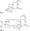
- Fig. 1 illustrates a generic example of a system including a LED device 20, which is usually composed of a series circuit of a plurality of LEDs (LED chain), and a LED driver circuit 10, to which the LED chain is connected.
- the LED driver circuit 20 may be implemented in one integrated circuit but may also be implemented using a combination of discrete circuit components and integrated circuits.
- the LED driver circuit 10 is configured to provide a load current iour to the LED device 20 and to control the load current i OUT so that its current value (at least approximately) matches a set-point (desired current value). It is understood that the system of Fig. 1 or similar systems may be used, for example, to produce a lighting module that includes the LED device 20 and all circuitry required to drive the LED device 20.
- the LED device 20 is connected between an output terminal OUT of the LED driver circuit 10 and a supply terminal PWR, to which an input voltage V IN is applied.
- the input voltage V EST may also be received at the terminal VIN of the LED driver circuit 10.
- the LED driver circuit 10 is connected to a ground terminal GND.
- the input voltage V IN may vary within a comparably wide range. In the present example, the input voltage may vary between 25 and 40 volts. However, this range may be different in other applications.
- the LED driver circuit 10 may be configured to operate the LED device 20 so that the electrical power (load current times input voltage) does not exceed a specific maximum power. In some applications the electrical power should not fall below a specific minimum power.
- the set-point is determined by the voltage V SET received at analog input terminal SET.
- the voltage V SET may be applied either using an external voltage source or by connecting a resistor R SET between the analog input terminal SET and, e.g., ground terminal GND.
- the current set-point used for the regulation of the load current may be proportional to the voltage V SET .
- a microcontroller may use analog-to-digital converters (included in common standard microcontrollers) to obtain measured values representing the input voltage V IN and the load current i OUT , wherein a digital-to-analog converter may be used to generate the desired voltage V SET , which may be adjusted, for example, dependent on an electrical power value calculated by the microcontroller based on the above-mentioned measured values.
- NVM non-volatile memory
- ISP wired in-system programming
- Fig. 2 illustrates a novel approach which may significantly improve flexibility while keeping the bill of materials and production costs low.
- the example of Fig. 2 includes a control circuit 5, an LED driver circuit 10 as well as an LED device 10 connected thereto.
- the LED driver circuit 10 and the LED device 20 are substantially the same as in the previous example of Fig. 1 and reference is made to the respective description above.
- a current sense resistor Rs is coupled in series to the LED device 20 in order to allow measurement of the load current.
- the resistor Rs is connected between the LED device 20 and the terminal PWR, at which the input voltage V EST is provided.
- the shunt resistor or other current sense circuitry may be integrated in the LED device 20 and the current information can be tapped at a dedicated sense terminal of the LED device 20.
- the control circuit 5 is configured to provide, at output terminal DOUT (digital output), an output voltage V PWM that is indicative of the set-point, which is used by the LED driver circuit for the purpose of output current regulation.
- the output voltage V PWM is a pulse-width modulated (PWM) signal that is converted to an analog voltage V SET using, for example, a low pass.
- PWM pulse-width modulated
- a simple R-C low-pass composed of one resistor R 1 and one capacitor C 1 may be sufficient to generate the voltage V SET from the PWM signal.
- the resistor R 1 and the capacitor C 1 may be integrated into the control circuit 5 or connected externally to an integrated circuit (IC).
- pulse-width modulation is merely one example and other types of modulation, such as sigma-delta modulation, may be employed instead.
- the low-pass may be regarded as an digital-to-analog converter that is configured to convert the (binary) PWM signal into the analog voltage V SET . It is understood that other approaches for digital-to-analog conversion may be used instead.
- the control circuit 5 has two analog inputs AIN1 and AIN2, which receive the input voltage V EST and the voltage Vs at the common circuit node of shunt resistor Rs and LED device 20.
- the voltage Vs equals V IN -R S ⁇ i OUT
- the control circuit 5 may include an analog-to-digital converter to digitize the voltages V IN and Vs; in this case the control circuit 5 can regularly digitally calculate the load current value and adjust the set-point in accordance with a given control characteristic.
- the set-point information is output as the PWM signal V PWM .
- the control circuit may include a Near Field Communication (NFC) transceiver circuit as well as an NFC antenna 4 connected thereto.
- NFC Near Field Communication
- the nominal set-point and other parameters can be easily programmed using an NFC coupling device (e.g. an NFC writer) that is configured to transmit the information about the parameters to the NFC transceiver circuit included in the control circuit 5, which then stores the received information, e.g., in a non-volatile memory (NVM) that may be integrated in the control circuit 5.
- NFC coupling device e.g. an NFC writer
- NVM non-volatile memory
- Fig. 3 illustrates one exemplary embodiment of the control circuit 5 used in the example of Fig. 2 .
- the control circuit 5 may be implemented in one single integrated circuit, e.g. an application specific integrated circuit (ASIC).
- the control circuit 5 includes a power management unit 50 (PMU), one or more analog-to-digital converters 52, the above-mentioned NFC transceiver 53, as well as a control logic 51, which basically forms a finite state machine (FSM).
- the control circuit 5 further includes an NVM 54, an arithmetic-logic unit 56 (ALU) and a modulator 55 configured to generate the PWM output signal V PMW (see Fig. 2 ).
- PMU power management unit 50
- ALU arithmetic-logic unit 56
- modulator 55 configured to generate the PWM output signal V PMW (see Fig. 2 ).
- An oscillator 57 generates a clock signal for the logic circuit 51, the ALU 56, the modulator 55 and further circuitry that need the clock signal for operation.
- the ALU 56 can be regarded as part of the logic circuit 51 which is, however, an implementation detail irrelevant for the function of the overall control circuit 5.
- the power management unit 50 receives, at respective supply pins, a first supply voltage Vcc (e.g. 5 volts) and a reference potential V GND , e.g. ground potential.
- Vcc a first supply voltage
- V GND a reference potential
- the PMU may receive a supply voltage V NFC from the NFC transceiver 53 when the NFC transceiver 53 receives energy from an external NFC coupling device (not shown) via NFC antenna 4.
- the NFC transceiver 53 and its functions will be discussed in more detail later.
- the PMU 50 is configured to provide voltage supply to all circuitry included in the control circuit 5.
- the analog-to-digital converter (ADC) 52 receives, at respective analog input pins (see Fig. 2 , terminals AIN1, AIN2), voltage signals V EST and Vs which carry information about the input voltage V IN and the load current i OUT passing through the LED device 20.
- ADC may have two channels that are able to simultaneously sample the voltage signals V IN and Vs or a multiplexer may be used to use one ADC channel for sampling both signals V IN and Vs in an alternating manner.
- the control logic 51 is configured to control the operation of the control circuit 5 and particularly the signal flow within the control circuit 5.
- the NVM 54 and the ALU 56 are connected to the control logic 51, which is configured to determine (with the help of the ALU 56) the set-point to be used for current regulation based on the parameters (e.g. the nominal set-point value) stored in the NVM 54 and the sampled values received from the ADC 52.
- the control logic 51 is further configured to provide the set-point information (e.g. in the form of a digital word) to the modulator 55.
- the modulator 55 is configured to output, e.g. at a digital output pin DOUT, a PWM signal V OUT which has a duty cycle that represents the set-point information.
- the control logic 51 will reduce the set-point accordingly and, consequently, the PWM signal output to the LED driver circuit 10 will indicate a lower set-point and the current regulator included in the LED driver circuit 10 will reduce the load current.
- the modulator 55 is not necessarily configured to perform pulse-width modulation (PWM), and other types of modulation such as, for example, sigma-delta modulation (pulse density modulation) are also applicable.
- parameters such as a nominal current set-point can be received by the NFC transceiver 53 from an external NFC coupling device (not shown in the figures) and stored in the NVM 54.
- the control circuit 5, and particularly the control logic 51 included therein is configured to operate in two different modes.
- the first mode which may be referred to as programming mode, is characterized in that the control circuit 5 is not supplied with the supply voltage Vcc at the respective supply pin but rather receives electrical power from an active NFC field generated by an external NFC device.
- the NFC transceiver will generate a supply voltage V NFC which can be distributed to the control logic 51 and the NVM 54 (e.g.
- the second mode which may be referred to as normal mode of operation, is characterized in that the control circuit 5 is supplied with the supply voltage Vcc at the respective supply pin.
- the NFC transceiver is disabled, e.g. by receiving a respective mode signal (disable signal) from the PMU 50 in response to the PMU 50 detecting the presence of the supply voltage VCC at the supply pin.
- the disable signal may be generated by the control logic 51 or other circuitry included in the control circuit 5.
- the NFC transceiver 53 being disabled means that the NFC transceiver 53 can neither generate an NFC field nor transmit any RF signals via the antenna 4.
- an electronic switch may be used to prevent the NFC transceiver 53 from generating the supply voltage V NFC from an externally generated (e.g. by an NFC coupling device) NFC field.
- the electronic switch e.g. a depletion MOS transistor
- the electronic switch may for example disconnect or short circuit a capacitor, which is used to buffer the voltage V NFC when the supply voltage Vcc is present at the respective supply pin.
- an electronic switch may be used, for example, to disconnect the NFC antenna 4 or otherwise disable the NFC antenna 4 (e.g. by short-circuiting the two antenna terminals using an electronic switch).
- the NFC transceiver 53 may be permanently deactivated once a parameter set has been successfully received via the NFC communication channel and stored in the NVM 54.
- This permanent deactivation may be achieved in various ways.
- the NFC transceiver may include an electrically programmable fuse bit which is set once a parameter set has been successfully received and stored. Based on the state of the fuse bit, the NFC transceiver 53 may be deactivated in a similar manner as described above.
- control logic 51 as well as the ALU 56 (which may also be regarded as part of the control logic 51) are composed of hard-wired circuit components and do not require software. In other words, the control logic 51 does not include a processor configured to execute software instructions. Furthermore, the control circuit 51, the PMU 50, the ADC 52 as well as the NFC transceiver 53 are integrated in a single chip or a single chip package. Integration in a common chip allows for a comparably simple deactivation of the NFC transceiver 53 when the supply voltage Vcc is received at the respective supply pin normal mode of operation).
- Fig. 4 is a flow chart illustrating a method in accordance with the invention. The method may be essentially (but not exclusively) performed by the control logic 51 of the control circuit 5 described above. According to Fig. 4 the circuit is able to operate in a first mode or a second mode. The circuit operates in the first mode, when a supply voltage Vcc is received at the supply pin ( Fig. 4 , step S1, yes-branch). The circuit operates in the second mode, when no supply voltage Vcc is received at the supply pin ( Fig. 4 , step S1, no-branch) and when an NFC field is present so that the NFC transceiver is able to generate an alternative supply voltage V NFC from the NFC field ( Fig. 4 , step S2, yes-branch).
- the circuit is passive and does not operate.
- the NFC transceiver is deactivated ( Fig. 4 , step S11). Further functions provided in the first mode (e.g. generating modulated signal V PWM , etc.) have been discussed above and not repeated here.
- the NFC field is the only source of energy of the circuit, and the NFC transceiver generates the alternative supply voltage V NFC for supplying other circuitry such as the control logic 51 and the NVM 54 (cf. Fig.
- the NFC communication channel Fig 4 , step S21
- the received data i.e. the one or more parameters discussed above, e.g. a nominal current set-point to be used for current regulation
- the NVM 54 Fig 4 , step S22
- operation in the second mode can only start when the fuse bit state indicates that the NVM 54 has not yet been programmed. Once the fuse bit has been fused (set) the NFC transceiver 53 is prevented from generating the alternative supply voltage V NFC from an external NFC field, and thus the circuit does not power up.
Landscapes
- Engineering & Computer Science (AREA)
- Computer Networks & Wireless Communication (AREA)
- Signal Processing (AREA)
- Power Engineering (AREA)
- Circuit Arrangement For Electric Light Sources In General (AREA)
Description
- The present disclosure relates to controllers for use in lighting applications, particularly in lighting applications using LED devices.
- LEDs (Light Emitting Diodes) are usually operated using a controlled load current. The load current control is usually implemented using dedicated LED driver circuits which may be configured to regulate the load current passing through a LED module (usually a series circuit of a plurality of LEDs) to match a given set-point. The set-point may be configurable. For example, the set-point may be set in accordance with an analog input voltage, which represents the information about the desired set-point (and thus about the desired output power). In low-cost applications, the set-point may be set using a resistor supplied with a constant current so that the voltage that determines the set-point is substantially proportional to the resistance of the resistor. In some applications DIP switches are used to select resistors of a resistor network, thereby adjusting the effective resistance of the resistor network which determines the mentioned set-point.
- In applications in which the input voltage (supply voltage) can vary within a comparably wide range (e.g. 25 to 40 volts), a power limitation may be included in the LED driver circuit to ensure that the electrical power provided to the LED device does not exceed a maximum value. Similarly, the electrical power provided to the LED device should not fall below a minimum value. These power limits may also be configurable in order to comply with the requirements of a specific application. In some applications simple but expensive discrete analog circuitry is used to implement the above-mentioned power limitation.
- In more sophisticated (with regard to flexibility) applications, a microcontroller may be used in connection with a LED driver circuit, wherein the microcontroller may be programmed to sense voltage and load current (using an analog-to-digital converter) and to control the above-mentioned set-point in order to operate the LED device within specified limits. Such a solution provides some improved flexibility, but still has some deficits with regard to handling, since the application-dependent and customer-dependent configuration parameters (e.g. nominal current set-point, power limit, etc.) need to be written into a non-volatile memory of the microcontroller at the end of the manufacturing process.
- Reference is made to the
publications DE 10 2015 105 466 A1 ,WO 2016/081244 A1 ,US 2013/0234658 A1 ,CN 106298960 A ,US 2014/0120832 A1 , andWO 2018/010687 A1 . Thepublication DE 10 2015 105 466 A1 relates to a driver circuit for LED devices used in illumination products. The driver circuit includes a wireless interface for receiving information relating to the operation of the illumination product. The publicationWO 2016/081244 A1 relates to a medical device which can be activated by bringing an NFC enabled mobile device into close proximity of the medical device, thus making a dedicated witch dispensable. The publicationUS 2013/0234658 A1 relates to a wireless charging circuit. - According to the invention a circuit comprises a supply pin configured to receive a supply voltage, a non-volatile memory for storing one or more parameters, and a Near Field Communication (NFC) transceiver that is configured to receive data representing the one or more parameters in a second mode of operation, in which no supply voltage is received at the supply pin . The circuit is configured in a first mode of operation to deactivate the NFC transceiver in response to receiving the supply voltage at the supply pin The circuit comprises a modulator configured to generate, in the first mode of operation, a modulated output signal, which depends on at least one of the one or more parameters stored in the non-volatile memory.
- Further, a method for operating a circuit, which comprises a supply pin, a non-volatile memory, and a NFC transceiver, is described herein according to the invention. The method comprises - in a second mode of operation, in which no supply voltage is received at the supply pin - receiving, by the NFC transceiver, data representing one or more parameters and storing the one or more parameters in the non-volatile memory, and - in a first mode of operation, in which the supply voltage is received at the supply pin - deactivating the NFC transceiver The method further comprises, in the first mode of operation, generating a modulated output signal dependent on at least one of the one or more parameters stored in the non-volatile memory
- The invention can be better understood with reference to the following drawings and descriptions. The components in the figures are not necessarily to scale; instead emphasis is placed upon illustrating the principles of the invention. Moreover, in the figures, like reference numerals designate corresponding parts. In the drawings:
-
Figure 1 illustrates a generic example of an LED device connected to a driver circuit. -
Figure 2 illustrates one example of an application of an integrated control circuit with an integrated NFC module for the purpose of controlling an LED driver circuit connected to an LED device. -
Figure 3 illustrates one embodiment of the control circuit used in the example ofFig. 2 -
Figure 4 is a flow chart illustrating a method for operating a control circuit in accordance with one embodiment. -
Fig. 1 illustrates a generic example of a system including aLED device 20, which is usually composed of a series circuit of a plurality of LEDs (LED chain), and aLED driver circuit 10, to which the LED chain is connected. TheLED driver circuit 20 may be implemented in one integrated circuit but may also be implemented using a combination of discrete circuit components and integrated circuits. Generally, theLED driver circuit 10 is configured to provide a load current iour to theLED device 20 and to control the load current iOUT so that its current value (at least approximately) matches a set-point (desired current value). It is understood that the system ofFig. 1 or similar systems may be used, for example, to produce a lighting module that includes theLED device 20 and all circuitry required to drive theLED device 20. - In the example of
Fig. 1 theLED device 20 is connected between an output terminal OUT of theLED driver circuit 10 and a supply terminal PWR, to which an input voltage VIN is applied. The input voltage VEST may also be received at the terminal VIN of theLED driver circuit 10. Further, theLED driver circuit 10 is connected to a ground terminal GND. The input voltage VIN may vary within a comparably wide range. In the present example, the input voltage may vary between 25 and 40 volts. However, this range may be different in other applications. As the luminous flux generated by a LED basically depends on the load current passing through the LED, the load current needs to be regulated in accordance with a set-point as mentioned above. Further, theLED driver circuit 10 may be configured to operate theLED device 20 so that the electrical power (load current times input voltage) does not exceed a specific maximum power. In some applications the electrical power should not fall below a specific minimum power. - Particularly when using an integrated driver circuit, the customer/user needs to have the possibility to set the mentioned set-point that is used for load current regulation. In the example of
Fig. 1 the set-point is determined by the voltage VSET received at analog input terminal SET. The voltage VSET may be applied either using an external voltage source or by connecting a resistor RSET between the analog input terminal SET and, e.g., ground terminal GND. In this case, the LED driver circuit may be configured to provide a defined constant current iSET at the terminal SET, thereby causing a voltage VSET = iSET·RSET across the resistor RSET (wherein RSET also refers to the resistance of the respective resistor). The current set-point used for the regulation of the load current may be proportional to the voltage VSET. - Using a discrete resistor RSET connected to an integrated LED driver circuit allows configuration of the mentioned set-point used for current regulation. However, such a solution increases the bill of material and, even more important, provides little flexibility as
different LED devices 20 will usually require different resistors for selecting different set-points. If further parameters (in addition to the set-point) such as the above-mentioned maximum power are to be selected using external components, the complexity and related costs will increase even further. - Another known approach consists in the use of a programmable microcontroller for generating the voltage VSET, which determines the set-point for load current regulation. A microcontroller may use analog-to-digital converters (included in common standard microcontrollers) to obtain measured values representing the input voltage VIN and the load current iOUT, wherein a digital-to-analog converter may be used to generate the desired voltage VSET, which may be adjusted, for example, dependent on an electrical power value calculated by the microcontroller based on the above-mentioned measured values. Although using microcontrollers may somewhat improve flexibility, there is still the need to set the load current set-point, e.g. by programming it into a non-volatile memory (NVM) of the microcontroller, e.g. using a wired in-system programming (ISP) interface at the end of production of each individual product. Furthermore, the approach of using a microcontroller entails significant costs for a microcontroller which will, in most cases, have a performance capability that is far too high for an application as simple as the present one.
-
Fig. 2 illustrates a novel approach which may significantly improve flexibility while keeping the bill of materials and production costs low. The example ofFig. 2 includes acontrol circuit 5, anLED driver circuit 10 as well as anLED device 10 connected thereto. TheLED driver circuit 10 and theLED device 20 are substantially the same as in the previous example ofFig. 1 and reference is made to the respective description above. Different fromFig. 1 , a current sense resistor Rs is coupled in series to theLED device 20 in order to allow measurement of the load current. In the present example, the resistor Rs is connected between theLED device 20 and the terminal PWR, at which the input voltage VEST is provided. It is understood that other approaches for current sensing may be used instead. In other embodiments the shunt resistor or other current sense circuitry may be integrated in theLED device 20 and the current information can be tapped at a dedicated sense terminal of theLED device 20. - The
control circuit 5 is configured to provide, at output terminal DOUT (digital output), an output voltage VPWM that is indicative of the set-point, which is used by the LED driver circuit for the purpose of output current regulation. In the present example, the output voltage VPWM is a pulse-width modulated (PWM) signal that is converted to an analog voltage VSET using, for example, a low pass. Dependent on the application, a simple R-C low-pass composed of one resistor R1 and one capacitor C1 may be sufficient to generate the voltage VSET from the PWM signal. The resistor R1 and the capacitor C1 may be integrated into thecontrol circuit 5 or connected externally to an integrated circuit (IC). It is understood that pulse-width modulation is merely one example and other types of modulation, such as sigma-delta modulation, may be employed instead. In essence, the low-pass may be regarded as an digital-to-analog converter that is configured to convert the (binary) PWM signal into the analog voltage VSET. It is understood that other approaches for digital-to-analog conversion may be used instead. - In the present example, the
control circuit 5 has two analog inputs AIN1 and AIN2, which receive the input voltage VEST and the voltage Vs at the common circuit node of shunt resistor Rs andLED device 20. In this example, the voltage Vs equals VIN-RS·iOUT, and the control circuit can determine the load current according to the equation iOUT=(VIN-VS)/RS. Thecontrol circuit 5 may include an analog-to-digital converter to digitize the voltages VIN and Vs; in this case thecontrol circuit 5 can regularly digitally calculate the load current value and adjust the set-point in accordance with a given control characteristic. As mentioned, in the present example the set-point information is output as the PWM signal VPWM. - In order to make the programming of parameters such as the nominal set-point used for load current regulation easier and more flexible, the control circuit may include a Near Field Communication (NFC) transceiver circuit as well as an
NFC antenna 4 connected thereto. At the end of production (or at any time during the production process of the control circuit or the lighting module), the nominal set-point and other parameters can be easily programmed using an NFC coupling device (e.g. an NFC writer) that is configured to transmit the information about the parameters to the NFC transceiver circuit included in thecontrol circuit 5, which then stores the received information, e.g., in a non-volatile memory (NVM) that may be integrated in thecontrol circuit 5. It is understood that the mentioned nominal set-point and other parameters are customer or application specific and chosen for a specific application, e.g. a specific lighting module with a specific LED device. -
Fig. 3 illustrates one exemplary embodiment of thecontrol circuit 5 used in the example ofFig. 2 . Thecontrol circuit 5 may be implemented in one single integrated circuit, e.g. an application specific integrated circuit (ASIC). According toFig. 3 , thecontrol circuit 5 includes a power management unit 50 (PMU), one or more analog-to-digital converters 52, the above-mentionedNFC transceiver 53, as well as acontrol logic 51, which basically forms a finite state machine (FSM). Thecontrol circuit 5 further includes anNVM 54, an arithmetic-logic unit 56 (ALU) and amodulator 55 configured to generate the PWM output signal VPMW (seeFig. 2 ). Anoscillator 57 generates a clock signal for thelogic circuit 51, the ALU 56, themodulator 55 and further circuitry that need the clock signal for operation. As illustrated inFig. 3 , the ALU 56 can be regarded as part of thelogic circuit 51 which is, however, an implementation detail irrelevant for the function of theoverall control circuit 5. - The
power management unit 50 receives, at respective supply pins, a first supply voltage Vcc (e.g. 5 volts) and a reference potential VGND, e.g. ground potential. Alternatively to the supply voltage Vcc, the PMU may receive a supply voltage VNFC from theNFC transceiver 53 when theNFC transceiver 53 receives energy from an external NFC coupling device (not shown) viaNFC antenna 4. However, theNFC transceiver 53 and its functions will be discussed in more detail later. Although not all supply lines are explicitly shown inFig. 3 , thePMU 50 is configured to provide voltage supply to all circuitry included in thecontrol circuit 5. - The analog-to-digital converter (ADC) 52 receives, at respective analog input pins (see
Fig. 2 , terminals AIN1, AIN2), voltage signals VEST and Vs which carry information about the input voltage VIN and the load current iOUT passing through theLED device 20. Various options for sensing the load current have already been discussed above with reference toFig. 2 and are thus not repeated here. The ADC may have two channels that are able to simultaneously sample the voltage signals VIN and Vs or a multiplexer may be used to use one ADC channel for sampling both signals VIN and Vs in an alternating manner. - The
control logic 51 is configured to control the operation of thecontrol circuit 5 and particularly the signal flow within thecontrol circuit 5. TheNVM 54 and the ALU 56 are connected to thecontrol logic 51, which is configured to determine (with the help of the ALU 56) the set-point to be used for current regulation based on the parameters (e.g. the nominal set-point value) stored in theNVM 54 and the sampled values received from theADC 52. Thecontrol logic 51 is further configured to provide the set-point information (e.g. in the form of a digital word) to themodulator 55. Themodulator 55 is configured to output, e.g. at a digital output pin DOUT, a PWM signal VOUT which has a duty cycle that represents the set-point information. If, for example, the input voltage VIN increases to such an extent that the total electrical power (input voltage VIN times load current iOUT, seeFig. 2 ) exceeds a specific maximum value, then thecontrol logic 51 will reduce the set-point accordingly and, consequently, the PWM signal output to theLED driver circuit 10 will indicate a lower set-point and the current regulator included in theLED driver circuit 10 will reduce the load current. As already mentioned above, themodulator 55 is not necessarily configured to perform pulse-width modulation (PWM), and other types of modulation such as, for example, sigma-delta modulation (pulse density modulation) are also applicable. - As mentioned, parameters such as a nominal current set-point can be received by the
NFC transceiver 53 from an external NFC coupling device (not shown in the figures) and stored in theNVM 54. In one embodiment thecontrol circuit 5, and particularly thecontrol logic 51 included therein, is configured to operate in two different modes. The first mode, which may be referred to as programming mode, is characterized in that thecontrol circuit 5 is not supplied with the supply voltage Vcc at the respective supply pin but rather receives electrical power from an active NFC field generated by an external NFC device. In this first mode, the NFC transceiver will generate a supply voltage VNFC which can be distributed to thecontrol logic 51 and the NVM 54 (e.g. via the PMU 50) in order to allow storing the parameters received from the NFC coupling device via the NFC communication channel in theNVM 54. The second mode, which may be referred to as normal mode of operation, is characterized in that thecontrol circuit 5 is supplied with the supply voltage Vcc at the respective supply pin. In the second mode, the NFC transceiver is disabled, e.g. by receiving a respective mode signal (disable signal) from thePMU 50 in response to thePMU 50 detecting the presence of the supply voltage VCC at the supply pin. Alternatively, the disable signal may be generated by thecontrol logic 51 or other circuitry included in thecontrol circuit 5. TheNFC transceiver 53 being disabled means that theNFC transceiver 53 can neither generate an NFC field nor transmit any RF signals via theantenna 4. - Disabling the
NFC transceiver 53 may be achieved in various ways. For example, an electronic switch may be used to prevent theNFC transceiver 53 from generating the supply voltage VNFC from an externally generated (e.g. by an NFC coupling device) NFC field. The electronic switch (e.g. a depletion MOS transistor), may for example disconnect or short circuit a capacitor, which is used to buffer the voltage VNFC when the supply voltage Vcc is present at the respective supply pin. Alternatively, an electronic switch may be used, for example, to disconnect theNFC antenna 4 or otherwise disable the NFC antenna 4 (e.g. by short-circuiting the two antenna terminals using an electronic switch). - In one specific embodiment, the
NFC transceiver 53 may be permanently deactivated once a parameter set has been successfully received via the NFC communication channel and stored in theNVM 54. This permanent deactivation may be achieved in various ways. For example, the NFC transceiver may include an electrically programmable fuse bit which is set once a parameter set has been successfully received and stored. Based on the state of the fuse bit, theNFC transceiver 53 may be deactivated in a similar manner as described above. - Ensuring that the NFC transceiver is inactive during the normal mode of operation, i.e. when the
control circuit 5 is supplied with the supply voltage Vcc, has the advantage that the chip including thecontrol circuit 5 will not be regarded as an RF device in various legislations. As a consequence, certification of the RF device will not be required in these legislations. Furthermore, it can be ensured that the RF circuits included in the NFC transceivers will not cause any electromagnetic interferences (EMI) and related disturbances in other electronic components or devices. - It should be noted that the
control logic 51 as well as the ALU 56 (which may also be regarded as part of the control logic 51) are composed of hard-wired circuit components and do not require software. In other words, thecontrol logic 51 does not include a processor configured to execute software instructions. Furthermore, thecontrol circuit 51, thePMU 50, theADC 52 as well as theNFC transceiver 53 are integrated in a single chip or a single chip package. Integration in a common chip allows for a comparably simple deactivation of theNFC transceiver 53 when the supply voltage Vcc is received at the respective supply pin normal mode of operation). -
Fig. 4 is a flow chart illustrating a method in accordance with the invention. The method may be essentially (but not exclusively) performed by thecontrol logic 51 of thecontrol circuit 5 described above. According toFig. 4 the circuit is able to operate in a first mode or a second mode. The circuit operates in the first mode, when a supply voltage Vcc is received at the supply pin (Fig. 4 , step S1, yes-branch). The circuit operates in the second mode, when no supply voltage Vcc is received at the supply pin (Fig. 4 , step S1, no-branch) and when an NFC field is present so that the NFC transceiver is able to generate an alternative supply voltage VNFC from the NFC field (Fig. 4 , step S2, yes-branch). If neither a supply voltage Vcc is received nor an NFC field is present, then the circuit is passive and does not operate. In the first mode of operation, it is ensured that the NFC transceiver is deactivated (Fig. 4 , step S11). Further functions provided in the first mode (e.g. generating modulated signal VPWM, etc.) have been discussed above and not repeated here. In the second mode of operation, the NFC field is the only source of energy of the circuit, and the NFC transceiver generates the alternative supply voltage VNFC for supplying other circuitry such as thecontrol logic 51 and the NVM 54 (cf.Fig. 3 ), so that data can be received via the NFC communication channel (Fig 4 , step S21) and the received data (i.e. the one or more parameters discussed above, e.g. a nominal current set-point to be used for current regulation) can be stored in the NVM 54 (Fig 4 , step S22). In one specific embodiment, which makes use of the fuse bit circuit mentioned above, operation in the second mode can only start when the fuse bit state indicates that theNVM 54 has not yet been programmed. Once the fuse bit has been fused (set) theNFC transceiver 53 is prevented from generating the alternative supply voltage VNFC from an external NFC field, and thus the circuit does not power up. - Although the invention has been illustrated and described with respect to one or more implementations, alterations and/or modifications may be made to the illustrated examples without departing from the scope of the appended claims.
Claims (13)
- A circuit comprising:a supply pin configured to receive a supply voltage (Vcc);a non-volatile memory (54) for storing one or more parameters;a Near Field Communication, NFC, transceiver (53) which is configured to receive data representing the one or more parameters in a second mode of operation, in which no supply voltage (Vcc) is received at the supply pin ;wherein the circuit is configured in a first mode of operation to deactivate the NFC transceiver (53) in response to receiving the supply voltage (Vcc) at the supply pin,characterized in that the circuit comprises a modulator (55) configured to generate, in the first mode of operation, a modulated output signal (VPwM), which depends on at least one of the one or more parameters stored in the non-volatile memory.
- The circuit of claim 1, further comprising:
an analog-to-digital converter (52) configured to receive and digitize a first signal (VIN) and a second signal (Vs); - The circuit of claim 2, further comprising:
a modulator (55) configured to generate a modulated output signal (VPWM), which depends on at least one of the one or more parameters stored in the non-volatile memory (54) as well as on the first signal (VIN) and the second signal (Vs). - The circuit of any of claims 1 to 3, further comprising:
a control logic (51) configured to operate:in a first mode, when the supply voltage (Vcc) is received at the supply pin, andin a second mode, when no supply voltage (Vcc) is received at the supply pin and a further supply voltage (VNFC) is generated by the NFC transceiver (53). - The circuit of claim 4,
wherein the NFC transceiver (53) is operably coupled to an NFC antenna (4) and configured to generate the further supply voltage (VNFC) from an active NFC field received by the NFC antenna (4). - The circuit of claim 4, if dependent on claim 3,
wherein the first signal (VIN) is indicative of a voltage provided to a load and the second signal (Vs) is indicative of a load current (iOUT) passing through the load;
wherein the control logic (51) is configured to determine a value indicative of the electric power from the digitized first signal (VIN) and the digitized second signal (Vs); and
wherein, in the first mode, the modulated output signal (VPWM) has a duty cycle depending on at least one of the one or more parameters stored in the non-volatile memory (54) and the determined value indicative of the electric power. - The circuit of any of claims 1 to 6, further comprising:
a power management unit, PMU, (50) coupled to the supply pin and configured to detect, whether, or not, the supply voltage (Vcc) is received at the supply pin. - The circuit of claim 7,
wherein the PMU (50) is further configured to generate a signal (MODE) that causes the NFC transceiver (53) to be deactivated when the PMU (50) detects that the supply voltage (Vcc) is not received at the supply pin. - The circuit claim 4 further comprising:a fuse bit circuit,wherein the circuit is configured to deactivate the NFC transceiver (53) in response to the state of the fuse bit circuit; the state of the fuse bit circuit being indicative of whether, or not, the one or more parameters have been previously stored in the non-volatile memory (54) while operating in the second mode.
- A system including:a lighting device (20) including at least one light emitting diode;a driver circuit (10) connected to the lighting device (20) and configured to provide a load current (iOUT) to the lighting device (20) that is regulated in accordance with a set-point value, which is determined by a set signal (VSET) received at an input pin (SET) of the driver circuit (10);a circuit (5) according to any of claims 1 to 3,wherein the modulated output signal (VPWM) is indicative of the set-point value and wherein the set signal (VSET) is determined by the modulated output signal (VPWM).
- The system of claim 10, further comprising:
a low-pass filter (R1, C1) coupled between the circuit (5) and the driver circuit (10) and configured to receive the modulated output signal (VPWM) and to generate therefrom the set signal (VSET). - A method for operating a circuit, which comprises a supply pin, a non-volatile memory (54), and a Near Field Communication (NFC) transceiver (53), the method comprising:in a second mode of operation, in which no supply voltage (Vcc) is received at the supply pin: receiving, by the NFC transceiver (53), data representing one or more parameters and storing the one or more parameters in the non-volatile memory;in a first mode of operation, in which the supply voltage (Vcc) is received at the supply pin: deactivating the NFC transceiver (53),
characterized in that
the method further comprises, in the first mode of operation, generating a modulated output signal (VPWM) dependent on at least one of the one or more parameters stored in the non-volatile memory. - The method of claim 12,
wherein the modulated output signal (VPWM) represents a current set-point used by a current regulator of a LED driver (10), which provides a regulated output current to a LED device (20).
Priority Applications (3)
| Application Number | Priority Date | Filing Date | Title |
|---|---|---|---|
| EP19166553.8A EP3719994B1 (en) | 2019-04-01 | 2019-04-01 | Power regulation for lighting using nfc |
| US16/830,751 US11394428B2 (en) | 2019-04-01 | 2020-03-26 | Power regulation for lighting using NFC |
| CN202010235954.6A CN111800913B (en) | 2019-04-01 | 2020-03-30 | Control circuit, system for lighting and method for operating a circuit |
Applications Claiming Priority (1)
| Application Number | Priority Date | Filing Date | Title |
|---|---|---|---|
| EP19166553.8A EP3719994B1 (en) | 2019-04-01 | 2019-04-01 | Power regulation for lighting using nfc |
Publications (2)
| Publication Number | Publication Date |
|---|---|
| EP3719994A1 EP3719994A1 (en) | 2020-10-07 |
| EP3719994B1 true EP3719994B1 (en) | 2021-05-26 |
Family
ID=66049074
Family Applications (1)
| Application Number | Title | Priority Date | Filing Date |
|---|---|---|---|
| EP19166553.8A Active EP3719994B1 (en) | 2019-04-01 | 2019-04-01 | Power regulation for lighting using nfc |
Country Status (3)
| Country | Link |
|---|---|
| US (1) | US11394428B2 (en) |
| EP (1) | EP3719994B1 (en) |
| CN (1) | CN111800913B (en) |
Families Citing this family (1)
| Publication number | Priority date | Publication date | Assignee | Title |
|---|---|---|---|---|
| EP4072246A1 (en) * | 2021-04-06 | 2022-10-12 | Tridonic GmbH & Co. KG | Operating device for lighting means |
Family Cites Families (37)
| Publication number | Priority date | Publication date | Assignee | Title |
|---|---|---|---|---|
| JPH07192925A (en) | 1993-12-27 | 1995-07-28 | Taiyo Yuden Co Ltd | Bead inductor |
| TW553465U (en) | 2002-07-25 | 2003-09-11 | Micro Star Int Co Ltd | Integrated inductor |
| US7646028B2 (en) * | 2003-06-17 | 2010-01-12 | Semiconductor Components Industries, L.L.C. | LED driver with integrated bias and dimming control storage |
| CN101189623B (en) * | 2003-10-29 | 2010-06-02 | Nxp股份有限公司 | Communication partner appliance with automatic send mode activation and the method |
| CN101053185A (en) * | 2004-10-29 | 2007-10-10 | 菲尼萨公司 | Transceiver based on loop back initiation |
| US20110062888A1 (en) * | 2004-12-01 | 2011-03-17 | Bondy Montgomery C | Energy saving extra-low voltage dimmer and security lighting system wherein fixture control is local to the illuminated area |
| US8169185B2 (en) * | 2006-01-31 | 2012-05-01 | Mojo Mobility, Inc. | System and method for inductive charging of portable devices |
| JP4685128B2 (en) | 2007-06-08 | 2011-05-18 | Necトーキン株式会社 | Inductor |
| KR20110003725A (en) * | 2009-07-06 | 2011-01-13 | 삼성전자주식회사 | Transceiver for controlling the swing width of output voltage, method for controlling the swing width of output voltage |
| KR101583093B1 (en) * | 2010-07-08 | 2016-01-07 | 주식회사 케이티 | Method for supporting different types of UICC cards and Terminal therefor |
| JP2012019431A (en) * | 2010-07-09 | 2012-01-26 | Sumitomo Electric Ind Ltd | Optical data link |
| JP5744004B2 (en) * | 2010-07-23 | 2015-07-01 | パナソニック インテレクチュアル プロパティ コーポレーション オブアメリカPanasonic Intellectual Property Corporation of America | NFC communication apparatus and control method thereof |
| JP2012104555A (en) | 2010-11-08 | 2012-05-31 | Kitagawa Ind Co Ltd | Ferrite core and choke |
| US8482225B2 (en) * | 2011-04-28 | 2013-07-09 | Allegro Microsystems, Llc | Electronic circuits and methods for driving a diode load |
| TWI423279B (en) | 2011-07-05 | 2014-01-11 | Delta Electronics Inc | Inductor assembly |
| US8729815B2 (en) * | 2012-03-12 | 2014-05-20 | Osram Sylvania Inc. | Current control system |
| JP2013191913A (en) * | 2012-03-12 | 2013-09-26 | Renesas Electronics Corp | Wireless charging circuit, wireless charging system, and semiconductor device |
| US9042826B2 (en) * | 2012-10-25 | 2015-05-26 | Samsung Electronics Co., Ltd. | Apparatus and method for power state transition via near field communication |
| TWI492660B (en) * | 2013-01-10 | 2015-07-11 | 碩頡科技股份有限公司 | Light emitting diode load driving apparatus |
| US9687930B2 (en) * | 2013-03-15 | 2017-06-27 | Lincoln Global, Inc. | Systems and methods for networking, configuration, calibration and identification of welding equipment |
| WO2015006810A1 (en) * | 2013-07-17 | 2015-01-22 | Malcolm Douglass | A residential management system |
| PT3036976T (en) * | 2013-08-19 | 2020-01-20 | Signify Holding Bv | Programmable lighting device and method and system for programming lighting device |
| SG2013074323A (en) * | 2013-10-03 | 2015-05-28 | Schneider Electric South East Asia Hq Pte Ltd | A switching device and a method of controlling the same |
| US9928672B2 (en) * | 2013-12-05 | 2018-03-27 | Wallflower Labs Inc. | System and method of monitoring and controlling appliances and powered devices using radio-enabled proximity sensing |
| WO2015104936A1 (en) | 2014-01-07 | 2015-07-16 | 株式会社村田製作所 | Ferrite core and noise filter |
| US20150296598A1 (en) * | 2014-04-11 | 2015-10-15 | Infineon Technologies Ag | Contactless Device Configuration |
| US9851772B2 (en) * | 2014-08-22 | 2017-12-26 | Linear Technology Corporation | 1-wire bus PD detection and classification scheme for ethernet PoDL |
| CA2965658A1 (en) * | 2014-11-18 | 2016-05-26 | Mc10, Inc. | System, device, and method for electronic device activation |
| US20170178797A1 (en) | 2015-12-21 | 2017-06-22 | Infineon Technologies Austria Ag | Surface Mount Inductor for Placement Over a Power Stage of a Power Converter |
| CN106025497B (en) * | 2016-07-14 | 2019-08-06 | 浙江生辉照明有限公司 | FM antenna, NFC antenna, Multi-Function Antenna and lighting apparatus |
| TW201814928A (en) * | 2016-09-26 | 2018-04-16 | 友達光電股份有限公司 | Near field communication sensor device |
| DE102017106896B4 (en) * | 2017-03-30 | 2023-02-02 | Infineon Technologies Ag | Electronic switch for electronic fuse |
| CN107731441A (en) | 2017-10-19 | 2018-02-23 | 杭州华为数字技术有限公司 | The assembly method of magnetic element and magnetic element |
| FR3078423B1 (en) * | 2018-02-27 | 2020-09-04 | St Microelectronics Grenoble 2 | RFID CONTROL INTERFACE |
| FR3078451A1 (en) * | 2018-02-27 | 2019-08-30 | Stmicroelectronics (Grenoble 2) Sas | POWER VARIATION CONTROL SYSTEM |
| FR3078424B1 (en) * | 2018-02-27 | 2021-04-09 | St Microelectronics Grenoble 2 | GENERATION OF A PWM SIGNAL |
| CN109920620B (en) | 2019-03-28 | 2024-03-29 | 罗山县三通达电子科技有限公司 | Common mode choke coil for eliminating electrostatic interference |
-
2019
- 2019-04-01 EP EP19166553.8A patent/EP3719994B1/en active Active
-
2020
- 2020-03-26 US US16/830,751 patent/US11394428B2/en active Active
- 2020-03-30 CN CN202010235954.6A patent/CN111800913B/en active Active
Also Published As
| Publication number | Publication date |
|---|---|
| US20200313727A1 (en) | 2020-10-01 |
| EP3719994A1 (en) | 2020-10-07 |
| CN111800913A (en) | 2020-10-20 |
| CN111800913B (en) | 2024-02-13 |
| US11394428B2 (en) | 2022-07-19 |
Similar Documents
| Publication | Publication Date | Title |
|---|---|---|
| EP3276808B1 (en) | Accurate non-isolated high voltage dc-dc feedback | |
| US9131577B2 (en) | Light emitting element drive device | |
| US10728993B2 (en) | Driver circuit for providing constant voltage to an auxiliary circuit | |
| US9544970B2 (en) | Detection of an LED module | |
| KR20020093031A (en) | Dual mode pulse-width modulator for power control applications | |
| WO2013102879A1 (en) | Power converter with separate buck and boost conversion circuits | |
| US11737180B2 (en) | Control circuit, chip and control method | |
| US9603205B2 (en) | Multi-function terminal configurable to implement two functionalities | |
| US10568174B1 (en) | Apparatus and methods for controlling LED light flux | |
| CN106572554B (en) | With the electronic controller to Unknown worm and the automatic adjustment of load voltage | |
| EP3719994B1 (en) | Power regulation for lighting using nfc | |
| US20160098046A1 (en) | Configurable led power supply with wireless interface | |
| CN103580491B (en) | There is the configurable power controller of combinatorial input | |
| EP3095301B1 (en) | A circuit arrangement for operating led strings | |
| US10356873B1 (en) | Multiple interface LED driver with inherent overvoltage protection | |
| US20220376699A1 (en) | Inductive current digital-to-analog converter (dac) and related control options | |
| CN111132411B (en) | Semiconductor device for outputting control parameter and light emitting apparatus | |
| JP7486517B2 (en) | Power delivery configuration across the isolation barrier | |
| US9577521B2 (en) | Average current control for a switched power converter | |
| US20100188015A1 (en) | Method and apparatus for controlling and modulating led current | |
| CN101727079B (en) | Integrated circuit and operation mode determining method | |
| TWI569581B (en) | Auto-adjustable pulse width modulation signal generator | |
| CN115209590A (en) | Operating device for a lighting device |
Legal Events
| Date | Code | Title | Description |
|---|---|---|---|
| PUAI | Public reference made under article 153(3) epc to a published international application that has entered the european phase |
Free format text: ORIGINAL CODE: 0009012 |
|
| STAA | Information on the status of an ep patent application or granted ep patent |
Free format text: STATUS: REQUEST FOR EXAMINATION WAS MADE |
|
| 17P | Request for examination filed |
Effective date: 20200217 |
|
| AK | Designated contracting states |
Kind code of ref document: A1 Designated state(s): AL AT BE BG CH CY CZ DE DK EE ES FI FR GB GR HR HU IE IS IT LI LT LU LV MC MK MT NL NO PL PT RO RS SE SI SK SM TR |
|
| AX | Request for extension of the european patent |
Extension state: BA ME |
|
| GRAP | Despatch of communication of intention to grant a patent |
Free format text: ORIGINAL CODE: EPIDOSNIGR1 |
|
| STAA | Information on the status of an ep patent application or granted ep patent |
Free format text: STATUS: GRANT OF PATENT IS INTENDED |
|
| INTG | Intention to grant announced |
Effective date: 20201113 |
|
| GRAS | Grant fee paid |
Free format text: ORIGINAL CODE: EPIDOSNIGR3 |
|
| GRAA | (expected) grant |
Free format text: ORIGINAL CODE: 0009210 |
|
| STAA | Information on the status of an ep patent application or granted ep patent |
Free format text: STATUS: THE PATENT HAS BEEN GRANTED |
|
| AK | Designated contracting states |
Kind code of ref document: B1 Designated state(s): AL AT BE BG CH CY CZ DE DK EE ES FI FR GB GR HR HU IE IS IT LI LT LU LV MC MK MT NL NO PL PT RO RS SE SI SK SM TR |
|
| REG | Reference to a national code |
Ref country code: GB Ref legal event code: FG4D |
|
| REG | Reference to a national code |
Ref country code: CH Ref legal event code: EP |
|
| REG | Reference to a national code |
Ref country code: DE Ref legal event code: R096 Ref document number: 602019004801 Country of ref document: DE |
|
| REG | Reference to a national code |
Ref country code: AT Ref legal event code: REF Ref document number: 1397262 Country of ref document: AT Kind code of ref document: T Effective date: 20210615 |
|
| REG | Reference to a national code |
Ref country code: IE Ref legal event code: FG4D |
|
| REG | Reference to a national code |
Ref country code: NL Ref legal event code: FP |
|
| REG | Reference to a national code |
Ref country code: LT Ref legal event code: MG9D |
|
| PG25 | Lapsed in a contracting state [announced via postgrant information from national office to epo] |
Ref country code: BG Free format text: LAPSE BECAUSE OF FAILURE TO SUBMIT A TRANSLATION OF THE DESCRIPTION OR TO PAY THE FEE WITHIN THE PRESCRIBED TIME-LIMIT Effective date: 20210826 Ref country code: FI Free format text: LAPSE BECAUSE OF FAILURE TO SUBMIT A TRANSLATION OF THE DESCRIPTION OR TO PAY THE FEE WITHIN THE PRESCRIBED TIME-LIMIT Effective date: 20210526 Ref country code: HR Free format text: LAPSE BECAUSE OF FAILURE TO SUBMIT A TRANSLATION OF THE DESCRIPTION OR TO PAY THE FEE WITHIN THE PRESCRIBED TIME-LIMIT Effective date: 20210526 Ref country code: LT Free format text: LAPSE BECAUSE OF FAILURE TO SUBMIT A TRANSLATION OF THE DESCRIPTION OR TO PAY THE FEE WITHIN THE PRESCRIBED TIME-LIMIT Effective date: 20210526 |
|
| PG25 | Lapsed in a contracting state [announced via postgrant information from national office to epo] |
Ref country code: GR Free format text: LAPSE BECAUSE OF FAILURE TO SUBMIT A TRANSLATION OF THE DESCRIPTION OR TO PAY THE FEE WITHIN THE PRESCRIBED TIME-LIMIT Effective date: 20210827 Ref country code: IS Free format text: LAPSE BECAUSE OF FAILURE TO SUBMIT A TRANSLATION OF THE DESCRIPTION OR TO PAY THE FEE WITHIN THE PRESCRIBED TIME-LIMIT Effective date: 20210926 Ref country code: LV Free format text: LAPSE BECAUSE OF FAILURE TO SUBMIT A TRANSLATION OF THE DESCRIPTION OR TO PAY THE FEE WITHIN THE PRESCRIBED TIME-LIMIT Effective date: 20210526 Ref country code: NO Free format text: LAPSE BECAUSE OF FAILURE TO SUBMIT A TRANSLATION OF THE DESCRIPTION OR TO PAY THE FEE WITHIN THE PRESCRIBED TIME-LIMIT Effective date: 20210826 Ref country code: PL Free format text: LAPSE BECAUSE OF FAILURE TO SUBMIT A TRANSLATION OF THE DESCRIPTION OR TO PAY THE FEE WITHIN THE PRESCRIBED TIME-LIMIT Effective date: 20210526 Ref country code: SE Free format text: LAPSE BECAUSE OF FAILURE TO SUBMIT A TRANSLATION OF THE DESCRIPTION OR TO PAY THE FEE WITHIN THE PRESCRIBED TIME-LIMIT Effective date: 20210526 Ref country code: PT Free format text: LAPSE BECAUSE OF FAILURE TO SUBMIT A TRANSLATION OF THE DESCRIPTION OR TO PAY THE FEE WITHIN THE PRESCRIBED TIME-LIMIT Effective date: 20210927 Ref country code: RS Free format text: LAPSE BECAUSE OF FAILURE TO SUBMIT A TRANSLATION OF THE DESCRIPTION OR TO PAY THE FEE WITHIN THE PRESCRIBED TIME-LIMIT Effective date: 20210526 |
|
| PG25 | Lapsed in a contracting state [announced via postgrant information from national office to epo] |
Ref country code: SK Free format text: LAPSE BECAUSE OF FAILURE TO SUBMIT A TRANSLATION OF THE DESCRIPTION OR TO PAY THE FEE WITHIN THE PRESCRIBED TIME-LIMIT Effective date: 20210526 Ref country code: EE Free format text: LAPSE BECAUSE OF FAILURE TO SUBMIT A TRANSLATION OF THE DESCRIPTION OR TO PAY THE FEE WITHIN THE PRESCRIBED TIME-LIMIT Effective date: 20210526 Ref country code: ES Free format text: LAPSE BECAUSE OF FAILURE TO SUBMIT A TRANSLATION OF THE DESCRIPTION OR TO PAY THE FEE WITHIN THE PRESCRIBED TIME-LIMIT Effective date: 20210526 Ref country code: DK Free format text: LAPSE BECAUSE OF FAILURE TO SUBMIT A TRANSLATION OF THE DESCRIPTION OR TO PAY THE FEE WITHIN THE PRESCRIBED TIME-LIMIT Effective date: 20210526 Ref country code: CZ Free format text: LAPSE BECAUSE OF FAILURE TO SUBMIT A TRANSLATION OF THE DESCRIPTION OR TO PAY THE FEE WITHIN THE PRESCRIBED TIME-LIMIT Effective date: 20210526 Ref country code: SM Free format text: LAPSE BECAUSE OF FAILURE TO SUBMIT A TRANSLATION OF THE DESCRIPTION OR TO PAY THE FEE WITHIN THE PRESCRIBED TIME-LIMIT Effective date: 20210526 Ref country code: RO Free format text: LAPSE BECAUSE OF FAILURE TO SUBMIT A TRANSLATION OF THE DESCRIPTION OR TO PAY THE FEE WITHIN THE PRESCRIBED TIME-LIMIT Effective date: 20210526 |
|
| REG | Reference to a national code |
Ref country code: DE Ref legal event code: R097 Ref document number: 602019004801 Country of ref document: DE |
|
| PLBE | No opposition filed within time limit |
Free format text: ORIGINAL CODE: 0009261 |
|
| STAA | Information on the status of an ep patent application or granted ep patent |
Free format text: STATUS: NO OPPOSITION FILED WITHIN TIME LIMIT |
|
| 26N | No opposition filed |
Effective date: 20220301 |
|
| PG25 | Lapsed in a contracting state [announced via postgrant information from national office to epo] |
Ref country code: IS Free format text: LAPSE BECAUSE OF FAILURE TO SUBMIT A TRANSLATION OF THE DESCRIPTION OR TO PAY THE FEE WITHIN THE PRESCRIBED TIME-LIMIT Effective date: 20210926 Ref country code: AL Free format text: LAPSE BECAUSE OF FAILURE TO SUBMIT A TRANSLATION OF THE DESCRIPTION OR TO PAY THE FEE WITHIN THE PRESCRIBED TIME-LIMIT Effective date: 20210526 |
|
| PG25 | Lapsed in a contracting state [announced via postgrant information from national office to epo] |
Ref country code: IT Free format text: LAPSE BECAUSE OF FAILURE TO SUBMIT A TRANSLATION OF THE DESCRIPTION OR TO PAY THE FEE WITHIN THE PRESCRIBED TIME-LIMIT Effective date: 20210526 |
|
| REG | Reference to a national code |
Ref country code: CH Ref legal event code: PL |
|
| REG | Reference to a national code |
Ref country code: BE Ref legal event code: MM Effective date: 20220430 |
|
| PG25 | Lapsed in a contracting state [announced via postgrant information from national office to epo] |
Ref country code: MC Free format text: LAPSE BECAUSE OF FAILURE TO SUBMIT A TRANSLATION OF THE DESCRIPTION OR TO PAY THE FEE WITHIN THE PRESCRIBED TIME-LIMIT Effective date: 20210526 Ref country code: LU Free format text: LAPSE BECAUSE OF NON-PAYMENT OF DUE FEES Effective date: 20220401 Ref country code: LI Free format text: LAPSE BECAUSE OF NON-PAYMENT OF DUE FEES Effective date: 20220430 Ref country code: CH Free format text: LAPSE BECAUSE OF NON-PAYMENT OF DUE FEES Effective date: 20220430 |
|
| PG25 | Lapsed in a contracting state [announced via postgrant information from national office to epo] |
Ref country code: BE Free format text: LAPSE BECAUSE OF NON-PAYMENT OF DUE FEES Effective date: 20220430 |
|
| PG25 | Lapsed in a contracting state [announced via postgrant information from national office to epo] |
Ref country code: IE Free format text: LAPSE BECAUSE OF NON-PAYMENT OF DUE FEES Effective date: 20220401 |
|
| P01 | Opt-out of the competence of the unified patent court (upc) registered |
Effective date: 20230528 |
|
| PGFP | Annual fee paid to national office [announced via postgrant information from national office to epo] |
Ref country code: FR Payment date: 20230424 Year of fee payment: 5 Ref country code: DE Payment date: 20230621 Year of fee payment: 5 |
|
| GBPC | Gb: european patent ceased through non-payment of renewal fee |
Effective date: 20230401 |
|
| PG25 | Lapsed in a contracting state [announced via postgrant information from national office to epo] |
Ref country code: GB Free format text: LAPSE BECAUSE OF NON-PAYMENT OF DUE FEES Effective date: 20230401 |
|
| PG25 | Lapsed in a contracting state [announced via postgrant information from national office to epo] |
Ref country code: GB Free format text: LAPSE BECAUSE OF NON-PAYMENT OF DUE FEES Effective date: 20230401 |
|
| PG25 | Lapsed in a contracting state [announced via postgrant information from national office to epo] |
Ref country code: MK Free format text: LAPSE BECAUSE OF FAILURE TO SUBMIT A TRANSLATION OF THE DESCRIPTION OR TO PAY THE FEE WITHIN THE PRESCRIBED TIME-LIMIT Effective date: 20210526 Ref country code: CY Free format text: LAPSE BECAUSE OF FAILURE TO SUBMIT A TRANSLATION OF THE DESCRIPTION OR TO PAY THE FEE WITHIN THE PRESCRIBED TIME-LIMIT Effective date: 20210526 |
|
| PGFP | Annual fee paid to national office [announced via postgrant information from national office to epo] |
Ref country code: NL Payment date: 20240418 Year of fee payment: 6 |