EP3707801B1 - Capacitive wireless power transfer by means of adaptive matching networks - Google Patents
Capacitive wireless power transfer by means of adaptive matching networks Download PDFInfo
- Publication number
- EP3707801B1 EP3707801B1 EP18875280.2A EP18875280A EP3707801B1 EP 3707801 B1 EP3707801 B1 EP 3707801B1 EP 18875280 A EP18875280 A EP 18875280A EP 3707801 B1 EP3707801 B1 EP 3707801B1
- Authority
- EP
- European Patent Office
- Prior art keywords
- primary
- frequency
- resonant
- power
- bias
- Prior art date
- Legal status (The legal status is an assumption and is not a legal conclusion. Google has not performed a legal analysis and makes no representation as to the accuracy of the status listed.)
- Active
Links
- 238000012546 transfer Methods 0.000 title claims description 39
- 230000003044 adaptive effect Effects 0.000 title claims description 23
- 238000000034 method Methods 0.000 claims description 30
- 230000008878 coupling Effects 0.000 claims description 25
- 238000010168 coupling process Methods 0.000 claims description 25
- 238000005859 coupling reaction Methods 0.000 claims description 25
- 230000001105 regulatory effect Effects 0.000 claims description 25
- 239000003990 capacitor Substances 0.000 claims description 24
- 239000013256 coordination polymer Substances 0.000 claims description 17
- 238000004804 winding Methods 0.000 claims description 10
- 238000012937 correction Methods 0.000 claims description 8
- 230000033228 biological regulation Effects 0.000 claims description 7
- 230000004044 response Effects 0.000 claims description 5
- 238000006880 cross-coupling reaction Methods 0.000 claims description 4
- 230000003993 interaction Effects 0.000 claims description 4
- 238000004891 communication Methods 0.000 claims description 2
- 230000001276 controlling effect Effects 0.000 claims description 2
- 230000000977 initiatory effect Effects 0.000 claims description 2
- 230000015572 biosynthetic process Effects 0.000 claims 1
- 238000003786 synthesis reaction Methods 0.000 claims 1
- 230000008569 process Effects 0.000 description 9
- 230000006870 function Effects 0.000 description 8
- 238000010586 diagram Methods 0.000 description 7
- 230000008859 change Effects 0.000 description 6
- 238000001514 detection method Methods 0.000 description 6
- 230000010355 oscillation Effects 0.000 description 6
- 238000013459 approach Methods 0.000 description 5
- 238000005259 measurement Methods 0.000 description 5
- 230000007246 mechanism Effects 0.000 description 5
- 230000035699 permeability Effects 0.000 description 4
- 230000006978 adaptation Effects 0.000 description 3
- 230000008901 benefit Effects 0.000 description 3
- 238000002474 experimental method Methods 0.000 description 3
- 230000003542 behavioural effect Effects 0.000 description 2
- 238000006243 chemical reaction Methods 0.000 description 2
- 238000013461 design Methods 0.000 description 2
- 238000006073 displacement reaction Methods 0.000 description 2
- 230000000694 effects Effects 0.000 description 2
- 238000005516 engineering process Methods 0.000 description 2
- 230000001976 improved effect Effects 0.000 description 2
- 230000006872 improvement Effects 0.000 description 2
- 230000035945 sensitivity Effects 0.000 description 2
- 241000750008 Alburnus tarichi Species 0.000 description 1
- 240000004555 Bromelia pinguin Species 0.000 description 1
- 235000001839 Bromelia pinguin Nutrition 0.000 description 1
- 235000004874 Karatas plumieri Nutrition 0.000 description 1
- 101710096660 Probable acetoacetate decarboxylase 2 Proteins 0.000 description 1
- 230000018199 S phase Effects 0.000 description 1
- 239000008186 active pharmaceutical agent Substances 0.000 description 1
- 230000032683 aging Effects 0.000 description 1
- 230000015556 catabolic process Effects 0.000 description 1
- 239000003985 ceramic capacitor Substances 0.000 description 1
- 238000010276 construction Methods 0.000 description 1
- 230000007423 decrease Effects 0.000 description 1
- 238000006731 degradation reaction Methods 0.000 description 1
- 230000001419 dependent effect Effects 0.000 description 1
- 238000009795 derivation Methods 0.000 description 1
- 238000011161 development Methods 0.000 description 1
- 230000018109 developmental process Effects 0.000 description 1
- 230000009977 dual effect Effects 0.000 description 1
- 230000005684 electric field Effects 0.000 description 1
- 230000005672 electromagnetic field Effects 0.000 description 1
- 230000007613 environmental effect Effects 0.000 description 1
- 238000007667 floating Methods 0.000 description 1
- 230000001939 inductive effect Effects 0.000 description 1
- 238000012986 modification Methods 0.000 description 1
- 230000004048 modification Effects 0.000 description 1
- 230000010363 phase shift Effects 0.000 description 1
- 238000013139 quantization Methods 0.000 description 1
- 238000011084 recovery Methods 0.000 description 1
- 238000005070 sampling Methods 0.000 description 1
- 238000009738 saturating Methods 0.000 description 1
- 239000004065 semiconductor Substances 0.000 description 1
- 238000004088 simulation Methods 0.000 description 1
- 238000012358 sourcing Methods 0.000 description 1
- 230000006641 stabilisation Effects 0.000 description 1
- 238000011105 stabilization Methods 0.000 description 1
- 238000012360 testing method Methods 0.000 description 1
- 230000009466 transformation Effects 0.000 description 1
- 238000010200 validation analysis Methods 0.000 description 1
- 239000003643 water by type Substances 0.000 description 1
Images


Classifications
-
- H—ELECTRICITY
- H02—GENERATION; CONVERSION OR DISTRIBUTION OF ELECTRIC POWER
- H02J—CIRCUIT ARRANGEMENTS OR SYSTEMS FOR SUPPLYING OR DISTRIBUTING ELECTRIC POWER; SYSTEMS FOR STORING ELECTRIC ENERGY
- H02J50/00—Circuit arrangements or systems for wireless supply or distribution of electric power
- H02J50/05—Circuit arrangements or systems for wireless supply or distribution of electric power using capacitive coupling
-
- H—ELECTRICITY
- H02—GENERATION; CONVERSION OR DISTRIBUTION OF ELECTRIC POWER
- H02J—CIRCUIT ARRANGEMENTS OR SYSTEMS FOR SUPPLYING OR DISTRIBUTING ELECTRIC POWER; SYSTEMS FOR STORING ELECTRIC ENERGY
- H02J50/00—Circuit arrangements or systems for wireless supply or distribution of electric power
- H02J50/90—Circuit arrangements or systems for wireless supply or distribution of electric power involving detection or optimisation of position, e.g. alignment
-
- H—ELECTRICITY
- H02—GENERATION; CONVERSION OR DISTRIBUTION OF ELECTRIC POWER
- H02M—APPARATUS FOR CONVERSION BETWEEN AC AND AC, BETWEEN AC AND DC, OR BETWEEN DC AND DC, AND FOR USE WITH MAINS OR SIMILAR POWER SUPPLY SYSTEMS; CONVERSION OF DC OR AC INPUT POWER INTO SURGE OUTPUT POWER; CONTROL OR REGULATION THEREOF
- H02M3/00—Conversion of dc power input into dc power output
- H02M3/01—Resonant DC/DC converters
- H02M3/015—Resonant DC/DC converters with means for adaptation of resonance frequency, e.g. by modification of capacitance or inductance of resonance circuit
-
- H—ELECTRICITY
- H02—GENERATION; CONVERSION OR DISTRIBUTION OF ELECTRIC POWER
- H02M—APPARATUS FOR CONVERSION BETWEEN AC AND AC, BETWEEN AC AND DC, OR BETWEEN DC AND DC, AND FOR USE WITH MAINS OR SIMILAR POWER SUPPLY SYSTEMS; CONVERSION OF DC OR AC INPUT POWER INTO SURGE OUTPUT POWER; CONTROL OR REGULATION THEREOF
- H02M3/00—Conversion of dc power input into dc power output
- H02M3/22—Conversion of dc power input into dc power output with intermediate conversion into ac
- H02M3/24—Conversion of dc power input into dc power output with intermediate conversion into ac by static converters
- H02M3/28—Conversion of dc power input into dc power output with intermediate conversion into ac by static converters using discharge tubes with control electrode or semiconductor devices with control electrode to produce the intermediate ac
- H02M3/325—Conversion of dc power input into dc power output with intermediate conversion into ac by static converters using discharge tubes with control electrode or semiconductor devices with control electrode to produce the intermediate ac using devices of a triode or a transistor type requiring continuous application of a control signal
- H02M3/335—Conversion of dc power input into dc power output with intermediate conversion into ac by static converters using discharge tubes with control electrode or semiconductor devices with control electrode to produce the intermediate ac using devices of a triode or a transistor type requiring continuous application of a control signal using semiconductor devices only
- H02M3/33569—Conversion of dc power input into dc power output with intermediate conversion into ac by static converters using discharge tubes with control electrode or semiconductor devices with control electrode to produce the intermediate ac using devices of a triode or a transistor type requiring continuous application of a control signal using semiconductor devices only having several active switching elements
- H02M3/33573—Full-bridge at primary side of an isolation transformer
Definitions
- the present invention relates generally to the field of Wireless Power Transfer (WPT). More specifically, the invention relates to a system for efficiently and wirelessly performing Capacitive Power Transfer (CPT) using of adaptive matching networks.
- WPT Wireless Power Transfer
- CPT Capacitive Power Transfer
- WPT Wireless power transfer
- CPT capacitive power transfer
- EMI electromagnetic interfaces
- the coupling coefficient of the transfer medium and load conditions are sensitive to changes in environmental conditions, component aging and temperature drifts, which dramatically decreases the power transfer capabilities of the system.
- Reducing the sensitivity of the WPT system to variations can be alleviated by designing matching networks that provide loose coupling between the transmitting and receiving sides.
- the system characteristics still strongly depend of the component values and the precision of the switching (operating) frequency. To fully disengage the system's characteristics from any drifts, changes and variations, a closed-loop active compensation is essential.
- the resonant inductor and capacitor can be adjusted at a fixed frequency.
- the output voltage/current can be regulated by actively adjusting the matching network impedance.
- the latter provides flexibility for regulating the transferred power to the load, but requires additional control circuitry and potential degradation of the overall efficiency.
- existing closed-loop methods can overcome some system variations and can extend the power delivery range, a single control method is not sufficient to guarantee reliable operation of WPT systems.
- Prior art Wireless Power Systems are disclosed, for example, in WO 2016/161280 A1 or in US 2014/139034 A1, and are described by SINHA SREYAM ET AL in "Active variable reactance rectifier - A new approach to compensating for coupling variations in wireless power transfer systems" or by MOSTAFA TAREK M ET AL in "Wireless battery charging system for drones via capacitive power transfer”.
- a controlled wireless Capacitive Power Transfer (CPT) system based on adaptive matching networks, which comprises:
- the first control loop may be implemented by a DPLL.
- the switching frequency may be synthesized to continuously follow the resonant frequency of the primary side, in response variations of the system parameters.
- the power delivery from the primary side to the secondary side is disengaged from cross-coupling interactions between the transmitting and receiving sides and variations of the electrical circuits and capacitive medium.
- power delivery from the primary side to the secondary side is adaptively tuned to satisfy required power conditions at either the coupling plates terminals or at the output terminals.
- power delivery from the primary side to the secondary side is adaptively tuned by adjusting the operating frequency and varying the value of one or more reactive components.
- the adaptive matching network may include a bias controlled or a command controlled variable capacitance, which may be varied continuously, or in segments.
- the power driver on the primary side may be a full-bridge inverter.
- the primary side may be adapted to deliver constant current to the secondary side.
- the resonant frequency of the primary and secondary resonant circuits may be adjusted by changing the values of the inductors or parallel capacitors or both.
- the drive (the operating) frequency tracks the resonant frequency on the fly, and the transmitted power is regulated by the resonant circuit characteristics.
- the resonant network may comprise a plurality of inductors and capacitors in either series connection, parallel connection, or a combination of both connections.
- the resonant network in each side may comprise two or more variable components, such as inductors or capacitors or a combination of both.
- the bandwidth of the first control loop has the highest bandwidth, to obtain the fastest response, and the bandwidth of the control loop of the secondary side is lower than the bandwidth of the first control loop.
- the bandwidth of the second control loop may have the lowest bandwidth.
- the bias driver may be realized by either a linear regulator or by a buck converter.
- the current of the bias driver may be regulated by an internal closed-current-loop.
- Optimal power transfer conditions may be obtained when the phase difference between the primary's and secondary's resonant frequencies equals 90°.
- the control loops may be characterized by their bandwidth difference.
- the transmitted signal at the primary side output terminals is modulated, for transmitting power to a plurality of loads, each corresponding to a secondary side, such that each load will receive the transmitted power at a different frequency.
- An optional forth feedback loop may be employed to facilitate direct regulation of the output characteristics through back communication from the secondary side to the primary side, wherein the optional forth feedback loop adjusts the signal transmitted from the primary side, until a desired transmitted signal is obtained.
- the secondary side circuit comprises an independent tuning circuit.
- a method for controlling power transfer in a Capacitive Power Transfer (CPT) system consisting of a primary power transmitter side for wirelessly transmitting power to a secondary power receiver side via coupling plates having mutual capacitance C M , and primary and secondary matching networks, comprising the steps of:
- the present invention proposes an adaptive multi-loop controller for capacitive wireless power transfer (WPT) systems which are based on adaptive matching networks, in which power is wirelessly transmitted from a primary side to a secondary side.
- the multi-loop controller combines continuous frequency tracking and matching networks tuning on both the primary (power transmitter) side and the secondary (power receiver) side, to regulate a target current/power to the receiving side at best power transfer conditions. This allows effectively disengaging the power delivery capabilities from the cross-coupling interactions between the transmitting and receiving sides, variations of the electrical circuits and capacitive medium.
- the proposed controller disengages the power delivery capabilities from drifts or variations, which enables spatial freedom of the transferred energy to the receiving side.
- the proposed controller uses continuous tuning of the switching frequency to the resonant frequency, and adjusts both the transmitter's and receiver's matching networks such that the best power transfer conditions are obtained for any given combination of distance, displacement, misalignment or component values.
- the proposed controller uses tuned network realization that is based on a variable inductor (rather than relays or semiconductor switches), and therefore enables continuous self-tuned impedance matching.
- the tuned network realization may be based on variable capacitance or a combination of variable capacitance and variable inductance, to allow continuous self-tuned impedance matching.
- Fig. 1 schematically illustrates a schematic block diagram of a double-sided LC capacitive WPT system with an adaptive multi-loop controller, according to an embodiment of the invention.
- the double-sided LC capacitive WPT system uses Closed-Loop Tuning with adaptive multiloop controller, through a resonant double-sided LC matching network. It should be noted, however, that the control algorithm is applicable for any CPT system.
- Fig. 14 shows an alternative method for the adaptation or tuning of the matching networks, according to another embodiment of the invention.
- the system may also include variable capacitance, either in continuous or segmented arrangement.
- the addition varying capacitance, continuously or in segments, can also be utilized as an additional, independent, control loop that improves the efficiency or power transfer conditions of the resonant networks.
- the system 10 is driven by a full-bridge inverter 11 on the primary side (Transmitter), and the load is fed via a diode rectifier 12 (a rectifier circuit) that is connected to the secondary's network (Receiver).
- a diode rectifier 12 a rectifier circuit
- the currents, as well as voltages of the reactive elements are virtually sinusoidal, s since high-Q operation is naturally facilitated as the output impedance of the network in the primary side is relatively high.
- the primary current I P depends on the output voltage
- Fig. 2 shows typical waveforms of a of a CPT system.
- the primary and secondary voltages V P and V S are square waves, the currents are sinusoidal due to high-Q operation of the circuit. Since a full-bridge inverter 11 is used at the front-end, the primary voltage V P varies between V in to -V in . It can be also seen, that for both the primary and secondary sides, the current is in phase with the voltage, whereas the secondary voltage V S lags the primary voltage V P by 90°.
- the double-sided LC CPT system 10 can be described by a two-port network with gyrator characteristics [34], with a trans-conductance gain G.
- Fig. 3 illustrates a simplified behavioral model for the output side of the CPT system 10. This implies that the dynamic behavior of the overall system can be characterized as a voltage-dependent current source.
- an adaptive controller that monitors, tunes, and enables to continuously deliver constant current to the receiving side is proposed by the present invention.
- Fig. 1 power regulation is facilitated by three major control loops as shown in Fig. 1 , with two control loops 13 and 14 at the primary side, while a third loop 15 is located at the secondary circuit.
- the control loops are distinguished by their control objectives and bandwidth requirements, such that the operating characteristics of the WPT system are satisfied.
- the first control loop 13 resembles in structure to a digital phase-locked loop (DPLL) that synthesizes a switching frequency f sw , which continuously follows (tracks) the resonant frequency of the primary side f 0 , even under variations of the system parameters. This ensures in this LC configuration that the power conversion characteristics of the networks are optimized.
- DPLL digital phase-locked loop
- Compensating for changes in the mutual coupling capacitance C M coupling medium due to movements between C M plates requires compensation by varying the drive frequency off the specific optimized point and correcting the network parameters accordingly. This can be achieved by adjusting network inductor, capacitor or both. In this example, an approach based on variable inductor is employed.
- the primary adaptive matching network 17 consists of a primary resonant circuit with a bias-controlled variable primary inductor L P , serially connected to the mutual capacitance C M and a capacitor C P , parallely connected to the mutual capacitance C M , for regulating the current flowing to said secondary side via the mutual capacitance C M .
- the secondary adaptive matching network 18 consists of a secondary resonant circuit with a bias-controlled variable secondary inductor L S , serially connected to the mutual capacitance C M and a capacitor C S , parallely connected to the mutual capacitance C M .
- the primary adaptive matching network 17 may consist of a primary resonant circuit with a first bias-controlled variable reactance (which may be a variable capacitor or a variable inductor or a combination thereof), serially connected to the mutual capacitance C M and a second bias-controlled variable reactance (which may be a variable capacitor or a variable inductor or a combination thereof), parallely connected to the mutual capacitance C M , for regulating the current flowing to said secondary side via the mutual capacitance C M .
- a first bias-controlled variable reactance which may be a variable capacitor or a variable inductor or a combination thereof
- a second bias-controlled variable reactance which may be a variable capacitor or a variable inductor or a combination thereof
- the secondary adaptive matching network 18 may consist of a secondary resonant circuit with a bias-controlled variable a third bias-controlled variable reactance (which may be a variable capacitor or a variable inductor or a combination thereof), serially connected to the mutual capacitance C M and a fourth bias-controlled variable reactance (which may be a variable capacitor or a variable inductor or a combination thereof), parallely connected to the mutual capacitance C M .
- the second control loop 14 adjusts the resonant frequency of the primary resonant circuit to track the switching frequency f sw by providing appropriate bias to the primary inductor and change resonant frequency of the primary resonant circuit.
- the second control loop 14 comprises a current compensator and a tuning unit, that adjusts the inductance value of L P such that a target constant current (as well as power) is obtained. This transforms the primary circuit into a self-tuned architecture, in which the drive frequency tracks the resonant frequency on the fly, and the transmitted power is regulated by the resonant network's characteristics.
- a third compensation loop 15, located in the receiver side, comprises a tuning unit that adjusts the inductance value L S of the secondary side inductance, according to the resonant operating frequency of the system, which is determined by the first control loop 13.
- Fig. 15 shows an additional embodiment, according to which an optional fourth feedback loop is added for the cases that direct regulation of the secondary's output voltage is desired.
- the reference assignment for the transmitted current is controlled by information from the output of the secondary side.
- the output voltage Vout across the load is sampled and wirelessly transmitted to current control loop 14.
- Fig. 4 is a flowchart of the tuning procedure that utilizes the three control loops 13-15.
- a default set of pre-loaded values are used to determine the switching frequency f sw , and the variable inductors L P and L S . These values are determined by the target operating conditions of the system.
- the adaptive tuning operation is conducted per feedback loop. First, the switching frequency to drive the full-bridge is being tuned by the first control loop (DPLL) 13, where its inputs are the voltages V P and V CP , such that a phase difference between the signals is detected at step 42.
- DPLL first control loop
- a phase difference between V S and V CS is detected and is maintained at 90° and the secondary side's inductance value, L S is adjusted to tune the secondary matching network, according to the switching frequency f sw of the primary side.
- the regulated current I reg see Fig.
- the tuning unit 16 generates a correction signal that effectively adjusts the inductance L P through bias winding until the desired current is achieved. It should be noted that the inductance tuning (to adjust the transfer current) results in different resonant characteristics of the system, and consequently, the frequency tuning loop 13 operates to lock the switching frequency to the new resonant frequency.
- the frequency tracking loop 13 is designed to be with highest bandwidth within the controller, i.e., responds the fastest among the multiple control loops.
- the frequency loop is followed by the secondary's loop 15, which is also designed to be a relatively high-bandwidth loop compared to current control loop 14. This design assures that the faster loop is virtually transparent to its following loops and by doing so, significantly simplifies the system dynamics and complexity of the compensators.
- Figs. 5A-5C are simplified functional block diagrams that describe the dynamic behavior of this self-tuned system.
- the block diagrams comprise both linear and non-linear transfer functions to reflect the specific operation of each 'transformation unit' (i.e. 'block').
- Figs. 5A-5B of the primary control circuit includes two major loops to satisfy current sourcing behavior to the transfer plates.
- Fig. 5C illustrates a third, independent loop that is located at the secondary side, to adjust the receiving network to the signal's frequency.
- the bias driver of the variable inductors is designed as a closed feedback loop configuration to maintain a forced current control. This enables to reduce the order of the outer feedback loop, and therefore, allows simple stabilization the overall system.
- regulation of the primary's output current, I reg can be achieved at the same time that the system is kept at resonance (while soft-switching conditions are met).
- I ref is a proportional representation of the target regulated current from the primary to the secondary, where I c,P represents the correction signal generated by the current compensator, and I e_Bias,P is the error signal of the inner bias current loop.
- K mod stands for the transfer ratio of the modulator, i.e., bias current correction signal, I c_Bias,P to duty-cycle of the bias current driver.
- the bias driver has been realized by a buck converter, and its transfer function is represented in the block diagrams by B P .
- H LP (I Bias,P )
- I Bias,P the relationship of H LP (I Bias,P ) can be obtained by experimental measurements, advanced simulation tools such as Maxwell, or by analytical analysis.
- K f is the response of the matching network combined with power-stage to the variable inductor generated by H LP (the ratio of the regulated current I reg to a change of the resonant characteristics), and K I,reg is the gain due to the regulated current sensing.
- Fig. 5B details the transfer characteristics of K f .
- K ⁇ represents the gain of the phase detector, and consequently, the phase detector can be described as a module that includes two integrators at the input that translates frequencies into phases and a gain block.
- LPF Low-Pass Filter
- the zero frequency is always higher than the pole frequency.
- the stability of the Digital Controlled Oscillator (DCO) is improved since its phase margin can be increased compared to a simple LPF.
- the voltage V f is then translated by the Digital Controlled Oscillator (DCO) unit to a drive frequency for the power-stage combined with the LC tank, which in turn generates the desired target current.
- Fig, 5C is a functional block diagram of the secondary's control loop.
- the operating resonant frequency of the system is compared by a phase detector to the resonant frequency of the secondary, f 0 ,s .
- V PD,S K ⁇ ⁇ diff
- S V DD ⁇ ⁇ diff
- S the phase difference between the primary's and secondary's resonant frequencies (which are obtained by the signals V S and V CS ).
- V PD,S is filtered and translated to a current representation I f , which with the aid of the inner bias current feedback I Bias,S for the variable inductor L S , generates the modulation signal D S for the buck converter.
- I Bias,S , L S and K res,S are expressed in a similar manner to I Bias,P , L P and K res,P .
- the secondary's control loop is also relatively a high-bandwidth loop and is set as a fraction of BW 1 , typically a good practice is one-third (1/3) to one-tenth (1/10).
- the outer current loop is set to be with slowest dynamics within the controller, typically one-ninth (1/9) to one-fiftieth (1/50) of the switching frequency of the system. By doing so, the loops are decoupled and tuning procedure does not depend on preceding information or data of the system to facilitate closed-loop operation.
- Fig. 6A shows one possible implementation of a variable inductor, where a magnetic structure is described with the ability to change the inductance of the inductor independent of other power transfer circuit parameters.
- the magnetic structure comprises an E-core type magnetic element, whereas the primary inductor is constructed on the middle, gapped leg.
- the bias/control winding is formed on the outer, non-gaped, and their windings are connected in series but with opposite polarity. By doing so, the AC coupling between the center leg and the bias winding is cancelled. Passing DC current through the auxiliary winding would partially saturate this portion of the core, resulting in variable inductance, as illustrated by Fig. 6B .
- limit-cycle oscillations which resulted from the presence of the quantizing units of the controller, such as analog-to-digital converter (ADC) and the DCO (assuming the compensators does not add quantization error) must be considered.
- ADC analog-to-digital converter
- DCO the compensators does not add quantization error
- Primary cause for limit-cycle oscillations in resonant converters is that the input-output gain is not constant and varies as a function of the frequency.
- capacitive WPT systems which operate at resonance, the effective impedance is very high due to the coupling plates, and a very high parallel quality factor Q is considered, which translates to a very high voltage gain.
- one of the key parameters to successfully regulating the power is that the system locks on the resonant frequency.
- the quality factor Q is not constant and depends on the capacitive medium characteristics (distance, alignment, etc.), it affects the input-output gain of the system. Therefore, to assure proper operation, worst case of the resolution sensitivity should be considered, i.e., the highest Q that the system might have.
- the ADC and DCO units have been designed such that limit-cycle oscillations are remedied.
- Digitally synthesized frequency is normally carried out by timers that are programmed to reset at a desired value, while maintaining a fixed 50% duty ratio.
- Fig. 7 illustrates possible realization of phase detection for both the transmitting and receiving sides.
- the voltages of the resonators are significantly higher than the operating voltage levels of the controller periphery. Therefore, the input voltages V P and V CP (V S and V CS ) are scaled down using a simple high-resistance divider network to a voltage level suitable for the phase detector unit.
- the sensed high-frequency scaled voltages are fed into a comparator that acts as zero-cross detector.
- the digital represented signals of the zero-cross detection are fed into an exclusive-or (XOR) operator.
- XOR exclusive-or
- V XOR the output of the XOR, V XOR , is a square wave with 50% duty-ratio and a doubled frequency.
- V XOR is passed through a LPF, resulting in a voltage that is proportional the phase angle magnitude, which for the resonant operation equals exactly V DD / 2 (assuming the voltage supply of logic is V DD ), which is then synthesized to the resonant operating frequency.
- the duty-ratio of V XOR is 25%, thus the output of the filter is lower than V DD / 2, and as a result, a corrected switching frequency is synthesized until it equals to the resonant frequency.
- any phase shift between the two measured voltage signals results in some constant offset that should be calibrated out.
- similar voltage scaling should be employed for both signals as much as possible.
- the multi mixed-signal controller requires various measurements of the operating conditions in the WPT system.
- a key measurement of the system is the regulated current, I reg , to the capacitive medium.
- I reg the regulated current
- the current-sensing employed by the present invention is based on a peak detector mechanism which consists of a simple half wave rectifier configuration, as shown in Fig. 9 .
- the sensed current converted to a proportional voltage suitable signal, V sns , by flowing through the resistor R sns[46] .
- the peak detector is implemented around an operational amplifier to compensate for the voltage drop on the rectifying diode D.
- a Schottky diode is used primarily due to its relatively low forward voltage and zero reverse recovery time, further improving the sensor performance.
- the time constant of the peak detector is selected approximately ten times the period of the sensed sinusoidal signal to both filter out the ripple, and smoothly follow the peak value of the signal.
- the peak detector configuration enables reduced sampling rate requirements of the ADC, and therefore reduces its power consumption.
- Another benefit of this sensing circuitry is that it also provides information for over-current protection (OCP) and can be used for fault protection of the system.
- OCP over-current protection
- a key feature of the sensors of the implemented CPT system in particular of the current sensing circuitry is to provide an isolated ground reference level to the sense resistor as well as the peak detector circuit ( Fig. 9 ). By doing so, the limitations due to sensing relative to a floating voltage node are eliminated, in addition, this configuration also improves the signal to noise ratio.
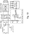
- the voltage across the resonating capacitors is very high particularly in such high-Q operation.
- an Over-Voltage Protection (OVP) mechanism has been implemented, as illustrated by Fig. 10 .
- the voltage V CP is sensed and scaled down by a high-resistance divider network to voltage levels suitable for the comparator operation.
- the scaling of V CP and the value of the reference voltage, V ref are determined according to the highest voltage allowed across the capacitor C P , i.e., across the coupling plates.
- the comparator output is fed to the primary's controller disabling the gate drive signals (Q 1 -Q 4 ), and as a result the system is turned off, until it is being reset. This also allows avoiding undesired safety concerns due to arcing and high electric fields around the coupling plates.
- the coupling plates have been designed symmetrically, such that each plate is 30x30cm.
- the full-bridge inverter has been implemented with GaN power devices operable in several MHz. The overall nominal operating conditions and parameters of the experimental prototype are summarized in Table I.
- the first step of the experimental validation has been carried out by characterizing the inductance of the variable inductor, and the resulting operating frequency of the CPT prototype as a function of the bias current.
- Fig. 11 shows the measured results for varying the bias current in the range of 0 to 2 A. It can be seen that in the vicinity of the nominal operating conditions the inductance and operating frequency f 0 are approximately 75 ⁇ H and 1.2 MHz, respectively, for a bias current of 0.5 A.
- Fig. 12B and Fig. 12C show zoomed-in views of the tuning process with the waveforms of the switching nodes voltages and resonant currents upon initialization and the end ( Fig. 12C ) of the tuning process.
- the switching frequency increases from 892 kHz to 1.2 MHz.
- the output parameters ( I S and V S ) also increase by more than 2.5 times, delivering more energy to the load, while the transfer efficiency has improved considerably (over 25% improvement).
- the primary current I P is slightly lagging the primary voltage V P , which is the necessary condition to enable soft-switching operation.
- the experimental prototype has been also tested for a target power of 10 W over various output load resistances, whereas the coupling capacitance C M ⁇ 20 pF, as shown in Fig. 13A .
- a virtually constant power delivery is obtained throughout the load range.
- the coupling capacitance has been varied to demonstrate the closed-loop operation under variations in the distance or displacement of the coupling plates.
Landscapes
- Engineering & Computer Science (AREA)
- Power Engineering (AREA)
- Computer Networks & Wireless Communication (AREA)
- Inverter Devices (AREA)
- Transceivers (AREA)
- Dc-Dc Converters (AREA)
Description
- The present invention relates generally to the field of Wireless Power Transfer (WPT). More specifically, the invention relates to a system for efficiently and wirelessly performing Capacitive Power Transfer (CPT) using of adaptive matching networks.
- Today, there is a growing demand for mobile power, which is essential to keep highperformance devices available for extended periods or even continuously. Wireless power transfer (WPT) technology potentially provides energy at all times, and reduces the dependency of weight-sensitive and volume-sensitive mobile and portable applications in bulky batteries as a reliable main source of energy.
- One of the WPT solutions is capacitive power transfer (CPT) approach. CPT is an alternative near-field power transfer method to the well know magnetic field based approaches. One of the more attractive advantages of capacitive-based WPT is the avoidance of undesired Eddy currents and electromagnetic interfaces (EMI) that are associated with magnetic-based WPT solutions. In addition to efficiency improvements, CPT systems are potentially of lower volume and their construction is simple.
- A main challenge of general near-field WPT systems and in CPT in particular, is that the power transfer capability and efficiency depend on the distance and alignment between the transmitting and receiving sides. In addition, the coupling coefficient of the transfer medium and load conditions are sensitive to changes in environmental conditions, component aging and temperature drifts, which dramatically decreases the power transfer capabilities of the system. Reducing the sensitivity of the WPT system to variations can be alleviated by designing matching networks that provide loose coupling between the transmitting and receiving sides. However, in this solution, the system characteristics still strongly depend of the component values and the precision of the switching (operating) frequency. To fully disengage the system's characteristics from any drifts, changes and variations, a closed-loop active compensation is essential.
- Several methods to reduce the effects of components and medium variations of WPT systems have been proposed for general power transfer, which can also be adapted to CPT. These include: frequency tuning, compensation networks impedance matching, and post regulation DC-DC conversion. In frequency tuning approach, the switching frequency is adjusted to track the resonant frequency, which results in optimal operating conditions. However, since the allowed frequency range for energy transfer is quite narrow, this solution alone does not accommodate wide variations.
- In impedance matching methods, the resonant inductor and capacitor can be adjusted at a fixed frequency. Thus, the output voltage/current can be regulated by actively adjusting the matching network impedance. The latter provides flexibility for regulating the transferred power to the load, but requires additional control circuitry and potential degradation of the overall efficiency. Although existing closed-loop methods can overcome some system variations and can extend the power delivery range, a single control method is not sufficient to guarantee reliable operation of WPT systems.
- Magnetic field based WPT and in particular magnetic resonance, combined control methods has been proposed, however, a closed-form control mechanism for CPT has not been addressed.
- It is an object of the present invention to provide a multi-loop controller for capacitive-based WPT systems that compensates for the variations of multiple cross-coupling interactions between the transmitting and receiving sides.
- It is another object of the present invention to provide an adaptive multi-loop controller for CPT technology, which compensates on the fly for variations of source and the load circuits, coupling interface (distance and/or alignment) and matching networks.
- Other objects and advantages of this invention will become apparent as the description proceeds.
- Prior art Wireless Power Systems are disclosed, for example, in
WO 2016/161280 A1 or inUS 2014/139034 A1, and are described by SINHA SREYAM ET AL in "Active variable reactance rectifier - A new approach to compensating for coupling variations in wireless power transfer systems" or by MOSTAFA TAREK M ET AL in "Wireless battery charging system for drones via capacitive power transfer". - A controlled wireless Capacitive Power Transfer (CPT) system, based on adaptive matching networks, which comprises:
- a) a primary power transmitter side for wirelessly transmitting power to a secondary power receiver side via coupling plates having mutual capacitance CM ,
the primary side comprises:- a.1) a power source connected to a power driver operating a determined switching frequency fsw ;
- a.2) a primary adaptive matching network consisting of a primary resonant circuit with a bias-controlled variable primary inductor serially connected to the mutual capacitance CM and a capacitor, parallely connected to the mutual capacitance CM, for regulating the current flowing to the secondary side via the mutual capacitance CM;
- a.3) a primary controller consisting of:
- a.3.1) a first control loop, for adjusting the switching frequency fsw to compensate for changes in the impedance of the primary matching network, whenever the mutual capacitance CM changes;
- a.3.1) a second control loop, for adjusting the resonant frequency of the primary resonant circuit to track the switching frequency fsw by providing appropriate bias to the primary inductor and changing the resonant frequency of the primary resonant circuit;
- b.1) a rectifier circuit connected to a load and operating at resonant frequency of the primary resonant circuit;
- b.2) a secondary adaptive matching network connecting between the mutual capacitance CM and the rectifier circuit and consisting of a secondary resonant circuit with a bias-controlled variable secondary inductor serially connected to the mutual capacitance CM and a parallel capacitor parallely connected to the mutual capacitance CM, for matching the impedance of the secondary matching network;
- b.3) a secondary controller consisting of:
b.3.1) a control loop, for adjusting the impedance of the secondary matching network to match the resonant frequency of the primary resonant circuit by providing appropriate bias to the secondary inductor.
- The first control loop may be implemented by a DPLL.
- The switching frequency may be synthesized to continuously follow the resonant frequency of the primary side, in response variations of the system parameters.
- The power delivery from the primary side to the secondary side is disengaged from cross-coupling interactions between the transmitting and receiving sides and variations of the electrical circuits and capacitive medium.
- In one aspect, power delivery from the primary side to the secondary side is adaptively tuned to satisfy required power conditions at either the coupling plates terminals or at the output terminals.
- In one aspect, power delivery from the primary side to the secondary side is adaptively tuned by adjusting the operating frequency and varying the value of one or more reactive components.
- The adaptive matching network may include a bias controlled or a command controlled variable capacitance, which may be varied continuously, or in segments.
- The power driver on the primary side may be a full-bridge inverter.
- The primary side may be adapted to deliver constant current to the secondary side.
- The resonant frequency of the primary and secondary resonant circuits may be adjusted by changing the values of the inductors or parallel capacitors or both.
- In one aspect, the drive (the operating) frequency tracks the resonant frequency on the fly, and the transmitted power is regulated by the resonant circuit characteristics.
- The resonant network may comprise a plurality of inductors and capacitors in either series connection, parallel connection, or a combination of both connections.
- The resonant network in each side may comprise two or more variable components, such as inductors or capacitors or a combination of both.
- In one aspect, the bandwidth of the first control loop has the highest bandwidth, to obtain the fastest response, and the bandwidth of the control loop of the secondary side is lower than the bandwidth of the first control loop.
- The bandwidth of the second control loop may have the lowest bandwidth.
- The bias driver may be realized by either a linear regulator or by a buck converter.
- The current of the bias driver may be regulated by an internal closed-current-loop.
- Optimal power transfer conditions may be obtained when the phase difference between the primary's and secondary's resonant frequencies equals 90°.
- The control loops may be characterized by their bandwidth difference.
- In one aspect, the transmitted signal at the primary side output terminals is modulated, for transmitting power to a plurality of loads, each corresponding to a secondary side, such that each load will receive the transmitted power at a different frequency.
- An optional forth feedback loop may be employed to facilitate direct regulation of the output characteristics through back communication from the secondary side to the primary side, wherein the optional forth feedback loop adjusts the signal transmitted from the primary side, until a desired transmitted signal is obtained.
- In one aspect, the secondary side circuit comprises an independent tuning circuit.
- A method for controlling power transfer in a Capacitive Power Transfer (CPT) system consisting of a primary power transmitter side for wirelessly transmitting power to a secondary power receiver side via coupling plates having mutual capacitance CM, and primary and secondary matching networks, comprising the steps of:
- a) upon initiating the tuning of the primary and secondary matching network, determining the switching frequency fsw , and the variable primary and secondary inductors as default set of pre-loaded values;
- b) tuning the switching frequency of the primary driver a first control loop;
- c) detecting a phase difference between the signals VP and VCP and maintaining a 90° phase angle between VP and VCP at all times;
- d) whenever the detected phase difference between the signals is not 90°, generating an error signal to create a new switching frequency, until the switching frequency equals the resonant frequency;
- e) detecting a phase difference between VS and VCS and maintaining the phase difference at 90°;
- f) adjusting the secondary side's inductance value LS to tune the secondary matching network, according to the switching frequency fsw of the primary side;
- g) providing a correction signal to adjust the inductance value LS, until the network is at resonance (until fsw =f 0) and the phase difference between the signals VS and VCS equals 90°; sensing the regulated current Ireg from the primary circuit and comparing the regulated current to a target/reference current; and
- h) generating a correction signal that adjusts the inductance LP through bias winding until the desired current is achieved.
- In the drawings:
-
Fig. 1 schematically illustrates a schematic block diagram of a double-sided LC capacitive WPT system with an adaptive multi-loop controller, according to an embodiment of the invention; -
Fig. 2 shows typical waveforms of a of a CPT system; -
Fig. 3 illustrates a simplified behavioral model for the output side of the CPT system, according to an embodiment of the invention; -
Fig. 4 is a flowchart of the tuning procedure that utilizes the three control loops, according to an embodiment of the invention; -
Figs. 5A-5C are simplified functional block diagrams that describe the dynamic behavior of this self-tuned system, according to an embodiment of the invention; -
Fig. 6A shows one possible implementation of a variable inductor; - 6B illustrates Passing DC current through the auxiliary winding and saturating a portion of the core, resulting in variable inductance;
-
Fig. 7 illustrates possible realization of phase detection for both the transmitting and receiving sides; -
Fig. 8A shows the phase difference between the signals under resonant operation; -
Fig. 8B shows the phase difference between the signals when the resonant condition is not satisfied; -
Fig. 9 shows a current-sensing circuit, based on a peak detector mechanism, which consists of a simple half wave rectifier configuration; -
Fig. 10 illustrates the implementation of an Over-Voltage Protection (OVP) mechanism; -
Fig. 11 shows the measured results for varying the bias current in the range of 0 to 2 A; -
Fig. 12A shows the behavior of the primary's current IP and the secondary's voltage VS during tuning process for an input voltage Vin =30 V; -
Fig. 12B shows zoomed-in views of the tuning process with the waveforms of the switching nodes voltages and resonant currents upon initialization; -
Fig. 12C shows zoomed-in views of the tuning process with the waveforms of the switching nodes voltages and resonant currents at the end of the tuning process; -
Fig. 13A shows the effectiveness of the new multi-loop controller for a target power of 10 W over various output load resistances, with coupling capacitance CM ≈20 pF; -
Fig. 13B shows the effectiveness of the new multi-loop controller for a target power of 10 W over various output load resistances for varying coupling capacitance CM (varying airgaps between coupling plates of CM); -
Fig. 14 shows an alternative method for the adaptation or tuning of the matching networks, according to another embodiment of the invention; and -
Fig. 15 shows an additional embodiment, according to which an optional fourth feedback loop is added for the cases that direct regulation of the secondary's output voltage is desired. - The present invention proposes an adaptive multi-loop controller for capacitive wireless power transfer (WPT) systems which are based on adaptive matching networks, in which power is wirelessly transmitted from a primary side to a secondary side. The multi-loop controller combines continuous frequency tracking and matching networks tuning on both the primary (power transmitter) side and the secondary (power receiver) side, to regulate a target current/power to the receiving side at best power transfer conditions. This allows effectively disengaging the power delivery capabilities from the cross-coupling interactions between the transmitting and receiving sides, variations of the electrical circuits and capacitive medium. The proposed controller disengages the power delivery capabilities from drifts or variations, which enables spatial freedom of the transferred energy to the receiving side. The proposed controller uses continuous tuning of the switching frequency to the resonant frequency, and adjusts both the transmitter's and receiver's matching networks such that the best power transfer conditions are obtained for any given combination of distance, displacement, misalignment or component values. The proposed controller uses tuned network realization that is based on a variable inductor (rather than relays or semiconductor switches), and therefore enables continuous self-tuned impedance matching. Alternatively, the tuned network realization may be based on variable capacitance or a combination of variable capacitance and variable inductance, to allow continuous self-tuned impedance matching.
-
Fig. 1 schematically illustrates a schematic block diagram of a double-sided LC capacitive WPT system with an adaptive multi-loop controller, according to an embodiment of the invention. The double-sided LC capacitive WPT system uses Closed-Loop Tuning with adaptive multiloop controller, through a resonant double-sided LC matching network. It should be noted, however, that the control algorithm is applicable for any CPT system. -
Fig. 14 shows an alternative method for the adaptation or tuning of the matching networks, according to another embodiment of the invention. In this embodiment, the system may also include variable capacitance, either in continuous or segmented arrangement. The addition varying capacitance, continuously or in segments, can also be utilized as an additional, independent, control loop that improves the efficiency or power transfer conditions of the resonant networks. - The
system 10 is driven by a full-bridge inverter 11 on the primary side (Transmitter), and the load is fed via a diode rectifier 12 (a rectifier circuit) that is connected to the secondary's network (Receiver). Considering that the self-capacitances and the mutual coupling capacitance CM are lower than the total parallel capacitances CP and CS, and that the drive frequency is near the matching networks' resonant frequency (i.e.,
- When resonant operation is satisfied, the primary current IP depends on the output voltage, and the secondary current, IS , depends on the input voltage, and thus with the aid of system parameters, the currents can be expressed as

-
Fig. 2 shows typical waveforms of a of a CPT system. As described, while the primary and secondary voltages VP and VS are square waves, the currents are sinusoidal due to high-Q operation of the circuit. Since a full-bridge inverter 11 is used at the front-end, the primary voltage VP varies between Vin to -Vin. It can be also seen, that for both the primary and secondary sides, the current is in phase with the voltage, whereas the secondary voltage VS lags the primary voltage VP by 90°. - From (1), it can be seen that the double-sided
LC CPT system 10 can be described by a two-port network with gyrator characteristics [34], with a trans-conductance gain G.Fig. 3 illustrates a simplified behavioral model for the output side of theCPT system 10. This implies that the dynamic behavior of the overall system can be characterized as a voltage-dependent current source. By employing fundamental harmonics approximation method on (1), the average value of the output current Iout is expressed as a function of the input voltage Vin as follows

-
Fig. 1 . - In light of the above, an adaptive controller that monitors, tunes, and enables to continuously deliver constant current to the receiving side is proposed by the present invention.
- Returning back to
Fig. 1 , power regulation is facilitated by three major control loops as shown inFig. 1 , with twocontrol loops third loop 15 is located at the secondary circuit. The control loops are distinguished by their control objectives and bandwidth requirements, such that the operating characteristics of the WPT system are satisfied. Thefirst control loop 13 resembles in structure to a digital phase-locked loop (DPLL) that synthesizes a switching frequency fsw , which continuously follows (tracks) the resonant frequency of the primary side f0 , even under variations of the system parameters. This ensures in this LC configuration that the power conversion characteristics of the networks are optimized. - Compensating for changes in the mutual coupling capacitance CM coupling medium due to movements between CM plates (i.e., movement of the secondary circuit with respect to the primary circuit) requires compensation by varying the drive frequency off the specific optimized point and correcting the network parameters accordingly. This can be achieved by adjusting network inductor, capacitor or both. In this example, an approach based on variable inductor is employed.
- In the example of
Fig. 1 , the primary adaptive matching network 17 consists of a primary resonant circuit with a bias-controlled variable primary inductor LP, serially connected to the mutual capacitance CM and a capacitor CP, parallely connected to the mutual capacitance CM, for regulating the current flowing to said secondary side via the mutual capacitance CM. The secondary adaptive matching network 18 consists of a secondary resonant circuit with a bias-controlled variable secondary inductor LS, serially connected to the mutual capacitance CM and a capacitor CS, parallely connected to the mutual capacitance CM. However, it should be noted that in a more general configuration, the primary adaptive matching network 17 may consist of a primary resonant circuit with a first bias-controlled variable reactance (which may be a variable capacitor or a variable inductor or a combination thereof), serially connected to the mutual capacitance CM and a second bias-controlled variable reactance (which may be a variable capacitor or a variable inductor or a combination thereof), parallely connected to the mutual capacitance CM, for regulating the current flowing to said secondary side via the mutual capacitance CM. The secondary adaptive matching network 18 may consist of a secondary resonant circuit with a bias-controlled variable a third bias-controlled variable reactance (which may be a variable capacitor or a variable inductor or a combination thereof), serially connected to the mutual capacitance CM and a fourth bias-controlled variable reactance (which may be a variable capacitor or a variable inductor or a combination thereof), parallely connected to the mutual capacitance CM. - The
second control loop 14 adjusts the resonant frequency of the primary resonant circuit to track the switching frequency fsw by providing appropriate bias to the primary inductor and change resonant frequency of the primary resonant circuit. Thesecond control loop 14 comprises a current compensator and a tuning unit, that adjusts the inductance value of LP such that a target constant current (as well as power) is obtained. This transforms the primary circuit into a self-tuned architecture, in which the drive frequency tracks the resonant frequency on the fly, and the transmitted power is regulated by the resonant network's characteristics. - A
third compensation loop 15, located in the receiver side, comprises a tuning unit that adjusts the inductance value LS of the secondary side inductance, according to the resonant operating frequency of the system, which is determined by thefirst control loop 13. -
Fig. 15 shows an additional embodiment, according to which an optional fourth feedback loop is added for the cases that direct regulation of the secondary's output voltage is desired. As can be seen that in this case, the reference assignment for the transmitted current is controlled by information from the output of the secondary side. In this example, the output voltage Vout across the load is sampled and wirelessly transmitted tocurrent control loop 14. -
Fig. 4 is a flowchart of the tuning procedure that utilizes the three control loops 13-15. When the tuning procedure is initiated, at step 41 a default set of pre-loaded values are used to determine the switching frequency fsw , and the variable inductors LP and LS. These values are determined by the target operating conditions of the system. The adaptive tuning operation is conducted per feedback loop. First, the switching frequency to drive the full-bridge is being tuned by the first control loop (DPLL) 13, where its inputs are the voltages VP and VCP, such that a phase difference between the signals is detected atstep 42. To guarantee that the switching frequency fsw follows the resonant frequency f0 for any given variations of the primary circuit, 90° phase angle between VP and VCP is maintained at all times. In case when the detected phase difference between the signals is not 90°, an error signal is generated to the DPLL frequency compensator and generates new switching frequency until fsw = f 0. - At the
next step 43 of the tuning process, a phase difference between VS and VCS is detected and is maintained at 90° and the secondary side's inductance value, LS is adjusted to tune the secondary matching network, according to the switching frequency fsw of the primary side. The correction signal in this case adjusts the inductance value LS rather than the drive frequency fsw (which has been determined by the primary circuit). This is carried out by a driver that feeds the bias winding of the inductor, until the network is at resonance (until fsw =f0) and the phase difference between the signals VS and VCS equals 90°. At thefinal step 44, the regulated current Ireg (seeFig. 1 ) from the primary circuit is sensed and compared to a target/reference current. The tuningunit 16 generates a correction signal that effectively adjusts the inductance LP through bias winding until the desired current is achieved. It should be noted that the inductance tuning (to adjust the transfer current) results in different resonant characteristics of the system, and consequently, thefrequency tuning loop 13 operates to lock the switching frequency to the new resonant frequency. - To satisfy proper operation with reasonable dynamics of this multi-loop scheme, the compensators are decoupled by their bandwidth. The
frequency tracking loop 13, is designed to be with highest bandwidth within the controller, i.e., responds the fastest among the multiple control loops. The frequency loop is followed by the secondary'sloop 15, which is also designed to be a relatively high-bandwidth loop compared tocurrent control loop 14. This design assures that the faster loop is virtually transparent to its following loops and by doing so, significantly simplifies the system dynamics and complexity of the compensators. -
Figs. 5A-5C are simplified functional block diagrams that describe the dynamic behavior of this self-tuned system. The block diagrams comprise both linear and non-linear transfer functions to reflect the specific operation of each 'transformation unit' (i.e. 'block'). -
Figs. 5A-5B of the primary control circuit includes two major loops to satisfy current sourcing behavior to the transfer plates.Fig. 5C illustrates a third, independent loop that is located at the secondary side, to adjust the receiving network to the signal's frequency. In addition, for both the primary and secondary circuits, the bias driver of the variable inductors is designed as a closed feedback loop configuration to maintain a forced current control. This enables to reduce the order of the outer feedback loop, and therefore, allows simple stabilization the overall system. By employing self-calibrating frequency loop and adjusting the system parameters, regulation of the primary's output current, Ireg , can be achieved at the same time that the system is kept at resonance (while soft-switching conditions are met). - Starting from the left side of
Fig. 5A , Iref is a proportional representation of the target regulated current from the primary to the secondary, where Ic,P represents the correction signal generated by the current compensator, and Ie_Bias,P is the error signal of the inner bias current loop. Kmod stands for the transfer ratio of the modulator, i.e., bias current correction signal, Ic_Bias,P to duty-cycle of the bias current driver. The bias driver has been realized by a buck converter, and its transfer function is represented in the block diagrams by BP. The bias current for the inductor LP can be expressed as


- HLP represents the bias winding such that the relationship between the bias current and the primary side inductance is

- The relationship of HLP(IBias,P) can be obtained by experimental measurements, advanced simulation tools such as Maxwell, or by analytical analysis. Thus, a local linearization around the operating point determines the non-linear small signal of HLP as follows

-
Fig. 5B details the transfer characteristics of Kf. The output of HLP dictates the resonant frequency f0 of the CPT system such that
- Considering HLP(IBias) is constant, a derivation of the large signal Kres,P(LP) around the operating point yields the small signal transfer function of the resonant tank [35]:


- Therefore, the zero frequency is always higher than the pole frequency. By doing so, the stability of the Digital Controlled Oscillator (DCO) is improved since its phase margin can be increased compared to a simple LPF. The voltage Vf is then translated by the Digital Controlled Oscillator (DCO) unit to a drive frequency for the power-stage combined with the LC tank, which in turn generates the desired target current.
-
Fig, 5C is a functional block diagram of the secondary's control loop. The operating resonant frequency of the system is compared by a phase detector to the resonant frequency of the secondary, f 0,s . It should be noted that for stable operating CPT system f 0,S =fsw= f 0. Similar to the above given relationships of the primary side, the output signal of the secondary's phase detector VPD,S is given by
- To assure reasonable dynamics of the multiple feedback loops, for a given quality factor Q, assuming that fsw is locked on f 0 the bandwidth of this loop is determined as follows

- The secondary's control loop is also relatively a high-bandwidth loop and is set as a fraction of BW1, typically a good practice is one-third (1/3) to one-tenth (1/10). The outer current loop is set to be with slowest dynamics within the controller, typically one-ninth (1/9) to one-fiftieth (1/50) of the switching frequency of the system. By doing so, the loops are decoupled and tuning procedure does not depend on preceding information or data of the system to facilitate closed-loop operation.
-
Fig. 6A shows one possible implementation of a variable inductor, where a magnetic structure is described with the ability to change the inductance of the inductor independent of other power transfer circuit parameters. The magnetic structure comprises an E-core type magnetic element, whereas the primary inductor is constructed on the middle, gapped leg. The bias/control winding is formed on the outer, non-gaped, and their windings are connected in series but with opposite polarity. By doing so, the AC coupling between the center leg and the bias winding is cancelled. Passing DC current through the auxiliary winding would partially saturate this portion of the core, resulting in variable inductance, as illustrated byFig. 6B . - The inductance value L can be found using several design parameters such as: number of turns n, air-gap lg , and the effective magnetic path length le , and thus, the expression of L can be expressed as


- When designing closed-loop resonant based WPT systems, limit-cycle oscillations which resulted from the presence of the quantizing units of the controller, such as analog-to-digital converter (ADC) and the DCO (assuming the compensators does not add quantization error) must be considered. Primary cause for limit-cycle oscillations in resonant converters is that the input-output gain is not constant and varies as a function of the frequency. In capacitive WPT systems, which operate at resonance, the effective impedance is very high due to the coupling plates, and a very high parallel quality factor Q is considered, which translates to a very high voltage gain. In addition, one of the key parameters to successfully regulating the power is that the system locks on the resonant frequency. However, to guarantee optimal power transfer conditions, soft-switched operation should be satisfied, so as to generate a drive frequency which is slightly above the resonant frequency. This objective requires very sensitive calibration which may also result in limit-cycle oscillations, since in resonant converters the frequency resolution highly depends on operating conditions and the location of the drive frequency with respect to the network's resonance.
- Since the quality factor Q is not constant and depends on the capacitive medium characteristics (distance, alignment, etc.), it affects the input-output gain of the system. Therefore, to assure proper operation, worst case of the resolution sensitivity should be considered, i.e., the highest Q that the system might have. Thus, the ADC and DCO units have been designed such that limit-cycle oscillations are remedied. A key criterion for determining the existence of limit-cycle oscillations in resonant systems relies on the comparison between the LSB value (i.e., resolution) of the ADC and the output signal variation due to a LSB change of the control, i.e., a necessary condition for no limit cycles is that the variation of the output ΔSout, due to a LSB change of control is smaller than the ADC resolution ΔADC [41]

- Digitally synthesized frequency is normally carried out by timers that are programmed to reset at a desired value, while maintaining a fixed 50% duty ratio. The generated frequency can be expressed by


- From (20), it can be observed that the frequency steps of the DCO are limited by the system clock frequency, and increase as the square of the operating frequency. Consequently, at lower running frequency, the frequency resolution would be finer than what can be achieved at a higher frequency. In the case that finer resolution than the one obtained by the system DCO is required, an effective fast dynamics and low distortion frequency dithering procedure has been employed.
-
Fig. 7 illustrates possible realization of phase detection for both the transmitting and receiving sides. Typically, in capacitive WPT systems the voltages of the resonators are significantly higher than the operating voltage levels of the controller periphery. Therefore, the input voltages VP and VCP (VS and VCS) are scaled down using a simple high-resistance divider network to a voltage level suitable for the phase detector unit. The sensed high-frequency scaled voltages are fed into a comparator that acts as zero-cross detector. Then, the digital represented signals of the zero-cross detection are fed into an exclusive-or (XOR) operator. Inherently, under resonant operation the phase difference between the signals is 90°, as shown inFig. 8A . Consequently, the output of the XOR, VXOR, is a square wave with 50% duty-ratio and a doubled frequency. VXOR is passed through a LPF, resulting in a voltage that is proportional the phase angle magnitude, which for the resonant operation equals exactly VDD /2 (assuming the voltage supply of logic is VDD), which is then synthesized to the resonant operating frequency. In case that resonant operation is not satisfied (as shown inFig. 8B ), where the duty-ratio of VXOR is 25%, thus the output of the filter is lower than VDD /2, and as a result, a corrected switching frequency is synthesized until it equals to the resonant frequency. Practically, any phase shift between the two measured voltage signals results in some constant offset that should be calibrated out. Thus, to minimize phase offset errors, similar voltage scaling should be employed for both signals as much as possible. - The multi mixed-signal controller requires various measurements of the operating conditions in the WPT system. A key measurement of the system is the regulated current, Ireg , to the capacitive medium. However, this high-frequency current is not trivial to measure and sensing techniques such as current transformer and filter-sense may result in a complex sensing circuitry. The current-sensing employed by the present invention is based on a peak detector mechanism which consists of a simple half wave rectifier configuration, as shown in
Fig. 9 . The sensed current converted to a proportional voltage suitable signal, Vsns, by flowing through the resistor Rsns[46]. The peak detector is implemented around an operational amplifier to compensate for the voltage drop on the rectifying diode D. To reduce the losses related to the diode, a Schottky diode is used primarily due to its relatively low forward voltage and zero reverse recovery time, further improving the sensor performance. The time constant of the peak detector is selected approximately ten times the period of the sensed sinusoidal signal to both filter out the ripple, and smoothly follow the peak value of the signal. The peak detector configuration enables reduced sampling rate requirements of the ADC, and therefore reduces its power consumption. Another benefit of this sensing circuitry is that it also provides information for over-current protection (OCP) and can be used for fault protection of the system. - A key feature of the sensors of the implemented CPT system in particular of the current sensing circuitry is to provide an isolated ground reference level to the sense resistor as well as the peak detector circuit (
Fig. 9 ). By doing so, the limitations due to sensing relative to a floating voltage node are eliminated, in addition, this configuration also improves the signal to noise ratio. - As mentioned in the phase detection, the voltage across the resonating capacitors is very high particularly in such high-Q operation. Thus, to avoid any potential failure risks of the CPT system due to over-voltage in the vicinity of the coupler, an Over-Voltage Protection (OVP) mechanism has been implemented, as illustrated by
Fig. 10 . Similar to phase detection process, the voltage VCP is sensed and scaled down by a high-resistance divider network to voltage levels suitable for the comparator operation. The scaling of VCP and the value of the reference voltage, Vref, are determined according to the highest voltage allowed across the capacitor CP, i.e., across the coupling plates. For a case that VCP is higher than the reference voltage, the comparator output is fed to the primary's controller disabling the gate drive signals (Q 1 -Q 4 ), and as a result the system is turned off, until it is being reset. This also allows avoiding undesired safety concerns due to arcing and high electric fields around the coupling plates. - The coupling plates have been designed symmetrically, such that each plate is 30x30cm. The matching networks have been also designed to be symmetrical; in nominal operation the inductors' values are set to LP =Ls ≈75 µH and the matching capacitors CP =Cs =250 pF. The operating frequency slightly above the resonance f0 ≈1.2 MHz, guaranteeing soft-switching. High-voltage multilayer SMD ceramic capacitors have been used for the matching capacitors CP and CS. The full-bridge inverter has been implemented with GaN power devices operable in several MHz. The overall nominal operating conditions and parameters of the experimental prototype are summarized in Table I.
TABLE I - EXPERIMENTAL PROTOTYPE PARAMETERS AT NOMINAL OPERATION Parameter Value/Type Input voltage Vin 30 V Output current 1 A Coupling plates 30x30 cm Air-gaps 15-100 mm Full-bridge transistors LMG5200, 80 V, 15 mΩ, Dual Variable inductors LP and LS ~75 µH Capacitors CP and C S250 pF, TDK 810 series Operating frequency f 0 1.2 MHz - The first step of the experimental validation has been carried out by characterizing the inductance of the variable inductor, and the resulting operating frequency of the CPT prototype as a function of the bias current.
Fig. 11 shows the measured results for varying the bias current in the range of 0 to 2 A. It can be seen that in the vicinity of the nominal operating conditions the inductance and operating frequency f0 are approximately 75 µH and 1.2 MHz, respectively, for a bias current of 0.5 A. -
Fig. 12A shows the behavior of the primary's current IP and the secondary's voltage VS during tuning process for an input voltage Vin =30 V. It can be observed that initially, the system is not tuned and the regulated current on the primary side has higher peak amplitude compared to the one at the end of the tuning procedure. This is due to the fact that at the beginning the system is not calibrated and best operating conditions are not satisfied, thus undesired circulating current is drawn from the power source. On the other hand, at the end of the tuning procedure the voltage VS has higher peak amplitude, since the system is calibrated to resonance and is operated under (local) optimal power transfer conditions according to the target current. -
Fig. 12B andFig. 12C show zoomed-in views of the tuning process with the waveforms of the switching nodes voltages and resonant currents upon initialization and the end (Fig. 12C ) of the tuning process. It can be seen that the switching frequency increases from 892 kHz to 1.2 MHz. The output parameters (IS and VS) also increase by more than 2.5 times, delivering more energy to the load, while the transfer efficiency has improved considerably (over 25% improvement). In addition, it can also be noticed that the primary current IP is slightly lagging the primary voltage VP, which is the necessary condition to enable soft-switching operation. - To further demonstrate the effectiveness of the new multi-loop controller for capacitive WPT systems and showcase of the quality of the performance in closed-loop, the experimental prototype has been also tested for a target power of 10 W over various output load resistances, whereas the coupling capacitance CM ≈20 pF, as shown in
Fig. 13A . A virtually constant power delivery is obtained throughout the load range. In the experiment ofFig. 13B the coupling capacitance has been varied to demonstrate the closed-loop operation under variations in the distance or displacement of the coupling plates. The experiment has been conducted with constant load resistance of RLOAD ≈100 Ω, and varying the coupling plates' air-gaps up to the range of 100 mm, this translates to capacitance range of approximately 5 pF to 25 pF. Similar to the variable load test, it can be seen that, aside from measurement deviation, the output power is well regulated at a constant value. These two measurements validate the closed-loop operation of the self-tuned CPT system, which provides regulated power delivery regardless the medium or load variations. - Although embodiments of the invention have been described by way of illustration, it will be understood that the invention may be carried out with many variations, modifications, and adaptations, without exceeding the scope of the claims.
-
- [1] Z. Zhang, H. Pang, A. Georgiadis, and C. Cecati, "Wireless power transfer-An overview," IEEE Trans. Ind. Electron., Early Access, 2018.
- [2] T. Imura and Y. Hori, "Maximizing air gap and efficiency of magnetic resonant coupling for wireless power transfer using equivalent circuit and Neumann formula," IEEE Trans. Ind. Electron., vol. 58, no. 10, pp. 4746- 4752, Oct. 2011.
- [3] T. Langlotz, T. Nguyen, D. Schmalstieg, and R. Grasset, "Next generation augmented reality browsers: Rich, seamless, and adaptive," in Proc. IEEE, vol. 102, no. 2, pp. 155-169, Feb. 2014.
- [4] D. Xu, L. Han, M. Tan, and Y. F. Li, "Ceiling-based visual positioning for an indoor mobile robot with monocular vision," IEEE Trans. Ind. Electron., vol. 56, no. 5, pp. 1617-1628, May 2009.
- [5] S. Li and C. Mi, "Wireless Power Transfer for Electric Vehicle Applications," IEEE Journal of Emerging and Selected Topics in Power Electronics, vol. PP, pp. 1-1, 2014.
- [6] S. Jaegue et al., "Design and implementation of shaped magnetic resonance-based wireless power transfer system for roadway-powered moving electric vehicles," IEEE Trans. Ind. Electron., vol. 61, no. 3, pp. 1179-1192, Mar. 2014.
- [7] K. Wu, D. Choudhury, and H. Matsumoto, "Wireless power transmission, technology, and applications" Proceedings of the IEEE, Vol. 101, no.6, pp. 1271 - 1275, June 2013.
- [8] L. Collins, "Cut the cord," Electron. Syst. Softw., vol. 5, no. 6, pp. 42-46, Jan.-Dec. 2007.
- [9] F. Musavi and W. Eberle, "Overview of wireless power transfer technologies for electric vehicle battery charging," IET Power Electronics, vol. 7, no. 1, pp. 60-66, 2014.
- [10] M. P. Theodoridis, "Effective capacitive power transfer," IEEE Trans. Power Electron., vol. 27, no. 12, pp. 4906-4913, Dec. 2012.
- [11] F. Lu, H. Zhang, H. Hofmann, and C. Mi, "A double-sided LCLC compensated capacitive power transfer system for electric vehicle charging," IEEE Trans. Power Electron., vol. 30, no. 11, pp. 6011-6014, Jun. 2015.
- [12] H. Zhang, F. Lu, H. Hofmann, W. Liu, and C. C. Mi, "A four-plate compact capacitive coupler design and LCLcompensated topology for capacitive power transfer in electric vehicle charging application," IEEE Trans. Power Electron., vol. 31, no. 12, pp. 8541-8551, Dec. 2016.
- [13] F. Lu, H. Zhang, H. Hofmann, C. Mi, "A loosely coupled capacitive power transfer system with LC compensation circuit topology," Proc. IEEE Energy Convers. Congr. Expo. (ECCE), pp. 1-5, 2016.
- [14] F. Lu, H. Zhang, C. Mi, "A two-plate capacitive wireless power transfer system for electric vehicle charging Applications," IEEE Trans. Power Electron, vol. 33, no. 2, pp. 946-969, Aug. 2017.
- [15] F. Lu, H. Zhang, H. Hofmann, and C. Mi, "A double-sided LC compensation circuit for loosely-coupled capacitive power transfer," IEEE Trans. Power Electron., vol. 33, no. 2, pp. 1633 - 1643, Feb. 2017.
- [16] J. Dai and D.C Ludois, "A survey of wireless power transfer and a critical comparison of inductive and capacitive coupling for small gap applications," IEEE Trans. Power Electron, vol. 30, no. 11, pp. 6017-6029, Nov. 2015.
- [17] B. Lee, M. Kiani, and M. Ghovanloo, "A triple-loop inductive power transmission system for biomedical applications," IEEE Trans. Biomed. Circuits Syst, vol. 10, no. 1, pp. 138-148, Feb. 2016.
- [18] Y. Lim, H. Tang, S. Lim, J. Park, "An adaptive impedance-matching network based on a novel capacitor matrix for wireless power transfer," IEEE Transactions on Power Electronics, vol. 29, no. 8, pp. 4403-4413, August 2014.
- [19] T.C. Beh, M. Kato, T. Imura, S. Oh and Y. Hori, "Automated impedance matching system for robust wireless power transfer via magnetic resonance coupling," IEEE Transactions on Industrial Electronics, vol. 60, no. 9, pp. 3689-3698, September 2013.
- [20] H. Li, J. Li, K. Wang, W. Chen, and Y. Xu, "A maximum efficiency point tracking control scheme for wireless power transfer systems using magnetic resonant coupling," IEEE Trans. Power Electron., vol. 30, no. 7, pp. 3998-4008, Jul. 2015.
- [21] P. Si, A. P. Hu, S. Malpas, D. Budgett, "A frequency control method for regulating wireless power to implantable devices," IEEE Trans. on Biomedical Circuits and Systems., vol. 2, no. 1, pp. 22- 29, March. 2008.
- [22] T. D. Yeo, D. Kwon, S. T. Khang, and J. W. Yu, "Design of maximum efficiency tracking control scheme for closed-loop wireless power charging system employing series resonant tank," IEEE Trans. Power Electron., vol. 32, no. 1, pp. 471-478, Jan. 2017.
- [23] K. Lu, S. K. Nguang, S. Ji, and L. Wei, "Design of auto frequency tuning capacitive power transfer system based on class-.
- [24] M. Kline, I. Izyumin, B. Boser, and S. Sanders, "Capacitive power transfer for contactless charging," in Proc. IEEE Appl. Power Electron. Conf. Expo., 2011, pp. 1398-1404.
- [25] B. H.Waters, A. P. Sample, J. R. Smith, "Adaptive impedance matching for magnetically coupled resonators," in Proc. Prog. Electromagn. Res. Symp., 2012, pp. 694-701.
- [26] M. Pinuela, D. C Yates, S. Lucyszn, and P. D. Mitcheson, "Maximizing dc-to-load efficiency for inductive power transfer," IEEE Trans. Power Electron., vol. 28, no. 5, pp. 2437-2447, May 2013.
- [27] S. Sinha, A. Kumar, S. Pervaiz, B. Regensburger and K.K. Afridi, "Design of efficient matching networks for capacitive wireless power transfer systems," Proceedings of the IEEE Workshop on Control and Modeling for Power Electronics (COMPEL), Trondheim, Norway, June 2016.
- [28] A. Kumar, S. Sinha, A. Sepahvand, K. K. Afridi, "Improved design optimization for high-efficiency matching networks," IEEE Transactions on Power Electronics, vol. 33, no. 1, pp. 37-50, Jan 2018.
- [29] S. Sinha, A. Kumar, K. K. Afridi, "Improved design optimization of efficient matching networks for capacitive wireless power transfer systems," in Proc. IEEE Appl. Power Electron. Conf. Expo. (APEC), Mar. 2018, pp. 3167-3173.
- [30] J. Kim and J. Jeong, "Range-adaptive wireless power transfer using multiloop and tunable matching techniques," IEEE Trans. Ind. Electron., vol. 62, no. 10, pp. 6233-6241, Oct. 2015.
- [31] J.G. Hayes and M.G. Egan, "Rectifier-compensated fundamental mode approximation analysis of the series parallel LCLC family of resonant converters with capacitive output filter and voltage-source load," Proceedings of the IEEE Power Electronics Specialists Conference (PESC), Charleston, SC, July 1999.
- [32] S. Y. R. Hui, W. Zhong, and C. K. Lee, "A critical review of recent progress in mid-range wireless power transfer," IEEE Trans. Power Electron., vol. 29, no. 9, pp. 4500-4511, Sep. 2014.
- [33] R.L. Steigerwald, "A comparison of half-bridge resonant converter topologies," IEEE Transactions on Power Electronics, vol. 3, no. 2, pp. 174-182, April 1988.
- [34] Y. H. Sohn, B. H. Choi, G. H. Cho, and C. T. Rim, "Gyrator-Based Analysis of Resonant Circuits in Inductive Power Transfer Systems," IEEE Transactions on Power Electronics, vol. 31, no. 10, pp. 6824-6843, Oct. 2016.
- [35] S. Ben-Yaakov and M. M. Peretz, "A self-adjusting sinusoidal power source suitable for driving capacitive loads," IEEE Trans. Power Electron., vol. 21, no. 4, pp. 890-898, Jul. 2006.
- [36] E. Abramov, T. Vekslender, O. Kirshenboim, and M. M. Peretz, "Fully-integrated digital average current-mode control voltage regulator module IC," IEEE Journal on Emerging and Selected Topics in Power Electronics, vol. 6, no. 2, pp. 549-562, Jun. 2018.
- [37] K. Kalita, J. Handique, T. Bezboruah, "Modelling and behavioral simulation of a high-speed phase-locked loop for frequency synthesis," IET Signal Processing, vol. 6, no. 3, pp. 195-204, May 2012..
- [38] S. S. Ahsanuzzaman, T. McRae, M. M. Peretz, and A. Prodic, "Low volume buck converter with adaptive inductor core biasing," in Proc. IEEE Appl. Power Electron. Conf. Expo. (APEC), Feb. 2012, pp. 335-339.
- [39] O. Ezra and M. M. Peretz, "Magneto-electro-mechanical modeling of magnetic actuation systems," in Proc. IEEE Applied Power Electronics Conference and Exposition (APEC), 2015, pp. 2628-2634.
- [40] S. Ben-Yaakov, M. M. Peretz, "Simulation bits: a SPICE behavioral model of non-linear inductors," IEEE Power Electronics Society Newsletter, Fourth Quarter, pp. 9-10, 2003.
- [41] M. M. Peretz and S. Ben-Yaakov, "Digital control of resonant converters: resolution effects on limit cycles," IEEE Trans. on Power Electronics, vol.25, no.6, pp.1652-1661, 2010.
- [42] S. R. Sanders, "On limit cycles and describing function method in periodically switched circuits," IEEE Trans. Circuits Syst., vol. 40, no. 9, pp. 564-572, Sep. 1993.
- [43] H. Peng, A. Prodic, E. Alarcon, and D. Maksimovic, "Modeling of quantization effects in digitally controlled dc-dc converters," IEEE Trans. Power Electron., vol. 22, no. 1, pp. 208-215, Jan. 2007
- [44] M. M. Peretz and S. Ben-Yaakov, "Digital control of resonant converters: enhancing frequency resolution by dithering," in Proc. IEEE Applied Power Electronics Conference and Exposition (APEC), Feb. 2009, pp. 1202-1207.
- [45] C. Xiao, L. Zhao, T. Asada, W. G. Odendaal, and J. D. van Wyk, "An overview of integratable current sensor technologies," in Proc. Conf. Rec. Ind. Appl., 2003, vol. 2, pp. 1251-1258.
- [46] H. P. Forghani-zadeh, G. A. Rincon-Mora, "Current-sensing techniques for DC-DC converters," in Proc. IEEE Midwest Symposium. Circuits and Systems, vol. 2, pp. 577-580, Aug 2002.
- [47] E. Abramov, M. Evzelman, O. Kirshenboim. T. Urkin, and M. M, Peretz, "Low voltage sub-nanosecond pulsed current driver IC for high-resolution LIDAR applications," in Proc. IEEE Appl. Power Electron. Conf. Expo. (APEC), Mar. 2018, pp. 708-715.
- [48] IEEE Standard for Safety Levels with Respect to Human Exposure to Radio Frequency Electromagnetic Fields, 3kHz to 300 GHz, IEEE Standard C95.1, 2005.
- [49] DE2 development and education board user manual, Altera Corporation, 2006.
- [50] Texas Instrument: 'LMG5200 80-V, 10-A GaN Half-Bridge Power Stage' available at: http://www.ti.com/lit/ds/svmlink/lmg5200.pdf, accessed March 2017.
Claims (15)
- A controlled wireless Capacitive Power Transfer (CPT) system, based on adaptive matching networks, comprising:a) a primary power transmitter side for wireless transmitting power to a secondary power receiver side via coupling plates having mutual capacitance CM,
said primary side comprising:a.1) a power source connected to a power driver operating a determined switching frequency fsw ;a.2) a primary adaptive matching network consisting of a primary resonant circuit with a bias-controlled variable primary inductor serially connected to said mutual capacitance CM and a capacitor, parallelly connected to said mutual capacitance CM, for regulating the current flowing to said secondary side via said mutual capacitance CM;a.3) a primary controller consisting of:a.3.1) a first control loop, for adjusting the switching frequency fsw to compensate for changes in the impedance of said primary matching network, whenever said mutual capacitance CM changes;a.3.1) a second control loop, for adjusting the resonant frequency of said primary resonant circuit to track the switching frequency fsw by providing appropriate bias to said primary inductor and changing said the resonant frequency of said primary resonant circuit;said secondary side comprising:b.1) a rectifier circuit connected to a load and operating at resonant frequency of said primary resonant circuit;b.2) a secondary adaptive matching network connecting between said mutual capacitance CM and said rectifier circuit and consisting of a secondary resonant circuit with a bias-controlled variable secondary inductor serially connected to said mutual capacitance CM and a parallel capacitor parallelly connected to said mutual capacitance CM, for matching the impedance of said secondary matching network;b.3) a secondary controller consisting of:
b.3.1) a control loop, for adjusting the impedance of said secondary matching network to match the resonant frequency of said primary resonant circuit by providing appropriate bias to said secondary inductor. - A system according to claim 1, in which the switching frequency is synthesized to continuously follow the resonant frequency of the primary side, in response variations of the system parameters, wherein said switching frequency synthesis is facilitated by DPLL.
- A system according to claim 1, in which power delivery from the primary side to the secondary side is adaptively tuned to satisfy required power conditions at either the coupling plates terminals or at the output terminals, such that said power delivery is disengaged from cross-coupling interactions between the transmitting and receiving sides and from variations of the electrical circuits and capacitive medium.
- A system according to claim 1, in which power delivery from the primary side to the secondary side is adaptively tuned by adjusting the operating frequency and varying the value of one or more reactive components.
- A system according to claim 1, in which the adaptive matching network includes a bias controlled or a command controlled inductance or capacitance, said controlled inductance or capacitance vary continuously or in segments.
- A system according to claim 1, in which the resonant frequency of the primary and secondary resonant circuits is adjusted by changing the values of the inductors or parallel capacitors or both.
- A system according to claim 1, in which the drive frequency tracks the resonant frequency on the fly, and the transmitted power is regulated by the resonant circuit characteristics, to thereby obtain constant or regulated current delivered from the primary side to the secondary side.
- A system according to claim 1, in which the resonant network comprises a plurality of inductors and capacitors in either series connection, parallel connection, or a combination of both connections.
- A system according to claim 1, in which the resonant network in each side comprises two or more variable components.
- A system according to claim 1, in which the bandwidth of the first control loop is the highest bandwidth, to obtain the fastest response, where the bandwidth of the control loop of the secondary side is lower than the bandwidth of the first control loop and the bandwidth of the second control loop is the lowest bandwidth.
- A system according to claim 1, in which the bias driver of the variable inductors is realized by either a linear regulator or by a buck converter and being regulated by an internal closed-current-loop.
- A system according to claim 1, in which the control loops are by their bandwidth difference.
- A system according to claim 1, in which the transmitted signal at the primary side output terminals is modulated, for transmitting power to a plurality of loads, each corresponding to a secondary side, such that each load will receive the transmitted power at a different frequency.
- A system according to claim 1, in which an optional forth feedback loop is employed to facilitate direct regulation of the output characteristics through back communication from the secondary side to the primary, wherein said optional forth feedback loop adjusts the signal transmitted from the primary side, until a desired transmitted signal is obtained.
- A method for controlling power transfer in a Capacitive Power Transfer (CPT) system, wherein that system comprises a primary side and a secondary side, the primary side comprises a primary matching network including an inductor Lp and a capacitor Cp, and the secondary side comprises a secondary matching network including an inductor Ls and a capacitor Cs, the method comprising:a) upon initiating the tuning of the primary and secondary matching network, determining the switching frequency fsw, and the inductance values of the variable primary and secondary inductors as default set of pre-loaded values;b) tuning the switching frequency of the primary driver by a first control loop;c) detecting a phase difference between the signals VP , i.e. the system input voltage at the primary side, and VCP , i.e. the voltage across Cp, and maintaining a 90° phase angle between VP and VCP at all times;d) whenever the detected phase difference between said signals is not 90°, generating an error signal to create a new switching frequency, until said switching frequency equals the resonant frequency;e) detecting a phase difference between VS i.e. the system output voltage at the secondary side, and VCS , i.e. the voltage across Cs, and maintaining said phase difference at 90°;f) adjusting the secondary side's inductance value LS to tune the secondary matching network, according to the switching frequency fsw of the primary side;g) providing a correction signal to adjust the inductance value LS, until the network is at resonance (until fsw =f 0 ) and the phase difference between the signals VS and Vcs equals 90°; sensing the regulated current Ireg from the primary circuit and comparing said regulated current to a target/reference current; andh) generating a correction signal that adjusts the inductance LP through bias winding until the desired current is achieved.
Applications Claiming Priority (2)
| Application Number | Priority Date | Filing Date | Title |
|---|---|---|---|
| US201762582328P | 2017-11-07 | 2017-11-07 | |
| PCT/IL2018/051183 WO2019092701A1 (en) | 2017-11-07 | 2018-11-06 | Capacitive wireless power transfer by means of adaptive matching networks |
Publications (3)
| Publication Number | Publication Date |
|---|---|
| EP3707801A1 EP3707801A1 (en) | 2020-09-16 |
| EP3707801A4 EP3707801A4 (en) | 2021-08-25 |
| EP3707801B1 true EP3707801B1 (en) | 2022-10-05 |
Family
ID=66439097
Family Applications (1)
| Application Number | Title | Priority Date | Filing Date |
|---|---|---|---|
| EP18875280.2A Active EP3707801B1 (en) | 2017-11-07 | 2018-11-06 | Capacitive wireless power transfer by means of adaptive matching networks |
Country Status (5)
| Country | Link |
|---|---|
| US (1) | US10965156B2 (en) |
| EP (1) | EP3707801B1 (en) |
| CN (1) | CN111279577B (en) |
| ES (1) | ES2930112T3 (en) |
| WO (1) | WO2019092701A1 (en) |
Families Citing this family (22)
| Publication number | Priority date | Publication date | Assignee | Title |
|---|---|---|---|---|
| US20200328620A1 (en) * | 2018-02-19 | 2020-10-15 | Naptilus Technology Lab, S.L. | Tuner and rectifier circuit for wireless power receiver |
| JP6888736B2 (en) * | 2018-03-28 | 2021-06-16 | 株式会社村田製作所 | Voltage converter |
| KR102544616B1 (en) * | 2018-04-10 | 2023-06-19 | 삼성전자주식회사 | Wireless power transfer system and display apparatus including the same |
| US11264835B2 (en) * | 2019-05-15 | 2022-03-01 | Qatar University | Inductive-capacitive network circuit for capacitive power transfer |
| FR3097701B1 (en) * | 2019-06-24 | 2022-01-21 | Valeo Systemes De Controle Moteur | Electric circuit for charging a DC voltage source |
| US11079822B2 (en) * | 2019-06-28 | 2021-08-03 | Western Digital Technologies, Inc. | Integrated power and thermal management in non-volatile memory |
| CN110707832B (en) * | 2019-10-15 | 2021-10-29 | 浙江大学 | Wireless power transmission system with incomplete compensation |
| CN110829624A (en) * | 2019-10-18 | 2020-02-21 | 成都斯普奥汀科技有限公司 | Self-adaptive matching system for magnetic resonance wireless charging |
| CN111541425B (en) * | 2020-04-11 | 2023-04-07 | 复旦大学 | Impedance matching circuit based on coupling transmission line |
| CN112242752B (en) * | 2020-09-07 | 2022-07-05 | 合肥有感科技有限责任公司 | Method for selecting and adjusting working frequency of wireless charging system |
| CN111817451B (en) * | 2020-09-07 | 2021-02-02 | 北京有感科技有限责任公司 | Wireless charging system |
| US11175319B1 (en) * | 2020-09-18 | 2021-11-16 | Stmicroelectronics Asia Pacific Pte Ltd | High accuracy low temperature drift high-side current sensing hardware and method |
| WO2022075092A1 (en) * | 2020-10-09 | 2022-04-14 | パナソニックIpマネジメント株式会社 | Wireless power transmission system, power transmission device, and moving body |
| CN112701803B (en) * | 2021-01-19 | 2022-12-02 | 华中科技大学 | Wireless energy signal synchronous transmission system based on FSK parallel injection communication |
| CN113078739B (en) * | 2021-03-18 | 2022-07-19 | 中国人民解放军海军工程大学 | Parameter design method for constant-current output electric field coupling wireless power transmission system |
| CN113054752B (en) * | 2021-03-18 | 2022-04-29 | 中国人民解放军海军工程大学 | Parameter design method for constant-voltage-output electric field coupling wireless power transmission system |
| CN113037230B (en) * | 2021-03-22 | 2022-06-24 | 湖南大学 | Impedance matching control method and system for electroacoustic transducer system |
| CN113346630A (en) * | 2021-05-10 | 2021-09-03 | 伏达半导体(合肥)有限公司 | Communication device, system and method thereof |
| CN113567759B (en) * | 2021-07-20 | 2022-05-13 | 南京航空航天大学 | Power electronic device parameter optimization method and system based on impedance stability boundary |
| CN113972749B (en) * | 2021-10-27 | 2023-08-11 | 西南交通大学 | Multiport capacitive coupling mechanism and CPT system of decoupling type compensation topology |
| WO2023128440A1 (en) * | 2021-12-27 | 2023-07-06 | 삼성전자 주식회사 | Device and method for output voltage of constant size in wireless communication system |
| CN115648959A (en) * | 2022-10-26 | 2023-01-31 | 西南交通大学 | Non-contact power supply system for rail transit |
Family Cites Families (8)
| Publication number | Priority date | Publication date | Assignee | Title |
|---|---|---|---|---|
| WO2013077086A1 (en) | 2011-11-24 | 2013-05-30 | 株式会社村田製作所 | Power transmission device and power transmission control method |
| KR101905783B1 (en) * | 2012-04-05 | 2018-12-05 | 엘지이노텍 주식회사 | Apparatus and method for matching impedence |
| US9276440B2 (en) * | 2012-09-07 | 2016-03-01 | WIPQTUS Inc. | Multi-mode multi-coupling multi-protocol ubiquitous wireless power transmitter |
| WO2014112639A1 (en) * | 2013-01-21 | 2014-07-24 | 株式会社村田製作所 | Power transmission system |
| WO2015097805A1 (en) * | 2013-12-26 | 2015-07-02 | 三菱電機エンジニアリング株式会社 | Automatic matching circuit for high-frequency matching circuit |
| US10298057B2 (en) | 2015-04-01 | 2019-05-21 | The Regents Of The University Of Michigan | Double-sided LCLC-compensated topology for capacitive power transfer |
| CN107852029B (en) | 2015-05-04 | 2022-05-27 | 科罗拉多州立大学董事会公司实体 | Wireless power transmission |
| CN106787253B (en) * | 2017-03-11 | 2019-04-09 | 重庆大学 | Based on T- Π composite resonant network ECPT system and its Parameters design |
-
2018
- 2018-11-06 CN CN201880063140.XA patent/CN111279577B/en active Active
- 2018-11-06 EP EP18875280.2A patent/EP3707801B1/en active Active
- 2018-11-06 US US16/651,225 patent/US10965156B2/en active Active
- 2018-11-06 ES ES18875280T patent/ES2930112T3/en active Active
- 2018-11-06 WO PCT/IL2018/051183 patent/WO2019092701A1/en unknown
Also Published As
| Publication number | Publication date |
|---|---|
| EP3707801A1 (en) | 2020-09-16 |
| CN111279577B (en) | 2023-10-17 |
| CN111279577A (en) | 2020-06-12 |
| WO2019092701A1 (en) | 2019-05-16 |
| ES2930112T3 (en) | 2022-12-07 |
| EP3707801A4 (en) | 2021-08-25 |
| US20200287413A1 (en) | 2020-09-10 |
| US10965156B2 (en) | 2021-03-30 |
Similar Documents
| Publication | Publication Date | Title |
|---|---|---|
| EP3707801B1 (en) | Capacitive wireless power transfer by means of adaptive matching networks | |
| Abramov et al. | Multi-loop control for power transfer regulation in capacitive wireless systems by means of variable matching networks | |
| US11349342B2 (en) | Voltage regulation in wireless power receivers | |
| JP6489212B2 (en) | Variable distance wireless power supply system with fixed tuning and power limiting function | |
| US10103578B2 (en) | Power supply device, integrated circuit, energy transmitter and impedance matching method | |
| US9899880B2 (en) | Power receiver, resonance-type contactless power supply and control method therefor | |
| US9985442B2 (en) | Wireless power transfer receiver having closed loop voltage control | |
| US10923958B2 (en) | Power transmitter, resonance-type contactless power supply and control method thereof | |
| EP3453100A1 (en) | Methods and apparatus for impedance matching by voltage regulation | |
| US9722462B2 (en) | System and method for controlling resonant wireless power source | |
| WO2012085119A2 (en) | A wireless power receiver for receiving a power signal over an inductive coupling, and an improvement in the method for operating a wireless power receiver | |
| Pham et al. | Active rectifier design and synchronization control for 6.78 MHz wireless power transfer | |
| Abramov et al. | Regulated power transfer using self-tuned networks for capacitive wireless systems | |
| US20200328620A1 (en) | Tuner and rectifier circuit for wireless power receiver | |
| EP3528365B1 (en) | Turner and rectifier apparatus for wireless power transfer receiver | |
| US20230327650A1 (en) | Continuously variable active reactance systems and methods | |
| US11462947B2 (en) | Wireless power receiver having transfer optimization and method thereof | |
| Lu et al. | Wireless Power Transfer Systems |
Legal Events
| Date | Code | Title | Description |
|---|---|---|---|
| STAA | Information on the status of an ep patent application or granted ep patent |
Free format text: STATUS: THE INTERNATIONAL PUBLICATION HAS BEEN MADE |
|
| PUAI | Public reference made under article 153(3) epc to a published international application that has entered the european phase |
Free format text: ORIGINAL CODE: 0009012 |
|
| STAA | Information on the status of an ep patent application or granted ep patent |
Free format text: STATUS: REQUEST FOR EXAMINATION WAS MADE |
|
| 17P | Request for examination filed |
Effective date: 20200326 |
|
| AK | Designated contracting states |
Kind code of ref document: A1 Designated state(s): AL AT BE BG CH CY CZ DE DK EE ES FI FR GB GR HR HU IE IS IT LI LT LU LV MC MK MT NL NO PL PT RO RS SE SI SK SM TR |
|
| AX | Request for extension of the european patent |
Extension state: BA ME |
|
| DAV | Request for validation of the european patent (deleted) | ||
| DAX | Request for extension of the european patent (deleted) | ||
| A4 | Supplementary search report drawn up and despatched |
Effective date: 20210726 |
|
| RIC1 | Information provided on ipc code assigned before grant |
Ipc: H02J 50/05 20160101AFI20210720BHEP Ipc: H02J 50/90 20160101ALI20210720BHEP Ipc: H02J 7/04 20060101ALI20210720BHEP |
|
| RIC1 | Information provided on ipc code assigned before grant |
Ipc: H02M 3/335 20060101ALI20220323BHEP Ipc: H02J 7/04 20060101ALI20220323BHEP Ipc: H02J 50/90 20160101ALI20220323BHEP Ipc: H02J 50/05 20160101AFI20220323BHEP |
|
| GRAP | Despatch of communication of intention to grant a patent |
Free format text: ORIGINAL CODE: EPIDOSNIGR1 |
|
| STAA | Information on the status of an ep patent application or granted ep patent |
Free format text: STATUS: GRANT OF PATENT IS INTENDED |
|
| INTG | Intention to grant announced |
Effective date: 20220516 |
|
| GRAS | Grant fee paid |
Free format text: ORIGINAL CODE: EPIDOSNIGR3 |
|
| GRAA | (expected) grant |
Free format text: ORIGINAL CODE: 0009210 |
|
| STAA | Information on the status of an ep patent application or granted ep patent |
Free format text: STATUS: THE PATENT HAS BEEN GRANTED |
|
| AK | Designated contracting states |
Kind code of ref document: B1 Designated state(s): AL AT BE BG CH CY CZ DE DK EE ES FI FR GB GR HR HU IE IS IT LI LT LU LV MC MK MT NL NO PL PT RO RS SE SI SK SM TR |
|
| REG | Reference to a national code |
Ref country code: GB Ref legal event code: FG4D |
|
| REG | Reference to a national code |
Ref country code: CH Ref legal event code: EP |
|
| REG | Reference to a national code |
Ref country code: AT Ref legal event code: REF Ref document number: 1523372 Country of ref document: AT Kind code of ref document: T Effective date: 20221015 |
|
| REG | Reference to a national code |
Ref country code: IE Ref legal event code: FG4D |
|
| REG | Reference to a national code |
Ref country code: DE Ref legal event code: R096 Ref document number: 602018041546 Country of ref document: DE |
|
| REG | Reference to a national code |
Ref country code: ES Ref legal event code: FG2A Ref document number: 2930112 Country of ref document: ES Kind code of ref document: T3 Effective date: 20221207 |
|
| REG | Reference to a national code |
Ref country code: LT Ref legal event code: MG9D |
|
| REG | Reference to a national code |
Ref country code: NL Ref legal event code: MP Effective date: 20221005 |
|
| REG | Reference to a national code |
Ref country code: AT Ref legal event code: MK05 Ref document number: 1523372 Country of ref document: AT Kind code of ref document: T Effective date: 20221005 |
|
| PG25 | Lapsed in a contracting state [announced via postgrant information from national office to epo] |
Ref country code: NL Free format text: LAPSE BECAUSE OF FAILURE TO SUBMIT A TRANSLATION OF THE DESCRIPTION OR TO PAY THE FEE WITHIN THE PRESCRIBED TIME-LIMIT Effective date: 20221005 |
|
| PG25 | Lapsed in a contracting state [announced via postgrant information from national office to epo] |
Ref country code: SE Free format text: LAPSE BECAUSE OF FAILURE TO SUBMIT A TRANSLATION OF THE DESCRIPTION OR TO PAY THE FEE WITHIN THE PRESCRIBED TIME-LIMIT Effective date: 20221005 Ref country code: PT Free format text: LAPSE BECAUSE OF FAILURE TO SUBMIT A TRANSLATION OF THE DESCRIPTION OR TO PAY THE FEE WITHIN THE PRESCRIBED TIME-LIMIT Effective date: 20230206 Ref country code: NO Free format text: LAPSE BECAUSE OF FAILURE TO SUBMIT A TRANSLATION OF THE DESCRIPTION OR TO PAY THE FEE WITHIN THE PRESCRIBED TIME-LIMIT Effective date: 20230105 Ref country code: LT Free format text: LAPSE BECAUSE OF FAILURE TO SUBMIT A TRANSLATION OF THE DESCRIPTION OR TO PAY THE FEE WITHIN THE PRESCRIBED TIME-LIMIT Effective date: 20221005 Ref country code: FI Free format text: LAPSE BECAUSE OF FAILURE TO SUBMIT A TRANSLATION OF THE DESCRIPTION OR TO PAY THE FEE WITHIN THE PRESCRIBED TIME-LIMIT Effective date: 20221005 Ref country code: AT Free format text: LAPSE BECAUSE OF FAILURE TO SUBMIT A TRANSLATION OF THE DESCRIPTION OR TO PAY THE FEE WITHIN THE PRESCRIBED TIME-LIMIT Effective date: 20221005 |
|
| PG25 | Lapsed in a contracting state [announced via postgrant information from national office to epo] |
Ref country code: RS Free format text: LAPSE BECAUSE OF FAILURE TO SUBMIT A TRANSLATION OF THE DESCRIPTION OR TO PAY THE FEE WITHIN THE PRESCRIBED TIME-LIMIT Effective date: 20221005 Ref country code: PL Free format text: LAPSE BECAUSE OF FAILURE TO SUBMIT A TRANSLATION OF THE DESCRIPTION OR TO PAY THE FEE WITHIN THE PRESCRIBED TIME-LIMIT Effective date: 20221005 Ref country code: LV Free format text: LAPSE BECAUSE OF FAILURE TO SUBMIT A TRANSLATION OF THE DESCRIPTION OR TO PAY THE FEE WITHIN THE PRESCRIBED TIME-LIMIT Effective date: 20221005 Ref country code: IS Free format text: LAPSE BECAUSE OF FAILURE TO SUBMIT A TRANSLATION OF THE DESCRIPTION OR TO PAY THE FEE WITHIN THE PRESCRIBED TIME-LIMIT Effective date: 20230205 Ref country code: HR Free format text: LAPSE BECAUSE OF FAILURE TO SUBMIT A TRANSLATION OF THE DESCRIPTION OR TO PAY THE FEE WITHIN THE PRESCRIBED TIME-LIMIT Effective date: 20221005 Ref country code: GR Free format text: LAPSE BECAUSE OF FAILURE TO SUBMIT A TRANSLATION OF THE DESCRIPTION OR TO PAY THE FEE WITHIN THE PRESCRIBED TIME-LIMIT Effective date: 20230106 |
|
| P01 | Opt-out of the competence of the unified patent court (upc) registered |
Effective date: 20230511 |
|
| REG | Reference to a national code |
Ref country code: CH Ref legal event code: PL |
|
| REG | Reference to a national code |
Ref country code: DE Ref legal event code: R097 Ref document number: 602018041546 Country of ref document: DE |
|
| REG | Reference to a national code |
Ref country code: BE Ref legal event code: MM Effective date: 20221130 |
|
| PG25 | Lapsed in a contracting state [announced via postgrant information from national office to epo] |
Ref country code: SM Free format text: LAPSE BECAUSE OF FAILURE TO SUBMIT A TRANSLATION OF THE DESCRIPTION OR TO PAY THE FEE WITHIN THE PRESCRIBED TIME-LIMIT Effective date: 20221005 Ref country code: RO Free format text: LAPSE BECAUSE OF FAILURE TO SUBMIT A TRANSLATION OF THE DESCRIPTION OR TO PAY THE FEE WITHIN THE PRESCRIBED TIME-LIMIT Effective date: 20221005 Ref country code: MC Free format text: LAPSE BECAUSE OF FAILURE TO SUBMIT A TRANSLATION OF THE DESCRIPTION OR TO PAY THE FEE WITHIN THE PRESCRIBED TIME-LIMIT Effective date: 20221005 Ref country code: LI Free format text: LAPSE BECAUSE OF NON-PAYMENT OF DUE FEES Effective date: 20221130 Ref country code: EE Free format text: LAPSE BECAUSE OF FAILURE TO SUBMIT A TRANSLATION OF THE DESCRIPTION OR TO PAY THE FEE WITHIN THE PRESCRIBED TIME-LIMIT Effective date: 20221005 Ref country code: DK Free format text: LAPSE BECAUSE OF FAILURE TO SUBMIT A TRANSLATION OF THE DESCRIPTION OR TO PAY THE FEE WITHIN THE PRESCRIBED TIME-LIMIT Effective date: 20221005 Ref country code: CZ Free format text: LAPSE BECAUSE OF FAILURE TO SUBMIT A TRANSLATION OF THE DESCRIPTION OR TO PAY THE FEE WITHIN THE PRESCRIBED TIME-LIMIT Effective date: 20221005 Ref country code: CH Free format text: LAPSE BECAUSE OF NON-PAYMENT OF DUE FEES Effective date: 20221130 |
|
| PLBE | No opposition filed within time limit |
Free format text: ORIGINAL CODE: 0009261 |
|
| STAA | Information on the status of an ep patent application or granted ep patent |
Free format text: STATUS: NO OPPOSITION FILED WITHIN TIME LIMIT |
|
| PG25 | Lapsed in a contracting state [announced via postgrant information from national office to epo] |
Ref country code: SK Free format text: LAPSE BECAUSE OF FAILURE TO SUBMIT A TRANSLATION OF THE DESCRIPTION OR TO PAY THE FEE WITHIN THE PRESCRIBED TIME-LIMIT Effective date: 20221005 Ref country code: LU Free format text: LAPSE BECAUSE OF NON-PAYMENT OF DUE FEES Effective date: 20221106 Ref country code: AL Free format text: LAPSE BECAUSE OF FAILURE TO SUBMIT A TRANSLATION OF THE DESCRIPTION OR TO PAY THE FEE WITHIN THE PRESCRIBED TIME-LIMIT Effective date: 20221005 |
|
| 26N | No opposition filed |
Effective date: 20230706 |
|
| PG25 | Lapsed in a contracting state [announced via postgrant information from national office to epo] |
Ref country code: IE Free format text: LAPSE BECAUSE OF NON-PAYMENT OF DUE FEES Effective date: 20221106 |
|
| PG25 | Lapsed in a contracting state [announced via postgrant information from national office to epo] |
Ref country code: SI Free format text: LAPSE BECAUSE OF FAILURE TO SUBMIT A TRANSLATION OF THE DESCRIPTION OR TO PAY THE FEE WITHIN THE PRESCRIBED TIME-LIMIT Effective date: 20221005 Ref country code: BE Free format text: LAPSE BECAUSE OF NON-PAYMENT OF DUE FEES Effective date: 20221130 |
|
| PGFP | Annual fee paid to national office [announced via postgrant information from national office to epo] |
Ref country code: GB Payment date: 20231121 Year of fee payment: 6 |
|
| PGFP | Annual fee paid to national office [announced via postgrant information from national office to epo] |
Ref country code: ES Payment date: 20231219 Year of fee payment: 6 |
|
| PGFP | Annual fee paid to national office [announced via postgrant information from national office to epo] |
Ref country code: IT Payment date: 20231124 Year of fee payment: 6 Ref country code: FR Payment date: 20231123 Year of fee payment: 6 Ref country code: DE Payment date: 20231127 Year of fee payment: 6 |
|
| PG25 | Lapsed in a contracting state [announced via postgrant information from national office to epo] |
Ref country code: CY Free format text: LAPSE BECAUSE OF FAILURE TO SUBMIT A TRANSLATION OF THE DESCRIPTION OR TO PAY THE FEE WITHIN THE PRESCRIBED TIME-LIMIT Effective date: 20221005 |