EP3703241B1 - Communication in a converter device - Google Patents
Communication in a converter device Download PDFInfo
- Publication number
- EP3703241B1 EP3703241B1 EP19159285.6A EP19159285A EP3703241B1 EP 3703241 B1 EP3703241 B1 EP 3703241B1 EP 19159285 A EP19159285 A EP 19159285A EP 3703241 B1 EP3703241 B1 EP 3703241B1
- Authority
- EP
- European Patent Office
- Prior art keywords
- node
- converter
- time
- converter device
- cell
- Prior art date
- Legal status (The legal status is an assumption and is not a legal conclusion. Google has not performed a legal analysis and makes no representation as to the accuracy of the status listed.)
- Active
Links
- 238000004891 communication Methods 0.000 title claims description 14
- 238000004590 computer program Methods 0.000 claims description 23
- 238000000034 method Methods 0.000 claims description 16
- 238000006243 chemical reaction Methods 0.000 claims description 11
- 238000012545 processing Methods 0.000 claims description 7
- 238000010586 diagram Methods 0.000 description 14
- 239000004065 semiconductor Substances 0.000 description 11
- 238000004146 energy storage Methods 0.000 description 8
- 230000000903 blocking effect Effects 0.000 description 6
- 230000003287 optical effect Effects 0.000 description 4
- 230000002457 bidirectional effect Effects 0.000 description 3
- 230000001360 synchronised effect Effects 0.000 description 3
- 239000003990 capacitor Substances 0.000 description 2
- 230000006870 function Effects 0.000 description 2
- 238000009434 installation Methods 0.000 description 2
- 230000004044 response Effects 0.000 description 2
- 238000006424 Flood reaction Methods 0.000 description 1
- 235000008694 Humulus lupulus Nutrition 0.000 description 1
- 230000005540 biological transmission Effects 0.000 description 1
- 230000015572 biosynthetic process Effects 0.000 description 1
- 238000012790 confirmation Methods 0.000 description 1
- 230000001419 dependent effect Effects 0.000 description 1
- 230000000694 effects Effects 0.000 description 1
- 238000005259 measurement Methods 0.000 description 1
- 239000013307 optical fiber Substances 0.000 description 1
- 230000002085 persistent effect Effects 0.000 description 1
- 230000000644 propagated effect Effects 0.000 description 1
- 230000002441 reversible effect Effects 0.000 description 1
- 239000007787 solid Substances 0.000 description 1
- 238000003786 synthesis reaction Methods 0.000 description 1
Images


Classifications
-
- H—ELECTRICITY
- H04—ELECTRIC COMMUNICATION TECHNIQUE
- H04J—MULTIPLEX COMMUNICATION
- H04J3/00—Time-division multiplex systems
- H04J3/02—Details
- H04J3/06—Synchronising arrangements
- H04J3/0635—Clock or time synchronisation in a network
- H04J3/0638—Clock or time synchronisation among nodes; Internode synchronisation
-
- H—ELECTRICITY
- H02—GENERATION; CONVERSION OR DISTRIBUTION OF ELECTRIC POWER
- H02J—CIRCUIT ARRANGEMENTS OR SYSTEMS FOR SUPPLYING OR DISTRIBUTING ELECTRIC POWER; SYSTEMS FOR STORING ELECTRIC ENERGY
- H02J3/00—Circuit arrangements for ac mains or ac distribution networks
- H02J3/38—Arrangements for parallely feeding a single network by two or more generators, converters or transformers
- H02J3/40—Synchronising a generator for connection to a network or to another generator
-
- H—ELECTRICITY
- H02—GENERATION; CONVERSION OR DISTRIBUTION OF ELECTRIC POWER
- H02M—APPARATUS FOR CONVERSION BETWEEN AC AND AC, BETWEEN AC AND DC, OR BETWEEN DC AND DC, AND FOR USE WITH MAINS OR SIMILAR POWER SUPPLY SYSTEMS; CONVERSION OF DC OR AC INPUT POWER INTO SURGE OUTPUT POWER; CONTROL OR REGULATION THEREOF
- H02M1/00—Details of apparatus for conversion
- H02M1/08—Circuits specially adapted for the generation of control voltages for semiconductor devices incorporated in static converters
- H02M1/084—Circuits specially adapted for the generation of control voltages for semiconductor devices incorporated in static converters using a control circuit common to several phases of a multi-phase system
- H02M1/0845—Circuits specially adapted for the generation of control voltages for semiconductor devices incorporated in static converters using a control circuit common to several phases of a multi-phase system digitally controlled (or with digital control)
-
- H—ELECTRICITY
- H02—GENERATION; CONVERSION OR DISTRIBUTION OF ELECTRIC POWER
- H02M—APPARATUS FOR CONVERSION BETWEEN AC AND AC, BETWEEN AC AND DC, OR BETWEEN DC AND DC, AND FOR USE WITH MAINS OR SIMILAR POWER SUPPLY SYSTEMS; CONVERSION OF DC OR AC INPUT POWER INTO SURGE OUTPUT POWER; CONTROL OR REGULATION THEREOF
- H02M1/00—Details of apparatus for conversion
- H02M1/08—Circuits specially adapted for the generation of control voltages for semiconductor devices incorporated in static converters
- H02M1/088—Circuits specially adapted for the generation of control voltages for semiconductor devices incorporated in static converters for the simultaneous control of series or parallel connected semiconductor devices
-
- H—ELECTRICITY
- H02—GENERATION; CONVERSION OR DISTRIBUTION OF ELECTRIC POWER
- H02M—APPARATUS FOR CONVERSION BETWEEN AC AND AC, BETWEEN AC AND DC, OR BETWEEN DC AND DC, AND FOR USE WITH MAINS OR SIMILAR POWER SUPPLY SYSTEMS; CONVERSION OF DC OR AC INPUT POWER INTO SURGE OUTPUT POWER; CONTROL OR REGULATION THEREOF
- H02M7/00—Conversion of ac power input into dc power output; Conversion of dc power input into ac power output
- H02M7/42—Conversion of dc power input into ac power output without possibility of reversal
- H02M7/44—Conversion of dc power input into ac power output without possibility of reversal by static converters
- H02M7/48—Conversion of dc power input into ac power output without possibility of reversal by static converters using discharge tubes with control electrode or semiconductor devices with control electrode
- H02M7/483—Converters with outputs that each can have more than two voltages levels
- H02M7/4835—Converters with outputs that each can have more than two voltages levels comprising two or more cells, each including a switchable capacitor, the capacitors having a nominal charge voltage which corresponds to a given fraction of the input voltage, and the capacitors being selectively connected in series to determine the instantaneous output voltage
-
- H—ELECTRICITY
- H02—GENERATION; CONVERSION OR DISTRIBUTION OF ELECTRIC POWER
- H02M—APPARATUS FOR CONVERSION BETWEEN AC AND AC, BETWEEN AC AND DC, OR BETWEEN DC AND DC, AND FOR USE WITH MAINS OR SIMILAR POWER SUPPLY SYSTEMS; CONVERSION OF DC OR AC INPUT POWER INTO SURGE OUTPUT POWER; CONTROL OR REGULATION THEREOF
- H02M7/00—Conversion of ac power input into dc power output; Conversion of dc power input into ac power output
- H02M7/42—Conversion of dc power input into ac power output without possibility of reversal
- H02M7/44—Conversion of dc power input into ac power output without possibility of reversal by static converters
- H02M7/48—Conversion of dc power input into ac power output without possibility of reversal by static converters using discharge tubes with control electrode or semiconductor devices with control electrode
- H02M7/483—Converters with outputs that each can have more than two voltages levels
- H02M7/487—Neutral point clamped inverters
-
- H—ELECTRICITY
- H02—GENERATION; CONVERSION OR DISTRIBUTION OF ELECTRIC POWER
- H02M—APPARATUS FOR CONVERSION BETWEEN AC AND AC, BETWEEN AC AND DC, OR BETWEEN DC AND DC, AND FOR USE WITH MAINS OR SIMILAR POWER SUPPLY SYSTEMS; CONVERSION OF DC OR AC INPUT POWER INTO SURGE OUTPUT POWER; CONTROL OR REGULATION THEREOF
- H02M7/00—Conversion of ac power input into dc power output; Conversion of dc power input into ac power output
- H02M7/66—Conversion of ac power input into dc power output; Conversion of dc power input into ac power output with possibility of reversal
- H02M7/68—Conversion of ac power input into dc power output; Conversion of dc power input into ac power output with possibility of reversal by static converters
- H02M7/72—Conversion of ac power input into dc power output; Conversion of dc power input into ac power output with possibility of reversal by static converters using discharge tubes with control electrode or semiconductor devices with control electrode
- H02M7/79—Conversion of ac power input into dc power output; Conversion of dc power input into ac power output with possibility of reversal by static converters using discharge tubes with control electrode or semiconductor devices with control electrode using devices of a triode or transistor type requiring continuous application of a control signal
- H02M7/797—Conversion of ac power input into dc power output; Conversion of dc power input into ac power output with possibility of reversal by static converters using discharge tubes with control electrode or semiconductor devices with control electrode using devices of a triode or transistor type requiring continuous application of a control signal using semiconductor devices only
-
- H—ELECTRICITY
- H04—ELECTRIC COMMUNICATION TECHNIQUE
- H04B—TRANSMISSION
- H04B10/00—Transmission systems employing electromagnetic waves other than radio-waves, e.g. infrared, visible or ultraviolet light, or employing corpuscular radiation, e.g. quantum communication
- H04B10/27—Arrangements for networking
-
- H—ELECTRICITY
- H02—GENERATION; CONVERSION OR DISTRIBUTION OF ELECTRIC POWER
- H02M—APPARATUS FOR CONVERSION BETWEEN AC AND AC, BETWEEN AC AND DC, OR BETWEEN DC AND DC, AND FOR USE WITH MAINS OR SIMILAR POWER SUPPLY SYSTEMS; CONVERSION OF DC OR AC INPUT POWER INTO SURGE OUTPUT POWER; CONTROL OR REGULATION THEREOF
- H02M1/00—Details of apparatus for conversion
- H02M1/0003—Details of control, feedback or regulation circuits
- H02M1/0025—Arrangements for modifying reference values, feedback values or error values in the control loop of a converter
-
- Y—GENERAL TAGGING OF NEW TECHNOLOGICAL DEVELOPMENTS; GENERAL TAGGING OF CROSS-SECTIONAL TECHNOLOGIES SPANNING OVER SEVERAL SECTIONS OF THE IPC; TECHNICAL SUBJECTS COVERED BY FORMER USPC CROSS-REFERENCE ART COLLECTIONS [XRACs] AND DIGESTS
- Y02—TECHNOLOGIES OR APPLICATIONS FOR MITIGATION OR ADAPTATION AGAINST CLIMATE CHANGE
- Y02E—REDUCTION OF GREENHOUSE GAS [GHG] EMISSIONS, RELATED TO ENERGY GENERATION, TRANSMISSION OR DISTRIBUTION
- Y02E60/00—Enabling technologies; Technologies with a potential or indirect contribution to GHG emissions mitigation
- Y02E60/60—Arrangements for transfer of electric power between AC networks or generators via a high voltage DC link [HVCD]
Definitions
- the present disclosure relates to the field of converter devices and in particular to communication between different nodes in a converter device.
- High Voltage Direct Current is increasing in usage due to a number of benefits compared to AC (Alternating Current) for power transmission.
- DC Direct Current
- VSC voltage source converter
- converter cells are controlled by a main controller to synthesize the conversion.
- each converter cell needs to be able to receive a signal from the main controller, which can get complicated when the number of converter cells is large.
- time needs to be synchronised between different nodes of the converter device.
- a field bus protocol based on the IEEE 802.3 Ethernet standard is proposed by Rietmann Stefan et al. ("Field Bus for Data Exchange and Control of Modular Power Electronic Systems with High Synchronisation Accuracy",2018 IPEC-NIIGATA, IEEJ INDUSTRY APPLICATION SOCIETY, 20 May 2018, pages 2301-2308, XP033428522 ).
- EP 2 897 268 A1 discloses a power electronic converter for converting electric energy and a method for controlling a power electronic converter.
- the converter comprises a plurality of PE (Power Electronic) switches, and a control system adapted to transmit control information to the PE switches.
- the control system comprises a master controller and a plurality of local controllers controlling the PE switches.
- the control system further comprises one or more slave devices controlled by the master controller.
- a control system is configured to provide time synchronization between the one or more slave devices and the local controllers. The delay of the control information through each slave device is estimated, and it is calculated for each slave device a new clock setting to be set.
- the presented time synchronisation is dependent on a known communication path to be able to estimate the delay from the control system to each slave device.
- the presented time synchronisation method is not applicable since the delay can vary depending on the communication path.
- One objective is to provide an improved time synchronisation in a converter device which is applicable when multiple communication paths can be taken.
- a method for synchronising time between a plurality of nodes of a converter device for high voltage power conversion is performed in a first node of the converter device and comprises the steps of: receiving a time reference from a second node; obtaining a delay value for receiving time references from the second node; determining a compensated time by adding the delay value to the time reference; and setting a clock in the first node to be the compensated time.
- the method further comprises the step of: sending the compensated time as a time reference to a third node.
- the delay value may consider both a communication delay and a processing delay.
- All time references in the converter device may be based on the master clock source.
- a first node for synchronising time between a plurality of nodes of a converter device for high voltage power conversion, the plurality of nodes comprising the first node.
- the first node comprises: a processor; and a memory storing instructions that, when executed by the processor, cause the first node to: receive a time reference from a second node; obtain a delay value for receiving time references from the second node; determine a compensated time by adding the delay value to the time reference; and set a clock in the first node to be the compensated time.
- the first node further comprises the step of: sending the compensated time as a time reference to a third node.
- the delay value may consider both a communication delay and a processing delay.
- All time references in the converter device may be based on the master clock source.
- the computer program comprises computer program code which, when run on the first node causes the first node to: receive a time reference from a second node; obtain a delay value for receiving time references from the second node; determine a compensated time by adding the delay value to the time reference; and set a clock in the first node to be the compensated time.
- a computer program product comprising a computer program according to the second aspect and a computer readable means on which the computer program is stored.
- a converter arm for power conversion comprising: a plurality of converter cells, wherein at least one of the converter cells comprises a plurality of semiconductor switches, an energy storage element and at least three signal connections arranged to control the conducting state of the plurality of semiconductor switches.
- At least one converter cell may be connected to receive a signal from at least three entities via said signal connections, wherein at least two of the three entities are neighbouring converter cells, and each converter cell is arranged to forward, as long as the signal has not been received before, a signal to all connected neighbouring converter cells via said signal connections.
- the converter arm may further comprise a shortcut connection between two non-neighbouring converter cells wherein the non neighbouring converter cells each comprises at least four signal connections.
- Each converter cell may be arranged to detect a blocking message supplied to the signal connections separately from other messages supplied to the signal connections, wherein the blocking message instructs the converter cell to turn off all semiconductor switches of the converter cell.
- Each converter cell may be arranged to detect and forward the blocking message without fully decoding a signal comprising the blocking message.
- Four of the converter cells may be directly connected to a main controller, arranged to generate signals arranged to control the conducting state of the plurality of semiconductor switches of the converter cells.
- the converter cells directly connected to the main controller may be connected to only two neighbouring converter cells, and any converter cells not directly connected to the main controller are connected to three neighbouring converter cells.
- Each converter cell may comprise a cell controller and the signal connections of each converter cell are connected to the cell controller, wherein the cell controller is arranged to control the semiconductor switches of the converter cell via respective gate units arranged to condition signals for the semiconductor switches to a suitable format.
- Each converter cell may comprise an auxiliary power input, wherein each auxiliary power input is arranged to power control functions of the respective converter cell without charging the energy storage element of the respective converter cell.
- the converter arm may further comprise at least one battery connected to the auxiliary power inputs of the converter cells.
- Each converter cell may comprise a battery connected to its auxiliary power input.
- Each one of the signal connections may be a bidirectional connection.
- Each one of the signal connections may be arranged to communicate via optical connections.
- converter device for converting power in at least one direction between an alternating current, AC, and a direct current, DC, comprising at least one converter arm according to the fifth aspect.
- the converter device may comprise a plurality of phase legs connected in parallel between terminals of a DC connection, and each phase leg comprises at least one converter arm according to the fifth aspect.
- Fig 1 is a schematic diagram illustrating one embodiment of a converter device 8 for converting between DC and AC.
- the DC connection comprises a positive terminal DC + and a negative terminal DC - and can be an HVDC connection.
- the AC connection in this embodiment is a three phase connection comprising three AC connections AC a , ACb and AC c and can be connected e.g. to an AC grid. While the converter device 8 is here shown with three phases, the converter device 8 can equally well have one, two, four or more phases.
- a first phase leg 7a comprises a first converter arm 1a, a first inductor 9a, a second inductor, 9b and a second converter arm 1b connected serially between the terminals DC + , DC - of the DC connection.
- a second phase leg 7b comprises a third converter arm 1c, a third inductor 9c, a fourth inductor, 9d and a fourth converter arm 1d connected serially between the terminals DC + , DC - of the DC connection
- a third phase leg 7c comprises a fifth converter arm 1e, a fifth inductor 9e, a sixth inductor, 9f and a sixth converter arm 1f connected serially between the terminals DC + , DC - of the DC connection.
- the AC terminals AC a , ACb and AC c are provided between the inductors 9a-b of the respective phase legs 7a-c.
- only one inductor is provided in each phase leg 7a-c.
- a main controller 10 is connected to all converter arms 1a-f and sends signals to control the operation of the converter arms 1a-f. In this way, the main controller 10 controls the operation of the converter arms for conversion from AC to DC or from DC to AC. Additionally, the converter cells in the converter arms can send signals to the main controller 10, e.g. containing measurements, other operational data or any other suitable data.
- the converter device 8 can be unidirectional in either direction between AC and DC or bidirectional.
- the converter device 8 in this embodiment is a voltage source converter.
- One signal type that can be sent from the main controller 10 to one or more of the converter arms 1a-f is a blocking message.
- each phase could comprise any suitable number (1, 2, 3, etc.) of serially connected converter arms, controller by the main controller 10.
- the phase leg can comprise more than two converter arms.
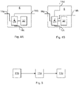
- Figs 2A-B are schematic diagrams illustrating the structure of converter arms 1 of the converter device 8 of Fig 1 according to two embodiments with varying connectivity options to one or more main controllers.
- the converter arm 1 can be any one of the converter arms 1a-f shown in Fig 1 .
- First, the structure of the converter arm shown in Fig 2A will be described.
- the converter arm 1 comprises a plurality of converter cells 6a-6z.
- Two converter cells 6a, 6y are connected to a first main controller 10a and two converter cells 6b, 6z are connected to a second main controller 10b.
- the two main controllers 10a-b are redundant and operate in the same way, with one main controller being active and one main controller being in hot standby.
- the main controller in hot standby is able to step in and quickly take over control if needed, e.g. due to a failing active main controller.
- Each converter cell 6a-z comprises a switching cell with semiconductor switches and an energy storage element, as will be explained in more detail below. Furthermore, at least some of the converter cells 6a-z comprise at least three signal connections, where a signal provided on any one of the signal connections controls the conducting state of the semiconductor switches of the converter cell.
- the signal connections are bidirectional connections.
- Each converter cell 6a-z is connected to receive a signal from either one of the neighbouring entities. Neighbouring is here to be interpreted as adjacent with a direct signal connection.
- a first converter cell 6a has two neighbouring converter cells: a second converter cell 6b and a third converter cell 6c. Moreover, the first converter cell 6a is directly connected to the first main controller 10a.
- At least two of the three entities for each converter cell are neighbouring converter cells. See for example converter cells 6a-b and 6y-z which are respectively connected to two neighbouring converter cells and one of the main controllers 10a-b. Other converter cells are connected to three neighbouring converter cells, see e.g. converter cells 6c-f. More particularly, for instance the third converter cell 6c has three, and only three, neighbouring converter cell: the first converter cell 6a, a fourth converter cell 6d and a fifth converter cell 6e.
- each one of the converter cells 6a-z is arranged to forward a received signal to all connected neighbouring converter cells (and the main controllers 10a-b, if connected to one of the signal connections).
- each converter cell 6a-z can forward signals originating a main controller destined for a converter cell and vice versa.
- Each converter cell is configured to perform this action of signal forwarding autonomously, without additional external control. This forwarding is only performed under the condition that the signal has not been received before. In order for this condition to be evaluated, an identity of each received signal is stored and when a signal is received, its identity is checked against the list of already received signals. The forwarding of the signal then only occurs if the most recently received signal has not been received before.
- a node identity of the originating node of the message is included in the message. This node identity is then stored by the first node, for the time to live period, and any signal with the same originating node is considered to be the same message, and thus considered to have been received before. After the time to live period expires, the node identity is removed or indicated to be inactive.
- each signal does not need to have its own identity; it is sufficient that the originating node is included in the signal.
- a certain indicator in a signal can reset the time-to-live time, i.e. make a specific entry of an originating node immediately inactive.
- each message has its own signal identity. This signal identity is then stored and any signal with the same signal identity is considered to be the same message.
- a signal from the main controllers 10a-b floods the converter cells 6a-z of the converter arm with the signal.
- this arrangement provides great redundancy and resistance to any faults which may affect one or more of the converter cells, even though the main controllers 10a-b only needs to be connected on two sides of the converter cells, with two converter cells connected to the main controllers 10a-b on either side. That is, four converter cells 6a-b, 6y-z are connected to the main controllers 10a-b.
- the redundant two main controllers 10a-b are directly connected to the converter arm 1, to four converter cells 6a-b, 6y-z.
- Fig 2B The embodiment illustrated in Fig 2B is similar to the embodiment illustrated in Fig 2A .
- This embodiment provides a simpler and less expensive solution compared to the embodiment of Fig 2A .
- Fig 3A-B are schematic diagrams illustrating structures of a converter arm of the converter device of Fig 1 according to two embodiments. These embodiment is similar to the embodiment of Figs 2A-B , but also comprising shortcut connections 15a-b. First, the embodiment of Fig 3A will be described.
- a first shortcut connection 15a is provided between a first converter cell 6c and a second converter cell 6y.
- the first and second converter cells 6c,y are not neighbouring converter cells.
- a second shortcut connection 15b is provided between a third converter cell 6b and a fourth converter cell 6x. Also here, in order to make the shortcut connection 15b a shortcut, the third and fourth converter cells 6b,x are not neighbouring converter cells.
- shortcut connections can be placed between any two converter cells.
- the converter cells connected to the shortcut connections 15a-b treat the signal connection just like any other of the signal connections and receive and/or forward signals on this input in the same way as for the other signal connections.
- shortcuts 15a-b Using the shortcuts 15a-b, and since there is a small delay introduced for each time a signal passes through a control cell, the maximum delay for a signal to be propagated from one of the main controllers 10a-b to all converter cells is reduced. This can be particularly useful e.g. for blocking messages. Optionally, more shortcut connections can be provided to further reduce the maximum delay for the signal propagation.
- All converter cells connected to a shortcut connection 15a-b have an additional signal connection, and thus have (at least) four signal inputs.
- Fig 3B this is similar to the embodiment shown in Fig 3A , but there are here two arm controllers 12a-b, which control switching in the converter arm 1, based on signals from the main controllers 10a-b.
- the converter cells 6a-z are all controllable from either one of the main controllers 10a-b as well as either one of the arm controllers 12a-b.
- the arm controllers 12a-b could also be applied for other embodiments, such as those depicted in Figs 2A-B and described above, where the arm controllers would be provided between the main controller(s) and the converter cells.
- Fig 4A-B are schematic diagrams illustrating the structure of two embodiments of a converter cell 6 of Figs 2A-B or Figs 3A-B .
- Fig 4A shows one embodiment of a converter cell 6 that can be any one of the converter cells of Figs 2A-B and any one of the converter cells of Figs 3A-B which are not connected to a shortcut connection, i.e. a converter cell with three signal connections.
- the converter cell 6 comprises a cell controller 2 and a switching cell 32.
- the cell controller 2 is connected to three signal connections 14a-c, to receive and/or forward signals to neighbouring converter cells and/or a main controller, as described above.
- Each signal connection 14a-c can for example be configured to send and/or receive signals using an optical fibre, e.g. using EtherCAT, or any other suitable communication protocol.
- the cell controller 2 When a signal is received on any one of the signal connections 14a-c, the cell controller 2 forwards the signal to the switching cell 32 and to all other signal connections (other than the signal connection over which the signal was received), as long as the signal has not been received before. In this way, any input signal is flooded to all signal connections.
- Fig 4B is illustrates another embodiment of a converter cell 6 that can be any one of the converter cells of Figs 3A-B which is connected to a shortcut connection, i.e. a converter cell with four signal connections.
- the converter cell 6 in this embodiment is similar to the controller cell in the embodiment of Fig 4A .
- Fig 5 is a schematic diagram illustrating communication of time references between nodes of the converter device.
- Each one of the nodes 11a-c can be any node in the converter device 8 described above.
- the nodes can be any one of the converter cells, the arm controllers or the main controllers 10a-b.
- the perspective is from a first node 11a, which receives a time reference from a second node 11b.
- the first node 11a supplies a time reference to a third node 11c, based on the received time reference.
- the second node 11b and the third node 11c can act like the first node in another context.
- the nodes 11a-c can be any nodes in the converter device. Examples of nodes are main controllers, arm controllers and converter cells. Time references can thus e.g. be communicated from a main controller to an arm controller, from a main controller to a converter cell, from a main controller to another main controller, from an arm controller to a converter cell, and from a converter cell to a converter cell.
- Fig 6 is a flow chart illustrating for synchronising time between a plurality of nodes in a converter device. The method is performed in a first node of the converter device, see e.g. the first node 11a of Fig 5 .
- a receive time reference step 40 the first node receives a time reference from a second node.
- a master clock source upon which a plurality of time references in the converter device is based.
- all time references in the converter device can be based on the master clock source. In this way, all of these clocks will be synchronised when each node (except the source node of the master clock source) performs this method.
- the master clock source can e.g. be one of the main controllers.
- the first node obtains a delay value for receiving time references from the second node.
- the delay value can consider both a communication delay and a processing delay.
- the processing delay can relate to the second node, the first node or both nodes.
- the delay value can be e.g. based on measuring a the time of transmitting a signal to a neighbour node and receiving a response.
- the first node determines a compensated time by adding the delay value to the time reference.
- a set clock step 46 the first node sets a clock in the first node to be the compensated time.
- the first node sends the compensated time as a time reference to a third node.
- the hop counter is increased by one.
- this step is only performed if the hop counter is less than a predetermined value. In this way, there is a defined end to forwarding of time references between nodes in the converter device.
- each instance of received time reference has an identifier, in which case this step is only performed if the received time reference has not been received previously.
- the first node sends a confirmation message that the time has been set, as a response to the node from which the time reference was received.
- this signal is forwarded, as described above, through the converter device for all nodes, the main controller can keep track of all the nodes having an up-to-date time setting.
- the compensated time can form a time reference for any downstream nodes. In this way, each node will have a synchronised time, regardless of the number of hops from the original source of the reference time.
- Fig 7 is a schematic diagram illustrating components of any one of the nodes of Fig 5 according to one embodiment. It is to be noted that one or more of the mentioned components can be shared with other functions of the node.
- a processor 60 is provided using any combination of one or more of a suitable central processing unit (CPU), multiprocessor, microcontroller, digital signal processor (DSP), etc., capable of executing software instructions 67 stored in a memory 64, which can thus be a computer program product.
- the processor 60 could alternatively be implemented using an application specific integrated circuit (ASIC), field programmable gate array (FPGA), etc.
- the processor 60 can be configured to execute the method described with reference to Fig 6 above.
- the memory 64 can be any combination of random access memory (RAM) and/or read only memory (ROM).
- the memory 64 also comprises persistent storage, which, for example, can be any single one or combination of magnetic memory, optical memory, solid-state memory or even remotely mounted memory.
- a data memory 66 is also provided for reading and/or storing data during execution of software instructions in the processor 60.
- the data memory 66 can be any combination of RAM and/or ROM.
- the node 11 further comprises an I/O interface 62 for communicating with external and/or internal entities.
- the I/O interface 62 also includes a user interface.
- Fig 8 shows one example of a computer program product comprising computer readable means.
- a computer program 91 can be stored, which computer program can cause a processor to execute a method according to embodiments described herein.
- the computer program product is an optical disc, such as a CD (compact disc) or a DVD (digital versatile disc) or a Blu-Ray disc.
- the computer program product could also be embodied in a memory of a device, such as the computer program product 91 of Fig 7 .
- the computer program 91 is here schematically shown as a track on the depicted optical disk, the computer program can be stored in any way which is suitable for the computer program product, such as a removable solid state memory, e.g. a Universal Serial Bus (USB) drive.
- USB Universal Serial Bus
- Figs 9A-B are schematic diagrams illustrating embodiments of switching cells 32 of the converter cells of Figs 4A-B .
- a switching cell 32 is a combination of one or more semiconductor switches, such as transistors, and one or more energy storing elements, such as capacitors, supercapacitors, inductors, batteries, etc.
- a switching cell can be a multilevel converter structure such as a flying capacitor or MPC (Multi-Point-Clamped) or ANPC (Active - Neutral-Point-Clamped) multilevel structure.
- a gate unit is provided for each semiconductor switch to condition an input signal to a format suitable and/or optimal for the connected semiconductor switch.
- Fig 9A illustrates a switching cell 32 implementing a half bridge structure.
- the switching cell 32 here comprises a leg of two serially connected active components in the form of switches 40a-b, e.g. IGBTs (Insulated-Gate Bipolar Transistors), IGCTs (Insulated Gate-Commutated Thyristors), GTOs (Gate Turn-Off thyristors), etc.
- a leg of two serially connected diodes 42a-b is connected with the leg of serially connected switches 40a-b as shown in the figure, in effect in parallel with the two switches 40a-b.
- An energy storage component 41 is also provided in parallel with the leg of transistors 40a-b and with the leg of diodes 32a-b.
- the voltage synthesized by the switching cell can thus either be zero or the voltage of the energy storage component 41.
- Fig 9B illustrates a switching cell 32 implementing a full bridge structure.
- the switching cell 32 here comprises four switches 40a-d, e.g. IGBTs, IGCTs, GTOs, etc.
- An energy storage component 41 is also provided in parallel across a first leg of two transistors 40a-b and a second leg of two transistors 40c-d.
- the full bridge structure allows the synthesis of a voltage capable of assuming both signs, whereby the voltage of the switching cell can either be zero, the voltage of the energy storage component 41, or a reversed voltage of the energy storage component 41.
- Respective diodes 42a-d are provided in parallel with the switches 40a-d, e.g. in an antiparallel fashion.
- a switch with a parallel diode can be provided together, e.g. using a Reverse Conducting (RC) IGBT, RC-IGCT or BiGT (Bi-mode Insulated Gate Transistor).
- RC Reverse Conducting
- RC-IGCT Reverse Conducting
- BiGT Bi-mode Insulated Gate Transistor
- switching cell 32 is exemplified in Figs 9A-B using a half bridge cell and a full bridge switching cell, the embodiments presented herein are not limited to these examples and are applicable with any suitable configuration of a switching cell.
Description
- The present disclosure relates to the field of converter devices and in particular to communication between different nodes in a converter device.
- High Voltage Direct Current (HVDC) is increasing in usage due to a number of benefits compared to AC (Alternating Current) for power transmission. In order to connect a HVDC link or an HVDC grid to an AC grid, conversion needs to occur from DC (Direct Current) to AC or AC to DC. This conversion can for example be performed using a converter device such as a voltage source converter (VSC).
- In such converter devices, converter cells are controlled by a main controller to synthesize the conversion. When there are many converter cells, each converter cell needs to be able to receive a signal from the main controller, which can get complicated when the number of converter cells is large. Moreover, time needs to be synchronised between different nodes of the converter device.
- A field bus protocol based on the IEEE 802.3 Ethernet standard is proposed by Rietmann Stefan et al. ("Field Bus for Data Exchange and Control of Modular Power Electronic Systems with High Synchronisation Accuracy",2018 IPEC-NIIGATA, IEEJ INDUSTRY APPLICATION SOCIETY, 20 May 2018, pages 2301-2308, XP033428522).
-
EP 2 897 268 A1 - However, the presented time synchronisation is dependent on a known communication path to be able to estimate the delay from the control system to each slave device. When there are multiple redundant communication paths for signals, the presented time synchronisation method is not applicable since the delay can vary depending on the communication path.
- One objective is to provide an improved time synchronisation in a converter device which is applicable when multiple communication paths can be taken.
- According to a first aspect, it is provided a method for synchronising time between a plurality of nodes of a converter device for high voltage power conversion. The method is performed in a first node of the converter device and comprises the steps of: receiving a time reference from a second node; obtaining a delay value for receiving time references from the second node; determining a compensated time by adding the delay value to the time reference; and setting a clock in the first node to be the compensated time.
- The method further comprises the step of: sending the compensated time as a time reference to a third node.
- The delay value may consider both a communication delay and a processing delay.
- There may be a master clock source upon which a plurality of time references in the converter device is based.
- All time references in the converter device may be based on the master clock source.
- According to a second aspect, it is provided a first node for synchronising time between a plurality of nodes of a converter device for high voltage power conversion, the plurality of nodes comprising the first node. The first node comprises: a processor; and a memory storing instructions that, when executed by the processor, cause the first node to: receive a time reference from a second node; obtain a delay value for receiving time references from the second node; determine a compensated time by adding the delay value to the time reference; and set a clock in the first node to be the compensated time.
- The first node further comprises the step of: sending the compensated time as a time reference to a third node.
- The delay value may consider both a communication delay and a processing delay.
- There may be a master clock source upon which a plurality of time references in the converter device is based.
- All time references in the converter device may be based on the master clock source.
- According to a third aspect, it is provided a computer program for synchronising time between a plurality of nodes of a converter device for high voltage power conversion, the plurality of nodes comprising a first node. The computer program comprises computer program code which, when run on the first node causes the first node to: receive a time reference from a second node; obtain a delay value for receiving time references from the second node; determine a compensated time by adding the delay value to the time reference; and set a clock in the first node to be the compensated time.
- According to a fourth aspect, it is provided a computer program product comprising a computer program according to the second aspect and a computer readable means on which the computer program is stored.
- According to a fifth aspect, it is provided a converter arm for power conversion comprising: a plurality of converter cells, wherein at least one of the converter cells comprises a plurality of semiconductor switches, an energy storage element and at least three signal connections arranged to control the conducting state of the plurality of semiconductor switches. At least one converter cell may be connected to receive a signal from at least three entities via said signal connections, wherein at least two of the three entities are neighbouring converter cells, and each converter cell is arranged to forward, as long as the signal has not been received before, a signal to all connected neighbouring converter cells via said signal connections.
- The converter arm may further comprise a shortcut connection between two non-neighbouring converter cells wherein the non neighbouring converter cells each comprises at least four signal connections.
- Each converter cell may be arranged to detect a blocking message supplied to the signal connections separately from other messages supplied to the signal connections, wherein the blocking message instructs the converter cell to turn off all semiconductor switches of the converter cell.
- Each converter cell may be arranged to detect and forward the blocking message without fully decoding a signal comprising the blocking message.
- Four of the converter cells may be directly connected to a main controller, arranged to generate signals arranged to control the conducting state of the plurality of semiconductor switches of the converter cells.
- The converter cells directly connected to the main controller may be connected to only two neighbouring converter cells, and any converter cells not directly connected to the main controller are connected to three neighbouring converter cells.
- Each converter cell may comprise a cell controller and the signal connections of each converter cell are connected to the cell controller, wherein the cell controller is arranged to control the semiconductor switches of the converter cell via respective gate units arranged to condition signals for the semiconductor switches to a suitable format.
- Each converter cell may comprise an auxiliary power input, wherein each auxiliary power input is arranged to power control functions of the respective converter cell without charging the energy storage element of the respective converter cell.
- The converter arm may further comprise at least one battery connected to the auxiliary power inputs of the converter cells.
- Each converter cell may comprise a battery connected to its auxiliary power input.
- Each one of the signal connections may be a bidirectional connection.
- Each one of the signal connections may be arranged to communicate via optical connections.
- According to a sixth aspect, it is provided converter device for converting power in at least one direction between an alternating current, AC, and a direct current, DC, comprising at least one converter arm according to the fifth aspect.
- The converter device may comprise a plurality of phase legs connected in parallel between terminals of a DC connection, and each phase leg comprises at least one converter arm according to the fifth aspect.
- Generally, all terms used in the claims are to be interpreted according to their ordinary meaning in the technical field, unless explicitly defined otherwise herein. All references to "a/an/the element, apparatus, component, means, step, etc." are to be interpreted openly as referring to at least one instance of the element, apparatus, component, means, step, etc., unless explicitly stated otherwise. The steps of any method disclosed herein do not have to be performed in the exact order disclosed, unless explicitly stated.
- Aspects and embodiments are now described, by way of example, with reference to the accompanying drawings, in which:
-
Fig 1 is a schematic diagram illustrating one embodiment of a converter device for converting between DC and AC; -
Figs 2A-B are schematic diagrams illustrating the structure of converter arms of the converter device ofFig 1 according to two embodiments with varying connectivity options to the main controller; -
Fig 3A-B are schematic diagrams illustrating structures of a converter arm of the converter device ofFig 1 according to two embodiments; -
Fig 4A-B are schematic diagrams illustrating the structure of two embodiments of a converter cell ofFigs 2A-B orFig 3 ; -
Fig 5 is a schematic diagram illustrating communication of time references between nodes of the converter device; -
Fig 6 is a flow chart illustrating for synchronising time between a plurality of nodes in a converter device; -
Fig 7 is a schematic diagram illustrating components of any one of the nodes ofFig 5 according to one embodiment; -
Fig 8 shows one example of a computer program product comprising computer readable means; and -
Figs 9A-B are schematic diagrams illustrating embodiments of switching cells of the converter cells ofFigs 4A-B . - The aspects of the present disclosure will now be described more fully hereinafter with reference to the accompanying drawings, in which certain embodiments of the invention are shown. These aspects may, however, be embodied in many different forms and should not be construed as limiting; rather, these embodiments are provided by way of example so that this disclosure will be thorough and complete, and to fully convey the scope of all aspects of invention to those skilled in the art. Like numbers refer to like elements throughout the description.
-
Fig 1 is a schematic diagram illustrating one embodiment of aconverter device 8 for converting between DC and AC. The DC connection comprises a positive terminal DC+ and a negative terminal DC- and can be an HVDC connection. The AC connection in this embodiment is a three phase connection comprising three AC connections ACa, ACb and ACc and can be connected e.g. to an AC grid. While theconverter device 8 is here shown with three phases, theconverter device 8 can equally well have one, two, four or more phases. - Since there are three phases here, there are three
phase legs 7a-c. The threephase legs 7a-c are connected in parallel between terminals DC+, DC- of the DC connection. In this embodiment, afirst phase leg 7a comprises afirst converter arm 1a, afirst inductor 9a, a second inductor, 9b and asecond converter arm 1b connected serially between the terminals DC+, DC- of the DC connection. Analogously, asecond phase leg 7b comprises athird converter arm 1c, athird inductor 9c, a fourth inductor, 9d and afourth converter arm 1d connected serially between the terminals DC+, DC- of the DC connection, and athird phase leg 7c comprises afifth converter arm 1e, afifth inductor 9e, a sixth inductor, 9f and asixth converter arm 1f connected serially between the terminals DC+, DC- of the DC connection. The AC terminals ACa, ACb and ACc are provided between theinductors 9a-b of therespective phase legs 7a-c. Optionally, only one inductor is provided in eachphase leg 7a-c. - A
main controller 10 is connected to allconverter arms 1a-f and sends signals to control the operation of theconverter arms 1a-f. In this way, themain controller 10 controls the operation of the converter arms for conversion from AC to DC or from DC to AC. Additionally, the converter cells in the converter arms can send signals to themain controller 10, e.g. containing measurements, other operational data or any other suitable data. Theconverter device 8 can be unidirectional in either direction between AC and DC or bidirectional. Theconverter device 8 in this embodiment is a voltage source converter. One signal type that can be sent from themain controller 10 to one or more of theconverter arms 1a-f is a blocking message. - While the
converter device 8 is here shown with two converter arms for each phase leg, each phase could comprise any suitable number (1, 2, 3, etc.) of serially connected converter arms, controller by themain controller 10. In particular, if there is a large number of converter cells needed for a phase leg, the phase leg can comprise more than two converter arms. -
Figs 2A-B are schematic diagrams illustrating the structure ofconverter arms 1 of theconverter device 8 ofFig 1 according to two embodiments with varying connectivity options to one or more main controllers. Theconverter arm 1 can be any one of theconverter arms 1a-f shown inFig 1 . First, the structure of the converter arm shown inFig 2A will be described. - The
converter arm 1 comprises a plurality ofconverter cells 6a-6z. Twoconverter cells main controller 10a and twoconverter cells main controller 10b. The twomain controllers 10a-b are redundant and operate in the same way, with one main controller being active and one main controller being in hot standby. The main controller in hot standby is able to step in and quickly take over control if needed, e.g. due to a failing active main controller. - The number of converter cells in the converter arm can vary greatly from installation to installation and can e.g. reach hundreds of converter cells. Each
converter cell 6a-z comprises a switching cell with semiconductor switches and an energy storage element, as will be explained in more detail below. Furthermore, at least some of theconverter cells 6a-z comprise at least three signal connections, where a signal provided on any one of the signal connections controls the conducting state of the semiconductor switches of the converter cell. The signal connections are bidirectional connections. - Each
converter cell 6a-z is connected to receive a signal from either one of the neighbouring entities. Neighbouring is here to be interpreted as adjacent with a direct signal connection. For example, afirst converter cell 6a has two neighbouring converter cells: asecond converter cell 6b and athird converter cell 6c. Moreover, thefirst converter cell 6a is directly connected to the firstmain controller 10a. - As shown in
Fig 2A , at least two of the three entities for each converter cell are neighbouring converter cells. See forexample converter cells 6a-b and 6y-z which are respectively connected to two neighbouring converter cells and one of themain controllers 10a-b. Other converter cells are connected to three neighbouring converter cells, seee.g. converter cells 6c-f. More particularly, for instance thethird converter cell 6c has three, and only three, neighbouring converter cell: thefirst converter cell 6a, afourth converter cell 6d and afifth converter cell 6e. - Furthermore, each one of the
converter cells 6a-z is arranged to forward a received signal to all connected neighbouring converter cells (and themain controllers 10a-b, if connected to one of the signal connections). In other words, eachconverter cell 6a-z can forward signals originating a main controller destined for a converter cell and vice versa. Each converter cell is configured to perform this action of signal forwarding autonomously, without additional external control. This forwarding is only performed under the condition that the signal has not been received before. In order for this condition to be evaluated, an identity of each received signal is stored and when a signal is received, its identity is checked against the list of already received signals. The forwarding of the signal then only occurs if the most recently received signal has not been received before. - The determination of when the signal has been received before can occur in different ways. In one embodiment, a node identity of the originating node of the message is included in the message. This node identity is then stored by the first node, for the time to live period, and any signal with the same originating node is considered to be the same message, and thus considered to have been received before. After the time to live period expires, the node identity is removed or indicated to be inactive. In this embodiment, each signal does not need to have its own identity; it is sufficient that the originating node is included in the signal. Optionally, a certain indicator in a signal can reset the time-to-live time, i.e. make a specific entry of an originating node immediately inactive.
- In one embodiment, each message has its own signal identity. This signal identity is then stored and any signal with the same signal identity is considered to be the same message.
- By only forwarding signals which have not been received before, it is prevented that the same signal continues to be forwarded between nodes in the converter device which, in a worst case scenario, can create an endless loop of signal forwarding of the same signal. The risk for such a loop depends on the topology of nodes in the converter device.
- In this way, a signal from the
main controllers 10a-b floods theconverter cells 6a-z of the converter arm with the signal. Significantly, this arrangement provides great redundancy and resistance to any faults which may affect one or more of the converter cells, even though themain controllers 10a-b only needs to be connected on two sides of the converter cells, with two converter cells connected to themain controllers 10a-b on either side. That is, fourconverter cells 6a-b, 6y-z are connected to themain controllers 10a-b. - Say, for example, that a
first converter cell 6a fails and then anotherconverter cell 6f fails. In systems of the prior art, a failure of two converter cells can affect the controllability of many other converter cells. In contrast, with this arrangement, two failed cells can never affect the controllability of any other cells. In fact, in most cases, three or more converter cells can fail without affecting the controllability of other cells. In the prior art, the only way to reach such resilience to errors is by providing a connection between each individual converter cell and a main controller, which is a costly solution if the number of converter cells is high. - In the structure of
Fig 2A , the redundant twomain controllers 10a-b are directly connected to theconverter arm 1, to fourconverter cells 6a-b, 6y-z. - The embodiment illustrated in
Fig 2B is similar to the embodiment illustrated inFig 2A . Here, however, there is a singlemain controller 10 with four individual connections from the main controller to the four connections to theconnected converter cells 6a-b, 6y-z. This embodiment provides a simpler and less expensive solution compared to the embodiment ofFig 2A . -
Fig 3A-B are schematic diagrams illustrating structures of a converter arm of the converter device ofFig 1 according to two embodiments. These embodiment is similar to the embodiment ofFigs 2A-B , but also comprisingshortcut connections 15a-b. First, the embodiment ofFig 3A will be described. - A
first shortcut connection 15a is provided between afirst converter cell 6c and asecond converter cell 6y. In order to make theshortcut connection 15a a shortcut, the first andsecond converter cells 6c,y are not neighbouring converter cells. - Optionally, a
second shortcut connection 15b is provided between athird converter cell 6b and afourth converter cell 6x. Also here, in order to make theshortcut connection 15b a shortcut, the third andfourth converter cells 6b,x are not neighbouring converter cells. - It is to be noted that shortcut connections can be placed between any two converter cells.
- The converter cells connected to the
shortcut connections 15a-b treat the signal connection just like any other of the signal connections and receive and/or forward signals on this input in the same way as for the other signal connections. - Using the
shortcuts 15a-b, and since there is a small delay introduced for each time a signal passes through a control cell, the maximum delay for a signal to be propagated from one of themain controllers 10a-b to all converter cells is reduced. This can be particularly useful e.g. for blocking messages. Optionally, more shortcut connections can be provided to further reduce the maximum delay for the signal propagation. - All converter cells connected to a
shortcut connection 15a-b have an additional signal connection, and thus have (at least) four signal inputs. - Looking now to
Fig 3B , this is similar to the embodiment shown inFig 3A , but there are here twoarm controllers 12a-b, which control switching in theconverter arm 1, based on signals from themain controllers 10a-b. In this embodiment, there is redundancy in themain controllers 10a-b as well as thearm controllers 12a-b. Theconverter cells 6a-z are all controllable from either one of themain controllers 10a-b as well as either one of thearm controllers 12a-b. Thearm controllers 12a-b could also be applied for other embodiments, such as those depicted inFigs 2A-B and described above, where the arm controllers would be provided between the main controller(s) and the converter cells. -
Fig 4A-B are schematic diagrams illustrating the structure of two embodiments of aconverter cell 6 ofFigs 2A-B orFigs 3A-B .Fig 4A shows one embodiment of aconverter cell 6 that can be any one of the converter cells ofFigs 2A-B and any one of the converter cells ofFigs 3A-B which are not connected to a shortcut connection, i.e. a converter cell with three signal connections. - The
converter cell 6 comprises acell controller 2 and a switchingcell 32. Thecell controller 2 is connected to threesignal connections 14a-c, to receive and/or forward signals to neighbouring converter cells and/or a main controller, as described above. Eachsignal connection 14a-c can for example be configured to send and/or receive signals using an optical fibre, e.g. using EtherCAT, or any other suitable communication protocol. - When a signal is received on any one of the
signal connections 14a-c, thecell controller 2 forwards the signal to the switchingcell 32 and to all other signal connections (other than the signal connection over which the signal was received), as long as the signal has not been received before. In this way, any input signal is flooded to all signal connections. -
Fig 4B is illustrates another embodiment of aconverter cell 6 that can be any one of the converter cells ofFigs 3A-B which is connected to a shortcut connection, i.e. a converter cell with four signal connections. Theconverter cell 6 in this embodiment is similar to the controller cell in the embodiment ofFig 4A . In this embodiment though, there are foursignal connections 14a-d, to be able to accommodate also a signal connection over a shortcut connection. -
Fig 5 is a schematic diagram illustrating communication of time references between nodes of the converter device. Each one of thenodes 11a-c can be any node in theconverter device 8 described above. For instance, the nodes can be any one of the converter cells, the arm controllers or themain controllers 10a-b. - In this figure, the perspective is from a
first node 11a, which receives a time reference from asecond node 11b. Thefirst node 11a, in turn, supplies a time reference to athird node 11c, based on the received time reference. It is to be noted that thesecond node 11b and thethird node 11c can act like the first node in another context. - The
nodes 11a-c can be any nodes in the converter device. Examples of nodes are main controllers, arm controllers and converter cells. Time references can thus e.g. be communicated from a main controller to an arm controller, from a main controller to a converter cell, from a main controller to another main controller, from an arm controller to a converter cell, and from a converter cell to a converter cell. - The time references mentioned here are transmitted using the signals described above.
-
Fig 6 is a flow chart illustrating for synchronising time between a plurality of nodes in a converter device. The method is performed in a first node of the converter device, see e.g. thefirst node 11a ofFig 5 . - In a receive
time reference step 40, the first node receives a time reference from a second node. In the converter device, there is a master clock source upon which a plurality of time references in the converter device is based. In fact, all time references in the converter device can be based on the master clock source. In this way, all of these clocks will be synchronised when each node (except the source node of the master clock source) performs this method. The master clock source can e.g. be one of the main controllers. - In an obtain
delay value step 42, the first node obtains a delay value for receiving time references from the second node. The delay value can consider both a communication delay and a processing delay. The processing delay can relate to the second node, the first node or both nodes. The delay value can be e.g. based on measuring a the time of transmitting a signal to a neighbour node and receiving a response. - In a determine compensated
time step 44, the first node determines a compensated time by adding the delay value to the time reference. - In a
set clock step 46, the first node sets a clock in the first node to be the compensated time. - In
send time step 48, the first node sends the compensated time as a time reference to a third node. Optionally, there is a hop counter in the received time reference. In the time reference sent in this step, the hop counter is increased by one. Optionally, this step is only performed if the hop counter is less than a predetermined value. In this way, there is a defined end to forwarding of time references between nodes in the converter device. In one embodiment, each instance of received time reference has an identifier, in which case this step is only performed if the received time reference has not been received previously. - Optionally, the first node sends a confirmation message that the time has been set, as a response to the node from which the time reference was received. When this signal is forwarded, as described above, through the converter device for all nodes, the main controller can keep track of all the nodes having an up-to-date time setting.
- By adding the delay value to the reference time in the node itself, the compensated time can form a time reference for any downstream nodes. In this way, each node will have a synchronised time, regardless of the number of hops from the original source of the reference time.
-
Fig 7 is a schematic diagram illustrating components of any one of the nodes ofFig 5 according to one embodiment. It is to be noted that one or more of the mentioned components can be shared with other functions of the node. Aprocessor 60 is provided using any combination of one or more of a suitable central processing unit (CPU), multiprocessor, microcontroller, digital signal processor (DSP), etc., capable of executingsoftware instructions 67 stored in amemory 64, which can thus be a computer program product. Theprocessor 60 could alternatively be implemented using an application specific integrated circuit (ASIC), field programmable gate array (FPGA), etc. Theprocessor 60 can be configured to execute the method described with reference toFig 6 above. - The
memory 64 can be any combination of random access memory (RAM) and/or read only memory (ROM). Thememory 64 also comprises persistent storage, which, for example, can be any single one or combination of magnetic memory, optical memory, solid-state memory or even remotely mounted memory. - A
data memory 66 is also provided for reading and/or storing data during execution of software instructions in theprocessor 60. Thedata memory 66 can be any combination of RAM and/or ROM. - The node 11 further comprises an I/
O interface 62 for communicating with external and/or internal entities. Optionally, the I/O interface 62 also includes a user interface. - Other components of the node 11 are omitted in order not to obscure the concepts presented herein.
-
Fig 8 shows one example of a computer program product comprising computer readable means. On this computer readable means, acomputer program 91 can be stored, which computer program can cause a processor to execute a method according to embodiments described herein. In this example, the computer program product is an optical disc, such as a CD (compact disc) or a DVD (digital versatile disc) or a Blu-Ray disc. As explained above, the computer program product could also be embodied in a memory of a device, such as thecomputer program product 91 ofFig 7 . While thecomputer program 91 is here schematically shown as a track on the depicted optical disk, the computer program can be stored in any way which is suitable for the computer program product, such as a removable solid state memory, e.g. a Universal Serial Bus (USB) drive. -
Figs 9A-B are schematic diagrams illustrating embodiments of switchingcells 32 of the converter cells ofFigs 4A-B . A switchingcell 32 is a combination of one or more semiconductor switches, such as transistors, and one or more energy storing elements, such as capacitors, supercapacitors, inductors, batteries, etc. Optionally, a switching cell can be a multilevel converter structure such as a flying capacitor or MPC (Multi-Point-Clamped) or ANPC (Active - Neutral-Point-Clamped) multilevel structure. Optionally, a gate unit is provided for each semiconductor switch to condition an input signal to a format suitable and/or optimal for the connected semiconductor switch. -
Fig 9A illustrates a switchingcell 32 implementing a half bridge structure. The switchingcell 32 here comprises a leg of two serially connected active components in the form ofswitches 40a-b, e.g. IGBTs (Insulated-Gate Bipolar Transistors), IGCTs (Insulated Gate-Commutated Thyristors), GTOs (Gate Turn-Off thyristors), etc. A leg of two seriallyconnected diodes 42a-b is connected with the leg of serially connectedswitches 40a-b as shown in the figure, in effect in parallel with the twoswitches 40a-b. Anenergy storage component 41 is also provided in parallel with the leg oftransistors 40a-b and with the leg of diodes 32a-b. The voltage synthesized by the switching cell can thus either be zero or the voltage of theenergy storage component 41. -
Fig 9B illustrates a switchingcell 32 implementing a full bridge structure. The switchingcell 32 here comprises fourswitches 40a-d, e.g. IGBTs, IGCTs, GTOs, etc. Anenergy storage component 41 is also provided in parallel across a first leg of twotransistors 40a-b and a second leg of twotransistors 40c-d. Compared to the half bridge ofFig 9A , the full bridge structure allows the synthesis of a voltage capable of assuming both signs, whereby the voltage of the switching cell can either be zero, the voltage of theenergy storage component 41, or a reversed voltage of theenergy storage component 41.Respective diodes 42a-d are provided in parallel with theswitches 40a-d, e.g. in an antiparallel fashion. - In
Figs 9A-B , a switch with a parallel diode can be provided together, e.g. using a Reverse Conducting (RC) IGBT, RC-IGCT or BiGT (Bi-mode Insulated Gate Transistor). - It is to be noted that while the switching
cell 32 is exemplified inFigs 9A-B using a half bridge cell and a full bridge switching cell, the embodiments presented herein are not limited to these examples and are applicable with any suitable configuration of a switching cell. - The aspects of the present disclosure have mainly been described above with reference to a few embodiments. However, as is readily appreciated by a person skilled in the art, other embodiments than the ones disclosed above are equally possible within the scope of the invention, as defined by the appended patent claims.
Claims (10)
- A method for synchronising time between a plurality of nodes (11a-c) of a converter device (8) for high voltage power conversion, wherein each of the plurality of nodes comprises a processor (60) and a memory (64), the method being performed in a first node (11a) which comprises a power converter cell (6) of the converter device (8) and the method comprising the steps of:receiving (40) a time reference from a second node (11b);obtaining (42) a delay value for receiving time references from the second node (11b);determining (44) a compensated time by adding the delay value to the time reference;setting (46) a clock in the first node to be the compensated time; andsending (48) the compensated time as a time reference to a third node (11c).
- The method according to claim 1, wherein the delay value considers both a communication delay and a processing delay.
- The method according to any one of the preceding claims, wherein there is a master clock source upon which a plurality of time references in the converter device (8) is based.
- The method according to claim 3, wherein all time references in the converter device (8) are based on the master clock source.
- A first node (11a) for synchronising time between a plurality of nodes (11a-c) of a converter device (8) for high voltage power conversion, wherein each of the plurality of nodes comprises a processor (60) and a memory (64), the plurality of nodes comprising the first node (11a) which comprises a power converter cell (6) of the converter device (8), the
memory (64) of the first node storing instructions (67) that, when executed by the processor, enable the first node (11a) to:receive a time reference from a second node (11b);obtain a delay value for receiving time references from the second node (11b);determine a compensated time by adding the delay value to the time reference;set a clock in the first node to be the compensated time; and send(48) the compensated time as a time reference to a third node (11c). - The first node (11a) according to claim 5, wherein the delay value considers both a communication delay and a processing delay.
- The first node (11a) according to claim 5 or 6, wherein there is a master clock source upon which a plurality of time references in the converter device (8) is based.
- The first node (11a) according to claim 7, wherein all time references in the converter device (8) are based on the master clock source.
- A computer program (67, 91) for synchronising time between a plurality of nodes (11a-c) of a converter device (8) for high voltage power conversion, wherein each of the plurality of nodes comprises a processor (60) and a memory (64), the plurality of nodes comprising a first node (11a) which comprises a power converter cell (6) of the converter device (8), the computer program comprising computer program code which, when run on the first node (11a) enables the first node (11a) to:receive a time reference from a second node (11b);obtain a delay value for receiving time references from the second node (11b);determine a compensated time by adding the delay value to the time reference;set a clock in the first node to be the compensated time; andsend the compensated time as a time reference to a third node (11c).
- A computer program product (64, 90) comprising a computer program according to claim 9 and a computer readable means on which the computer program is stored.
Priority Applications (4)
| Application Number | Priority Date | Filing Date | Title |
|---|---|---|---|
| EP19159285.6A EP3703241B1 (en) | 2019-02-26 | 2019-02-26 | Communication in a converter device |
| CN202010100183.XA CN111614426B (en) | 2019-02-26 | 2020-02-18 | Communication in a converter device |
| US16/801,299 US11532940B2 (en) | 2019-02-26 | 2020-02-26 | Communication in a converter device |
| US18/061,744 US20230095300A1 (en) | 2019-02-26 | 2022-12-05 | Communication in a converter device |
Applications Claiming Priority (1)
| Application Number | Priority Date | Filing Date | Title |
|---|---|---|---|
| EP19159285.6A EP3703241B1 (en) | 2019-02-26 | 2019-02-26 | Communication in a converter device |
Publications (2)
| Publication Number | Publication Date |
|---|---|
| EP3703241A1 EP3703241A1 (en) | 2020-09-02 |
| EP3703241B1 true EP3703241B1 (en) | 2022-07-13 |
Family
ID=65598470
Family Applications (1)
| Application Number | Title | Priority Date | Filing Date |
|---|---|---|---|
| EP19159285.6A Active EP3703241B1 (en) | 2019-02-26 | 2019-02-26 | Communication in a converter device |
Country Status (3)
| Country | Link |
|---|---|
| US (2) | US11532940B2 (en) |
| EP (1) | EP3703241B1 (en) |
| CN (1) | CN111614426B (en) |
Families Citing this family (1)
| Publication number | Priority date | Publication date | Assignee | Title |
|---|---|---|---|---|
| CN117378113A (en) * | 2021-04-14 | 2024-01-09 | 日立能源有限公司 | Grid integrated control platform architecture for large-scale grid energy storage systems |
Citations (1)
| Publication number | Priority date | Publication date | Assignee | Title |
|---|---|---|---|---|
| US20140119080A1 (en) * | 2012-10-26 | 2014-05-01 | Kabushiki Kaisha Toshiba | Inverter apparatus and inverter system |
Family Cites Families (33)
| Publication number | Priority date | Publication date | Assignee | Title |
|---|---|---|---|---|
| GB2301991B (en) * | 1995-06-06 | 1999-06-30 | Plessey Telecomm | SDH Network |
| DE19901588A1 (en) * | 1999-01-16 | 2000-07-20 | Alcatel Sa | Synchronization of a network element in a synchronous digital communication network |
| US7103124B1 (en) * | 1999-12-30 | 2006-09-05 | Telefonaktiebolaget Lm Ericsson (Publ) | Synchronization of nodes |
| CN1228908C (en) * | 2001-12-31 | 2005-11-23 | 艾默生网络能源有限公司 | Switch synchronization method of parallel converter system. |
| US7518894B2 (en) * | 2005-03-31 | 2009-04-14 | Silicon Laboratories Inc. | Distributed power supply system having reassignable master |
| KR20090032306A (en) * | 2007-09-27 | 2009-04-01 | 한국전자통신연구원 | Time synchronization system and method on the network |
| US8169856B2 (en) * | 2008-10-24 | 2012-05-01 | Oracle International Corporation | Time synchronization in cluster systems |
| KR101114702B1 (en) * | 2008-12-18 | 2012-02-29 | 삼성전자주식회사 | Method and system for time synchronization among nodes in a wireless communication system |
| CN101510849B (en) * | 2009-03-18 | 2011-05-18 | 中国电信股份有限公司 | Method and equipment for obtaining node transmission information of transmission path |
| JP5449893B2 (en) * | 2009-07-21 | 2014-03-19 | 株式会社日立製作所 | Power converter |
| DE102010022525A1 (en) | 2010-02-11 | 2012-05-10 | Siemens Aktiengesellschaft | Method for time synchronization in communication network for industrial automation system, involves estimating frequency ratio of reference cycle frequency to internal cycle frequency of node |
| EP2506470B1 (en) * | 2011-03-29 | 2013-05-29 | Alcatel Lucent | Method, apparatus and system for time distribution in a telecommunications network |
| US8120935B2 (en) * | 2011-03-29 | 2012-02-21 | American Superconductor Corporation | Power converter with dual ring network control |
| US9106353B2 (en) * | 2011-12-13 | 2015-08-11 | Jds Uniphase Corporation | Time synchronization for network testing equipment |
| US9590411B2 (en) * | 2011-12-15 | 2017-03-07 | Schweitzer Engineering Laboratories, Inc. | Systems and methods for time synchronization of IEDs via radio link |
| CN103188064A (en) * | 2011-12-28 | 2013-07-03 | 中兴通讯股份有限公司 | Clock synchronization method and clock synchronization device |
| US9043040B2 (en) * | 2012-01-31 | 2015-05-26 | General Electric Company | Power system stabilization |
| US9106352B2 (en) * | 2012-02-27 | 2015-08-11 | Telefonaktiebolaget L M Ericsson (Publ) | Frequency distribution using precision time protocol |
| CN104782042B (en) * | 2012-10-01 | 2016-08-17 | Abb技术有限公司 | Converter arm with associate converter apparatus |
| CN103067149A (en) | 2012-12-06 | 2013-04-24 | 国网智能电网研究院 | Rectification method capable of enabling voltage source converter valve to control and command clock synchronously |
| TWI627812B (en) * | 2013-04-05 | 2018-06-21 | 美商線性科技股份有限公司 | Device, system, and method of voltage compensated active cell balancing |
| US20150015072A1 (en) * | 2013-07-12 | 2015-01-15 | Infineon Technologies Austria Ag | Power Converter Circuit and Method |
| US9112631B2 (en) * | 2013-09-11 | 2015-08-18 | Khalifa University of Science, Technology, and Research | Method and devices for frequency distribution |
| EP2897268B1 (en) | 2014-01-20 | 2022-01-05 | ABB Schweiz AG | Master/slave controller system in ring topology for modular multilevel converters |
| US10346910B2 (en) * | 2014-04-16 | 2019-07-09 | Iex Group, Inc. | Systems and methods for providing up-to-date information for transactions |
| KR101596756B1 (en) * | 2014-11-03 | 2016-03-07 | 현대자동차주식회사 | Method and apparatus for providing in-vehicle network time synchronization using redundant GrandMaster |
| DE102015106196B3 (en) * | 2015-04-02 | 2016-06-23 | Rainer Marquardt | Low loss modular multilevel converter |
| WO2016181198A1 (en) * | 2015-05-14 | 2016-11-17 | Telefonaktiebolaget Lm Ericsson (Publ) | Methods and system for synchronizing nodes in a wireless network |
| JP2017098694A (en) * | 2015-11-20 | 2017-06-01 | 富士通株式会社 | Communication apparatus and time synchronizing method therefor |
| US10833840B2 (en) * | 2018-05-07 | 2020-11-10 | ZaiNar, Inc. | Methods for nanosecond-scale time synchronization over a network |
| US10911211B1 (en) * | 2018-09-28 | 2021-02-02 | ZaiNar, Inc. | Frequency and gain calibration for time synchronization in a network |
| WO2020123921A1 (en) * | 2018-12-14 | 2020-06-18 | Cummins Inc. | End of battery state of charge (soc) vehicle system operation |
| JP7230690B2 (en) * | 2019-05-28 | 2023-03-01 | 富士通株式会社 | Time synchronization program, information processing device and time synchronization method |
-
2019
- 2019-02-26 EP EP19159285.6A patent/EP3703241B1/en active Active
-
2020
- 2020-02-18 CN CN202010100183.XA patent/CN111614426B/en active Active
- 2020-02-26 US US16/801,299 patent/US11532940B2/en active Active
-
2022
- 2022-12-05 US US18/061,744 patent/US20230095300A1/en active Pending
Patent Citations (1)
| Publication number | Priority date | Publication date | Assignee | Title |
|---|---|---|---|---|
| US20140119080A1 (en) * | 2012-10-26 | 2014-05-01 | Kabushiki Kaisha Toshiba | Inverter apparatus and inverter system |
Also Published As
| Publication number | Publication date |
|---|---|
| US20230095300A1 (en) | 2023-03-30 |
| CN111614426A (en) | 2020-09-01 |
| US11532940B2 (en) | 2022-12-20 |
| EP3703241A1 (en) | 2020-09-02 |
| CN111614426B (en) | 2023-02-24 |
| US20200274463A1 (en) | 2020-08-27 |
Similar Documents
| Publication | Publication Date | Title |
|---|---|---|
| EP2904698B1 (en) | Converter arm and associated converter device | |
| US11081974B2 (en) | Fault tolerant multilevel modular power conversion device | |
| US20190173313A1 (en) | Isolated parallel ups system with choke bypass switch | |
| JP6412266B2 (en) | Uninterruptible power system | |
| JP2015130746A (en) | Power conversion device and method of controlling the same | |
| Burlacu et al. | Synchronization of the distributed PWM carrier waves for modular multilevel converters | |
| KR20130124772A (en) | System and method for converting electric power, and apparatus and method for controlling the system | |
| US20230095300A1 (en) | Communication in a converter device | |
| JP6425855B1 (en) | Power converter | |
| JP2015115977A (en) | Power conversion equipment | |
| JP2015156740A (en) | Power conversion device | |
| EP3588735B1 (en) | Communication systems and methods in uninterruptible power supply systems | |
| WO2019185418A1 (en) | Converter controller | |
| JP7117818B2 (en) | power converter | |
| EP3731369B1 (en) | Determining a network map defining a structure of a network | |
| WO2020110203A1 (en) | Power conversion device | |
| EP3940936A1 (en) | Electrical converter with bypass function | |
| JP2019088052A (en) | Uninterruptible power supply system | |
| Marquez et al. | Communications scheme of a modular power conversion system | |
| CN117378113A (en) | Grid integrated control platform architecture for large-scale grid energy storage systems |
Legal Events
| Date | Code | Title | Description |
|---|---|---|---|
| PUAI | Public reference made under article 153(3) epc to a published international application that has entered the european phase |
Free format text: ORIGINAL CODE: 0009012 |
|
| STAA | Information on the status of an ep patent application or granted ep patent |
Free format text: STATUS: THE APPLICATION HAS BEEN PUBLISHED |
|
| AK | Designated contracting states |
Kind code of ref document: A1 Designated state(s): AL AT BE BG CH CY CZ DE DK EE ES FI FR GB GR HR HU IE IS IT LI LT LU LV MC MK MT NL NO PL PT RO RS SE SI SK SM TR |
|
| AX | Request for extension of the european patent |
Extension state: BA ME |
|
| STAA | Information on the status of an ep patent application or granted ep patent |
Free format text: STATUS: REQUEST FOR EXAMINATION WAS MADE |
|
| STAA | Information on the status of an ep patent application or granted ep patent |
Free format text: STATUS: EXAMINATION IS IN PROGRESS |
|
| 17P | Request for examination filed |
Effective date: 20210302 |
|
| RBV | Designated contracting states (corrected) |
Designated state(s): AL AT BE BG CH CY CZ DE DK EE ES FI FR GB GR HR HU IE IS IT LI LT LU LV MC MK MT NL NO PL PT RO RS SE SI SK SM TR |
|
| 17Q | First examination report despatched |
Effective date: 20210330 |
|
| RAP3 | Party data changed (applicant data changed or rights of an application transferred) |
Owner name: HITACHI ENERGY SWITZERLAND AG |
|
| GRAP | Despatch of communication of intention to grant a patent |
Free format text: ORIGINAL CODE: EPIDOSNIGR1 |
|
| STAA | Information on the status of an ep patent application or granted ep patent |
Free format text: STATUS: GRANT OF PATENT IS INTENDED |
|
| RIC1 | Information provided on ipc code assigned before grant |
Ipc: H02M 1/00 20060101ALN20220216BHEP Ipc: H02J 3/40 20060101ALI20220216BHEP Ipc: H02M 7/483 20070101AFI20220216BHEP |
|
| INTG | Intention to grant announced |
Effective date: 20220302 |
|
| GRAS | Grant fee paid |
Free format text: ORIGINAL CODE: EPIDOSNIGR3 |
|
| GRAA | (expected) grant |
Free format text: ORIGINAL CODE: 0009210 |
|
| STAA | Information on the status of an ep patent application or granted ep patent |
Free format text: STATUS: THE PATENT HAS BEEN GRANTED |
|
| AK | Designated contracting states |
Kind code of ref document: B1 Designated state(s): AL AT BE BG CH CY CZ DE DK EE ES FI FR GB GR HR HU IE IS IT LI LT LU LV MC MK MT NL NO PL PT RO RS SE SI SK SM TR |
|
| REG | Reference to a national code |
Ref country code: CH Ref legal event code: EP |
|
| REG | Reference to a national code |
Ref country code: DE Ref legal event code: R096 Ref document number: 602019016871 Country of ref document: DE |
|
| REG | Reference to a national code |
Ref country code: AT Ref legal event code: REF Ref document number: 1504786 Country of ref document: AT Kind code of ref document: T Effective date: 20220815 |
|
| REG | Reference to a national code |
Ref country code: IE Ref legal event code: FG4D |
|
| REG | Reference to a national code |
Ref country code: LT Ref legal event code: MG9D |
|
| REG | Reference to a national code |
Ref country code: NL Ref legal event code: MP Effective date: 20220713 |
|
| PG25 | Lapsed in a contracting state [announced via postgrant information from national office to epo] |
Ref country code: SE Free format text: LAPSE BECAUSE OF FAILURE TO SUBMIT A TRANSLATION OF THE DESCRIPTION OR TO PAY THE FEE WITHIN THE PRESCRIBED TIME-LIMIT Effective date: 20220713 Ref country code: RS Free format text: LAPSE BECAUSE OF FAILURE TO SUBMIT A TRANSLATION OF THE DESCRIPTION OR TO PAY THE FEE WITHIN THE PRESCRIBED TIME-LIMIT Effective date: 20220713 Ref country code: PT Free format text: LAPSE BECAUSE OF FAILURE TO SUBMIT A TRANSLATION OF THE DESCRIPTION OR TO PAY THE FEE WITHIN THE PRESCRIBED TIME-LIMIT Effective date: 20221114 Ref country code: NO Free format text: LAPSE BECAUSE OF FAILURE TO SUBMIT A TRANSLATION OF THE DESCRIPTION OR TO PAY THE FEE WITHIN THE PRESCRIBED TIME-LIMIT Effective date: 20221013 Ref country code: NL Free format text: LAPSE BECAUSE OF FAILURE TO SUBMIT A TRANSLATION OF THE DESCRIPTION OR TO PAY THE FEE WITHIN THE PRESCRIBED TIME-LIMIT Effective date: 20220713 Ref country code: LV Free format text: LAPSE BECAUSE OF FAILURE TO SUBMIT A TRANSLATION OF THE DESCRIPTION OR TO PAY THE FEE WITHIN THE PRESCRIBED TIME-LIMIT Effective date: 20220713 Ref country code: LT Free format text: LAPSE BECAUSE OF FAILURE TO SUBMIT A TRANSLATION OF THE DESCRIPTION OR TO PAY THE FEE WITHIN THE PRESCRIBED TIME-LIMIT Effective date: 20220713 Ref country code: FI Free format text: LAPSE BECAUSE OF FAILURE TO SUBMIT A TRANSLATION OF THE DESCRIPTION OR TO PAY THE FEE WITHIN THE PRESCRIBED TIME-LIMIT Effective date: 20220713 Ref country code: ES Free format text: LAPSE BECAUSE OF FAILURE TO SUBMIT A TRANSLATION OF THE DESCRIPTION OR TO PAY THE FEE WITHIN THE PRESCRIBED TIME-LIMIT Effective date: 20220713 |
|
| REG | Reference to a national code |
Ref country code: AT Ref legal event code: MK05 Ref document number: 1504786 Country of ref document: AT Kind code of ref document: T Effective date: 20220713 |
|
| PG25 | Lapsed in a contracting state [announced via postgrant information from national office to epo] |
Ref country code: PL Free format text: LAPSE BECAUSE OF FAILURE TO SUBMIT A TRANSLATION OF THE DESCRIPTION OR TO PAY THE FEE WITHIN THE PRESCRIBED TIME-LIMIT Effective date: 20220713 Ref country code: IS Free format text: LAPSE BECAUSE OF FAILURE TO SUBMIT A TRANSLATION OF THE DESCRIPTION OR TO PAY THE FEE WITHIN THE PRESCRIBED TIME-LIMIT Effective date: 20221113 Ref country code: HR Free format text: LAPSE BECAUSE OF FAILURE TO SUBMIT A TRANSLATION OF THE DESCRIPTION OR TO PAY THE FEE WITHIN THE PRESCRIBED TIME-LIMIT Effective date: 20220713 Ref country code: GR Free format text: LAPSE BECAUSE OF FAILURE TO SUBMIT A TRANSLATION OF THE DESCRIPTION OR TO PAY THE FEE WITHIN THE PRESCRIBED TIME-LIMIT Effective date: 20221014 |
|
| REG | Reference to a national code |
Ref country code: DE Ref legal event code: R097 Ref document number: 602019016871 Country of ref document: DE |
|
| PG25 | Lapsed in a contracting state [announced via postgrant information from national office to epo] |
Ref country code: SM Free format text: LAPSE BECAUSE OF FAILURE TO SUBMIT A TRANSLATION OF THE DESCRIPTION OR TO PAY THE FEE WITHIN THE PRESCRIBED TIME-LIMIT Effective date: 20220713 Ref country code: RO Free format text: LAPSE BECAUSE OF FAILURE TO SUBMIT A TRANSLATION OF THE DESCRIPTION OR TO PAY THE FEE WITHIN THE PRESCRIBED TIME-LIMIT Effective date: 20220713 Ref country code: DK Free format text: LAPSE BECAUSE OF FAILURE TO SUBMIT A TRANSLATION OF THE DESCRIPTION OR TO PAY THE FEE WITHIN THE PRESCRIBED TIME-LIMIT Effective date: 20220713 Ref country code: CZ Free format text: LAPSE BECAUSE OF FAILURE TO SUBMIT A TRANSLATION OF THE DESCRIPTION OR TO PAY THE FEE WITHIN THE PRESCRIBED TIME-LIMIT Effective date: 20220713 Ref country code: AT Free format text: LAPSE BECAUSE OF FAILURE TO SUBMIT A TRANSLATION OF THE DESCRIPTION OR TO PAY THE FEE WITHIN THE PRESCRIBED TIME-LIMIT Effective date: 20220713 |
|
| PGFP | Annual fee paid to national office [announced via postgrant information from national office to epo] |
Ref country code: FR Payment date: 20230221 Year of fee payment: 5 |
|
| PLBE | No opposition filed within time limit |
Free format text: ORIGINAL CODE: 0009261 |
|
| STAA | Information on the status of an ep patent application or granted ep patent |
Free format text: STATUS: NO OPPOSITION FILED WITHIN TIME LIMIT |
|
| PG25 | Lapsed in a contracting state [announced via postgrant information from national office to epo] |
Ref country code: SK Free format text: LAPSE BECAUSE OF FAILURE TO SUBMIT A TRANSLATION OF THE DESCRIPTION OR TO PAY THE FEE WITHIN THE PRESCRIBED TIME-LIMIT Effective date: 20220713 Ref country code: EE Free format text: LAPSE BECAUSE OF FAILURE TO SUBMIT A TRANSLATION OF THE DESCRIPTION OR TO PAY THE FEE WITHIN THE PRESCRIBED TIME-LIMIT Effective date: 20220713 |
|
| PGFP | Annual fee paid to national office [announced via postgrant information from national office to epo] |
Ref country code: GB Payment date: 20230221 Year of fee payment: 5 Ref country code: DE Payment date: 20230216 Year of fee payment: 5 |
|
| 26N | No opposition filed |
Effective date: 20230414 |
|
| PG25 | Lapsed in a contracting state [announced via postgrant information from national office to epo] |
Ref country code: AL Free format text: LAPSE BECAUSE OF FAILURE TO SUBMIT A TRANSLATION OF THE DESCRIPTION OR TO PAY THE FEE WITHIN THE PRESCRIBED TIME-LIMIT Effective date: 20220713 |
|
| P01 | Opt-out of the competence of the unified patent court (upc) registered |
Effective date: 20230527 |
|
| PG25 | Lapsed in a contracting state [announced via postgrant information from national office to epo] |
Ref country code: SI Free format text: LAPSE BECAUSE OF FAILURE TO SUBMIT A TRANSLATION OF THE DESCRIPTION OR TO PAY THE FEE WITHIN THE PRESCRIBED TIME-LIMIT Effective date: 20220713 |
|
| PG25 | Lapsed in a contracting state [announced via postgrant information from national office to epo] |
Ref country code: MC Free format text: LAPSE BECAUSE OF FAILURE TO SUBMIT A TRANSLATION OF THE DESCRIPTION OR TO PAY THE FEE WITHIN THE PRESCRIBED TIME-LIMIT Effective date: 20220713 |
|
| REG | Reference to a national code |
Ref country code: CH Ref legal event code: PL |
|
| REG | Reference to a national code |
Ref country code: BE Ref legal event code: MM Effective date: 20230228 |
|
| PG25 | Lapsed in a contracting state [announced via postgrant information from national office to epo] |
Ref country code: LU Free format text: LAPSE BECAUSE OF NON-PAYMENT OF DUE FEES Effective date: 20230226 Ref country code: LI Free format text: LAPSE BECAUSE OF NON-PAYMENT OF DUE FEES Effective date: 20230228 Ref country code: CH Free format text: LAPSE BECAUSE OF NON-PAYMENT OF DUE FEES Effective date: 20230228 |
|
| REG | Reference to a national code |
Ref country code: IE Ref legal event code: MM4A |
|
| PG25 | Lapsed in a contracting state [announced via postgrant information from national office to epo] |
Ref country code: IT Free format text: LAPSE BECAUSE OF FAILURE TO SUBMIT A TRANSLATION OF THE DESCRIPTION OR TO PAY THE FEE WITHIN THE PRESCRIBED TIME-LIMIT Effective date: 20220713 Ref country code: IE Free format text: LAPSE BECAUSE OF NON-PAYMENT OF DUE FEES Effective date: 20230226 |
|
| PG25 | Lapsed in a contracting state [announced via postgrant information from national office to epo] |
Ref country code: BE Free format text: LAPSE BECAUSE OF NON-PAYMENT OF DUE FEES Effective date: 20230228 |
|
| REG | Reference to a national code |
Ref country code: DE Ref legal event code: R081 Ref document number: 602019016871 Country of ref document: DE Owner name: HITACHI ENERGY LTD, CH Free format text: FORMER OWNER: HITACHI ENERGY SWITZERLAND AG, BADEN, CH |
|
| PGFP | Annual fee paid to national office [announced via postgrant information from national office to epo] |
Ref country code: DE Payment date: 20240219 Year of fee payment: 6 Ref country code: GB Payment date: 20240219 Year of fee payment: 6 |