EP3674098A1 - Ablation blockers - Google Patents
Ablation blockers Download PDFInfo
- Publication number
- EP3674098A1 EP3674098A1 EP19170398.2A EP19170398A EP3674098A1 EP 3674098 A1 EP3674098 A1 EP 3674098A1 EP 19170398 A EP19170398 A EP 19170398A EP 3674098 A1 EP3674098 A1 EP 3674098A1
- Authority
- EP
- European Patent Office
- Prior art keywords
- electromagnetic radiation
- protection structure
- data carrier
- processing
- spectrum
- Prior art date
- Legal status (The legal status is an assumption and is not a legal conclusion. Google has not performed a legal analysis and makes no representation as to the accuracy of the status listed.)
- Withdrawn
Links
- 238000002679 ablation Methods 0.000 title description 11
- 230000005670 electromagnetic radiation Effects 0.000 claims abstract description 105
- 238000001228 spectrum Methods 0.000 claims abstract description 46
- 238000000034 method Methods 0.000 claims abstract description 12
- 239000000976 ink Substances 0.000 claims description 14
- 239000002105 nanoparticle Substances 0.000 claims description 12
- 230000003287 optical effect Effects 0.000 claims description 10
- 239000000654 additive Substances 0.000 claims description 8
- 239000000049 pigment Substances 0.000 claims description 8
- 229920000139 polyethylene terephthalate Polymers 0.000 claims description 7
- 239000005020 polyethylene terephthalate Substances 0.000 claims description 7
- 150000002736 metal compounds Chemical class 0.000 claims description 6
- 239000004033 plastic Substances 0.000 claims description 6
- 229920003023 plastic Polymers 0.000 claims description 6
- 229920000515 polycarbonate Polymers 0.000 claims description 6
- 239000004417 polycarbonate Substances 0.000 claims description 6
- 229910052751 metal Inorganic materials 0.000 claims description 5
- 239000002184 metal Substances 0.000 claims description 5
- -1 polyethylene terephthalate Polymers 0.000 claims description 5
- 150000002739 metals Chemical class 0.000 claims description 4
- 239000000975 dye Substances 0.000 claims description 3
- 239000010410 layer Substances 0.000 description 211
- 230000005855 radiation Effects 0.000 description 45
- 230000004888 barrier function Effects 0.000 description 8
- 230000005540 biological transmission Effects 0.000 description 6
- 238000004519 manufacturing process Methods 0.000 description 6
- 239000000969 carrier Substances 0.000 description 5
- 230000001678 irradiating effect Effects 0.000 description 5
- 239000011159 matrix material Substances 0.000 description 5
- VYPSYNLAJGMNEJ-UHFFFAOYSA-N Silicium dioxide Chemical compound O=[Si]=O VYPSYNLAJGMNEJ-UHFFFAOYSA-N 0.000 description 4
- 238000010521 absorption reaction Methods 0.000 description 4
- 230000000903 blocking effect Effects 0.000 description 3
- 238000010030 laminating Methods 0.000 description 3
- 239000000463 material Substances 0.000 description 3
- 229920000728 polyester Polymers 0.000 description 3
- GWEVSGVZZGPLCZ-UHFFFAOYSA-N Titan oxide Chemical compound O=[Ti]=O GWEVSGVZZGPLCZ-UHFFFAOYSA-N 0.000 description 2
- 238000002835 absorbance Methods 0.000 description 2
- 239000003086 colorant Substances 0.000 description 2
- 238000003475 lamination Methods 0.000 description 2
- 230000001902 propagating effect Effects 0.000 description 2
- 239000000377 silicon dioxide Substances 0.000 description 2
- HWRLEEPNFJNTOP-UHFFFAOYSA-N 2-(1,3,5-triazin-2-yl)phenol Chemical class OC1=CC=CC=C1C1=NC=NC=N1 HWRLEEPNFJNTOP-UHFFFAOYSA-N 0.000 description 1
- OKTJSMMVPCPJKN-UHFFFAOYSA-N Carbon Chemical compound [C] OKTJSMMVPCPJKN-UHFFFAOYSA-N 0.000 description 1
- ATJFFYVFTNAWJD-UHFFFAOYSA-N Tin Chemical compound [Sn] ATJFFYVFTNAWJD-UHFFFAOYSA-N 0.000 description 1
- 230000000996 additive effect Effects 0.000 description 1
- 230000004075 alteration Effects 0.000 description 1
- 229910052782 aluminium Inorganic materials 0.000 description 1
- 239000007844 bleaching agent Substances 0.000 description 1
- 229910052799 carbon Inorganic materials 0.000 description 1
- 229910052802 copper Inorganic materials 0.000 description 1
- 239000013078 crystal Substances 0.000 description 1
- 230000007423 decrease Effects 0.000 description 1
- 229910003460 diamond Inorganic materials 0.000 description 1
- 239000010432 diamond Substances 0.000 description 1
- 230000000694 effects Effects 0.000 description 1
- 238000004049 embossing Methods 0.000 description 1
- 238000001125 extrusion Methods 0.000 description 1
- 239000000835 fiber Substances 0.000 description 1
- 239000000945 filler Substances 0.000 description 1
- 238000001914 filtration Methods 0.000 description 1
- 229910052737 gold Inorganic materials 0.000 description 1
- 238000005286 illumination Methods 0.000 description 1
- 238000010348 incorporation Methods 0.000 description 1
- 238000000608 laser ablation Methods 0.000 description 1
- 230000004048 modification Effects 0.000 description 1
- 238000012986 modification Methods 0.000 description 1
- 238000007645 offset printing Methods 0.000 description 1
- 230000000737 periodic effect Effects 0.000 description 1
- 239000002985 plastic film Substances 0.000 description 1
- 229920005644 polyethylene terephthalate glycol copolymer Polymers 0.000 description 1
- 229920000642 polymer Polymers 0.000 description 1
- 230000002265 prevention Effects 0.000 description 1
- 238000007650 screen-printing Methods 0.000 description 1
- 235000012239 silicon dioxide Nutrition 0.000 description 1
- 229910052709 silver Inorganic materials 0.000 description 1
- 239000002356 single layer Substances 0.000 description 1
- 239000007787 solid Substances 0.000 description 1
- 239000000126 substance Substances 0.000 description 1
- 239000010409 thin film Substances 0.000 description 1
- 239000010936 titanium Substances 0.000 description 1
- 229910052719 titanium Inorganic materials 0.000 description 1
- 239000012780 transparent material Substances 0.000 description 1
Images


Classifications
-
- B—PERFORMING OPERATIONS; TRANSPORTING
- B42—BOOKBINDING; ALBUMS; FILES; SPECIAL PRINTED MATTER
- B42D—BOOKS; BOOK COVERS; LOOSE LEAVES; PRINTED MATTER CHARACTERISED BY IDENTIFICATION OR SECURITY FEATURES; PRINTED MATTER OF SPECIAL FORMAT OR STYLE NOT OTHERWISE PROVIDED FOR; DEVICES FOR USE THEREWITH AND NOT OTHERWISE PROVIDED FOR; MOVABLE-STRIP WRITING OR READING APPARATUS
- B42D25/00—Information-bearing cards or sheet-like structures characterised by identification or security features; Manufacture thereof
- B42D25/20—Information-bearing cards or sheet-like structures characterised by identification or security features; Manufacture thereof characterised by a particular use or purpose
- B42D25/23—Identity cards
-
- B—PERFORMING OPERATIONS; TRANSPORTING
- B42—BOOKBINDING; ALBUMS; FILES; SPECIAL PRINTED MATTER
- B42D—BOOKS; BOOK COVERS; LOOSE LEAVES; PRINTED MATTER CHARACTERISED BY IDENTIFICATION OR SECURITY FEATURES; PRINTED MATTER OF SPECIAL FORMAT OR STYLE NOT OTHERWISE PROVIDED FOR; DEVICES FOR USE THEREWITH AND NOT OTHERWISE PROVIDED FOR; MOVABLE-STRIP WRITING OR READING APPARATUS
- B42D13/00—Loose leaves modified for binding; Inserts
-
- B—PERFORMING OPERATIONS; TRANSPORTING
- B42—BOOKBINDING; ALBUMS; FILES; SPECIAL PRINTED MATTER
- B42D—BOOKS; BOOK COVERS; LOOSE LEAVES; PRINTED MATTER CHARACTERISED BY IDENTIFICATION OR SECURITY FEATURES; PRINTED MATTER OF SPECIAL FORMAT OR STYLE NOT OTHERWISE PROVIDED FOR; DEVICES FOR USE THEREWITH AND NOT OTHERWISE PROVIDED FOR; MOVABLE-STRIP WRITING OR READING APPARATUS
- B42D25/00—Information-bearing cards or sheet-like structures characterised by identification or security features; Manufacture thereof
- B42D25/20—Information-bearing cards or sheet-like structures characterised by identification or security features; Manufacture thereof characterised by a particular use or purpose
- B42D25/24—Passports
-
- B—PERFORMING OPERATIONS; TRANSPORTING
- B42—BOOKBINDING; ALBUMS; FILES; SPECIAL PRINTED MATTER
- B42D—BOOKS; BOOK COVERS; LOOSE LEAVES; PRINTED MATTER CHARACTERISED BY IDENTIFICATION OR SECURITY FEATURES; PRINTED MATTER OF SPECIAL FORMAT OR STYLE NOT OTHERWISE PROVIDED FOR; DEVICES FOR USE THEREWITH AND NOT OTHERWISE PROVIDED FOR; MOVABLE-STRIP WRITING OR READING APPARATUS
- B42D25/00—Information-bearing cards or sheet-like structures characterised by identification or security features; Manufacture thereof
- B42D25/30—Identification or security features, e.g. for preventing forgery
- B42D25/346—Perforations
-
- B—PERFORMING OPERATIONS; TRANSPORTING
- B42—BOOKBINDING; ALBUMS; FILES; SPECIAL PRINTED MATTER
- B42D—BOOKS; BOOK COVERS; LOOSE LEAVES; PRINTED MATTER CHARACTERISED BY IDENTIFICATION OR SECURITY FEATURES; PRINTED MATTER OF SPECIAL FORMAT OR STYLE NOT OTHERWISE PROVIDED FOR; DEVICES FOR USE THEREWITH AND NOT OTHERWISE PROVIDED FOR; MOVABLE-STRIP WRITING OR READING APPARATUS
- B42D25/00—Information-bearing cards or sheet-like structures characterised by identification or security features; Manufacture thereof
- B42D25/30—Identification or security features, e.g. for preventing forgery
- B42D25/36—Identification or security features, e.g. for preventing forgery comprising special materials
- B42D25/378—Special inks
- B42D25/382—Special inks absorbing or reflecting infrared light
-
- B—PERFORMING OPERATIONS; TRANSPORTING
- B42—BOOKBINDING; ALBUMS; FILES; SPECIAL PRINTED MATTER
- B42D—BOOKS; BOOK COVERS; LOOSE LEAVES; PRINTED MATTER CHARACTERISED BY IDENTIFICATION OR SECURITY FEATURES; PRINTED MATTER OF SPECIAL FORMAT OR STYLE NOT OTHERWISE PROVIDED FOR; DEVICES FOR USE THEREWITH AND NOT OTHERWISE PROVIDED FOR; MOVABLE-STRIP WRITING OR READING APPARATUS
- B42D25/00—Information-bearing cards or sheet-like structures characterised by identification or security features; Manufacture thereof
- B42D25/30—Identification or security features, e.g. for preventing forgery
- B42D25/36—Identification or security features, e.g. for preventing forgery comprising special materials
- B42D25/378—Special inks
- B42D25/387—Special inks absorbing or reflecting ultraviolet light
-
- B—PERFORMING OPERATIONS; TRANSPORTING
- B42—BOOKBINDING; ALBUMS; FILES; SPECIAL PRINTED MATTER
- B42D—BOOKS; BOOK COVERS; LOOSE LEAVES; PRINTED MATTER CHARACTERISED BY IDENTIFICATION OR SECURITY FEATURES; PRINTED MATTER OF SPECIAL FORMAT OR STYLE NOT OTHERWISE PROVIDED FOR; DEVICES FOR USE THEREWITH AND NOT OTHERWISE PROVIDED FOR; MOVABLE-STRIP WRITING OR READING APPARATUS
- B42D25/00—Information-bearing cards or sheet-like structures characterised by identification or security features; Manufacture thereof
- B42D25/40—Manufacture
- B42D25/405—Marking
- B42D25/43—Marking by removal of material
- B42D25/435—Marking by removal of material using electromagnetic radiation, e.g. laser
Definitions
- the present invention relates to a data carrier according to the preamble of claim 1, a security document comprising such a data carrier and the use of such a data carrier for producing a security document according to claims 11 and 12, respectively. It furthermore relates to a method of producing a data carrier according to claim 13.
- Said see-through portion comprises two or more metallic layers which are provided with a security feature such as a personalization by means of a laser ablation process.
- a security feature such as a personalization by means of a laser ablation process.
- the underlying metallic layer is unintentionally slightly ablated, too. This is caused by the fact that part of the induced laser energy penetrates the upper metallic layer and impinges on the underlying metallic layer, whereby an at least partial ablation of the underlying metallic layer is caused.
- An adjustment of the laser power does not prevent an ablation of the underlying metallic layer. This unintentional damage of the underlying metallic layer decreases the contrast and functionality of the security feature.
- a data carrier which comprises in this sequence along a first direction: a cover layer, at least a first processing layer and a second processing layer, and a base layer.
- the first and second processing layers are configured to be processed by means of electromagnetic radiation.
- the data carrier further comprises at least one protection structure which is arranged between the first and second processing layers.
- the protection structure is configured such that, upon irradiation of electromagnetic radiation constituting a first spectrum along the first direction, the protection structure essentially entirely prevents said electromagnetic radiation from impinging on the second processing layer.
- the data carrier can be processed by irradiating electromagnetic radiation constituting a spectrum composed of one or more particular wavelengths, wherein the protection structure allows an impingement of said radiation only on the first, i.e. upper processing layer but prevents an impingement on the second, i.e. underlying processing layer.
- the protection structure can thus be seen as a blockage or barrier that eliminates electromagnetic radiation which is used to process the first processing layer and which passes the first processing layer towards the underlying second processing layer. In this way, the contrast of information introduced into the data carrier by means of the electromagnetic irradiation is enhanced and, as a result, a data carrier having an increased level of security is obtained.
- An essentially entire prevention in the context of the present invention means that typically more than 80%, preferably more than 90% of the impinging electromagnetic radiation is blocked by the processing structure.
- the electromagnetic radiation preferably corresponds to monochromatic radiation, particularly preferably to laser radiation, wherein the irradiation of laser radiation on the first processing layer results in an at least partial ablation of the first processing layer.
- the first processing layer is modified, wherein the modified region, potentially together with unmodified regions on the first processing layer and the unprocessed second processing layer, can represent a security feature such as personalized data.
- Conceivable personalized data are graphical data, e.g. an image or a logo, or alphanumerical data, such as a name or a date of birth of the owner of the data carrier or machine-readable data, such as a barcode, respectively.
- the protection structure can be configured such that, upon irradiation of the electromagnetic radiation constituting the first spectrum along a second direction running opposite to the first direction, the protection structure essentially entirely prevents said electromagnetic radiation from impinging on the first processing layer.
- the protection structure acts as a barrier or blockage for the respectively underlying processing layer with regard to an irradiation of the wavelength(s) constituting the first spectrum from both sides of the data carrier, i.e. against irradiation from a front side of the data carrier, wherein the irradiation propagates along the first direction extending from the cover layer towards the base layer, as well as against irradiation from a back side of the data carrier, wherein the irradiation propagates along the second direction extending from the base layer towards the cover layer.
- the first processing layer is processed from the front side and the second processing layer is processed from the back side of the data carrier, wherein the processing of one of the processing layers does not affect the other processing layer.
- the present invention is thus also very suitable for the provision of security features based on filters, such as Moire-patterns.
- the protection structure is preferably configured such that, upon irradiation of electromagnetic radiation constituting a second spectrum being different from the first spectrum along the first direction, the protection structure allows said electromagnetic radiation to impinge on the first processing layer and on the second processing layer.
- the protection structure can be configured such, that upon irradiation of electromagnetic radiation constituting the second spectrum along the second direction, the protection structure allows said electromagnetic radiation to impinge on the second processing layer and on the first processing layer.
- the protection structure is preferably wavelength-specific. That is to say, the protection structure can be configured such that it allows the transmission of electromagnetic radiation of one or more particular wavelengths but at the same time prevents the transmission of electromagnetic radiation of other one or more wavelengths.
- the protection structure can be configured such that it allows the transmission of electromagnetic radiation of one or more particular wavelengths but at the same time prevents the transmission of electromagnetic radiation of other one or more wavelengths.
- ⁇ 1 355 nm is irradiated from the front side (back side) of the data carrier along the first direction (second direction)
- said radiation will at least partially ablate only the first processing layer (second processing layer) because a further propagation towards the second processing layer (first processing layer) is prevented by the protection structure.
- radiation ⁇ 2 380 nm is irradiated from the front side (back side) of the data carrier along the first direction (second direction) at positions where an ablation of the first processing layer (second processing layer) has already occurred during the first step, said radiation will propagate through the protection structure and will at least partially ablate also the second processing layer (first processing layer). In this way a data carrier is generated wherein data is selectively generated and visible in the first processing layer and the second processing.
- the protection structure can be configured to absorb impinging electromagnetic radiation constituting the first spectrum.
- Such a protection structure has the function of an optical filter and allows electromagnetic radiation of particular wavelengths to pass and at the same time prevents the propagation of electromagnetic radiation having other particular wavelengths.
- the protection structure can comprise one or more additives and/or one or more pigments and/or one or more dyes and/or one or more inks that are configured to absorb impinging electromagnetic radiation constituting the first spectrum, the protection structure being preferably configured to absorb in the ultraviolet region and/or in the infrared region.
- a protection structure which is essentially transparent in visible light.
- additives and inks can be used and which are well known to the person skilled in the art.
- An example of an additive which absorbs electromagnetic radiation in the ultraviolet region is based on a 2-hydroxyphenyl-s-triazine derivative such as the commercially available Tinuvin® 1600 from BASF.
- Examples of inks which absorb in the infrared region are the commercially available spectraCARD IRB from Printcolor or MSD4800 or MSC3600 from H. W. Sands.
- the protection structure is provided by means of additives it is preferred to apply them in the form of a matrix comprising them.
- the additives can be dispersed into a polymer matrix by using standard extrusion equipment.
- a protection structure in the form of an ink can be applied directly onto the base layer or the cover layer, for example.
- the protection structure can be configured to reflect impinging electromagnetic radiation constituting the first spectrum, the protection structure preferably being configured to fully reflect or diffusely reflect impinging electromagnetic radiation constituting the first spectrum, or the protection structure can be configured to diffusely transmit impinging electromagnetic radiation constituting the first spectrum.
- a full reflection occurs when the angle of light incident on the protection structure equals the angle of the light reflected from the protection structure.
- a diffuse reflection also known as scattered reflection, refers to the scattering of incident light at many angles.
- the protection structure can be seen as a diffraction grating or an optical grating.
- a scattered transmission means that the power of the impinging electromagnetic radiation is reduced by the protection structure such, that a processing of the processing layer lying beneath the protection structure by means of the transmitted electromagnetic radiation is prevented.
- the protection structure can comprise periodical structures that are configured to diffract impinging electromagnetic radiation constituting the first spectrum, or the protection structure can comprise nanoparticles, such that impinging electromagnetic radiation constituting the first spectrum is scattered on a surface of the nanoparticles.
- a protection structure in the form of nanoparticles can be provided by means of nanoparticles embedded in a matrix, preferably in a plastic matrix. Conceivable nanoparticles are silicon dioxide (SiO 2 ) and titanium dioxide (TiO 2 ) nanoparticles, for example.
- the blockage or barrier provided by means of the protection structure can be based on the reflection, the transmission or the absorption of the electromagnetic radiation being irradiated in order to process the processing layers, wherein said reflection, transmission or absorption depends on the particular wavelength of the irradiated electromagnetic radiation and the intrinsic properties of the protection structure.
- the size and the composition of the nanoparticles can be used to effectuate a diffraction of electromagnetic radiation of particular wavelength(s).
- a reflection, transmission or absorption occurring for electromagnetic radiation of particular wavelength(s) can be set based on the shape of the periodical structures provided on the protection structure or the chemical composition or the thickness of the protection structure.
- the protection structure can be provided in the form of one or more layers, wherein said one or more layers extends at least partially between the first and second processing layers along an extension direction, the protection structure preferably being provided in the form of an optical multilayer structure, such that impinging electromagnetic radiation is blocked by interference phenomena.
- a protection structure in the form of a single layer that fully extends between the first and second processing layers and thereby completely separates the first and second processing layers from one another.
- the provision of two or more layers constituting the protection structure is likewise conceivable, wherein said two or more layers can be arranged adjacent to one another with respect to the extension direction.
- the two or more layers differ in their intrinsic properties such that they act as a barrier or blockage for different wavelengths.
- the protection structure in the form of an optical multilayer structure, i.e. as several thin multilayer structures, wherein the thin multi-layer structures effectuate a thin-film interference of the impinging electromagnetic radiation.
- the waves composing the electromagnetic radiation are reflected by the upper and lower boundaries of the protection structure and interfere with one another such that they eliminate each other.
- the first and/or second processing layers preferably comprise one or more metals or metal-compounds, and/or the cover layer and/or the base layer are preferably transparent and preferably made of plastics, particularly preferably made from a polycarbonate or from a polyethylene terephthalate.
- Metals, metal-compounds or pigments that are ablated or bleached upon irradiation with electromagnetic radiation are conceivable.
- a security feature such as a colored personalization
- a colored metal, metal-compound pigment should be used.
- metals can be selected from Al, Cu, Au, Ag, Ti or combinations thereof and conceivable metal-compounds can be selected from TiN, TiCN, CrN, ZrN, TiZrN, ZrCN, TiC, TiCrN, AITiN, TiAIN, diamond like carbon or combinations thereof.
- Conceivable pigments or colorants are pigments or colorants that are commonly used in the field of the invention, such as the pigments disclosed in EP0327508 , WO9635585 or WO0136208 .
- the cover layer and the base layer should be provided in transparent materials such as polycarbonate or polyethylene terephthalate mentioned above.
- transparent materials such as polycarbonate or polyethylene terephthalate mentioned above.
- polycarbonate polyethylene terephthalate
- PET polyethylene terephthalate
- the base layer could be provided as opaque material.
- plastic sheets with filler media typically titanium dioxide (TiO 2 ) (standard opaque white PC sheets) are used.
- the data carrier can comprise three or more processing layers and two or more protection structures, wherein the processing layers and the protection structures are preferably arranged alternating along the first direction. In this case it is preferred that the protection structures differ in their wavelength-selectivity.
- the data carrier can comprise three processing layers, wherein the first protection structure is arranged between the first and the second processing layer and a second protection structure is arranged between the second and the third processing layer. It is then preferred that the first protection structure is selectively blocking the first wavelength and that the second protection structure is selectively blocking a second wavelength being different from the first wavelength.
- the first processing layer can be processed with electromagnetic radiation constituting the first spectrum while the underlying second and third processing layers are protected by the first protection structure and the second processing layer can be processed with electromagnetic radiation constituting the second spectrum while the underlying third processing layer is protected, for example.
- a security document comprising a data carrier as described above is provided, the security document preferably being an identity card, a passport, a credit card, a bank note or the like.
- the data carrier per se can correspond to a security document. This is the case if the data carrier is provided in the form of an identity card, for example. However, it is likewise conceivable to introduce or incorporate the data carrier into a security document.
- the data carrier could correspond to a page of the passport, wherein said page is made of plastics, i.e. the cover layer and the base layer, within which the processing layers and the one or more protection structures are arranged. A colored picture of the passport owner can then be provided by means of particularly modified processing layers, for example.
- a data carrier as described above is used for producing a security document.
- a security document can be produced by first laminating the "raw", i.e. unpersonalized data carrier into a security document such as a passport or the like and by then processing the processing layers with electromagnetic radiation in order to personalize it.
- a security document by first processing the processing layers with electromagnetic radiation and by then laminating the thus personalized data carrier into a security document such as a passport or the like.
- a method of producing a data carrier preferably a data carrier as described above, is provided, the method comprising the steps of:
- the protection structure protects underlying processing layers by being a barrier or blockage for electromagnetic radiation constituting a spectrum comprised of one or more particular wavelengths.
- the method allows the production of data carriers with high contrast and thus increased security.
- Electromagnetic radiation constituting the first spectrum can be irradiated along the first direction in order to at least partially ablate the first processing layer, and/or electromagnetic radiation constituting the first spectrum can be irradiated along a second direction running opposite to the first direction in order to at least partially ablate the second processing layer, wherein the protection structure essentially entirely prevents said electromagnetic radiation from impinging on the first processing layer.
- Electromagnetic radiation constituting a second spectrum being different from the first spectrum can be irradiated along the first direction in order to at least partially ablate the second processing layer, and/or the electromagnetic radiation constituting the second spectrum can be irradiated along the second direction in order to at least partially ablate the first processing layer.
- the protection structure acts as a barrier or blockage for the respectively underlying processing layer with regard to an irradiation of the particular wavelength(s) it is sensitive to from both sides of the data carrier.
- two or more protection structures that are in each case arranged between successive processing layers. These two or more protection structures are then preferably selective for one particular wavelength only, wherein the two or more particular wavelengths differ from one another.
- a fiber laser or crystal based solid state laser emitting at a wavelength of 1064 nm or 355 nm is selected.
- a conceivable thickness of the processing layer lies in the range of about 10 nanometer to 50 micrometer.
- a conceivable thickness of a metallic or metal-compound comprising processing layer is about 20 nanometer, and a processing layer comprising pigments typically has a thickness of about 4 micrometer.
- the protection structure preferably has a thickness in the range of about 1 to 500 micrometer.
- a protection structure being configured as a diffraction grating or an optical grating is used, a preferred thickness is 2 micrometer.
- a typical thickness corresponds to 40 micrometer.
- a protection structure comprising absorbing additives or a protection structure comprising nanoparticles dispersed in a matrix typically has a thickness of about 100 micrometer.
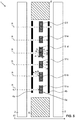
- Each data carrier 1 comprises a cover layer 2 and a base layer 3, wherein two processing layers 4a, 4b and one protection structure 5a (see figures 1a to 5 and figure 8 to 9 ) or four processing layers 4a, 4b, 4c, 4d and three protecting structures 5a, 5b, 5c (see figures 6a to 7 ) are arranged between the cover layer 2 and the base layer 3, respectively.
- the different embodiments shown here mainly differ in the number of processing layers and protecting structures, their composition, as well as in the processing of the processing layers. This is now explained in greater detail with respect to the individual figures.
- the data carrier 1 comprises, in this sequence along a first direction d1, a cover layer 2, a first processing layer 4a, a protection structure 5a, a second processing layer 4b, and a base layer 3.
- the cover layer 2 and the base layer 3 are provided made from plastics, here from polycarbonate (PC) or polyethylene terephthalate (PET). That is, both layers 2, 3 are essentially transparent or include printed elements. However, it is likewise conceivable to provide the base layer 3 in white or colored, for example as opaque layer.
- the processing layers 4a, 4b are metallic layers and the protection structure 5a in this example corresponds to an ink that is applied between the processing layers 4a, 4b along an extension direction E.
- the ink 5a is applied along an entire length of the processing layers 4a, 4b. That is, the processing layers 4a, 4b are completely separated from each other by the protection structure 5a.
- two opaque areas 6 are provided sideways to the processing layers 4a, 4b and the protection structure 5a and, with respect to the extension direction E, before and after the processing layers 4a, 4b and the protection structure 5a. Said opaque areas 6 serve the purpose of optically separating the front and back side of the document or containing electronical parts and devices.
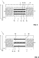
- FIG 1b the irradiation of electromagnetic radiation R along the first direction d1 as well as the irradiation of electromagnetic radiation R along a second direction d2 running opposite to the first direction d1 is shown.
- the electromagnetic radiation R irradiated along the first direction d1 ablates the first processing layer 4a
- the electromagnetic radiation R irradiated along the second direction d2 ablates the second processing layer 4b.
- the protection structure 5a prevents the electromagnetic radiation R from impinging on the second processing layer 4b and in the latter case the protection structure 5a prevents the electromagnetic radiation R from impinging on the first processing layer 4a, respectively.
- the protection structure 5a acts as a barrier or blockage for the respectively underlying processing layer 4a, 4b with regard to an irradiation from both sides of the data carrier 1.
- the blocking of the electromagnetic radiation R is based on absorption of this radiation by the components constituting the protection structure 5a, i.e. the ink.
- Said ink 5a could correspond to the inks spectraCARD IRB from Printcolor or MSD4800 and MSC3600 from H. W. Sands, which absorb in the infrared region of the electromagnetic spectrum.
- the MSC3600 ink is based on an absorbing dye. The ink absorbs almost totally in the range of 800 nm to 1050 nm.
- the irradiated electromagnetic radiation preferably corresponds to monochromatic radiation, particularly preferably to laser radiation, wherein the irradiation of laser radiation on the processing layers 4a, 4b results in an at least partial ablation, and here in a complete ablation of the processing layers 4a, 4b in the region of incident laser radiation.
- monochromatic radiation particularly preferably to laser radiation
- the irradiation of laser radiation on the processing layers 4a, 4b results in an at least partial ablation, and here in a complete ablation of the processing layers 4a, 4b in the region of incident laser radiation.
- the modified regions 41a, 41b together with the unmodified regions 42a, 42b represent a security feature such as personalized data or optical filters.
- Conceivable personalized data are graphical data, e.g. an image or a logo, or alphanumerical data, such as a name or a date of birth of the owner of the data carrier or machine-readable data, such as a barcode, respectively.
- An optical filter could be a Moiré-pattern, wherein a first part of the pattern is provided by means of the modified and unmodified regions 41a, 42a on the first processing layer 4a and a second part of the pattern is provided by means of the modified and unmodified regions 41b, 42b on the second processing layer 4b. Due to the fact that the protection structure 5a prevents an unintentional ablation of underlying processing layers, a precise production of a personalized or security-feature-bearing data carrier is enabled.
- FIGS 2 to 4 different embodiments of a data carrier 1 comprising two processing layers 4a, 4b and one protection structure 5a are shown.
- figure 2 disclose a data carrier 1 which further comprises an opaque area 6 that is arranged with respect to the first direction d1 between the second processing layer 4b and the base layer 3.
- the first and second processing layers 4a, 4b comprise some congruent recesses 43a, 43b that were formed by ablation and through which the opaque layer 6 is unravelled.
- These recesses 43a, 43b can be obtained by irradiating electromagnetic radiation constituting a spectrum of one or more wavelengths that can pass through the protection structure 5a.
- the first processing layer 4a comprises some recesses 44a that are only present on said first processing layer 4a but which are not on the second processing layer 4b.
- These recesses 44a can be obtained by irradiating electromagnetic radiation constituting a spectrum of one or more wavelengths that cannot pass through the protection structure 5a, e.g. because it is absorbed by the protection structure 5a.
- the electromagnetic radiation is only irradiated along the first direction d1, that is, along a direction extending from the cover layer 2 towards the base layer 3.
- a data carrier 1 which essentially corresponds to the data carrier 1 according to figure 1 , with the exception that a lens filter arrangement 7 is arranged on the cover layer 2.
- Said lens filter arrangement 7 serves the purpose of focussing incoming light onto particular regions of the security features. Hence, those parts of the security features where the incoming light has not been focussed to will not be illuminated.
- This partial or selective illumination of the security feature confers the security feature a changing appearance, wherein the appearance changes in dependence of the viewing angle.
- the filter arrangement can be produced on the data carrier during lamination of the data carrier. In doing so, the filter arrangement can be moulded from an embossing template onto the plastics constituting the cover layer 2 of the data carrier 1.
- the data carrier 1 shown in figure 4 essentially corresponds to the data carrier according to figure 1 , with the exception that a filter structure 8 is printed on the cover layer 2.
- Said printed filter structure 8 serves the same purpose as the filter arrangement 7 according to figure 3 .
- the filtering effect is realized by covering particular regions of the security feature and thus illuminating only a part of it.
- the printed filter structure 8 can be printed onto the cover layer 2 prior to the lamination of the data carrier 1. To this end offset or screen printing are typically used.
- a data carrier 1 comprising several kinds of protection structures 5a is depicted.
- said data carrier 1 comprises a transparent cover layer 2 and a transparent base layer 3 as well as two opaque areas 6 as it is the case with the data carrier 1 according to figure 1 .
- the protection structure 5a is provided in a fictitious and schematic manner for explanatory purposes.
- the different kinds of protection structures are indicated by the segments 51a-51f, which segments are arranged between the first processing layer 4a and the second processing layer 4b and which segments have different properties.
- a first segment 51a corresponds to a protection structure 5a that comprises a material configured to fully reflect a particular wavelength.
- the second segment 51b corresponds to a protection structure 5a which is also configured to reflect electromagnetic radiation R of a particular wavelength.
- the second segment 51b reflects the incident radiation R at various defined angles.
- both segments 51, 51b comprise a periodical structure provided on their surfaces, wherein said periodical structures are configured to fully reflect incident electromagnetic radiation R (first segment 51a) or to deflect incident electromagnetic radiation R (second segment 51b) of a particular wavelength.
- first segment 51a incident electromagnetic radiation
- second segment 51b deflect incident electromagnetic radiation
- the third segment 51c corresponds to a protection structure 5a which is configured to transmit impinging electromagnetic radiation R of a particular wavelength at various angles. Hence, if electromagnetic radiation R of said particular wavelength is irradiated, it will first ablate the first processing layer 4a and then impinge on the protection structure 51c, where it is deflected by the protection structure 51c while it passes through said protection structure 51c. This deflection is caused by the intrinsic properties of the protection structure 51c.
- said protection structure 51c can be understood as having a diffractive grid structure.
- the transmitted radiation is deflected towards the second processing layer 4b.
- the power of the deflected transmitted radiation is significantly smaller than the power of the incident radiation, the deflected radiation will not ablate the second processing layer 4b in case that it is deflected onto it.
- the fourth segment 51d corresponds to a protection structure 5a which comprises nanoparticles configured to diffusely scatter impinging electromagnetic radiation R of a particular wavelength.
- electromagnetic radiation R of said particular wavelength if electromagnetic radiation R of said particular wavelength is irradiated, it will first ablate the first processing layer 4a and then impinge on the fourth segment 51d, where it is scattered on the surfaces of the nanoparticles while it passes through said fourth segment 51d. In the present situation the radiation is scattered in all directions. However, since the power of the scattered radiation is significantly smaller than the power of the incident radiation, the scattered radiation will not ablate the first or second processing layers 4a, 4b in case that it is deflected onto them.
- the fifth and sixth segments 51e, 51f correspond to a protection structure 5a the incident electromagnetic radiation R is not sensitive to.
- these segments 51e, 51f could correspond to an ink that absorbs at a particular wavelength, wherein the incident radiation R has a wavelength being different from said particular wavelength. Therefore, the incident radiation R can pass through these segments 51e, 51f without being deflected or scattered.
- the power of the incident radiation R is not strong enough to ablate the second processing layer 4b after having ablated the first processing layer 4a and having passed the fifth segment 51e
- the power of the incident radiation R irradiated in the region of the sixth segment 51f is indeed strong enough to ablate the first processing layer 4a as well as the second processing layer 4b after having passed the sixth segment 51f.
- the data carriers 1 according to figures 6a to 7 comprise four processing layers 4a, 4b, 4c, 4d and three protection structures 5a, 5b, 5c.
- FIG. 6a the personalization of the data carrier 1 is depicted.
- a personalization of the first and fourth processing layers 4a, 4d is achieved in a first step by irradiating electromagnetic radiation R along the first direction d1 in order to selectively ablate the first processing layer 4a and by irradiating electromagnetic radiation R along the second direction d2 in order to selectively ablate the fourth processing layer 4d as shown in figure 6b .
- the first protection structure 5a arranged between the first and the second processing layers 4a, 4b and the third protection structure 5c arranged between the third and the fourth processing layers 4c, 4d block these irradiated radiations R, such that modified regions 41 a, 41d are created only in the first and fourth processing layers 4a, 4d.
- the wavelength of these irradiations R and thus also the wavelength-sensitivity of the first protection structure 5a and the third protection structure 5c are the same.
- radiation R having a wavelength being different from the wavelength of the radiation R irradiated in the first step is irradiated onto the data carrier 1 along the first direction d1 and along the second direction d2.
- This radiation R is irradiated at positions where the first and fourth processing layers 4a, 4d were already ablated in the first step.
- this radiation R is of a wavelength that can pass through the first protection structure 5a and the third protection structure 5c, such that the second processing layer 4b lying with respect to the first direction d1 beneath the first processing layer 4a and the third processing layer 4c lying with respect to the second direction d2 beneath the fourth processing layer 4d are selectively ablated.
- congruent recesses 43a, 43b in the first and second processing layers 4a, 4b and congruent recesses 43c, 43d in the third and fourth processing layers 4c, 4d are generated.
- the second protection structure 5b being arranged between the second and third processing layers 4b, 4c is configured to block said radiation R, the radiation R propagating along the first direction d1 is prevented from impinging on the third processing layer 4c and the radiation R propagating along the second direction d2 is prevented from impinging on the second processing layer 4b, respectively.
- the data carrier 1 depicted in figure 7 differs from the data carrier according 1 to figures 6a to 6c in that it comprises two opaque areas, wherein a first opaque area 6 extends at least partially between the second processing layer 4b and the third processing layer 4c along the extension direction E and a second opaque area extends at least partially between the third processing layer 4c and the fourth processing layer 4d.
- a congruent ablation of the second and the third processing layers 4b, 4c unravels the first opaque area 6
- a congruent ablation of the first, second and third processing layers 4a, 4b, 4c unravels the second opaque area 6.
- higher complexity or diversity can be added to the data carrier 1.
- a data carrier 1 which in each case comprise spacing layers 9a-9d.
- these data carriers 1 comprise in each case a cover layer 2, a base layer 3, two processing layers 4a, 4b and a protection structure 5a as described previously.
- a transparent spacing layer 9a-9d is arranged on both sides of the processing layers 4a, 4b ( figure 8 ) or on both sides of the protection structure 5a ( figure 9 ).
- the spacing layers 9a-9d serve the purpose of increasing the distance between the processing layers to improve or even enable an optical effect e.g. while tilting the document.
- a second reason can be from a production point of view. It can be the case that the processing layer will be provided on a spacing layer and not separately.
Abstract
A data carrier (1) comprises in this sequence along a first direction (d1) a cover layer (2), at least a first processing layer (4a) and a second processing layer (4b), and a base layer (3). The data carrier (1) further comprises at least one protection structure (5a) which is arranged between the first and second processing layers (4a, 4b). The protection structure (5a) is configured such that, upon irradiation of electromagnetic radiation (R) constituting a first spectrum along the first direction (d1), the protection structure (5a) essentially entirely prevents said electromagnetic radiation (R) from impinging on the second processing layer (4b). A method of producing a data carrier (1) comprises the steps of providing a cover layer (2), at least a first processing layer (4a) and a second processing layer (4b), a base layer (3) and at least one protection structure (5a). The protection structure (5a) is configured such that, upon irradiation of electromagnetic radiation (R) constituting a first spectrum along the first direction (d1), the protection structure (5a) essentially entirely prevents said electromagnetic radiation (R) from impinging on the second processing layer (4b).
Description
- The present invention relates to a data carrier according to the preamble of
claim 1, a security document comprising such a data carrier and the use of such a data carrier for producing a security document according to claims 11 and 12, respectively. It furthermore relates to a method of producing a data carrier according to claim 13. - A wide variety of measures in order to protect data carriers such as identity cards, passports, bank cards, etc., from forgers are known in the art. As such, the provision of security elements such as data which is assigned to an individual person owning the data carrier is common. These may include personalized data such as a name, a date of birth or a photo of the owner. When a data carrier is stolen a forger usually tries to modify or replace the personalized data on the stolen card. It is therefore an aim to prevent or at least complicate the modification or replacement of these data.
- One way of preventing unauthorized copying, alterations and forgeries on a data carriers lies in the provision of a clear or see-though portion in the body of a data carrier as is disclosed in
WO 2012/097463 . Said see-through portion comprises two or more metallic layers which are provided with a security feature such as a personalization by means of a laser ablation process. However, during the manufacturing of the data carrier while working with the laser on the upper metallic layer the underlying metallic layer is unintentionally slightly ablated, too. This is caused by the fact that part of the induced laser energy penetrates the upper metallic layer and impinges on the underlying metallic layer, whereby an at least partial ablation of the underlying metallic layer is caused. An adjustment of the laser power does not prevent an ablation of the underlying metallic layer. This unintentional damage of the underlying metallic layer decreases the contrast and functionality of the security feature. - It is an object of the present invention to provide a data carrier having a higher level of security. In particular, it is an object to provide a data carrier comprising contrasty information.
- This object is achieved with a data carrier according to
claim 1. In particular, a data carrier is provided which comprises in this sequence along a first direction: a cover layer, at least a first processing layer and a second processing layer, and a base layer. The first and second processing layers are configured to be processed by means of electromagnetic radiation. The data carrier further comprises at least one protection structure which is arranged between the first and second processing layers. The protection structure is configured such that, upon irradiation of electromagnetic radiation constituting a first spectrum along the first direction, the protection structure essentially entirely prevents said electromagnetic radiation from impinging on the second processing layer. - That is to say, the data carrier can be processed by irradiating electromagnetic radiation constituting a spectrum composed of one or more particular wavelengths, wherein the protection structure allows an impingement of said radiation only on the first, i.e. upper processing layer but prevents an impingement on the second, i.e. underlying processing layer. The protection structure can thus be seen as a blockage or barrier that eliminates electromagnetic radiation which is used to process the first processing layer and which passes the first processing layer towards the underlying second processing layer. In this way, the contrast of information introduced into the data carrier by means of the electromagnetic irradiation is enhanced and, as a result, a data carrier having an increased level of security is obtained.
- An essentially entire prevention in the context of the present invention means that typically more than 80%, preferably more than 90% of the impinging electromagnetic radiation is blocked by the processing structure.
- The electromagnetic radiation preferably corresponds to monochromatic radiation, particularly preferably to laser radiation, wherein the irradiation of laser radiation on the first processing layer results in an at least partial ablation of the first processing layer. In this way, the first processing layer is modified, wherein the modified region, potentially together with unmodified regions on the first processing layer and the unprocessed second processing layer, can represent a security feature such as personalized data. Conceivable personalized data are graphical data, e.g. an image or a logo, or alphanumerical data, such as a name or a date of birth of the owner of the data carrier or machine-readable data, such as a barcode, respectively.
- The protection structure can be configured such that, upon irradiation of the electromagnetic radiation constituting the first spectrum along a second direction running opposite to the first direction, the protection structure essentially entirely prevents said electromagnetic radiation from impinging on the first processing layer.
- In other words, the protection structure acts as a barrier or blockage for the respectively underlying processing layer with regard to an irradiation of the wavelength(s) constituting the first spectrum from both sides of the data carrier, i.e. against irradiation from a front side of the data carrier, wherein the irradiation propagates along the first direction extending from the cover layer towards the base layer, as well as against irradiation from a back side of the data carrier, wherein the irradiation propagates along the second direction extending from the base layer towards the cover layer. In this case the first processing layer is processed from the front side and the second processing layer is processed from the back side of the data carrier, wherein the processing of one of the processing layers does not affect the other processing layer. Hence, a precise production of a personalized or security-feature-bearing data carrier with the information provided on the at least two processing layers is enabled. The present invention is thus also very suitable for the provision of security features based on filters, such as Moire-patterns.
- The protection structure is preferably configured such that, upon irradiation of electromagnetic radiation constituting a second spectrum being different from the first spectrum along the first direction, the protection structure allows said electromagnetic radiation to impinge on the first processing layer and on the second processing layer. In addition or as an alternative the protection structure can be configured such, that upon irradiation of electromagnetic radiation constituting the second spectrum along the second direction, the protection structure allows said electromagnetic radiation to impinge on the second processing layer and on the first processing layer.
- As will be explained in greater detail below, the protection structure is preferably wavelength-specific. That is to say, the protection structure can be configured such that it allows the transmission of electromagnetic radiation of one or more particular wavelengths but at the same time prevents the transmission of electromagnetic radiation of other one or more wavelengths. For example, it is conceivable to provide a protection structure that is a barrier or blockage for electromagnetic radiation having a wavelength of λ1 = 355 nm but which enables the propagation of electromagnetic radiation having a wavelength of λ2 = 380 nm. If in a first step radiation λ1 = 355 nm is irradiated from the front side (back side) of the data carrier along the first direction (second direction), said radiation will at least partially ablate only the first processing layer (second processing layer) because a further propagation towards the second processing layer (first processing layer) is prevented by the protection structure. If then in a second step radiation λ2 = 380 nm is irradiated from the front side (back side) of the data carrier along the first direction (second direction) at positions where an ablation of the first processing layer (second processing layer) has already occurred during the first step, said radiation will propagate through the protection structure and will at least partially ablate also the second processing layer (first processing layer). In this way a data carrier is generated wherein data is selectively generated and visible in the first processing layer and the second processing.
- The protection structure can be configured to absorb impinging electromagnetic radiation constituting the first spectrum. Such a protection structure has the function of an optical filter and allows electromagnetic radiation of particular wavelengths to pass and at the same time prevents the propagation of electromagnetic radiation having other particular wavelengths.
- The protection structure can comprise one or more additives and/or one or more pigments and/or one or more dyes and/or one or more inks that are configured to absorb impinging electromagnetic radiation constituting the first spectrum, the protection structure being preferably configured to absorb in the ultraviolet region and/or in the infrared region.
- Hence, it is preferred to provide a protection structure which is essentially transparent in visible light. To this end a variety of additives and inks can be used and which are well known to the person skilled in the art. An example of an additive which absorbs electromagnetic radiation in the ultraviolet region is based on a 2-hydroxyphenyl-s-triazine derivative such as the commercially available Tinuvin® 1600 from BASF. Examples of inks which absorb in the infrared region are the commercially available spectraCARD IRB from Printcolor or MSD4800 or MSC3600 from H. W. Sands.
- If the protection structure is provided by means of additives it is preferred to apply them in the form of a matrix comprising them. For example, the additives can be dispersed into a polymer matrix by using standard extrusion equipment. A protection structure in the form of an ink can be applied directly onto the base layer or the cover layer, for example.
- The protection structure can be configured to reflect impinging electromagnetic radiation constituting the first spectrum, the protection structure preferably being configured to fully reflect or diffusely reflect impinging electromagnetic radiation constituting the first spectrum, or the protection structure can be configured to diffusely transmit impinging electromagnetic radiation constituting the first spectrum. A full reflection occurs when the angle of light incident on the protection structure equals the angle of the light reflected from the protection structure. A diffuse reflection, also known as scattered reflection, refers to the scattering of incident light at many angles. In this case the protection structure can be seen as a diffraction grating or an optical grating. A scattered transmission means that the power of the impinging electromagnetic radiation is reduced by the protection structure such, that a processing of the processing layer lying beneath the protection structure by means of the transmitted electromagnetic radiation is prevented.
- The protection structure can comprise periodical structures that are configured to diffract impinging electromagnetic radiation constituting the first spectrum, or the protection structure can comprise nanoparticles, such that impinging electromagnetic radiation constituting the first spectrum is scattered on a surface of the nanoparticles. A protection structure in the form of nanoparticles can be provided by means of nanoparticles embedded in a matrix, preferably in a plastic matrix. Conceivable nanoparticles are silicon dioxide (SiO2) and titanium dioxide (TiO2) nanoparticles, for example.
- Hence, in view of the above it can be said that the blockage or barrier provided by means of the protection structure can be based on the reflection, the transmission or the absorption of the electromagnetic radiation being irradiated in order to process the processing layers, wherein said reflection, transmission or absorption depends on the particular wavelength of the irradiated electromagnetic radiation and the intrinsic properties of the protection structure. To this end, the size and the composition of the nanoparticles can be used to effectuate a diffraction of electromagnetic radiation of particular wavelength(s). Likewise, a reflection, transmission or absorption occurring for electromagnetic radiation of particular wavelength(s) can be set based on the shape of the periodical structures provided on the protection structure or the chemical composition or the thickness of the protection structure.
- The protection structure can be provided in the form of one or more layers, wherein said one or more layers extends at least partially between the first and second processing layers along an extension direction, the protection structure preferably being provided in the form of an optical multilayer structure, such that impinging electromagnetic radiation is blocked by interference phenomena.
- Hence, it is possible to provide a protection structure in the form of a single layer that fully extends between the first and second processing layers and thereby completely separates the first and second processing layers from one another. However, the provision of two or more layers constituting the protection structure is likewise conceivable, wherein said two or more layers can be arranged adjacent to one another with respect to the extension direction. In this case it is preferred that the two or more layers differ in their intrinsic properties such that they act as a barrier or blockage for different wavelengths. Moreover, it is also conceivable to provide the protection structure in the form of an optical multilayer structure, i.e. as several thin multilayer structures, wherein the thin multi-layer structures effectuate a thin-film interference of the impinging electromagnetic radiation. That is, depending on the wavelength of the irradiated electromagnetic radiation and the thickness and the composition of the thin multilayers of the protection structure, the waves composing the electromagnetic radiation are reflected by the upper and lower boundaries of the protection structure and interfere with one another such that they eliminate each other.
- The first and/or second processing layers preferably comprise one or more metals or metal-compounds, and/or the cover layer and/or the base layer are preferably transparent and preferably made of plastics, particularly preferably made from a polycarbonate or from a polyethylene terephthalate.
- Metals, metal-compounds or pigments that are ablated or bleached upon irradiation with electromagnetic radiation are conceivable. However, if a security feature such as a colored personalization is desired, a colored metal, metal-compound pigment should be used. For example, conceivable metals can be selected from Al, Cu, Au, Ag, Ti or combinations thereof and conceivable metal-compounds can be selected from TiN, TiCN, CrN, ZrN, TiZrN, ZrCN, TiC, TiCrN, AITiN, TiAIN, diamond like carbon or combinations thereof. Conceivable pigments or colorants are pigments or colorants that are commonly used in the field of the invention, such as the pigments disclosed in
EP0327508 ,WO9635585 WO0136208 - The data carrier can comprise three or more processing layers and two or more protection structures, wherein the processing layers and the protection structures are preferably arranged alternating along the first direction. In this case it is preferred that the protection structures differ in their wavelength-selectivity. For example, the data carrier can comprise three processing layers, wherein the first protection structure is arranged between the first and the second processing layer and a second protection structure is arranged between the second and the third processing layer. It is then preferred that the first protection structure is selectively blocking the first wavelength and that the second protection structure is selectively blocking a second wavelength being different from the first wavelength. In this way the first processing layer can be processed with electromagnetic radiation constituting the first spectrum while the underlying second and third processing layers are protected by the first protection structure and the second processing layer can be processed with electromagnetic radiation constituting the second spectrum while the underlying third processing layer is protected, for example.
- In another aspect a security document comprising a data carrier as described above is provided, the security document preferably being an identity card, a passport, a credit card, a bank note or the like.
- At this point it should be understood that the data carrier per se can correspond to a security document. This is the case if the data carrier is provided in the form of an identity card, for example. However, it is likewise conceivable to introduce or incorporate the data carrier into a security document. In the case of a passport for example the data carrier could correspond to a page of the passport, wherein said page is made of plastics, i.e. the cover layer and the base layer, within which the processing layers and the one or more protection structures are arranged. A colored picture of the passport owner can then be provided by means of particularly modified processing layers, for example. However, other personalized data such as an image or a logo, or alphanumerical data, such as a name or a date of birth of the owner or machine-readable data, such as a barcode, or optical filters (e.g. a Moire pattern, see above) can be provided with high contrasts and precision, too. An incorporation of the data carrier into a security document can be achieved by simply laminating the data carrier into a security document.
- In another aspect, a data carrier as described above is used for producing a security document. For example, a security document can be produced by first laminating the "raw", i.e. unpersonalized data carrier into a security document such as a passport or the like and by then processing the processing layers with electromagnetic radiation in order to personalize it. However, it is also conceivable to produce a security document by first processing the processing layers with electromagnetic radiation and by then laminating the thus personalized data carrier into a security document such as a passport or the like.
- In another aspect a method of producing a data carrier, preferably a data carrier as described above, is provided, the method comprising the steps of:
- Providing, in this sequence along a first direction, a cover layer, at least a first processing layer and a second processing layer and a base layer, the first and second processing layers being configured to be processed by means of electromagnetic radiation; and
- Providing at least one protection structure between the first and second processing layers, the protection structure being configured such that, upon irradiation of electromagnetic radiation constituting a first spectrum along the first direction, the protection structure essentially entirely prevents said electromagnetic radiation from impinging on the second processing layer.
- As has already been described above, the protection structure protects underlying processing layers by being a barrier or blockage for electromagnetic radiation constituting a spectrum comprised of one or more particular wavelengths. As a result, the method allows the production of data carriers with high contrast and thus increased security.
- Electromagnetic radiation constituting the first spectrum can be irradiated along the first direction in order to at least partially ablate the first processing layer, and/or electromagnetic radiation constituting the first spectrum can be irradiated along a second direction running opposite to the first direction in order to at least partially ablate the second processing layer, wherein the protection structure essentially entirely prevents said electromagnetic radiation from impinging on the first processing layer.
- Electromagnetic radiation constituting a second spectrum being different from the first spectrum can be irradiated along the first direction in order to at least partially ablate the second processing layer, and/or the electromagnetic radiation constituting the second spectrum can be irradiated along the second direction in order to at least partially ablate the first processing layer.
- That is, and as has also been pointed out, the protection structure acts as a barrier or blockage for the respectively underlying processing layer with regard to an irradiation of the particular wavelength(s) it is sensitive to from both sides of the data carrier.
- If three or more processing layers are used it is preferred to use two or more protection structures that are in each case arranged between successive processing layers. These two or more protection structures are then preferably selective for one particular wavelength only, wherein the two or more particular wavelengths differ from one another.
- In order to ablate or bleach the processing layers a wide range of laser wavelengths are conceivable. Typically, a fiber laser or crystal based solid state laser emitting at a wavelength of 1064 nm or 355 nm is selected.
- With respect to geometrical dimensions of the individual layers of the data carrier it can be said that a conceivable thickness of the processing layer lies in the range of about 10 nanometer to 50 micrometer. In particular, a conceivable thickness of a metallic or metal-compound comprising processing layer is about 20 nanometer, and a processing layer comprising pigments typically has a thickness of about 4 micrometer. The protection structure preferably has a thickness in the range of about 1 to 500 micrometer. In particular, if a protection structure being configured as a diffraction grating or an optical grating is used, a preferred thickness is 2 micrometer. In the case of a protection structure comprising a multilayer structure a typical thickness corresponds to 40 micrometer. A protection structure comprising absorbing additives or a protection structure comprising nanoparticles dispersed in a matrix typically has a thickness of about 100 micrometer.
- Preferred embodiments of the invention are described in the following with reference to the drawings, which are for the purpose of illustrating the present preferred embodiments of the invention and not for the purpose of limiting the same. In the drawings,
-
Fig. 1a shows a schematic representation of a data carrier according to a first embodiment in an unprocessed state; -
Fig. 1b shows a schematic representation of the data carrier according tofigure 1a during processing; -
Fig. 1c shows a schematic representation of the data carrier according tofigure 1a after processing; -
Fig. 2 shows a schematic representation of a data carrier according to a second embodiment; -
Fig. 3 shows a schematic representation of a data carrier according to a third embodiment; -
Fig. 4 shows a schematic representation of a data carrier according to a fourth embodiment; -
Fig. 5 shows a schematic representation of different processing possibilities of a fictitious data carrier according to a fifth embodiment; -
Fig. 6a shows a schematic representation of a data carrier according to a sixth embodiment in an unprocessed state; -
Fig. 6b shows a schematic representation of the data carrier according tofigure 6a during a first processing step; -
Fig. 6c shows a schematic representation of the data carrier according tofigure 6b during a second processing step; -
Fig. 6d shows a schematic representation of the data carrier according tofigure 6a after processing; -
Fig. 7 shows a schematic representation of a data carrier according to a seventh embodiment; -
Fig. 8 shows a schematic representation of a data carrier according to an eight embodiment; -
Fig. 9 shows a schematic representation of a data carrier according to a ninth embodiment. - Several embodiments of a
data carrier 1 according to the invention are depicted infigures 1 to 9 . Eachdata carrier 1 comprises acover layer 2 and abase layer 3, wherein twoprocessing layers protection structure 5a (seefigures 1a to 5 andfigure 8 to 9 ) or fourprocessing layers structures figures 6a to 7 ) are arranged between thecover layer 2 and thebase layer 3, respectively. The different embodiments shown here mainly differ in the number of processing layers and protecting structures, their composition, as well as in the processing of the processing layers. This is now explained in greater detail with respect to the individual figures. - The
data carrier 1 according tofigures 1a to 1c comprises, in this sequence along a first direction d1, acover layer 2, afirst processing layer 4a, aprotection structure 5a, asecond processing layer 4b, and abase layer 3. Thecover layer 2 and thebase layer 3 are provided made from plastics, here from polycarbonate (PC) or polyethylene terephthalate (PET). That is, bothlayers base layer 3 in white or colored, for example as opaque layer. The processing layers 4a, 4b are metallic layers and theprotection structure 5a in this example corresponds to an ink that is applied between theprocessing layers ink 5a is applied along an entire length of theprocessing layers processing layers protection structure 5a. In addition, twoopaque areas 6 are provided sideways to theprocessing layers protection structure 5a and, with respect to the extension direction E, before and after theprocessing layers opaque areas 6 serve the purpose of optically separating the front and back side of the document or containing electronical parts and devices. - In
figure 1b the irradiation of electromagnetic radiation R along the first direction d1 as well as the irradiation of electromagnetic radiation R along a second direction d2 running opposite to the first direction d1 is shown. As indicated in the figure, the electromagnetic radiation R irradiated along the first direction d1 ablates thefirst processing layer 4a and the electromagnetic radiation R irradiated along the second direction d2 ablates thesecond processing layer 4b. In the former case theprotection structure 5a prevents the electromagnetic radiation R from impinging on thesecond processing layer 4b and in the latter case theprotection structure 5a prevents the electromagnetic radiation R from impinging on thefirst processing layer 4a, respectively. Hence, theprotection structure 5a acts as a barrier or blockage for the respectivelyunderlying processing layer data carrier 1. In the present case, the blocking of the electromagnetic radiation R is based on absorption of this radiation by the components constituting theprotection structure 5a, i.e. the ink.Said ink 5a could correspond to the inks spectraCARD IRB from Printcolor or MSD4800 and MSC3600 from H. W. Sands, which absorb in the infrared region of the electromagnetic spectrum. The MSC3600 ink is based on an absorbing dye. The ink absorbs almost totally in the range of 800 nm to 1050 nm. - It should be noted that it is likewise conceivable to use inks that absorb in the ultraviolet region. Moreover, an absorbance of incident radiation could also be achieved by means of additives absorbing ultraviolet and/or infrared radiation. Regarding protection structures that block incident radiation based on other phenomena than absorbance will be discussed with respect to the other figures further below.
- The irradiated electromagnetic radiation preferably corresponds to monochromatic radiation, particularly preferably to laser radiation, wherein the irradiation of laser radiation on the
processing layers processing layers regions unmodified regions second processing layers - The modified
regions unmodified regions unmodified regions first processing layer 4a and a second part of the pattern is provided by means of the modified andunmodified regions second processing layer 4b. Due to the fact that theprotection structure 5a prevents an unintentional ablation of underlying processing layers, a precise production of a personalized or security-feature-bearing data carrier is enabled. - In
figures 2 to 4 , different embodiments of adata carrier 1 comprising twoprocessing layers protection structure 5a are shown. In particular,figure 2 disclose adata carrier 1 which further comprises anopaque area 6 that is arranged with respect to the first direction d1 between thesecond processing layer 4b and thebase layer 3. As follows from this figure, the first andsecond processing layers congruent recesses opaque layer 6 is unravelled. Theserecesses protection structure 5a. Moreover, thefirst processing layer 4a comprises somerecesses 44a that are only present on saidfirst processing layer 4a but which are not on thesecond processing layer 4b. Theserecesses 44a can be obtained by irradiating electromagnetic radiation constituting a spectrum of one or more wavelengths that cannot pass through theprotection structure 5a, e.g. because it is absorbed by theprotection structure 5a. In this example the electromagnetic radiation is only irradiated along the first direction d1, that is, along a direction extending from thecover layer 2 towards thebase layer 3. - In
figure 3 adata carrier 1 is shown which essentially corresponds to thedata carrier 1 according tofigure 1 , with the exception that alens filter arrangement 7 is arranged on thecover layer 2. Saidlens filter arrangement 7 serves the purpose of focussing incoming light onto particular regions of the security features. Hence, those parts of the security features where the incoming light has not been focussed to will not be illuminated. This partial or selective illumination of the security feature confers the security feature a changing appearance, wherein the appearance changes in dependence of the viewing angle. The filter arrangement can be produced on the data carrier during lamination of the data carrier. In doing so, the filter arrangement can be moulded from an embossing template onto the plastics constituting thecover layer 2 of thedata carrier 1. - Also the
data carrier 1 shown infigure 4 essentially corresponds to the data carrier according tofigure 1 , with the exception that afilter structure 8 is printed on thecover layer 2. Said printedfilter structure 8 serves the same purpose as thefilter arrangement 7 according tofigure 3 . The filtering effect is realized by covering particular regions of the security feature and thus illuminating only a part of it. The printedfilter structure 8 can be printed onto thecover layer 2 prior to the lamination of thedata carrier 1. To this end offset or screen printing are typically used. - In
figure 5 adata carrier 1 comprising several kinds ofprotection structures 5a is depicted. In particular, saiddata carrier 1 comprises atransparent cover layer 2 and atransparent base layer 3 as well as twoopaque areas 6 as it is the case with thedata carrier 1 according tofigure 1 . However, here theprotection structure 5a is provided in a fictitious and schematic manner for explanatory purposes. The different kinds of protection structures are indicated by thesegments 51a-51f, which segments are arranged between thefirst processing layer 4a and thesecond processing layer 4b and which segments have different properties. Namely, afirst segment 51a corresponds to aprotection structure 5a that comprises a material configured to fully reflect a particular wavelength. Hence, if electromagnetic radiation R of said particular wavelength is irradiated, it ablates thefirst processing layer 4a and it is then fully reflected on thefirst segment 51a of theprotection structure 5a, whereby a further propagation towards thesecond processing layer 4b is prevented. Thesecond segment 51b corresponds to aprotection structure 5a which is also configured to reflect electromagnetic radiation R of a particular wavelength. In contrast to thefirst segment 51a however, wherein the incident radiation R of the particular wavelength is reflected under the angle of incidence, thesecond segment 51b reflects the incident radiation R at various defined angles. To this end bothsegments 51, 51b comprise a periodical structure provided on their surfaces, wherein said periodical structures are configured to fully reflect incident electromagnetic radiation R (first segment 51a) or to deflect incident electromagnetic radiation R (second segment 51b) of a particular wavelength. Hence, with regard to thesecond segment 51b, if electromagnetic radiation R of said particular wavelength is irradiated, it will ablate thefirst processing layer 4a in a first step and then impinge on the surface of thesecond segment 51b, where the incident radiation R is deflected by the periodic structure provided on the surface of thesecond segment 51b at various angles of deflection. In fact, the radiation is deflected in several directions leading away from thesecond processing layer 4b. In the present situation, the radiation is deflected towards thefirst processing layer 4a. Because the power of the deflected radiation is significantly smaller than the power of the incident radiation R, the deflected radiation will not ablate thefirst processing layer 4a in case that it is deflected onto it. Thethird segment 51c corresponds to aprotection structure 5a which is configured to transmit impinging electromagnetic radiation R of a particular wavelength at various angles. Hence, if electromagnetic radiation R of said particular wavelength is irradiated, it will first ablate thefirst processing layer 4a and then impinge on theprotection structure 51c, where it is deflected by theprotection structure 51c while it passes through saidprotection structure 51c. This deflection is caused by the intrinsic properties of theprotection structure 51c. In fact, saidprotection structure 51c can be understood as having a diffractive grid structure. In the present situation, the transmitted radiation is deflected towards thesecond processing layer 4b. However, since the power of the deflected transmitted radiation is significantly smaller than the power of the incident radiation, the deflected radiation will not ablate thesecond processing layer 4b in case that it is deflected onto it. Thefourth segment 51d corresponds to aprotection structure 5a which comprises nanoparticles configured to diffusely scatter impinging electromagnetic radiation R of a particular wavelength. Hence, if electromagnetic radiation R of said particular wavelength is irradiated, it will first ablate thefirst processing layer 4a and then impinge on thefourth segment 51d, where it is scattered on the surfaces of the nanoparticles while it passes through saidfourth segment 51d. In the present situation the radiation is scattered in all directions. However, since the power of the scattered radiation is significantly smaller than the power of the incident radiation, the scattered radiation will not ablate the first orsecond processing layers sixth segments protection structure 5a the incident electromagnetic radiation R is not sensitive to. For example, thesesegments segments fifth segment 51e the power of the incident radiation R is not strong enough to ablate thesecond processing layer 4b after having ablated thefirst processing layer 4a and having passed thefifth segment 51e, the power of the incident radiation R irradiated in the region of thesixth segment 51f is indeed strong enough to ablate thefirst processing layer 4a as well as thesecond processing layer 4b after having passed thesixth segment 51f. - As already mentioned, the
data carriers 1 according tofigures 6a to 7 comprise fourprocessing layers protection structures - With respect to
figures 6a to 6c the personalization of thedata carrier 1 is depicted. In particular, starting from theunprocessed data carrier 1 according tofigure 6a , a personalization of the first andfourth processing layers first processing layer 4a and by irradiating electromagnetic radiation R along the second direction d2 in order to selectively ablate thefourth processing layer 4d as shown infigure 6b . Thefirst protection structure 5a arranged between the first and thesecond processing layers third protection structure 5c arranged between the third and the fourth processing layers 4c, 4d block these irradiated radiations R, such that modifiedregions fourth processing layers first protection structure 5a and thethird protection structure 5c are the same. However, it is likewise conceivable to irradiate radiations that differ in their wavelengths. In this case protection structures being selective for the particular wavelengths would have to be used. In the second step as shown infigure 6c , radiation R having a wavelength being different from the wavelength of the radiation R irradiated in the first step is irradiated onto thedata carrier 1 along the first direction d1 and along the second direction d2. This radiation R is irradiated at positions where the first andfourth processing layers first protection structure 5a and thethird protection structure 5c, such that thesecond processing layer 4b lying with respect to the first direction d1 beneath thefirst processing layer 4a and thethird processing layer 4c lying with respect to the second direction d2 beneath thefourth processing layer 4d are selectively ablated. In this way,congruent recesses second processing layers congruent recesses second protection structure 5b being arranged between the second andthird processing layers third processing layer 4c and the radiation R propagating along the second direction d2 is prevented from impinging on thesecond processing layer 4b, respectively. Hence, by providingseveral processing layers 4a-4d andseveral protection structures unmodified regions 41a-41d, 42a-42d and corresponding at least partiallycongruent recesses 43a-43d as well asunique recesses 44a-44d are created, which enables the production of amultilayer data carrier 1 comprising complex security features at high precision. - The
data carrier 1 depicted infigure 7 differs from the data carrier according 1 tofigures 6a to 6c in that it comprises two opaque areas, wherein a firstopaque area 6 extends at least partially between thesecond processing layer 4b and thethird processing layer 4c along the extension direction E and a second opaque area extends at least partially between thethird processing layer 4c and thefourth processing layer 4d. In this case a congruent ablation of the second and thethird processing layers opaque area 6 and a congruent ablation of the first, second andthird processing layers opaque area 6. Depending on the appearance such as the color of the opaque areas, higher complexity or diversity can be added to thedata carrier 1. - In
figures 8 and 9 two different embodiments of adata carrier 1 are depicted, which in each case comprisespacing layers 9a-9d. In particular, thesedata carriers 1 comprise in each case acover layer 2, abase layer 3, twoprocessing layers protection structure 5a as described previously. In addition however, atransparent spacing layer 9a-9d is arranged on both sides of theprocessing layers figure 8 ) or on both sides of theprotection structure 5a (figure 9 ). The spacing layers 9a-9d serve the purpose of increasing the distance between the processing layers to improve or even enable an optical effect e.g. while tilting the document. A second reason can be from a production point of view. It can be the case that the processing layer will be provided on a spacing layer and not separately. -
- 1
- data carrier
- 2
- cover layer
- 3
- base layer
- 4a-4d
- processing layer
- 41a-41d
- modified region
- 42a-42d
- unmodified region
- 43a-43d
- recess
- 44a-44d
- recess
- 5a-5c
- protecting structure
- 51a-51f
- segment
- 6
- opaque area
- 7
- lens filter arrangement
- 8
- filter structure
- 9a-9d
- spacing layer
- R
- electromagnetic radiation
- d1
- first direction
- d2
- second direction
- E
- extension direction
Claims (15)
- A data carrier (1) comprising in this sequence along a first direction (d1):- a cover layer (2);- at least a first processing layer (4a) and a second processing layer (4b); and- a base layer (3),wherein the first and second processing layers (4a, 4b) are configured to be processed by means of electromagnetic radiation (R), characterized in thatthe data carrier (1) further comprises at least one protection structure (5a) which is arranged between the first and second processing layers (4a, 4b),wherein the protection structure (5a) is configured such that, upon irradiation of electromagnetic radiation (R) constituting a first spectrum along the first direction (d1), the protection structure (5a) essentially entirely prevents said electromagnetic radiation (R) from impinging on the second processing layer (4b).
- The data carrier (1) according to claim 1, wherein the protection structure (5a) is configured such that, upon irradiation of the electromagnetic radiation (R) constituting the first spectrum along a second direction (d2) running opposite to the first direction (d1), the protection structure (5a) essentially entirely prevents said electromagnetic radiation (R) from impinging on the first processing layer (4a).
- The data carrier (1) according to claim 1 or 2, wherein the protection structure (5a) is configured such that, upon irradiation of electromagnetic radiation (R) constituting a second spectrum being different from the first spectrum along the first direction (d1), the protection structure (5a) allows said electromagnetic radiation (R) to impinge on the first processing layer (4a) and on the second processing layer (4b), and/or
wherein the protection structure (5a) is configured such, that upon irradiation of electromagnetic radiation (R) constituting the second spectrum along the second direction (d2), the protection structure (5a) allows said electromagnetic radiation (R) to impinge on the second processing layer (4b) and on the first processing layer (4a). - The data carrier (1) according to any one of the preceding claims, wherein the protection structure (5a) is configured to absorb impinging electromagnetic radiation (R) constituting the first spectrum.
- The data carrier (1) according to any one of the preceding claims, wherein the protection structure (5a) comprises one or more additives and/or one or more pigments and/or one or more dyes and/or one or more inks that are configured to absorb impinging electromagnetic radiation (R) constituting the first spectrum, the protection structure (5a) preferably being configured to absorb in the ultraviolet region and/or in the infrared region.
- The data carrier (1) according to any one of the preceding claims, wherein the protection structure (5a) is configured to reflect impinging electromagnetic radiation (R) constituting the first spectrum, the protection structure (5a) preferably being configured to fully reflect or diffusely reflect impinging electromagnetic radiation (R) constituting the first spectrum, or
wherein the protection structure (5a) is configured to diffusely transmit impinging electromagnetic radiation (R) constituting the first spectrum. - The data carrier (1) according to any one of the preceding claims, wherein the protection structure (5a) comprises periodical structures that are configured to diffract impinging electromagnetic radiation (R) constituting the first spectrum; or
wherein the protection structure (5a) comprises nanoparticles, such that impinging electromagnetic radiation (R) constituting the first spectrum is scattered on a surface of the nanoparticles. - The data carrier (1) according to any one of the preceding claims, wherein the protection structure (5a) is provided in the form of one or more layers, wherein said one or more layers extend at least partially between the first and second processing layers (4a, 4b) along an extension direction (E), the protection structure (5a) preferably being provided in the form of an optical multilayer structure, such that impinging electromagnetic radiation (R) is blocked by interference phenomena.
- The data carrier (1) according to any one of the preceding claims, wherein the first and/or second processing layers (4a, 4b) comprise one or more metals or metal-compounds, and/or
wherein the cover layer (2) and/or the base layer (3) are transparent and preferably made of plastics, particularly preferably made from a polycarbonate or from a polyethylene terephthalate. - The data carrier (1) according to any one of the preceding claims, further comprising three or more processing layers (4c, 4d) and two or more protection structures (5b, 5c), wherein the processing layers (4a-4d) and the protection structures (5a-5c) are preferably arranged alternating along the first direction (d1).
- A security document comprising a data carrier (1) according to any one of the preceding claims, the security document preferably being an identity card, a passport, a credit card, a bank note or the like.
- Use of a data carrier (1) according to any one of claims 1 to 10 for producing a security document.
- A method of producing a data carrier (1), preferably a data carrier (1) according to any one of claims 1 to 10, the method comprising the steps of:- Providing, in this sequence along a first direction (d1), a cover layer (2), at least a first processing layer (4a) and a second processing layer (4b) and a base layer (3), the first and second processing layers (4a, 4b) being configured to be processed by means of electromagnetic radiation (R); and- Providing at least one protection structure (5a) between the first and second processing layers (4a, 4b), the protection structure (5a) being configured such that, upon irradiation of electromagnetic radiation (R) constituting a first spectrum along the first direction (d1), the protection structure (5a) essentially entirely prevents said electromagnetic radiation (R) from impinging on the second processing layer (4b).
- The method according to claim 13, wherein electromagnetic radiation (R) constituting the first spectrum is irradiated along the first direction (d1) in order to at least partially ablate the first processing layer (4a), and/or
wherein electromagnetic radiation (R) constituting the first spectrum is irradiated along a second direction (d2) running opposite to the first direction (d1) in order to at least partially ablate the second processing layer (4b), wherein the protection structure (5a) essentially entirely prevents said electromagnetic radiation (R) from impinging on the first processing layer (4a). - The method according to claim 14, wherein electromagnetic radiation (R) constituting a second spectrum being different from the first spectrum is irradiated along the first direction (d1) in order to at least partially ablate the second processing layer (4b), and/or
wherein the electromagnetic radiation (R) constituting the second spectrum is irradiated along the second direction (d2) in order to at least partially ablate the first processing layer (4a).
Priority Applications (2)
| Application Number | Priority Date | Filing Date | Title |
|---|---|---|---|
| EP19170398.2A EP3674098A1 (en) | 2018-12-28 | 2019-04-19 | Ablation blockers |
| PCT/EP2020/060343 WO2020212289A1 (en) | 2019-04-19 | 2020-04-10 | Ablation blockers |
Applications Claiming Priority (2)
| Application Number | Priority Date | Filing Date | Title |
|---|---|---|---|
| EP18248271 | 2018-12-28 | ||
| EP19170398.2A EP3674098A1 (en) | 2018-12-28 | 2019-04-19 | Ablation blockers |
Publications (1)
| Publication Number | Publication Date |
|---|---|
| EP3674098A1 true EP3674098A1 (en) | 2020-07-01 |
Family
ID=65010489
Family Applications (1)
| Application Number | Title | Priority Date | Filing Date |
|---|---|---|---|
| EP19170398.2A Withdrawn EP3674098A1 (en) | 2018-12-28 | 2019-04-19 | Ablation blockers |
Country Status (1)
| Country | Link |
|---|---|
| EP (1) | EP3674098A1 (en) |
Cited By (1)
| Publication number | Priority date | Publication date | Assignee | Title |
|---|---|---|---|---|
| EP4098455A1 (en) * | 2021-06-02 | 2022-12-07 | Thales DIS France SA | Ablative printed metallic layer |
Citations (8)
| Publication number | Priority date | Publication date | Assignee | Title |
|---|---|---|---|---|
| EP0327508A2 (en) | 1988-02-03 | 1989-08-09 | Ciba-Geigy Ag | Process for laser marking of pigmented systems |
| WO1996035585A1 (en) | 1995-05-10 | 1996-11-14 | Dsm N.V. | Method for the manufacture of a coloured mark |
| WO2001036208A2 (en) | 1999-11-18 | 2001-05-25 | Orga Kartensysteme Gmbh | Method for applying coloured information on an object |
| US20050161512A1 (en) * | 2001-12-24 | 2005-07-28 | Jones Robert L. | Optically variable personalized indicia for identification documents |
| EP1935663A1 (en) * | 2006-12-18 | 2008-06-25 | Setec Oy | Data carrier with see-through window and method for producing it |
| EP1983473A1 (en) * | 2003-11-12 | 2008-10-22 | Giesecke & Devrient GmbH | Data carrier with codes |
| WO2012097463A1 (en) | 2011-01-18 | 2012-07-26 | Trüb AG | Method for producing a multilayer data carrier and data carrier produced by said method |
| FR3050140A1 (en) * | 2016-04-15 | 2017-10-20 | Smart Packaging Solutions | SAFETY DOCUMENT WITH LASER PRINTING THROUGH OPAQUE INK |
-
2019
- 2019-04-19 EP EP19170398.2A patent/EP3674098A1/en not_active Withdrawn
Patent Citations (8)
| Publication number | Priority date | Publication date | Assignee | Title |
|---|---|---|---|---|
| EP0327508A2 (en) | 1988-02-03 | 1989-08-09 | Ciba-Geigy Ag | Process for laser marking of pigmented systems |
| WO1996035585A1 (en) | 1995-05-10 | 1996-11-14 | Dsm N.V. | Method for the manufacture of a coloured mark |
| WO2001036208A2 (en) | 1999-11-18 | 2001-05-25 | Orga Kartensysteme Gmbh | Method for applying coloured information on an object |
| US20050161512A1 (en) * | 2001-12-24 | 2005-07-28 | Jones Robert L. | Optically variable personalized indicia for identification documents |
| EP1983473A1 (en) * | 2003-11-12 | 2008-10-22 | Giesecke & Devrient GmbH | Data carrier with codes |
| EP1935663A1 (en) * | 2006-12-18 | 2008-06-25 | Setec Oy | Data carrier with see-through window and method for producing it |
| WO2012097463A1 (en) | 2011-01-18 | 2012-07-26 | Trüb AG | Method for producing a multilayer data carrier and data carrier produced by said method |
| FR3050140A1 (en) * | 2016-04-15 | 2017-10-20 | Smart Packaging Solutions | SAFETY DOCUMENT WITH LASER PRINTING THROUGH OPAQUE INK |
Cited By (2)
| Publication number | Priority date | Publication date | Assignee | Title |
|---|---|---|---|---|
| EP4098455A1 (en) * | 2021-06-02 | 2022-12-07 | Thales DIS France SA | Ablative printed metallic layer |
| WO2022253972A1 (en) * | 2021-06-02 | 2022-12-08 | Thales Dis France Sas | Ablative printed metallic layer |
Similar Documents
| Publication | Publication Date | Title |
|---|---|---|
| AU2016222386B2 (en) | Method for producing a multilayer data carrier and data carrier produced by said method | |
| RU2499674C1 (en) | Data carrier having window | |
| EP3697624B1 (en) | Security devices, security articles, security documents and methods for their manufacture | |
| AU2011325516B2 (en) | Security element and method for producing a security element | |
| US20070085337A1 (en) | Data carrier and method for manufacturing the same | |
| EP3697623B1 (en) | Security documents and methods of manufacture thereof | |
| US20090315316A1 (en) | Method of generating a laser mark in a security document, and security document of this kind | |
| US20160110638A1 (en) | Optically Variable Security Element | |
| US20100290039A1 (en) | Data Carrier Having Identifiers | |
| WO2010121293A1 (en) | Optically variable device and security document including same | |
| CA2578012C (en) | Security document with a volume hologram forming a partial motif | |
| EP3674098A1 (en) | Ablation blockers | |
| RU2586812C2 (en) | Protective device with variable optical properties for valuable documents | |
| JP7461496B2 (en) | Data carriers protected against subsequent laser marking | |
| EP3956148A1 (en) | Ablation blockers | |
| WO2020212289A1 (en) | Ablation blockers | |
| EP3674100A1 (en) | Multilayer ablation features | |
| EP3956149A1 (en) | Multilayer ablation features | |
| WO2020212288A1 (en) | Multilayer ablation features | |
| EP4098455A1 (en) | Ablative printed metallic layer | |
| GB2584552A (en) | Security devices, security articles, security documents and methods for their manufacture | |
| NZ707967B2 (en) | Method for producing a multilayer data carrier and data carrier produced by said method |
Legal Events
| Date | Code | Title | Description |
|---|---|---|---|
| PUAI | Public reference made under article 153(3) epc to a published international application that has entered the european phase |
Free format text: ORIGINAL CODE: 0009012 |
|
| STAA | Information on the status of an ep patent application or granted ep patent |
Free format text: STATUS: THE APPLICATION HAS BEEN PUBLISHED |
|
| AK | Designated contracting states |
Kind code of ref document: A1 Designated state(s): AL AT BE BG CH CY CZ DE DK EE ES FI FR GB GR HR HU IE IS IT LI LT LU LV MC MK MT NL NO PL PT RO RS SE SI SK SM TR |
|
| AX | Request for extension of the european patent |
Extension state: BA ME |
|
| STAA | Information on the status of an ep patent application or granted ep patent |
Free format text: STATUS: THE APPLICATION IS DEEMED TO BE WITHDRAWN |
|
| 18D | Application deemed to be withdrawn |
Effective date: 20210112 |