EP3648967B1 - Optical structures providing dichroic effects - Google Patents
Optical structures providing dichroic effects Download PDFInfo
- Publication number
- EP3648967B1 EP3648967B1 EP18863912.4A EP18863912A EP3648967B1 EP 3648967 B1 EP3648967 B1 EP 3648967B1 EP 18863912 A EP18863912 A EP 18863912A EP 3648967 B1 EP3648967 B1 EP 3648967B1
- Authority
- EP
- European Patent Office
- Prior art keywords
- equal
- optical structure
- color
- degrees
- layer
- Prior art date
- Legal status (The legal status is an assumption and is not a legal conclusion. Google has not performed a legal analysis and makes no representation as to the accuracy of the status listed.)
- Active
Links
- 230000003287 optical effect Effects 0.000 title claims description 412
- 230000000694 effects Effects 0.000 title description 16
- 229910052751 metal Inorganic materials 0.000 claims description 177
- 239000002184 metal Substances 0.000 claims description 177
- 230000005540 biological transmission Effects 0.000 claims description 103
- 239000000049 pigment Substances 0.000 claims description 72
- VYPSYNLAJGMNEJ-UHFFFAOYSA-N Silicium dioxide Chemical compound O=[Si]=O VYPSYNLAJGMNEJ-UHFFFAOYSA-N 0.000 claims description 55
- MCMNRKCIXSYSNV-UHFFFAOYSA-N ZrO2 Inorganic materials O=[Zr]=O MCMNRKCIXSYSNV-UHFFFAOYSA-N 0.000 claims description 37
- 230000003595 spectral effect Effects 0.000 claims description 33
- BQCADISMDOOEFD-UHFFFAOYSA-N Silver Chemical compound [Ag] BQCADISMDOOEFD-UHFFFAOYSA-N 0.000 claims description 29
- 229910052709 silver Inorganic materials 0.000 claims description 29
- 239000004332 silver Substances 0.000 claims description 29
- 238000002834 transmittance Methods 0.000 claims description 29
- 229920000642 polymer Polymers 0.000 claims description 28
- 239000003973 paint Substances 0.000 claims description 18
- 239000000377 silicon dioxide Substances 0.000 claims description 16
- CETPSERCERDGAM-UHFFFAOYSA-N ceric oxide Chemical compound O=[Ce]=O CETPSERCERDGAM-UHFFFAOYSA-N 0.000 claims description 9
- 229910000422 cerium(IV) oxide Inorganic materials 0.000 claims description 9
- 239000005083 Zinc sulfide Substances 0.000 claims description 7
- 229910052984 zinc sulfide Inorganic materials 0.000 claims description 7
- 229910052782 aluminium Inorganic materials 0.000 claims description 6
- XAGFODPZIPBFFR-UHFFFAOYSA-N aluminium Chemical compound [Al] XAGFODPZIPBFFR-UHFFFAOYSA-N 0.000 claims description 6
- PCHJSUWPFVWCPO-UHFFFAOYSA-N gold Chemical compound [Au] PCHJSUWPFVWCPO-UHFFFAOYSA-N 0.000 claims description 6
- 229910052737 gold Inorganic materials 0.000 claims description 6
- 239000010931 gold Substances 0.000 claims description 6
- XOLBLPGZBRYERU-UHFFFAOYSA-N tin dioxide Chemical compound O=[Sn]=O XOLBLPGZBRYERU-UHFFFAOYSA-N 0.000 claims description 6
- ZNOKGRXACCSDPY-UHFFFAOYSA-N tungsten trioxide Chemical compound O=[W](=O)=O ZNOKGRXACCSDPY-UHFFFAOYSA-N 0.000 claims description 6
- 229910001316 Ag alloy Inorganic materials 0.000 claims description 4
- 229910003437 indium oxide Inorganic materials 0.000 claims description 4
- PJXISJQVUVHSOJ-UHFFFAOYSA-N indium(iii) oxide Chemical compound [O-2].[O-2].[O-2].[In+3].[In+3] PJXISJQVUVHSOJ-UHFFFAOYSA-N 0.000 claims description 4
- AMGQUBHHOARCQH-UHFFFAOYSA-N indium;oxotin Chemical compound [In].[Sn]=O AMGQUBHHOARCQH-UHFFFAOYSA-N 0.000 claims description 4
- RUDFQVOCFDJEEF-UHFFFAOYSA-N oxygen(2-);yttrium(3+) Chemical compound [O-2].[O-2].[O-2].[Y+3].[Y+3] RUDFQVOCFDJEEF-UHFFFAOYSA-N 0.000 claims description 4
- GWEVSGVZZGPLCZ-UHFFFAOYSA-N Titan oxide Chemical compound O=[Ti]=O GWEVSGVZZGPLCZ-UHFFFAOYSA-N 0.000 claims description 3
- 229910001635 magnesium fluoride Inorganic materials 0.000 claims description 3
- BPUBBGLMJRNUCC-UHFFFAOYSA-N oxygen(2-);tantalum(5+) Chemical compound [O-2].[O-2].[O-2].[O-2].[O-2].[Ta+5].[Ta+5] BPUBBGLMJRNUCC-UHFFFAOYSA-N 0.000 claims description 3
- RVTZCBVAJQQJTK-UHFFFAOYSA-N oxygen(2-);zirconium(4+) Chemical compound [O-2].[O-2].[Zr+4] RVTZCBVAJQQJTK-UHFFFAOYSA-N 0.000 claims description 3
- PBCFLUZVCVVTBY-UHFFFAOYSA-N tantalum pentoxide Inorganic materials O=[Ta](=O)O[Ta](=O)=O PBCFLUZVCVVTBY-UHFFFAOYSA-N 0.000 claims description 3
- XLOMVQKBTHCTTD-UHFFFAOYSA-N Zinc monoxide Chemical compound [Zn]=O XLOMVQKBTHCTTD-UHFFFAOYSA-N 0.000 claims description 2
- 229940044927 ceric oxide Drugs 0.000 claims description 2
- 229910001887 tin oxide Inorganic materials 0.000 claims description 2
- DRDVZXDWVBGGMH-UHFFFAOYSA-N zinc;sulfide Chemical compound [S-2].[Zn+2] DRDVZXDWVBGGMH-UHFFFAOYSA-N 0.000 claims description 2
- 229910001020 Au alloy Inorganic materials 0.000 claims 1
- 229910052681 coesite Inorganic materials 0.000 claims 1
- 229910052906 cristobalite Inorganic materials 0.000 claims 1
- 239000003353 gold alloy Substances 0.000 claims 1
- 229910052682 stishovite Inorganic materials 0.000 claims 1
- 229910052905 tridymite Inorganic materials 0.000 claims 1
- 239000010410 layer Substances 0.000 description 376
- 239000000463 material Substances 0.000 description 57
- 239000003989 dielectric material Substances 0.000 description 48
- 239000000976 ink Substances 0.000 description 48
- 238000000034 method Methods 0.000 description 30
- 239000000123 paper Substances 0.000 description 29
- 239000010408 film Substances 0.000 description 28
- 239000000758 substrate Substances 0.000 description 25
- 238000000411 transmission spectrum Methods 0.000 description 23
- 238000000576 coating method Methods 0.000 description 21
- 239000003795 chemical substances by application Substances 0.000 description 20
- 238000007639 printing Methods 0.000 description 18
- 239000011888 foil Substances 0.000 description 17
- 239000000853 adhesive Substances 0.000 description 16
- 230000001070 adhesive effect Effects 0.000 description 16
- 239000011248 coating agent Substances 0.000 description 15
- 239000003086 colorant Substances 0.000 description 15
- 238000002310 reflectometry Methods 0.000 description 15
- 239000006087 Silane Coupling Agent Substances 0.000 description 13
- 239000000203 mixture Substances 0.000 description 13
- 230000008859 change Effects 0.000 description 11
- 239000011347 resin Substances 0.000 description 11
- 229920005989 resin Polymers 0.000 description 11
- 239000002245 particle Substances 0.000 description 10
- XLYOFNOQVPJJNP-UHFFFAOYSA-N water Substances O XLYOFNOQVPJJNP-UHFFFAOYSA-N 0.000 description 10
- 229910001868 water Inorganic materials 0.000 description 10
- 238000000151 deposition Methods 0.000 description 9
- 239000004744 fabric Substances 0.000 description 9
- 229920000728 polyester Polymers 0.000 description 9
- 239000011241 protective layer Substances 0.000 description 9
- PXHVJJICTQNCMI-UHFFFAOYSA-N Nickel Chemical compound [Ni] PXHVJJICTQNCMI-UHFFFAOYSA-N 0.000 description 8
- 239000004745 nonwoven fabric Substances 0.000 description 8
- 238000000985 reflectance spectrum Methods 0.000 description 8
- 238000001228 spectrum Methods 0.000 description 8
- -1 coatings Substances 0.000 description 7
- 239000011521 glass Substances 0.000 description 7
- 150000002739 metals Chemical class 0.000 description 7
- 230000008569 process Effects 0.000 description 7
- KDLHZDBZIXYQEI-UHFFFAOYSA-N Palladium Chemical compound [Pd] KDLHZDBZIXYQEI-UHFFFAOYSA-N 0.000 description 6
- HEMHJVSKTPXQMS-UHFFFAOYSA-M Sodium hydroxide Chemical compound [OH-].[Na+] HEMHJVSKTPXQMS-UHFFFAOYSA-M 0.000 description 6
- BOTDANWDWHJENH-UHFFFAOYSA-N Tetraethyl orthosilicate Chemical compound CCO[Si](OCC)(OCC)OCC BOTDANWDWHJENH-UHFFFAOYSA-N 0.000 description 6
- 239000000975 dye Substances 0.000 description 6
- 230000001788 irregular Effects 0.000 description 6
- 238000004519 manufacturing process Methods 0.000 description 6
- 230000010287 polarization Effects 0.000 description 6
- 150000001252 acrylic acid derivatives Chemical class 0.000 description 5
- 239000012792 core layer Substances 0.000 description 5
- 238000005516 engineering process Methods 0.000 description 5
- 238000004806 packaging method and process Methods 0.000 description 5
- 230000001681 protective effect Effects 0.000 description 5
- 239000002904 solvent Substances 0.000 description 5
- LFQSCWFLJHTTHZ-UHFFFAOYSA-N Ethanol Chemical compound CCO LFQSCWFLJHTTHZ-UHFFFAOYSA-N 0.000 description 4
- CERQOIWHTDAKMF-UHFFFAOYSA-M Methacrylate Chemical compound CC(=C)C([O-])=O CERQOIWHTDAKMF-UHFFFAOYSA-M 0.000 description 4
- 230000004888 barrier function Effects 0.000 description 4
- 230000008033 biological extinction Effects 0.000 description 4
- 238000006243 chemical reaction Methods 0.000 description 4
- 150000001875 compounds Chemical class 0.000 description 4
- 230000033001 locomotion Effects 0.000 description 4
- 239000010409 thin film Substances 0.000 description 4
- 239000002966 varnish Substances 0.000 description 4
- TXUICONDJPYNPY-UHFFFAOYSA-N (1,10,13-trimethyl-3-oxo-4,5,6,7,8,9,11,12,14,15,16,17-dodecahydrocyclopenta[a]phenanthren-17-yl) heptanoate Chemical compound C1CC2CC(=O)C=C(C)C2(C)C2C1C1CCC(OC(=O)CCCCCC)C1(C)CC2 TXUICONDJPYNPY-UHFFFAOYSA-N 0.000 description 3
- 239000004593 Epoxy Substances 0.000 description 3
- 229920000877 Melamine resin Polymers 0.000 description 3
- KWYUFKZDYYNOTN-UHFFFAOYSA-M Potassium hydroxide Chemical compound [OH-].[K+] KWYUFKZDYYNOTN-UHFFFAOYSA-M 0.000 description 3
- 229910021626 Tin(II) chloride Inorganic materials 0.000 description 3
- NIXOWILDQLNWCW-UHFFFAOYSA-N acrylic acid group Chemical group C(C=C)(=O)O NIXOWILDQLNWCW-UHFFFAOYSA-N 0.000 description 3
- 229920000122 acrylonitrile butadiene styrene Polymers 0.000 description 3
- 229920000180 alkyd Polymers 0.000 description 3
- 239000003638 chemical reducing agent Substances 0.000 description 3
- 238000005229 chemical vapour deposition Methods 0.000 description 3
- 230000000295 complement effect Effects 0.000 description 3
- 238000005520 cutting process Methods 0.000 description 3
- 239000006185 dispersion Substances 0.000 description 3
- 125000003700 epoxy group Chemical group 0.000 description 3
- 238000009472 formulation Methods 0.000 description 3
- 230000007062 hydrolysis Effects 0.000 description 3
- 238000006460 hydrolysis reaction Methods 0.000 description 3
- ORUIBWPALBXDOA-UHFFFAOYSA-L magnesium fluoride Chemical compound [F-].[F-].[Mg+2] ORUIBWPALBXDOA-UHFFFAOYSA-L 0.000 description 3
- JDSHMPZPIAZGSV-UHFFFAOYSA-N melamine Chemical compound NC1=NC(N)=NC(N)=N1 JDSHMPZPIAZGSV-UHFFFAOYSA-N 0.000 description 3
- 229910052759 nickel Inorganic materials 0.000 description 3
- TWNQGVIAIRXVLR-UHFFFAOYSA-N oxo(oxoalumanyloxy)alumane Chemical compound O=[Al]O[Al]=O TWNQGVIAIRXVLR-UHFFFAOYSA-N 0.000 description 3
- 229920003023 plastic Polymers 0.000 description 3
- 239000004033 plastic Substances 0.000 description 3
- 229920000647 polyepoxide Polymers 0.000 description 3
- 239000002952 polymeric resin Substances 0.000 description 3
- 238000004544 sputter deposition Methods 0.000 description 3
- 239000001119 stannous chloride Substances 0.000 description 3
- 150000003440 styrenes Chemical class 0.000 description 3
- 239000000725 suspension Substances 0.000 description 3
- 229920003002 synthetic resin Polymers 0.000 description 3
- 150000003673 urethanes Chemical class 0.000 description 3
- 125000000391 vinyl group Chemical group [H]C([*])=C([H])[H] 0.000 description 3
- 229920002554 vinyl polymer Polymers 0.000 description 3
- QGZKDVFQNNGYKY-UHFFFAOYSA-N Ammonia Chemical compound N QGZKDVFQNNGYKY-UHFFFAOYSA-N 0.000 description 2
- RYGMFSIKBFXOCR-UHFFFAOYSA-N Copper Chemical compound [Cu] RYGMFSIKBFXOCR-UHFFFAOYSA-N 0.000 description 2
- OAKJQQAXSVQMHS-UHFFFAOYSA-N Hydrazine Chemical compound NN OAKJQQAXSVQMHS-UHFFFAOYSA-N 0.000 description 2
- 239000004743 Polypropylene Substances 0.000 description 2
- 239000004372 Polyvinyl alcohol Substances 0.000 description 2
- FAPWRFPIFSIZLT-UHFFFAOYSA-M Sodium chloride Chemical compound [Na+].[Cl-] FAPWRFPIFSIZLT-UHFFFAOYSA-M 0.000 description 2
- 229910004481 Ta2O3 Inorganic materials 0.000 description 2
- 238000010521 absorption reaction Methods 0.000 description 2
- 239000002253 acid Substances 0.000 description 2
- 229910045601 alloy Inorganic materials 0.000 description 2
- 239000000956 alloy Substances 0.000 description 2
- 238000013459 approach Methods 0.000 description 2
- 239000011324 bead Substances 0.000 description 2
- 230000008901 benefit Effects 0.000 description 2
- UORVGPXVDQYIDP-UHFFFAOYSA-N borane Chemical compound B UORVGPXVDQYIDP-UHFFFAOYSA-N 0.000 description 2
- 229910052802 copper Inorganic materials 0.000 description 2
- 239000010949 copper Substances 0.000 description 2
- 238000005260 corrosion Methods 0.000 description 2
- 230000007797 corrosion Effects 0.000 description 2
- 238000004132 cross linking Methods 0.000 description 2
- 229910001610 cryolite Inorganic materials 0.000 description 2
- 238000009826 distribution Methods 0.000 description 2
- 239000000835 fiber Substances 0.000 description 2
- 230000003301 hydrolyzing effect Effects 0.000 description 2
- 239000011147 inorganic material Substances 0.000 description 2
- 239000012948 isocyanate Substances 0.000 description 2
- 150000002513 isocyanates Chemical class 0.000 description 2
- 239000011159 matrix material Substances 0.000 description 2
- 239000005022 packaging material Substances 0.000 description 2
- 229910052763 palladium Inorganic materials 0.000 description 2
- 238000007747 plating Methods 0.000 description 2
- 229920006267 polyester film Polymers 0.000 description 2
- 229920002451 polyvinyl alcohol Polymers 0.000 description 2
- 150000004756 silanes Chemical class 0.000 description 2
- 125000005372 silanol group Chemical group 0.000 description 2
- 235000012239 silicon dioxide Nutrition 0.000 description 2
- SQGYOTSLMSWVJD-UHFFFAOYSA-N silver(1+) nitrate Chemical compound [Ag+].[O-]N(=O)=O SQGYOTSLMSWVJD-UHFFFAOYSA-N 0.000 description 2
- 238000003980 solgel method Methods 0.000 description 2
- 125000006850 spacer group Chemical group 0.000 description 2
- 235000011150 stannous chloride Nutrition 0.000 description 2
- 229920001187 thermosetting polymer Polymers 0.000 description 2
- 238000001771 vacuum deposition Methods 0.000 description 2
- NIXOWILDQLNWCW-UHFFFAOYSA-M Acrylate Chemical compound [O-]C(=O)C=C NIXOWILDQLNWCW-UHFFFAOYSA-M 0.000 description 1
- VYZAMTAEIAYCRO-UHFFFAOYSA-N Chromium Chemical compound [Cr] VYZAMTAEIAYCRO-UHFFFAOYSA-N 0.000 description 1
- 229920000742 Cotton Polymers 0.000 description 1
- XFXPMWWXUTWYJX-UHFFFAOYSA-N Cyanide Chemical compound N#[C-] XFXPMWWXUTWYJX-UHFFFAOYSA-N 0.000 description 1
- JOYRKODLDBILNP-UHFFFAOYSA-N Ethyl urethane Chemical compound CCOC(N)=O JOYRKODLDBILNP-UHFFFAOYSA-N 0.000 description 1
- WQZGKKKJIJFFOK-GASJEMHNSA-N Glucose Natural products OC[C@H]1OC(O)[C@H](O)[C@@H](O)[C@@H]1O WQZGKKKJIJFFOK-GASJEMHNSA-N 0.000 description 1
- DGAQECJNVWCQMB-PUAWFVPOSA-M Ilexoside XXIX Chemical compound C[C@@H]1CC[C@@]2(CC[C@@]3(C(=CC[C@H]4[C@]3(CC[C@@H]5[C@@]4(CC[C@@H](C5(C)C)OS(=O)(=O)[O-])C)C)[C@@H]2[C@]1(C)O)C)C(=O)O[C@H]6[C@@H]([C@H]([C@@H]([C@H](O6)CO)O)O)O.[Na+] DGAQECJNVWCQMB-PUAWFVPOSA-M 0.000 description 1
- 239000004698 Polyethylene Substances 0.000 description 1
- 229910052581 Si3N4 Inorganic materials 0.000 description 1
- 241000982035 Sparattosyce Species 0.000 description 1
- CZMRCDWAGMRECN-UGDNZRGBSA-N Sucrose Chemical compound O[C@H]1[C@H](O)[C@@H](CO)O[C@@]1(CO)O[C@@H]1[C@H](O)[C@@H](O)[C@H](O)[C@@H](CO)O1 CZMRCDWAGMRECN-UGDNZRGBSA-N 0.000 description 1
- 229930006000 Sucrose Natural products 0.000 description 1
- UCKMPCXJQFINFW-UHFFFAOYSA-N Sulphide Chemical compound [S-2] UCKMPCXJQFINFW-UHFFFAOYSA-N 0.000 description 1
- RTAQQCXQSZGOHL-UHFFFAOYSA-N Titanium Chemical compound [Ti] RTAQQCXQSZGOHL-UHFFFAOYSA-N 0.000 description 1
- 238000003848 UV Light-Curing Methods 0.000 description 1
- 229910007696 ZnSnO4 Inorganic materials 0.000 description 1
- 239000006096 absorbing agent Substances 0.000 description 1
- 230000009471 action Effects 0.000 description 1
- 125000004423 acyloxy group Chemical group 0.000 description 1
- 239000012790 adhesive layer Substances 0.000 description 1
- 230000002411 adverse Effects 0.000 description 1
- 125000003545 alkoxy group Chemical group 0.000 description 1
- 125000003275 alpha amino acid group Chemical group 0.000 description 1
- 150000001412 amines Chemical class 0.000 description 1
- 229910021529 ammonia Inorganic materials 0.000 description 1
- PLKATZNSTYDYJW-UHFFFAOYSA-N azane silver Chemical class N.[Ag] PLKATZNSTYDYJW-UHFFFAOYSA-N 0.000 description 1
- WQZGKKKJIJFFOK-VFUOTHLCSA-N beta-D-glucose Chemical compound OC[C@H]1O[C@@H](O)[C@H](O)[C@@H](O)[C@@H]1O WQZGKKKJIJFFOK-VFUOTHLCSA-N 0.000 description 1
- BJQHLKABXJIVAM-UHFFFAOYSA-N bis(2-ethylhexyl) phthalate Chemical compound CCCCC(CC)COC(=O)C1=CC=CC=C1C(=O)OCC(CC)CCCC BJQHLKABXJIVAM-UHFFFAOYSA-N 0.000 description 1
- 229910000085 borane Inorganic materials 0.000 description 1
- RJTANRZEWTUVMA-UHFFFAOYSA-N boron;n-methylmethanamine Chemical compound [B].CNC RJTANRZEWTUVMA-UHFFFAOYSA-N 0.000 description 1
- 239000011111 cardboard Substances 0.000 description 1
- 239000003054 catalyst Substances 0.000 description 1
- 239000001913 cellulose Substances 0.000 description 1
- 229920002678 cellulose Polymers 0.000 description 1
- 229910000420 cerium oxide Inorganic materials 0.000 description 1
- QCCDYNYSHILRDG-UHFFFAOYSA-K cerium(3+);trifluoride Chemical compound [F-].[F-].[F-].[Ce+3] QCCDYNYSHILRDG-UHFFFAOYSA-K 0.000 description 1
- 229910052804 chromium Inorganic materials 0.000 description 1
- 239000011651 chromium Substances 0.000 description 1
- 230000032798 delamination Effects 0.000 description 1
- 230000008021 deposition Effects 0.000 description 1
- KPUWHANPEXNPJT-UHFFFAOYSA-N disiloxane Chemical class [SiH3]O[SiH3] KPUWHANPEXNPJT-UHFFFAOYSA-N 0.000 description 1
- 238000004090 dissolution Methods 0.000 description 1
- 239000003814 drug Substances 0.000 description 1
- 238000001035 drying Methods 0.000 description 1
- 238000009713 electroplating Methods 0.000 description 1
- 238000005538 encapsulation Methods 0.000 description 1
- 238000001704 evaporation Methods 0.000 description 1
- 230000008020 evaporation Effects 0.000 description 1
- 239000011152 fibreglass Substances 0.000 description 1
- 238000009501 film coating Methods 0.000 description 1
- 239000008103 glucose Substances 0.000 description 1
- 230000005484 gravity Effects 0.000 description 1
- 229910052736 halogen Inorganic materials 0.000 description 1
- 150000002367 halogens Chemical class 0.000 description 1
- 239000008241 heterogeneous mixture Substances 0.000 description 1
- 238000005286 illumination Methods 0.000 description 1
- 229910010272 inorganic material Inorganic materials 0.000 description 1
- 229960004903 invert sugar Drugs 0.000 description 1
- 230000031700 light absorption Effects 0.000 description 1
- 230000000670 limiting effect Effects 0.000 description 1
- 239000007788 liquid Substances 0.000 description 1
- 150000002734 metacrylic acid derivatives Chemical class 0.000 description 1
- 229910044991 metal oxide Inorganic materials 0.000 description 1
- 150000004706 metal oxides Chemical class 0.000 description 1
- WSFSSNUMVMOOMR-NJFSPNSNSA-N methanone Chemical compound O=[14CH2] WSFSSNUMVMOOMR-NJFSPNSNSA-N 0.000 description 1
- 238000012986 modification Methods 0.000 description 1
- 230000004048 modification Effects 0.000 description 1
- 150000004767 nitrides Chemical class 0.000 description 1
- 239000012788 optical film Substances 0.000 description 1
- 239000011368 organic material Substances 0.000 description 1
- BMMGVYCKOGBVEV-UHFFFAOYSA-N oxo(oxoceriooxy)cerium Chemical compound [Ce]=O.O=[Ce]=O BMMGVYCKOGBVEV-UHFFFAOYSA-N 0.000 description 1
- SOQBVABWOPYFQZ-UHFFFAOYSA-N oxygen(2-);titanium(4+) Chemical compound [O-2].[O-2].[Ti+4] SOQBVABWOPYFQZ-UHFFFAOYSA-N 0.000 description 1
- 239000002985 plastic film Substances 0.000 description 1
- 229920006255 plastic film Polymers 0.000 description 1
- 229920000052 poly(p-xylylene) Polymers 0.000 description 1
- 229920000515 polycarbonate Polymers 0.000 description 1
- 239000004417 polycarbonate Substances 0.000 description 1
- 229920000573 polyethylene Polymers 0.000 description 1
- 238000006116 polymerization reaction Methods 0.000 description 1
- 229920001155 polypropylene Polymers 0.000 description 1
- 229920000379 polypropylene carbonate Polymers 0.000 description 1
- LJCNRYVRMXRIQR-OLXYHTOASA-L potassium sodium L-tartrate Chemical compound [Na+].[K+].[O-]C(=O)[C@H](O)[C@@H](O)C([O-])=O LJCNRYVRMXRIQR-OLXYHTOASA-L 0.000 description 1
- 238000001556 precipitation Methods 0.000 description 1
- 239000002243 precursor Substances 0.000 description 1
- 238000002360 preparation method Methods 0.000 description 1
- 150000003254 radicals Chemical class 0.000 description 1
- 230000002829 reductive effect Effects 0.000 description 1
- 230000002441 reversible effect Effects 0.000 description 1
- 150000003839 salts Chemical class 0.000 description 1
- 238000000926 separation method Methods 0.000 description 1
- FZHAPNGMFPVSLP-UHFFFAOYSA-N silanamine Chemical class [SiH3]N FZHAPNGMFPVSLP-UHFFFAOYSA-N 0.000 description 1
- 229910001961 silver nitrate Inorganic materials 0.000 description 1
- 239000011734 sodium Substances 0.000 description 1
- 229910052708 sodium Inorganic materials 0.000 description 1
- 239000011780 sodium chloride Substances 0.000 description 1
- 235000011006 sodium potassium tartrate Nutrition 0.000 description 1
- 239000002195 soluble material Substances 0.000 description 1
- 238000003756 stirring Methods 0.000 description 1
- 239000000126 substance Substances 0.000 description 1
- 239000005720 sucrose Substances 0.000 description 1
- 230000002194 synthesizing effect Effects 0.000 description 1
- 239000012209 synthetic fiber Substances 0.000 description 1
- 229920002994 synthetic fiber Polymers 0.000 description 1
- 229910052719 titanium Inorganic materials 0.000 description 1
- 239000010936 titanium Substances 0.000 description 1
- OGIDPMRJRNCKJF-UHFFFAOYSA-N titanium oxide Inorganic materials [Ti]=O OGIDPMRJRNCKJF-UHFFFAOYSA-N 0.000 description 1
- VXUYXOFXAQZZMF-UHFFFAOYSA-N titanium(IV) isopropoxide Chemical compound CC(C)O[Ti](OC(C)C)(OC(C)C)OC(C)C VXUYXOFXAQZZMF-UHFFFAOYSA-N 0.000 description 1
- BYMUNNMMXKDFEZ-UHFFFAOYSA-K trifluorolanthanum Chemical compound F[La](F)F BYMUNNMMXKDFEZ-UHFFFAOYSA-K 0.000 description 1
- WFKWXMTUELFFGS-UHFFFAOYSA-N tungsten Chemical compound [W] WFKWXMTUELFFGS-UHFFFAOYSA-N 0.000 description 1
- 229910052721 tungsten Inorganic materials 0.000 description 1
- 239000010937 tungsten Substances 0.000 description 1
Images


Classifications
-
- G—PHYSICS
- G02—OPTICS
- G02B—OPTICAL ELEMENTS, SYSTEMS OR APPARATUS
- G02B27/00—Optical systems or apparatus not provided for by any of the groups G02B1/00 - G02B26/00, G02B30/00
- G02B27/09—Beam shaping, e.g. changing the cross-sectional area, not otherwise provided for
- G02B27/0938—Using specific optical elements
- G02B27/095—Refractive optical elements
-
- B—PERFORMING OPERATIONS; TRANSPORTING
- B42—BOOKBINDING; ALBUMS; FILES; SPECIAL PRINTED MATTER
- B42D—BOOKS; BOOK COVERS; LOOSE LEAVES; PRINTED MATTER CHARACTERISED BY IDENTIFICATION OR SECURITY FEATURES; PRINTED MATTER OF SPECIAL FORMAT OR STYLE NOT OTHERWISE PROVIDED FOR; DEVICES FOR USE THEREWITH AND NOT OTHERWISE PROVIDED FOR; MOVABLE-STRIP WRITING OR READING APPARATUS
- B42D25/00—Information-bearing cards or sheet-like structures characterised by identification or security features; Manufacture thereof
- B42D25/20—Information-bearing cards or sheet-like structures characterised by identification or security features; Manufacture thereof characterised by a particular use or purpose
- B42D25/29—Securities; Bank notes
-
- B—PERFORMING OPERATIONS; TRANSPORTING
- B29—WORKING OF PLASTICS; WORKING OF SUBSTANCES IN A PLASTIC STATE IN GENERAL
- B29D—PRODUCING PARTICULAR ARTICLES FROM PLASTICS OR FROM SUBSTANCES IN A PLASTIC STATE
- B29D11/00—Producing optical elements, e.g. lenses or prisms
- B29D11/0074—Production of other optical elements not provided for in B29D11/00009- B29D11/0073
- B29D11/00788—Producing optical films
-
- B—PERFORMING OPERATIONS; TRANSPORTING
- B29—WORKING OF PLASTICS; WORKING OF SUBSTANCES IN A PLASTIC STATE IN GENERAL
- B29D—PRODUCING PARTICULAR ARTICLES FROM PLASTICS OR FROM SUBSTANCES IN A PLASTIC STATE
- B29D11/00—Producing optical elements, e.g. lenses or prisms
- B29D11/00865—Applying coatings; tinting; colouring
-
- B—PERFORMING OPERATIONS; TRANSPORTING
- B42—BOOKBINDING; ALBUMS; FILES; SPECIAL PRINTED MATTER
- B42D—BOOKS; BOOK COVERS; LOOSE LEAVES; PRINTED MATTER CHARACTERISED BY IDENTIFICATION OR SECURITY FEATURES; PRINTED MATTER OF SPECIAL FORMAT OR STYLE NOT OTHERWISE PROVIDED FOR; DEVICES FOR USE THEREWITH AND NOT OTHERWISE PROVIDED FOR; MOVABLE-STRIP WRITING OR READING APPARATUS
- B42D25/00—Information-bearing cards or sheet-like structures characterised by identification or security features; Manufacture thereof
- B42D25/20—Information-bearing cards or sheet-like structures characterised by identification or security features; Manufacture thereof characterised by a particular use or purpose
- B42D25/24—Passports
-
- B—PERFORMING OPERATIONS; TRANSPORTING
- B42—BOOKBINDING; ALBUMS; FILES; SPECIAL PRINTED MATTER
- B42D—BOOKS; BOOK COVERS; LOOSE LEAVES; PRINTED MATTER CHARACTERISED BY IDENTIFICATION OR SECURITY FEATURES; PRINTED MATTER OF SPECIAL FORMAT OR STYLE NOT OTHERWISE PROVIDED FOR; DEVICES FOR USE THEREWITH AND NOT OTHERWISE PROVIDED FOR; MOVABLE-STRIP WRITING OR READING APPARATUS
- B42D25/00—Information-bearing cards or sheet-like structures characterised by identification or security features; Manufacture thereof
- B42D25/30—Identification or security features, e.g. for preventing forgery
-
- B—PERFORMING OPERATIONS; TRANSPORTING
- B42—BOOKBINDING; ALBUMS; FILES; SPECIAL PRINTED MATTER
- B42D—BOOKS; BOOK COVERS; LOOSE LEAVES; PRINTED MATTER CHARACTERISED BY IDENTIFICATION OR SECURITY FEATURES; PRINTED MATTER OF SPECIAL FORMAT OR STYLE NOT OTHERWISE PROVIDED FOR; DEVICES FOR USE THEREWITH AND NOT OTHERWISE PROVIDED FOR; MOVABLE-STRIP WRITING OR READING APPARATUS
- B42D25/00—Information-bearing cards or sheet-like structures characterised by identification or security features; Manufacture thereof
- B42D25/40—Manufacture
- B42D25/45—Associating two or more layers
-
- G—PHYSICS
- G02—OPTICS
- G02B—OPTICAL ELEMENTS, SYSTEMS OR APPARATUS
- G02B1/00—Optical elements characterised by the material of which they are made; Optical coatings for optical elements
- G02B1/10—Optical coatings produced by application to, or surface treatment of, optical elements
-
- G—PHYSICS
- G02—OPTICS
- G02B—OPTICAL ELEMENTS, SYSTEMS OR APPARATUS
- G02B27/00—Optical systems or apparatus not provided for by any of the groups G02B1/00 - G02B26/00, G02B30/00
- G02B27/09—Beam shaping, e.g. changing the cross-sectional area, not otherwise provided for
- G02B27/0938—Using specific optical elements
- G02B27/0977—Reflective elements
-
- G—PHYSICS
- G02—OPTICS
- G02B—OPTICAL ELEMENTS, SYSTEMS OR APPARATUS
- G02B5/00—Optical elements other than lenses
- G02B5/20—Filters
- G02B5/22—Absorbing filters
- G02B5/223—Absorbing filters containing organic substances, e.g. dyes, inks or pigments
-
- G—PHYSICS
- G02—OPTICS
- G02B—OPTICAL ELEMENTS, SYSTEMS OR APPARATUS
- G02B5/00—Optical elements other than lenses
- G02B5/20—Filters
- G02B5/26—Reflecting filters
-
- G—PHYSICS
- G02—OPTICS
- G02B—OPTICAL ELEMENTS, SYSTEMS OR APPARATUS
- G02B5/00—Optical elements other than lenses
- G02B5/20—Filters
- G02B5/28—Interference filters
- G02B5/285—Interference filters comprising deposited thin solid films
-
- B—PERFORMING OPERATIONS; TRANSPORTING
- B29—WORKING OF PLASTICS; WORKING OF SUBSTANCES IN A PLASTIC STATE IN GENERAL
- B29D—PRODUCING PARTICULAR ARTICLES FROM PLASTICS OR FROM SUBSTANCES IN A PLASTIC STATE
- B29D11/00—Producing optical elements, e.g. lenses or prisms
- B29D11/0073—Optical laminates
Definitions
- the present application generally relates to thin interference optical structures, films, coatings and pigments for producing color in both reflection mode and transmission mode. More specifically, these structures, films, coatings, and pigments exhibit large color shifting properties with changes in both reflection and transmission potentially with a change in the angle of incidence or the viewing angle.
- the present invention in its various aspects is as set out in the appended claims.
- WO0240599 discloses interference pigment flakes and foils which have luminescent and color-shifting properties.
- the pigment flakes can have a symmetrical coating structure on opposing sides of a core layer, can have an asymmetrical coating structure with all of the layers on one side of the core layer, or can be formed with encapsulating coating around the core layer.
- the coating structure of the flakes and foils includes a core layer, a dielectric layer overlying the core layer, and an absorber layer overlying the dielectric layer.
- a luminescent material is incorporated into the flakes or foils as a separate layer or as least part of one or more of the other layers.
- the pigment flakes and foils exhibit a discrete color shift so as to have a first color at a first angle of incident light or viewing and a second color different from the first color and a second angle of incident light or viewing.
- Color shifting features can be used as a security device (for example, on a banknote) to prevent counterfeiting.
- the color shifting effect produced by the color shifting materials can be easy for the common person to observe.
- the color shifting effect produced by the color shifting features can be impractical to recreate using counterfeit copies produced by color copiers, printers and/or photographic equipment.
- Color copiers, printers and/or photographic equipment use pigments based on dyes having absorption and as such the printed colors can be insensitive to a change in the viewing angle. Therefore, the difference between an authentic document comprising color shifting features and a fake one can be detected by tilting the document to observe if there is a color shift.
- Some color shifting features that are available are opaque and exhibit a color shift for reflection mode. Additionally, counterfeiters have developed sophisticated methods that compromise the effectiveness the existing reflective color shifting features as counterfeit protection. Thus, with respect to security devices, a new security feature that is difficult to counterfeit and can be readily incorporated into an item such as a banknote is desirable.
- This application discloses and contemplates a wide variety of structures including some at least partially transmissive optical structures.
- variations of such at least partially transmissive optical structures can present a color shift in both reflection mode and transmission mode with respect to viewing angle.
- variations of such at least partially transmissive optical structures can be integrated with documents (e.g., a banknote), packaging as well as potential other items to, for example, enhance security and/or prevent counterfeiting.
- documents e.g., a banknote
- Such features described herein can be used in security applications such as reducing the incidence of counterfeiting, alternatively or in addition, such feature could be used for providing an aesthetic effect or for other reasons.
- This application contemplates documents, products, and packaging with features (e.g., security features) that provides an optical effect of changing color with angle of observation in both reflection and transmission.
- the color shift with respect to viewing angle in both reflection and transmission can be achieved by incorporating the at least partially transmissive optical structures in the document, product, packaging etc., as a security feature.
- the at least partially transmissive optical structures can be a dichroic structure.
- the at least partially transmissive optical structures can be in the form of a thin film coating on a flexible support or base layer such as a sheet, web or carrier.
- the at least partially transmissive optical structures comprise a pigment.
- an assembly of particles comprising the at least partially transmissive optical structures can be included in a medium and form, for example an ink.
- the optical effect from the assembly of particles can provide a color shift in reflection and transmission.
- the color in transmission may be the compliment color of the color perceived in reflection mode.
- each particle can comprise the same structure or similar structures.
- Some implementations of the at least partially transmissive optical structures contemplated herein can comprise at least two metal layers that sandwich at least one transparent layer between the at least two metal layers.
- the at least one transparent layer sandwiched between the at least two metal layers can have a refractive index that is greater than, less than or equal to 1.65.
- the at least partially transmissive optical structures contemplated herein can further comprise transparent layers on the other side of the at least two metal layers.
- the transparent layers on the side of the at least two metal layers opposite the side facing the sandwiched at least one transparent layer has a refractive index greater than or equal to 1.65.
- the at least two metal layers can comprise metals that have a ratio of their real (n) and imaginary (k) refractive index less than 1.0.
- the metals of the at least two metal layers can have the ratio n/k ⁇ 1.
- the real part n is the refractive index and indicates the phase velocity
- the imaginary part k is called the extinction coefficient and can relate to absorption.
- the at least two metal layers can comprise silver, silver alloys, aluminum, gold, as well as other metals or materials or combination thereof.
- Various optical structures contemplated in this application can provide color shift when viewed in reflection and transmission mode as a function of viewing angle. Hence these structures can be incorporated as security features for documents such as banknotes or other documents to verify authenticity of the documents.
- Structures contemplated in this application can be configured to be used as a security thread, as a laminate, as a hot stamp, as a window patch or as pigment.
- the laminate comprising a substrate (e.g., PET), the dichroic thin film and the protective UV cured resin can be adhered as a unit to the banknote with an adhesive.
- Structures contemplated in this application can be configured to be used in a printing ink.
- Non-shifting transparent dyes or pigments can be incorporated with the optical structures contemplated in this application to obtain new colors when viewed in reflection and transmission mode. It is further contemplated that the two or more at least partially transmissive optical structures can be disposed over each other (e.g., printed or laminated over each other) to produce unique color effects.
- the at least partially transmissive optical structures contemplated herein can be configured or arranged to form, include or otherwise display text, symbols, numbers or figures that appear and/or disappear in reflection or transmission as the viewing angle of the security device is changed. In other configurations, the figures, images, numbers, pictures or symbols can be viewed at substantially all angles in transmission.
- images, numbers, pictures or symbols are printed in black, then they can be viewed at substantially all angles in transmission.
- text, numbers, pictures or symbols can be underprinted and/or overprinted under and/or over the at least partially transmissive optical structures using existing printing technologies.
- the at least partially transmissive optical structures can be included in or on or configured as a film, a foil, a coating, a pigment or an ink.
- the pigment can be encapsulated with a protective layer.
- the protective layer can comprise SiO 2 .
- the protective layer can comprise a solution prepared using a sol-gel technology such as, for example, acid or based catalyzed tetraethylorthosilicate (TEOS) reactions for increased durability.
- TEOS tetraethylorthosilicate
- the protective layer can further comprise silica spheres having same or different sizes.
- a silane coupling agent can be bonded with the protective layer comprising silica (SiO 2 ).
- the silane coupling agent can be bonded to a resin, ink or paint vehicle.
- the resin, ink or paint vehicle can comprise a material, such as, for example, acrylic melamine, urethanes, polyesters, vinyl resins, acrylates, methacrylate, ABS resins, epoxies, styrenes and formulations based on alkyd resins and combinations or mixtures thereof.
- the at least partially transmissive optical structures can be encapsulated, for example, with an encapsulating layer having a refractive index that matches or closely matches the refractive index of the article to which it is applied.
- the encapsulating layer can comprise a rough surface so that particles will not tend to stick together or stick to print rollers.
- the encapsulating layer can comprise a UV curing polymer.
- the at least partially transmissive optical structures disclosed herein can be used for security features included in documents, products, packages, etc., in particular, as security threads in bank notes or as a laminated strip, or as a patch or as a window.
- Other items such as passports, ID cards, chip cards, credit cards, stock certificates or other investment securities, vouchers, admission tickets as well as commercial packages that protect items of value such as CD's, medicinal drugs, car and aircraft parts, etc. may also be protected against counterfeiting using the concepts and embodiments described herein.
- the at least partially transmissive optical structures disclosed herein can also be used for non-security applications.
- optical structures discussed herein can provide color shift with viewing angle
- optical structures that do not exhibit color shift with change in viewing angle or produce very little color shift with change in viewing angle are also contemplated.
- currency, documents e.g., banknotes
- security features can be easily seen under a variety of light conditions and without the need for special lighting conditions. It can also be desirable that the security features have distinct characteristics that can be easily identified by the public within a 1-10 second time frame.
- the security feature is not susceptible to copying by electronic or photographic equipment, such as, for example, printers, copiers, cameras, etc.
- a security feature employed in banknotes is the watermark, which has a fairly high degree of awareness among the general public.
- An example of a watermark can be an image comprising light and dark regions that can be easily seen by holding up the banknote to see the watermark in light transmission.
- watermarks may be susceptible to be copied and thus are not very secure.
- Other examples of security features may use inks and motion type features that are not readily seen under low light conditions (e.g., at low lit bars, restaurants, etc.), have poor image resolution, and/or have slow optical movement relative to the movement of the banknote. Accordingly, some existing security features tend to be more complicated structures having more complex color changing effects. This approach, however, can be disadvantageous when the complicated security devices are applied to banknotes or currency, as these complicated security devices may confuse an average person who is looking for a distinctive security feature.
- Having a security features that has high contrast with respect to the background that can be easily identified by the general public under a variety of light conditions, including low light, can be advantageous. Accordingly, various security features disclosed can appears to have one color in reflection and another different color in transmission. These security features can be incorporated in a banknote. A consumer, merchant, or a bank teller can holdup such a banknote to light to readily verify the authenticity of the banknote. Additionally, in some implementations, the security feature can be configured to exhibit color shift and/or movement of identifiable features when the viewing angle is varied to enhance security.
- various security features contemplated herein can comprise optical stacks and/or structures that are at least partially reflective and at least partially transmissive.
- the security features contemplated herein can be configured as coatings, threads, laminates, foils, films, pigments and/or inks and incorporated with banknotes or other items.
- the innovative aspects described in this application also include systems and methods of fabricating optical structures and/or stacks that are at least partially reflective and at least partially transmissive.
- such optical structures may be fabricated on support or base layers or sheets such as webs (e.g., roll coated webs). Processes described herein may also include removing the fabricated optical structures and/or stacks from a support or base layer (e.g., roll or sheet).
- the innovative aspects described in this application further includes methods and systems for including the optical structures and/or stacks that are at least partially reflective and at least partially transmissive in pigment and inks having a desired amount of durability and mechanical strength to be further used in or on or incorporated into banknotes and other security devices/documents.
- Figure 1 schematically illustrates an optical structure 10 comprising a stack of layers that can be used as a security feature.
- the optical structure 10 comprises at least two metal layers 13 and 15.
- the at least two metal layers 13 and 15 can comprise metals having a ratio of the real part (n) of the refractive index to the imaginary part (k) of the refractive index (k) that is less than 1.
- the at least two metal layers 13 and 15 can comprise metals that have an n/k value between about 0.01 and about 0.6, between about 0.015 and about 0.6, and according to the invention, between about 0.01 and about 0.5, between about 0.01 and about 0.2, between about 0.01 and about 0.1, or any value in a range or sub-range defined by these values.
- the at least two metal layers 13 and 15 can comprise silver, silver alloys, gold, aluminum or copper and their respective alloys. Nickel (Ni) and Palladium (Pd) can be used in some implementations. In some cases, however, the at least two metal layers 13 and 15 do not comprise chromium, titanium, and/or tungsten or any metal having an n/k ratio greater than 0.6. In some cases, the metal layer 13 and 15 can have a thickness greater than or equal to about 3 nm and less than or equal to about 35 nm.
- thickness of the metal layer 13 and 15 can be greater than or equal to about 10 nm and less than or equal to about 30 nm, greater than or equal to about 15 nm and less than or equal to about 27 nm, greater than or equal to about 20 nm and less than or equal to about 25 nm, or any value in a range or sub-range defined by these values.
- the thickness of the metal layer 13 can be equal to the thickness of the metal layer 15. Alternately, the thickness of the metal layer 13 can be greater than or less than the thickness of the metal layer 15.
- a transparent dielectric layer 14 is sandwiched between the at least two metal layers 13 and 15.
- the dielectric layer 14 can have a refractive index greater than, less than or equal to 1.65.
- Materials with an index greater than or equal to 1.65 can be considered as high refractive index materials for the purpose of this application and materials with an index less than 1.65 can be considered as low index materials for the purpose of this application.
- the transparent dielectric layer 14 can comprise inorganic materials including but not limited to silicone dioxide (SiO 2 ), aluminum oxide (Al 2 O 3 ), magnesium fluoride (MgF 2 ), cerium fluoride (CeF 3 ), lanthanum fluoride (LaF 3 ), zinc oxide (ZnO), zinc sulfide (ZnS), zirconium dioxide (ZrOz), titanium dioxide (TiO 2 ), tantalum pentoxide (TazOs), ceric oxide (CeO 2 ), ytterium oxide (Y 2 O 3 ), indium oxide (In 2 O 3 ), tin oxide ( SnO 2 ), indium tin oxide (ITO) and tungsten trioxide (WO 3 ) or combinations thereof.
- silicone dioxide SiO 2
- Al 2 O 3 aluminum oxide
- MgF 2 magnesium fluoride
- CeF 3 cerium fluoride
- LaF 3 lanthanum fluoride
- ZnO zinc oxide
- ZnS zinc
- the transparent dielectric layer 14 can comprise polymers including but not limited to parylene, acrylates, and/or methacrylate. Without any loss of generality, the transparent dielectric layer 14 comprises a material having an index of refraction greater than, less than, or equal to 1.65 and an extinction coefficient between 0 and about 0.5 such that it has low absorption of light in the visible spectral range.
- the dielectric layer 14 can have a thickness that is greater than or equal to about 75 nm and less than or equal to about 2 micron.
- the dielectric layer 14 can have a thickness that is greater than or equal to about 150 nm and less than or equal to about 650 nm, greater than or equal to about 200 nm and less than or equal to about 600 nm, greater than or equal to about 250 nm and less than or equal to about 550 nm, greater than or equal to about 300 nm and less than or equal to about 500 nm, greater than or equal to about 350 nm and less than or equal to about 450 nm, greater than or equal to about 700 nm and less than or equal to about 1 micron, greater than or equal to about 900 nm and less than or equal to about 1.1 micron, greater than or equal to about 1 micron and less than or equal to about 1.2 micron, greater than or equal to about 1.2 micron and less than or equal to about 2.0 microns or any value in a range/
- the thickness of the dielectric layer 14 can be approximately a quarter wavelength of light (e.g., visible light) incident thereon or an integer multiple of a quarter wavelength.
- the thickness of the dielectric layer 14 may be, for example, 1/4, 3/4, 5/4, 7/4, 9/4, 10/4, etc. of the wavelength of visible light incident on the dielectric layer 14.
- the optical structure 10 further comprises a transparent dielectric layer 12 that is disposed on a side of the metal layer 13 that is opposite to the dielectric layer 14 and a transparent dielectric layer 16 that is disposed on a side of the metal layer 15 that is opposite to the dielectric layer 14.
- layers 12 and 16 can comprise materials having a refractive index greater than or equal to 1.65.
- layers 12 and 16 can comprise ZrO 2 , TiO 2 , ZnS, ITO (indium tin oxide), CeO 2 or Ta 2 O 3 .
- Dielectric layers 12 and 16 can have a thickness that is greater than or equal to about 100 nm and less than or equal to about 400 nm, greater than or equal to about 150 nm and less than or equal to about 350 nm, greater than or equal to about 200 nm and less than or equal to about 300 nm, or any value in a range/sub-range defined by these values.
- the thickness of the dielectric layer 12 can be equal to the thickness of the dielectric layer 16. Alternately, the thickness of the dielectric layer 12 can be greater than or less than the thickness of the dielectric layer 16.
- the optical structure 10 can have a thickness that is less than or equal to about 2 microns.
- Fabricating the optical structure 10 can include providing the layer of dielectric material 12 (or the layer of dielectric material 16) and depositing the metal layer 13 (or the metal layer 15) over the layer of dielectric material 12 (or the layer of dielectric material 16).
- the metal layer 13 (or the metal layer 15) can be deposited over the layer of dielectric material 12 (or the layer of dielectric material 16) using an electroless method discussed in further detail below.
- the metal layer 13 (or the metal layer 1.5) can be deposited as a continuous thin film, as small spheres, metallic clusters or island like structures.
- the other dielectric layer 14 can be subsequently disposed over the metal layer 13 (or the metal layer 15).
- the initial layer of dielectric material 12 (or the layer of dielectric material 16) can be disposed and/or formed over a support.
- the support is also referred to herein as a base layer.
- the support can comprise a carrier.
- the support can comprise a sheet such as a web.
- the support can comprise a substrate.
- the substrate can be a continuous sheet of PET or other polymeric web structure.
- the support can comprise a non-woven fabric.
- Non-woven fabrics can be flat, porous sheets comprising fibers.
- the non-woven fabric can be configured as a sheet or a web structure that is bonded together by entangling fiber or filaments mechanically, thermally, or chemically.
- the non-woven fabric can comprise perforated films (e.g., plastic or molten plastic films).
- the non-woven fabric can comprise synthetic fibers such as polypropylene or polyester or fiber glass.
- the support can be coated with a release layer comprising a release agent.
- the release agent can be soluble in solvent or water.
- the release layer can be polyvinyl alcohol, which is water soluble or an acrylate which is soluble in a solvent.
- the release layer can comprise a coating, such as, for example, salt (NaCl) or cryolite (Na 3 AlF 6 ) deposited by evaporation before the layers of the optical structure are deposited/formed.
- the non-woven fabric can be coated with a release layer.
- a release layer can be dipped or immersed in a solvent or water that acts as a release agent to dissolve or remove the release layer.
- the release agent e.g., the solvent or water
- the optical structure is recovered from the solvent or water after dissolution of the release layer. In some manufacturing approaches, the recovered optical structure can then be processed into a pigment.
- the optical structure 10 can be fabricated, for example, deposited or formed on a coated web, a coated base layer, a coated carrier or a coated substrate.
- the coating on the web, the base layer, the substrate or the carrier can be configured as a release layer to facilitate easy removal of the optical structure 10.
- the optical structure 10 can be configured as a film or a foil by disposing over a substrate or other support layer having a thickness, for example, greater than or equal to about 10 microns and less than or equal to about 25 microns.
- a substrate or support layer such as a polyester substrate or support layer can have a thickness greater than or equal to 12 microns and less than or equal to 22.5 microns, greater than or equal to 15 microns and less than or equal to about 20 microns.
- the substrate or support layer can comprise materials, such as, for example, polyester, polyethylene, polypropylene, or polycarbonate.
- the support or support layer itself can be dissolvable.
- the support or support layer can also comprise polyvinyl alcohol, which can be dissolved, for example, in water. Accordingly, instead of using a release layer on a insoluble support web, the support web itself may comprise soluble material. Accordingly, the support or support layer can be dissolved leaving the optical coating remaining.
- the optical structure 10 configured as a film or a foil can be encapsulated with a polymer, such as, for example a UV cured polymer.
- the optical structure 10 can comprises additional layers.
- a thin protective layer may be disposed between the metal layer 13 and the dielectric layer 12 and/or between the metal layer 15 and the dielectric layer 16.
- the protective layer can comprise materials, such as, for example, NiCrO x ,Si 3 N 4 , CeSnOa and ZnSnO 4 .
- the protective layers can have a thickness between about 3-5 nm. The protective layers can advantageously increase the durability of the metal layers 13 and 15.
- the optical structure, 10, may be removed from the substrate, web, carrier, or support layer on which it is fabricated and divided into platelets having a size that is suitable for a pigment or printing ink.
- Platelets having a size that is suitable for a pigment or printing ink can have an area, length, and/or width that is about 5-10 times the thickness of the platelet, in some implementations. Accordingly, the platelets having a thickness of about 1 micron, and/or can have a width and/or a length that is between approximately 5 micron and about 50 microns.
- the width and/or a length can be greater than or equal to about 5 micron and less than or equal to about 15 microns, greater than or equal to about 5 microns and less than or equal to about 10 microns, greater than or equal to about 5 micron and less than or equal to about 40 microns, greater than or equal to about 5 microns and less than or equal to about 20 microns, or any value in the ranges/sub-ranges defined by these values.
- Platelets having a length and/or width that is less than about 5-10 times the thickness of the platelet, such as, for example having a length and/or width that is equal to the thickness of the platelet can be oriented along their edges in the printing ink or pigment. This can be disadvantageous since pigment or printing ink comprising platelets that are oriented along their edges may not exhibit the desired colors in reflection and transmission modes. Dimensions such as, thicknesses, lengths and/or widths outside these ranges are also possible.
- Figure 2A-1 illustrates an example of a platelet 20.
- the optical structure, 10 is fractured, cut, diced or otherwise separated to obtain the separate, for example, microns sized, pieces or platelets.
- the obtained platelets may be surrounded by an encapsulating layer 21.
- the encapsulating layer 21 can comprise a moisture resistant material, such as, for example silicon dioxide.
- the encapsulating layer 21 can also comprise silica spheres 22 and 23.
- the silica spheres 22 and 23 can be of the same size or have different sizes.
- the encapsulating layer 21 can help protect the at least two metal layers 13 and 15 from corrosion.
- the encapsulating layer 21 can additionally and/or alternatively reduce the occurrence of delamination of the at least two metal layers 13 and 15 from the other layers of the optical structure 10.
- the optical structures 10 surrounded by the encapsulating layer 21, and potentially comprising the silica spheres 22 and 23, can be configured as platelets 20 that are suitable for a pigment or printing ink.
- the silica spheres 22 and 23 of the encapsulating layer 21 can help prevent the platelets from adhering to one another. Without the spheres the platelets may stick together like two microscope slides stick together.
- the spheres 22 and 23 can also prevent the platelets 20 from sticking to the print rollers in the printing machine.
- One method of surrounding the optical structure 10 with an encapsulating layer 21 can rely on sol-gel technology using tetraethylorthosilicate (TEOS).
- TEOS tetraethylorthosilicate
- an alcohol based solution of TEOS can be added in small quantities (e.g., one or more drops at a time) to a dispersion of the platelets in alcohol or water.
- a catalyst such as, for example, an acid or sodium hydroxide solution can be added into the a dispersion of the platelets in alcohol or water in small quantities (e.g., one or more drops at a time).
- the dispersion of the platelets in alcohol or water can be heated to a temperature of about 50-70°C, while stirring to transform TEOS to a silica coating.
- a plurality of platelets 20 can form a pigment.
- a pigment may be color shifting (e.g., the color reflected and/or transmitted changes with angle of view or angle of incidence of light), in some cases.
- non-color shifting pigment or dye may be mixed with the pigment.
- other materials may be included with the platelets 20 to form the pigment.
- the platelets 20 can be added to a medium such as a polymer 25 (e.g., a polymeric resin) to form a dichroic ink, a pigment, or paint as shown in Figure 2B-1 .
- the platelets can be suspended in the medium (e.g., polymer) 25.
- the platelets can be randomly oriented in the medium (e.g., polymer) 25 as shown in Figure 2B-1 .
- the individual platelets can be oriented parallel to the surface of the object (e.g., paper) to which the pigment, the paint, or the dichroic ink is being applied as a result of, for example, the printing action, gravity, and/or surface tension of the normal drying process of the pigment, the paint, or the dichroic ink as shown in Figure 2B-2 .
- the medium 25 can comprise material including but not limited to acrylic melamine, urethanes, polyesters, vinyl resins, acrylates, methacrylate, ABS resins, epoxies, styrenes and formulations based on alkyd resins and mixtures thereof.
- the medium 25, e.g., polymer can have a refractive index that closely matches the refractive index of the encapsulating silica layer 21 and/or silica balls such that the encapsulating layer and/or the silica balls do not adversely affect the optical performance of the pigment, the paint, or the dichroic ink in the medium.
- the platelets 20 need not be surrounded by an encapsulating layer.
- one or more platelets 20 that are not encapsulated by an encapsulating layer can be added or mixed with an ink or a pigment medium (e.g., varnish, polymeric resin, etc.) to obtain a dichroic ink or pigment as discussed above.
- the dichroic ink or pigment can comprise a plurality of platelets 20.
- the optical structures 10 that are configured as the plurality of platelets 20 can have different distributions of shapes, sizes, thicknesses and/or aspect ratios.
- the optical structures 10 that are configured as the plurality of platelets 20 can also have different optical properties.
- the optical structures 10 that are configured as the plurality of platelets 20 can also have different color properties.
- an optical structure comprising only the metal layers 13 and 15 and the transparent dielectric layer 14 without the high refractive index dielectric layers 12 and 16 as depicted in Figure 2A-2 can be configured as platelets as discussed above and dispersed in the medium 25 as shown in Figure 2B-2 to manufacture a dichroic printing ink, paint or pigment as discussed above.
- the platelets including an optical structure comprising only the metal layers 13 and 15 and the transparent dielectric layer 14 without the high refractive index dielectric layers 12 and 16 need not be encapsulated in an encapsulating layer as discussed above.
- a silane coupling agent can be bonded to the encapsulating layer 21 to form a functionalized platelet 30 as shown in Figure 3 . Bonding of the silane coupling agent to the encapsulating layer can occur through a hydrolyzing reaction.
- the silane coupling agent can bind to the polymer (e.g., polymeric resin) of the printing ink or paint medium so that the heterogeneous mixture of pigment and the polymer do not separate during the printing process and substantially function in much the same way as a homogeneous medium would function.
- the printing ink or paint medium can comprise material including but not limited to acrylic melamine, urethanes, polyesters, vinyl resins, acrylates, methacrylate, ABS resins, epoxies, styrenes and formulations based on alkyd resins and mixtures thereof.
- the silane coupling agents used can be similar to the silane coupling agents sold by Gelest Company (Morristown, PA USA).
- the silane coupling agent can comprise a hydrolyzable group, such as, for example, an alkoxy, an acyloxy, a halogen or an amine.
- a reactive silanol group is formed, which can condense with other silanol groups, for example, with the silica spheres of the encapsulating layer 21 or the encapsulating layer of silica to form siloxane linkages.
- the other end of the silane coupling agent comprises the R-group 31.
- the R-group 31 can comprise various reactive compounds including but not limited to compounds with double bonds, isocyanate or amino acid moieties. Reaction of the double bond via free radical chemistry can form bonds with the ink polymer(s) such as those based on acrylates, methacrylates or polyesters based resins. For example, isocyanate functional silanes, alkanolamine functional silanes and aminosilanes can form urethane linkages.
- the silane coupling agent can be bonded to one or both of the high refractive index dielectric layers 12 and 16 comprising a dielectric material (e.g., TiO 2 ) suitable to be bonded with the silane coupling agent.
- a dielectric material e.g., TiO 2
- the optical structure 10 can be considered as an interference stack or cavity. Ambient light incident on the surface of the optical structure 10 is partially reflected from the various layers of the optical structure 10 as shown by rays 47 and 48 in Figure 4 and partially transmitted through the various layers of the optical structure 10 as shown by ray 49 in Figure 4.
- Figure 4 illustrates an embodiment of an optical structure 10 comprising the high refractive index dielectric layer 12 and 16, metal layers 13 and 15 and a dielectric layer 14 encapsulated in the encapsulating layer 21. Some wavelengths of the ambient light reflected from the various layers may interfere constructively and some other wavelengths of the ambient light reflected from the various layers may interfere destructively.
- the optical structure 10 appears colored when viewed in transmission and reflection mode.
- the color and the intensity of light reflected by and transmitted through the optical structure 10 can depend on the thickness and the material of the various layers of the optical structure 10. By changing the material and the thickness of the various layers, the color and intensity of light reflected by and transmitted through the optical structure 10 can be varied.
- the material and the thickness of the various layers can be configured such that some or all of the ambient light reflected by the various layers interfere such that a node 45 in the field 42 occurs at the two metal layer 13 and 15.
- those wavelengths that are substantially equal to the thickness of the spacer layer e.g., wavelengths within about ⁇ 10% of the thickness of the spacer layer
- the two metal layers 13 and 15 might not be visible in the reflection mode.
- Figure 5A shows a spectral plot in both transmission (curve 501a) and reflection (curve 503a) for a first example of the optical structure 10.
- the materials of the various layers of the first example of the optical structure 10 and the thickness of the various layers of the first example of the optical structure 10 are provided in Table 1 below.
- the first example of the optical structure 10 comprises two metal layers comprising silver.
- the two silver layers correspond to the at least two metal layer 13 and 15 of the optical structure 10 shown in Figure 1 . Both the silver layers have the same thickness of 25 nm.
- a dielectric layer having a thickness of 300 nm is sandwiched between the two silver layers.
- the dielectric layer comprises SiO 2 which has a refractive index of 1.47011.
- the dielectric layer comprising SiO 2 corresponds to the transparent layer 14 having a low refractive index (i.e., refractive index less than 1.65).
- a layer of ZrO 2 is disposed on the side of each of the two silver layers that is opposite the side facing the SiO 2 layer.
- Each of the two layers comprising ZrO 2 has a thickness of 150 nm.
- ZrO 2 has a refractive index of 2.27413.
- the two layers comprising ZrO 2 corresponds to the transparent layers 12 and 16 having a high refractive index (i.e., refractive index greater than or equal to 1.65).
- the first example of the optical structure 10 is encapsulated in a SiO 2 matrix as indicated in Table 1.
- the SiO 2 matrix is used to simulate the printing medium or ink which has a similar refractive index.
- the transmission and reflection of light observed at an angle of 0 degrees with respect to a normal to the first example of the optical structure 10 is shown in Figure 5A .
- the reflection spectrum 503a (indicated as curve #1 in Figure SA) and the transmission spectrum 501a (indicated as curve #0 in Figure 5A ) in the spectral range between about 400 nm and about 700 nm which includes the visible spectral range were obtained using a simulation software from http;//thinfilm.hansteen.net.
- Table 1 Parameters of a first example of the optical structure that has the reflection and transmission spectra as shown in Figure 5A.
- NK # SIO2 N (1.47011 ,0) mynkdb/SIO2.
- the transmission curve 501a (curve#0) has a peak with a maximum value occurring at a wavelength of about 520 nm and the reflection curve 503a has two peaks with a first maximum value occurring at a wavelength of 420 nm and a second maximum value occurring at a wavelength of about 650 nm.
- the maximum value of the transmission and reflection peaks is greater than 0.5 which indicates that the transmission and reflection peaks have high intensities.
- the transmission and reflection peaks have a bandwidth as measured at 50% of the maximum value of the peak greater than about 20 nm.
- the bandwidth as measured at 50% of the maximum value of the peak is referred to as full width at half maximum (FWHM). It is observed from Figure 5A that the FWHM of the transmission peak is about 75 nm.
- the optical structure 10 Based on the position of the transmission and reflection peaks and the bandwidth of the transmission and reflection peaks, the optical structure 10 is perceived as having a first color in the reflection mode and a second color in the transmission mode by an average human eye. In some cases, the first color and the second color can be complimentary colors.
- the transmission and reflection peaks comprising a range of wavelengths of the visible spectral range can have a high intensity and a FWHM greater than 2 nm (e.g., FWHM greater than or equal to about 10 nm, FWHM greater than or equal to about 20 nm, FWHM greater than or equal to about 30 nm, FWHM greater than or equal to about 40 nm, FWHM greater than or equal to about 50 nm, FWHM greater than or equal to about 60 nm, FWHM greater than or equal to about 70 nm, FWHM greater than or equal to about 100 nm, FWHM greater than or equal to about 200 nm, FWHM less than or equal to about 300 nm, FWHM less than or equal to about 250 nm, or any value in a range/sub-range defined by these values).
- the one or more reflection peaks can be considered to have a high intensity if the reflectivity or reflectance of the peak in a range of visible wavelengths is greater than or equal to about 50% and less than or equal to about 100%.
- the one or more reflection peaks can be considered to have a high intensity if the amount of light reflected or reflectivity or reflectance in a range of visible wavelengths is greater than or equal to about 55% and less than or equal to about 99%, greater than or equal to about 60% and less than or equal to about 95%, greater than or equal to about 70% and less than or equal to about 90%, greater than or equal to about 75% and less than or equal to about 85%, or any value in a range/sub-range defined by these values.
- the one or more transmission peaks can be considered to have a high intensity if the transmissivity or transmittance of the peak in a range of visible wavelengths is greater than or equal to about 50% and less than or equal to about 100%.
- the one or more transmission peaks can be considered to have a high intensity if the amount of light transmitted or transmissivity or transmittance in a range of visible wavelengths is greater than or equal to about 55% and less than or equal to about 99%, greater than or equal to about 60% and less than or equal to about 95%, greater than or equal to about 70% and less than or equal to about 90%, greater than or equal to about 75% and less than or equal to about 85%, or any value in a range/sub-range defined by these values.
- the first example of the optical structure 10 having a design as depicted in Table 1 and having a reflection spectrum and a transmission spectrum as shown in Figure 5A appears green in transmission mode and as magenta in reflection mode to an average human eye.
- the peaks in the reflection and transmission spectra can be non-overlapping as shown in Figures 5A and 5B such that a reflection peak having a highest possible reflectance or reflectivity can be obtained in one region of the visible spectral range and a transmission peak having a highest possible transmittance or transmissivity can be obtained in a non-overlapping region of the visible spectral range.
- the reflected color and the transmitted color can be different and potentially complementary to each other, such as, for example, red and green, yellow and violet, blue and orange, green and magenta, etc.
- the shape of the transmission and reflection peaks, the position of the maximum of the transmission and reflection peaks, the FWHM of the transmission and reflection peaks, etc. can be varied by varying the materials and/or thickness of the various layers of the optical structure 10.
- Figure 5B depicts the reflection spectrum 503b and transmission spectrum 501b of a second example of the optical structure 10 which has the same material composition as the first example of the optical structure 10 but different thickness for the various layers.
- the parameters of the second example of the optical structure 10 are provided in Table 2 below.
- the thickness of the dielectric layer comprising SiO 2 and having a refractive index of 1.47011 in the second example of the optical structure 10 is 400 nm instead of 300 nm in the first example of the optical structure 10.
- the thickness of the two ZrO 2 disposed on either side of each of the two silver layers is 225 nm in the second example of the optical structure 10 instead of 150 nm in the first example of the optical structure 10.
- Table 2 Parameters of a second example of the optical structure that has the reflection and transmission spectra as shown in Figure 5B.
- NK # SIO2 N (1.47011 0) mynkdb/SIO2.
- the color of the first example and the second example of the optical structure 10 as perceived by the average human eye in reflection mode and transmission mode can shift from the above described magenta and green colors at different viewing angles with respect to the normal to the surface of the first example and the second example of the optical structure 10.
- the first example of the optical structure 10 can appear yellowish green in reflection mode and blue in transmission mode when viewed at an angle of about 35 degrees with respect to the normal to the surface of the first example of the optical structure 10.
- the second example of the optical structure 10 can appear pale purple in reflection mode and yellowish in transmission mode when viewed at an angle of about 35 degrees with respect to the normal to the surface of the second example of the optical structure 10.
- the reflection and the transmission peaks can exhibit a blue shift towards shorter wavelengths as the viewing angle with respect to the normal to the surface of the first example and the second example of the optical structure 10 increases.
- Table 3 CIELab values for transmission mode when the first example of the optical structure having parameters as described in Table 1 is viewed at different viewing angles in the presence of a D65 light source.
- Tables 3 and 4 above provide the CIELa*b* values for transmission mode and reflection mode respectively when the first example of the optical structure having parameters as described in Table 1 is viewed at different viewing angles in the presence of a D65 light source.
- Tables 5 and 6 below provide the CIELa*b* values for transmission mode and reflection mode respectively when the second example of the optical structure having parameters as described in Table 2 is viewed at different viewing angles in the presence of a D65 light source.
- the CIELab color closely represent the colors perceived by an average human eye.
- the CIELab color space mathematically describe various colors perceived by an average human eye in the three dimensions L for lightness, a for the color component green-red, and b for the color component from blue-yellow.
- the a-axis extends longitudinally in a plane from green (represented by -a) to red (represented by +a).
- the b-axis extends along a transverse direction in the plane perpendicular to the a-axis from blue (represented by -b) to yellow (represented by +b).
- the CIELab values for different viewing angles using a D65 illuminant were calculated using Essential Macleod Thin Film Software.
- Table 5 CIELab values for transmission mode when the second example of the optical structure having parameters as described in Table 2 is viewed at different viewing angles in the presence of a D65 light source.
- the optical performance of two additional examples of optical structures having parameters provided in Tables 7 and 8 were analyzed.
- the additional examples of optical structures were designed using Essential Macleod Thin Film Software.
- the material composition and the thickness of the various layers for the third example of the optical structure are provided in Table 7 and the material composition and the thickness of the various layers for the fourth example of the optical structure are provided in Table 8.
- Table 7 Material Composition and thickness of the various layers of the third example of the optical structure 10.
- the material composition of the various layers of the third and the fourth example of the optical structure 10 is the same as the material composition of the various layers of the first and the second example of the optical structure 10.
- the third and the fourth examples of the optical structure 10 comprise a SiO 2 layer sandwiched by two silver layers with ZrO 2 layers disposed on the side of the two silver layers opposite the side facing the SiO 2 layer.
- the thickness of the various layers is different for each of the first, second, third and fourth examples of the optical structure 10.
- the third example of the optical structure 10 comprises two silver layers having a thickness of 25 nm each sandwiching a dielectric layer having a thickness of 174.44 nm and comprising SiO 2 .
- the third example of the optical structure 10 comprises a layer of ZrO 2 on the side of the silver layers opposite the side facing the SiO 2 layer. Each ZrO 2 layer has a thickness of 246.88 nm.
- the total thickness of the third example of the optical structure 10 is 718.21 nm.
- the fourth example of the optical structure 10 comprises two silver layers having a thickness of 25 nm each sandwiching a dielectric layer having a thickness of 261.66 nm and comprising SiO 2 .
- the fourth example of the optical structure 10 comprises a layer of ZrO 2 on the side of the silver layers opposite the side facing the SiO 2 layer. Each ZrO 2 layer has a thickness of 123.44 nm.
- the total thickness of the fourth example of the optical structure 10 is 558.55 nm.
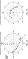
- Figure 6A illustrates the a*b* values in the CIELa*b* color space for the first example of the optical structure 10 having parameters as described in Table 1 for different viewing angles between 0 degrees and 45 degrees with respect to the normal to the surface of the first example of the optical structure 10 in reflection mode. It is observed from Figure 6A that at a viewing angle of 0 degrees with respect to the normal to the surface of the first example of the optical structure 10, the first example of the optical structure 10 appears magenta to an average human eye in reflection mode. As the viewing angle increases the color reflected by the first example of the optical structure 10 shifts along the curve 601a in the direction of the arrow towards yellow.
- Figure 6B illustrates the a*b* values in the CIELa*b* color space for the second example of the optical structure 10 having parameters as described in Table 2 for different viewing angles between 0 degrees and 45 degrees with respect to the normal to the surface of the second example of the optical structure 10 in reflection mode. It is observed from Figure 6B that at a viewing angle of 0 degrees with respect to the normal to the surface of the second example of the optical structure 10, the second example of the optical structure 10 appears yellowish green to an average human eye in reflection mode. As the viewing angle increases the color reflected by the second example of the optical structure 10 shifts along the curve 601b in the direction of the arrow towards magenta.
- Figure 6C illustrates the a*b* values in the CIELa*b* color space for the third example of the optical structure 10 having parameters as described in Table7 for different viewing angles between 0 degrees and 45 degrees with respect to the normal to the surface of the third example of the optical structure 10 in reflection mode. It is observed from Figure 6C that at a viewing angle of 0 degrees with respect to the normal to the surface of the third example of the optical structure 10, the third example of the optical structure 10 appears green to an average human eye in reflection mode. As the viewing angle increases the color reflected by the third example of the optical structure 10 shifts along the curve 601c in the direction of the arrow towards blue at 35°. The transmission color moves from red to orange as the viewing angle increases to 35°. It is noted that the various reflection and transmission color curves move counterclockwise in the various a* b* plots of Figures 6A-6D and 7A-7D .
- Figure 6D illustrates the a*b* values in the CIELa*b* color space for the fourth example of the optical structure 10 having parameters as described in Table 8 for different viewing angles between 0 degrees and 45 degrees with respect to the normal to the surface of the fourth example of the optical structure 10 in reflection mode. It is observed from Figure 6D that at a viewing angle of 0 degrees with respect to the normal to the surface of the fourth example of the optical structure 10, the fourth example of the optical structure 10 appears yellow to an average human eye in reflection mode. As the viewing angle increases the color reflected by the fourth example of the optical structure 10 shifts along the curve 601d in the direction of the arrow towards grey. In transmission the color seen at zero degrees is blue moving to magenta at 35°.
- This sample is configured as a dichroic film/pigment that has a very small color shift as the angle of view changes.
- Figure 7A illustrates the a*b* values in the CIELa*b* color space for the first example of the optical structure 10 having parameters as described in Table 1 for different viewing angles between 0 degrees and 45 degrees with respect to the normal to the surface of the first example of the optical structure 10 in transmission mode. It is observed from Figure 7A that at a viewing angle of 0 degrees with respect to the normal to the surface of the first example of the optical structure 10, the first example of the optical structure 10 appears green to an average human eye in transmission mode. As the viewing angle increases the color transmitted by the first example of the optical structure 10 shifts along the curve 701a in the direction of the arrow towards violet.
- Figure 7B illustrates the a*b* values in the CIELa*b* color space for the second example of the optical structure 10 having parameters as described in Table 2 for different viewing angles between 0 degrees and 45 degrees with respect to the normal to the surface of the second example of the optical structure 10 in transmission mode. It is observed from Figure 7B that at a viewing angle of 0 degrees with respect to the normal to the surface of the second example of the optical structure 10, the second example of the optical structure 10 appears purple to an average human eye in transmission mode. As the viewing angle increases the color reflected by the second example of the optical structure 10 shifts along the curve 701b in the direction of the arrow towards green.
- Figure 7C illustrates the a*b* values in the CIELa*b* color space for the third example of the optical structure 10 having parameters as described in Table 7 for different viewing angles between 0 degrees and 45 degrees with respect to the normal to the surface of the third example of the optical structure 10 in transmission mode. It is observed from Figure 7C that at a viewing angle of 0 degrees with respect to the normal to the surface of the third example of the optical structure 10, the third example of the optical structure 10 appears red to an average human eye in transmission mode. As the viewing angle increases the color reflected by the third example of the optical structure 10 shifts along the curve 701c in the direction of the arrow towards orange.
- Figure 7D illustrates the a*b* values in the CIELa*b* color space for the fourth example of the optical structure 10 having parameters as described in Table 8 for different viewing angles between 0 degrees and 45 degrees with respect to the normal to the surface of the fourth example of the optical structure 10 in transmission mode. It is observed from Figure 7D that at a viewing angle of 0 degrees with respect to the normal to the surface of the fourth example of the optical structure 10, the fourth example of the optical structure 10 appears blue to an average human eye in transmission mode. As the viewing angle increases the color reflected by the fourth example of the optical structure 10 shifts along the curve 701d in the direction of the arrow towards magenta.
- optical structures 10 are considered to be illuminated by D65 illumination for generating the curves of Figures 6A-6D and 7A-7D .
- Figures 8A and 8B respectively illustrate the transmittance and reflectance spectra for the third example of the optical structure 10 having parameters as described in Table 7.
- the third example of the optical structure 10 has a peak transmittance at about 650 nm while the reflectance is substantially uniform in the spectral region between about 400 nm and about 600 nm and a dip around 650 nm.
- Figures 8C and 8D respectively illustrate the transmittance and reflectance spectrum for the fourth example of the optical structure 10 having parameters as described in Table 8.
- the fourth example of the optical structure 10 has a peak transmittance between about 470 nm and about 480 nm while the reflectance is substantially uniform in the spectral region between about 520 nm and about 700 nm and a dip around 470 nm.
- the optical performance of an additional fifth example of the optical structure 10 are analyzed.
- the fifth example of the optical structure 10 comprised a glass substrate, a first dielectric layer comprising CeO 2 over the substrate, a first metal layer comprising aluminum over the first dielectric layer, a second dielectric layer comprising CeO 2 over the first metal layer, a second metal layer comprising aluminum over the second dielectric layer, and a third dielectric layer comprising CeO 2 over the second metal layer.
- the thickness of various metal and dielectric layers can be configured to appear blue/violet in transmission at a viewing angle between about 0 degrees and about 40 degrees with respect to a normal to the surface of the fifth example of the optical structure 10 and yellow/green in reflection at viewing angles between 0 degrees and about 40 degrees with respect to a normal to the surface of the fifth example of the optical structure 10.
- Figures 8E and 8F respectively illustrate the transmittance and reflectance spectrum for the fifth example of the optical structure 10 discussed above.
- Figure 8G illustrates the a*b* values in the CIELa*b* color space for the fifth example of the optical structure 10 for different viewing angles between 0 degrees and 40 degrees with respect to the normal to the surface of the fourth example of the optical structure 10 in transmission mode. It is observed from Figure 8G that at a viewing angle of 0 degrees with respect to the normal to the surface of the fifth example of the optical structure 10, the fifth example of the optical structure 10 appears blue to an average human eye in transmission mode. As the viewing angle increases the color reflected by the fifth example of the optical structure 10 shifts along the curve 751a in the direction of the arrow towards violet.
- Figure 8H illustrates the a*b* values in the CIELa*b* color space for the fifth example of the optical structure 10 for different viewing angles between 0 degrees and 40 degrees with respect to the normal to the surface of the fifth example of the optical structure 10 in reflection mode. It is observed from Figure 8H that at a viewing angle of 0 degrees with respect to the normal to the surface of the fifth example of the optical structure 10, the fifth example of the optical structure 10 appears yellow to an average human eye in reflection mode. As the viewing angle increases the color reflected by the fifth example of the optical structure 10 shifts along the curve 751b in the direction of the arrow towards green.
- an optical structure that can be used as a security feature can comprise a dielectric region comprising one or more dielectric materials surrounded by a partially optically transmissive or partially reflective metal layer (e.g., partially reflective and partially transmissive metal layer).
- the optical structure can comprise a dielectric region having first and second major surfaces (e.g., top and bottom) and edges (or sides) therebetween.
- the partially reflective and partially transmissive metal layer can be disposed on the edges (or sides) in addition to being disposed on the first and second major surfaces (e.g., top and bottom).
- the dielectric region comprising the one or more dielectric materials is optical transmissive and in some configurations may be optically transparent.
- the region comprising the one or more dielectric materials is surrounded by a partially optically transmissive and partially reflective metal layer.
- the one or more dielectric materials can comprise polymer, glass, oxides (e.g., SiO 2 , TiO 2 ) or other dielectric materials.
- the dielectric region can comprise a dielectric substrate coated with a one or more dielectric materials (e.g., layers) having a refractive index equal to, less than or greater than the refractive index of the dielectric substrate.
- the dielectric region can comprise a first dielectric material (e.g., first dielectric layer) having a first refractive index surrounded by a second dielectric material (e.g., second dielectric layer) having a second refractive index.
- the second refractive index can be equal to, less than or greater than the first refractive index.
- Figures 9A and 9B illustrate different embodiments of such optical structures.
- Figure 9A schematically illustrates a cross-sectional view of an embodiment of an optical structure 70a comprising a dielectric region 30a surrounded by a partially reflective and partially transmissive metal layer 35a.
- the optical structure 70a shown in Figure 9A has a rectilinear (e.g., rectangular) cross-section.
- Figure 9B schematically illustrates a cross-sectional view of another embodiment of an optical structure 70b comprising a dielectric region 30b surrounded by a partially reflective and partially transmissive metal layer 35b.
- the optical structure 70b shown in Figure 9B has a circular cross-section.
- the dielectric region 30a and/or 30b can comprise one or more dielectric materials such as, for example, polymer, magnesium fluoride, silicon dioxide, aluminum oxide, titanium oxide, cerium oxide, any transparent oxide material, any transparent nitride material, any transparent sulfide material, glass, combinations of any of these materials or any other inorganic or organic material.
- the refractive index of the one or more dielectric materials in the dielectric region 30a and/or 30b can have a value between about 1.35 and about 2.5.
- the refractive index of the one or more dielectric materials in the dielectric region 30a and/or 30b can have a value between about 1.38 and 1.48, between about 1.48 and about 1.58, between about 1.58 and about 1.78, between about 1.75 and about 2.0, between about 2.0 and about 2.25, between about 2.25 and about 2.5, or any value in any range/sub-range defined by these values. Values outside these ranges are also possible, in some implementations.
- the dielectric region 30a and/or 30b can comprise a dielectric substrate coated with a one or more dielectric materials having a refractive index equal to, less than or greater than the refractive index of the dielectric substrate.
- the dielectric region 30a and/or 30b can comprise a first dielectric material having a first refractive index surrounded by a second dielectric material having a second refractive index.
- the second refractive index can be equal to, less than or greater than the first refractive index.
- the dielectric region 30a and/or 30b can be configured as a slab, flake, a sphere, spheroid, ellipsoid, disc, or any other 3-dimensional shape enclosing a volume.
- the dielectric region 30a and/or 30b may have a regular or irregular shape.
- the dielectric region 30a can be configured as a slab having two major surfaces 31a and 31b and one or more edge surfaces disposed between the two major surfaces 31a and 31b. In some implementations, a number of edges surfaces may be disposed between the two major surfaces 31a and 31b.
- the number of edge surfaces may, for example, be one, two, three, four, five, six, seven, eight, nine, ten, twelve, twenty, thirty, fifty, etc. or in any range between any of these values. Values outside these ranges are also possible.
- the major surfaces 31a and 31b can have a variety of shapes. For example, one or both of the major surfaces 31a and 31b can have a rectilinear or curvilinear shape in certain implementations. The shape may be regular or irregular in certain implementations.
- one or both of the major surfaces 31a and 31b can have a square shape, a rectangular shape, a circular shape, an oval shape, an elliptical shape, pentagonal shape, a hexagonal shape, an octagonal shape or any polygonal shape.
- one or both of the major surface 31a and 31b can have jagged edges such that the lateral dimensions (e.g., length or width) of the one or both of the major surface 31a and 31b varies across the area of the one or both of the major surface 31a and 31b.
- Other configurations are also possible. Additionally, other shapes are also possible.
- One or more of the edge surfaces can have a variety of shapes (e.g., as viewed from the side), such as, for example, a square shape, a rectangular shape, an oval shape, an elliptical shape, a pentagonal shape, a hexagonal shape, an octagonal shape or any a polygonal shape.
- the shape of the one or more of the edge surfaces can be rectilinear or curvilinear in certain implementations.
- the shape may be regular or irregular in certain implementations.
- the cross-section through the dielectric region 30a and/or 30b parallel to one of the major surfaces 31a and 31b can be rectilinear or curvilinear in certain implementations and can be regular or irregular in certain implementations.
- the cross-section can have a square shape, a rectangular shape, a circular shape, an oval shape, an elliptical shape, pentagonal shape, a hexagonal shape, an octagonal shape or any a polygonal shape.
- Other shapes are also possible.
- the cross-section through the dielectric material or region 30a and/or 30b perpendicular to one of the surfaces 31a and 31b can be rectilinear or curvilinear in certain implementations and can be regular or irregular implementations.
- the cross-section can have a square shape, a rectangular shape, a circular shape, an oval shape, an elliptical shape, pentagonal shape, a hexagonal shape, an octagonal shape or any a polygonal shape. Other shapes are also possible.
- an area, a length and/or a width of the major surfaces 31a and 31b of the dielectric region 30a can be greater than or equal to about 2, 3, 4, 5, 6, 8, or 10 times the thickness of the dielectric region 30a and less than or equal to about 50 times the thickness of the dielectric region 30a, or any value in a range/sub-range between any of these values. Accordingly, the dielectric region 30a can have a large aspect ratio.
- a thickness (T) of the dielectric region 30a can correspond to the distance between the two major surfaces 31a and 31b along a vertical direction as shown in Figure 9A .
- the dielectric material 30b can be configured as a sphere.
- a thickness of the dielectric material 30b configured as a sphere can correspond to the diameter of the sphere.
- the dielectric material 30a and/or 30b can be configured as a cube, a rectangular cuboid, a cylinder, an ellipsoid, an ovoid or any other three-dimensional shape.
- the shape may be curvilinear or rectilinear in certain implementations.
- the shape may be regular or irregular in certain implementations.
- the dielectric region 30a and/or 30b can be configured as an irregularly shaped object enclosing a volume of one or more dielectric materials.
- the dielectric region 30a and/or 30b can have a thickness that allows light incident on one side of the metal layer 35a and/or 35b to constructively or destructively interfere.
- the thickness of the dielectric region 30a and/or 30b can be approximately a quarter wavelength of light (e.g., visible light) incident thereon or an integer multiple of a quarter wavelength.
- the thickness of the dielectric region 30a and/or 30b may be, for example, 1/4, 3/4, 5/4, 7/4, 9/4, 10/4, etc.
- color light is reflected by and/or transmitted through the optical structure when white light is incident thereon.
- a first color is reflected and a second different color is transmitted when white light is incident on the optical structure.
- the first color and the second color can be complementary.
- a thickness (or lateral dimension) of the dielectric region 30a and/or 30b can have a value between about 90 nm and about 2 microns. In various implementations, a thickness (or lateral dimension) of the dielectric region 30a and/or 30b can be greater than or equal to about 90 nm and less than or equal to about 1 microns, greater than or equal to about 100 nm and less than or equal to about 1.0 microns, greater than or equal to about 300 nm.
- 1.0 microns greater than or equal to about 400 nm and less than or equal to about 900 nm, greater than or equal to about 500 nm and less than or equal to about 800 nm, greater than or equal to about 600 nm and less than or equal to about 700 nm, or any thickness in any range/sub-range defined by these values. Values outside these ranges are also possible, in some implementations.
- the dielectric material 30a and/or 30b can be purchased from various suppliers (e.g., Tyndall Institute, Glassflake, Ltd., Sigma Technologies) or custom made by synthesizing in a laboratory or a manufacturing facility.
- the optical structure 70a (or 70b) and/or the dielectric region 30a (or 30b) can comprise flakes (e.g., glass flakes available from Glassflake, Ltd. http://www.glassflake.com/pages/home ).
- the flakes can comprise glass such as, for example, borosilicate flakes having an average thickness between about 90 nm and about 2 microns (e.g., an average thickness of about 1.2 microns) that may or may not be coated with coatings (e.g., high refractive index metal oxides such as TiO 2 and/or silica).
- coatings e.g., high refractive index metal oxides such as TiO 2 and/or silica.
- lateral dimensions (e.g., length and a width) of the flakes can be between about 5 microns and about 20 microns. Values outside these ranges are also possible, in some implementations.
- the dielectric region 30a or 30b can be surrounded by a partially reflective and a partially transmissive metal layer 35a or 35b.
- the metal layer 35a or 35b can comprise a metal having a ratio of the real part (n) of the refractive index to the imaginary part (k) of the refractive index (k) that is less than 1 as discussed above.
- the metal layer 35a or 35b can comprise metals that have an n/k value between about 0.01 and about 0.6, between about 0.015 and about 0.6, between about 0.01 and about 0.5, between about 0.01 and about 0.2, between about 0.01 and about 0.1, or any value in a range or sub-range defined by these values. Values outside these ranges are also possible, in some implementations.
- the metal layer 35a or 35b can comprise silver, silver alloys, gold, aluminum or copper and their respective alloys, nickel (Ni) and palladium (Pd).
- a thickness of the metal layer 35a or 35b can be configured such that the metal layer 35a or 35b is at least partially transmissive and partially reflective to light in the visible spectral region between about 400 nm and about 800 nm.
- the thickness of the metal layer 35 can be configured such that the metal layer 35a or 35b is at least partially transmissive to light in a wavelength range between about 400 nm and about 500 nm, between about 430 nm and about 520 nm, between about 450 nm and about 530 nm, between about 520 nm and about 550 nm, between about 540 nm and about 580 nm, between about 550 nm and about 600 nm, between about 600 nm and about 680 nm, between about 630 nm and about 750 nm, or any wavelength in a range/sub-range defined by any of these values.
- the thickness of the metal layer 35a or 35b can be configured such that the metal layer 35a or 35b is at least partially reflective to light in a wavelength range between about 400 nm and about 500 nm, between about 430 nm and about 520 nm, between about 450 nm and about 530 nm, between about 520 nm and about 550 nm, between about 540 nm and about 580 nm, between about 550 nm and about 600 nm, between about 600 nm and about 680 nm, between about 630 nm and about 750 nm, or any wavelength in a range/sub-range defined by any of these values. Values outside these ranges are also possible, in some implementations.
- the thickness of the metal layer 35a or 35b can vary depending on the type of metal.
- the thickness of the metal (e.g., silver) layer 35a or 35b can be greater than or equal to about 10 nm and less than or equal to about 35 nm such that the metal (e.g., silver) layer 35a or 35b can be partially transmissive to light in the visible spectral range.
- the thickness of the metal layer 35a or 35b can be less than about 10 nm or greater than about 35 nm depending possibly on the type of metal used and the wavelength range in which transmissivity or transmittance is desired.
- the metal layer 35a or 35b can have a thickness greater than or equal to about 3 nm and less than or equal to about 40 nm. Values outside these ranges are also possible, in some implementations.
- the thickness of the metal layer 35a or 35b and the dielectric region 30a or 30b can be configured such that interference of some or all of the incident light reflected by the metal layer 35a or 35b and the one or more layers of the dielectric region 30a or 30b can produce a node at or in the metal layer 35a or 35b. Accordingly, the transmittance through the metal layer 35a or 35b can be greater than the transmittance expected for a certain thickness of the metal layer 35a or 35b.
- the optical structure 70a or 70b may in some implementation, be configured to exhibit a first color in reflection mode and a second color in transmission mode.
- the dielectric region 30a or 30b can have one or more outer surfaces.
- the metal layer 35a or 35b can cover or substantially cover all the outer surfaces of the dielectric region 30a or 30b or a fraction thereof. Accordingly, in various implementations, the metal layer 35a or 35b can be disposed over at least 50% of the one or more outer surfaces of the dielectric region 30a or 30b.
- metal layer 35a or 35b can be disposed over at least 50%, over at least 60%, at least 75%, at least 80%, at least 85%, at least 90%, at least 95%, at least 99%, 100%, or any range between any of these values of the one or more outer surfaces of the dielectric region 30a or 30b.
- the metal layer 35a or 35b can be disposed over the entire area (e.g., 100%) of the one or more outer surfaces of the dielectric region 30a or 30b.
- the optical properties of the optical structure 70a or 70b can vary based on the amount of outer surface of the dielectric region 30a or 30b that is covered by the metal layer 35a or 35b.
- the reflectivity or reflectance and/or the transmissivity or transmittance of the optical structure 70a or 70b can vary based on the amount of outer surface of the dielectric region 30a or 30b that is covered by the metal layer 35a or 35b.
- the shape of the metal layer 35a or 35b can conform to the shape of the underlying dielectric material 30a or 30b.
- the dielectric material 30a has a rectangular cross-section.
- the metal layer 35a which is disposed over the major surfaces 31a and 31b and the edge surfaces also has a rectangular cross-section.
- the dielectric material 30b has a circular cross-section.
- the metal layer 35b which is disposed over the circumference of the dielectric material 30b also has a circular cross-section.
- the shape of the metal layer 35a or 35b can be different from the shape of the underlying dielectric material 30a or 30b.
- the optical structure 70a or 70b comprising a dielectric region 30a or 30b surrounded by a metal layer 35a or 35b can be configured as particles, slabs, filaments, flakes, beads (e.g., spherical beads) or platelets as discussed above.
- the optical structure 70a or 70b comprising a dielectric region 30a or 30b surrounded by a metal layer 35a or 35b can have the same shape as the shape of the dielectric region 30a or 30b.
- the optical structure 70a can be configured as a cube or a rectangular cuboid when the dielectric region 30a is configured as a cube or a rectangular cuboid as shown in Figure 9A .
- the optical structure 70b can be configured as a sphere when the dielectric region 30b is configured as a sphere as shown in Figure 9B .
- the optical structure 70a or 70b configured as a particle, a slab, a flake, a filament, or a platelet can be suitable for a pigment or a printing ink.
- the optical structure 70a or 70b configured as a particle, a slab, a flake, a filament, or a platelet can have an area (or a lateral dimension) that is about 5 to 10 times or more the thickness of the optical structure 70a or 70b configured as a particle, a slab, a flake, a filament, or a platelet.
- an optical structure 70a or 70b configured as a particle, a slab, a flake, a filament, or a platelet can have a thickness between about 100 nm and about 1 micron.
- the area (or a lateral dimension) can be greater than or equal to about 500 nm and less than or equal to about 1 micron, greater than or equal to about 1 micron and less than or equal to about 5 microns, greater than or equal to about 5 microns and less than or equal to about 10 microns, greater than or equal to about 5 micron and less than or equal to about 40 microns, greater than or equal to about 5 microns and less than or equal to about 20 microns, or any value in the ranges/sub-ranges defined by these values.
- the optical structure 70a or 70b configured as a particle, a slab, a flake, a filament, or a platelet can be configured such that an area, a length and/or a width of a major surface of the optical structure 70a or 70b is greater than or equal to about 2, 3, 4, 5, 6, 8, or 10 times the thickness of the optical structure 70a or 70b and less than or equal to about 50 times the thickness of the optical structure 70a or 70b or any value in any range formed by any of these values.
- surrounding the dielectric region 30a or 30b with the metal layer 35a or 35b can advantageously increase the reflectivity or reflectance of the dielectric material 30a or 30b at one or more wavelengths of the visible spectral range in some implementations. In some implementations, surrounding the dielectric material 30a or 30b with the metal layer 35a or 35b can advantageously enhance or change the color appearance of the dielectric material 30a or 30b at one or more wavelengths of the visible spectral range in reflection and transmission mode.
- the optical structure 70a or 70b comprising the dielectric region 30a or 30b surrounded by the metal layer 35a or 35b can have a reflection spectrum with one or more reflection peaks in the visible spectral region and a transmission spectrum with one or more transmission peaks in the visible spectral region. Without any loss of generality, the one or more reflection peaks and the one or more transmission peak do not overlap with each other. Accordingly, the optical structure 70a or 70b comprising the dielectric region 30a or 30b surrounded by the metal layer 35a or 35b can have a first color in the reflection mode and a second color different from the first color in the transmission mode. In certain implementations, the first color and the second color can be complementary colors, such as, for example, red and green, yellow and violet, blue and orange, green and magenta, etc.
- the first angle can have a value between 0 degrees and 10 degrees (e.g., 0 degrees, 1 degree, 2 degrees, 3 degrees, 4 degrees, 5 degrees, 6 degrees, 7 degrees, 8 degrees, 9 degrees or 10 degrees).
- the second angle can have a value between 20 degrees and 90 degrees (e.g., 20 degrees, 30 degrees, 40 degrees, 50 degrees, 60 degrees, 70 degrees, 80 degrees or 90 degrees).
- the color of the optical structure 70a or 70b in the reflection mode and/or the transmission mode may remain substantially the same.
- the first angle can have a value between 0 degrees and 10 degrees (e.g., 0 degrees, 1 degree, 2 degrees, 3 degrees, 4 degrees, 5 degrees, 6 degrees, 7 degrees, 8 degrees, 9 degrees or 10 degrees).
- the second angle can have a value between 20 degrees and 90 degrees (e.g., 20 degrees, 30 degrees, 40 degrees, 50 degrees, 60 degrees, 70 degrees, 80 degrees or 90 degrees) depending on the design.
- the viewing angle changes from a first angle (e.g., 0 degrees, 1 degree, 2 degrees, 3 degrees, 4 degrees, 5 degrees, 6 degrees, 7 degrees, 8 degrees, 9 degrees or 10 degrees) with respect to a normal to the surface of the optical structure 70a or 70b to a second angle with respect to a normal to the surface of the optical structure 70a or 70b and a second angle (e.g., 20 degrees, 30 degrees, 40 degrees, 50 degrees, 60 degrees, 70 degrees, 80 degrees or 90 degrees) with respect to a normal to the surface of the optical structure 70a or 70b
- the color of the optical structure 70a or 70b in the reflection mode and/or the transmission mode may change (e.g., dark blue to light blue, purple to pink, dark green to light green, etc.).
- the one or more reflection peaks of the reflection spectrum of the optical structure 70a or 70b comprising the dielectric region 30a or 30b surrounded by the metal layer 35a or 35b can have high reflectivity or reflectance.
- the reflectivity or reflectance of the one or more reflection peaks can be greater than or equal to 30%, greater than or equal to 40%, greater than or equal to 50%, greater than or equal to 55%, greater than or equal to 60%, greater than or equal to 65%, greater than or equal to 70%, greater than or equal to 75%, greater than or equal to 80%, greater than or equal to 85%, greater than or equal to 90%, greater than or equal to 95% and less than or equal to 100%, or a value in any range/sub-range defined by these values.
- the one or more transmission peaks of the transmission spectrum of the optical structure 70a or 70b comprising the dielectric region 30a or 30b surrounded by the metal layer 35a or 35b can have high transmissivity or transmittance.
- the transmissivity or transmittance of the one or more transmission peaks can be greater than or equal to 30%, greater than or equal to 40%, greater than or equal to 50%, greater than or equal to 55%, greater than or equal to 60%, greater than or equal to 65%, greater than or equal to 70%, greater than or equal to 75%, greater than or equal to 80%, greater than or equal to 85%, greater than or equal to 90%, greater than or equal to 95% and less than or equal to 100%, or a value in any range/sub-range defined by these values.
- optical structures 70a and 70b comprising the dielectric region 30a or 30b surrounded by the metal layer 35a or 35b can produce many or all the optical effects that are described above with reference to optical structure 10 where the two metal layers 13 and 15 do not surround the dielectric layer 14 (e.g., as shown in Figure 1 ).
- the metal layer 35a or 35b can be disposed around the dielectric material 30a or 30b using a variety of chemical methods.
- metal layer 35a or 35b can be disposed around the dielectric region 30a or 30b using electroless method.
- Various implementations of an electroless method of depositing the metal layer 35a or 35b can comprise depositing the metal layer 35a or 35b without applying electrical current or voltage.
- Various metals such as, for example, gold, silver, or nickel can be deposited using electroless methods.
- An example of depositing metal layer 35a or 35b comprising silver around the dielectric region 30a or 30b using an electroless method is discussed below.
- the electroless method of depositing silver can also be referred to as electroless silver plating.
- Electroless silver plating comprises immersing the dielectric region 30a or 30b in a silvering bath comprising chemical compounds of silver (e.g., silver nitrate, silver-ammonia compounds, sodium argento cyanide, etc.) and at least one of ammonia, water, potassium hydroxide or sodium hydroxide.
- the chemical compounds of silver are reduced to metallic silver using a reducing agent which is added to the silvering bath.
- the metallic silver adheres to the exposed surfaces of the dielectric region 30a or 30b.
- the reducing agent can comprise glucose, sucrose, invert sugar, stannous chloride, hydrazine, Rochelle salt, formaldehyde, or organic borane (e.g., dimethylamine borane in various implementations).
- the silvering bath and the reducing agent can be sprayed on the dielectric region 30a or 30b.
- the outer surface of the dielectric region 30a or 30b can be activated using stannous chloride (SnCl 2 ) in preparation for the electroless deposition of the metal layer.
- SnCl 2 stannous chloride
- Other methods of depositing the metal layer 35a or 35b on the outer surface of the dielectric region 30a or 30b can also be used.
- the metal layer 35a or 35b can be disposed around the dielectric region 30a or 30b using methods such as, for example, chemical vapor deposition (CVD), sputtering or electroplating.
- the metal layer 35a or 35b can be patterned around the dielectric region 30a or 30b.
- a second dielectric region 40a or 40b comprising one or more dielectric materials may be disposed around the metal coated dielectric region 30a or 30b.
- the second dielectric region 40a or 40b may comprise high refractive index materials such as ZrO 2 , TiO 2 , ZnS, ITO (indium tin oxide), CeO 2 or Ta 2 O 3 .
- the second dielectric region 40a or 40b may comprise dielectric materials having refractive index greater than 1.65 and less than or equal to 2.5.
- the refractive index of the one or more dielectric material in the second dielectric region 40a or 40b can be greater than or equal to 1.65 and less than or equal to 1.75, greater than or equal to 1.75 and less than or equal to 1.85, greater than or equal to 1.85 and less than or equal to 1.95, greater than or equal to 1.95 and less than or equal to 2.05, greater than or equal to 2.0 and less than or equal to 2.2, greater than or equal to 2.1 and less than or equal to 2.3, greater than or equal to 2.25 and less than or equal to 2.5, or any value in any range/sub-range defined by these values. Other values outside these ranges are also possible in some implementations.
- the refractive index of the one or more materials of the second dielectric region 40a or 40b can be greater than the refractive index of the one or more materials of the dielectric region 30a or 30b.
- the thickness of the second dielectric region 40a or 40b can be between 75 nm and 700 nm.
- the thickness of the second dielectric region 40a or 40b can be greater than or equal to 75 nm and less than or equal to 100 nm, greater than or equal to 100 nm and less than or equal to 150 nm, greater than or equal to 150 nm and less than or equal to 200 nm, greater than or equal to 200 nm and less than or equal to 250 nm, greater than or equal to 300 nm and less than or equal to 350 nm, greater than or equal to 400 nm and less than or equal to 450 nm, greater than or equal to 450 nm and less than or equal to 500 nm, greater than or equal to about 500 nm and less than or equal to 650 nm, greater than or equal to 650 nm and less than or equal to 700 nm, or any value in any range/sub-range defined by these values.
- the second dielectric region 40a or 40b can be disposed to cover at least 50% of the outer surface of the metal layer 35a or 35b.
- the second dielectric region 40a or 40b can be disposed to cover at least 80%, at least 90%, at least 95%, or 100% of the outer surface of the metal layer 35a or 35b, or any value in a range/sub-range defined by these values.
- the reflected color and/or the transmitted color of the optical structure 70a or 70b comprising the second dielectric region 40a or 40b surrounding the metal coated dielectric region 30a or 30b can be different from the reflected color and/or the transmitted color of the optical structure 70a or 70b comprising only the metal coated dielectric region 30a or 30b.
- the reflected color and/or the transmitted color of the optical structure 70a or 70b comprising the second dielectric region 40a or 40b surrounding the metal coated dielectric region 30a or 30b can be more vibrant than the reflected color and/or the transmitted color of the optical structure 70a or 70b comprising the metal coated dielectric region 30a or 30b without the second dielectric region 40a or 40b having suitable thickness and/or materials with suitable refractive index.
- the shape of the transmission and/or reflection peaks, the position of the maximum of the transmission and/or reflection peaks and/or the width (e.g., full width at half maximum (FWHM)) of the transmission and/or reflection peaks of the optical structure 70a or 70b comprising the second dielectric region 40a or 40b surrounding the metal coated dielectric region 30a or 30b can be different from the shape of the transmission and/or reflection peaks, the position of the maximum of the transmission and/or reflection peaks and/or the width of the transmission and reflection peaks of the optical structure 70a or 70b comprising the metal coated dielectric region 30a or 30b without the second dielectric region 40a or 40b having suitable thickness and/or materials with suitable refractive index.
- FWHM full width at half maximum
- the width of one or more of the reflection peaks of the optical structure 70a or 70b comprising the second dielectric region 40a or 40b surrounding the metal coated dielectric region 30a or 30b can be broader than the width of a corresponding reflection peak of the optical structure 70a or 70b comprising the metal coated dielectric region 30a or 30b without the second dielectric region 40a or 40b having suitable thickness and/or materials with suitable refractive index.
- the width (e.g., FWHM) of one or more of the reflection peaks of the optical structure 70a or 70b comprising the second dielectric region 40a or 40b surrounding the metal coated dielectric region 30a or 30b can be greater than or equal to about 50 nm and less than or equal to about 300 nm, in some implementations.
- Various implementations of the of the optical structure 70a or 70b comprising the second dielectric region 40a or 40b surrounding the metal coated dielectric region 30a or 30b can have a reflection spectrum with one or more reflection peaks having a width (e.g., FWHM) greater than or equal to about 10 nm, greater than or equal to about 20 nm, greater than or equal to about 30 nm, greater than or equal to about 40 nm, greater than or equal to about 50 nm, greater than or equal to about 60 nm, greater than or equal to about 70 nm, greater than or equal to about 100 nm, greater than or equal to about 200 nm, less than or equal to about 300 nm, less than or equal to about 250 nm, or any value in a range/sub-range defined by these values.
- FWHM width
- optical structure 70a or 70b comprising the second dielectric region 40a or 40b surrounding the metal coated dielectric region 30a or 30b can have higher reflectivity or reflectance at one or more wavelengths in the visible spectral range as compared to the reflectivity or reflectance of the optical structure 70a or 70b comprising the metal coated dielectric region 30a or 30b without the second dielectric region 40a or 40b having suitable thickness and/or materials with suitable refractive index at those one or more wavelengths in the visible spectral range.
- Various implementations of the of the optical structure 70a or 70b comprising the second dielectric region 40a or 40b surrounding the metal coated dielectric region 30a or 30b can have a transmission spectrum with one or more transmission peaks having a width (e.g., FWHM) greater than or equal to about 10 nm, greater than or equal to about 20 nm, greater than or equal to about 30 nm, greater than or equal to about 40 nm, greater than or equal to about 50 nm, greater than or equal to about 60 nm, greater than or equal to about 70 nm, greater than or equal to about 100 nm, greater than or equal to about 200 nm, less than or equal to about 300 nm, less than or equal to about 250 nm, or any value in a range/sub-range defined by these values.
- FWHM width
- the one or more reflection peaks of the reflection spectrum of the optical structure 70a or 70b comprising the second dielectric region 40a or 40b surrounding the metal coated dielectric region 30a or 30b can have high reflectivity or reflectance.
- the reflectivity or reflectance of the one or more reflection peaks can be greater than or equal to 30%, greater than or equal to 40%, greater than or equal to 50%, greater than or equal to 55%, greater than or equal to 60%, greater than or equal to 65%, greater than or equal to 70%, greater than or equal to 75%, greater than or equal to 80%, greater than or equal to 85%, greater than or equal to 90%, greater than or equal to 95% and less than or equal to 100%, or a value in any range/sub-range defined by these values.
- the one or more transmission peaks of the transmission spectrum of the optical structure 70a or 70b comprising the second dielectric region 40a or 40b surrounding the metal coated dielectric region 30a or 30b can have high transmissivity or transmittance.
- the transmissivity or transmittance of the one or more transmission peaks can be greater than or equal to 30%, greater than or equal to 40%, greater than or equal to 50%, greater than or equal to 55%, greater than or equal to 60%, greater than or equal to 65%, greater than or equal to 70%, greater than or equal to 75%, greater than or equal to 80%, greater than or equal to 85%, greater than or equal to 90%, greater than or equal to 95% and less than or equal to 100%, or a value in any range/sub-range defined by these values.
- the second dielectric region 40a or 40b can advantageously insulate the metal layer 35a or 35b from the ink varnish when the optical structures 70a or 70b are configured as pigments.
- the second dielectric region 40a or 40b can be disposed around the metal coated dielectric materials 30a or 30b using a sol-gel process.
- the metal coated dielectric materials 30a or 30b can be coated with a dielectric material comprising titanium di-oxide (TiO 2 ) using a sol-gel process, involving the hydrolysis of titanium(IV) isopropoxide.
- a precursor comprising the dielectric material 40a or 40b is transformed to form a colloidal suspension (or a "sol") by a series of hydrolysis and polymerization reactions.
- the colloidal suspension comprising the dielectric material of the second dielectric region 40a or 40b can be disposed on the metal coated first dielectric region 30a or 30b by a coating, gelling or precipitation.
- the metal coated first dielectric region 30a or 30b comprising the colloidal suspension comprising the dielectric material of the second dielectric region 40a or 40b can be heated or dried to obtain the metal coated first dielectric region 30a or 30b coated with second dielectric region 40a or 40b.
- the one or more materials of the second dielectric region 40a or 40b can be disposed around the metal coated first dielectric region 30a or 30b using deposition methods such as, for example, chemical vapor deposition method, e-beam, sputtering.
- the various deposition methods can be combined with vibrating the metal coated first dielectric region 30a or 30b.
- the optical structures 10, 70a or 70b are configured to partially reflect light and partially transmit light.
- the reflectivity or reflectance of the optical structures 10, 70a or 70b at one or more wavelengths in the visible spectral range can be greater than or equal to 10%, greater than or equal to 20%, greater than or equal to 30%, greater than or equal to 40%, greater than or equal to 50%, greater than or equal to 60%, greater than or equal to 70%, greater than or equal to 80%, greater than or equal to 90%, greater than or equal to 95% and/or less than or equal to 100%, or any value in any range/sub-range defined by these value.
- the transmissivity or transmittance of the optical structures 10, 70a or 70b at one or more wavelengths in the visible spectral range can be greater than or equal to 10%, greater than or equal to 20%, greater than or equal to 30%, greater than or equal to 40%, greater than or equal to 50%, greater than or equal to 60%, greater than or equal to 70%, greater than or equal to 80%, greater than or equal to 90%, greater than or equal to 95% and/or less than or equal to 100%, or any value in any range/sub-range defined by these value.
- the reflectivity or reflectance of the optical structures 10, 70a or 70b at one or more first set of wavelengths can be approximately equal to the transmissivity or transmittance of the optical structures 10, 70a or 70b at one or more second set of wavelengths different from the first set of wavelengths.
- the optical structures 10, 70a or 70b can have a size, such as, for example, a lateral dimension, an area, a length or a width of the optical structure (e.g., a length, a width or an area of a major surface of the optical structure) greater than or equal to about 1 micron and less than or equal to about 50 microns.
- a size such as, for example, a lateral dimension, an area, a length or a width of the optical structure (e.g., a length, a width or an area of a major surface of the optical structure) greater than or equal to about 1 micron and less than or equal to about 50 microns.
- the size of the optical structures 10, 70a or 70b can be greater than or equal to about 1 micron and less than or equal to 10 microns, greater than or equal to 2 microns and less than or equal to 12 microns, greater than or equal to 3 microns and less than or equal to 15 microns, greater than or equal to 4 microns and less than or equal to 18 microns, greater than or equal to 5 microns and less than or equal to 20 microns, greater than or equal to 10 microns and less than or equal to 20 microns, greater than or equal to 15 microns and less than or equal to 25 microns, greater than or equal to 20 microns and less than or equal to about 30 microns, greater than or equal to 25 microns and less than or equal to 35 microns, greater than or equal to 30 microns and less than or equal to 40 microns, greater than or equal to 35 microns and less than or equal to 45 microns, greater than or equal to 40 microns and less than or equal to 50 micro
- the optical structures 10, 70a or 70b can have a size, such as, for example, a lateral dimension, an area, a length or a width of the optical structure (e.g., a length, a width or an area of a major surface of the optical structure) greater than or equal to about 1 micron and less than or equal to about 50 microns can be between 0.1 microns and 2.0 microns.
- the thickness of the optical structures 10, 70a or 70b having a size such as, for example, a lateral dimension, an area, a length or a width of the optical structure (e.g., a length, a width or an area of a major surface of the optical structure) greater than or equal to 0.1 micron and less than or equal to 0.3 microns, greater than or equal to 0.2 microns and less than or equal to 0.5 microns, greater than or equal to 0.3 microns and less than or equal to 0.6 microns, greater than or equal to 0.4 microns and less than or equal to 0.7 microns, greater than or equal to 0.5 microns and less than or equal to 0.8 microns, greater than or equal to 0.6 microns and less than or equal to 0.9 microns, greater than or equal to 0.7 microns and less than or equal to 1.0 micron, greater than or equal to 1.0 micron and less than or equal to 1.2 microns, greater than or equal to 1.2 microns, greater than
- optical structures 10, 70a or 70b discussed above can be incorporated with or in a document (e.g., a banknote), package, product, or other item.
- Optical products such as a film, a thread, a laminate, a foil, a pigment, or an ink comprising one or more of the optical structures 10, 70a or 70b discussed above can be incorporated with or in documents such as banknotes or other documents to verify authenticity of the documents, packaging materials, etc.
- the optical structures 70a or 70b can be configured as an ink or a pigment which is disposed on a base comprising at least one of a polymer, a plastic, a paper or a fabric.
- the base may be flexible in some implementations.
- the base comprising the ink or a pigment or pigment comprising the optical structures 70a or 70b can be cut or diced to obtain a thread or a foil.
- a plurality of optical structures 10, 70a or 70b discussed above can be incorporated in a particular optical product (e.g., ink, pigment, thread, filament, paper, security ink, security pigment, security thread, security filament, security paper, etc.).
- the shapes, sizes and/or aspect ratios of the plurality of optical structures 10, 70a or 70b discussed above that are incorporated in a particular optical product e.g., ink, pigment, thread, filament, paper, security ink, security pigment, security thread, security filament, security paper, etc.
- ink, pigment, thread, filament, paper, security ink, security pigment, security thread, security filament, security paper, etc. can vary.
- a particular optical product e.g., ink, pigment, thread, filament, paper, security ink, security pigment, security thread, security filament, security paper, etc.
- optical structures 10, 70a or 70b with different distributions of shapes, sizes and/or aspect ratios of the optical structures.
- a particular optical product e.g., ink, pigment, thread, filament, paper, security ink, security pigment, security thread, security filament, security paper, etc.
- a particular optical product e.g., ink, pigment, thread, filament, paper, security ink, security pigment, security thread, security filament, security paper, etc.
- Figure 10 shows, for example, a banknote 80 comprising a laminated film 83.
- the laminated film 83 comprises the optical structure 10, 70a or 70b.
- the laminated film 83 can be fabricated by disposing the optical structure 10, 70a or 70b over a base or support layer or substrate such as polymer base layer (e.g., a polyester film).
- the optical structure 10, 70a or 70b can be disposed over the polymer base layer by a variety of methods including but not limited to coating methods, vacuum deposition on a surface of the polymer base layer, etc.
- the optical structure 10, 70a or 70b may be disposed over a first side of the surface of the polymer base layer (e.g., polyester film).
- the laminated film 83 can be adhered to the "paper" (e.g., cellulose, cotton/linen, polymer or fabric) 81 of the banknote 80, for example, by a transparent and/or an optically clear adhesive.
- a second surface of the polymer base layer opposite the first surface of the base layer is disposed closer to the banknote paper 81 comprising the banknote and may be in contact with the adhesive.
- the adhesive can be a two component adhesive with one component disposed onto the banknote paper and the other component disposed on the second surface of the polymer base layer opposite the first surface of the base layer on which the optical structure 10, 70a or 70b is disposed.
- the banknote 80 and the laminated film 83 can be brought together for bonding.
- the laminated film 83 can also be attached to the banknote 80 using a cross-linking thermoset adhesive.
- a transparent protective barrier coating 82 e.g., UV curable cross-linked resin
- the protective barrier coating 82 can extend over the edges of the laminated film 83 onto the paper (e.g., fabric) 81 of the banknote.
- the protective barrier coating 82 can be configured to protect the laminated film 83 against corrosion, abrasive wear and liquids that may commonly come in contact with the banknote 80 without sacrificing the optical effects provided by the laminated film 83.
- the optical structure 10 can be disposed facing the protective barrier coating 82 or the adhesive layer between the laminated film 83 and the "paper" 81.
- the optical structure 10, 70a or 70b can be configured as a thread (e.g., a windowed thread) instead of a laminated film.
- a windowed thread can be manufactured by a variety of methods.
- the thread can be woven up and down within the paper and to the surface of the paper during the papermaking process.
- the windowed thread can be disposed within the paper itself so that no part of the thread reaches the surface of the banknote.
- open spaces within the paper can be provided in the regions of the paper comprising the thread.
- the thread can be fabricated by cutting a strip of the optical structure 10, for example the web, sheet, or base layer on which the layers comprising the optical structure 10 are formed and passing the strip through a bath of UV curable resin.
- the rate at which the strip is passed through the UV curable resin bath can be controlled to coat the sides and the edges of the strip uniformly.
- the strip coated with the UV curable resin can be cured to obtain the thread.
- the obtained thread comprising the optical structure 10 can be inserted (e.g., weaved) in the banknote.
- any fringe e.g., the jagged or ragged edge of the thread
- any fringe e.g., the jagged or ragged edge of the thread
- any fringe e.g., the jagged or ragged edge of the thread
- Another way to affix the optical structure 10, 70a or 70b to the banknote can include die cutting a portion of the optical structure, for example, the web, sheet, or base layer on which the layers comprising the optical structure 10, 70a or 70b are formed and applying the portion to the banknote using an adhesive.
- Various implementations of the examples of optical structure described above can be configured as a thread, a hot stamp, or a laminate and incorporated with or in a document (e.g., a banknote), package, product, or other item.
- the optical structure 10, 70a or 70b or a material (e.g., an ink, a paint or a pigment, a varnish) comprising the optical structure 10, 70a or 70b can be disposed on a base comprising at least one of a polymer, a plastic, a paper or a fabric.
- the base comprising the optical structure 10, 70a or 70b or the material comprising the optical structure 10, 70a or 70b can be cut or diced into a smaller portions having a variety of shapes and/or sizes.
- the smaller portions can be disposed on or inserted into or onto a substrate (e.g., a bank note, paper, packaging material, fabric, etc.) using various methods.
- the smaller portions can be configured as strips or threads which can be woven into the substrate.
- the smaller portions can be configured as foils which can be hot stamped on the substrate.
- the smaller portions can be laminated to the substrate using adhesives.
- Figure 11A depicts a banknote 90a having two transparent windows 91a and 92a inserted into or attached on the paper (e.g., fabric) of the banknote.
- Each window comprises the optical structure 10, 70a or 70b.
- the reflection and/or transmission spectra of the optical structure 10 of the window 91a may be configured to be different from the reflection and/or transmission spectra of the optical structure 10, 70a or 70b of the window 92a.
- a person viewing the banknote 90a will perceive a first reflected color when viewing the window 91a along a viewing direction (e.g., normal to the surface of the banknote 90a) and a second reflected color different from the first reflected color when viewing the window 92a along the viewing direction.
- the person may also perceive a third transmitted color different from the first reflected color when viewing through the window 91a along the viewing direction.
- the person may additionally perceive a fourth transmitted color different from the first, second and third colors when viewing through the window 92a along the viewing direction.
- the person upon folding the banknote 90a over itself so that the two windows 91a and 92a are at least partially aligned with respect to one another, the person will perceive a different color, different from the first, second, third and/or fourth colors in reflection and transmission modes when viewing the banknote 90a along the viewing direction.
- the person upon folding the banknote 90a over itself so that the two windows 91a and 92a are at least partially aligned with respect to one another, the person will perceive a reflected color that is a combination of the effects of the reflectivity or reflectance spectrums of the two windows 91a and 92a and a transmitted color that is a combination of the effects of the transmission spectrums of the two windows 91a and 92a. Additionally, the person can perceive color shift of the various colors seen in the reflection and transmission modes as the viewing angle changes. The amount of color shift may be different from the different windows as well as for the combination of the two windows.
- Figure 11B depicts an implementation of a security device 90b (e.g., a banknote) comprising two windows 91b and 92b (a first and a second) inserted into or attached to the surface of the security device 90b.
- the two windows 91b and 92b at least partially overlap in the overlapping region 93b.
- the two windows 91b and 92b are transparent and comprise the optical structure 10, 70a or 70b.
- the configuration (e.g., thickness or other design parameters) of the optical structures 10, 70a or 70b in the respective windows 91a and 91b can be such that the reflection and/or transmission spectra of the optical structure 10, 70a or 70b of the window 91b is different from the reflection and/or transmission spectra of the optical structure 10 of the window 92b.
- a person viewing the security device 90b along a viewing direction will perceive (i) a first reflected color when viewing the portion of the window 91b that does not overlap with the window 92b, (ii) a second reflected color different from the first color when viewing the portion of the window 92b that does not overlap with the window 91b; and (iii) a third second reflected color that is a combination of the effects of the reflectivity or reflectance spectrums of the two windows 91b and 92b when viewing the overlapping region 93b.
- a person viewing the security device 90b along a viewing direction will perceive (i) a fourth transmitted color different from the first color when viewing through the portion of the window 91b that does not overlap with the window 92b, (ii) a fifth transmitted color different from the second and the fourth color when viewing through the portion of the window 92b that does not overlap with the window 91b; and (iii) a sixth transmitted color that is a combination of the effects of the transmission spectrums of the two windows 91b and 92b when viewing through the overlapping region 93b.
- a person viewing the security device 90b can perceive color shift of the various colors seen in the reflection and transmission modes as the viewing angle changes.
- the amount of color shift may be different from the different windows.
- the two windows 91b and 92b are shown as partially overlapping in Figure 11B , the two windows 91b and 92b can be completely overlapping.
- Various implementations of the security device 90b can comprise two or more different pigments.
- the two or more different pigments can comprise optical structures 10.
- a respective optical structure of one of the two or more different pigments can have reflectance and transmittance characteristics that are different from the respective optical structure of another of the two or more different pigments.
- the two or more different pigments can partially or completely overlap with each other.
- the color perceived by a person viewing an overlapping region of the two or more different pigments can depend on a combination of the effects of the reflection/transmission spectra of the different optical structures of the two or more different pigments.
- Some implementations of the security device 90b can comprise two or more at least partially overlapping foils, films, threads or laminates comprising different optical structures.
- the color perceived by a person viewing an overlapping region of the two or more at least partially overlapping foils, films, threads or laminates can depend on a combination of the effects of the reflection/transmission spectra of the different optical structures of the two or more foils, films, threads or laminates.
- Figure 12 illustrates a side view of an object 100 with a security device comprising a main body 103 of the object and a layer 102 comprising the optical structure 10, 70a or 70b.
- the object can be a banknote.
- the main body may comprise paper comprising the banknote.
- the layer 102 can be a laminate, a thread, or a label.
- an adhesive e.g., a varnish
- the layer 102 can be adhered to the adhesive of the main body 103 using a polymeric adhesive.
- the adhesive can be applied to the layer 102 before being affixed to the main body 103.
- the layer 102 is configured as a laminate, the layer 102 can be adhered to the main body 103 using a polymer.
- the layer 102 can be adhered to the main body103 using adhesives, such as, for example optical clear adhesive and/or a cross-linking thermoset adhesive.
- the security device 100 further comprises a layer 101 comprising a message that is composed using a text, a symbol, a number or any combination thereof that is disposed on the side of the main body (e.g., paper /fabric) 103 of the object (e.g., banknote) opposite the side on which the layer 102 as shown in Figure 12 .
- the layer 101 can be disposed between the main body (e.g., paper/fabric) 103 and the layer 102 or over the layer 102.
- the layer 101 can comprise, for example, a dye, a pigment or a phosphorescent material that has the same color characteristics as the color reflected or transmitted by the optical structure 10 when viewed along a direction normal to the surface of the layer 102. Accordingly, the message is not visible to an observer (or hidden) when the security device 100 is viewed along a direction normal to the surface of the layer 102. However, when the security device 100 is tilted such that viewing angle changes, the color reflected by and/or transmitted through the optical structure 10 changes such that the message become visible to the observer.
- the layer 101 comprising a message printed with a phosphorescent material can be made visible when illuminated by UV. The resultant color of the phosphorescent material can be the combined color of the fluoresence and the dichroic color.
- Figure 13 shows the effect of changing the viewing angle in transmission of the security device 100 from 0 to about 45 degrees.
- the message comprising a combination of a number, text or a symbol is not visible in the transmission mode because the color of the text is the same as the color of the optical structure in transmission mode (e.g., orange).
- the color of the optical structure in transmission mode shifts.
- the message 203 becomes visible as the color of the optical structure in transmission mode shifts from orange to yellow as the angle of observation increases.
- the color of the message has sufficient contrast with respect to the transmitted color of the optical structure 10 so as to be visible to the observer.
- the security device 100 can be configured to operate in reverse to that described above such that for example the message is visible at normal incidence and not visible when the security device is tilted. Other variations are possible.
- the optical structures 10, 70a or 70b may be used in different forms, such as a laminate, a foil, a film, a hot stamp, a thread, pigment, ink, or paint.
- a laminate, a foil, a film, or a thread can comprise a pigment, ink or paint comprising the optical structures 10, 70a or 70b.
- a laminate may be adhered to a document, product or package using adhesive.
- a thread may be threaded or woven through an opening, for example, in the document.
- a foil can be hot stamped on the document, product or package.
- Pigment, ink, or paint may be deposited on the document, product or package or the material (e.g., paper, cardboard, or fabric) used to form the document, product, or package.
- the document, product, or package may be exposed to (e.g., contacted with) the pigment, ink, or paint to color the document, product or packages in process similar to those used for non-color shifting pigments, dyes, paints and inks.
- a plurality of optical structures 10, 70a or 70b such as described herein collected together as a pigment (as well as inks, and paints) can have similar optical characteristics as the optical structure 10, 70a or 70b configured as a film/laminate.
- optical structures 10, 70a or 70b collected together to form a pigments can exhibit as a collection of platelets or separate pieces the same optical characteristics as the bulk optical film from which the platelets were made.
- An added advantage of the optical structures 10, 70a or 70b configured as a pigment is that color can be blended according to desired specification.
- the color of the optical structure 10 can be designed by using computer software to calculate the thickness of the various layers of the optical structure 10, 70a or 70b that would provide a desired reflection and/or transmission characteristics.
- Optical structures 10, 70a or 70b that can provide specific colors can be designed using the computer software and then fabricated. Additionally, different color shifting optical structures 10, 70a or 70b that produce different colors can be included together and/or color shifting optical structures such as described herein can be combined with non-color shifting pigments or dyes to produce different colors.
- the optical structure 10, 70a or 70b can be fabricated using a variety of methods including but not limited to vacuum deposition, coating methods, etc.
- One method of fabrication of the optical structures 10 described herein uses a vacuum coater that employs batch or roll coating.
- a first transparent high index layer e.g., layer 12 or layer 16 of Figure 1
- carrier or base layer such as a sheet or web or other substrate.
- the carrier, web, base layer or substrate can comprise materials such as, for example, polyester or a polyester with release characteristics such that the optical structure can be readily separated from the web or base layer.
- a release layer between the base layer and the plurality of other optical layers the form the optical structure may be used to permit separation of the optical layers comprising the optical structure from the base layer or web.
- a first metal layer e.g., layer 13 or layer 15
- a transparent dielectric layer comprising high or low refractive index material e.g., layer 14
- a second metal layer e.g., layer 15 or layer 13
- a second transparent high index layer e.g., layer 16 or layer 12
- the various layers can be deposited in sequence in some embodiments.
- one or more intervening layers can be disposed between any of the first metal layer, the transparent dielectric layer comprising high or low refractive index material, the second metal layer, and the second transparent high index layer.
- the transparent high index layers and the dielectric layer can be deposited using electron gun while the first and the second metal layers can be deposited by using electron gun or sputtering.
- the transparent dielectric layer comprising high or low refractive index material comprises a polymer
- PML Polymer Multi-Layer
- the disclosure set forth herein describes a wide variety of structures and method but should not be considered to be limited to those particular structures or methods.
- asymmetric structures are also possible.
- dielectric layers having different characteristics e.g., thickness or material
- the metal layers need not be identical and may have different characteristics such as different thicknesses or materials.
- intervening layers may also be included. One or more such intervening layer may be include such that the optical structure is not symmetric.
- an intervening layer may be included between the dielectric layer 12 and metal layer 13 and not between that metal layer 15 and the dielectric layer 16 or vice versa.
- an intervening layer may be included between the metal layer 13 and the dielectric layer 14 and not between the dielectric layer 14 and the metal layer 15, or vice versa.
- intervening layer having different characteristics may be included on different sides of the optical structure 10.
- more intervening layers may be include on one side of the optical structure 10 than on the other side of the optical structure.
- the metal layer 13 and/or the metal layer 15 can comprise metal sub-layers.
- the metal layer 13 and/or the metal layer 15 can comprise a first metal (e.g., silver) facing the high refractive index transparent layers 12 or 16 and a second metal (e.g., gold) facing the dielectric layer 14.
- this disclosure describes applications of the structures and method describe herein to include security applications, e.g., countering successful use of counterfeit currency, documents, and products, this disclosure should not be considered to be limited to those particular applications.
- security applications e.g., countering successful use of counterfeit currency, documents, and products
- this disclosure should not be considered to be limited to those particular applications.
- such features could, for example, be used for providing an aesthetic effect, to create appealing or attractive features on products or packaging for marketing and advertisement, or for other reasons.
- Dimensions, such as, thickness, length, width of various embodiments described herein can be outside the different ranges provided in this disclosure.
- the values of refractive indices for the various materials discussed herein can be outside the different ranges provided in this disclosure.
- the values for reflectance and/or transmittance of the different structures can be outside the different ranges provided herein.
- the values for spectral widths and peak locations for the reflection and transmission spectra can be outside the different ranges provided herein.
Landscapes
- Physics & Mathematics (AREA)
- Optics & Photonics (AREA)
- General Physics & Mathematics (AREA)
- Engineering & Computer Science (AREA)
- Manufacturing & Machinery (AREA)
- Finance (AREA)
- Accounting & Taxation (AREA)
- Business, Economics & Management (AREA)
- Health & Medical Sciences (AREA)
- Ophthalmology & Optometry (AREA)
- Mechanical Engineering (AREA)
- Laminated Bodies (AREA)
- Credit Cards Or The Like (AREA)
- Optical Filters (AREA)
- Inks, Pencil-Leads, Or Crayons (AREA)
Description
- This application claims the benefit of priority of
U.S. Provisional Application No. 62/568,711 filed on October 05, 2017 - This invention was made with government support under Contract No. TEPS 16-34769 awarded by the U.S. Bureau of Engraving and Printing. The U.S. government has certain rights in the invention.
- The present application generally relates to thin interference optical structures, films, coatings and pigments for producing color in both reflection mode and transmission mode. More specifically, these structures, films, coatings, and pigments exhibit large color shifting properties with changes in both reflection and transmission potentially with a change in the angle of incidence or the viewing angle. The present invention in its various aspects is as set out in the appended claims.
- [0003.1] Examples of currently used systems can be found in the following:
Park Chul-Soon et al. "Trans-reflective colour filters based on a phase compensated etalon enabling adjustment color saturation" SCIENTIFIC REPORTS, vol.6, no. 1, 6 May 2016, XP055776139, discloses a optical structure made metal and dielectric layers, specifically an Ag-TiOz-Ag structure, and discloses how changing the thickness of the layers of said structure can effect the colour saturation of the light produces by the optical structure in both a reflection and transmission mode. - [0003.3]
WO0240599 - Color shifting features can be used as a security device (for example, on a banknote) to prevent counterfeiting. The color shifting effect produced by the color shifting materials can be easy for the common person to observe. The color shifting effect produced by the color shifting features, however, can be impractical to recreate using counterfeit copies produced by color copiers, printers and/or photographic equipment. Color copiers, printers and/or photographic equipment use pigments based on dyes having absorption and as such the printed colors can be insensitive to a change in the viewing angle. Therefore, the difference between an authentic document comprising color shifting features and a fake one can be detected by tilting the document to observe if there is a color shift. Some color shifting features that are available are opaque and exhibit a color shift for reflection mode. Additionally, counterfeiters have developed sophisticated methods that compromise the effectiveness the existing reflective color shifting features as counterfeit protection. Thus, with respect to security devices, a new security feature that is difficult to counterfeit and can be readily incorporated into an item such as a banknote is desirable.
- This application discloses and contemplates a wide variety of structures including some at least partially transmissive optical structures. Advantageously, variations of such at least partially transmissive optical structures can present a color shift in both reflection mode and transmission mode with respect to viewing angle. Also, variations of such at least partially transmissive optical structures can be integrated with documents (e.g., a banknote), packaging as well as potential other items to, for example, enhance security and/or prevent counterfeiting. Although such features described herein can be used in security applications such as reducing the incidence of counterfeiting, alternatively or in addition, such feature could be used for providing an aesthetic effect or for other reasons.
- This application contemplates documents, products, and packaging with features (e.g., security features) that provides an optical effect of changing color with angle of observation in both reflection and transmission. The color shift with respect to viewing angle in both reflection and transmission can be achieved by incorporating the at least partially transmissive optical structures in the document, product, packaging etc., as a security feature. The at least partially transmissive optical structures can be a dichroic structure. The at least partially transmissive optical structures can be in the form of a thin film coating on a flexible support or base layer such as a sheet, web or carrier. In some embodiments, the at least partially transmissive optical structures comprise a pigment. In some cases, an assembly of particles comprising the at least partially transmissive optical structures can be included in a medium and form, for example an ink. The optical effect from the assembly of particles can provide a color shift in reflection and transmission. The color in transmission may be the compliment color of the color perceived in reflection mode. In some such embodiments, each particle can comprise the same structure or similar structures.
- Some implementations of the at least partially transmissive optical structures contemplated herein can comprise at least two metal layers that sandwich at least one transparent layer between the at least two metal layers. The at least one transparent layer sandwiched between the at least two metal layers can have a refractive index that is greater than, less than or equal to 1.65. The at least partially transmissive optical structures contemplated herein can further comprise transparent layers on the other side of the at least two metal layers. The transparent layers on the side of the at least two metal layers opposite the side facing the sandwiched at least one transparent layer has a refractive index greater than or equal to 1.65. The at least two metal layers can comprise metals that have a ratio of their real (n) and imaginary (k) refractive index less than 1.0. Accordingly, the metals of the at least two metal layers can have the ratio n/k<1. Without any loss of generality, the real part n is the refractive index and indicates the phase velocity, while the imaginary part k is called the extinction coefficient and can relate to absorption. The at least two metal layers can comprise silver, silver alloys, aluminum, gold, as well as other metals or materials or combination thereof.
- Various optical structures contemplated in this application can provide color shift when viewed in reflection and transmission mode as a function of viewing angle. Hence these structures can be incorporated as security features for documents such as banknotes or other documents to verify authenticity of the documents. Structures contemplated in this application can be configured to be used as a security thread, as a laminate, as a hot stamp, as a window patch or as pigment. The laminate comprising a substrate (e.g., PET), the dichroic thin film and the protective UV cured resin can be adhered as a unit to the banknote with an adhesive. Structures contemplated in this application can be configured to be used in a printing ink. Non-shifting transparent dyes or pigments can be incorporated with the optical structures contemplated in this application to obtain new colors when viewed in reflection and transmission mode. It is further contemplated that the two or more at least partially transmissive optical structures can be disposed over each other (e.g., printed or laminated over each other) to produce unique color effects. The at least partially transmissive optical structures contemplated herein can be configured or arranged to form, include or otherwise display text, symbols, numbers or figures that appear and/or disappear in reflection or transmission as the viewing angle of the security device is changed. In other configurations, the figures, images, numbers, pictures or symbols can be viewed at substantially all angles in transmission. For example, if the figures, images, numbers, pictures or symbols are printed in black, then they can be viewed at substantially all angles in transmission. In some cases, for example text, numbers, pictures or symbols can be underprinted and/or overprinted under and/or over the at least partially transmissive optical structures using existing printing technologies.
- The at least partially transmissive optical structures can be included in or on or configured as a film, a foil, a coating, a pigment or an ink. When configured as a pigment, in some implementations, the pigment can be encapsulated with a protective layer. The protective layer can comprise SiO2. The protective layer can comprise a solution prepared using a sol-gel technology such as, for example, acid or based catalyzed tetraethylorthosilicate (TEOS) reactions for increased durability. In some cases, the protective layer can further comprise silica spheres having same or different sizes. A silane coupling agent can be bonded with the protective layer comprising silica (SiO2). The silane coupling agent can be bonded to a resin, ink or paint vehicle. The resin, ink or paint vehicle can comprise a material, such as, for example, acrylic melamine, urethanes, polyesters, vinyl resins, acrylates, methacrylate, ABS resins, epoxies, styrenes and formulations based on alkyd resins and combinations or mixtures thereof. In some implementations, the at least partially transmissive optical structures can be encapsulated, for example, with an encapsulating layer having a refractive index that matches or closely matches the refractive index of the article to which it is applied. In certain implementations, the encapsulating layer can comprise a rough surface so that particles will not tend to stick together or stick to print rollers. The encapsulating layer can comprise a UV curing polymer.
- These and other aspects of the at least partially transmissive optical structures will be apparent from their accompanying drawings and this specification.
- The at least partially transmissive optical structures disclosed herein can be used for security features included in documents, products, packages, etc., in particular, as security threads in bank notes or as a laminated strip, or as a patch or as a window. Other items such as passports, ID cards, chip cards, credit cards, stock certificates or other investment securities, vouchers, admission tickets as well as commercial packages that protect items of value such as CD's, medicinal drugs, car and aircraft parts, etc. may also be protected against counterfeiting using the concepts and embodiments described herein. Furthermore, the at least partially transmissive optical structures disclosed herein can also be used for non-security applications.
- Although some of the optical structures discussed herein can provide color shift with viewing angle, optical structures that do not exhibit color shift with change in viewing angle or produce very little color shift with change in viewing angle are also contemplated.
- The systems, methods and devices disclosed herein each have several innovative aspects, no single one of which is solely responsible for the desirable attributes disclosed herein. The invention is defined by the appended claims.
- Example embodiments will now be described in conjunction with the drawings.
-
Figure 1 schematically illustrates a side view of an optical structure configured to be used as a security feature. -
Figures 2A-1 and 2A-2 schematically illustrate side views of optical structures configured to be used as a security feature in the form of a platelet encapsulated with an encapsulating layer, comprising, for example, a SiO2 layer and silica spheres. -
Figures 2B-1 and 2B-2 illustrates a plurality of platelets dispersed in a polymer which can comprise an ink or a paint medium. -
Figure 3 illustrates the silane coupling agent bonded to an exposed surface of the encapsulation layer of a platelet. Another side of the silane coupling agent can also bond to a medium such as a polymer in which the platelets are dispersed. -
Figure 4 is a schematic illustration showing propagation light incident on the optical structure and the resultant nodes in field strength at the metal layers. -
Figures 5A and 5B illustrate transmission and reflection spectra of examples of optical structures. -
Figures 6A-6D and7A-7D are a* b* plots showing the color travel or change in reflection and transmission respectively for four different example optical structures. -
Figures 8A and 8B respectively illustrate the transmittance and reflectance spectra for an example of the optical structure. -
Figures 8C and 8D respectively illustrate the transmittance and reflectance spectrum for an example of the optical structure. -
Figures 8E and 8F respectively illustrate the transmittance and reflectance spectrum for an example of the optical structure. -
Figure 8G illustrates the a*b* values in the CIELa*b* color space for an example of the optical structure for different viewing angles between 0 degrees and 40 degrees with respect to the normal to the surface of the example of the optical structure in transmission mode. -
Figure 8H illustrates the a*b* values in the CIELa*b* color space for an example of the optical structure for different viewing angles between 0 degrees and 40 degrees with respect to the normal to the surface of the example of the optical structure in reflection mode. -
Figure 9A schematically illustrates a cross-sectional view of an embodiment of an optical structure configured to be used as a security feature.Figure 9B schematically illustrates a cross-sectional view of another embodiment of an optical structure configured to be used as a security feature. -
Figure 10 is a schematic illustration of a laminate structure comprising an optical structure that is affixed to a banknote. -
Figure 11A shows a banknote with two windows, each window including a different optical structure.Figure 11B shows a security device with two at least partially overlapping windows, each window comprising a different optical structure. -
Figures 12 and 13 illustrate examples of a security device comprising an optical structure disposed under or over a text, symbol or number. The text, symbol or number becomes visible when the viewing angle is changed. - To curtail counterfeiting, currency, documents (e.g., banknotes) as well as other items such as products and packaging can be provided with security features that can be inspected by the general public to verify authenticity. In many cases, it can be advantageous if the security features can be easily seen under a variety of light conditions and without the need for special lighting conditions. It can also be desirable that the security features have distinct characteristics that can be easily identified by the public within a 1-10 second time frame. In addition, it is advantageous in general, if the security feature is not susceptible to copying by electronic or photographic equipment, such as, for example, printers, copiers, cameras, etc.
- One example of a security feature employed in banknotes is the watermark, which has a fairly high degree of awareness among the general public. An example of a watermark can be an image comprising light and dark regions that can be easily seen by holding up the banknote to see the watermark in light transmission. However, watermarks may be susceptible to be copied and thus are not very secure. Other examples of security features may use inks and motion type features that are not readily seen under low light conditions (e.g., at low lit bars, restaurants, etc.), have poor image resolution, and/or have slow optical movement relative to the movement of the banknote. Accordingly, some existing security features tend to be more complicated structures having more complex color changing effects. This approach, however, can be disadvantageous when the complicated security devices are applied to banknotes or currency, as these complicated security devices may confuse an average person who is looking for a distinctive security feature.
- Having a security features that has high contrast with respect to the background that can be easily identified by the general public under a variety of light conditions, including low light, can be advantageous. Accordingly, various security features disclosed can appears to have one color in reflection and another different color in transmission. These security features can be incorporated in a banknote. A consumer, merchant, or a bank teller can holdup such a banknote to light to readily verify the authenticity of the banknote. Additionally, in some implementations, the security feature can be configured to exhibit color shift and/or movement of identifiable features when the viewing angle is varied to enhance security. These and other features are described in further detail herein.
- Accordingly, various security features contemplated herein can comprise optical stacks and/or structures that are at least partially reflective and at least partially transmissive. The security features contemplated herein can be configured as coatings, threads, laminates, foils, films, pigments and/or inks and incorporated with banknotes or other items. The innovative aspects described in this application also include systems and methods of fabricating optical structures and/or stacks that are at least partially reflective and at least partially transmissive. In some embodiments, such optical structures may be fabricated on support or base layers or sheets such as webs (e.g., roll coated webs). Processes described herein may also include removing the fabricated optical structures and/or stacks from a support or base layer (e.g., roll or sheet). The innovative aspects described in this application further includes methods and systems for including the optical structures and/or stacks that are at least partially reflective and at least partially transmissive in pigment and inks having a desired amount of durability and mechanical strength to be further used in or on or incorporated into banknotes and other security devices/documents.
-
Figure 1 schematically illustrates anoptical structure 10 comprising a stack of layers that can be used as a security feature. Theoptical structure 10 comprises at least twometal layers metal layers metal layers metal layers metal layers metal layer metal layer metal layer 13 can be equal to the thickness of themetal layer 15. Alternately, the thickness of themetal layer 13 can be greater than or less than the thickness of themetal layer 15. - A
transparent dielectric layer 14 is sandwiched between the at least twometal layers dielectric layer 14 can have a refractive index greater than, less than or equal to 1.65. Materials with an index greater than or equal to 1.65 can be considered as high refractive index materials for the purpose of this application and materials with an index less than 1.65 can be considered as low index materials for the purpose of this application. Thetransparent dielectric layer 14 can comprise inorganic materials including but not limited to silicone dioxide (SiO2), aluminum oxide (Al2O3), magnesium fluoride (MgF2), cerium fluoride (CeF3), lanthanum fluoride (LaF3), zinc oxide (ZnO), zinc sulfide (ZnS), zirconium dioxide (ZrOz), titanium dioxide (TiO2), tantalum pentoxide (TazOs), ceric oxide (CeO2), ytterium oxide (Y2O3), indium oxide (In2O3), tin oxide ( SnO2), indium tin oxide (ITO) and tungsten trioxide (WO3) or combinations thereof. Thetransparent dielectric layer 14 can comprise polymers including but not limited to parylene, acrylates, and/or methacrylate. Without any loss of generality, thetransparent dielectric layer 14 comprises a material having an index of refraction greater than, less than, or equal to 1.65 and an extinction coefficient between 0 and about 0.5 such that it has low absorption of light in the visible spectral range. - The
dielectric layer 14 can have a thickness that is greater than or equal to about 75 nm and less than or equal to about 2 micron. For example, thedielectric layer 14 can have a thickness that is greater than or equal to about 150 nm and less than or equal to about 650 nm, greater than or equal to about 200 nm and less than or equal to about 600 nm, greater than or equal to about 250 nm and less than or equal to about 550 nm, greater than or equal to about 300 nm and less than or equal to about 500 nm, greater than or equal to about 350 nm and less than or equal to about 450 nm, greater than or equal to about 700 nm and less than or equal to about 1 micron, greater than or equal to about 900 nm and less than or equal to about 1.1 micron, greater than or equal to about 1 micron and less than or equal to about 1.2 micron, greater than or equal to about 1.2 micron and less than or equal to about 2.0 microns or any value in a range/sub-range defined by these values. Without subscribing to any particular theory, in various implementations, the thickness of thedielectric layer 14 can be approximately a quarter wavelength of light (e.g., visible light) incident thereon or an integer multiple of a quarter wavelength. In various implementations, the thickness of thedielectric layer 14 may be, for example, 1/4, 3/4, 5/4, 7/4, 9/4, 10/4, etc. of the wavelength of visible light incident on thedielectric layer 14. - The
optical structure 10 further comprises atransparent dielectric layer 12 that is disposed on a side of themetal layer 13 that is opposite to thedielectric layer 14 and atransparent dielectric layer 16 that is disposed on a side of themetal layer 15 that is opposite to thedielectric layer 14. In some cases, layers 12 and 16 can comprise materials having a refractive index greater than or equal to 1.65. For example, layers 12 and 16 can comprise ZrO2, TiO2, ZnS, ITO (indium tin oxide), CeO2 or Ta2O3. Dielectric layers 12 and 16 can have a thickness that is greater than or equal to about 100 nm and less than or equal to about 400 nm, greater than or equal to about 150 nm and less than or equal to about 350 nm, greater than or equal to about 200 nm and less than or equal to about 300 nm, or any value in a range/sub-range defined by these values. The thickness of thedielectric layer 12 can be equal to the thickness of thedielectric layer 16. Alternately, the thickness of thedielectric layer 12 can be greater than or less than the thickness of thedielectric layer 16. Theoptical structure 10 can have a thickness that is less than or equal to about 2 microns. - Fabricating the
optical structure 10 can include providing the layer of dielectric material 12 (or the layer of dielectric material 16) and depositing the metal layer 13 (or the metal layer 15) over the layer of dielectric material 12 (or the layer of dielectric material 16). The metal layer 13 (or the metal layer 15) can be deposited over the layer of dielectric material 12 (or the layer of dielectric material 16) using an electroless method discussed in further detail below. The metal layer 13 (or the metal layer 1.5) can be deposited as a continuous thin film, as small spheres, metallic clusters or island like structures. Theother dielectric layer 14 can be subsequently disposed over the metal layer 13 (or the metal layer 15). The initial layer of dielectric material 12 (or the layer of dielectric material 16) can be disposed and/or formed over a support. The support is also referred to herein as a base layer. The support can comprise a carrier. The support can comprise a sheet such as a web. The support can comprise a substrate. The substrate can be a continuous sheet of PET or other polymeric web structure. The support can comprise a non-woven fabric. Non-woven fabrics can be flat, porous sheets comprising fibers. In some implementations, the non-woven fabric can be configured as a sheet or a web structure that is bonded together by entangling fiber or filaments mechanically, thermally, or chemically. In some implementations, the non-woven fabric can comprise perforated films (e.g., plastic or molten plastic films). In some implementations, the non-woven fabric can comprise synthetic fibers such as polypropylene or polyester or fiber glass. - The support can be coated with a release layer comprising a release agent. The release agent can be soluble in solvent or water. The release layer can be polyvinyl alcohol, which is water soluble or an acrylate which is soluble in a solvent. The release layer can comprise a coating, such as, for example, salt (NaCl) or cryolite (Na3AlF6) deposited by evaporation before the layers of the optical structure are deposited/formed.
- In some implementations of the support configured as a non-woven fabric, the non-woven fabric can be coated with a release layer. Such implementations can be dipped or immersed in a solvent or water that acts as a release agent to dissolve or remove the release layer. The release agent (e.g., the solvent or water) is configured to penetrate from a side of the non-woven fabric opposite the side on which the optical structure is disposed to facilitate release of the optical structure instead of having to penetrate through the optical structure. The optical structure is recovered from the solvent or water after dissolution of the release layer. In some manufacturing approaches, the recovered optical structure can then be processed into a pigment.
- In one method of fabrication, the
optical structure 10 can be fabricated, for example, deposited or formed on a coated web, a coated base layer, a coated carrier or a coated substrate. The coating on the web, the base layer, the substrate or the carrier can be configured as a release layer to facilitate easy removal of theoptical structure 10. - The
optical structure 10 can be configured as a film or a foil by disposing over a substrate or other support layer having a thickness, for example, greater than or equal to about 10 microns and less than or equal to about 25 microns. For example, a substrate or support layer such as a polyester substrate or support layer can have a thickness greater than or equal to 12 microns and less than or equal to 22.5 microns, greater than or equal to 15 microns and less than or equal to about 20 microns. The substrate or support layer can comprise materials, such as, for example, polyester, polyethylene, polypropylene, or polycarbonate. The support or support layer itself can be dissolvable. The support or support layer, for example, can also comprise polyvinyl alcohol, which can be dissolved, for example, in water. Accordingly, instead of using a release layer on a insoluble support web, the support web itself may comprise soluble material. Accordingly, the support or support layer can be dissolved leaving the optical coating remaining. Theoptical structure 10 configured as a film or a foil can be encapsulated with a polymer, such as, for example a UV cured polymer. - The
optical structure 10 can comprises additional layers. For example, a thin protective layer may be disposed between themetal layer 13 and thedielectric layer 12 and/or between themetal layer 15 and thedielectric layer 16. The protective layer can comprise materials, such as, for example, NiCrOx ,Si3N4, CeSnOa and ZnSnO4. The protective layers can have a thickness between about 3-5 nm. The protective layers can advantageously increase the durability of the metal layers 13 and 15. - Instead of a film, the optical structure, 10, may be removed from the substrate, web, carrier, or support layer on which it is fabricated and divided into platelets having a size that is suitable for a pigment or printing ink. Platelets having a size that is suitable for a pigment or printing ink can have an area, length, and/or width that is about 5-10 times the thickness of the platelet, in some implementations. Accordingly, the platelets having a thickness of about 1 micron, and/or can have a width and/or a length that is between approximately 5 micron and about 50 microns. For example, the width and/or a length can be greater than or equal to about 5 micron and less than or equal to about 15 microns, greater than or equal to about 5 microns and less than or equal to about 10 microns, greater than or equal to about 5 micron and less than or equal to about 40 microns, greater than or equal to about 5 microns and less than or equal to about 20 microns, or any value in the ranges/sub-ranges defined by these values. Platelets having a length and/or width that is less than about 5-10 times the thickness of the platelet, such as, for example having a length and/or width that is equal to the thickness of the platelet can be oriented along their edges in the printing ink or pigment. This can be disadvantageous since pigment or printing ink comprising platelets that are oriented along their edges may not exhibit the desired colors in reflection and transmission modes. Dimensions such as, thicknesses, lengths and/or widths outside these ranges are also possible.
-
Figure 2A-1 illustrates an example of aplatelet 20. The optical structure, 10 is fractured, cut, diced or otherwise separated to obtain the separate, for example, microns sized, pieces or platelets. In some implementations, the obtained platelets may be surrounded by anencapsulating layer 21. The encapsulatinglayer 21 can comprise a moisture resistant material, such as, for example silicon dioxide. The encapsulatinglayer 21 can also comprisesilica spheres 22 and 23. Thesilica spheres 22 and 23 can be of the same size or have different sizes. The encapsulatinglayer 21 can help protect the at least twometal layers layer 21 can additionally and/or alternatively reduce the occurrence of delamination of the at least twometal layers optical structure 10. Theoptical structures 10 surrounded by the encapsulatinglayer 21, and potentially comprising thesilica spheres 22 and 23, can be configured asplatelets 20 that are suitable for a pigment or printing ink. Thesilica spheres 22 and 23 of theencapsulating layer 21 can help prevent the platelets from adhering to one another. Without the spheres the platelets may stick together like two microscope slides stick together. Thespheres 22 and 23 can also prevent theplatelets 20 from sticking to the print rollers in the printing machine. One method of surrounding theoptical structure 10 with anencapsulating layer 21 can rely on sol-gel technology using tetraethylorthosilicate (TEOS). In one method of forming theencapsulating layer 21, an alcohol based solution of TEOS can be added in small quantities (e.g., one or more drops at a time) to a dispersion of the platelets in alcohol or water. A catalyst, such as, for example, an acid or sodium hydroxide solution can be added into the a dispersion of the platelets in alcohol or water in small quantities (e.g., one or more drops at a time). The dispersion of the platelets in alcohol or water can be heated to a temperature of about 50-70°C, while stirring to transform TEOS to a silica coating. Other processes, however, may be employed. - In some embodiments, a plurality of
platelets 20 can form a pigment. Such a pigment may be color shifting (e.g., the color reflected and/or transmitted changes with angle of view or angle of incidence of light), in some cases. In some embodiments, non-color shifting pigment or dye may be mixed with the pigment. In some embodiments other materials may be included with theplatelets 20 to form the pigment. Although some of the pigments discussed herein can provide color shift with change in viewing angle or angle of incidence of light, pigments that do not exhibit color shift with change in viewing angle or angle of incidence of light or that produce very little color shift with change in viewing angle or angle of incidence of light are also contemplated. - In some embodiments, the
platelets 20 can be added to a medium such as a polymer 25 (e.g., a polymeric resin) to form a dichroic ink, a pigment, or paint as shown inFigure 2B-1 . The platelets can be suspended in the medium (e.g., polymer) 25. The platelets can be randomly oriented in the medium (e.g., polymer) 25 as shown inFigure 2B-1 . During the printing process, in some cases, the individual platelets can be oriented parallel to the surface of the object (e.g., paper) to which the pigment, the paint, or the dichroic ink is being applied as a result of, for example, the printing action, gravity, and/or surface tension of the normal drying process of the pigment, the paint, or the dichroic ink as shown inFigure 2B-2 . The medium 25 can comprise material including but not limited to acrylic melamine, urethanes, polyesters, vinyl resins, acrylates, methacrylate, ABS resins, epoxies, styrenes and formulations based on alkyd resins and mixtures thereof. In some implementations, the medium 25, e.g., polymer, can have a refractive index that closely matches the refractive index of the encapsulatingsilica layer 21 and/or silica balls such that the encapsulating layer and/or the silica balls do not adversely affect the optical performance of the pigment, the paint, or the dichroic ink in the medium. - In various implementations, the
platelets 20 need not be surrounded by an encapsulating layer. In such implementations, one ormore platelets 20 that are not encapsulated by an encapsulating layer can be added or mixed with an ink or a pigment medium (e.g., varnish, polymeric resin, etc.) to obtain a dichroic ink or pigment as discussed above. In various implementations, the dichroic ink or pigment can comprise a plurality ofplatelets 20. Theoptical structures 10 that are configured as the plurality ofplatelets 20 can have different distributions of shapes, sizes, thicknesses and/or aspect ratios. Theoptical structures 10 that are configured as the plurality ofplatelets 20 can also have different optical properties. For example, theoptical structures 10 that are configured as the plurality ofplatelets 20 can also have different color properties. - In some implementations, an optical structure comprising only the metal layers 13 and 15 and the
transparent dielectric layer 14 without the high refractive indexdielectric layers Figure 2A-2 can be configured as platelets as discussed above and dispersed in the medium 25 as shown inFigure 2B-2 to manufacture a dichroic printing ink, paint or pigment as discussed above. In some implementations, the platelets including an optical structure comprising only the metal layers 13 and 15 and thetransparent dielectric layer 14 without the high refractive indexdielectric layers - A silane coupling agent can be bonded to the
encapsulating layer 21 to form a functionalizedplatelet 30 as shown inFigure 3 . Bonding of the silane coupling agent to the encapsulating layer can occur through a hydrolyzing reaction. The silane coupling agent can bind to the polymer (e.g., polymeric resin) of the printing ink or paint medium so that the heterogeneous mixture of pigment and the polymer do not separate during the printing process and substantially function in much the same way as a homogeneous medium would function. The printing ink or paint medium can comprise material including but not limited to acrylic melamine, urethanes, polyesters, vinyl resins, acrylates, methacrylate, ABS resins, epoxies, styrenes and formulations based on alkyd resins and mixtures thereof. The silane coupling agents used can be similar to the silane coupling agents sold by Gelest Company (Morristown, PA USA). In some implementations, the silane coupling agent can comprise a hydrolyzable group, such as, for example, an alkoxy, an acyloxy, a halogen or an amine. Following a hydrolyzing reaction (e.g., hydrolysis), a reactive silanol group is formed, which can condense with other silanol groups, for example, with the silica spheres of theencapsulating layer 21 or the encapsulating layer of silica to form siloxane linkages. The other end of the silane coupling agent comprises the R-group 31. The R-group 31 can comprise various reactive compounds including but not limited to compounds with double bonds, isocyanate or amino acid moieties. Reaction of the double bond via free radical chemistry can form bonds with the ink polymer(s) such as those based on acrylates, methacrylates or polyesters based resins. For example, isocyanate functional silanes, alkanolamine functional silanes and aminosilanes can form urethane linkages. - Without any loss of generality, in various implementations of the
optical structure 10 configured as a platelet that do not comprise the encapsulating layer, the silane coupling agent can be bonded to one or both of the high refractive indexdielectric layers - Without any loss of generality, the
optical structure 10 can be considered as an interference stack or cavity. Ambient light incident on the surface of theoptical structure 10 is partially reflected from the various layers of theoptical structure 10 as shown byrays Figure 4 and partially transmitted through the various layers of theoptical structure 10 as shown byray 49 inFigure 4. Figure 4 illustrates an embodiment of anoptical structure 10 comprising the high refractiveindex dielectric layer dielectric layer 14 encapsulated in theencapsulating layer 21. Some wavelengths of the ambient light reflected from the various layers may interfere constructively and some other wavelengths of the ambient light reflected from the various layers may interfere destructively. Similarly, some wavelengths of light transmitted through the various layers may interfere constructively and some other wavelengths of the ambient light transmitted through the various layers may interfere destructively. As a result of which, theoptical structure 10 appears colored when viewed in transmission and reflection mode. In general, the color and the intensity of light reflected by and transmitted through theoptical structure 10 can depend on the thickness and the material of the various layers of theoptical structure 10. By changing the material and the thickness of the various layers, the color and intensity of light reflected by and transmitted through theoptical structure 10 can be varied. Without subscribing to any particular scientific theory about the operation of theoptical structures 10, in general, the material and the thickness of the various layers can be configured such that some or all of the ambient light reflected by the various layers interfere such that anode 45 in thefield 42 occurs at the twometal layer node 45 in thefield 42 occurs at the twometal layer node 45 might not occur. Accordingly, in some implementations, the twometal layers metal layers transparent dielectric layer 14, a portion of the incident light may be transmitted through theoptical structure 10 as a result of the phenomenon of "induced transmittance" or "induced transmission". The reflection and transmission spectral characteristics are discussed below. -
Figure 5A shows a spectral plot in both transmission (curve 501a) and reflection (curve 503a) for a first example of theoptical structure 10. The materials of the various layers of the first example of theoptical structure 10 and the thickness of the various layers of the first example of theoptical structure 10 are provided in Table 1 below. As indicated in Table 1, the first example of theoptical structure 10 comprises two metal layers comprising silver. The two silver layers correspond to the at least twometal layer optical structure 10 shown inFigure 1 . Both the silver layers have the same thickness of 25 nm. A dielectric layer having a thickness of 300 nm is sandwiched between the two silver layers. The dielectric layer comprises SiO2 which has a refractive index of 1.47011. The dielectric layer comprising SiO2 corresponds to thetransparent layer 14 having a low refractive index (i.e., refractive index less than 1.65). A layer of ZrO2 is disposed on the side of each of the two silver layers that is opposite the side facing the SiO2 layer. Each of the two layers comprising ZrO2 has a thickness of 150 nm. As noted from Table 1 below, ZrO2 has a refractive index of 2.27413. The two layers comprising ZrO2 corresponds to thetransparent layers optical structure 10 is encapsulated in a SiO2 matrix as indicated in Table 1. The SiO2 matrix is used to simulate the printing medium or ink which has a similar refractive index. - The transmission and reflection of light observed at an angle of 0 degrees with respect to a normal to the first example of the
optical structure 10 is shown inFigure 5A . Thereflection spectrum 503a (indicated ascurve # 1 in Figure SA) and thetransmission spectrum 501a (indicated ascurve # 0 inFigure 5A ) in the spectral range between about 400 nm and about 700 nm which includes the visible spectral range were obtained using a simulation software from http;//thinfilm.hansteen.net. -
# # Slab: # SIO2 N=(1.47011 ,0) mynkdb/SIO2.NK # ZRO2 d=1.5e-07 N=(2.27413 ,0) mynkdb/ZRO2.NK # AG d-2.5e-08 N=(0.173038 ,1.94942) mynkdb/AG.NK # SIO2 d=3e-07 N=(1.47011 ,0) mynkdb/SIO2.NK # AG d=2.5e-08 N=(0.173038 ,1.94942) mynkdb/AG.NK # ZRO2 d=1.5e-07 N=(2.27413 ,0) mynkdb/ZRO2.NK # SIO2 N=(1.47011 ,0) mynkdb/SIO2.NK # # Beam: # Wavelength=(4e-07,0) Angle=0.0174533 Polarization=1 N=(1.47011,0) # # Supported spectral range: 2.5e-07m - 8.5e-07m. # # Lambda[nm] R[] # -
Table 1: Parameters of a first example of the optical structure that has the reflection and transmission spectra as shown in Figure 5A. # # Slab: # SIO2 N=(1.47011 ,0) mynkdb/SIO2.NK # ZRO2 d=1.5e-07 N=(2.27413 ,0) mynkdb/ZRO2.NK # AG d=2.5e-08 N=(0.173038 ,1.94942) mynkdb/AG.NK # SIO2 d=3e-07 N=(1.47011 ,0) mynkdb/SIO2.NK # AG d=2.5e-08 N=(0.173038 ,1.94942) mynkdb/AG.NK # ZRO2 d=1.5e-07 N=(2.27413 ,0) mynkdb/ZRO2.NK # SIO2 N=(1.47011 ,0) mynkdb/SIO2.NK # # Beam: # Wavelength=(4e-07,0) Angle=0.0174533 Polarization=1 N=(1.47011,0) # # Supported spectral range: 2.5e-07m - 8.5e-07m. # # Lambda[nm] T[ ] # - It can be seen from
Figure 5A that thetransmission curve 501a (curve#0) has a peak with a maximum value occurring at a wavelength of about 520 nm and thereflection curve 503a has two peaks with a first maximum value occurring at a wavelength of 420 nm and a second maximum value occurring at a wavelength of about 650 nm. The maximum value of the transmission and reflection peaks is greater than 0.5 which indicates that the transmission and reflection peaks have high intensities. - Furthermore, the transmission and reflection peaks have a bandwidth as measured at 50% of the maximum value of the peak greater than about 20 nm. The bandwidth as measured at 50% of the maximum value of the peak is referred to as full width at half maximum (FWHM). It is observed from
Figure 5A that the FWHM of the transmission peak is about 75 nm. - Based on the position of the transmission and reflection peaks and the bandwidth of the transmission and reflection peaks, the
optical structure 10 is perceived as having a first color in the reflection mode and a second color in the transmission mode by an average human eye. In some cases, the first color and the second color can be complimentary colors. In some cases, the transmission and reflection peaks comprising a range of wavelengths of the visible spectral range can have a high intensity and a FWHM greater than 2 nm (e.g., FWHM greater than or equal to about 10 nm, FWHM greater than or equal to about 20 nm, FWHM greater than or equal to about 30 nm, FWHM greater than or equal to about 40 nm, FWHM greater than or equal to about 50 nm, FWHM greater than or equal to about 60 nm, FWHM greater than or equal to about 70 nm, FWHM greater than or equal to about 100 nm, FWHM greater than or equal to about 200 nm, FWHM less than or equal to about 300 nm, FWHM less than or equal to about 250 nm, or any value in a range/sub-range defined by these values). - The one or more reflection peaks can be considered to have a high intensity if the reflectivity or reflectance of the peak in a range of visible wavelengths is greater than or equal to about 50% and less than or equal to about 100%. For example, the one or more reflection peaks can be considered to have a high intensity if the amount of light reflected or reflectivity or reflectance in a range of visible wavelengths is greater than or equal to about 55% and less than or equal to about 99%, greater than or equal to about 60% and less than or equal to about 95%, greater than or equal to about 70% and less than or equal to about 90%, greater than or equal to about 75% and less than or equal to about 85%, or any value in a range/sub-range defined by these values.
- The one or more transmission peaks can be considered to have a high intensity if the transmissivity or transmittance of the peak in a range of visible wavelengths is greater than or equal to about 50% and less than or equal to about 100%.
For example, the one or more transmission peaks can be considered to have a high intensity if the amount of light transmitted or transmissivity or transmittance in a range of visible wavelengths is greater than or equal to about 55% and less than or equal to about 99%, greater than or equal to about 60% and less than or equal to about 95%, greater than or equal to about 70% and less than or equal to about 90%, greater than or equal to about 75% and less than or equal to about 85%, or any value in a range/sub-range defined by these values. - The first example of the
optical structure 10 having a design as depicted in Table 1 and having a reflection spectrum and a transmission spectrum as shown inFigure 5A appears green in transmission mode and as magenta in reflection mode to an average human eye. Without any loss of generality, it can be advantageous, in various implementations, for the peaks in the reflection and transmission spectra to be non-overlapping as shown inFigures 5A and 5B such that a reflection peak having a highest possible reflectance or reflectivity can be obtained in one region of the visible spectral range and a transmission peak having a highest possible transmittance or transmissivity can be obtained in a non-overlapping region of the visible spectral range. Accordingly, the reflected color and the transmitted color can be different and potentially complementary to each other, such as, for example, red and green, yellow and violet, blue and orange, green and magenta, etc. - The shape of the transmission and reflection peaks, the position of the maximum of the transmission and reflection peaks, the FWHM of the transmission and reflection peaks, etc. can be varied by varying the materials and/or thickness of the various layers of the
optical structure 10. This can be observed fromFigure 5B which depicts thereflection spectrum 503b andtransmission spectrum 501b of a second example of theoptical structure 10 which has the same material composition as the first example of theoptical structure 10 but different thickness for the various layers. The parameters of the second example of theoptical structure 10 are provided in Table 2 below. As noted from Table 2, the thickness of the dielectric layer comprising SiO2 and having a refractive index of 1.47011 in the second example of theoptical structure 10 is 400 nm instead of 300 nm in the first example of theoptical structure 10. Furthermore, the thickness of the two ZrO2 disposed on either side of each of the two silver layers is 225 nm in the second example of theoptical structure 10 instead of 150 nm in the first example of theoptical structure 10. -
# # Slab: # SIO2 N=(1.47011 0) mynkdb/SIO2.NK # ZRO2 d=2.25e-07 N=(2.27413 0) mynkdb/ZRO2.NK # AG d=2.5e-08 N=(0.173038 ,1.94942) mynkdb/AG.NK # SIO2 d=4e-07 N=(1.47011 0) mynkdb/SIO2.NK # AG d=2.5e-08 N=(0.173038 ,1.94942) mynkdb/AG.NK # ZRO2 d=2.25e-07 N=(2.27413 0) mynkdb/ZRO2.NK # SIO2 N=(1.47011 0) mynkdb/SIO2.NK # # Beam: # Wavelength=(4e-07,0) Angle=0.0174533 Polarization=1 N=(1.47011,0) # # Supported spectral range: 2.5e-07m - 8.5e-07m. # # Lambda[nm] R[] # -
Table 2: Parameters of a second example of the optical structure that has the reflection and transmission spectra as shown in Figure 5B. # # Slab: # SIO2 N=(1.47011 0) mynkdb/SIO2.NK # ZRO2 d=2.25e-07 N=(2.27413 0) mynkdb/ZRO2.NK # AG d=2.5e-08 N=(0.173038 ,1.94942) mynkdb/AG.NK # SIO2 d=4e-07 N=(1.47011 0) mynkdb/SIO2.NK # AG d=2.5e-08 N=(0.173038 ,1.94942) mynkdb/AG.NK # ZRO2 d=2.25e-07 N=(2.27413 0) mynkdb/ZRO2.NK # SIO2 N=(1.47011 0) mynkdb/SIO2.NK # # Beam: # Wavelength=(4e-07,0) Angle=0.0174533 Polarization=1 N=(1.47011,0) # # Supported spectral range: 2.5e-07m - 8.5e-07m. # # Lambda[nm] T[] # - As a result of the change in the thickness of the dielectric layers comprising SiO2 and ZrO2 between the second example of the optical structure and the first example of the optical structure, an average eye would perceive the second example of the optical structure to appear green in reflection mode and a magenta in transmission mode when viewed along a direction normal to the surface of the second example of the optical structure.
- The color of the first example and the second example of the
optical structure 10 as perceived by the average human eye in reflection mode and transmission mode can shift from the above described magenta and green colors at different viewing angles with respect to the normal to the surface of the first example and the second example of theoptical structure 10. For example, the first example of theoptical structure 10 can appear yellowish green in reflection mode and blue in transmission mode when viewed at an angle of about 35 degrees with respect to the normal to the surface of the first example of theoptical structure 10. As another example, the second example of theoptical structure 10 can appear pale purple in reflection mode and yellowish in transmission mode when viewed at an angle of about 35 degrees with respect to the normal to the surface of the second example of theoptical structure 10. Without any loss of generality, the reflection and the transmission peaks can exhibit a blue shift towards shorter wavelengths as the viewing angle with respect to the normal to the surface of the first example and the second example of theoptical structure 10 increases.Table 3: CIELab values for transmission mode when the first example of the optical structure having parameters as described in Table 1 is viewed at different viewing angles in the presence of a D65 light source. • Incident Angle L* a* b* • 0.0 66.0433 -91.9989 11.4335 Design: First Example of the Optical Structure • 5.0 65.5578 -91.5328 9.3070 • 10.0 64.0035 -89.0283 2.6936 Polarization: P • 15.0 61.1497 -81.1844 -8.9303 Source: D65 • 20.0 56.8304 -63.3282 -25.7758 Observer: CIE 1931 • 25.0 51.2146 -32.8229 -46.6651 Mode: Transmittance • 30.0 44.8902 5.7777 -67.7337 • 35.0 38.6590 39.5335 -81.9630 • 40.0 33.4474 53.5162 -81.6652 • 45.0 30.4059 43.0007 -64.1869 Table 4: CIELab values for reflection mode when the first example of the optical structure having parameters as described in Table 1 is viewed at different viewing angles in the presence of a D65 light source. • Incident Angle L* a* b* • 0.0 79.2753 51.6407 -11.0765 Design: First Example of the Optical Structure • 5.0 79.6541 50.6966 -9.6957 • 10.0 80.8290 47.4222 -5.3025 Polarisation: P • 15.0 82.8379 40.8204 2.7687 Source: D65 • 20.0 85.5358 30.2258 15.3945 Observer: CIE 1931 • 25.0 88.5026 16.2157 33.3659 Mode :Reflectance • 30.0 91.2316 1.0176 55.5312 • 35.0 93.4068 -11.0169 70.1468 • 40.0 94.9289 -14.7597 57.7563 • 45.0 95.7892 -10.6419 32.4479 - Tables 3 and 4 above provide the CIELa*b* values for transmission mode and reflection mode respectively when the first example of the optical structure having parameters as described in Table 1 is viewed at different viewing angles in the presence of a D65 light source. Tables 5 and 6 below provide the CIELa*b* values for transmission mode and reflection mode respectively when the second example of the optical structure having parameters as described in Table 2 is viewed at different viewing angles in the presence of a D65 light source. The CIELab color closely represent the colors perceived by an average human eye. The CIELab color space mathematically describe various colors perceived by an average human eye in the three dimensions L for lightness, a for the color component green-red, and b for the color component from blue-yellow. The a-axis extends longitudinally in a plane from green (represented by -a) to red (represented by +a). The b-axis extends along a transverse direction in the plane perpendicular to the a-axis from blue (represented by -b) to yellow (represented by +b). The brightness is represented by the L-axis which is perpendicular to the a-b plane. The brightness increases from black represented by L=0 to white represented by L=100. The CIELab values for different viewing angles using a D65 illuminant were calculated using Essential Macleod Thin Film Software.
Table 5: CIELab values for transmission mode when the second example of the optical structure having parameters as described in Table 2 is viewed at different viewing angles in the presence of a D65 light source. • Incident Angle L* a* b* • 0.0 35.3624 87.7761 -73.0966 Design: Second Example of the Optical Structure • 5.0 35.9375 88.1214 -71.4170 • 10.0 37.8504 88.3232 -65.5105 Polarization: P • 15.0 41.5481 86.2320 -53.1339 Source: D65 • 20.0 47.3489 79.0290 -32.0276 Observer: CIE 1931 • 25.0 54.8227 62.6584 -2.6495 Mode: Transmittance • 30.0 62.6567 31.6730 29.2861 • 35.0 68.8117 -13.6155 53.1104 • 40.0 70.1939 -60.8762 56.3246 • 45.0 63.8734 -83.2865 29.4710 Table 6: CIELab values for reflection mode when the second example of the optical structure having parameters as described in Table 2 is viewed at different viewing angles in the presence of a D65 light source. • Incident Angle L* a* b* • 0.0 95.0631 -31.7647 48.4548 Design: Second Example of the Optical Structure • 5.0 94.9402 -32.7902 47.4892 Polarisation: P • 10.0 94.5010 -35.8118 43.8268 Source: D65 • 15.0 93.5195 -40.5801 35.7606 Observer: CIE 1931 • 20.0 91.6012 -45.9635 22.4005 Mode: Reflectance • 25.0 88.3120 -46.8681 5.3389 • 30.0 83.5384 -31.2961 -12.0407 • 35.0 78.2978 5.6475 -26.1375 • 40.0 76.3297 41.2278 -30.5320 • 45.0 81.1875 43.5513 -17.6926 - The optical performance of two additional examples of optical structures having parameters provided in Tables 7 and 8 were analyzed. The additional examples of optical structures were designed using Essential Macleod Thin Film Software. The material composition and the thickness of the various layers for the third example of the optical structure are provided in Table 7 and the material composition and the thickness of the various layers for the fourth example of the optical structure are provided in Table 8.
Table 7: Material Composition and thickness of the various layers of the third example of the optical structure 10.Layer Material Refractive Index Extinction Coefficient Optical Physical Thickness (Full Wavelength Optical Thickness) Thickness (nm) SiO2 1.46180 0.00000 1 ZrO2 1.00000 2.06577 0.00004 1.00000000 246.88 2 Ag 1.00000 0.05100 2.96000 0.00250000 25.00 3 SiO2 1.00000 1.46180 0.00000 0.50000000 174.44 4 Ag 1.00000 0.05100 2.96000 0.00250000 25.00 5 ZrO2 1.00000 2.06577 0.00004 1.00000000 246.88 Substrate Glass 1.52083 0.00000 Total Thickness 2.50500000 718.21 Table 8: Material Composition and thickness of the various layers of the fourth example of the optical structure 10.Medium Material Refractive Index Extinction Coefficient Optical Physical Thickness (Full Wavelength Optical Thickness) Thickness (nm) SiO2 1.46180 0.00000 1 ZrO2 1.00000 2.06577 0.00004 0.50000000 123.44 2 Ag 1.00000 0.05100 2.96000 0.00250000 25.00 3 SiO2 1.00000 1.46180 0.00000 0.75000000 261.66 4 Ag 1.00000 0.05100 2.96000 0.00250000 25.00 5 ZrO2 1.00000 2.06577 0.00004 0.50000000 123.44 Substrate Glass 1.52083 0.00000 Total Thickness 1.75500000 558.55 - The material composition of the various layers of the third and the fourth example of the
optical structure 10 is the same as the material composition of the various layers of the first and the second example of theoptical structure 10. For example, similar to the first and the second example of theoptical structure 10, the third and the fourth examples of theoptical structure 10 comprise a SiO2 layer sandwiched by two silver layers with ZrO2 layers disposed on the side of the two silver layers opposite the side facing the SiO2 layer. However, the thickness of the various layers is different for each of the first, second, third and fourth examples of theoptical structure 10. - The third example of the
optical structure 10 comprises two silver layers having a thickness of 25 nm each sandwiching a dielectric layer having a thickness of 174.44 nm and comprising SiO2. The third example of theoptical structure 10 comprises a layer of ZrO2 on the side of the silver layers opposite the side facing the SiO2 layer. Each ZrO2 layer has a thickness of 246.88 nm. The total thickness of the third example of theoptical structure 10 is 718.21 nm. - The fourth example of the
optical structure 10 comprises two silver layers having a thickness of 25 nm each sandwiching a dielectric layer having a thickness of 261.66 nm and comprising SiO2. The fourth example of theoptical structure 10 comprises a layer of ZrO2 on the side of the silver layers opposite the side facing the SiO2 layer. Each ZrO2 layer has a thickness of 123.44 nm. The total thickness of the fourth example of theoptical structure 10 is 558.55 nm. -
Figure 6A illustrates the a*b* values in the CIELa*b* color space for the first example of theoptical structure 10 having parameters as described in Table 1 for different viewing angles between 0 degrees and 45 degrees with respect to the normal to the surface of the first example of theoptical structure 10 in reflection mode. It is observed fromFigure 6A that at a viewing angle of 0 degrees with respect to the normal to the surface of the first example of theoptical structure 10, the first example of theoptical structure 10 appears magenta to an average human eye in reflection mode. As the viewing angle increases the color reflected by the first example of theoptical structure 10 shifts along thecurve 601a in the direction of the arrow towards yellow. -
Figure 6B illustrates the a*b* values in the CIELa*b* color space for the second example of theoptical structure 10 having parameters as described in Table 2 for different viewing angles between 0 degrees and 45 degrees with respect to the normal to the surface of the second example of theoptical structure 10 in reflection mode. It is observed fromFigure 6B that at a viewing angle of 0 degrees with respect to the normal to the surface of the second example of theoptical structure 10, the second example of theoptical structure 10 appears yellowish green to an average human eye in reflection mode. As the viewing angle increases the color reflected by the second example of theoptical structure 10 shifts along thecurve 601b in the direction of the arrow towards magenta. -
Figure 6C illustrates the a*b* values in the CIELa*b* color space for the third example of theoptical structure 10 having parameters as described in Table7 for different viewing angles between 0 degrees and 45 degrees with respect to the normal to the surface of the third example of theoptical structure 10 in reflection mode. It is observed fromFigure 6C that at a viewing angle of 0 degrees with respect to the normal to the surface of the third example of theoptical structure 10, the third example of theoptical structure 10 appears green to an average human eye in reflection mode. As the viewing angle increases the color reflected by the third example of theoptical structure 10 shifts along thecurve 601c in the direction of the arrow towards blue at 35°. The transmission color moves from red to orange as the viewing angle increases to 35°. It is noted that the various reflection and transmission color curves move counterclockwise in the various a* b* plots ofFigures 6A-6D and7A-7D . -
Figure 6D illustrates the a*b* values in the CIELa*b* color space for the fourth example of theoptical structure 10 having parameters as described in Table 8 for different viewing angles between 0 degrees and 45 degrees with respect to the normal to the surface of the fourth example of theoptical structure 10 in reflection mode. It is observed fromFigure 6D that at a viewing angle of 0 degrees with respect to the normal to the surface of the fourth example of theoptical structure 10, the fourth example of theoptical structure 10 appears yellow to an average human eye in reflection mode. As the viewing angle increases the color reflected by the fourth example of theoptical structure 10 shifts along thecurve 601d in the direction of the arrow towards grey. In transmission the color seen at zero degrees is blue moving to magenta at 35°. This sample is configured as a dichroic film/pigment that has a very small color shift as the angle of view changes. -
Figure 7A illustrates the a*b* values in the CIELa*b* color space for the first example of theoptical structure 10 having parameters as described in Table 1 for different viewing angles between 0 degrees and 45 degrees with respect to the normal to the surface of the first example of theoptical structure 10 in transmission mode. It is observed fromFigure 7A that at a viewing angle of 0 degrees with respect to the normal to the surface of the first example of theoptical structure 10, the first example of theoptical structure 10 appears green to an average human eye in transmission mode. As the viewing angle increases the color transmitted by the first example of theoptical structure 10 shifts along thecurve 701a in the direction of the arrow towards violet. -
Figure 7B illustrates the a*b* values in the CIELa*b* color space for the second example of theoptical structure 10 having parameters as described in Table 2 for different viewing angles between 0 degrees and 45 degrees with respect to the normal to the surface of the second example of theoptical structure 10 in transmission mode. It is observed fromFigure 7B that at a viewing angle of 0 degrees with respect to the normal to the surface of the second example of theoptical structure 10, the second example of theoptical structure 10 appears purple to an average human eye in transmission mode. As the viewing angle increases the color reflected by the second example of theoptical structure 10 shifts along thecurve 701b in the direction of the arrow towards green. -
Figure 7C illustrates the a*b* values in the CIELa*b* color space for the third example of theoptical structure 10 having parameters as described in Table 7 for different viewing angles between 0 degrees and 45 degrees with respect to the normal to the surface of the third example of theoptical structure 10 in transmission mode. It is observed fromFigure 7C that at a viewing angle of 0 degrees with respect to the normal to the surface of the third example of theoptical structure 10, the third example of theoptical structure 10 appears red to an average human eye in transmission mode. As the viewing angle increases the color reflected by the third example of theoptical structure 10 shifts along thecurve 701c in the direction of the arrow towards orange. -
Figure 7D illustrates the a*b* values in the CIELa*b* color space for the fourth example of theoptical structure 10 having parameters as described in Table 8 for different viewing angles between 0 degrees and 45 degrees with respect to the normal to the surface of the fourth example of theoptical structure 10 in transmission mode. It is observed fromFigure 7D that at a viewing angle of 0 degrees with respect to the normal to the surface of the fourth example of theoptical structure 10, the fourth example of theoptical structure 10 appears blue to an average human eye in transmission mode. As the viewing angle increases the color reflected by the fourth example of theoptical structure 10 shifts along thecurve 701d in the direction of the arrow towards magenta. - The
optical structures 10 are considered to be illuminated by D65 illumination for generating the curves ofFigures 6A-6D and7A-7D . -
Figures 8A and 8B respectively illustrate the transmittance and reflectance spectra for the third example of theoptical structure 10 having parameters as described in Table 7. As noted, fromFigures 8A and 8B , the third example of theoptical structure 10 has a peak transmittance at about 650 nm while the reflectance is substantially uniform in the spectral region between about 400 nm and about 600 nm and a dip around 650 nm. -
Figures 8C and 8D respectively illustrate the transmittance and reflectance spectrum for the fourth example of theoptical structure 10 having parameters as described in Table 8. As noted, fromFigures 8C and 8D , the fourth example of theoptical structure 10 has a peak transmittance between about 470 nm and about 480 nm while the reflectance is substantially uniform in the spectral region between about 520 nm and about 700 nm and a dip around 470 nm. - The optical performance of an additional fifth example of the
optical structure 10 are analyzed. The fifth example of theoptical structure 10 comprised a glass substrate, a first dielectric layer comprising CeO2 over the substrate, a first metal layer comprising aluminum over the first dielectric layer, a second dielectric layer comprising CeO2 over the first metal layer, a second metal layer comprising aluminum over the second dielectric layer, and a third dielectric layer comprising CeO2 over the second metal layer. The thickness of various metal and dielectric layers can be configured to appear blue/violet in transmission at a viewing angle between about 0 degrees and about 40 degrees with respect to a normal to the surface of the fifth example of theoptical structure 10 and yellow/green in reflection at viewing angles between 0 degrees and about 40 degrees with respect to a normal to the surface of the fifth example of theoptical structure 10. -
Figures 8E and 8F respectively illustrate the transmittance and reflectance spectrum for the fifth example of theoptical structure 10 discussed above.Figure 8G illustrates the a*b* values in the CIELa*b* color space for the fifth example of theoptical structure 10 for different viewing angles between 0 degrees and 40 degrees with respect to the normal to the surface of the fourth example of theoptical structure 10 in transmission mode. It is observed fromFigure 8G that at a viewing angle of 0 degrees with respect to the normal to the surface of the fifth example of theoptical structure 10, the fifth example of theoptical structure 10 appears blue to an average human eye in transmission mode. As the viewing angle increases the color reflected by the fifth example of theoptical structure 10 shifts along thecurve 751a in the direction of the arrow towards violet. -
Figure 8H illustrates the a*b* values in the CIELa*b* color space for the fifth example of theoptical structure 10 for different viewing angles between 0 degrees and 40 degrees with respect to the normal to the surface of the fifth example of theoptical structure 10 in reflection mode. It is observed fromFigure 8H that at a viewing angle of 0 degrees with respect to the normal to the surface of the fifth example of theoptical structure 10, the fifth example of theoptical structure 10 appears yellow to an average human eye in reflection mode. As the viewing angle increases the color reflected by the fifth example of theoptical structure 10 shifts along thecurve 751b in the direction of the arrow towards green. - Various implementations of an optical structure that can be used as a security feature can comprise a dielectric region comprising one or more dielectric materials surrounded by a partially optically transmissive or partially reflective metal layer (e.g., partially reflective and partially transmissive metal layer). For example, the optical structure can comprise a dielectric region having first and second major surfaces (e.g., top and bottom) and edges (or sides) therebetween. The partially reflective and partially transmissive metal layer can be disposed on the edges (or sides) in addition to being disposed on the first and second major surfaces (e.g., top and bottom). In various implementations, the dielectric region comprising the one or more dielectric materials is optical transmissive and in some configurations may be optically transparent. In certain implementations, the region comprising the one or more dielectric materials is surrounded by a partially optically transmissive and partially reflective metal layer. In various implementations, the one or more dielectric materials can comprise polymer, glass, oxides (e.g., SiO2, TiO2) or other dielectric materials. In various implementations, the dielectric region can comprise a dielectric substrate coated with a one or more dielectric materials (e.g., layers) having a refractive index equal to, less than or greater than the refractive index of the dielectric substrate. In various implementations, the dielectric region can comprise a first dielectric material (e.g., first dielectric layer) having a first refractive index surrounded by a second dielectric material (e.g., second dielectric layer) having a second refractive index. The second refractive index can be equal to, less than or greater than the first refractive index.
-
Figures 9A and 9B illustrate different embodiments of such optical structures.Figure 9A schematically illustrates a cross-sectional view of an embodiment of anoptical structure 70a comprising adielectric region 30a surrounded by a partially reflective and partially transmissivemetal layer 35a. Theoptical structure 70a shown inFigure 9A has a rectilinear (e.g., rectangular) cross-section.Figure 9B schematically illustrates a cross-sectional view of another embodiment of anoptical structure 70b comprising adielectric region 30b surrounded by a partially reflective and partially transmissivemetal layer 35b. Theoptical structure 70b shown inFigure 9B has a circular cross-section. - The
dielectric region 30a and/or 30b can comprise one or more dielectric materials such as, for example, polymer, magnesium fluoride, silicon dioxide, aluminum oxide, titanium oxide, cerium oxide, any transparent oxide material, any transparent nitride material, any transparent sulfide material, glass, combinations of any of these materials or any other inorganic or organic material. The refractive index of the one or more dielectric materials in thedielectric region 30a and/or 30b can have a value between about 1.35 and about 2.5. For example, the refractive index of the one or more dielectric materials in thedielectric region 30a and/or 30b can have a value between about 1.38 and 1.48, between about 1.48 and about 1.58, between about 1.58 and about 1.78, between about 1.75 and about 2.0, between about 2.0 and about 2.25, between about 2.25 and about 2.5, or any value in any range/sub-range defined by these values. Values outside these ranges are also possible, in some implementations. Thedielectric region 30a and/or 30b can comprise a dielectric substrate coated with a one or more dielectric materials having a refractive index equal to, less than or greater than the refractive index of the dielectric substrate. In various implementations, thedielectric region 30a and/or 30b can comprise a first dielectric material having a first refractive index surrounded by a second dielectric material having a second refractive index. The second refractive index can be equal to, less than or greater than the first refractive index. - In various implementations, the
dielectric region 30a and/or 30b can be configured as a slab, flake, a sphere, spheroid, ellipsoid, disc, or any other 3-dimensional shape enclosing a volume. Thedielectric region 30a and/or 30b may have a regular or irregular shape. For example, as shown inFigure 9A , thedielectric region 30a can be configured as a slab having twomajor surfaces major surfaces major surfaces major surfaces major surfaces major surfaces major surface major surface major surface - The shape of the one or more of the edge surfaces (e.g., as viewed from the side) can be rectilinear or curvilinear in certain implementations. The shape may be regular or irregular in certain implementations. Similarly, the cross-section through the
dielectric region 30a and/or 30b parallel to one of themajor surfaces region 30a and/or 30b perpendicular to one of thesurfaces major surfaces dielectric region 30a can be greater than or equal to about 2, 3, 4, 5, 6, 8, or 10 times the thickness of thedielectric region 30a and less than or equal to about 50 times the thickness of thedielectric region 30a, or any value in a range/sub-range between any of these values. Accordingly, thedielectric region 30a can have a large aspect ratio. - In some implementations, a thickness (T) of the
dielectric region 30a can correspond to the distance between the twomajor surfaces Figure 9A . As another example, as shown inFigure 9B , thedielectric material 30b can be configured as a sphere. A thickness of thedielectric material 30b configured as a sphere can correspond to the diameter of the sphere. In other implementations, thedielectric material 30a and/or 30b can be configured as a cube, a rectangular cuboid, a cylinder, an ellipsoid, an ovoid or any other three-dimensional shape. The shape may be curvilinear or rectilinear in certain implementations. The shape may be regular or irregular in certain implementations. Accordingly, in some implementations, thedielectric region 30a and/or 30b can be configured as an irregularly shaped object enclosing a volume of one or more dielectric materials. - In various implementations, light can be transmitted through the
optical structure optical structure dielectric region 30a and/or 30b can have a thickness that allows light incident on one side of themetal layer 35a and/or 35b to constructively or destructively interfere. For example, in various implementations, the thickness of thedielectric region 30a and/or 30b can be approximately a quarter wavelength of light (e.g., visible light) incident thereon or an integer multiple of a quarter wavelength. In various implementations, the thickness of thedielectric region 30a and/or 30b may be, for example, 1/4, 3/4, 5/4, 7/4, 9/4, 10/4, etc. of the wavelength of visible light incident on thedielectric material optical structure optical structure - In various implementations, for example, to obtain constructive interference of incident visible light, a thickness (or lateral dimension) of the
dielectric region 30a and/or 30b can have a value between about 90 nm and about 2 microns. In various implementations, a thickness (or lateral dimension) of thedielectric region 30a and/or 30b can be greater than or equal to about 90 nm and less than or equal to about 1 microns, greater than or equal to about 100 nm and less than or equal to about 1.0 microns, greater than or equal to about 300 nm. and less than or equal to about 1.0 microns, greater than or equal to about 400 nm and less than or equal to about 900 nm, greater than or equal to about 500 nm and less than or equal to about 800 nm, greater than or equal to about 600 nm and less than or equal to about 700 nm, or any thickness in any range/sub-range defined by these values. Values outside these ranges are also possible, in some implementations. - The
dielectric material 30a and/or 30b can be purchased from various suppliers (e.g., Tyndall Institute, Glassflake, Ltd., Sigma Technologies) or custom made by synthesizing in a laboratory or a manufacturing facility. In some implementations, theoptical structure 70a (or 70b) and/or thedielectric region 30a (or 30b) can comprise flakes (e.g., glass flakes available from Glassflake, Ltd. http://www.glassflake.com/pages/home). In some implementations, the flakes can comprise glass such as, for example, borosilicate flakes having an average thickness between about 90 nm and about 2 microns (e.g., an average thickness of about 1.2 microns) that may or may not be coated with coatings (e.g., high refractive index metal oxides such as TiO2 and/or silica). In various implementations, lateral dimensions (e.g., length and a width) of the flakes can be between about 5 microns and about 20 microns. Values outside these ranges are also possible, in some implementations. - As discussed above, the
dielectric region transmissive metal layer metal layer metal layer metal layer - In various implementations, a thickness of the
metal layer metal layer metal layer metal layer metal layer - The thickness of the
metal layer optical structure layer layer layer metal layer metal layer Figure 4 , the thickness of themetal layer dielectric region metal layer dielectric region metal layer metal layer metal layer optical structure - Depending on the shape of the
dielectric region dielectric region metal layer dielectric region metal layer dielectric region metal layer dielectric region metal layer dielectric region optical structure dielectric region metal layer optical structure dielectric region metal layer - In various implementations, the shape of the
metal layer dielectric material optical structure 70a shown inFigure 9A , thedielectric material 30a has a rectangular cross-section. Accordingly, themetal layer 35a which is disposed over themajor surfaces optical structure 70b shown inFigure 9B , thedielectric material 30b has a circular cross-section. Accordingly, themetal layer 35b which is disposed over the circumference of thedielectric material 30b also has a circular cross-section. However, in other implementations, the shape of themetal layer dielectric material - In various implementations, the
optical structure dielectric region metal layer optical structure dielectric region metal layer dielectric region optical structure 70a can be configured as a cube or a rectangular cuboid when thedielectric region 30a is configured as a cube or a rectangular cuboid as shown inFigure 9A . As another example, theoptical structure 70b can be configured as a sphere when thedielectric region 30b is configured as a sphere as shown inFigure 9B . In some cases, theoptical structure optical structure optical structure optical structure optical structure optical structure optical structure optical structure - In various implementations, surrounding the
dielectric region metal layer dielectric material dielectric material metal layer dielectric material - In various implementations, the
optical structure dielectric region metal layer optical structure dielectric region metal layer - In various implementations, there may be little to no shift in the first color in the reflection mode for any viewing angle between a first angle with respect to a normal to the surface of the
optical structure optical structure optical structure optical structure optical structure optical structure optical structure optical structure - In some implementations, it may be desirable to have a color shift in the first color in the reflection mode as the viewing angle changes from a first angle with respect to a normal to the surface of the
optical structure optical structure optical structure optical structure optical structure optical structure optical structure optical structure optical structure - Without subscribing to any particular theory, the one or more reflection peaks of the reflection spectrum of the
optical structure dielectric region metal layer - Without subscribing to any particular theory, the one or more transmission peaks of the transmission spectrum of the
optical structure dielectric region metal layer - The
optical structures dielectric region metal layer optical structure 10 where the twometal layers Figure 1 ). - The
metal layer dielectric material metal layer dielectric region metal layer metal layer metal layer dielectric region dielectric region dielectric region dielectric region dielectric region metal layer dielectric region metal layer dielectric region metal layer dielectric region - In various implementation, a second
dielectric region dielectric region dielectric region dielectric region dielectric region dielectric region dielectric region dielectric region dielectric region dielectric region metal layer dielectric region metal layer - The reflected color and/or the transmitted color of the
optical structure dielectric region dielectric region optical structure dielectric region optical structure dielectric region dielectric region optical structure dielectric region dielectric region optical structure dielectric region dielectric region optical structure dielectric region dielectric region optical structure dielectric region dielectric region optical structure dielectric region dielectric region optical structure dielectric region dielectric region - Various implementations of the of the
optical structure dielectric region dielectric region optical structure dielectric region dielectric region optical structure dielectric region dielectric region - Various implementations of the of the
optical structure dielectric region dielectric region - Without subscribing to any particular theory, the one or more reflection peaks of the reflection spectrum of the
optical structure dielectric region dielectric region - Without subscribing to any particular theory, the one or more transmission peaks of the transmission spectrum of the
optical structure dielectric region dielectric region - Additionally, the second
dielectric region metal layer optical structures - In some implementations, the second
dielectric region dielectric materials dielectric materials dielectric material dielectric region dielectric region dielectric region dielectric region dielectric region dielectric region dielectric region dielectric region dielectric region - As discussed above, various embodiments of the
optical structures optical structures optical structures optical structures optical structures - The
optical structures optical structures - The
optical structures optical structures - One or more of the
optical structures optical structures optical structures optical structures optical structures optical structures optical structures optical structures optical structures -
Figure 10 shows, for example, abanknote 80 comprising alaminated film 83. Thelaminated film 83 comprises theoptical structure laminated film 83 can be fabricated by disposing theoptical structure optical structure optical structure laminated film 83 can be adhered to the "paper" (e.g., cellulose, cotton/linen, polymer or fabric) 81 of thebanknote 80, for example, by a transparent and/or an optically clear adhesive. In various cases, a second surface of the polymer base layer opposite the first surface of the base layer is disposed closer to thebanknote paper 81 comprising the banknote and may be in contact with the adhesive. In some cases, the adhesive can be a two component adhesive with one component disposed onto the banknote paper and the other component disposed on the second surface of the polymer base layer opposite the first surface of the base layer on which theoptical structure banknote 80 and thelaminated film 83 can be brought together for bonding. Thelaminated film 83 can also be attached to thebanknote 80 using a cross-linking thermoset adhesive. A transparent protective barrier coating 82 (e.g., UV curable cross-linked resin) can be disposed over thelaminated film 83. Theprotective barrier coating 82 can extend over the edges of thelaminated film 83 onto the paper (e.g., fabric) 81 of the banknote. Theprotective barrier coating 82 can be configured to protect thelaminated film 83 against corrosion, abrasive wear and liquids that may commonly come in contact with thebanknote 80 without sacrificing the optical effects provided by thelaminated film 83. Theoptical structure 10 can be disposed facing theprotective barrier coating 82 or the adhesive layer between thelaminated film 83 and the "paper" 81. - In some embodiments, the
optical structure - The thread can be fabricated by cutting a strip of the
optical structure 10, for example the web, sheet, or base layer on which the layers comprising theoptical structure 10 are formed and passing the strip through a bath of UV curable resin. The rate at which the strip is passed through the UV curable resin bath can be controlled to coat the sides and the edges of the strip uniformly. The strip coated with the UV curable resin can be cured to obtain the thread. The obtained thread comprising theoptical structure 10 can be inserted (e.g., weaved) in the banknote. In some implementations, any fringe (e.g., the jagged or ragged edge of the thread) of the thread ( due to hot stamping or chatter from any cutting operation) can be hidden from an observer by printing an opaque border around the hot stamp patch. Another way to affix theoptical structure optical structure - Without any loss of generality, the
optical structure optical structure optical structure optical structure -
Figure 11A depicts abanknote 90a having twotransparent windows optical structure optical structure 10 of thewindow 91a may be configured to be different from the reflection and/or transmission spectra of theoptical structure window 92a. Thus, a person viewing thebanknote 90a will perceive a first reflected color when viewing thewindow 91a along a viewing direction (e.g., normal to the surface of thebanknote 90a) and a second reflected color different from the first reflected color when viewing thewindow 92a along the viewing direction. The person may also perceive a third transmitted color different from the first reflected color when viewing through thewindow 91a along the viewing direction. The person may additionally perceive a fourth transmitted color different from the first, second and third colors when viewing through thewindow 92a along the viewing direction. Furthermore, upon folding thebanknote 90a over itself so that the twowindows banknote 90a along the viewing direction. For example, upon folding thebanknote 90a over itself so that the twowindows windows windows -
Figure 11B depicts an implementation of asecurity device 90b (e.g., a banknote) comprising twowindows security device 90b. The twowindows overlapping region 93b. The twowindows optical structure optical structures respective windows optical structure window 91b is different from the reflection and/or transmission spectra of theoptical structure 10 of thewindow 92b. - Thus, a person viewing the
security device 90b along a viewing direction (e.g., normal to the surface of thesecurity device 90b) will perceive (i) a first reflected color when viewing the portion of thewindow 91b that does not overlap with thewindow 92b, (ii) a second reflected color different from the first color when viewing the portion of thewindow 92b that does not overlap with thewindow 91b; and (iii) a third second reflected color that is a combination of the effects of the reflectivity or reflectance spectrums of the twowindows overlapping region 93b. - A person viewing the
security device 90b along a viewing direction (e.g., normal to the surface of thesecurity device 90b) will perceive (i) a fourth transmitted color different from the first color when viewing through the portion of thewindow 91b that does not overlap with thewindow 92b, (ii) a fifth transmitted color different from the second and the fourth color when viewing through the portion of thewindow 92b that does not overlap with thewindow 91b; and (iii) a sixth transmitted color that is a combination of the effects of the transmission spectrums of the twowindows overlapping region 93b. - Additionally, in various embodiments, a person viewing the
security device 90b can perceive color shift of the various colors seen in the reflection and transmission modes as the viewing angle changes. The amount of color shift may be different from the different windows. - Although, the two
windows Figure 11B , the twowindows security device 90b can comprise two or more different pigments. The two or more different pigments can compriseoptical structures 10. A respective optical structure of one of the two or more different pigments can have reflectance and transmittance characteristics that are different from the respective optical structure of another of the two or more different pigments. The two or more different pigments can partially or completely overlap with each other. As discussed above, the color perceived by a person viewing an overlapping region of the two or more different pigments can depend on a combination of the effects of the reflection/transmission spectra of the different optical structures of the two or more different pigments. Some implementations of thesecurity device 90b can comprise two or more at least partially overlapping foils, films, threads or laminates comprising different optical structures. The color perceived by a person viewing an overlapping region of the two or more at least partially overlapping foils, films, threads or laminates can depend on a combination of the effects of the reflection/transmission spectra of the different optical structures of the two or more foils, films, threads or laminates. -
Figure 12 illustrates a side view of anobject 100 with a security device comprising amain body 103 of the object and alayer 102 comprising theoptical structure layer 102 can be a laminate, a thread, or a label. When thelayer 102 is configured as a label, an adhesive (e.g., a varnish) can be applied to themain body 103 and thelayer 102 can be adhered to the adhesive of themain body 103 using a polymeric adhesive. Alternatively, the adhesive can be applied to thelayer 102 before being affixed to themain body 103. When thelayer 102 is configured as a laminate, thelayer 102 can be adhered to themain body 103 using a polymer. - The
layer 102 can be adhered to the main body103 using adhesives, such as, for example optical clear adhesive and/or a cross-linking thermoset adhesive. Thesecurity device 100 further comprises alayer 101 comprising a message that is composed using a text, a symbol, a number or any combination thereof that is disposed on the side of the main body (e.g., paper /fabric) 103 of the object (e.g., banknote) opposite the side on which thelayer 102 as shown inFigure 12 . Alternately, thelayer 101 can be disposed between the main body (e.g., paper/fabric) 103 and thelayer 102 or over thelayer 102. Thelayer 101 can comprise, for example, a dye, a pigment or a phosphorescent material that has the same color characteristics as the color reflected or transmitted by theoptical structure 10 when viewed along a direction normal to the surface of thelayer 102. Accordingly, the message is not visible to an observer (or hidden) when thesecurity device 100 is viewed along a direction normal to the surface of thelayer 102. However, when thesecurity device 100 is tilted such that viewing angle changes, the color reflected by and/or transmitted through theoptical structure 10 changes such that the message become visible to the observer. In certain cases, thelayer 101 comprising a message printed with a phosphorescent material can be made visible when illuminated by UV. The resultant color of the phosphorescent material can be the combined color of the fluoresence and the dichroic color. -
Figure 13 shows the effect of changing the viewing angle in transmission of thesecurity device 100 from 0 to about 45 degrees. When the viewing angle is 0 degrees, the message comprising a combination of a number, text or a symbol is not visible in the transmission mode because the color of the text is the same as the color of the optical structure in transmission mode (e.g., orange). However, as the viewing angle increases, the color of the optical structure in transmission mode shifts. For example, themessage 203 becomes visible as the color of the optical structure in transmission mode shifts from orange to yellow as the angle of observation increases. The color of the message has sufficient contrast with respect to the transmitted color of theoptical structure 10 so as to be visible to the observer. - In other embodiments, the
security device 100 can be configured to operate in reverse to that described above such that for example the message is visible at normal incidence and not visible when the security device is tilted. Other variations are possible. - As describe above, the
optical structures optical structures - A plurality of
optical structures optical structure optical structures optical structures optical structure 10 can be designed by using computer software to calculate the thickness of the various layers of theoptical structure Optical structures optical structures - The
optical structure optical structures 10 described herein uses a vacuum coater that employs batch or roll coating. In one method of fabricating theoptical structure 10, a first transparent high index layer (e.g.,layer 12 orlayer 16 ofFigure 1 ) is deposited onto carrier or base layer such as a sheet or web or other substrate. The carrier, web, base layer or substrate can comprise materials such as, for example, polyester or a polyester with release characteristics such that the optical structure can be readily separated from the web or base layer. A release layer between the base layer and the plurality of other optical layers the form the optical structure may be used to permit separation of the optical layers comprising the optical structure from the base layer or web. A first metal layer (e.g.,layer 13 or layer 15), a transparent dielectric layer comprising high or low refractive index material (e.g., layer 14), a second metal layer (e.g.,layer 15 or layer 13), and a second transparent high index layer (e.g.,layer 16 or layer 12) is deposited over the first transparent high index layer in sequence (e.g.,layer 12 orlayer 16 ofFigure 1 ). The various layers can be deposited in sequence in some embodiments. However, in other embodiments, one or more intervening layers can be disposed between any of the first metal layer, the transparent dielectric layer comprising high or low refractive index material, the second metal layer, and the second transparent high index layer. As examples, in some cases the transparent high index layers and the dielectric layer can be deposited using electron gun while the first and the second metal layers can be deposited by using electron gun or sputtering. - Some materials, like ZnS or MgF2, can be evaporated from a resistance source. In instances wherein the transparent dielectric layer comprising high or low refractive index material comprises a polymer, a process known as PML (Polymer Multi-Layer) as described in
US 5,877,895 can be used. - The disclosure set forth herein describes a wide variety of structures and method but should not be considered to be limited to those particular structures or methods. For example, although many of the example
optical structures 10 are symmetrical, asymmetric structures are also possible. For example, instead of having a pair of similar or identical dielectric layers sandwiching the pair of metallic layers, either dielectric layers having different characteristics (e.g., thickness or material) may be used on opposite sides of the structure or alternatively, maybe only one side of the pair of metal layers has a dielectric layer thereon. Similarly, the metal layers need not be identical and may have different characteristics such as different thicknesses or materials. As described above, intervening layers may also be included. One or more such intervening layer may be include such that the optical structure is not symmetric. For example, an intervening layer may be included between thedielectric layer 12 andmetal layer 13 and not between thatmetal layer 15 and thedielectric layer 16 or vice versa. Similarly, an intervening layer may be included between themetal layer 13 and thedielectric layer 14 and not between thedielectric layer 14 and themetal layer 15, or vice versa. Similarly, intervening layer having different characteristics (e.g., material or thickness) may be included on different sides of theoptical structure 10. Or more intervening layers may be include on one side of theoptical structure 10 than on the other side of the optical structure. For example, themetal layer 13 and/or themetal layer 15 can comprise metal sub-layers. In some implementations, themetal layer 13 and/or themetal layer 15 can comprise a first metal (e.g., silver) facing the high refractive indextransparent layers dielectric layer 14. - Likewise, although this disclosure describes applications of the structures and method describe herein to include security applications, e.g., countering successful use of counterfeit currency, documents, and products, this disclosure should not be considered to be limited to those particular applications. Alternatively or in addition, such features could, for example, be used for providing an aesthetic effect, to create appealing or attractive features on products or packaging for marketing and advertisement, or for other reasons.
- Dimensions, such as, thickness, length, width of various embodiments described herein can be outside the different ranges provided in this disclosure. The values of refractive indices for the various materials discussed herein can be outside the different ranges provided in this disclosure. The values for reflectance and/or transmittance of the different structures can be outside the different ranges provided herein. The values for spectral widths and peak locations for the reflection and transmission spectra can be outside the different ranges provided herein.
- Various embodiments of the present invention have been described herein. Although this invention has been described with reference to these specific embodiments, the descriptions are intended to be illustrative of the invention and are not intended to be limiting. Various modifications and applications may occur to those skilled in the art without departing from the scope of the invention.
Claims (15)
- An optical structure comprising:a first transparent dielectric layer (12) having a first transparent dielectric layer refractive index greater than or equal to 1.65 at one or more wavelengths in the visible spectral range;a first metal layer (13) disposed over the first transparent dielectric layer (12), the first metal layer (13) having a first metal layer refractive index, wherein a ratio of the real part (n) of the first metal layer refractive index to the imaginary part (k) of the first metal layer refractive index (k) is greater than or equal to 0.01 and less than or equal to 0.5;a second transparent dielectric layer (14) disposed over the first metal layer (13), the second transparent dielectric layer (14) having a second transparent dielectric layer refractive index, wherein the imaginary part (k) of the second transparent dielectric layer refractive index is between 0 and 0.5;a second metal layer (15) disposed over the second transparent dielectric layer (14), the second metal layer (15) having a second metal layer refractive index, wherein a ratio of the real part (n) of the second metal layer refractive index to the imaginary part (k) of the second metal layer refractive index is greater than or equal to 0.01 and less than or equal to 0.5; anda third transparent dielectric layer (16) disposed over the second metal layer (15), the third transparent dielectric layer (16) having a third transparent dielectric layer refractive index greater than or equal to 1.65 at one or more wavelengths in the visible spectral range,wherein the optical structure is configured to produce a first color in reflection mode and a second color different from the first color in transmission mode.
- The optical structure of claim 1, wherein the second transparent dielectric layer refractive index is less than 1.65.
- The optical structure of claim 1, wherein the second transparent dielectric layer refractive index is greater than or equal to 1.65,wherein, preferably, the optical structure is configured to display the first color in reflection mode when viewed by an average human eye at a viewing angle between 0 degrees and 40 degrees with respect to a normal to a surface of the optical structure and the second color different from the first color in transmission mode when viewed by the average human eye at the viewing angle between 0 degrees and 40 degrees with respect to the normal to the surface of the optical structure.wherein, more preferably, the first color appears substantially the same to the average human eye at viewing angles between 0 degrees and 40 degrees with respect to the normal to the surface of the optical structure, and/or the second color appears substantially the same to the average human eye at viewing angles between 0 degrees and 40 degrees with respect to the normal to the surface of the optical structure.
- The optical structure of claim 1, having a transmission peak comprising:a maximum transmittance; anda spectral bandwidth defined by a full width of the transmission peak at 50% of the maximum transmittance,wherein the maximum transmittance is at least 50%, andwherein the spectral bandwidth of the transmission peak is greater than 2 nm.
- The optical structure of claim 4, wherein the spectral bandwidth of the transmission peak is greater than or equal to about 10 nm and less than or equal to about 200 nm.
- The optical structure of claim 4, wherein the maximum transmittance is at a wavelength between about 400 nm and about 700 nm.
- The optical structure of claim 4, further comprising a reflection peak comprising:a maximum reflectance; anda spectral bandwidth defined by a full width of the reflection peak at 50% of the maximum reflectance,wherein the maximum reflectance is at least 50%, andwherein the spectral bandwidth of the reflection peak is greater than 2 nm.
- The optical structure of claim 7, wherein the spectral bandwidth of the reflection peak is greater than or equal to about 10 nm and less than or equal to about 200 nm.
- The optical structure of claim 7, wherein the maximum reflectance is at a wavelength between about 400 nm and about 700 nm.
- The optical structure of claim 7, wherein the maximum transmittance is at a first wavelength, and wherein the maximum reflectance is at a second wavelength different from the first wavelength.
- The optical structure of claim 1, configured to display the first color when viewed by an average human eye along a direction normal to a surface of the optical structure in reflection mode and the second color different from the first color when viewed by the average human eye along the direction normal to the surface of the optical structure in transmission modewherein, optionally, the first color shifts to a third color when viewed by the average human eye along a direction at an angle away from the normal to the surface of the optical structure in reflection mode, and/orwherein, optionally, the second color shifts to a fourth color when viewed by the average human eye along a direction at an angle away from the normal to the surface of the optical structure in transmission mode.
- The optical structure of claim 1, wherein the first or the second metal layer has a thickness greater than or equal to about 5 nm and less than or equal to about 35 nm, and/orwherein the second transparent dielectric layer has a thickness greater than or equal to about 100 nm and less than or equal to about 2 microns, and/orwherein first or the third transparent dielectric layer has a thickness greater than or equal to about 100 nm and less than or equal to about 500 nm.
- The optical structure of claim 1, wherein the first or the second metal layer comprises at least one of aluminum, silver, gold, silver alloy, or gold alloy, and/orwherein the second transparent dielectric layer comprises at least one of SiO2, MgF2 or a polymer, and/orwherein the first or the third transparent dielectric layer comprises at least one of zinc oxide (ZnO), zinc sulfide (ZnS), zirconium dioxide (ZrO2), titanium dioxide (TiO2), tantalum pentoxide (Ta2O5), ceric oxide (CeO2), ytterium oxide (Y2O3), indium oxide (In2O3), tin oxide (SnO2), indium tin oxide (ITO), tungsten trioxide (WO3), or combinations thereof.
- The optical structure of claim 1, configured as a film, a pigment, a paint or an ink.
- A banknote or a document comprising the optical structure of claim 1.
Applications Claiming Priority (2)
| Application Number | Priority Date | Filing Date | Title |
|---|---|---|---|
| US201762568711P | 2017-10-05 | 2017-10-05 | |
| PCT/US2018/045278 WO2019070335A1 (en) | 2017-10-05 | 2018-08-03 | Optical structures providing dichroic effects |
Publications (3)
| Publication Number | Publication Date |
|---|---|
| EP3648967A1 EP3648967A1 (en) | 2020-05-13 |
| EP3648967A4 EP3648967A4 (en) | 2021-04-07 |
| EP3648967B1 true EP3648967B1 (en) | 2024-03-06 |
Family
ID=65993105
Family Applications (1)
| Application Number | Title | Priority Date | Filing Date |
|---|---|---|---|
| EP18863912.4A Active EP3648967B1 (en) | 2017-10-05 | 2018-08-03 | Optical structures providing dichroic effects |
Country Status (8)
| Country | Link |
|---|---|
| US (2) | US10838218B2 (en) |
| EP (1) | EP3648967B1 (en) |
| CN (1) | CN111093967A (en) |
| BR (1) | BR112020003100A2 (en) |
| CA (1) | CA3072286A1 (en) |
| RU (1) | RU2020105931A (en) |
| TW (1) | TW201922475A (en) |
| WO (1) | WO2019070335A1 (en) |
Families Citing this family (5)
| Publication number | Priority date | Publication date | Assignee | Title |
|---|---|---|---|---|
| TW201922475A (en) | 2017-10-05 | 2019-06-16 | 美商偉福夫特科技公司 | Optical structures providing dichroic effects |
| WO2020150934A1 (en) * | 2019-01-23 | 2020-07-30 | 京东方科技集团股份有限公司 | Light-filtering structure, light-filtering layer, and display panel |
| WO2020205053A1 (en) | 2019-04-04 | 2020-10-08 | Wavefront Technology, Inc. | Optical structures providing dichroic effects |
| CN113795389A (en) | 2019-05-20 | 2021-12-14 | 克瑞尼股份有限公司 | Tuning refractive index of polymer matrix layers using nanoparticles to optimize micro-optical (MO) focusing |
| EP3742209B1 (en) * | 2019-05-24 | 2023-06-21 | Ningbo Inlight Technology Co., Ltd. | Method for manufacturing a structural color filter |
Family Cites Families (72)
| Publication number | Priority date | Publication date | Assignee | Title |
|---|---|---|---|---|
| US2278970A (en) | 1940-01-23 | 1942-04-07 | Atlantic Res Associates Inc | Mica containing pigment and method of making the same |
| US2590906A (en) | 1946-11-22 | 1952-04-01 | Farrand Optical Co Inc | Reflection interference filter |
| US3338730A (en) | 1964-02-18 | 1967-08-29 | Little Inc A | Method of treating reflective surfaces to make them multihued and resulting product |
| US3553001A (en) | 1969-01-02 | 1971-01-05 | Merck Ag E | Process for coating titanium dioxide on solid materials |
| JPS5132540U (en) | 1974-08-20 | 1976-03-10 | ||
| US5766738A (en) * | 1979-12-28 | 1998-06-16 | Flex Products, Inc. | Paired optically variable article with paired optically variable structures and ink, paint and foil incorporating the same and method |
| US5084351A (en) | 1979-12-28 | 1992-01-28 | Flex Products, Inc. | Optically variable multilayer thin film interference stack on flexible insoluble web |
| US5171363A (en) | 1979-12-28 | 1992-12-15 | Flex Products, Inc. | Optically variable printing ink |
| US4434010A (en) | 1979-12-28 | 1984-02-28 | Optical Coating Laboratory, Inc. | Article and method for forming thin film flakes and coatings |
| US5059245A (en) | 1979-12-28 | 1991-10-22 | Flex Products, Inc. | Ink incorporating optically variable thin film flakes |
| US5135812A (en) | 1979-12-28 | 1992-08-04 | Flex Products, Inc. | Optically variable thin film flake and collection of the same |
| US4417784A (en) | 1981-02-19 | 1983-11-29 | Rca Corporation | Multiple image encoding using surface relief structures as authenticating device for sheet-material authenticated item |
| US4705300A (en) * | 1984-07-13 | 1987-11-10 | Optical Coating Laboratory, Inc. | Thin film optically variable article and method having gold to green color shift for currency authentication |
| US4821408A (en) | 1986-12-05 | 1989-04-18 | Gemcor Engineering Corp. | Programmable fixture and assembly cell |
| US5278590A (en) | 1989-04-26 | 1994-01-11 | Flex Products, Inc. | Transparent optically variable device |
| DE69635600T2 (en) * | 1995-03-09 | 2006-09-14 | Sankei Giken Kogyo K.K. | Resin composition for electroless metal deposition and electroless metal deposition process |
| US5877895A (en) | 1995-03-20 | 1999-03-02 | Catalina Coatings, Inc. | Multicolor interference coating |
| US6064521A (en) * | 1997-05-14 | 2000-05-16 | Burke; Douglas | Polarizing resonant scattering three dimensional image screen and display systems |
| US6031653A (en) | 1997-08-28 | 2000-02-29 | California Institute Of Technology | Low-cost thin-metal-film interference filters |
| US6531230B1 (en) | 1998-01-13 | 2003-03-11 | 3M Innovative Properties Company | Color shifting film |
| US6256146B1 (en) * | 1998-07-31 | 2001-07-03 | 3M Innovative Properties | Post-forming continuous/disperse phase optical bodies |
| US20070195392A1 (en) | 1999-07-08 | 2007-08-23 | Jds Uniphase Corporation | Adhesive Chromagram And Method Of Forming Thereof |
| US6524381B1 (en) | 2000-03-31 | 2003-02-25 | Flex Products, Inc. | Methods for producing enhanced interference pigments |
| US6545809B1 (en) * | 1999-10-20 | 2003-04-08 | Flex Products, Inc. | Color shifting carbon-containing interference pigments |
| DE10051062A1 (en) * | 2000-10-14 | 2002-04-18 | Merck Patent Gmbh | Interference pigments for security uses have alternating high and low refractive index metal oxide layers wet deposited on a transparent carrier and give novel three-tone effects |
| US6572784B1 (en) * | 2000-11-17 | 2003-06-03 | Flex Products, Inc. | Luminescent pigments and foils with color-shifting properties |
| EP1239307A1 (en) | 2001-03-09 | 2002-09-11 | Sicpa Holding S.A. | Magnetic thin film interference device |
| US20020160194A1 (en) | 2001-04-27 | 2002-10-31 | Flex Products, Inc. | Multi-layered magnetic pigments and foils |
| US6833184B2 (en) | 2001-07-11 | 2004-12-21 | Film Technologies International, Inc. | Pigmented window film |
| US6841238B2 (en) * | 2002-04-05 | 2005-01-11 | Flex Products, Inc. | Chromatic diffractive pigments and foils |
| JP3627728B2 (en) * | 2001-09-19 | 2005-03-09 | セイコーエプソン株式会社 | Liquid crystal panel, liquid crystal panel manufacturing method, liquid crystal device, and electronic apparatus |
| US7221512B2 (en) | 2002-01-24 | 2007-05-22 | Nanoventions, Inc. | Light control material for displaying color information, and images |
| US7238424B2 (en) | 2002-05-31 | 2007-07-03 | Jds Uniphase Corporation | All-dielectric optically variable pigments |
| US7169472B2 (en) | 2003-02-13 | 2007-01-30 | Jds Uniphase Corporation | Robust multilayer magnetic pigments and foils |
| DE10349000A1 (en) * | 2003-10-17 | 2005-05-19 | Giesecke & Devrient Gmbh | Security element with color shift effect |
| ES2707783T3 (en) | 2003-11-21 | 2019-04-05 | Visual Physics Llc | Micro-optical image and security presentation system |
| AT500777B1 (en) | 2004-09-14 | 2008-09-15 | Oesterreichische Banknoten U S | SAFETY FEATURE |
| DE102005061749A1 (en) | 2005-12-21 | 2007-07-05 | Giesecke & Devrient Gmbh | Optically variable security element for making valuable objects safe has an achromatic reflecting micro-structure taking the form of a mosaic made from achromatic reflecting mosaic elements |
| CA2580321C (en) | 2006-03-06 | 2014-11-04 | Jds Uniphase Corporation | Security devices incorporating optically variable adhesive |
| TWI274905B (en) | 2006-03-16 | 2007-03-01 | Wintek Corp | Color filter |
| CN101517011B (en) | 2006-07-21 | 2013-01-16 | 巴斯福公司 | Synthetic mica based pearlescent pigments containing ferrites |
| US8120854B2 (en) | 2006-12-28 | 2012-02-21 | 3M Innovative Properties Company | Interference films having acrylamide layer and method of making same |
| US10048415B2 (en) | 2007-08-12 | 2018-08-14 | Toyota Motor Engineering & Manufacturing North America, Inc. | Non-dichroic omnidirectional structural color |
| US20090078316A1 (en) | 2007-09-24 | 2009-03-26 | Qualcomm Incorporated | Interferometric photovoltaic cell |
| DE102009041583A1 (en) * | 2009-09-15 | 2011-03-17 | Giesecke & Devrient Gmbh | Thin-film element with interference layer structure |
| GB0919112D0 (en) | 2009-10-30 | 2009-12-16 | Rue De Int Ltd | Security device |
| DE102010047250A1 (en) | 2009-12-04 | 2011-06-09 | Giesecke & Devrient Gmbh | Security element, value document with such a security element and manufacturing method of a security element |
| DE102009056934A1 (en) | 2009-12-04 | 2011-06-09 | Giesecke & Devrient Gmbh | Security element, value document with such a security element and manufacturing method of a security element |
| DE102009058243A1 (en) | 2009-12-14 | 2011-06-16 | Giesecke & Devrient Gmbh | Thin-film element with multilayer structure |
| GB201107657D0 (en) | 2011-05-09 | 2011-06-22 | Rue De Int Ltd | Security device |
| FR2982038B1 (en) | 2011-10-28 | 2013-11-15 | Hologram Ind | OPTICAL SECURITY COMPONENT WITH REFLECTIVE EFFECT, MANUFACTURE OF SUCH A COMPONENT AND SECURE DOCUMENT EQUIPPED WITH SUCH A COMPONENT |
| WO2014019163A1 (en) * | 2012-08-01 | 2014-02-06 | Sicpa Holding Sa | Optically variable security threads and stripes |
| US9448346B2 (en) | 2012-12-19 | 2016-09-20 | Viavi Solutions Inc. | Sensor device including one or more metal-dielectric optical filters |
| FR3005068B1 (en) | 2013-04-26 | 2017-05-26 | Arjowiggins Security | SECURITY ELEMENT COMPRISING A HOLOGRAM IN VOLUME. |
| PT2965920T (en) * | 2014-07-09 | 2018-01-16 | Sicpa Holding Sa | Optically variable magnetic security threads and stripes |
| CN105291630B (en) | 2014-08-01 | 2017-01-25 | 中钞特种防伪科技有限公司 | Optical anti-counterfeiting element and anti-counterfeiting product provided with same |
| CN104385800B (en) | 2014-10-16 | 2017-10-24 | 中钞特种防伪科技有限公司 | Optical anti-counterfeit element and optical anti-counterfeiting product |
| US9823395B2 (en) * | 2014-10-17 | 2017-11-21 | 3M Innovative Properties Company | Multilayer optical film having overlapping harmonics |
| WO2016082153A1 (en) * | 2014-11-27 | 2016-06-02 | Honeywell International Inc. | Omniphobic coating |
| CA2992060A1 (en) | 2015-07-13 | 2017-01-19 | Wavefront Technology, Inc. | Optical products, masters for fabricating optical products, and methods for manufacturing masters and optical products |
| US10281626B2 (en) * | 2015-07-25 | 2019-05-07 | NanoMedia Solutions Inc. | Color image display devices comprising structural color pixels that are selectively activated and/or deactivated by material deposition |
| WO2017041085A1 (en) | 2015-09-04 | 2017-03-09 | President And Fellows Of Harvard College | Modifying optical properties of thin film structures using an absorbing element |
| EP3477346B1 (en) | 2016-06-24 | 2023-05-24 | Toppan Printing Co., Ltd. | Display body, a device provided with a display body and corresponding manufacturing method |
| CA3034901C (en) | 2016-08-31 | 2023-02-28 | Viavi Solutions Inc. | Article with angled reflective segments |
| US10357991B2 (en) | 2016-12-19 | 2019-07-23 | Viavi Solutions Inc. | Security ink based security feature |
| KR102014399B1 (en) | 2017-09-08 | 2019-08-26 | 아주대학교 산학협력단 | The structural color filter using multicavity resonances |
| ES2814449T3 (en) | 2017-10-05 | 2021-03-29 | Giesecke Devrient Currency Tech Gmbh | Characteristic of a window transparent on both sides with dichroic colors |
| TW201922475A (en) | 2017-10-05 | 2019-06-16 | 美商偉福夫特科技公司 | Optical structures providing dichroic effects |
| WO2020205053A1 (en) | 2019-04-04 | 2020-10-08 | Wavefront Technology, Inc. | Optical structures providing dichroic effects |
| CN114710954A (en) | 2019-10-08 | 2022-07-05 | 唯亚威通讯技术有限公司 | Security pigments and optical security elements |
| EP4217773A1 (en) | 2020-10-07 | 2023-08-02 | Wavefront Technology, Inc. | Optical products, masters for fabricating optical products, and methods for manufacturing masters and optical products |
| US20220276502A1 (en) | 2020-10-07 | 2022-09-01 | Wavefront Technology, Inc. | Optical products, masters for fabricating optical products, and methods for manufacturing masters and optical products |
-
2018
- 2018-08-03 TW TW107127147A patent/TW201922475A/en unknown
- 2018-08-03 CN CN201880059394.4A patent/CN111093967A/en active Pending
- 2018-08-03 WO PCT/US2018/045278 patent/WO2019070335A1/en unknown
- 2018-08-03 BR BR112020003100-3A patent/BR112020003100A2/en not_active Application Discontinuation
- 2018-08-03 RU RU2020105931A patent/RU2020105931A/en not_active Application Discontinuation
- 2018-08-03 US US16/054,898 patent/US10838218B2/en active Active
- 2018-08-03 EP EP18863912.4A patent/EP3648967B1/en active Active
- 2018-08-03 CA CA3072286A patent/CA3072286A1/en active Pending
-
2020
- 2020-09-29 US US17/037,511 patent/US11675203B2/en active Active
Also Published As
| Publication number | Publication date |
|---|---|
| WO2019070335A1 (en) | 2019-04-11 |
| EP3648967A4 (en) | 2021-04-07 |
| US11675203B2 (en) | 2023-06-13 |
| BR112020003100A2 (en) | 2020-09-01 |
| CA3072286A1 (en) | 2019-04-11 |
| US10838218B2 (en) | 2020-11-17 |
| US20190107726A1 (en) | 2019-04-11 |
| US20210271094A1 (en) | 2021-09-02 |
| CN111093967A (en) | 2020-05-01 |
| RU2020105931A (en) | 2021-08-09 |
| TW201922475A (en) | 2019-06-16 |
| EP3648967A1 (en) | 2020-05-13 |
Similar Documents
| Publication | Publication Date | Title |
|---|---|---|
| EP3648967B1 (en) | Optical structures providing dichroic effects | |
| US11840112B2 (en) | Optical structures providing dichroic effects | |
| TW567343B (en) | Achromatic multilayer diffractive pigments and foils | |
| US7782509B2 (en) | Security device | |
| US6572784B1 (en) | Luminescent pigments and foils with color-shifting properties | |
| US6565770B1 (en) | Color-shifting pigments and foils with luminescent coatings | |
| US20220276502A1 (en) | Optical products, masters for fabricating optical products, and methods for manufacturing masters and optical products | |
| TWI280198B (en) | Security article having diffractive surfaces with color shifting backgrounds and method of forming the same | |
| US7974010B2 (en) | Zero-order diffractive pigments | |
| KR20020071955A (en) | Optically variable security devices | |
| US20220276501A1 (en) | Optical products, masters for fabricating optical products, and methods for manufacturing masters and optical products | |
| CN108454266B (en) | Optical anti-counterfeiting element and optical anti-counterfeiting product | |
| WO2017181442A1 (en) | Optical anti-counterfeiting element and optical anti-counterfeiting product | |
| CN111098620A (en) | Optical anti-counterfeiting element, preparation method of optical anti-counterfeiting element and optical anti-counterfeiting product | |
| CN111716936B (en) | Optical anti-counterfeiting element and optical anti-counterfeiting product | |
| US20220334295A1 (en) | Magnetic pigment flake, optically variable ink, and anti-falsification article | |
| US20200338922A1 (en) | Optical device with magnetic flakes and structured substrate | |
| WO2023039167A1 (en) | Optical security device providing color switching or image switching effect |
Legal Events
| Date | Code | Title | Description |
|---|---|---|---|
| STAA | Information on the status of an ep patent application or granted ep patent |
Free format text: STATUS: THE INTERNATIONAL PUBLICATION HAS BEEN MADE |
|
| PUAI | Public reference made under article 153(3) epc to a published international application that has entered the european phase |
Free format text: ORIGINAL CODE: 0009012 |
|
| STAA | Information on the status of an ep patent application or granted ep patent |
Free format text: STATUS: REQUEST FOR EXAMINATION WAS MADE |
|
| 17P | Request for examination filed |
Effective date: 20200207 |
|
| AK | Designated contracting states |
Kind code of ref document: A1 Designated state(s): AL AT BE BG CH CY CZ DE DK EE ES FI FR GB GR HR HU IE IS IT LI LT LU LV MC MK MT NL NO PL PT RO RS SE SI SK SM TR |
|
| AX | Request for extension of the european patent |
Extension state: BA ME |
|
| DAV | Request for validation of the european patent (deleted) | ||
| DAX | Request for extension of the european patent (deleted) | ||
| A4 | Supplementary search report drawn up and despatched |
Effective date: 20210304 |
|
| RIC1 | Information provided on ipc code assigned before grant |
Ipc: G02B 5/08 20060101ALI20210226BHEP Ipc: G02B 5/22 20060101ALI20210226BHEP Ipc: B32B 5/22 20060101ALI20210226BHEP Ipc: G02B 5/26 20060101ALI20210226BHEP Ipc: B32B 5/16 20060101AFI20210226BHEP Ipc: B29D 11/00 20060101ALI20210226BHEP Ipc: G02B 5/28 20060101ALI20210226BHEP |
|
| RIC1 | Information provided on ipc code assigned before grant |
Ipc: G02B 5/08 20060101ALI20221214BHEP Ipc: G02B 5/22 20060101ALI20221214BHEP Ipc: B29D 11/00 20060101ALI20221214BHEP Ipc: G02B 5/26 20060101ALI20221214BHEP Ipc: G02B 5/28 20060101ALI20221214BHEP Ipc: B32B 5/22 20060101ALI20221214BHEP Ipc: B32B 5/16 20060101AFI20221214BHEP |
|
| GRAP | Despatch of communication of intention to grant a patent |
Free format text: ORIGINAL CODE: EPIDOSNIGR1 |
|
| STAA | Information on the status of an ep patent application or granted ep patent |
Free format text: STATUS: GRANT OF PATENT IS INTENDED |
|
| INTG | Intention to grant announced |
Effective date: 20230126 |
|
| GRAJ | Information related to disapproval of communication of intention to grant by the applicant or resumption of examination proceedings by the epo deleted |
Free format text: ORIGINAL CODE: EPIDOSDIGR1 |
|
| STAA | Information on the status of an ep patent application or granted ep patent |
Free format text: STATUS: REQUEST FOR EXAMINATION WAS MADE |
|
| INTC | Intention to grant announced (deleted) | ||
| GRAP | Despatch of communication of intention to grant a patent |
Free format text: ORIGINAL CODE: EPIDOSNIGR1 |
|
| STAA | Information on the status of an ep patent application or granted ep patent |
Free format text: STATUS: GRANT OF PATENT IS INTENDED |
|
| INTG | Intention to grant announced |
Effective date: 20230929 |
|
| GRAS | Grant fee paid |
Free format text: ORIGINAL CODE: EPIDOSNIGR3 |
|
| GRAA | (expected) grant |
Free format text: ORIGINAL CODE: 0009210 |
|
| STAA | Information on the status of an ep patent application or granted ep patent |
Free format text: STATUS: THE PATENT HAS BEEN GRANTED |
|
| AK | Designated contracting states |
Kind code of ref document: B1 Designated state(s): AL AT BE BG CH CY CZ DE DK EE ES FI FR GB GR HR HU IE IS IT LI LT LU LV MC MK MT NL NO PL PT RO RS SE SI SK SM TR |
|
| REG | Reference to a national code |
Ref country code: GB Ref legal event code: FG4D |
|
| REG | Reference to a national code |
Ref country code: CH Ref legal event code: EP |
|
| REG | Reference to a national code |
Ref country code: DE Ref legal event code: R096 Ref document number: 602018066361 Country of ref document: DE |
|
| REG | Reference to a national code |
Ref country code: IE Ref legal event code: FG4D |