EP3629465A1 - Electrical power conversion system - Google Patents
Electrical power conversion system Download PDFInfo
- Publication number
- EP3629465A1 EP3629465A1 EP18196756.3A EP18196756A EP3629465A1 EP 3629465 A1 EP3629465 A1 EP 3629465A1 EP 18196756 A EP18196756 A EP 18196756A EP 3629465 A1 EP3629465 A1 EP 3629465A1
- Authority
- EP
- European Patent Office
- Prior art keywords
- network
- conversion system
- power conversion
- electrical power
- voltage
- Prior art date
- Legal status (The legal status is an assumption and is not a legal conclusion. Google has not performed a legal analysis and makes no representation as to the accuracy of the status listed.)
- Pending
Links
- 238000006243 chemical reaction Methods 0.000 title claims abstract description 60
- 238000012937 correction Methods 0.000 claims description 9
- 239000011248 coating agent Substances 0.000 claims description 4
- 238000000576 coating method Methods 0.000 claims description 4
- 235000012431 wafers Nutrition 0.000 description 75
- 239000003990 capacitor Substances 0.000 description 41
- 238000013461 design Methods 0.000 description 13
- 238000009413 insulation Methods 0.000 description 8
- 238000012360 testing method Methods 0.000 description 8
- 238000010586 diagram Methods 0.000 description 6
- 238000005259 measurement Methods 0.000 description 5
- 238000009434 installation Methods 0.000 description 4
- 238000000034 method Methods 0.000 description 4
- 238000010276 construction Methods 0.000 description 3
- 230000010363 phase shift Effects 0.000 description 3
- 238000004804 winding Methods 0.000 description 3
- 230000015556 catabolic process Effects 0.000 description 2
- 238000004891 communication Methods 0.000 description 2
- 230000001419 dependent effect Effects 0.000 description 2
- 238000005516 engineering process Methods 0.000 description 2
- 238000007667 floating Methods 0.000 description 2
- 238000004519 manufacturing process Methods 0.000 description 2
- 239000000463 material Substances 0.000 description 2
- 238000012544 monitoring process Methods 0.000 description 2
- 238000012545 processing Methods 0.000 description 2
- 230000001154 acute effect Effects 0.000 description 1
- 238000004458 analytical method Methods 0.000 description 1
- 230000004888 barrier function Effects 0.000 description 1
- 238000007664 blowing Methods 0.000 description 1
- 239000003985 ceramic capacitor Substances 0.000 description 1
- 238000006731 degradation reaction Methods 0.000 description 1
- 230000003467 diminishing effect Effects 0.000 description 1
- 230000005684 electric field Effects 0.000 description 1
- 238000004880 explosion Methods 0.000 description 1
- 238000010438 heat treatment Methods 0.000 description 1
- 230000007774 longterm Effects 0.000 description 1
- 229920001296 polysiloxane Polymers 0.000 description 1
- 230000000135 prohibitive effect Effects 0.000 description 1
- 230000002441 reversible effect Effects 0.000 description 1
- 238000005070 sampling Methods 0.000 description 1
- 239000004065 semiconductor Substances 0.000 description 1
- 230000001052 transient effect Effects 0.000 description 1
Images
Classifications
-
- H—ELECTRICITY
- H02—GENERATION; CONVERSION OR DISTRIBUTION OF ELECTRIC POWER
- H02M—APPARATUS FOR CONVERSION BETWEEN AC AND AC, BETWEEN AC AND DC, OR BETWEEN DC AND DC, AND FOR USE WITH MAINS OR SIMILAR POWER SUPPLY SYSTEMS; CONVERSION OF DC OR AC INPUT POWER INTO SURGE OUTPUT POWER; CONTROL OR REGULATION THEREOF
- H02M5/00—Conversion of ac power input into ac power output, e.g. for change of voltage, for change of frequency, for change of number of phases
- H02M5/02—Conversion of ac power input into ac power output, e.g. for change of voltage, for change of frequency, for change of number of phases without intermediate conversion into dc
- H02M5/04—Conversion of ac power input into ac power output, e.g. for change of voltage, for change of frequency, for change of number of phases without intermediate conversion into dc by static converters
- H02M5/06—Conversion of ac power input into ac power output, e.g. for change of voltage, for change of frequency, for change of number of phases without intermediate conversion into dc by static converters using impedances
-
- F—MECHANICAL ENGINEERING; LIGHTING; HEATING; WEAPONS; BLASTING
- F16—ENGINEERING ELEMENTS AND UNITS; GENERAL MEASURES FOR PRODUCING AND MAINTAINING EFFECTIVE FUNCTIONING OF MACHINES OR INSTALLATIONS; THERMAL INSULATION IN GENERAL
- F16B—DEVICES FOR FASTENING OR SECURING CONSTRUCTIONAL ELEMENTS OR MACHINE PARTS TOGETHER, e.g. NAILS, BOLTS, CIRCLIPS, CLAMPS, CLIPS OR WEDGES; JOINTS OR JOINTING
- F16B2/00—Friction-grip releasable fastenings
- F16B2/02—Clamps, i.e. with gripping action effected by positive means other than the inherent resistance to deformation of the material of the fastening
-
- H—ELECTRICITY
- H02—GENERATION; CONVERSION OR DISTRIBUTION OF ELECTRIC POWER
- H02M—APPARATUS FOR CONVERSION BETWEEN AC AND AC, BETWEEN AC AND DC, OR BETWEEN DC AND DC, AND FOR USE WITH MAINS OR SIMILAR POWER SUPPLY SYSTEMS; CONVERSION OF DC OR AC INPUT POWER INTO SURGE OUTPUT POWER; CONTROL OR REGULATION THEREOF
- H02M1/00—Details of apparatus for conversion
- H02M1/0067—Converter structures employing plural converter units, other than for parallel operation of the units on a single load
- H02M1/007—Plural converter units in cascade
-
- H—ELECTRICITY
- H02—GENERATION; CONVERSION OR DISTRIBUTION OF ELECTRIC POWER
- H02M—APPARATUS FOR CONVERSION BETWEEN AC AND AC, BETWEEN AC AND DC, OR BETWEEN DC AND DC, AND FOR USE WITH MAINS OR SIMILAR POWER SUPPLY SYSTEMS; CONVERSION OF DC OR AC INPUT POWER INTO SURGE OUTPUT POWER; CONTROL OR REGULATION THEREOF
- H02M3/00—Conversion of dc power input into dc power output
- H02M3/22—Conversion of dc power input into dc power output with intermediate conversion into ac
- H02M3/24—Conversion of dc power input into dc power output with intermediate conversion into ac by static converters
- H02M3/28—Conversion of dc power input into dc power output with intermediate conversion into ac by static converters using discharge tubes with control electrode or semiconductor devices with control electrode to produce the intermediate ac
- H02M3/325—Conversion of dc power input into dc power output with intermediate conversion into ac by static converters using discharge tubes with control electrode or semiconductor devices with control electrode to produce the intermediate ac using devices of a triode or a transistor type requiring continuous application of a control signal
- H02M3/335—Conversion of dc power input into dc power output with intermediate conversion into ac by static converters using discharge tubes with control electrode or semiconductor devices with control electrode to produce the intermediate ac using devices of a triode or a transistor type requiring continuous application of a control signal using semiconductor devices only
- H02M3/33538—Conversion of dc power input into dc power output with intermediate conversion into ac by static converters using discharge tubes with control electrode or semiconductor devices with control electrode to produce the intermediate ac using devices of a triode or a transistor type requiring continuous application of a control signal using semiconductor devices only of the forward type
- H02M3/33546—Conversion of dc power input into dc power output with intermediate conversion into ac by static converters using discharge tubes with control electrode or semiconductor devices with control electrode to produce the intermediate ac using devices of a triode or a transistor type requiring continuous application of a control signal using semiconductor devices only of the forward type with automatic control of the output voltage or current
- H02M3/33553—Conversion of dc power input into dc power output with intermediate conversion into ac by static converters using discharge tubes with control electrode or semiconductor devices with control electrode to produce the intermediate ac using devices of a triode or a transistor type requiring continuous application of a control signal using semiconductor devices only of the forward type with automatic control of the output voltage or current with galvanic isolation between input and output of both the power stage and the feedback loop
-
- H—ELECTRICITY
- H02—GENERATION; CONVERSION OR DISTRIBUTION OF ELECTRIC POWER
- H02M—APPARATUS FOR CONVERSION BETWEEN AC AND AC, BETWEEN AC AND DC, OR BETWEEN DC AND DC, AND FOR USE WITH MAINS OR SIMILAR POWER SUPPLY SYSTEMS; CONVERSION OF DC OR AC INPUT POWER INTO SURGE OUTPUT POWER; CONTROL OR REGULATION THEREOF
- H02M7/00—Conversion of ac power input into dc power output; Conversion of dc power input into ac power output
- H02M7/02—Conversion of ac power input into dc power output without possibility of reversal
- H02M7/04—Conversion of ac power input into dc power output without possibility of reversal by static converters
- H02M7/05—Capacitor coupled rectifiers
-
- H—ELECTRICITY
- H02—GENERATION; CONVERSION OR DISTRIBUTION OF ELECTRIC POWER
- H02M—APPARATUS FOR CONVERSION BETWEEN AC AND AC, BETWEEN AC AND DC, OR BETWEEN DC AND DC, AND FOR USE WITH MAINS OR SIMILAR POWER SUPPLY SYSTEMS; CONVERSION OF DC OR AC INPUT POWER INTO SURGE OUTPUT POWER; CONTROL OR REGULATION THEREOF
- H02M7/00—Conversion of ac power input into dc power output; Conversion of dc power input into ac power output
- H02M7/02—Conversion of ac power input into dc power output without possibility of reversal
- H02M7/04—Conversion of ac power input into dc power output without possibility of reversal by static converters
- H02M7/06—Conversion of ac power input into dc power output without possibility of reversal by static converters using discharge tubes without control electrode or semiconductor devices without control electrode
- H02M7/062—Avoiding or suppressing excessive transient voltages or currents
-
- H—ELECTRICITY
- H05—ELECTRIC TECHNIQUES NOT OTHERWISE PROVIDED FOR
- H05K—PRINTED CIRCUITS; CASINGS OR CONSTRUCTIONAL DETAILS OF ELECTRIC APPARATUS; MANUFACTURE OF ASSEMBLAGES OF ELECTRICAL COMPONENTS
- H05K1/00—Printed circuits
- H05K1/02—Details
- H05K1/14—Structural association of two or more printed circuits
- H05K1/144—Stacked arrangements of planar printed circuit boards
-
- H—ELECTRICITY
- H05—ELECTRIC TECHNIQUES NOT OTHERWISE PROVIDED FOR
- H05K—PRINTED CIRCUITS; CASINGS OR CONSTRUCTIONAL DETAILS OF ELECTRIC APPARATUS; MANUFACTURE OF ASSEMBLAGES OF ELECTRICAL COMPONENTS
- H05K1/00—Printed circuits
- H05K1/16—Printed circuits incorporating printed electric components, e.g. printed resistor, capacitor, inductor
- H05K1/167—Printed circuits incorporating printed electric components, e.g. printed resistor, capacitor, inductor incorporating printed resistors
-
- H—ELECTRICITY
- H05—ELECTRIC TECHNIQUES NOT OTHERWISE PROVIDED FOR
- H05K—PRINTED CIRCUITS; CASINGS OR CONSTRUCTIONAL DETAILS OF ELECTRIC APPARATUS; MANUFACTURE OF ASSEMBLAGES OF ELECTRICAL COMPONENTS
- H05K1/00—Printed circuits
- H05K1/18—Printed circuits structurally associated with non-printed electric components
- H05K1/181—Printed circuits structurally associated with non-printed electric components associated with surface mounted components
-
- F—MECHANICAL ENGINEERING; LIGHTING; HEATING; WEAPONS; BLASTING
- F16—ENGINEERING ELEMENTS AND UNITS; GENERAL MEASURES FOR PRODUCING AND MAINTAINING EFFECTIVE FUNCTIONING OF MACHINES OR INSTALLATIONS; THERMAL INSULATION IN GENERAL
- F16B—DEVICES FOR FASTENING OR SECURING CONSTRUCTIONAL ELEMENTS OR MACHINE PARTS TOGETHER, e.g. NAILS, BOLTS, CIRCLIPS, CLAMPS, CLIPS OR WEDGES; JOINTS OR JOINTING
- F16B11/00—Connecting constructional elements or machine parts by sticking or pressing them together, e.g. cold pressure welding
- F16B11/002—Connecting constructional elements or machine parts by sticking or pressing them together, e.g. cold pressure welding by pressing the elements together so as to obtain plastic deformation
-
- H—ELECTRICITY
- H02—GENERATION; CONVERSION OR DISTRIBUTION OF ELECTRIC POWER
- H02G—INSTALLATION OF ELECTRIC CABLES OR LINES, OR OF COMBINED OPTICAL AND ELECTRIC CABLES OR LINES
- H02G7/00—Overhead installations of electric lines or cables
- H02G7/02—Devices for adjusting or maintaining mechanical tension, e.g. take-up device
-
- H—ELECTRICITY
- H02—GENERATION; CONVERSION OR DISTRIBUTION OF ELECTRIC POWER
- H02M—APPARATUS FOR CONVERSION BETWEEN AC AND AC, BETWEEN AC AND DC, OR BETWEEN DC AND DC, AND FOR USE WITH MAINS OR SIMILAR POWER SUPPLY SYSTEMS; CONVERSION OF DC OR AC INPUT POWER INTO SURGE OUTPUT POWER; CONTROL OR REGULATION THEREOF
- H02M1/00—Details of apparatus for conversion
- H02M1/0003—Details of control, feedback or regulation circuits
- H02M1/0009—Devices or circuits for detecting current in a converter
-
- H—ELECTRICITY
- H05—ELECTRIC TECHNIQUES NOT OTHERWISE PROVIDED FOR
- H05K—PRINTED CIRCUITS; CASINGS OR CONSTRUCTIONAL DETAILS OF ELECTRIC APPARATUS; MANUFACTURE OF ASSEMBLAGES OF ELECTRICAL COMPONENTS
- H05K2201/00—Indexing scheme relating to printed circuits covered by H05K1/00
- H05K2201/10—Details of components or other objects attached to or integrated in a printed circuit board
- H05K2201/10007—Types of components
- H05K2201/10015—Non-printed capacitor
-
- H—ELECTRICITY
- H05—ELECTRIC TECHNIQUES NOT OTHERWISE PROVIDED FOR
- H05K—PRINTED CIRCUITS; CASINGS OR CONSTRUCTIONAL DETAILS OF ELECTRIC APPARATUS; MANUFACTURE OF ASSEMBLAGES OF ELECTRICAL COMPONENTS
- H05K2201/00—Indexing scheme relating to printed circuits covered by H05K1/00
- H05K2201/10—Details of components or other objects attached to or integrated in a printed circuit board
- H05K2201/10007—Types of components
- H05K2201/10022—Non-printed resistor
-
- H—ELECTRICITY
- H05—ELECTRIC TECHNIQUES NOT OTHERWISE PROVIDED FOR
- H05K—PRINTED CIRCUITS; CASINGS OR CONSTRUCTIONAL DETAILS OF ELECTRIC APPARATUS; MANUFACTURE OF ASSEMBLAGES OF ELECTRICAL COMPONENTS
- H05K2201/00—Indexing scheme relating to printed circuits covered by H05K1/00
- H05K2201/10—Details of components or other objects attached to or integrated in a printed circuit board
- H05K2201/10431—Details of mounted components
- H05K2201/10507—Involving several components
- H05K2201/10522—Adjacent components
Definitions
- the present invention relates generally to an improved electrical power conversion system.
- HV relates to AC voltages between 1 kV and 38 kV or between 1 kV and 52.5 kV.
- HV may relate to AC voltages between 5kV and 38kV.
- HV may relate to AC voltages between 5kV and 35kV.
- HV may relate to AC voltages between 1kV and 35kV.
- HV may relate to AC voltages above 35kV.
- HV may relate to AC voltages above 38kV or above 52.5 kV.
- HV electrical networks need to withstand high electrical stresses due to the high system voltage being applied. These therefore require appropriate insulation systems with due regard to surface tracking, material breakdown, partial discharge and so on.
- electrical stress such as, for example, power frequency (PF) tests and partial discharge tests.
- electrical networks need to withstand high over-voltage impulses which may occur in electrical networks. These are usually caused by lightning or connected switching devices and can be 100kV or more on electrical networks.
- a wound VT design and construction of a wound VT is complex and costly. Also, reducing the power requirements for the wound VT does not reduce the cost in proportion. For example, a 200mW VT is not one thousandth of the cost of a 200W VT.
- a wound VT is a well-established solution that comes at high installation and purchase installation cost.
- the requirement would be for multiple VT's or a special purpose design with multiple isolated secondary windings in order to supply the electronics that are at line potential on each phase This therefore increases costs further.
- wound VT may be a good solution for applications requiring several watts of power, it is not considered a good solution for use with applications requiring less than one watt of power.
- applications such as capacitor bank switches and reclosers operating at line potential, as well as fault indicators and line quality monitors etc.
- resistor power dissipation will usually be high at normal line voltages. For example, for a 22kV line with a 1mA resistor current, a dissipation of 13W is required which can result in significant heating.
- power dissipation may increase further. For example, 13W power dissipation may become 200W during a 50kV PF test, which may be impossible to manage. Furthermore, if a higher primary current is required (e.g. 2mA) then these power dissipations may double again.
- a higher primary current e.g. 2mA
- the US7304872 discloses the use of an R-C chain to create a leakage current suitable to act as a LV power supply.
- a sufficient voltage is applied and a partial discharge occurs, a charge can be trapped in the capacitors. If the partial discharge persists, this trapped charge continues to build up and applies a DC voltage to the capacitors until their voltage limit is reached and the capacitors fail.
- An embodiment is directed to an electrical power conversion system for converting a high voltage (HV) from a HV electrical power supply to a low voltage
- the electrical power conversion system comprises: at least one power converter, and at least one RC network comprising a plurality of resistive components and a plurality of capacitive components electrically connected in series, wherein the at least one RC network is in series connection with the at least one power converter, and the at least one RC network and at least one power converter are arranged to be connected across a line potential of the HV electrical power supply, wherein high resistance drop off elements are connected in parallel to the capacitive components of the RC network.
- Such high resistance drop off elements avoid potential failures of capacitive components of the RC network due to trapped charges building up in the capacitive components.
- a high resistance drop off element is connected in parallel.
- the high resistance drop off elements are high value resistors.
- the high value resistors are designed to allow a trapped charge in the capacitive components to drop off the capacitive components. This especially avoids, that trapped charges in capacitive components continue to build up and apply a DC voltage to the capacitive components, especially capacitors, until their voltage limit is reached and the capacitive components, especially capacitors, fail.
- the high resistance drop off elements are realized by a conductive coating on a printed circuit board holding at least the capacitive components. Such a setup allows a highly integrated, compact circuit.
- the power converter comprises a switch mode power supply.
- the resistive components are surface mounted resistive components and the capacitive components are surface mounted capacitive components, and the surface mounted resistive components and the surface mounted capacitive components are mounted on one or more electronic circuit boards forming the RC network on the one or more electronic circuit boards.
- the surface mounted resistive components and the surface mounted capacitive components are mounted on a plurality of electronic circuit boards forming a plurality of RC networks with one RC network on each electronic circuit board, and the plurality of electronic circuit boards are stacked and electrically interconnected forming a stacked RC network.
- the power converter is mounted on a further electronic circuit board, and the further electronic circuit board forms part of the plurality of electronic circuit boards that are stacked.
- the power conversion system further comprises a voltage sense module adapted to measure a current flowing through the RC network and convert the current to a sensor voltage value.
- the power conversion system further comprises a voltage loss correction module, wherein the voltage loss correction module is adapted to correct the sensor voltage value based on voltage losses caused by the power converter.
- the at least one RC network and at least one power converter are arranged to be connected between a line connection of the HV electrical power supply and a ground connection of the HV electrical supply.
- the at least one RC network and at least one power converter are arranged to be connected between a first line connection of the HV electrical power supply and a second line connection of the HV electrical supply.
- the power conversion system described herein may be suitable for a number of different types of applications and products, such as any situation requiring low electrical power at low voltage where there is not a pre-existing low voltage power supply but there is a pre-existing HV power supply.
- the power conversion system may be used with capacitor bank switches, fault indicators, intelligent circuit breakers, reclosers etc. It may also be used in power switching systems, such as HV switching devices, which are particularly suited for receiving power from the power conversion system as herein described.
- Other examples of suitable systems include remote monitoring or control or protection equipment which fit the above situation.
- two or more capacitors 1052, 1055, 1058 may be directly connected together, and two or more resistors 1051, 1054, 1057 may be directly connected together.
- all resistors 1051, 1054, 1057 may be connected together in series at one end of the RC network 1050 and all capacitors 1052, 1055, 1058 may be connected in series at the other end of the RC network 1050.
- a DC-AC switching power converter can be provided if there is a requirement to do so.
- rectifier 109 can be omitted and an AC-DC or AC-AC power converter provided. It will be understood that any other suitable voltage supply may be provided by the power converter module 111 depending on the requirements of the load electronics connected to the power converter 103.
- the resistors 1051, 1054, 1057 and capacitors 1052, 1055, 1058 are surface mount technology (SMT) components that are machine assembled on small printed circuit boards (PCBs), referred to as wafers.
- SMT surface mount technology
- PCBs small printed circuit boards
- the number of wafers in the stack may be adjusted to accommodate different line voltages of the HV network. For example, a single wafer may be used, or alternatively a stack of wafers including two or more wafers may be used. Therefore, a standard wafer component can be used to accommodate the various voltage and power requirements of different HV networks.
- a second electrically conductive pad 209 is positioned on a second side of the wafer 201 around the first hole 203 to provide an electrical connection to other wafers in the stack.
- each of the first and second holes is 4.1 mm in diameter. It will be understood that other suitable diameter holes may be formed through the wafer as an alternative.
- RC networks 1050 may be arranged on the surface of the wafer.
- the RC network may traverse side to side across the wafer's upper surface to create an RC network with a length that is greater than two, three, four or five times the diameter of the upper surface. This will depend on the angle between each individual transverse straight section of the RC network.
- the PTH of the additional wafer connects the line connection of the HV network to the voltage sense module (if required) and the power conversion system 101.
- the output of the power conversion system 101 (via the power converter 103) to the load electronics is provided by way of a further electrical connection 307.
- the output of the voltage sense module to the load electronics is provided by way of a second further electrical connection 309.
- Fig. 4 shows how the electrical power conversion system constructed as above in the form of a stacked RC network in an insulated tube could be mounted onto a Siemens Fusesaver product 421, which is installed on an electrical spur line 423 with a fuse 425.
- the upper end of the electrical power conversion system i.e. the RC network
- the lower end of the electrical power conversion system i.e. the power converter
- the power supply output from the switched mode DC-DC power converter and the voltage measurement signal from the voltage sense module are not visible as they are connected internally within the Fusesaver product.
- the HV network may be a polyphase network.
- the HV network may be a polyphase network where the RC network is connected to one of the line connections and phase converter is connected to the ground connection.
- a power conversion system may have a single RC network and a single power converter connected in series, where the RC network is connected to a first line connection of a polyphase HV network and the power converter is connected to a second line connection of the polyphase HV network. That is, the RC network and phase converter are connected between two different phases of the HV network.
- the insulating cups 501A, 501B, 501C have a channel 505A, 505B formed therein to receive the springs 503A, 503B where the channel extends between a lower surface of a first wafer to the upper surface of a second wafer.
- the insulating cups 501A, 501B, 501C may be shaped to control the axial and transverse voltage stress associated with the wafer stack. Therefore, the electrical power conversion system as described herein has one or more insulated circuit board receptacles that are arranged to support the one or more electronic circuit boards, wafers. Each of the insulated circuit board receptacles may be arranged to support one of a number of the electrically interconnected electronic circuit boards in a stacked configuration.
- 300V can be digitally added by the voltage loss correction module to each of the samples. For 1 ms sampling of a 6.3 kV signal this method reduces the measurement error from 4.5% to 0.02%. It will be understood that other methods of error correction are envisaged.
- stacking cups This provides various advantages including, for example, controlling electrical stresses and minimising costs.
- Fig.1 shows the RC network 1050 connected to the ground connection of the HV network, and the power converter 103 connected to the line connection of the HV network (via the optional voltage sense module), as mentioned above it will be understood that, as an alternative, the RC network 1050 may be connected to the line connection of the HV network and the power converter 103 may be connected to the ground connection of the HV network.
- the RC network 1050 may be connected to a first line connection (i.e. a first phase of the three-phase HV network) and the power converter 103 may be connected to a second line connection (i.e. a second phase of the three-phase HV network.
- the power converter of the power conversion system 101 may be located at
- the power converter module may be an AC-DC power converter module and that the power converter 103 does not require the rectifier 109, capacitor C10 and the Zener diode Z10.
- the power converter may be placed on a wafer in order to create a self-contained electrical power conversion system 101 which may then be connected directly to the HV network.
- resistors and capacitors there are an equal number of resistors and capacitors in the series RC chain. However, it will be understood that, as an alternative, there may be more resistors than capacitors, or more capacitors than resistors.
- circuit topologies such as, for example, forward or fly back, isolated or non-isolated etc.
Landscapes
- Engineering & Computer Science (AREA)
- Power Engineering (AREA)
- Microelectronics & Electronic Packaging (AREA)
- General Engineering & Computer Science (AREA)
- Mechanical Engineering (AREA)
- Dc-Dc Converters (AREA)
- Inverter Devices (AREA)
- Rectifiers (AREA)
Abstract
Description
- The present invention relates generally to an improved electrical power conversion system.
- In various electrical networks there are increasing opportunities to use load electronic systems to provide improved protection, automation and communication products for use with those electrical networks. It therefore becomes necessary to provide a suitable power supply for use by the load electronic systems.
- In locations where a low voltage (LV) power supply is not available, or in applications where the electronic systems are preferably floated at high voltage (HV) line potential, there may be a prohibitive cost or space barriers in providing a power supply drawing its power from the HV line itself.
- It will be understood that the term HV relates to AC voltages between 1 kV and 38 kV or between 1 kV and 52.5 kV. As an alternative, HV may relate to AC voltages between 5kV and 38kV. As a further alternative, HV may relate to AC voltages between 5kV and 35kV. As a further alternative, HV may relate to AC voltages between 1kV and 35kV. As yet a further alternative, it will be understood that the term HV may relate to AC voltages above 35kV. As yet a further alternative, HV may relate to AC voltages above 38kV or above 52.5 kV.
- The problem of providing power to load electronic systems is becoming more acute as the applications for load electronic systems expand.
- As power requirements for load electronic systems are diminishing each year with the introduction of new semiconductor and communications technologies, an opportunity is provided for the provision of limited power from the line voltage of HV power supplies at low cost.
- Voltage power supplies utilizing HV electrical networks have to overcome several problems.
- One such problem is that HV electrical networks need to withstand high electrical stresses due to the high system voltage being applied. These therefore require appropriate insulation systems with due regard to surface tracking, material breakdown, partial discharge and so on. There are standard production tests that may be used to monitor electrical stress, such as, for example, power frequency (PF) tests and partial discharge tests.
- Further, these electrical networks need to withstand high over-voltage impulses which may occur in electrical networks. These are usually caused by lightning or connected switching devices and can be 100kV or more on electrical networks.
- There are standard design tests that may be used to monitor for this condition, such as, for example, lightning impulse tests etc.
- Also, the consequences of insulation failure are usually catastrophic and can result in explosions because of the high voltages and high energies involved. This can lead to a significant design effort in order to limit the consequences of failure. Also, this can result in over-design, which can further result in increased product cost.
- Overcoming these problems can therefore lead to large, heavy and expensive solutions with high installation costs to the utility.
- It is known to derive power from the line connection on a HV network to operate remote equipment, such as a recloser for example, where the power is obtained via a wound voltage transformer (VT). This has been considered necessary for the high power requirement of the controllers (approximately 20-50W) which operate at ground potential.
- However, design and construction of a wound VT is complex and costly. Also, reducing the power requirements for the wound VT does not reduce the cost in proportion. For example, a 200mW VT is not one thousandth of the cost of a 200W VT.
A wound VT is a well-established solution that comes at high installation and purchase installation cost. Moreover, for certain products, such as the Fusesaver product offered by Siemens, or indeed other equipment running at line potential, the requirement would be for multiple VT's or a special purpose design with multiple isolated secondary windings in order to supply the electronics that are at line potential on each phase This therefore increases costs further. - Although the wound VT may be a good solution for applications requiring several watts of power, it is not considered a good solution for use with applications requiring less than one watt of power. These may include, for example, applications such as capacitor bank switches and reclosers operating at line potential, as well as fault indicators and line quality monitors etc.
- High voltage ceramic capacitors have been used previously for low power controllers. According to this method, the HV line is fed through the capacitor to a grounded power transformer (VT) with a primary voltage that is much lower than the line voltage. In theory, the cost of lower voltage transformer is much lower than that of a high voltage transformer.
Special purpose capacitors have also been developed for high voltage electrical systems for this purpose. Although they are cheaper than a wound VT, they still require insulation systems to be engineered. Further, these special purpose capacitors may suffer from significant problems. For example, these special purpose capacitors may not withstand lightning impulse voltages of the required magnitude. Further, on impulse they may offer low impedance to the wave front and hence apply a high or very high voltage surge to the transformer which means the transformer design is complex and/or additional protection components must be incorporated. - These fundamental problems make use of these special purpose capacitors in conjunction with a transformer very problematic and so are not considered a viable solution to the problem. It may also be possible to use an inductor in series with a transformer to limit the current at line voltage. This has the advantage of limiting the voltage applied to the transformer during impulse, as the impulse voltage is withstood across the inductor. However, the design and construction of the inductor is almost as complex as the design for a VT, where they have to solve the problem of withstanding full impulse voltage across a wound inductor.
- Therefore, series inductors are not considered a viable solution to the problem.
- Another possible solution would be to use a resistor in series with the transformer as this is much easier to design from the perspective of withstanding a high impulse voltage. However, the resistor power dissipation will usually be high at normal line voltages. For example, for a 22kV line with a 1mA resistor current, a dissipation of 13W is required which can result in significant heating.
- When performing a PF test power dissipation may increase further. For example, 13W power dissipation may become 200W during a 50kV PF test, which may be impossible to manage. Furthermore, if a higher primary current is required (e.g. 2mA) then these power dissipations may double again.
- Therefore, a series resistor in conjunction with a transformer is not considered a viable solution to the problem.
- Furthermore, the
US7304872 discloses the use of an R-C chain to create a leakage current suitable to act as a LV power supply. In case of a sufficient voltage is applied and a partial discharge occurs, a charge can be trapped in the capacitors. If the partial discharge persists, this trapped charge continues to build up and applies a DC voltage to the capacitors until their voltage limit is reached and the capacitors fail. - Therefore, it is a task of the current invention to provide a power conversion system avoiding the above-mentioned drawbacks, which provides a low cost, compact solution which may be built into equipment with the consequence of little or no installation cost to the utility.
- The task is solved by the electrical power conversion system of
independent claim 1 and the claims dependent fromclaim 1. - An embodiment is directed to an electrical power conversion system for converting a high voltage (HV) from a HV electrical power supply to a low voltage, wherein the electrical power conversion system comprises:
at least one power converter, and at least one RC network comprising a plurality of resistive components and a plurality of capacitive components electrically connected in series, wherein the at least one RC network is in series connection with the at least one power converter, and the at least one RC network and at least one power converter are arranged to be connected across a line potential of the HV electrical power supply, wherein high resistance drop off elements are connected in parallel to the capacitive components of the RC network. Such high resistance drop off elements avoid potential failures of capacitive components of the RC network due to trapped charges building up in the capacitive components. - Especially to any capacitive component of the RC network a high resistance drop off element is connected in parallel.
- Preferably, the high resistance drop off elements are high value resistors.
- Also preferred is that the high value resistors are designed to allow a trapped charge in the capacitive components to drop off the capacitive components. This especially avoids, that trapped charges in capacitive components continue to build up and apply a DC voltage to the capacitive components, especially capacitors, until their voltage limit is reached and the capacitive components, especially capacitors, fail.
- It further preferred that the high resistance drop off elements are realized by a conductive coating on a printed circuit board holding at least the capacitive components. Such a setup allows a highly integrated, compact circuit.
- Also preferred is that the power converter comprises a switch mode power supply.
- It is preferred that the resistive components are surface mounted resistive components and the capacitive components are surface mounted capacitive components, and the surface mounted resistive components and the surface mounted capacitive components are mounted on one or more electronic circuit boards forming the RC network on the one or more electronic circuit boards.
- Further preferred is that the surface mounted resistive components and the surface mounted capacitive components are mounted on a plurality of electronic circuit boards forming a plurality of RC networks with one RC network on each electronic circuit board, and
the plurality of electronic circuit boards are stacked and electrically interconnected forming a stacked RC network. - It is further preferred that the power converter is mounted on a further electronic circuit board, and the further electronic circuit board forms part of the plurality of electronic circuit boards that are stacked.
- Also preferred is that the power conversion system further comprises one or more insulated circuit board receptacles arranged to support the one or more electronic circuit boards.
- Further preferred is that the power conversion system further comprises a plurality of the insulated circuit board receptacles, each arranged to support one of a plurality of the electrically interconnected electronic circuit boards in a stacked configuration.
- It is further preferred that the power conversion system further comprises a voltage sense module adapted to measure a current flowing through the RC network and convert the current to a sensor voltage value.
- Furthermore, it is preferred that the power conversion system further comprises a voltage loss correction module, wherein the voltage loss correction module is adapted to correct the sensor voltage value based on voltage losses caused by the power converter.
- Also preferred is that the at least one RC network and at least one power converter are arranged to be connected between a line connection of the HV electrical power supply and a ground connection of the HV electrical supply.
- Preferred is that the at least one RC network and at least one power converter are arranged to be connected between a first line connection of the HV electrical power supply and a second line connection of the HV electrical supply.
-
- Fig. 1
- is a schematic diagram of an electrical power conversion system according to the present disclosure;
- Fig. 2A
- shows a component side view of an electronic circuit board according to the present disclosure;
- Fig. 2B
- shows a bottom side view of an electronic circuit board according to the present disclosure;
- Fig. 2C
- shows a surface mount view of a resistor and capacitor pair according to the present disclosure;
- Fig. 3A
- is a stack of electrically interconnected electronic circuit boards according to the present disclosure;
- Fig. 3B
- is a cross sectional view of an RC network stack in a housing according to the present disclosure;
- Fig. 4
- is a view of the device in
Fig. 2B connected to a fuse saver device according to the present disclosure; - Fig. 5
- shows a stack of electrically interconnected electronic circuit boards within insulating cups according to the present disclosure;
- Fig. 6
- shows a schematic diagram of a power converter according to the present disclosure;
- Fig. 7
- shows a schematic diagram of a voltage sensor according to the present disclosure.
- Where reference is made in any one or more of the accompanying drawings to steps and/or features, which have the same reference numerals, those steps and/or features have for the purposes of this description the same function(s) or operation(s), unless the contrary intention appears.
- It will be understood that the power conversion system described herein may be suitable for a number of different types of applications and products, such as any situation requiring low electrical power at low voltage where there is not a pre-existing low voltage power supply but there is a pre-existing HV power supply. The power conversion system may be used with capacitor bank switches, fault indicators, intelligent circuit breakers, reclosers etc. It may also be used in power switching systems, such as HV switching devices, which are particularly suited for receiving power from the power conversion system as herein described. Other examples of suitable systems include remote monitoring or control or protection equipment which fit the above situation.
-
Fig. 1 is a schematic diagram of an electricalpower conversion system 101 for converting a high voltage from a high voltage (HV) electrical power supply to a low voltage.
It will be understood that the term low voltage relates to a power source at suitable voltage for the application, so the application does not have to solve insulation and power conversion problems. Typically, the application is operating electronic systems at extra low voltage, commonly 3-30VDC. However other applications might require, for example, 230VAC which will require a different design of power converter. Other elements of the power conversion system would not necessarily change, including the RC network as described herein. - It will be understood that the term HV relates to AC voltages between 1 kV and 38 kV or between 1 kV and 52.5 kV. As an alternative, HV may relate to AC voltages between 5kV and 38kV. As a further alternative, HV may relate to AC voltages between 5kV and 35kV. As a further alternative, HV may relate to AC voltages between 1kV and 35kV. As yet a further alternative, it will be understood that the term HV may relate to AC voltages above 35kV. As yet a further alternative, HV may relate to AC voltages above 38kV or above 52.5 kV.
- The electrical power conversion system described herein has a
power converter 103 for converting the high voltage from the HV system to provide a low voltage electrical power supply, and at least oneRC network 1050 connected in series with the power converter to provide a current source.
TheRC network 1050 has a plurality of (i.e. two or more)resistive components capacitive components resistive components capacitive components elements capacitive components RC network 1050. - According to the example shown in
Fig.1 , there are three resistive components (resistors) 1051, 1054, 1057 and three capacitive components (capacitors) 1052, 1055, 1058, where theresistors capacitors resistors capacitors
It will be understood that, as an alternative, two ormore capacitors more resistors resistors RC network 1050 and allcapacitors RC network 1050. Further, according to this example,resistor R1 1051 is connected between a ground connection andcapacitor C1 1052,C1 1052 is connected betweenR1 1051 andresistor R2 1054,R2 1054 is connected betweenC1 1052 andcapacitor C2 1055,C2 1055 is connected betweenR2 1054 andresistor R3 1057,R3 1057 is connected betweenC2 1055 andcapacitor C3 1058, andC3 1058 is connected betweenR3 1057 and thepower converter 103. Thepower converter 103 is connected between the line connection of the HV network and theRC network 1050. Thecapacitors elements elements resistors high value resistors high value resistors capacitive components example capacitors capacitive components
According to this example, avoltage sense module 107 is also provided and is connected between the line connection of the HV network and thepower converter 103. Thevoltage sense module 107 is discussed in more detail below with reference toFig. 7 .
Therefore, theRC network 1050 is arranged for connection between the HV electrical power supply and thepower converter 103. This arrangement may limit the current drawn from the HV electrical power supply in order to generate a low voltage electrical power supply for providing power to power switching systems. - The
capacitors RC network 1050 limit the current at power frequency (PF) and ensure that the power dissipation in theresistors resistors resistors capacitors power converter 103 are not stressed beyond their ratings. The values of theRC network 1050 are arranged to provide the current and voltage required for thepower converter 103. In this example the current drawn from the power line is limited to approximately 1.5mA at nominal voltage. Although it is possible to draw significantly more current than this, the associated component costs may rise. - The
power converter 103 has arectifier 109 for rectifying the current. This rectified current is used to charge a capacitor C10 to a voltage of approximately 300V, which is limited by a Zener diode Z10. This arrangement provides 450mW of available power (300V x 1.5mA) and is used to supply a switching DC-DCpower converter module 111, which converts the 300V down to the required supply for the load electronics. A typical voltage supply for the load electronics would be around 6V. - Alternatively, a DC-AC switching power converter can be provided if there is a requirement to do so. Also, as a further alternative,
rectifier 109 can be omitted and an AC-DC or AC-AC power converter provided. It will be understood that any other suitable voltage supply may be provided by thepower converter module 111 depending on the requirements of the load electronics connected to thepower converter 103. - Consideration of the physical implementation of the various components of the electrical power conversion system is important from a cost and reliability standpoint.
- For example, the arrangement of multiple resistors and multiple capacitors to form an
RC network 1050 in a chain spreads the electrical stress and allows design of a predictable and controlled electrical stress insulation system. - According to this embodiment, the
resistors capacitors high value resistors - The use of SMT components in this manner reduces cost and enables a pre-determined number of multiple wafers to be arranged with respect to each other in order to control electrical stresses.
- After the wafers have been manufactured to create an arrangement of
SMT resistors high value resistors capacitors high value resistors capacitors RC network chain 1050. That is, a left-hand side of a first wafer is connected to the right-hand side of a second wafer, where the first and second wafers are at different levels in the stack. The arrangement of stacked wafers assists with the control of electrical stresses and also with keeping cost of assembly low. Other arrangements ofRC chain 1050 on the wafer are possible and other arrangements for interconnection of wafers are possible. - According to an alternative, the SMT resistive 1051, 1054, 1057 and
capacitive components - The number of wafers in the stack may be adjusted to accommodate different line voltages of the HV network. For example, a single wafer may be used, or alternatively a stack of wafers including two or more wafers may be used. Therefore, a standard wafer component can be used to accommodate the various voltage and power requirements of different HV networks.
-
Fig. 2A shows a component side view of an electronic circuit board (wafer) 201. -
Fig. 2B shows a bottom side view of the electronic circuit board. -
Fig. 2C shows a surface mount view of aresistor 215 andcapacitor 217 pair. - According to this embodiment, the wafer is approximately 40mm in diameter. It will be understood that other suitable diameter wafers may be used as an alternative.
- A
first hole 203 is formed around the periphery of thewafer 201. The first hole passes from a first side of the wafer through to a second opposing side of the wafer. The first side of the wafer has an upper surface upon which the SMT components are mounted. - A second diametrically opposing
hole 205 is also formed around the periphery of thewafer 201. A first electricallyconductive pad 207 is positioned on a first side of thewafer 201 around thesecond hole 205. The electricallyconductive pad 207 is to provide a suitable electrical connection to an adjacent wafer in a stack of wafers, as explained in more detail with reference toFig. 3 below. - A second electrically
conductive pad 209 is positioned on a second side of thewafer 201 around thefirst hole 203 to provide an electrical connection to other wafers in the stack.
According to this embodiment, each of the first and second holes is 4.1 mm in diameter. It will be understood that other suitable diameter holes may be formed through the wafer as an alternative. - The RC network of surface mounted
resistors 215 andcapacitors 217 is arranged on the surface of thewafer 201 as indicated by theline 211 between thepad 209 andpad 207. According to this example, theRC network chain 1050 on each wafer is approximately 132 mm in length and has multiple individualstraight sections RC network 1050 with a suitable length and with controlled voltage stress between each traverse. That is, each section straight 213A, 213B, 213C and 213D is made up of multiple pairs of anSMT resistor 215 andSMT capacitor 217 connected together via anelectrical pad 219 as shown inFig. 2C . Theresistor 215 andcapacitor 217 are separated from each other by a distance of approximately 1mm. - At the end of the RC network chain, a plated through hole (PTH) electrically connects the RC network to the second electrically
conductive pad 209 located on the reverse side of the wafer. - It will be understood that different configurations of
RC networks 1050 may be arranged on the surface of the wafer. For example, the RC network may traverse side to side across the wafer's upper surface to create an RC network with a length that is greater than two, three, four or five times the diameter of the upper surface. This will depend on the angle between each individual transverse straight section of the RC network. - The chosen
chain angle 223 between each of thestraight sections
It will be understood that, as an alternative, the chain angle may be between 15 degrees and 25 degrees. As a further alternative, the chain angle may be between 10 degrees and 30 degrees. As further alternatives, the chain angle may be greater than 20 degrees, greater than 25 degrees, greater than 30 degrees, greater than 35 degrees, greater than 40 degrees or greater than 45 degrees. - Therefore, the electrical
power conversion system 101 as described herein hasresistive components resistive components 215 andcapacitive components capacitive components 217. The surface mountedresistive components 215 and the surface mountedcapacitive components 217 are mounted on a single side of one or more electronic circuit boards (wafers) forming the RC network. Alternatively, the resistive and capacitive components may be mounted on both sides of the wafer. - The high resistance drop off elements
high value resistors capacitors capacitive components -
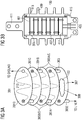
Fig. 3A shows astack 301 of electrically interconnected electronic circuit boards orwafers wafers Fig. 2A, Fig. 2B and Fig. 2C . Anadditional wafer 303 is provided which has thepower converter 103 and a voltage sense module (if required) located thereon. Asingle wafer interconnector further wafer interconnector 305E connects the additional wafer to the line connection of the HV network. Therefore, the PTH of the additional wafer connects the line connection of the HV network to the voltage sense module (if required) and thepower conversion system 101. The output of the power conversion system 101 (via the power converter 103) to the load electronics is provided by way of a furtherelectrical connection 307. The output of the voltage sense module to the load electronics is provided by way of a second furtherelectrical connection 309. - The
upper wafer 201D of the stack of wafers is connected to the ground connection of the HV network. - Therefore, the electrical
power conversion system 101 as described herein has surface mountedresistive components 215 and surface mountedcapacitive components 217 that are mounted on a plurality of electronic circuit boards forming a plurality of RC networks. There is one RC network on each electronic circuit board. The electronic circuit boards are stacked and electrically interconnected forming a stacked RC network. Further, the power converter may be mounted on a further electronic circuit board, where the further electronic circuit board forms part of the plurality of electronic circuit boards that are stacked.
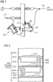
The stack of wafers may be assembled into an electrically insulated tube that has electrical terminals at opposing ends. The electrically insulated tube has suitable insulation properties for the desired electrical application. One such example of an electrically insulated tube could be the type of tube used to house an outdoor surge arrestor. -
Fig. 3B shows a cross-sectional view of anRC network stack 401 in ahousing 403.Fig. 3B shows how the stack may be assembled within a "surge arrestor" housing. At the bottom of the housing areconnections 405 to taking the low voltage power supply and the voltage measurement signal to a product from Siemens called a Fusesaver. - Fusesaver is a new class of intelligent, compact and low cost single phase circuit breaker that minimizes lost customer minutes by protecting lateral line (spur line or T-off) fuses from blowing on transient faults. With on-board microprocessor control and wireless connectivity, Fusesaver has configurable protection, multi-phase operation functions, on-board event history and can be integrated into a SCADA system for remote control.
- The Siemens Fusesaver product which can be powered from the line current obtained from HV networks. However, it would be advantageous if the Fusesaver was powered from line voltage. It will be understood that, although the principles described herein relate to the Fusesaver product, the principles may be applicable generally to other types of products and applications.
- The
wafer stack 401 with wafers interconnected viainterconnectors 305 is located within a cylindricalinsulated housing tube 407. Asilicone overmoulding 409 is fabricated and positioned so that it is located around the outer surface of thehousing tube 407. - A first
conductive end cap 411 is positioned at a first end of thehousing tube 407 and connects theupper wafer 413 of the wafer stack to the ground line of the HV network. That is, the firstconductive end cap 411 provides an electrical connection between one end of the RC network located on theupper wafer 413 and the ground line. - A second
conductive end cap 415 is positioned at a second end of thehousing tube 407 and connects thelower wafer 417 of the wafer stack to the Fusesaver body. That is, the secondconductive end cap 415 provides an electrical connection between the power converter (with or without the voltage sense module) located on thelower wafer 417 and the Fusesaver body, where the Fusesaver body is in direct connection with the line connection of the HV network (seeFig. 4 ). -
Fig. 4 shows a view of the device described above with reference toFig. 3B connected to the body of a Fusesaver device. -
Fig. 4 shows how the electrical power conversion system constructed as above in the form of a stacked RC network in an insulated tube could be mounted onto aSiemens Fusesaver product 421, which is installed on anelectrical spur line 423 with afuse 425. The upper end of the electrical power conversion system (i.e. the RC network) is connected to ground 427 of the HV network. The lower end of the electrical power conversion system (i.e. the power converter) is connected to theFusesaver body 429 which is at line potential as it is connected to themain line source 421 of the HV network. The power supply output from the switched mode DC-DC power converter and the voltage measurement signal from the voltage sense module are not visible as they are connected internally within the Fusesaver product. - It will be understood that many other suitable configurations are possible besides that shown in
Fig. 4 . - It will be understood that the power conversion system may include one or
more RC networks 1050 and one ormore power converters 103, where thepower converters 103 andRC networks 1050 are connected in series across a line potential of the HV power supply. - According to a first example, a
power conversion system 101 may have asingle RC network 1050 and asingle power converter 103 connected in series, where theRC network 1050 is connected to the ground connection of a single phase HV network and thepower converter 103 is connected to the line connection of the single phase HV network. - Alternatively, the HV network may be a polyphase network.
- Alternatively, the HV network may be a polyphase network where the
RC network 1050 is connected to the ground connection and phase converter is connected to one of the line connections. - According to a second example, a power conversion system may have a single RC network and a single power converter connected in series, where the RC network is connected to the line connection of a single phase HV network and the power converter is connected to the ground connection of the single phase HV network.
- Alternatively, the HV network may be a polyphase network where the RC network is connected to one of the line connections and phase converter is connected to the ground connection.
- According to a third example, a power conversion system may have a single RC network and a single power converter connected in series, where the RC network is connected to a first line connection of a polyphase HV network and the power converter is connected to a second line connection of the polyphase HV network. That is, the RC network and phase converter are connected between two different phases of the HV network.
- According to a fourth example, a power conversion system may have a single RC network and a first and second power converter connected in series either side of the RC network, where the first power converter is connected to a first line connection of a polyphase HV network and the second power converter is connected to a second line connection of the polyphase HV network. That is, the RC network and two phase converters are connected between two different phases of the HV network.
- According to a fifth example, a power conversion system may have a single RC network and a first and second power converter connected in series either side of the RC network, where the first power converter is connected to a line connection of a single phase HV network and the second power converter is connected to a ground connection of the polyphase HV network.
-
Fig. 5 shows a stack of electrically interconnected electronic circuit boards, wafers, within insulatingcups cups wafers RC chain networks springs cups channel springs cups -
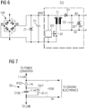
Fig. 6 shows a schematic diagram of apower converter 103 including a switching DC-DC power converter 111 (switch mode power supply). Acontrol circuit 601 provides high frequency switching control of switching transistor Q1, which feeds power to the primary winding of a forward step-down transformer T1. The output of the secondary winding of T1 is rectified by diode D1 and feeds a reservoir capacitor C2. The Zener diode Z2 limits the output voltage to 6V. The output power generated by the switch mode power supply (SMPS) is provided to the load electronic system. - As can be seen the SMPS is operated with a high voltage in the order of 300V on the primary side and in conjunction with the RC chain solution as described herein. The SMPS converts from approximately 300V to the output voltage required by the load electronics.
-
Fig. 7 shows a schematic diagram of avoltage sense module 701. The current flowing through theRC chain network 1050 is essentially proportional to the phase-ground voltage of the HV network. This can be converted electronically into a suitable sense signal for the Fusesaver electronics by the line voltage sense module shown inFig. 7 . This therefore provides a system for monitoring the status of the phase-ground voltage. - In this circuit the RC chain current is converted to voltage by a resistor R100 in series with a capacitor C100. By selecting correct values for R100 and C100, the phase shift introduced by the RC chain network is corrected so that the voltage output of the voltage sense module is in phase with the line voltage signal of the HV network.
- To avoid trapped charges in the capacitive components to build up, resistor R111 1050' allows a trapped charge in the capacitive component c100 to drop off the capacitive component C100.
- It will be understood that there are many other possible implementations to correct for the phase shift caused by the RC chain network including, for example, signal processing to derive the corrected signal.
- Therefore, the electrical power conversion system has a voltage sense module that is adapted to measure a current flowing through the RC network and convert that current to a sensor voltage value for use by sensing electronics. Further, the voltage sense module is arranged to correct the phase shift caused by the RC network.
- In order to overcome the inherent inaccuracy of the described method of voltage sensor measurement provided by the voltage sense module due to the power converter subtracting 300V from line voltage driving the current in the RC chain, a voltage loss correction module may be incorporated into the downstream electronics which is processing the signal from the voltage sense module to correct the sensor voltage value based on voltage losses caused by the power conversion system.
- Without the voltage loss correction module, if the peak line voltage is below 300V no current will flow in the line voltage sense resistor. Also, at line voltages above 300V peak, the 300V would be subtracted from the instantaneous value measured by the voltage sense module.
- To correct for the inaccuracy at voltages above the 300V threshold due to the power conversion system, 300V can be digitally added by the voltage loss correction module to each of the samples. For 1 ms sampling of a 6.3 kV signal this method reduces the measurement error from 4.5% to 0.02%. It will be understood that other methods of error correction are envisaged.
- Control of electrical stress is critical to the long term reliability of insulating products. The herein described systems enable electrical stress to be predicted and well controlled as well as being relatively independent of manufacturing variations.
- Electrical stresses on the resistive and capacitive components may be calculated under the various PF conditions to be withstood (such as phase/ground voltage, PF test) using commonplace electronic design practices. These values may be used to determine the number of components required to meet the component manufacturers rating, tolerance aspects etc. Transverse electrical stress between elements of the RC network chain is controlled by the component layout (i.e. the configuration of the RC network) on the wafer PCB. The design requirement is to meet the appropriate surface electrical stress for the product environment and the PCB material. The determination of the appropriate stress and configuration results in the chain angle as shown in
Fig. 2A . - Wafer axial stress is dependent on the voltage developed across each wafer and the wafer spacing. Finite element analysis can be used to calculate stresses and stress can be further controlled by use of a conformal coating (to reduce triple point stress), and interposing insulating elements. In this example, stacking cups may be used to assemble the wafer stack and to provide additional insulation as shown in
Fig. 5 . - Various advantages are provided for certain features as described herein as follows:
Use of anRC network 1050 to provide a power source from a power line of an HV network: - This provides an advantage that current is limited at both PF and impulse conditions with the advantage of low power dissipation at normal voltages.
- Further, power can be supplied to either a grounded device, to a device floating at line potential or to both.
- Use of SMPS to convert current to useable power with high frequency switching:
This provides an advantage in that the cost and size of making a PF transformer is negated. Using a SMPS enables high efficiency, low cost, and small size conversion of the power from the RC network. - Use of multiple SMT components on circuit boards to make the RC network:
This provides various advantages including, for example, the minimisation of costs, control of electrical stresses and the provision of graceful degradation for component failure. - Use of stacked wafer construction:
This provides various advantages including, for example, controlling electrical stresses and allowing various rated voltages to be achieved using multiple sets of the same basic component parts. - Use of stacking cups:
This provides various advantages including, for example, controlling electrical stresses and minimising costs. - Addition of voltage sensing network to provide voltage sensing from the current provided by the RC chain:
- This provides various advantages including, for example, enabling line voltage measurement.
- Digital correction of distortion of voltage sensing due to power take off:
This provides various advantages including, for example, improving accuracy from RC chain. - Although the example shown in
Fig.1 shows theRC network 1050 connected to the ground connection of the HV network, and thepower converter 103 connected to the line connection of the HV network (via the optional voltage sense module), as mentioned above it will be understood that, as an alternative, theRC network 1050 may be connected to the line connection of the HV network and thepower converter 103 may be connected to the ground connection of the HV network. - As a further alternative, as mentioned above, the
RC network 1050 may be connected to a first line connection (i.e. a first phase of the three-phase HV network) and thepower converter 103 may be connected to a second line connection (i.e. a second phase of the three-phase HV network. - It will be understood that, according to further alternatives, the power converter of the
power conversion system 101 may be located at - i) the grounded end of the HV network to supply a grounded electronic system,
- ii) at the line end of the HV network to supply an electronic system floating at line potential, or
- iii) where there are multiple power converters, at both ends.
- It will be understood that, according to a further alternative, the power converter module may be an AC-DC power converter module and that the
power converter 103 does not require therectifier 109, capacitor C10 and the Zener diode Z10. - As a further alternative, it will be understood that the power converter may be placed on a wafer in order to create a self-contained electrical
power conversion system 101 which may then be connected directly to the HV network. - Further, the voltage sense module may be located on the power converter wafer to condition the current flowing in the RC network chain into a signal for the load electronics to measure the line-ground voltage, as discussed in more detail herein.
- According to the above described example, there are an equal number of resistors and capacitors in the series RC chain. However, it will be understood that, as an alternative, there may be more resistors than capacitors, or more capacitors than resistors.
- It will be understood that, as an alternative, there may be more than one
series RC network 1050. For example, multiple series RC networks may be connected between HV electrical power supply and the power converter either in series or in parallel, e.g. to provide a level of redundancy. - It will be understood that, as an alternative, there are many integrated circuits that are available to perform the function of the SMPS.
- Further, it would be understood that there are many possible circuit topologies such as, for example, forward or fly back, isolated or non-isolated etc.
Claims (14)
- An electrical power conversion system (101) for converting a high voltage (HV) from a HV electrical power supply to a low voltage, wherein the electrical power conversion system (101) comprises:at least one power converter (103), andat least one RC network (1050) comprising a plurality of resistive components (1051, 1054, 1057) and a plurality of capacitive components (1052, 1055, 1058) electrically connected in series, wherein the at least one RC network (1050) is in series connection with the at least one power converter (103), and the at least one RC network (1050) and at least one power converter (103) are arranged to be connected across a line potential of the HV electrical power supply,CHARACTERISED IN THAT, high resistance drop off elements (1053, 1056, 1059) are connected in parallel to the capacitive components (1052, 1055, 1058) of the RC network (1050).
- The electrical power conversion system (101) of claim 1,
CHARACTERISED IN THAT,
the high resistance drop off elements (1053, 1056, 1059) are high value resistors (R11, R22, R33). - The electrical power conversion system (101) of claim 2,
CHARACTERISED IN THAT,
the high value resistors (R11, R22, R33are designed to allow a trapped charge in the capacitive components (1052, 1055, 1058) to drop off the capacitive components (1052, 1055, 1058). - The electrical power conversion system (101) of claim 1,
CHARACTERISED IN THAT,
the high resistance drop off elements (1053, 1056, 1059) are realized by a conductive coating on a printed circuit board holding at least the capacitive components (1052, 1055, 1058). - The electrical power conversion system (101) of any of the preceding claims,
CHARACTERISED IN THAT,
the power converter (103) comprises a switch mode power supply. - The electrical power conversion system (101) of any of the preceding claims,
CHARACTERISED IN THAT,
the resistive components (1051, 1054, 1057) are surface mounted resistive components (1051, 1054, 1057) and the capacitive components (1052, 1055, 1058) are surface mounted capacitive components (1052, 1055, 1058), and
the surface mounted resistive components (1051, 1054, 1057) and the surface mounted capacitive components (1052, 1055, 1058) are mounted on one or more electronic circuit boards forming the RC network (1050) on the one or more electronic circuit boards (201). - The electrical power conversion system (101) of claim 6,
CHARACTERISED IN THAT,
the surface mounted resistive components (1051, 1054, 1057) and the surface mounted capacitive components (1052, 1055, 1058) are mounted on a plurality of electronic circuit boards (201A, 201B, 201C, 201D) forming a plurality of RC networks (201A, 201B, 201C, 201D) with one RC network on each electronic circuit board, and
the plurality of electronic circuit boards (201A, 201B, 201C, 201D) are stacked and electrically interconnected forming a stacked RC network. - The electrical power conversion system (101) of claim 7,
CHARACTERISED IN THAT,
the power converter (103) is mounted on a further electronic circuit board (303), and the further electronic circuit board (303) forms part of the plurality of electronic circuit boards that are stacked. - The electrical power conversion system (101) of claim 6,
CHARACTERISED IN THAT,
the power conversion system (101) further comprises one or more insulated circuit board receptacles arranged to support the one or more electronic circuit boards (201A, 201B, 201C). - The electrical power conversion system (101) of claim 9,
CHARACTERISED IN THAT,
the power conversion system (101) further comprises a plurality of the insulated circuit board receptacles, each arranged to support one of a plurality of the electrically interconnected electronic circuit boards (201A, 201B, 201C) in a stacked configuration. - The electrical power conversion system (101) of any of the preceding claims,
CHARACTERISED IN THAT,
the power conversion system (101) further comprises a voltage sense module adapted to measure a current flowing through the RC network (1050) and convert the current to a sensor voltage value. - The electrical power conversion system (101) of claim 11,
CHARACTERISED IN THAT,
the power conversion system (101) further comprises a voltage loss correction module, wherein the voltage loss correction module is adapted to correct the sensor voltage value based on voltage losses caused by the power converter. - The electrical power conversion system (101) of any of the preceding claims,
CHARACTERISED IN THAT,
the at least one RC network (1050) and at least one power converter (103) are arranged to be connected between a line connection of the HV electrical power supply and a ground connection of the HV electrical supply. - The electrical power conversion system (101) of any of the preceding claims,
CHARACTERISED IN THAT,
the at least one RC network (1050) and at least one power converter (103) are arranged to be connected between a first line connection of the HV electrical power supply and a second line connection of the HV electrical supply.
Priority Applications (5)
| Application Number | Priority Date | Filing Date | Title |
|---|---|---|---|
| EP18196756.3A EP3629465A1 (en) | 2018-09-26 | 2018-09-26 | Electrical power conversion system |
| AU2019226249A AU2019226249B2 (en) | 2018-09-26 | 2019-09-06 | Electrical power conversion system |
| CA3055064A CA3055064C (en) | 2018-09-26 | 2019-09-11 | Electrical power conversion system |
| BR102019019929A BR102019019929A2 (en) | 2018-09-26 | 2019-09-24 | electric power conversion system |
| US16/583,547 US11031874B2 (en) | 2018-09-26 | 2019-09-26 | Electrical power conversion system |
Applications Claiming Priority (1)
| Application Number | Priority Date | Filing Date | Title |
|---|---|---|---|
| EP18196756.3A EP3629465A1 (en) | 2018-09-26 | 2018-09-26 | Electrical power conversion system |
Publications (1)
| Publication Number | Publication Date |
|---|---|
| EP3629465A1 true EP3629465A1 (en) | 2020-04-01 |
Family
ID=63685642
Family Applications (1)
| Application Number | Title | Priority Date | Filing Date |
|---|---|---|---|
| EP18196756.3A Pending EP3629465A1 (en) | 2018-09-26 | 2018-09-26 | Electrical power conversion system |
Country Status (5)
| Country | Link |
|---|---|
| US (1) | US11031874B2 (en) |
| EP (1) | EP3629465A1 (en) |
| AU (1) | AU2019226249B2 (en) |
| BR (1) | BR102019019929A2 (en) |
| CA (1) | CA3055064C (en) |
Citations (3)
| Publication number | Priority date | Publication date | Assignee | Title |
|---|---|---|---|---|
| US4408269A (en) * | 1982-06-18 | 1983-10-04 | Zenith Radio Corporation | Balanced power supply with polarized capacitors |
| DE3714945A1 (en) * | 1986-05-09 | 1987-11-12 | Koch & Sterzel Kg | Frequency-independent capacitive/resistive voltage divider for measuring high voltages in medium- and high-frequency X-ray generators |
| US7304872B1 (en) | 2004-09-24 | 2007-12-04 | Field Metrics, Inc. | Power supply |
Family Cites Families (25)
| Publication number | Priority date | Publication date | Assignee | Title |
|---|---|---|---|---|
| US4117527A (en) * | 1977-03-25 | 1978-09-26 | General Electric Company | Solid state valve thermal protection for hvdc power converters |
| US4131939A (en) * | 1977-03-30 | 1978-12-26 | Day Ralph D | Constant current power supply |
| NL7809226A (en) * | 1978-09-11 | 1980-03-13 | Philips Nv | SWITCHED VOLTAGE CONVERTER. |
| FR2706699B1 (en) | 1993-06-10 | 1995-09-15 | Gec Alsthom T & D Sa | Device for supplying a voltage to an electronic circuit, in particular to an electronic circuit associated with an intensity sensor placed on an electric line. |
| DE19509329C1 (en) * | 1995-03-15 | 1996-11-28 | Siemens Ag | Circuit arrangement |
| US5936357A (en) * | 1998-07-24 | 1999-08-10 | Energy Savings, Inc. | Electronic ballast that manages switching frequencies for extrinsic purposes |
| US6061259A (en) * | 1999-08-30 | 2000-05-09 | Demichele; Glenn | Protected transformerless AC to DC power converter |
| US6188588B1 (en) * | 1999-10-07 | 2001-02-13 | International Business Machine Corporation | Switching controller and method for operating a flyback converter in a critically continuous conduction mode |
| US6633154B1 (en) * | 2000-01-04 | 2003-10-14 | William B. Duff, Jr. | Method and circuit for using polarized device in AC applications |
| TW522623B (en) * | 2001-06-13 | 2003-03-01 | Delta Electronics Inc | Inrush current protection circuit |
| US6714429B2 (en) * | 2001-08-15 | 2004-03-30 | Astec International Limited | Active inrush current control for AC to DC converters |
| US7663351B2 (en) * | 2006-08-30 | 2010-02-16 | Texas Instruments Incorporated | Synchronization circuitry for multiple power converters coupled at a common node |
| US10492265B1 (en) * | 2012-06-15 | 2019-11-26 | Aleddra Inc. | Solid-state lighting with a control gear cascaded by a luminaire |
| EP2750257B1 (en) * | 2012-09-17 | 2016-05-11 | GE Energy Power Conversion Technology Ltd | Circuit breakers |
| US9143030B2 (en) * | 2012-10-09 | 2015-09-22 | Teledyne Reynolds, Inc. | Passive power factor correction incorporating AC/DC conversion |
| US20140177304A1 (en) * | 2012-12-24 | 2014-06-26 | Laurence P. Sadwick | Constant Current Source |
| US9671799B2 (en) * | 2013-02-04 | 2017-06-06 | Infineon Technologies Austria Ag | System and method for a power supply controller |
| US10084376B2 (en) * | 2013-06-13 | 2018-09-25 | Silicon Laboratories Inc. | Circuit with multiple output power converter |
| AU2014206162B2 (en) * | 2014-07-24 | 2019-03-14 | Siemens Aktiengesellschaft | Electrical power conversion system |
| WO2016032981A1 (en) * | 2014-08-25 | 2016-03-03 | NuVolta Technologies | Wireless power transfer system and method |
| US9338853B2 (en) * | 2014-09-17 | 2016-05-10 | Greco Tech Industries Inc. | LED tube driver circuitry for ballast and non-ballast fluorescent tube replacement |
| WO2016141490A1 (en) * | 2015-03-11 | 2016-09-15 | Telcodium Inc. | Power supply connecting board with multiple programmable output voltage levels |
| EP3113578B1 (en) * | 2015-06-30 | 2018-08-08 | Nxp B.V. | A filter circuit |
| US10620275B2 (en) * | 2016-08-25 | 2020-04-14 | GM Global Technology Operations LLC | State estimation of an energy system |
| US10848053B2 (en) * | 2018-07-13 | 2020-11-24 | Kohler Co. | Robust inverter topology |
-
2018
- 2018-09-26 EP EP18196756.3A patent/EP3629465A1/en active Pending
-
2019
- 2019-09-06 AU AU2019226249A patent/AU2019226249B2/en active Active
- 2019-09-11 CA CA3055064A patent/CA3055064C/en active Active
- 2019-09-24 BR BR102019019929A patent/BR102019019929A2/en unknown
- 2019-09-26 US US16/583,547 patent/US11031874B2/en active Active
Patent Citations (3)
| Publication number | Priority date | Publication date | Assignee | Title |
|---|---|---|---|---|
| US4408269A (en) * | 1982-06-18 | 1983-10-04 | Zenith Radio Corporation | Balanced power supply with polarized capacitors |
| DE3714945A1 (en) * | 1986-05-09 | 1987-11-12 | Koch & Sterzel Kg | Frequency-independent capacitive/resistive voltage divider for measuring high voltages in medium- and high-frequency X-ray generators |
| US7304872B1 (en) | 2004-09-24 | 2007-12-04 | Field Metrics, Inc. | Power supply |
Also Published As
| Publication number | Publication date |
|---|---|
| US20200099308A1 (en) | 2020-03-26 |
| US11031874B2 (en) | 2021-06-08 |
| BR102019019929A2 (en) | 2020-04-07 |
| CA3055064A1 (en) | 2020-03-26 |
| AU2019226249B2 (en) | 2021-07-01 |
| CA3055064C (en) | 2022-03-22 |
| AU2019226249A1 (en) | 2020-04-09 |
Similar Documents
| Publication | Publication Date | Title |
|---|---|---|
| EP3152826B1 (en) | Electrical power conversion system | |
| US8964433B2 (en) | Insulator integrated power supply | |
| EP2156449B1 (en) | High frequency transformer for high voltage applications | |
| US7990242B2 (en) | Transient voltage and harmonic currents quashing (THQ) transformers, transformer winding topology, and method of making the same | |
| US11378594B2 (en) | Capacitive voltage sensor with hidden sensing electrode | |
| AU2019226249B2 (en) | Electrical power conversion system | |
| EP2747098B1 (en) | Transformer arrangement for mitigating transient voltage oscillations | |
| EP3767653B1 (en) | Transformer assembly with medium frequency transformers | |
| RU2733535C1 (en) | Inverter device | |
| EP3125260B1 (en) | Transformer for a modular, power electronic converter | |
| JP6527952B2 (en) | Circuit arrangement with transformer with center tap and measurement of output voltage | |
| Ellis et al. | Innovative protection schemes for H configuration fuseless grounded shunt capacitor banks | |
| CN109417849B (en) | Current separation device | |
| JP6807855B2 (en) | Resonant converter with transformer with center tap | |
| Watson | A Novel Voltage Based Approach to Self Powering the Next Generation of Smart, Compact and Communicable Auto-Reclosers for Distribution Networks | |
| US11211789B2 (en) | Capacitive power supply circuit | |
| US20220413018A1 (en) | Voltage sampler and solid-state transformer | |
| JP4361923B2 (en) | GPT addition type ground voltage suppression device | |
| KR20240004647A (en) | Power flow control module for use in low-voltage distribution networks | |
| CN104752031A (en) | Pulse transformer, switching power supply with same and residual current device |
Legal Events
| Date | Code | Title | Description |
|---|---|---|---|
| PUAI | Public reference made under article 153(3) epc to a published international application that has entered the european phase |
Free format text: ORIGINAL CODE: 0009012 |
|
| STAA | Information on the status of an ep patent application or granted ep patent |
Free format text: STATUS: THE APPLICATION HAS BEEN PUBLISHED |
|
| AK | Designated contracting states |
Kind code of ref document: A1 Designated state(s): AL AT BE BG CH CY CZ DE DK EE ES FI FR GB GR HR HU IE IS IT LI LT LU LV MC MK MT NL NO PL PT RO RS SE SI SK SM TR |
|
| AX | Request for extension of the european patent |
Extension state: BA ME |
|
| STAA | Information on the status of an ep patent application or granted ep patent |
Free format text: STATUS: REQUEST FOR EXAMINATION WAS MADE |
|
| 17P | Request for examination filed |
Effective date: 20200929 |
|
| RBV | Designated contracting states (corrected) |
Designated state(s): AL AT BE BG CH CY CZ DE DK EE ES FI FR GB GR HR HU IE IS IT LI LT LU LV MC MK MT NL NO PL PT RO RS SE SI SK SM TR |
|
| STAA | Information on the status of an ep patent application or granted ep patent |
Free format text: STATUS: EXAMINATION IS IN PROGRESS |
|
| STAA | Information on the status of an ep patent application or granted ep patent |
Free format text: STATUS: EXAMINATION IS IN PROGRESS |
|
| 17Q | First examination report despatched |
Effective date: 20210811 |
|
| APBK | Appeal reference recorded |
Free format text: ORIGINAL CODE: EPIDOSNREFNE |
|
| APBN | Date of receipt of notice of appeal recorded |
Free format text: ORIGINAL CODE: EPIDOSNNOA2E |
|
| APBR | Date of receipt of statement of grounds of appeal recorded |
Free format text: ORIGINAL CODE: EPIDOSNNOA3E |
|
| APAF | Appeal reference modified |
Free format text: ORIGINAL CODE: EPIDOSCREFNE |