EP3609022A1 - Light-transmissive antenna, window affixing type communication module, and periphery monitoring unit - Google Patents
Light-transmissive antenna, window affixing type communication module, and periphery monitoring unit Download PDFInfo
- Publication number
- EP3609022A1 EP3609022A1 EP18781108.8A EP18781108A EP3609022A1 EP 3609022 A1 EP3609022 A1 EP 3609022A1 EP 18781108 A EP18781108 A EP 18781108A EP 3609022 A1 EP3609022 A1 EP 3609022A1
- Authority
- EP
- European Patent Office
- Prior art keywords
- antenna
- electrically conductive
- pattern
- transparent base
- transparent
- Prior art date
- Legal status (The legal status is an assumption and is not a legal conclusion. Google has not performed a legal analysis and makes no representation as to the accuracy of the status listed.)
- Granted
Links
- 238000012544 monitoring process Methods 0.000 title claims description 25
- 238000004891 communication Methods 0.000 title claims description 24
- 238000002834 transmittance Methods 0.000 claims abstract description 41
- 239000011810 insulating material Substances 0.000 claims abstract description 6
- 239000005357 flat glass Substances 0.000 claims description 9
- 238000003384 imaging method Methods 0.000 claims description 8
- 238000000926 separation method Methods 0.000 claims description 8
- 238000012545 processing Methods 0.000 claims description 5
- 239000010408 film Substances 0.000 description 44
- 238000012986 modification Methods 0.000 description 37
- 230000004048 modification Effects 0.000 description 37
- 238000010586 diagram Methods 0.000 description 25
- 239000000463 material Substances 0.000 description 23
- 239000000203 mixture Substances 0.000 description 19
- 239000011521 glass Substances 0.000 description 11
- 230000000052 comparative effect Effects 0.000 description 10
- 239000011347 resin Substances 0.000 description 10
- 229920005989 resin Polymers 0.000 description 10
- 230000005540 biological transmission Effects 0.000 description 9
- 238000004088 simulation Methods 0.000 description 9
- 230000009467 reduction Effects 0.000 description 8
- 239000004020 conductor Substances 0.000 description 6
- RYGMFSIKBFXOCR-UHFFFAOYSA-N Copper Chemical compound [Cu] RYGMFSIKBFXOCR-UHFFFAOYSA-N 0.000 description 5
- 230000015572 biosynthetic process Effects 0.000 description 5
- 230000000694 effects Effects 0.000 description 5
- XLOMVQKBTHCTTD-UHFFFAOYSA-N Zinc monoxide Chemical compound [Zn]=O XLOMVQKBTHCTTD-UHFFFAOYSA-N 0.000 description 4
- 239000011889 copper foil Substances 0.000 description 4
- 238000009826 distribution Methods 0.000 description 3
- 230000005684 electric field Effects 0.000 description 3
- 230000001965 increasing effect Effects 0.000 description 3
- 239000010409 thin film Substances 0.000 description 3
- 239000012780 transparent material Substances 0.000 description 3
- XEEYBQQBJWHFJM-UHFFFAOYSA-N Iron Chemical compound [Fe] XEEYBQQBJWHFJM-UHFFFAOYSA-N 0.000 description 2
- PXHVJJICTQNCMI-UHFFFAOYSA-N Nickel Chemical compound [Ni] PXHVJJICTQNCMI-UHFFFAOYSA-N 0.000 description 2
- BQCADISMDOOEFD-UHFFFAOYSA-N Silver Chemical compound [Ag] BQCADISMDOOEFD-UHFFFAOYSA-N 0.000 description 2
- 229910052782 aluminium Inorganic materials 0.000 description 2
- XAGFODPZIPBFFR-UHFFFAOYSA-N aluminium Chemical compound [Al] XAGFODPZIPBFFR-UHFFFAOYSA-N 0.000 description 2
- 230000007423 decrease Effects 0.000 description 2
- 239000003989 dielectric material Substances 0.000 description 2
- 210000000887 face Anatomy 0.000 description 2
- 238000004519 manufacturing process Methods 0.000 description 2
- 238000005192 partition Methods 0.000 description 2
- BASFCYQUMIYNBI-UHFFFAOYSA-N platinum Chemical compound [Pt] BASFCYQUMIYNBI-UHFFFAOYSA-N 0.000 description 2
- 238000004904 shortening Methods 0.000 description 2
- 239000011787 zinc oxide Substances 0.000 description 2
- 239000004925 Acrylic resin Substances 0.000 description 1
- 229920000178 Acrylic resin Polymers 0.000 description 1
- 229920002284 Cellulose triacetate Polymers 0.000 description 1
- 229920000089 Cyclic olefin copolymer Polymers 0.000 description 1
- GYHNNYVSQQEPJS-UHFFFAOYSA-N Gallium Chemical compound [Ga] GYHNNYVSQQEPJS-UHFFFAOYSA-N 0.000 description 1
- 239000002042 Silver nanowire Substances 0.000 description 1
- ATJFFYVFTNAWJD-UHFFFAOYSA-N Tin Chemical compound [Sn] ATJFFYVFTNAWJD-UHFFFAOYSA-N 0.000 description 1
- NNLVGZFZQQXQNW-ADJNRHBOSA-N [(2r,3r,4s,5r,6s)-4,5-diacetyloxy-3-[(2s,3r,4s,5r,6r)-3,4,5-triacetyloxy-6-(acetyloxymethyl)oxan-2-yl]oxy-6-[(2r,3r,4s,5r,6s)-4,5,6-triacetyloxy-2-(acetyloxymethyl)oxan-3-yl]oxyoxan-2-yl]methyl acetate Chemical compound O([C@@H]1O[C@@H]([C@H]([C@H](OC(C)=O)[C@H]1OC(C)=O)O[C@H]1[C@@H]([C@@H](OC(C)=O)[C@H](OC(C)=O)[C@@H](COC(C)=O)O1)OC(C)=O)COC(=O)C)[C@@H]1[C@@H](COC(C)=O)O[C@@H](OC(C)=O)[C@H](OC(C)=O)[C@H]1OC(C)=O NNLVGZFZQQXQNW-ADJNRHBOSA-N 0.000 description 1
- 230000009471 action Effects 0.000 description 1
- 239000000956 alloy Substances 0.000 description 1
- 239000000919 ceramic Substances 0.000 description 1
- 239000000470 constituent Substances 0.000 description 1
- 229910052802 copper Inorganic materials 0.000 description 1
- 239000010949 copper Substances 0.000 description 1
- 230000008878 coupling Effects 0.000 description 1
- 238000010168 coupling process Methods 0.000 description 1
- 238000005859 coupling reaction Methods 0.000 description 1
- 238000013461 design Methods 0.000 description 1
- 229910052733 gallium Inorganic materials 0.000 description 1
- PCHJSUWPFVWCPO-UHFFFAOYSA-N gold Chemical compound [Au] PCHJSUWPFVWCPO-UHFFFAOYSA-N 0.000 description 1
- 229910052737 gold Inorganic materials 0.000 description 1
- 239000010931 gold Substances 0.000 description 1
- 229910003437 indium oxide Inorganic materials 0.000 description 1
- PJXISJQVUVHSOJ-UHFFFAOYSA-N indium(iii) oxide Chemical compound [O-2].[O-2].[O-2].[In+3].[In+3] PJXISJQVUVHSOJ-UHFFFAOYSA-N 0.000 description 1
- AMGQUBHHOARCQH-UHFFFAOYSA-N indium;oxotin Chemical compound [In].[Sn]=O AMGQUBHHOARCQH-UHFFFAOYSA-N 0.000 description 1
- 229910052742 iron Inorganic materials 0.000 description 1
- 238000005259 measurement Methods 0.000 description 1
- 229910052751 metal Inorganic materials 0.000 description 1
- 239000002184 metal Substances 0.000 description 1
- 150000002739 metals Chemical class 0.000 description 1
- 238000000034 method Methods 0.000 description 1
- 229910052759 nickel Inorganic materials 0.000 description 1
- 229910052697 platinum Inorganic materials 0.000 description 1
- 229920003229 poly(methyl methacrylate) Polymers 0.000 description 1
- 229920005668 polycarbonate resin Polymers 0.000 description 1
- 239000004431 polycarbonate resin Substances 0.000 description 1
- 229920001225 polyester resin Polymers 0.000 description 1
- 239000004645 polyester resin Substances 0.000 description 1
- -1 polyethylene terephthalate Polymers 0.000 description 1
- 229920000139 polyethylene terephthalate Polymers 0.000 description 1
- 239000005020 polyethylene terephthalate Substances 0.000 description 1
- 229920001721 polyimide Polymers 0.000 description 1
- 239000009719 polyimide resin Substances 0.000 description 1
- 239000004926 polymethyl methacrylate Substances 0.000 description 1
- 229920005672 polyolefin resin Polymers 0.000 description 1
- 230000005855 radiation Effects 0.000 description 1
- 229910052709 silver Inorganic materials 0.000 description 1
- 239000004332 silver Substances 0.000 description 1
- 238000009751 slip forming Methods 0.000 description 1
- 238000012360 testing method Methods 0.000 description 1
- 229910052718 tin Inorganic materials 0.000 description 1
- 239000011135 tin Substances 0.000 description 1
Images


Classifications
-
- H—ELECTRICITY
- H01—ELECTRIC ELEMENTS
- H01Q—ANTENNAS, i.e. RADIO AERIALS
- H01Q13/00—Waveguide horns or mouths; Slot antennas; Leaky-waveguide antennas; Equivalent structures causing radiation along the transmission path of a guided wave
- H01Q13/08—Radiating ends of two-conductor microwave transmission lines, e.g. of coaxial lines, of microstrip lines
-
- B—PERFORMING OPERATIONS; TRANSPORTING
- B60—VEHICLES IN GENERAL
- B60R—VEHICLES, VEHICLE FITTINGS, OR VEHICLE PARTS, NOT OTHERWISE PROVIDED FOR
- B60R1/00—Optical viewing arrangements; Real-time viewing arrangements for drivers or passengers using optical image capturing systems, e.g. cameras or video systems specially adapted for use in or on vehicles
- B60R1/12—Mirror assemblies combined with other articles, e.g. clocks
-
- H—ELECTRICITY
- H01—ELECTRIC ELEMENTS
- H01B—CABLES; CONDUCTORS; INSULATORS; SELECTION OF MATERIALS FOR THEIR CONDUCTIVE, INSULATING OR DIELECTRIC PROPERTIES
- H01B5/00—Non-insulated conductors or conductive bodies characterised by their form
- H01B5/14—Non-insulated conductors or conductive bodies characterised by their form comprising conductive layers or films on insulating-supports
-
- H—ELECTRICITY
- H01—ELECTRIC ELEMENTS
- H01Q—ANTENNAS, i.e. RADIO AERIALS
- H01Q1/00—Details of, or arrangements associated with, antennas
- H01Q1/12—Supports; Mounting means
-
- H—ELECTRICITY
- H01—ELECTRIC ELEMENTS
- H01Q—ANTENNAS, i.e. RADIO AERIALS
- H01Q1/00—Details of, or arrangements associated with, antennas
- H01Q1/12—Supports; Mounting means
- H01Q1/1271—Supports; Mounting means for mounting on windscreens
-
- H—ELECTRICITY
- H01—ELECTRIC ELEMENTS
- H01Q—ANTENNAS, i.e. RADIO AERIALS
- H01Q1/00—Details of, or arrangements associated with, antennas
- H01Q1/12—Supports; Mounting means
- H01Q1/22—Supports; Mounting means by structural association with other equipment or articles
-
- H—ELECTRICITY
- H01—ELECTRIC ELEMENTS
- H01Q—ANTENNAS, i.e. RADIO AERIALS
- H01Q1/00—Details of, or arrangements associated with, antennas
- H01Q1/27—Adaptation for use in or on movable bodies
- H01Q1/32—Adaptation for use in or on road or rail vehicles
- H01Q1/3208—Adaptation for use in or on road or rail vehicles characterised by the application wherein the antenna is used
- H01Q1/3233—Adaptation for use in or on road or rail vehicles characterised by the application wherein the antenna is used particular used as part of a sensor or in a security system, e.g. for automotive radar, navigation systems
-
- H—ELECTRICITY
- H01—ELECTRIC ELEMENTS
- H01Q—ANTENNAS, i.e. RADIO AERIALS
- H01Q1/00—Details of, or arrangements associated with, antennas
- H01Q1/36—Structural form of radiating elements, e.g. cone, spiral, umbrella; Particular materials used therewith
- H01Q1/364—Structural form of radiating elements, e.g. cone, spiral, umbrella; Particular materials used therewith using a particular conducting material, e.g. superconductor
-
- H—ELECTRICITY
- H01—ELECTRIC ELEMENTS
- H01Q—ANTENNAS, i.e. RADIO AERIALS
- H01Q1/00—Details of, or arrangements associated with, antennas
- H01Q1/36—Structural form of radiating elements, e.g. cone, spiral, umbrella; Particular materials used therewith
- H01Q1/38—Structural form of radiating elements, e.g. cone, spiral, umbrella; Particular materials used therewith formed by a conductive layer on an insulating support
-
- H—ELECTRICITY
- H01—ELECTRIC ELEMENTS
- H01Q—ANTENNAS, i.e. RADIO AERIALS
- H01Q19/00—Combinations of primary active antenna elements and units with secondary devices, e.g. with quasi-optical devices, for giving the antenna a desired directional characteristic
- H01Q19/005—Patch antenna using one or more coplanar parasitic elements
-
- H—ELECTRICITY
- H01—ELECTRIC ELEMENTS
- H01Q—ANTENNAS, i.e. RADIO AERIALS
- H01Q21/00—Antenna arrays or systems
- H01Q21/29—Combinations of different interacting antenna units for giving a desired directional characteristic
- H01Q21/293—Combinations of different interacting antenna units for giving a desired directional characteristic one unit or more being an array of identical aerial elements
-
- H—ELECTRICITY
- H01—ELECTRIC ELEMENTS
- H01Q—ANTENNAS, i.e. RADIO AERIALS
- H01Q9/00—Electrically-short antennas having dimensions not more than twice the operating wavelength and consisting of conductive active radiating elements
- H01Q9/04—Resonant antennas
- H01Q9/0407—Substantially flat resonant element parallel to ground plane, e.g. patch antenna
- H01Q9/0428—Substantially flat resonant element parallel to ground plane, e.g. patch antenna radiating a circular polarised wave
-
- H—ELECTRICITY
- H01—ELECTRIC ELEMENTS
- H01Q—ANTENNAS, i.e. RADIO AERIALS
- H01Q9/00—Electrically-short antennas having dimensions not more than twice the operating wavelength and consisting of conductive active radiating elements
- H01Q9/04—Resonant antennas
- H01Q9/0407—Substantially flat resonant element parallel to ground plane, e.g. patch antenna
- H01Q9/045—Substantially flat resonant element parallel to ground plane, e.g. patch antenna with particular feeding means
-
- H—ELECTRICITY
- H01—ELECTRIC ELEMENTS
- H01Q—ANTENNAS, i.e. RADIO AERIALS
- H01Q9/00—Electrically-short antennas having dimensions not more than twice the operating wavelength and consisting of conductive active radiating elements
- H01Q9/04—Resonant antennas
- H01Q9/16—Resonant antennas with feed intermediate between the extremities of the antenna, e.g. centre-fed dipole
- H01Q9/28—Conical, cylindrical, cage, strip, gauze, or like elements having an extended radiating surface; Elements comprising two conical surfaces having collinear axes and adjacent apices and fed by two-conductor transmission lines
- H01Q9/285—Planar dipole
-
- B—PERFORMING OPERATIONS; TRANSPORTING
- B60—VEHICLES IN GENERAL
- B60R—VEHICLES, VEHICLE FITTINGS, OR VEHICLE PARTS, NOT OTHERWISE PROVIDED FOR
- B60R1/00—Optical viewing arrangements; Real-time viewing arrangements for drivers or passengers using optical image capturing systems, e.g. cameras or video systems specially adapted for use in or on vehicles
- B60R1/12—Mirror assemblies combined with other articles, e.g. clocks
- B60R2001/1261—Mirror assemblies combined with other articles, e.g. clocks with antennae
-
- H—ELECTRICITY
- H01—ELECTRIC ELEMENTS
- H01Q—ANTENNAS, i.e. RADIO AERIALS
- H01Q21/00—Antenna arrays or systems
- H01Q21/06—Arrays of individually energised antenna units similarly polarised and spaced apart
- H01Q21/08—Arrays of individually energised antenna units similarly polarised and spaced apart the units being spaced along or adjacent to a rectilinear path
Definitions
- the present disclosure relates to a light-transmissive antenna which is optically transparent antenna, a window affixing type communication module using the light-transmissive antenna, and a periphery monitoring unit including the light-transmissive antenna as an antenna for transmitting and receiving a probing wave.
- Patent Literature 1 proposes a light-transmissive antenna, in which a transparent film made of an electrically conductive composition such as tin-doped indium oxide (so-called transparent electrically conductive film) is disposed on a transparent base such as glass so that the transparent electrically conductive film functions as a radiating element.
- a transparent film made of an electrically conductive composition such as tin-doped indium oxide (so-called transparent electrically conductive film) is disposed on a transparent base such as glass so that the transparent electrically conductive film functions as a radiating element.
- Patent Literature 1 JP 2009-533888 A
- the transmittance of light mainly, visible light
- the electrical conductivity of a transparent electrically conductive film are in a trade-off relationship. That is, as the transmittance is increased, the electrical conductivity is reduced.
- the electrical conductivity of a transparent electrically conductive film having a transmittance of 80% or higher is two or more orders of magnitude lower than the electrical conductivity of copper foil.
- an antenna that uses a transparent electrically conductive film having a transmittance of 80% as a radiating element instead of copper foil has a considerably lower gain than an antenna that uses copper foil as a radiating element.
- the transmittance is reduced.
- the present disclosure has been made in view of the above circumstances, and an object thereof is to provide a light-transmissive antenna, a window affixing type communication module, and a periphery monitoring unit that make it possible to increase the gain while preventing a reduction in the transmittance.
- a light-transmissive antenna includes: a transparent base made of a transparent insulating material; an antenna pattern formed on the transparent base, the antenna pattern being made of a transparent electrically conductive film that is a film-like member having a predetermined transmittance and a predetermined electrical conductivity; and a plurality of highly electrically conductive patterns arranged on the antenna pattern.
- Each of the highly electrically conductive patterns is made of an electrically conducive member having a higher electrical conductivity than the transparent electrically conductive film and formed in a linear shape.
- Each of the plurality of highly electrically conductive patterns has a predetermined width set equal to or smaller than a value assumed as a resolution of human eyes.
- the highly electrically conductive patterns having a relatively high electrical conductivity are arranged on a part of the antenna pattern which is made of the transparent electrically conductive film.
- the width of each of the highly electrically conductive patterns arranged on the antenna pattern is set equal to or smaller than the assumed value (e.g., 50 ⁇ m) of the resolution of human eyes.
- the part of the antenna pattern includes the highly electrically conductive patterns, it is possible to prevent a reduction in the transmittance of the entire antenna pattern. That is, the above configuration makes it possible to increase the gain while preventing a reduction in the transmittance.
- a window affixing type communication module includes: an antenna module which is the above-described light-transmissive antenna; and a signal processor that executes predetermined signal processing on a signal received by the antenna module.
- the antenna module is used in a state affixed to an inner face of a window glass of a vehicle.
- the window affixing type communication module uses the light-transmissive antenna.
- the above configuration makes it possible to increase the success rate of receiving radio waves arriving from the outside of the cabin while ensuring the visibility of a driver to the outside of the cabin.
- a periphery monitoring unit includes a camera, and a radar device that transmits a radio wave having a predetermined frequency as a probing wave and receives a reflected wave that is the probing wave reflected by an object to detect the object.
- the radar device includes: an antenna module which is the above-described light-transmissive antenna as an antenna for receiving the reflected wave; and a signal processor that executes predetermined signal processing on a signal received by the light-transmissive antenna to generate data indicating a position of the object.
- the antenna module is disposed on the front side of the camera at a position where at least a part of the antenna module is included in an imaging range of the camera.
- the periphery monitoring unit is provided with the light-transmissive antenna as an antenna for transmitting and receiving the probing wave.
- the antenna module is configured as the light-transmissive antenna. Thus, even when the antenna module is disposed within the imaging range of the camera, the antenna module is less likely to affect an image captured by the camera. Since the antenna module can be disposed within the imaging range of the camera, it is possible to downsize the periphery monitoring unit.
- An antenna module 100 is configured to transmit and receive a radio wave having a predetermined frequency (hereinbelow, the target radio wave) by the principle of operation similar to a patch antenna.
- the antenna module 100 may be used in only either one of transmission or reception.
- the antenna module 100 corresponds to the light-transmissive antenna.
- An operating frequency of the antenna module 100 may be appropriately designed.
- the operating frequency is set to 24 GHz.
- the antenna module 100 can be used as an antenna for transmitting and receiving a probing wave in a radar device.
- the operating frequency of the antenna module 100 may be appropriately designed and may be, for example, 300 MHz, 760 MHz, 930 MHz, 1.575 GHz, 2.4 GHz, or 5.9 GHz as another mode.
- the wavelength of the target radio wave is also referred to as the target wavelength. In the present embodiment, since the frequency of the target radio wave is 24 GHz, the target wavelength is 12.5 mm.
- the antenna module 100 is, for example, connected to a radio device (not illustrated) through a coaxial cable. Signals received by the antenna module 100 are successively output to the radio device.
- the antenna module 100 converts an electric signal input from the radio device to a radio wave and emits the radio wave to a space.
- the radio device uses a signal received by the antenna module 100 and supplies high-frequency power corresponding to a transmission signal to the antenna module 100.
- the antenna module 100 and the radio device may be connected to each other through a matching circuit or a filter circuit instead of the coaxial cable.
- FIG. 1 is a diagram illustrating the appearance of the antenna module 100 viewed from the upper direction (that is, a top view).
- FIG. 2 is a partially enlarged sectional view of the antenna module 100 taken along line II-II in FIG. 1 .
- the upper direction for the antenna module 100 is a direction from the ground pattern 3 to the patch pattern 2.
- the transparent base 1 is a plate-like member made of any transparent dielectric material (in other words, any electrical insulating material).
- the plate-like shape includes a thin-film shape such as a sheet shape or a film shape.
- the material of the transparent base 1 may be appropriately selected taking into consideration the transparency in a visible light region, the heat resistance, and the mechanical strength.
- the transparent base 1 is made of a resin film so as to have flexibility.
- Various transparent materials including a polyester resin such as polyethylene terephthalate, an acrylic resin such as polymethyl methacrylate, a polycarbonate resin, a polyimide resin, a polyolefin resin such as a cycloolefin polymer, and a cellulosic resin such as triacetyl cellulose can be employed as resin of the resin film.
- a polyester resin such as polyethylene terephthalate
- an acrylic resin such as polymethyl methacrylate
- a polycarbonate resin such as a polycarbonate resin
- a polyimide resin such as a polyolefin resin
- a cellulosic resin such as triacetyl cellulose
- the transparent base 1 is configured to have a desired flexibility by using the resin film.
- the transparent base 1 may be made of a transparent rigid member such as glass, ceramics, or resin.
- the patch pattern 2 is disposed on one face of the transparent base 1, and the ground pattern 3 is disposed on the other face thereof.
- the face on which the patch pattern 2 is disposed is referred to as a front face
- the face opposite to the front face is referred to as a back face.
- the direction from the back face to the front face in the transparent base 1 corresponds to the upper direction for the antenna module 100.
- the transparent base 1 has a function of supporting the patch pattern 2 and the ground pattern 3 so that the patch pattern 2 and the ground pattern 3 face each other with a predetermined distance therebetween.
- the thickness of the transparent base 1 is a parameter that should be appropriately designed. In the present embodiment, as an example, the thickness of the transparent base 1 is set to 100 ⁇ m.
- the size and the shape of the transparent base 1 viewed from above may be a size and a shape that are necessary and sufficient for disposing a member such as the patch pattern 2.
- the transparent base 1 is formed in a rectangular shape.
- the shape of the transparent base 1 may be a circular shape (including an elliptical shape) or other polygonal shapes.
- a material having a desired relative dielectric constant e.g., 2.3 can be used as the material of the transparent base 1.
- the patch pattern 2 is an electrically conductive member formed in a thin-film shape.
- the patch pattern 2 is formed in a rectangular shape in which the length of a pair of opposite sides electrically corresponds to 1/2 of the target wavelength (hereinbelow, ⁇ /2).
- ⁇ indicates one wavelength of the target radio wave.
- the patch pattern 2 functions as a radiating element of the patch antenna.
- the electrical length described herein is an effective length taking into consideration a fringing electric field and a wavelength shortening effect by a dielectric. If the wavelength of the target radio wave is shortened by the transparent base 1, the electric length may be half the shortened wavelength.
- the present embodiment describes, as an example, a mode in which the plane shape of the patch pattern 2 is set to a rectangular shape.
- the plane shape of the patch pattern 2 may be a circular shape (including an elliptical shape) whose diameter is set to a length electrically corresponding to ⁇ /2.
- the rectangular shape also includes a rectangular shape having rounded or cut-away corners and a rectangular shape having a recess, a projection, or a cut-away part on some of the edges thereof.
- the X axis is parallel to the side whose electrical length is set to ⁇ /2 in the patch pattern 2.
- the Y axis is perpendicular to the X axis in a plane parallel to the patch pattern 2 including the X axis.
- the Z axis is perpendicular to the X axis and the Y axis, and the positive direction of the Z axis corresponds to the direction from the ground pattern 3 to the patch pattern 2.
- the patch pattern 2 is provided with a base pattern 21 which is made of a transparent electrically conductive film having a predetermined transmittance and a predetermined electrical conductivity and a plurality of highly electrically conductive patterns 22 which is made of an electrically conductive film having a higher electrical conductivity than the transparent electrically conductive film so as to have a desired transmittance (e.g., 80%) as a whole. That is, the patch pattern 2 is formed as the combination of two kinds of electrically conductive films having different electrical conductivities (in other words, transmittances).
- the patch pattern 2 corresponds to the antenna pattern.
- the base pattern 21 made of the transparent electrically conductive film provides an overall shape of the patch pattern 2. That is, the base pattern 21 is formed in a rectangular shape whose length L1X in the X-axis direction electrically corresponds to 1/2 of the target wavelength.
- a length L1Y in the Y-axis direction may be appropriately designed.
- the length L1Y in the Y-axis direction is set to a value electrically corresponding to 1/2 to 1/3 of the target wavelength (that is, ⁇ /2 to ⁇ /3).
- a feeding point 23 is disposed on an intermediate point of an edge of the base pattern 21, the edge being parallel to the Y axis.
- the feeding point 23 electrically connects an inner conductor of the coaxial cable and the patch pattern 2 (specifically, the base pattern 21).
- the electrical connection between the internal conductor of the coaxial cable and the patch pattern 2 may be implemented using a conductive pin (hereinbelow, the feeding pin).
- the power feeding to the patch pattern 2 may be implemented by an electromagnetic coupling feeding method using a microstrip line.
- the feeding point is disposed on the intermediate point of the edge of the patch pattern 2, the edge being located on the right end in the drawing.
- the feeding point may be disposed in another place.
- the feeding point 23 may be disposed on the center of the patch pattern 2.
- the feeding point 23 may be disposed on a straight line that is parallel to the X axis and passes through the center of the patch pattern 2 (hereinbelow, the horizontal center line).
- the patch pattern 2 functions as the radiating element of the patch antenna.
- the patch pattern 2 may be provided with a cut-away part which functions as a degeneracy separation element or a perturbation element or may be provided with the feeding points at two positions so as to be capable of transmitting and receiving a circularly polarized wave.
- the feeding point 23 is preferably disposed at a position that enables impedance matching between the coaxial cable and the antenna module 100 at the operating frequency.
- a state with matched impedance is not limited to a completely matched state, but also includes a state in which a loss caused by an impedance mismatch is within a predetermined allowable range.
- an ITO film including indium tin oxide (ITO) as an electrically conductive composition or a GZO film including GZO as an electrically conductive composition, the GZO being obtained by doping gallium into zinc oxide, can be employed as the transparent electrically conductive film which constitutes the base pattern 21.
- an AZO film obtained by doping aluminum into zinc oxide can also be employed.
- the base pattern 21 of the present embodiment is made of an ITO film.
- the base pattern 21 is preferably made of, for example, GZO which is a substitute material of ITO.
- the electrically conductive composition may be appropriately selected taking the cost and a required performance into consideration.
- the transmittance and the electrical conductivity of a transparent electrically conductive film are determined by a filling factor (in other words, the concentration) of an electrically conductive composition.
- a filling factor of an electrically conductive composition increases, the electrical conductivity increases, but the transmittance decreases.
- the base pattern 21 of the present embodiment is made of an ITO film that is filled with an electrically conductive composition (here, ITO) so as to have a transmittance of 85% in a visible light wavelength region of 380 nm to 780 nm.
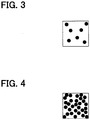
- FIG. 3 conceptually illustrates a filling amount of the electrically conductive composition in the base pattern 21.
- a result of a simulation of the electrical conductivity of the base pattern 21 having a transmittance of 85% is 0.3 ⁇ 10 ⁇ 6 S/m.
- the highly electrically conductive pattern 22 is made of an ITO film filled with an electrically conductive composition (here, ITO) more densely than the transparent electrically conductive film constituting the base pattern 21.
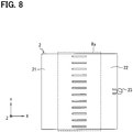
- FIG. 4 conceptually illustrates a filling amount of the electrically conductive composition in the highly electrically conductive pattern 22.
- the base pattern 21 and the highly electrically conductive pattern 22 do not necessarily have to be made of the same electrically conductive composition.
- the base pattern 21 and the highly electrically conductive pattern 22 may be made of different electrically conductive compositions.
- the base pattern 21 may be a GZO film.
- Each of the plurality of highly electrically conductive patterns 22 is formed in a straight line shape having a predetermined width W2.
- the width W2 of the highly electrically conductive pattern 22 may be set to a value smaller than the resolution of human eyes. Although the resolution of human eyes itself, of course, varies between individuals, an assumed value of the resolution of human eyes is set to 50 ⁇ m in the present embodiment. That is, the highly electrically conductive pattern 22 is an electrically conductive member having a straight line shape in which the width W2 is set to 50 ⁇ m or less. For example, the width W2 of the highly electrically conductive pattern 22 is set to 30 ⁇ m. FIG. 1 and the like illustrate the width W2 of the highly electrically conductive pattern 22 in an exaggerated manner.
- a length L2 of the highly electrically conductive pattern 22 may be set to, for example, a length electrically corresponding to ⁇ /4.
- FIGS. 5A and 5B illustrate a result of a simulation of a current distribution during resonance in a patch antenna in which the entire faces of a patch pattern and a ground pattern are made of a transparent conductor film having a transmittance of 80% and an electrical conductivity of 0.3 ⁇ 10 ⁇ 6 S/m.
- current flows parallel to the X axis during resonance and the intensity of the current is highest in a central region in the X-axis direction. That is, current contributing to the radiation of radio waves is concentrated on the central region in the X-axis direction.
- the resonance current flowing direction is also referred to as the resonance current direction.
- the resonance current direction is parallel to the X axis.
- a central region Rx of the patch pattern 2 may be within a predetermined distance Dx in the X-axis direction from a line segment Mx which is located on the middle in the X-axis direction.
- the central region Rx of the patch pattern 2 is a region in which the current intensity is equal to or higher than 1/ ⁇ 2 of the maximum amplitude.
- the region in which the current intensity is equal to or higher than 1/ ⁇ 2 of the maximum amplitude may be identified by a simulation.
- the plurality of highly electrically conductive patterns 22 are arranged side by side in the Y-axis direction in such a manner that each of the highly electrically conductive patterns 22 extends across the central region Rx of the patch pattern 2 (in other words, in parallel to the X-axis direction).
- An interval Lp between the highly electrically conductive patterns 22 is appropriately designed taking into consideration a required radiant gain and the transparency (in other words, the transmittance) of the entire patch pattern.
- the width W2 of the highly electrically conductive pattern 22 is set to a value with which the highly electrically conductive pattern 22 is almost invisible by human eyes.
- the highly electrically conductive pattern 22 is an electrically conductive member having a transmittance of 0%, when the pattern interval Lp is set to a relatively small value to densely arrange the plurality of highly electrically conductive patterns 22, the transmittance may be reduced as a whole.
- the pattern interval Lp is preferably set to, for example, 200 ⁇ m.
- the ground pattern 3 is an electrically conductive member formed in a thin-film shape.
- the ground pattern 3 has the same size as the patch pattern 2 or is larger than the patch pattern 2.
- the ground pattern 3 is electrically connected to an external conductor of the coaxial cable to provide a ground potential in the patch antenna.
- the ground pattern 3 is provided with a base pattern 31 which is made of a transparent electrically conductive film and a plurality of highly electrically conductive patterns 32 which is made of an electrically conductive film having a higher electrical conductivity than the transparent electrically conductive film in a manner similar to the patch pattern 2.
- the base pattern 31 of the ground pattern 3 has a configuration similar to the configuration of the base pattern 21 of the patch pattern 2.
- the highly electrically conductive pattern 32 of the ground pattern 3 has a configuration similar to the configuration of the highly electrically conductive pattern 22 of the patch pattern 2.
- the highly electrically conductive pattern 32 corresponds to a ground side highly electrically conductive pattern.
- the highly electrically conductive patterns 32 of the ground pattern 3 are preferably arranged at positions facing the respective highly electrically conductive patterns 22 of the patch pattern 2. Such a mode makes it possible to further increase the current intensity.
- the antenna module 100 configured as described above is driven by the principle of operation similar to the patch antenna to transmit and receive the target radio wave.
- FIG. 6 illustrates a result of a measurement of the transparency (in other words, the transmittance) of the entire antenna module 100 in the visible light region when the pattern interval Lp is adjusted in the antenna module 100.
- the transmittance of the entire antenna module 100 corresponds to the transmittance of a configuration in which the patch pattern 2, the transparent base 1, and the ground pattern 3 are stacked.
- An additional highly electrically conductive pattern 22 is arranged in a space generated by reducing the pattern interval Lp. That is, in the patch pattern 2, the number of highly electrically conductive patterns 22 arranged side by side in the Y-axis direction corresponds to an integer part of a value obtained by dividing the length L1Y in the Y-axis direction by the pattern interval Lp.
- the configuration of the present embodiment makes it possible to achieve a transmittance of 75% or higher when the pattern interval Lp is set to any value in the range of 150 ⁇ m to 400 ⁇ m.
- a transmittance of approximately 80% is achieved.
- the reason why the entire transmittance decreases as the pattern interval Lp is narrowed is that the number of highly electrically conductive patterns 22 arranged on the patch pattern 2 increases to increase the ratio of opaque highly electrically conductive patterns 22 in the patch pattern 2.
- FIG. 7 illustrates a result of a simulation of the gain of the antenna module 100 when the pattern interval Lp is adjusted in the antenna module 100.
- a solid line in FIG. 7 indicates the gain of the antenna module 100.
- a dot-dash line in FIG. 7 indicates a gain (specifically, 6.3 dBi) in a conventional patch antenna in which a patch pattern and a ground pattern are formed of copper foil having an electrical conductivity of 58 ⁇ 10 ⁇ 6 S/m as a first comparative configuration.
- a two-dot chain line in FIG. 7 indicates a gain (specifically, 0.5 dBi) in a patch antenna in which the entire faces of a patch pattern and a ground pattern are made of a transparent conductor film having a transmittance of 80% and an electrical conductivity of 0.3 ⁇ 10 ⁇ 6 S/m as a second comparative configuration.
- Each of the antenna modules as the first and second comparative configurations is configured to operate as a patch antenna at the same frequency as the antenna module 100, and the position of the feeding point and the dimension of each member are the same as those of the antenna module 100.
- the present embodiment makes it possible to achieve a gain of 4 dBi or more by setting the pattern interval Lp to 200 ⁇ m or less.
- the antenna module 100 which provides a gain of 4.2 dBi can be obtained.
- the gain of the second comparative configuration which has a transmittance of 80% is 0.5 dBi.
- the configuration in which the pattern interval Lp is set to 200 ⁇ m in the antenna module 100 can achieve a gain 3.7 dB higher than the gain of the second comparative configuration.
- the configuration in which the pattern interval Lp is set to 200 ⁇ m in the antenna module 100 has a transmittance of approximately 80%. That is, the configuration of the present embodiment makes it possible to increase the gain by 3.7 dB while achieving the transmittance of the same level as the second comparative configuration.
- the antenna module 100 of the present embodiment achieves a transmittance of 75% or higher, the antenna module 100 can be used in a state affixed to a windshield of a vehicle.
- the antenna module 100 of the present embodiment is suitable not only for transmission and reception of radar waves, but also as an antenna that is affixed to the windshield and used for receiving radio waves arriving from the outside of the vehicle in a zenith direction or a horizontal direction.
- the antenna module 100 is also suitable as an antenna for communicating with a roadside device, an antenna for receiving radio waves from a navigation satellite, or an antenna for receiving radio broadcast waves.
- the gain of the antenna can be increased by arranging the linear electrically conductive members having a relatively high electrical conductivity (that is, the highly electrically conductive patterns 22) along the direction of current induced by the patch pattern as the radiating element. Further, the transmittance of the entire antenna module 100 can be maintained at a high level by forming each of the highly electrically conductive patterns 22 with a thinness that is difficult to visually recognize and setting the interval Lp between the highly electrically conductive patterns 22 to a value sufficiently larger than the width W2 of the highly electrically conductive patterns 22. That is, the configuration disclosed as the present embodiment makes it possible to achieve both a high gain and a high transmittance of the antenna.
- the highly electrically conductive patterns 32 each having a fine-linear shape are arranged at predetermined intervals on the ground pattern 3 which provides the ground potential.
- Such a configuration makes it possible to increase the gain as compared to a configuration in which the highly electrically conductive patterns 22 are arranged only on the patch pattern 2.
- the length of the highly electrically conductive patterns 22 is set so that the highly electrically conductive patterns 22 extend across the central region Rx of the patch pattern 2.
- a component that has the same function as the component described in a preceding embodiment is assigned with the same reference numeral, and the redundant explanation is omitted.
- a preceding embodiment may be applied to the other parts of the configuration.
- the above embodiment discloses the mode in which the highly electrically conductive patterns 22 extend across the central region Rx of the patch pattern 2 (in other words, the highly electrically conductive patterns 22 are sufficiently long).
- the present disclosure is not limited thereto. It is only required that the highly electrically conductive patterns 22 be locally arranged along the resonance current direction in a part where a strong current flows.
- the length L2 of the highly electrically conductive patterns 22 may be set relatively short.
- the length L2 of the highly electrically conductive patterns 22 may be set to electrically 1/8 or 1/10 of the target wavelength.
- the highly electrically conductive patterns 22 may be formed in a curved shape or a bent shape. Further, it is only required that the highly electrically conductive patterns 22 be made of a member having a higher electrical conductivity than the base pattern 21. Thus, the highly electrically conductive patterns 22 do not necessarily have to be an ITO film that is filled with an electrically conductive composition so as to have a transmittance of 0%. For example, a transparent electrically conductive film having a transmittance of 25% or 50% may be used.
- the above embodiment discloses the configuration in which the highly electrically conductive patterns 32 are arranged on the ground pattern 3.
- the present disclosure is not limited thereto.
- a configuration in which no highly electrically conductive pattern 32 is arranged on the ground pattern 3 can also be employed.
- the above embodiment discloses the configuration in which the transparent electrically conductive film made of a granular (powdered) electrically conductive composition is employed as the transparent electrically conductive film for constituting the base patterns 21, 31.
- the transparent electrically conductive film as the base patterns 21, 31 may be a transparent electrically conductive film including an electrically conductive member having a wire shape (e.g., a silver nanowire) as the electrically conductive composition as illustrated in FIG. 10 .
- an electrically conductive member having a wire shape e.g., a silver nanowire
- metals such as gold, copper, platinum, tin, aluminum, iron, and nickel, and various alloy materials can be employed as the electrically conductive member having a wire shape.
- Each of the highly electrically conductive patterns 22 may be not an electrically conductive film, but a conductor having a fine-linear shape.
- the fine line indicates a line having a width of 50 ⁇ m or less.
- the above embodiment discloses, as the configuration of the patch pattern 2, the configuration in which the base pattern 21 and the highly electrically conductive patterns 22 are arranged in such a manner that the base pattern 21 and the highly electrically conductive patterns 22 do not overlap each other.
- the present disclosure is not limited thereto.
- the highly electrically conductive patterns 22 may be arranged on the base pattern 21 so that the base pattern 21 and the highly electrically conductive patterns 22 overlap each other. The same applies to the ground pattern 3.
- the above embodiment discloses the mode in which the present disclosure is applied to the patch antenna.
- the present disclosure is not limited thereto.
- the present disclosure is applicable to various antenna modules such as a dipole antenna and an inverted F antenna.
- a transparent electrically conductive film may be used as a principal constituent element of a linear element 4 included in the dipole antenna, and highly electrically conductive patterns 41 may be arranged on edges along the longitudinal direction as illustrated in FIG. 12 .
- the highly electrically conductive pattern 41 is a configuration having a technical significance similar to the highly electrically conductive pattern 22 in the above embodiments.
- the highly electrically conductive pattern 41 may extend from a feeding point to the other end on the central part of the linear element 4.
- FIGS. 12 and 13 illustrate the width of the linear element 4 and the width of the highly electrically conductive pattern 41 in an exaggerated manner.
- the antenna module 100 is used in a state affixed to the inner face of a windshield 10 of the vehicle in an attitude in which the transmission and reception direction of the target radio wave faces the outside of the cabin.
- the attitude in which the transmission and reception direction of the target radio wave faces the outside of the cabin indicates, for example, an attitude in which the direction of the center of the directivity faces the outside of the cabin.
- the attitude in which the transmission and reception direction of the target radio wave faces the outside of the cabin substantially corresponds to an attitude in which the patch pattern 2 faces the outside of the cabin.
- the antenna module 100 is capable of transmitting a signal from the windshield 10 toward the outside of the cabin (that is, toward the front of the vehicle). Further, with the above mounting attitude, the antenna module 100 is capable of receiving a radio wave arriving from the front of the vehicle.
- the antenna module 100 may be used in only either one of transmission or reception.
- the transmission and reception direction of the antenna module 100 corresponds to the direction in which the antenna module 100 operates (hereinbelow, the operating direction).
- the mounting surface in the following description indicates a surface to which the antenna module 100 is affixed. Specifically, the mounting surface indicates a part of the inner face of the windshield 10 to which the antenna module 100 is affixed.
- a second transparent base 5 is stacked on the upper side of the patch pattern 2.
- the transparent base 1 is also referred to as the first transparent base 1.
- the configuration in which the second transparent base 5 is disposed on the patch pattern 2 corresponds to a configuration in which an intermediate layer is disposed between the windshield 10 which serves as the mounting surface for the antenna module 100 and the patch pattern 2.
- the second transparent base 5 is used for adjusting the separation distance between the windshield 10 and the patch pattern 2 to prevent a reduction in a gain caused by a reflected wave generated on the windshield 10.
- the gain described herein mainly indicates a gain in the direction from the ground pattern 3 to the patch pattern 2 (hereinbelow, the perpendicular-to-antenna direction).
- a thickness Tn of the second transparent base 5 is set to, for example, a value electrically corresponding to half the target wavelength (that is, the half wavelength, ⁇ /2).
- the value electrically corresponding to ⁇ /2 is an effective length taking the wavelength shortening effect obtained by the second transparent base 5 into consideration. If the relative dielectric constant of the second transparent base 5 is 2.3, the wavelength of the target radio wave within the second transparent base 5 is 8.3 mm.
- the configuration in which the thickness Tn of the second transparent base 5 is set to the value electrically corresponding to ⁇ /2 is a configuration in which the thickness Tn is set to approximately 4.15 mm.
- the thickness Tn of the second transparent base 5 may be set to an integral multiple of (e.g., twice or three times) the value electrically corresponding to ⁇ /2.
- the above setting of the thickness Tn of the second transparent base 5 is performed by focusing on the point that the gain as an antenna varies according to the thickness Tn of the second transparent base 5. That is, when the thickness Tn is set to a value electrically corresponding to 0.75 ⁇ , a reflected wave generated on the mounting surface acts in the direction cancelling a direct wave to reduce the gain as an antenna. On the other hand, when the separation distance between the patch pattern 2 and the mounting surface is set to electrically an integral multiple of half the target wavelength, the reflected wave is in phase with the direct wave. Thus, it is possible to prevent a reduction in the gain caused by the reflected wave.
- the expression of "0.75 ⁇ " indicates a value obtained by multiplying the wavelength of the target radio wave by 0.75.
- the expression of "0.5 ⁇ ” indicates a value obtained by multiplying the target wavelength by 0.5.
- the expression of "0.5 ⁇ ” has the same meaning as " ⁇ /2" described above.
- FIG. 16 illustrates a result of a simulation of the relationship between the separation distance between the patch pattern 2 and the windshield 10 and the gain in a configuration in which a space between the patch pattern 2 and the windshield 10 is hollow.
- the gain of the antenna module 100 becomes highest.
- the second transparent base 5 whose thickness Tn is an integral multiple of a value electrically corresponding to 0.5 ⁇ be disposed on the upper side of the patch pattern 2.
- the dielectric constant of the windshield 10 as the mounting surface differs by approximately 10% from a target value specified as a product specification, it is possible to provide a gain substantially equal to a gain in a case where the dielectric constant of the windshield 10 as the mounting surface is equal to the target value. That is, it is possible to increase the robustness with respect to variations in the dielectric constant of the windshield 10 as the mounting surface.
- the target value corresponds to a target value on manufacture (in other words, the design value).
- the mode in which the antenna module 100 is used in a state affixed to the inner face of the windshield 10 has been described above.
- a usage mode of the antenna module 100 is not limited thereto.
- the antenna module 100 may be used in a state affixed to the inner face of a rear glass or a glass as a window disposed on the side face part of the vehicle (hereinbelow, the side glass).
- the windshield 10, the rear glass, and the side glass correspond to a window glass.
- the window glass is, for example, a transparent member that closes a window disposed on the vehicle, such as a front window, a window disposed on the side face part of a vehicle Hv (so-called the side window), or a rear window.
- the principal material of the window glass is not limited to glass.
- the window glass may be made of resin having a predetermined transmittance. That is, the configuration corresponding to the window glass such as the windshield 10 may be made of resin glass.
- the antenna module 100 can also be affixed to the inner face of the windshield 10 in an attitude in which the operating direction faces the inside of the vehicle.
- the antenna module 100 is configured as an antenna for receiving a radio wave of Bluetooth (registered trademark) or Wi-Fi (registered trademark)
- the configuration in which the antenna module 100 is affixed to the upper end of the windshield 10 in an attitude in which the operating direction faces the inside of the cabin easily receives a radio wave from a mobile terminal such as a smartphone carried into the cabin by a user.
- the antenna module 100 can employ a configuration disclosed below as an eighth modification.
- the antenna module 100 according to the eighth modification corresponds to a modification of the configuration disclosed in the seventh modification.
- the antenna module 100 of the eighth modification is provided with the transparent base 1, the patch pattern 2, the ground pattern 3, and the second transparent base 5.
- FIG. 17 is an exploded perspective view of the antenna module 100 in the present modification. The technical significance of each member is as described in the first embodiment and the various modifications.
- the first transparent base 1 and the second transparent base 5 in the present modification are larger than the patch pattern 2 as illustrated in FIG. 17 .
- the length in the X-axis direction of the first transparent base 1 and the second transparent base 5 is set to three times the length in the X-axis direction of the patch pattern 2.
- the length in the Y-axis direction of the first transparent base 1 and the second transparent base 5 is set to three times the length in the Y-axis direction of the patch pattern 2.
- the scaling factor of the dimension in each direction can be appropriately changed and is not limited to the above example.
- the length in the Y-axis direction of the first transparent base 1 and the second transparent base 5 may be set to 1.5 times or twice the length in the Y-axis direction of the patch pattern 2.
- the ground pattern 3 is formed over the entire back face of the first transparent base 1.
- the ground pattern 3 may be locally formed on the back face of the first transparent base 1. It is only required that the ground pattern 3 be formed in a part facing the patch pattern 2 in the first transparent base 1.
- the second transparent base 5 includes slits 52a, 52b each of which has a straight line shape.
- the slits 52a, 52b are formed parallel to the Y axis on the left side and the right side of an antenna contact part 51 which comes into contact with the patch pattern 2.
- Each of the slits 52a, 52b is a cut-away structure.
- the slit 52 corresponds to an opening that exposes the patch pattern 2 or the first transparent base 1 which is formed directly below the second transparent base 5.
- the left side of the antenna contact part 51 indicates the negative side in the X-axis direction.
- the right side of the antenna contact part 51 indicates the positive side in the X-axis direction.
- the resonance current direction in the configuration of the present modification is parallel to the X axis. That is, the above formation mode of the slits 52a, 52b corresponds to an example of a configuration in which the slits 52a, 52b are formed perpendicularly to the resonance current direction.
- the slit 52a is a slit 52 that is formed on the left side of the antenna contact part 51.
- the slit 52b is a slit 52 that is formed on the right side of the antenna contact part 51.
- the slits 52a, 52b are referred to as the slits 52.
- Each of the slits 52 is formed at a position whose distance from the antenna contact part 51 electrically corresponds to 0.5 ⁇ . That is, a separation distance Sp in the X-axis direction between the antenna contact part 51 and the slit 52 is set to a value electrically corresponding to 0.5 ⁇ .
- the width of the slits 52 may be appropriately set.
- the length of the slits 52 may be set equal to or longer than the length in the Y-axis direction of the antenna contact part 51.
- Each of the slits 52 is formed in such a manner that the center point thereof is located on a straight line that is parallel to the X axis and passes through the center of the antenna contact part 51. That is, the two slits 52 are disposed to sandwich the antenna contact part 51 in the resonance current direction.
- Such a configuration makes it possible to prevent a reduction in the gain that occurs when the antenna module 100 is used in a state affixed to the windshield 10 by an action as described below.
- the second transparent base 5 is interposed as an intermediate layer between the mounting surface and the patch pattern 2
- some of the radio waves emitted by the patch pattern 2 are repeatedly reflected by member boundary surfaces and propagate from the central part to the right and left sides within the second transparent base 5. That is, a surface wave may be formed within the second transparent base 5 as the intermediate layer.
- the member boundary surfaces include the mounting surface and the surface of the patch pattern 2. It is desired for the antenna module 100 to form the directivity to the outside of the windshield 10. Thus, such a surface wave reduces the gain.
- the slits 52 function as elements (so-called choke) that block propagation of radio waves.
- the slits 52 function as elements (so-called choke) that block propagation of radio waves.
- a gap between the first transparent base 1 and the second transparent base 5 which may be formed around the patch pattern 2 due to the thickness of the patch pattern 2 may be filled with a material similar to the material of the first transparent base 1.
- the gap between the first transparent base 1 and the second transparent base 5 which may be formed around the patch pattern 2 may be filled with a material similar to the material of the second transparent base 5.
- the gap between the first transparent base 1 and the second transparent base 5 which may be formed around the patch pattern 2 may be filled with a transparent material that differs from both the material of the first transparent base 1 and the material of the second transparent base 5.
- the gap between the first transparent base 1 and the second transparent base 5 which may be formed around the patch pattern 2 may be hollow.
- the second transparent base 5 may be stacked on the first transparent base 1 provided with the patch pattern 2. That is, the first transparent base 1 and the second transparent base 5 may be directly joined together around the patch pattern 2.
- the antenna module 100 as the light-transmissive antenna described above can be employed as, for example, an antenna of a communication module that is used in a state affixed to the inner face of the windshield 10 of the vehicle (hereinbelow, the window affixing type communication module).
- the window affixing type communication module an antenna of a communication module that is used in a state affixed to the inner face of the windshield 10 of the vehicle.
- a window affixing type communication module 200 to which the configuration of the above antenna module 100 is applied will be described.
- the window affixing type communication module 200 is provided with an antenna module 100A and a signal processor 6.
- the antenna module 100A corresponds to, for example, the antenna module 100 according to the eighth modification.
- the antenna module 100A is provided with a plurality of patch patterns 2 as described below. That is, the antenna module 100A is provided with a plurality of antennas.
- the signal processor 6 executes predetermined signal processing on a signal received by the antenna module 100A.
- the signal processor 6 is provided with, for example, a demodulator circuit which demodulates a received signal.
- the signal processor 6 may be provided with a drive circuit which supplies high-frequency power to the antenna module 100 to cause the antenna module 100A to transmit a radio signal.
- the signal processor 6 may be provided with a function of detecting an object by analyzing signals received by the plurality of antennas (hereinbelow, the object detecting function). For example, the signal processor 6 transmits radio waves as probing waves from the antenna module 100A and receives radio waves which are the probing waves reflected by an object by the plurality of antennas included in the antenna module 100A. The signal processor 6 estimates the distance from the object to be detected and the position of the object on the basis of a phase difference and the strength of the signals received by the respective antennas. Various configurations and algorithms can be employed as a configuration and an algorithm for detecting an object on the basis of the received signals.
- the signal processor 6 includes one or more dedicated ICs and various analog circuit elements.
- the signal processor 6 may include a computer provided with a CPU, a RAM, and a ROM.
- the computer which constitutes the signal processor 6 may include an MPU or a GPU instead of the CPU.
- the computer may include a CPU, an MPU, a GPU, and an IC in combination.
- the signal processor 6 is electrically connected to the antenna module 100A through a communication cable 7 such as a coaxial cable or a flexible cable.
- the signal processor 6 is connected to an external device (e.g., a predetermined electronic control unit (ECU)) through a predetermined communication cable 8.
- ECU electronice control unit
- a connector 101 for connection with the communication cable 7 is formed on the end of the antenna module 100A.
- the antenna module 100A is connected to the signal processor 6 through the connector 101 and the communication cable 7.
- the communication cable 7 is provided with a ground line which provides a ground potential and a signal line through which a signal flows.
- the communication cable 7 serves as a feeding cable for the antenna module 100A.
- the antenna module 100A is provided with a first transparent base layer L1, a radiating element layer L2 which is disposed on the upper side of the first transparent base layer L1, a ground layer L3 which is disposed on the lower side of the first transparent base layer L1, and a second transparent base layer L4 which is disposed on the upper side of the radiating element layer L2.
- White arrows in FIG. 19 indicate transmission and reception directions of the antenna module 100A.
- the first transparent base layer L1 corresponds to the first transparent base 1 described above.
- Various materials can be employed as the material of the first transparent base layer L1 as described in the first embodiment.
- the radiating element layer L2 is provided with at least one patch pattern 2.
- the radiating element layer L2 is provided with four patch patterns 2 as illustrated in FIG. 20 .
- the four patch patterns 2 are arranged in a row in parallel to the Y axis on the central part in the X-axis direction of the radiating element layer L2.
- a part of the radiating element layer L2 excepting the patch patterns 2 may be filled with a material similar to the material of the first transparent base layer L1 or the material of the second transparent base layer L4.
- the part of the radiating element layer L2 excepting the patch patterns 2 may be filled with a transparent material that differs from both the material of the first transparent base 1 and the material of the second transparent base 5 or may be hollow.
- the second transparent base layer L4 may be stacked after arranging the patch patterns 2 at predetermined positions on the first transparent base layer L1. The number and the arrangement mode of patch patterns 2 included in the radiating element layer L2 can be appropriately changed.
- Each of the patch patterns 2 is electrically connected to the signal line of the communication cable 7 through the connector 101.
- the length in the X-axis direction of each of the patch patterns 2 is set to a length electrically corresponding to 0.5 ⁇ .
- Each of the patch patterns 2 is configured to operate as a patch antenna. The resonance current flows in the X-axis direction in the patch pattern 2.
- the ground layer L3 is a layer on which a transparent electrically conductive film as the ground pattern 3 is disposed.
- the ground pattern 3 as the ground layer L3 is formed over the entire back face of the first transparent base layer L1.
- the ground layer L3 is electrically connected to the signal line of the communication cable 7, the signal line providing the ground potential, through the connector 101.
- the ground pattern 3 as the ground layer L3 may be locally formed on the back face of the first transparent base layer L1 including a part facing the patch patterns 2 of the radiating element layer L2.
- the second transparent base layer L4 corresponds to the second transparent base 5 described in the seventh modification and the eighth modification.
- the second transparent base layer L4 is also made of any transparent dielectric material. Various materials can be employed as the material of the first transparent base layer L1 and the material of the second transparent base layer L4.
- a thickness TnA of the second transparent base layer L4 is set to a value electrically corresponding to 0.5 ⁇ on the basis of the technical idea described in the seventh modification.
- the value corresponding to 0.5 ⁇ indicates a value within a predetermined allowable range determined based on 0.5 ⁇ such as 0.5 ⁇ ⁇ 0.1 ⁇ .
- the expression of "0.1 ⁇ " indicates a length obtained by multiplying the wavelength of the target radio wave by 0.1.
- the allowable range corresponds to a range in which an effect of preventing a gain reduction caused by a reflected wave on a glass surface (in other words, the gain increasing effect) can be obtained.
- the thickness TnA of the second transparent base layer L4 may be set to electrically an integral multiple (e.g., twice or three times) of half the target wavelength.
- the second transparent base layer L4 includes slits 52 each of which has a straight line shape.
- the slits 52 are formed along the Y-axis direction on lateral sides of a plurality of antenna contact parts 51 which come into contact with the respective patch patterns 2.
- the two slits 52 are formed to sandwich the plurality of antenna contact parts 51 which are arranged in a row along the Y-axis direction.
- the formation mode of the slits 52 corresponds to an example of the configuration in which the slits 52a, 52b are formed perpendicularly to the resonance current flow direction in the patch pattern 2.
- a separation distance Sp between each of the slits 52 and the antenna contact parts 51 is set to a value electrically corresponding to 0.5 ⁇ .
- FIG. 21 discloses, as an example, a mode in which each of the slits 52 is continuously formed.
- the slit 52 may be intermittently formed (in other words, formed in a broken line shape).
- FIG. 22 illustrates a result of a simulation of an electric field strength on the boundary surface between the second transparent base layer L4 and the windshield 10 in the configuration including no slit 52 (hereinbelow, the comparative configuration).
- FIG. 23 illustrates a result of a simulation of an electric field strength on the boundary surface between the second transparent base layer L4 and the windshield 10 in the configuration including the slits 52 (that is, the configuration of the present embodiment).
- FIG. 24 illustrates a result of a simulation of the directivity in each of the comparative configuration and the configuration of the present embodiment.
- a solid line in FIG. 24 indicates the directivity in the configuration of the present embodiment, that is, the configuration in which the second transparent base layer L4 is provided with the slits 52.
- a solid line in FIG. 24 indicates the directivity in the comparative configuration.
- the antenna modules 100, 100A described above can be used as an antenna for transmitting and receiving a probing wave in a radar device (e.g., a millimeter wave radar) as described in the beginning of the first embodiment.
- a periphery monitoring unit 300 which is provided with the antenna module 100A as an antenna for transmitting and receiving a probing wave will be described with reference to the drawings.
- the periphery monitoring unit 300 is provided with a camera 310, a radar device 320, and a housing 330.
- the camera 310 is a device that captures an image of a unit front side.
- the unit front side indicates the front side for the periphery monitoring unit 300.
- the front, rear, right, and left for the periphery monitoring unit 300 is previously set with respect to the periphery monitoring unit 300.
- the front side for the periphery monitoring unit 300 corresponds to an imaging direction of the camera 310 in another point of view.
- a broken line in FIG. 25 conceptually indicates an imaging range (in other words, the field of view) of the camera 310.
- the periphery monitoring unit 300 is used in a state attached to the upper end of a windshield 10 of a vehicle near a rearview mirror in an attitude in which the camera 310 captures an image of the front side outside a cabin.
- the radar device 320 transmits a radio wave having a predetermined frequency as a probing wave toward the unit front side and receives a reflected wave which is the probing wave reflected by an object to detect the object.
- the radar device 320 is provided with the antenna module 100A and a signal processor 6A.
- the antenna module 100A and the signal processor 6A are capable of communicating with each other using a connector 101 and a communication cable 7.
- the signal processor 6A is provided with a drive circuit for supplying high-frequency current to the antenna module 100A to cause the antenna module 100A to transmit the probing wave. Further, the signal processor 6A is provided with a function of generating data indicating the position of an object by analyzing a signal received by the antenna module 100A.
- the housing 330 houses the camera 310 and the signal processor 6A therein.
- the housing 330 is provided with a mount 331.
- the mount 331 is a configuration for attaching the periphery monitoring unit 300 to a predetermined position inside the cabin.
- the present embodiment discloses, as an example, a mode in which the periphery monitoring unit 300 is attached to a ceiling inside the cabin near a joint part between the ceiling and the windshield.
- the periphery monitoring unit 300 may be attached to the inner face of the windshield 10.
- the periphery monitoring unit 300 may be attachable to the rearview mirror.
- the periphery monitoring unit 300 may be mountable on the upper end of an instrument panel.
- the periphery monitoring unit 300 may be attached to any position near a rear glass in an attitude in which the unit front side faces the vehicle rear direction.
- the front side part (hereinbelow, the front face part) of the housing 330 of the present embodiment is formed in an open shape so that the camera 310 is capable of capturing an image of the unit front side. That is, the housing 330 is provided with an opening for the camera 310 to capture an image of the unit front side on the front face part thereof.
- the antenna module 100A having a predetermined hardness (hereinbelow, the target hardness) is disposed in the opening of the housing 330 so that the antenna module 100A functions as a partition that separates the inside and the outside of the housing 330.
- Such a configuration corresponds to a configuration in which the antenna module 100A as the light-transmissive antenna is disposed within the imaging range of the camera.
- the antenna module 100A is transparent.
- the antenna module 100A inserted in the front face part of the housing 330 functions as a window for the camera 310 to capture an image of the outside of the unit.
- the antenna module 100A is transparent, even when the antenna module 100A is present in front of the camera 310 (that is, in the imaging range), the antenna module 100A is less likely to affect a recognition accuracy of a predetermined ECU when the ECU performs an object recognition based on an image captured by the camera 310.
- the antenna module 100A inserted in the front face part of the housing 330 functions as the window for the camera 310 and also serves as a member that protects a stored object such as the camera 310.
- the configuration in which the antenna module 100A is inserted in the front face part of the housing 330 so as to function as the partition that separates the inside and the outside of the housing 330 corresponds to a configuration in which the antenna module 100 is used as the front face part of the housing 330.
- the antenna module 100A serves as an antenna for transmitting and receiving the probing wave by the radar device 320.
- the antenna module 100A having the target hardness for example, includes the second transparent base layer L4 formed of a resin material having the target hardness.
- the antenna module 100A having the target hardness may include the first transparent base layer L1 formed of a resin material having the target hardness.
- the above configuration corresponds to a configuration in which an antenna for transmitting and receiving the probing wave is disposed on the front face of the camera 310 in a unit in which the camera 310 and the radar device 320 are integrated.
- the antenna module 100A as the antenna for transmitting and receiving the probing wave is transparent.
- the antenna module 100A is less likely to obstruct the object recognition based on an image captured by the camera 310.
- the antenna module 100A is disposed within the viewing angle of the camera 310. Thus, it is possible to reduce the size of the periphery monitoring unit 300 in which the camera 310 and the radar device 320 are integrated.
- the antenna module 100A is used as a part of the housing 330.
- the present disclosure is not limited thereto.
- the antenna module 100A may be affixed to the inner face of the windshield 10.
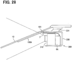
- the disposition mode of the signal processor 6A and the camera 310 inside the housing 330 can be appropriately changed.
- the signal processor 6A may be disposed on the lateral side of the camera 310 as illustrated in FIG. 27 or may be disposed on the back side of the camera 310 as illustrated in FIG. 28 .
Abstract
Description
- This application is based on Japanese Patent Application No.
2017-074636 filed on April 4, 2017 2018-062699 filed on March 28, 2018 - The present disclosure relates to a light-transmissive antenna which is optically transparent antenna, a window affixing type communication module using the light-transmissive antenna, and a periphery monitoring unit including the light-transmissive antenna as an antenna for transmitting and receiving a probing wave.
-
Patent Literature 1 proposes a light-transmissive antenna, in which a transparent film made of an electrically conductive composition such as tin-doped indium oxide (so-called transparent electrically conductive film) is disposed on a transparent base such as glass so that the transparent electrically conductive film functions as a radiating element. - Patent Literature 1 :
JP 2009-533888 A - Typically, the transmittance of light (mainly, visible light) and the electrical conductivity of a transparent electrically conductive film are in a trade-off relationship. That is, as the transmittance is increased, the electrical conductivity is reduced. For example, the electrical conductivity of a transparent electrically conductive film having a transmittance of 80% or higher is two or more orders of magnitude lower than the electrical conductivity of copper foil.
- Thus, an antenna that uses a transparent electrically conductive film having a transmittance of 80% as a radiating element instead of copper foil has a considerably lower gain than an antenna that uses copper foil as a radiating element. In order to increase the gain, it is necessary to increase a filling density of the electrically conductive composition in the transparent electrically conductive film. However, in this case, the transmittance is reduced.
- The present disclosure has been made in view of the above circumstances, and an object thereof is to provide a light-transmissive antenna, a window affixing type communication module, and a periphery monitoring unit that make it possible to increase the gain while preventing a reduction in the transmittance.
- According to an aspect of the present disclosure, a light-transmissive antenna includes: a transparent base made of a transparent insulating material; an antenna pattern formed on the transparent base, the antenna pattern being made of a transparent electrically conductive film that is a film-like member having a predetermined transmittance and a predetermined electrical conductivity; and a plurality of highly electrically conductive patterns arranged on the antenna pattern. Each of the highly electrically conductive patterns is made of an electrically conducive member having a higher electrical conductivity than the transparent electrically conductive film and formed in a linear shape. Each of the plurality of highly electrically conductive patterns has a predetermined width set equal to or smaller than a value assumed as a resolution of human eyes.
- According to the above configuration, the highly electrically conductive patterns having a relatively high electrical conductivity are arranged on a part of the antenna pattern which is made of the transparent electrically conductive film. Thus, it is possible to increase the intensity of current flowing during a drive and increase the gain as compared to a configuration as an assumed configuration in which an antenna pattern is made of only a transparent electrically conductive film. Further, the width of each of the highly electrically conductive patterns arranged on the antenna pattern is set equal to or smaller than the assumed value (e.g., 50 µm) of the resolution of human eyes. Thus, since the part of the antenna pattern includes the highly electrically conductive patterns, it is possible to prevent a reduction in the transmittance of the entire antenna pattern. That is, the above configuration makes it possible to increase the gain while preventing a reduction in the transmittance.
- According to an aspect of the present disclosure, a window affixing type communication module includes: an antenna module which is the above-described light-transmissive antenna; and a signal processor that executes predetermined signal processing on a signal received by the antenna module. The antenna module is used in a state affixed to an inner face of a window glass of a vehicle.
- The window affixing type communication module uses the light-transmissive antenna. The above configuration makes it possible to increase the success rate of receiving radio waves arriving from the outside of the cabin while ensuring the visibility of a driver to the outside of the cabin.
- According to an aspect of the present disclosure, a periphery monitoring unit includes a camera, and a radar device that transmits a radio wave having a predetermined frequency as a probing wave and receives a reflected wave that is the probing wave reflected by an object to detect the object. The radar device includes: an antenna module which is the above-described light-transmissive antenna as an antenna for receiving the reflected wave; and a signal processor that executes predetermined signal processing on a signal received by the light-transmissive antenna to generate data indicating a position of the object. The antenna module is disposed on the front side of the camera at a position where at least a part of the antenna module is included in an imaging range of the camera.
- The periphery monitoring unit is provided with the light-transmissive antenna as an antenna for transmitting and receiving the probing wave. The antenna module is configured as the light-transmissive antenna. Thus, even when the antenna module is disposed within the imaging range of the camera, the antenna module is less likely to affect an image captured by the camera. Since the antenna module can be disposed within the imaging range of the camera, it is possible to downsize the periphery monitoring unit.
-
-
FIG. 1 is a top view of an antenna module according to a first embodiment. -
FIG. 2 is an enlarged view of a section taken along line II-II inFIG. 1 . -
FIG. 3 is a diagram conceptually illustrating a filling amount of an electrically conductive composition in a base pattern. -
FIG. 4 is a diagram conceptually illustrating a filling amount of an electrically conductive composition in a highly electrically conductive pattern. -
FIG. 5A is a diagram illustrating a current distribution in a patch pattern. -
FIG. 5B is a diagram illustrating the current distribution in the patch pattern. -
FIG. 6 is a graph illustrating a result of a test of the relationship between a pattern interval and a transmittance. -
FIG. 7 is a graph illustrating a result of an analysis of the relationship between the pattern interval and a gain. -
FIG. 8 is a diagram conceptually illustrating the configuration of a patch pattern in a first modification. -
FIG. 9 is a diagram for describing the configuration of an antenna module in a second modification. -
FIG. 10 is a diagram for describing the configuration of an antenna module in a third modification. -
FIG. 11 is a diagram illustrating an example of the configuration of an antenna module in a fifth modification. -
FIG. 12 is a diagram illustrating an example of the configuration of an antenna module in a sixth modification. -
FIG. 13 is a diagram illustrating an example of the configuration of the antenna module in the sixth modification. -
FIG. 14 is a diagram illustrating an example of a usage mode of the antenna module. -
FIG. 15 is a diagram for describing the configuration of an antenna module in a seventh modification. -
FIG. 16 is a graph illustrating a result of a simulation of the relationship between the distance from a mounting surface to the patch pattern and the gain. -
FIG. 17 is a diagram for describing the configuration of an antenna module in an eighth modification. -
FIG. 18 is a diagram for describing the configuration of a window affixing type communication module according to a second embodiment. -
FIG. 19 is a diagram for describing the configuration of an antenna module according to the second embodiment. -
FIG. 20 is a conceptual diagram illustrating the configuration of a radiating element layer of the second embodiment. -
FIG. 21 is a conceptual diagram illustrating the configuration of a second transparent base layer. -
FIG. 22 is a diagram illustrating a formation state of a surface wave in a comparative configuration. -
FIG. 23 is a diagram illustrating a formation state of a surface wave in the configuration of the second embodiment. -
FIG. 24 is a diagram illustrating an effect obtained by slits formed on the second transparent base layer. -
FIG. 25 is a block diagram illustrating a schematic configuration of a periphery monitoring unit according to a third embodiment. -
FIG. 26 is a conceptual diagram illustrating an example of an attachment mode of the periphery monitoring unit. -
FIG. 27 is a diagram conceptually illustrating the configuration of the periphery monitoring unit viewed from the front. -
FIG. 28 is a conceptual diagram illustrating an example of a modification of the configuration of the periphery monitoring unit. - Hereinbelow, a first embodiment will be described with reference to the drawings. An
antenna module 100 according to the present embodiment is configured to transmit and receive a radio wave having a predetermined frequency (hereinbelow, the target radio wave) by the principle of operation similar to a patch antenna. Theantenna module 100 may be used in only either one of transmission or reception. Theantenna module 100 corresponds to the light-transmissive antenna. - An operating frequency of the antenna module 100 (in other words, the frequency of the target radio wave) may be appropriately designed. In the present embodiment, as an example, the operating frequency is set to 24 GHz. For example, the
antenna module 100 can be used as an antenna for transmitting and receiving a probing wave in a radar device. The operating frequency of theantenna module 100 may be appropriately designed and may be, for example, 300 MHz, 760 MHz, 930 MHz, 1.575 GHz, 2.4 GHz, or 5.9 GHz as another mode. Hereinbelow, the wavelength of the target radio wave is also referred to as the target wavelength. In the present embodiment, since the frequency of the target radio wave is 24 GHz, the target wavelength is 12.5 mm. - The
antenna module 100 is, for example, connected to a radio device (not illustrated) through a coaxial cable. Signals received by theantenna module 100 are successively output to the radio device. Theantenna module 100 converts an electric signal input from the radio device to a radio wave and emits the radio wave to a space. The radio device uses a signal received by theantenna module 100 and supplies high-frequency power corresponding to a transmission signal to theantenna module 100. Theantenna module 100 and the radio device may be connected to each other through a matching circuit or a filter circuit instead of the coaxial cable. - Hereinbelow, the configuration of the
antenna module 100 will be described. - Hereinbelow, the specific configuration of the
antenna module 100 will be described. As illustrated inFIGS. 1 and 2 , theantenna module 100 is provided with atransparent base 1, apatch pattern 2, and aground pattern 3.FIG. 1 is a diagram illustrating the appearance of theantenna module 100 viewed from the upper direction (that is, a top view).FIG. 2 is a partially enlarged sectional view of theantenna module 100 taken along line II-II inFIG. 1 . The upper direction for theantenna module 100 is a direction from theground pattern 3 to thepatch pattern 2. - The
transparent base 1 is a plate-like member made of any transparent dielectric material (in other words, any electrical insulating material). The plate-like shape includes a thin-film shape such as a sheet shape or a film shape. The material of thetransparent base 1 may be appropriately selected taking into consideration the transparency in a visible light region, the heat resistance, and the mechanical strength. In the present embodiment, as an example, thetransparent base 1 is made of a resin film so as to have flexibility. - Various transparent materials including a polyester resin such as polyethylene terephthalate, an acrylic resin such as polymethyl methacrylate, a polycarbonate resin, a polyimide resin, a polyolefin resin such as a cycloolefin polymer, and a cellulosic resin such as triacetyl cellulose can be employed as resin of the resin film.
- In the present embodiment, the
transparent base 1 is configured to have a desired flexibility by using the resin film. However, the present disclosure is not limited thereto. Thetransparent base 1 may be made of a transparent rigid member such as glass, ceramics, or resin. - The
patch pattern 2 is disposed on one face of thetransparent base 1, and theground pattern 3 is disposed on the other face thereof. For convenience, hereinbelow, in thetransparent base 1, the face on which thepatch pattern 2 is disposed is referred to as a front face, and the face opposite to the front face is referred to as a back face. The direction from the back face to the front face in thetransparent base 1 corresponds to the upper direction for theantenna module 100. As illustrated in the sectional view ofFIG. 2 , thetransparent base 1 has a function of supporting thepatch pattern 2 and theground pattern 3 so that thepatch pattern 2 and theground pattern 3 face each other with a predetermined distance therebetween. The thickness of thetransparent base 1 is a parameter that should be appropriately designed. In the present embodiment, as an example, the thickness of thetransparent base 1 is set to 100 µm. - The size and the shape of the
transparent base 1 viewed from above (hereinbelow, the plane shape) may be a size and a shape that are necessary and sufficient for disposing a member such as thepatch pattern 2. In the present embodiment, as an example, thetransparent base 1 is formed in a rectangular shape. Alternatively, the shape of thetransparent base 1 may be a circular shape (including an elliptical shape) or other polygonal shapes. A material having a desired relative dielectric constant (e.g., 2.3) can be used as the material of thetransparent base 1. - The
patch pattern 2 is an electrically conductive member formed in a thin-film shape. Thepatch pattern 2 is formed in a rectangular shape in which the length of a pair of opposite sides electrically corresponds to 1/2 of the target wavelength (hereinbelow, λ/2). Here, "λ" indicates one wavelength of the target radio wave. Thepatch pattern 2 functions as a radiating element of the patch antenna. The electrical length described herein is an effective length taking into consideration a fringing electric field and a wavelength shortening effect by a dielectric. If the wavelength of the target radio wave is shortened by thetransparent base 1, the electric length may be half the shortened wavelength. - The present embodiment describes, as an example, a mode in which the plane shape of the
patch pattern 2 is set to a rectangular shape. However, the present disclosure is not limited thereto. As another mode, the plane shape of thepatch pattern 2 may be a circular shape (including an elliptical shape) whose diameter is set to a length electrically corresponding to λ/2. Further, the rectangular shape also includes a rectangular shape having rounded or cut-away corners and a rectangular shape having a recess, a projection, or a cut-away part on some of the edges thereof. - For convenience, hereinbelow, a concept of a three-dimensional coordinate system provided with X, Y, and Z axes which are perpendicular to each other are appropriately introduced to describe the configuration of the
antenna module 100. The X axis is parallel to the side whose electrical length is set to λ/2 in thepatch pattern 2. The Y axis is perpendicular to the X axis in a plane parallel to thepatch pattern 2 including the X axis. The Z axis is perpendicular to the X axis and the Y axis, and the positive direction of the Z axis corresponds to the direction from theground pattern 3 to thepatch pattern 2. - The
patch pattern 2 is provided with abase pattern 21 which is made of a transparent electrically conductive film having a predetermined transmittance and a predetermined electrical conductivity and a plurality of highly electricallyconductive patterns 22 which is made of an electrically conductive film having a higher electrical conductivity than the transparent electrically conductive film so as to have a desired transmittance (e.g., 80%) as a whole. That is, thepatch pattern 2 is formed as the combination of two kinds of electrically conductive films having different electrical conductivities (in other words, transmittances). Thepatch pattern 2 corresponds to the antenna pattern. - The
base pattern 21 made of the transparent electrically conductive film provides an overall shape of thepatch pattern 2. That is, thebase pattern 21 is formed in a rectangular shape whose length L1X in the X-axis direction electrically corresponds to 1/2 of the target wavelength. A length L1Y in the Y-axis direction may be appropriately designed. For example, the length L1Y in the Y-axis direction is set to a value electrically corresponding to 1/2 to 1/3 of the target wavelength (that is, λ/2 to λ/3). - A
feeding point 23 is disposed on an intermediate point of an edge of thebase pattern 21, the edge being parallel to the Y axis. Thefeeding point 23 electrically connects an inner conductor of the coaxial cable and the patch pattern 2 (specifically, the base pattern 21). The electrical connection between the internal conductor of the coaxial cable and thepatch pattern 2 may be implemented using a conductive pin (hereinbelow, the feeding pin). As another mode, the power feeding to thepatch pattern 2 may be implemented by an electromagnetic coupling feeding method using a microstrip line. - In the present embodiment, the feeding point is disposed on the intermediate point of the edge of the
patch pattern 2, the edge being located on the right end in the drawing. However, the feeding point may be disposed in another place. For example, thefeeding point 23 may be disposed on the center of thepatch pattern 2. Thefeeding point 23 may be disposed on a straight line that is parallel to the X axis and passes through the center of the patch pattern 2 (hereinbelow, the horizontal center line). When thefeeding point 23 is disposed on the horizontal center line, thepatch pattern 2 functions as the radiating element of the patch antenna. Thepatch pattern 2 may be provided with a cut-away part which functions as a degeneracy separation element or a perturbation element or may be provided with the feeding points at two positions so as to be capable of transmitting and receiving a circularly polarized wave. - The
feeding point 23 is preferably disposed at a position that enables impedance matching between the coaxial cable and theantenna module 100 at the operating frequency. A state with matched impedance is not limited to a completely matched state, but also includes a state in which a loss caused by an impedance mismatch is within a predetermined allowable range. - For example, an ITO film including indium tin oxide (ITO) as an electrically conductive composition or a GZO film including GZO as an electrically conductive composition, the GZO being obtained by doping gallium into zinc oxide, can be employed as the transparent electrically conductive film which constitutes the
base pattern 21. Of course, alternatively, an AZO film obtained by doping aluminum into zinc oxide can also be employed. As an example, thebase pattern 21 of the present embodiment is made of an ITO film. In view of the manufacturing cost, thebase pattern 21 is preferably made of, for example, GZO which is a substitute material of ITO. The electrically conductive composition may be appropriately selected taking the cost and a required performance into consideration. - Typically, the transmittance and the electrical conductivity of a transparent electrically conductive film are determined by a filling factor (in other words, the concentration) of an electrically conductive composition. As the filling factor of the electrically conductive composition increases, the electrical conductivity increases, but the transmittance decreases. The
base pattern 21 of the present embodiment is made of an ITO film that is filled with an electrically conductive composition (here, ITO) so as to have a transmittance of 85% in a visible light wavelength region of 380 nm to 780 nm.FIG. 3 conceptually illustrates a filling amount of the electrically conductive composition in thebase pattern 21. A result of a simulation of the electrical conductivity of thebase pattern 21 having a transmittance of 85% is 0.3 × 10^6 S/m. - The highly electrically
conductive pattern 22 is made of an ITO film filled with an electrically conductive composition (here, ITO) more densely than the transparent electrically conductive film constituting thebase pattern 21.FIG. 4 conceptually illustrates a filling amount of the electrically conductive composition in the highly electricallyconductive pattern 22. The highly electricallyconductive pattern 22 of the present embodiment is filled with the electrically conductive composition so that the transmittance becomes 0% and the electrical conductivity becomes 30 × 10 = 6 S/m. Thebase pattern 21 and the highly electricallyconductive pattern 22 do not necessarily have to be made of the same electrically conductive composition. Thebase pattern 21 and the highly electricallyconductive pattern 22 may be made of different electrically conductive compositions. For example, thebase pattern 21 may be a GZO film. - Each of the plurality of highly electrically
conductive patterns 22 is formed in a straight line shape having a predetermined width W2. The width W2 of the highly electricallyconductive pattern 22 may be set to a value smaller than the resolution of human eyes. Although the resolution of human eyes itself, of course, varies between individuals, an assumed value of the resolution of human eyes is set to 50 µm in the present embodiment. That is, the highly electricallyconductive pattern 22 is an electrically conductive member having a straight line shape in which the width W2 is set to 50 µm or less. For example, the width W2 of the highly electricallyconductive pattern 22 is set to 30 µm.FIG. 1 and the like illustrate the width W2 of the highly electricallyconductive pattern 22 in an exaggerated manner. A length L2 of the highly electricallyconductive pattern 22 may be set to, for example, a length electrically corresponding to λ/4. - The plurality of highly electrically
conductive patterns 22 are arranged in a region where a relatively strong current is induced during resonance in thepatch pattern 2.FIGS. 5A and 5B illustrate a result of a simulation of a current distribution during resonance in a patch antenna in which the entire faces of a patch pattern and a ground pattern are made of a transparent conductor film having a transmittance of 80% and an electrical conductivity of 0.3 × 10^6 S/m. As illustrated inFIGS. 5A and 5B , in the patch antenna, current flows parallel to the X axis during resonance, and the intensity of the current is highest in a central region in the X-axis direction. That is, current contributing to the radiation of radio waves is concentrated on the central region in the X-axis direction. Hereinbelow, the resonance current flowing direction is also referred to as the resonance current direction. In the present embodiment, as described above, the resonance current direction is parallel to the X axis. - A central region Rx of the
patch pattern 2 may be within a predetermined distance Dx in the X-axis direction from a line segment Mx which is located on the middle in the X-axis direction. In the present embodiment, the central region Rx of thepatch pattern 2 is a region in which the current intensity is equal to or higher than 1/√2 of the maximum amplitude. The region in which the current intensity is equal to or higher than 1/√2 of the maximum amplitude may be identified by a simulation. - The plurality of highly electrically
conductive patterns 22 are arranged side by side in the Y-axis direction in such a manner that each of the highly electricallyconductive patterns 22 extends across the central region Rx of the patch pattern 2 (in other words, in parallel to the X-axis direction). An interval Lp between the highly electrically conductive patterns 22 (pattern interval) is appropriately designed taking into consideration a required radiant gain and the transparency (in other words, the transmittance) of the entire patch pattern. - As described above, the width W2 of the highly electrically
conductive pattern 22 is set to a value with which the highly electricallyconductive pattern 22 is almost invisible by human eyes. However, since the highly electricallyconductive pattern 22 is an electrically conductive member having a transmittance of 0%, when the pattern interval Lp is set to a relatively small value to densely arrange the plurality of highly electricallyconductive patterns 22, the transmittance may be reduced as a whole. However, as described below, as the pattern interval Lp is reduced, the electrical conductivity of theentire patch pattern 2 increases. Thus, the radiant gain may be improved. In view of the above, the pattern interval Lp is preferably set to, for example, 200 µm. - The
ground pattern 3 is an electrically conductive member formed in a thin-film shape. Theground pattern 3 has the same size as thepatch pattern 2 or is larger than thepatch pattern 2. Theground pattern 3 is electrically connected to an external conductor of the coaxial cable to provide a ground potential in the patch antenna. - The
ground pattern 3 is provided with abase pattern 31 which is made of a transparent electrically conductive film and a plurality of highly electricallyconductive patterns 32 which is made of an electrically conductive film having a higher electrical conductivity than the transparent electrically conductive film in a manner similar to thepatch pattern 2. Thebase pattern 31 of theground pattern 3 has a configuration similar to the configuration of thebase pattern 21 of thepatch pattern 2. The highly electricallyconductive pattern 32 of theground pattern 3 has a configuration similar to the configuration of the highly electricallyconductive pattern 22 of thepatch pattern 2. The highly electricallyconductive pattern 32 corresponds to a ground side highly electrically conductive pattern. The highly electricallyconductive patterns 32 of theground pattern 3 are preferably arranged at positions facing the respective highly electricallyconductive patterns 22 of thepatch pattern 2. Such a mode makes it possible to further increase the current intensity. - The
antenna module 100 configured as described above is driven by the principle of operation similar to the patch antenna to transmit and receive the target radio wave. - Hereinbelow, effects of the present embodiment will be described.
-
FIG. 6 illustrates a result of a measurement of the transparency (in other words, the transmittance) of theentire antenna module 100 in the visible light region when the pattern interval Lp is adjusted in theantenna module 100. The transmittance of theentire antenna module 100 corresponds to the transmittance of a configuration in which thepatch pattern 2, thetransparent base 1, and theground pattern 3 are stacked. An additional highly electricallyconductive pattern 22 is arranged in a space generated by reducing the pattern interval Lp. That is, in thepatch pattern 2, the number of highly electricallyconductive patterns 22 arranged side by side in the Y-axis direction corresponds to an integer part of a value obtained by dividing the length L1Y in the Y-axis direction by the pattern interval Lp. - As illustrated in
FIG. 6 , the configuration of the present embodiment makes it possible to achieve a transmittance of 75% or higher when the pattern interval Lp is set to any value in the range of 150 µm to 400 µm. In particular, when the pattern interval Lp is set to 200 µm or larger, a transmittance of approximately 80% is achieved. The reason why the entire transmittance decreases as the pattern interval Lp is narrowed is that the number of highly electricallyconductive patterns 22 arranged on thepatch pattern 2 increases to increase the ratio of opaque highly electricallyconductive patterns 22 in thepatch pattern 2. -
FIG. 7 illustrates a result of a simulation of the gain of theantenna module 100 when the pattern interval Lp is adjusted in theantenna module 100. A solid line inFIG. 7 indicates the gain of theantenna module 100. A dot-dash line inFIG. 7 indicates a gain (specifically, 6.3 dBi) in a conventional patch antenna in which a patch pattern and a ground pattern are formed of copper foil having an electrical conductivity of 58 × 10^6 S/m as a first comparative configuration. - A two-dot chain line in
FIG. 7 indicates a gain (specifically, 0.5 dBi) in a patch antenna in which the entire faces of a patch pattern and a ground pattern are made of a transparent conductor film having a transmittance of 80% and an electrical conductivity of 0.3 × 10^6 S/m as a second comparative configuration. Each of the antenna modules as the first and second comparative configurations is configured to operate as a patch antenna at the same frequency as theantenna module 100, and the position of the feeding point and the dimension of each member are the same as those of theantenna module 100. - As illustrated in
FIG. 7 , the present embodiment makes it possible to achieve a gain of 4 dBi or more by setting the pattern interval Lp to 200 µm or less. Specifically, when the pattern interval Lp is set to 200 µm, theantenna module 100 which provides a gain of 4.2 dBi can be obtained. The gain of the second comparative configuration which has a transmittance of 80% is 0.5 dBi. Thus, the configuration in which the pattern interval Lp is set to 200 µm in theantenna module 100 can achieve a gain 3.7 dB higher than the gain of the second comparative configuration. - As illustrated in
FIG. 7 , the configuration in which the pattern interval Lp is set to 200 µm in theantenna module 100 has a transmittance of approximately 80%. That is, the configuration of the present embodiment makes it possible to increase the gain by 3.7 dB while achieving the transmittance of the same level as the second comparative configuration. - In Japan, a component having a transmittance of 70% or higher is permitted to be affixed to a windshield of a vehicle. That is, since the
antenna module 100 of the present embodiment achieves a transmittance of 75% or higher, theantenna module 100 can be used in a state affixed to a windshield of a vehicle. Thus, theantenna module 100 of the present embodiment is suitable not only for transmission and reception of radar waves, but also as an antenna that is affixed to the windshield and used for receiving radio waves arriving from the outside of the vehicle in a zenith direction or a horizontal direction. Specifically, theantenna module 100 is also suitable as an antenna for communicating with a roadside device, an antenna for receiving radio waves from a navigation satellite, or an antenna for receiving radio broadcast waves. - As described above, in the configuration disclosed as the present embodiment, the gain of the antenna can be increased by arranging the linear electrically conductive members having a relatively high electrical conductivity (that is, the highly electrically conductive patterns 22) along the direction of current induced by the patch pattern as the radiating element. Further, the transmittance of the
entire antenna module 100 can be maintained at a high level by forming each of the highly electricallyconductive patterns 22 with a thinness that is difficult to visually recognize and setting the interval Lp between the highly electricallyconductive patterns 22 to a value sufficiently larger than the width W2 of the highly electricallyconductive patterns 22. That is, the configuration disclosed as the present embodiment makes it possible to achieve both a high gain and a high transmittance of the antenna. - In the present embodiment, in addition to the
patch pattern 2 as the radiating element, the highly electricallyconductive patterns 32 each having a fine-linear shape are arranged at predetermined intervals on theground pattern 3 which provides the ground potential. Such a configuration makes it possible to increase the gain as compared to a configuration in which the highly electricallyconductive patterns 22 are arranged only on thepatch pattern 2. - In the present embodiment, the length of the highly electrically
conductive patterns 22 is set so that the highly electricallyconductive patterns 22 extend across the central region Rx of thepatch pattern 2. Such a configuration makes is possible to make the current intensity during a drive larger than that in a configuration described as a first modification. As a result, it is possible to increase the gain as an antenna. - While the embodiment of the present disclosure is described, the present disclosure is not restricted to the embodiment mentioned. The technical scope of the present disclosure includes the following embodiments and modifications. The present disclosure can be implemented with other various modification in the range not deviating from the scope of the present disclosure. For example, the embodiments and the modifications may be partially combined, provided there is no harm in the combination.
- A component that has the same function as the component described in a preceding embodiment is assigned with the same reference numeral, and the redundant explanation is omitted. When only a part of a configuration is described, a preceding embodiment may be applied to the other parts of the configuration.
- The above embodiment discloses the mode in which the highly electrically
conductive patterns 22 extend across the central region Rx of the patch pattern 2 (in other words, the highly electricallyconductive patterns 22 are sufficiently long). However, the present disclosure is not limited thereto. It is only required that the highly electricallyconductive patterns 22 be locally arranged along the resonance current direction in a part where a strong current flows. For example, as illustrated inFIG. 8 , the length L2 of the highly electricallyconductive patterns 22 may be set relatively short. For example, the length L2 of the highly electricallyconductive patterns 22 may be set to electrically 1/8 or 1/10 of the target wavelength. The same applies to the highly electricallyconductive patterns 32 arranged on theground pattern 3. - Further, the highly electrically
conductive patterns 22 may be formed in a curved shape or a bent shape. Further, it is only required that the highly electricallyconductive patterns 22 be made of a member having a higher electrical conductivity than thebase pattern 21. Thus, the highly electricallyconductive patterns 22 do not necessarily have to be an ITO film that is filled with an electrically conductive composition so as to have a transmittance of 0%. For example, a transparent electrically conductive film having a transmittance of 25% or 50% may be used. - The above embodiment discloses the configuration in which the highly electrically
conductive patterns 32 are arranged on theground pattern 3. However, the present disclosure is not limited thereto. As illustrated inFIG. 9 , a configuration in which no highly electricallyconductive pattern 32 is arranged on theground pattern 3 can also be employed. - The above embodiment discloses the configuration in which the transparent electrically conductive film made of a granular (powdered) electrically conductive composition is employed as the transparent electrically conductive film for constituting the
base patterns base patterns FIG. 10 . In addition to silver, metals such as gold, copper, platinum, tin, aluminum, iron, and nickel, and various alloy materials can be employed as the electrically conductive member having a wire shape. - Each of the highly electrically
conductive patterns 22 may be not an electrically conductive film, but a conductor having a fine-linear shape. The fine line indicates a line having a width of 50 µm or less. - The above embodiment discloses, as the configuration of the
patch pattern 2, the configuration in which thebase pattern 21 and the highly electricallyconductive patterns 22 are arranged in such a manner that thebase pattern 21 and the highly electricallyconductive patterns 22 do not overlap each other. However, the present disclosure is not limited thereto. As illustrated inFIG. 11 , the highly electricallyconductive patterns 22 may be arranged on thebase pattern 21 so that thebase pattern 21 and the highly electricallyconductive patterns 22 overlap each other. The same applies to theground pattern 3. - The above embodiment discloses the mode in which the present disclosure is applied to the patch antenna. However, the present disclosure is not limited thereto. The present disclosure is applicable to various antenna modules such as a dipole antenna and an inverted F antenna. If the present disclosure is applied to a dipole antenna, a transparent electrically conductive film may be used as a principal constituent element of a
linear element 4 included in the dipole antenna, and highly electricallyconductive patterns 41 may be arranged on edges along the longitudinal direction as illustrated inFIG. 12 . The highly electricallyconductive pattern 41 is a configuration having a technical significance similar to the highly electricallyconductive pattern 22 in the above embodiments. As illustrated inFIG. 13 , the highly electricallyconductive pattern 41 may extend from a feeding point to the other end on the central part of thelinear element 4.FIGS. 12 and 13 illustrate the width of thelinear element 4 and the width of the highly electricallyconductive pattern 41 in an exaggerated manner. - For example, as illustrated in
FIG. 14 , theantenna module 100 according to the first embodiment is used in a state affixed to the inner face of awindshield 10 of the vehicle in an attitude in which the transmission and reception direction of the target radio wave faces the outside of the cabin. The attitude in which the transmission and reception direction of the target radio wave faces the outside of the cabin indicates, for example, an attitude in which the direction of the center of the directivity faces the outside of the cabin. Further, the attitude in which the transmission and reception direction of the target radio wave faces the outside of the cabin substantially corresponds to an attitude in which thepatch pattern 2 faces the outside of the cabin. - With such a mounting attitude, the
antenna module 100 is capable of transmitting a signal from thewindshield 10 toward the outside of the cabin (that is, toward the front of the vehicle). Further, with the above mounting attitude, theantenna module 100 is capable of receiving a radio wave arriving from the front of the vehicle. Theantenna module 100 may be used in only either one of transmission or reception. The transmission and reception direction of theantenna module 100 corresponds to the direction in which theantenna module 100 operates (hereinbelow, the operating direction). - A more preferred configuration of the
antenna module 100 based on the premise that theantenna module 100 is used in the above mounting attitude is disclosed as the seventh modification. The mounting surface in the following description indicates a surface to which theantenna module 100 is affixed. Specifically, the mounting surface indicates a part of the inner face of thewindshield 10 to which theantenna module 100 is affixed. - As illustrated in
FIG. 15 , in theantenna module 100 of the present modification, a secondtransparent base 5 is stacked on the upper side of thepatch pattern 2. In order to distinguish thetransparent base 1 from the secondtransparent base 5, hereinbelow, thetransparent base 1 is also referred to as the firsttransparent base 1. The configuration in which the secondtransparent base 5 is disposed on thepatch pattern 2 corresponds to a configuration in which an intermediate layer is disposed between thewindshield 10 which serves as the mounting surface for theantenna module 100 and thepatch pattern 2. - The second
transparent base 5 is used for adjusting the separation distance between thewindshield 10 and thepatch pattern 2 to prevent a reduction in a gain caused by a reflected wave generated on thewindshield 10. The gain described herein mainly indicates a gain in the direction from theground pattern 3 to the patch pattern 2 (hereinbelow, the perpendicular-to-antenna direction). - A thickness Tn of the second
transparent base 5 is set to, for example, a value electrically corresponding to half the target wavelength (that is, the half wavelength, λ/2). The value electrically corresponding to λ/2 is an effective length taking the wavelength shortening effect obtained by the secondtransparent base 5 into consideration. If the relative dielectric constant of the secondtransparent base 5 is 2.3, the wavelength of the target radio wave within the secondtransparent base 5 is 8.3 mm. Thus, the configuration in which the thickness Tn of the secondtransparent base 5 is set to the value electrically corresponding to λ/2 is a configuration in which the thickness Tn is set to approximately 4.15 mm. The thickness Tn of the secondtransparent base 5 may be set to an integral multiple of (e.g., twice or three times) the value electrically corresponding to λ/2. - The above setting of the thickness Tn of the second
transparent base 5 is performed by focusing on the point that the gain as an antenna varies according to the thickness Tn of the secondtransparent base 5. That is, when the thickness Tn is set to a value electrically corresponding to 0.75λ, a reflected wave generated on the mounting surface acts in the direction cancelling a direct wave to reduce the gain as an antenna. On the other hand, when the separation distance between thepatch pattern 2 and the mounting surface is set to electrically an integral multiple of half the target wavelength, the reflected wave is in phase with the direct wave. Thus, it is possible to prevent a reduction in the gain caused by the reflected wave. The expression of "0.75λ" indicates a value obtained by multiplying the wavelength of the target radio wave by 0.75. Further, hereinbelow, the expression of "0.5λ" indicates a value obtained by multiplying the target wavelength by 0.5. The expression of "0.5λ" has the same meaning as "λ/2" described above. -
FIG. 16 illustrates a result of a simulation of the relationship between the separation distance between thepatch pattern 2 and thewindshield 10 and the gain in a configuration in which a space between thepatch pattern 2 and thewindshield 10 is hollow. As illustrated inFIG. 16 , in the configuration in which the space between thepatch pattern 2 and thewindshield 10 is hollow, when, for example, the separation distance between thepatch pattern 2 and thewindshield 10 is set to approximately 6.3 mm which electrically corresponds to 0.5λ, the gain of theantenna module 100 becomes highest. - Thus, it is preferred that the second
transparent base 5 whose thickness Tn is an integral multiple of a value electrically corresponding to 0.5λ be disposed on the upper side of thepatch pattern 2. According to the configuration of the present modification, even when the dielectric constant of thewindshield 10 as the mounting surface differs by approximately 10% from a target value specified as a product specification, it is possible to provide a gain substantially equal to a gain in a case where the dielectric constant of thewindshield 10 as the mounting surface is equal to the target value. That is, it is possible to increase the robustness with respect to variations in the dielectric constant of thewindshield 10 as the mounting surface. The target value corresponds to a target value on manufacture (in other words, the design value). - The mode in which the
antenna module 100 is used in a state affixed to the inner face of thewindshield 10 has been described above. However, a usage mode of theantenna module 100 is not limited thereto. Theantenna module 100 may be used in a state affixed to the inner face of a rear glass or a glass as a window disposed on the side face part of the vehicle (hereinbelow, the side glass). Thewindshield 10, the rear glass, and the side glass correspond to a window glass. The window glass is, for example, a transparent member that closes a window disposed on the vehicle, such as a front window, a window disposed on the side face part of a vehicle Hv (so-called the side window), or a rear window. The principal material of the window glass is not limited to glass. The window glass may be made of resin having a predetermined transmittance. That is, the configuration corresponding to the window glass such as thewindshield 10 may be made of resin glass. - The
antenna module 100 can also be affixed to the inner face of thewindshield 10 in an attitude in which the operating direction faces the inside of the vehicle. For example, when theantenna module 100 is configured as an antenna for receiving a radio wave of Bluetooth (registered trademark) or Wi-Fi (registered trademark), the configuration in which theantenna module 100 is affixed to the upper end of thewindshield 10 in an attitude in which the operating direction faces the inside of the cabin easily receives a radio wave from a mobile terminal such as a smartphone carried into the cabin by a user. - The
antenna module 100 can employ a configuration disclosed below as an eighth modification. Theantenna module 100 according to the eighth modification corresponds to a modification of the configuration disclosed in the seventh modification. As illustrated inFIG. 17 , theantenna module 100 of the eighth modification is provided with thetransparent base 1, thepatch pattern 2, theground pattern 3, and the secondtransparent base 5.FIG. 17 is an exploded perspective view of theantenna module 100 in the present modification. The technical significance of each member is as described in the first embodiment and the various modifications. - The first
transparent base 1 and the secondtransparent base 5 in the present modification are larger than thepatch pattern 2 as illustrated inFIG. 17 . For example, the length in the X-axis direction of the firsttransparent base 1 and the secondtransparent base 5 is set to three times the length in the X-axis direction of thepatch pattern 2. The length in the Y-axis direction of the firsttransparent base 1 and the secondtransparent base 5 is set to three times the length in the Y-axis direction of thepatch pattern 2. The scaling factor of the dimension in each direction can be appropriately changed and is not limited to the above example. For example, the length in the Y-axis direction of the firsttransparent base 1 and the secondtransparent base 5 may be set to 1.5 times or twice the length in the Y-axis direction of thepatch pattern 2. - The
ground pattern 3 is formed over the entire back face of the firsttransparent base 1. Theground pattern 3 may be locally formed on the back face of the firsttransparent base 1. It is only required that theground pattern 3 be formed in a part facing thepatch pattern 2 in the firsttransparent base 1. - The second
transparent base 5 includesslits slits antenna contact part 51 which comes into contact with thepatch pattern 2. Each of theslits slit 52 corresponds to an opening that exposes thepatch pattern 2 or the firsttransparent base 1 which is formed directly below the secondtransparent base 5. - The left side of the
antenna contact part 51 indicates the negative side in the X-axis direction. The right side of theantenna contact part 51 indicates the positive side in the X-axis direction. As described in the first embodiment, the resonance current direction in the configuration of the present modification is parallel to the X axis. That is, the above formation mode of theslits slits - The
slit 52a is aslit 52 that is formed on the left side of theantenna contact part 51. Theslit 52b is aslit 52 that is formed on the right side of theantenna contact part 51. When theslits slits slits 52. Each of theslits 52 is formed at a position whose distance from theantenna contact part 51 electrically corresponds to 0.5λ. That is, a separation distance Sp in the X-axis direction between theantenna contact part 51 and theslit 52 is set to a value electrically corresponding to 0.5λ. The width of theslits 52 may be appropriately set. The length of theslits 52 may be set equal to or longer than the length in the Y-axis direction of theantenna contact part 51. Each of theslits 52 is formed in such a manner that the center point thereof is located on a straight line that is parallel to the X axis and passes through the center of theantenna contact part 51. That is, the twoslits 52 are disposed to sandwich theantenna contact part 51 in the resonance current direction. - Such a configuration makes it possible to prevent a reduction in the gain that occurs when the
antenna module 100 is used in a state affixed to thewindshield 10 by an action as described below. In the configuration in which the secondtransparent base 5 is interposed as an intermediate layer between the mounting surface and thepatch pattern 2, some of the radio waves emitted by thepatch pattern 2 are repeatedly reflected by member boundary surfaces and propagate from the central part to the right and left sides within the secondtransparent base 5. That is, a surface wave may be formed within the secondtransparent base 5 as the intermediate layer. The member boundary surfaces include the mounting surface and the surface of thepatch pattern 2. It is desired for theantenna module 100 to form the directivity to the outside of thewindshield 10. Thus, such a surface wave reduces the gain. - In view of the above problem, according to the configuration in which the
slits 52 are formed at the positions electrically 0.5λ away from theantenna contact part 51, theslits 52 function as elements (so-called choke) that block propagation of radio waves. Thus, it is possible to prevent the formation of a surface wave. As a result, it is possible to prevent a reduction in the gain as an antenna. - A gap between the first
transparent base 1 and the secondtransparent base 5 which may be formed around thepatch pattern 2 due to the thickness of thepatch pattern 2 may be filled with a material similar to the material of the firsttransparent base 1. The gap between the firsttransparent base 1 and the secondtransparent base 5 which may be formed around thepatch pattern 2 may be filled with a material similar to the material of the secondtransparent base 5. The gap between the firsttransparent base 1 and the secondtransparent base 5 which may be formed around thepatch pattern 2 may be filled with a transparent material that differs from both the material of the firsttransparent base 1 and the material of the secondtransparent base 5. The gap between the firsttransparent base 1 and the secondtransparent base 5 which may be formed around thepatch pattern 2 may be hollow. In addition, when the thickness of thepatch pattern 2 is negligible, the secondtransparent base 5 may be stacked on the firsttransparent base 1 provided with thepatch pattern 2. That is, the firsttransparent base 1 and the secondtransparent base 5 may be directly joined together around thepatch pattern 2. - The
antenna module 100 as the light-transmissive antenna described above can be employed as, for example, an antenna of a communication module that is used in a state affixed to the inner face of thewindshield 10 of the vehicle (hereinbelow, the window affixing type communication module). In the present embodiment, a window affixingtype communication module 200 to which the configuration of theabove antenna module 100 is applied will be described. - As illustrated in
FIG. 18 , the window affixingtype communication module 200 is provided with anantenna module 100A and asignal processor 6. Theantenna module 100A corresponds to, for example, theantenna module 100 according to the eighth modification. Theantenna module 100A is provided with a plurality ofpatch patterns 2 as described below. That is, theantenna module 100A is provided with a plurality of antennas. - The
signal processor 6 executes predetermined signal processing on a signal received by theantenna module 100A. Thesignal processor 6 is provided with, for example, a demodulator circuit which demodulates a received signal. Thesignal processor 6 may be provided with a drive circuit which supplies high-frequency power to theantenna module 100 to cause theantenna module 100A to transmit a radio signal. - Further, the
signal processor 6 may be provided with a function of detecting an object by analyzing signals received by the plurality of antennas (hereinbelow, the object detecting function). For example, thesignal processor 6 transmits radio waves as probing waves from theantenna module 100A and receives radio waves which are the probing waves reflected by an object by the plurality of antennas included in theantenna module 100A. Thesignal processor 6 estimates the distance from the object to be detected and the position of the object on the basis of a phase difference and the strength of the signals received by the respective antennas. Various configurations and algorithms can be employed as a configuration and an algorithm for detecting an object on the basis of the received signals. - The
signal processor 6 includes one or more dedicated ICs and various analog circuit elements. Thesignal processor 6 may include a computer provided with a CPU, a RAM, and a ROM. The computer which constitutes thesignal processor 6 may include an MPU or a GPU instead of the CPU. Of course, the computer may include a CPU, an MPU, a GPU, and an IC in combination. - The
signal processor 6 is electrically connected to theantenna module 100A through acommunication cable 7 such as a coaxial cable or a flexible cable. Thesignal processor 6 is connected to an external device (e.g., a predetermined electronic control unit (ECU)) through apredetermined communication cable 8. Aconnector 101 for connection with thecommunication cable 7 is formed on the end of theantenna module 100A. Theantenna module 100A is connected to thesignal processor 6 through theconnector 101 and thecommunication cable 7. Thecommunication cable 7 is provided with a ground line which provides a ground potential and a signal line through which a signal flows. Thecommunication cable 7 serves as a feeding cable for theantenna module 100A. - As illustrated in
FIG. 19 , theantenna module 100A is provided with a first transparent base layer L1, a radiating element layer L2 which is disposed on the upper side of the first transparent base layer L1, a ground layer L3 which is disposed on the lower side of the first transparent base layer L1, and a second transparent base layer L4 which is disposed on the upper side of the radiating element layer L2. White arrows inFIG. 19 indicate transmission and reception directions of theantenna module 100A. - The first transparent base layer L1 corresponds to the first
transparent base 1 described above. Various materials can be employed as the material of the first transparent base layer L1 as described in the first embodiment. The radiating element layer L2 is provided with at least onepatch pattern 2. In the present embodiment, as an example, the radiating element layer L2 is provided with fourpatch patterns 2 as illustrated inFIG. 20 . The fourpatch patterns 2 are arranged in a row in parallel to the Y axis on the central part in the X-axis direction of the radiating element layer L2. - A part of the radiating element layer L2 excepting the
patch patterns 2 may be filled with a material similar to the material of the first transparent base layer L1 or the material of the second transparent base layer L4. The part of the radiating element layer L2 excepting thepatch patterns 2 may be filled with a transparent material that differs from both the material of the firsttransparent base 1 and the material of the secondtransparent base 5 or may be hollow. In addition, when the thickness of thepatch patterns 2 is negligible, the second transparent base layer L4 may be stacked after arranging thepatch patterns 2 at predetermined positions on the first transparent base layer L1. The number and the arrangement mode ofpatch patterns 2 included in the radiating element layer L2 can be appropriately changed. - Each of the
patch patterns 2 is electrically connected to the signal line of thecommunication cable 7 through theconnector 101. The length in the X-axis direction of each of thepatch patterns 2 is set to a length electrically corresponding to 0.5λ. Each of thepatch patterns 2 is configured to operate as a patch antenna. The resonance current flows in the X-axis direction in thepatch pattern 2. - The ground layer L3 is a layer on which a transparent electrically conductive film as the
ground pattern 3 is disposed. In the present embodiment, as an example, theground pattern 3 as the ground layer L3 is formed over the entire back face of the first transparent base layer L1. The ground layer L3 is electrically connected to the signal line of thecommunication cable 7, the signal line providing the ground potential, through theconnector 101. As another mode, theground pattern 3 as the ground layer L3 may be locally formed on the back face of the first transparent base layer L1 including a part facing thepatch patterns 2 of the radiating element layer L2. - The second transparent base layer L4 corresponds to the second
transparent base 5 described in the seventh modification and the eighth modification. The second transparent base layer L4 is also made of any transparent dielectric material. Various materials can be employed as the material of the first transparent base layer L1 and the material of the second transparent base layer L4. - A thickness TnA of the second transparent base layer L4 is set to a value electrically corresponding to 0.5λ on the basis of the technical idea described in the seventh modification. The value corresponding to 0.5λ indicates a value within a predetermined allowable range determined based on 0.5λ such as 0.5λ ± 0.1λ. The expression of "0.1λ" indicates a length obtained by multiplying the wavelength of the target radio wave by 0.1. The allowable range corresponds to a range in which an effect of preventing a gain reduction caused by a reflected wave on a glass surface (in other words, the gain increasing effect) can be obtained. The thickness TnA of the second transparent base layer L4 may be set to electrically an integral multiple (e.g., twice or three times) of half the target wavelength.
- The second transparent base layer L4 includes
slits 52 each of which has a straight line shape. Theslits 52 are formed along the Y-axis direction on lateral sides of a plurality ofantenna contact parts 51 which come into contact with therespective patch patterns 2. The twoslits 52 are formed to sandwich the plurality ofantenna contact parts 51 which are arranged in a row along the Y-axis direction. The formation mode of theslits 52 corresponds to an example of the configuration in which theslits patch pattern 2. - A separation distance Sp between each of the
slits 52 and theantenna contact parts 51 is set to a value electrically corresponding to 0.5λ.FIG. 21 discloses, as an example, a mode in which each of theslits 52 is continuously formed. However, the present disclosure is not limited thereto. Theslit 52 may be intermittently formed (in other words, formed in a broken line shape). - The configuration in which the
slits 52 are formed on the lateral sides of theantenna contact parts 51 in this manner makes it possible to more reliably prevent the generation of a surface wave than the configuration in which no slit 52 is formed as illustrated inFIGS. 22 to 24 . As a result, it is possible to increase the gain in the perpendicular-to-antenna direction.FIG. 22 illustrates a result of a simulation of an electric field strength on the boundary surface between the second transparent base layer L4 and thewindshield 10 in the configuration including no slit 52 (hereinbelow, the comparative configuration).FIG. 23 illustrates a result of a simulation of an electric field strength on the boundary surface between the second transparent base layer L4 and thewindshield 10 in the configuration including the slits 52 (that is, the configuration of the present embodiment).FIG. 24 illustrates a result of a simulation of the directivity in each of the comparative configuration and the configuration of the present embodiment. - A solid line in
FIG. 24 indicates the directivity in the configuration of the present embodiment, that is, the configuration in which the second transparent base layer L4 is provided with theslits 52. A solid line inFIG. 24 indicates the directivity in the comparative configuration. - The
antenna modules periphery monitoring unit 300 which is provided with theantenna module 100A as an antenna for transmitting and receiving a probing wave will be described with reference to the drawings. - As illustrated in
FIGS. 25 to 27 , theperiphery monitoring unit 300 according to the present embodiment is provided with acamera 310, aradar device 320, and ahousing 330. Thecamera 310 is a device that captures an image of a unit front side. The unit front side indicates the front side for theperiphery monitoring unit 300. The front, rear, right, and left for theperiphery monitoring unit 300 is previously set with respect to theperiphery monitoring unit 300. - The front side for the
periphery monitoring unit 300 corresponds to an imaging direction of thecamera 310 in another point of view. A broken line inFIG. 25 conceptually indicates an imaging range (in other words, the field of view) of thecamera 310. For example, as illustrated inFIG. 26 , theperiphery monitoring unit 300 is used in a state attached to the upper end of awindshield 10 of a vehicle near a rearview mirror in an attitude in which thecamera 310 captures an image of the front side outside a cabin. - The
radar device 320 transmits a radio wave having a predetermined frequency as a probing wave toward the unit front side and receives a reflected wave which is the probing wave reflected by an object to detect the object. Theradar device 320 is provided with theantenna module 100A and asignal processor 6A. Theantenna module 100A and thesignal processor 6A are capable of communicating with each other using aconnector 101 and acommunication cable 7. Thesignal processor 6A is provided with a drive circuit for supplying high-frequency current to theantenna module 100A to cause theantenna module 100A to transmit the probing wave. Further, thesignal processor 6A is provided with a function of generating data indicating the position of an object by analyzing a signal received by theantenna module 100A. - The
housing 330 houses thecamera 310 and thesignal processor 6A therein. Thehousing 330 is provided with amount 331. Themount 331 is a configuration for attaching theperiphery monitoring unit 300 to a predetermined position inside the cabin. The present embodiment discloses, as an example, a mode in which theperiphery monitoring unit 300 is attached to a ceiling inside the cabin near a joint part between the ceiling and the windshield. However, the present disclosure is not limited thereto. Theperiphery monitoring unit 300 may be attached to the inner face of thewindshield 10. Further, theperiphery monitoring unit 300 may be attachable to the rearview mirror. Further, theperiphery monitoring unit 300 may be mountable on the upper end of an instrument panel. As another mode, theperiphery monitoring unit 300 may be attached to any position near a rear glass in an attitude in which the unit front side faces the vehicle rear direction. - The front side part (hereinbelow, the front face part) of the
housing 330 of the present embodiment is formed in an open shape so that thecamera 310 is capable of capturing an image of the unit front side. That is, thehousing 330 is provided with an opening for thecamera 310 to capture an image of the unit front side on the front face part thereof. Theantenna module 100A having a predetermined hardness (hereinbelow, the target hardness) is disposed in the opening of thehousing 330 so that theantenna module 100A functions as a partition that separates the inside and the outside of thehousing 330. - Such a configuration corresponds to a configuration in which the
antenna module 100A as the light-transmissive antenna is disposed within the imaging range of the camera. Theantenna module 100A is transparent. Thus, theantenna module 100A inserted in the front face part of thehousing 330 functions as a window for thecamera 310 to capture an image of the outside of the unit. Further, since theantenna module 100A is transparent, even when theantenna module 100A is present in front of the camera 310 (that is, in the imaging range), theantenna module 100A is less likely to affect a recognition accuracy of a predetermined ECU when the ECU performs an object recognition based on an image captured by thecamera 310. - The
antenna module 100A inserted in the front face part of thehousing 330 functions as the window for thecamera 310 and also serves as a member that protects a stored object such as thecamera 310. The configuration in which theantenna module 100A is inserted in the front face part of thehousing 330 so as to function as the partition that separates the inside and the outside of thehousing 330 corresponds to a configuration in which theantenna module 100 is used as the front face part of thehousing 330. In addition, theantenna module 100A serves as an antenna for transmitting and receiving the probing wave by theradar device 320. - The
antenna module 100A having the target hardness, for example, includes the second transparent base layer L4 formed of a resin material having the target hardness. Of course, as another mode, theantenna module 100A having the target hardness may include the first transparent base layer L1 formed of a resin material having the target hardness. - The above configuration corresponds to a configuration in which an antenna for transmitting and receiving the probing wave is disposed on the front face of the
camera 310 in a unit in which thecamera 310 and theradar device 320 are integrated. Theantenna module 100A as the antenna for transmitting and receiving the probing wave is transparent. Thus, theantenna module 100A is less likely to obstruct the object recognition based on an image captured by thecamera 310. In addition, according to the above configuration, theantenna module 100A is disposed within the viewing angle of thecamera 310. Thus, it is possible to reduce the size of theperiphery monitoring unit 300 in which thecamera 310 and theradar device 320 are integrated. - The above embodiment discloses the configuration in which the
antenna module 100A is used as a part of thehousing 330. However, the present disclosure is not limited thereto. As illustrated inFIG. 28 , theantenna module 100A may be affixed to the inner face of thewindshield 10. The disposition mode of thesignal processor 6A and thecamera 310 inside thehousing 330 can be appropriately changed. Thesignal processor 6A may be disposed on the lateral side of thecamera 310 as illustrated inFIG. 27 or may be disposed on the back side of thecamera 310 as illustrated inFIG. 28 .
Claims (15)
- A light-transmissive antenna comprising:a transparent base (1) made of a transparent insulating material;an antenna pattern (2) formed on the transparent base, the antenna pattern being made of a transparent electrically conductive film that is a film-like member having a predetermined transmittance and a predetermined electrical conductivity; anda plurality of highly electrically conductive patterns (22) arranged on the antenna pattern, each of the highly electrically conductive patterns being made of an electrically conducive member having a higher electrical conductivity than the transparent electrically conductive film and formed in a linear shape, whereineach of the plurality of highly electrically conductive patterns has a predetermined width set equal to or smaller than a value assumed as a resolution of human eyes.
- The light-transmissive antenna according to claim 1, wherein the plurality of highly electrically conductive patterns are arranged along a flow direction of current induced during resonance.
- The light-transmissive antenna according to claim 2, wherein
each of the plurality of highly electrically conductive patterns is formed in a straight line shape,
the plurality of highly electrically conductive patterns each having a straight line shape are arranged parallel to each other at predetermined intervals, and
the interval between the highly electrically conductive patterns is set to a value sufficiently larger than the width of each of the highly electrically conductive patterns. - The light-transmissive antenna according to any one of claims 1 to 3, wherein the highly electrically conductive patterns are arranged in a region where current induced during resonance is concentrated in the antenna pattern.
- The light-transmissive antenna according to any one of claims 1 to 4, wherein
the antenna pattern is formed in a rectangular shape whose length of one side is set to a length corresponding to a half wavelength of a radio wave to be transmitted and received or a circular shape whose diameter is set to a length corresponding to a half wavelength of a radio wave to be transmitted and received so as to operate as a radiating element of a patch antenna, and
a ground pattern (3) made of the transparent electrically conductive film is disposed on a face of the transparent base, the face being opposite to a face having the antenna pattern, so as to face the antenna pattern. - The light-transmissive antenna according to claim 5, wherein
the ground pattern includes a plurality of ground side highly electrically conductive patterns (32), each of the ground side highly electrically conductive patterns being made of an electrically conductive member having a higher electrical conductivity than the transparent electrically conductive film and formed in a linear shape, and
a width of each of the plurality of ground side highly electrically conductive patterns is set equal to or smaller than the value assumed as the resolution of human eyes. - The light-transmissive antenna according to claim 6, wherein the ground side highly electrically conductive patterns are arranged facing the highly electrically conductive patterns included in the antenna pattern.
- The light-transmissive antenna according to any one of claims 1 to 7, further comprising: a second transparent base (5) disposed on the upper side of the antenna pattern and having a predetermined thickness, wherein the second transparent base is made of a transparent insulating material.
- The light-transmissive antenna according to claim 8, wherein the second transparent base includes a slit (52, 52a, 52b) having a straight line shape, the slit being formed perpendicularly to a flow direction of current in the antenna pattern on a lateral side of an antenna contact part (51) that comes into contact with the antenna pattern.
- A window affixing type communication module comprising:an antenna module (100, 100A) as the light-transmissive antenna according to any one of claims 1 to 7; anda signal processor (6) that executes predetermined signal processing on a signal received by the antenna module, whereinthe antenna module is used in a state affixed to an inner face of a window glass of a vehicle.
- The window affixing type communication module according to claim 10, wherein the antenna module includes:a first transparent base layer (L1) as the transparent base;a radiating element layer (L2) disposed on the upper side of the first transparent base layer and including at least the one antenna pattern; anda ground layer (L3) disposed on the lower side of the first transparent base layer and made of the transparent electrically conductive film,the antenna module is used in a state affixed to the window glass with the radiating element layer facing the window glass, and
a second transparent base layer (L4) having a predetermined thickness, the second transparent base layer being made of a transparent insulating material, is formed on the upper side of the radiating element layer. - The window affixing type communication module according to claim 11, wherein the thickness of the second transparent base layer is set to a value electrically corresponding to an integral multiple of a half wavelength of a target radio wave to be transmitted and received by the antenna module.
- The window affixing type communication module according to claim 11 or 12, wherein the second transparent base layer includes a slit (52, 52a, 52b) formed in a direction perpendicular to a flow direction of current in the antenna pattern on a lateral side of an antenna contact part that comes into contact with the antenna pattern.
- The window affixing type communication module according to claim 13, wherein a separation distance between the slit and the antenna contact part is set to a value electrically corresponding to half a wavelength of a radio wave to be transmitted and received by the antenna module.
- A periphery monitoring unit comprising:a camera (310); anda radar device (320) that transmits a radio wave having a predetermined frequency as a probing wave and receives a reflected wave that is the probing wave reflected by an object to detect the object, whereinthe radar device includes:an antenna module (100, 100A) as the light-transmissive antenna according to any one of claims 1 to 9 as an antenna for receiving the reflected wave; anda signal processor (6A) that executes predetermined signal processing on a signal received by the light-transmissive antenna to generate data indicating a position of the object, andthe antenna module is disposed on the front side of the camera at a position where at least a part of the antenna module is included in an imaging range of the camera.
Applications Claiming Priority (3)
| Application Number | Priority Date | Filing Date | Title |
|---|---|---|---|
| JP2017074636 | 2017-04-04 | ||
| JP2018062699A JP6809499B2 (en) | 2017-04-04 | 2018-03-28 | Light-transmitting antenna, window-attached communication module, and peripheral monitoring unit |
| PCT/JP2018/014203 WO2018186375A1 (en) | 2017-04-04 | 2018-04-03 | Light-transmissive antenna, window affixing type communication module, and periphery monitoring unit |
Publications (3)
| Publication Number | Publication Date |
|---|---|
| EP3609022A1 true EP3609022A1 (en) | 2020-02-12 |
| EP3609022A4 EP3609022A4 (en) | 2020-04-01 |
| EP3609022B1 EP3609022B1 (en) | 2022-08-31 |
Family
ID=64276091
Family Applications (1)
| Application Number | Title | Priority Date | Filing Date |
|---|---|---|---|
| EP18781108.8A Active EP3609022B1 (en) | 2017-04-04 | 2018-04-03 | Light-transmissive antenna, window affixing type communication module, and periphery monitoring unit |
Country Status (4)
| Country | Link |
|---|---|
| US (1) | US11139579B2 (en) |
| EP (1) | EP3609022B1 (en) |
| JP (1) | JP6809499B2 (en) |
| CN (1) | CN110419145B (en) |
Cited By (1)
| Publication number | Priority date | Publication date | Assignee | Title |
|---|---|---|---|---|
| EP3828994A4 (en) * | 2018-10-05 | 2021-10-20 | Agc Inc. | Antenna system |
Families Citing this family (10)
| Publication number | Priority date | Publication date | Assignee | Title |
|---|---|---|---|---|
| JP6989320B2 (en) * | 2017-08-21 | 2022-01-05 | 株式会社Soken | Antenna device |
| FI129517B (en) * | 2017-10-10 | 2022-03-31 | Stealthcase Oy | Building material |
| US10530052B2 (en) * | 2017-10-23 | 2020-01-07 | Murata Manufacturing Co., Ltd. | Multi-antenna module and mobile terminal |
| US11693111B2 (en) * | 2018-07-06 | 2023-07-04 | Sony Corporation | Distance measurement apparatus and windshield |
| JP2020120262A (en) | 2019-01-23 | 2020-08-06 | ソニーセミコンダクタソリューションズ株式会社 | Antenna and millimeter wave sensor |
| CN111612118A (en) * | 2019-02-26 | 2020-09-01 | 法国圣-戈班玻璃公司 | Coated glazing with improved readability and method for manufacturing same |
| DE102019110840A1 (en) * | 2019-04-26 | 2020-10-29 | Infineon Technologies Ag | RF DEVICES WITH COMPLIANT ANTENNAS AND METHODS OF MANUFACTURING THEREOF |
| EP4071926A4 (en) * | 2019-12-03 | 2023-12-27 | Kuraray Co., Ltd. | Antenna system and antenna circuit board |
| KR20210152764A (en) | 2020-06-09 | 2021-12-16 | 현대모비스 주식회사 | Vehicle radar device |
| US11325690B1 (en) | 2020-10-19 | 2022-05-10 | Rockwell Collins, Inc. | Integrated aircraft antenna and light assemblies |
Family Cites Families (27)
| Publication number | Priority date | Publication date | Assignee | Title |
|---|---|---|---|---|
| JP3490304B2 (en) * | 1997-10-17 | 2004-01-26 | シャープ株式会社 | Wireless communication device |
| US5872542A (en) * | 1998-02-13 | 1999-02-16 | Federal Data Corporation | Optically transparent microstrip patch and slot antennas |
| JP4240276B2 (en) * | 2002-07-05 | 2009-03-18 | 株式会社半導体エネルギー研究所 | Light emitting device |
| DE10246607B4 (en) | 2002-10-05 | 2014-08-14 | Volkswagen Ag | Electrochromic radar sensor |
| US7717665B2 (en) * | 2003-11-03 | 2010-05-18 | Kolinahr Systems, Inc. | Pallet stacker system |
| US7190316B2 (en) * | 2004-03-05 | 2007-03-13 | Delphi Techologies, Inc. | Vehicular glass-mount antenna and system |
| TWI403761B (en) * | 2005-02-15 | 2013-08-01 | Fujifilm Corp | Process of producing light transmittancy electroconductibility film |
| TWI382590B (en) * | 2005-04-01 | 2013-01-11 | Nissha Printing | A transparent antenna for a display and a translucent member for a display having an antenna, and a housing member having an antenna |
| DE102006010672A1 (en) * | 2006-03-08 | 2007-09-13 | Leopold Kostal Gmbh & Co. Kg | Camera arrangement for a motor vehicle |
| EP2068328B1 (en) * | 2006-09-28 | 2014-10-22 | FUJIFILM Corporation | Spontaneous emission display and transparent conductive film |
| CN101188324A (en) | 2006-10-20 | 2008-05-28 | 株式会社藤仓 | Transparent antenna |
| US20110273360A1 (en) | 2007-10-08 | 2011-11-10 | Sensormatic Electronics, LLC | Combination radio frequency identification and electronic article surveillance antenna system |
| US20090295645A1 (en) | 2007-10-08 | 2009-12-03 | Richard John Campero | Broadband antenna with multiple associated patches and coplanar grounding for rfid applications |
| AU2008310923B9 (en) * | 2007-10-08 | 2014-06-12 | Sensormatic Electronics Llc | RFID patch antenna with coplanar reference ground and floating grounds |
| US9063230B2 (en) * | 2008-10-08 | 2015-06-23 | Delphi Technologies, Inc. | Radar sensor module |
| JP5447813B2 (en) | 2009-09-16 | 2014-03-19 | 大日本印刷株式会社 | Transparent antenna |
| US8547287B2 (en) * | 2009-11-24 | 2013-10-01 | City University Of Hong Kong | Light transmissible resonators for circuit and antenna applications |
| WO2012079002A1 (en) | 2010-12-09 | 2012-06-14 | Agc Automative Americas R&D, Inc. | Window assembly having an antenna element overlapping a transparent layer and an adjacent outer region |
| JP2014045230A (en) * | 2010-12-28 | 2014-03-13 | Asahi Glass Co Ltd | Antenna device |
| CN102623789B (en) | 2011-03-08 | 2015-06-03 | 中国空空导弹研究院 | Infrared radiation transmitting conformal millimeter wave antenna |
| JP5542752B2 (en) * | 2011-07-06 | 2014-07-09 | 信越ポリマー株式会社 | Insulating part forming method and manufacturing method of conductive pattern forming substrate |
| JP2013197987A (en) * | 2012-03-21 | 2013-09-30 | Panasonic Corp | Antenna device |
| JPWO2013157420A1 (en) * | 2012-04-18 | 2015-12-21 | コニカミノルタ株式会社 | Translucent conductive pattern member and translucent electromagnetic shielding / antenna member using the same |
| CN104009287B (en) * | 2013-02-27 | 2017-05-24 | 联想(北京)有限公司 | Antenna and electronic device |
| JP6095444B2 (en) | 2013-03-29 | 2017-03-15 | 富士通テン株式会社 | Antenna device and radar device |
| US9660344B2 (en) * | 2013-07-23 | 2017-05-23 | Intel Corporation | Optically transparent antenna for wireless communication and energy transfer |
| CN106199523B (en) | 2015-05-27 | 2020-08-28 | 松下知识产权经营株式会社 | Radar apparatus and interference prevention method |
-
2018
- 2018-03-28 JP JP2018062699A patent/JP6809499B2/en active Active
- 2018-04-03 CN CN201880017307.9A patent/CN110419145B/en active Active
- 2018-04-03 EP EP18781108.8A patent/EP3609022B1/en active Active
-
2019
- 2019-08-19 US US16/543,983 patent/US11139579B2/en active Active
Cited By (2)
| Publication number | Priority date | Publication date | Assignee | Title |
|---|---|---|---|---|
| EP3828994A4 (en) * | 2018-10-05 | 2021-10-20 | Agc Inc. | Antenna system |
| US11522294B2 (en) | 2018-10-05 | 2022-12-06 | AGC Inc. | Antenna system |
Also Published As
| Publication number | Publication date |
|---|---|
| US20190393613A1 (en) | 2019-12-26 |
| JP6809499B2 (en) | 2021-01-06 |
| CN110419145B (en) | 2021-06-22 |
| CN110419145A (en) | 2019-11-05 |
| EP3609022B1 (en) | 2022-08-31 |
| JP2018182734A (en) | 2018-11-15 |
| US11139579B2 (en) | 2021-10-05 |
| EP3609022A4 (en) | 2020-04-01 |
Similar Documents
| Publication | Publication Date | Title |
|---|---|---|
| US11139579B2 (en) | Light-transmissive antenna, window affixing type communication module, and periphery monitoring unit | |
| JP6632634B2 (en) | Vehicle window antenna plate | |
| CN210805993U (en) | Antenna radiator and electronic device | |
| EP1443599B1 (en) | Printed circuit board dipole antenna structure with impedance matching trace | |
| US20130050050A1 (en) | Distributed loop antennas | |
| EP0716774A1 (en) | A folder dipole antenna | |
| US20180233812A1 (en) | Radome and vehicular radar apparatus comprising same | |
| KR20160041633A (en) | Radar device for vehicle | |
| CN109839631A (en) | Radar installations | |
| JP2014033243A (en) | Vehicle window glass and antenna | |
| WO2018186375A1 (en) | Light-transmissive antenna, window affixing type communication module, and periphery monitoring unit | |
| TW200812148A (en) | Planar antenna | |
| US8816927B2 (en) | Antenna unit, and electronic apparatus including the same | |
| US20080261667A1 (en) | Mobile terminal having an improved internal antenna | |
| CN113890935A (en) | Electronic equipment and method for adjusting antenna transmitting power | |
| KR20220130142A (en) | antenna device | |
| EP3316396A1 (en) | Vehicle antenna and window glass | |
| WO2019208453A1 (en) | Vehicle antenna, window glass having vehicle antenna, and antenna system | |
| CN114243271A (en) | Antenna device, circuit board assembly and electronic equipment | |
| CN109839630A (en) | Radar installations | |
| US20180294549A1 (en) | Radiofrequency antenna device | |
| CN107078395B (en) | Antenna assembly | |
| WO2018068190A1 (en) | Wearable device | |
| CN112787077A (en) | Antenna radiator and electronic device | |
| US11777218B2 (en) | Antenna design with structurally integrated composite antenna components |
Legal Events
| Date | Code | Title | Description |
|---|---|---|---|
| STAA | Information on the status of an ep patent application or granted ep patent |
Free format text: STATUS: THE INTERNATIONAL PUBLICATION HAS BEEN MADE |
|
| PUAI | Public reference made under article 153(3) epc to a published international application that has entered the european phase |
Free format text: ORIGINAL CODE: 0009012 |
|
| STAA | Information on the status of an ep patent application or granted ep patent |
Free format text: STATUS: REQUEST FOR EXAMINATION WAS MADE |
|
| 17P | Request for examination filed |
Effective date: 20190924 |
|
| AK | Designated contracting states |
Kind code of ref document: A1 Designated state(s): AL AT BE BG CH CY CZ DE DK EE ES FI FR GB GR HR HU IE IS IT LI LT LU LV MC MK MT NL NO PL PT RO RS SE SI SK SM TR |
|
| AX | Request for extension of the european patent |
Extension state: BA ME |
|
| STAA | Information on the status of an ep patent application or granted ep patent |
Free format text: STATUS: EXAMINATION IS IN PROGRESS |
|
| A4 | Supplementary search report drawn up and despatched |
Effective date: 20200304 |
|
| RIC1 | Information provided on ipc code assigned before grant |
Ipc: H01Q 1/32 20060101ALI20200227BHEP Ipc: H01Q 21/08 20060101ALN20200227BHEP Ipc: H01Q 1/22 20060101ALI20200227BHEP Ipc: H01Q 1/12 20060101ALI20200227BHEP Ipc: H01Q 9/28 20060101ALI20200227BHEP Ipc: H01B 5/14 20060101ALI20200227BHEP Ipc: H01Q 1/36 20060101ALI20200227BHEP Ipc: H01Q 1/38 20060101ALI20200227BHEP Ipc: H01Q 9/04 20060101ALI20200227BHEP Ipc: H01Q 21/29 20060101ALI20200227BHEP Ipc: H01Q 13/08 20060101AFI20200227BHEP |
|
| 17Q | First examination report despatched |
Effective date: 20200330 |
|
| DAV | Request for validation of the european patent (deleted) | ||
| DAX | Request for extension of the european patent (deleted) | ||
| STAA | Information on the status of an ep patent application or granted ep patent |
Free format text: STATUS: EXAMINATION IS IN PROGRESS |
|
| REG | Reference to a national code |
Ref country code: DE Ref legal event code: R079 Ref document number: 602018040052 Country of ref document: DE Free format text: PREVIOUS MAIN CLASS: H01Q0013080000 Ipc: H01Q0001320000 |
|
| GRAP | Despatch of communication of intention to grant a patent |
Free format text: ORIGINAL CODE: EPIDOSNIGR1 |
|
| STAA | Information on the status of an ep patent application or granted ep patent |
Free format text: STATUS: GRANT OF PATENT IS INTENDED |
|
| RIC1 | Information provided on ipc code assigned before grant |
Ipc: H01Q 21/08 20060101ALN20220317BHEP Ipc: H01Q 19/00 20060101ALI20220317BHEP Ipc: H01Q 21/29 20060101ALI20220317BHEP Ipc: H01Q 9/28 20060101ALI20220317BHEP Ipc: H01Q 9/04 20060101ALI20220317BHEP Ipc: H01Q 1/36 20060101ALI20220317BHEP Ipc: H01Q 1/12 20060101ALI20220317BHEP Ipc: H01Q 1/38 20060101ALI20220317BHEP Ipc: H01Q 1/32 20060101AFI20220317BHEP |
|
| INTG | Intention to grant announced |
Effective date: 20220329 |
|
| GRAS | Grant fee paid |
Free format text: ORIGINAL CODE: EPIDOSNIGR3 |
|
| GRAA | (expected) grant |
Free format text: ORIGINAL CODE: 0009210 |
|
| STAA | Information on the status of an ep patent application or granted ep patent |
Free format text: STATUS: THE PATENT HAS BEEN GRANTED |
|
| AK | Designated contracting states |
Kind code of ref document: B1 Designated state(s): AL AT BE BG CH CY CZ DE DK EE ES FI FR GB GR HR HU IE IS IT LI LT LU LV MC MK MT NL NO PL PT RO RS SE SI SK SM TR |
|
| REG | Reference to a national code |
Ref country code: CH Ref legal event code: EP Ref country code: GB Ref legal event code: FG4D |
|
| REG | Reference to a national code |
Ref country code: AT Ref legal event code: REF Ref document number: 1515975 Country of ref document: AT Kind code of ref document: T Effective date: 20220915 Ref country code: DE Ref legal event code: R096 Ref document number: 602018040052 Country of ref document: DE |
|
| REG | Reference to a national code |
Ref country code: IE Ref legal event code: FG4D |
|
| REG | Reference to a national code |
Ref country code: LT Ref legal event code: MG9D |
|
| REG | Reference to a national code |
Ref country code: NL Ref legal event code: MP Effective date: 20220831 |
|
| PG25 | Lapsed in a contracting state [announced via postgrant information from national office to epo] |
Ref country code: SE Free format text: LAPSE BECAUSE OF FAILURE TO SUBMIT A TRANSLATION OF THE DESCRIPTION OR TO PAY THE FEE WITHIN THE PRESCRIBED TIME-LIMIT Effective date: 20220831 Ref country code: RS Free format text: LAPSE BECAUSE OF FAILURE TO SUBMIT A TRANSLATION OF THE DESCRIPTION OR TO PAY THE FEE WITHIN THE PRESCRIBED TIME-LIMIT Effective date: 20220831 Ref country code: NO Free format text: LAPSE BECAUSE OF FAILURE TO SUBMIT A TRANSLATION OF THE DESCRIPTION OR TO PAY THE FEE WITHIN THE PRESCRIBED TIME-LIMIT Effective date: 20221130 Ref country code: LV Free format text: LAPSE BECAUSE OF FAILURE TO SUBMIT A TRANSLATION OF THE DESCRIPTION OR TO PAY THE FEE WITHIN THE PRESCRIBED TIME-LIMIT Effective date: 20220831 Ref country code: LT Free format text: LAPSE BECAUSE OF FAILURE TO SUBMIT A TRANSLATION OF THE DESCRIPTION OR TO PAY THE FEE WITHIN THE PRESCRIBED TIME-LIMIT Effective date: 20220831 Ref country code: FI Free format text: LAPSE BECAUSE OF FAILURE TO SUBMIT A TRANSLATION OF THE DESCRIPTION OR TO PAY THE FEE WITHIN THE PRESCRIBED TIME-LIMIT Effective date: 20220831 |
|
| REG | Reference to a national code |
Ref country code: AT Ref legal event code: MK05 Ref document number: 1515975 Country of ref document: AT Kind code of ref document: T Effective date: 20220831 |
|
| PG25 | Lapsed in a contracting state [announced via postgrant information from national office to epo] |
Ref country code: PL Free format text: LAPSE BECAUSE OF FAILURE TO SUBMIT A TRANSLATION OF THE DESCRIPTION OR TO PAY THE FEE WITHIN THE PRESCRIBED TIME-LIMIT Effective date: 20220831 Ref country code: IS Free format text: LAPSE BECAUSE OF FAILURE TO SUBMIT A TRANSLATION OF THE DESCRIPTION OR TO PAY THE FEE WITHIN THE PRESCRIBED TIME-LIMIT Effective date: 20221231 Ref country code: HR Free format text: LAPSE BECAUSE OF FAILURE TO SUBMIT A TRANSLATION OF THE DESCRIPTION OR TO PAY THE FEE WITHIN THE PRESCRIBED TIME-LIMIT Effective date: 20220831 Ref country code: GR Free format text: LAPSE BECAUSE OF FAILURE TO SUBMIT A TRANSLATION OF THE DESCRIPTION OR TO PAY THE FEE WITHIN THE PRESCRIBED TIME-LIMIT Effective date: 20221201 |
|
| PG25 | Lapsed in a contracting state [announced via postgrant information from national office to epo] |
Ref country code: SM Free format text: LAPSE BECAUSE OF FAILURE TO SUBMIT A TRANSLATION OF THE DESCRIPTION OR TO PAY THE FEE WITHIN THE PRESCRIBED TIME-LIMIT Effective date: 20220831 Ref country code: RO Free format text: LAPSE BECAUSE OF FAILURE TO SUBMIT A TRANSLATION OF THE DESCRIPTION OR TO PAY THE FEE WITHIN THE PRESCRIBED TIME-LIMIT Effective date: 20220831 Ref country code: PT Free format text: LAPSE BECAUSE OF FAILURE TO SUBMIT A TRANSLATION OF THE DESCRIPTION OR TO PAY THE FEE WITHIN THE PRESCRIBED TIME-LIMIT Effective date: 20230102 Ref country code: ES Free format text: LAPSE BECAUSE OF FAILURE TO SUBMIT A TRANSLATION OF THE DESCRIPTION OR TO PAY THE FEE WITHIN THE PRESCRIBED TIME-LIMIT Effective date: 20220831 Ref country code: DK Free format text: LAPSE BECAUSE OF FAILURE TO SUBMIT A TRANSLATION OF THE DESCRIPTION OR TO PAY THE FEE WITHIN THE PRESCRIBED TIME-LIMIT Effective date: 20220831 Ref country code: CZ Free format text: LAPSE BECAUSE OF FAILURE TO SUBMIT A TRANSLATION OF THE DESCRIPTION OR TO PAY THE FEE WITHIN THE PRESCRIBED TIME-LIMIT Effective date: 20220831 Ref country code: AT Free format text: LAPSE BECAUSE OF FAILURE TO SUBMIT A TRANSLATION OF THE DESCRIPTION OR TO PAY THE FEE WITHIN THE PRESCRIBED TIME-LIMIT Effective date: 20220831 |
|
| PG25 | Lapsed in a contracting state [announced via postgrant information from national office to epo] |
Ref country code: SK Free format text: LAPSE BECAUSE OF FAILURE TO SUBMIT A TRANSLATION OF THE DESCRIPTION OR TO PAY THE FEE WITHIN THE PRESCRIBED TIME-LIMIT Effective date: 20220831 Ref country code: EE Free format text: LAPSE BECAUSE OF FAILURE TO SUBMIT A TRANSLATION OF THE DESCRIPTION OR TO PAY THE FEE WITHIN THE PRESCRIBED TIME-LIMIT Effective date: 20220831 |
|
| REG | Reference to a national code |
Ref country code: DE Ref legal event code: R097 Ref document number: 602018040052 Country of ref document: DE |
|
| PG25 | Lapsed in a contracting state [announced via postgrant information from national office to epo] |
Ref country code: NL Free format text: LAPSE BECAUSE OF FAILURE TO SUBMIT A TRANSLATION OF THE DESCRIPTION OR TO PAY THE FEE WITHIN THE PRESCRIBED TIME-LIMIT Effective date: 20220831 Ref country code: AL Free format text: LAPSE BECAUSE OF FAILURE TO SUBMIT A TRANSLATION OF THE DESCRIPTION OR TO PAY THE FEE WITHIN THE PRESCRIBED TIME-LIMIT Effective date: 20220831 |
|
| PLBE | No opposition filed within time limit |
Free format text: ORIGINAL CODE: 0009261 |
|
| STAA | Information on the status of an ep patent application or granted ep patent |
Free format text: STATUS: NO OPPOSITION FILED WITHIN TIME LIMIT |
|
| PGFP | Annual fee paid to national office [announced via postgrant information from national office to epo] |
Ref country code: FR Payment date: 20230424 Year of fee payment: 6 Ref country code: DE Payment date: 20230420 Year of fee payment: 6 |
|
| 26N | No opposition filed |
Effective date: 20230601 |
|
| PG25 | Lapsed in a contracting state [announced via postgrant information from national office to epo] |
Ref country code: SI Free format text: LAPSE BECAUSE OF FAILURE TO SUBMIT A TRANSLATION OF THE DESCRIPTION OR TO PAY THE FEE WITHIN THE PRESCRIBED TIME-LIMIT Effective date: 20220831 |
|
| PGFP | Annual fee paid to national office [announced via postgrant information from national office to epo] |
Ref country code: GB Payment date: 20230419 Year of fee payment: 6 |
|
| REG | Reference to a national code |
Ref country code: CH Ref legal event code: PL |
|
| PG25 | Lapsed in a contracting state [announced via postgrant information from national office to epo] |
Ref country code: LU Free format text: LAPSE BECAUSE OF NON-PAYMENT OF DUE FEES Effective date: 20230403 |
|
| REG | Reference to a national code |
Ref country code: BE Ref legal event code: MM Effective date: 20230430 |
|
| PG25 | Lapsed in a contracting state [announced via postgrant information from national office to epo] |
Ref country code: MC Free format text: LAPSE BECAUSE OF FAILURE TO SUBMIT A TRANSLATION OF THE DESCRIPTION OR TO PAY THE FEE WITHIN THE PRESCRIBED TIME-LIMIT Effective date: 20220831 |
|
| PG25 | Lapsed in a contracting state [announced via postgrant information from national office to epo] |
Ref country code: MC Free format text: LAPSE BECAUSE OF FAILURE TO SUBMIT A TRANSLATION OF THE DESCRIPTION OR TO PAY THE FEE WITHIN THE PRESCRIBED TIME-LIMIT Effective date: 20220831 Ref country code: LI Free format text: LAPSE BECAUSE OF NON-PAYMENT OF DUE FEES Effective date: 20230430 Ref country code: CH Free format text: LAPSE BECAUSE OF NON-PAYMENT OF DUE FEES Effective date: 20230430 |
|
| REG | Reference to a national code |
Ref country code: IE Ref legal event code: MM4A |
|
| PG25 | Lapsed in a contracting state [announced via postgrant information from national office to epo] |
Ref country code: BE Free format text: LAPSE BECAUSE OF NON-PAYMENT OF DUE FEES Effective date: 20230430 |
|
| PG25 | Lapsed in a contracting state [announced via postgrant information from national office to epo] |
Ref country code: IE Free format text: LAPSE BECAUSE OF NON-PAYMENT OF DUE FEES Effective date: 20230403 |
|
| PG25 | Lapsed in a contracting state [announced via postgrant information from national office to epo] |
Ref country code: IE Free format text: LAPSE BECAUSE OF NON-PAYMENT OF DUE FEES Effective date: 20230403 |