EP3556899B1 - Vapor deposition mask device and method for manufacturing vapor deposition mask device - Google Patents
Vapor deposition mask device and method for manufacturing vapor deposition mask device Download PDFInfo
- Publication number
- EP3556899B1 EP3556899B1 EP17881561.9A EP17881561A EP3556899B1 EP 3556899 B1 EP3556899 B1 EP 3556899B1 EP 17881561 A EP17881561 A EP 17881561A EP 3556899 B1 EP3556899 B1 EP 3556899B1
- Authority
- EP
- European Patent Office
- Prior art keywords
- vapor deposition
- deposition mask
- frame
- metal layer
- mask device
- Prior art date
- Legal status (The legal status is an assumption and is not a legal conclusion. Google has not performed a legal analysis and makes no representation as to the accuracy of the status listed.)
- Active
Links
- 238000007740 vapor deposition Methods 0.000 title claims description 558
- 238000000034 method Methods 0.000 title description 94
- 238000004519 manufacturing process Methods 0.000 title description 42
- 229910052751 metal Inorganic materials 0.000 description 300
- 239000002184 metal Substances 0.000 description 300
- 239000000463 material Substances 0.000 description 162
- 239000000758 substrate Substances 0.000 description 72
- 239000000243 solution Substances 0.000 description 71
- 230000008569 process Effects 0.000 description 68
- 238000005530 etching Methods 0.000 description 66
- 238000007747 plating Methods 0.000 description 56
- 230000004048 modification Effects 0.000 description 53
- 238000012986 modification Methods 0.000 description 53
- 238000000926 separation method Methods 0.000 description 36
- 238000010586 diagram Methods 0.000 description 32
- 239000012466 permeate Substances 0.000 description 21
- PXHVJJICTQNCMI-UHFFFAOYSA-N Nickel Chemical compound [Ni] PXHVJJICTQNCMI-UHFFFAOYSA-N 0.000 description 20
- 229910000640 Fe alloy Inorganic materials 0.000 description 17
- 238000005304 joining Methods 0.000 description 17
- 230000002093 peripheral effect Effects 0.000 description 15
- 239000000203 mixture Substances 0.000 description 14
- 229910052759 nickel Inorganic materials 0.000 description 10
- 238000003466 welding Methods 0.000 description 10
- 230000000694 effects Effects 0.000 description 9
- 238000009713 electroplating Methods 0.000 description 9
- 239000007787 solid Substances 0.000 description 9
- 239000003054 catalyst Substances 0.000 description 8
- 238000005520 cutting process Methods 0.000 description 8
- 238000007772 electroless plating Methods 0.000 description 7
- 230000037303 wrinkles Effects 0.000 description 6
- VYZAMTAEIAYCRO-UHFFFAOYSA-N Chromium Chemical compound [Cr] VYZAMTAEIAYCRO-UHFFFAOYSA-N 0.000 description 5
- JNDMLEXHDPKVFC-UHFFFAOYSA-N aluminum;oxygen(2-);yttrium(3+) Chemical compound [O-2].[O-2].[O-2].[Al+3].[Y+3] JNDMLEXHDPKVFC-UHFFFAOYSA-N 0.000 description 5
- 229910052804 chromium Inorganic materials 0.000 description 5
- 239000011651 chromium Substances 0.000 description 5
- 238000000151 deposition Methods 0.000 description 5
- 229910019901 yttrium aluminum garnet Inorganic materials 0.000 description 5
- 229910001374 Invar Inorganic materials 0.000 description 4
- 239000000853 adhesive Substances 0.000 description 4
- 230000008901 benefit Effects 0.000 description 4
- 230000007547 defect Effects 0.000 description 4
- 238000002360 preparation method Methods 0.000 description 4
- 230000002250 progressing effect Effects 0.000 description 4
- 230000009471 action Effects 0.000 description 3
- 230000001070 adhesive effect Effects 0.000 description 3
- 238000005452 bending Methods 0.000 description 3
- 238000005516 engineering process Methods 0.000 description 3
- 239000011521 glass Substances 0.000 description 3
- 230000005484 gravity Effects 0.000 description 3
- 239000011368 organic material Substances 0.000 description 3
- 229910000531 Co alloy Inorganic materials 0.000 description 2
- RYGMFSIKBFXOCR-UHFFFAOYSA-N Copper Chemical compound [Cu] RYGMFSIKBFXOCR-UHFFFAOYSA-N 0.000 description 2
- WSFSSNUMVMOOMR-UHFFFAOYSA-N Formaldehyde Chemical compound O=C WSFSSNUMVMOOMR-UHFFFAOYSA-N 0.000 description 2
- QXZUUHYBWMWJHK-UHFFFAOYSA-N [Co].[Ni] Chemical compound [Co].[Ni] QXZUUHYBWMWJHK-UHFFFAOYSA-N 0.000 description 2
- NIXOWILDQLNWCW-UHFFFAOYSA-N acrylic acid group Chemical group C(C=C)(=O)O NIXOWILDQLNWCW-UHFFFAOYSA-N 0.000 description 2
- 239000000654 additive Substances 0.000 description 2
- 229910045601 alloy Inorganic materials 0.000 description 2
- 239000000956 alloy Substances 0.000 description 2
- 230000015572 biosynthetic process Effects 0.000 description 2
- 230000008859 change Effects 0.000 description 2
- 229910017052 cobalt Inorganic materials 0.000 description 2
- 239000010941 cobalt Substances 0.000 description 2
- GUTLYIVDDKVIGB-UHFFFAOYSA-N cobalt atom Chemical compound [Co] GUTLYIVDDKVIGB-UHFFFAOYSA-N 0.000 description 2
- 239000003086 colorant Substances 0.000 description 2
- 239000004020 conductor Substances 0.000 description 2
- 229910052802 copper Inorganic materials 0.000 description 2
- 239000010949 copper Substances 0.000 description 2
- 230000008020 evaporation Effects 0.000 description 2
- 238000001704 evaporation Methods 0.000 description 2
- 238000010438 heat treatment Methods 0.000 description 2
- 238000003384 imaging method Methods 0.000 description 2
- 230000005764 inhibitory process Effects 0.000 description 2
- 239000007769 metal material Substances 0.000 description 2
- 239000011259 mixed solution Substances 0.000 description 2
- 230000000704 physical effect Effects 0.000 description 2
- 239000011295 pitch Substances 0.000 description 2
- -1 preferably Substances 0.000 description 2
- 229920005989 resin Polymers 0.000 description 2
- 239000011347 resin Substances 0.000 description 2
- 239000010935 stainless steel Substances 0.000 description 2
- 229910001220 stainless steel Inorganic materials 0.000 description 2
- UMGDCJDMYOKAJW-UHFFFAOYSA-N thiourea Chemical compound NC(N)=S UMGDCJDMYOKAJW-UHFFFAOYSA-N 0.000 description 2
- 238000005019 vapor deposition process Methods 0.000 description 2
- GOLORTLGFDVFDW-UHFFFAOYSA-N 3-(1h-benzimidazol-2-yl)-7-(diethylamino)chromen-2-one Chemical compound C1=CC=C2NC(C3=CC4=CC=C(C=C4OC3=O)N(CC)CC)=NC2=C1 GOLORTLGFDVFDW-UHFFFAOYSA-N 0.000 description 1
- 229910001111 Fine metal Inorganic materials 0.000 description 1
- 229910052779 Neodymium Inorganic materials 0.000 description 1
- 229910021585 Nickel(II) bromide Inorganic materials 0.000 description 1
- XSQUKJJJFZCRTK-UHFFFAOYSA-N Urea Natural products NC(N)=O XSQUKJJJFZCRTK-UHFFFAOYSA-N 0.000 description 1
- 230000000996 additive effect Effects 0.000 description 1
- 239000003963 antioxidant agent Substances 0.000 description 1
- 230000003078 antioxidant effect Effects 0.000 description 1
- 239000012298 atmosphere Substances 0.000 description 1
- KGBXLFKZBHKPEV-UHFFFAOYSA-N boric acid Chemical compound OB(O)O KGBXLFKZBHKPEV-UHFFFAOYSA-N 0.000 description 1
- 239000004327 boric acid Substances 0.000 description 1
- 230000008602 contraction Effects 0.000 description 1
- 239000013078 crystal Substances 0.000 description 1
- 230000008021 deposition Effects 0.000 description 1
- 238000005137 deposition process Methods 0.000 description 1
- 230000006866 deterioration Effects 0.000 description 1
- 238000010304 firing Methods 0.000 description 1
- 150000002506 iron compounds Chemical class 0.000 description 1
- SQZYOZWYVFYNFV-UHFFFAOYSA-L iron(2+);disulfamate Chemical compound [Fe+2].NS([O-])(=O)=O.NS([O-])(=O)=O SQZYOZWYVFYNFV-UHFFFAOYSA-L 0.000 description 1
- 230000001678 irradiating effect Effects 0.000 description 1
- 230000000873 masking effect Effects 0.000 description 1
- QEFYFXOXNSNQGX-UHFFFAOYSA-N neodymium atom Chemical compound [Nd] QEFYFXOXNSNQGX-UHFFFAOYSA-N 0.000 description 1
- 150000002816 nickel compounds Chemical class 0.000 description 1
- IPLJNQFXJUCRNH-UHFFFAOYSA-L nickel(2+);dibromide Chemical compound [Ni+2].[Br-].[Br-] IPLJNQFXJUCRNH-UHFFFAOYSA-L 0.000 description 1
- KERTUBUCQCSNJU-UHFFFAOYSA-L nickel(2+);disulfamate Chemical compound [Ni+2].NS([O-])(=O)=O.NS([O-])(=O)=O KERTUBUCQCSNJU-UHFFFAOYSA-L 0.000 description 1
- 230000010355 oscillation Effects 0.000 description 1
- 239000006174 pH buffer Substances 0.000 description 1
- 238000000059 patterning Methods 0.000 description 1
- 230000000149 penetrating effect Effects 0.000 description 1
- 238000000206 photolithography Methods 0.000 description 1
- 229920002120 photoresistant polymer Polymers 0.000 description 1
- 230000001737 promoting effect Effects 0.000 description 1
- TVDSBUOJIPERQY-UHFFFAOYSA-N prop-2-yn-1-ol Chemical compound OCC#C TVDSBUOJIPERQY-UHFFFAOYSA-N 0.000 description 1
- 230000009467 reduction Effects 0.000 description 1
- 230000004043 responsiveness Effects 0.000 description 1
- CVHZOJJKTDOEJC-UHFFFAOYSA-N saccharin Chemical compound C1=CC=C2C(=O)NS(=O)(=O)C2=C1 CVHZOJJKTDOEJC-UHFFFAOYSA-N 0.000 description 1
- 238000004544 sputter deposition Methods 0.000 description 1
- 239000000057 synthetic resin Substances 0.000 description 1
- 229920003002 synthetic resin Polymers 0.000 description 1
Images


Classifications
-
- C—CHEMISTRY; METALLURGY
- C23—COATING METALLIC MATERIAL; COATING MATERIAL WITH METALLIC MATERIAL; CHEMICAL SURFACE TREATMENT; DIFFUSION TREATMENT OF METALLIC MATERIAL; COATING BY VACUUM EVAPORATION, BY SPUTTERING, BY ION IMPLANTATION OR BY CHEMICAL VAPOUR DEPOSITION, IN GENERAL; INHIBITING CORROSION OF METALLIC MATERIAL OR INCRUSTATION IN GENERAL
- C23C—COATING METALLIC MATERIAL; COATING MATERIAL WITH METALLIC MATERIAL; SURFACE TREATMENT OF METALLIC MATERIAL BY DIFFUSION INTO THE SURFACE, BY CHEMICAL CONVERSION OR SUBSTITUTION; COATING BY VACUUM EVAPORATION, BY SPUTTERING, BY ION IMPLANTATION OR BY CHEMICAL VAPOUR DEPOSITION, IN GENERAL
- C23C14/00—Coating by vacuum evaporation, by sputtering or by ion implantation of the coating forming material
- C23C14/22—Coating by vacuum evaporation, by sputtering or by ion implantation of the coating forming material characterised by the process of coating
- C23C14/24—Vacuum evaporation
-
- C—CHEMISTRY; METALLURGY
- C23—COATING METALLIC MATERIAL; COATING MATERIAL WITH METALLIC MATERIAL; CHEMICAL SURFACE TREATMENT; DIFFUSION TREATMENT OF METALLIC MATERIAL; COATING BY VACUUM EVAPORATION, BY SPUTTERING, BY ION IMPLANTATION OR BY CHEMICAL VAPOUR DEPOSITION, IN GENERAL; INHIBITING CORROSION OF METALLIC MATERIAL OR INCRUSTATION IN GENERAL
- C23C—COATING METALLIC MATERIAL; COATING MATERIAL WITH METALLIC MATERIAL; SURFACE TREATMENT OF METALLIC MATERIAL BY DIFFUSION INTO THE SURFACE, BY CHEMICAL CONVERSION OR SUBSTITUTION; COATING BY VACUUM EVAPORATION, BY SPUTTERING, BY ION IMPLANTATION OR BY CHEMICAL VAPOUR DEPOSITION, IN GENERAL
- C23C14/00—Coating by vacuum evaporation, by sputtering or by ion implantation of the coating forming material
- C23C14/04—Coating on selected surface areas, e.g. using masks
- C23C14/042—Coating on selected surface areas, e.g. using masks using masks
-
- C—CHEMISTRY; METALLURGY
- C23—COATING METALLIC MATERIAL; COATING MATERIAL WITH METALLIC MATERIAL; CHEMICAL SURFACE TREATMENT; DIFFUSION TREATMENT OF METALLIC MATERIAL; COATING BY VACUUM EVAPORATION, BY SPUTTERING, BY ION IMPLANTATION OR BY CHEMICAL VAPOUR DEPOSITION, IN GENERAL; INHIBITING CORROSION OF METALLIC MATERIAL OR INCRUSTATION IN GENERAL
- C23C—COATING METALLIC MATERIAL; COATING MATERIAL WITH METALLIC MATERIAL; SURFACE TREATMENT OF METALLIC MATERIAL BY DIFFUSION INTO THE SURFACE, BY CHEMICAL CONVERSION OR SUBSTITUTION; COATING BY VACUUM EVAPORATION, BY SPUTTERING, BY ION IMPLANTATION OR BY CHEMICAL VAPOUR DEPOSITION, IN GENERAL
- C23C14/00—Coating by vacuum evaporation, by sputtering or by ion implantation of the coating forming material
- C23C14/06—Coating by vacuum evaporation, by sputtering or by ion implantation of the coating forming material characterised by the coating material
- C23C14/12—Organic material
-
- C—CHEMISTRY; METALLURGY
- C23—COATING METALLIC MATERIAL; COATING MATERIAL WITH METALLIC MATERIAL; CHEMICAL SURFACE TREATMENT; DIFFUSION TREATMENT OF METALLIC MATERIAL; COATING BY VACUUM EVAPORATION, BY SPUTTERING, BY ION IMPLANTATION OR BY CHEMICAL VAPOUR DEPOSITION, IN GENERAL; INHIBITING CORROSION OF METALLIC MATERIAL OR INCRUSTATION IN GENERAL
- C23F—NON-MECHANICAL REMOVAL OF METALLIC MATERIAL FROM SURFACE; INHIBITING CORROSION OF METALLIC MATERIAL OR INCRUSTATION IN GENERAL; MULTI-STEP PROCESSES FOR SURFACE TREATMENT OF METALLIC MATERIAL INVOLVING AT LEAST ONE PROCESS PROVIDED FOR IN CLASS C23 AND AT LEAST ONE PROCESS COVERED BY SUBCLASS C21D OR C22F OR CLASS C25
- C23F1/00—Etching metallic material by chemical means
- C23F1/02—Local etching
-
- H—ELECTRICITY
- H10—SEMICONDUCTOR DEVICES; ELECTRIC SOLID-STATE DEVICES NOT OTHERWISE PROVIDED FOR
- H10K—ORGANIC ELECTRIC SOLID-STATE DEVICES
- H10K50/00—Organic light-emitting devices
- H10K50/10—OLEDs or polymer light-emitting diodes [PLED]
- H10K50/11—OLEDs or polymer light-emitting diodes [PLED] characterised by the electroluminescent [EL] layers
-
- H—ELECTRICITY
- H10—SEMICONDUCTOR DEVICES; ELECTRIC SOLID-STATE DEVICES NOT OTHERWISE PROVIDED FOR
- H10K—ORGANIC ELECTRIC SOLID-STATE DEVICES
- H10K71/00—Manufacture or treatment specially adapted for the organic devices covered by this subclass
-
- H—ELECTRICITY
- H10—SEMICONDUCTOR DEVICES; ELECTRIC SOLID-STATE DEVICES NOT OTHERWISE PROVIDED FOR
- H10K—ORGANIC ELECTRIC SOLID-STATE DEVICES
- H10K71/00—Manufacture or treatment specially adapted for the organic devices covered by this subclass
- H10K71/10—Deposition of organic active material
- H10K71/16—Deposition of organic active material using physical vapour deposition [PVD], e.g. vacuum deposition or sputtering
- H10K71/166—Deposition of organic active material using physical vapour deposition [PVD], e.g. vacuum deposition or sputtering using selective deposition, e.g. using a mask
-
- H—ELECTRICITY
- H10—SEMICONDUCTOR DEVICES; ELECTRIC SOLID-STATE DEVICES NOT OTHERWISE PROVIDED FOR
- H10K—ORGANIC ELECTRIC SOLID-STATE DEVICES
- H10K71/00—Manufacture or treatment specially adapted for the organic devices covered by this subclass
- H10K71/10—Deposition of organic active material
- H10K71/191—Deposition of organic active material characterised by provisions for the orientation or alignment of the layer to be deposited
-
- H—ELECTRICITY
- H10—SEMICONDUCTOR DEVICES; ELECTRIC SOLID-STATE DEVICES NOT OTHERWISE PROVIDED FOR
- H10K—ORGANIC ELECTRIC SOLID-STATE DEVICES
- H10K71/00—Manufacture or treatment specially adapted for the organic devices covered by this subclass
- H10K71/20—Changing the shape of the active layer in the devices, e.g. patterning
- H10K71/231—Changing the shape of the active layer in the devices, e.g. patterning by etching of existing layers
- H10K71/236—Changing the shape of the active layer in the devices, e.g. patterning by etching of existing layers using printing techniques, e.g. applying the etch liquid using an ink jet printer
-
- H—ELECTRICITY
- H10—SEMICONDUCTOR DEVICES; ELECTRIC SOLID-STATE DEVICES NOT OTHERWISE PROVIDED FOR
- H10K—ORGANIC ELECTRIC SOLID-STATE DEVICES
- H10K71/00—Manufacture or treatment specially adapted for the organic devices covered by this subclass
- H10K71/40—Thermal treatment, e.g. annealing in the presence of a solvent vapour
-
- H—ELECTRICITY
- H10—SEMICONDUCTOR DEVICES; ELECTRIC SOLID-STATE DEVICES NOT OTHERWISE PROVIDED FOR
- H10K—ORGANIC ELECTRIC SOLID-STATE DEVICES
- H10K71/00—Manufacture or treatment specially adapted for the organic devices covered by this subclass
- H10K71/621—Providing a shape to conductive layers, e.g. patterning or selective deposition
Definitions
- the present invention relates to a vapor deposition mask device used for vapor deposition of a vapor deposition material on a substrate to be vapor-deposited. Furthermore, a method of manufacturing the vapor deposition mask device is disclosed.
- the pixel density of the display device is required to be, for example, 800 ppi or more.
- organic EL display devices have attracted attention because of their high responsiveness, low power consumption, and high contrast.
- a method of forming the pixels of the organic EL display device the method of forming pixels in a desired pattern is known in which a vapor deposition mask including through holes arranged in a desired pattern is used. Specifically, an evaporation process is performed in which first, the substrate (organic EL substrate) for the organic EL display device is put into the vapor deposition apparatus, next, the vapor deposition mask is brought into close contact with the organic EL substrate in the vapor deposition apparatus, and the organic material is vapor-deposited on the organic EL substrate.
- the vapor deposition material adheres not only to the substrate but also to the vapor deposition mask.
- some of the vapor deposition materials are directed to the substrate to be vapor-deposited along a direction greatly inclined with respect to the normal direction to the plate face of the vapor deposition mask.
- Such a vapor deposition material may reach and adhere to the wall face of the through hole of the vapor deposition mask before reaching the substrate to be vapor-deposited. In this case, the vapor deposition material is less likely to adhere to the region located in the vicinity of the wall face of the through hole of the vapor deposition mask of the substrate to be vapor-deposited.
- the thickness of the vapor deposition material that adheres to the region may be smaller than a thickness for other parts, or a portion to which the vapor deposition material is not attached may be generated. That is, it is conceivable that the vapor deposition in the vicinity of the wall face of the through hole of the vapor deposition mask is unstable. Therefore, when a vapor deposition mask is used to form the pixels of the organic EL display device, dimensional accuracy and positional accuracy of the pixels will be degraded. As a result, the luminous efficiency of the organic EL display device is reduced.
- a vapor deposition mask that can solve such a problem is a vapor deposition mask as disclosed in JP 2016-148112 A .
- the vapor deposition mask disclosed in JP 2016-148112 A is manufactured using a plating treatment. First, a conductive pattern is formed on an insulating substrate, and then a first metal layer is formed on the conductive pattern using electrolytic plating. Next, a resist pattern having an opening is formed on the first metal layer, and a second metal layer is formed in the opening using electrolytic plating. Thereafter, the resist pattern, the conductive pattern and the substrate are removed to obtain a vapor deposition mask having the first metal layer and the second metal layer.
- the vapor deposition mask is manufactured using plating treatment, so that there is an advantage that a thinned vapor deposition mask can be obtained.
- the thinned vapor deposition mask it is possible to reduce the proportion of the vapor deposition material that reaches and adheres to the wall face of the through hole of the vapor deposition mask to vapor deposition materials directed toward the substrate to be vapor-deposited from a direction greatly inclined with respect to the normal direction to the plate face of the vapor deposition mask.
- the vapor deposition material directed toward the substrate to be vapor-deposited from the direction greatly inclined with respect to the normal direction to the plate face of the vapor deposition mask can be appropriately attached onto the substrate to be vapor-deposited exposed in the through holes of the vapor deposition mask. Therefore, when a vapor deposition mask is used to form a pixel of an organic EL display device, there is an advantage that it is possible to effectively suppress the reduction in the light emission efficiency of the organic EL display device due to the decrease in the dimensional accuracy and the positional accuracy of the pixel.
- the vapor deposition mask is attached to a frame to manufacture a vapor deposition mask device.
- the frame of the vapor deposition mask device holds the vapor deposition mask in a stretched state. That is, tension is applied to the vapor deposition mask in the state of being fixed to the frame. As a result, the occurrence of bending in the vapor deposition mask is suppressed.
- the tension applied to the thinned vapor deposition mask causes the vapor deposition mask to be wrinkled or deformed.
- a vapor deposition mask is manufactured from a metal layer by peeling off the metal layer from the substrate after forming the metal layer on the substrate by plating treatment.
- the tension applied to the metal layer locally causes high stress, which may cause wrinkles or deformation in the peeled vapor deposition mask.
- JP 2006-114402 A describes a metal mask position alignment method and device.
- JP 2003-272839 A describes a manufacturing method of masking member for evaporation treatment.
- CN 105 568 218 A describes a shielding cover assembly.
- US 2016-043319 A1 describes an actively-aligned fine metal mask.
- JP 2006-124761 A discloses a vapor deposition apparatus.
- the present invention has been made in consideration of these points. It is an object of the present invention to provide a vapor deposition mask device capable of suppressing the occurrence of wrinkles and deformation in a vapor deposition mask. Furthermore, a method of manufacturing the vapor deposition mask device is disclosed.
- a vapor deposition mask device of the present invention includes a vapor deposition mask having an effective region in which a plurality of first through holes is arranged, and a frame attached to the vapor deposition mask.
- the vapor deposition mask device includes a plurality of joint portions which joins the vapor deposition mask and the frame to each other.
- the plurality of joint portions is arranged along an outer edge of the vapor deposition mask.
- a notch is formed, in the outer edge of the vapor deposition mask, at a position corresponding to between two of the joint portions which are adjacent. The notch extends beyond an inner edge of the frame in plan view of the vapor deposition mask
- the vapor deposition mask may include a joint piece located between two of the notches that are adjacent. At the outer edge, the notch may have a first width along a direction in which the outer edge extends. The joint piece may have a second width along the direction in which the outer edge extends. The first width may be larger than the second width.
- the notch extends beyond an inner edge of the frame in plan view of the vapor deposition mask.
- the vapor deposition mask may have a polygonal shape in plan view and a plurality of the notches may be formed along one side of the polygonal shape.
- the vapor deposition mask device may include the plurality of notches.
- the plurality of notches may include two notches having shapes and/or dimensions different from each other in plan view of the vapor deposition mask.
- a vapor deposition mask device described herein in general includes a vapor deposition mask having an effective region in which a plurality of first through holes is disposed, and a frame attached to the vapor deposition mask.
- the vapor deposition mask device includes a plurality of joint portions that joins the vapor deposition mask and the frame to each other.
- the plurality of joint portions is arranged along an outer edge of the vapor deposition mask.
- the vapor deposition mask has, between the plurality of joint portions and the effective region, a plurality of second through holes overlapping an inner edge of the frame in plan view. Each of the second through holes is disposed at a position corresponding to between two of the joint portions which are adjacent.
- the second through hole in a region overlapping the inner edge of the frame in plan view, may have a third width along a direction in which the inner edge extends, and a metal layer of the vapor deposition mask located between two of the second through holes which are adjacent in the direction in which the inner edge extends may have a fourth width along the direction in which the inner edge extends.
- the third width may be larger than the fourth width.
- the vapor deposition mask may have, between the plurality of joint portions and the effective region, a plurality of third through holes that does not overlap the frame in plan view.
- a method of manufacturing a vapor deposition mask device disclosed herein includes a vapor deposition mask having an effective region in which a plurality of first through holes is arranged, and a frame attached to the vapor deposition mask.
- the method includes a joining step of joining, to the frame, a metal layer of a laminate including a base material, a conductive pattern provided on the base material, and the metal layer provided on opposite side, with respect to the base material, of the conductive pattern by a plurality of joint portions; and a separation step of etching away the conductive pattern to separate the base material from the metal layer, and forming the vapor deposition mask from the metal layer.
- the plurality of joint portions may be arranged along an outer edge of the metal layer.
- a notch may be formed, in the outer edge of the metal layer, at a position corresponding to between two of the joint portions which are adjacent in an arrangement direction of the plurality of joint portions.
- the plurality of joint portions may be arranged along the outer edge of the metal layer.
- the metal layer may have, between the plurality of joint portions and the effective region, a plurality of second through holes overlapping an inner edge of the frame in plan view.
- Each of the second through holes maybe disposed at a position corresponding to between the two adjacent joint portions in the arrangement direction of the plurality of joint portions.
- a vapor deposition mask device capable of suppressing the occurrence of wrinkles and deformation in the vapor deposition mask and a method of manufacturing the vapor deposition mask device.
- Figs. 1 to 22 are diagrams for explaining an embodiment according to the present invention.
- Figs. 23 to 46 are diagrams for explaining an embodiment described herein in general.
- a vapor deposition mask device used to pattern an organic material on a substrate in a desired pattern when manufacturing an organic EL display device and a method of manufacturing the vapor deposition mask device will be described as an example.
- the present invention can be applied to a vapor deposition mask device used for various applications and a method of manufacturing the vapor deposition mask device.
- the terms "plate”, “sheet” and “film” are based only on the difference in organizational designations and are not distinguished from each other.
- the "plate” has a concept including a member that may be called a sheet or a film.
- plate face refers to a plane that coincides with the planar direction of a target plate-like member (sheet-like member, film-like member) in a case where the target plate-like member (sheet-like member, film-like member) is viewed as a whole and generally.
- the normal direction used for a plate-like (sheet-like, film-like) member refers to a normal direction to the plate face (sheet face, film face) of the member.
- plan view refers to a state in which a target plate-like (sheet-like, film-like) member is viewed from the normal direction of the member.
- a plate-like member “having a rectangular shape in plan view” refers to the member having a rectangular shape when the member is viewed from the normal direction to the plate face.
- Fig. 1 is a plan view of an example of the vapor deposition mask device 10
- Fig. 2 is a diagram showing the usage method of the vapor deposition mask device 10 shown in Fig. 1 .
- the vapor deposition mask device 10 shown in Figs. 1 and 2 includes a vapor deposition mask 20 having a substantially rectangular shape in plan view and a frame 15 attached to the periphery of the vapor deposition mask 20.
- the vapor deposition mask 20 has an effective region 22 in which a plurality of first through holes 25 is formed, and an ear region 24 located at the periphery of the vapor deposition mask 20, and is attached to the frame 15 at the ear region 24.
- the frame 15 is formed in a substantially rectangular frame shape, and the vapor deposition mask 20 having a substantially rectangular shape is attached to the frame 15 such that each side of the vapor deposition mask 20 corresponds to each side of the frame 15.
- a vapor deposition material 98 (For example, an organic light emitting material) to a substrate to be vapor-deposited which is a work to be vapor-deposited (For example, an organic EL substrate 92)
- a plurality of first through holes 25 through which the vapor deposition material 98 is intended to pass is formed in a desired pattern.
- the vapor deposition mask 20 is supported in the vapor deposition apparatus 90 such that a first face 20a of the vapor deposition mask 20 faces the lower face of the substrate to be vapor-deposited, and is used for the vapor deposition of vapor deposition material 98 to a substrate to be vapor-deposited.
- a magnet 93 is disposed on the face (upper face in Fig. 2 ) of the organic EL substrate 92 opposite the vapor deposition mask 20.
- the vapor deposition mask 20 is attracted to the magnet 93 by the magnetic force from the magnet 93 and comes into close contact with the organic EL substrate 92.
- a crucible 94 that accommodates the vapor deposition material 98 and a heater 96 that heats the crucible 94 are disposed below the vapor deposition mask device 10.
- the vapor deposition material 98 in the crucible 94 is vaporized or sublimated by the heat from the heater 96 and adheres to the face of the organic EL substrate 92.
- the vapor deposition material 98 adheres to the organic EL substrate 92 through the first through holes 25.
- the vapor deposition material 98 is deposited on the surface of the organic EL substrate 92 in a desired pattern corresponding to the position of the first through holes 25 of the vapor deposition mask 20.
- the first through holes 25 are arranged in the effective region 22 in a predetermined pattern.
- a plurality of vapor deposition machines on which the vapor deposition mask devicees 10 corresponding to respective colors are mounted is prepared, and the organic EL substrate 92 is sequentially put into each vapor deposition machine.
- the organic light emitting material for red, the organic light emitting material for green, and the organic light emitting material for blue can be sequentially deposited on the organic EL substrate 92.
- the vapor deposition process may be performed inside the vapor deposition apparatus 90 where the inside has a high temperature atmosphere.
- the vapor deposition mask device 10 and the organic EL substrate 92 held inside the vapor deposition apparatus 90 are also heated during the vapor deposition process.
- the vapor deposition mask device 10 and the organic EL substrate 92 exhibit behavior of dimensional change based on their respective thermal expansion coefficients.
- the thermal expansion coefficients of the vapor deposition mask device 10 and the organic EL substrate 92 are largely different, the positional deviation due to the difference in the dimensional change occurs, and as a result, the dimensional accuracy and the positional accuracy of the vapor deposition material 98 deposited on the organic EL substrate 92 deteriorate.
- the thermal expansion coefficients of the vapor deposition mask 20 and the frame 15 that constitute the vapor deposition mask device 10 have values equivalent to the thermal expansion coefficient of the organic EL substrate 92.
- an iron alloy containing nickel can be used as a main material of the vapor deposition mask 20 and the frame 15.
- an iron alloy such as an invar material containing 34 mass% or more and 38 mass% or less of nickel, or a super-invar material containing cobalt in addition to nickel can be used as a material of a first metal layer 32 and a second metal layer 37, to be described later, which constitute the vapor deposition mask 20.
- the thermal expansion coefficients of the vapor deposition mask 20 and the frame 15 that constitute the vapor deposition mask device 10 do not have to be particularly equal to the thermal expansion coefficient of the organic EL substrate 92.
- materials other than the above-described iron alloys may be used as a material of the first metal layer 32 and the second metal layer 37 or an ear metal layer 38, to be described later, which constitute the vapor deposition mask 20.
- iron alloys other than iron alloys containing nickel described above, such as iron alloys containing chromium may be used.
- an iron alloy containing chromium for example, an iron alloy referred to as a so-called stainless steel can be used. Alloys such as nickel and nickel-cobalt alloys, which are other than iron alloys, may be used.
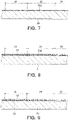
- Fig. 3 is a partial plan view of the vapor deposition mask device 10 as viewed from the first face 20a side of the vapor deposition mask 20, and is an enlarged view of the portion enclosed by the dashed-dotted line marked by reference sign III in Fig. 1 .
- Fig. 4 is a diagram showing the vapor deposition mask device 10 in a cross section taken along line IV-IV in Fig. 3 .
- Fig. 5 is a partial plan view of a vapor deposition mask 20 of the vapor deposition mask device 10 of Fig. 3 , and is an enlarged view of the portion enclosed by the dashed-dotted line marked by reference sign V in Fig.
- Fig. 6 is a diagram showing a vapor deposition mask 20 in a cross section taken along line VI-VI in Fig. 5 .
- the first metal layer 32 to be described later is, in detail, at least part of the face on a second face 20b side exposed from the second metal layer 37 is formed as a curved face.
- the cross section of the first metal layer 32 is shown as a simple rectangle in order to avoid complication of the drawing. The same applies to Figs. 11 to 18 , 20 and 25 .
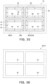
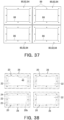
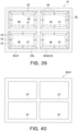
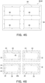
- the vapor deposition mask 20 has a substantially quadrilateral shape in plan view, and more precisely, a substantially rectangular outline in plan view.
- the vapor deposition mask 20 has the effective region 22 in which the first through holes 25 are formed in a regular arrangement, a peripheral region 23 surrounding the effective region 22, and the ear region 24 located at the periphery of the vapor deposition mask 20.
- the vapor deposition mask 20 has a plurality of effective regions 22, and the plurality of effective regions 22 is arranged at predetermined pitches along the two directions orthogonal to each other.
- one effective region 22 corresponds to one organic EL display device. That is, according to the illustrated vapor deposition mask device 10, the multifaceted vapor deposition on the substrate to be vapor-deposited is possible.
- the ear region 24 is located to surround the peripheral region 23 and forms an outer edge 26 of the vapor deposition mask 20.
- the peripheral region 23 is a region for supporting the effective region 22, and the ear region 24 is a region for attaching the vapor deposition mask 20 to the frame 15. Therefore, neither the peripheral region 23 nor the ear region 24 is a region through which the vapor deposition material 98 intended to be deposited on the organic EL substrate 92 passes.
- the effective region 22 is a region in the vapor deposition mask 20 facing a zone to be a display region of the organic EL substrate 92 where the organic light emitting material is vapor deposited to form a pixel. In the example shown in Fig.
- each effective region 22 has a substantially quadrilateral shape in plan view, and more precisely, a substantially rectangular outline in plan view.
- the effective region 22 has a thickness T 1 (see Fig. 4 ), and the thickness T 1 is, for example, 2 ⁇ m or more and 50 ⁇ m or less.
- each effective region 22 can have outlines of various shapes according to the shape of the display region of the organic EL substrate 92.
- each effective region 22 may have a circular outline.
- the vapor deposition mask device 10 has a plurality of joint portions 60 that joins the vapor deposition mask 20 and the frame 15 to each other.
- the plurality of joint portions 60 is arranged along the outer edge 26 in the ear region 24 of the vapor deposition mask 20.
- the vapor deposition mask 20 has a substantially rectangular outline in plan view. Therefore, the plurality of joint portions 60 is also arranged in a substantially rectangular pattern along the outer edge 26 of the vapor deposition mask 20. In the example shown in Fig. 3 , the plurality of joint portions 60 is arranged in a straight line with a certain distance from the outer edge 26 of the vapor deposition mask 20.
- the plurality of joint portions 60 is arranged along a direction parallel to the direction in which the outer edge 26 of the vapor deposition mask 20 extends. In the illustrated example, the plurality of joint portions 60 is arranged at equal intervals along the direction in which the outer edge 26 extends.
- the vapor deposition mask 20 and the frame 15 are fixed to each other by spot welding. Therefore, each joint portion 60 is configured as a weld portion by spot welding.
- the invention is not limited thereto, and the vapor deposition mask 20 and the frame 15 may be fixed to each other by another fixing means, such as an adhesive agent, for example. That is, each joint portion 60 may be configured as, for example, an adhesive portion.
- a notch 42 is formed at a position corresponding to between two adjacent joint portions 60 in the outer edge 26 of the vapor deposition mask 20.
- the position corresponding to between two adjacent joint portions 60 at the outer edge 26 of the vapor deposition mask 20 refers to a portion of the outer edge 26 located in a direction orthogonal to the direction connecting the two adjacent joint portions 60 in the plate face of the vapor deposition mask 20 from the position between two adjacent joint portions 60.
- the notch 42 is formed including the position corresponding to the center between the two adjacent joint portions 60 in the outer edge 26 of the vapor deposition mask 20. That is, the notch 42 is formed including a portion of the outer edge 26 located in a direction orthogonal to the direction connecting the two adjacent joint portions 60 in the plate face of the vapor deposition mask 20 from the central position between two adjacent joint portions 60.
- etching solution can be made to permeate through the notch 42 from the outer edge 26 side of the vapor deposition mask 20 in the separation step described later, so that a conductive pattern 52 located between the frame 15 and a base material 51 can be easily etched away.
- Each notch 42 extends from the outer edge 26 of the vapor deposition mask 20 toward the effective region 22 in plan view.
- the notch 42 extends from the outer edge 26 of the vapor deposition mask 20 toward the effective region 22 with a certain width.
- the notch 42 extends from the ear region 24 over the peripheral region 23 of the vapor deposition mask 20.
- the invention is not limited thereto, and the notch 42 may be located only in the ear region 24 of the vapor deposition mask 20.
- the corner of the end of the notch 42 on the effective region 22 side is rounded.
- the end of the notch 42 on the effective region 22 side has a substantially semicircular shape.
- the vapor deposition mask 20 has a plurality of notches 42.
- the vapor deposition mask 20 has a polygonal shape in plan view, and a plurality of notches 42 is formed along one side of the polygon.
- the conductive pattern 52 located between the frame 15 and the base material 51 can be etched away more efficiently.
- the plurality of notches 42 has the same shape and size as one another in the illustrated example. However, the invention is not limited thereto, and the plurality of notches 42 may include two notches 42 having different shapes and/or sizes. For example, two notches 42 among the plurality of notches 42 may have different shapes and/or dimensions with each other in plan view of the vapor deposition mask 20. When the plurality of notches 42 includes two notches 42 having different shapes and/or dimensions with each other in plan view of the vapor deposition mask 20, the amount and/or rate of permeation of the etching solution to a space between the frame 15 and the base material 51 in the separation step can be locally changed in the two notches 42 concerned.
- the invention is not limited thereto, and it is also possible to intentionally make a local difference in the progress rate of etching removal of the conductive pattern 52 located between the frame 15 and the base material 51.
- the notch 42 extends beyond an inner edge 17 of the frame 15 in plan view.
- a gap 18 is formed between the end of the notch 42 on the effective region 22 side and the inner edge 17 of the frame 15.
- the etching solution can be made to permeate through the gap 18 from the inner edge 17 side of the frame 15, so that the conductive pattern 52 located between the frame 15 and the base material 51 can be etched away more easily.
- a joint piece 44 is formed between two adjacent notches 42. In other words, the joint piece 44 is located between the two adjacent notches 42.
- the vapor deposition mask 20 is joined to the frame 15 at the joint piece 44. That is, the joint piece 44 and the frame 15 are fixed to each other via the joint portion 60.
- one joint portion 60 is disposed on one joint piece 44.
- a plurality of joint pieces 44 is arranged along the outer edge 26 of the vapor deposition mask 20. The plurality of joint pieces 44 is arranged at equal intervals along the direction in which the outer edge 26 extends.
- Each joint piece 44 extends from the outer edge 26 of the vapor deposition mask 20 toward the effective region 22 in plan view. In the example shown in Fig. 3 , the joint piece 44 extends from the outer edge 26 of the vapor deposition mask 20 toward the effective region 22 with a certain width except for a partial region on the effective region 22 side. In the illustrated example, the joint piece 44 extends from the ear region 24 of the vapor deposition mask 20 over the peripheral region 23. In addition, the invention is not limited thereto, and the joint piece 44 may be located only in the ear region 24 of the vapor deposition mask 20.
- each joint piece 44 is disposed at the outermost periphery of the vapor deposition mask 20.
- An end 45 located opposite the effective region 22 along the direction in which each joint piece 44 extends constitutes part of the outer edge 26 of the vapor deposition mask 20. Therefore, in the present embodiment, a substantially rectangular virtual line formed by connecting each end 45 of the plurality of joint pieces 44 forms the outer edge 26 of the vapor deposition mask 20.
- the notch 42 has a first width W 1 along the direction in which the outer edge extends.
- the joint piece 44 has a second width W 2 along the direction in which the outer edge 26 extends.
- the first width W 1 of the notch 42 is larger than the second width W 2 of the joint piece 44.
- the first width W 1 of the notch 42 can be, for example, 1 mm or more and 10 mm or less.
- the second width W 2 of the joint piece 44 can be, for example, 1 mm or more and 3 mm or less.
- the length L of the joint piece 44 (the length of the notch 42) can be, for example, 0.5 mm or more and 2.5 mm or less.
- the vapor deposition mask 20 includes the first metal layer 32, the second metal layer 37 and the ear metal layer 38.
- the first metal layer 32, the second metal layer 37 and the ear metal layer 38 are collectively referred to simply as a metal layer.
- the first metal layer 32 is disposed on the first face 20a side of the vapor deposition mask 20.
- the second metal layer 37 is disposed closer to the second face 20b of the vapor deposition mask 20 than the first metal layer 32.
- the ear metal layer 38 is disposed between the first metal layer 32 and the second metal layer 37 in the ear region 24 of the vapor deposition mask 20.
- a face of the first metal layer 32 opposite the second metal layer 37 constitutes the first face 20a of the vapor deposition mask 20
- a face of the second metal layer 37 opposite the first metal layer 32 constitutes the second face 20b of the vapor deposition mask 20.
- the illustrated ear region 24 of the vapor deposition mask 20 has a thickness larger than that of the effective region 22 since it has the ear metal layer 38. That is, the thickness T 2 of the ear region 24 of the vapor deposition mask 20 is larger than the thickness T 1 of the effective region 22.
- the thickness T 2 of the ear region 24 can be, for example, 15 ⁇ m or more and 50 ⁇ m or less.
- the thickness of the ear metal layer 38 can be, for example, 10 ⁇ m or more and 45 ⁇ m or less.
- the relatively thickly formed ear region 24 can support the thinned effective region 22, so that it is possible to suppress deformation in the effective region 22, and improve handling of the vapor deposition mask 20.
- the vapor deposition mask 20 is manufactured using a plating method.
- residual stress internal stress
- This residual stress tends to increase at a so-called solid portion in the metal layer.
- the solid portion refers to a region in the metal layer where the opening is not formed.
- the residual stress generated in the metal layer also increases. Therefore, in the vapor deposition mask 20 of the present embodiment, the relatively large residual stress can occur in the ear region 24 having a large thickness compared to the effective region 22.
- the first width W 1 of the notch 42 is larger than the second width W 2 of the joint piece 44.
- the area of the solid portion in the ear region 24 having a large thickness is reduced, so that the residual stress generated in the ear region 24 can be reduced. Therefore, the deformation of the effective region 22 can be suppressed, and the dimensional accuracy and positional accuracy of the vapor deposition material vapor-deposited through the vapor deposition mask 20 can be improved.
- each joint portion 60 close to the inner edge 17 of the frame 15, that is, to reduce the distance D between the joint portion 60 and the inner edge 17 of the frame 15.
- the distance D is, in the plate face of the vapor deposition mask 20, the distance between the joint portion 60 and the inner edge 17 of the frame 15 measured in the direction orthogonal to the arrangement direction of the plurality of joint portions 60.
- the distance D can be, for example, 0.5 mm or more and 2.5 mm or less.
- the plurality of first through holes 25 formed in each effective region 22 will be described.
- the plurality of first through holes 25 formed in the effective region 22 is arranged at predetermined pitches along two directions orthogonal to each other in the effective region 22.
- the shape and the like of the first through holes 25 when the vapor deposition mask 20 is formed by plating treatment will be described.
- the vapor deposition mask 20 includes the first metal layer 32 having a first opening 30 in a predetermined pattern, and the second metal layer 37 having a second opening 35 communicating with the first opening 30 in each effective region 22.
- the first through hole 25 penetrating the vapor deposition mask 20 is composed of the first opening 30 and the second opening 35 communicating with each other.
- the opening size and the opening shape of the first through hole 25 on the first face 20a side of the vapor deposition mask 20 are defined by the first opening 30 of the first metal layer 32.
- the opening size and the opening shape of the first through hole 25 on the second face 20b side of the vapor deposition mask 20 are defined by the second opening 35 of the second metal layer 37.
- the first through holes 25 has both the shape defined by the first opening 30 of the first metal layer 32 and the shape defined by the second opening 35 of the second metal layer 37.
- the first opening 30 and the second opening 35 constituting the first through hole 25 may have a substantially polygonal shape in plan view.
- the first opening 30 and the second opening 35 have a substantially quadrilateral shape, more specifically, a substantially square shape.
- the first opening 30 and the second opening 35 may have another substantially polygonal shape such as a substantially hexagonal shape or a substantially octagonal shape.
- the "substantially polygonal shape” is a concept including a shape in which the corner of a polygon is rounded.
- the first opening 30 and the second opening 35 may have a circular shape, an elliptical shape, or the like. As long as the second opening 35 has an outline surrounding the first opening 30 in plan view, the shape of the first opening 30 and the shape of the second opening 35 do not have to be similar.
- reference sign 41 represents a connection portion to which the first metal layer 32 and the second metal layer 37 are connected. Further, reference sign S0 represents the dimension of the first through hole 25 in the connection portion 41 between the first metal layer 32 and the second metal layer 37.
- reference sign S0 represents the dimension of the first through hole 25 in the connection portion 41 between the first metal layer 32 and the second metal layer 37.
- the present invention is no limitation thereto, and another layer may be interposed between the first metal layer 32 and the second metal layer 37.
- a catalyst layer for promoting the deposition of the second metal layer 37 on the first metal layer 32 may be provided between the first metal layer 32 and the second metal layer 37.
- the opening dimension S2 of the first through hole 25 (second opening 35) in the second face 20b is larger than the opening dimension S1 of the first through hole 25 (first opening 30) in the first face 20a.
- a path with the smallest angle with respect to the normal direction N of the vapor deposition mask 20 of the paths of the vapor deposition material 98 that pass through an end 36 of the first through hole 25 (second opening 35) on the second face 20b side of the vapor deposition mask 20 and which can reach the organic EL substrate 92 is represented by reference sign L1.
- An angle between the path L1 and the normal direction N of the vapor deposition mask 20 is represented by reference sign ⁇ 1.
- the angle ⁇ 1 is preferably 45° or more.
- the above-described opening dimensions S0, S1, and S2 are appropriately set in consideration of the pixel density of the organic EL display device, the desired value of the above-mentioned angle ⁇ 1, and the like.
- the opening dimension S0 of the first through hole 25 in the connection portion 41 can be set in the range of 15 ⁇ m to 60 ⁇ m.
- the opening dimension S1 of the first opening 30 in the first face 20a is set in the range of 10 ⁇ m to 50 ⁇ m
- the opening dimension S2 of the second opening 35 in the second face 20b can be set in the range of 15 ⁇ m to 60 ⁇ m.
- the total thickness T 1 of the first metal layer 32 and the second metal layer 37 in the effective region 22 can be, for example, 2 ⁇ m to 50 ⁇ m.
- the thickness T 1 of the vapor deposition mask 20 in the effective region 22 has such a thickness, the vapor deposition mask 20 is sufficiently thinned while having desired durability, so that it is possible to suppress inhibition of the adhesion, to the organic EL substrate 92, of the vapor deposition material directed to the organic EL substrate 92 from the oblique direction, that is, the direction inclined with respect to both the direction of the plate face of the organic EL substrate 92 and the normal direction to the plate face, that is, to suppress inhibition of the occurrence of adhesion unevenness of the organic material.
- the oblique direction that is, the direction inclined with respect to both the direction of the plate face of the organic EL substrate 92 and the normal direction to the plate face
- An iron alloy containing nickel can be used as a main material of the first metal layer 32, the second metal layer 37 and the ear metal layer 38.
- an invar material containing 34 mass% or more and 38 mass% or less of nickel, and an iron alloy such as a super-invar material further containing cobalt in addition to nickel can be used.
- the invention is not limited thereto, and as a main material of the first metal layer 32 and the second metal layer 37, for example, iron alloys other than iron alloys containing nickel described above, such as iron alloys containing chromium, may be used.
- an iron alloy containing chromium for example, an iron alloy referred to as a so-called stainless steel can be used. Alloys such as nickel and nickel-cobalt alloys, which are other than iron alloys, may be used.
- the first metal layer 32 and the second metal layer 37 may be composed of materials having the same composition, or may be composed of materials having different compositions.
- the vapor deposition mask 20 has, between the plurality of joint portions 60 and the effective region 22, a plurality of third through holes 48 which does not overlap the frame 15 in plan view.
- the plurality of third through holes 48 is provided in the peripheral region 23 of the vapor deposition mask 20.
- the third through hole 48 is intended to allow the etching solution to permeate through the third through holes 48 in the separation step described later.
- the third through hole 48 has a circular shape in plan view.
- the third through holes 48 are formed to have the same shape and dimensions as one another. However, the invention is not limited thereto, and the third through holes 48 may be formed to have different shapes or dimensions.
- the diameter of the third through hole 48 can be, for example, 20 ⁇ m or more and 50 ⁇ m or less.
- the etching solution can be made to permeate through the third through holes 48 in the separation step described later, so that the conductive pattern 52 located between the plurality of joint portions 60 and the effective region 22, particularly in the peripheral region 23, can be easily etched away.
- the base material 51 is prepared.
- the material of the base material 51 or the thickness of the base material 51 as long as the base material 51 has insulating properties and an appropriate strength.
- a glass material having high light transparency may be suitably used as a material of the base material 51.
- the base material 51 may not have light transparency.
- a conductive layer 52a made of a conductive material is formed.
- the conductive layer 52a is a layer to be the conductive pattern 52 by being patterned.
- a metal material or a material which has electroconductivity, such as an oxide conductive material, is appropriately used as a material of the conductive layer 52a.
- a metal material include, for example, chromium, copper, and the like.
- a material having high adhesion to a first resist pattern 53 described later is used as a material of the conductive layer 52a.
- the first resist pattern 53 is formed by patterning a so-called dry film such as a resist film containing an acrylic photocurable resin, preferably, copper is used as a material of the conductive layer 52a.
- the conductive layer 52a is formed by, for example, sputtering or electroless plating.
- the conductive layer 52a When the conductive layer 52a is to be formed thick, it takes a long time to form the conductive layer 52a.
- the thickness of the conductive layer 52a is preferably in the range of 50 nm to 500 nm.
- the first resist pattern 53 having a predetermined pattern is formed on the conductive layer 52a.
- a photolithography method or the like may be employed as a method of forming the first resist pattern 53.
- a method of irradiating the material for the first resist pattern 53 with light in a predetermined pattern a method in which the exposure mask that transmits exposure light in a predetermined pattern is used, and a method in which the material for the first resist pattern 53 is relatively scanned by exposure light in a predetermined pattern and the like may be employed.
- the portion of the conductive layer 52a not covered by the first resist pattern 53 is removed by etching.
- the first resist pattern 53 is removed.
- the first film forming process of manufacturing the above-described first metal layer 32 using the patterned substrate 50 will be described.
- the first metal layer 32 in which the first openings 30 are provided in a predetermined pattern is formed on the insulating base material 51.
- a first plating solution is supplied on the base material 51 on which the conductive pattern 52 is formed to perform a first plating treatment process of depositing the first metal layer 32 on the conductive pattern 52.
- the base material 51 on which the conductive pattern 52 is formed is immersed in a plating tank filled with the first plating solution.
- Fig. 11 it is possible to obtain the first metal layer 32, on the base material 51, in which the first openings 30 are provided in a predetermined pattern.
- the thickness of the first metal layer 32 is, for example, 5 ⁇ m or less. Note that forming the first metal layer 32 on the base material 51 is not limited to forming the first metal layer 32 directly on the base material 51, but also includes forming the first metal layer 32 via another layer such as the conductive pattern 52 on the base material 51.
- the specific method of the first plating treatment process is not particularly limited.
- the first plating treatment process may be performed as a so-called electrolytic plating treatment process in which the first metal layer 32 is deposited on the conductive pattern 52 by supplying a current to the conductive pattern 52.
- the first plating treatment process may be an electroless plating treatment process.
- an appropriate catalyst layer may be provided on the conductive pattern 52.
- the conductive pattern 52 may be configured to function as a catalyst layer. The catalyst layer may be provided on the conductive pattern 52 when the electrolytic plating treatment process is performed.
- the components of the first plating solution to be used are appropriately determined according to the characteristics required for the first metal layer 32.
- a mixed solution of a solution containing a nickel compound and a solution containing an iron compound can be used as the first plating solution.
- a mixed solution of a solution containing nickel sulfamate or nickel bromide and a solution containing ferrous sulfamate can be used.
- the plating solution may contain various additives.
- pH buffers such as boric acid, a primary brightener such as sodium saccharin, butynediol, propargyl alcohol, coumarin, formalin, a secondary brightener such as thiourea, an antioxidant, etc. may be used.
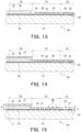
- Fig. 12 is a cross-sectional view of a second resist pattern 55 formed on the base material 51.
- the resist formation process is performed such that the first opening 30 of the first metal layer 32 is covered by the second resist pattern 55, and the gap 56 of the second resist pattern 55 is located on the first metal layer 32.
- the second resist pattern 55 is not formed in the region corresponding to the ear region 24.
- the gap 56 indicates a portion where the second resist pattern 55 is not formed. Therefore, it can be said that the gap 56 is formed also in the region corresponding to the ear region 24 of the vapor deposition mask 20.
- a negative resist film is formed by attaching a dry film on the base material 51 and the first metal layer 32.
- An example of a dry film includes, for example, a film which contains acrylic photocurable resin, such as RY3310 made by Hitachi Chemical Co., Ltd.
- a material for the second resist pattern 55 may be applied to the base material 51, and then, if necessary, firing may be performed to form a resist film.
- an exposure mask that prevents light from passing through the region to be the gap 56 of the resist film is prepared to place an exposure mask on the resist film. Thereafter, the exposure mask sufficiently comes into close contact with the resist film by vacuum contact.
- a positive type may be used as the resist film. In this case, as the exposure mask, an exposure mask which allows light to pass through a region to be removed of the resist film is used.
- the resist film is exposed through the exposure mask. Further, the resist film is developed to form an image on the exposed resist film.
- a heat treatment process of heating the second resist pattern 55 may be performed after the development process.
- the ear metal layer forming process of forming the ear metal layer 38 in the region corresponding to the ear region 24 is performed.
- a plating solution for forming the ear metal layer is supplied on the first metal layer 32 exposed from the shielding member to deposit the ear metal layer 38 on the first metal layer 32.
- the laminate of the base material 51, the conductive pattern 52, the first metal layer 32, and the second resist pattern 55 is immersed in a plating tank filled with a plating solution for forming the ear metal layer.
- the ear metal layer 38 can be formed on the first metal layer 32 in the ear region 24.
- the thickness of the ear metal layer 38 can be, for example, 10 ⁇ m or more and 45 ⁇ m or less.
- the specific method of the ear metal layer forming process is not particularly limited.
- the ear metal layer forming process may be performed as a so-called electrolytic plating treatment process in which the ear metal layer 38 is deposited on the first metal layer 32 by supplying a current to the first metal layer 32.
- the ear metal layer forming process may be an electroless plating treatment process.
- an appropriate catalyst layer may be provided on the first metal layer 32. The catalyst layer may be provided on the first metal layer 32 when the electrolytic plating treatment process is performed.
- the same plating solution as the above-described first plating solution may be used as the plating solution for forming the ear metal layer.
- a plating solution different from the first plating solution may be used as the plating solution for forming the ear metal layer.
- the composition of the first plating solution and the composition of the plating solution for forming the ear metal layer are the same, the composition of the metal of which the first metal layer 32 is made and the composition of the metal of which the ear metal layer 38 is made is also the same.
- the second film forming process of forming the second metal layer 37 on the first metal layer 32 and the ear metal layer 38 is performed.
- the second metal layer 37 having the second opening 35 communicating with the first opening 30 is formed on the first metal layer 32.
- the second metal layer 37 is formed over the first metal layer 32 and the ear metal layer 38.
- a second plating solution is supplied into the gap 56 of the second resist pattern 55 and on the ear metal layer 38 to perform a second plating treatment process of depositing the second metal layer 37 on the first metal layer 32 and the ear metal layer 38.
- the base material 51 on which the first metal layer 32 and the ear metal layer 38 are formed is immersed in a plating tank filled with the second plating solution.
- the second metal layer 37 can be formed on the first metal layer 32 and the ear metal layer 38.
- the thickness of the second metal layer 37 is set such that the thickness T 1 of the metal layer of the vapor deposition mask 20 in the effective region 22 is 2 ⁇ m or more and 50 ⁇ m or less.
- the thickness of the first metal layer 32 in the effective region 22 and the thickness of the first metal layer 32 in the ear region 24 are the same.
- the thickness of the second metal layer 37 in the effective region 22 and the thickness of the second metal layer 37 in the ear region 24 are also the same.
- the thickness T 2 of the ear region 24 is greater than the thickness T 1 of the effective region 22 due to the presence of the ear metal layer 38.
- the specific method of the second plating treatment process is not particularly limited.
- the second plating treatment process may be performed as a so-called electrolytic plating treatment process in which the second metal layer 37 is deposited on the first metal layer 32 and the ear metal layer 38 by applying a current to the first metal layer 32 and the ear metal layer 38.
- the second plating treatment process may be an electroless plating treatment process.
- an appropriate catalyst layer may be provided on the first metal layer 32 and the ear metal layer 38.
- a catalyst layer may be provided on the first metal layer 32 and the ear metal layer 38.
- the same plating solution as the first plating solution described above or the plating solution for forming the ear metal layer may be used as the second plating solution.
- a plating solution different from the first plating solution or the plating solution for forming the ear metal layer may be used as the second plating solution.
- composition of the plating solution for forming the ear metal layer and the composition of the second plating solution are the same, the composition of the metal of which the ear metal layer 38 is made and the composition of the metal of which the second metal layer 37 is made are also the same.
- Fig. 14 the example shows that the second plating treatment process is continued until the upper face of the second resist pattern 55 and the upper face of the second metal layer 37 are aligned.
- the present invention is not limited thereto.
- the second plating treatment process may be stopped with the upper face of the second metal layer 37 located below the upper face of the second resist pattern 55.
- a removal process of removing the second resist pattern 55 is performed.
- the removal process is performed by immersing a laminate of the patterned substrate 50, the first metal layer 32, the ear metal layer 38, the second metal layer 37, and the second resist pattern 55 in, for example, an alkaline stripping solution.
- an alkaline stripping solution As a result, as shown in Fig. 15 , the second resist pattern 55 can be separated from the patterned substrate 50, the first metal layer 32 and the second metal layer 37.
- a cutting process of cutting the patterned substrate 50, the first metal layer 32, the ear metal layer 38, and the second metal layer 37 along a cutting line at a position to be the outer edge 26 of the vapor deposition mask 20 is performed.
- this cutting line is indicated by the dashed-dotted line marked by reference sign C.
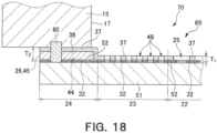
- a laminate 65 of the base material 51, the conductive pattern 52, the first metal layer 32, the ear metal layer 38, and the second metal layer 37 which is cut out is shown in Fig. 16 .
- a joining step of joining the metal layers (the first metal layer 32, the second metal layer 37, and the ear metal layer 38) to the frame 15 is performed.
- the metal layers of the laminate 65 including the base material 51, the conductive pattern 52 provided on the base material 51, and the metal layer provided on opposite side, with respect to the base material 51, of the conductive pattern 52 are joined to the frame 15 at a plurality of joint portions 60.
- the joint piece 44 in the laminate 65 is joined to the frame 15 (see Fig. 19 ).
- the metal layer and the frame 15 are fixed to each other by spot welding.
- the metal layer and the frame 15 are fixed to each other by laser spot welding.
- the invention is not limited thereto, and in a joining step, the metal layer and the frame 15 may be fixed to each other by, for example, another fixing means such as an adhesive.
- the laminate 65 and the frame 15 are disposed such that the second metal layer 37 of the joint piece 44 and the frame 15 are in contact with each other.
- the joint piece 44 of the laminate 65 is irradiated with the laser light La through the base material 51 from the base material 51 side to melt part of the joint piece 44 and part of the frame 15 by the heat generated by the irradiation with the laser light La, and the joint piece 44 and the frame 15 are fixed by welding.
- the laser light La for example, YAG laser light generated by a YAG laser device can be used.
- a YAG laser device it is possible to use a device provided with, for example, a crystal obtained by adding Nd (neodymium) to YAG (yttrium aluminum garnet) as a medium for oscillation.
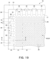
- Fig. 19 is a partial plan view of the intermediate member 70. In Fig. 19 , the intermediate member 70 is shown as viewed from the base material 51 side.
- the intermediate member 70 has a plurality of joint portions 60 that joins the metal layers 32, 37, and 38 of the laminate 65 (vapor deposition mask 20) and the frame 15 to each other, the plurality of joint portions 60 is arranged along the outer edge 26 of the laminate 65, and the notch 42 is formed at a position corresponding to between two adjacent joint portions 60 in the outer edge 26 of the laminate 65.
- a separation step of separating the combination of the first metal layer 32, the ear metal layer 38, the second metal layer 37 and the frame 15 from the base material 51 is performed.
- the intermediate member 70 is immersed in an etching solution capable of selectively etching the conductive pattern 52.
- the combination of the first metal layer 32, the ear metal layer 38, the second metal layer 37, and the frame 15 is peeled off and separated from the base material 51.
- the combination of the first metal layer 32, the ear metal layer 38, the second metal layer 37, and the frame 15 is immersed again in the etching solution to completely etch away the conductive pattern 52 attached to and remaining on the first metal layer 32.
- the vapor deposition mask device 10 can be obtained in which the vapor deposition mask 20 including the first metal layer 32 having the first openings 30 in a predetermined pattern, the second metal layer 37 having the second opening 35 communicating with the first opening 30, and the ear metal layer 38 disposed between the first metal layer 32 and the second metal layer 37 in the ear region 24, and the frame 15 are joined by a plurality of joint portions 60.
- Fig. 20 is a view showing the intermediate member 70 in a cross section taken along line XX-XX in Fig. 19 .
- Fig. 21 is a diagram showing the intermediate member 70 in a cross section taken along line XXI-XXI in Fig. 19 .
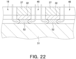
- Fig. 22 is an enlarged view of part of the cross section of Fig. 20 , and in particular, shows the intermediate member 70 in the region enclosed by the dashed-dotted line marked by reference sign XXII in Fig. 20 .
- the etching solution permeates into the notch 42 from the outer edge 26 side of the laminate 65 (vapor deposition mask 20). In the illustrated example, the etching solution also permeates into the notch 42 from the inner edge 17 side of the frame 15 via the gap 18.
- the conductive pattern 52 present between the joint piece 44 and the base material 51 is exposed in the notch 42. Therefore, by means of the etching solution that has permeated into the notch 42, the conductive pattern 52 is etched from the exposed face in the notch 42 or side face.
- an etching solution by using an etching solution that does not dissolve the first metal layer 32, the ear metal layer 38, the second metal layer 37, or the frame 15, but that dissolves only the conductive pattern 52, the first metal layer 32, the ear metal layer 38, the second metal layer 37, and the frame 15 are not eroded by the etching solution, and only the conductive pattern 52 can be dissolved and removed.
- the etching progresses inward from both side faces of the conductive pattern 52. As the etching progresses, a face formed by the etching progressing from one side and a face formed by the etching progressing from the other side are connected. As a result, the first metal layer 32 of the joint piece 44 and the base material 51 are separated.
- the vapor deposition mask 20 has a plurality of third through holes 48 provided between the plurality of joint portions 60 and the effective region 22 and not overlapping the frame 15 in plan view.
- the etching solution permeates into the third through holes 48.
- the conductive pattern 52 present between the first metal layer 32 and the base material 51 in the peripheral region 23 is exposed in the third through hole 48. Therefore, by means of the etching solution that has permeated into the third through hole 48, the conductive pattern 52 is etched from the exposed face in the third through hole 48 or side face. In the illustrated example, the etching progresses inward from both side faces of the conductive pattern 52. As the etching progresses, a face formed by the etching advanced from one side and a face formed by the etching progressed from the other side are connected. As a result, the first metal layer 32 in the peripheral region 23 and the base material 51 are separated.
- the conductive pattern 52 present between the first metal layer 32 and the base material 51 in the effective region 22 is exposed in the first through hole 25. Therefore, by means of the etching solution that has permeated into the first through holes 25, the conductive pattern 52 is etched from the exposed face or side face in the first through hole 25. In the illustrated example, the etching progresses inward from both side faces of the conductive pattern 52. As the etching progresses, a face formed by the etching advanced from one side and a face formed by the etching progressed from the other side are connected. As a result, the first metal layer 32 in the effective region 22 and the base material 51 are separated.
- the conductive pattern 52 is etched away from the intermediate member 70, and the first metal layer 32 and the base material 51 are separated. That is, the combination of the first metal layer 32, the ear metal layer 38, the second metal layer 37 and the frame 15 is separated from the base material 51.
- the first metal layer 32 and the base material 51 may not be completely separated. That is, the first metal layer 32 and the base material 51 may be partially connected by the conductive pattern 52.
- the conductive pattern 52 partially connecting the first metal layer 32 and the base material 51 is broken, and the base material 51 can be separated from the combination.
- the conductive pattern 52 attached to and remaining on the first metal layer 32 can be completely etched away by immersing the combination of the first metal layer 32, the ear metal layer 38, the second metal layer 37, and the frame 15 in the etching solution again.
- a vapor deposition mask device 10 includes the vapor deposition mask 20 having the effective region 22 in which a plurality of first through holes 25 is disposed, and the frame 15 attached to the vapor deposition mask 20, wherein the vapor deposition mask device 10 includes a plurality of joint portions 60 that joins the vapor deposition mask 20 and the frame 15 to each other, the plurality of joint portions 60 is arranged along the outer edge 26 of the vapor deposition mask 20, and the notch 42 is formed at a position corresponding to between two adjacent joint portions 60 in the outer edge 26 of the vapor deposition mask 20.
- the etching solution can be made to permeate through the notch 42 from the outer edge 26 side of the laminate 65 (vapor deposition mask 20), so that the conductive pattern 52 located between the frame 15 and the base material 51, that is, between the joint piece 44 and the base material 51, can be easily etched away.
- the vapor deposition mask 20 can be joined to the frame 15, so that wrinkles and deformation of the vapor deposition mask 20 of the vapor deposition mask device 10 can be effectively suppressed.
- the vapor deposition mask 20 includes the joint piece 44 located between two adjacent notches 42, wherein at the outer edge 26, the notch 42 has the first width W 1 along the direction in which the outer edge 26 extends, the joint piece 44 has the second width W 2 along the direction in which the outer edge 26 extends, and the first width W 1 is larger than the second width W 2 .
- the etching solution in the separation step can be made to permeate through the notch 42 having a first width W 1 larger than the second width W 2 of the joint piece 44 from the outer edge 26 side of the laminate 65 (the vapor deposition mask 20), so that the conductive pattern 52 located between the frame 15 and the base material 51, that is, between the joint piece 44 and the base material 51, can be etched away more easily. Therefore, separation of the base material 51 from the combination of the metal layers 32, 37, and 38 and the frame 15 can be performed in a short time, and the manufacture of the vapor deposition mask device 10 can be effectively speeded up.
- the area of the solid portion in the ear region 24 having a large thickness as compared with the effective region 22 is reduced, and the metal layers 32, 37, and 38 are formed by using a plating method, so that it is possible to reduce the residual stress (internal stress) generated in the ear region 24. Therefore, the deformation of the effective region 22 can be suppressed, and the dimensional accuracy and positional accuracy of the vapor deposition material vapor-deposited through the vapor deposition mask 20 can be improved.
- the notch 42 extends beyond the inner edge 17 of the frame 15 in plan view of the vapor deposition mask 20.
- the gap 18 can be formed between the end of the notch 42 on the effective region 22 side and the inner edge 17 of the frame 15.
- the etching solution can be made to permeate through the gap 18 from the inner edge 17 side of the frame 15, so that the conductive pattern 52 located between the frame 15 and the base material 51 can be etched away more easily.
- the vapor deposition mask 20 has a polygonal shape in plan view, and a plurality of notches 42 is formed along one side of the polygon.
- a plurality of notches 42 is formed on one side of the polygon that constitutes the plan view shape of the vapor deposition mask 20, so that the conductive pattern 52 located between the frame 15 and the base material 51 can be etched away more efficiently.
- the vapor deposition mask device 10 of the present embodiment includes a plurality of notches 42, wherein the plurality of notches 42 includes two notches 42 having shapes and/or dimensions different from each other in plan view of the vapor deposition mask 20.
- the vapor deposition mask device 10 includes two notches 42 having different shapes and/or dimensions with each other, so that the amount and/or rate of permeation of the etching solution to a space between the frame 15 and the base material 51 in the separation step can be locally changed in the two notches 42 concerned. As a result, it is possible to make uniform the progress rate of etching removal of the conductive pattern 52 located between the frame 15 and the base material 51.
- the invention is not limited thereto, and it is also possible to intentionally make a local difference in the progress rate of etching removal of the conductive pattern 52 located between the frame 15 and the base material 51.
- the vapor deposition mask 20 has, between the plurality of joint portions 60 and the effective region 22, a plurality of third through holes 48 which does not overlap the frame 15 in plan view.
- the etching solution can be made to permeate through the third through holes 48 in the separation step, so that the conductive pattern 52 located between the plurality of joint portions 60 and the effective region 22, particularly in the peripheral region 23, can be easily etched away. Therefore, separation of the base material 51 from the combination of the metal layers 32, 37, and 38 and the frame 15 can be performed in a shorter time, and the manufacture of the vapor deposition mask device 10 can be effectively speeded up.
- the method of manufacturing the vapor deposition mask device 10 is a method of manufacturing the vapor deposition mask device 10 which includes the vapor deposition mask 20 having the effective region 22 in which the plurality of first through holes 25 is arranged, and the frame 15 attached to the vapor deposition mask 20.
- the method includes a joining step of joining, to the frame 15, the metal layers 32, 37, and 38 of the laminate 65 including the base material 51, the conductive pattern 52 provided on the base material 51, and the metal layers 32, 37, and 38 provided on opposite side, with respect to the base material 51, of the conductive pattern 52 by the plurality of joint portions 60, and a separation step of etching away the conductive pattern 52 to separate the base material 51 from the metal layers 32, 37, and 38, and forming the vapor deposition mask 20 from the metal layers 32, 37, and 38.
- the metal layers 32, 37, and 38 of the laminate 65 forming the vapor deposition mask 20 can be joined to the frame 15 while being held on the base material 51, so that even while joining the vapor deposition mask 20 to the frame 15 without applying tension to the vapor deposition mask 20, the flatness of the vapor deposition mask 20 can be secured.
- a plurality of joint portions 60 is arranged along the outer edge 26 of the metal layers 32, 37, and 38, and the notch 42 is formed, in the outer edge 26 of the metal layers 32, 37, and 38, at a position corresponding to between two adjacent joint portions 60 in the arrangement direction of the plurality of joint portions 60.
- the etching solution can be made to permeate through the notch 42 from the outer edge 26 side of the laminate 65 (the vapor deposition mask 20), so that the conductive pattern 52 located between the frame 15 and the base material 51, that is, between the joint piece 44 and the base material 51, can be etched away easily.
- Fig. 23 is a partial plan view of a modification of the vapor deposition mask device 10 described herein in general.
- the vapor deposition mask 20 of the vapor deposition mask device 10 has, between the plurality of joint portions 60 and the effective region 22, a plurality of second through holes 46 overlapping the inner edge 17 of the frame 15 in plan view.
- Each second through hole 46 is disposed at a position corresponding to between two adjacent joint portions 60.
- the fact that the second through hole 46 overlaps the inner edge 17 of the frame 15 in plan view, and is disposed at a position corresponding to between two adjacent joint portions 60 indicates that the second through hole 46 overlaps the portion of the inner edge 17 of the frame 15 located in the direction orthogonal to the direction connecting the two adjacent joint portions 60 in the plate face of the vapor deposition mask 20 from a position between the two adjacent joint portions 60.
- the second through hole 46 is formed including a position corresponding to the center between two adjacent joint portions 60 in the inner edge 17 of the frame 15.
- the second through hole 46 is formed including a portion of the inner edge 17 of the frame 15 located in a direction orthogonal to the direction connecting the two adjacent joint portions 60 in the plate face of the vapor deposition mask 20 from the central position between two adjacent joint portions 60.
- each second through hole 46 is formed in a circular shape in plan view.
- each second through hole 46 may have another shape such as an elliptical shape or a polygonal shape such as a rectangular shape in plan view.
- the corners are rounded from the viewpoint of alleviating stress concentration in the second through hole 46 when an external force acts on the vapor deposition mask 20.
- the diameter of the second through hole 46 can be, for example, 1 mm or more and 10 mm or less.
- the vapor deposition mask 20 has the gap 18 between the peripheral edge of the second through hole 46 on the effective region 22 side and the inner edge 17 of the frame 15.
- the etching solution can be made to permeate through the gap 18 formed by the second through holes 46 and the inner edge 17 of the frame 15 from the inner edge 17 side of the frame 15 in the separation step, so that the conductive pattern 52 located between the frame 15 and the base material 51 can be easily etched away.
- the second through hole 46 has a third width W 3 along the direction in which the inner edge 17 extends.
- the metal layer of the vapor deposition mask 20 located between the two adjacent second through holes 46 in the direction in which the inner edge 17 extends has a fourth width W 4 along the direction in which the inner edge 17 extends.
- the third width W 3 is larger than the fourth width W 4 .
- the third width W 3 is larger than the fourth width W 4 , the area of the solid portion in the ear region 24 having a large thickness as compared with the effective region 22 is reduced, and the metal layers 32, 37, and 38 are formed by using a plating method, so that it is possible to reduce the residual stress (internal stress) generated in the ear region 24. Therefore, the deformation of the effective region 22 can be suppressed, and the dimensional accuracy and positional accuracy of the vapor deposition material vapor-deposited through the vapor deposition mask 20 can be improved.
- the third width W 3 can be, for example, 1 mm or more and 10 mm or less.
- the fourth width W 4 can be, for example, 1 mm or more and 3 mm or less.
- the vapor deposition mask 20 may have only the second through hole 46 without the notch 42.
- the intermediate member 70 including the base material 51, the first metal layer 32, the ear metal layer 38, the second metal layer 37, and the frame 15 is obtained as shown in Fig. 24 .
- the intermediate member 70 is shown as viewed from the base material 51 side.
- the intermediate member 70 has a plurality of joint portions 60 that joins the metal layers 32, 37, and 38 of the laminate 65 (vapor deposition mask 20) and the frame 15 to each other, the plurality of joint portions 60 is arranged along the outer edge 26 of the laminate 65, the laminate 65 has, between the plurality of joint portions 60 and the effective region 22, a plurality of second through holes 46 overlapping the inner edge 17 of the frame 15 in plan view, and each second through hole 46 is disposed at a position corresponding to between two adjacent joint portions 60.
- Fig. 25 is a view of the intermediate member 70 in a cross section taken along line XXV-XXV in Fig. 24 .
- the etching solution permeates into the second through hole 46 through the gap 18 from the inner edge 17 side of the frame 15.
- the conductive pattern 52 located between the frame 15 and the base material 51 has a side face exposed in the second through hole 46. Therefore, the conductive pattern 52 is etched from the side face exposed to the second through hole 46 by means of the etching solution that has permeated into the second through hole 46. In the illustrated example, etching progresses inward from the side face of the conductive pattern 52 exposed to the second through hole 46.
- the etching solution permeates into the notch 42 also from the outer edge 26 side of the laminate 65 (vapor deposition mask 20).
- the conductive pattern 52 located between the frame 15 and the base material 51 also has a side face exposed in the notch 42. Therefore, the conductive pattern 52 is also etched from the side face exposed in the notch 42 by means of the etching solution that has permeated into the notch 42.
- the etching progresses inward from both side faces of the conductive pattern 52.
- a face formed by etching progressing from one side and a face formed by the etching progressing from the other side are connected.
- the first metal layer 32 located between the frame 15 and the base material 51 and the base material 51 are separated.
- the conductive pattern 52 present between the first metal layer 32 and the base material 51 in the peripheral region 23, and the conductive pattern 52 present between the first metal layer 32 and the base material 51 in the effective region 22 are etched away in the same manner as the above embodiment.
- the conductive pattern 52 is etched away from the intermediate member 70, and the first metal layer 32 and the base material 51 are separated. That is, the combination of the first metal layer 32, the ear metal layer 38, the second metal layer 37 and the frame 15 is separated from the base material 51.
- the vapor deposition mask device 10 includes the vapor deposition mask 20 having the effective region 22 in which a plurality of first through holes 25 is disposed, and the frame 15 attached to the vapor deposition mask 20, wherein the vapor deposition mask device 10 includes a plurality of joint portions 60 that joins the vapor deposition mask 20 and the frame 15 to each other, the plurality of joint portions 60 is arranged along the outer edge 26 of the vapor deposition mask 20, and the vapor deposition mask 20 has, between the plurality of joint portions 60 and the effective region 22, a plurality of second through holes 46 overlapping the inner edge 17 of the frame 15 in plan view, and each second through hole 46 is disposed at a position corresponding to between two adjacent joint portions 60.
- the etching solution can be made to permeate through the second through holes 46 from the inner edge 17 side of the frame 15, so that the conductive pattern 52 located between the frame 15 and the base material 51 can be easily etched away.
- the vapor deposition mask 20 can be joined to the frame 15, so that wrinkles and deformation of the vapor deposition mask 20 of the vapor deposition mask device 10 can be effectively suppressed.
- the second through hole 46 in the region overlapping the inner edge 17 of the frame 15 in plan view, has the third width W 3 along the direction in which the inner edge 17 extends, the metal layer of the vapor deposition mask 20 located between the two adjacent second through holes 46 in the direction in which the inner edge 17 extends has the fourth width W 4 along the direction in which the inner edge 17 extends, and the third width W 3 is larger than the fourth width W 4 .
- the etching solution can be made to permeate through the second through hole 46 having the third width W 3 larger than the fourth width W 4 from the inner edge 17 side of the frame 15 in the separation step, so that the conductive pattern 52 located between the frame 15 and the base material 51 can be etched away more easily. Therefore, separation of the base material 51 from the combination of the metal layers 32, 37, and 38 and the frame 15 can be performed in a short time, and the manufacture of the vapor deposition mask device 10 can be effectively speeded up.
- the area of the solid portion in the ear region 24 having a large thickness as compared with the effective region 22 is reduced, and the metal layers 32, 37, and 38 are formed by using a plating method, so that it is possible to reduce the residual stress (internal stress) generated in the ear region 24. Therefore, the deformation of the effective region 22 can be suppressed, and the dimensional accuracy and positional accuracy of the vapor deposition material vapor-deposited through the vapor deposition mask 20 can be improved.
- the plurality of joint portions 60 is arranged along the outer edge 26 of the metal layers 32, 37, and 38, the metal layers 32, 37, and 38 have, between the plurality of joint portions 60 and the effective region 22, a plurality of second through holes 46 overlapping the inner edge 17 of the frame 15 in plan view, and each second through hole 46 is disposed at a position corresponding to between two adjacent joint portions 60 in the arrangement direction of the plurality of joint portions 60.
- the etching solution can be made to permeate through the second through holes 46 from the inner edge 17 side of the frame 15 in the separation step, so that the conductive pattern 52 located between the frame 15 and the base material 51 can be easily etched away.
- Fig. 26 is a plan view of the vapor deposition mask device 10 according to the present modification
- Fig. 27 is an enlarged partial plan view of part of the vapor deposition mask device 10 in an enlarged manner, and is a diagram showing a portion enclosed by the dashed-dotted line marked by XXVII in Fig. 26
- Fig. 28 is a diagram showing the vapor deposition mask device 10 in a cross section taken along line XXVIII-XXVIII in Fig. 27
- Fig. 29 is a plan view of the vapor deposition mask 20 of the vapor deposition mask device 10
- Fig. 30 is a plan view of a frame 80 of the vapor deposition mask device 10.
- the vapor deposition mask device 10 shown in Fig. 26 includes a vapor deposition mask 20 having a substantially rectangular shape in plan view, and the frame 80 attached to the periphery of the vapor deposition mask 20.
- the vapor deposition mask device 10 has a plurality of vapor deposition masks 20.
- the plurality of vapor deposition masks 20 is arranged parallel to a plate face of a second frame 82, described later, of the frame 80 and along two directions crossing each other. Especially in the illustrated example, the plurality of vapor deposition masks 20 is arranged along two directions orthogonal to each other.
- Each vapor deposition mask 20 has one effective region 22.
- Each vapor deposition mask 20 corresponds to the display region of one organic EL display device.
- the multifaceted vapor deposition of the organic EL display device is possible corresponding to each vapor deposition mask 20.
- the vapor deposition mask 20 includes a metal layer 31 and the plurality of first through holes 25 formed in the metal layer 31.
- the thickness of the vapor deposition mask 20 can be 2.5 ⁇ m or more and 30 ⁇ m or less as an example.
- the frame 80 includes a first frame 81 and the second frame 82 attached to the first frame 81.
- the second frame 82 has a substantially rectangular shape in plan view, and more precisely, a substantially rectangular outline in plan view.
- the first frame 81 is formed in a substantially rectangular frame shape, and the second frame 82 is attached to the first frame 81 so that each side of the second frame 82 corresponds to each side of the first frame 81.
- the second frame 82 includes a plate member 84 and a plurality of openings 86 formed in the plate member 84.
- the plurality of openings 86 is arranged along two directions crossing each other. Especially in the illustrated example, the plurality of openings 86 is arranged along two directions orthogonal to each other.
- one vapor deposition mask 20 is attached corresponding to one opening 86 of the second frame 82.
- the thickness of the second frame 82 can be, for example, 50 ⁇ m or more and 500 ⁇ m or less.
- the opening 86 of the second frame 82 has, for example, a substantially quadrilateral shape in plan view, and more precisely, a substantially rectangular outline in plan view.
- each opening 86 can have outlines of various shapes corresponding to the shape of the display region of the substrate to be vapor-deposited (organic EL substrate) 92.
- each opening 86 may have a circular outline.
- Fig. 26 , Fig. 27 and Fig. 30 show that the respective openings 86 have the same plan view shape with each other, the openings 86 may have different opening shapes.
- the second frame 82 may have a plurality of openings 86 having shapes different from each other in plan view.
- the first through hole 25 of the vapor deposition mask 20 has a planar size smaller than a planar size of the opening 86 of the second frame 82.
- the fact that the first through hole 25 has the planar size smaller than the planar size of the opening 86 means that the size of the first through holes 25 is smaller than the size of the opening 86 in all directions along the plate face of the second frame 82 (the plate face of the vapor deposition mask 20).
- the outline defining the opening 86 surrounds the outline defining the first through hole 25 located in the opening 86 in plan view.
- the maximum dimension of the first through hole 25 in the planar direction can be, for example, 5 ⁇ m or more and 100 ⁇ m or less.
- the first through hole 25 may have a slit shape having a longitudinal direction and a width direction orthogonal to the longitudinal direction in plan view.
- the maximum width along the width direction of the first through hole 25 can be, for example, 5 ⁇ m or more and 100 ⁇ m or less.
- the vapor deposition mask device 10 includes a plurality of first joint portions 61 (joint portions 60) that joins the second frame 82 and the vapor deposition mask 20 to each other.
- the first frame 81 and the second frame 82 are fixed to each other. Therefore, the vapor deposition mask device 10 includes a plurality of second joint portions 62 that joins the first frame 81 and the second frame 82 to each other.
- each of the first joint portion 61 and the second joint portion 62 may be constituted as a weld portion by spot welding.
- a plurality of alignment marks 49 is provided in the vicinity of the outer periphery of the effective region 22 of the vapor deposition mask 20.
- a plurality of alignment marks 89 is provided in the vicinity of each opening 86 of the second frame 82.
- some (for example, two) alignment marks 89 are shared between the adjacent openings 86.
- the alignment marks 49 and 89 are used to align the relative position between the vapor deposition mask 20 and the second frame 82 at a predetermined position when attaching the vapor deposition mask 20 to the second frame 82.
- the specific shape of the alignment marks 49 and 89 may be any shape that can be recognized by an imaging device such as a camera, and is not particularly limited.
- the patterned substrate described with reference to Fig. 10 is prepared.
- a film forming process of forming the metal layer 31 on the conductive pattern is performed.
- the metal layer 31 having the first through holes 25 is formed on the conductive pattern.
- a plating solution is supplied on the base material on which the conductive pattern is formed to perform a plating treatment process of depositing the metal layer 31 on the conductive pattern.
- the metal layer 31 which will later form the vapor deposition mask 20 can be formed on the conductive pattern.
- the details of the film forming process are the same as the first film forming process and the second film forming process described above, and thus the description thereof is omitted here.
- a cutting process of cutting the patterned substrate and the metal layer 31 is performed at a position where the outer edge 26 of the vapor deposition mask 20 is to be formed.
- the frame 80 including the first frame 81 and the second frame 82 is prepared.
- the second frame 82 is attached to the first frame 81 by spot welding the second frame 82 at a plurality of points at its peripheral portion.
- the second frame 82 is joined to the first frame 81 via the plurality of second joint portions 62.
- a joining step of joining the metal layer 31 to the second frame 82 is performed.
- the metal layer 31 of the laminate including the base material, the conductive pattern provided on the base material, and the metal layer 31 provided on opposite side, with respect to the base material, of the conductive pattern are joined to the second frame 82 at the plurality of first joint portions 61.
- the joint piece 44 in the laminate is joined to the second frame 82.
- the metal layer 31 and the second frame 82 are fixed to each other by spot welding. In particular, the metal layer 31 and the second frame 82 are fixed to each other by laser spot welding.
- the stack and the second frame 82 are disposed so that the metal layer 31 is aligned with the corresponding opening 86 of the second frame 82, and the joint piece 44 of the metal layer 31 and the second frame 82 contact each other.
- the joint piece 44 is irradiated with the laser light through the base material from the base material side to melt part of the joint piece 44 and part of the second frame 82 by the heat generated by the irradiation with the laser light, and the joint piece 44 and the second frame 82 are fixed by welding.
- the first joint portion 61 that joins the joint piece 44 and the second frame 82 is formed.
- a separation step of separating the base material from the metal layer 31 is performed.
- the separation step first, the combination of the frame 80, the metal layer 31, the conductive pattern, and the base material is immersed in an etching solution capable of selectively etching the conductive pattern.
- the base material 51 is peeled off and separated from the metal layer 31.
- the metal layer 31 is again immersed in the above-mentioned etching solution, and the conductive pattern attached to and remaining on the metal layer 31 is completely removed by etching.
- the vapor deposition mask device 10 including a plurality of vapor deposition masks 20 can be manufactured.
- the above-described joining step may be repeated for a plurality of metal layers 31, and the above-mentioned separation step may be collectively performed on the plurality of metal layers 31 joined to the second frame 82.
- the vapor deposition mask device 10 of this modification includes the frame 80 and a plurality of vapor deposition masks 20 attached to the frame 80, wherein the frame 80 includes the frame-shaped first frame 81, and the plate-like second frame 82 attached to the first frame 81, the plurality of openings 86 is formed in the second frame 82, and each vapor deposition mask 20 is attached to the second frame 82 corresponding to each opening 86.
- the vapor deposition mask 20 has a plurality of first through holes 25, and the planar size of the first through hole 25 is smaller than the planar size of the opening 86.
- a plurality of vapor deposition masks 20 can be individually made and attached to the frame 80, so that the yield of the vapor deposition mask device 10 can be improved.
- the planar view size (planar size) of each vapor deposition mask 20 can be made relatively small, so that it is possible to effectively suppress the appearance defect such as folds and dents from occurring in the vapor deposition mask when the vapor deposition mask having a relatively large planar view size is conveyed in the manufacturing process of the vapor deposition mask device.
- the vapor deposition mask 20 has one effective region 22 corresponding to one display region of the organic EL display device. As a result, the planar view size of each vapor deposition mask 20 can be largely reduced. Therefore, it is possible to more effectively suppress the appearance defects such as folds and dents from occurring in the vapor deposition mask when the vapor deposition mask is conveyed.
- Figs. 31 to 34 are diagrams for explaining still another modification of the vapor deposition mask device 10.
- Fig. 31 is a plan view of the vapor deposition mask device 10 according to the present modification
- Fig. 32 is a plan view of the first frame 81 of the vapor deposition mask device
- Fig. 33 is a plan view of the second frame 82 of the vapor deposition mask device
- Fig. 34 is a plan view of the vapor deposition mask 20 of the vapor deposition mask device 10.
- the vapor deposition mask device 10 shown in Fig. 31 includes a vapor deposition mask 20 having a substantially rectangular shape in plan view, and the frame 80 attached to the vapor deposition mask 20.
- the frame 80 includes the first frame 81 and the second frame 82 attached to the first frame 81.
- the second frame 82 includes a plate member 84 and a plurality of openings 86 formed in the plate member 84.
- the plurality of openings 86 is arranged along two directions crossing each other. Especially in the illustrated example, the plurality of openings 86 is arranged along two directions orthogonal to each other.
- the vapor deposition mask device 10 has a plurality of second joint portions that joins the first frame 81 and the second frame 82 to each other.
- the illustration of the second joint portion is omitted.
- the vapor deposition mask 20 is attached to the second frame 82 so as to cover the plurality of openings 86 of the second frame 82. Especially in the illustrated example, the vapor deposition mask 20 covers all the openings 86 of the second frame 82.
- the vapor deposition mask device 10 has a plurality of first joint portions (joint portions) that joins the second frame 82 and the vapor deposition mask 20 to each other. However, in Fig. 31 , the illustration of the first joint portion is omitted.
- a plurality of first through holes is formed in the effective region 22 of the vapor deposition mask 20.
- the shape and arrangement pattern of the first through holes may be formed, for example, in the same manner as the example described above with reference to Figs. 3 to 6 , 23 and 27 to 29 . Therefore, in Fig. 31 and Fig. 34 , the illustration of the first through holes is omitted.
- the vapor deposition mask device 10 of this modification includes the frame 80 and the vapor deposition mask 20 attached to the frame 80, wherein the frame 80 includes the frame-shaped first frame 81 and the plate-like second frame 82 attached to the first frame 81, a plurality of openings 86 is formed in the second frame 82, and each vapor deposition mask 20 is attached to the second frame 82 covering a plurality of opening 86.
- the vapor deposition mask 20 may bends downward due to the action of gravity, and even if the magnet 93 is used, the vapor deposition mask 20 may not sufficiently come close contact with the substrate to be vapor-deposited.
- the second frame 82 supports the vapor deposition mask 20 from below, and the downward bending of the vapor deposition mask 20 due to the action of gravity can be reduced.
- the second frame 82 attracted to the substrate to be vapor-deposited by the magnetic force of the magnet 93 can press the vapor deposition mask 20 against the substrate to be vapor-deposited, whereby, the close contact of the vapor deposition mask 20 to the substrate to be vapor-deposited can be effectively improved.
- Figs. 35 to 38 are diagrams for explaining still another modification of the vapor deposition mask device 10.
- Fig. 35 is a plan view of the vapor deposition mask device 10 according to the present modification
- Fig. 36 is a plan view of the first frame 81 of the vapor deposition mask device 10
- Fig. 37 is a plan view of the second frame 82 of the vapor deposition mask device 10
- Fig. 38 is a plan view of the vapor deposition mask 20 of the vapor deposition mask device 10.
- the vapor deposition mask device 10 shown in Fig. 35 includes the frame 80 and the plurality of vapor deposition masks 20 attached to the frame 80.
- the frame 80 includes the first frame 81 and the plurality of second frames 82 attached to the first frame 81.
- the first frame 81 includes a main body 87 and a plurality of openings 88 formed in the main body 87.
- the plurality of openings 88 is arranged along two directions crossing each other.
- the plurality of openings 88 is arranged along two directions orthogonal to each other.
- the second frame 82 includes the plate member 84 and the opening 86 formed in the plate member 84.
- the second frame 82 has one opening 86 formed in the plate member 84.
- Each second frame 82 is provided corresponding to the opening 88 of the first frame 81. That is, one second frame 82 is provided corresponding to one opening 88.
- the opening 86 of the second frame 82 overlaps the opening 88 of the first frame 81 corresponding to the second frame 82 in plan view.
- the planar size of the opening 86 of the second frame 82 is smaller than the planar size of the opening 88 of the first frame 81.
- the opening 86 of the second frame 82 is located inside the opening 88 of the corresponding first frame 81 in plan view.
- the plurality of vapor deposition masks 20 is arranged parallel to the plate face of the second frame 82 and along two directions crossing each other. Especially in the illustrated example, the plurality of vapor deposition masks 20 is arranged along two directions orthogonal to each other.
- a plurality of first through holes is formed in the effective region 22 of the vapor deposition mask 20.
- the shape and arrangement pattern of the first through holes may be formed, for example, in the same manner as the example described above with reference to Figs. 3 to 6 , 23 and 27 to 29 . Therefore, in Fig. 35 and Fig. 38 , the illustration of the first through holes is omitted.
- the vapor deposition mask device 10 includes a plurality of first joint portions that joins the vapor deposition mask 20 and the second frame 82 to each other.
- the first frame 81 and the second frame 82 are fixed to each other. Therefore, the vapor deposition mask device 10 has a plurality of second joint portions that joins the first frame 81 and the second frame 82 to each other.
- the illustration of the first joint portion and the second joint portion is omitted.
- the vapor deposition mask device 10 of this modification includes the frame 80 and the plurality of vapor deposition masks 20 attached to the frame 80, wherein the frame 80 includes the first frame 81 and the plurality of plate-like second frames 82 attached to the first frame 81, the plurality of openings 88 is formed in the first frame 81, the opening 86 is formed each second frame 82, each second frame 82 is disposed corresponding to the opening 88 of the first frame 81, and each vapor deposition mask 20 is attached to the second frame 82 covering the opening 86.
- each second frame 82 can be independently aligned with the first frame 81, so that the alignment of each second frame 82 with the first frame 81 can be performed with high accuracy.
- a plurality of second frames 82 can be individually made and attached to the first frame 81, so that the yield of the vapor deposition mask device 10 can be improved.
- Figs. 39 to 42 are diagrams for describing still another modification of the vapor deposition mask device 10.
- Fig. 39 is a plan view of the vapor deposition mask device 10 according to the present modification
- Fig. 40 is a plan view of the first frame 81 of the vapor deposition mask device
- Fig. 41 is a plan view of the second frame 82 of the vapor deposition mask device
- Fig. 42 is a plan view of the vapor deposition mask 20 of the vapor deposition mask device 10.
- the vapor deposition mask device 10 shown in Fig. 39 includes the frame 80 and the vapor deposition mask 20 attached to the frame 80.
- the frame 80 includes the first frame 81 and the second frame 82 attached to the first frame 81.
- the first frame 81 includes the main body 87 and the plurality of openings 88 formed in the main body 87.
- the plurality of openings 88 is arranged along two directions crossing each other.
- the plurality of openings 88 is arranged along two directions orthogonal to each other.
- the second frame 82 includes a plate member 84 and a plurality of openings 86 formed in the plate member 84.
- the plurality of openings 86 is arranged along two directions crossing each other. Especially in the illustrated example, the plurality of openings 86 is arranged along two directions orthogonal to each other.
- Each opening 86 is provided corresponding to the opening 88 of the first frame 81. That is, one opening 86 of the second frame 82 is provided corresponding to one opening 88 of the first frame 81.
- the opening 86 of the second frame 82 overlaps the opening 88 of the first frame 81 corresponding to the second frame 82 in plan view.
- the planar size of the opening 86 of the second frame 82 is smaller than the planar size of the opening 88 of the first frame 81.
- the opening 86 of the second frame 82 is located inside the opening 88 of the corresponding first frame 81 in plan view.
- the vapor deposition mask 20 has a plurality of effective regions 22.
- the plurality of effective regions 22 is arranged parallel to the plate face of the second frame 82 and along two directions crossing each other. Especially in the illustrated example, the plurality of effective regions 22 is arranged along two directions orthogonal to one another.
- a plurality of first through holes is formed in the effective region 22.
- the shape and arrangement pattern of the first through holes may be formed, for example, in the same manner as the example described above with reference to Figs. 3 to 6 , 23 and 27 to 29 . Therefore, in Fig. 39 and Fig. 42 , the illustration of the first through holes is omitted.
- the vapor deposition mask device 10 includes a plurality of first joint portions that joins the vapor deposition mask 20 and the second frame 82 to each other.
- the first frame 81 and the second frame 82 are fixed to each other. Therefore, the vapor deposition mask device 10 has a plurality of second joint portions that joins the first frame 81 and the second frame 82 to each other.
- the illustration of the first joint portion and the second joint portion is omitted.
- the vapor deposition mask device 10 of this modification includes the frame 80 and the vapor deposition mask 20 attached to the frame 80, wherein the frame 80 includes the first frame 81 and the plate-like second frame 82 attached to the first frame 81, the plurality of openings 88 is formed in the first frame 81, the plurality of openings 86 is formed in the second frame 82, each opening 86 of the second frame 82 is disposed corresponding to each opening 88 of the first frame 81, and each vapor deposition mask 20 is attached to the second frame 82 covering the plurality of openings 86.
- the same effects as the effects of the modification described above with reference to Figs. 31 to 34 can be obtained, and the first frame 81, in addition to the second frame 82, supports the vapor deposition mask 20 from below, even if the vapor deposition mask 20 has a relatively large size, so that the downward bending of the vapor deposition mask 20 due to the action of gravity can be further reduced. As a result, the close contact of the vapor deposition mask 20 to the substrate to be vapor-deposited can be further effectively improved.
- Figs. 43 to 46 are diagrams for describing still another modification of the vapor deposition mask device 10.
- Fig. 43 is a plan view of the vapor deposition mask device 10 according to the present modification
- Fig. 44 is a plan view of the first frame 81 of the vapor deposition mask device
- Fig. 45 is a plan view of the second frame 82 of the vapor deposition mask device
- Fig. 46 is a plan view of the vapor deposition mask 20 of the vapor deposition mask device 10.
- the vapor deposition mask device 10 shown in Fig. 43 includes the frame 80 and the plurality of vapor deposition masks 20 attached to the frame 80.
- the frame 80 includes the first frame 81 and the second frame 82 attached to the first frame 81.
- the first frame 81 includes the main body 87 and the plurality of openings 88 formed in the main body 87.
- the plurality of openings 88 is arranged along two directions crossing each other.
- the plurality of openings 88 is arranged along two directions orthogonal to each other.
- the second frame 82 includes a plate member 84 and a plurality of openings 86 formed in the plate member 84.
- the plurality of openings 86 is arranged along two directions crossing each other. Especially in the illustrated example, the plurality of openings 86 is arranged along two directions orthogonal to each other.
- Each opening 86 is provided corresponding to the opening 88 of the first frame 81. That is, one opening 86 of the second frame 82 is provided corresponding to one opening 88 of the first frame 81.
- the opening 86 of the second frame 82 overlaps the opening 88 of the first frame 81 corresponding to the second frame 82 in plan view.
- the planar size of the opening 86 of the second frame 82 is smaller than the planar size of the opening 88 of the first frame 81.
- the opening 86 of the second frame 82 is located inside the opening 88 of the corresponding first frame 81 in plan view.
- the plurality of vapor deposition masks 20 is arranged parallel to the plate face of the second frame 82 and along two directions crossing each other. Especially in the illustrated example, the plurality of vapor deposition masks 20 is arranged along two directions orthogonal to each other.
- a plurality of first through holes is formed in the effective region 22 of the vapor deposition mask 20.
- the shape and arrangement pattern of the first through holes may be formed, for example, in the same manner as the example described above with reference to Figs. 3 to 6 , 23 and 27 to 29 . Therefore, in Fig. 43 and Fig. 46 , the illustration of the first through holes is omitted.
- the vapor deposition mask device 10 includes a plurality of first joint portions that joins the vapor deposition mask 20 and the second frame 82 to each other.
- the first frame 81 and the second frame 82 are fixed to each other. Therefore, the vapor deposition mask device 10 has a plurality of second joint portions that joins the first frame 81 and the second frame 82 to each other.
- the illustration of the first joint portion and the second joint portion is omitted.
- the vapor deposition mask device 10 of this modification includes the frame 80 and the plurality of vapor deposition masks 20 attached to the frame 80, wherein the frame 80 includes the first frame 81 and the plate-like second frame 82 attached to the first frame 81, the plurality of openings 88 is formed in the first frame 81, the plurality of openings 86 is formed in the second frame 82, each opening 86 of the second frame 82 is disposed corresponding to each openings 88 of the first frame 81, and each vapor deposition mask 20 is attached to the second frame 82 covering the plurality of openings 86.
- each vapor deposition mask 20 can be independently aligned with the frame 80 (the second frame 82), so that the alignment of each vapor deposition mask 20 with the frame 80 can be performed with high accuracy.
- a plurality of vapor deposition masks 20 can be individually made and attached to the frame 80, so that the yield of the vapor deposition mask device 10 can be improved.
- the planar view size (planar size) of each vapor deposition mask 20 can be made relatively small, so that it is possible to effectively suppress the appearance defect such as folds and dents from occurring in the vapor deposition mask when the vapor deposition mask having a relatively large planar view size is conveyed in the manufacturing process of the vapor deposition mask device.
- the vapor deposition mask 20 has one effective region 22 corresponding to one display region of the organic EL display device. As a result, the planar view size of each vapor deposition mask 20 can be largely reduced. Therefore, it is possible to more effectively suppress the appearance defects such as folds and dents from occurring in the vapor deposition mask when the vapor deposition mask is conveyed.
- the notch is formed at a position corresponding to between two adjacent joint portions in the outer edge 26 of the vapor deposition mask 20, and a joint piece is formed between two adjacent notches, but in Figs. 31 to 46 , the illustration of the notch and the joint piece is omitted.
- the notch may extend beyond the outline of the opening 86 of the second frame 82 in plan view.
- a gap is formed between the end on the effective region 22 side of the notch and the outline of the opening 86. Therefore, in the separation step, the etching solution can be made to permeate through this gap from the outline side of the opening 86, so that the conductive pattern 52 located between the frame 80 (the second frame 82) and the base material 51 can be etched away more easily.
Landscapes
- Chemical & Material Sciences (AREA)
- Engineering & Computer Science (AREA)
- Manufacturing & Machinery (AREA)
- Organic Chemistry (AREA)
- Mechanical Engineering (AREA)
- Metallurgy (AREA)
- Materials Engineering (AREA)
- Chemical Kinetics & Catalysis (AREA)
- General Chemical & Material Sciences (AREA)
- Physics & Mathematics (AREA)
- Optics & Photonics (AREA)
- Electroluminescent Light Sources (AREA)
- Physical Vapour Deposition (AREA)
Description
- The present invention relates to a vapor deposition mask device used for vapor deposition of a vapor deposition material on a substrate to be vapor-deposited. Furthermore, a method of manufacturing the vapor deposition mask device is disclosed.
- In recent years, high definition for display devices used in portable devices such as smartphones and tablet PCs, is required, for example, the pixel density with 400 ppi or more is required. There is a growing demand for ultra-high-vision in portable devices. In this case, the pixel density of the display device is required to be, for example, 800 ppi or more.
- Among display devices, organic EL display devices have attracted attention because of their high responsiveness, low power consumption, and high contrast. As a method of forming the pixels of the organic EL display device, the method of forming pixels in a desired pattern is known in which a vapor deposition mask including through holes arranged in a desired pattern is used. Specifically, an evaporation process is performed in which first, the substrate (organic EL substrate) for the organic EL display device is put into the vapor deposition apparatus, next, the vapor deposition mask is brought into close contact with the organic EL substrate in the vapor deposition apparatus, and the organic material is vapor-deposited on the organic EL substrate.
- When a vapor deposition material is deposited on a substrate to be vapor-deposited using a vapor deposition mask, the vapor deposition material adheres not only to the substrate but also to the vapor deposition mask. For example, some of the vapor deposition materials are directed to the substrate to be vapor-deposited along a direction greatly inclined with respect to the normal direction to the plate face of the vapor deposition mask. Such a vapor deposition material may reach and adhere to the wall face of the through hole of the vapor deposition mask before reaching the substrate to be vapor-deposited. In this case, the vapor deposition material is less likely to adhere to the region located in the vicinity of the wall face of the through hole of the vapor deposition mask of the substrate to be vapor-deposited. As a result, it is conceivable that the thickness of the vapor deposition material that adheres to the region may be smaller than a thickness for other parts, or a portion to which the vapor deposition material is not attached may be generated. That is, it is conceivable that the vapor deposition in the vicinity of the wall face of the through hole of the vapor deposition mask is unstable. Therefore, when a vapor deposition mask is used to form the pixels of the organic EL display device, dimensional accuracy and positional accuracy of the pixels will be degraded. As a result, the luminous efficiency of the organic EL display device is reduced.
- An example of a vapor deposition mask that can solve such a problem is a vapor deposition mask as disclosed in
JP 2016-148112 A JP 2016-148112 A - In the technology disclosed in
JP 2016-148112 A - In the technology disclosed in
JP 2016-148112 A - In the technology disclosed in
JP 2016-148112 A JP 2006-114402 A JP 2003-272839 A CN 105 568 218 A describes a shielding cover assembly.US 2016-043319 A1 describes an actively-aligned fine metal mask.JP 2006-124761 A - The present invention has been made in consideration of these points. It is an object of the present invention to provide a vapor deposition mask device capable of suppressing the occurrence of wrinkles and deformation in a vapor deposition mask. Furthermore, a method of manufacturing the vapor deposition mask device is disclosed.
- A vapor deposition mask device of the present invention includes a vapor deposition mask having an effective region in which a plurality of first through holes is arranged, and a frame attached to the vapor deposition mask. The vapor deposition mask device includes a plurality of joint portions which joins the vapor deposition mask and the frame to each other. The plurality of joint portions is arranged along an outer edge of the vapor deposition mask. A notch is formed, in the outer edge of the vapor deposition mask, at a position corresponding to between two of the joint portions which are adjacent. The notch extends beyond an inner edge of the frame in plan view of the vapor deposition mask
- In the vapor deposition mask device of the present invention, the vapor deposition mask may include a joint piece located between two of the notches that are adjacent. At the outer edge, the notch may have a first width along a direction in which the outer edge extends. The joint piece may have a second width along the direction in which the outer edge extends. The first width may be larger than the second width.
- In the vapor deposition mask device of the present invention, the notch extends beyond an inner edge of the frame in plan view of the vapor deposition mask.
- In the vapor deposition mask device of the present invention, the vapor deposition mask may have a polygonal shape in plan view and a plurality of the notches may be formed along one side of the polygonal shape.
- In the vapor deposition mask device of the present invention, the vapor deposition mask device may include the plurality of notches. The plurality of notches may include two notches having shapes and/or dimensions different from each other in plan view of the vapor deposition mask.
- A vapor deposition mask device described herein in general includes a vapor deposition mask having an effective region in which a plurality of first through holes is disposed, and a frame attached to the vapor deposition mask. The vapor deposition mask device includes a plurality of joint portions that joins the vapor deposition mask and the frame to each other. The plurality of joint portions is arranged along an outer edge of the vapor deposition mask. The vapor deposition mask has, between the plurality of joint portions and the effective region, a plurality of second through holes overlapping an inner edge of the frame in plan view. Each of the second through holes is disposed at a position corresponding to between two of the joint portions which are adjacent.
- In the vapor deposition mask device described herein in general, in a region overlapping the inner edge of the frame in plan view, the second through hole may have a third width along a direction in which the inner edge extends, and a metal layer of the vapor deposition mask located between two of the second through holes which are adjacent in the direction in which the inner edge extends may have a fourth width along the direction in which the inner edge extends. The third width may be larger than the fourth width.
- In the vapor deposition mask device of the present invention, the vapor deposition mask may have, between the plurality of joint portions and the effective region, a plurality of third through holes that does not overlap the frame in plan view.
- A method of manufacturing a vapor deposition mask device disclosed herein includes a vapor deposition mask having an effective region in which a plurality of first through holes is arranged, and a frame attached to the vapor deposition mask. The method includes a joining step of joining, to the frame, a metal layer of a laminate including a base material, a conductive pattern provided on the base material, and the metal layer provided on opposite side, with respect to the base material, of the conductive pattern by a plurality of joint portions; and a separation step of etching away the conductive pattern to separate the base material from the metal layer, and forming the vapor deposition mask from the metal layer.
- In the method of manufacturing a vapor deposition mask device disclosed herein, the plurality of joint portions may be arranged along an outer edge of the metal layer. A notch may be formed, in the outer edge of the metal layer, at a position corresponding to between two of the joint portions which are adjacent in an arrangement direction of the plurality of joint portions.
- In the method of manufacturing a vapor deposition mask device disclosed herein, the plurality of joint portions may be arranged along the outer edge of the metal layer. The metal layer may have, between the plurality of joint portions and the effective region, a plurality of second through holes overlapping an inner edge of the frame in plan view. Each of the second through holes maybe disposed at a position corresponding to between the two adjacent joint portions in the arrangement direction of the plurality of joint portions.
- According to the invention, it is possible to provide a vapor deposition mask device capable of suppressing the occurrence of wrinkles and deformation in the vapor deposition mask and a method of manufacturing the vapor deposition mask device.
-
-
Fig. 1 is a diagram for explaining an embodiment of the present invention, and is a plan view schematically showing an example of a vapor deposition mask device. -
Fig. 2 is a diagram for explaining a vapor deposition method using the vapor deposition mask device shown inFig. 1 . -
Fig. 3 is a partial plan view of the vapor deposition mask device shown inFig. 1 . -
Fig. 4 is a diagram showing the vapor deposition mask device in a cross section taken along line IV-IV inFig. 3 . -
Fig. 5 is a partial plan view of the vapor deposition mask of the vapor deposition mask device ofFig. 3 . -
Fig. 6 is a diagram showing a vapor deposition mask in a cross section taken along line VI-VI inFig. 5 . -
Fig. 7 is a diagram showing a process of an example of a method of producing a patterned substrate used for producing the vapor deposition mask device. -
Fig. 8 is a diagram showing a process of an example of a method of producing a patterned substrate used for producing a vapor deposition mask device. -
Fig. 9 is a diagram showing a process of an example of a method of producing a patterned substrate used for producing the vapor deposition mask device. -
Fig. 10 is a diagram showing a process of an example of a method of producing a patterned substrate used for producing the vapor deposition mask device. -
Fig. 11 is a diagram showing a process of an example of a method of manufacturing the vapor deposition mask device. -
Fig. 12 is a diagram showing a process of an example of a method of manufacturing the vapor deposition mask device. -
Fig. 13 is a diagram showing a process of an example of a method of manufacturing the vapor deposition mask device. -
Fig. 14 is a diagram showing a process of an example of a method of manufacturing the vapor deposition mask device. -
Fig. 15 is a diagram showing a process of an example of a method of manufacturing the vapor deposition mask device. -
Fig. 16 is a diagram showing a process of an example of a method of manufacturing the vapor deposition mask device. -
Fig. 17 is a diagram showing a process of an example of a method of manufacturing the vapor deposition mask device. -
Fig. 18 is a diagram showing a process of an example of a method of manufacturing the vapor deposition mask device. -
Fig. 19 is a partial plan view of an intermediate member for manufacturing the vapor deposition mask device. -
Fig. 20 is a diagram showing the intermediate member in a cross section taken along line XX-XX inFig. 19 . -
Fig. 21 is a diagram showing the intermediate member in a cross section taken along line XXI-XXI inFig. 19 . -
Fig. 22 is an enlarged view of part of the cross section ofFig. 20 . -
Fig. 23 is a partial plan view of a modification of the vapor deposition mask device. -
Fig. 24 is a partial plan view of a modification of the intermediate member. -
Fig. 25 is a diagram showing the intermediate member in a cross section taken along line XXV-XXV inFig. 24 . -
Fig. 26 is a plan view of another modification of the vapor deposition mask device. -
Fig. 27 is an enlarged partial plan view of part of the vapor deposition mask device shown inFig. 26 . -
Fig. 28 is a diagram showing the vapor deposition mask device in a cross section taken along line XXVIII-XXVIII inFig. 27 . -
Fig. 29 is a plan view of a vapor deposition mask of the vapor deposition mask device shown inFig. 26 . -
Fig. 30 is a plan view of a frame of the vapor deposition mask device shown inFig. 26 . -
Fig. 31 is a plan view of still another modification of the vapor deposition mask device. -
Fig. 32 is a plan view of a first frame of the vapor deposition mask device shown inFig. 31 . -
Fig. 33 is a plan view of a second frame of the vapor deposition mask device shown inFig. 31 . -
Fig. 34 is a plan view of a vapor deposition mask of the vapor deposition mask device shown inFig. 31 . -
Fig. 35 is a plan view of still another modification of the vapor deposition mask device. -
Fig. 36 is a plan view of a first frame of the vapor deposition mask device shown inFig. 35 . -
Fig. 37 is a plan view of a second frame of the vapor deposition mask device shown inFig. 35 . -
Fig. 38 is a plan view of a vapor deposition mask of the vapor deposition mask device shown inFig. 35 . -
Fig. 39 is a plan view of still another modification of the vapor deposition mask device. -
Fig. 40 is a plan view of a first frame of the vapor deposition mask device shown inFig. 39 . -
Fig. 41 is a plan view of a second frame of the vapor deposition mask device shown inFig. 39 . -
Fig. 42 is a plan view of a vapor deposition mask of the vapor deposition mask device shown inFig. 39 . -
Fig. 43 is a plan view of still another modification of the vapor deposition mask device. -
Fig. 44 is a plan view of a first frame of the vapor deposition mask device shown inFig. 43 . -
Fig. 45 is a plan view of a second frame of the vapor deposition mask device shown inFig. 43 . -
Fig. 46 is a plan view of a vapor deposition mask of the vapor deposition mask device shown inFig. 43 . - Hereinafter, an embodiment of the present invention will be described with reference to the drawings. In the drawings attached to the present specification, for convenience of ease of understanding and ease of illustration, scale ratios, longitudinal and lateral dimensional ratios and the like are exaggerated by changing from the actual ones.
-
Figs. 1 to 22 are diagrams for explaining an embodiment according to the present invention.Figs. 23 to 46 are diagrams for explaining an embodiment described herein in general. In the following embodiment, a vapor deposition mask device used to pattern an organic material on a substrate in a desired pattern when manufacturing an organic EL display device and a method of manufacturing the vapor deposition mask device will be described as an example. However, without being limited to such an application, the present invention can be applied to a vapor deposition mask device used for various applications and a method of manufacturing the vapor deposition mask device. - In the present specification, the terms "plate", "sheet" and "film" are based only on the difference in organizational designations and are not distinguished from each other. For example, the "plate" has a concept including a member that may be called a sheet or a film.
- The term "plate face (sheet face, film face)" refers to a plane that coincides with the planar direction of a target plate-like member (sheet-like member, film-like member) in a case where the target plate-like member (sheet-like member, film-like member) is viewed as a whole and generally. The normal direction used for a plate-like (sheet-like, film-like) member refers to a normal direction to the plate face (sheet face, film face) of the member.
- In the present specification, the term "in plan view" refers to a state in which a target plate-like (sheet-like, film-like) member is viewed from the normal direction of the member. For example, a plate-like member "having a rectangular shape in plan view" refers to the member having a rectangular shape when the member is viewed from the normal direction to the plate face.
- Further, terms such as "parallel", "orthogonal", "same", "equivalent", and the like, values of length and angle, physical properties, and the like which specify shapes and geometrical conditions, physical properties, and their degrees to be used in this specification are interpreted including a range in which these terms can be expected to have similar functions without being bound by a strict meaning.
- First, an example of a vapor
deposition mask device 10 will be described with reference toFigs. 1 and 2 . Here,Fig. 1 is a plan view of an example of the vapordeposition mask device 10, andFig. 2 is a diagram showing the usage method of the vapordeposition mask device 10 shown inFig. 1 . - The vapor
deposition mask device 10 shown inFigs. 1 and 2 includes avapor deposition mask 20 having a substantially rectangular shape in plan view and aframe 15 attached to the periphery of thevapor deposition mask 20. Thevapor deposition mask 20 has aneffective region 22 in which a plurality of first throughholes 25 is formed, and anear region 24 located at the periphery of thevapor deposition mask 20, and is attached to theframe 15 at theear region 24. In the example shown inFig. 1 theframe 15 is formed in a substantially rectangular frame shape, and thevapor deposition mask 20 having a substantially rectangular shape is attached to theframe 15 such that each side of thevapor deposition mask 20 corresponds to each side of theframe 15. - In the
effective region 22, when depositing a vapor deposition material 98 (For example, an organic light emitting material) to a substrate to be vapor-deposited which is a work to be vapor-deposited (For example, an organic EL substrate 92), a plurality of first throughholes 25 through which thevapor deposition material 98 is intended to pass is formed in a desired pattern. In this vapordeposition mask device 10 is, as shown inFig. 2 , thevapor deposition mask 20 is supported in thevapor deposition apparatus 90 such that afirst face 20a of thevapor deposition mask 20 faces the lower face of the substrate to be vapor-deposited, and is used for the vapor deposition ofvapor deposition material 98 to a substrate to be vapor-deposited. - In the
vapor deposition apparatus 90, amagnet 93 is disposed on the face (upper face inFig. 2 ) of theorganic EL substrate 92 opposite thevapor deposition mask 20. As a result, thevapor deposition mask 20 is attracted to themagnet 93 by the magnetic force from themagnet 93 and comes into close contact with theorganic EL substrate 92. In thevapor deposition apparatus 90, acrucible 94 that accommodates thevapor deposition material 98 and aheater 96 that heats thecrucible 94 are disposed below the vapordeposition mask device 10. Thevapor deposition material 98 in thecrucible 94 is vaporized or sublimated by the heat from theheater 96 and adheres to the face of theorganic EL substrate 92. As mentioned above, a large number of first throughholes 25 are formed in thevapor deposition mask 20, and thevapor deposition material 98 adheres to theorganic EL substrate 92 through the first through holes 25. As a result, thevapor deposition material 98 is deposited on the surface of theorganic EL substrate 92 in a desired pattern corresponding to the position of the first throughholes 25 of thevapor deposition mask 20. - As described above, in the present embodiment, the first through
holes 25 are arranged in theeffective region 22 in a predetermined pattern. When it is desired to display color with plurality of colors, for example, a plurality of vapor deposition machines on which the vapor deposition mask devicees 10 corresponding to respective colors are mounted is prepared, and theorganic EL substrate 92 is sequentially put into each vapor deposition machine. As a result, for example, the organic light emitting material for red, the organic light emitting material for green, and the organic light emitting material for blue can be sequentially deposited on theorganic EL substrate 92. - The vapor deposition process may be performed inside the
vapor deposition apparatus 90 where the inside has a high temperature atmosphere. In this case, the vapordeposition mask device 10 and theorganic EL substrate 92 held inside thevapor deposition apparatus 90 are also heated during the vapor deposition process. At this time, the vapordeposition mask device 10 and theorganic EL substrate 92 exhibit behavior of dimensional change based on their respective thermal expansion coefficients. In this case, when the thermal expansion coefficients of the vapordeposition mask device 10 and theorganic EL substrate 92 are largely different, the positional deviation due to the difference in the dimensional change occurs, and as a result, the dimensional accuracy and the positional accuracy of thevapor deposition material 98 deposited on theorganic EL substrate 92 deteriorate. In order to solve such a problem, it is preferable that the thermal expansion coefficients of thevapor deposition mask 20 and theframe 15 that constitute the vapordeposition mask device 10 have values equivalent to the thermal expansion coefficient of theorganic EL substrate 92. For example, when a glass substrate is used as theorganic EL substrate 92, an iron alloy containing nickel can be used as a main material of thevapor deposition mask 20 and theframe 15. For example, an iron alloy such as an invar material containing 34 mass% or more and 38 mass% or less of nickel, or a super-invar material containing cobalt in addition to nickel can be used as a material of afirst metal layer 32 and asecond metal layer 37, to be described later, which constitute thevapor deposition mask 20. - During the deposition process, when the temperatures of the vapor
deposition mask device 10 and theorganic EL substrate 92 do not reach high temperatures, the thermal expansion coefficients of thevapor deposition mask 20 and theframe 15 that constitute the vapordeposition mask device 10 do not have to be particularly equal to the thermal expansion coefficient of theorganic EL substrate 92. In this case, as a material of thefirst metal layer 32 and thesecond metal layer 37 or anear metal layer 38, to be described later, which constitute thevapor deposition mask 20, materials other than the above-described iron alloys may be used. For example, iron alloys other than iron alloys containing nickel described above, such as iron alloys containing chromium, may be used. As an iron alloy containing chromium, for example, an iron alloy referred to as a so-called stainless steel can be used. Alloys such as nickel and nickel-cobalt alloys, which are other than iron alloys, may be used. - Next, the
vapor deposition mask 20 will be described with reference toFigs. 1 and3 to 6 .Fig. 3 is a partial plan view of the vapordeposition mask device 10 as viewed from thefirst face 20a side of thevapor deposition mask 20, and is an enlarged view of the portion enclosed by the dashed-dotted line marked by reference sign III inFig. 1 .Fig. 4 is a diagram showing the vapordeposition mask device 10 in a cross section taken along line IV-IV inFig. 3 .Fig. 5 is a partial plan view of avapor deposition mask 20 of the vapordeposition mask device 10 ofFig. 3 , and is an enlarged view of the portion enclosed by the dashed-dotted line marked by reference sign V inFig. 3 is given.Fig. 6 is a diagram showing avapor deposition mask 20 in a cross section taken along line VI-VI inFig. 5 . In addition, as shown inFig. 6 , thefirst metal layer 32 to be described later is, in detail, at least part of the face on asecond face 20b side exposed from thesecond metal layer 37 is formed as a curved face. However, inFig. 4 , the cross section of thefirst metal layer 32 is shown as a simple rectangle in order to avoid complication of the drawing. The same applies toFigs. 11 to 18 ,20 and25 . - As shown in
Figs. 1 and3 , in the present embodiment, thevapor deposition mask 20 has a substantially quadrilateral shape in plan view, and more precisely, a substantially rectangular outline in plan view. Thevapor deposition mask 20 has theeffective region 22 in which the first throughholes 25 are formed in a regular arrangement, aperipheral region 23 surrounding theeffective region 22, and theear region 24 located at the periphery of thevapor deposition mask 20. Thevapor deposition mask 20 has a plurality ofeffective regions 22, and the plurality ofeffective regions 22 is arranged at predetermined pitches along the two directions orthogonal to each other. In the illustrated example, oneeffective region 22 corresponds to one organic EL display device. That is, according to the illustrated vapordeposition mask device 10, the multifaceted vapor deposition on the substrate to be vapor-deposited is possible. Theear region 24 is located to surround theperipheral region 23 and forms anouter edge 26 of thevapor deposition mask 20. - The
peripheral region 23 is a region for supporting theeffective region 22, and theear region 24 is a region for attaching thevapor deposition mask 20 to theframe 15. Therefore, neither theperipheral region 23 nor theear region 24 is a region through which thevapor deposition material 98 intended to be deposited on theorganic EL substrate 92 passes. For example, in thevapor deposition mask 20 used for vapor deposition of an organic light emitting material for an organic EL display device, theeffective region 22 is a region in thevapor deposition mask 20 facing a zone to be a display region of theorganic EL substrate 92 where the organic light emitting material is vapor deposited to form a pixel. In the example shown inFig. 1 , eacheffective region 22 has a substantially quadrilateral shape in plan view, and more precisely, a substantially rectangular outline in plan view. Theeffective region 22 has a thickness T1 (seeFig. 4 ), and the thickness T1 is, for example, 2 µm or more and 50 µm or less. Although not shown, eacheffective region 22 can have outlines of various shapes according to the shape of the display region of theorganic EL substrate 92. For example, eacheffective region 22 may have a circular outline. - The
vapor deposition mask 20 and theframe 15 are fixed to each other. Therefore, the vapordeposition mask device 10 has a plurality ofjoint portions 60 that joins thevapor deposition mask 20 and theframe 15 to each other. The plurality ofjoint portions 60 is arranged along theouter edge 26 in theear region 24 of thevapor deposition mask 20. As described above, in the present embodiment, thevapor deposition mask 20 has a substantially rectangular outline in plan view. Therefore, the plurality ofjoint portions 60 is also arranged in a substantially rectangular pattern along theouter edge 26 of thevapor deposition mask 20. In the example shown inFig. 3 , the plurality ofjoint portions 60 is arranged in a straight line with a certain distance from theouter edge 26 of thevapor deposition mask 20. That is, the plurality ofjoint portions 60 is arranged along a direction parallel to the direction in which theouter edge 26 of thevapor deposition mask 20 extends. In the illustrated example, the plurality ofjoint portions 60 is arranged at equal intervals along the direction in which theouter edge 26 extends. In the present embodiment, thevapor deposition mask 20 and theframe 15 are fixed to each other by spot welding. Therefore, eachjoint portion 60 is configured as a weld portion by spot welding. In addition, the invention is not limited thereto, and thevapor deposition mask 20 and theframe 15 may be fixed to each other by another fixing means, such as an adhesive agent, for example. That is, eachjoint portion 60 may be configured as, for example, an adhesive portion. - A
notch 42 is formed at a position corresponding to between two adjacentjoint portions 60 in theouter edge 26 of thevapor deposition mask 20. Here, the position corresponding to between two adjacentjoint portions 60 at theouter edge 26 of thevapor deposition mask 20 refers to a portion of theouter edge 26 located in a direction orthogonal to the direction connecting the two adjacentjoint portions 60 in the plate face of thevapor deposition mask 20 from the position between two adjacentjoint portions 60. Especially in the example shown inFig. 3 , thenotch 42 is formed including the position corresponding to the center between the two adjacentjoint portions 60 in theouter edge 26 of thevapor deposition mask 20. That is, thenotch 42 is formed including a portion of theouter edge 26 located in a direction orthogonal to the direction connecting the two adjacentjoint portions 60 in the plate face of thevapor deposition mask 20 from the central position between two adjacentjoint portions 60. - Since the
vapor deposition mask 20 has thenotch 42, an etching solution can be made to permeate through thenotch 42 from theouter edge 26 side of thevapor deposition mask 20 in the separation step described later, so that aconductive pattern 52 located between theframe 15 and abase material 51 can be easily etched away. - Each
notch 42 extends from theouter edge 26 of thevapor deposition mask 20 toward theeffective region 22 in plan view. In the example shown inFig. 3 , thenotch 42 extends from theouter edge 26 of thevapor deposition mask 20 toward theeffective region 22 with a certain width. In the illustrated example, thenotch 42 extends from theear region 24 over theperipheral region 23 of thevapor deposition mask 20. In addition, the invention is not limited thereto, and thenotch 42 may be located only in theear region 24 of thevapor deposition mask 20. The corner of the end of thenotch 42 on theeffective region 22 side is rounded. Especially in the illustrated example, the end of thenotch 42 on theeffective region 22 side has a substantially semicircular shape. As a result, when an external force acts on thevapor deposition mask 20, stress is concentrated at a specific location in thenotch 42, and it is possible to suppress the occurrence of a crack, a deformation or the like in the portion concerned. - In the example shown in
Fig. 3 , thevapor deposition mask 20 has a plurality ofnotches 42. Especially in the illustrated example, thevapor deposition mask 20 has a polygonal shape in plan view, and a plurality ofnotches 42 is formed along one side of the polygon. As a result, theconductive pattern 52 located between theframe 15 and thebase material 51 can be etched away more efficiently. - The plurality of
notches 42 has the same shape and size as one another in the illustrated example. However, the invention is not limited thereto, and the plurality ofnotches 42 may include twonotches 42 having different shapes and/or sizes. For example, twonotches 42 among the plurality ofnotches 42 may have different shapes and/or dimensions with each other in plan view of thevapor deposition mask 20. When the plurality ofnotches 42 includes twonotches 42 having different shapes and/or dimensions with each other in plan view of thevapor deposition mask 20, the amount and/or rate of permeation of the etching solution to a space between theframe 15 and thebase material 51 in the separation step can be locally changed in the twonotches 42 concerned. As a result, it is possible to make uniform the progress rate of etching removal of theconductive pattern 52 located between theframe 15 and thebase material 51. The invention is not limited thereto, and it is also possible to intentionally make a local difference in the progress rate of etching removal of theconductive pattern 52 located between theframe 15 and thebase material 51. - In the example shown in
Fig. 3 , thenotch 42 extends beyond aninner edge 17 of theframe 15 in plan view. Thus, agap 18 is formed between the end of thenotch 42 on theeffective region 22 side and theinner edge 17 of theframe 15. As a result, in the separation step described later, the etching solution can be made to permeate through thegap 18 from theinner edge 17 side of theframe 15, so that theconductive pattern 52 located between theframe 15 and thebase material 51 can be etched away more easily. - A
joint piece 44 is formed between twoadjacent notches 42. In other words, thejoint piece 44 is located between the twoadjacent notches 42. Thevapor deposition mask 20 is joined to theframe 15 at thejoint piece 44. That is, thejoint piece 44 and theframe 15 are fixed to each other via thejoint portion 60. In the example shown inFig. 3 , onejoint portion 60 is disposed on onejoint piece 44. In the illustrated example, a plurality ofjoint pieces 44 is arranged along theouter edge 26 of thevapor deposition mask 20. The plurality ofjoint pieces 44 is arranged at equal intervals along the direction in which theouter edge 26 extends. - Each
joint piece 44 extends from theouter edge 26 of thevapor deposition mask 20 toward theeffective region 22 in plan view. In the example shown inFig. 3 , thejoint piece 44 extends from theouter edge 26 of thevapor deposition mask 20 toward theeffective region 22 with a certain width except for a partial region on theeffective region 22 side. In the illustrated example, thejoint piece 44 extends from theear region 24 of thevapor deposition mask 20 over theperipheral region 23. In addition, the invention is not limited thereto, and thejoint piece 44 may be located only in theear region 24 of thevapor deposition mask 20. - In the
vapor deposition mask 20 of the present embodiment, eachjoint piece 44 is disposed at the outermost periphery of thevapor deposition mask 20. Anend 45 located opposite theeffective region 22 along the direction in which eachjoint piece 44 extends constitutes part of theouter edge 26 of thevapor deposition mask 20. Therefore, in the present embodiment, a substantially rectangular virtual line formed by connecting eachend 45 of the plurality ofjoint pieces 44 forms theouter edge 26 of thevapor deposition mask 20. - At the
outer edge 26 of thevapor deposition mask 20, thenotch 42 has a first width W1 along the direction in which the outer edge extends. Thejoint piece 44 has a second width W2 along the direction in which theouter edge 26 extends. In the present embodiment, the first width W1 of thenotch 42 is larger than the second width W2 of thejoint piece 44. As a result, in the separation step described later, the etching solution can be made to permeate from theouter edge 26 side of thevapor deposition mask 20 through thenotch 42 having the first width W1 larger than the second width W2 of thejoint piece 44, so that theconductive pattern 52 located between theframe 15 and thebase material 51 can be etched away more easily. The first width W1 of thenotch 42 can be, for example, 1 mm or more and 10 mm or less. The second width W2 of thejoint piece 44 can be, for example, 1 mm or more and 3 mm or less. The length L of the joint piece 44 (the length of the notch 42) can be, for example, 0.5 mm or more and 2.5 mm or less. - In the example shown in
Fig. 4 , thevapor deposition mask 20 includes thefirst metal layer 32, thesecond metal layer 37 and theear metal layer 38. Hereinafter, thefirst metal layer 32, thesecond metal layer 37 and theear metal layer 38 are collectively referred to simply as a metal layer. Thefirst metal layer 32 is disposed on thefirst face 20a side of thevapor deposition mask 20. Thesecond metal layer 37 is disposed closer to thesecond face 20b of thevapor deposition mask 20 than thefirst metal layer 32. Theear metal layer 38 is disposed between thefirst metal layer 32 and thesecond metal layer 37 in theear region 24 of thevapor deposition mask 20. In the illustrated example, a face of thefirst metal layer 32 opposite thesecond metal layer 37 constitutes thefirst face 20a of thevapor deposition mask 20, and a face of thesecond metal layer 37 opposite thefirst metal layer 32 constitutes thesecond face 20b of thevapor deposition mask 20. - The illustrated
ear region 24 of thevapor deposition mask 20 has a thickness larger than that of theeffective region 22 since it has theear metal layer 38. That is, the thickness T2 of theear region 24 of thevapor deposition mask 20 is larger than the thickness T1 of theeffective region 22. The thickness T2 of theear region 24 can be, for example, 15 µm or more and 50 µm or less. The thickness of theear metal layer 38 can be, for example, 10 µm or more and 45 µm or less. According to thevapor deposition mask 20 having theear region 24 having such a thickness T2, the relatively thickly formedear region 24 can support the thinnedeffective region 22, so that it is possible to suppress deformation in theeffective region 22, and improve handling of thevapor deposition mask 20. - In the present embodiment, as described later, the
vapor deposition mask 20 is manufactured using a plating method. In this case, in the metal layer (thefirst metal layer 32, thesecond metal layer 37, and the ear metal layer 38) deposited using the plating method, residual stress (internal stress) can occur. This residual stress tends to increase at a so-called solid portion in the metal layer. Here, the solid portion refers to a region in the metal layer where the opening is not formed. In addition, as the thickness of the metal layer increases, the residual stress generated in the metal layer also increases. Therefore, in thevapor deposition mask 20 of the present embodiment, the relatively large residual stress can occur in theear region 24 having a large thickness compared to theeffective region 22. When a large residual stress occurs in theear region 24, deformation may occur in the thinnedeffective region 22 due to the residual stress. For example, when residual stress of contraction (tension) occurs in theear region 24, the residual stress may cause theeffective region 22 to be pulled from the periphery and deformed. The deformation of theeffective region 22 causes a deterioration in the dimensional accuracy and positional accuracy of the vapor deposition material deposited through thevapor deposition mask 20. - In order to reduce such a residual stress that may occur in the
ear region 24, it is effective to reduce the area of the solid portion on the inner side (theeffective region 22 side) relative to eachjoint portion 60. To this end, it is preferable to increase the first width W1 of thenotch 42 and reduce the second width W2 of thejoint piece 44. In the present embodiment, as described above, the first width W1 of thenotch 42 is larger than the second width W2 of thejoint piece 44. As a result, the area of the solid portion in theear region 24 having a large thickness is reduced, so that the residual stress generated in theear region 24 can be reduced. Therefore, the deformation of theeffective region 22 can be suppressed, and the dimensional accuracy and positional accuracy of the vapor deposition material vapor-deposited through thevapor deposition mask 20 can be improved. - In order to reduce the area of the solid portion on the inner side (the
effective region 22 side) relative to eachjoint portion 60, it is preferable to provide eachjoint portion 60 close to theinner edge 17 of theframe 15, that is, to reduce the distance D between thejoint portion 60 and theinner edge 17 of theframe 15. In the example shown inFig. 3 , the distance D is, in the plate face of thevapor deposition mask 20, the distance between thejoint portion 60 and theinner edge 17 of theframe 15 measured in the direction orthogonal to the arrangement direction of the plurality ofjoint portions 60. By reducing the distance D, the area of the solid portion in theear region 24 having a large thickness can be reduced, and the residual stress generated in theear region 24 can be reduced. Therefore, the deformation of theeffective region 22 can be suppressed, and the dimensional accuracy and positional accuracy of the vapor deposition material vapor-deposited through thevapor deposition mask 20 can be improved. The distance D can be, for example, 0.5 mm or more and 2.5 mm or less. - Next, with reference to
Figs. 5 and 6 , the plurality of first throughholes 25 formed in eacheffective region 22 will be described. As shown infigure 5 , the plurality of first throughholes 25 formed in theeffective region 22 is arranged at predetermined pitches along two directions orthogonal to each other in theeffective region 22. Here, the shape and the like of the first throughholes 25 when thevapor deposition mask 20 is formed by plating treatment will be described. - As shown in
Fig. 6 , thevapor deposition mask 20 includes thefirst metal layer 32 having afirst opening 30 in a predetermined pattern, and thesecond metal layer 37 having asecond opening 35 communicating with thefirst opening 30 in eacheffective region 22. - In the present embodiment, the first through
hole 25 penetrating thevapor deposition mask 20 is composed of thefirst opening 30 and thesecond opening 35 communicating with each other. In this case, the opening size and the opening shape of the first throughhole 25 on thefirst face 20a side of thevapor deposition mask 20 are defined by thefirst opening 30 of thefirst metal layer 32. On the other hand, the opening size and the opening shape of the first throughhole 25 on thesecond face 20b side of thevapor deposition mask 20 are defined by thesecond opening 35 of thesecond metal layer 37. In other words, the first throughholes 25 has both the shape defined by thefirst opening 30 of thefirst metal layer 32 and the shape defined by thesecond opening 35 of thesecond metal layer 37. - As shown in
Fig. 5 , thefirst opening 30 and thesecond opening 35 constituting the first throughhole 25 may have a substantially polygonal shape in plan view. Here, an example is shown in which thefirst opening 30 and thesecond opening 35 have a substantially quadrilateral shape, more specifically, a substantially square shape. Although not shown, thefirst opening 30 and thesecond opening 35 may have another substantially polygonal shape such as a substantially hexagonal shape or a substantially octagonal shape. The "substantially polygonal shape" is a concept including a shape in which the corner of a polygon is rounded. Although not shown, thefirst opening 30 and thesecond opening 35 may have a circular shape, an elliptical shape, or the like. As long as thesecond opening 35 has an outline surrounding thefirst opening 30 in plan view, the shape of thefirst opening 30 and the shape of thesecond opening 35 do not have to be similar. - In
Fig. 6 ,reference sign 41 represents a connection portion to which thefirst metal layer 32 and thesecond metal layer 37 are connected. Further, reference sign S0 represents the dimension of the first throughhole 25 in theconnection portion 41 between thefirst metal layer 32 and thesecond metal layer 37. InFig. 6 , although the example in which thefirst metal layer 32 and thesecond metal layer 37 are in contact with each other is shown, the present invention is no limitation thereto, and another layer may be interposed between thefirst metal layer 32 and thesecond metal layer 37. For example, a catalyst layer for promoting the deposition of thesecond metal layer 37 on thefirst metal layer 32 may be provided between thefirst metal layer 32 and thesecond metal layer 37. - As shown in
Fig. 6 , the opening dimension S2 of the first through hole 25 (second opening 35) in thesecond face 20b is larger than the opening dimension S1 of the first through hole 25 (first opening 30) in thefirst face 20a. - In
Fig. 6 , a path with the smallest angle with respect to the normal direction N of thevapor deposition mask 20 of the paths of thevapor deposition material 98 that pass through anend 36 of the first through hole 25 (second opening 35) on thesecond face 20b side of thevapor deposition mask 20 and which can reach theorganic EL substrate 92 is represented by reference sign L1. An angle between the path L1 and the normal direction N of thevapor deposition mask 20 is represented by reference sign θ1. In order to allow the obliquely movingvapor deposition material 98 to reach theorganic EL substrate 92 as much as possible, it is advantageous to increase the angle θ1. For example, the angle θ1 is preferably 45° or more. - The above-described opening dimensions S0, S1, and S2 are appropriately set in consideration of the pixel density of the organic EL display device, the desired value of the above-mentioned angle θ1, and the like. For example, in the case of manufacturing an organic EL display device having a pixel density of 400 ppi or more, the opening dimension S0 of the first through
hole 25 in theconnection portion 41 can be set in the range of 15 µm to 60 µm. The opening dimension S1 of thefirst opening 30 in thefirst face 20a is set in the range of 10 µm to 50 µm, and the opening dimension S2 of thesecond opening 35 in thesecond face 20b can be set in the range of 15 µm to 60 µm. - In the example shown in
Fig. 6 the total thickness T1 of thefirst metal layer 32 and thesecond metal layer 37 in theeffective region 22 can be, for example, 2 µm to 50 µm. When the thickness T1 of thevapor deposition mask 20 in theeffective region 22 has such a thickness, thevapor deposition mask 20 is sufficiently thinned while having desired durability, so that it is possible to suppress inhibition of the adhesion, to theorganic EL substrate 92, of the vapor deposition material directed to theorganic EL substrate 92 from the oblique direction, that is, the direction inclined with respect to both the direction of the plate face of theorganic EL substrate 92 and the normal direction to the plate face, that is, to suppress inhibition of the occurrence of adhesion unevenness of the organic material. As a result, it is possible to effectively suppress the occurrence of uneven brightness in the organic EL display device having theorganic EL substrate 92. - An iron alloy containing nickel can be used as a main material of the
first metal layer 32, thesecond metal layer 37 and theear metal layer 38. For example, an invar material containing 34 mass% or more and 38 mass% or less of nickel, and an iron alloy such as a super-invar material further containing cobalt in addition to nickel can be used. The invention is not limited thereto, and as a main material of thefirst metal layer 32 and thesecond metal layer 37, for example, iron alloys other than iron alloys containing nickel described above, such as iron alloys containing chromium, may be used. As an iron alloy containing chromium, for example, an iron alloy referred to as a so-called stainless steel can be used. Alloys such as nickel and nickel-cobalt alloys, which are other than iron alloys, may be used. Thefirst metal layer 32 and thesecond metal layer 37 may be composed of materials having the same composition, or may be composed of materials having different compositions. - In the example shown in
Fig. 3 , thevapor deposition mask 20 has, between the plurality ofjoint portions 60 and theeffective region 22, a plurality of third throughholes 48 which does not overlap theframe 15 in plan view. Especially in the illustrated example, the plurality of third throughholes 48 is provided in theperipheral region 23 of thevapor deposition mask 20. The third throughhole 48 is intended to allow the etching solution to permeate through the third throughholes 48 in the separation step described later. In the illustrated example, the third throughhole 48 has a circular shape in plan view. The third throughholes 48 are formed to have the same shape and dimensions as one another. However, the invention is not limited thereto, and the third throughholes 48 may be formed to have different shapes or dimensions. The diameter of the third throughhole 48 can be, for example, 20 µm or more and 50 µm or less. - Since the
vapor deposition mask 20 has the third throughhole 48, the etching solution can be made to permeate through the third throughholes 48 in the separation step described later, so that theconductive pattern 52 located between the plurality ofjoint portions 60 and theeffective region 22, particularly in theperipheral region 23, can be easily etched away. - Next, an example of a method of manufacturing the vapor
deposition mask device 10 will be described. - First, an example of a method of producing a patterned
substrate 50 used to manufacture the vapordeposition mask device 10 will be described. First, thebase material 51 is prepared. There is no particular limitation on the material of thebase material 51 or the thickness of thebase material 51 as long as thebase material 51 has insulating properties and an appropriate strength. As mentioned later, in the case where thevapor deposition mask 20 and theframe 15 are welded and fixed by irradiation with a laser beam through thebase material 51, a glass material having high light transparency may be suitably used as a material of thebase material 51. When thevapor deposition mask 20 and theframe 15 are fixed to each other using an adhesive, glass, synthetic resin, metal or the like can be used as a material of thebase material 51. In this case, thebase material 51 may not have light transparency. - Next, as shown in
Fig. 7 , aconductive layer 52a made of a conductive material is formed. Theconductive layer 52a is a layer to be theconductive pattern 52 by being patterned. A metal material or a material which has electroconductivity, such as an oxide conductive material, is appropriately used as a material of theconductive layer 52a. Examples of a metal material include, for example, chromium, copper, and the like. Preferably, a material having high adhesion to a first resistpattern 53 described later is used as a material of theconductive layer 52a. For example, in the case where the first resistpattern 53 is formed by patterning a so-called dry film such as a resist film containing an acrylic photocurable resin, preferably, copper is used as a material of theconductive layer 52a. - The
conductive layer 52a is formed by, for example, sputtering or electroless plating. When theconductive layer 52a is to be formed thick, it takes a long time to form theconductive layer 52a. On the other hand, when the thickness of theconductive layer 52a is too thin, the resistance value is large, and it is difficult to form thefirst metal layer 32 by the electrolytic plating treatment. Therefore, for example, the thickness of theconductive layer 52a is preferably in the range of 50 nm to 500 nm. - Next, as shown in
Fig. 8 , the first resistpattern 53 having a predetermined pattern is formed on theconductive layer 52a. As in the case of forming a second resistpattern 55 described later, a photolithography method or the like may be employed as a method of forming the first resistpattern 53. As a method of irradiating the material for the first resistpattern 53 with light in a predetermined pattern, a method in which the exposure mask that transmits exposure light in a predetermined pattern is used, and a method in which the material for the first resistpattern 53 is relatively scanned by exposure light in a predetermined pattern and the like may be employed. Thereafter, as shown inFig. 9 , the portion of theconductive layer 52a not covered by the first resistpattern 53 is removed by etching. Next, as shown inFig. 10 , the first resistpattern 53 is removed. As a result, it is possible to obtain the patternedsubstrate 50 on which theconductive pattern 52 having the pattern corresponding to thefirst metal layer 32 is formed. - Next, the first film forming process of manufacturing the above-described
first metal layer 32 using the patternedsubstrate 50 will be described. Here, thefirst metal layer 32 in which thefirst openings 30 are provided in a predetermined pattern is formed on the insulatingbase material 51. Specifically, a first plating solution is supplied on thebase material 51 on which theconductive pattern 52 is formed to perform a first plating treatment process of depositing thefirst metal layer 32 on theconductive pattern 52. For example, thebase material 51 on which theconductive pattern 52 is formed is immersed in a plating tank filled with the first plating solution. As a result, as shown inFig. 11 , it is possible to obtain thefirst metal layer 32, on thebase material 51, in which thefirst openings 30 are provided in a predetermined pattern. The thickness of thefirst metal layer 32 is, for example, 5 µm or less. Note that forming thefirst metal layer 32 on thebase material 51 is not limited to forming thefirst metal layer 32 directly on thebase material 51, but also includes forming thefirst metal layer 32 via another layer such as theconductive pattern 52 on thebase material 51. - As long as the
first metal layer 32 can be deposited on theconductive pattern 52, the specific method of the first plating treatment process is not particularly limited. For example, the first plating treatment process may be performed as a so-called electrolytic plating treatment process in which thefirst metal layer 32 is deposited on theconductive pattern 52 by supplying a current to theconductive pattern 52. Alternatively, the first plating treatment process may be an electroless plating treatment process. When the first plating treatment process is an electroless plating treatment process, an appropriate catalyst layer may be provided on theconductive pattern 52. Alternatively, theconductive pattern 52 may be configured to function as a catalyst layer. The catalyst layer may be provided on theconductive pattern 52 when the electrolytic plating treatment process is performed. - The components of the first plating solution to be used are appropriately determined according to the characteristics required for the
first metal layer 32. For example, a mixed solution of a solution containing a nickel compound and a solution containing an iron compound can be used as the first plating solution. For example, a mixed solution of a solution containing nickel sulfamate or nickel bromide and a solution containing ferrous sulfamate can be used. The plating solution may contain various additives. As an additive, pH buffers such as boric acid, a primary brightener such as sodium saccharin, butynediol, propargyl alcohol, coumarin, formalin, a secondary brightener such as thiourea, an antioxidant, etc. may be used. - Next, the second resist pattern forming process of forming the second resist
pattern 55 on thebase material 51 and thefirst metal layer 32 with apredetermined gap 56 is performed.Fig. 12 is a cross-sectional view of a second resistpattern 55 formed on thebase material 51. As shown inFig. 12 the resist formation process is performed such that thefirst opening 30 of thefirst metal layer 32 is covered by the second resistpattern 55, and thegap 56 of the second resistpattern 55 is located on thefirst metal layer 32. At this time, the second resistpattern 55 is not formed in the region corresponding to theear region 24. Here, thegap 56 indicates a portion where the second resistpattern 55 is not formed. Therefore, it can be said that thegap 56 is formed also in the region corresponding to theear region 24 of thevapor deposition mask 20. - Hereinafter, an example of the resist formation process will be described. First, a negative resist film is formed by attaching a dry film on the
base material 51 and thefirst metal layer 32. An example of a dry film includes, for example, a film which contains acrylic photocurable resin, such as RY3310 made by Hitachi Chemical Co., Ltd. A material for the second resistpattern 55 may be applied to thebase material 51, and then, if necessary, firing may be performed to form a resist film. Next, an exposure mask that prevents light from passing through the region to be thegap 56 of the resist film is prepared to place an exposure mask on the resist film. Thereafter, the exposure mask sufficiently comes into close contact with the resist film by vacuum contact. A positive type may be used as the resist film. In this case, as the exposure mask, an exposure mask which allows light to pass through a region to be removed of the resist film is used. - Thereafter, the resist film is exposed through the exposure mask. Further, the resist film is developed to form an image on the exposed resist film. In order to make the second resist
pattern 55 contact more firmly thebase material 51 and thefirst metal layer 32, a heat treatment process of heating the second resistpattern 55 may be performed after the development process. - Next, the ear metal layer forming process of forming the
ear metal layer 38 in the region corresponding to theear region 24 is performed. - In the ear metal layer forming process, in the state where the region where the
ear metal layer 38 is not intended to be formed (in the example shown inFig. 12 , theeffective region 22, theperipheral region 23, and the end of theear region 24 on theeffective region 22 side) is covered with a shielding member, a plating solution for forming the ear metal layer is supplied on thefirst metal layer 32 exposed from the shielding member to deposit theear metal layer 38 on thefirst metal layer 32. For example, in the state where the region where theear metal layer 38 is not intended to be formed is covered by the shielding member, the laminate of thebase material 51, theconductive pattern 52, thefirst metal layer 32, and the second resistpattern 55 is immersed in a plating tank filled with a plating solution for forming the ear metal layer. As a result, as shown inFig. 13 , theear metal layer 38 can be formed on thefirst metal layer 32 in theear region 24. The thickness of theear metal layer 38 can be, for example, 10 µm or more and 45 µm or less. - As long as the
ear metal layer 38 can be deposited on thefirst metal layer 32, the specific method of the ear metal layer forming process is not particularly limited. For example, the ear metal layer forming process may be performed as a so-called electrolytic plating treatment process in which theear metal layer 38 is deposited on thefirst metal layer 32 by supplying a current to thefirst metal layer 32. Alternatively, the ear metal layer forming process may be an electroless plating treatment process. When the ear metal layer forming process is an electroless plating treatment process, an appropriate catalyst layer may be provided on thefirst metal layer 32. The catalyst layer may be provided on thefirst metal layer 32 when the electrolytic plating treatment process is performed. - The same plating solution as the above-described first plating solution may be used as the plating solution for forming the ear metal layer. Alternatively, a plating solution different from the first plating solution may be used as the plating solution for forming the ear metal layer. When the composition of the first plating solution and the composition of the plating solution for forming the ear metal layer are the same, the composition of the metal of which the
first metal layer 32 is made and the composition of the metal of which theear metal layer 38 is made is also the same. - Next, the second film forming process of forming the
second metal layer 37 on thefirst metal layer 32 and theear metal layer 38 is performed. In the second film forming process, thesecond metal layer 37 having thesecond opening 35 communicating with thefirst opening 30 is formed on thefirst metal layer 32. Especially in the present embodiment, in the second film forming process, thesecond metal layer 37 is formed over thefirst metal layer 32 and theear metal layer 38. Specifically, a second plating solution is supplied into thegap 56 of the second resistpattern 55 and on theear metal layer 38 to perform a second plating treatment process of depositing thesecond metal layer 37 on thefirst metal layer 32 and theear metal layer 38. For example, thebase material 51 on which thefirst metal layer 32 and theear metal layer 38 are formed is immersed in a plating tank filled with the second plating solution. As a result, as shown inFig. 14 , thesecond metal layer 37 can be formed on thefirst metal layer 32 and theear metal layer 38. The thickness of thesecond metal layer 37 is set such that the thickness T1 of the metal layer of thevapor deposition mask 20 in theeffective region 22 is 2 µm or more and 50 µm or less. - In the example shown in
Fig. 14 the thickness of thefirst metal layer 32 in theeffective region 22 and the thickness of thefirst metal layer 32 in theear region 24 are the same. The thickness of thesecond metal layer 37 in theeffective region 22 and the thickness of thesecond metal layer 37 in theear region 24 are also the same. Thus, the thickness T2 of theear region 24 is greater than the thickness T1 of theeffective region 22 due to the presence of theear metal layer 38. - As long as the
second metal layer 37 can be deposited on thefirst metal layer 32 and theear metal layer 38, the specific method of the second plating treatment process is not particularly limited. For example, the second plating treatment process may be performed as a so-called electrolytic plating treatment process in which thesecond metal layer 37 is deposited on thefirst metal layer 32 and theear metal layer 38 by applying a current to thefirst metal layer 32 and theear metal layer 38. Alternatively, the second plating treatment process may be an electroless plating treatment process. When the second plating treatment process is an electroless plating treatment process, an appropriate catalyst layer may be provided on thefirst metal layer 32 and theear metal layer 38. When the electrolytic plating treatment process is performed, a catalyst layer may be provided on thefirst metal layer 32 and theear metal layer 38. - The same plating solution as the first plating solution described above or the plating solution for forming the ear metal layer may be used as the second plating solution. Alternatively, a plating solution different from the first plating solution or the plating solution for forming the ear metal layer may be used as the second plating solution. When the composition of the first plating solution and the composition of the second plating solution are the same, the composition of the metal of which the
first metal layer 32 is made and the composition of the metal of which thesecond metal layer 37 is made are also the same. When the composition of the plating solution for forming the ear metal layer and the composition of the second plating solution are the same, the composition of the metal of which theear metal layer 38 is made and the composition of the metal of which thesecond metal layer 37 is made are also the same. - In
Fig. 14 , the example shows that the second plating treatment process is continued until the upper face of the second resistpattern 55 and the upper face of thesecond metal layer 37 are aligned. The present invention is not limited thereto. The second plating treatment process may be stopped with the upper face of thesecond metal layer 37 located below the upper face of the second resistpattern 55. - Thereafter, a removal process of removing the second resist
pattern 55 is performed. The removal process is performed by immersing a laminate of the patternedsubstrate 50, thefirst metal layer 32, theear metal layer 38, thesecond metal layer 37, and the second resistpattern 55 in, for example, an alkaline stripping solution. As a result, as shown inFig. 15 , the second resistpattern 55 can be separated from the patternedsubstrate 50, thefirst metal layer 32 and thesecond metal layer 37. - Next, a cutting process of cutting the patterned
substrate 50, thefirst metal layer 32, theear metal layer 38, and thesecond metal layer 37 along a cutting line at a position to be theouter edge 26 of thevapor deposition mask 20 is performed. InFig. 15 , this cutting line is indicated by the dashed-dotted line marked by reference signC. A laminate 65 of thebase material 51, theconductive pattern 52, thefirst metal layer 32, theear metal layer 38, and thesecond metal layer 37 which is cut out is shown inFig. 16 . - Next, a joining step of joining the metal layers (the
first metal layer 32, thesecond metal layer 37, and the ear metal layer 38) to theframe 15 is performed. In the joining step, the metal layers of the laminate 65 including thebase material 51, theconductive pattern 52 provided on thebase material 51, and the metal layer provided on opposite side, with respect to thebase material 51, of theconductive pattern 52 are joined to theframe 15 at a plurality ofjoint portions 60. Especially in the present embodiment, thejoint piece 44 in the laminate 65 is joined to the frame 15 (seeFig. 19 ). In the example shown inFig. 17 , the metal layer and theframe 15 are fixed to each other by spot welding. Especially in the illustrated example, the metal layer and theframe 15 are fixed to each other by laser spot welding. In addition, the invention is not limited thereto, and in a joining step, the metal layer and theframe 15 may be fixed to each other by, for example, another fixing means such as an adhesive. - In the example shown in
Fig. 17 , the laminate 65 and theframe 15 are disposed such that thesecond metal layer 37 of thejoint piece 44 and theframe 15 are in contact with each other. Next, thejoint piece 44 of the laminate 65 is irradiated with the laser light La through thebase material 51 from thebase material 51 side to melt part of thejoint piece 44 and part of theframe 15 by the heat generated by the irradiation with the laser light La, and thejoint piece 44 and theframe 15 are fixed by welding. - As the laser light La, for example, YAG laser light generated by a YAG laser device can be used. As a YAG laser device, it is possible to use a device provided with, for example, a crystal obtained by adding Nd (neodymium) to YAG (yttrium aluminum garnet) as a medium for oscillation.
- As a result, as shown in
Fig. 18 , thejoint portion 60 that joins thejoint piece 44 and theframe 15 is formed, and anintermediate member 70 having thebase material 51, thefirst metal layer 32, theear metal layer 38, thesecond metal layer 37, and theframe 15 is obtained.Fig. 19 is a partial plan view of theintermediate member 70. InFig. 19 , theintermediate member 70 is shown as viewed from thebase material 51 side. In the illustrated example, theintermediate member 70 has a plurality ofjoint portions 60 that joins the metal layers 32, 37, and 38 of the laminate 65 (vapor deposition mask 20) and theframe 15 to each other, the plurality ofjoint portions 60 is arranged along theouter edge 26 of the laminate 65, and thenotch 42 is formed at a position corresponding to between two adjacentjoint portions 60 in theouter edge 26 of the laminate 65. - Next, a separation step of separating the combination of the
first metal layer 32, theear metal layer 38, thesecond metal layer 37 and theframe 15 from thebase material 51 is performed. In the separation step, first, theintermediate member 70 is immersed in an etching solution capable of selectively etching theconductive pattern 52. Next, the combination of thefirst metal layer 32, theear metal layer 38, thesecond metal layer 37, and theframe 15 is peeled off and separated from thebase material 51. After that, the combination of thefirst metal layer 32, theear metal layer 38, thesecond metal layer 37, and theframe 15 is immersed again in the etching solution to completely etch away theconductive pattern 52 attached to and remaining on thefirst metal layer 32. As a result, as shown inFig. 4 , the vapordeposition mask device 10 can be obtained in which thevapor deposition mask 20 including thefirst metal layer 32 having thefirst openings 30 in a predetermined pattern, thesecond metal layer 37 having thesecond opening 35 communicating with thefirst opening 30, and theear metal layer 38 disposed between thefirst metal layer 32 and thesecond metal layer 37 in theear region 24, and theframe 15 are joined by a plurality ofjoint portions 60. - The etching removal of the
conductive pattern 52 in this separation step will be further described with reference toFigs. 20 to 22 .Fig. 20 is a view showing theintermediate member 70 in a cross section taken along line XX-XX inFig. 19 .Fig. 21 is a diagram showing theintermediate member 70 in a cross section taken along line XXI-XXI inFig. 19 .Fig. 22 is an enlarged view of part of the cross section ofFig. 20 , and in particular, shows theintermediate member 70 in the region enclosed by the dashed-dotted line marked by reference sign XXII inFig. 20 . - In the separation step, in the example shown in
Fig. 20 , the etching solution permeates into thenotch 42 from theouter edge 26 side of the laminate 65 (vapor deposition mask 20). In the illustrated example, the etching solution also permeates into thenotch 42 from theinner edge 17 side of theframe 15 via thegap 18. - As shown in
Fig. 21 , theconductive pattern 52 present between thejoint piece 44 and thebase material 51 is exposed in thenotch 42. Therefore, by means of the etching solution that has permeated into thenotch 42, theconductive pattern 52 is etched from the exposed face in thenotch 42 or side face. Here, as an etching solution, by using an etching solution that does not dissolve thefirst metal layer 32, theear metal layer 38, thesecond metal layer 37, or theframe 15, but that dissolves only theconductive pattern 52, thefirst metal layer 32, theear metal layer 38, thesecond metal layer 37, and theframe 15 are not eroded by the etching solution, and only theconductive pattern 52 can be dissolved and removed. In the illustrated example, the etching progresses inward from both side faces of theconductive pattern 52. As the etching progresses, a face formed by the etching progressing from one side and a face formed by the etching progressing from the other side are connected. As a result, thefirst metal layer 32 of thejoint piece 44 and thebase material 51 are separated. - In the example shown in
Fig. 20 , thevapor deposition mask 20 has a plurality of third throughholes 48 provided between the plurality ofjoint portions 60 and theeffective region 22 and not overlapping theframe 15 in plan view. Thus, in the separation step, the etching solution permeates into the third through holes 48. - As shown in
Fig. 22 , theconductive pattern 52 present between thefirst metal layer 32 and thebase material 51 in theperipheral region 23 is exposed in the third throughhole 48. Therefore, by means of the etching solution that has permeated into the third throughhole 48, theconductive pattern 52 is etched from the exposed face in the third throughhole 48 or side face. In the illustrated example, the etching progresses inward from both side faces of theconductive pattern 52. As the etching progresses, a face formed by the etching advanced from one side and a face formed by the etching progressed from the other side are connected. As a result, thefirst metal layer 32 in theperipheral region 23 and thebase material 51 are separated. - In the example shown in
Fig. 20 , theconductive pattern 52 present between thefirst metal layer 32 and thebase material 51 in theeffective region 22 is exposed in the first throughhole 25. Therefore, by means of the etching solution that has permeated into the first throughholes 25, theconductive pattern 52 is etched from the exposed face or side face in the first throughhole 25. In the illustrated example, the etching progresses inward from both side faces of theconductive pattern 52. As the etching progresses, a face formed by the etching advanced from one side and a face formed by the etching progressed from the other side are connected. As a result, thefirst metal layer 32 in theeffective region 22 and thebase material 51 are separated. - Thus, the
conductive pattern 52 is etched away from theintermediate member 70, and thefirst metal layer 32 and thebase material 51 are separated. That is, the combination of thefirst metal layer 32, theear metal layer 38, thesecond metal layer 37 and theframe 15 is separated from thebase material 51. In the etching removal process of theconductive pattern 52, thefirst metal layer 32 and thebase material 51 may not be completely separated. That is, thefirst metal layer 32 and thebase material 51 may be partially connected by theconductive pattern 52. In this case, by peeling off thebase material 51 from the combination of thefirst metal layer 32, theear metal layer 38, thesecond metal layer 37, and theframe 15, theconductive pattern 52 partially connecting thefirst metal layer 32 and thebase material 51 is broken, and thebase material 51 can be separated from the combination. In addition, theconductive pattern 52 attached to and remaining on thefirst metal layer 32 can be completely etched away by immersing the combination of thefirst metal layer 32, theear metal layer 38, thesecond metal layer 37, and theframe 15 in the etching solution again. - A vapor
deposition mask device 10 according to the present embodiment includes thevapor deposition mask 20 having theeffective region 22 in which a plurality of first throughholes 25 is disposed, and theframe 15 attached to thevapor deposition mask 20, wherein the vapordeposition mask device 10 includes a plurality ofjoint portions 60 that joins thevapor deposition mask 20 and theframe 15 to each other, the plurality ofjoint portions 60 is arranged along theouter edge 26 of thevapor deposition mask 20, and thenotch 42 is formed at a position corresponding to between two adjacentjoint portions 60 in theouter edge 26 of thevapor deposition mask 20. - According to the vapor
deposition mask device 10, in the separation step of separating thebase material 51 from the combination of the metal layers 32, 37, and 38 and theframe 15, which constitute the laminate 65 (the vapor deposition mask 20), when manufacturing the vapordeposition mask device 10, the etching solution can be made to permeate through thenotch 42 from theouter edge 26 side of the laminate 65 (vapor deposition mask 20), so that theconductive pattern 52 located between theframe 15 and thebase material 51, that is, between thejoint piece 44 and thebase material 51, can be easily etched away. As a result, without applying tension to thevapor deposition mask 20, thevapor deposition mask 20 can be joined to theframe 15, so that wrinkles and deformation of thevapor deposition mask 20 of the vapordeposition mask device 10 can be effectively suppressed. - In the vapor
deposition mask device 10 of the present embodiment, thevapor deposition mask 20 includes thejoint piece 44 located between twoadjacent notches 42, wherein at theouter edge 26, thenotch 42 has the first width W1 along the direction in which theouter edge 26 extends, thejoint piece 44 has the second width W2 along the direction in which theouter edge 26 extends, and the first width W1 is larger than the second width W2. - According to the vapor
deposition mask device 10, in the separation step the etching solution can be made to permeate through thenotch 42 having a first width W1 larger than the second width W2 of thejoint piece 44 from theouter edge 26 side of the laminate 65 (the vapor deposition mask 20), so that theconductive pattern 52 located between theframe 15 and thebase material 51, that is, between thejoint piece 44 and thebase material 51, can be etched away more easily. Therefore, separation of thebase material 51 from the combination of the metal layers 32, 37, and 38 and theframe 15 can be performed in a short time, and the manufacture of the vapordeposition mask device 10 can be effectively speeded up. Furthermore, the area of the solid portion in theear region 24 having a large thickness as compared with theeffective region 22 is reduced, and the metal layers 32, 37, and 38 are formed by using a plating method, so that it is possible to reduce the residual stress (internal stress) generated in theear region 24. Therefore, the deformation of theeffective region 22 can be suppressed, and the dimensional accuracy and positional accuracy of the vapor deposition material vapor-deposited through thevapor deposition mask 20 can be improved. - In the vapor
deposition mask device 10 of the present invention, thenotch 42 extends beyond theinner edge 17 of theframe 15 in plan view of thevapor deposition mask 20. - According to the vapor
deposition mask device 10, thegap 18 can be formed between the end of thenotch 42 on theeffective region 22 side and theinner edge 17 of theframe 15. As a result, in the separation step, the etching solution can be made to permeate through thegap 18 from theinner edge 17 side of theframe 15, so that theconductive pattern 52 located between theframe 15 and thebase material 51 can be etched away more easily. - In the vapor
deposition mask device 10 of the present embodiment, thevapor deposition mask 20 has a polygonal shape in plan view, and a plurality ofnotches 42 is formed along one side of the polygon. - According to the vapor
deposition mask device 10, a plurality ofnotches 42 is formed on one side of the polygon that constitutes the plan view shape of thevapor deposition mask 20, so that theconductive pattern 52 located between theframe 15 and thebase material 51 can be etched away more efficiently. - In the vapor
deposition mask device 10 of the present embodiment includes a plurality ofnotches 42, wherein the plurality ofnotches 42 includes twonotches 42 having shapes and/or dimensions different from each other in plan view of thevapor deposition mask 20. - The vapor
deposition mask device 10 includes twonotches 42 having different shapes and/or dimensions with each other, so that the amount and/or rate of permeation of the etching solution to a space between theframe 15 and thebase material 51 in the separation step can be locally changed in the twonotches 42 concerned. As a result, it is possible to make uniform the progress rate of etching removal of theconductive pattern 52 located between theframe 15 and thebase material 51. The invention is not limited thereto, and it is also possible to intentionally make a local difference in the progress rate of etching removal of theconductive pattern 52 located between theframe 15 and thebase material 51. - In the vapor
deposition mask device 10 of the present embodiment, thevapor deposition mask 20 has, between the plurality ofjoint portions 60 and theeffective region 22, a plurality of third throughholes 48 which does not overlap theframe 15 in plan view. - According to the vapor
deposition mask device 10, the etching solution can be made to permeate through the third throughholes 48 in the separation step, so that theconductive pattern 52 located between the plurality ofjoint portions 60 and theeffective region 22, particularly in theperipheral region 23, can be easily etched away. Therefore, separation of thebase material 51 from the combination of the metal layers 32, 37, and 38 and theframe 15 can be performed in a shorter time, and the manufacture of the vapordeposition mask device 10 can be effectively speeded up. - The method of manufacturing the vapor
deposition mask device 10 according to the present embodiment is a method of manufacturing the vapordeposition mask device 10 which includes thevapor deposition mask 20 having theeffective region 22 in which the plurality of first throughholes 25 is arranged, and theframe 15 attached to thevapor deposition mask 20. The method includes a joining step of joining, to theframe 15, the metal layers 32, 37, and 38 of the laminate 65 including thebase material 51, theconductive pattern 52 provided on thebase material 51, and the metal layers 32, 37, and 38 provided on opposite side, with respect to thebase material 51, of theconductive pattern 52 by the plurality ofjoint portions 60, and a separation step of etching away theconductive pattern 52 to separate thebase material 51 from the metal layers 32, 37, and 38, and forming thevapor deposition mask 20 from the metal layers 32, 37, and 38. - According to the method of manufacturing the vapor
deposition mask device 10, the metal layers 32, 37, and 38 of the laminate 65 forming thevapor deposition mask 20 can be joined to theframe 15 while being held on thebase material 51, so that even while joining thevapor deposition mask 20 to theframe 15 without applying tension to thevapor deposition mask 20, the flatness of thevapor deposition mask 20 can be secured. As a result, it is possible to effectively suppress the occurrence of wrinkles and deformation in thevapor deposition mask 20 of the vapordeposition mask device 10 resulting from the application of tension to thevapor deposition mask 20. - In the method of manufacturing the vapor
deposition mask device 10 of the present embodiment, a plurality ofjoint portions 60 is arranged along theouter edge 26 of the metal layers 32, 37, and 38, and thenotch 42 is formed, in theouter edge 26 of the metal layers 32, 37, and 38, at a position corresponding to between two adjacentjoint portions 60 in the arrangement direction of the plurality ofjoint portions 60. - According to the method of manufacturing the vapor
deposition mask device 10, in the separation step, the etching solution can be made to permeate through thenotch 42 from theouter edge 26 side of the laminate 65 (the vapor deposition mask 20), so that theconductive pattern 52 located between theframe 15 and thebase material 51, that is, between thejoint piece 44 and thebase material 51, can be etched away easily. - It is to be noted that various modifications can be made to the above-described embodiment. Hereinafter, modifications will be described with reference to the drawings as needed. In the following description and the drawings used in the following description, the same reference signs as those used for the corresponding parts in the above-described embodiments are used for parts that can be configured as in the above-described embodiments, and duplicate explanation will be omitted. In the case where it is clear that the effects and advantages obtained in the above-described embodiment can be obtained also in the modification, the description may be omitted.
-
Fig. 23 is a partial plan view of a modification of the vapordeposition mask device 10 described herein in general. In the illustrated example, thevapor deposition mask 20 of the vapordeposition mask device 10 has, between the plurality ofjoint portions 60 and theeffective region 22, a plurality of second throughholes 46 overlapping theinner edge 17 of theframe 15 in plan view. Each second throughhole 46 is disposed at a position corresponding to between two adjacentjoint portions 60. Here, the fact that the second throughhole 46 overlaps theinner edge 17 of theframe 15 in plan view, and is disposed at a position corresponding to between two adjacentjoint portions 60 indicates that the second throughhole 46 overlaps the portion of theinner edge 17 of theframe 15 located in the direction orthogonal to the direction connecting the two adjacentjoint portions 60 in the plate face of thevapor deposition mask 20 from a position between the two adjacentjoint portions 60. Especially in the illustrated example, the second throughhole 46 is formed including a position corresponding to the center between two adjacentjoint portions 60 in theinner edge 17 of theframe 15. That is, the second throughhole 46 is formed including a portion of theinner edge 17 of theframe 15 located in a direction orthogonal to the direction connecting the two adjacentjoint portions 60 in the plate face of thevapor deposition mask 20 from the central position between two adjacentjoint portions 60. - In the example shown in
Fig. 23 , each second throughhole 46 is formed in a circular shape in plan view. As a result, when an external force acts on thevapor deposition mask 20, stress is concentrated at a specific location in the second throughhole 46, and it is possible to suppress the occurrence of a crack, deformation or the like in the portion concerned. However, each second throughhole 46 may have another shape such as an elliptical shape or a polygonal shape such as a rectangular shape in plan view. When each second throughhole 46 is formed in a shape having a corner such as a polygonal shape in plan view, preferably, the corners are rounded from the viewpoint of alleviating stress concentration in the second throughhole 46 when an external force acts on thevapor deposition mask 20. In the illustrated example, the diameter of the second throughhole 46 can be, for example, 1 mm or more and 10 mm or less. - By forming the second through
hole 46, as shown inFig. 23 , thevapor deposition mask 20 has thegap 18 between the peripheral edge of the second throughhole 46 on theeffective region 22 side and theinner edge 17 of theframe 15. - Since the
vapor deposition mask 20 has the second throughhole 46, the etching solution can be made to permeate through thegap 18 formed by the second throughholes 46 and theinner edge 17 of theframe 15 from theinner edge 17 side of theframe 15 in the separation step, so that theconductive pattern 52 located between theframe 15 and thebase material 51 can be easily etched away. - In a region overlapping the
inner edge 17 of theframe 15 in plan view, the second throughhole 46 has a third width W3 along the direction in which theinner edge 17 extends. The metal layer of thevapor deposition mask 20 located between the two adjacent second throughholes 46 in the direction in which theinner edge 17 extends has a fourth width W4 along the direction in which theinner edge 17 extends. In this modification, the third width W3 is larger than the fourth width W4. As a result, the etching solution can be made to permeate from theinner edge 17 side of theframe 15 through the second through hole 46 (the gap 18) having the third width W3 larger than the fourth width W4 in the separation step, so that theconductive pattern 52 located between theframe 15 and thebase material 51 can be etched away more easily. - Further, the third width W3 is larger than the fourth width W4, the area of the solid portion in the
ear region 24 having a large thickness as compared with theeffective region 22 is reduced, and the metal layers 32, 37, and 38 are formed by using a plating method, so that it is possible to reduce the residual stress (internal stress) generated in theear region 24. Therefore, the deformation of theeffective region 22 can be suppressed, and the dimensional accuracy and positional accuracy of the vapor deposition material vapor-deposited through thevapor deposition mask 20 can be improved. - The third width W3 can be, for example, 1 mm or more and 10 mm or less. The fourth width W4 can be, for example, 1 mm or more and 3 mm or less.
- In
Fig. 23 , although the example in which both thenotch 42 and the second throughhole 46 are provided was shown, thevapor deposition mask 20 may have only the second throughhole 46 without thenotch 42. - Next, an example of the method of manufacturing the vapor
deposition mask device 10 in this modification is described. As in the above-described embodiment, by performing the process from the patterned substrate preparation process to the joining step, theintermediate member 70 including thebase material 51, thefirst metal layer 32, theear metal layer 38, thesecond metal layer 37, and theframe 15 is obtained as shown inFig. 24 . InFig. 24 , theintermediate member 70 is shown as viewed from thebase material 51 side. In the illustrated example, theintermediate member 70 has a plurality ofjoint portions 60 that joins the metal layers 32, 37, and 38 of the laminate 65 (vapor deposition mask 20) and theframe 15 to each other, the plurality ofjoint portions 60 is arranged along theouter edge 26 of the laminate 65, the laminate 65 has, between the plurality ofjoint portions 60 and theeffective region 22, a plurality of second throughholes 46 overlapping theinner edge 17 of theframe 15 in plan view, and each second throughhole 46 is disposed at a position corresponding to between two adjacentjoint portions 60. - The etching removal of the
conductive pattern 52 in the separation step will be described in detail with reference toFig. 25. Fig. 25 is a view of theintermediate member 70 in a cross section taken along line XXV-XXV inFig. 24 . - In the separation step, in the example shown in
Fig. 25 , the etching solution permeates into the second throughhole 46 through thegap 18 from theinner edge 17 side of theframe 15. Here, theconductive pattern 52 located between theframe 15 and thebase material 51 has a side face exposed in the second throughhole 46. Therefore, theconductive pattern 52 is etched from the side face exposed to the second throughhole 46 by means of the etching solution that has permeated into the second throughhole 46. In the illustrated example, etching progresses inward from the side face of theconductive pattern 52 exposed to the second throughhole 46. - In the illustrated example, the etching solution permeates into the
notch 42 also from theouter edge 26 side of the laminate 65 (vapor deposition mask 20). Here, in the illustrated example, theconductive pattern 52 located between theframe 15 and thebase material 51 also has a side face exposed in thenotch 42. Therefore, theconductive pattern 52 is also etched from the side face exposed in thenotch 42 by means of the etching solution that has permeated into thenotch 42. - In the illustrated example, the etching progresses inward from both side faces of the
conductive pattern 52. As the etching progresses, a face formed by etching progressing from one side and a face formed by the etching progressing from the other side are connected. As a result, thefirst metal layer 32 located between theframe 15 and thebase material 51 and thebase material 51 are separated. Theconductive pattern 52 present between thefirst metal layer 32 and thebase material 51 in theperipheral region 23, and theconductive pattern 52 present between thefirst metal layer 32 and thebase material 51 in theeffective region 22 are etched away in the same manner as the above embodiment. - Thus, the
conductive pattern 52 is etched away from theintermediate member 70, and thefirst metal layer 32 and thebase material 51 are separated. That is, the combination of thefirst metal layer 32, theear metal layer 38, thesecond metal layer 37 and theframe 15 is separated from thebase material 51. - The vapor
deposition mask device 10 according to the present modification includes thevapor deposition mask 20 having theeffective region 22 in which a plurality of first throughholes 25 is disposed, and theframe 15 attached to thevapor deposition mask 20, wherein the vapordeposition mask device 10 includes a plurality ofjoint portions 60 that joins thevapor deposition mask 20 and theframe 15 to each other, the plurality ofjoint portions 60 is arranged along theouter edge 26 of thevapor deposition mask 20, and thevapor deposition mask 20 has, between the plurality ofjoint portions 60 and theeffective region 22, a plurality of second throughholes 46 overlapping theinner edge 17 of theframe 15 in plan view, and each second throughhole 46 is disposed at a position corresponding to between two adjacentjoint portions 60. - According to the vapor
deposition mask device 10, in the separation step of separating thebase material 51 from the combination of the metal layers 32, 37, and 38 and theframe 15, which constitute the laminate 65 (the vapor deposition mask 20), when manufacturing the vapordeposition mask device 10, the etching solution can be made to permeate through the second throughholes 46 from theinner edge 17 side of theframe 15, so that theconductive pattern 52 located between theframe 15 and thebase material 51 can be easily etched away. As a result, without applying tension to thevapor deposition mask 20, thevapor deposition mask 20 can be joined to theframe 15, so that wrinkles and deformation of thevapor deposition mask 20 of the vapordeposition mask device 10 can be effectively suppressed. - In the vapor
deposition mask device 10 according to the present modification, in the region overlapping theinner edge 17 of theframe 15 in plan view, the second throughhole 46 has the third width W3 along the direction in which theinner edge 17 extends, the metal layer of thevapor deposition mask 20 located between the two adjacent second throughholes 46 in the direction in which theinner edge 17 extends has the fourth width W4 along the direction in which theinner edge 17 extends, and the third width W3 is larger than the fourth width W4. - According to the vapor
deposition mask device 10, the etching solution can be made to permeate through the second throughhole 46 having the third width W3 larger than the fourth width W4 from theinner edge 17 side of theframe 15 in the separation step, so that theconductive pattern 52 located between theframe 15 and thebase material 51 can be etched away more easily. Therefore, separation of thebase material 51 from the combination of the metal layers 32, 37, and 38 and theframe 15 can be performed in a short time, and the manufacture of the vapordeposition mask device 10 can be effectively speeded up. Furthermore, the area of the solid portion in theear region 24 having a large thickness as compared with theeffective region 22 is reduced, and the metal layers 32, 37, and 38 are formed by using a plating method, so that it is possible to reduce the residual stress (internal stress) generated in theear region 24. Therefore, the deformation of theeffective region 22 can be suppressed, and the dimensional accuracy and positional accuracy of the vapor deposition material vapor-deposited through thevapor deposition mask 20 can be improved. - In the method of manufacturing the vapor
deposition mask device 10 according to the present modification, the plurality ofjoint portions 60 is arranged along theouter edge 26 of the metal layers 32, 37, and 38, the metal layers 32, 37, and 38 have, between the plurality ofjoint portions 60 and theeffective region 22, a plurality of second throughholes 46 overlapping theinner edge 17 of theframe 15 in plan view, and each second throughhole 46 is disposed at a position corresponding to between two adjacentjoint portions 60 in the arrangement direction of the plurality ofjoint portions 60. - According to the method of manufacturing the vapor
deposition mask device 10, the etching solution can be made to permeate through the second throughholes 46 from theinner edge 17 side of theframe 15 in the separation step, so that theconductive pattern 52 located between theframe 15 and thebase material 51 can be easily etched away. - Next, another modification of the vapor
deposition mask device 10 will be described with reference toFigs. 26 to 30 .Fig. 26 is a plan view of the vapordeposition mask device 10 according to the present modification,Fig. 27 is an enlarged partial plan view of part of the vapordeposition mask device 10 in an enlarged manner, and is a diagram showing a portion enclosed by the dashed-dotted line marked by XXVII inFig. 26 ,Fig. 28 is a diagram showing the vapordeposition mask device 10 in a cross section taken along line XXVIII-XXVIII inFig. 27 ,Fig. 29 is a plan view of thevapor deposition mask 20 of the vapordeposition mask device 10, andFig. 30 is a plan view of aframe 80 of the vapordeposition mask device 10. - The vapor
deposition mask device 10 shown inFig. 26 includes avapor deposition mask 20 having a substantially rectangular shape in plan view, and theframe 80 attached to the periphery of thevapor deposition mask 20. The vapordeposition mask device 10 has a plurality of vapor deposition masks 20. The plurality of vapor deposition masks 20 is arranged parallel to a plate face of a second frame 82, described later, of theframe 80 and along two directions crossing each other. Especially in the illustrated example, the plurality of vapor deposition masks 20 is arranged along two directions orthogonal to each other. Eachvapor deposition mask 20 has oneeffective region 22. Eachvapor deposition mask 20 corresponds to the display region of one organic EL display device. Therefore, according to the illustrated vapordeposition mask device 10, the multifaceted vapor deposition of the organic EL display device is possible corresponding to eachvapor deposition mask 20. In the illustrated example, thevapor deposition mask 20 includes ametal layer 31 and the plurality of first throughholes 25 formed in themetal layer 31. The thickness of thevapor deposition mask 20 can be 2.5 µm or more and 30 µm or less as an example. - As shown in
Figs. 26 ,27 and30 , theframe 80 includes afirst frame 81 and the second frame 82 attached to thefirst frame 81. The second frame 82 has a substantially rectangular shape in plan view, and more precisely, a substantially rectangular outline in plan view. Thefirst frame 81 is formed in a substantially rectangular frame shape, and the second frame 82 is attached to thefirst frame 81 so that each side of the second frame 82 corresponds to each side of thefirst frame 81. - The second frame 82 includes a
plate member 84 and a plurality ofopenings 86 formed in theplate member 84. The plurality ofopenings 86 is arranged along two directions crossing each other. Especially in the illustrated example, the plurality ofopenings 86 is arranged along two directions orthogonal to each other. In the vapordeposition mask device 10 of the present modification, onevapor deposition mask 20 is attached corresponding to oneopening 86 of the second frame 82. The thickness of the second frame 82 can be, for example, 50 µm or more and 500 µm or less. - As shown in the drawing, the
opening 86 of the second frame 82 has, for example, a substantially quadrilateral shape in plan view, and more precisely, a substantially rectangular outline in plan view. Although not shown, each opening 86 can have outlines of various shapes corresponding to the shape of the display region of the substrate to be vapor-deposited (organic EL substrate) 92. For example, each opening 86 may have a circular outline. AlthoughFig. 26 ,Fig. 27 andFig. 30 show that therespective openings 86 have the same plan view shape with each other, theopenings 86 may have different opening shapes. In other words, the second frame 82 may have a plurality ofopenings 86 having shapes different from each other in plan view. - The first through
hole 25 of thevapor deposition mask 20 has a planar size smaller than a planar size of theopening 86 of the second frame 82. Here, the fact that the first throughhole 25 has the planar size smaller than the planar size of theopening 86 means that the size of the first throughholes 25 is smaller than the size of theopening 86 in all directions along the plate face of the second frame 82 (the plate face of the vapor deposition mask 20). As a result, in the example shown inFig. 27 , the outline defining theopening 86 surrounds the outline defining the first throughhole 25 located in theopening 86 in plan view. The maximum dimension of the first throughhole 25 in the planar direction can be, for example, 5 µm or more and 100 µm or less. The first throughhole 25 may have a slit shape having a longitudinal direction and a width direction orthogonal to the longitudinal direction in plan view. In this case, the maximum width along the width direction of the first throughhole 25 can be, for example, 5 µm or more and 100 µm or less. - The
vapor deposition mask 20 and the second frame 82 are fixed to each other. Therefore, the vapordeposition mask device 10 includes a plurality of first joint portions 61 (joint portions 60) that joins the second frame 82 and thevapor deposition mask 20 to each other. Thefirst frame 81 and the second frame 82 are fixed to each other. Therefore, the vapordeposition mask device 10 includes a plurality of second joint portions 62 that joins thefirst frame 81 and the second frame 82 to each other. As an example, each of the first joint portion 61 and the second joint portion 62 may be constituted as a weld portion by spot welding. - In the example shown in
Fig. 26 ,Fig. 27 andFig. 29 , a plurality of alignment marks 49 is provided in the vicinity of the outer periphery of theeffective region 22 of thevapor deposition mask 20. In the example shown inFig. 26 ,Fig. 27 andFig. 30 , a plurality of alignment marks 89 is provided in the vicinity of each opening 86 of the second frame 82. In the illustrated example, some (for example, two) alignment marks 89 are shared between theadjacent openings 86. The alignment marks 49 and 89 are used to align the relative position between thevapor deposition mask 20 and the second frame 82 at a predetermined position when attaching thevapor deposition mask 20 to the second frame 82. The specific shape of the alignment marks 49 and 89 may be any shape that can be recognized by an imaging device such as a camera, and is not particularly limited. - Next, an example of the method of manufacturing the vapor
deposition mask device 10 in this modification is described. - The patterned substrate described with reference to
Fig. 10 is prepared. - Next, a film forming process of forming the
metal layer 31 on the conductive pattern is performed. In the film forming process, themetal layer 31 having the first throughholes 25 is formed on the conductive pattern. Specifically, a plating solution is supplied on the base material on which the conductive pattern is formed to perform a plating treatment process of depositing themetal layer 31 on the conductive pattern. As a result, themetal layer 31 which will later form thevapor deposition mask 20 can be formed on the conductive pattern. The details of the film forming process are the same as the first film forming process and the second film forming process described above, and thus the description thereof is omitted here. - Next, a cutting process of cutting the patterned substrate and the
metal layer 31 is performed at a position where theouter edge 26 of thevapor deposition mask 20 is to be formed. - The
frame 80 including thefirst frame 81 and the second frame 82 is prepared. For thefirst frame 81, the second frame 82 is attached to thefirst frame 81 by spot welding the second frame 82 at a plurality of points at its peripheral portion. Thus, the second frame 82 is joined to thefirst frame 81 via the plurality of second joint portions 62. - Next, a joining step of joining the
metal layer 31 to the second frame 82 is performed. In the joining step, themetal layer 31 of the laminate including the base material, the conductive pattern provided on the base material, and themetal layer 31 provided on opposite side, with respect to the base material, of the conductive pattern are joined to the second frame 82 at the plurality of first joint portions 61. Especially in the present modification, thejoint piece 44 in the laminate is joined to the second frame 82. Themetal layer 31 and the second frame 82 are fixed to each other by spot welding. In particular, themetal layer 31 and the second frame 82 are fixed to each other by laser spot welding. - Specifically, first, while recognizing the alignment marks 49 and 89 by an imaging device such as a camera, the stack and the second frame 82 are disposed so that the
metal layer 31 is aligned with thecorresponding opening 86 of the second frame 82, and thejoint piece 44 of themetal layer 31 and the second frame 82 contact each other. Next, thejoint piece 44 is irradiated with the laser light through the base material from the base material side to melt part of thejoint piece 44 and part of the second frame 82 by the heat generated by the irradiation with the laser light, and thejoint piece 44 and the second frame 82 are fixed by welding. As a result, the first joint portion 61 that joins thejoint piece 44 and the second frame 82 is formed. - Next, a separation step of separating the base material from the
metal layer 31 is performed. In the separation step, first, the combination of theframe 80, themetal layer 31, the conductive pattern, and the base material is immersed in an etching solution capable of selectively etching the conductive pattern. Next, thebase material 51 is peeled off and separated from themetal layer 31. Thereafter, themetal layer 31 is again immersed in the above-mentioned etching solution, and the conductive pattern attached to and remaining on themetal layer 31 is completely removed by etching. - By repeating the above-described joining step and separation step for a plurality of
metal layers 31, the vapordeposition mask device 10 including a plurality of vapor deposition masks 20 can be manufactured. The above-described joining step may be repeated for a plurality ofmetal layers 31, and the above-mentioned separation step may be collectively performed on the plurality ofmetal layers 31 joined to the second frame 82. - The vapor
deposition mask device 10 of this modification includes theframe 80 and a plurality of vapor deposition masks 20 attached to theframe 80, wherein theframe 80 includes the frame-shapedfirst frame 81, and the plate-like second frame 82 attached to thefirst frame 81, the plurality ofopenings 86 is formed in the second frame 82, and eachvapor deposition mask 20 is attached to the second frame 82 corresponding to eachopening 86. - In the vapor
deposition mask device 10 of the present modification, thevapor deposition mask 20 has a plurality of first throughholes 25, and the planar size of the first throughhole 25 is smaller than the planar size of theopening 86. - According to the vapor
deposition mask device 10, a plurality of vapor deposition masks 20 can be individually made and attached to theframe 80, so that the yield of the vapordeposition mask device 10 can be improved. - According to the vapor
deposition mask device 10, the planar view size (planar size) of eachvapor deposition mask 20 can be made relatively small, so that it is possible to effectively suppress the appearance defect such as folds and dents from occurring in the vapor deposition mask when the vapor deposition mask having a relatively large planar view size is conveyed in the manufacturing process of the vapor deposition mask device. Especially in the present modification, thevapor deposition mask 20 has oneeffective region 22 corresponding to one display region of the organic EL display device. As a result, the planar view size of eachvapor deposition mask 20 can be largely reduced. Therefore, it is possible to more effectively suppress the appearance defects such as folds and dents from occurring in the vapor deposition mask when the vapor deposition mask is conveyed. - Next, a further modification of the vapor
deposition mask device 10 including theframe 80 having thefirst frame 81 and the second frame 82 will be described. In the following description and the drawings used in the following description, the same reference signs as those used for the corresponding parts in the above-described modifications are used for parts that can be configured as in the above-described modifications with reference toFigs. 26 to 30 , and duplicate explanation may be omitted. In the case where it is clear that the effects and advantages obtained in the above-described modification can be obtained also in the modification relating to the following description, the description may be omitted. -
Figs. 31 to 34 are diagrams for explaining still another modification of the vapordeposition mask device 10. Among these,Fig. 31 is a plan view of the vapordeposition mask device 10 according to the present modification,Fig. 32 is a plan view of thefirst frame 81 of the vapordeposition mask device 10,Fig. 33 is a plan view of the second frame 82 of the vapordeposition mask device 10, andFig. 34 is a plan view of thevapor deposition mask 20 of the vapordeposition mask device 10. - The vapor
deposition mask device 10 shown inFig. 31 includes avapor deposition mask 20 having a substantially rectangular shape in plan view, and theframe 80 attached to thevapor deposition mask 20. Theframe 80 includes thefirst frame 81 and the second frame 82 attached to thefirst frame 81. - The second frame 82 includes a
plate member 84 and a plurality ofopenings 86 formed in theplate member 84. The plurality ofopenings 86 is arranged along two directions crossing each other. Especially in the illustrated example, the plurality ofopenings 86 is arranged along two directions orthogonal to each other. - The
first frame 81 and the second frame 82 are fixed to each other. Therefore, the vapordeposition mask device 10 has a plurality of second joint portions that joins thefirst frame 81 and the second frame 82 to each other. However, inFig. 31 , the illustration of the second joint portion is omitted. - The
vapor deposition mask 20 is attached to the second frame 82 so as to cover the plurality ofopenings 86 of the second frame 82. Especially in the illustrated example, thevapor deposition mask 20 covers all theopenings 86 of the second frame 82. The vapordeposition mask device 10 has a plurality of first joint portions (joint portions) that joins the second frame 82 and thevapor deposition mask 20 to each other. However, inFig. 31 , the illustration of the first joint portion is omitted. A plurality of first through holes is formed in theeffective region 22 of thevapor deposition mask 20. The shape and arrangement pattern of the first through holes may be formed, for example, in the same manner as the example described above with reference toFigs. 3 to 6 ,23 and27 to 29 . Therefore, inFig. 31 andFig. 34 , the illustration of the first through holes is omitted. - The vapor
deposition mask device 10 of this modification includes theframe 80 and thevapor deposition mask 20 attached to theframe 80, wherein theframe 80 includes the frame-shapedfirst frame 81 and the plate-like second frame 82 attached to thefirst frame 81, a plurality ofopenings 86 is formed in the second frame 82, and eachvapor deposition mask 20 is attached to the second frame 82 covering a plurality ofopening 86. - As described above with reference to
Fig. 2 , in a case in which vapor deposition of thevapor deposition material 98 onto the substrate to be vapor-deposited is performed in thevapor deposition apparatus 90 using this vapordeposition mask device 10, when thevapor deposition mask 20 has a relatively large size to cover the plurality ofopenings 86, thevapor deposition mask 20 may bends downward due to the action of gravity, and even if themagnet 93 is used, thevapor deposition mask 20 may not sufficiently come close contact with the substrate to be vapor-deposited. On the contrary, according to the vapordeposition mask device 10 of the present modification, even if thevapor deposition mask 20 has a relatively large size, the second frame 82 supports thevapor deposition mask 20 from below, and the downward bending of thevapor deposition mask 20 due to the action of gravity can be reduced. The second frame 82 attracted to the substrate to be vapor-deposited by the magnetic force of themagnet 93 can press thevapor deposition mask 20 against the substrate to be vapor-deposited, whereby, the close contact of thevapor deposition mask 20 to the substrate to be vapor-deposited can be effectively improved. -
Figs. 35 to 38 are diagrams for explaining still another modification of the vapordeposition mask device 10. Among these,Fig. 35 is a plan view of the vapordeposition mask device 10 according to the present modification,Fig. 36 is a plan view of thefirst frame 81 of the vapordeposition mask device 10,Fig. 37 is a plan view of the second frame 82 of the vapordeposition mask device 10, andFig. 38 is a plan view of thevapor deposition mask 20 of the vapordeposition mask device 10. - The vapor
deposition mask device 10 shown inFig. 35 includes theframe 80 and the plurality of vapor deposition masks 20 attached to theframe 80. Theframe 80 includes thefirst frame 81 and the plurality of second frames 82 attached to thefirst frame 81. - The
first frame 81 includes amain body 87 and a plurality of openings 88 formed in themain body 87. In the illustrated example, the plurality of openings 88 is arranged along two directions crossing each other. In particular, the plurality of openings 88 is arranged along two directions orthogonal to each other. - The second frame 82 includes the
plate member 84 and theopening 86 formed in theplate member 84. In particular, the second frame 82 has oneopening 86 formed in theplate member 84. Each second frame 82 is provided corresponding to the opening 88 of thefirst frame 81. That is, one second frame 82 is provided corresponding to one opening 88. Theopening 86 of the second frame 82 overlaps the opening 88 of thefirst frame 81 corresponding to the second frame 82 in plan view. In particular, the planar size of theopening 86 of the second frame 82 is smaller than the planar size of the opening 88 of thefirst frame 81. In the illustrated example, theopening 86 of the second frame 82 is located inside the opening 88 of the correspondingfirst frame 81 in plan view. - The plurality of vapor deposition masks 20 is arranged parallel to the plate face of the second frame 82 and along two directions crossing each other. Especially in the illustrated example, the plurality of vapor deposition masks 20 is arranged along two directions orthogonal to each other. A plurality of first through holes is formed in the
effective region 22 of thevapor deposition mask 20. The shape and arrangement pattern of the first through holes may be formed, for example, in the same manner as the example described above with reference toFigs. 3 to 6 ,23 and27 to 29 . Therefore, inFig. 35 andFig. 38 , the illustration of the first through holes is omitted. - The
vapor deposition mask 20 and the second frame 82 are fixed to each other. Therefore, the vapordeposition mask device 10 includes a plurality of first joint portions that joins thevapor deposition mask 20 and the second frame 82 to each other. Thefirst frame 81 and the second frame 82 are fixed to each other. Therefore, the vapordeposition mask device 10 has a plurality of second joint portions that joins thefirst frame 81 and the second frame 82 to each other. However, inFig. 35 , the illustration of the first joint portion and the second joint portion is omitted. - The vapor
deposition mask device 10 of this modification includes theframe 80 and the plurality of vapor deposition masks 20 attached to theframe 80, wherein theframe 80 includes thefirst frame 81 and the plurality of plate-like second frames 82 attached to thefirst frame 81, the plurality of openings 88 is formed in thefirst frame 81, theopening 86 is formed each second frame 82, each second frame 82 is disposed corresponding to the opening 88 of thefirst frame 81, and eachvapor deposition mask 20 is attached to the second frame 82 covering theopening 86. - According to this modification, while the same effects as the effects of the modification described above is achieved with reference to
Figs. 26 to 30 , each second frame 82 can be independently aligned with thefirst frame 81, so that the alignment of each second frame 82 with thefirst frame 81 can be performed with high accuracy. A plurality of second frames 82 can be individually made and attached to thefirst frame 81, so that the yield of the vapordeposition mask device 10 can be improved. -
Figs. 39 to 42 are diagrams for describing still another modification of the vapordeposition mask device 10. Among these,Fig. 39 is a plan view of the vapordeposition mask device 10 according to the present modification,Fig. 40 is a plan view of thefirst frame 81 of the vapordeposition mask device 10,Fig. 41 is a plan view of the second frame 82 of the vapordeposition mask device 10, andFig. 42 is a plan view of thevapor deposition mask 20 of the vapordeposition mask device 10. - The vapor
deposition mask device 10 shown inFig. 39 includes theframe 80 and thevapor deposition mask 20 attached to theframe 80. Theframe 80 includes thefirst frame 81 and the second frame 82 attached to thefirst frame 81. - The
first frame 81 includes themain body 87 and the plurality of openings 88 formed in themain body 87. In the illustrated example, the plurality of openings 88 is arranged along two directions crossing each other. In particular, the plurality of openings 88 is arranged along two directions orthogonal to each other. - The second frame 82 includes a
plate member 84 and a plurality ofopenings 86 formed in theplate member 84. The plurality ofopenings 86 is arranged along two directions crossing each other. Especially in the illustrated example, the plurality ofopenings 86 is arranged along two directions orthogonal to each other. Eachopening 86 is provided corresponding to the opening 88 of thefirst frame 81. That is, oneopening 86 of the second frame 82 is provided corresponding to one opening 88 of thefirst frame 81. Theopening 86 of the second frame 82 overlaps the opening 88 of thefirst frame 81 corresponding to the second frame 82 in plan view. In particular, the planar size of theopening 86 of the second frame 82 is smaller than the planar size of the opening 88 of thefirst frame 81. In the illustrated example, theopening 86 of the second frame 82 is located inside the opening 88 of the correspondingfirst frame 81 in plan view. - The
vapor deposition mask 20 has a plurality ofeffective regions 22. The plurality ofeffective regions 22 is arranged parallel to the plate face of the second frame 82 and along two directions crossing each other. Especially in the illustrated example, the plurality ofeffective regions 22 is arranged along two directions orthogonal to one another. A plurality of first through holes is formed in theeffective region 22. The shape and arrangement pattern of the first through holes may be formed, for example, in the same manner as the example described above with reference toFigs. 3 to 6 ,23 and27 to 29 . Therefore, inFig. 39 andFig. 42 , the illustration of the first through holes is omitted. - The
vapor deposition mask 20 and the second frame 82 are fixed to each other. Therefore, the vapordeposition mask device 10 includes a plurality of first joint portions that joins thevapor deposition mask 20 and the second frame 82 to each other. Thefirst frame 81 and the second frame 82 are fixed to each other. Therefore, the vapordeposition mask device 10 has a plurality of second joint portions that joins thefirst frame 81 and the second frame 82 to each other. However, inFig. 39 , the illustration of the first joint portion and the second joint portion is omitted. - The vapor
deposition mask device 10 of this modification includes theframe 80 and thevapor deposition mask 20 attached to theframe 80, wherein theframe 80 includes thefirst frame 81 and the plate-like second frame 82 attached to thefirst frame 81, the plurality of openings 88 is formed in thefirst frame 81, the plurality ofopenings 86 is formed in the second frame 82, each opening 86 of the second frame 82 is disposed corresponding to each opening 88 of thefirst frame 81, and eachvapor deposition mask 20 is attached to the second frame 82 covering the plurality ofopenings 86. - According to this modification, the same effects as the effects of the modification described above with reference to
Figs. 31 to 34 can be obtained, and thefirst frame 81, in addition to the second frame 82, supports thevapor deposition mask 20 from below, even if thevapor deposition mask 20 has a relatively large size, so that the downward bending of thevapor deposition mask 20 due to the action of gravity can be further reduced. As a result, the close contact of thevapor deposition mask 20 to the substrate to be vapor-deposited can be further effectively improved. -
Figs. 43 to 46 are diagrams for describing still another modification of the vapordeposition mask device 10. Among these,Fig. 43 is a plan view of the vapordeposition mask device 10 according to the present modification,Fig. 44 is a plan view of thefirst frame 81 of the vapordeposition mask device 10,Fig. 45 is a plan view of the second frame 82 of the vapordeposition mask device 10, andFig. 46 is a plan view of thevapor deposition mask 20 of the vapordeposition mask device 10. - The vapor
deposition mask device 10 shown inFig. 43 includes theframe 80 and the plurality of vapor deposition masks 20 attached to theframe 80. Theframe 80 includes thefirst frame 81 and the second frame 82 attached to thefirst frame 81. - The
first frame 81 includes themain body 87 and the plurality of openings 88 formed in themain body 87. In the illustrated example, the plurality of openings 88 is arranged along two directions crossing each other. In particular, the plurality of openings 88 is arranged along two directions orthogonal to each other. - The second frame 82 includes a
plate member 84 and a plurality ofopenings 86 formed in theplate member 84. The plurality ofopenings 86 is arranged along two directions crossing each other. Especially in the illustrated example, the plurality ofopenings 86 is arranged along two directions orthogonal to each other. Eachopening 86 is provided corresponding to the opening 88 of thefirst frame 81. That is, oneopening 86 of the second frame 82 is provided corresponding to one opening 88 of thefirst frame 81. Theopening 86 of the second frame 82 overlaps the opening 88 of thefirst frame 81 corresponding to the second frame 82 in plan view. In particular, the planar size of theopening 86 of the second frame 82 is smaller than the planar size of the opening 88 of thefirst frame 81. In the illustrated example, theopening 86 of the second frame 82 is located inside the opening 88 of the correspondingfirst frame 81 in plan view. - The plurality of vapor deposition masks 20 is arranged parallel to the plate face of the second frame 82 and along two directions crossing each other. Especially in the illustrated example, the plurality of vapor deposition masks 20 is arranged along two directions orthogonal to each other. A plurality of first through holes is formed in the
effective region 22 of thevapor deposition mask 20. The shape and arrangement pattern of the first through holes may be formed, for example, in the same manner as the example described above with reference toFigs. 3 to 6 ,23 and27 to 29 . Therefore, inFig. 43 andFig. 46 , the illustration of the first through holes is omitted. - The
vapor deposition mask 20 and the second frame 82 are fixed to each other. Therefore, the vapordeposition mask device 10 includes a plurality of first joint portions that joins thevapor deposition mask 20 and the second frame 82 to each other. Thefirst frame 81 and the second frame 82 are fixed to each other. Therefore, the vapordeposition mask device 10 has a plurality of second joint portions that joins thefirst frame 81 and the second frame 82 to each other. However, inFig. 43 , the illustration of the first joint portion and the second joint portion is omitted. - The vapor
deposition mask device 10 of this modification includes theframe 80 and the plurality of vapor deposition masks 20 attached to theframe 80, wherein theframe 80 includes thefirst frame 81 and the plate-like second frame 82 attached to thefirst frame 81, the plurality of openings 88 is formed in thefirst frame 81, the plurality ofopenings 86 is formed in the second frame 82, each opening 86 of the second frame 82 is disposed corresponding to each openings 88 of thefirst frame 81, and eachvapor deposition mask 20 is attached to the second frame 82 covering the plurality ofopenings 86. - According to this modification, while the same effects as the effects of the modification described above is achieved with reference to
Figs. 39 to 42 , eachvapor deposition mask 20 can be independently aligned with the frame 80 (the second frame 82), so that the alignment of eachvapor deposition mask 20 with theframe 80 can be performed with high accuracy. A plurality of vapor deposition masks 20 can be individually made and attached to theframe 80, so that the yield of the vapordeposition mask device 10 can be improved. - According to the vapor
deposition mask device 10, the planar view size (planar size) of eachvapor deposition mask 20 can be made relatively small, so that it is possible to effectively suppress the appearance defect such as folds and dents from occurring in the vapor deposition mask when the vapor deposition mask having a relatively large planar view size is conveyed in the manufacturing process of the vapor deposition mask device. Especially in the present modification, thevapor deposition mask 20 has oneeffective region 22 corresponding to one display region of the organic EL display device. As a result, the planar view size of eachvapor deposition mask 20 can be largely reduced. Therefore, it is possible to more effectively suppress the appearance defects such as folds and dents from occurring in the vapor deposition mask when the vapor deposition mask is conveyed. - In each of the modifications described above with reference to
Figs. 31 to 46 , the notch is formed at a position corresponding to between two adjacent joint portions in theouter edge 26 of thevapor deposition mask 20, and a joint piece is formed between two adjacent notches, but inFigs. 31 to 46 , the illustration of the notch and the joint piece is omitted. - In each of the modifications described above with reference to
Figs. 26 to 46 , the notch may extend beyond the outline of theopening 86 of the second frame 82 in plan view. As a result, a gap is formed between the end on theeffective region 22 side of the notch and the outline of theopening 86. Therefore, in the separation step, the etching solution can be made to permeate through this gap from the outline side of theopening 86, so that theconductive pattern 52 located between the frame 80 (the second frame 82) and thebase material 51 can be etched away more easily. - In the above description, some modifications to the above-described embodiment have been described. Naturally, however, it is also possible to combine plural modifications as appropriate.
Claims (5)
- A vapor deposition mask device (10) comprising a vapor deposition mask (20) having an effective region (22) in which a plurality of first through holes (25) is arranged, and a frame (15) attached to the vapor deposition mask (20), whereinthe vapor deposition mask device (10) includes a plurality of joint portions (60) which joins the vapor deposition mask (20) and the frame (15) to each other,the plurality of joint portions (60) is arranged along an outer edge (26) of the vapor deposition mask (20),a notch (42) is formed, in the outer edge (26) of the vapor deposition mask (20), at a position corresponding to between two of the joint portions (60) which are adjacent, characterized in thatthe notch (42) extends beyond an inner edge (17) of the frame (15) in plan view of the vapor deposition mask (20).
- The vapor deposition mask device (10) according to claim 1, whereinthe vapor deposition mask (20) includes a joint piece (44) located between two of the notches (42) that are adjacent,at the outer edge (26), the notch (42) has a first width (W1) along a direction in which the outer edge (26) extends, and the joint piece (44) has a second width (W2) along the direction in which the outer edge (26) extends, andthe first width (W1) is larger than the second width (W2).
- The vapor deposition mask device (10) according to claim 1 or 2, wherein the vapor deposition mask (20) has a polygonal shape in plan view, and a plurality of the notches (42) is formed along one side of the polygonal shape.
- The vapor deposition mask device (10) according to any one of claims 1 to 3, whereinthe vapor deposition mask device (10) includes the plurality of notches (42), andthe plurality of notches (42) includes two notches (42) having shapes and/or dimensions different from each other in plan view of the vapor deposition mask (20).
- The vapor deposition mask device (10) according to any one of claims 1 to 4, wherein the vapor deposition mask (20) has, between the plurality of joint portions (60) and the effective region (22), a plurality of third through holes (48) that does not overlap the frame (15) in plan view.
Priority Applications (1)
| Application Number | Priority Date | Filing Date | Title |
|---|---|---|---|
| EP22196577.5A EP4148161A1 (en) | 2016-12-14 | 2017-11-24 | Method of manufacturing vapor deposition mask device |
Applications Claiming Priority (3)
| Application Number | Priority Date | Filing Date | Title |
|---|---|---|---|
| JP2016242400 | 2016-12-14 | ||
| JP2017222064A JP7121918B2 (en) | 2016-12-14 | 2017-11-17 | Evaporation mask device and method for manufacturing evaporation mask device |
| PCT/JP2017/042297 WO2018110253A1 (en) | 2016-12-14 | 2017-11-24 | Vapor deposition mask device and method for manufacturing vapor deposition mask device |
Related Child Applications (2)
| Application Number | Title | Priority Date | Filing Date |
|---|---|---|---|
| EP22196577.5A Division-Into EP4148161A1 (en) | 2016-12-14 | 2017-11-24 | Method of manufacturing vapor deposition mask device |
| EP22196577.5A Division EP4148161A1 (en) | 2016-12-14 | 2017-11-24 | Method of manufacturing vapor deposition mask device |
Publications (3)
| Publication Number | Publication Date |
|---|---|
| EP3556899A1 EP3556899A1 (en) | 2019-10-23 |
| EP3556899A4 EP3556899A4 (en) | 2020-11-11 |
| EP3556899B1 true EP3556899B1 (en) | 2023-02-22 |
Family
ID=62634590
Family Applications (1)
| Application Number | Title | Priority Date | Filing Date |
|---|---|---|---|
| EP17881561.9A Active EP3556899B1 (en) | 2016-12-14 | 2017-11-24 | Vapor deposition mask device and method for manufacturing vapor deposition mask device |
Country Status (5)
| Country | Link |
|---|---|
| EP (1) | EP3556899B1 (en) |
| JP (1) | JP7121918B2 (en) |
| KR (1) | KR102471409B1 (en) |
| CN (3) | CN207608620U (en) |
| TW (1) | TWI731199B (en) |
Families Citing this family (24)
| Publication number | Priority date | Publication date | Assignee | Title |
|---|---|---|---|---|
| EP2298763B1 (en) * | 2008-06-09 | 2015-03-25 | Daiichi Sankyo Company, Limited | Method for producing 1-biphenylmethylimidazole compound |
| JP7121918B2 (en) * | 2016-12-14 | 2022-08-19 | 大日本印刷株式会社 | Evaporation mask device and method for manufacturing evaporation mask device |
| WO2019009050A1 (en) | 2017-07-05 | 2019-01-10 | 大日本印刷株式会社 | Vapor deposition mask, vapor deposition mask device, vapor deposition mask manufacturing method and vapor deposition mask device manufacturing method |
| CN208013662U (en) * | 2018-03-30 | 2018-10-26 | 昆山国显光电有限公司 | Display panel and making display panel mask plate |
| JP7169534B2 (en) * | 2018-07-31 | 2022-11-11 | 大日本印刷株式会社 | Evaporation mask manufacturing method, evaporation mask, and power supply plate for producing evaporation mask |
| KR102661470B1 (en) * | 2018-09-03 | 2024-04-29 | 삼성디스플레이 주식회사 | Deposition mask and manufacturing method thereof |
| CN118102829A (en) | 2018-11-19 | 2024-05-28 | Lg伊诺特有限公司 | Alloy plate and deposition mask including the same |
| KR102236542B1 (en) * | 2018-12-03 | 2021-04-06 | 주식회사 오럼머티리얼 | Template for supporting mask, template for supporting mask metal sheet, producing method of template for supporting mask and producing method of mask integrated frame |
| KR20200082919A (en) | 2018-12-31 | 2020-07-08 | 엘지디스플레이 주식회사 | Mask and method of manufacturing the same |
| JP7406719B2 (en) | 2019-01-29 | 2023-12-28 | 大日本印刷株式会社 | Vapor deposition mask and manufacturing method thereof, vapor deposition mask device and manufacturing method thereof, intermediate, vapor deposition method, and manufacturing method of organic EL display device |
| CN111485194A (en) * | 2019-01-29 | 2020-08-04 | 大日本印刷株式会社 | Vapor deposition mask, vapor deposition mask device, method for manufacturing vapor deposition mask device, intermediate, vapor deposition method, and method for manufacturing organic E L display device |
| CN109750256B (en) * | 2019-03-25 | 2020-12-18 | 京东方科技集团股份有限公司 | Preparation method of mask assembly and mask assembly |
| JP2021038436A (en) * | 2019-09-03 | 2021-03-11 | 株式会社ジャパンディスプレイ | Vapor deposition mask |
| JP2021042439A (en) * | 2019-09-11 | 2021-03-18 | 株式会社ジャパンディスプレイ | Vapor deposition mask and production method of vapor deposition mask |
| JP6870795B1 (en) * | 2019-10-04 | 2021-05-12 | 凸版印刷株式会社 | A vapor deposition mask, a method for manufacturing a vapor deposition mask, and a method for manufacturing a display device. |
| CN211036074U (en) * | 2019-10-30 | 2020-07-17 | 京东方科技集团股份有限公司 | Fine metal mask plate, mask device and screen stretching equipment |
| CN110643938B (en) * | 2019-10-31 | 2022-07-05 | 京东方科技集团股份有限公司 | Mask plate assembly |
| CN111074204B (en) * | 2020-01-03 | 2022-01-14 | 京东方科技集团股份有限公司 | Mask plate and manufacturing method thereof |
| CN111394692B (en) * | 2020-05-09 | 2022-05-13 | 京东方科技集团股份有限公司 | Mask plate |
| JP7151745B2 (en) * | 2020-07-16 | 2022-10-12 | 凸版印刷株式会社 | Evaporation mask intermediate, evaporation mask, and evaporation mask manufacturing method |
| CN111952485B (en) * | 2020-08-20 | 2023-12-19 | 京东方科技集团股份有限公司 | Mask plate net tensioning assembly, net tensioning device and net tensioning method |
| KR102493706B1 (en) * | 2021-01-21 | 2023-01-31 | (주)필옵틱스 | Metal mask using electroflating for preventing damage on peeling of the mask and method thereof |
| CN113088879B (en) * | 2021-04-15 | 2023-01-20 | 京东方科技集团股份有限公司 | Fine metal mask and mask device |
| CN115747753B (en) * | 2022-11-07 | 2024-05-14 | 福建华佳彩有限公司 | TFE mask cleaning-free structure and process method |
Family Cites Families (17)
| Publication number | Priority date | Publication date | Assignee | Title |
|---|---|---|---|---|
| JP2002220656A (en) * | 2000-11-22 | 2002-08-09 | Sanyo Electric Co Ltd | Mask for vapor deposition and manufacturing method therefor |
| JP2003272839A (en) * | 2002-03-14 | 2003-09-26 | Dainippon Printing Co Ltd | Manufacturing method of masking member for evaporation treatment |
| JP2005042133A (en) * | 2003-07-22 | 2005-02-17 | Seiko Epson Corp | Deposition mask and manufacturing method thereof, display unit and manufacturing method thereof, and electronic apparatus including the display unit |
| JP4341385B2 (en) * | 2003-11-26 | 2009-10-07 | 凸版印刷株式会社 | Manufacturing method of vapor deposition mask |
| JP4708735B2 (en) * | 2004-05-31 | 2011-06-22 | キヤノン株式会社 | Method for manufacturing mask structure |
| JP4606114B2 (en) * | 2004-10-15 | 2011-01-05 | 大日本印刷株式会社 | Metal mask position alignment method and apparatus |
| JP2006124761A (en) * | 2004-10-28 | 2006-05-18 | Canon Inc | Vapor deposition apparatus |
| JP2009068082A (en) * | 2007-09-14 | 2009-04-02 | Sony Corp | Method for manufacturing vapor-deposition mask, and vapor-deposition mask |
| KR101156442B1 (en) * | 2010-04-29 | 2012-06-18 | 삼성모바일디스플레이주식회사 | Mask frame assembly |
| TWI472631B (en) * | 2012-03-30 | 2015-02-11 | Au Optronics Corp | Shadow mask strip |
| JP5382259B1 (en) * | 2013-01-10 | 2014-01-08 | 大日本印刷株式会社 | Metal plate, method for producing metal plate, and method for producing vapor deposition mask using metal plate |
| JP5382257B1 (en) * | 2013-01-10 | 2014-01-08 | 大日本印刷株式会社 | Metal plate, method for producing metal plate, and method for producing vapor deposition mask using metal plate |
| KR20160015214A (en) * | 2013-04-22 | 2016-02-12 | 어플라이드 머티어리얼스, 인코포레이티드 | Actively-aligned fine metal mask |
| KR102237428B1 (en) * | 2014-02-14 | 2021-04-08 | 삼성디스플레이 주식회사 | Mask frame assembly and the manufacturing method thereof |
| JP6688478B2 (en) * | 2015-02-10 | 2020-04-28 | 大日本印刷株式会社 | Method for manufacturing vapor deposition mask and vapor deposition mask |
| CN105568218A (en) * | 2016-01-11 | 2016-05-11 | 友达光电股份有限公司 | Shielding cover assembly |
| JP7121918B2 (en) * | 2016-12-14 | 2022-08-19 | 大日本印刷株式会社 | Evaporation mask device and method for manufacturing evaporation mask device |
-
2017
- 2017-11-17 JP JP2017222064A patent/JP7121918B2/en active Active
- 2017-11-24 EP EP17881561.9A patent/EP3556899B1/en active Active
- 2017-11-24 KR KR1020197020381A patent/KR102471409B1/en active IP Right Grant
- 2017-11-29 CN CN201721635673.XU patent/CN207608620U/en active Active
- 2017-11-29 CN CN201911199123.1A patent/CN110760800A/en active Pending
- 2017-11-29 CN CN201711228220.XA patent/CN108220885B/en active Active
- 2017-12-08 TW TW106143066A patent/TWI731199B/en active
Also Published As
| Publication number | Publication date |
|---|---|
| CN207608620U (en) | 2018-07-13 |
| EP3556899A1 (en) | 2019-10-23 |
| CN110760800A (en) | 2020-02-07 |
| EP3556899A4 (en) | 2020-11-11 |
| JP2018095958A (en) | 2018-06-21 |
| CN108220885A (en) | 2018-06-29 |
| KR102471409B1 (en) | 2022-11-28 |
| CN108220885B (en) | 2020-06-09 |
| JP7121918B2 (en) | 2022-08-19 |
| KR20190089074A (en) | 2019-07-29 |
| TW201832392A (en) | 2018-09-01 |
| TWI731199B (en) | 2021-06-21 |
Similar Documents
| Publication | Publication Date | Title |
|---|---|---|
| EP3556899B1 (en) | Vapor deposition mask device and method for manufacturing vapor deposition mask device | |
| US11211558B2 (en) | Deposition mask device and method of manufacturing deposition mask device | |
| US11380546B2 (en) | Deposition mask, deposition mask apparatus, manufacturing method of deposition mask, and manufacturing method of deposition mask apparatus | |
| US11739412B2 (en) | Deposition mask and production method of deposition mask | |
| JP7406719B2 (en) | Vapor deposition mask and manufacturing method thereof, vapor deposition mask device and manufacturing method thereof, intermediate, vapor deposition method, and manufacturing method of organic EL display device | |
| JP6548085B2 (en) | Method of manufacturing vapor deposition mask | |
| JP6221585B2 (en) | Vapor deposition mask and method of manufacturing vapor deposition mask | |
| JP2015036436A (en) | Method of producing vapor deposition mask and vapor deposition mask | |
| JP6709534B2 (en) | Vapor deposition mask and method for manufacturing vapor deposition mask | |
| JP6536941B2 (en) | Deposition mask manufacturing method | |
| JP6701543B2 (en) | Vapor deposition mask and method for manufacturing vapor deposition mask | |
| EP3690078A1 (en) | Vapor deposition mask | |
| JP2019081962A (en) | Vapor deposition mask | |
| JP6747054B2 (en) | Vapor deposition mask welding method | |
| JP7047828B2 (en) | Vapor deposition mask and manufacturing method of vapor deposition mask | |
| JP6819931B2 (en) | Thin-film mask and thin-film mask manufacturing method | |
| JP6997973B2 (en) | Vapor deposition mask | |
| JP7232430B2 (en) | Evaporation mask manufacturing method | |
| JP2021147705A (en) | Method of manufacturing vapor deposition mask device and method of manufacturing organic el display device | |
| JP7134589B2 (en) | Evaporation mask |
Legal Events
| Date | Code | Title | Description |
|---|---|---|---|
| STAA | Information on the status of an ep patent application or granted ep patent |
Free format text: STATUS: THE INTERNATIONAL PUBLICATION HAS BEEN MADE |
|
| PUAI | Public reference made under article 153(3) epc to a published international application that has entered the european phase |
Free format text: ORIGINAL CODE: 0009012 |
|
| STAA | Information on the status of an ep patent application or granted ep patent |
Free format text: STATUS: REQUEST FOR EXAMINATION WAS MADE |
|
| 17P | Request for examination filed |
Effective date: 20190711 |
|
| AK | Designated contracting states |
Kind code of ref document: A1 Designated state(s): AL AT BE BG CH CY CZ DE DK EE ES FI FR GB GR HR HU IE IS IT LI LT LU LV MC MK MT NL NO PL PT RO RS SE SI SK SM TR |
|
| AX | Request for extension of the european patent |
Extension state: BA ME |
|
| DAV | Request for validation of the european patent (deleted) | ||
| DAX | Request for extension of the european patent (deleted) | ||
| RIC1 | Information provided on ipc code assigned before grant |
Ipc: C23C 14/04 20060101AFI20200706BHEP Ipc: C23F 1/02 20060101ALI20200706BHEP Ipc: C23C 16/04 20060101ALI20200706BHEP Ipc: H01L 51/00 20060101ALI20200706BHEP Ipc: H05B 33/10 20060101ALI20200706BHEP |
|
| A4 | Supplementary search report drawn up and despatched |
Effective date: 20201012 |
|
| RIC1 | Information provided on ipc code assigned before grant |
Ipc: H05B 33/10 20060101ALI20201006BHEP Ipc: H01L 51/00 20060101ALI20201006BHEP Ipc: C23C 14/04 20060101AFI20201006BHEP Ipc: C23C 16/04 20060101ALI20201006BHEP Ipc: C23F 1/02 20060101ALI20201006BHEP |
|
| STAA | Information on the status of an ep patent application or granted ep patent |
Free format text: STATUS: EXAMINATION IS IN PROGRESS |
|
| 17Q | First examination report despatched |
Effective date: 20220621 |
|
| RIC1 | Information provided on ipc code assigned before grant |
Ipc: H01L 51/00 20060101ALI20220927BHEP Ipc: C23F 1/02 20060101ALI20220927BHEP Ipc: C23C 16/04 20060101ALI20220927BHEP Ipc: H05B 33/10 20060101ALI20220927BHEP Ipc: C23C 14/12 20060101ALI20220927BHEP Ipc: C23C 14/04 20060101AFI20220927BHEP |
|
| RIN1 | Information on inventor provided before grant (corrected) |
Inventor name: USHIKUSA, MASATO Inventor name: OKAMOTO, HIDEYUKI Inventor name: NAKAMURA, YUSUKE |
|
| GRAP | Despatch of communication of intention to grant a patent |
Free format text: ORIGINAL CODE: EPIDOSNIGR1 |
|
| RIC1 | Information provided on ipc code assigned before grant |
Ipc: H01L 51/00 20060101ALN20221006BHEP Ipc: C23F 1/02 20060101ALI20221006BHEP Ipc: C23C 14/12 20060101ALI20221006BHEP Ipc: C23C 14/04 20060101AFI20221006BHEP |
|
| STAA | Information on the status of an ep patent application or granted ep patent |
Free format text: STATUS: GRANT OF PATENT IS INTENDED |
|
| INTG | Intention to grant announced |
Effective date: 20221110 |
|
| GRAS | Grant fee paid |
Free format text: ORIGINAL CODE: EPIDOSNIGR3 |
|
| GRAA | (expected) grant |
Free format text: ORIGINAL CODE: 0009210 |
|
| STAA | Information on the status of an ep patent application or granted ep patent |
Free format text: STATUS: THE PATENT HAS BEEN GRANTED |
|
| AK | Designated contracting states |
Kind code of ref document: B1 Designated state(s): AL AT BE BG CH CY CZ DE DK EE ES FI FR GB GR HR HU IE IS IT LI LT LU LV MC MK MT NL NO PL PT RO RS SE SI SK SM TR |
|
| REG | Reference to a national code |
Ref country code: GB Ref legal event code: FG4D |
|
| REG | Reference to a national code |
Ref country code: CH Ref legal event code: EP |
|
| REG | Reference to a national code |
Ref country code: AT Ref legal event code: REF Ref document number: 1549567 Country of ref document: AT Kind code of ref document: T Effective date: 20230315 Ref country code: IE Ref legal event code: FG4D |
|
| REG | Reference to a national code |
Ref country code: DE Ref legal event code: R096 Ref document number: 602017066289 Country of ref document: DE |
|
| REG | Reference to a national code |
Ref country code: LT Ref legal event code: MG9D |
|
| P01 | Opt-out of the competence of the unified patent court (upc) registered |
Effective date: 20230524 |
|
| REG | Reference to a national code |
Ref country code: NL Ref legal event code: MP Effective date: 20230222 |
|
| REG | Reference to a national code |
Ref country code: AT Ref legal event code: MK05 Ref document number: 1549567 Country of ref document: AT Kind code of ref document: T Effective date: 20230222 |
|
| PG25 | Lapsed in a contracting state [announced via postgrant information from national office to epo] |
Ref country code: RS Free format text: LAPSE BECAUSE OF FAILURE TO SUBMIT A TRANSLATION OF THE DESCRIPTION OR TO PAY THE FEE WITHIN THE PRESCRIBED TIME-LIMIT Effective date: 20230222 Ref country code: PT Free format text: LAPSE BECAUSE OF FAILURE TO SUBMIT A TRANSLATION OF THE DESCRIPTION OR TO PAY THE FEE WITHIN THE PRESCRIBED TIME-LIMIT Effective date: 20230622 Ref country code: NO Free format text: LAPSE BECAUSE OF FAILURE TO SUBMIT A TRANSLATION OF THE DESCRIPTION OR TO PAY THE FEE WITHIN THE PRESCRIBED TIME-LIMIT Effective date: 20230522 Ref country code: NL Free format text: LAPSE BECAUSE OF FAILURE TO SUBMIT A TRANSLATION OF THE DESCRIPTION OR TO PAY THE FEE WITHIN THE PRESCRIBED TIME-LIMIT Effective date: 20230222 Ref country code: LV Free format text: LAPSE BECAUSE OF FAILURE TO SUBMIT A TRANSLATION OF THE DESCRIPTION OR TO PAY THE FEE WITHIN THE PRESCRIBED TIME-LIMIT Effective date: 20230222 Ref country code: LT Free format text: LAPSE BECAUSE OF FAILURE TO SUBMIT A TRANSLATION OF THE DESCRIPTION OR TO PAY THE FEE WITHIN THE PRESCRIBED TIME-LIMIT Effective date: 20230222 Ref country code: HR Free format text: LAPSE BECAUSE OF FAILURE TO SUBMIT A TRANSLATION OF THE DESCRIPTION OR TO PAY THE FEE WITHIN THE PRESCRIBED TIME-LIMIT Effective date: 20230222 Ref country code: ES Free format text: LAPSE BECAUSE OF FAILURE TO SUBMIT A TRANSLATION OF THE DESCRIPTION OR TO PAY THE FEE WITHIN THE PRESCRIBED TIME-LIMIT Effective date: 20230222 Ref country code: AT Free format text: LAPSE BECAUSE OF FAILURE TO SUBMIT A TRANSLATION OF THE DESCRIPTION OR TO PAY THE FEE WITHIN THE PRESCRIBED TIME-LIMIT Effective date: 20230222 |
|
| PG25 | Lapsed in a contracting state [announced via postgrant information from national office to epo] |
Ref country code: SE Free format text: LAPSE BECAUSE OF FAILURE TO SUBMIT A TRANSLATION OF THE DESCRIPTION OR TO PAY THE FEE WITHIN THE PRESCRIBED TIME-LIMIT Effective date: 20230222 Ref country code: PL Free format text: LAPSE BECAUSE OF FAILURE TO SUBMIT A TRANSLATION OF THE DESCRIPTION OR TO PAY THE FEE WITHIN THE PRESCRIBED TIME-LIMIT Effective date: 20230222 Ref country code: IS Free format text: LAPSE BECAUSE OF FAILURE TO SUBMIT A TRANSLATION OF THE DESCRIPTION OR TO PAY THE FEE WITHIN THE PRESCRIBED TIME-LIMIT Effective date: 20230622 Ref country code: GR Free format text: LAPSE BECAUSE OF FAILURE TO SUBMIT A TRANSLATION OF THE DESCRIPTION OR TO PAY THE FEE WITHIN THE PRESCRIBED TIME-LIMIT Effective date: 20230523 Ref country code: FI Free format text: LAPSE BECAUSE OF FAILURE TO SUBMIT A TRANSLATION OF THE DESCRIPTION OR TO PAY THE FEE WITHIN THE PRESCRIBED TIME-LIMIT Effective date: 20230222 |
|
| PG25 | Lapsed in a contracting state [announced via postgrant information from national office to epo] |
Ref country code: SM Free format text: LAPSE BECAUSE OF FAILURE TO SUBMIT A TRANSLATION OF THE DESCRIPTION OR TO PAY THE FEE WITHIN THE PRESCRIBED TIME-LIMIT Effective date: 20230222 Ref country code: RO Free format text: LAPSE BECAUSE OF FAILURE TO SUBMIT A TRANSLATION OF THE DESCRIPTION OR TO PAY THE FEE WITHIN THE PRESCRIBED TIME-LIMIT Effective date: 20230222 Ref country code: EE Free format text: LAPSE BECAUSE OF FAILURE TO SUBMIT A TRANSLATION OF THE DESCRIPTION OR TO PAY THE FEE WITHIN THE PRESCRIBED TIME-LIMIT Effective date: 20230222 Ref country code: DK Free format text: LAPSE BECAUSE OF FAILURE TO SUBMIT A TRANSLATION OF THE DESCRIPTION OR TO PAY THE FEE WITHIN THE PRESCRIBED TIME-LIMIT Effective date: 20230222 Ref country code: CZ Free format text: LAPSE BECAUSE OF FAILURE TO SUBMIT A TRANSLATION OF THE DESCRIPTION OR TO PAY THE FEE WITHIN THE PRESCRIBED TIME-LIMIT Effective date: 20230222 |
|
| REG | Reference to a national code |
Ref country code: DE Ref legal event code: R097 Ref document number: 602017066289 Country of ref document: DE |
|
| PG25 | Lapsed in a contracting state [announced via postgrant information from national office to epo] |
Ref country code: SK Free format text: LAPSE BECAUSE OF FAILURE TO SUBMIT A TRANSLATION OF THE DESCRIPTION OR TO PAY THE FEE WITHIN THE PRESCRIBED TIME-LIMIT Effective date: 20230222 |
|
| PLBE | No opposition filed within time limit |
Free format text: ORIGINAL CODE: 0009261 |
|
| STAA | Information on the status of an ep patent application or granted ep patent |
Free format text: STATUS: NO OPPOSITION FILED WITHIN TIME LIMIT |
|
| PGFP | Annual fee paid to national office [announced via postgrant information from national office to epo] |
Ref country code: GB Payment date: 20231116 Year of fee payment: 7 |
|
| 26N | No opposition filed |
Effective date: 20231123 |
|
| PG25 | Lapsed in a contracting state [announced via postgrant information from national office to epo] |
Ref country code: SI Free format text: LAPSE BECAUSE OF FAILURE TO SUBMIT A TRANSLATION OF THE DESCRIPTION OR TO PAY THE FEE WITHIN THE PRESCRIBED TIME-LIMIT Effective date: 20230222 |
|
| PGFP | Annual fee paid to national office [announced via postgrant information from national office to epo] |
Ref country code: FR Payment date: 20231012 Year of fee payment: 7 Ref country code: DE Payment date: 20231122 Year of fee payment: 7 |