EP3529657B1 - Device for forming at least one tilted focused beam in the near zone, from incident electromagnetic waves - Google Patents
Device for forming at least one tilted focused beam in the near zone, from incident electromagnetic waves Download PDFInfo
- Publication number
- EP3529657B1 EP3529657B1 EP17784325.7A EP17784325A EP3529657B1 EP 3529657 B1 EP3529657 B1 EP 3529657B1 EP 17784325 A EP17784325 A EP 17784325A EP 3529657 B1 EP3529657 B1 EP 3529657B1
- Authority
- EP
- European Patent Office
- Prior art keywords
- focused beam
- forming
- cavity
- tilted
- tilted focused
- Prior art date
- Legal status (The legal status is an assumption and is not a legal conclusion. Google has not performed a legal analysis and makes no representation as to the accuracy of the status listed.)
- Active
Links
- 239000003989 dielectric material Substances 0.000 claims description 32
- 239000011521 glass Substances 0.000 claims description 20
- 239000000463 material Substances 0.000 claims description 18
- PEDCQBHIVMGVHV-UHFFFAOYSA-N Glycerine Chemical compound OCC(O)CO PEDCQBHIVMGVHV-UHFFFAOYSA-N 0.000 claims description 17
- 229920003023 plastic Polymers 0.000 claims description 12
- 239000004033 plastic Substances 0.000 claims description 12
- 239000000758 substrate Substances 0.000 claims description 12
- 239000004020 conductor Substances 0.000 claims description 9
- 239000007788 liquid Substances 0.000 claims description 7
- 239000002861 polymer material Substances 0.000 claims description 6
- 238000005215 recombination Methods 0.000 claims description 5
- 230000006798 recombination Effects 0.000 claims description 5
- 239000004065 semiconductor Substances 0.000 claims description 3
- 229910010293 ceramic material Inorganic materials 0.000 claims 1
- 230000003287 optical effect Effects 0.000 description 30
- 238000004519 manufacturing process Methods 0.000 description 20
- 238000000034 method Methods 0.000 description 18
- 230000006870 function Effects 0.000 description 14
- 230000005855 radiation Effects 0.000 description 13
- 238000009826 distribution Methods 0.000 description 12
- 230000000737 periodic effect Effects 0.000 description 8
- 238000005516 engineering process Methods 0.000 description 7
- 238000003384 imaging method Methods 0.000 description 6
- 239000004005 microsphere Substances 0.000 description 6
- 238000000206 photolithography Methods 0.000 description 6
- 239000000243 solution Substances 0.000 description 6
- 230000015572 biosynthetic process Effects 0.000 description 5
- 238000004891 communication Methods 0.000 description 4
- 230000000694 effects Effects 0.000 description 4
- 230000010287 polarization Effects 0.000 description 4
- 239000012780 transparent material Substances 0.000 description 4
- XLOMVQKBTHCTTD-UHFFFAOYSA-N Zinc monoxide Chemical compound [Zn]=O XLOMVQKBTHCTTD-UHFFFAOYSA-N 0.000 description 3
- 238000003491 array Methods 0.000 description 3
- 230000008859 change Effects 0.000 description 3
- 238000004590 computer program Methods 0.000 description 3
- 238000013461 design Methods 0.000 description 3
- 239000004205 dimethyl polysiloxane Substances 0.000 description 3
- AMGQUBHHOARCQH-UHFFFAOYSA-N indium;oxotin Chemical compound [In].[Sn]=O AMGQUBHHOARCQH-UHFFFAOYSA-N 0.000 description 3
- 238000000465 moulding Methods 0.000 description 3
- 238000000059 patterning Methods 0.000 description 3
- 229920000435 poly(dimethylsiloxane) Polymers 0.000 description 3
- 229920003229 poly(methyl methacrylate) Polymers 0.000 description 3
- 238000012545 processing Methods 0.000 description 3
- 230000001902 propagating effect Effects 0.000 description 3
- 239000000523 sample Substances 0.000 description 3
- 238000004611 spectroscopical analysis Methods 0.000 description 3
- 230000007704 transition Effects 0.000 description 3
- 230000004075 alteration Effects 0.000 description 2
- 230000003190 augmentative effect Effects 0.000 description 2
- 230000008878 coupling Effects 0.000 description 2
- 238000010168 coupling process Methods 0.000 description 2
- 238000005859 coupling reaction Methods 0.000 description 2
- 238000000386 microscopy Methods 0.000 description 2
- 239000013307 optical fiber Substances 0.000 description 2
- 229920000642 polymer Polymers 0.000 description 2
- 239000004926 polymethyl methacrylate Substances 0.000 description 2
- 230000008569 process Effects 0.000 description 2
- 239000007787 solid Substances 0.000 description 2
- 239000000126 substance Substances 0.000 description 2
- NCGICGYLBXGBGN-UHFFFAOYSA-N 3-morpholin-4-yl-1-oxa-3-azonia-2-azanidacyclopent-3-en-5-imine;hydrochloride Chemical compound Cl.[N-]1OC(=N)C=[N+]1N1CCOCC1 NCGICGYLBXGBGN-UHFFFAOYSA-N 0.000 description 1
- 244000089409 Erythrina poeppigiana Species 0.000 description 1
- -1 Polydimethylsiloxane Polymers 0.000 description 1
- 235000009776 Rathbunia alamosensis Nutrition 0.000 description 1
- NIXOWILDQLNWCW-UHFFFAOYSA-N acrylic acid group Chemical group C(C=C)(=O)O NIXOWILDQLNWCW-UHFFFAOYSA-N 0.000 description 1
- 239000003570 air Substances 0.000 description 1
- 238000013459 approach Methods 0.000 description 1
- 238000010420 art technique Methods 0.000 description 1
- 230000008901 benefit Effects 0.000 description 1
- 239000000919 ceramic Substances 0.000 description 1
- 238000006243 chemical reaction Methods 0.000 description 1
- 150000001875 compounds Chemical class 0.000 description 1
- 238000005094 computer simulation Methods 0.000 description 1
- 238000013500 data storage Methods 0.000 description 1
- 238000000151 deposition Methods 0.000 description 1
- 230000008021 deposition Effects 0.000 description 1
- 230000005684 electric field Effects 0.000 description 1
- 238000000609 electron-beam lithography Methods 0.000 description 1
- 230000005294 ferromagnetic effect Effects 0.000 description 1
- 239000010408 film Substances 0.000 description 1
- 239000007789 gas Substances 0.000 description 1
- 230000006872 improvement Effects 0.000 description 1
- 230000010354 integration Effects 0.000 description 1
- 238000000025 interference lithography Methods 0.000 description 1
- 230000001788 irregular Effects 0.000 description 1
- 238000001459 lithography Methods 0.000 description 1
- 238000005459 micromachining Methods 0.000 description 1
- 239000002120 nanofilm Substances 0.000 description 1
- 239000002086 nanomaterial Substances 0.000 description 1
- 238000004651 near-field scanning optical microscopy Methods 0.000 description 1
- 239000005304 optical glass Substances 0.000 description 1
- 238000000399 optical microscopy Methods 0.000 description 1
- 229920000620 organic polymer Polymers 0.000 description 1
- 238000004806 packaging method and process Methods 0.000 description 1
- 230000009467 reduction Effects 0.000 description 1
- 239000012088 reference solution Substances 0.000 description 1
- 238000000820 replica moulding Methods 0.000 description 1
- 238000004088 simulation Methods 0.000 description 1
- 238000004528 spin coating Methods 0.000 description 1
- 239000010409 thin film Substances 0.000 description 1
- 239000011800 void material Substances 0.000 description 1
Images


Classifications
-
- G—PHYSICS
- G02—OPTICS
- G02B—OPTICAL ELEMENTS, SYSTEMS OR APPARATUS
- G02B27/00—Optical systems or apparatus not provided for by any of the groups G02B1/00 - G02B26/00, G02B30/00
- G02B27/09—Beam shaping, e.g. changing the cross-sectional area, not otherwise provided for
- G02B27/0927—Systems for changing the beam intensity distribution, e.g. Gaussian to top-hat
-
- G—PHYSICS
- G02—OPTICS
- G02B—OPTICAL ELEMENTS, SYSTEMS OR APPARATUS
- G02B27/00—Optical systems or apparatus not provided for by any of the groups G02B1/00 - G02B26/00, G02B30/00
- G02B27/42—Diffraction optics, i.e. systems including a diffractive element being designed for providing a diffractive effect
- G02B27/4233—Diffraction optics, i.e. systems including a diffractive element being designed for providing a diffractive effect having a diffractive element [DOE] contributing to a non-imaging application
-
- G—PHYSICS
- G02—OPTICS
- G02B—OPTICAL ELEMENTS, SYSTEMS OR APPARATUS
- G02B2207/00—Coding scheme for general features or characteristics of optical elements and systems of subclass G02B, but not including elements and systems which would be classified in G02B6/00 and subgroups
- G02B2207/101—Nanooptics
Definitions
- the present disclosure relates generally to techniques for forming field intensity patterns from electromagnetic waves, among which visible light. More particularly, but not exclusively, the present disclosure relates to techniques for near-field focusing and beam forming in the near zone, that can be used in a wide range of devices (as for example displays, including eyewear electronic devices and head-mounted displays for AR (Augmented Reality) and VR (Virtual Reality) glasses, optical sensors for photo/video/light field cameras, bio/chemical sensors, including lab-on-chip sensors, microscopy, spectroscopy and metrology systems, etc.).
- devices as for example displays, including eyewear electronic devices and head-mounted displays for AR (Augmented Reality) and VR (Virtual Reality) glasses, optical sensors for photo/video/light field cameras, bio/chemical sensors, including lab-on-chip sensors, microscopy, spectroscopy and metrology systems, etc.).
- near zone it is meant here, and throughout this document, a region around a device according to the present disclosure, whose dimensions can extend from a fraction of the wavelength to about 10 wavelengths in the host medium. It may not obviously be limited to the non-radiative (reactive) zone but can also comprise the Fresnel radiative, the transition, and partly the far-field zones, depending on the size of the device.
- the today level of technologies enables fabrication of highly-integrated components (e.g. chips and optical sensors) with structural elements having nano-scale dimensions, which are close to or even smaller than the wavelength of visible light (see for example the article " A full -color eyewear display using planar waveguides with reflection volume holograms" by H. Mukawa et al., published in the proceedings of SID, vol. 17, no. 3, pp. 185-193, 2009 , or the article " Efficient colour splitters for high-pixel density image sensors” by S. Nishiwaki et al., published in Nature Photonics, vol.7, pp.
- optical devices which comprise components enabling light focusing and deviating functions.
- digital image sensors used in various photo/video cameras
- optical combiners used in Augmented Reality/Virtual Reality glasses
- light guiding systems which are the essential part of various light capturing and light processing devices.
- these two functions can be separated and implemented using two (or more) independent components, like mirrors and prisms (for deviation) and refractive or diffractive lenses (for focusing).
- This approach provides an accurate control over the shape of the wave front of the incident and transmitted waves but may require precise alignments of the independent components, which may cause certain difficulties with fabrication and assembly of the device.
- Devices embedding asymmetric refractive lenses rely on the phase delay experienced by the rays propagating through a dielectric material 2 with a refractive index n 2 higher than that (n 1 ) of the host medium 1.
- the transmitted rays focus in the focal plane FP.
- the optical power of such a component depends on the refractive index ratio at the boundaries of the lens, as well as on the curvature of its convex surface. Its effectiveness depends on the size, surface quality, and fabrication tolerance of the lens surfaces. The required fabrication accuracy can be achieved quite easily for large-size lenses, which dimensions are much larger than the wavelength (which is typical for optical applications).
- Devices embedding asymmetric diffractive lenses rely on the diffraction phenomenon.
- such lenses may take the form of a zoned dielectric plate with variable groove width, which can be optimized to provide a desired optical power and light deviation angle.
- the light deviating function is implemented by breaking the symmetry of the structure, similarly as in the case of asymmetric refractive lenses.
- Diffractive lenses have a planar technology that fits well both optical and nano-photonic applications. It is also compatible with established micro- and nano-scale fabrication techniques, such as photolithography. However, diffractive lenses intrinsically suffer from strong chromatic aberration that may not be acceptable for some applications.
- nanojet microspheres ( Figure 1(d) ) is often referred to as the most effective one because microspheres can simultaneously provide the subwavelength resolution and a high level of field intensity enhancement (also noted FIE). As shown on Figure 1(d) , they allow generating a nanojet beam NB.
- the SDC lenses when illuminated by a plane wave, can also produce condensed beams TB, similar to the nanojet beams observed for microspheres, with subwavelength dimensions, provided the size and shape of cuboids is properly adjusted with respect to the incident wavelength and the refractive index of the cuboid material.
- the best spatial resolution ( ⁇ /2, where ⁇ is the wavelength in the host medium) and field intensity enhancement (factor of ⁇ 10) is achieved for SDC with dimensions of about one wavelength in the host medium and the refractive index ratio n 2 /n 1 ⁇ 1.5, where n 1 and n 2 are refractive indexes of the host medium and cuboid material, respectively.
- SDC lenses can be advantageous for some planar fabrication methods (e.g. micromachining or lithography), the fabrication of SDC lenses operating in the optical range can be difficult or even impossible because of the following constraints:
- such near-field focusing components enabling the subwavelength resolution, do not allow producing the required light deviation function.
- the arrows schematically show formation of nanojet beams when such components are illuminated by a plane wave from below, and where the elongated "jetlike" shape corresponds to the focal region, such components produce nanojet beams, which axis nearly coincides with the incident wave propagation direction.
- Patent document US 2010/067842 discloses a solution to control a Bessel beam based on ferromagnetic control of a beam shaper.
- references in the specification to "one embodiment”, “an embodiment”, “an example embodiment”, indicate that the embodiment described may include a particular feature, structure, or characteristic, but every embodiment may not necessarily include the particular feature, structure, or characteristic. Moreover, such phrases are not necessarily referring to the same embodiment. Further, when a particular feature, structure, or characteristic is described in connection with an embodiment, it is submitted that it is within the knowledge of one skilled in the art to affect such feature, structure, or characteristic in connection with other embodiments whether or not explicitly described.
- the present disclosure is directed to a device for forming at least one tilted focused beam in a near zone, from an electromagnetic wave incident on said device.
- Such a device is remarkable in that it comprises at least one layer of dielectric material comprising at least partially at least one cavity, said at least one cavity being filled in with a medium having a refractive index lower than that of said dielectric material.
- said at least one cavity comprises at least one base surface, defined with respect to an arrival direction of said electromagnetic wave, and at least one lateral surface.
- Said at least one base surface is delineated by a base edge line which comprises at least two opposite base edge line segments comprising at least one concave base edge line segment and at least one convex base edge line segment, which shape and/or orientation and/or associated base angles between said at least one base surface and said at least one lateral surface control an angular position of a projection of said at least one focused beam in a plane orthogonal to said arrival direction of said electromagnetic wave and comprising at least part of said at least one base surface, called an azimuth angle.
- the tilted focused beam is formed thanks to a recombination of nanojet beams originating from different portions of the concave base edge line, and a direction of the tilted focused beam is different from a direction of the incident electromagnetic wave.
- the present disclosure provides a new type of device for forming desired field intensity distribution in the near zone, with the aid of purely dielectric microstructures. More precisely, such devices are remarkable in that they provide simultaneously focusing and light deviation functions. In other words, they allow focusing electromagnetic waves and generating condensed low-dispersive optical beams (so-called nanojets) in the near zone from a plane electromagnetic wave incident on the device; they also allow controlling the azimuth angle of such nanojets, thanks to an appropriate choice of the parameters of the device's structure, namely the length and curvature of the concave and convex segments of the base edge line, as well as the base angles between the base and lateral surfaces of the cavity.
- the lateral surface of the cavity need not necessarily be vertical, and may show an angle with respect to the normal to the surface of the dielectric layer.
- base edge line it is meant here, and throughout the present document, both an actual base edge line, in case the bottom surface forms an angle with the lateral surface of the cavity, and a shadow, or imaginary, base edge line, in case there is a burr or a passing between the bottom surface and the lateral surface of the cavity, with a smooth rounded transition between both.
- the plane in which the azimuth angle is defined is a horizontal plane comprising the base surface of the cavity, in case the electromagnetic wave is incident normal to the base surface, and the base surface forms an angle with the lateral surface of the cavity. More generally, such a plane is orthogonal to the arrival direction of the incident EM wave, and substantially tangent to the base surface, in case the transition between the base surface and the lateral surface of the cavity is not sharp but somehow rounded.
- the dielectric layer may notably be flexible.
- the medium filling the cavity may simply be air, another gas, vacuum, a liquid or any other material with a refractive index lower than that of the dielectric material.
- Such an elevation angle not only depends on the ratio of refractive indexes, but also on the base angle of the cavity. It may also be influenced by the size/shape of the concave segment of the cavity's base surface edge line.
- such a device allows controlling both the azimuth and elevation angles of the focused beam, thus achieving a complete control of the electromagnetic wave deviation, which makes it very attractive for many nano-photonic applications.
- said at least one cavity is targeted to be cylindrical or cone-shaped (i.e. said at least one cavity is approximately cylindrical or cone-shaped) and said base edge line has a shape of a crescent moon, comprising a concave base edge line segment and a convex base edge line segment.
- cylindrical cavity it is meant here, and throughout this document, a cavity which shape is a generalized cylinder, i.e. a surface created by projecting a closed two-dimensional curve along an axis intersecting the plane of the curve.
- a cylinder is not limited to a right circular cylinder but covers any type of cylinder, notably, but not exclusively, a cuboid or a prism for example.
- the cavity may also have the form of a cone. Its main axis may be orthogonal to the surface of the bottom of the cavity, or be tilted. Due to the fabrication tolerance, the cavities may also have imperfect shapes, and it must be understood, for example, that cavities targeted to be shaped as cylinders, may become cone-shaped cavities during the manufacturing process.
- the cavity may have the shape of a hollow cylinder with a crescent moon cross section.
- the base edge line of such a cavity comprises two line segments adjacent to the convex and concave surfaces of the cylindrical cavity.
- the convex segment of the base edge line produces a wide diverging beam of a conical type, while the concave segment of the base edge line acts like a focusing element producing a focused nanojet beam that is formed thanks to the recombination of the nanojet beams originating from different portions of the concave segment of the base edge line.
- Such a cavity with a crescent moon cross section is easy to manufacture through established microfabrication techniques (like molding (e.g. nanoimprinting) or photolithography) by superimposing (i.e. subtracting) two circular cylinders.
- microfabrication techniques like molding (e.g. nanoimprinting) or photolithography
- said at least one cavity belongs to at least one set of at least two cavities.
- Cavities may be arranged into arrays of cavities, or non-regular arrangements forming a peculiar pattern, in order to generate specific focused beams in the near zone, or an array of beams, which deviation may be controlled.
- the arrays of cavities may be planar (with all base faces of all cavities lying in the same plane) or not, and can be made of identical cavities or not.
- the microstructure may comprise any number of cavities arranged in one plane (i.e. at a surface of a single plate) and placed far enough from each other to avoid electromagnetic coupling (i.e. at least a few wavelengths in the host medium). Thanks to this, each microcavity produces an independent nanojet beam, which parameters (Full Width at Half Maximum (FWHM) and deviation angle) depend on the parameters of the corresponding microcavity.
- FWHM Full Width at Half Maximum
- said cavities in said set are at least partly merged to form at least one arrangement of cavities.
- cavities may be combined to form a periodic S-type curved groove, or a gear-type cavity formed by merging several cavities with a crescent moon shape.
- a gear may have different radii of concave segments or may only have two or three identical or non-identical concave segments.
- a device may also comprise several gear-type cavities, whether identical or not, rotated in horizontal plane. It may also comprise an arrangement of S-type grooves, whether of identical or non-identical shape, i.e. with a varying radius of concave segments.
- a device may comprise a first S-type curved groove with all identical segments of radius R1, a second S-type curved groove of all identical segments of radius R2, a third S-type curved groove of all identical segments of radius R3, etc.
- it may also comprise one or several S-type curved grooves, with radius of the concave segments varying along the groove.
- such a device further comprises at least one layer forming a substrate abutting said at least one layer of dielectric material.
- Such a substrate may contribute to the mechanical rigidity of the device.
- such a device further comprises at least one layer forming a superstrate, said at least one layer of dielectric material being located between said substrate and said superstrate.
- the device may take the form of a planar optically-transparent element, comprising two glass or plastic plates (namely the substrate and the superstrate), between which a dielectric material with void or filled hollow microcavities is embedded.
- the superstrate may of course be non-planar, and follow the shape of the substrate for example.
- the pattern of the field intensity distribution generated by the device when illuminated by a plane wave incident normal to the base solely depends on the cavity base angle (or step angle), on the cavity cross-section shape, and on the index ratio between the dielectric material and the medium filling the cavity (or covering the lower part of the surface with respect to the step).
- the radiation of the beams will change for incline incidence of the plane wave, with a shape of the beam well preserved for the incident angles of about +/- 30°, depending on the size, base angle and curvature of the cavity base edge line.
- said substrate and said superstrate are made of the same dielectric material as said at least one layer of dielectric material.
- said dielectric material forming said at least one layer of dielectric material belongs to the group comprising:
- Such a device can hence be fabricated using standard dielectric materials, which are easy to find and inexpensive.
- a material of said superstrate belongs to the group comprising:
- the medium having a refractive index lower than that of said dielectric material belongs to the group comprising:
- the beam-forming and deviation function of such nanojet devices may be controlled by setting the cavity's base edge line length and curvature, as well as its base angle.
- Such a general principle allows designing new focusing and beam-forming components, which can replace the conventional focusing devices in dense optic and photonic systems, like integrated optical sensors used in photo/video cameras that are essential components in the field of mobile technology (e.g. smartphones, tablets, AR and VR glasses).
- Inventors of the present disclosure have reached the conclusion that diffraction of a plane electromagnetic wave on the base surface of a dielectric material in the close vicinity of an abrupt change of level of this surface, also called a step, can result in the formation of condensed optical beams (so-called nanojets), when the surface on which diffraction occurs is in contact with a medium (material or gas) having a lower refractive index than that of the dielectric material.
- the number of beams and shape of each individual beam can be controlled by the variation of the step size and shape of the step edge line adjacent to the lateral and lower surfaces of the step.
- the nanojet beams are low-dispersive (they show no or small wavelength dependence).
- a same nanojet focusing component according to the present disclosure can produce multiple independent beams (having identical or non-identical shape) associated with different segments of the step edge line, which is not possible with Fresnel diffractive lenses.
- Figures 2(a) to 2(c) illustrate this general principle, according to which diffraction of a plane wave by a hollow cylindrical cavity as shown on figure 2(a) , created in a dielectric host medium, results in the formation of a focused beam (i.e. nanojet), whose cross-section shape in the plane orthogonal to the incident wave propagation direction reproduces the shape of the cavity base edge line.
- a focused beam i.e. nanojet
- the cavity 22 has a circular cross-section.
- the cavity 22 When a plane wave 20 is incident from below, the cavity 22 produces a hollow conical nanojet beam 23, whose opening angle (i.e. light deviation angle) depends on the index ratio between the media 22 inside and the media 21 outside the cavity.
- the nanojet beam 23 is created as a result of the interference between a refracted wave, which is radiated outside the cavity 22 and the plane wave incident from below.
- the angle of radiation of the nanojet beam ( ⁇ B ) is defined by a vector sum of these two waves.
- the refraction angle of the wave radiated outward the cavity is close to the critical angle for the wave incident on the same boundary from outside: ⁇ 1 ⁇ ⁇ TIR , since the main contribution to the formation of the planar wave front of the refracted wave outside the cavity comes from Huygens sources located close to the lateral edge of the cavity 22.
- the peak field intensity in the nanojet beam depends on the dimensions of the cavity, base angle, and curvature of its base edge line.
- a new type of nanojet microlens is hence introduced, whose shape resembles young moon, and which provides control over the azimuth and elevation angles of the focused nanojet beam.
- Figure 3A provides a 3D view of such a nanojet microlens with schematic illustration of the individual nanojet beams associated with different portions of the base edge line.
- the base surface 321 of the cavity 32 is delineated by a base edge line 322, represented by a piecewise curve which comprises at least one convex part and at least one concave part.
- the base edge line 322 comprises two line segments adjacent to the convex and concave surfaces of the cylindrical cavity 32.
- the convex segment of the base edge line 322 (formed by base edge line segments 322 1 , 322 2 , 322 3 , ...) produces a wide diverging beam of a conical type similar to the one shown in figures 2(a) to 2(c) , and comprising the nanojet beams 33 1 , 33 2 , 33 3 .
- the concave segment 322 4 of the base edge line 322 acts like a focusing element producing a focused NJ beam 33 4 , which is formed thanks to the recombination of the NJ beams originating from different portions of the concave segment 322 4 of the base edge line 322.
- Orientation of the beam in the horizontal (azimuthal) plane can be varied by rotating the moon-like cavity around its vertical axis (i.e. z-axis in figures 3A- 3B ).
- orientation of the nanojet beam in the horizontal plane can be characterized by an azimuth angle counted with respect to x-axis.
- the lens with a crescent moon shape is created by superimposing (i.e. subtracting) two circular cylinders 34 1 , 34 2 having the same height but different radii R 1 and R 2 .
- the distance between both cylinders 34 1 , 34 2 is a variable parameter W.
- Figures 7 to 11 illustrate the existing relation between the cavity base angle of the nanojet device and the nanojet beam radiation angle.
- FIG. 7 first gives some notations, which will be used thereafter.
- a cavity 32 is formed in a dielectric host medium 31.
- Cavity 32 comprises a base surface, or lower part, 321 and a lateral part 323, which forms a base angle 70 ⁇ with the base surface 321.
- the cavity 32 forms a step, i.e. an abrupt change of level in the dielectric host medium 31. It is considered in figure 7 that the step is infinite along y-direction, as compared to the wavelength of the incident electromagnetic wave 20.
- the cavity edge lines extend to infinity in the negative x- and positive z-directions, as compared to the wavelength.
- the value of the base angle 70 ⁇ thus influences the radiation angle of the nanojet beam created by the step of the device of figure 7 .
- the x axis corresponds to the x coordinates expressed in nm.
- Figures 11(a) and 11(b) illustrate the nanojet beam radiation angle ⁇ expressed in degrees with respect to the step base angle 70 ⁇ , also expressed in degrees, for three different wavelengths, namely 450nm, 550nm and 650nm.
- Figure 11(a) corresponds to a TE polarization
- figure 11(b) corresponds to a TM polarization of the incident EM wave 20.
- the nanojet beam radiation for the right angle can be approximately defined by equation (1), as mentioned previously.
- the nanojet microlenses with crescent moon shape according to the present disclosure are near-zone focusing devices, which are used in association with other optical elements, such as focusing, beam-forming, light guiding or light capturing components. To increase their overall efficiency, it may be advantageous to use arrays of such nanojet elements, which may comprise from a few to several hundreds of cavities. These arrangements of moon-like nanojet microlenses can be created either on surface of the component tor inside the volume.
- the nanojet cavities may be preferable to arrange the nanojet cavities so as to form an array, either with a regular or an irregular layout.
- Such an array may comprise any number of identical or non-identical cavities (in terms of size, shape and orientation).
- it can comprise identical nanojet cavities with a crescent moon shape with different orientation or an array of groups of nanojet cavities arranged in accordance to a determined pattern in order to produce a more complex optical function.
- This can be a certain near-field pattern or a larger-scale focused beam, produced as a result of recombination of independent nanojet beams associated with different microcavities, that extends beyond the near-zone of a single nanojet microlens.
- the shape of the nanojet cavity can also be generalized towards a more complex structure comprising a set of moon-like elements combined together.
- a structure can be designed to produce a complex optical function, as discussed above, or for gaining additional degrees of freedom for near-field patterning and/or for simplifying the fabrication/assembly process.
- Figures 12 and 13 show possible examples of such arrangements of moon-like nanojet microlenses.
- Figure 12(b) illustrates the near-field intensity pattern in xy-plane at a close distance above the plate surface 121.
- Figure 12(c) provides a 3D view of the field intensity pattern of the unit cell of figure 12(a) .
- Figure 12(d) illustrates the field intensity pattern in a 2D xz-plane crossing a nanojet beam.
- the periodic S-type curved groove 122 is formed by a cavity that comprises at least one base surface, defined with respect to an arrival direction of said electromagnetic wave, and at least one lateral surface, and said at least one base surface is delineated by a base edge line which has portions, each portion having a U-shape or C-shape or a crescent moon-shape (depending of the viewing orientation), that comprises a concave base edge line segment and a convex base edge line segment.
- Figures 13(a) to 13(c) illustrate a further alternate embodiment, according to which several devices with a crescent moon shape are assembled in order to form a cavity with a gear-type cross section with four identical concave segments, created in a double-layer dielectric plate.
- figure 13(a) illustrates the topology of such a gear-type cavity 132, created in a dielectric plate 131.
- Figure 13(b) shows the near-field intensity pattern in xy-plane at a close distance above the plate 131 surface;
- figure 13(c) shows the field intensity pattern in xz-plane passing through the center of the cavity 132 and its concave segments.
- the host medium refractive index n 1 1.5
- the gear-type cavity 132 comprises at least one base surface, defined with respect to an arrival direction of said electromagnetic wave, and at least one lateral surface, and said at least one base surface is delineated by a base edge line which has at least four portions that have a U-shape or C-shape or a crescent moon-shape (depending of the viewing orientation), that comprises a concave base edge line segment and a convex base edge line segment.
- such devices embedding one or several cavities with a crescent moon shape in a dielectric microstructure can be fabricated using any established microfabrication technique, like molding (e.g. nanoimprinting) or photolithography.
- such a component can take the form of a plate made of an optically transparent material (e.g. glass, plastic, polymer) with a microstructure formed on one of its surfaces.
- the plate can be planar or curved, flexible (bendable).
- the plate can be made of a single material or may comprise several layers. The former option is more suitable for resist-free molding fabrication methods, while the latter is more relevant to photolithography techniques.
- the plate with engraved microstructure can be attached to another component, e.g. another dielectric plate or a plano-convex lens.
- the nanojet cavities may be formed on the external surface of the compound component, or at the interface between the two attached components.
- the proposed component in all its embodiments, can be, for instance, fabricated in the form of a thin film with perforated apertures attached to a glass plate or directly to a surface of another optical component, e.g. a plano-convex lens. It can also be covered with another layer of an optically-transparent media (e.g. another glass plate).
- the film can be made of an optically transparent material, like PMMA (Acrylic), that is to be deposited directly on the surface of the supporting component (e.g. glass plate or lens). For instance, this can be done by spin-coating that enables deposition of thin nanofilms with the desired thickness (order of a few hundred nanometers).
- the apertures (that will serve as hollow cuboids) can then be created, for instance, using the optical or e-beam lithography technology.
- the periodic structures can be, potentially, fabricated using the maskless interference lithography that is faster and cheaper than standard optical lithography.
- the cavities with a crescent moon shape can be fabricated using nanoimprinting or replica molding methods in an optically transparent material, e.g. soft organic polymer such as PDMS, and then attached to a surface of a glass plate acting as a support.
- an optically transparent material e.g. soft organic polymer such as PDMS
- Figure 14 presents an example of a device that can be used to control the performance of a device according to one embodiment of the disclosure.
- Such a device referenced 1400 comprises a computing unit (for example a CPU, for "Central Processing Unit"), referenced 1401, and one or more memory units (for example a RAM (for "Random Access Memory” ) block in which intermediate results can be stored temporarily during the execution of instructions a computer program, or a ROM block in which, among other things, computer programs are stored, or an EEPROM ( “Electrically-Erasable Programmable Read-Only Memory” ) block, or a flash block) referenced 1402. Computer programs are made of instructions that can be executed by the computing unit.
- a device 1400 can also comprise a dedicated unit, referenced 1403, constituting an input-output interface to allow the device 1400 to communicate with other devices.
- this dedicated unit 1403 can be connected with an antenna (in order to perform communication without contacts), with light source/receiving unit (such as for example a photodiode, optical fiber, detector, e.g. photodiode, etc.) or with serial ports (to carry communications "contact").
- light source/receiving unit such as for example a photodiode, optical fiber, detector, e.g. photodiode, etc.
- serial ports to carry communications "contact”
- control of the performance of a device can be implemented in hardware in a programmable FPGA ( "Field Programmable Gate Array” ) component or ASIC ( “Application-Specific Integrated Circuit” ) component.
- a programmable FPGA Field Programmable Gate Array
- ASIC Application-Specific Integrated Circuit
Description
- The present disclosure relates generally to techniques for forming field intensity patterns from electromagnetic waves, among which visible light. More particularly, but not exclusively, the present disclosure relates to techniques for near-field focusing and beam forming in the near zone, that can be used in a wide range of devices (as for example displays, including eyewear electronic devices and head-mounted displays for AR (Augmented Reality) and VR (Virtual Reality) glasses, optical sensors for photo/video/light field cameras, bio/chemical sensors, including lab-on-chip sensors, microscopy, spectroscopy and metrology systems, etc.).
- By near zone, it is meant here, and throughout this document, a region around a device according to the present disclosure, whose dimensions can extend from a fraction of the wavelength to about 10 wavelengths in the host medium. It may not obviously be limited to the non-radiative (reactive) zone but can also comprise the Fresnel radiative, the transition, and partly the far-field zones, depending on the size of the device.
- This section is intended to introduce the reader to various aspects of art, which may be related to various aspects of the present invention that are described and/or claimed below. This discussion is believed to be helpful in providing the reader with background information to facilitate a better understanding of the various aspects of the present invention. Accordingly, it should be understood that these statements are to be read in this light, and not as admissions of prior art.
- In the following, a problematic described in the context of focusing and beam forming in the near zone is presented. However, the present technique can also be used in a wider context of guiding electromagnetic waves.
- The focusing and collimation (i.e. beam forming) of electromagnetic waves is an established way to increase locally the magnitude of the electric field and, in such a way, to enhance efficiency of sensors, e.g. electro-optical sensors whose operational principles rely on the conversion of the energy propagating in space in the form of an electromagnetic wave into an output voltage or current. The latter sensors (for instance CMOS imaging sensors or photodiodes) are in the heart of the devices produced by Lytro, Raytrix, and Nokia as explained in document
US 8,953,064 . The same phenomenon of the local field enhancement is used in a variety of other applications at different wavelength ranges. - In the optical field, the today level of technologies enables fabrication of highly-integrated components (e.g. chips and optical sensors) with structural elements having nano-scale dimensions, which are close to or even smaller than the wavelength of visible light (see for example the article " A full -color eyewear display using planar waveguides with reflection volume holograms" by H. Mukawa et al., published in the proceedings of SID, vol. 17, no. 3, pp. 185-193, 2009, or the article " Efficient colour splitters for high-pixel density image sensors" by S. Nishiwaki et al., published in Nature Photonics, vol.7, pp. 240-246, 2013, or in the document
US 2014/0111677 , or in the article " A 3D integral imaging optical see-through head-mounted display" by H. Hua and B. Javadi, published in Opt. Express, vol. 22, 13484, 2014). The possibility of manipulating light with the same level of accuracy would become a great breakthrough compared to the state of the art. - The spatial resolution of conventional focusing devices, such as dielectric and metal-dielectric lenses, is limited by the Abbe diffraction limit and typically does not exceed one wavelength in the host media. At the same time, there are many applications which require, or can benefit from, a sub-wavelength resolution (see for example the article " Photonic nanoiets", by A. Heifetz et al., and published in the Journal of Computational Theory Nanoscience, vol. 6, pp. 1979-1992, 2009). This explains the growing interest to the focusing components enabling the subwavelength resolution.
- Another critical challenge associated with the today mobile and wearable technologies consists in the need for further miniaturization of such devices. The operational principles of the conventional lenses prevent reduction of their dimensions beyond a certain limit (∼10 wavelengths) that constitutes a bottleneck for the future advances in the field.
- In particular, such a constraint may concern the packaging density of light detectors and may thus handicap further improvement of the image resolution.
- Finally, the operational principles of the conventional lenses require a certain index ratio between the lens and host medium materials. The higher the index ratio, the higher the lens focusing power can be achieved. Because of this, in most cases the lenses are separated by air gaps, which require additional space and cause certain difficulties with lens fixation in space and alignment. Fully integrated system can help avoid these problems (see the previous mentioned article "Efficient colour splitters for high-pixel density image sensors").
- However, combination of several dielectric materials with different refractive indexes is rather difficult and not always feasible because of both the technological difficulties and the limited range of the refractive index variation for the optically-transparent materials (typical index value in optical range is n < 2). Thus, alternative design concepts are needed.
- Another issue, which arises with focusing devices, lies in the control of the elevation and azimuth angles of the focused beam. Actually, controlling the beam direction is of utmost interest for a number of applications requiring precise near-field patterning and/or deviation of an incident electromagnetic wave (e.g. visible light) propagation direction.
- There are a number of optical devices, which comprise components enabling light focusing and deviating functions. Among those are digital image sensors used in various photo/video cameras, optical combiners used in Augmented Reality/Virtual Reality glasses, and light guiding systems, which are the essential part of various light capturing and light processing devices.
- In principle, these two functions can be separated and implemented using two (or more) independent components, like mirrors and prisms (for deviation) and refractive or diffractive lenses (for focusing). This approach provides an accurate control over the shape of the wave front of the incident and transmitted waves but may require precise alignments of the independent components, which may cause certain difficulties with fabrication and assembly of the device.
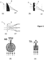
- There are also some components, which are able to perform both focusing and deviating functions simultaneously, such as asymmetric refractive lenses (see
Figure 1 (a) ), asymmetric diffractive lenses (seeFigure 1 (b) ), and diffractive gratings ((seeFigure 1 (c) ). - Devices embedding asymmetric refractive lenses (see
Figure 1 (a) ) rely on the phase delay experienced by the rays propagating through adielectric material 2 with a refractive index n2 higher than that (n1) of thehost medium 1. The transmitted rays focus in the focal plane FP. The optical power of such a component depends on the refractive index ratio at the boundaries of the lens, as well as on the curvature of its convex surface. Its effectiveness depends on the size, surface quality, and fabrication tolerance of the lens surfaces. The required fabrication accuracy can be achieved quite easily for large-size lenses, which dimensions are much larger than the wavelength (which is typical for optical applications). On the opposite, manufacturing asymmetric microlenses having wavelength-scale dimensions (which is typical for nano-photonic applications) is difficult, because the curvilinear shape of the lens profile is not always compatible with established micro- and nano-fabrication techniques. The use of refractive lenses in integrated focusing systems may also face certain difficulties because its operational principle requires ahost medium 1 with a refractive index n1 lower that that of thelens material 2, e.g. air. This may cause certain difficulties with fixation of the lenses in space and their alignment with respect to other focusing elements. - Devices embedding asymmetric diffractive lenses (see
Figure 1 (b) ) rely on the diffraction phenomenon. In particular, such lenses may take the form of a zoned dielectric plate with variable groove width, which can be optimized to provide a desired optical power and light deviation angle. The light deviating function is implemented by breaking the symmetry of the structure, similarly as in the case of asymmetric refractive lenses. Diffractive lenses have a planar technology that fits well both optical and nano-photonic applications. It is also compatible with established micro- and nano-scale fabrication techniques, such as photolithography. However, diffractive lenses intrinsically suffer from strong chromatic aberration that may not be acceptable for some applications. - Finally, a tilted focused beam can be generated by a diffraction grating 3 (see
Figure 1 (c) ). Such a grating can be implemented in the form of periodic grooves or strips, which period defines the light deviation angles observed for the first and higher diffraction orders. Such gratings are easy to implement, which makes them attractive for both optical and photonic applications. However, like diffractive lenses, they intrinsically suffer from chromatic aberrations. Moreover, the gratings always give rise to multiple beams associated with different diffraction orders, which may not be acceptable for some applications. - Moreover, as already mentioned above, an additional weakness of the devices of
figure 1 is that the spatial resolution of such far-field focusing systems is limited by the Abbe diffraction limit set by ∼λ/2n sina, where λ is the vacuum wavelength, n is the host media refractive index, and α is the half aperture angle of the lens. Thus, a higher resolution can be achieved either by increasing the lens aperture size or by reducing the focusing distance. The latter explains the growing interest to near-field focusing systems. This interest is also strongly supported by the growing number of applications across different domains, which require near-field light processing with the highest possible resolution, and notably subwavelength resolution (see for example the previous mentioned article "Photonic nanoiets"). - At present, there are several near-field focusing techniques available, based on subwavelength aperture probes (see the article " Near-field optical microscopy and spectroscopy with pointed probes", by L. Novotny and S.J. Stranick, published in the Annu. Rev. Phys. Chem. Vol. 57, pp. 303-331, 2006 or the article " Fabrication of optical fiber probes for scanning near-field optical microscopy", by S.Y. Guo, J.M. LeDue, P. Grütter, and published in mSURJ, vol. 3, no. 1, 2008.), planar subwavelength-patterned structures (see the document
US 8,003,965 or the article " Near-field plates: subdiffraction focusing with patterned surfaces" by A. Grbic, L. Jiang and R. Merlin, published in Science, vol. 320, pp. 511-513, 2008), and photonic nanojet microsphere dielectric lenses (see the article " Photonic nanoiet-enabled optical data storage" by S.-C. Kong et al., published in Opt. Express, Vol. 16, No. 18, 2008, or the documentUS 7,394,535 , (illustrated inFigure 1(d) ) or the previously mentioned article "Photonic nanojets"). The latter solution (i.e. nanojet microspheres (Figure 1(d) )) is often referred to as the most effective one because microspheres can simultaneously provide the subwavelength resolution and a high level of field intensity enhancement (also noted FIE). As shown onFigure 1(d) , they allow generating a nanojet beam NB. - Despite attractive performance characteristics, the use of microspheres is associated with certain difficulties related to their (i) precise positioning, (ii) integration with other optical components, and (iii) non-compatibility with the established planar fabrication techniques. These difficulties affect feasibility and increase the fabrication and assembly costs of the nanojet based devices. Potentially, the assembly problem can be solved using nanoscale patterned structures or hollow tubing (see the document
US 8,554,031 ), but these solutions may not be compatible with some applications. - An alternative solution for nanojet microsphere lenses was proposed based on the solid dielectric cuboids (noted SDC). As demonstrated in the article " Teraiets produced by dielectric cuboids" by V. Pacheco-Pena et al., published in Applied Phys. Lett. vol. 105, 084102, 2014 (and illustrated by
Figure 1(e) ), or in the article " Multifrequency focusing and wide angular scanning of teraiets" by V. Pacheco-Pena et al., published in Opt. Lett., vol. 40, no. 2, pp. 245-248, 2015, when illuminated by a plane wave, the SDC lenses can also produce condensed beams TB, similar to the nanojet beams observed for microspheres, with subwavelength dimensions, provided the size and shape of cuboids is properly adjusted with respect to the incident wavelength and the refractive index of the cuboid material. According to the previously mentioned article "Teraiets produced by dielectric cuboids", the best spatial resolution (λ/2, where λ is the wavelength in the host medium) and field intensity enhancement (factor of ∼10) is achieved for SDC with dimensions of about one wavelength in the host medium and the refractive index ratio n2/n1 ~ 1.5, where n1 and n2 are refractive indexes of the host medium and cuboid material, respectively. - Although the rectangular shape of SDC lenses can be advantageous for some planar fabrication methods (e.g. micromachining or lithography), the fabrication of SDC lenses operating in the optical range can be difficult or even impossible because of the following constraints:
- Strict requirements imposed on the cuboid size and shape;
- Absence of materials with the desired refractive indexes (in the optical range, the refractive index of common optical glass and plastics, which can be used as a host medium, varies from n1 ≈ 1.3 up to 2.0, whereas, according to the article "Terajets produced by dielectric cuboids", the desired value of the cuboid lens refractive index should be n2 ∼ 2.25 (follows from the suggested ratio n1 /n2=1.5 and the refractive index value of a standard glass n1 ≈ 1.5) that is out of range for standard optical materials;
- No solution provided for setting the position of such lenses in space. This is a critical point because of the miniature size of the cuboids.
- Moreover, for the time being, such near-field focusing components enabling the subwavelength resolution, do not allow producing the required light deviation function. As shown on
figures 1(d) and 1(e) , where the arrows schematically show formation of nanojet beams when such components are illuminated by a plane wave from below, and where the elongated "jetlike" shape corresponds to the focal region, such components produce nanojet beams, which axis nearly coincides with the incident wave propagation direction. - In "Geometric effect on photonic nanojet generated by dielectric microcylinders with non-cylindrical cross-sections", Optics Communications, vol. 380, 17 June 2016, pages 287-296, XP029694296, Liu Cheng-Yang et al. describe a geometric effect on photonic nanojet generated by dielectric microcylinders with non-cylindrical cross-sections.
- Patent document
US 2010/067842 discloses a solution to control a Bessel beam based on ferromagnetic control of a beam shaper. - Based on the above, it can be concluded that there is no reliable solution for providing simultaneously focusing and light deviation functions, while achieving sub-wavelength resolution and providing a simple topology compatible with established micro- and nano-fabrication techniques.
- It would hence be desirable to provide a technique enabling control over the field intensity distribution in the near zone, and notably for focusing electromagnetic waves and beam forming in the near zone, which would not suffer from these drawbacks, and which would allow controlling the deviation of the focused beam.
- References in the specification to "one embodiment", "an embodiment", "an example embodiment", indicate that the embodiment described may include a particular feature, structure, or characteristic, but every embodiment may not necessarily include the particular feature, structure, or characteristic. Moreover, such phrases are not necessarily referring to the same embodiment. Further, when a particular feature, structure, or characteristic is described in connection with an embodiment, it is submitted that it is within the knowledge of one skilled in the art to affect such feature, structure, or characteristic in connection with other embodiments whether or not explicitly described.
- The present disclosure is directed to a device for forming at least one tilted focused beam in a near zone, from an electromagnetic wave incident on said device.
- Such a device is remarkable in that it comprises at least one layer of dielectric material comprising at least partially at least one cavity, said at least one cavity being filled in with a medium having a refractive index lower than that of said dielectric material. Moreover, said at least one cavity comprises at least one base surface, defined with respect to an arrival direction of said electromagnetic wave, and at least one lateral surface. Said at least one base surface is delineated by a base edge line which comprises at least two opposite base edge line segments comprising at least one concave base edge line segment and at least one convex base edge line segment, which shape and/or orientation and/or associated base angles between said at least one base surface and said at least one lateral surface control an angular position of a projection of said at least one focused beam in a plane orthogonal to said arrival direction of said electromagnetic wave and comprising at least part of said at least one base surface, called an azimuth angle.
- The tilted focused beam is formed thanks to a recombination of nanojet beams originating from different portions of the concave base edge line, and a direction of the tilted focused beam is different from a direction of the incident electromagnetic wave.
- Hence, the present disclosure provides a new type of device for forming desired field intensity distribution in the near zone, with the aid of purely dielectric microstructures. More precisely, such devices are remarkable in that they provide simultaneously focusing and light deviation functions. In other words, they allow focusing electromagnetic waves and generating condensed low-dispersive optical beams (so-called nanojets) in the near zone from a plane electromagnetic wave incident on the device; they also allow controlling the azimuth angle of such nanojets, thanks to an appropriate choice of the parameters of the device's structure, namely the length and curvature of the concave and convex segments of the base edge line, as well as the base angles between the base and lateral surfaces of the cavity. Actually, the lateral surface of the cavity need not necessarily be vertical, and may show an angle with respect to the normal to the surface of the dielectric layer.
- By base edge line, it is meant here, and throughout the present document, both an actual base edge line, in case the bottom surface forms an angle with the lateral surface of the cavity, and a shadow, or imaginary, base edge line, in case there is a burr or a passing between the bottom surface and the lateral surface of the cavity, with a smooth rounded transition between both.
- The plane in which the azimuth angle is defined is a horizontal plane comprising the base surface of the cavity, in case the electromagnetic wave is incident normal to the base surface, and the base surface forms an angle with the lateral surface of the cavity. More generally, such a plane is orthogonal to the arrival direction of the incident EM wave, and substantially tangent to the base surface, in case the transition between the base surface and the lateral surface of the cavity is not sharp but somehow rounded.
- There is no restriction on the bottom surface of the dielectric layer, which may be plane, or not. The dielectric layer may notably be flexible.
- The medium filling the cavity may simply be air, another gas, vacuum, a liquid or any other material with a refractive index lower than that of the dielectric material.
- According to an embodiment of the present disclosure, a ratio between said refractive index of said medium filling said at least one cavity and said refractive index of said dielectric material contributes to controlling an angular position of a projection of said at least one focused beam in a vertical plane, called an elevation angle.
- Such an elevation angle not only depends on the ratio of refractive indexes, but also on the base angle of the cavity. It may also be influenced by the size/shape of the concave segment of the cavity's base surface edge line.
- Hence, such a device allows controlling both the azimuth and elevation angles of the focused beam, thus achieving a complete control of the electromagnetic wave deviation, which makes it very attractive for many nano-photonic applications.
- According to another embodiment, said at least one cavity is targeted to be cylindrical or cone-shaped (i.e. said at least one cavity is approximately cylindrical or cone-shaped) and said base edge line has a shape of a crescent moon, comprising a concave base edge line segment and a convex base edge line segment.
- By cylindrical cavity, it is meant here, and throughout this document, a cavity which shape is a generalized cylinder, i.e. a surface created by projecting a closed two-dimensional curve along an axis intersecting the plane of the curve. In other words, such a cylinder is not limited to a right circular cylinder but covers any type of cylinder, notably, but not exclusively, a cuboid or a prism for example. The cavity may also have the form of a cone. Its main axis may be orthogonal to the surface of the bottom of the cavity, or be tilted. Due to the fabrication tolerance, the cavities may also have imperfect shapes, and it must be understood, for example, that cavities targeted to be shaped as cylinders, may become cone-shaped cavities during the manufacturing process.
- Hence, the cavity may have the shape of a hollow cylinder with a crescent moon cross section. The base edge line of such a cavity comprises two line segments adjacent to the convex and concave surfaces of the cylindrical cavity. In this configuration, the convex segment of the base edge line produces a wide diverging beam of a conical type, while the concave segment of the base edge line acts like a focusing element producing a focused nanojet beam that is formed thanks to the recombination of the nanojet beams originating from different portions of the concave segment of the base edge line.
- Such a cavity with a crescent moon cross section is easy to manufacture through established microfabrication techniques (like molding (e.g. nanoimprinting) or photolithography) by superimposing (i.e. subtracting) two circular cylinders.
- According to a further embodiment, said at least one cavity belongs to at least one set of at least two cavities.
- Cavities may be arranged into arrays of cavities, or non-regular arrangements forming a peculiar pattern, in order to generate specific focused beams in the near zone, or an array of beams, which deviation may be controlled. Moreover, the arrays of cavities may be planar (with all base faces of all cavities lying in the same plane) or not, and can be made of identical cavities or not. Notably, the microstructure may comprise any number of cavities arranged in one plane (i.e. at a surface of a single plate) and placed far enough from each other to avoid electromagnetic coupling (i.e. at least a few wavelengths in the host medium). Thanks to this, each microcavity produces an independent nanojet beam, which parameters (Full Width at Half Maximum (FWHM) and deviation angle) depend on the parameters of the corresponding microcavity.
- According to yet a further embodiment, said cavities in said set are at least partly merged to form at least one arrangement of cavities.
- For example, cavities may be combined to form a periodic S-type curved groove, or a gear-type cavity formed by merging several cavities with a crescent moon shape. Such a gear may have different radii of concave segments or may only have two or three identical or non-identical concave segments.
- According to an embodiment, a device according to the present disclosure may also comprise several gear-type cavities, whether identical or not, rotated in horizontal plane. It may also comprise an arrangement of S-type grooves, whether of identical or non-identical shape, i.e. with a varying radius of concave segments. For example, such a device may comprise a first S-type curved groove with all identical segments of radius R1, a second S-type curved groove of all identical segments of radius R2, a third S-type curved groove of all identical segments of radius R3, etc. In an alternate embodiment, it may also comprise one or several S-type curved grooves, with radius of the concave segments varying along the groove.
- Hence, the shape of the cavity can be generalized towards a more complex structure comprising a set of crescent moon elements combined together. Such a structure can be designed to produce a more complex optical function, as well as for gaining additional degrees of freedom for near-field patterning and/or for simplifying the fabrication/assembly process.
- According to an embodiment, such a device further comprises at least one layer forming a substrate abutting said at least one layer of dielectric material.
- Such a substrate may contribute to the mechanical rigidity of the device.
- According to a further embodiment, such a device further comprises at least one layer forming a superstrate, said at least one layer of dielectric material being located between said substrate and said superstrate.
- Hence, the device may take the form of a planar optically-transparent element, comprising two glass or plastic plates (namely the substrate and the superstrate), between which a dielectric material with void or filled hollow microcavities is embedded. The superstrate may of course be non-planar, and follow the shape of the substrate for example. Actually, the pattern of the field intensity distribution generated by the device when illuminated by a plane wave incident normal to the base solely depends on the cavity base angle (or step angle), on the cavity cross-section shape, and on the index ratio between the dielectric material and the medium filling the cavity (or covering the lower part of the surface with respect to the step).
- It must be noted that the radiation of the beams will change for incline incidence of the plane wave, with a shape of the beam well preserved for the incident angles of about +/- 30°, depending on the size, base angle and curvature of the cavity base edge line.
- According to a further embodiment, said substrate and said superstrate are made of the same dielectric material as said at least one layer of dielectric material.
- According to yet a further embodiment, said dielectric material forming said at least one layer of dielectric material belongs to the group comprising:
- glass;
- plastic;
- a polymer material, such as PMMA (Poly(methyl methacrylate)) or PDMS (Polydimethylsiloxane);
- an organic or inorganic optically transparent electrically conducting material (such as indium tin oxide (ITO) or doped zinc oxide (ZnO) for example);
- ceramics.
- In these dielectric materials, no plasmonic effect can occur. It must be noted that air is not considered as a candidate dielectric material for the device according to the present disclosure.
- Such a device can hence be fabricated using standard dielectric materials, which are easy to find and inexpensive.
- According to an embodiment, a material of said superstrate belongs to the group comprising:
- glass;
- plastic;
- a polymer material;
- an organic or inorganic optically transparent electrically conducting material (such as indium tin oxide (ITO) or doped zinc oxide (ZnO) for example);
- a semiconductor material;
- a liquid;
- a gas;
- a gel.
- According to an embodiment, a material of said substrate belongs to the group comprising:
- glass;
- plastic;
- a polymer material;
- an organic or inorganic optically transparent electrically conducting material (such as indium tin oxide (ITO) or doped zinc oxide (ZnO) for example);
- a semiconductor material;
- a liquid;
- a gas;
- a gel.
- Hence, no plasmonic effect can occur in said superstrate.
- According to an embodiment, the medium having a refractive index lower than that of said dielectric material belongs to the group comprising:
- glass;
- plastic;
- a liquid;
- a gas;
- a gel.
- It is to be understood that both the foregoing general description and the following detailed description are exemplary and explanatory and are not restrictive of the invention, as claimed.
- Embodiments of the present disclosure can be better understood with reference to the following description and drawings, given by way of example and not limiting the scope of protection, and in which:
-
Figures 1 (a), (b), (c), (d) and (e) relate to prior art techniques and are schematic drawings illustrating operational principles of refractive lenses, diffractive lenses, diffractive gratings, nanojet microlenses and terajet solid cuboid lenses; -
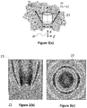
Figure 2(a) illustrates the topology of a hollow cylindrical cavity formed in a layer of dielectric material and producing a conical-type nanojet beam when illuminated by a plane wave from below, whilefigure 2(b) illustrates the normalized near-field power density distribution in the vertical xz-plane andfigure 2(c) illustrates the normalized power density distribution in the horizontal xy-plane; -
Figures 3A and 3B respectively show a 3D view and a top view of a device for forming a tilted focused beam in the near-zone according to an embodiment of the present disclosure; -
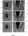
Figures 4(a), (b) and (c) present normalized near-field power density distribution in horizontal and vertical planes for the nanojet microlens offigures 3A and 3B illuminated by a linearly polarized plane wave from below, at different wavelengths; -
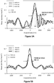
Figures 5A and 5B present the nanojet beam profile, as generated by the device offigures 3A and 3B , along the x-axis (figure 5A ) and along the γ-axis (figure 5B ); -
Figure 6 presents the peak power density in the nanojet beams produced by the convex and concave segments of the nanojet device with a crescent moon shape offigure 3 ; -
Figure 7 provides an alternate embodiment tofigure 3 , in which the device presents a variable base angle; -
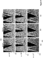
Figures 8(a) to 8(c) show the normalized field intensity patterns in xz-plane of the nanojet beam created by the device offigure 7 , for different values of the base angle and different wavelengths of an incident TE-polarized plane wave; -
Figures 9(a) to 9(c) show the normalized field intensity patterns in xz-plane of the nanojet beam created by the device offigure 7 , for different values of the base angle and different wavelengths of an incident TM-polarized plane wave; -
Figures 10(a) and10(b) illustrate the normalized field intensity profiles in an imaging plane at z=750nm for the device offigure 7 for different base angles when illuminated by a plane wave, which propagation direction coincides with the positive z-direction, respectively for a TE-polarized plane wave (figure 10(a) ) and for a TM-polarized plane wave (figure 10(b) ); -
Figures 11(a) and 11(b) illustrate the nanojet beam radiation angle with respect to the step base angle of the device offigure 7 for three different wavelengths, respectively for a TE polarization (Figure 11(a) ), and for a TM polarization (figure 11(b) ); -
Figures 12(a) to 12(d) illustrate an alternate embodiment to the device offigures 3A and 3B , according to which several devices with a crescent-moon shape are assembled in order to form a periodic S-type curved groove in a host dielectric medium; -
Figures 13(a) to 13(c) illustrate a further alternate embodiment to the device offigures 3A and 3B , according to which several devices with a crescent moon shape are assembled in order to form a cavity with a gear-type cross section. - The components in the figures are not necessarily to scale, emphasis instead being placed upon illustrating the principles of the invention.
- The general principle of the present disclosure relies on the design of a new dielectric microstructure, which may be used for generating condensed low-dispersive optical beams in the near zone, also called nanojets, while simultaneously controlling their deviation. Its use is not limited to optical wavelengths. Presence of hollow cavities in the dielectric microstructure gives rise to a diffraction phenomenon, which is in turn coupled to refraction and interference phenomena, and allows generating condensed beam(s) of radiation in the near zone, with a controlled deviation, when the dielectric microstructure is illuminated by a plane wave, depending on the shape and dimensions of the structure.
- The beam-forming and deviation function of such nanojet devices may be controlled by setting the cavity's base edge line length and curvature, as well as its base angle.
- Such a general principle allows designing new focusing and beam-forming components, which can replace the conventional focusing devices in dense optic and photonic systems, like integrated optical sensors used in photo/video cameras that are essential components in the field of mobile technology (e.g. smartphones, tablets, AR and VR glasses).
- Thanks to the ultra-compact dimensions of such dielectric microstructures, as well as to the wide range and diversity of field patterns, which can be produced through the use of such microstructures, the present disclosure finds applications in many fields of technology, including, but not limited to:
- eyewear electronics, including AR and VR glasses;
- optical sensors for photo/video/light field cameras;
- light communication systems, including quantum computers;
- bio/chemical sensors, including lab-on-chip sensors;
- microscopy, spectroscopy and metrology systems;
- integrated lens antennas for applications in the millimeter/submillimeter/infrared (IR) wavelength ranges.
- The following discussion mostly focuses on optical applications and thus refers to material properties and fabrication methods relevant to nanoscale structures and wavelength. Nevertheless, the proposed design concepts can be easily scaled to other wavelength ranges, including microwaves, mm-waves, THz, IR, visible light and UV.
- Inventors of the present disclosure have reached the conclusion that diffraction of a plane electromagnetic wave on the base surface of a dielectric material in the close vicinity of an abrupt change of level of this surface, also called a step, can result in the formation of condensed optical beams (so-called nanojets), when the surface on which diffraction occurs is in contact with a medium (material or gas) having a lower refractive index than that of the dielectric material. The number of beams and shape of each individual beam can be controlled by the variation of the step size and shape of the step edge line adjacent to the lateral and lower surfaces of the step. Unlike the well-known diffracted beams predicted by the Fresnel theory, the nanojet beams are low-dispersive (they show no or small wavelength dependence). Moreover, a same nanojet focusing component according to the present disclosure can produce multiple independent beams (having identical or non-identical shape) associated with different segments of the step edge line, which is not possible with Fresnel diffractive lenses. These unique features make the nanojet-based focusing components according to the present disclosure attractive for many today and future applications.
-
Figures 2(a) to 2(c) illustrate this general principle, according to which diffraction of a plane wave by a hollow cylindrical cavity as shown onfigure 2(a) , created in a dielectric host medium, results in the formation of a focused beam (i.e. nanojet), whose cross-section shape in the plane orthogonal to the incident wave propagation direction reproduces the shape of the cavity base edge line. - In
figure 2(a) , a hollowcylindrical cavity 22 with height H=740 nm and radius R=370 nm is created in adielectric host medium 21 with refractive index n1=1.5. The refractive index inside thehollow cavity 22 is n2<n1, n2=1. Thecavity 22 has a circular cross-section. - When a
plane wave 20 is incident from below, thecavity 22 produces a hollowconical nanojet beam 23, whose opening angle (i.e. light deviation angle) depends on the index ratio between themedia 22 inside and themedia 21 outside the cavity. This phenomenon, as well as the shape of the nanojet beam thus produced is illustrated byfigures 2(b) and 2(c) , which respectively show the normalized near-field power density distribution in the vertical xz-plane and the normalized power density distribution in the horizontal xy-plane at z=zo=100 nm. - However, with such a hollow cylindrical cavity of circular cross-section, it is not possible to control the azimuth and elevation angle of the
nanojet beam 23. Nonetheless, diffraction of light on a cavity, created in a dielectric host medium having refractive index n1 and filled in with a dielectric material having refractive index n2<n1 can result in formation of a tilted nanojet beam, whose deviation angle (defined with respect to the incident wave propagation direction) can be predicted by the following equation:

- Actually, the
nanojet beam 23 is created as a result of the interference between a refracted wave, which is radiated outside thecavity 22 and the plane wave incident from below. As a consequence, the angle of radiation of the nanojet beam (θB ) is defined by a vector sum of these two waves. Moreover, the refraction angle of the wave radiated outward the cavity is close to the critical angle for the wave incident on the same boundary from outside: θ1 ≈ θTIR, since the main contribution to the formation of the planar wave front of the refracted wave outside the cavity comes from Huygens sources located close to the lateral edge of thecavity 22. - Moreover, the peak field intensity in the nanojet beam depends on the dimensions of the cavity, base angle, and curvature of its base edge line.
- According to the present disclosure, and as illustrated by
figures 3A and 3B , a new type of nanojet microlens is hence introduced, whose shape resembles young moon, and which provides control over the azimuth and elevation angles of the focused nanojet beam. -
Figure 3A provides a 3D view of such a nanojet microlens with schematic illustration of the individual nanojet beams associated with different portions of the base edge line. Acylindrical cavity 32 is formed in adielectric host medium 31 with refractive index n1>n2, where n2 is the refractive index of the medium filling thecavity 32, for example air with n2=1. More generally, the cavity can be filled in with any dielectric material (air, gas, glass, plastic, polymers, liquid...) having a refractive index lower than that of thedielectric host medium 31. Thebase surface 321 of thecavity 32 is delineated by abase edge line 322, represented by a piecewise curve which comprises at least one convex part and at least one concave part. Infigure 3A , thebase edge line 322 comprises two line segments adjacent to the convex and concave surfaces of thecylindrical cavity 32. In this configuration, the convex segment of the base edge line 322 (formed by baseedge line segments figures 2(a) to 2(c) , and comprising the nanojet beams 331, 332, 333. Theconcave segment 3224 of thebase edge line 322 acts like a focusing element producing a focusedNJ beam 334, which is formed thanks to the recombination of the NJ beams originating from different portions of theconcave segment 3224 of thebase edge line 322. - The radiation angle of the
nanojet beam 334, i.e. light deviation angle in the vertical (elevation) plane, is mainly defined by the index ratio at the boundary of thecavity 32. It also depends on the base angle of the cavity and, possibly, on the size/shape of the concave segment of its base surface edge line. - Orientation of the beam in the horizontal (azimuthal) plane can be varied by rotating the moon-like cavity around its vertical axis (i.e. z-axis in
figures 3A- 3B). In this case, orientation of the nanojet beam in the horizontal plane can be characterized by an azimuth angle counted with respect to x-axis. - As illustrated in
figure 3B , the lens with a crescent moon shape is created by superimposing (i.e. subtracting) two circular cylinders 341, 342 having the same height but different radii R1 and R2. The distance between both cylinders 341, 342 is a variable parameter W. In the following discussion, for sake of simplicity, it is assumed that R1=R2=W. - The following figures illustrate the results of full-wave 3D-FDTD (for "Finite Difference Time Domain") performed using the model of
figures 3A and 3B , computed using CST software (Computer Simulation technology v. 15). - More precisely,
figures 4(a) to 4(c) present normalized near-field power density distribution in horizontal and vertical planes for the microlens offigures 3A and 3B illuminated by a linearly polarized plane wave from below, at different wavelengths, namelyλ 0 = 450nm forfigure 4(a) , λ 0 = 550nm forfigure 4(b) and λ 0 = 650nm forfigure 4(c) . - More precisely, the left images correspond to the simulated normalized power density distribution in xy-plane at z=zo, and the right images in xz-plane at y=0.
- The parameters of the structure are n1=1.5, n2=1, H=500nm, R1=R2=W=800nm. The imaging plane position is z0=900nm.
- As may be observed in
figure 4 , the power density distribution in the near zone of a hollow cavity with a crescent moon shape agrees well with the theoretical model presented infigures 3A and 3B . In particular, a tiltedfocused beam 334 can be identified on the concave side of thecavity 32. The shape of the beam is well preserved from λ 0 = 450nm to λ 0 = 650nm. -
Figures 5A and 5B present simulated near-field power density distribution in xy-plane (at z=z0) along two lines parallel to x- and y-axes crossing at the point with a maximum power density as observed at λ 0 = 550nm. Dimensions of the structure are the same as infigure 4 , namely n1=1.5, n2=1, H=500nm, R1=R2=W=800nm. The imaging plane position is z0=900nm. More precisely,figure 5A illustrates the power density, expressed in mW/m2, as a function of the x-coordinate, expressed in nm, for y=0nm and zm=900nm, at three different wavelengths, namely 450nm, 550nm and 650nm.Figure 5B illustrates the power density, expressed in mW/m2, as a function of the y-coordinate, expressed in nm, for xm=580nm and zm=900nm, at three different wavelengths, namely 450nm, 550nm and 650nm. The beam full width at half maximum (FWHM) is about 480nm in both planes. -
Figure 6 presents the peak power density (expressed in mW/m2) in the nanojet beams produced by the convex (curve 62) and concave (curve 61) segments of the crescent moon-like nanojet device offigures 3A and 3B , defined as a maximum power density in xz-plane for y<0 and y>0 respectively, as a function of the radius R1=R2=W expressed in nanometers. As may be observed, a radius of 800nm gives good performance. Two reference solutions are also shown, which correspond to the power density of a plane wave propagating in the same host medium (line 63) and to a nanojet beam produced by a straight edge of an infinite groove (line 64). -
Figures 7 to 11 illustrate the existing relation between the cavity base angle of the nanojet device and the nanojet beam radiation angle. -
Figure 7 first gives some notations, which will be used thereafter. Acavity 32 is formed in adielectric host medium 31.Cavity 32 comprises a base surface, or lower part, 321 and alateral part 323, which forms abase angle 70 α with thebase surface 321. Thecavity 32 forms a step, i.e. an abrupt change of level in thedielectric host medium 31. It is considered infigure 7 that the step is infinite along y-direction, as compared to the wavelength of the incidentelectromagnetic wave 20. The cavity edge lines extend to infinity in the negative x- and positive z-directions, as compared to the wavelength. - A
nanojet beam 334 is produced by this step withbase angle 70 α. It shows aradiation angle 71, noted as θB, measured from the z axis. -
Figures 8(a) to 8(c) show the normalized field intensity patterns in xz-plane of the nanojet beam created by the device offigure 7 , for different values of thebase angle 70 α and different wavelengths of theincident EM wave 20. It is considered that theincident EM wave 20 is a TE-polarized plane wave, and that the refractive index of the host medium is n1=1.5.Figure 8(a) shows the normalized field intensity pattern in xz-plane for a wavelength of theEM wave 20 λ 0 = 450nm;figure 8(b) shows the normalized field intensity pattern in xz-plane for a wavelength of theEM wave 20 λ 0 = 550nm;figure 8(c) shows the normalized field intensity pattern in xz-plane for a wavelength of theEM wave 20 λ 0 = 650nm. The top row of images corresponds to abase angle 70 α = 70°, the middle row of images corresponds to abase angle 70 α = 90°, and the bottom row of images corresponds to abase angle 70 α = 110°. -
Figures 9(a) to 9(c) show the normalized field intensity patterns in xz-plane of the nanojet beam created by the device offigure 7 , for different values of thebase angle 70 α and different wavelength of theincident EM wave 20. It is now considered that theincident EM wave 20 is a TM-polarized plane wave, and that the refractive index of the host medium is n1=1.5.Figure 9(a) shows the normalized field intensity pattern in xz-plane for a wavelength of theEM wave 20 λ 0 = 450nm;figure 9(b) shows the normalized field intensity pattern in xz-plane for a wavelength of the EM wave 20λ 0 = 550nm;figure 9(c) shows the normalized field intensity pattern in xz-plane for a wavelength of theEM wave 20 λ 0 = 650nm. The top row of images corresponds to abase angle 70 α = 70°, the middle row of images corresponds to abase angle 70 α = 90°, and the bottom row of images corresponds to abase angle 70 α = 110°. - As may be observed on
figures 8(a) to 8(c) and9(a) to 9(c) , the value of thebase angle 70 α thus influences the radiation angle of the nanojet beam created by the step of the device offigure 7 . -
Figures 10(a) and10(b) illustrate the normalized field intensity profiles in an imaging plane at z=750nm for the device offigure 7 for different values of thebase angle 70 α when illuminated by a plane wave, which propagation direction coincides with the positive z-direction, respectively for a TE-polarized plane wave (figure 10(a) ) and for a TM-polarized plane wave (figure 10(b) ). The refractive index of the host medium is n1=1.5, and the wavelength of the incident wave is λ 0 = 450nm. The x axis corresponds to the x coordinates expressed in nm. -
Figures 11(a) and 11(b) illustrate the nanojet beam radiation angle θ expressed in degrees with respect to thestep base angle 70 α, also expressed in degrees, for three different wavelengths, namely 450nm, 550nm and 650nm.Figure 11(a) corresponds to a TE polarization, andfigure 11(b) corresponds to a TM polarization of theincident EM wave 20. The refractive index of the host medium is n1=1.5. - In
figures 11(a) and (b) , the nanojet beam radiation angle is defined as follows:

figure 7 . - Based on the data reported in
figures 11(a) and (b) , the nanojet radiation angle can be estimated as:
- For the selected configuration of the
cavity 32, the mismatch between Eq. (4) and the data extracted from the full-wave EM simulations does not exceed 3° for all values of thebase angle 70 α. - The nanojet microlenses with crescent moon shape according to the present disclosure are near-zone focusing devices, which are used in association with other optical elements, such as focusing, beam-forming, light guiding or light capturing components. To increase their overall efficiency, it may be advantageous to use arrays of such nanojet elements, which may comprise from a few to several hundreds of cavities. These arrangements of moon-like nanojet microlenses can be created either on surface of the component tor inside the volume.
- Hence, a device according to an embodiment of the present disclosure may comprise any number of cavities arranged in one plane (i.e. at a surface of a single plate) and placed far enough from each other to avoid electromagnetic coupling (i.e. at least a few wavelength in the host medium). Thanks to this, each microcavity will produce an independent nanojet beam, which parameters (FWHM and deviation angle) will depend on the parameters of the corresponding microcavity.
- Multi-layers structures with two or more arrangements of nanojet microcavities arranged in different horizontal planes are also possible.
- In some embodiments, it may be preferable to arrange the nanojet cavities so as to form an array, either with a regular or an irregular layout. Such an array may comprise any number of identical or non-identical cavities (in terms of size, shape and orientation). For instance, it can comprise identical nanojet cavities with a crescent moon shape with different orientation or an array of groups of nanojet cavities arranged in accordance to a determined pattern in order to produce a more complex optical function. This can be a certain near-field pattern or a larger-scale focused beam, produced as a result of recombination of independent nanojet beams associated with different microcavities, that extends beyond the near-zone of a single nanojet microlens.
- The shape of the nanojet cavity can also be generalized towards a more complex structure comprising a set of moon-like elements combined together. Such a structure can be designed to produce a complex optical function, as discussed above, or for gaining additional degrees of freedom for near-field patterning and/or for simplifying the fabrication/assembly process.
-
Figures 12 and 13 show possible examples of such arrangements of moon-like nanojet microlenses. -
Figures 12(a) to 12(d) illustrate an alternate embodiment to the device offigures 3A and 3B , according to which several devices with a crescent-moon shape are assembled in order to form a periodic S-type curved groove in a host dielectric medium. -
Figure 12(a) presents a perspective view of adielectric plate 121, within which a generalized crescent moon like focusing element having a form of a periodic S-typecurved groove 122 is created. More precisely,figure 12(a) shows the topology of a unit cell of such a periodic groove, placed infree space 123, and engraved at the surface of adielectric substrate 121. -
Figure 12(b) illustrates the near-field intensity pattern in xy-plane at a close distance above theplate surface 121. -
Figure 12(c) provides a 3D view of the field intensity pattern of the unit cell offigure 12(a) . -
Figure 12(d) illustrates the field intensity pattern in a 2D xz-plane crossing a nanojet beam. - In the embodiment of
figures 12(a) to 12(d) , the host medium refractive index is ni=1.5, the groove depth is H=500nm, the groove width is W=400nm and the wavelength of theEM incident wave 120 is λ 0 = 500nm. - As detailed in
Figures 12(a) and 12(b) , the periodic S-typecurved groove 122 is formed by a cavity that comprises at least one base surface, defined with respect to an arrival direction of said electromagnetic wave, and at least one lateral surface, and said at least one base surface is delineated by a base edge line which has portions, each portion having a U-shape or C-shape or a crescent moon-shape (depending of the viewing orientation), that comprises a concave base edge line segment and a convex base edge line segment. -
Figures 13(a) to 13(c) illustrate a further alternate embodiment, according to which several devices with a crescent moon shape are assembled in order to form a cavity with a gear-type cross section with four identical concave segments, created in a double-layer dielectric plate. - More precisely,
figure 13(a) illustrates the topology of such a gear-type cavity 132, created in adielectric plate 131.Figure 13(b) shows the near-field intensity pattern in xy-plane at a close distance above theplate 131 surface;figure 13(c) shows the field intensity pattern in xz-plane passing through the center of thecavity 132 and its concave segments. In the embodiment offigures 13(a) to 13(c) , the host medium refractive index n 1 = 1.5, and the dimensions of thecavity 132 are as follows: external radius R 1=1500nm, radius of curvature of the concave parts R 2=400nm, depth H=600nm, groove width W=400nm. The wavelength of theEM incident wave 130 is λ 0 = 532nm. - As detailed in
Figures 13(a) and 13(b) , the gear-type cavity 132 comprises at least one base surface, defined with respect to an arrival direction of said electromagnetic wave, and at least one lateral surface, and said at least one base surface is delineated by a base edge line which has at least four portions that have a U-shape or C-shape or a crescent moon-shape (depending of the viewing orientation), that comprises a concave base edge line segment and a convex base edge line segment. - According to embodiments of the present disclosure, such devices embedding one or several cavities with a crescent moon shape in a dielectric microstructure can be fabricated using any established microfabrication technique, like molding (e.g. nanoimprinting) or photolithography.
- According to an embodiment, such a component can take the form of a plate made of an optically transparent material (e.g. glass, plastic, polymer) with a microstructure formed on one of its surfaces. The plate can be planar or curved, flexible (bendable). The plate can be made of a single material or may comprise several layers. The former option is more suitable for resist-free molding fabrication methods, while the latter is more relevant to photolithography techniques.
- In some embodiments, the plate with engraved microstructure can be attached to another component, e.g. another dielectric plate or a plano-convex lens. In such a case, the nanojet cavities may be formed on the external surface of the compound component, or at the interface between the two attached components.
- Hence, the proposed component, in all its embodiments, can be, for instance, fabricated in the form of a thin film with perforated apertures attached to a glass plate or directly to a surface of another optical component, e.g. a plano-convex lens. It can also be covered with another layer of an optically-transparent media (e.g. another glass plate).
- The film can be made of an optically transparent material, like PMMA (Acrylic), that is to be deposited directly on the surface of the supporting component (e.g. glass plate or lens). For instance, this can be done by spin-coating that enables deposition of thin nanofilms with the desired thickness (order of a few hundred nanometers).
- The apertures (that will serve as hollow cuboids) can then be created, for instance, using the optical or e-beam lithography technology.
- The periodic structures can be, potentially, fabricated using the maskless interference lithography that is faster and cheaper than standard optical lithography.
- In an alternate embodiment, the cavities with a crescent moon shape can be fabricated using nanoimprinting or replica molding methods in an optically transparent material, e.g. soft organic polymer such as PDMS, and then attached to a surface of a glass plate acting as a support.
-
Figure 14 presents an example of a device that can be used to control the performance of a device according to one embodiment of the disclosure. - Such a device referenced 1400 comprises a computing unit (for example a CPU, for "Central Processing Unit"), referenced 1401, and one or more memory units (for example a RAM (for "Random Access Memory") block in which intermediate results can be stored temporarily during the execution of instructions a computer program, or a ROM block in which, among other things, computer programs are stored, or an EEPROM ("Electrically-Erasable Programmable Read-Only Memory") block, or a flash block) referenced 1402. Computer programs are made of instructions that can be executed by the computing unit. Such a
device 1400 can also comprise a dedicated unit, referenced 1403, constituting an input-output interface to allow thedevice 1400 to communicate with other devices. In particular, thisdedicated unit 1403 can be connected with an antenna (in order to perform communication without contacts), with light source/receiving unit (such as for example a photodiode, optical fiber, detector, e.g. photodiode, etc.) or with serial ports (to carry communications "contact"). It should be noted that the arrows inFigure 14 signify that the linked units can for example exchange data together through buses. - In an alternate embodiment, control of the performance of a device according to one embodiment of the disclosure can be implemented in hardware in a programmable FPGA ("Field Programmable Gate Array") component or ASIC ("Application-Specific Integrated Circuit") component.
Claims (11)
- A device for forming at least one tilted focused beam (334) in a near-field zone, from an electromagnetic wave (20) incident on said device,said device being characterized in that it comprises at least one layer of dielectric material (31) comprising at least partially at least one cavity (32), said at least one cavity being filled in with a medium having a first refractive index lower than a second refractive index of said dielectric material (31),wherein said at least one cavity is approximately cylindrical or cone-shaped and comprises at least one base surface (321), defined with respect to an arrival direction of said electromagnetic wave, and at least one lateral surface (323),wherein said at least one base surface is delineated by a base edge line (322) that has a shape of a crescent moon, said base edge line comprising a concave base edge line segment (3224) and a convex base edge line segment (3221-3223),wherein one or more of a shape of said base edge line, an orientation of said at least one cavity, and associated base angles between said at least one base surface and said at least one lateral surface control an azimuth angle of said at least one tilted focused beam (334), the azimuth angle defined by an angular position of a projection of said at least one tilted focused beam on a plane orthogonal to said arrival direction of said electromagnetic wave and comprising at least part of said at least one base surface,and wherein said at least one tilted focused beam is formed as a result of a recombination of nanojet beams originating from different portions of said concave base edge line segment, and wherein a direction of said at least one tilted focused beam is different from a direction of said incident electromagnetic wave.
- The device for forming at least one tilted focused beam in a near-field zone according to claim 1, wherein a ratio between said first refractive index of said medium filling said at least one cavity (32) and said second refractive index of said dielectric material (31) contributes to controlling an elevation angle of said at least one tilted focused beam, said elevation angle defined by said angular position of said projection of said at least one tilted focused beam in a vertical plane.
- The device for forming at least one tilted focused beam in a near-field zone according to any of claims 1 and 2, wherein said at least one cavity (32) belongs to a set of at least two cavities.
- The device for forming at least one tilted focused beam in a near-field zone according to claim 3, wherein said at least two cavities in said set are at least partly merged to form at least one arrangement of cavities.
- The device for forming at least one tilted focused beam in a near-field zone according to any of claims 1 to 4, wherein the device further comprises at least one layer forming a substrate (121) abutting said at least one layer of dielectric material (31).
- The device for forming at least one tilted focused beam in a near-field zone according to claim 5, wherein the device further comprises at least one layer forming a superstrate, said at least one layer of dielectric material (31) being located between said substrate and said superstrate.
- The device for forming at least one tilted focused beam in a near-field zone according to claim 6, wherein said substrate and said superstrate are made of the same dielectric material as that of said at least one layer of dielectric material.
- The device for forming at least one tilted focused beam in a near-field zone according to any of claims 1 to 7, wherein a material forming said at least one layer of dielectric material (31) is selected from the group consisting of: a glass, a plastic, a polymer material, an organic optically transparent electrically conducting material, an inorganic optically transparent electrically conducting material, and a ceramic material.
- The device for forming at least one tilted focused beam in a near-field zone according to any of claims 6 and 7, wherein a material of said superstrate is selected from the group consisting of: a glass, a plastic, a polymer material, an organic optically transparent electrically conducting material, an inorganic optically transparent electrically conducting material, a liquid, a gas, and a gel.
- The device for forming at least one tilted focused beam in a near-field zone according to any of claims 5 to 7, wherein a material of said substrate is selected from the group consisting of: a glass, a plastic, a polymer material, an organic optically transparent electrically conducting material, an inorganic optically transparent electrically conducting material, a semiconductor material, a gas, and a gel.
- The device for forming at least one tilted focused beam in a near-field zone according to any of claims 1 to 10, wherein said medium having said first refractive index lower than said second refractive index of said dielectric material (31) is selected from the group consisting of: a glass, a plastic, a liquid, a gas, and a gel.
Applications Claiming Priority (2)
| Application Number | Priority Date | Filing Date | Title |
|---|---|---|---|
| EP16306387.8A EP3312660A1 (en) | 2016-10-21 | 2016-10-21 | Device for forming at least one tilted focused beam in the near zone, from incident electromagnetic waves |
| PCT/EP2017/076877 WO2018073426A1 (en) | 2016-10-21 | 2017-10-20 | Device for forming at least one tilted focused beam in the near zone, from incident electromagnetic waves |
Publications (2)
| Publication Number | Publication Date |
|---|---|
| EP3529657A1 EP3529657A1 (en) | 2019-08-28 |
| EP3529657B1 true EP3529657B1 (en) | 2021-12-15 |
Family
ID=57944243
Family Applications (2)
| Application Number | Title | Priority Date | Filing Date |
|---|---|---|---|
| EP16306387.8A Withdrawn EP3312660A1 (en) | 2016-10-21 | 2016-10-21 | Device for forming at least one tilted focused beam in the near zone, from incident electromagnetic waves |
| EP17784325.7A Active EP3529657B1 (en) | 2016-10-21 | 2017-10-20 | Device for forming at least one tilted focused beam in the near zone, from incident electromagnetic waves |
Family Applications Before (1)
| Application Number | Title | Priority Date | Filing Date |
|---|---|---|---|
| EP16306387.8A Withdrawn EP3312660A1 (en) | 2016-10-21 | 2016-10-21 | Device for forming at least one tilted focused beam in the near zone, from incident electromagnetic waves |
Country Status (4)
| Country | Link |
|---|---|
| US (1) | US11275252B2 (en) |
| EP (2) | EP3312660A1 (en) |
| CN (1) | CN110168432B (en) |
| WO (1) | WO2018073426A1 (en) |
Cited By (1)
| Publication number | Priority date | Publication date | Assignee | Title |
|---|---|---|---|---|
| RU2809980C1 (en) * | 2023-05-24 | 2023-12-20 | Федеральное государственное бюджетное образовательное учреждение высшего образования "Сибирский государственный университет геосистем и технологий" | Method and device for forming inclined photon jet formed by meso-sized particle |
Families Citing this family (22)
| Publication number | Priority date | Publication date | Assignee | Title |
|---|---|---|---|---|
| EP3223063A1 (en) | 2016-03-24 | 2017-09-27 | Thomson Licensing | Device for forming a field intensity pattern in the near zone, from incident electromagnetic waves |
| EP3312660A1 (en) | 2016-10-21 | 2018-04-25 | Thomson Licensing | Device for forming at least one tilted focused beam in the near zone, from incident electromagnetic waves |
| EP3312646A1 (en) | 2016-10-21 | 2018-04-25 | Thomson Licensing | Device and method for shielding at least one sub-wavelength-scale object from an incident electromagnetic wave |
| US10242503B2 (en) | 2017-01-09 | 2019-03-26 | Snap Inc. | Surface aware lens |
| EP3385219B1 (en) | 2017-04-07 | 2021-07-14 | InterDigital CE Patent Holdings | Method for manufacturing a device for forming at least one focused beam in a near zone |
| EP3451027A1 (en) | 2017-09-01 | 2019-03-06 | Thomson Licensing | Optical device capable of providing at least two different optical functions |
| EP3540479A1 (en) | 2018-03-13 | 2019-09-18 | Thomson Licensing | Diffraction grating comprising double-materials structures |
| EP3540499A1 (en) | 2018-03-13 | 2019-09-18 | Thomson Licensing | Image sensor comprising a color splitter with two different refractive indexes |
| EP3591700A1 (en) | 2018-07-02 | 2020-01-08 | Thomson Licensing | Image sensor comprising a color splitter with two different refractive indexes, and different height |
| US11030813B2 (en) | 2018-08-30 | 2021-06-08 | Snap Inc. | Video clip object tracking |
| EP3632564A1 (en) | 2018-10-01 | 2020-04-08 | Thomson Licensing | System for optical detection and imaging of nanoscale objects |
| EP3633437A1 (en) * | 2018-10-01 | 2020-04-08 | InterDigital CE Patent Holdings | Device for near-field focusing and beam forming |
| EP3633438A1 (en) * | 2018-10-01 | 2020-04-08 | InterDigital CE Patent Holdings | Inhomogeneous microlens device for near-field focusing, beam forming, and high-efficiency far-field device implementation |
| US11176737B2 (en) | 2018-11-27 | 2021-11-16 | Snap Inc. | Textured mesh building |
| EP3671310A1 (en) * | 2018-12-18 | 2020-06-24 | Thomson Licensing | Optical manipulation apparatus for trapping or moving micro or nanoparticles |
| EP3671322A1 (en) * | 2018-12-18 | 2020-06-24 | Thomson Licensing | Device for forming an outgoing electromagnetic wave from an incident electromagnetic wave |
| EP3671321A1 (en) | 2018-12-18 | 2020-06-24 | Thomson Licensing | Device for forming at least one tilted focused beam in the near-field zone, from incident electromagnetic waves, and image sensor including such a device |
| CN113330484A (en) | 2018-12-20 | 2021-08-31 | 斯纳普公司 | Virtual surface modification |
| US11189098B2 (en) * | 2019-06-28 | 2021-11-30 | Snap Inc. | 3D object camera customization system |
| CN110829035B (en) * | 2019-11-19 | 2021-03-16 | 大连海事大学 | Circular polarization patch antenna of wide half-power wave beam |
| US11227442B1 (en) | 2019-12-19 | 2022-01-18 | Snap Inc. | 3D captions with semantic graphical elements |
| CN113181556B (en) * | 2021-04-30 | 2022-09-23 | 西北核技术研究所 | Irradiation cavity based on medium substrate structure and used for enhancing field intensity in large effector |
Family Cites Families (85)
| Publication number | Priority date | Publication date | Assignee | Title |
|---|---|---|---|---|
| US3873408A (en) | 1969-10-06 | 1975-03-25 | Bausch & Lomb | Method of producing a refractive index gradient in glass |
| US3718383A (en) | 1971-04-19 | 1973-02-27 | Eastman Kodak Co | Plastic optical element having refractive index gradient |
| US3904268A (en) | 1974-11-15 | 1975-09-09 | Corning Glass Works | Optical waveguide having optimal index gradient |
| DE3607259A1 (en) | 1985-03-05 | 1986-09-18 | Nippon Sheet Glass Co. Ltd., Osaka | MICRO LENS PLATE AND METHOD FOR THEIR PRODUCTION |
| US6753131B1 (en) | 1996-07-22 | 2004-06-22 | President And Fellows Of Harvard College | Transparent elastomeric, contact-mode photolithography mask, sensor, and wavefront engineering element |
| DE69724159T2 (en) | 1997-09-19 | 2004-05-06 | International Business Machines Corp. | OPTICAL LITHOGRAPHY WITH EXTREMELY HIGH RESOLUTION |
| US6236513B1 (en) | 1999-06-30 | 2001-05-22 | Quantum Corporation | Integrated objective/solid immersion lens for near field recording |
| EP1266247A4 (en) * | 2000-02-02 | 2009-09-30 | Brilliant Film Llc | Multiflecting light directing film |
| US6804189B2 (en) | 2000-04-07 | 2004-10-12 | Tosoh Corporation | Near field optical recording medium |
| US6594430B1 (en) | 2000-05-11 | 2003-07-15 | Carnegie Mellon University | Solid immersion lenses for focusing collimated light in the near-field region |
| EP1414339B1 (en) | 2001-07-26 | 2006-10-25 | Medrad Inc. | Electromagnetic sensors for biological tissue applications |
| WO2003019245A2 (en) | 2001-08-31 | 2003-03-06 | Universite Louis Pasteur | Optical transmission apparatus with directionality and divergence control |
| WO2003025635A1 (en) | 2001-09-19 | 2003-03-27 | Technion Research & Development Foundation Ltd. | Space-variant subwavelength dielectric grating and applications thereof |
| ATE374493T1 (en) | 2002-03-29 | 2007-10-15 | Global Dataguard Inc | ADAPTIVE BEHAVIORAL INTRUSION DETECTION |
| EP1398656A1 (en) | 2002-09-12 | 2004-03-17 | Olimatech Ltd. | Surface-plasmon-generated light source and its use |
| US7190521B2 (en) | 2002-09-13 | 2007-03-13 | Technion Research And Development Foundation Ltd. | Space-variant subwavelength dielectric grating and applications thereof |
| CN1823456A (en) | 2003-06-10 | 2006-08-23 | 福托纳米公司 | Method and apparatus for suppression of spatial-hole burning in second or higher order dfb lasers |
| DE602004027931D1 (en) | 2003-09-18 | 2010-08-12 | Nec Corp | OPTICAL DEVICE |
| JP4824273B2 (en) | 2003-11-07 | 2011-11-30 | 大日本印刷株式会社 | Diffraction grating phase mask |
| EP2398224B1 (en) | 2004-10-01 | 2016-01-13 | The Board of Trustees of The Leland Stanford Junior University | Imaging arrangements and methods therefor |
| US7541115B1 (en) | 2004-11-15 | 2009-06-02 | Kla-Tencor Technologies Corporation | Use of calcium fluoride substrate for lithography masks |
| JP2008525838A (en) | 2004-12-22 | 2008-07-17 | コーニンクレッカ フィリップス エレクトロニクス エヌ ヴィ | Apparatus and method for improving light transmission through a small aperture using radially polarized radiation |
| US20090068597A1 (en) | 2005-01-14 | 2009-03-12 | Naomasa Shiraishi | Exposure method and apparatus, and electronic device manufacturing method |
| US9677856B2 (en) | 2006-07-25 | 2017-06-13 | Imperial Innovations Limited | Electromagnetic cloaking method |
| US8208502B2 (en) | 2006-10-03 | 2012-06-26 | California Institute Of Technology | Fiber-coupled solid state microcavity light emitters |
| WO2008069454A1 (en) | 2006-12-05 | 2008-06-12 | Electronics And Telecommunications Research Institute | Guided mode resonance filter including high refractive index organic material and optical biosensor including the guided mode resonance filter |
| WO2008085717A1 (en) | 2006-12-21 | 2008-07-17 | Annulex Inc. | Shutter system |
| US8448810B2 (en) | 2007-01-12 | 2013-05-28 | Millercoors, Llc | Double walled beverage container and method of making same |
| US7394535B1 (en) | 2007-03-20 | 2008-07-01 | Tokyo Electron Limited | Optical metrology using a photonic nanojet |
| US7639351B2 (en) | 2007-03-20 | 2009-12-29 | Tokyo Electron Limited | Automated process control using optical metrology with a photonic nanojet |
| US8052908B2 (en) | 2007-05-02 | 2011-11-08 | University Of Maryland | Photolithographic mask exhibiting enhanced light transmission due to utilizing sub-wavelength aperture arrays for imaging patterns in nano-lithography |
| US7612883B2 (en) | 2007-05-17 | 2009-11-03 | General Electric Company | Dynamic plasmonics-enabled signal enhancement, a device comprising the same, and a method using the same |
| US8003965B2 (en) | 2007-05-18 | 2011-08-23 | The Regents Of The University Of Michigan | Apparatus for sub-wavelength near-field focusing of electromagnetic waves |
| US8244083B2 (en) * | 2007-09-17 | 2012-08-14 | Seidman Abraham N | Steerable, thin far-field electromagnetic beam |
| WO2009095835A2 (en) | 2008-01-31 | 2009-08-06 | Nxp B.V. | Fully insulated semiconductor device and a method of manufacturing the same |
| FR2931560B1 (en) | 2008-05-20 | 2010-08-27 | Commissariat Energie Atomique | LIGHT FOCUSING DEVICE HAVING HIGH EFFICIENCY WAVE SUB-LENGTH DIMENSIONS |
| US8168939B2 (en) | 2008-07-09 | 2012-05-01 | Luxtera, Inc. | Method and system for a light source assembly supporting direct coupling to an integrated circuit |
| US8488247B2 (en) | 2008-10-06 | 2013-07-16 | Purdue Research Foundation | System, method and apparatus for modifying the visibility properties of an object |
| CN101419337B (en) | 2008-11-28 | 2011-12-14 | 中国科学技术大学 | Superresolved phase modulating sheet for flare three-dimensional compression and its processing method |
| WO2010114834A1 (en) | 2009-03-30 | 2010-10-07 | The Trustees Of The University Of Pennsylvania | Cloaked sensor |
| US9215423B2 (en) | 2009-03-30 | 2015-12-15 | Time Warner Cable Enterprises Llc | Recommendation engine apparatus and methods |
| US8634142B2 (en) | 2009-04-17 | 2014-01-21 | The Invention Science Fund I Llc | Evanescent electromagnetic wave conversion apparatus II |
| JP5829375B2 (en) * | 2009-06-05 | 2015-12-09 | 日本電気株式会社 | OPTICAL ELEMENT AND PHOTON GENERATING DEVICE, LIGHT GENERATING DEVICE, OPTICAL RECORDING DEVICE AND OPTICAL DETECTING DEVICE USING THE SAME |
| US8554031B2 (en) | 2009-06-17 | 2013-10-08 | University Of North Carolina At Charlotte | Focusing multimodal optical microprobe devices |
| US8786852B2 (en) | 2009-12-02 | 2014-07-22 | Lawrence Livermore National Security, Llc | Nanoscale array structures suitable for surface enhanced raman scattering and methods related thereto |
| WO2011100070A1 (en) | 2010-02-12 | 2011-08-18 | The Regents Of The University Of California | Metamaterial-based optical lenses |
| CN101819326B (en) | 2010-04-15 | 2011-08-31 | 北京交通大学 | Photonic crystal optical fiber coupler for forming hollow light beam and preparation method thereof |
| KR101274068B1 (en) | 2010-05-25 | 2013-06-12 | 서울대학교산학협력단 | Quantum Dot Light Emitting Diode Device and Display Using the Same |
| EP2596400A4 (en) | 2010-07-22 | 2017-08-30 | University of Pittsburgh - Of the Commonwealth System of Higher Education | Nano-optic refractive optics |
| KR20120111288A (en) | 2011-03-31 | 2012-10-10 | 국민대학교산학협력단 | Methode of forming fine patterns using nano imprint mold and photo mask |
| US8508830B1 (en) | 2011-05-13 | 2013-08-13 | Google Inc. | Quantum dot near-to-eye display |
| US8487425B2 (en) | 2011-06-23 | 2013-07-16 | International Business Machines Corporation | Optimized annular copper TSV |
| CN102916343B (en) | 2011-08-05 | 2015-07-15 | 苏州大学 | Production device and production method for quantum dot material |
| WO2013049367A2 (en) | 2011-09-30 | 2013-04-04 | Rolith, Inc. | Plasmonic lithography using phase mask |
| US9170203B2 (en) | 2012-05-16 | 2015-10-27 | Indian Institute Of Technology Madras | Enhancement of raman scattering |
| US20130335677A1 (en) | 2012-06-15 | 2013-12-19 | Apple Inc. | Quantum Dot-Enhanced Display Having Dichroic Filter |
| US9140602B2 (en) | 2012-08-11 | 2015-09-22 | The Board Of Trustees Of The Leland Stanford Junior University | Nanophotonic light-field sensor |
| JP6174940B2 (en) | 2012-10-19 | 2017-08-02 | キヤノン株式会社 | Imaging device and imaging apparatus |
| KR102507206B1 (en) | 2013-01-15 | 2023-03-06 | 매직 립, 인코포레이티드 | Ultra-high resolution scanning fiber display |
| WO2014182893A1 (en) | 2013-05-08 | 2014-11-13 | Colorado State University Research Foundation | Hydrocarbon sensing methods and apparatus |
| CN103353675B (en) | 2013-07-02 | 2015-11-11 | 浙江大学 | Based on frequency-shift super-resolution micro imaging method and the device of microstructure |
| WO2015008365A1 (en) | 2013-07-18 | 2015-01-22 | ギガフォトン株式会社 | Exposure device |
| US9958784B2 (en) | 2013-09-24 | 2018-05-01 | The Institute Of Optics And Electronics, Chinese Academy Of Sciences | Super-resolution imaging photolithography |
| JP6356557B2 (en) | 2013-09-30 | 2018-07-11 | 株式会社豊田中央研究所 | Lens and manufacturing method thereof |
| KR101573724B1 (en) | 2013-11-22 | 2015-12-02 | 한국과학기술연구원 | Method of fabricating nanoantennas array, nanoantennas array chip and a structure for lithography |
| KR102493498B1 (en) | 2013-11-27 | 2023-01-27 | 매직 립, 인코포레이티드 | Virtual and augmented reality systems and methods |
| FR3014177B1 (en) * | 2013-12-04 | 2019-05-17 | Commissariat A L'energie Atomique Et Aux Energies Alternatives | SURFACE STRUCTURE FOR THERMAL SOLAR ABSORBERS AND METHOD FOR PRODUCING THE SAME. |
| US9651718B2 (en) | 2014-01-27 | 2017-05-16 | Forelux Inc. | Photonic apparatus with periodic structures |
| WO2015127043A1 (en) | 2014-02-24 | 2015-08-27 | Rambus Inc. | Optical flow sensing and pattern recognition with antisymmetric phase gratings |
| US9389424B1 (en) | 2014-04-02 | 2016-07-12 | Magic Leap, Inc. | Methods and systems for implementing a high resolution color micro-display |
| CN106796176B (en) | 2014-08-08 | 2021-02-05 | 宽腾矽公司 | Integrated device with external light source for detection, detection and analysis of molecules |
| US9709884B2 (en) | 2014-11-26 | 2017-07-18 | Taiwan Semiconductor Manufacturing Company, Ltd. | EUV mask and manufacturing method by using the same |
| KR102279386B1 (en) | 2015-02-03 | 2021-07-21 | 삼성전자주식회사 | Display appartus |
| US20160240419A1 (en) * | 2015-02-13 | 2016-08-18 | Eastman Kodak Company | Atomic-layer deposition substrate |
| JP6569856B2 (en) | 2015-03-13 | 2019-09-04 | パナソニックIpマネジメント株式会社 | Light emitting device and endoscope |
| US10182702B2 (en) | 2015-03-13 | 2019-01-22 | Panasonic Intellectual Property Management Co., Ltd. | Light-emitting apparatus including photoluminescent layer |
| RU2591282C1 (en) | 2015-04-30 | 2016-07-20 | Федеральное государственное бюджетное образовательное учреждение высшего образования "Сибирский государственный университет геосистем и технологий" (СГУГиТ) | Device for quasi-optical transmission line of terahertz waves |
| WO2017007431A1 (en) | 2015-07-09 | 2017-01-12 | National University Of Singapore | Microsphere for generating a photonic nanojet |
| EP3223062A1 (en) | 2016-03-24 | 2017-09-27 | Thomson Licensing | Device for forming at least one focused beam in the near zone, from incident electromagnetic waves |
| EP3223063A1 (en) | 2016-03-24 | 2017-09-27 | Thomson Licensing | Device for forming a field intensity pattern in the near zone, from incident electromagnetic waves |
| EP3312646A1 (en) | 2016-10-21 | 2018-04-25 | Thomson Licensing | Device and method for shielding at least one sub-wavelength-scale object from an incident electromagnetic wave |
| EP3312660A1 (en) | 2016-10-21 | 2018-04-25 | Thomson Licensing | Device for forming at least one tilted focused beam in the near zone, from incident electromagnetic waves |
| EP3312674A1 (en) | 2016-10-21 | 2018-04-25 | Thomson Licensing | A photolithography device for generating pattern on a photoresist substrate |
| EP3385219B1 (en) | 2017-04-07 | 2021-07-14 | InterDigital CE Patent Holdings | Method for manufacturing a device for forming at least one focused beam in a near zone |
| EP3460561A1 (en) | 2017-09-26 | 2019-03-27 | Thomson Licensing | Device for deviating and focusing light |
-
2016
- 2016-10-21 EP EP16306387.8A patent/EP3312660A1/en not_active Withdrawn
-
2017
- 2017-10-20 EP EP17784325.7A patent/EP3529657B1/en active Active
- 2017-10-20 CN CN201780064815.8A patent/CN110168432B/en active Active
- 2017-10-20 US US16/342,036 patent/US11275252B2/en active Active
- 2017-10-20 WO PCT/EP2017/076877 patent/WO2018073426A1/en unknown
Non-Patent Citations (1)
| Title |
|---|
| None * |
Cited By (2)
| Publication number | Priority date | Publication date | Assignee | Title |
|---|---|---|---|---|
| RU2809980C1 (en) * | 2023-05-24 | 2023-12-20 | Федеральное государственное бюджетное образовательное учреждение высшего образования "Сибирский государственный университет геосистем и технологий" | Method and device for forming inclined photon jet formed by meso-sized particle |
| RU2813487C1 (en) * | 2023-06-08 | 2024-02-12 | Федеральное государственное бюджетное образовательное учреждение высшего образования "Сибирский государственный университет геосистем и технологий" | Method of controlling position and shape of photon jet |
Also Published As
| Publication number | Publication date |
|---|---|
| US11275252B2 (en) | 2022-03-15 |
| CN110168432A (en) | 2019-08-23 |
| US20200348526A1 (en) | 2020-11-05 |
| EP3312660A1 (en) | 2018-04-25 |
| EP3529657A1 (en) | 2019-08-28 |
| WO2018073426A9 (en) | 2018-09-07 |
| WO2018073426A1 (en) | 2018-04-26 |
| CN110168432B (en) | 2021-09-28 |
Similar Documents
| Publication | Publication Date | Title |
|---|---|---|
| EP3529657B1 (en) | Device for forming at least one tilted focused beam in the near zone, from incident electromagnetic waves | |
| US10677992B2 (en) | Device for forming at least one focused beam in the near zone, from incident electromagnetic waves | |
| US11163175B2 (en) | Device for forming a field intensity pattern in the near zone, from incident electromagnetic waves | |
| EP3385219B1 (en) | Method for manufacturing a device for forming at least one focused beam in a near zone | |
| US11573356B2 (en) | Diffraction grating comprising double-materials structures | |
| WO2020070135A1 (en) | Device for near-field focusing and beam forming | |
| CN113056698B (en) | Heterogeneous microlens device for near field focusing, beam forming and efficient far field device implementation | |
| Ozdemir | High Efficient Ultra-Thin Flat Optics Based on Dielectric Metasurfaces | |
| CN115943329A (en) | High color uniformity dual material diffraction grating including stepped cavities |
Legal Events
| Date | Code | Title | Description |
|---|---|---|---|
| STAA | Information on the status of an ep patent application or granted ep patent |
Free format text: STATUS: UNKNOWN |
|
| STAA | Information on the status of an ep patent application or granted ep patent |
Free format text: STATUS: THE INTERNATIONAL PUBLICATION HAS BEEN MADE |
|
| PUAI | Public reference made under article 153(3) epc to a published international application that has entered the european phase |
Free format text: ORIGINAL CODE: 0009012 |
|
| STAA | Information on the status of an ep patent application or granted ep patent |
Free format text: STATUS: REQUEST FOR EXAMINATION WAS MADE |
|
| 17P | Request for examination filed |
Effective date: 20190401 |
|
| AK | Designated contracting states |
Kind code of ref document: A1 Designated state(s): AL AT BE BG CH CY CZ DE DK EE ES FI FR GB GR HR HU IE IS IT LI LT LU LV MC MK MT NL NO PL PT RO RS SE SI SK SM TR |
|
| AX | Request for extension of the european patent |
Extension state: BA ME |
|
| DAV | Request for validation of the european patent (deleted) | ||
| DAX | Request for extension of the european patent (deleted) | ||
| RAP1 | Party data changed (applicant data changed or rights of an application transferred) |
Owner name: INTERDIGITAL CE PATENT HOLDINGS |
|
| STAA | Information on the status of an ep patent application or granted ep patent |
Free format text: STATUS: EXAMINATION IS IN PROGRESS |
|
| 17Q | First examination report despatched |
Effective date: 20200511 |
|
| STAA | Information on the status of an ep patent application or granted ep patent |
Free format text: STATUS: EXAMINATION IS IN PROGRESS |
|
| RIN1 | Information on inventor provided before grant (corrected) |
Inventor name: BLONDE, LAURENT Inventor name: BORISKIN, ARTEM Inventor name: DRAZIC, VALTER |
|
| GRAP | Despatch of communication of intention to grant a patent |
Free format text: ORIGINAL CODE: EPIDOSNIGR1 |
|
| STAA | Information on the status of an ep patent application or granted ep patent |
Free format text: STATUS: GRANT OF PATENT IS INTENDED |
|
| INTG | Intention to grant announced |
Effective date: 20210713 |
|
| GRAS | Grant fee paid |
Free format text: ORIGINAL CODE: EPIDOSNIGR3 |
|
| GRAA | (expected) grant |
Free format text: ORIGINAL CODE: 0009210 |
|
| STAA | Information on the status of an ep patent application or granted ep patent |
Free format text: STATUS: THE PATENT HAS BEEN GRANTED |
|
| AK | Designated contracting states |
Kind code of ref document: B1 Designated state(s): AL AT BE BG CH CY CZ DE DK EE ES FI FR GB GR HR HU IE IS IT LI LT LU LV MC MK MT NL NO PL PT RO RS SE SI SK SM TR |
|
| REG | Reference to a national code |
Ref country code: GB Ref legal event code: FG4D Ref country code: CH Ref legal event code: EP |
|
| REG | Reference to a national code |
Ref country code: DE Ref legal event code: R096 Ref document number: 602017050996 Country of ref document: DE |
|
| REG | Reference to a national code |
Ref country code: IE Ref legal event code: FG4D |
|
| REG | Reference to a national code |
Ref country code: AT Ref legal event code: REF Ref document number: 1455928 Country of ref document: AT Kind code of ref document: T Effective date: 20220115 |
|
| REG | Reference to a national code |
Ref country code: LT Ref legal event code: MG9D |
|
| REG | Reference to a national code |
Ref country code: NL Ref legal event code: MP Effective date: 20211215 |
|
| PG25 | Lapsed in a contracting state [announced via postgrant information from national office to epo] |
Ref country code: RS Free format text: LAPSE BECAUSE OF FAILURE TO SUBMIT A TRANSLATION OF THE DESCRIPTION OR TO PAY THE FEE WITHIN THE PRESCRIBED TIME-LIMIT Effective date: 20211215 Ref country code: LT Free format text: LAPSE BECAUSE OF FAILURE TO SUBMIT A TRANSLATION OF THE DESCRIPTION OR TO PAY THE FEE WITHIN THE PRESCRIBED TIME-LIMIT Effective date: 20211215 Ref country code: FI Free format text: LAPSE BECAUSE OF FAILURE TO SUBMIT A TRANSLATION OF THE DESCRIPTION OR TO PAY THE FEE WITHIN THE PRESCRIBED TIME-LIMIT Effective date: 20211215 Ref country code: BG Free format text: LAPSE BECAUSE OF FAILURE TO SUBMIT A TRANSLATION OF THE DESCRIPTION OR TO PAY THE FEE WITHIN THE PRESCRIBED TIME-LIMIT Effective date: 20220315 |
|
| REG | Reference to a national code |
Ref country code: AT Ref legal event code: MK05 Ref document number: 1455928 Country of ref document: AT Kind code of ref document: T Effective date: 20211215 |
|
| PG25 | Lapsed in a contracting state [announced via postgrant information from national office to epo] |
Ref country code: SE Free format text: LAPSE BECAUSE OF FAILURE TO SUBMIT A TRANSLATION OF THE DESCRIPTION OR TO PAY THE FEE WITHIN THE PRESCRIBED TIME-LIMIT Effective date: 20211215 Ref country code: NO Free format text: LAPSE BECAUSE OF FAILURE TO SUBMIT A TRANSLATION OF THE DESCRIPTION OR TO PAY THE FEE WITHIN THE PRESCRIBED TIME-LIMIT Effective date: 20220315 Ref country code: LV Free format text: LAPSE BECAUSE OF FAILURE TO SUBMIT A TRANSLATION OF THE DESCRIPTION OR TO PAY THE FEE WITHIN THE PRESCRIBED TIME-LIMIT Effective date: 20211215 Ref country code: HR Free format text: LAPSE BECAUSE OF FAILURE TO SUBMIT A TRANSLATION OF THE DESCRIPTION OR TO PAY THE FEE WITHIN THE PRESCRIBED TIME-LIMIT Effective date: 20211215 Ref country code: GR Free format text: LAPSE BECAUSE OF FAILURE TO SUBMIT A TRANSLATION OF THE DESCRIPTION OR TO PAY THE FEE WITHIN THE PRESCRIBED TIME-LIMIT Effective date: 20220316 |
|
| PG25 | Lapsed in a contracting state [announced via postgrant information from national office to epo] |
Ref country code: NL Free format text: LAPSE BECAUSE OF FAILURE TO SUBMIT A TRANSLATION OF THE DESCRIPTION OR TO PAY THE FEE WITHIN THE PRESCRIBED TIME-LIMIT Effective date: 20211215 |
|
| PG25 | Lapsed in a contracting state [announced via postgrant information from national office to epo] |
Ref country code: SM Free format text: LAPSE BECAUSE OF FAILURE TO SUBMIT A TRANSLATION OF THE DESCRIPTION OR TO PAY THE FEE WITHIN THE PRESCRIBED TIME-LIMIT Effective date: 20211215 Ref country code: SK Free format text: LAPSE BECAUSE OF FAILURE TO SUBMIT A TRANSLATION OF THE DESCRIPTION OR TO PAY THE FEE WITHIN THE PRESCRIBED TIME-LIMIT Effective date: 20211215 Ref country code: RO Free format text: LAPSE BECAUSE OF FAILURE TO SUBMIT A TRANSLATION OF THE DESCRIPTION OR TO PAY THE FEE WITHIN THE PRESCRIBED TIME-LIMIT Effective date: 20211215 Ref country code: PT Free format text: LAPSE BECAUSE OF FAILURE TO SUBMIT A TRANSLATION OF THE DESCRIPTION OR TO PAY THE FEE WITHIN THE PRESCRIBED TIME-LIMIT Effective date: 20220418 Ref country code: ES Free format text: LAPSE BECAUSE OF FAILURE TO SUBMIT A TRANSLATION OF THE DESCRIPTION OR TO PAY THE FEE WITHIN THE PRESCRIBED TIME-LIMIT Effective date: 20211215 Ref country code: EE Free format text: LAPSE BECAUSE OF FAILURE TO SUBMIT A TRANSLATION OF THE DESCRIPTION OR TO PAY THE FEE WITHIN THE PRESCRIBED TIME-LIMIT Effective date: 20211215 Ref country code: CZ Free format text: LAPSE BECAUSE OF FAILURE TO SUBMIT A TRANSLATION OF THE DESCRIPTION OR TO PAY THE FEE WITHIN THE PRESCRIBED TIME-LIMIT Effective date: 20211215 |
|
| PG25 | Lapsed in a contracting state [announced via postgrant information from national office to epo] |
Ref country code: PL Free format text: LAPSE BECAUSE OF FAILURE TO SUBMIT A TRANSLATION OF THE DESCRIPTION OR TO PAY THE FEE WITHIN THE PRESCRIBED TIME-LIMIT Effective date: 20211215 Ref country code: AT Free format text: LAPSE BECAUSE OF FAILURE TO SUBMIT A TRANSLATION OF THE DESCRIPTION OR TO PAY THE FEE WITHIN THE PRESCRIBED TIME-LIMIT Effective date: 20211215 |
|
| REG | Reference to a national code |
Ref country code: DE Ref legal event code: R097 Ref document number: 602017050996 Country of ref document: DE |
|
| PG25 | Lapsed in a contracting state [announced via postgrant information from national office to epo] |
Ref country code: IS Free format text: LAPSE BECAUSE OF FAILURE TO SUBMIT A TRANSLATION OF THE DESCRIPTION OR TO PAY THE FEE WITHIN THE PRESCRIBED TIME-LIMIT Effective date: 20220415 |
|
| PLBE | No opposition filed within time limit |
Free format text: ORIGINAL CODE: 0009261 |
|
| STAA | Information on the status of an ep patent application or granted ep patent |
Free format text: STATUS: NO OPPOSITION FILED WITHIN TIME LIMIT |
|
| PG25 | Lapsed in a contracting state [announced via postgrant information from national office to epo] |
Ref country code: DK Free format text: LAPSE BECAUSE OF FAILURE TO SUBMIT A TRANSLATION OF THE DESCRIPTION OR TO PAY THE FEE WITHIN THE PRESCRIBED TIME-LIMIT Effective date: 20211215 Ref country code: AL Free format text: LAPSE BECAUSE OF FAILURE TO SUBMIT A TRANSLATION OF THE DESCRIPTION OR TO PAY THE FEE WITHIN THE PRESCRIBED TIME-LIMIT Effective date: 20211215 |
|
| 26N | No opposition filed |
Effective date: 20220916 |
|
| PG25 | Lapsed in a contracting state [announced via postgrant information from national office to epo] |
Ref country code: SI Free format text: LAPSE BECAUSE OF FAILURE TO SUBMIT A TRANSLATION OF THE DESCRIPTION OR TO PAY THE FEE WITHIN THE PRESCRIBED TIME-LIMIT Effective date: 20211215 |
|
| PG25 | Lapsed in a contracting state [announced via postgrant information from national office to epo] |
Ref country code: MC Free format text: LAPSE BECAUSE OF FAILURE TO SUBMIT A TRANSLATION OF THE DESCRIPTION OR TO PAY THE FEE WITHIN THE PRESCRIBED TIME-LIMIT Effective date: 20211215 Ref country code: IT Free format text: LAPSE BECAUSE OF FAILURE TO SUBMIT A TRANSLATION OF THE DESCRIPTION OR TO PAY THE FEE WITHIN THE PRESCRIBED TIME-LIMIT Effective date: 20211215 |
|
| REG | Reference to a national code |
Ref country code: CH Ref legal event code: PL |
|
| P01 | Opt-out of the competence of the unified patent court (upc) registered |
Effective date: 20230511 |
|
| REG | Reference to a national code |
Ref country code: BE Ref legal event code: MM Effective date: 20221031 |
|
| PG25 | Lapsed in a contracting state [announced via postgrant information from national office to epo] |
Ref country code: LU Free format text: LAPSE BECAUSE OF NON-PAYMENT OF DUE FEES Effective date: 20221020 |
|
| PG25 | Lapsed in a contracting state [announced via postgrant information from national office to epo] |
Ref country code: LI Free format text: LAPSE BECAUSE OF NON-PAYMENT OF DUE FEES Effective date: 20221031 Ref country code: CH Free format text: LAPSE BECAUSE OF NON-PAYMENT OF DUE FEES Effective date: 20221031 |
|
| PG25 | Lapsed in a contracting state [announced via postgrant information from national office to epo] |
Ref country code: BE Free format text: LAPSE BECAUSE OF NON-PAYMENT OF DUE FEES Effective date: 20221031 |
|
| PG25 | Lapsed in a contracting state [announced via postgrant information from national office to epo] |
Ref country code: IE Free format text: LAPSE BECAUSE OF NON-PAYMENT OF DUE FEES Effective date: 20221020 |
|
| PGFP | Annual fee paid to national office [announced via postgrant information from national office to epo] |
Ref country code: GB Payment date: 20231024 Year of fee payment: 7 |
|
| PGFP | Annual fee paid to national office [announced via postgrant information from national office to epo] |
Ref country code: FR Payment date: 20231026 Year of fee payment: 7 Ref country code: DE Payment date: 20231027 Year of fee payment: 7 |
|
| PG25 | Lapsed in a contracting state [announced via postgrant information from national office to epo] |
Ref country code: HU Free format text: LAPSE BECAUSE OF FAILURE TO SUBMIT A TRANSLATION OF THE DESCRIPTION OR TO PAY THE FEE WITHIN THE PRESCRIBED TIME-LIMIT; INVALID AB INITIO Effective date: 20171020 |
|
| PG25 | Lapsed in a contracting state [announced via postgrant information from national office to epo] |
Ref country code: CY Free format text: LAPSE BECAUSE OF FAILURE TO SUBMIT A TRANSLATION OF THE DESCRIPTION OR TO PAY THE FEE WITHIN THE PRESCRIBED TIME-LIMIT Effective date: 20211215 |