EP3445592B1 - Security devices and methods of manufacture thereof - Google Patents
Security devices and methods of manufacture thereof Download PDFInfo
- Publication number
- EP3445592B1 EP3445592B1 EP17719686.2A EP17719686A EP3445592B1 EP 3445592 B1 EP3445592 B1 EP 3445592B1 EP 17719686 A EP17719686 A EP 17719686A EP 3445592 B1 EP3445592 B1 EP 3445592B1
- Authority
- EP
- European Patent Office
- Prior art keywords
- layer
- region
- formable material
- reflection enhancing
- transparent
- Prior art date
- Legal status (The legal status is an assumption and is not a legal conclusion. Google has not performed a legal analysis and makes no representation as to the accuracy of the status listed.)
- Active
Links
- 238000000034 method Methods 0.000 title claims description 62
- 238000004519 manufacturing process Methods 0.000 title claims description 16
- 239000000463 material Substances 0.000 claims description 177
- 230000002708 enhancing effect Effects 0.000 claims description 109
- 239000000126 substance Substances 0.000 claims description 69
- 239000000758 substrate Substances 0.000 claims description 52
- 230000000694 effects Effects 0.000 claims description 40
- 229910052751 metal Inorganic materials 0.000 claims description 25
- 239000002184 metal Substances 0.000 claims description 25
- 229920000642 polymer Polymers 0.000 claims description 17
- 239000002904 solvent Substances 0.000 claims description 16
- 230000003287 optical effect Effects 0.000 claims description 13
- 229910045601 alloy Inorganic materials 0.000 claims description 10
- 239000000956 alloy Substances 0.000 claims description 10
- 229920001169 thermoplastic Polymers 0.000 claims description 10
- 239000004411 aluminium Substances 0.000 claims description 8
- XAGFODPZIPBFFR-UHFFFAOYSA-N aluminium Chemical compound [Al] XAGFODPZIPBFFR-UHFFFAOYSA-N 0.000 claims description 8
- 229910052782 aluminium Inorganic materials 0.000 claims description 8
- RYGMFSIKBFXOCR-UHFFFAOYSA-N Copper Chemical compound [Cu] RYGMFSIKBFXOCR-UHFFFAOYSA-N 0.000 claims description 6
- 229910052802 copper Inorganic materials 0.000 claims description 6
- 239000010949 copper Substances 0.000 claims description 6
- 239000010409 thin film Substances 0.000 claims description 6
- 150000002739 metals Chemical class 0.000 claims description 5
- 230000000717 retained effect Effects 0.000 claims description 4
- 239000004973 liquid crystal related substance Substances 0.000 claims description 3
- 239000006249 magnetic particle Substances 0.000 claims description 3
- 239000013528 metallic particle Substances 0.000 claims description 3
- 239000002245 particle Substances 0.000 claims description 3
- 239000004038 photonic crystal Substances 0.000 claims description 3
- 230000014759 maintenance of location Effects 0.000 claims description 2
- 239000010410 layer Substances 0.000 description 275
- 239000003086 colorant Substances 0.000 description 18
- 238000004049 embossing Methods 0.000 description 18
- 238000000151 deposition Methods 0.000 description 16
- 239000011347 resin Substances 0.000 description 15
- 229920005989 resin Polymers 0.000 description 15
- 239000004922 lacquer Substances 0.000 description 14
- 239000007788 liquid Substances 0.000 description 13
- 230000008021 deposition Effects 0.000 description 12
- 239000010408 film Substances 0.000 description 10
- 239000000049 pigment Substances 0.000 description 9
- 238000007639 printing Methods 0.000 description 9
- 230000005855 radiation Effects 0.000 description 9
- 238000012546 transfer Methods 0.000 description 9
- 238000005406 washing Methods 0.000 description 9
- 238000005286 illumination Methods 0.000 description 8
- 239000011248 coating agent Substances 0.000 description 7
- 238000000576 coating method Methods 0.000 description 7
- -1 polyethylene Polymers 0.000 description 7
- 230000008569 process Effects 0.000 description 7
- PXHVJJICTQNCMI-UHFFFAOYSA-N Nickel Chemical compound [Ni] PXHVJJICTQNCMI-UHFFFAOYSA-N 0.000 description 6
- 125000002091 cationic group Chemical group 0.000 description 6
- 150000003254 radicals Chemical class 0.000 description 6
- 230000000007 visual effect Effects 0.000 description 6
- 239000000853 adhesive Substances 0.000 description 5
- 230000001070 adhesive effect Effects 0.000 description 5
- 239000000975 dye Substances 0.000 description 5
- 238000005530 etching Methods 0.000 description 5
- 238000001465 metallisation Methods 0.000 description 5
- 229920002554 vinyl polymer Polymers 0.000 description 5
- XLYOFNOQVPJJNP-UHFFFAOYSA-N water Substances O XLYOFNOQVPJJNP-UHFFFAOYSA-N 0.000 description 5
- BQCADISMDOOEFD-UHFFFAOYSA-N Silver Chemical compound [Ag] BQCADISMDOOEFD-UHFFFAOYSA-N 0.000 description 4
- 230000008859 change Effects 0.000 description 4
- 238000010276 construction Methods 0.000 description 4
- 238000013036 cure process Methods 0.000 description 4
- 238000013461 design Methods 0.000 description 4
- 239000011888 foil Substances 0.000 description 4
- 230000007246 mechanism Effects 0.000 description 4
- 230000002441 reversible effect Effects 0.000 description 4
- 229910052709 silver Inorganic materials 0.000 description 4
- 239000004332 silver Substances 0.000 description 4
- VYZAMTAEIAYCRO-UHFFFAOYSA-N Chromium Chemical compound [Cr] VYZAMTAEIAYCRO-UHFFFAOYSA-N 0.000 description 3
- HEMHJVSKTPXQMS-UHFFFAOYSA-M Sodium hydroxide Chemical compound [OH-].[Na+] HEMHJVSKTPXQMS-UHFFFAOYSA-M 0.000 description 3
- 230000009471 action Effects 0.000 description 3
- 239000003513 alkali Substances 0.000 description 3
- 230000008901 benefit Effects 0.000 description 3
- 230000005540 biological transmission Effects 0.000 description 3
- 230000001747 exhibiting effect Effects 0.000 description 3
- 239000012530 fluid Substances 0.000 description 3
- 230000009477 glass transition Effects 0.000 description 3
- 238000007646 gravure printing Methods 0.000 description 3
- 229910052759 nickel Inorganic materials 0.000 description 3
- 229920003229 poly(methyl methacrylate) Polymers 0.000 description 3
- 229920000307 polymer substrate Polymers 0.000 description 3
- 239000004926 polymethyl methacrylate Substances 0.000 description 3
- 239000004416 thermosoftening plastic Substances 0.000 description 3
- 239000012780 transparent material Substances 0.000 description 3
- 238000001771 vacuum deposition Methods 0.000 description 3
- 125000000391 vinyl group Chemical group [H]C([*])=C([H])[H] 0.000 description 3
- 238000001429 visible spectrum Methods 0.000 description 3
- MUZDXNQOSGWMJJ-UHFFFAOYSA-N 2-methylprop-2-enoic acid;prop-2-enoic acid Chemical compound OC(=O)C=C.CC(=C)C(O)=O MUZDXNQOSGWMJJ-UHFFFAOYSA-N 0.000 description 2
- VEXZGXHMUGYJMC-UHFFFAOYSA-N Hydrochloric acid Chemical compound Cl VEXZGXHMUGYJMC-UHFFFAOYSA-N 0.000 description 2
- 239000004743 Polypropylene Substances 0.000 description 2
- 229920001328 Polyvinylidene chloride Polymers 0.000 description 2
- GWEVSGVZZGPLCZ-UHFFFAOYSA-N Titan oxide Chemical compound O=[Ti]=O GWEVSGVZZGPLCZ-UHFFFAOYSA-N 0.000 description 2
- 238000005299 abrasion Methods 0.000 description 2
- 239000002585 base Substances 0.000 description 2
- 239000011230 binding agent Substances 0.000 description 2
- 238000005266 casting Methods 0.000 description 2
- 238000005229 chemical vapour deposition Methods 0.000 description 2
- 238000007796 conventional method Methods 0.000 description 2
- 238000010894 electron beam technology Methods 0.000 description 2
- 150000002118 epoxides Chemical class 0.000 description 2
- 238000010348 incorporation Methods 0.000 description 2
- 239000000203 mixture Substances 0.000 description 2
- 239000000178 monomer Substances 0.000 description 2
- 238000000059 patterning Methods 0.000 description 2
- 230000035699 permeability Effects 0.000 description 2
- 238000006116 polymerization reaction Methods 0.000 description 2
- 229920001155 polypropylene Polymers 0.000 description 2
- 239000004800 polyvinyl chloride Substances 0.000 description 2
- 229920000915 polyvinyl chloride Polymers 0.000 description 2
- 239000011253 protective coating Substances 0.000 description 2
- 238000004544 sputter deposition Methods 0.000 description 2
- 229910021578 Iron(III) chloride Inorganic materials 0.000 description 1
- GRYLNZFGIOXLOG-UHFFFAOYSA-N Nitric acid Chemical compound O[N+]([O-])=O GRYLNZFGIOXLOG-UHFFFAOYSA-N 0.000 description 1
- 239000004952 Polyamide Substances 0.000 description 1
- 239000004698 Polyethylene Substances 0.000 description 1
- 239000004793 Polystyrene Substances 0.000 description 1
- OFOBLEOULBTSOW-UHFFFAOYSA-N Propanedioic acid Natural products OC(=O)CC(O)=O OFOBLEOULBTSOW-UHFFFAOYSA-N 0.000 description 1
- QAOWNCQODCNURD-UHFFFAOYSA-N Sulfuric acid Chemical compound OS(O)(=O)=O QAOWNCQODCNURD-UHFFFAOYSA-N 0.000 description 1
- XTXRWKRVRITETP-UHFFFAOYSA-N Vinyl acetate Chemical compound CC(=O)OC=C XTXRWKRVRITETP-UHFFFAOYSA-N 0.000 description 1
- BZHJMEDXRYGGRV-UHFFFAOYSA-N Vinyl chloride Chemical compound ClC=C BZHJMEDXRYGGRV-UHFFFAOYSA-N 0.000 description 1
- 239000005083 Zinc sulfide Substances 0.000 description 1
- MCMNRKCIXSYSNV-UHFFFAOYSA-N ZrO2 Inorganic materials O=[Zr]=O MCMNRKCIXSYSNV-UHFFFAOYSA-N 0.000 description 1
- 230000002378 acidificating effect Effects 0.000 description 1
- 239000013543 active substance Substances 0.000 description 1
- 230000002730 additional effect Effects 0.000 description 1
- 239000012790 adhesive layer Substances 0.000 description 1
- JRBRVDCKNXZZGH-UHFFFAOYSA-N alumane;copper Chemical compound [AlH3].[Cu] JRBRVDCKNXZZGH-UHFFFAOYSA-N 0.000 description 1
- 238000013459 approach Methods 0.000 description 1
- 230000015572 biosynthetic process Effects 0.000 description 1
- 239000003795 chemical substances by application Substances 0.000 description 1
- 239000011247 coating layer Substances 0.000 description 1
- 239000002131 composite material Substances 0.000 description 1
- 230000001419 dependent effect Effects 0.000 description 1
- 238000005137 deposition process Methods 0.000 description 1
- 230000003292 diminished effect Effects 0.000 description 1
- 238000005566 electron beam evaporation Methods 0.000 description 1
- 230000003028 elevating effect Effects 0.000 description 1
- 230000008020 evaporation Effects 0.000 description 1
- 238000001704 evaporation Methods 0.000 description 1
- 239000011790 ferrous sulphate Substances 0.000 description 1
- 235000003891 ferrous sulphate Nutrition 0.000 description 1
- PCHJSUWPFVWCPO-UHFFFAOYSA-N gold Chemical compound [Au] PCHJSUWPFVWCPO-UHFFFAOYSA-N 0.000 description 1
- 229910052737 gold Inorganic materials 0.000 description 1
- 239000010931 gold Substances 0.000 description 1
- 238000011065 in-situ storage Methods 0.000 description 1
- 230000002401 inhibitory effect Effects 0.000 description 1
- RBTARNINKXHZNM-UHFFFAOYSA-K iron trichloride Chemical compound Cl[Fe](Cl)Cl RBTARNINKXHZNM-UHFFFAOYSA-K 0.000 description 1
- 238000010030 laminating Methods 0.000 description 1
- 238000003475 lamination Methods 0.000 description 1
- 238000000608 laser ablation Methods 0.000 description 1
- 239000002346 layers by function Substances 0.000 description 1
- VZCYOOQTPOCHFL-UPHRSURJSA-N maleic acid Chemical compound OC(=O)\C=C/C(O)=O VZCYOOQTPOCHFL-UPHRSURJSA-N 0.000 description 1
- 239000011976 maleic acid Substances 0.000 description 1
- 229910017604 nitric acid Inorganic materials 0.000 description 1
- RVTZCBVAJQQJTK-UHFFFAOYSA-N oxygen(2-);zirconium(4+) Chemical compound [O-2].[O-2].[Zr+4] RVTZCBVAJQQJTK-UHFFFAOYSA-N 0.000 description 1
- 230000000737 periodic effect Effects 0.000 description 1
- 229920003023 plastic Polymers 0.000 description 1
- 239000004033 plastic Substances 0.000 description 1
- 229920002492 poly(sulfone) Polymers 0.000 description 1
- 229920002647 polyamide Polymers 0.000 description 1
- 239000004417 polycarbonate Substances 0.000 description 1
- 229920000515 polycarbonate Polymers 0.000 description 1
- 229920000728 polyester Polymers 0.000 description 1
- 229920000573 polyethylene Polymers 0.000 description 1
- 239000011112 polyethylene naphthalate Substances 0.000 description 1
- 229920006254 polymer film Polymers 0.000 description 1
- 229920002223 polystyrene Polymers 0.000 description 1
- 239000011241 protective layer Substances 0.000 description 1
- 238000009877 rendering Methods 0.000 description 1
- 230000002940 repellent Effects 0.000 description 1
- 239000005871 repellent Substances 0.000 description 1
- 230000004044 response Effects 0.000 description 1
- 238000000992 sputter etching Methods 0.000 description 1
- 239000001117 sulphuric acid Substances 0.000 description 1
- 235000011149 sulphuric acid Nutrition 0.000 description 1
- 229920001897 terpolymer Polymers 0.000 description 1
- 239000004408 titanium dioxide Substances 0.000 description 1
- VZCYOOQTPOCHFL-UHFFFAOYSA-N trans-butenedioic acid Natural products OC(=O)C=CC(O)=O VZCYOOQTPOCHFL-UHFFFAOYSA-N 0.000 description 1
- DRDVZXDWVBGGMH-UHFFFAOYSA-N zinc;sulfide Chemical compound [S-2].[Zn+2] DRDVZXDWVBGGMH-UHFFFAOYSA-N 0.000 description 1
Images


Classifications
-
- B—PERFORMING OPERATIONS; TRANSPORTING
- B42—BOOKBINDING; ALBUMS; FILES; SPECIAL PRINTED MATTER
- B42D—BOOKS; BOOK COVERS; LOOSE LEAVES; PRINTED MATTER CHARACTERISED BY IDENTIFICATION OR SECURITY FEATURES; PRINTED MATTER OF SPECIAL FORMAT OR STYLE NOT OTHERWISE PROVIDED FOR; DEVICES FOR USE THEREWITH AND NOT OTHERWISE PROVIDED FOR; MOVABLE-STRIP WRITING OR READING APPARATUS
- B42D25/00—Information-bearing cards or sheet-like structures characterised by identification or security features; Manufacture thereof
- B42D25/40—Manufacture
- B42D25/405—Marking
- B42D25/43—Marking by removal of material
- B42D25/445—Marking by removal of material using chemical means, e.g. etching
-
- B—PERFORMING OPERATIONS; TRANSPORTING
- B42—BOOKBINDING; ALBUMS; FILES; SPECIAL PRINTED MATTER
- B42D—BOOKS; BOOK COVERS; LOOSE LEAVES; PRINTED MATTER CHARACTERISED BY IDENTIFICATION OR SECURITY FEATURES; PRINTED MATTER OF SPECIAL FORMAT OR STYLE NOT OTHERWISE PROVIDED FOR; DEVICES FOR USE THEREWITH AND NOT OTHERWISE PROVIDED FOR; MOVABLE-STRIP WRITING OR READING APPARATUS
- B42D25/00—Information-bearing cards or sheet-like structures characterised by identification or security features; Manufacture thereof
- B42D25/30—Identification or security features, e.g. for preventing forgery
- B42D25/324—Reliefs
-
- B—PERFORMING OPERATIONS; TRANSPORTING
- B42—BOOKBINDING; ALBUMS; FILES; SPECIAL PRINTED MATTER
- B42D—BOOKS; BOOK COVERS; LOOSE LEAVES; PRINTED MATTER CHARACTERISED BY IDENTIFICATION OR SECURITY FEATURES; PRINTED MATTER OF SPECIAL FORMAT OR STYLE NOT OTHERWISE PROVIDED FOR; DEVICES FOR USE THEREWITH AND NOT OTHERWISE PROVIDED FOR; MOVABLE-STRIP WRITING OR READING APPARATUS
- B42D25/00—Information-bearing cards or sheet-like structures characterised by identification or security features; Manufacture thereof
- B42D25/30—Identification or security features, e.g. for preventing forgery
- B42D25/328—Diffraction gratings; Holograms
-
- B—PERFORMING OPERATIONS; TRANSPORTING
- B42—BOOKBINDING; ALBUMS; FILES; SPECIAL PRINTED MATTER
- B42D—BOOKS; BOOK COVERS; LOOSE LEAVES; PRINTED MATTER CHARACTERISED BY IDENTIFICATION OR SECURITY FEATURES; PRINTED MATTER OF SPECIAL FORMAT OR STYLE NOT OTHERWISE PROVIDED FOR; DEVICES FOR USE THEREWITH AND NOT OTHERWISE PROVIDED FOR; MOVABLE-STRIP WRITING OR READING APPARATUS
- B42D25/00—Information-bearing cards or sheet-like structures characterised by identification or security features; Manufacture thereof
- B42D25/30—Identification or security features, e.g. for preventing forgery
- B42D25/351—Translucent or partly translucent parts, e.g. windows
-
- B—PERFORMING OPERATIONS; TRANSPORTING
- B42—BOOKBINDING; ALBUMS; FILES; SPECIAL PRINTED MATTER
- B42D—BOOKS; BOOK COVERS; LOOSE LEAVES; PRINTED MATTER CHARACTERISED BY IDENTIFICATION OR SECURITY FEATURES; PRINTED MATTER OF SPECIAL FORMAT OR STYLE NOT OTHERWISE PROVIDED FOR; DEVICES FOR USE THEREWITH AND NOT OTHERWISE PROVIDED FOR; MOVABLE-STRIP WRITING OR READING APPARATUS
- B42D25/00—Information-bearing cards or sheet-like structures characterised by identification or security features; Manufacture thereof
- B42D25/30—Identification or security features, e.g. for preventing forgery
- B42D25/36—Identification or security features, e.g. for preventing forgery comprising special materials
- B42D25/373—Metallic materials
-
- B—PERFORMING OPERATIONS; TRANSPORTING
- B42—BOOKBINDING; ALBUMS; FILES; SPECIAL PRINTED MATTER
- B42D—BOOKS; BOOK COVERS; LOOSE LEAVES; PRINTED MATTER CHARACTERISED BY IDENTIFICATION OR SECURITY FEATURES; PRINTED MATTER OF SPECIAL FORMAT OR STYLE NOT OTHERWISE PROVIDED FOR; DEVICES FOR USE THEREWITH AND NOT OTHERWISE PROVIDED FOR; MOVABLE-STRIP WRITING OR READING APPARATUS
- B42D25/00—Information-bearing cards or sheet-like structures characterised by identification or security features; Manufacture thereof
- B42D25/40—Manufacture
- B42D25/405—Marking
- B42D25/425—Marking by deformation, e.g. embossing
-
- B—PERFORMING OPERATIONS; TRANSPORTING
- B42—BOOKBINDING; ALBUMS; FILES; SPECIAL PRINTED MATTER
- B42D—BOOKS; BOOK COVERS; LOOSE LEAVES; PRINTED MATTER CHARACTERISED BY IDENTIFICATION OR SECURITY FEATURES; PRINTED MATTER OF SPECIAL FORMAT OR STYLE NOT OTHERWISE PROVIDED FOR; DEVICES FOR USE THEREWITH AND NOT OTHERWISE PROVIDED FOR; MOVABLE-STRIP WRITING OR READING APPARATUS
- B42D25/00—Information-bearing cards or sheet-like structures characterised by identification or security features; Manufacture thereof
- B42D25/40—Manufacture
- B42D25/45—Associating two or more layers
Description
- This invention relates to security devices, suitable for establishing the authenticity of objects of value, particularly security documents, and their methods of manufacture. In particular, the invention relates to security devices incorporating optically variable effect generating relief structures such as holograms and diffraction gratings.
- Optically variable effect generating relief structures such as holograms and diffraction gratings have been used widely over the last few years to impart security to documents of value such as banknotes, credit cards, passports and the like. Conventionally, the structure is provided on a transfer foil and then hot stamped from the transfer foil onto the final document substrate. An early example of this approach is described in
US-A-4728377 . - More recently, such structures have been used in combination with transparent window features formed in the document substrate to allow the optically variable effect to be viewed through the document. The window may take the form of an aperture through one or more layers of the document substrate or may comprise an optically transparent region of the document substrate. An example of an optically variable effect generating relief structure located in a window region formed as an aperture in a document is given in
CA-C-2163528 . An example of an optically variable effect generating relief structure located in a window region formed as a transparent region of a document (here, a polymer banknote) is given inWO-A-2008/031170 . - Placing a security device in a window has the advantage that the device can be viewed from both sides of the document. As such it is desirable that a secure visual effect is exhibited by both sides of the security device, in order to increase the difficulty of counterfeiting. Examples of devices in which both sides exhibit a secure effect are disclosed in
CA-C-2163528 ,US-A-2005/0104364 ,US-A-2007/0114787 ,CA-A-2717775 ,CA-A-2611195 ,EP1972462 andUS2003/0175545 . However, there is an ever-present need to improve the security level of such devices in order to stay ahead of would-be counterfeiters. -
WO 2014/184559 A1 discloses a security document incorporating security features in the form of optically variable effect-generating relief structures.WO 2014/184560 A1 discloses security documents having polymer substrates and security devices provided thereon incorporating optically variable effect-generating relief structures.EP 1972462 A2 discloses a security film with a sign visible in transmitted light. - In accordance with the present invention, there is provided a security device as defined in claim 14 and a method of manufacturing a security device as defined in
claim 1. - Advantageously, the manufactured device appears to present two different secure visual effects (one visible from each side of the device), in exact register with one another. When viewed through the first layer, the appearance of the optically variable effect is dictated by the appearance of the formable material, which in preferred embodiments, comprises an optically effective substance (such as a colour tinted embossable lacquer) as will be explained in more detail below. When the device is viewed from the opposite side, the appearance of the optically variable effect appears different, being due to the reflection enhancing material. Thus the impression of two different yet precisely registered devices can be achieved through the provision of a single device in a manner which is very difficult to imitate.
- The high degree of registration is achieved by using a pattern defining substance which impedes retention of subsequently applied layers to define those parts of the layered device in which the formable material and any overlaying reflection enhancing material will be retained. It is therefore preferable that the pattern defining substance is applied in register with the relief structure formed in step (d).
- Moreover, the use of a pattern defining substance in this way has the benefit that each of the steps defining the end locations of the formable material and reflection enhancing material can be performed using similar or the same type of application techniques (e.g. printing or coating) and hence all can be performed in a continuous, in-line process. This further enhances the achievable registration and simplifies the manufacturing process.
- The pattern defining substance could operate according to various different mechanisms, including inhibiting adhesion of the reflection enhancing material to the substrate and/or obstructing deposition of the reflection enhancing material onto the substrate in the first place. Depending on the type of pattern defining substance used, no further steps beyond deposition may be necessary to achieve the desired result. For instance, the pattern defining substance may repel the formable material such that no deposition of the reflection enhancing material occurs in the areas to which the pattern defining substance has been applied. In other cases, there may be some deposition of the formable material in these areas.
- Preferably, the reflection enhancing material is a metal or alloy, or a material with a refractive index which differs from that of the formable material by at least 0.3, more preferably 0.5 (known as "high refractive index (HRI)" materials). Examples of suitable metals or alloys include aluminium, copper, nickel, chrome, aluminium-copper allows, silver, gold, etc. By "high refractive index" (HRI) materials, we mean materials having an index of refraction which exceeds that of the transparent base layer by a numerical value of preferably 0.5 or more. Since the refractive index of the base layer will typically fall in the range of 1.45 - 1.55, then a high refractive index material will be one with an index of preferably 2.0 or more. In practice high refractive index materials with good visual transparency will have an index in the range 2.0 to 2.5. Examples of suitable HRI materials include zirconium dioxide and zinc sulphide and titanium dioxide.
- This may become detached subsequently without any positive intervention, but in preferred implementations, the method further comprises, after step (e):
(f) removing the formable material and any reflection enhancing material overlaying the formable material from regions of the device in which the pattern defining substance was applied. - The sequence of steps therefore may be (d), (e), (f) or (e), (f), (d) as will be explained in more detail with reference to the examples described below.
- The removing step may be achieved by using a liquid (e.g. a solvent such as water) or gaseous (e.g. air jet) substance). Where a liquid is used, preferably the liquid has the capacity to dissolve the pattern defining substance (e.g. the mask is soluble within the washing liquid) and the formable material is permeable to the washing liquid to enable the washing liquid to reach the pattern defining substance.
- In preferred embodiments, the pattern defining substance comprises a soluble mask, such as soluble ink (comprised of an appropriate binder and pigment combination), which does not adhere strongly to the substrate or can be dissolved by application of a solvent (aqueous or otherwise), thereby impeding adhesion of the reflection enhancing material applied thereto to the substrate. In this case a washing step may be required and the formable material should enable the solvent to reach the pattern defining substance. Examples of a suitable soluble mask in the form of a heavily pigmented ink are described in
WO-A-9913157 US-A-5142383 ,EP-A-1023499 andUS-A-3935334 . - Preferably, the formable layer comprises one or more optically effective substances such as a UV-responsive substance or a visible colorant for example. In preferred embodiments, the one or more optically effective substance(s) impart a coloured tint to the formable material, which colour is visible under illumination at visible wavelengths. In this way the two different appearances of the device can be checked for without the need for any special illumination. It should be noted that the term "colour" used herein should be taken to encompass optical effects which are invisible under ambient illumination conditions (i.e. visible illumination wavelengths), and become apparent only under illumination at specific non-visible wavelengths such as UV or IR, as well as colours which are visible in visible light. In addition the term "colour" encompasses all hues and tones which are visible, including black, grey and silver as well as chromacities such as red, blue, green etc.
- The terms "at least partially translucent" or "transparent" indicate that the material in question is substantially clear, with low optical scattering - i.e. items on one side of the material can be seen through it, from the other - but not necessarily colourless. For instance, an at least partially translucent or transparent material may carry a coloured tint.
- For example, the formable material may be at least visually semi-transparent (i.e. transmits wavelengths in the visible range),
- The term "formable" means that any forming technique could be used to provide the relief in the formable material. For example, the optically variable effect generating relief structure is formed in the surface of the formable material by embossing or cast-curing, preferably UV cast-curing. In other words, the formable material may be an embossable or curable material. In preferred embodiments, the formable material forms a thin film or a patterned screen as will be explained in more detail below.
- In some preferred examples, the formable material comprises a thermoplastic polymer, such as an embossing lacquer carried thereon. In such cases, the relief structure may be formed in the surface of the thermoplastic by conventional embossing techniques using heat and pressure, for example.
- In other preferred implementations, the formable material may comprise a curable polymer, preferably a UV-curable polymer. For instance, the relief could be cast-cured into a coating of UV-curable resin. In still further embodiments, the formable material could comprise a curable thermoplastic polymer (i.e. a thermoplastic polymer with a curing agent added) such that, after embossing, the relief can be fixed by curing. The application of radiation can generally be more accurately controlled than that of heat, e.g. through the use of appropriately directed radiation sources and/or masks.
- Optionally, the first layer may also comprise a formable material such as a thermoplastic polymer, for instance forming part of a substrate web of e.g. polyester, or which may act as a support for the security device as a whole or even for a security document of which the security device will ultimately form part. Preferably, the formable material forms a layer with a thickness of between 0.5 and 5 microns, more preferably between 0.5 and 2 microns.
- In such cases, the relief structure will optionally be present in the first layer underlying the e.g. colour tinted formable material, the two layers being formed simultaneously. The layer of formable material is usually thin, for example 0.5-1 micron in order to ensure it is permeable such that the solvent can penetrate it. The advantage of additionally forming the relief structure in the underlying first layer is that deeper relief structures can be used such as those with a depth of greater than 1 micron. Preferably formable layers are embossed with a die carrying the relief structure, wherein the die advantageously forms part of an embossing roller. If multiple devices are to be formed on a substrate web (later to be divided into individual security documents each carrying one of the devices), the embossing roller may preferably carry the relief structure in the form of a repeating pattern. The repeat periodicity is preferably matched to that of the document repeat length and/or width.
- In some embodiments, the formable material comprises one or more optically effective substance(s) which are visible only under illumination at selected wavelengths outside the visible spectrum, preferably ultraviolet or infrared wavelengths. This provides for a more covert security feature which can be checked by eye or by machine.
- In still further embodiments, the formable material comprises one or more optically effective substance(s) which undergo a change in appearance in response to changes in one or more of temperature, pressure, strain or electrical potential. For example, thermochromic, piezochromic or electrochromic substances could be used. In each case the varying appearance of the substance may be visible within or outside the visible spectrum, and may change from one to the other.
- Preferably, the optically effective substance(s) comprise dyes and/or pigments. Dyes are preferred in order to preserve the optical clarity of the layer(s). The optically effective substance(s) could be provided uniformly across the formable material. However in some embodiments the complexity of the security device may be further enhanced by arranging one or more of the substances to appear as a pattern.
- Advantageously, the formable material may be a printed layer, preferably formed by gravure printing, flexographic printing or slotted die printing. In this way, the formable material can be laid down in any desirable form through control of the printing apparatus using well-known printing techniques. Gravure printing is most preferred due to the high resolution that is achievable. Printing techniques enable precise control of the shape or pattern in which the formable material is laid down. However, in other embodiments, the formable material could be applied by coating, deposition or transfer techniques.
- In preferred embodiments, the lateral extent of the retained formable material and that of the reflection enhancing layer defines a secure or decorative shape or pattern, preferably a fine line pattern, or an item of information, preferably a number, letter, alphanumerical text, a symbol or a graphic.
- Preferably, the formable material is registered to the relief structure. The location of the formable material is defined by the pattern defining layer being registered to the relief structure. It will be appreciated however that they do not have to be directly superimposed and there could be regions of the formable material without a relief. That is, the pattern defining substance has been laid down in register with the relief structure having the result that the two items will be in substantially the same relative position to one another on each security device made to the same design (e.g. a series of such devices). This increases the difficulty of counterfeiting since a document displaying a different alignment between the optically variable effect and the lateral extent of the reflection enhancing layer and formable material (which will be the same) will be readily distinguished from genuine devices.
- As noted above, the formable material and the reflection enhancing layer could define any shape or pattern and in preferred examples the reflection enhancing layer (and the second transparent layer, since this will have the same lateral extent) includes at least two laterally offset regions which are visibly discontinuous. This increases the complexity of the device and hence the difficulty of forgery.
- In many preferred embodiments, the reflection enhancing layer is substantially opaque such that the formable material cannot be seen therethrough. However, in other embodiments, the reflection enhancing layer may be semi-transparent, achieved for example through the use of an extremely thin layer of reflection enhancing material. In this case the formable material may be apparent through the reflection enhancing material when the device is viewed in transmitted light. However, in all cases the formable material should be substantially hidden by the reflection enhancing material when the device is viewed in reflection through the first transparent layer.
- By arranging the reflection enhancing layer to be semi-transparent in this way, additional effects can be achieved. For example, the apparent colour of the security device viewed from one side may be different depending on whether the device is being viewed in reflected or transmitted light. When viewed in reflection through the first side of the device, the light reflected by the reflection enhancing layer dominates the appearance of the device and effectively conceals the colour of the formable material behind it such that the device appears to have the colour of the reflection enhancing layer. When viewed in transmission from the same side, the colour of the formable material will be visible through the reflection enhancing layer, thereby appearing to change the colour of the device.
- The formable material may be applied as a continuous layer in each region of the shape or pattern to be defined. In this case, where the pattern defining substance is removed by a solvent as explained above, the formable material must be permeable to the solvent. In other embodiments, the formable material may comprise a screened working of discontinuous elements. By providing the formable material in a pattern which is detectable either to the naked eye or to a machine, the security level of the device is further increased. In such case, the formable material does not need to be permeable to a solvent but will allow a solvent to reach the underlying pattern defining substance through the gaps in the screen. The screen therefore enhances the permeability of the formable material to a solvent in which the pattern defining substance is dissolved. Typically the screen elements would be too small to be individually discerned by the naked eye. The reflection enhancing material would by definition be arranged according to the same screen. In this way the optically variable effect may appear semi-transparent from both sides of the device, in reflection and/or transmission. However it should be noted that this configuration will not lead to the additional colour effect described above unless the reflection enhancing layer is also formed sufficiently thinly so as to be intrinsically semi-transparent.
- Preferably, the reflection enhancing layer is applied in a continuous layer over the relief structure. However, the reflection enhancing layer could be applied in a patterned manner e.g. through the use of a repellent coating applied to selected regions of the relief before application of the reflection enhancing material. The reflection enhancing layer may thus be defined by the pattern defining layer which can be patterned in the region of the relief. The deposition of the reflection enhancing material can be achieved using any appropriate deposition technique but generally a non-selective deposition technique will be preferred for simplicity. That is, the technique will result in the deposition of a contiguous layer of the reflection enhancing material across the entire area of the substrate which is exposed to the deposition process. In many cases, this will be the entire first surface of the substrate (although this is not essential). Preferably, the reflection enhancing material is deposited by vacuum deposition, suitable techniques including electron beam vapour deposition, vapour deposition from a resistively heated source (e.g. a boat source), pulsed laser vapour deposition, evaporative vapour deposition and sputtering, as well as chemical vapour deposition methods. Evaporative vapour deposition techniques from resistively heated or electron beam sources are generally preferred.
- In particularly preferred implementations, the reflection enhancing layer comprises one or more metals or alloys thereof, preferably copper, aluminium, nickel, chrome or any alloys thereof (e.g. nickel-chrome alloys). Metal reflective layers, preferably laid down by vacuum deposition (encompassing sputtering, resistive boat evaporation or electron beam evaporation for example), or by chemical vapour deposition, achieve highly specular reflection and hence a very bright replay of the optically variable effect. In other advantageous implementations, the reflection enhancing layer could comprise any of:
- an optical interference thin film structure;
- a layer containing metallic particles, optically variable particles or optically variable magnetic particles;
- a photonic crystal layer; or
- a liquid crystal layer.
- Such materials can be used to provide the device with additional visual effects, e.g. exhibiting different colours at different viewing angles ("colour shift"), which will appear superimposed on the visual effect produced by the relief structure.
- The reflection enhancing layer follows the contour of the relief structure and preferably has a thickness less than the profile depth of the relief structure. For example, typical diffractive relief structures such as holograms may have profile depths of the order of 50 to 500 nm, more often between 80 and 150 nm. In contrast, the reflection enhancing layer preferably has a thickness between 5 and 100 nm. For instance, a layer of aluminium having a thickness of around 10 to 30 nm is suitable for providing a virtually fully opaque reflective layer. A layer of aluminium with a thickness around 5 to 10 nm can be used to provide a semi-transparent reflection enhancing layer.
- Preferably, the optically variable effect generating relief structure comprises a diffractive device which comprises a structure operating in either the first order of diffraction or zero order diffraction, and which would be categorised as a form of form of DOVID (diffractive optically variable image device) as described in Optical Document Security, 2nd edition by Van Renesse and includes spatial domain oriented structures, graphical domain oriented structures, pixel domain oriented structures, track oriented structures, vector oriented structures and time domain oriented structures. Examples include a 3D hologram, a Kinegram™ or an Exelgram. Alternatively the optically variable effect generating relief structure may comprise a non-diffractive micro-optical structure such as 1D and 2D periodic faceted reflective structures (i.e. forms of micro-mirrors). Non-diffractive optical structures typically are of much larger dimensions to those mentioned above in relation to holographic devices, with profile depths of between 2 and 50 microns. Examples of faceted reflective structures suitable for the current invention include, but are not limited to, a series of parallel linear prisms with planar facets arranged to form a grooved surface, a ruled array of tetrahedra, an array of square pyramids, an array of corner-cube structures, and an array of hexagonalfaced corner-cubes. A second preferred type of micro-optical structure is one which functions as a microlens including those that refract light at a suitably curved surface of a homogenous material such as plano-convex lenslets, double convex lenslets, plano-concave lenslets, and double concave lenslets. Other suitable micro-optical structures include geometric shapes based on domes, hemispheres, hexagons, squares, cones, stepped structures, cubes, sawtooth structures, faceted structures or combinations thereof.
- Preferably, step (d) further comprising forming the surface of the first layer in at least one fourth region separate from and optionally adjacent to the at least one third region such that it follows the contours of a second optically effect generating relief structure. In this case, the reflection enhancing material is preferably also applied over the at least one fourth region. This increases the complexity of the security device with a correspondingly increased degree of security.
- In some embodiments, the method further comprising the steps of:
(f1) removing the formable material and any residual reflection enhancing material overlaying the formable material in areas in which the pattern defining substance was applied; - providing, in register with the retained formable material, a second layer which is at least partially translucent or transparent; and
- providing, in register with the second relief structure, a third layer which is at least partially translucent or transparent, wherein the third layer comprises one or more optically effective substances which impart a coloured tint to the third layer, which colour is preferably different from the colour of the formable material, and preferably, washing the device to remove any residual reflection enhancing material in areas in which the second layer was not applied.
- Advantageously, this results in a device which on one side may display a first colour (dictated by the colour of the formable material) in register with a metallic region. On the reverse side, the same device may present a second, different colour (dictated by the colour of the third transparent layer), in register with a metallic region. This further increases the complexity of security of the device since such a striking effect is difficult to reproduce by counterfeiters.
- In alternative embodiments, the method further comprising the steps of:
(f2) removing the formable material and any residual reflection enhancing material overlaying the formable material in areas in which the pattern defining substance was applied; - applying a fourth layer comprising a thermoplastic polymer or a curable polymer, preferably a UV-curable polymer, the fourth layer being at least partially translucent or transparent;
- forming the surface of the first layer in at least one fifth region separate from the third region on the surface of the first layer aligned with the at least a partially translucent or transparent region and in which the formable material is not applied, such that it follows the contours of a third optically variable effect generating relief structure;
- applying a second reflection enhancing material over the fourth layer to form a reflection enhancing layer which follows the contours of the third relief structure; and
- providing, in register with the third relief structure, a fifth layer which is at least a partially translucent or transparent, wherein the fifth layer comprises one or more optically effective substances which impart a coloured tint to the fifth transparent layer, which colour is preferably different from the colour of the formable material, and preferably, removing any residual reflection enhancing material overlaying the fifth layer in areas not covered by the fifth layer.
- Such methods also result in devices which on one side may display a first colour (dictated by the colour of the formable material) in register with a metallic region. On the reverse side, the same device may present a second, different colour (dictated by the colour of the fifth transparent layer), in register with a metallic region.
- The first layer may take a number of forms depending in part on how the security device is to be incorporated or applied to an object of value. In some embodiments the first layer forms an integral part of a substrate, preferably a security document substrate or a security article substrate. If the device is to be formed independently of the security document or other object of value to which it is to be applied, the device preferably further comprises one or more transparent adhesive layers. These may form the outermost layer of the device on either or both sides. By selecting a transparent adhesive, the appearance of the optically variable effect is not diminished.
- Where the security device is formed as a security article, the security article including the device may be incorporated into or applied to a security document by any conventional technique, such as hot stamping, cold adhesion, laminating, incorporation into paper-making process, etc. The security device is preferably arranged to overlap at least partially and preferably fully with a window region of the document which may have a paper or polymer substrate, e.g. an aperture or a transparent portion, which may be formed before or after incorporation of the security device. Alternatively, a transferrable structure such as a security thread, transfer foil, or patch may include a carrier releasably attached to the security device.
- Preferred embodiments of security devices and manufacturing methods in accordance with the present invention will now be discussed with reference to the accompanying Figures, in which:-
-
Figure 1 is a schematic cross-section of a security article equipped with a security device according to the invention; -
Figure 2 is a schematic cross-section of a security article incorporating another security device according to the invention; -
Figure 3 is a plan view of the security article ofFigure 1 ; -
Figure 4 is a flowchart indicating selected steps of a method for manufacture of a security device according to the invention; -
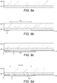
Figures 5a to 5g schematically depict components of a security device at various stages of manufacture; -
Figures 6a to 6d schematically depict components of a further security device at various stages of manufacture, the device comprising a colour tinted layer applied as a patterned screen; -
Figures 7a to 7d schematically depict components of a further security device at various stages of manufacture, wherein the steps of forming the relief structure and applying the reflection enhancing material are reversed compared to the method ofFigures 5a to 5g ; -
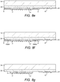
Figures 8a to 8j schematically depict components of a further security device at various stages of manufacture; -
Figures 9a to 9k schematically depict components of a further security device at various stages of manufacture; -
Figure 10 is a plan view of a security article comprising at least two holograms formed by including relief structures in at least two adjacent regions, according toFigures8j , or9k for example; -
Figures 11a and 11b depict an exemplary security document in accordance with the present invention,Figure 11b showing a cross-section along the line XX' inFigure 11a ; -
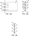
Figures 12a and 12b depict a further exemplary security document incorporating a security device in accordance with the present invention,Figure 12b being a cross-section along line XX' inFigure 12a ; -
Figures 13a, 13b and 13c depict a further exemplary security document incorporating a security device in accordance with the present invention,Figures 13b and 13c depicting alternative cross-sections of the security document taken along line XX' inFigure 13a . - The present description will focus on security documents provided with integral security devices having optically variable effect generating relief structures which give rise to diffractive optical effects, such as holograms or diffraction gratings. However, it should be appreciated that in other embodiments the relief structure may be a non-holographic micro-optical structure, such as a prismatic structure. Examples of prismatic structures suitable for the security devices of the sort presently disclosed include, but are not limited to, a series of parallel linear prisms with planar facets arranged to form a grooved surface, a ruled array of tetrahedral, an array of square pyramids, an array of corner cube structures, and an array of hexagonal faced corner cubes. Another preferred type of micro-optical structure is one which functions as a micro lens, including those that refract light at a suitably curved surface of a homogeneous material such as plano-convex lenslets, double-convex lenslets, plano-concave lenslets and double-concave lenslets. Other suitable micro-optical structures include geometric shapes based on domes, hemispheres, hexagons, squares, cones, stepped-structures, cubes or combinations thereof.
-
Figure 1 shows asecurity article 1 such as a transfer foil, security thread, patch, or similar which includes asecurity device 10 carried on asupport layer 2a (here the lower surface, facing observer B). Typically, thesupport layer 2a acts as a release sheet or strip from which thedevice 10 is detached upon application to a security document, in which case thesupport layer 2a can take any convenient form such as a (opaque, translucent or transparent) polymer or paper web. Thesupport layer 2a may be transferred with the security device onto the security document for example when the security device is applied over an aperture in the security document substrate. Alternatively, thesupport layer 2a may for example be an integral part of a security document, e.g. a polymer banknote substrate, or a layer of an identity card. If thesupport layer 2a is to remain in situ when the device is put in circulation, thesupport layer 2a should be transparent at least in regions at which the security devices are to be formed. The substrate could however be opaque in other regions, e.g. carrying one or more opacifying layers 15 definingwindow regions 11 in which the devices are to be formed, as illustrated inFigure 3 for example. - A release layer (not shown) may be provided between the
support layer 2a andsecurity device 10 to assist in the detachment of thesecurity device 10 from thesupport layer 2a upon application of thedevice 10 to a security document. For example, where the transfer is to take place by hot stamping, the release layer may comprise a release coat such as a layer of wax or similarapplied to thesupport layer 2a prior to the application of the other functional layers. - The
security device 10 comprises an at least partially translucent ortransparent substrate 2b, such as a polymer film and a colouredtinted layer 3 which is a formable material, such as an embossable lacquer. In the example ofFigure 1 , a holographic (or other optically variable)relief structure 4 is formed solely in the colour tintedlayer 3 disposed on thesubstrate 2b across a region R1. - In the example of
Figure 2 , therelief structure 4 formed within the colour tintedlayer 3 as well as theunderlying substrate 2b which is also made of an appropriate formable material, typically a thermal embossing lacquer. Thesupport layer 2a may also be formable and comprise for example a thermoplastic layer such as polyesterpolyethylene teraphthalate (PET), polyethylene, polyamide, polycarbonate, poly(vinylchloride) (PVC), poly(vinylidenechloride) (PVdC), polymethylmethacrylate (PMMA), polyethylene naphthalate (PEN), polystyrene, or polysulphone; or an embossing lacquer layer, such as a PMMA-based resin.. The device requires at least one formable layer (2a or 2b) which is not subsequently released as will be explained below in more detail. In other words, it is possible to provide a single formable support layer (e.g. 2a) without an additional formable layer (e.g. 2b). It will also be appreciated that forming the relief in theunderlying substrate 2b (orsupport layer 2a) is dependent on the thickness of the colour tintedlayer 3. The colour tinted layer 3 (and optionally thesubstrate 2b, as shown inFigure 2 ) can be formed of any suitable material in which arelief structure 4 can be formed, for example a conventional embossing lacquer such as a thermoplastic polymer or a radiation curable resin. The colourtinted layer 3 includes a colorant such as a suitable dye which imparts a tint to thelayer 3. The tint may or may not be visible to the human eye under illumination at visible wavelengths. For example, the colorant could be invisible unless irradiated with selected wavelengths outside the visible spectrum, such as UV or IR, and could be phosphorescent, fluorescent or luminescent. However, in the most preferred examples, the colorant is visible under ambient lighting conditions in order that the colour effect is readily apparent without the need for specialist equipment. - The
relief structure 4 is formed into the colour tintedlayer 3 inFigure 1 (as well as in thesubstrate 2b inFigure 2 , depending on the thickness of the colour tinted layer) using an appropriate conventional technique such as embossing under the combined action of heat and pressure, or cast curing, in which the colour tintedlayer 3 is coated as a relatively fluid resin onto thesupport layer 2a and a shaped die applied to the fluid resin having the desired relief shape. The resin flows to accommodate the die thereby taking on the desired relief shape and is simultaneously or subsequently hardened, e.g. by curing with radiation such as UV. The colourtinted layer 3 typically comprises a single homogenous film of resin. Aformable substrate 2b may comprise multiple layers including at least a protective coating layer (commonly termed a "scuff layer) which will cover the hologram in use and an embossing layer which is usually of a material which is mechanically softer and/or of lower glass transition temperature than the protective layer. Typically, aformable substrate 2b is between 1 and 5 microns thick, preferably between 1 and 3 microns thick. - The colour
tinted layer 3 carries areflection enhancing material 5 such as a metal film (e.g. aluminium or copper). The colourtinted layer 3 has been formed so as to follow the contours ofsurface relief 4 defining an optically variable effect generating structure such as a hologram or diffraction grating (as discussed further above), and thereflection enhancing material 5 follows the contours of the relief. - The colour
tinted layer 3 andreflection enhancing material 5 are substantially in register with one another (in region R1=R3) and any other layers such that their relative locations do not vary substantially between one banknote and another of the same type for example. For instance, the position tolerance of the colour tintedlayer 3 andreflection enhancing material 5 and any other layers may be as low as +/- 100 to 200 microns or exceptionally less from one document to the next. - Optionally, the reflection enhancing material may be covered with a protective coating (not shown) which may optionally contain a security substance (e.g. a fluorescent, luminescent or phosphorescent material).
- The
security device 10 is visible from both sides of thesecurity article 1 as illustrated by observers A and B.Figure 3 shows a plan view of the security document ofFigure 1 as viewed by observer B. Thedocument 1 has awindow 11 inside which thesecurity device 10 extends across the region R3 which here has the form of a sun-shaped symbol. In other cases, the region R3 may define an alternative indicia such as a letter, number or graphic, and the region R3 could extend to cover the whole window 11 (although this is less preferred). As viewed by observer B, the sun-shaped symbol has a metallic appearance, which is dictated by thereflection enhancing material 5. - From the opposite side of the
security document 1, observer A sees the same optically variable effect although the content of the hologram will appear reversed (i.e. a mirror image of that seen from the position of observer B) due to the fact that the reverse side ofrelief 4 is being viewed. However, the colour of the optically variable effect and the device as a whole will appear different from that seen from position B since it will be determined by the colour tinted layer 3 (which is at least semi-transparent) in combination with the reflection enhancing layer 5.i.e a coloured metallic appearance will be observed from position A where the colour is determined by the tint in the formable material. Thus, two different optically variable appearances can be observed from the two sides of the device. The result is therefore a particularly effective security device since the impression is given of there being two security devices of different colour in exact register with one another. This would be extremely difficult to imitate utilising two devices since the necessary level of registration would not be obtainable. As a result, the security level is significantly enhanced. - A preferred method for manufacturing a security device such as that shown in
Figure 1 will now be discussed with reference toFigures 4 and5a to 5g .Figure 4 is a flowchart depicting selected steps of the method.Figures 5a to 5g depict a security device made according to the described method, at various stages of production for cross reference withFigure 4 . - In the first step S101, a
pattern defining substance 6 is applied to a first surface of a first transparent layer, in this case represented by anembossable substrate 2b on atransparent carrier 2a as shown inFigures 5a and 5b . Thepattern defining substance 6 is laid down across areas of the substrate in which the colour tintedlayer 3 is ultimately not desired, in this case outside of region R1 as shown inFigure 5b . Thepattern defining substance 6 can comprise any material which impedes adhesion of the colour tinted layer 3 (typically an embossable resin lacquer) to theunderlying substrate 2b (and any overlying layers such as areflection enhancing material 5 in this example). In a preferred embodiment, thepattern defining substance 6 comprises a soluble mask, such as soluble ink. One exemplary type of soluble ink is heavily pigmented ink as disclosed inWO-A-99-13157 layer 3 from the substrate in the regions where the soluble mask is present. Further examples of suitable soluble masks are given inUS-A-5142383 ,US-A-3935334 andEP-A-1023499 . - With the
pattern defining substance 6 in place, in step S102, colourtinted material 3 is deposited onto thefirst surface 2a of the substrate 2 to form a layer of colour tintedmaterial 3 which extends over the window R1 defined by thepattern defining substance 6 and neighbouring regions of the substrate, including portions covered bypattern defining substance 6 as shown inFigure 5c . The colourtinted layer 3 is applied in region R2, which second overlaps at least in part the first region R1 in order that the colour tintedlayer 3 can be deposited onto and strongly bond to at least part of thesubstrate 2b. The overlapping portions of the first and second regions R1, R2 define a third region R3 in which ultimately the formedrelief structure 4 is present. The third region R3 in which the relief structure is formed may be coincident with the first region R1, but this is not essential. - In cases where the pattern defining substance comprises a soluble mask dissolvable in a solvent such as water, the colour tinted
layer 3 should be permeable to the solvent. The colourtinted layer 3 may be applied as a continuous coating layer as shown inFigure 5b or may be printed in distinct regions. In some embodiments, as shown inFigures 6b to 6d , the colour tinted material is applied in a patternedscreen 30. The region of thesubstrate 2b onto which colour tintedlayer 3 is applied (i.e. the overlapping parts of regions R1 and R2, termed the third region, R3) exhibits the desired optically variable effect. - At step S103, an optically variable effect generating
relief structure 4 is formed in the surface of the colour tintedlayer 3 as shown inFigure 5d . Optionally, therelief structure 4 may additionally be formed into the underlyingformable substrate 2b depending on the thickness of the colour tinted layer 3 (an example of which was shown inFigure 2 ). Therelief structure 4 may be formed through a conventional embossing process, e.g. involving forming the surface relief 4 (by impressing a cylindrical image forming die (e.g. an embossing roller) into athermoplastic layer 3 through the combined action of heat and pressure. Alternatively, the colour tintedlayer 3 could be an embossable lacquer or a cast cure resin. For example, thelayer 3 may be applied as a viscous liquid coating or film of monomer which is contacted by an image forming die or roller. Thesurface relief 4 is cast into the film by the simultaneous or near simultaneous exposure of thelayer 3 to radiation (e.g. UV radiation), causing polymerisation. Thesurface relief 4 is thus set into thelayer 3. UV curable polymers employing free radical or cationic UV polymerisation are suitable for the UV casting process. Examples of free radical systems include photo-crosslinkable acrylate-methacrylate or aromatic vinyl oligomeric resins. Examples of cationic systems include cycloaliphatic epoxides. Hybrid polymer systems can also be employed combining both free radical and cationic UV polymerization. Cast cure processes such as this are particularly preferred where the colour tintedlayer 3 has a relatively low glass transition or softening temperature, e.g. biaxially orientated polypropylene (BOPP) which softens at temperatures around 85°C. Structures embossed into such materials may be vulnerable to damage should the device encounter high temperatures during circulation. - In the next step S104, a reflection enhancing material is applied to the
relief 4 to form a reflection enhancing layer 5 (Figure 5e ). Thereflection enhancing layer 5 conforms to thesurface relief 4 and this is replicated in the reflection enhancing layer's opposite side, thus rendering the optically variable effect visible from both sides of the device (layer 3 being transparent or semi-transparent). In order to achieve good conformity, the thickness t1 of thereflection enhancing layer 5 is preferably less, more preferably substantially less, than the profile depth d of therelief profile 4. For instance, therelief 4 may have a profile depth d of between 50 and 500 nm, whilst thereflective layer 5 may have a thickness of between 10 and 100 nm, preferably 10 to 30 nm. In some cases the thickness of the reflection enhancing layer may be kept very thin, e.g. 5 to 10 nm, in order to render it semi-transparent. This provides for the possibility of a further colour effect whereby the apparent colour of the device changes when viewed from the same side in reflected as compared to transmitted light. - In an alternative embodiment as will be described with reference to
Figures 7a to 7d , the order of steps S103 (forming the relief structure) and S104 (applying the reflection enhancing material) may be reversed. In other words, the colour tintedlayer 3 may be embossed prior to or after depositing thereflection enhancing material 5. - In order to obtain bright holographic replay, the
reflection enhancing layer 5 is preferably a metal layer formed of one or more metals and/or alloys, e.g. aluminium, copper, nickel and/or chrome (or any alloy thereof). If desired, two or more metals or alloys could be laid down in a pattern of different regions to collectively form thelayer 5, as described inEP-A-1294576 . In other cases, the reflection enhancing material could comprise an optical interference thin film structure, a layer containing metallic particles, optically variable particles or optically variable magnetic particles, a photonic crystal layer, or a liquid crystal layer. Materials of this sort not only provide the requisite reflective properties but may impart an additional optical effect to the device, e.g. exhibiting different colours depending on the angle of view. For example, the reflection enhancing layer could comprise a multilayer structure of alternating high and low refractive index dielectric layers resulting in an optical interference structure which exhibits different colours when viewed in reflection as compared with when viewed in transmission. - The reflection enhancing material(s) could be laid down by any appropriate technique but vacuum deposition is preferred. It should be noted that whilst typically the
reflection enhancing layer 5 will be applied directly to the first colour tintedlayer 3 and therefore will be in contact with the surface of the element in which therelief structure 4 is formed, thereflection enhancing layer 5 could be spaced from that element by an intermediate transparent layer or the like, provided that the intermediate layer is sufficiently thin so that the reflection enhancing layer again follows the surface relief contour. - Depending on the nature of
pattern defining substance 6, the colour tinted layer 3 (and any overlaying reflection enhancing material 5) may not settle on thepattern defining substance 6. In other cases, some residualembossable lacquer 3 and residualreflection enhancing material 5 may remain on thepattern defining substance 6 in which case a removal step, such as washing step S105 (andFigure 5f ), may be performed. This may involve for example washing the surface ofsubstrate 2b with a liquid (e.g. water) or a gaseous substance, such as an air jet. Alternatively, a mechanical action such as vibration may be used as the removal step. Where a liquid is used, preferably the liquid has the capacity to dissolve the pattern defining substance (e.g. the soluble mask is soluble within the washing liquid) and the colour tintedlayer 3 is permeable to the liquid to allow it to reach thepattern defining substance 6 underneath it. - This causes detachment of the colour tinted
layer 3 and overlayingreflection enhancing material 5 from thesubstrate 2b in the areas wherepattern defining substance 6 is present, resulting in the same final structure shown inFigure 5g . The region of the remaining colour tintedlayer 3 to which thereflection enhancing material 5 is applied (i.e. the overlapping parts of regions R1 and R2, termed the third region, R3) exhibits the desired optically variable effect. -
Figures 6a to 6d schematically depict a variation of a method according to the invention wherein a security device 10' is formed using the same technique as described above, except a patterned screen of colour tintedmaterial 30 is applied instead of acontinuous layer 3 as described with reference toFigures 5c to 5g above. Advantageously, using ascreen 30 enhances permeability of the colour tinted layer. The method steps ofFigures 6a to 6d is the same as that described with theFigures 5a to 5g , the detailed description of which is not repeated here. The patterned screen of colour tintedmaterial 30 in this example is a thin screen of colour tinted material with a typical thickness of 0.5 to 5 microns, preferably 0.5 to 2 microns. The width of the lines or the diameter of the dots forming thescreen 30 are preferably in the range 20-200 microns and the spaces between the dots or lines are also in the range 20-200 microns. Accordingly, the dimensions of thescreen 30 are such that it is not readily observable with the naked eye. Thereflection enhancing material 50 is applied over thescreen 30 in a similar manner as indicated above. -
Figures 7a to 7d schematically depict components of afurther security device 10" at various stages of manufacture, wherein the steps of forming the relief structure (S103) and applying the reflection enhancing material (S104) are reversed compared to the method ofFigures 5a to 5g described above. In this example, thesubstrate 2b is a formable (e.g. embossable) layer as described above in regions R1=R3 and anadditional relief structure 40 is provided in at least one adjacent region R4 not comprising the colour tintedlayer 3, as shown inFigure 7d . In this example, therelief structures Figure 7d ), for example with a die carrying the relief structure, wherein the die advantageously forms part of an embossing roller. The device as shown inFigure 7d is not preferrable as there is no reflection enhancing layer associated withrelief structure 40 therefore the optically variable effect generated by the relief structure will not be readily apparent. A further metallised layer may be added to 40 as a later step or the same process may be applied, as shown inFigures 8a-8g , so that both relief structures have a metallised layer. - The result is a security device as described above with an additional, adjacent, region displaying an optically variable effect to the observers. If
substrate 2b is clear and colourless, the optically variable effect in region R4 will be the same for both observers A and B. Advantageously, thesecurity device 10" may displays a central region R1=R3 (e.g. with a colour tint as viewed by observer A and a metallic appearance as viewed by observer B) in register with adjacent regions R4 exhibiting the same effect from either view point A or B. Accordingly, the security of the device is increased since such an effect is difficult to reproduce by counterfeiters. -
Figures 8a to 8j schematically depict components of a further security device 10'" at various stages of manufacture.Figures 8a to 8c respectively illustrate the same method steps asFigures 5a to 5c described above. In this example, thesubstrate 2b is a formable (e.g. embossable) layer as described above. InFigure 8d , in addition to forming arelief structure 41 in region (R1=R3) comprising the colour tintedlayer 3, at least afurther relief structure 42 is formed in an adjacent region R5 not comprising the colour tinted layer. In this example, therelief structures Figure 8d ), for example by embossingstructures structures - Next, as shown in
Figure 8e , areflection enhancing layer 52 is applied to thesubstrate 2b as described above with reference to step S104, covering region (R1=R3) comprising the colour tintedlayer 3, as well as the at least one adjacent region R5 not comprising the colour tinted layer. Following the formation of therelief structure 41, areflection enhancing layer 52 such as a metal is applied, preferably by vacuum metallisation (as described above with reference to S104 ofFigure 4 for example). Thereflection enhancing layer 52 respectively conforms to therelief structures Figure 8e , the metallisation covers the full area of thedevice 10"'. -
Figures 8f and 8g depict the removal of residual colourtinted layer 3 and any overlaying residual refection enhancing material in region (R1=R3) as described above (with reference to step S105 ofFigure 4 for example). Further, as shown inFigure 8h asecond layer 22 which is at least partially translucent or transparent is preferably printed over thedevice 10 in region (R1=R3) (left hand side of the device). Thelayer 22 may in practice be formed of multiple layers laminated to one another, and this applies to all "layers" mentioned throughout this disclosure. In this example, thesecond layer 22 is a clear alkali resistant mask printed in register with the coloured lacquer 3 (with a register tolerance achievable by normal printing techniques i.e. +/- 100 microns). The thickness of the secondtransparent layer 22 is 0.5-5 microns and preferably 1-2 microns. Most preferably, thematerial forming layer 22 is suitable for acting as a etch resist, with thelayer 22 protecting thereflection enhancing layer 52 during a subsequent etching step shown inFigure 8j , in which those regions of thereflection enhancing layer 52 which are not covered by thethird layer 24 are removed. - Further, as shown
Figure 8i , athird layer 24 which is at least partially translucent or transparent is applied over the reflection enhancing layer 23 across a region R5 (right hand side of the device). Thethird layer 24 is preferably laid down in the form of a decorative or secure shape or pattern, such as letters, numbers, symbols or other indicia, or a shape or fine line pattern. As in the previous examples, it is preferable that the shape or pattern includes at least two visibly discontinuous regions - i.e. areas of the pattern which are sufficiently large and spaced by a sufficient distance that they can be individually distinguished by the naked eye. This increases the complexity and visual impact of the design. Within each such region (which appears continuous and unbroken, to the naked eye), thethird layer 24 can be applied in a contiguous, all-over layer, or could be applied as a screened working - that is, an array of spaced screen elements. The dimensions of such a screen are typically sufficiently small that the elements cannot be individually distinguished by the naked eye, and the region appears as if the layer is continuous. Nonetheless, this can be used to make the device semi-transparent since light can be transmitted through the screen. - Similar materials may be used for
layers Layer 22 in region R1 may be colour tinted but preferably it is not to contrast with the colour oflayer 24 region R5. As shown inFigures 8h-8j , layers 22 and 24 do not follow the relief structure at the outermost surface i.e. the outer surface is flat. - In order to achieve a high degree of control over the arrangement of the
third layer 24, the material is preferably laid down using a printing technique such as gravure printing. However, other application techniques such as coating, deposition or transfer methods could be used as appropriate. In this example, thethird layer 24 includes an optically effective substance such as a colorant typically in the form of a dye or pigment (a dye is preferred in order to preserve the optical clarity of the layer). Various different types of colorant may be used which may or may not be visible to the human eye under normal illumination conditions. For example, the colorant could be visible or detectable only under selected non-visible radiation wavelength such as ultraviolet or infrared. However, in the most preferred embodiments, the colorant is visible under ambient white light and imparts a coloured tint to thelayer 24, e.g. red, blue, green etc. - If desired, a multi-coloured arrangement of transparent materials containing different colorants could be used to form the
layer 24. For example, one half of thelayer 24 may appear red, whilst the other laterally offset half may appear blue, resulting in a visible pattern. In some cases, theentire layer 24 may have the same visible colour, with selected portions thereof additionally carrying a UV or IR active substance. The different colours could be arranged in any desired pattern, e.g. defining indicia, or different colours could be used to highlight different regions of the optically variable area. Some individual areas oflayer 24 could contain no optically effective substance. Patterned arrangements such as this can be achieved by laying down two or more transparent materials, at least one containing an optically effective substance, in registration with one another in accordance with the desired design, e.g. by printing. - Any of the optically effective substances may if desired be responsive to nonoptical stimuli such as temperature, pressure, strain, electrical potential or any combination thereof. For instance, the substance could be thermochromic, piezochromic or electrochromic, undergoing a change in appearance as the relevant parameter changes. In this case, the optically effective substance may only be visible or detectable under certain stimulus conditions (e.g. within a certain temperature range).
- The colorant or other optically effective substance is dispersed within a clear material to make up
layer 24, such as a polymeric binder or resin. Suitable examples include vinyl resins such as UCAR™ VMCA Solution Vinyl Resin or UCAR™ VCMH Solution Vinyl Resin, both of which are supplied by The Dow Chemical Company and which are carboxy-functional terpolymers comprised of vinyl chloride, vinyl acetate and maleic acid. Most preferably, thematerial forming layer 24 is suitable for acting as a etch resist, with thelayer 24 protecting thereflection enhancing layer 52 during a subsequent etching step shown inFigure 8j , in which those regions of thereflection enhancing layer 52 which are not covered by thethird layer 24 are removed. Where thereflection enhancing layer 52 is a metal, typically this removal step is achieved by immersing the structure in an etchant solution which dissolves or otherwise removes the uncovered metal. For example, where the reflection enhancing layer is aluminium, sodium hydroxide can be used as the etchant. Where the reflective layer is copper, an acidic etchant is typically used, such as (i) a mixture ofHydrochloric acid 50%v and Ferric chloride (40 Baume) 50%v, at room temperature; or (ii) a mixture of Sulphuric acid (66 Baume) 5-10%v and Ferrous sulphate 100g/litre, at 40 to 60 degrees C. Other etchants may also be used such as nitric acid but generally the above systems are the most convenient to work with. The exemplary materials mentioned above for forming the third transparent layer 24 (UCAR™ VMCA and UCAR™ VMCH) are suitable etch resists for both of these etch systems. In order to fully protect thereflection enhancing layer 52, the thirdtransparent layer 24 preferably has a thickness of tz the order of 0.5 to 5 microns, more preferably 1 to 2 microns. However, the thickness required will depend on the selected materials and etchant. - Other techniques such as laser ablation or (reactive) ion etching could be used to remove the uncovered material of the
reflection enhancing layer 52 and these may be particularly preferred where the layer is not solely a metal or alloy layer, such as metallic ink or an interference layer structure as mentioned above. In each case the second transparent layer would still be used to define the bounds of the area in which the layer is removed. Where thereflection enhancing layer 52 is an interference thin film structure (e.g. metal/dielectric/metal), etching techniques may be used for removal in the same manner as a metal reflective layer. In this case, not all the layers of the interference thin film structure may be removed by the etching. - Advantageously, the resulting device 10'" of
Figure 8j viewed by observer A may therefore display a first, coloured, holographic region (left hand side, R1=R3), as dictated by the colour of the colour tintedlayer 3, in register with a metallic holographic region (right hand side, R5). On the reverse side, when viewed by observed B, the device 10'" presents a second coloured holographic region (right hand side, R5), as dictated by the colour of thethird layer 24, in register with a metallic holographic region (left hand side, R1=R3). This further increases the security of the device since such an effect is difficult to reproduce by counterfeiters. - The method depicted by
Figures 9a to 9k depicts an alternative method to the method ofFigures 8a to 8j described above for producing adevice 10"" with optical effects displayed in front and back colours in register with opposing metallic regions. The steps ofFigures 9a, 9b, 9c respectively correspond to those of steps 5a, 5b, 5c and 8a,8b,8c described above. The method depicted inFigures 9a to 9k differs from the method ofFigures 8a to 8j in that the first andsecond relief structures 43, 44 (on the left and right hand side of the device respectively) are formed in separate relief forming stages, inFigures 9d and9h , respectively. In the example ofFigures 8a to 8j , thesecond relief structure 42 is formed intolayer 2b and athird layer 24, typically an alkali resist layer, is subsequently applied and serves to protect thereflection enhancing material 52 from being removed (e.g. etched) by a second removal step (i.e. demetallisation) as described with reference toFigure 8j . - As shown in
Figure 9g , the second layer 22' (which is at least partially translucent or transparent) is applied throughout all regions of thedevice 10‴. In this example, layer 22' is a thermoformable layer (rather than an alkali resist layer as described with reference toFigures 8h to 8j above). The thermoformable layer 22' can be formed with a second relief structure 44 (Figure 9h ) at temperature and pressure sufficiently below that of the colouredtinted layer 3, that therelief 43 previously formed into the colouredtinted layer 3 is not degraded. - Preferably, a post cure process applied (
Figure 9h ) to either the colouredtinted layer 3 after forming thesecond relief structure 44 the thus elevating its softening temperature to a value where it is not impacted by the first forming of the relief structure 43 (i.e. first embossing phase inFigure 9e ). Alternatively, a post cure process may be applied after forming the second relief structure 44 (i.e. the embossing of the layer 22') such that in its pre cure phase it has a much lower softening temperature than the colour tintedlayer 3 and can be 'soft embossed' and then cured to a more durable state. - A UV curable layer 22' may be applied as a viscous liquid coating or film of monomer which is contacted by an image forming die or roller. The surface relief is cast into the film by the simultaneous or near simultaneous exposure of the layer 22' to radiation (e.g. UV radiation), causing polymerisation. UV curable polymers employing free radical or cationic UV polymerisation are suitable for the UV casting process. Examples of free radical systems include photo-crosslinkable acrylate-methacrylate or aromatic vinyl oligomeric resins. Examples of cationic systems include cycloaliphatic epoxides. Hybrid polymer systems can also be employed combining both free radical and cationic UV polymerization. Cast cure processes such as this are particularly preferred where the substrate has a relatively low glass transition or softening temperature, e.g. biaxially orientated polypropylene (BOPP) which softens at temperatures around 85°C. Structures embossed into such materials may be vulnerable to damage should the device encounter high temperatures during circulation.
- As shown in
Figure 9i , a secondreflection enhancing layer 5 is applied, preferably by vacuum metallisation as described above. It will be appreciated that the secondreflection enhancing layer 5 may comprise a metal which is may different than the metal applied in the previous step metallisation step (ofFigure 9e ). The secondreflection enhancing layer 5 follows therelief structure 44 and is typically 10-30 nm thick. -
Figure 9j , afurther layer 26 which is transparent or semi-transparent is applied to protect the reflection enhancing layer 53 aboverelief structure 44. As withlayer 24 described with reference toFigures 8i and 8j ,layer 26 is suitable for acting as an etch resist, protecting the second reflection enhancing layer 5 (applied in the step ofFigure 9i ) during a subsequent etching step shown inFigure 9k , in which those regions of thereflection enhancing layer 5 which are not covered bylayer 26 are removed. Preferably,layer 26 is tinted with a colour different to the colour of the formable material applied previously (in the step ofFigure 9c ) so that the device advantageously displays different colours on the left hand side of the device compared to the right hand side. The thickness oflayer 26 is 0.5-5 microns and preferably 1-2 microns. -
Figure 10 is a plan view of a security article 1' comprising at least two holograms formed by including relief structures in at least two regions, according toFigures 8j or9k described above. The device has multiple regions (R1=R3) displaying a metallic silver appearance to an observer B due to an applied Al layer representing a reflection enhancing material described above. To an observer A, regions R1=R3 appear metallic yellow due to the formable material in regions being yellow tinted in this example. The device has an additional region R4 or R5 as referred to above according toFigures 8j or9k which appear metallic silver (due to the Al layer) from viewpoint A and purple, for example, fromviewpoint B. Numeral 50 indicates a region where there is no metal is formed by patterning of the metallisation layer in region R4 or R5. For example, in the method described with reference toFigure 8 , apattern defining substance 6 may be applied in the shape indicated byshape 50 in the middle of region R4. Alternatively, in the method described with reference toFigure 9 ,shape 50 may be achieve by patterning the coloured resistlayer 26 in region R5. -
Figures 11, 12 and13 depict examples of security documents in which security devices of the sorts described above have been incorporated.Figure 11 shows a first exemplary security document, here abanknote 140, in (a) plan view and (b) cross-section along line XX'. Here, thebanknote 140 is a polymer banknote, comprising an internaltransparent polymer substrate 142 which is coated on each side withopacifying layers 143a and 143b in a conventional manner. In some cases, the opacifying layers may be provided on one side of thesubstrate 142 only. The opacifying layers 143a and 143b are omitted in a region of the document so as to define awindow 141, here having a square shape. Within thewindow region 141 is located asecurity device 120 in accordance with any of the embodiments discussed above. The outer perimeter of thedevice 120 is denoted by the dashed circular line surrounding the "sun shaped" optically variable effect region. Thesecurity device 120 may be formed integrally in thebanknote 140 with the relief structure 122 being formed directly in the surface oftransparent substrate 142. Alternatively, thesecurity device 120 may have been formed separately as a security article such as a transfer patch or label.. In this case, thesecurity device 120 may be affixed to thetransparent substrate 142 inside thewindow region 141 by means of the transparent adhesive 125. Application may be achieved by a hot or cold transfer method e.g. hot stamping. - It should be noted that a similar construction could be achieved using a paper/plastic composite banknote in which the
opacifying layers 143a and 143b are replaced by paper layers laminated (with or without adhesive) to an internaltransparent polymer layer 142. The paper layers may be omitted from the window region from the outset, or the paper could be removed locally after lamination. In other constructions, the order of the layers may be reversed with a (windowed) paper layer on the inside and transparent polymer layers on the outside. - In
Figure 12 , thebanknote 140 is of conventional construction having asubstrate 144 formed for example of paper or other relatively opaque or translucent material. Thewindow region 41 is formed as an aperture through thesubstrate 144. Thesecurity device 120 is applied as a patch overlapping the edges ofwindow 141 utilising transparent adhesive 125 to join the security article to thedocument substrate 144. Again, the application of the security device and document could be achieved using various methods including hot stamping. -
Figure 13 depicts a third example of a security document, again abanknote 140, to which asecurity article 150 in the form of a security thread or security strip has been applied. Threesecurity devices 20 each carried on thestrip 150 are revealed throughwindows 141, arranged in a line on thedocument 140. Two alternative constructions of the document are shown in cross-section inFigures 13b and 13c. Figure 13b depicts the security thread orstrip 150 incorporated within thesecurity document 140. For example, the security thread orstrip 50 may be incorporated within the substrate's structure during the paper making process using well known techniques. To form thewindows 141, the paper may be removed locally after completion of the paper making process, e.g. by abrasion. Alternatively, the paper making process could be designed so as to omit paper in the desired window regions.Figure 13c shows an alternative arrangement in which the security thread orstrip 150 carrying thesecurity device 120 is applied to one side of document substrate 145, e.g. using adhesive. Thewindows 141 are formed by provision of apertures in the substrate 145, which may exist prior to the application ofstrip 150 or be formed afterwards, again for example by abrasion. - Many alternative techniques for incorporating security documents of the sorts discussed above are known and could be used. For example, the above described device structures could be formed directly on other types of security document including identification cards, driving licenses, bankcards and other laminate structures, in which case the security device may be incorporated directly within the multilayer structure of the document.
Claims (15)
- A method of manufacturing a security device (10), comprising:(a) providing a first layer (2b) comprising at least a partially translucent or transparent region;(b) applying (S101) pattern defining substance (6) on a surface of the first transparent layer, excluding at least one first region (R1) on the surface of the first layer aligned with the at least a partially translucent or transparent region;(c) applying (S102) a formable material (3) to a second region (R2) of the first surface, wherein the second region overlaps at least part of the at least one first region, the overlapping portions of the first and second regions respectively defining at least one third region (R3);
then performing the steps (d) and (e) in any order:(d) forming (S103) the formable material in the at least one third region such that its surface distal from the first layer follows the contours of a first optically variable effect generating relief structure (4) in the at least one first region; and(e) applying (S104) a first reflection enhancing material (5) over the formable material to form a reflection enhancing layer which follows the contour of the relief structure;
wherein the pattern defining substance impedes the retention, in areas to which the pattern defining substance was applied, of the formable material and any overlaying reflection enhancing material. - A method according to claim 1, further comprising, after step (e), the step of:
(f) removing the formable material (3) and any reflection enhancing material (5) overlaying the formable material from regions of the device in which the pattern defining substance was applied. - A method according to claim 1 or claim 2, wherein the pattern defining substance (6) comprises a soluble mask which can be dissolved by application of a solvent, thereby impeding adhesion of the formable material to the first layer.
- A method according to claim 3, wherein the formable material (3) comprises a material permeable to the solvent.
- A method according to any preceding claim, wherein in step (c), the formable material (3) is applied in a pattern to form a screen.
- A method according to any of the preceding claims, wherein in steps (b), (c), and/or (e), the respective pattern defining substance (6), formable material (3), and first reflection enhancing layer (5) are applied in register with one another and preferably in register with the relief structure (4) formed in step (d).
- A method according to any of any of the preceding claims, wherein the formable material (3) comprises one or more optically effective substance(s) which impart to the formable material a visible coloured tint of a first colour.
- A method according to any of the preceding claims, wherein, in step (e), the reflection enhancing material (5) is applied in a continuous layer over the relief structure.
- A method according to any of the preceding claims, wherein the first reflection enhancing material (5) comprises any of:• one or more metals or alloys thereof preferably copper and/or aluminium;• an optical interference thin film structure;• a layer containing metallic particles, optically variable particles or optically variable magnetic particles;• a photonic crystal layer; or• a liquid crystal layer.
- A method according to any of the preceding claims, wherein the first (R1) and/or third (R3) regions define respective indicia such as a character, number, letter, alphanumerical text, symbol, graphic element or the like, preferably being different.
- A method according to any of the preceding claims, wherein the first layer (2b) is a formable layer and wherein in step (d), forming the formable material (3) comprises forming, in the at least one third region, the surface of the underlying first layer to which the formable material is applied, such that it follows, at least in part, the contours of the first optically variable effect generating relief structure (4), wherein step (d) further comprises forming the surface of the first layer in at least one fourth region (R4) separate from the at least one third region and in which the formable material is not applied, such that it follows the contours of a second optically variable effect generating relief structure.
- A method according to claim 11, further comprising the steps of:
(f1) removing the formable material (3) and any residual reflection enhancing material overlaying the formable material in areas in which the pattern defining substance (6) was applied;providing, in register with the retained formable material, a second layer which is at least partially translucent or transparent; andproviding, in register with the second relief structure, a third layer (24) which is at least partially translucent or transparent, wherein the third layer comprises one or more optically effective substances which impart a coloured tint to the third layer, which colour is preferably different from the colour of the formable material. - A method according to any of claims 1 to 11, further comprising the steps of:
(f2) removing the formable material and any residual reflection enhancing material overlaying the formable material in areas in which the pattern defining substance (6) was applied;applying a fourth layer comprising a thermoplastic polymer or a curable polymer, preferably a UV-curable polymer, the fourth layer being at least partially translucent or transparent;forming the surface of the first layer (2b) in a fifth region separate from the third region on the surface of the first layer aligned with the at least a partially translucent or transparent region and in which the formable material (3) is not applied, such that it follows the contours of a third optically variable effect generating relief structure;applying a second reflection enhancing material (5) over the fourth layer to form a reflection enhancing layer which follows the contours of the third relief structure; andproviding, in register with the third relief structure, a fifth layer which is at least a partially translucent or transparent, wherein the fifth layer comprises one or more optically effective substances which impart a coloured tint to the fifth transparent layer, which colour is preferably different from the colour of the formable material (3). - A security device (10) made in accordance with any of the preceding claims.
- A security document (1) comprising a security device (10) according to claim 14 wherein the security device is formed in a window (11) of a polymer or paper substrate.
Applications Claiming Priority (2)
| Application Number | Priority Date | Filing Date | Title |
|---|---|---|---|
| GB1606723.3A GB2549481B (en) | 2016-04-18 | 2016-04-18 | Security devices and methods of manufacture thereof |
| PCT/GB2017/051075 WO2017182792A1 (en) | 2016-04-18 | 2017-04-18 | Security devices and methods of manufacture thereof |
Publications (2)
| Publication Number | Publication Date |
|---|---|
| EP3445592A1 EP3445592A1 (en) | 2019-02-27 |
| EP3445592B1 true EP3445592B1 (en) | 2021-11-10 |
Family
ID=58633034
Family Applications (1)
| Application Number | Title | Priority Date | Filing Date |
|---|---|---|---|
| EP17719686.2A Active EP3445592B1 (en) | 2016-04-18 | 2017-04-18 | Security devices and methods of manufacture thereof |
Country Status (3)
| Country | Link |
|---|---|
| EP (1) | EP3445592B1 (en) |
| GB (1) | GB2549481B (en) |
| WO (1) | WO2017182792A1 (en) |
Cited By (1)
| Publication number | Priority date | Publication date | Assignee | Title |
|---|---|---|---|---|
| US11945253B2 (en) | 2019-05-20 | 2024-04-02 | Crane & Co., Inc. | Use of nanoparticles to tune index of refraction of layers of a polymeric matrix to optimize microoptic (MO) focus |
Families Citing this family (7)
| Publication number | Priority date | Publication date | Assignee | Title |
|---|---|---|---|---|
| CN111716939B (en) * | 2019-03-19 | 2021-10-26 | 中钞特种防伪科技有限公司 | Optical anti-counterfeiting element and optical anti-counterfeiting product |
| CN111716936B (en) * | 2019-03-19 | 2021-08-06 | 中钞特种防伪科技有限公司 | Optical anti-counterfeiting element and optical anti-counterfeiting product |
| CN111716937B (en) * | 2019-03-19 | 2021-10-26 | 中钞特种防伪科技有限公司 | Optical anti-counterfeiting element and optical anti-counterfeiting product |
| CN111746172B (en) * | 2019-03-29 | 2021-11-12 | 中钞特种防伪科技有限公司 | Double-sided different-color optical anti-counterfeiting element and manufacturing method thereof |
| JP7452376B2 (en) | 2019-09-19 | 2024-03-19 | Toppanホールディングス株式会社 | Transfer foil and its manufacturing method |
| DE102020000345A1 (en) | 2020-01-17 | 2021-07-22 | Sioptica Gmbh | Process for the production of a component with a structured surface |
| EP3865312B1 (en) * | 2020-02-14 | 2023-11-08 | Hueck Folien Gesellschaft m.b.H. | Method for manufacturing a safety element |
Family Cites Families (5)
| Publication number | Priority date | Publication date | Assignee | Title |
|---|---|---|---|---|
| DE102007055112A1 (en) * | 2007-01-05 | 2008-07-10 | Giesecke & Devrient Gmbh | Producing safety foil for valuable document e.g. check, comprises printing a side of substrate with a printing ink in the form of characters to be produced, applying a coating on the printed side and removing the printing ink |
| JP6476863B2 (en) * | 2012-11-19 | 2019-03-06 | 凸版印刷株式会社 | Anti-counterfeit structure and manufacturing method thereof |
| GB2514337B (en) * | 2013-05-17 | 2020-01-15 | De La Rue Int Ltd | Security documents and methods of manufacture thereof |
| GB2514338B (en) * | 2013-05-17 | 2020-06-10 | De La Rue Int Ltd | Security documents and methods of manufacture |
| WO2016206760A1 (en) * | 2015-06-26 | 2016-12-29 | Fedrigoni Spa | Security element with pattern and double-sided holographic effect |
-
2016
- 2016-04-18 GB GB1606723.3A patent/GB2549481B/en active Active
-
2017
- 2017-04-18 WO PCT/GB2017/051075 patent/WO2017182792A1/en active Application Filing
- 2017-04-18 EP EP17719686.2A patent/EP3445592B1/en active Active
Cited By (1)
| Publication number | Priority date | Publication date | Assignee | Title |
|---|---|---|---|---|
| US11945253B2 (en) | 2019-05-20 | 2024-04-02 | Crane & Co., Inc. | Use of nanoparticles to tune index of refraction of layers of a polymeric matrix to optimize microoptic (MO) focus |
Also Published As
| Publication number | Publication date |
|---|---|
| GB2549481B (en) | 2019-06-05 |
| EP3445592A1 (en) | 2019-02-27 |
| GB2549481A (en) | 2017-10-25 |
| WO2017182792A1 (en) | 2017-10-26 |
Similar Documents
| Publication | Publication Date | Title |
|---|---|---|
| EP2951029B1 (en) | Security devices and methods of manufacture thereof | |
| EP3445592B1 (en) | Security devices and methods of manufacture thereof | |
| US9902187B2 (en) | Security devices and methods of manufacture thereof | |
| US10112432B2 (en) | Security device | |
| EP2441593B1 (en) | Security element with achromatic features | |
| JP5979506B2 (en) | Security element and security element manufacturing process | |
| JP2014500811A5 (en) | ||
| JP2021514485A (en) | Security element and manufacturing method of security element | |
| CA2587039A1 (en) | A security device formed by a hologram and a color shifting ink |
Legal Events
| Date | Code | Title | Description |
|---|---|---|---|
| STAA | Information on the status of an ep patent application or granted ep patent |
Free format text: STATUS: UNKNOWN |
|
| STAA | Information on the status of an ep patent application or granted ep patent |
Free format text: STATUS: THE INTERNATIONAL PUBLICATION HAS BEEN MADE |
|
| PUAI | Public reference made under article 153(3) epc to a published international application that has entered the european phase |
Free format text: ORIGINAL CODE: 0009012 |
|
| STAA | Information on the status of an ep patent application or granted ep patent |
Free format text: STATUS: REQUEST FOR EXAMINATION WAS MADE |
|
| 17P | Request for examination filed |
Effective date: 20181017 |
|
| AK | Designated contracting states |
Kind code of ref document: A1 Designated state(s): AL AT BE BG CH CY CZ DE DK EE ES FI FR GB GR HR HU IE IS IT LI LT LU LV MC MK MT NL NO PL PT RO RS SE SI SK SM TR |
|
| AX | Request for extension of the european patent |
Extension state: BA ME |
|
| STAA | Information on the status of an ep patent application or granted ep patent |
Free format text: STATUS: REQUEST FOR EXAMINATION WAS MADE |
|
| DAV | Request for validation of the european patent (deleted) | ||
| DAX | Request for extension of the european patent (deleted) | ||
| GRAP | Despatch of communication of intention to grant a patent |
Free format text: ORIGINAL CODE: EPIDOSNIGR1 |
|
| STAA | Information on the status of an ep patent application or granted ep patent |
Free format text: STATUS: GRANT OF PATENT IS INTENDED |
|
| INTG | Intention to grant announced |
Effective date: 20210607 |
|
| GRAS | Grant fee paid |
Free format text: ORIGINAL CODE: EPIDOSNIGR3 |
|
| GRAA | (expected) grant |
Free format text: ORIGINAL CODE: 0009210 |
|
| STAA | Information on the status of an ep patent application or granted ep patent |
Free format text: STATUS: THE PATENT HAS BEEN GRANTED |
|
| AK | Designated contracting states |
Kind code of ref document: B1 Designated state(s): AL AT BE BG CH CY CZ DE DK EE ES FI FR GB GR HR HU IE IS IT LI LT LU LV MC MK MT NL NO PL PT RO RS SE SI SK SM TR |
|
| REG | Reference to a national code |
Ref country code: GB Ref legal event code: FG4D |
|
| REG | Reference to a national code |
Ref country code: AT Ref legal event code: REF Ref document number: 1445739 Country of ref document: AT Kind code of ref document: T Effective date: 20211115 Ref country code: CH Ref legal event code: EP |
|
| REG | Reference to a national code |
Ref country code: DE Ref legal event code: R096 Ref document number: 602017049074 Country of ref document: DE |
|
| REG | Reference to a national code |
Ref country code: IE Ref legal event code: FG4D |
|
| REG | Reference to a national code |
Ref country code: LT Ref legal event code: MG9D |
|
| REG | Reference to a national code |
Ref country code: NL Ref legal event code: MP Effective date: 20211110 |
|
| PG25 | Lapsed in a contracting state [announced via postgrant information from national office to epo] |
Ref country code: RS Free format text: LAPSE BECAUSE OF FAILURE TO SUBMIT A TRANSLATION OF THE DESCRIPTION OR TO PAY THE FEE WITHIN THE PRESCRIBED TIME-LIMIT Effective date: 20211110 Ref country code: LT Free format text: LAPSE BECAUSE OF FAILURE TO SUBMIT A TRANSLATION OF THE DESCRIPTION OR TO PAY THE FEE WITHIN THE PRESCRIBED TIME-LIMIT Effective date: 20211110 Ref country code: FI Free format text: LAPSE BECAUSE OF FAILURE TO SUBMIT A TRANSLATION OF THE DESCRIPTION OR TO PAY THE FEE WITHIN THE PRESCRIBED TIME-LIMIT Effective date: 20211110 Ref country code: BG Free format text: LAPSE BECAUSE OF FAILURE TO SUBMIT A TRANSLATION OF THE DESCRIPTION OR TO PAY THE FEE WITHIN THE PRESCRIBED TIME-LIMIT Effective date: 20220210 |
|
| PG25 | Lapsed in a contracting state [announced via postgrant information from national office to epo] |
Ref country code: IS Free format text: LAPSE BECAUSE OF FAILURE TO SUBMIT A TRANSLATION OF THE DESCRIPTION OR TO PAY THE FEE WITHIN THE PRESCRIBED TIME-LIMIT Effective date: 20220310 Ref country code: SE Free format text: LAPSE BECAUSE OF FAILURE TO SUBMIT A TRANSLATION OF THE DESCRIPTION OR TO PAY THE FEE WITHIN THE PRESCRIBED TIME-LIMIT Effective date: 20211110 Ref country code: PT Free format text: LAPSE BECAUSE OF FAILURE TO SUBMIT A TRANSLATION OF THE DESCRIPTION OR TO PAY THE FEE WITHIN THE PRESCRIBED TIME-LIMIT Effective date: 20220310 Ref country code: PL Free format text: LAPSE BECAUSE OF FAILURE TO SUBMIT A TRANSLATION OF THE DESCRIPTION OR TO PAY THE FEE WITHIN THE PRESCRIBED TIME-LIMIT Effective date: 20211110 Ref country code: NO Free format text: LAPSE BECAUSE OF FAILURE TO SUBMIT A TRANSLATION OF THE DESCRIPTION OR TO PAY THE FEE WITHIN THE PRESCRIBED TIME-LIMIT Effective date: 20220210 Ref country code: NL Free format text: LAPSE BECAUSE OF FAILURE TO SUBMIT A TRANSLATION OF THE DESCRIPTION OR TO PAY THE FEE WITHIN THE PRESCRIBED TIME-LIMIT Effective date: 20211110 Ref country code: LV Free format text: LAPSE BECAUSE OF FAILURE TO SUBMIT A TRANSLATION OF THE DESCRIPTION OR TO PAY THE FEE WITHIN THE PRESCRIBED TIME-LIMIT Effective date: 20211110 Ref country code: HR Free format text: LAPSE BECAUSE OF FAILURE TO SUBMIT A TRANSLATION OF THE DESCRIPTION OR TO PAY THE FEE WITHIN THE PRESCRIBED TIME-LIMIT Effective date: 20211110 Ref country code: GR Free format text: LAPSE BECAUSE OF FAILURE TO SUBMIT A TRANSLATION OF THE DESCRIPTION OR TO PAY THE FEE WITHIN THE PRESCRIBED TIME-LIMIT Effective date: 20220211 Ref country code: ES Free format text: LAPSE BECAUSE OF FAILURE TO SUBMIT A TRANSLATION OF THE DESCRIPTION OR TO PAY THE FEE WITHIN THE PRESCRIBED TIME-LIMIT Effective date: 20211110 |
|
| PG25 | Lapsed in a contracting state [announced via postgrant information from national office to epo] |
Ref country code: SM Free format text: LAPSE BECAUSE OF FAILURE TO SUBMIT A TRANSLATION OF THE DESCRIPTION OR TO PAY THE FEE WITHIN THE PRESCRIBED TIME-LIMIT Effective date: 20211110 Ref country code: SK Free format text: LAPSE BECAUSE OF FAILURE TO SUBMIT A TRANSLATION OF THE DESCRIPTION OR TO PAY THE FEE WITHIN THE PRESCRIBED TIME-LIMIT Effective date: 20211110 Ref country code: RO Free format text: LAPSE BECAUSE OF FAILURE TO SUBMIT A TRANSLATION OF THE DESCRIPTION OR TO PAY THE FEE WITHIN THE PRESCRIBED TIME-LIMIT Effective date: 20211110 Ref country code: EE Free format text: LAPSE BECAUSE OF FAILURE TO SUBMIT A TRANSLATION OF THE DESCRIPTION OR TO PAY THE FEE WITHIN THE PRESCRIBED TIME-LIMIT Effective date: 20211110 Ref country code: DK Free format text: LAPSE BECAUSE OF FAILURE TO SUBMIT A TRANSLATION OF THE DESCRIPTION OR TO PAY THE FEE WITHIN THE PRESCRIBED TIME-LIMIT Effective date: 20211110 Ref country code: CZ Free format text: LAPSE BECAUSE OF FAILURE TO SUBMIT A TRANSLATION OF THE DESCRIPTION OR TO PAY THE FEE WITHIN THE PRESCRIBED TIME-LIMIT Effective date: 20211110 |
|
| REG | Reference to a national code |
Ref country code: DE Ref legal event code: R097 Ref document number: 602017049074 Country of ref document: DE |
|
| PLBE | No opposition filed within time limit |
Free format text: ORIGINAL CODE: 0009261 |
|
| STAA | Information on the status of an ep patent application or granted ep patent |
Free format text: STATUS: NO OPPOSITION FILED WITHIN TIME LIMIT |
|
| 26N | No opposition filed |
Effective date: 20220811 |
|
| PG25 | Lapsed in a contracting state [announced via postgrant information from national office to epo] |
Ref country code: AL Free format text: LAPSE BECAUSE OF FAILURE TO SUBMIT A TRANSLATION OF THE DESCRIPTION OR TO PAY THE FEE WITHIN THE PRESCRIBED TIME-LIMIT Effective date: 20211110 |
|
| PG25 | Lapsed in a contracting state [announced via postgrant information from national office to epo] |
Ref country code: SI Free format text: LAPSE BECAUSE OF FAILURE TO SUBMIT A TRANSLATION OF THE DESCRIPTION OR TO PAY THE FEE WITHIN THE PRESCRIBED TIME-LIMIT Effective date: 20211110 |
|
| REG | Reference to a national code |
Ref country code: BE Ref legal event code: MM Effective date: 20220430 |
|
| PG25 | Lapsed in a contracting state [announced via postgrant information from national office to epo] |
Ref country code: MC Free format text: LAPSE BECAUSE OF FAILURE TO SUBMIT A TRANSLATION OF THE DESCRIPTION OR TO PAY THE FEE WITHIN THE PRESCRIBED TIME-LIMIT Effective date: 20211110 Ref country code: LU Free format text: LAPSE BECAUSE OF NON-PAYMENT OF DUE FEES Effective date: 20220418 |
|
| PG25 | Lapsed in a contracting state [announced via postgrant information from national office to epo] |
Ref country code: BE Free format text: LAPSE BECAUSE OF NON-PAYMENT OF DUE FEES Effective date: 20220430 |
|
| PG25 | Lapsed in a contracting state [announced via postgrant information from national office to epo] |
Ref country code: IE Free format text: LAPSE BECAUSE OF NON-PAYMENT OF DUE FEES Effective date: 20220418 |
|
| PGFP | Annual fee paid to national office [announced via postgrant information from national office to epo] |
Ref country code: FR Payment date: 20230309 Year of fee payment: 7 |
|
| PGFP | Annual fee paid to national office [announced via postgrant information from national office to epo] |
Ref country code: IT Payment date: 20230310 Year of fee payment: 7 Ref country code: GB Payment date: 20230302 Year of fee payment: 7 |
|
| PGFP | Annual fee paid to national office [announced via postgrant information from national office to epo] |
Ref country code: DE Payment date: 20230228 Year of fee payment: 7 Ref country code: CH Payment date: 20230501 Year of fee payment: 7 |
|
| PGFP | Annual fee paid to national office [announced via postgrant information from national office to epo] |
Ref country code: AT Payment date: 20230327 Year of fee payment: 7 |
|
| REG | Reference to a national code |
Ref country code: AT Ref legal event code: UEP Ref document number: 1445739 Country of ref document: AT Kind code of ref document: T Effective date: 20211110 |
|
| PG25 | Lapsed in a contracting state [announced via postgrant information from national office to epo] |
Ref country code: HU Free format text: LAPSE BECAUSE OF FAILURE TO SUBMIT A TRANSLATION OF THE DESCRIPTION OR TO PAY THE FEE WITHIN THE PRESCRIBED TIME-LIMIT; INVALID AB INITIO Effective date: 20170418 |
|
| PG25 | Lapsed in a contracting state [announced via postgrant information from national office to epo] |
Ref country code: MK Free format text: LAPSE BECAUSE OF FAILURE TO SUBMIT A TRANSLATION OF THE DESCRIPTION OR TO PAY THE FEE WITHIN THE PRESCRIBED TIME-LIMIT Effective date: 20211110 Ref country code: CY Free format text: LAPSE BECAUSE OF FAILURE TO SUBMIT A TRANSLATION OF THE DESCRIPTION OR TO PAY THE FEE WITHIN THE PRESCRIBED TIME-LIMIT Effective date: 20211110 |
|
| PGFP | Annual fee paid to national office [announced via postgrant information from national office to epo] |
Ref country code: GB Payment date: 20240229 Year of fee payment: 8 |