EP3404855A1 - Use of band-pass filters in supervisory signal paths of an optical transport system - Google Patents
Use of band-pass filters in supervisory signal paths of an optical transport system Download PDFInfo
- Publication number
- EP3404855A1 EP3404855A1 EP17305569.0A EP17305569A EP3404855A1 EP 3404855 A1 EP3404855 A1 EP 3404855A1 EP 17305569 A EP17305569 A EP 17305569A EP 3404855 A1 EP3404855 A1 EP 3404855A1
- Authority
- EP
- European Patent Office
- Prior art keywords
- optical
- pass
- port
- amplifier
- narrow band
- Prior art date
- Legal status (The legal status is an assumption and is not a legal conclusion. Google has not performed a legal analysis and makes no representation as to the accuracy of the status listed.)
- Granted
Links
- 230000003287 optical effect Effects 0.000 title claims abstract description 784
- 230000037361 pathway Effects 0.000 claims abstract description 52
- 230000003595 spectral effect Effects 0.000 claims description 28
- 238000012546 transfer Methods 0.000 claims description 27
- 230000002457 bidirectional effect Effects 0.000 abstract description 2
- 239000013307 optical fiber Substances 0.000 description 133
- 238000000253 optical time-domain reflectometry Methods 0.000 description 14
- 238000010586 diagram Methods 0.000 description 12
- 230000003321 amplification Effects 0.000 description 10
- 238000005259 measurement Methods 0.000 description 10
- 238000003199 nucleic acid amplification method Methods 0.000 description 10
- 238000012545 processing Methods 0.000 description 5
- 230000008901 benefit Effects 0.000 description 4
- 239000000835 fiber Substances 0.000 description 4
- 230000005540 biological transmission Effects 0.000 description 3
- 238000000034 method Methods 0.000 description 3
- 238000012544 monitoring process Methods 0.000 description 3
- 238000001228 spectrum Methods 0.000 description 3
- 238000004891 communication Methods 0.000 description 2
- 230000007547 defect Effects 0.000 description 2
- 238000013461 design Methods 0.000 description 2
- 230000002269 spontaneous effect Effects 0.000 description 2
- 238000001069 Raman spectroscopy Methods 0.000 description 1
- 238000013459 approach Methods 0.000 description 1
- 230000002238 attenuated effect Effects 0.000 description 1
- 238000005452 bending Methods 0.000 description 1
- 230000005465 channeling Effects 0.000 description 1
- 239000004020 conductor Substances 0.000 description 1
- 230000008878 coupling Effects 0.000 description 1
- 238000010168 coupling process Methods 0.000 description 1
- 238000005859 coupling reaction Methods 0.000 description 1
- 238000001514 detection method Methods 0.000 description 1
- 238000011161 development Methods 0.000 description 1
- 238000005516 engineering process Methods 0.000 description 1
- 239000000463 material Substances 0.000 description 1
- 230000007246 mechanism Effects 0.000 description 1
- 238000012986 modification Methods 0.000 description 1
- 230000004048 modification Effects 0.000 description 1
- 239000000523 sample Substances 0.000 description 1
- XLYOFNOQVPJJNP-UHFFFAOYSA-N water Substances O XLYOFNOQVPJJNP-UHFFFAOYSA-N 0.000 description 1
Images


Classifications
-
- H—ELECTRICITY
- H04—ELECTRIC COMMUNICATION TECHNIQUE
- H04B—TRANSMISSION
- H04B10/00—Transmission systems employing electromagnetic waves other than radio-waves, e.g. infrared, visible or ultraviolet light, or employing corpuscular radiation, e.g. quantum communication
- H04B10/29—Repeaters
- H04B10/291—Repeaters in which processing or amplification is carried out without conversion of the main signal from optical form
- H04B10/297—Bidirectional amplification
- H04B10/2972—Each direction being amplified separately
Definitions
- the present disclosure relates to optical communication equipment and, more specifically but not exclusively, to the use of band-pass filters in supervisory signal paths of an optical transport system.
- Subsea network operators are facing a fast growth in bandwidth demand, in part due to the development and deployment of cloud-based services. As a result, they need to optimize the capacity and performance of their fiber-optic cable plants to enable the corresponding networks to efficiently handle the increasing data flows. Due to this need, one of the requirements to telecom equipment manufacturers is to provide the network operator(s) with a supervisory system that can be used to monitor the status of the submerged plant elements, e.g., to guarantee fault detection and diagnostics, improved maintainability, good performance characteristics throughout the plant's lifespan, upgradable capacity, and/or any other pertinent benchmarks. It is also desirable for the supervisory system to be amenable to a low-cost implementation.
- a bidirectional optical repeater having two unidirectional optical amplifiers and a supervisory optical circuit connected to optically couple the optical ports thereof.
- the supervisory optical circuit provides one or more pathways therethrough for supervisory optical signals, each of these pathways having located therein a respective narrow band-pass optical filter.
- the supervisory optical circuit further provides one or more pathways therethrough configured to bypass the corresponding narrow band-pass optical filters in a manner that enables backscattered light of any wavelength to cross into the optical path that has therein the unidirectional optical amplifier directionally aligned with the propagation direction of the backscattered light.
- an apparatus comprising: a first optical amplifier located in a first optical path and configured to amplify optical signals transmitted in a first direction; a second optical amplifier located in a second optical path and configured to amplify optical signals transmitted in a second direction, the second direction being opposite to the first direction; and an optical circuit connected to optically couple an optical output port of the first optical amplifier and a first optical port of the second optical amplifier; and wherein an optical connection, through the optical circuit, between the optical output port of the first optical amplifier and the first optical port of the second optical amplifier comprises: a first optical pathway configured to direct light traveling in the first direction at the optical output port of the first optical amplifier to the first optical port of the second optical amplifier in a manner that causes the light so directed to travel in the second direction at the first optical port of the second optical amplifier; and a second optical pathway configured to direct light traveling in the second direction at the optical output port of the first optical amplifier to the first optical port of the second optical amplifier in a manner that causes the light so directed to travel in the second direction
- Some embodiments may benefit from the use of features disclosed in the concurrently filed patent application by Omar Ait Sab and Ludivine Moirot, entitled “SUPERVISORY SIGNAL PATHS FOR AN OPTICAL TRANSPORT SYSTEM,” attorney reference number 820470, which is incorporated herein by reference in its entirety.
- FIG. 1 shows a block diagram of an optical transport system 100 according to an embodiment.
- system 100 comprises landing stations 102 1 and 102 2 connected by way of a wet plant 104. Landing stations 102 1 and 102 2 are typically further connected to respective terrestrial networks (not explicitly shown in FIG. 1 ).
- system 100 may have additional landing stations connected to wet plant 104, as known in the pertinent art, e.g., using one or more branching units (not explicitly shown in FIG. 1 ).
- wet plant 104 comprises an undersea cable system that includes, inter alia , submersible optical repeaters 150 1 - 150 N serially connected by spans 140 of optical fiber, e.g., as indicated in FIG. 1 , where N is a positive integer.
- the number N of optical repeaters 150 used in wet plant 104 depends on the particular embodiment and may be in the range, e.g., from 1 to ⁇ 200.
- a typical length of a fiber span 140 i may range from ⁇ 75 km to ⁇ 100 km, depending on the distance between landing stations 102 1 and 102 2 .
- Optical amplifier 160 ja is configured to amplify optical signals traveling towards landing station 102 2 .
- Optical amplifier 160 jb is similarly configured to amplify optical signals traveling towards landing station 102 1 .
- an optical amplifier 160 j can be implemented as known in the pertinent art, e.g., using an erbium-doped fiber, a gain-flattening filter, and one or more laser-diode pumps.
- the laser diodes can be powered by a DC current from the corresponding shore-based power-feeding equipment (PFE, not explicitly shown in FIG. 1 ), fed through the center conductor(s) of the corresponding submarine cable, which also typically contains optical fibers 140 ia and 140 ib .
- PFE shore-based power-feeding equipment
- optical repeaters 150 can be designed for two, three, four, or more pairs of optical fibers 140 i connected thereto at each side thereof.
- an optical repeater 150 designed to be compatible with a four-fiber-pair submarine cable typically includes eight optical amplifiers 160 arranged in four amplifier pairs, each pair being similar to optical amplifiers 160 ja and 160 jb .
- Optical repeater 150 j further comprises a supervisory optical circuit (not explicitly shown in FIG. 1 ) that enables monitoring equipment (ME) units 120 1 and 120 2 located at landing stations 102 1 and 102 2 , respectively, to monitor the operating status of the optical repeaters, e.g., as further described below.
- a supervisory optical circuit (not explicitly shown in FIG. 1 ) that enables monitoring equipment (ME) units 120 1 and 120 2 located at landing stations 102 1 and 102 2 , respectively, to monitor the operating status of the optical repeaters, e.g., as further described below.
- Example embodiments of the supervisory optical circuit that can be used in optical repeater 150 j are described in more detail below in reference to FIGs. 2-7 .
- each of ME units 120 1 and 120 2 is configured to use dedicated supervisory wavelengths (labeled ⁇ 1 and ⁇ 2 ) to generate respective supervisory signals that can be sent through the corresponding fiber(s) 140 towards the remote landing station 102.
- the supervisory optical circuit of each optical repeater 150 j is configured to loop back, in the opposite direction, at least a portion of a supervisory signal.
- ME unit 120 1 can receive a looped-back supervisory signal comprising the portions of the original supervisory signal returned to that ME unit by the different supervisory optical circuits of different optical repeaters 150 1 -150 N .
- ME unit 120 2 can receive a looped-back supervisory signal comprising the portions of the corresponding supervisory signal returned to that ME unit by the different supervisory optical circuits of different optical repeaters 150 1 -150 N .
- the looped-back supervisory signals received by ME units 120 1 and 120 2 can be processed and analyzed to determine the present operating status and/or certain operating characteristics of at least some or all of optical repeaters 150 1 -150 N in wet plant 104.
- the determined parameters may include but are not limited to: (i) input and output signal levels and the gains of some or all individual optical amplifiers 160 ja and 160 jb ; (ii) non-catastrophic faults in individual optical fibers 140 i , such as any gradual loss increases therein; and (iii) catastrophic failures in individual optical repeaters 150 j and/or optical fibers 140 i .
- Landing station 102 1 comprises a submarine line terminal equipment (SLTE) unit 110 1 and ME unit 120 1 connected to wet plant 104 by way of a wavelength multiplexer (MUX) 130 1 and a wavelength de-multiplexer (DMUX) 136 1 as indicated in FIG. 1 .
- SLTE unit 110 1 includes a wavelength-division-multiplexing (WDM) transceiver (not explicitly shown in FIG. 1 ) configured to transmit and receive payload-carrying optical signals using carrier wavelengths ⁇ 3 - ⁇ n , where n generally denotes the number of WDM channels in system 100. The number n can be in the range between ⁇ 10 and ⁇ 150.
- WDM wavelength-division-multiplexing
- carrier wavelengths ⁇ 1 and ⁇ 2 are reserved for supervisory signals and are not used by SLTE unit 110 1 for payload transmissions.
- Carrier wavelengths ⁇ 1 and ⁇ 2 can be spectrally located at an edge of the spectral range occupied by the payload-carrying WDM channels.
- both carrier wavelengths ⁇ 1 and ⁇ 2 can be smaller than any of carrier wavelengths ⁇ 3 - ⁇ n .
- both carrier wavelengths ⁇ 1 and ⁇ 2 can be larger than any of carrier wavelengths ⁇ 3 - ⁇ n .
- carrier wavelength ⁇ 1 can be smaller than any of carrier wavelengths ⁇ 3 - ⁇ n
- carrier wavelength ⁇ 2 can be larger than any of carrier wavelengths ⁇ 3 - ⁇ n .
- carrier wavelengths ⁇ 1 - ⁇ n can be selected in accordance with a frequency (wavelength) grid, such as a frequency grid that complies with the ITU-T G.694.1 Recommendation, which is incorporated herein by reference in its entirety.
- the frequency grid used in system 100 can be defined, e.g., in the frequency range from about 184 THz to about 201 THz, with a 100, 50, 25, or 12.5-GHz spacing of the channels therein. While typically defined in frequency units, the parameters of the grid can equivalently be expressed in wavelength units. For example, in the wavelength range from about 1528 nm to about 1568 nm, the 100-GHz spacing between the centers of neighboring WDM channels is equivalent to approximately 0.8-nm spacing. In alternative embodiments, other fixed or flexible (flex) frequency grids can be used as well.
- MUX 130 1 multiplexes the optical signals of carrier wavelengths ⁇ 3 - ⁇ n generated by SLTE unit 110 1 and the supervisory optical signals of carrier wavelengths ⁇ 1 and ⁇ 2 , and applies the resulting multiplexed optical signal to optical fiber 140 1a .
- DMUX 136 1 demultiplexes a multiplexed optical signal received from optical fiber 140 1b into two portions. The first portion has optical signals of carrier wavelengths ⁇ 3 - ⁇ n and is directed to SLTE unit 110 1 . The second portion has the looped-back supervisory optical signals of carrier wavelengths ⁇ 1 and ⁇ 2 and is directed to ME unit 120 1 .
- ME unit 120 1 comprises an optical time-domain reflectometer (OTDR, not explicitly shown in FIG. 1 ) configured to optically probe wet plant 104 using carrier wavelengths ⁇ 1 and ⁇ 2 .
- OTDR optical time-domain reflectometer
- ME unit 120 1 can be designed to perform OTDR measurements by detecting and processing the looped-back supervisory optical signals received from optical repeaters 150 1 -150 N .
- ME unit 120 1 can be configured to use any suitable OTDR method.
- Some embodiments of ME unit 120 1 may benefit from the use of at least some OTDR features and/or techniques disclosed, e.g., in U.S. Patent Nos.
- Landing station 102 2 is analogous to landing station 102 1 and comprises an SLTE unit 110 2 , ME unit 120 2 , a MUX 130 2 , and a DMUX 136 2 .
- the analogous elements/components of the two landing stations are labeled in FIG. 1 using the same numerical labels, but with different respective subscripts.
- the descriptions of SLTE unit 110 1 , ME unit 120 1 , MUX 130 1 , and DMUX 136 1 of landing station 102 1 given above generally apply to SLTE unit 110 2 , ME unit 120 2 , MUX 130 2 , and DMUX 136 2 , respectively, of landing station 102 2 and are not repeated here.
- each of landing stations 102 1 and 102 2 may further include one or more of the following conventional elements/components: (i) power feeding equipment; (ii) system supervisory equipment; (iii) network management equipment; (iv) cable termination boxes; (v) network protection equipment; and (vi) various interface circuits.
- a single respective carrier wavelength can be used at each of ME units 120 1 and 120 2 to generate supervisory optical signals.
- more than two carrier wavelengths of the WDM set ⁇ 1 - ⁇ n can be allocated for supervisory functions.
- a supervisory optical circuit of optical repeater 150 j is implemented using narrow band-pass optical filters (NBPOFs, not explicitly shown in FIG. 1 , see FIGs. 2-7 ).
- NPOFs narrow band-pass optical filters
- narrow band-pass optical filter refers to an optical device that passes optical frequencies (wavelengths) within a certain relatively narrow range and rejects (or strongly attenuates) optical frequencies outside that range.
- the bandwidth B of the narrow band-pass optical filter is much smaller than any of the carrier frequencies that are being passed therethrough.
- a center frequency of the pass band can be ⁇ 200 THz, whereas the bandwidth B can be ⁇ 100 GHz, which is approximately three orders of magnitude smaller.
- planar-lightwave-circuit (PLC) technology enables telecom equipment manufacturers to produce narrow band-pass optical filters in large quantities and/or relatively inexpensively. There are many mature filter designs from which the manufacturer can choose for the intended application. In addition, a PLC-based narrow band-pass optical filter can be made tunable in a relatively straightforward manner, without an expensive and/or time-consuming redesign.
- Various embodiments disclosed herein can beneficially leverage some of these and other technical features of narrow band-pass optical filters to provide a supervisory optical circuit for optical repeater 150 j that is capable of meeting and/or exceeding the operating requirements of network operator(s) and is amenable to low-cost implementation.
- at least some of the disclosed embodiments can beneficially provide significant flexibility in the manner in which supervisory optical circuits can be designed and/or operated.
- FIGs. 2A-2B graphically illustrate certain spectral characteristics of an example narrow band-pass optical filter that can be used in the supervisory optical circuit of optical repeater 150 j according to an embodiment. More specifically, FIG. 2A graphically shows a magnitude transfer function 202 versus frequency for a narrow band-pass optical filter. FIG. 2B graphically shows the spectral alignment of transfer function 202 with a spectrum 210 of an example WDM signal that can be used in system 100.
- the bandwidth B of transfer function 202 can typically be defined as the difference between the frequencies f h and f l , although an alternative definition is also possible.
- the bandwidth B can be, e.g., 100, 50, 25, or 12.5 GHz. Other values of the bandwidth B can also be used, as long as the selected bandwidth value is compatible with the system's WDM configuration and/or WDM-channel assignment, e.g., as further illustrated in FIG. 2B .
- the center frequency f c can belong to any telecom band.
- the frequencies (wavelengths) used for optical communications are conventionally divided into several spectral bands in which optical fibers have relatively low transmission losses.
- the spectral range between 1260 nm and 1625 nm is divided into five telecom bands that are typically referred to as O-, E-, S-, C-, and L-bands.
- the O-band is in the wavelength range between 1260 nm and 1360 nm.
- the E-band is in the wavelength range between 1360 nm and 1460 nm.
- the S-band is in the wavelength range between 1460 nm and 1530 nm.
- the C-band is in the wavelength range between 1530 nm and 1565 nm.
- the L-band is in the wavelength range between 1565 nm and 1625 nm.
- spectrum 210 has fifty-one peaks corresponding to carrier wavelengths ⁇ 1 - ⁇ 51 (i.e., n-51).
- Transfer function 202 is illustratively shown as being spectrally aligned with the peak corresponding to carrier wavelength ⁇ 1 , which is one of the dedicated supervisory wavelengths in system 100 (see FIG. 1 ).
- the center frequency f c and bandwidth B of transfer function 202 are such that a supervisory optical signal having carrier wavelength can pass through the corresponding narrow band-pass optical filter with little attenuation, whereas any of the optical signals having carrier wavelengths ⁇ 2 - ⁇ 51 is rejected or significantly attenuated due to being outside of the bandwidth B.
- a narrow band-pass optical filter corresponding to any of the additional dedicated supervisory wavelengths can similarly be spectrally aligned with the peak corresponding to that carrier wavelength in spectrum 210.
- any of the narrow band-pass optical filters used in supervisory optical circuits disclosed herein can be implemented as a part of the corresponding planar lightwave circuit.
- such a narrow band-pass optical filter does not employ a mirror configured to reflect, in an opposite direction, light applied to the filter by the corresponding supervisory optical circuit, e.g., if the light has a carrier frequency between f h and f 1 (see FIG. 2A ).
- the term "mirror” should be construed to cover, inter alia , conventional broadband mirrors, wavelength-selective reflectors, and Bragg reflectors.
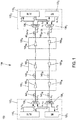
- FIG. 3 shows a block diagram of an optical repeater 150 j according to an embodiment. Connections of optical repeater 150 j to optical fibers 140 ja , 140 jb , 140 (j+1)a , and 140 (j+1)b of wet plant 104 are also shown in FIG. 3 to better indicate the relationship between the optical circuits of FIGs. 1 and 3 .
- Optical amplifier (OA) 160 ja of optical repeater 150 j (also see FIG. 1 ) is located in an optical path 340 a that connects optical fibers 140 ja and 140 (j+1)a .
- optical amplifier (OA) 160 jb of optical repeater 150 j also see FIG.
- Optical repeater 150 j also includes a supervisory optical circuit 300 that optically couples optical paths 340 a and 340 b as described in more detail below.
- Circuit 300 comprises (i) two 2 ⁇ 2 optical couplers that are labeled in FIG. 3 as 310 1b and 310 2a , respectively, and (ii) four 2 ⁇ 1 optical couplers that are labeled in FIG. 3 as 314, 318, 330 a , and 330 b , respectively.
- Optical coupler 310 2a is located on optical path 340 a at an output port 362 a of optical amplifier 160 ja .
- Optical coupler 310 1b is located on optical path 340 b at an output port 362 b of optical amplifier 160 jb .
- Optical coupler 330 a is located at input port 358 a of optical amplifier 160 ja .
- Optical coupler 330 b is located at input port 358 b of optical amplifier 160 jb .
- Optical coupler 310 1b and optical coupler 330 a are connected to one another by way of an optical fiber or waveguide 312.
- Optical coupler 310 2a and optical coupler 330 b are connected to one another by way of an optical fiber or waveguide 316.
- Optical coupler 314 is inserted into optical fiber or waveguide 312 to provide a parallel optical path between optical couplers 310 1b and 330 a , the parallel optical path comprising an NBPOF 320 1b .
- the transfer function 202 of NBPOF 320 1b has the center frequency f c corresponding to wavelength ⁇ 1 .
- Optical coupler 318 is similarly inserted into optical fiber or waveguide 316 to provide a parallel optical path between optical couplers 310 2a and 330 b , the parallel optical path comprising an NBPOF 320 2a .
- the transfer function 202 of NBPOF 320 2a has the center frequency f c corresponding to wavelength ⁇ 2 .
- circuit 300 can be a planar lightwave circuit or a part of a planar lightwave circuit.
- circuit 300 provides the following loop-back paths for the supervisory optical signals of carrier wavelengths ⁇ 1 and ⁇ 2 .
- a portion of a supervisory optical signal of carrier wavelength ⁇ 2 received from optical fiber 140 ja can be looped back into optical fiber 140 jb , e.g., as follows.
- Optical path 340 a directs the optical signal received through optical fiber 140 ja to optical amplifier 160 ja , where the latter undergoes optical amplification.
- the resulting amplified signal is directed from output port 362 a of optical amplifier 160 ja to optical coupler 310 2a .
- Optical coupler 310 2a operates to cause the coupled optical signal to be directed through NBPOF 320 2a that passes the ⁇ 2 component thereof and essentially stops all other spectral components thereof.
- the filtered ⁇ 2 component is coupled by optical coupler 318 into optical fiber 316, which directs it to optical amplifier 160 jb by way of optical coupler 330 b .
- the resulting amplified signal of carrier wavelength ⁇ 2 is then directed from output port 362 b of optical amplifier 160 jb to optical fiber 140 jb .
- a portion of a supervisory optical signal of carrier wavelength ⁇ 1 received from optical fiber 140 (j+1)b can be looped back into optical fiber 140 (j+1)a , e.g., as follows.
- Optical path 340 b directs the optical signal received through optical fiber 140 (j+1)b to optical amplifier 160 jb , where the latter undergoes optical amplification.
- the resulting amplified signal is directed from output port 362 b of optical amplifier 160 jb to optical coupler 310 1b .
- Optical coupler 310 1b operates to cause the coupled optical signal to be directed through NBPOF 320 1b that passes the ⁇ 1 component thereof and essentially stops all other spectral components thereof.
- the filtered ⁇ 1 component is coupled by optical coupler 314 into optical fiber 312, which directs it to optical amplifier 160 ja by way of optical coupler 330 a .
- the resulting amplified signal of carrier wavelength ⁇ 1 is then directed from output port 362 a of optical amplifier 160 ja to optical fiber 140 ( j+1)a .
- circuit 300 provides (i) an optical pathway for the backscattered light to cross from optical path 340 a to optical path 340 b and (ii) an optical pathway for the backscattered light to cross from optical path 340 b to optical path 340 a , both of these optical pathways being configured to bypass NBPOFs 320 1b and 320 2a .
- each of the latter optical pathways can be used to direct back to the corresponding one of landing stations 102 1 and 102 2 the backscattered light by way of the optical path having the optical amplifiers 160 that are directionally aligned with the propagation direction of the backscattered light.
- the backscattered light so directed can be of any suitable wavelength, e.g., have one of carrier wavelengths ⁇ 3 - ⁇ n or any out-of-band wavelength, such as a wavelength corresponding to a different telecom band than that of wavelengths ⁇ 1 - ⁇ n .
- optical fiber or waveguide 316 is configured to direct backscattered light received from optical fiber 140 (j+1)a to input port 358 b of optical amplifier 160 jb such that the received backscattered light bypasses NBPOF 320 2a .
- Optical fiber or waveguide 312 is similarly configured to direct backscattered light received from optical fiber 140 jb to input port 358 a of optical amplifier 160 ja such that the received backscattered light bypasses NBPOF 320 1b .
- the backscattered light can be generated by a number of physical mechanisms, such as (i) a catastrophic defect in the optical fiber; (ii) a relatively large temperature gradient along the length of the optical fiber; (iii) a non-catastrophic defect that might be caused by sheering, stressing, shaking, and/or excessive bending of the optical fiber; etc.
- Example optical-link monitoring (OLM) functions that can be implemented using the backscattered light channeled through optical fibers or waveguides 312 and 316 can be based on one or more of the following approaches.
- a landing station 102 can be designed and configured to perform OTDR measurements in a normal operating mode, e.g., by detecting and processing reflected and/or backscattered optical signals having carrier wavelengths ⁇ 3 - ⁇ n .
- a landing station 102 can be designed and configured to perform OTDR measurements in a special OLM operating mode, during which the corresponding transceiver generates and applies to wet plant 104 a modulated optical signal with a waveform that facilitates OTDR measurements, e.g., in terms of providing a higher signal-to-noise ratio (SNR) and/or a better spatial resolution for OTDR measurements than those technically achievable with payload-carrying optical signals. Transmission of payload data may be temporarily halted while landing station 102 is in the OLM operating mode and may be resumed when the corresponding transceiver is switched back to the normal operating mode.
- SNR signal-to-noise ratio
- the above-mentioned OLM functions can be based on different types of OTDR measurements.
- landing station 102 can be designed and configured to perform OTDR measurements by detecting and processing the elastically reflected light and/or backscattered light produced due to Rayleigh scattering in wet plant 104.
- landing station 102 can be designed and configured to perform OTDR measurements by detecting and processing the backscattered light produced due to Brillouin scattering in wet plant 104.
- landing station 102 can be designed and configured to perform OTDR measurements by detecting and processing the backscattered light produced due to Raman scattering in wet plant 104.
- FIG. 4 shows a block diagram of an optical repeater 150 j according to another embodiment. Connections of optical repeater 150 j to optical fibers 140 ja , 140 jb , 140 (j+1 ) a , and 140 (j+1)b of wet plant 104 are also shown in FIG. 4 to better indicate the relationship between the optical circuits of FIGs. 1 and 4 .
- optical repeater 150 j shown in FIG. 4 is generally similar to the embodiment of optical repeater 150 j shown in FIG. 3 , and the two embodiments use many of the same components, which are labeled in FIGs. 3 and 4 using the same labels. These components are already described above in reference to FIG. 3 , and their description is not repeated here. Instead, the description given below primarily focuses on the differences between the embodiments of FIGs. 3 and 4 .
- supervisory optical circuit 300 is replaced by a supervisory optical circuit 400.
- Circuit 400 differs from circuit 300 as follows:
- circuit 400 provides the following loop-back paths for the supervisory optical signals of carrier wavelengths ⁇ 1 and ⁇ 2.
- a portion of a supervisory optical signal of carrier wavelength ⁇ 1 received from optical fiber 140 ja can be looped back into optical fiber 140 jb , e.g., as follows.
- Optical path 340 a directs the optical signal received through optical fiber 140 ja to optical coupler 310 1a .
- Optical coupler 310 1a operates to cause the coupled optical signal to be directed through NBPOF 320 1a that passes the ⁇ 1 component thereof and essentially stops all other spectral components thereof.
- the filtered ⁇ 1 component is coupled by optical coupler 414 into optical fiber 312, which directs it to optical fiber 140 jb by way of optical coupler 310 1b .
- a portion of a supervisory optical signal of carrier wavelength ⁇ 2 received from optical fiber 140 ja can be looped back into optical fiber 140 jb , e.g., as follows.
- Optical path 340 a directs the optical signal received through optical fiber 140 ja to optical amplifier 160 ja , where the latter undergoes optical amplification.
- the resulting amplified signal is directed from output port 362 a of optical amplifier 160 ja to optical coupler 310 2a .
- Optical coupler 310 2a operates to cause the coupled optical signal to be directed through NBPOF 320 2a that passes the ⁇ 2 component thereof and essentially stops all other spectral components thereof.
- the filtered ⁇ 2 component is coupled by optical coupler 418 into optical fiber 316, which directs it to optical amplifier 160 jb by way of optical coupler 310 2b .
- the resulting amplified signal of carrier wavelength ⁇ 2 is then directed from output port 362 b of optical amplifier 160 jb to optical fiber 140 jb .
- a portion of a supervisory optical signal of carrier wavelength ⁇ 2 received from optical fiber 140 (j+1)b can be looped back into optical fiber 140( j+1 ) a , e.g., as follows.
- Optical path 340 b directs the optical signal received through optical fiber 140 (j+1)b to optical coupler 310 2b .
- Optical coupler 310 2b operates to cause the coupled optical signal to be directed through NBPOF 320 2b that passes the ⁇ 2 component thereof and essentially stops all other spectral components thereof.
- the filtered ⁇ 2 component is coupled by optical coupler 418 into optical fiber 316, which directs it to optical fiber 140 (j+1)a by way of optical coupler 310 2a .
- a portion of a supervisory optical signal of carrier wavelength ⁇ 1 received from optical fiber 140 (j+1)b can be looped back into optical fiber 140 (j+1 ) a , e.g., as follows.
- Optical path 340 b directs the optical signal received through optical fiber 140 (j+1)b to optical amplifier 160 jb , where the latter undergoes optical amplification.
- the resulting amplified signal is directed from output port 362 b of optical amplifier 160 jb to optical coupler 310 1b .
- Optical coupler 310 1b operates to cause the coupled optical signal to be directed through NBPOF 320 1b that passes the ⁇ 1 component thereof and essentially stops all other spectral components thereof.
- the filtered ⁇ 1 component is coupled by optical coupler 414 into optical fiber 312, which directs it to optical amplifier 160 ja by way of optical coupler 310 1a .
- the resulting amplified signal of carrier wavelength ⁇ 1 is then directed from output port 362 a of optical amplifier 160 ja to optical fiber 140 ( j+1)a .
- circuit 400 provides the same optical pathways for the backscattered light as circuit 300, by way of optical fibers or waveguides 312 and 316.
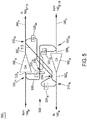
- FIG. 5 shows a block diagram of an optical repeater 150 j according to yet another embodiment. Connections of optical repeater 150 j to optical fibers 140 ja , 140 jb , 140 (j+1 ) a , and 140 (j+1)b of wet plant 104 are also shown in FIG. 5 to better indicate the relationship between the optical circuits of FIGs. I and 5 .
- supervisory optical circuit 400 is replaced by a supervisory optical circuit 500.
- Circuit 500 can be obtained by modifying circuit 400 as follows:
- circuit 500 provides the following loop-back paths for the supervisory optical signals of carrier wavelengths ⁇ 1 and ⁇ 2 .
- a portion of a supervisory optical signal of carrier wavelength ⁇ 1 received from optical fiber 140 ja can be looped back into optical fiber 140 jb , e.g., as follows.
- Optical path 340 a directs the optical signal received through optical fiber 140 ja to optical coupler 310 1a .
- Optical coupler 310 1a operates to cause the coupled optical signal to be directed through NBPOF 320 1a that passes the ⁇ 1 component thereof and essentially stops all other spectral components thereof.
- the filtered ⁇ 1 component is coupled by optical coupler 518 into optical fiber 516, which directs it to input port 358 b of optical amplifier 160 jb by way of optical coupler 310 2b .
- the resulting amplified signal of carrier wavelength ⁇ 1 is then directed from output port 362 b of optical amplifier 160 jb to optical fiber 140 jb .
- a portion of a supervisory optical signal of carrier wavelength ⁇ 2 received from optical fiber 140 ja can be looped back into optical fiber 140 jb , e.g., as follows.
- Optical path 340 a directs the optical signal received through optical fiber 140 ja to optical amplifier 160 ja , where the latter undergoes optical amplification.
- the resulting amplified signal is directed from output port 362 a of optical amplifier 160 ja to optical coupler 310 2a .
- Optical coupler 310 2a operates to cause the coupled optical signal to be directed through NBPOF 320 2a that passes the ⁇ 2 component thereof and essentially stops all other spectral components thereof.
- the filtered ⁇ 2 component is coupled by optical coupler 514 into optical fiber 512, which directs it to optical fiber 140 jb by way of optical coupler 310 1b .
- a portion of a supervisory optical signal of carrier wavelength ⁇ 2 received from optical fiber 140 (j+1)b can be looped back into optical fiber 140 (j+1)a , e.g., as follows.
- Optical path 340 b directs the optical signal received through optical fiber 140 (j+1)b to optical coupler 310 2b .
- Optical coupler 310 2b operates to cause the coupled optical signal to be directed through NBPOF 320 2b that passes the ⁇ 2 component thereof and essentially stops all other spectral components thereof.
- the filtered ⁇ 2 component is coupled by optical coupler 518 into optical fiber 516, which directs it to input port 358 a of optical amplifier 160 ja by way of optical coupler 310 1a .
- the resulting amplified signal of carrier wavelength ⁇ 2 is then directed from output port 362 a of optical amplifier 160 ja to optical fiber 140 (j+1 ) a .
- a portion of a supervisory optical signal of carrier wavelength ⁇ 1 received from optical fiber 140 (j+1)b can be looped back into optical fiber 140 (j+1)a , e.g., as follows.
- Optical path 340 b directs the optical signal received through optical fiber 140 (j+1)b to optical amplifier 160 jb , where the latter undergoes optical amplification.
- the resulting amplified signal is directed from output port 362 b of optical amplifier 160 jb to optical coupler 310 1b .
- Optical coupler 310 1b operates to cause the coupled optical signal to be directed through NBPOF 320 1b that passes the ⁇ 1 component thereof and essentially stops all other spectral components thereof.
- the filtered ⁇ 1 component is coupled by optical coupler 514 into optical fiber 512, which directs it to optical fiber 140 (j+1 ) a by way of optical coupler 310 2a .
- circuit 500 provides (i) an optical pathway, by way of optical fiber or waveguide 512 , for the backscattered light to cross from optical path 340 a to optical path 340 b and (ii) an optical pathway, by way of optical fiber or waveguide 512, for the backscattered light to cross from optical path 340 b to optical path 340 a , both of the latter optical pathways being configured to bypass NBPOFs 320 1a , 320 1b , 320 2a , and 320 2b .
- circuit 500 can be modified by removing the supervisory optical path between input ports 358 a and 358 b . In some other embodiments, circuit 500 can be modified by removing the supervisory optical path between output ports 362 a and 362 b .
- FIG. 6 shows a block diagram of an optical repeater 150 j according to yet another embodiment. Connections of optical repeater 150 j to optical fibers 140 ja , 140 jb , 140 (j +1 )a , and 140 (j+1)b of wet plant 104 are also shown in FIG. 6 to better indicate the relationship between the optical circuits of FIGs. 1 and 6 .
- supervisory optical circuit 300 ( FIG. 3 ) is replaced by a supervisory optical circuit 600.
- Circuit 600 can be obtained by adding to circuit 300 a supervisory optical path between input ports 358 a and 358 b .
- the added supervisory optical path comprises: (i) optical couplers 310 1a and 310 2b ; and (ii) optical fibers or waveguides 602 and 604, all connected as indicated in FIG. 6 .
- the added supervisory optical path is configured to use the wavelengths ⁇ 1 and ⁇ 2 to carry signals in respective opposite directions.
- circuit 600 provides the following loop-back paths for the supervisory optical signals of carrier wavelengths ⁇ 1 and ⁇ 2 .
- a portion of a supervisory optical signal of carrier wavelength ⁇ 1 received from optical fiber 140 ja can be looped back into optical fiber 140 jb , e.g., as follows.
- Optical path 340 a directs the optical signal received through optical fiber 140 ja to optical coupler 310 1a .
- Optical coupler 310 1a operates to cause the coupled optical signal to be directed through NBPOF 320 1a that passes the ⁇ 1 component thereof and essentially stops all other spectral components thereof.
- the filtered ⁇ 1 component is directed by optical fiber 602 to optical coupler 310 2b , which further directs it to input port 358 b of optical amplifier 160 jb .
- the resulting amplified signal of carrier wavelength ⁇ 1 is then directed from output port 362 b of optical amplifier 160 jb to optical fiber 140 jb .
- a portion of a supervisory optical signal of carrier wavelength ⁇ 2 received from optical fiber 140 ja can be looped back into optical fiber 140 jb , e.g., as follows.
- Optical path 340 a directs the optical signal received through optical fiber 140 ja to optical amplifier 160 ja , where the latter undergoes optical amplification.
- the resulting amplified signal is directed from output port 362 a of optical amplifier 160 ja to optical coupler 310 2a .
- Optical coupler 310 2a operates to cause the coupled optical signal to be directed through NBPOF 320 2a that passes the ⁇ 2 component thereof and essentially stops all other spectral components thereof.
- the filtered ⁇ 2 component is coupled by optical coupler 318 into optical fiber 316, which directs it to optical amplifier 160 jb by way of optical coupler 330 b .
- the resulting amplified signal of carrier wavelength ⁇ 2 is then directed from output port 362 b of optical amplifier 160 jb to optical fiber 140 jb .
- a portion of a supervisory optical signal of carrier wavelength ⁇ 1 received from optical fiber 140 (j+1)b can be looped back into optical fiber 140 (j+1)a , e.g., as follows.
- Optical path 340 b directs the optical signal received through optical fiber 140 (j+1)b to optical amplifier 160 jb , where the latter undergoes optical amplification.
- the resulting amplified signal is directed from output port 362 b of optical amplifier 160 jb to optical coupler 310 1b .
- Optical coupler 310 1b operates to cause the coupled optical signal to be directed through NBPOF 320 1b that passes the ⁇ 1 component thereof and essentially stops all other spectral components thereof.
- the filtered ⁇ 1 component is coupled by optical coupler 314 into optical fiber 312, which directs it to optical amplifier 160 ja by way of optical coupler 330 a .
- the resulting amplified signal of carrier wavelength ⁇ 1 is then directed from output port 362 a of optical amplifier 160 ja to optical fiber 140 (j+1)a .
- a portion of a supervisory optical signal of carrier wavelength ⁇ 2 received from optical fiber 140 (j+1)b can be looped back into optical fiber 140 (j+1 ) a , e.g., as follows.
- Optical path 340 b directs the optical signal received through optical fiber 140 (j+1)b to optical coupler 310 2b .
- Optical coupler 310 2b operates to cause the coupled optical signal to be directed through NBPOF 320 2b that passes the ⁇ 2 component thereof and essentially stops all other spectral components thereof.
- the filtered ⁇ 2 component is directed by optical fiber 604 to optical coupler 310 1a , which further directs it to input port 358 a of optical amplifier 160 ja .
- the resulting amplified signal of carrier wavelength ⁇ 2 is then directed from output port 362 a of optical amplifier 160 ja to optical fiber 140 ( j+1)a .
- circuit 600 provides the same optical pathways for the backscattered light as circuit 300, by way of optical fibers or waveguides 312 and 316.
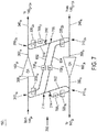
- FIG. 7 shows a block diagram of an optical repeater 150 j according to yet another embodiment. Connections of optical repeater 150 j to optical fibers 140 ja , 140 jb , 140 (j+1 ) a , and 140 (j+1)b of wet plant 104 are also shown in FIG. 7 to better indicate the relationship between the optical circuits of FIGs. 1 and 7 .
- supervisory optical circuit 600 ( FIG. 6 ) is replaced by a supervisory optical circuit 700.
- Circuit 700 differs from circuit 600 as follows:
- optical attenuators 706 1 -706 4 are also shown in FIG. 7 .
- Optical attenuator 706 1 is inserted between NBPOF 320 1b and optical coupler 314.
- Optical attenuator 706 2 is inserted between NBPOF 320 1b and optical coupler 314.
- Optical attenuator 706 3 is inserted into optical fiber 604 between optical coupler 310 1a and optical coupler 714.
- Optical attenuator 706 4 is inserted into optical fiber 602 between optical coupler 310 2b and optical coupler 718.
- Optical attenuators 706 1 -706 4 may be used in some embodiments to prevent spontaneous light generation in the "ring laser" that may be formed and become active due to the presence of output-to-input optical paths between optical amplifiers 160 ja and 160 ja provided by circuit 700.
- a person of ordinary skill in the art will understand that such spontaneous light generation may render optical repeater 150 j unusable, e.g., due to the high noise level caused thereby.
- the use of these and possibly other optional elements for the indicated purpose is not limited to the embodiment of optical repeater 150 j shown in FIG. 7 and, if necessary, may similarly be implemented in the embodiments of optical repeater 150 j shown in FIGs. 3-6 .
- circuit 700 provides the following loop-back paths for the supervisory optical signals of carrier wavelengths ⁇ 1 and ⁇ 2 .
- the description of these loop-back paths is given for an embodiment of circuit 700 in which optional optical attenuators 706 1 -706 4 are not present.
- a portion of a supervisory optical signal of carrier wavelength ⁇ 1 received from optical fiber 140 ja can be looped back into optical fiber 140 jb , e.g., as follows.
- Optical path 340 a directs the optical signal received through optical fiber 140 ja to optical coupler 310 1a .
- Optical coupler 310 1a operates to cause the coupled optical signal to be directed through NBPOF 320 1a that passes the ⁇ 1 component thereof and essentially stops all other spectral components thereof.
- the filtered ⁇ 1 component is directed by optical fiber 602, by way of optical coupler 718, to optical coupler 310 2b , which further directs it to input port 358 b of optical amplifier 160 jb .
- the resulting amplified signal of carrier wavelength ⁇ 1 is then directed from output port 362 b of optical amplifier 160 jb to optical fiber 140 jb .
- a portion of a supervisory optical signal of carrier wavelength ⁇ 2 received from optical fiber 140 ja can be looped back into optical fiber 140 jb , e.g., as follows.
- Optical path 340 a directs the optical signal received through optical fiber 140 ja to optical amplifier 160 ja , where the latter undergoes optical amplification.
- the resulting amplified signal is directed from output port 362 a of optical amplifier 160 ja to optical coupler 310 2a .
- Optical coupler 310 2a operates to cause the coupled optical signal to be directed through NBPOF 320 2a that passes the ⁇ 2 component thereof and essentially stops all other spectral components thereof.
- the filtered ⁇ 2 component is coupled by optical couplers 318 and 718 into optical fiber 602, which directs it to optical amplifier 160 jb by way of optical coupler 310 2b .
- the resulting amplified signal of carrier wavelength ⁇ 2 is then directed from output port 362 b of optical amplifier 160 jb to optical fiber 140 jb .
- a portion of a supervisory optical signal of carrier wavelength ⁇ 1 received from optical fiber 140 (j+1)b can be looped back into optical fiber 140 (j+1 ) a , e.g., as follows.
- Optical path 340 b directs the optical signal received through optical fiber 140 (j+1)b to optical amplifier 160 jb , where the latter undergoes optical amplification.
- the resulting amplified signal is directed from output port 362 b of optical amplifier 160 jb to optical coupler 310 1b .
- Optical coupler 310 1b operates to cause the coupled optical signal to be directed through NBPOF 320 1b that passes the ⁇ 1 component thereof and essentially stops all other spectral components thereof.
- the filtered ⁇ 1 component is coupled by optical couplers 314 and 714 into optical fiber 604, which directs it to optical amplifier 160 ja by way of optical coupler 310 1a .
- the resulting amplified signal of carrier wavelength ⁇ 1 is then directed from output port 362 a of optical amplifier 160 ja to optical fiber 140 (j+1)a .
- a portion of a supervisory optical signal of carrier wavelength ⁇ 2 received from optical fiber 140 (j+1)b can be looped back into optical fiber 140 (j+1 ) a , e.g., as follows.
- Optical path 340 b directs the optical signal received through optical fiber 140 (j+1)b to optical coupler 310 2b .
- Optical coupler 310 2b operates to cause the coupled optical signal to be directed through NBPOF 320 2b that passes the ⁇ 2 component thereof and essentially stops all other spectral components thereof.
- the filtered ⁇ 2 component is directed by optical fiber 604, by way of optical coupler 714, to optical coupler 310 1a , which further directs it to input port 358 a of optical amplifier 160 ja .
- the resulting amplified signal of carrier wavelength ⁇ 2 is then directed from output port 362 a of optical amplifier 160 ja to optical fiber 140 (j+1)a .
- circuit 700 provides substantially the same optical pathways for the backscattered light as circuit 600, by way of optical fibers or waveguides 312 and 316, which are merged with optical fibers or waveguides 604 and 602, respectively.
- an apparatus comprising: a first optical amplifier (e.g., 160 ja , FIG. 1 ) located in a first optical path (e.g., 340 a , FIGs. 3-7 ) and configured to amplify optical signals transmitted in a first direction; a second optical amplifier (e.g., 160 jb , FIG. 1 ) located in a second optical path (e.g., 340 b , FIGs. 3-7 ) and configured to amplify optical signals transmitted in a second direction, the second direction being opposite to the first direction; and an optical circuit (e.g., 300, FIG.
- an optical output port e.g., 362 a , FIG. 3
- a first optical port e.g., 358 b or 362 b , FIGs. 3, 5
- an optical connection, through the optical circuit, between the optical output port of the first optical amplifier and the first optical port of the second optical amplifier comprises: a first optical pathway (e.g., through 320 2a , FIG.
- the first optical pathway includes a first narrow band-pass optical filter (e.g., 320 2a , FIG. 3, 5 ) located therein; and wherein the second optical pathway is configured to bypass the first narrow band-pass optical filter.
- the first optical port is an input port (e.g., 358 b , FIG. 3 ) of the second optical amplifier.
- the first optical port is an output port (e.g., 362 b , FIG. 5 ) of the second optical amplifier.
- the optical connection, through the optical circuit, between the optical output port of the first optical amplifier and the first optical port of the second optical amplifier further comprises a third optical pathway (e.g., through 320 2b , FIG. 4 ; or through 320 1b , FIG. 5 ) configured to direct light traveling in the second direction at the first optical port of the second optical amplifier to the optical output port of the first optical amplifier in a manner that causes the light so directed to travel in the first direction at the optical output port of the first optical amplifier; and wherein the third optical pathway includes a second narrow band-pass optical filter (e.g., 320 2b , FIG. 4 ; or 320 1b , FIG. 5 ) located therein.
- a third optical pathway e.g., through 320 2b , FIG. 4 ; or through 320 1b , FIG. 5
- the second optical pathway is configured to bypass the second narrow band-pass optical filter.
- the first optical port is an input port (e.g., 358 b , FIG. 4 ) of the second optical amplifier.
- the first optical port is an output port (e.g., 362 b , FIG. 5 ) of the second optical amplifier.
- the first narrow band-pass optical filter has a transfer function (e.g., 202, FIG. 2 ) that causes the first narrow band-pass optical filter to pass a first wavelength (e.g., ⁇ 2 , FIG. 5 ) and reject a second wavelength (e.g., ⁇ 1 , FIG. 5 ); and wherein the second narrow band-pass optical filter has a transfer function (e.g., 202, FIG. 2 ) that causes the second narrow band-pass optical filter to pass the second wavelength and reject the first wavelength.
- a transfer function e.g., 202, FIG. 2
- each of the first and second optical amplifiers is configured to amplify a respective WDM signal transmitted therethrough, the respective WDM signal configured to include a plurality of spectral components, each of the spectral components having a respective wavelength (e.g., ⁇ 3 - ⁇ n , FIG. 1 ) different from the first and second wavelengths; and wherein the first wavelength, the second wavelength, and the respective wavelengths are spectrally arranged in accordance with a wavelength grid.
- the second narrow band-pass optical filter (e.g., 320 2b , FIG. 4 ) is a nominal copy of the first narrow band-pass optical filter (e.g., 320 2 a , FIG. 4 ).
- the optical circuit is further connected to optically couple an optical input port (e.g., 358 a , FIG. 3 ) of the first optical amplifier and a second optical port (e.g., 362 b or 358 b , FIGs. 3, 5 ) of the second optical amplifier; and wherein an optical connection, through the optical circuit, between the optical input port of the first optical amplifier and the second optical port of the second optical amplifier comprises: a third optical pathway (e.g., through 320 1b , FIG.
- a fourth optical pathway (e.g., 312, FIG. 3 ; 516, FIG. 5 ) configured to direct light traveling in the first direction at the second optical port of the second optical amplifier to the optical input port of the first optical amplifier in a manner that causes the light so directed to travel in the first direction at the optical input port of the first optical amplifier;
- the third optical pathway includes a second narrow band-pass optical filter (e.g., 320 1b , FIG. 3 ) located therein; and wherein the fourth optical pathway is configured to bypass the second narrow band-pass optical filter.
- the first optical port is an input port (e.g., 358 b , FIG. 3 ) of the second optical amplifier; and wherein the second optical port is an output port (e.g., 362 b , FIG. 3 ) of the second optical amplifier.
- the first optical port is an output port (e.g., 362 b , FIG. 5 ) of the second optical amplifier; and wherein the second optical port is an input port (e.g., 358 b , FIG. 5 ) of the second optical amplifier.
- the first narrow band-pass optical filter has a transfer function (e.g., 202, FIG. 2 ) that causes the first narrow band-pass optical filter to pass a first wavelength (e.g., ⁇ 2 , FIG. 3 ) and reject a second wavelength (e.g., ⁇ 1 , FIG. 3 ); and wherein the second narrow band-pass optical filter has a transfer function (e.g., 202, FIG. 2 ) that causes the second narrow band-pass optical filter to pass the second wavelength and reject the first wavelength.
- a transfer function e.g., 202, FIG. 2
- the optical connection, through the optical circuit, between the optical output port of the first optical amplifier and the first optical port of the second optical amplifier further comprises a fifth optical pathway (e.g., through 320 2b , FIG. 4 ) configured to direct light traveling in the second direction at the first optical port of the second optical amplifier to the optical output port of the first optical amplifier in a manner that causes the light so directed to travel in the first direction at the optical output port of the first optical amplifier; and wherein the fifth optical pathway includes a third narrow band-pass optical filter (e.g., 320 2b , FIG. 4 ) located therein.
- a third narrow band-pass optical filter e.g., 320 2b , FIG. 4
- the first narrow band-pass optical filter has a transfer function (e.g., 202, FIG. 2 ) that causes the first narrow band-pass optical filter to pass a first wavelength (e.g., ⁇ 2 , FIG. 3 ) and reject a second wavelength (e.g., ⁇ 1 , FIG. 3 ); wherein the second narrow band-pass optical filter has a transfer function (e.g., 202, FIG. 2 ) that causes the second narrow band-pass optical filter to pass the second wavelength and reject the first wavelength; and wherein the third narrow band-pass optical filter (e.g., 320 2b , FIG. 4 ) is a nominal copy of the first narrow band-pass optical filter (e.g., 320 2a , FIG. 4 ).
- a transfer function e.g., 202, FIG. 2
- the second narrow band-pass optical filter has a transfer function (e.g., 202, FIG. 2 ) that causes the second narrow band-pass optical filter to pass the second wavelength and reject
- the optical connection, through the optical circuit, between the optical input port of the first optical amplifier and the second optical port of the second optical amplifier further comprises a sixth optical pathway (e.g., through 320 1a , FIG. 4 ) configured to direct light traveling in the first direction at the optical in port of the first optical amplifier to the second optical port of the second optical amplifier in a manner that causes the light so directed to travel in the second direction at the second optical port of the second optical amplifier; and wherein the sixth optical pathway includes a fourth narrow band-pass optical filter (e.g., 320 1a , FIG. 4 ) located therein.
- a sixth optical pathway e.g., through 320 1a , FIG. 4
- the first narrow band-pass optical filter has a transfer function (e.g., 202, FIG. 2 ) that causes the first narrow band-pass optical filter to pass a first wavelength (e.g., ⁇ 2 , FIG. 3 ) and reject a second wavelength (e.g., ⁇ 1 , FIG. 3 ); wherein the second narrow band-pass optical filter has a transfer function (e.g., 202, FIG. 2 ) that causes the second narrow band-pass optical filter to pass the second wavelength and reject the first wavelength; wherein the third narrow band-pass optical filter (e.g., 320 2b , FIG.
- a transfer function e.g., 202, FIG. 2
- the fourth narrow band-pass optical filter e.g., 320 1a , FIG. 4
- the second narrow band-pass optical filter e.g., 320 1b , FIG. 4
- the first narrow band-pass optical filter has a transfer function (e.g., 202, FIG. 2 ) characterized by a bandwidth (e.g., B, FIG. 2A ); and wherein the first narrow band-pass optical filter does not employ a mirror configured to reflect in an opposite direction light applied thereto by the first optical pathway, the light being spectrally located within the bandwidth.
- the apparatus comprises a planar lightwave circuit (e.g., 300, FIG. 3 ), wherein the first narrow band-pass optical filter is a part of the planar lightwave circuit.
- Couple refers to any manner known in the art or later developed in which energy is allowed to be transferred between two or more elements, and the interposition of one or more additional elements is contemplated, although not required. Conversely, the terms “directly coupled,” “directly connected,” etc., imply the absence of such additional elements.
Landscapes
- Physics & Mathematics (AREA)
- Electromagnetism (AREA)
- Engineering & Computer Science (AREA)
- Computer Networks & Wireless Communication (AREA)
- Signal Processing (AREA)
- Optical Communication System (AREA)
Abstract
Description
- The present disclosure relates to optical communication equipment and, more specifically but not exclusively, to the use of band-pass filters in supervisory signal paths of an optical transport system.
- This section introduces aspects that may help facilitate a better understanding of the disclosure. Accordingly, the statements of this section are to be read in this light and are not to be understood as admissions about what is in the prior art or what is not in the prior art.
- Subsea network operators are facing a fast growth in bandwidth demand, in part due to the development and deployment of cloud-based services. As a result, they need to optimize the capacity and performance of their fiber-optic cable plants to enable the corresponding networks to efficiently handle the increasing data flows. Due to this need, one of the requirements to telecom equipment manufacturers is to provide the network operator(s) with a supervisory system that can be used to monitor the status of the submerged plant elements, e.g., to guarantee fault detection and diagnostics, improved maintainability, good performance characteristics throughout the plant's lifespan, upgradable capacity, and/or any other pertinent benchmarks. It is also desirable for the supervisory system to be amenable to a low-cost implementation.
- At least some of the above-indicated problems in the state of the art are addressed by various embodiments of a bidirectional optical repeater having two unidirectional optical amplifiers and a supervisory optical circuit connected to optically couple the optical ports thereof. In an example embodiment, the supervisory optical circuit provides one or more pathways therethrough for supervisory optical signals, each of these pathways having located therein a respective narrow band-pass optical filter. The supervisory optical circuit further provides one or more pathways therethrough configured to bypass the corresponding narrow band-pass optical filters in a manner that enables backscattered light of any wavelength to cross into the optical path that has therein the unidirectional optical amplifier directionally aligned with the propagation direction of the backscattered light.
- According to an example embodiment, provided is an apparatus comprising: a first optical amplifier located in a first optical path and configured to amplify optical signals transmitted in a first direction; a second optical amplifier located in a second optical path and configured to amplify optical signals transmitted in a second direction, the second direction being opposite to the first direction; and an optical circuit connected to optically couple an optical output port of the first optical amplifier and a first optical port of the second optical amplifier; and wherein an optical connection, through the optical circuit, between the optical output port of the first optical amplifier and the first optical port of the second optical amplifier comprises: a first optical pathway configured to direct light traveling in the first direction at the optical output port of the first optical amplifier to the first optical port of the second optical amplifier in a manner that causes the light so directed to travel in the second direction at the first optical port of the second optical amplifier; and a second optical pathway configured to direct light traveling in the second direction at the optical output port of the first optical amplifier to the first optical port of the second optical amplifier in a manner that causes the light so directed to travel in the second direction at the first optical port of the second optical amplifier; wherein the first optical pathway includes a first narrow band-pass optical filter located therein; and wherein the second optical pathway is configured to bypass the first narrow band-pass optical filter.
- Other aspects, features, and benefits of various disclosed embodiments will become more fully apparent, by way of example, from the following detailed description and the accompanying drawings, in which:
-
FIG. 1 shows a block diagram of an optical transport system according to an embodiment; -
FIGs. 2A-2B graphically illustrate certain spectral characteristics of an example narrow band-pass optical filter that can be used in a supervisory optical circuit of an optical repeater of the optical transport system ofFIG. 1 according to an embodiment; -
FIG. 3 shows a block diagram of an optical repeater that can be used in the optical transport system ofFIG. 1 according to an embodiment; -
FIG. 4 shows a block diagram of an optical repeater that can be used in the optical transport system ofFIG. 1 according to another embodiment; -
FIG. 5 shows a block diagram of an optical repeater that can be used in the optical transport system ofFIG. 1 according to yet another embodiment; -
FIG. 6 shows a block diagram of an optical repeater that can be used in the optical transport system ofFIG. 1 according to yet another embodiment; and -
FIG. 7 shows a block diagram of an optical repeater that can be used in the optical transport system ofFIG. 1 according to yet another embodiment. - Some embodiments may benefit from the use of features disclosed in the concurrently filed patent application by Omar Ait Sab and Ludivine Moirot, entitled "SUPERVISORY SIGNAL PATHS FOR AN OPTICAL TRANSPORT SYSTEM," attorney reference number 820470, which is incorporated herein by reference in its entirety.
-
FIG. 1 shows a block diagram of anoptical transport system 100 according to an embodiment. In the shown embodiment,system 100 comprises landing stations 102 1 and 102 2 connected by way of awet plant 104. Landing stations 102 1 and 102 2 are typically further connected to respective terrestrial networks (not explicitly shown inFIG. 1 ). In an alternative embodiment,system 100 may have additional landing stations connected towet plant 104, as known in the pertinent art, e.g., using one or more branching units (not explicitly shown inFIG. 1 ). - In an example embodiment,
wet plant 104 comprises an undersea cable system that includes, inter alia, submersible optical repeaters 1501 -150N serially connected byspans 140 of optical fiber, e.g., as indicated inFIG. 1 , where N is a positive integer. In the shown embodiment, eachspan 140i includes two optical fibers, which are labeled 140ia and 140ib , respectively, where i=l, 2, ..., N+1. The number N ofoptical repeaters 150 used inwet plant 104 depends on the particular embodiment and may be in the range, e.g., from 1 to ∼200. A typical length of afiber span 140i may range from ∼75 km to ∼100 km, depending on the distance between landing stations 1021 and 1022 . - In the shown embodiment, an
optical repeater 150j comprisesoptical amplifiers Optical amplifier 160ja is configured to amplify optical signals traveling towards landing station 1022 .Optical amplifier 160jb is similarly configured to amplify optical signals traveling towards landing station 1021 . In an example embodiment, anoptical amplifier 160j can be implemented as known in the pertinent art, e.g., using an erbium-doped fiber, a gain-flattening filter, and one or more laser-diode pumps. The laser diodes can be powered by a DC current from the corresponding shore-based power-feeding equipment (PFE, not explicitly shown inFIG. 1 ), fed through the center conductor(s) of the corresponding submarine cable, which also typically containsoptical fibers - In an alternative embodiment,
optical repeaters 150 can be designed for two, three, four, or more pairs ofoptical fibers 140i connected thereto at each side thereof. For example, anoptical repeater 150 designed to be compatible with a four-fiber-pair submarine cable typically includes eightoptical amplifiers 160 arranged in four amplifier pairs, each pair being similar tooptical amplifiers -
Optical repeater 150j further comprises a supervisory optical circuit (not explicitly shown inFIG. 1 ) that enables monitoring equipment (ME) units 1201 and 1202 located at landing stations 1021 and 1022 , respectively, to monitor the operating status of the optical repeaters, e.g., as further described below. Example embodiments of the supervisory optical circuit that can be used inoptical repeater 150j are described in more detail below in reference toFIGs. 2-7 . - In an example embodiment, each of ME units 1201 and 1202 is configured to use dedicated supervisory wavelengths (labeled λ1 and λ2) to generate respective supervisory signals that can be sent through the corresponding fiber(s) 140 towards the remote landing station 102. The supervisory optical circuit of each
optical repeater 150j is configured to loop back, in the opposite direction, at least a portion of a supervisory signal. As a result, ME unit 1201 can receive a looped-back supervisory signal comprising the portions of the original supervisory signal returned to that ME unit by the different supervisory optical circuits of different optical repeaters 1501-150N. Similarly, ME unit 1202 can receive a looped-back supervisory signal comprising the portions of the corresponding supervisory signal returned to that ME unit by the different supervisory optical circuits of different optical repeaters 1501-150N. The looped-back supervisory signals received by ME units 1201 and 1202 can be processed and analyzed to determine the present operating status and/or certain operating characteristics of at least some or all of optical repeaters 1501-150N inwet plant 104. The determined parameters may include but are not limited to: (i) input and output signal levels and the gains of some or all individualoptical amplifiers optical fibers 140i , such as any gradual loss increases therein; and (iii) catastrophic failures in individualoptical repeaters 150j and/oroptical fibers 140i . - Landing station 1021 comprises a submarine line terminal equipment (SLTE) unit 1101 and ME unit 1201 connected to
wet plant 104 by way of a wavelength multiplexer (MUX) 1301 and a wavelength de-multiplexer (DMUX) 1361 as indicated inFIG. 1 . In an example embodiment, SLTE unit 1101 includes a wavelength-division-multiplexing (WDM) transceiver (not explicitly shown inFIG. 1 ) configured to transmit and receive payload-carrying optical signals using carrier wavelengths λ3-λn, where n generally denotes the number of WDM channels insystem 100. The number n can be in the range between ∼10 and ∼150. - As already indicated above, carrier wavelengths λ1 and λ2 are reserved for supervisory signals and are not used by SLTE unit 1101 for payload transmissions. Carrier wavelengths λ1 and λ2 can be spectrally located at an edge of the spectral range occupied by the payload-carrying WDM channels. For example, in some embodiments, both carrier wavelengths λ1 and λ2 can be smaller than any of carrier wavelengths λ3-λn. In some other embodiments, both carrier wavelengths λ1 and λ2 can be larger than any of carrier wavelengths λ3-λn. In some alternative embodiments, carrier wavelength λ1 can be smaller than any of carrier wavelengths λ3-λn, and carrier wavelength λ2 can be larger than any of carrier wavelengths λ3-λn.
- In an example embodiment, carrier wavelengths λ1-λn can be selected in accordance with a frequency (wavelength) grid, such as a frequency grid that complies with the ITU-T G.694.1 Recommendation, which is incorporated herein by reference in its entirety. The frequency grid used in
system 100 can be defined, e.g., in the frequency range from about 184 THz to about 201 THz, with a 100, 50, 25, or 12.5-GHz spacing of the channels therein. While typically defined in frequency units, the parameters of the grid can equivalently be expressed in wavelength units. For example, in the wavelength range from about 1528 nm to about 1568 nm, the 100-GHz spacing between the centers of neighboring WDM channels is equivalent to approximately 0.8-nm spacing. In alternative embodiments, other fixed or flexible (flex) frequency grids can be used as well. - In operation, MUX 1301 multiplexes the optical signals of carrier wavelengths λ3-λn generated by SLTE unit 1101 and the supervisory optical signals of carrier wavelengths λ1 and λ2, and applies the resulting multiplexed optical signal to
optical fiber 1401a . DMUX 1361 demultiplexes a multiplexed optical signal received fromoptical fiber 1401b into two portions. The first portion has optical signals of carrier wavelengths λ3-λn and is directed to SLTE unit 1101 . The second portion has the looped-back supervisory optical signals of carrier wavelengths λ1 and λ2 and is directed to ME unit 1201 . - In an example embodiment, ME unit 1201 comprises an optical time-domain reflectometer (OTDR, not explicitly shown in
FIG. 1 ) configured to optically probewet plant 104 using carrier wavelengths λ1 and λ2. For example, ME unit 1201 can be designed to perform OTDR measurements by detecting and processing the looped-back supervisory optical signals received from optical repeaters 1501-150N . In general, ME unit 1201 can be configured to use any suitable OTDR method. Some embodiments of ME unit 1201 may benefit from the use of at least some OTDR features and/or techniques disclosed, e.g., inU.S. Patent Nos. 9,341,543 9,310,274 9,240,836 9,170,173 9,143,228 9,042,721 9,036,991 9,008,503 8,942,556 ,8,837,938 ,8,805,183 ,8,502,964 , and8,280,253 andU.S. Patent Application Publication Nos. 2011/0216996 ,2013/0216176 , and2014/0212130 , all of which are incorporated herein by reference in their entirety. The general physical principles of different types of OTDR measurements are reviewed, e.g., in Xiaoyi Bao and Liang Chen, "Recent Progress in Distributed Fiber Optic Sensors," Sensors, 2012, vol. 12, pp. 8601-8639, which is also incorporated herein by reference in its entirety. - Landing station 102 2 is analogous to landing station 1021 and comprises an SLTE unit 1102 , ME unit 1202 , a
MUX 1302 , and a DMUX 1362 . The analogous elements/components of the two landing stations are labeled inFIG. 1 using the same numerical labels, but with different respective subscripts. The descriptions of SLTE unit 1101 , ME unit 1201 ,MUX 1301 , and DMUX 1361 of landing station 1021 given above generally apply to SLTE unit 1102 , ME unit 1202 ,MUX 1302 , and DMUX 1362 , respectively, of landing station 102 2 and are not repeated here. - In various embodiments, each of landing stations 1021 and 102 2 may further include one or more of the following conventional elements/components: (i) power feeding equipment; (ii) system supervisory equipment; (iii) network management equipment; (iv) cable termination boxes; (v) network protection equipment; and (vi) various interface circuits.
- In some embodiments, a single respective carrier wavelength can be used at each of ME units 1201 and 1202 to generate supervisory optical signals. In some other embodiments, more than two carrier wavelengths of the WDM set λ1-λn can be allocated for supervisory functions. A person of ordinary skill in the art will understand, without undue experimentation, how to modify
MUXes 130, DMUXes 136, and/or other pertinent system components to be compatible with such alternative WDM-channel allocations for supervisory functions. - In an example embodiment, a supervisory optical circuit of
optical repeater 150j is implemented using narrow band-pass optical filters (NBPOFs, not explicitly shown inFIG. 1 , seeFIGs. 2-7 ). - As used herein the term "narrow band-pass optical filter" refers to an optical device that passes optical frequencies (wavelengths) within a certain relatively narrow range and rejects (or strongly attenuates) optical frequencies outside that range. The bandwidth B of the narrow band-pass optical filter is much smaller than any of the carrier frequencies that are being passed therethrough. For example, a center frequency of the pass band can be ∼200 THz, whereas the bandwidth B can be ∼100 GHz, which is approximately three orders of magnitude smaller.
- The planar-lightwave-circuit (PLC) technology enables telecom equipment manufacturers to produce narrow band-pass optical filters in large quantities and/or relatively inexpensively. There are many mature filter designs from which the manufacturer can choose for the intended application. In addition, a PLC-based narrow band-pass optical filter can be made tunable in a relatively straightforward manner, without an expensive and/or time-consuming redesign.
- Various embodiments disclosed herein can beneficially leverage some of these and other technical features of narrow band-pass optical filters to provide a supervisory optical circuit for
optical repeater 150j that is capable of meeting and/or exceeding the operating requirements of network operator(s) and is amenable to low-cost implementation. In addition, at least some of the disclosed embodiments can beneficially provide significant flexibility in the manner in which supervisory optical circuits can be designed and/or operated. -
FIGs. 2A-2B graphically illustrate certain spectral characteristics of an example narrow band-pass optical filter that can be used in the supervisory optical circuit ofoptical repeater 150j according to an embodiment. More specifically,FIG. 2A graphically shows amagnitude transfer function 202 versus frequency for a narrow band-pass optical filter.FIG. 2B graphically shows the spectral alignment oftransfer function 202 with aspectrum 210 of an example WDM signal that can be used insystem 100. - Referring to
FIG. 2A , marked on the abscissa are (i) the center frequency fc oftransfer function 202 and (ii) the frequencies fl and fh of the half-power points (gain -3 dB relative to the center portion) oftransfer function 202. The bandwidth B oftransfer function 202 can typically be defined as the difference between the frequencies fh and fl, although an alternative definition is also possible. - Depending on the embodiment, the bandwidth B can be, e.g., 100, 50, 25, or 12.5 GHz. Other values of the bandwidth B can also be used, as long as the selected bandwidth value is compatible with the system's WDM configuration and/or WDM-channel assignment, e.g., as further illustrated in
FIG. 2B . - The center frequency fc can belong to any telecom band. As known to those skilled in the pertinent art, the frequencies (wavelengths) used for optical communications are conventionally divided into several spectral bands in which optical fibers have relatively low transmission losses. For example, the spectral range between 1260 nm and 1625 nm is divided into five telecom bands that are typically referred to as O-, E-, S-, C-, and L-bands. The O-band is in the wavelength range between 1260 nm and 1360 nm. The E-band is in the wavelength range between 1360 nm and 1460 nm. The S-band is in the wavelength range between 1460 nm and 1530 nm. The C-band is in the wavelength range between 1530 nm and 1565 nm. The L-band is in the wavelength range between 1565 nm and 1625 nm.
- Referring to
FIG. 2B ,spectrum 210 has fifty-one peaks corresponding to carrier wavelengths λ1-λ51 (i.e., n-51).Transfer function 202 is illustratively shown as being spectrally aligned with the peak corresponding to carrier wavelength λ1, which is one of the dedicated supervisory wavelengths in system 100 (seeFIG. 1 ). The center frequency fc and bandwidth B oftransfer function 202 are such that a supervisory optical signal having carrier wavelength can pass through the corresponding narrow band-pass optical filter with little attenuation, whereas any of the optical signals having carrier wavelengths λ2-λ51 is rejected or significantly attenuated due to being outside of the bandwidth B. - A person of ordinary skill in the art will understand that a narrow band-pass optical filter corresponding to any of the additional dedicated supervisory wavelengths (e.g., λ2,
FIG. 1 ) can similarly be spectrally aligned with the peak corresponding to that carrier wavelength inspectrum 210. - In an example embodiment, any of the narrow band-pass optical filters used in supervisory optical circuits disclosed herein can be implemented as a part of the corresponding planar lightwave circuit. In a typical design, such a narrow band-pass optical filter does not employ a mirror configured to reflect, in an opposite direction, light applied to the filter by the corresponding supervisory optical circuit, e.g., if the light has a carrier frequency between fh and f1 (see
FIG. 2A ). As used herein, the term "mirror" should be construed to cover, inter alia, conventional broadband mirrors, wavelength-selective reflectors, and Bragg reflectors. -
FIG. 3 shows a block diagram of anoptical repeater 150j according to an embodiment. Connections ofoptical repeater 150j tooptical fibers wet plant 104 are also shown inFIG. 3 to better indicate the relationship between the optical circuits ofFIGs. 1 and3 . Optical amplifier (OA) 160ja of optical repeater 150j (also seeFIG. 1 ) is located in anoptical path 340a that connectsoptical fibers FIG. 1 ) is located in anoptical path 340b that connectsoptical fibers Optical repeater 150j also includes a supervisoryoptical circuit 300 that optically couplesoptical paths -
Circuit 300 comprises (i) two 2×2 optical couplers that are labeled inFIG. 3 as 3101b and 3102a , respectively, and (ii) four 2×1 optical couplers that are labeled inFIG. 3 as 314, 318, 330a , and 330b , respectively. Optical coupler 3102a is located onoptical path 340a at anoutput port 362a ofoptical amplifier 160ja . Optical coupler 3101b is located onoptical path 340b at anoutput port 362b ofoptical amplifier 160jb .Optical coupler 330a is located atinput port 358a ofoptical amplifier 160ja .Optical coupler 330b is located atinput port 358b ofoptical amplifier 160jb . Optical coupler 3101b andoptical coupler 330a are connected to one another by way of an optical fiber orwaveguide 312. Optical coupler 3102a andoptical coupler 330b are connected to one another by way of an optical fiber orwaveguide 316. -
Optical coupler 314 is inserted into optical fiber orwaveguide 312 to provide a parallel optical path betweenoptical couplers 3101b and 330a , the parallel optical path comprising anNBPOF 3201b . Thetransfer function 202 ofNBPOF 3201b has the center frequency fc corresponding to wavelength λ1. -
Optical coupler 318 is similarly inserted into optical fiber orwaveguide 316 to provide a parallel optical path betweenoptical couplers 3102a and 330b , the parallel optical path comprising anNBPOF 3202a . Thetransfer function 202 ofNBPOF 3202a has the center frequency fc corresponding to wavelength λ2. - In an example embodiment,
circuit 300 can be a planar lightwave circuit or a part of a planar lightwave circuit. - In operation,
circuit 300 provides the following loop-back paths for the supervisory optical signals of carrier wavelengths λ1 and λ2. - A portion of a supervisory optical signal of carrier wavelength λ2 received from
optical fiber 140ja can be looped back intooptical fiber 140jb , e.g., as follows.Optical path 340a directs the optical signal received throughoptical fiber 140ja tooptical amplifier 160ja , where the latter undergoes optical amplification. The resulting amplified signal is directed fromoutput port 362a ofoptical amplifier 160ja to optical coupler 3102a . Optical coupler 3102a operates to cause the coupled optical signal to be directed throughNBPOF 3202a that passes the λ2 component thereof and essentially stops all other spectral components thereof. The filtered λ2 component is coupled byoptical coupler 318 intooptical fiber 316, which directs it tooptical amplifier 160jb by way ofoptical coupler 330b . The resulting amplified signal of carrier wavelength λ2 is then directed fromoutput port 362b ofoptical amplifier 160jb tooptical fiber 140jb . - A portion of a supervisory optical signal of carrier wavelength λ1 received from
optical fiber 140(j+1)b can be looped back intooptical fiber 140(j+1)a , e.g., as follows.Optical path 340b directs the optical signal received throughoptical fiber 140(j+1)b tooptical amplifier 160jb , where the latter undergoes optical amplification. The resulting amplified signal is directed fromoutput port 362b ofoptical amplifier 160jb to optical coupler 3101b . Optical coupler 3101b operates to cause the coupled optical signal to be directed throughNBPOF 3201b that passes the λ1 component thereof and essentially stops all other spectral components thereof. The filtered λ1 component is coupled byoptical coupler 314 intooptical fiber 312, which directs it tooptical amplifier 160ja by way ofoptical coupler 330a . The resulting amplified signal of carrier wavelength λ1 is then directed fromoutput port 362a ofoptical amplifier 160ja tooptical fiber 140 (j+1)a . - In addition,
circuit 300 provides (i) an optical pathway for the backscattered light to cross fromoptical path 340a tooptical path 340b and (ii) an optical pathway for the backscattered light to cross fromoptical path 340b tooptical path 340a , both of these optical pathways being configured to bypassNBPOFs optical amplifiers 160 that are directionally aligned with the propagation direction of the backscattered light. The backscattered light so directed can be of any suitable wavelength, e.g., have one of carrier wavelengths λ3-λn or any out-of-band wavelength, such as a wavelength corresponding to a different telecom band than that of wavelengths λ1-λn. - For example, optical fiber or
waveguide 316 is configured to direct backscattered light received fromoptical fiber 140(j+1)a to inputport 358b ofoptical amplifier 160jb such that the received backscattered light bypassesNBPOF 3202a . Optical fiber orwaveguide 312 is similarly configured to direct backscattered light received fromoptical fiber 140jb to inputport 358a ofoptical amplifier 160ja such that the received backscattered light bypassesNBPOF 3201b . A person of ordinary skill in the art will understand that the capability for efficiently channeling the backscattered light towards the source of the original optical signal that is being backscattered can advantageously be used, e.g., to expand the monitoring capabilities of landing stations 1021 and 102 2 beyond the above-described capabilities of ME units 120. - As known in the pertinent art, the backscattered light can be generated by a number of physical mechanisms, such as (i) a catastrophic defect in the optical fiber; (ii) a relatively large temperature gradient along the length of the optical fiber; (iii) a non-catastrophic defect that might be caused by sheering, stressing, shaking, and/or excessive bending of the optical fiber; etc.
- Example optical-link monitoring (OLM) functions that can be implemented using the backscattered light channeled through optical fibers or
waveguides - In some embodiments, a landing station 102 can be designed and configured to perform OTDR measurements in a normal operating mode, e.g., by detecting and processing reflected and/or backscattered optical signals having carrier wavelengths λ3-λn. Alternatively or in addition, a landing station 102 can be designed and configured to perform OTDR measurements in a special OLM operating mode, during which the corresponding transceiver generates and applies to wet plant 104 a modulated optical signal with a waveform that facilitates OTDR measurements, e.g., in terms of providing a higher signal-to-noise ratio (SNR) and/or a better spatial resolution for OTDR measurements than those technically achievable with payload-carrying optical signals. Transmission of payload data may be temporarily halted while landing station 102 is in the OLM operating mode and may be resumed when the corresponding transceiver is switched back to the normal operating mode.
- In different embodiments, the above-mentioned OLM functions can be based on different types of OTDR measurements. For example, in one possible embodiment, landing station 102 can be designed and configured to perform OTDR measurements by detecting and processing the elastically reflected light and/or backscattered light produced due to Rayleigh scattering in
wet plant 104. In another possible embodiment, landing station 102 can be designed and configured to perform OTDR measurements by detecting and processing the backscattered light produced due to Brillouin scattering inwet plant 104. In yet another possible embodiment, landing station 102 can be designed and configured to perform OTDR measurements by detecting and processing the backscattered light produced due to Raman scattering inwet plant 104. These and other embodiments may benefit from the use of at least some OTDR features and/or techniques disclosed in the above-citedU.S. Patent Nos. 9,341,543 9,310,274 9,240,836 9,170,173 9,143,228 9,042,721 9,036,991 9,008,503 8,942,556 ,8,837,938 ,8,805,183 ,8,502,964 , and8,280,253 andU.S. Patent Application Publication Nos. 2011/0216996 ,2013/0216176 , and2014/0212130 . -
FIG. 4 shows a block diagram of anoptical repeater 150j according to another embodiment. Connections ofoptical repeater 150j tooptical fibers wet plant 104 are also shown inFIG. 4 to better indicate the relationship between the optical circuits ofFIGs. 1 and4 . - The embodiment of
optical repeater 150j shown inFIG. 4 is generally similar to the embodiment ofoptical repeater 150j shown inFIG. 3 , and the two embodiments use many of the same components, which are labeled inFIGs. 3 and4 using the same labels. These components are already described above in reference toFIG. 3 , and their description is not repeated here. Instead, the description given below primarily focuses on the differences between the embodiments ofFIGs. 3 and4 . - In the embodiment of
optical repeater 150j shown inFIG. 4 , supervisoryoptical circuit 300 is replaced by a supervisoryoptical circuit 400.Circuit 400 differs fromcircuit 300 as follows: - (i) 2×1
optical couplers 330a and 310b are replaced by 2×2 optical couplers 3101a and 3102b , respectively; - (ii) 2×1
optical couplers optical couplers - (iii) NBPOFs 3202b and 3201a are added and connected as indicated in
FIG. 4 . - In operation,
circuit 400 provides the following loop-back paths for the supervisory optical signals of carrier wavelengths λ1 and λ2. - A portion of a supervisory optical signal of carrier wavelength λ1 received from
optical fiber 140ja can be looped back intooptical fiber 140jb , e.g., as follows.Optical path 340a directs the optical signal received throughoptical fiber 140ja to optical coupler 3101a . Optical coupler 3101a operates to cause the coupled optical signal to be directed throughNBPOF 3201a that passes the λ1 component thereof and essentially stops all other spectral components thereof. The filtered λ1 component is coupled byoptical coupler 414 intooptical fiber 312, which directs it tooptical fiber 140jb by way of optical coupler 3101b. - A portion of a supervisory optical signal of carrier wavelength λ2 received from
optical fiber 140ja can be looped back intooptical fiber 140jb , e.g., as follows.Optical path 340a directs the optical signal received throughoptical fiber 140ja tooptical amplifier 160ja , where the latter undergoes optical amplification. The resulting amplified signal is directed fromoutput port 362a ofoptical amplifier 160ja to optical coupler 3102a . Optical coupler 3102a operates to cause the coupled optical signal to be directed throughNBPOF 3202a that passes the λ2 component thereof and essentially stops all other spectral components thereof. The filtered λ2 component is coupled byoptical coupler 418 intooptical fiber 316, which directs it tooptical amplifier 160jb by way of optical coupler 3102b . The resulting amplified signal of carrier wavelength λ2 is then directed fromoutput port 362b ofoptical amplifier 160jb tooptical fiber 140jb . - A portion of a supervisory optical signal of carrier wavelength λ2 received from
optical fiber 140(j+1)b can be looped back into optical fiber 140(j+1 ) a , e.g., as follows.Optical path 340b directs the optical signal received throughoptical fiber 140(j+1)b to optical coupler 3102b . Optical coupler 3102b operates to cause the coupled optical signal to be directed throughNBPOF 3202b that passes the λ2 component thereof and essentially stops all other spectral components thereof. The filtered λ2 component is coupled byoptical coupler 418 intooptical fiber 316, which directs it tooptical fiber 140(j+1)a by way of optical coupler 3102a . - A portion of a supervisory optical signal of carrier wavelength λ1 received from
optical fiber 140(j+1)b can be looped back intooptical fiber 140 (j+1)a , e.g., as follows.Optical path 340b directs the optical signal received throughoptical fiber 140(j+1)b tooptical amplifier 160jb , where the latter undergoes optical amplification. The resulting amplified signal is directed fromoutput port 362b ofoptical amplifier 160jb to optical coupler 3101b . Optical coupler 3101b operates to cause the coupled optical signal to be directed throughNBPOF 3201b that passes the λ1 component thereof and essentially stops all other spectral components thereof. The filtered λ1 component is coupled byoptical coupler 414 intooptical fiber 312, which directs it tooptical amplifier 160ja by way of optical coupler 3101a . The resulting amplified signal of carrier wavelength λ1 is then directed fromoutput port 362a ofoptical amplifier 160ja tooptical fiber 140 (j+1)a . - In addition,
circuit 400 provides the same optical pathways for the backscattered light ascircuit 300, by way of optical fibers orwaveguides -
FIG. 5 shows a block diagram of anoptical repeater 150j according to yet another embodiment. Connections ofoptical repeater 150j tooptical fibers wet plant 104 are also shown inFIG. 5 to better indicate the relationship between the optical circuits ofFIGs. I and 5 . - In the embodiment of
optical repeater 150j shown inFIG. 5 , supervisoryoptical circuit 400 is replaced by a supervisoryoptical circuit 500.Circuit 500 can be obtained by modifyingcircuit 400 as follows: - (i) removing
optical couplers - (ii) removing
optical fibers - (iii) reconnecting optical couplers 3101a , 3101b , 3102a , and 3102b and
NBPOFs waveguides optical couplers 514 and 518, as indicated inFIG. 5 . - In operation,
circuit 500 provides the following loop-back paths for the supervisory optical signals of carrier wavelengths λ1 and λ2. - A portion of a supervisory optical signal of carrier wavelength λ1 received from
optical fiber 140ja can be looped back intooptical fiber 140jb , e.g., as follows.Optical path 340a directs the optical signal received throughoptical fiber 140ja to optical coupler 3101a . Optical coupler 3101a operates to cause the coupled optical signal to be directed throughNBPOF 3201a that passes the λ1 component thereof and essentially stops all other spectral components thereof. The filtered λ1 component is coupled by optical coupler 518 intooptical fiber 516, which directs it to inputport 358b ofoptical amplifier 160jb by way of optical coupler 3102b . The resulting amplified signal of carrier wavelength λ1 is then directed fromoutput port 362b ofoptical amplifier 160jb tooptical fiber 140jb . - A portion of a supervisory optical signal of carrier wavelength λ2 received from
optical fiber 140ja can be looped back intooptical fiber 140jb , e.g., as follows.Optical path 340a directs the optical signal received throughoptical fiber 140ja tooptical amplifier 160ja , where the latter undergoes optical amplification. The resulting amplified signal is directed fromoutput port 362a ofoptical amplifier 160ja to optical coupler 3102a . Optical coupler 3102a operates to cause the coupled optical signal to be directed throughNBPOF 3202a that passes the λ2 component thereof and essentially stops all other spectral components thereof. The filtered λ2 component is coupled byoptical coupler 514 intooptical fiber 512, which directs it tooptical fiber 140jb by way of optical coupler 3101b . - A portion of a supervisory optical signal of carrier wavelength λ2 received from
optical fiber 140(j+1)b can be looped back intooptical fiber 140(j+1)a , e.g., as follows.Optical path 340b directs the optical signal received throughoptical fiber 140(j+1)b to optical coupler 3102b . Optical coupler 3102b operates to cause the coupled optical signal to be directed throughNBPOF 3202b that passes the λ2 component thereof and essentially stops all other spectral components thereof. The filtered λ2 component is coupled by optical coupler 518 intooptical fiber 516, which directs it to inputport 358a ofoptical amplifier 160ja by way of optical coupler 3101a . The resulting amplified signal of carrier wavelength λ2 is then directed fromoutput port 362a ofoptical amplifier 160ja to optical fiber 140(j+1)a . - A portion of a supervisory optical signal of carrier wavelength λ1 received from
optical fiber 140(j+1)b can be looped back intooptical fiber 140(j+1)a , e.g., as follows.Optical path 340b directs the optical signal received throughoptical fiber 140(j+1)b tooptical amplifier 160jb , where the latter undergoes optical amplification. The resulting amplified signal is directed fromoutput port 362b ofoptical amplifier 160jb to optical coupler 3101b . Optical coupler 3101b operates to cause the coupled optical signal to be directed throughNBPOF 3201b that passes the λ1 component thereof and essentially stops all other spectral components thereof. The filtered λ1 component is coupled byoptical coupler 514 intooptical fiber 512, which directs it tooptical fiber 140 (j+1)a by way of optical coupler 3102a . - In addition,
circuit 500 provides (i) an optical pathway, by way of optical fiber orwaveguide 512, for the backscattered light to cross fromoptical path 340a tooptical path 340b and (ii) an optical pathway, by way of optical fiber orwaveguide 512, for the backscattered light to cross fromoptical path 340b tooptical path 340a , both of the latter optical pathways being configured to bypassNBPOFs - In some embodiments,
circuit 500 can be modified by removing the supervisory optical path betweeninput ports circuit 500 can be modified by removing the supervisory optical path betweenoutput ports -
FIG. 6 shows a block diagram of anoptical repeater 150j according to yet another embodiment. Connections ofoptical repeater 150j tooptical fibers wet plant 104 are also shown inFIG. 6 to better indicate the relationship between the optical circuits ofFIGs. 1 and6 . - In the embodiment of
optical repeater 150j shown inFIG. 6 , supervisory optical circuit 300 (FIG. 3 ) is replaced by a supervisoryoptical circuit 600.Circuit 600 can be obtained by adding to circuit 300 a supervisory optical path betweeninput ports waveguides FIG. 6 . The added supervisory optical path is configured to use the wavelengths λ1 and λ2 to carry signals in respective opposite directions. - In operation,
circuit 600 provides the following loop-back paths for the supervisory optical signals of carrier wavelengths λ1 and λ2. - A portion of a supervisory optical signal of carrier wavelength λ1 received from
optical fiber 140ja can be looped back intooptical fiber 140jb , e.g., as follows.Optical path 340a directs the optical signal received throughoptical fiber 140ja to optical coupler 3101a . Optical coupler 3101a operates to cause the coupled optical signal to be directed throughNBPOF 3201a that passes the λ1 component thereof and essentially stops all other spectral components thereof. The filtered λ1 component is directed byoptical fiber 602 to optical coupler 3102b , which further directs it to inputport 358b ofoptical amplifier 160jb . The resulting amplified signal of carrier wavelength λ1 is then directed fromoutput port 362b ofoptical amplifier 160jb tooptical fiber 140jb . - A portion of a supervisory optical signal of carrier wavelength λ2 received from
optical fiber 140ja can be looped back intooptical fiber 140jb , e.g., as follows.Optical path 340a directs the optical signal received throughoptical fiber 140ja tooptical amplifier 160ja , where the latter undergoes optical amplification. The resulting amplified signal is directed fromoutput port 362a ofoptical amplifier 160ja to optical coupler 3102a . Optical coupler 3102a operates to cause the coupled optical signal to be directed throughNBPOF 3202a that passes the λ2 component thereof and essentially stops all other spectral components thereof. The filtered λ2 component is coupled byoptical coupler 318 intooptical fiber 316, which directs it tooptical amplifier 160jb by way ofoptical coupler 330b . The resulting amplified signal of carrier wavelength λ2 is then directed fromoutput port 362b ofoptical amplifier 160jb tooptical fiber 140jb . - A portion of a supervisory optical signal of carrier wavelength λ1 received from
optical fiber 140(j+1)b can be looped back intooptical fiber 140(j+1)a , e.g., as follows.Optical path 340b directs the optical signal received throughoptical fiber 140(j+1)b tooptical amplifier 160jb , where the latter undergoes optical amplification. The resulting amplified signal is directed fromoutput port 362b ofoptical amplifier 160jb to optical coupler 3101b . Optical coupler 3101b operates to cause the coupled optical signal to be directed throughNBPOF 3201b that passes the λ1 component thereof and essentially stops all other spectral components thereof. The filtered λ1 component is coupled byoptical coupler 314 intooptical fiber 312, which directs it tooptical amplifier 160ja by way ofoptical coupler 330a . The resulting amplified signal of carrier wavelength λ1 is then directed fromoutput port 362a ofoptical amplifier 160ja tooptical fiber 140(j+1)a . - A portion of a supervisory optical signal of carrier wavelength λ2 received from
optical fiber 140(j+1)b can be looped back intooptical fiber 140 (j+1)a , e.g., as follows.Optical path 340b directs the optical signal received throughoptical fiber 140(j+1)b to optical coupler 3102b . Optical coupler 3102b operates to cause the coupled optical signal to be directed throughNBPOF 3202b that passes the λ2 component thereof and essentially stops all other spectral components thereof. The filtered λ2 component is directed byoptical fiber 604 to optical coupler 3101a , which further directs it to inputport 358a ofoptical amplifier 160ja. The resulting amplified signal of carrier wavelength λ2 is then directed fromoutput port 362a ofoptical amplifier 160ja tooptical fiber 140 (j+1)a . - In addition,
circuit 600 provides the same optical pathways for the backscattered light ascircuit 300, by way of optical fibers orwaveguides -
FIG. 7 shows a block diagram of anoptical repeater 150j according to yet another embodiment. Connections ofoptical repeater 150j tooptical fibers wet plant 104 are also shown inFIG. 7 to better indicate the relationship between the optical circuits ofFIGs. 1 and7 . - In the embodiment of
optical repeater 150j shown inFIG. 7 , supervisory optical circuit 600 (FIG. 6 ) is replaced by a supervisoryoptical circuit 700.Circuit 700 differs fromcircuit 600 as follows: - (i)
optical couplers - (ii) NBPOF 3201b and
optical fiber 312 are connected to optical coupler 3101a by way of a 2×1optical coupler 714 that is inserted intooptical fiber 604 as indicated inFIG. 7 ; and - (iii) NBPOF 3202a and
optical fiber 316 are connected to optical coupler 3102b by way of a 2×1optical coupler 718 that is inserted intooptical fiber 602 as further indicated inFIG. 7 . - Also shown in
FIG. 7 are optional optical attenuators 7061-7064 . Optical attenuator 7061 is inserted betweenNBPOF 3201b andoptical coupler 314. Optical attenuator 7062 is inserted betweenNBPOF 3201b andoptical coupler 314. Optical attenuator 7063 is inserted intooptical fiber 604 between optical coupler 3101a andoptical coupler 714. Optical attenuator 7064 is inserted intooptical fiber 602 between optical coupler 3102b andoptical coupler 718. - Optical attenuators 7061-7064 may be used in some embodiments to prevent spontaneous light generation in the "ring laser" that may be formed and become active due to the presence of output-to-input optical paths between
optical amplifiers circuit 700. A person of ordinary skill in the art will understand that such spontaneous light generation may renderoptical repeater 150j unusable, e.g., due to the high noise level caused thereby. The use of these and possibly other optional elements for the indicated purpose is not limited to the embodiment ofoptical repeater 150j shown inFIG. 7 and, if necessary, may similarly be implemented in the embodiments ofoptical repeater 150j shown inFIGs. 3-6 . - In
operation circuit 700 provides the following loop-back paths for the supervisory optical signals of carrier wavelengths λ1 and λ2. For brevity, the description of these loop-back paths is given for an embodiment ofcircuit 700 in which optional optical attenuators 7061-7064 are not present. - A portion of a supervisory optical signal of carrier wavelength λ1 received from
optical fiber 140ja can be looped back intooptical fiber 140jb , e.g., as follows.Optical path 340a directs the optical signal received throughoptical fiber 140ja to optical coupler 3101a . Optical coupler 3101a operates to cause the coupled optical signal to be directed throughNBPOF 3201a that passes the λ1 component thereof and essentially stops all other spectral components thereof. The filtered λ1 component is directed byoptical fiber 602, by way ofoptical coupler 718, to optical coupler 3102b , which further directs it to inputport 358b ofoptical amplifier 160jb . The resulting amplified signal of carrier wavelength λ1 is then directed fromoutput port 362b ofoptical amplifier 160jb tooptical fiber 140jb . - A portion of a supervisory optical signal of carrier wavelength λ2 received from
optical fiber 140ja can be looped back intooptical fiber 140jb , e.g., as follows.Optical path 340a directs the optical signal received throughoptical fiber 140ja tooptical amplifier 160ja , where the latter undergoes optical amplification. The resulting amplified signal is directed fromoutput port 362a ofoptical amplifier 160ja to optical coupler 3102a . Optical coupler 3102a operates to cause the coupled optical signal to be directed throughNBPOF 3202a that passes the λ2 component thereof and essentially stops all other spectral components thereof. The filtered λ2 component is coupled byoptical couplers optical fiber 602, which directs it tooptical amplifier 160jb by way of optical coupler 3102b . The resulting amplified signal of carrier wavelength λ2 is then directed fromoutput port 362b ofoptical amplifier 160jb tooptical fiber 140jb . - A portion of a supervisory optical signal of carrier wavelength λ1 received from
optical fiber 140(j+1)b can be looped back intooptical fiber 140 (j+1)a , e.g., as follows.Optical path 340b directs the optical signal received throughoptical fiber 140(j+1)b tooptical amplifier 160jb , where the latter undergoes optical amplification. The resulting amplified signal is directed fromoutput port 362b ofoptical amplifier 160jb to optical coupler 3101b . Optical coupler 3101b operates to cause the coupled optical signal to be directed throughNBPOF 3201b that passes the λ1 component thereof and essentially stops all other spectral components thereof. The filtered λ1 component is coupled byoptical couplers optical fiber 604, which directs it tooptical amplifier 160ja by way of optical coupler 3101a . The resulting amplified signal of carrier wavelength λ1 is then directed fromoutput port 362a ofoptical amplifier 160ja tooptical fiber 140(j+1)a . - A portion of a supervisory optical signal of carrier wavelength λ2 received from
optical fiber 140(j+1)b can be looped back intooptical fiber 140 (j+1)a , e.g., as follows.Optical path 340b directs the optical signal received throughoptical fiber 140(j+1)b to optical coupler 3102b . Optical coupler 3102b operates to cause the coupled optical signal to be directed throughNBPOF 3202b that passes the λ2 component thereof and essentially stops all other spectral components thereof. The filtered λ2 component is directed byoptical fiber 604, by way ofoptical coupler 714, to optical coupler 3101a , which further directs it to inputport 358a ofoptical amplifier 160ja . The resulting amplified signal of carrier wavelength λ2 is then directed fromoutput port 362a ofoptical amplifier 160ja tooptical fiber 140(j+1)a . - In addition,
circuit 700 provides substantially the same optical pathways for the backscattered light ascircuit 600, by way of optical fibers orwaveguides waveguides - According to an example embodiment disclosed above in reference to
FIGs. 1-7 , provided is an apparatus (e.g., 100,FIG. 1 ) comprising: a first optical amplifier (e.g., 160ja ,FIG. 1 ) located in a first optical path (e.g., 340a ,FIGs. 3-7 ) and configured to amplify optical signals transmitted in a first direction; a second optical amplifier (e.g., 160jb ,FIG. 1 ) located in a second optical path (e.g., 340b ,FIGs. 3-7 ) and configured to amplify optical signals transmitted in a second direction, the second direction being opposite to the first direction; and an optical circuit (e.g., 300,FIG. 3 ; 500,FIG. 5 ) connected to optically couple an optical output port (e.g., 362a ,FIG. 3 ) of the first optical amplifier and a first optical port (e.g., 358b or 362b ,FIGs. 3, 5 ) of the second optical amplifier; and wherein an optical connection, through the optical circuit, between the optical output port of the first optical amplifier and the first optical port of the second optical amplifier comprises: a first optical pathway (e.g., through 3202a ,FIG. 3 or5 ) configured to direct light traveling in the first direction at the optical output port of the first optical amplifier to the first optical port of the second optical amplifier in a manner that causes the light so directed to travel in the second direction at the first optical port of the second optical amplifier; and a second optical pathway (e.g., 316,FIG. 3 ; 512,FIG. 5 ) configured to direct light traveling in the second direction at the optical output port of the first optical amplifier to the first optical port of the second optical amplifier in a manner that causes the light so directed to travel in the second direction at the first optical port of the second optical amplifier; wherein the first optical pathway includes a first narrow band-pass optical filter (e.g., 3202a ,FIG. 3, 5 ) located therein; and wherein the second optical pathway is configured to bypass the first narrow band-pass optical filter. - In some embodiments of the above apparatus, the first optical port is an input port (e.g., 358b ,
FIG. 3 ) of the second optical amplifier. - In some embodiments of any of the above apparatus, the first optical port is an output port (e.g., 362b ,
FIG. 5 ) of the second optical amplifier. - In some embodiments of any of the above apparatus, the optical connection, through the optical circuit, between the optical output port of the first optical amplifier and the first optical port of the second optical amplifier further comprises a third optical pathway (e.g., through 3202b ,
FIG. 4 ; or through 3201b ,FIG. 5 ) configured to direct light traveling in the second direction at the first optical port of the second optical amplifier to the optical output port of the first optical amplifier in a manner that causes the light so directed to travel in the first direction at the optical output port of the first optical amplifier; and wherein the third optical pathway includes a second narrow band-pass optical filter (e.g., 3202b ,FIG. 4 ; or 3201b ,FIG. 5 ) located therein. - In some embodiments of any of the above apparatus, the second optical pathway is configured to bypass the second narrow band-pass optical filter.
- In some embodiments of any of the above apparatus, the first optical port is an input port (e.g., 358b ,
FIG. 4 ) of the second optical amplifier. - In some embodiments of any of the above apparatus, the first optical port is an output port (e.g., 362b ,
FIG. 5 ) of the second optical amplifier. - In some embodiments of any of the above apparatus, the first narrow band-pass optical filter has a transfer function (e.g., 202,
FIG. 2 ) that causes the first narrow band-pass optical filter to pass a first wavelength (e.g., λ2,FIG. 5 ) and reject a second wavelength (e.g., λ1,FIG. 5 ); and wherein the second narrow band-pass optical filter has a transfer function (e.g., 202,FIG. 2 ) that causes the second narrow band-pass optical filter to pass the second wavelength and reject the first wavelength. - In some embodiments of any of the above apparatus, each of the first and second optical amplifiers is configured to amplify a respective WDM signal transmitted therethrough, the respective WDM signal configured to include a plurality of spectral components, each of the spectral components having a respective wavelength (e.g., λ3-λn,
FIG. 1 ) different from the first and second wavelengths; and wherein the first wavelength, the second wavelength, and the respective wavelengths are spectrally arranged in accordance with a wavelength grid. - In some embodiments of any of the above apparatus, the second narrow band-pass optical filter (e.g., 3202b ,
FIG. 4 ) is a nominal copy of the first narrow band-pass optical filter (e.g., 320 2a ,FIG. 4 ). - In some embodiments of any of the above apparatus, the optical circuit is further connected to optically couple an optical input port (e.g., 358 a,
FIG. 3 ) of the first optical amplifier and a second optical port (e.g., 362b or 358b ,FIGs. 3, 5 ) of the second optical amplifier; and wherein an optical connection, through the optical circuit, between the optical input port of the first optical amplifier and the second optical port of the second optical amplifier comprises: a third optical pathway (e.g., through 3201b ,FIG. 3 ) configured to direct light traveling in the second direction at the second optical port of the second optical amplifier to the optical input port of the first optical amplifier in a manner that causes the light so directed to travel in the first direction at the optical input port of the first optical amplifier; and a fourth optical pathway (e.g., 312,FIG. 3 ; 516,FIG. 5 ) configured to direct light traveling in the first direction at the second optical port of the second optical amplifier to the optical input port of the first optical amplifier in a manner that causes the light so directed to travel in the first direction at the optical input port of the first optical amplifier; wherein the third optical pathway includes a second narrow band-pass optical filter (e.g., 3201b ,FIG. 3 ) located therein; and wherein the fourth optical pathway is configured to bypass the second narrow band-pass optical filter. - In some embodiments of any of the above apparatus, the first optical port is an input port (e.g., 358b ,
FIG. 3 ) of the second optical amplifier; and wherein the second optical port is an output port (e.g., 362b ,FIG. 3 ) of the second optical amplifier. - In some embodiments of any of the above apparatus, the first optical port is an output port (e.g., 362b ,
FIG. 5 ) of the second optical amplifier; and wherein the second optical port is an input port (e.g., 358b ,FIG. 5 ) of the second optical amplifier. - In some embodiments of any of the above apparatus, the first narrow band-pass optical filter has a transfer function (e.g., 202,
FIG. 2 ) that causes the first narrow band-pass optical filter to pass a first wavelength (e.g., λ2,FIG. 3 ) and reject a second wavelength (e.g., λ1,FIG. 3 ); and wherein the second narrow band-pass optical filter has a transfer function (e.g., 202,FIG. 2 ) that causes the second narrow band-pass optical filter to pass the second wavelength and reject the first wavelength. - In some embodiments of any of the above apparatus, the optical connection, through the optical circuit, between the optical output port of the first optical amplifier and the first optical port of the second optical amplifier further comprises a fifth optical pathway (e.g., through 3202b ,
FIG. 4 ) configured to direct light traveling in the second direction at the first optical port of the second optical amplifier to the optical output port of the first optical amplifier in a manner that causes the light so directed to travel in the first direction at the optical output port of the first optical amplifier; and wherein the fifth optical pathway includes a third narrow band-pass optical filter (e.g., 3202b ,FIG. 4 ) located therein. - In some embodiments of any of the above apparatus, the first narrow band-pass optical filter has a transfer function (e.g., 202,
FIG. 2 ) that causes the first narrow band-pass optical filter to pass a first wavelength (e.g., λ2,FIG. 3 ) and reject a second wavelength (e.g., λ1,FIG. 3 ); wherein the second narrow band-pass optical filter has a transfer function (e.g., 202,FIG. 2 ) that causes the second narrow band-pass optical filter to pass the second wavelength and reject the first wavelength; and wherein the third narrow band-pass optical filter (e.g., 3202b ,FIG. 4 ) is a nominal copy of the first narrow band-pass optical filter (e.g., 3202a ,FIG. 4 ). - In some embodiments of any of the above apparatus, the optical connection, through the optical circuit, between the optical input port of the first optical amplifier and the second optical port of the second optical amplifier further comprises a sixth optical pathway (e.g., through 3201a ,
FIG. 4 ) configured to direct light traveling in the first direction at the optical in port of the first optical amplifier to the second optical port of the second optical amplifier in a manner that causes the light so directed to travel in the second direction at the second optical port of the second optical amplifier; and wherein the sixth optical pathway includes a fourth narrow band-pass optical filter (e.g., 3201a ,FIG. 4 ) located therein. - In some embodiments of any of the above apparatus, the first narrow band-pass optical filter has a transfer function (e.g., 202,
FIG. 2 ) that causes the first narrow band-pass optical filter to pass a first wavelength (e.g., λ2,FIG. 3 ) and reject a second wavelength (e.g., λ1,FIG. 3 ); wherein the second narrow band-pass optical filter has a transfer function (e.g., 202,FIG. 2 ) that causes the second narrow band-pass optical filter to pass the second wavelength and reject the first wavelength; wherein the third narrow band-pass optical filter (e.g., 3202b ,FIG. 4 ) is a nominal copy of the first narrow band-pass optical filter (e.g., 3202a ,FIG. 4 ); and wherein the fourth narrow band-pass optical filter (e.g., 3201a ,FIG. 4 ) is a nominal copy of the second narrow band-pass optical filter (e.g., 3201b ,FIG. 4 ). - In some embodiments of any of the above apparatus, the first narrow band-pass optical filter has a transfer function (e.g., 202,
FIG. 2 ) characterized by a bandwidth (e.g., B,FIG. 2A ); and wherein the first narrow band-pass optical filter does not employ a mirror configured to reflect in an opposite direction light applied thereto by the first optical pathway, the light being spectrally located within the bandwidth. - In some embodiments of any of the above apparatus, the apparatus comprises a planar lightwave circuit (e.g., 300,
FIG. 3 ), wherein the first narrow band-pass optical filter is a part of the planar lightwave circuit. - While this disclosure includes references to illustrative embodiments, this specification is not intended to be construed in a limiting sense.
- For example, although various embodiments are described above in reference to
wet plant 104 and submersibleoptical repeaters 150, the invention is not so limited. From the provided description, a person of ordinary skill in the art will understand how to make and use embodiments that are suitable for use in a terrestrial optical network, wherein at least oneoptical repeater 150 is located in a remote or difficult-to-access area that is not necessarily under water. - Various modifications of the described embodiments, as well as other embodiments within the scope of the disclosure, which are apparent to persons skilled in the art to which the disclosure pertains are deemed to lie within the principle and scope of the disclosure, e.g., as expressed in the following claims.
- Unless explicitly stated otherwise, each numerical value and range should be interpreted as being approximate as if the word "about" or "approximately" preceded the value or range.
- It will be further understood that various changes in the details, materials, and arrangements of the parts which have been described and illustrated in order to explain the nature of this disclosure may be made by those skilled in the art without departing from the scope of the disclosure, e.g., as expressed in the following claims.
- Reference herein to "one embodiment" or "an embodiment" means that a particular feature, structure, or characteristic described in connection with the embodiment can be included in at least one embodiment of the disclosure. The appearances of the phrase "in one embodiment" in various places in the specification are not necessarily all referring to the same embodiment, nor are separate or alternative embodiments necessarily mutually exclusive of other embodiments. The same applies to the term "implementation."
- Also for purposes of this description, the terms "couple," "coupling," "coupled," "connect," "connecting," or "connected" refer to any manner known in the art or later developed in which energy is allowed to be transferred between two or more elements, and the interposition of one or more additional elements is contemplated, although not required. Conversely, the terms "directly coupled," "directly connected," etc., imply the absence of such additional elements.
- The described embodiments are to be considered in all respects as only illustrative and not restrictive. In particular, the scope of the disclosure is indicated by the appended claims rather than by the description and figures herein. All changes that come within the meaning and range of equivalency of the claims are to be embraced within their scope.
Claims (15)
- An apparatus comprising:a first optical amplifier located in a first optical path and configured to amplify optical signals transmitted in a first direction;a second optical amplifier located in a second optical path and configured to amplify optical signals transmitted in a second direction, the second direction being opposite to the first direction; andan optical circuit connected to optically couple an optical output port of the first optical amplifier and a first optical port of the second optical amplifier; andwherein an optical connection, through the optical circuit, between the optical output port of the first optical amplifier and the first optical port of the second optical amplifier comprises:a first optical pathway configured to direct light traveling in the first direction at the optical output port of the first optical amplifier to the first optical port of the second optical amplifier in a manner that causes the light so directed to travel in the second direction at the first optical port of the second optical amplifier; anda second optical pathway configured to direct light traveling in the second direction at the optical output port of the first optical amplifier to the first optical port of the second optical amplifier in a manner that causes the light so directed to travel in the second direction at the first optical port of the second optical amplifier;wherein the first optical pathway includes a first narrow band-pass optical filter located therein; andwherein the second optical pathway is configured to bypass the first narrow band-pass optical filter.
- The apparatus of claim 1, wherein the first optical port is an input port of the second optical amplifier.
- The apparatus of claim 1, wherein the first optical port is an output port of the second optical amplifier.
- The apparatus of claim 1,
wherein the optical connection, through the optical circuit, between the optical output port of the first optical amplifier and the first optical port of the second optical amplifier further comprises a third optical pathway configured to direct light traveling in the second direction at the first optical port of the second optical amplifier to the optical output port of the first optical amplifier in a manner that causes the light so directed to travel in the first direction at the optical output port of the first optical amplifier; and
wherein the third optical pathway includes a second narrow band-pass optical filter located therein. - The apparatus of claim 4, wherein the second optical pathway is configured to bypass the second narrow band-pass optical filter.
- The apparatus of claim 5, wherein the first optical port is an input port of the second optical amplifier.
- The apparatus of claim 5, wherein the first optical port is an output port of the second optical amplifier.
- The apparatus of claim 4,
wherein the first narrow band-pass optical filter has a transfer function that causes the first narrow band-pass optical filter to pass a first wavelength and reject a second wavelength;
wherein the second narrow band-pass optical filter has a transfer function that causes the second narrow band-pass optical filter to pass the second wavelength and reject the first wavelength; and
wherein each of the first and second optical amplifiers is configured to amplify a respective WDM signal transmitted therethrough, the respective WDM signal configured to include a plurality of spectral components, each of the spectral components having a respective wavelength different from the first and second wavelengths; and
wherein the first wavelength, the second wavelength, and the respective wavelengths are spectrally arranged in accordance with a wavelength grid. - The apparatus of claim 1,
wherein the optical circuit is further connected to optically couple an optical input port of the first optical amplifier and a second optical port of the second optical amplifier; and
wherein an optical connection, through the optical circuit, between the optical input port of the first optical amplifier and the second optical port of the second optical amplifier comprises:a third optical pathway configured to direct light traveling in the second direction at the second optical port of the second optical amplifier to the optical input port of the first optical amplifier in a manner that causes the light so directed to travel in the first direction at the optical input port of the first optical amplifier; anda fourth optical pathway configured to direct light traveling in the first direction at the second optical port of the second optical amplifier to the optical input port of the first optical amplifier in a manner that causes the light so directed to travel in the first direction at the optical input port of the first optical amplifier;wherein the third optical pathway includes a second narrow band-pass optical filter located therein; and
wherein the fourth optical pathway is configured to bypass the second narrow band-pass optical filter. - The apparatus of claim 9,
wherein the first optical port is an input port of the second optical amplifier; and
wherein the second optical port is an output port of the second optical amplifier. - The apparatus of claim 9,
wherein the first optical port is an output port of the second optical amplifier; and
wherein the second optical port is an input port of the second optical amplifier. - The apparatus of claim 9,
wherein the first narrow band-pass optical filter has a transfer function that causes the first narrow band-pass optical filter to pass a first wavelength and reject a second wavelength; and
wherein the second narrow band-pass optical filter has a transfer function that causes the second narrow band-pass optical filter to pass the second wavelength and reject the first wavelength. - The apparatus of claim 9,
wherein the optical connection, through the optical circuit, between the optical output port of the first optical amplifier and the first optical port of the second optical amplifier further comprises a fifth optical pathway configured to direct light traveling in the second direction at the first optical port of the second optical amplifier to the optical output port of the first optical amplifier in a manner that causes the light so directed to travel in the first direction at the optical output port of the first optical amplifier;
wherein the fifth optical pathway includes a third narrow band-pass optical filter located therein;
wherein the first narrow band-pass optical filter has a transfer function that causes the first narrow band-pass optical filter to pass a first wavelength and reject a second wavelength;
wherein the second narrow band-pass optical filter has a transfer function that causes the second narrow band-pass optical filter to pass the second wavelength and reject the first wavelength; and
wherein the third narrow band-pass optical filter is a nominal copy of the first narrow band-pass optical filter. - The apparatus of claim 13,
wherein the optical connection, through the optical circuit, between the optical input port of the first optical amplifier and the second optical port of the second optical amplifier further comprises a sixth optical pathway configured to direct light traveling in the first direction at the optical in port of the first optical amplifier to the second optical port of the second optical amplifier in a manner that causes the light so directed to travel in the second direction at the second optical port of the second optical amplifier;
wherein the sixth optical pathway includes a fourth narrow band-pass optical filter located therein;
wherein the first narrow band-pass optical filter has a transfer function that causes the first narrow band-pass optical filter to pass a first wavelength and reject a second wavelength;
wherein the second narrow band-pass optical filter has a transfer function that causes the second narrow band-pass optical filter to pass the second wavelength and reject the first wavelength;
wherein the third narrow band-pass optical filter is a nominal copy of the first narrow band-pass optical filter; and
wherein the fourth narrow band-pass optical filter is a nominal copy of the second narrow band-pass optical filter. - The apparatus of claim 1,
wherein the first narrow band-pass optical filter has a transfer function characterized by a bandwidth; and
wherein the first narrow band-pass optical filter does not employ a mirror configured to reflect in an opposite direction light applied thereto by the first optical pathway, the light being spectrally located within the bandwidth.
Priority Applications (4)
| Application Number | Priority Date | Filing Date | Title |
|---|---|---|---|
| EP17305569.0A EP3404855B1 (en) | 2017-05-17 | 2017-05-17 | Use of band-pass filters in supervisory signal paths of an optical transport system |
| PCT/EP2018/056770 WO2018210470A1 (en) | 2017-05-17 | 2018-03-16 | Use of band-pass filters in supervisory signal paths of an optical transport system |
| US16/613,274 US11368216B2 (en) | 2017-05-17 | 2018-03-16 | Use of band-pass filters in supervisory signal paths of an optical transport system |
| EP18711114.1A EP3625904B1 (en) | 2017-05-17 | 2018-03-16 | Use of band-pass filters in supervisory signal paths of an optical transport system |
Applications Claiming Priority (1)
| Application Number | Priority Date | Filing Date | Title |
|---|---|---|---|
| EP17305569.0A EP3404855B1 (en) | 2017-05-17 | 2017-05-17 | Use of band-pass filters in supervisory signal paths of an optical transport system |
Publications (2)
| Publication Number | Publication Date |
|---|---|
| EP3404855A1 true EP3404855A1 (en) | 2018-11-21 |
| EP3404855B1 EP3404855B1 (en) | 2021-06-30 |
Family
ID=59030895
Family Applications (1)
| Application Number | Title | Priority Date | Filing Date |
|---|---|---|---|
| EP17305569.0A Active EP3404855B1 (en) | 2017-05-17 | 2017-05-17 | Use of band-pass filters in supervisory signal paths of an optical transport system |
Country Status (1)
| Country | Link |
|---|---|
| EP (1) | EP3404855B1 (en) |
Cited By (7)
| Publication number | Priority date | Publication date | Assignee | Title |
|---|---|---|---|---|
| US10833766B2 (en) | 2018-07-25 | 2020-11-10 | Alcatel Submarine Networks | Monitoring equipment for an optical transport system |
| US11095370B2 (en) | 2019-02-15 | 2021-08-17 | Alcatel Submarine Networks | Symmetrical supervisory optical circuit for a bidirectional optical repeater |
| US11101885B2 (en) | 2017-05-17 | 2021-08-24 | Alcatel Submarine Networks | Supervisory signal paths for an optical transport system |
| US11368216B2 (en) | 2017-05-17 | 2022-06-21 | Alcatel Submarine Networks | Use of band-pass filters in supervisory signal paths of an optical transport system |
| US11489312B2 (en) | 2017-12-20 | 2022-11-01 | Nokia Of America Corporation | Amplified optical link having a fault-protection capability |
| EP4160941A1 (en) * | 2021-09-29 | 2023-04-05 | Alcatel Submarine Networks | Distributed sensing and monitoring using amplified optical links |
| US11650340B2 (en) | 2020-12-01 | 2023-05-16 | Nokia Solutions And Networks Oy | Detection of seismic disturbances using optical fibers |
Citations (20)
| Publication number | Priority date | Publication date | Assignee | Title |
|---|---|---|---|---|
| US6708004B1 (en) * | 1998-12-01 | 2004-03-16 | Tyco Telecommunications (Us) Inc. | Method and apparatus for reducing crosstalk between a monitoring channel and a data channel in a WDM optical communication system |
| EP1591768A1 (en) * | 2003-02-06 | 2005-11-02 | Fujitsu Limited | Optical amplification relay method and optical amplification relay system |
| US20090324249A1 (en) * | 2008-06-26 | 2009-12-31 | Tyco Telecommunications (Us) Inc. | High Loss Loop Back For Long Repeater Span |
| US20110216996A1 (en) | 2008-11-12 | 2011-09-08 | Fotech Solutions Limited | Distributed Fibre Optic Sensing for Event Detection |
| US8280253B2 (en) | 2006-06-30 | 2012-10-02 | France Telecom | Optical telecommunications network terminal, an installation including the terminal, and a method of detecting a break in optical transmission means |
| US8502964B2 (en) | 2008-01-31 | 2013-08-06 | Taiyuan University Of Technology | Chaotic optical time domain reflectometer method and apparatus |
| US20130216176A1 (en) | 2012-02-21 | 2013-08-22 | Ming-Jun Li | Sensing systems and few-mode optical fiber for use in such systems |
| EP2685641A1 (en) * | 2012-07-11 | 2014-01-15 | Padtec S.A. | Optical amplification stage for otdr monitoring and related method and system for otdr monitoring of an optical communication link |
| US20140212130A1 (en) | 2011-08-24 | 2014-07-31 | Telefonaktiebolaget L M Ericsson (Publ) | Methods and apparatuses for supervision of optical networks |
| US8805183B2 (en) | 2012-02-08 | 2014-08-12 | Broadcom Corporation | Optical line terminal (OLT) and method therefore for performing in-band and out-band OTDR measurements |
| US8837938B2 (en) | 2008-10-21 | 2014-09-16 | Huawei Technologies Co., Ltd. | Method and device for monitoring submarine cable system |
| US8942556B2 (en) | 2011-03-24 | 2015-01-27 | Source Photonics, Inc. | Optical transceiver integrated with optical time domain reflectometer monitoring |
| US9008503B2 (en) | 2011-03-21 | 2015-04-14 | Telefonaktiebolaget L M Ericsson (Publ) | Supervision of wavelength division multiplexed optical networks |
| US9036991B2 (en) | 2009-10-30 | 2015-05-19 | Hewlett-Packard Development Company, L.P. | Optical transceiver having an OTDR mode, and a method of obtaining test data for testing an optical fiber |
| US9042721B2 (en) | 2012-07-25 | 2015-05-26 | Alcatel Lucent | Stochastic reflectometer |
| US9143228B2 (en) | 2012-03-06 | 2015-09-22 | Adtran, Inc. | Optical communication devices having optical time domain reflectometers |
| US9170173B2 (en) | 2010-05-27 | 2015-10-27 | Exfo Inc. | Multiple-acquisition otdr method and device |
| US9240836B1 (en) | 2014-08-08 | 2016-01-19 | Verizon Patent And Licensing Inc. | OTDR fault tracing in optical networks |
| US9310274B2 (en) | 2010-11-01 | 2016-04-12 | At&T Intellectual Property I, L.P. | System and method for measuring fiber temperature using OTDR measurements |
| US9341543B2 (en) | 2014-10-16 | 2016-05-17 | Texas Instruments Incorporated | Method and OTDR apparatus for optical cable defect location with reduced memory requirement |
-
2017
- 2017-05-17 EP EP17305569.0A patent/EP3404855B1/en active Active
Patent Citations (20)
| Publication number | Priority date | Publication date | Assignee | Title |
|---|---|---|---|---|
| US6708004B1 (en) * | 1998-12-01 | 2004-03-16 | Tyco Telecommunications (Us) Inc. | Method and apparatus for reducing crosstalk between a monitoring channel and a data channel in a WDM optical communication system |
| EP1591768A1 (en) * | 2003-02-06 | 2005-11-02 | Fujitsu Limited | Optical amplification relay method and optical amplification relay system |
| US8280253B2 (en) | 2006-06-30 | 2012-10-02 | France Telecom | Optical telecommunications network terminal, an installation including the terminal, and a method of detecting a break in optical transmission means |
| US8502964B2 (en) | 2008-01-31 | 2013-08-06 | Taiyuan University Of Technology | Chaotic optical time domain reflectometer method and apparatus |
| US20090324249A1 (en) * | 2008-06-26 | 2009-12-31 | Tyco Telecommunications (Us) Inc. | High Loss Loop Back For Long Repeater Span |
| US8837938B2 (en) | 2008-10-21 | 2014-09-16 | Huawei Technologies Co., Ltd. | Method and device for monitoring submarine cable system |
| US20110216996A1 (en) | 2008-11-12 | 2011-09-08 | Fotech Solutions Limited | Distributed Fibre Optic Sensing for Event Detection |
| US9036991B2 (en) | 2009-10-30 | 2015-05-19 | Hewlett-Packard Development Company, L.P. | Optical transceiver having an OTDR mode, and a method of obtaining test data for testing an optical fiber |
| US9170173B2 (en) | 2010-05-27 | 2015-10-27 | Exfo Inc. | Multiple-acquisition otdr method and device |
| US9310274B2 (en) | 2010-11-01 | 2016-04-12 | At&T Intellectual Property I, L.P. | System and method for measuring fiber temperature using OTDR measurements |
| US9008503B2 (en) | 2011-03-21 | 2015-04-14 | Telefonaktiebolaget L M Ericsson (Publ) | Supervision of wavelength division multiplexed optical networks |
| US8942556B2 (en) | 2011-03-24 | 2015-01-27 | Source Photonics, Inc. | Optical transceiver integrated with optical time domain reflectometer monitoring |
| US20140212130A1 (en) | 2011-08-24 | 2014-07-31 | Telefonaktiebolaget L M Ericsson (Publ) | Methods and apparatuses for supervision of optical networks |
| US8805183B2 (en) | 2012-02-08 | 2014-08-12 | Broadcom Corporation | Optical line terminal (OLT) and method therefore for performing in-band and out-band OTDR measurements |
| US20130216176A1 (en) | 2012-02-21 | 2013-08-22 | Ming-Jun Li | Sensing systems and few-mode optical fiber for use in such systems |
| US9143228B2 (en) | 2012-03-06 | 2015-09-22 | Adtran, Inc. | Optical communication devices having optical time domain reflectometers |
| EP2685641A1 (en) * | 2012-07-11 | 2014-01-15 | Padtec S.A. | Optical amplification stage for otdr monitoring and related method and system for otdr monitoring of an optical communication link |
| US9042721B2 (en) | 2012-07-25 | 2015-05-26 | Alcatel Lucent | Stochastic reflectometer |
| US9240836B1 (en) | 2014-08-08 | 2016-01-19 | Verizon Patent And Licensing Inc. | OTDR fault tracing in optical networks |
| US9341543B2 (en) | 2014-10-16 | 2016-05-17 | Texas Instruments Incorporated | Method and OTDR apparatus for optical cable defect location with reduced memory requirement |
Non-Patent Citations (1)
| Title |
|---|
| XIAOYI BAO; LIANG CHEN: "Recent Progress in Distributed Fiber Optic Sensors", SENSORS, vol. 12, 2012, pages 8601 - 8639, XP055127653, DOI: doi:10.3390/s120708601 |
Cited By (7)
| Publication number | Priority date | Publication date | Assignee | Title |
|---|---|---|---|---|
| US11101885B2 (en) | 2017-05-17 | 2021-08-24 | Alcatel Submarine Networks | Supervisory signal paths for an optical transport system |
| US11368216B2 (en) | 2017-05-17 | 2022-06-21 | Alcatel Submarine Networks | Use of band-pass filters in supervisory signal paths of an optical transport system |
| US11489312B2 (en) | 2017-12-20 | 2022-11-01 | Nokia Of America Corporation | Amplified optical link having a fault-protection capability |
| US10833766B2 (en) | 2018-07-25 | 2020-11-10 | Alcatel Submarine Networks | Monitoring equipment for an optical transport system |
| US11095370B2 (en) | 2019-02-15 | 2021-08-17 | Alcatel Submarine Networks | Symmetrical supervisory optical circuit for a bidirectional optical repeater |
| US11650340B2 (en) | 2020-12-01 | 2023-05-16 | Nokia Solutions And Networks Oy | Detection of seismic disturbances using optical fibers |
| EP4160941A1 (en) * | 2021-09-29 | 2023-04-05 | Alcatel Submarine Networks | Distributed sensing and monitoring using amplified optical links |
Also Published As
| Publication number | Publication date |
|---|---|
| EP3404855B1 (en) | 2021-06-30 |
Similar Documents
| Publication | Publication Date | Title |
|---|---|---|
| EP3625904B1 (en) | Use of band-pass filters in supervisory signal paths of an optical transport system | |
| EP3404855B1 (en) | Use of band-pass filters in supervisory signal paths of an optical transport system | |
| US11101885B2 (en) | Supervisory signal paths for an optical transport system | |
| US11095370B2 (en) | Symmetrical supervisory optical circuit for a bidirectional optical repeater | |
| US8401392B2 (en) | Flexible branching unit and system including the same | |
| US10833766B2 (en) | Monitoring equipment for an optical transport system | |
| US6556340B1 (en) | Optical amplifiers and upgrade modules | |
| US20060251423A1 (en) | Method and apparatus for identifying pump failures using an optical line interface | |
| Beppu et al. | 56-Gbaud PAM4 transmission over 2-km 125-μm-cladding 4-core multicore fibre for data centre communications | |
| EP3758257B1 (en) | Technique for monitoring optical paths | |
| US10567081B2 (en) | Transmission system and transmission method | |
| US20140363161A1 (en) | Optical signal switching device and optical transmission system | |
| US20050095006A1 (en) | Cable station for an undersea optical transmission system | |
| US20190103917A1 (en) | Optical Pumping Technique | |
| US9641275B2 (en) | Symmetric optical multiplexing node | |
| US11489312B2 (en) | Amplified optical link having a fault-protection capability | |
| EP4160941A1 (en) | Distributed sensing and monitoring using amplified optical links | |
| JP7380831B2 (en) | Submarine optical communication system and communication method | |
| EP3771116A1 (en) | Technique for monitoring optical paths | |
| WO2006132927A2 (en) | Optical supervisory channel translator | |
| Isoda et al. | Experimental investigation of the relationship between inter-core crosstalk and Q-factor in multicore DSDM transmission lines | |
| Yücel et al. | The Examination of the Performance Factors on NGDWDM Systems with Roadm Structure | |
| JPH1041887A (en) | Optical network system | |
| JP2001237774A (en) | Device and method for testing optical transmission line and network |
Legal Events
| Date | Code | Title | Description |
|---|---|---|---|
| PUAI | Public reference made under article 153(3) epc to a published international application that has entered the european phase |
Free format text: ORIGINAL CODE: 0009012 |
|
| STAA | Information on the status of an ep patent application or granted ep patent |
Free format text: STATUS: THE APPLICATION HAS BEEN PUBLISHED |
|
| AK | Designated contracting states |
Kind code of ref document: A1 Designated state(s): AL AT BE BG CH CY CZ DE DK EE ES FI FR GB GR HR HU IE IS IT LI LT LU LV MC MK MT NL NO PL PT RO RS SE SI SK SM TR |
|
| AX | Request for extension of the european patent |
Extension state: BA ME |
|
| RAP1 | Party data changed (applicant data changed or rights of an application transferred) |
Owner name: ALCATEL SUBMARINE NETWORKS |
|
| STAA | Information on the status of an ep patent application or granted ep patent |
Free format text: STATUS: REQUEST FOR EXAMINATION WAS MADE |
|
| 17P | Request for examination filed |
Effective date: 20190521 |
|
| RBV | Designated contracting states (corrected) |
Designated state(s): AL AT BE BG CH CY CZ DE DK EE ES FI FR GB GR HR HU IE IS IT LI LT LU LV MC MK MT NL NO PL PT RO RS SE SI SK SM TR |
|
| GRAP | Despatch of communication of intention to grant a patent |
Free format text: ORIGINAL CODE: EPIDOSNIGR1 |
|
| STAA | Information on the status of an ep patent application or granted ep patent |
Free format text: STATUS: GRANT OF PATENT IS INTENDED |
|
| INTG | Intention to grant announced |
Effective date: 20210125 |
|
| GRAS | Grant fee paid |
Free format text: ORIGINAL CODE: EPIDOSNIGR3 |
|
| GRAA | (expected) grant |
Free format text: ORIGINAL CODE: 0009210 |
|
| STAA | Information on the status of an ep patent application or granted ep patent |
Free format text: STATUS: THE PATENT HAS BEEN GRANTED |
|
| AK | Designated contracting states |
Kind code of ref document: B1 Designated state(s): AL AT BE BG CH CY CZ DE DK EE ES FI FR GB GR HR HU IE IS IT LI LT LU LV MC MK MT NL NO PL PT RO RS SE SI SK SM TR |
|
| REG | Reference to a national code |
Ref country code: CH Ref legal event code: EP |
|
| REG | Reference to a national code |
Ref country code: DE Ref legal event code: R096 Ref document number: 602017041158 Country of ref document: DE Ref country code: AT Ref legal event code: REF Ref document number: 1407349 Country of ref document: AT Kind code of ref document: T Effective date: 20210715 |
|
| REG | Reference to a national code |
Ref country code: IE Ref legal event code: FG4D |
|
| REG | Reference to a national code |
Ref country code: LT Ref legal event code: MG9D |
|
| PG25 | Lapsed in a contracting state [announced via postgrant information from national office to epo] |
Ref country code: BG Free format text: LAPSE BECAUSE OF FAILURE TO SUBMIT A TRANSLATION OF THE DESCRIPTION OR TO PAY THE FEE WITHIN THE PRESCRIBED TIME-LIMIT Effective date: 20210930 Ref country code: HR Free format text: LAPSE BECAUSE OF FAILURE TO SUBMIT A TRANSLATION OF THE DESCRIPTION OR TO PAY THE FEE WITHIN THE PRESCRIBED TIME-LIMIT Effective date: 20210630 Ref country code: FI Free format text: LAPSE BECAUSE OF FAILURE TO SUBMIT A TRANSLATION OF THE DESCRIPTION OR TO PAY THE FEE WITHIN THE PRESCRIBED TIME-LIMIT Effective date: 20210630 |
|
| REG | Reference to a national code |
Ref country code: NL Ref legal event code: MP Effective date: 20210630 |
|
| REG | Reference to a national code |
Ref country code: AT Ref legal event code: MK05 Ref document number: 1407349 Country of ref document: AT Kind code of ref document: T Effective date: 20210630 |
|
| PG25 | Lapsed in a contracting state [announced via postgrant information from national office to epo] |
Ref country code: LV Free format text: LAPSE BECAUSE OF FAILURE TO SUBMIT A TRANSLATION OF THE DESCRIPTION OR TO PAY THE FEE WITHIN THE PRESCRIBED TIME-LIMIT Effective date: 20210630 Ref country code: GR Free format text: LAPSE BECAUSE OF FAILURE TO SUBMIT A TRANSLATION OF THE DESCRIPTION OR TO PAY THE FEE WITHIN THE PRESCRIBED TIME-LIMIT Effective date: 20211001 Ref country code: RS Free format text: LAPSE BECAUSE OF FAILURE TO SUBMIT A TRANSLATION OF THE DESCRIPTION OR TO PAY THE FEE WITHIN THE PRESCRIBED TIME-LIMIT Effective date: 20210630 Ref country code: SE Free format text: LAPSE BECAUSE OF FAILURE TO SUBMIT A TRANSLATION OF THE DESCRIPTION OR TO PAY THE FEE WITHIN THE PRESCRIBED TIME-LIMIT Effective date: 20210630 Ref country code: NO Free format text: LAPSE BECAUSE OF FAILURE TO SUBMIT A TRANSLATION OF THE DESCRIPTION OR TO PAY THE FEE WITHIN THE PRESCRIBED TIME-LIMIT Effective date: 20210930 |
|
| PG25 | Lapsed in a contracting state [announced via postgrant information from national office to epo] |
Ref country code: SK Free format text: LAPSE BECAUSE OF FAILURE TO SUBMIT A TRANSLATION OF THE DESCRIPTION OR TO PAY THE FEE WITHIN THE PRESCRIBED TIME-LIMIT Effective date: 20210630 Ref country code: SM Free format text: LAPSE BECAUSE OF FAILURE TO SUBMIT A TRANSLATION OF THE DESCRIPTION OR TO PAY THE FEE WITHIN THE PRESCRIBED TIME-LIMIT Effective date: 20210630 Ref country code: ES Free format text: LAPSE BECAUSE OF FAILURE TO SUBMIT A TRANSLATION OF THE DESCRIPTION OR TO PAY THE FEE WITHIN THE PRESCRIBED TIME-LIMIT Effective date: 20210630 Ref country code: NL Free format text: LAPSE BECAUSE OF FAILURE TO SUBMIT A TRANSLATION OF THE DESCRIPTION OR TO PAY THE FEE WITHIN THE PRESCRIBED TIME-LIMIT Effective date: 20210630 Ref country code: RO Free format text: LAPSE BECAUSE OF FAILURE TO SUBMIT A TRANSLATION OF THE DESCRIPTION OR TO PAY THE FEE WITHIN THE PRESCRIBED TIME-LIMIT Effective date: 20210630 Ref country code: PT Free format text: LAPSE BECAUSE OF FAILURE TO SUBMIT A TRANSLATION OF THE DESCRIPTION OR TO PAY THE FEE WITHIN THE PRESCRIBED TIME-LIMIT Effective date: 20211102 Ref country code: EE Free format text: LAPSE BECAUSE OF FAILURE TO SUBMIT A TRANSLATION OF THE DESCRIPTION OR TO PAY THE FEE WITHIN THE PRESCRIBED TIME-LIMIT Effective date: 20210630 Ref country code: CZ Free format text: LAPSE BECAUSE OF FAILURE TO SUBMIT A TRANSLATION OF THE DESCRIPTION OR TO PAY THE FEE WITHIN THE PRESCRIBED TIME-LIMIT Effective date: 20210630 Ref country code: AT Free format text: LAPSE BECAUSE OF FAILURE TO SUBMIT A TRANSLATION OF THE DESCRIPTION OR TO PAY THE FEE WITHIN THE PRESCRIBED TIME-LIMIT Effective date: 20210630 |
|
| PG25 | Lapsed in a contracting state [announced via postgrant information from national office to epo] |
Ref country code: PL Free format text: LAPSE BECAUSE OF FAILURE TO SUBMIT A TRANSLATION OF THE DESCRIPTION OR TO PAY THE FEE WITHIN THE PRESCRIBED TIME-LIMIT Effective date: 20210630 |
|
| REG | Reference to a national code |
Ref country code: DE Ref legal event code: R097 Ref document number: 602017041158 Country of ref document: DE |
|
| PG25 | Lapsed in a contracting state [announced via postgrant information from national office to epo] |
Ref country code: DK Free format text: LAPSE BECAUSE OF FAILURE TO SUBMIT A TRANSLATION OF THE DESCRIPTION OR TO PAY THE FEE WITHIN THE PRESCRIBED TIME-LIMIT Effective date: 20210630 |
|
| PLBE | No opposition filed within time limit |
Free format text: ORIGINAL CODE: 0009261 |
|
| STAA | Information on the status of an ep patent application or granted ep patent |
Free format text: STATUS: NO OPPOSITION FILED WITHIN TIME LIMIT |
|
| PG25 | Lapsed in a contracting state [announced via postgrant information from national office to epo] |
Ref country code: AL Free format text: LAPSE BECAUSE OF FAILURE TO SUBMIT A TRANSLATION OF THE DESCRIPTION OR TO PAY THE FEE WITHIN THE PRESCRIBED TIME-LIMIT Effective date: 20210630 |
|
| 26N | No opposition filed |
Effective date: 20220331 |
|
| PG25 | Lapsed in a contracting state [announced via postgrant information from national office to epo] |
Ref country code: IT Free format text: LAPSE BECAUSE OF FAILURE TO SUBMIT A TRANSLATION OF THE DESCRIPTION OR TO PAY THE FEE WITHIN THE PRESCRIBED TIME-LIMIT Effective date: 20210630 |
|
| REG | Reference to a national code |
Ref country code: CH Ref legal event code: PL |
|
| REG | Reference to a national code |
Ref country code: BE Ref legal event code: MM Effective date: 20220531 |
|
| PG25 | Lapsed in a contracting state [announced via postgrant information from national office to epo] |
Ref country code: MC Free format text: LAPSE BECAUSE OF FAILURE TO SUBMIT A TRANSLATION OF THE DESCRIPTION OR TO PAY THE FEE WITHIN THE PRESCRIBED TIME-LIMIT Effective date: 20210630 Ref country code: LU Free format text: LAPSE BECAUSE OF NON-PAYMENT OF DUE FEES Effective date: 20220517 Ref country code: LI Free format text: LAPSE BECAUSE OF NON-PAYMENT OF DUE FEES Effective date: 20220531 Ref country code: CH Free format text: LAPSE BECAUSE OF NON-PAYMENT OF DUE FEES Effective date: 20220531 |
|
| PG25 | Lapsed in a contracting state [announced via postgrant information from national office to epo] |
Ref country code: LT Free format text: LAPSE BECAUSE OF FAILURE TO SUBMIT A TRANSLATION OF THE DESCRIPTION OR TO PAY THE FEE WITHIN THE PRESCRIBED TIME-LIMIT Effective date: 20210630 Ref country code: IE Free format text: LAPSE BECAUSE OF NON-PAYMENT OF DUE FEES Effective date: 20220517 |
|
| PG25 | Lapsed in a contracting state [announced via postgrant information from national office to epo] |
Ref country code: BE Free format text: LAPSE BECAUSE OF NON-PAYMENT OF DUE FEES Effective date: 20220531 |
|
| PGFP | Annual fee paid to national office [announced via postgrant information from national office to epo] |
Ref country code: GB Payment date: 20230330 Year of fee payment: 7 |
|
| PGFP | Annual fee paid to national office [announced via postgrant information from national office to epo] |
Ref country code: FR Payment date: 20230411 Year of fee payment: 7 Ref country code: DE Payment date: 20230331 Year of fee payment: 7 |
|
| PG25 | Lapsed in a contracting state [announced via postgrant information from national office to epo] |
Ref country code: HU Free format text: LAPSE BECAUSE OF FAILURE TO SUBMIT A TRANSLATION OF THE DESCRIPTION OR TO PAY THE FEE WITHIN THE PRESCRIBED TIME-LIMIT; INVALID AB INITIO Effective date: 20170517 |
|
| PG25 | Lapsed in a contracting state [announced via postgrant information from national office to epo] |
Ref country code: MK Free format text: LAPSE BECAUSE OF FAILURE TO SUBMIT A TRANSLATION OF THE DESCRIPTION OR TO PAY THE FEE WITHIN THE PRESCRIBED TIME-LIMIT Effective date: 20210630 Ref country code: CY Free format text: LAPSE BECAUSE OF FAILURE TO SUBMIT A TRANSLATION OF THE DESCRIPTION OR TO PAY THE FEE WITHIN THE PRESCRIBED TIME-LIMIT Effective date: 20210630 |