EP3400649B1 - Flexible photovoltaic apparatus - Google Patents
Flexible photovoltaic apparatus Download PDFInfo
- Publication number
- EP3400649B1 EP3400649B1 EP17700746.5A EP17700746A EP3400649B1 EP 3400649 B1 EP3400649 B1 EP 3400649B1 EP 17700746 A EP17700746 A EP 17700746A EP 3400649 B1 EP3400649 B1 EP 3400649B1
- Authority
- EP
- European Patent Office
- Prior art keywords
- fabric
- photovoltaic
- conductive
- photovoltaic module
- module assembly
- Prior art date
- Legal status (The legal status is an assumption and is not a legal conclusion. Google has not performed a legal analysis and makes no representation as to the accuracy of the status listed.)
- Active
Links
- 239000004744 fabric Substances 0.000 claims description 215
- 239000004020 conductor Substances 0.000 claims description 80
- 239000010410 layer Substances 0.000 description 137
- 239000000853 adhesive Substances 0.000 description 38
- 230000001070 adhesive effect Effects 0.000 description 38
- 239000000463 material Substances 0.000 description 35
- 239000000835 fiber Substances 0.000 description 23
- 238000000034 method Methods 0.000 description 19
- 239000000758 substrate Substances 0.000 description 17
- 229910052751 metal Inorganic materials 0.000 description 15
- 239000002184 metal Substances 0.000 description 15
- 230000008569 process Effects 0.000 description 11
- 239000010949 copper Substances 0.000 description 9
- 239000011888 foil Substances 0.000 description 9
- 229920002397 thermoplastic olefin Polymers 0.000 description 9
- RYGMFSIKBFXOCR-UHFFFAOYSA-N Copper Chemical compound [Cu] RYGMFSIKBFXOCR-UHFFFAOYSA-N 0.000 description 7
- BQCADISMDOOEFD-UHFFFAOYSA-N Silver Chemical compound [Ag] BQCADISMDOOEFD-UHFFFAOYSA-N 0.000 description 7
- 239000006096 absorbing agent Substances 0.000 description 7
- 229910052802 copper Inorganic materials 0.000 description 7
- -1 polytetrafluoroethylene Polymers 0.000 description 7
- 229910052709 silver Inorganic materials 0.000 description 7
- 239000004332 silver Substances 0.000 description 7
- 230000004888 barrier function Effects 0.000 description 6
- 229920000642 polymer Polymers 0.000 description 6
- 239000010409 thin film Substances 0.000 description 6
- 229910052782 aluminium Inorganic materials 0.000 description 5
- XAGFODPZIPBFFR-UHFFFAOYSA-N aluminium Chemical compound [Al] XAGFODPZIPBFFR-UHFFFAOYSA-N 0.000 description 5
- 230000000712 assembly Effects 0.000 description 5
- 238000000429 assembly Methods 0.000 description 5
- 230000005611 electricity Effects 0.000 description 5
- 229920000840 ethylene tetrafluoroethylene copolymer Polymers 0.000 description 5
- 239000002657 fibrous material Substances 0.000 description 5
- 229910052733 gallium Inorganic materials 0.000 description 4
- 239000011810 insulating material Substances 0.000 description 4
- 238000004519 manufacturing process Methods 0.000 description 4
- GYHNNYVSQQEPJS-UHFFFAOYSA-N Gallium Chemical compound [Ga] GYHNNYVSQQEPJS-UHFFFAOYSA-N 0.000 description 3
- ATJFFYVFTNAWJD-UHFFFAOYSA-N Tin Chemical compound [Sn] ATJFFYVFTNAWJD-UHFFFAOYSA-N 0.000 description 3
- 229920005570 flexible polymer Polymers 0.000 description 3
- 239000010931 gold Substances 0.000 description 3
- 229910052738 indium Inorganic materials 0.000 description 3
- APFVFJFRJDLVQX-UHFFFAOYSA-N indium atom Chemical compound [In] APFVFJFRJDLVQX-UHFFFAOYSA-N 0.000 description 3
- 229910003437 indium oxide Inorganic materials 0.000 description 3
- PJXISJQVUVHSOJ-UHFFFAOYSA-N indium(iii) oxide Chemical compound [O-2].[O-2].[O-2].[In+3].[In+3] PJXISJQVUVHSOJ-UHFFFAOYSA-N 0.000 description 3
- 238000003475 lamination Methods 0.000 description 3
- 229910052750 molybdenum Inorganic materials 0.000 description 3
- 230000000737 periodic effect Effects 0.000 description 3
- 229920001343 polytetrafluoroethylene Polymers 0.000 description 3
- 239000004810 polytetrafluoroethylene Substances 0.000 description 3
- 239000004800 polyvinyl chloride Substances 0.000 description 3
- 239000011669 selenium Substances 0.000 description 3
- 229910052717 sulfur Inorganic materials 0.000 description 3
- 229910052718 tin Inorganic materials 0.000 description 3
- 239000011135 tin Substances 0.000 description 3
- 229910001887 tin oxide Inorganic materials 0.000 description 3
- QHGNHLZPVBIIPX-UHFFFAOYSA-N tin(ii) oxide Chemical class [Sn]=O QHGNHLZPVBIIPX-UHFFFAOYSA-N 0.000 description 3
- 239000010936 titanium Substances 0.000 description 3
- 238000003466 welding Methods 0.000 description 3
- 235000014692 zinc oxide Nutrition 0.000 description 3
- RNWHGQJWIACOKP-UHFFFAOYSA-N zinc;oxygen(2-) Chemical class [O-2].[Zn+2] RNWHGQJWIACOKP-UHFFFAOYSA-N 0.000 description 3
- 229910017612 Cu(In,Ga)Se2 Inorganic materials 0.000 description 2
- 229920001780 ECTFE Polymers 0.000 description 2
- 239000004593 Epoxy Substances 0.000 description 2
- 229920005549 butyl rubber Polymers 0.000 description 2
- 239000011248 coating agent Substances 0.000 description 2
- 238000000576 coating method Methods 0.000 description 2
- 239000002131 composite material Substances 0.000 description 2
- 150000001875 compounds Chemical class 0.000 description 2
- 239000011521 glass Substances 0.000 description 2
- PCHJSUWPFVWCPO-UHFFFAOYSA-N gold Chemical compound [Au] PCHJSUWPFVWCPO-UHFFFAOYSA-N 0.000 description 2
- 229910052737 gold Inorganic materials 0.000 description 2
- 239000011733 molybdenum Substances 0.000 description 2
- 239000010955 niobium Substances 0.000 description 2
- 239000012811 non-conductive material Substances 0.000 description 2
- 229920001296 polysiloxane Polymers 0.000 description 2
- 229920000915 polyvinyl chloride Polymers 0.000 description 2
- 230000002787 reinforcement Effects 0.000 description 2
- 229910052711 selenium Inorganic materials 0.000 description 2
- 239000004065 semiconductor Substances 0.000 description 2
- 238000009958 sewing Methods 0.000 description 2
- 239000011734 sodium Substances 0.000 description 2
- 238000004544 sputter deposition Methods 0.000 description 2
- 238000003860 storage Methods 0.000 description 2
- 230000035882 stress Effects 0.000 description 2
- 239000011593 sulfur Substances 0.000 description 2
- 239000004753 textile Substances 0.000 description 2
- 230000008646 thermal stress Effects 0.000 description 2
- 229910052719 titanium Inorganic materials 0.000 description 2
- 239000012780 transparent material Substances 0.000 description 2
- 239000002759 woven fabric Substances 0.000 description 2
- OKTJSMMVPCPJKN-UHFFFAOYSA-N Carbon Chemical compound [C] OKTJSMMVPCPJKN-UHFFFAOYSA-N 0.000 description 1
- JOYRKODLDBILNP-UHFFFAOYSA-N Ethyl urethane Chemical compound CCOC(N)=O JOYRKODLDBILNP-UHFFFAOYSA-N 0.000 description 1
- 229920002430 Fibre-reinforced plastic Polymers 0.000 description 1
- DGAQECJNVWCQMB-PUAWFVPOSA-M Ilexoside XXIX Chemical compound C[C@@H]1CC[C@@]2(CC[C@@]3(C(=CC[C@H]4[C@]3(CC[C@@H]5[C@@]4(CC[C@@H](C5(C)C)OS(=O)(=O)[O-])C)C)[C@@H]2[C@]1(C)O)C)C(=O)O[C@H]6[C@@H]([C@H]([C@@H]([C@H](O6)CO)O)O)O.[Na+] DGAQECJNVWCQMB-PUAWFVPOSA-M 0.000 description 1
- ZOKXTWBITQBERF-UHFFFAOYSA-N Molybdenum Chemical compound [Mo] ZOKXTWBITQBERF-UHFFFAOYSA-N 0.000 description 1
- 239000004677 Nylon Substances 0.000 description 1
- 239000004642 Polyimide Substances 0.000 description 1
- ZLMJMSJWJFRBEC-UHFFFAOYSA-N Potassium Chemical compound [K] ZLMJMSJWJFRBEC-UHFFFAOYSA-N 0.000 description 1
- BUGBHKTXTAQXES-UHFFFAOYSA-N Selenium Chemical compound [Se] BUGBHKTXTAQXES-UHFFFAOYSA-N 0.000 description 1
- NINIDFKCEFEMDL-UHFFFAOYSA-N Sulfur Chemical compound [S] NINIDFKCEFEMDL-UHFFFAOYSA-N 0.000 description 1
- RTAQQCXQSZGOHL-UHFFFAOYSA-N Titanium Chemical compound [Ti] RTAQQCXQSZGOHL-UHFFFAOYSA-N 0.000 description 1
- 229910007338 Zn(O,S) Inorganic materials 0.000 description 1
- 239000012790 adhesive layer Substances 0.000 description 1
- 238000003491 array Methods 0.000 description 1
- 229910052795 boron group element Inorganic materials 0.000 description 1
- 150000004770 chalcogenides Chemical class 0.000 description 1
- DVRDHUBQLOKMHZ-UHFFFAOYSA-N chalcopyrite Chemical group [S-2].[S-2].[Fe+2].[Cu+2] DVRDHUBQLOKMHZ-UHFFFAOYSA-N 0.000 description 1
- 229910052951 chalcopyrite Inorganic materials 0.000 description 1
- 229910052729 chemical element Inorganic materials 0.000 description 1
- 229910021419 crystalline silicon Inorganic materials 0.000 description 1
- 238000000151 deposition Methods 0.000 description 1
- 230000000694 effects Effects 0.000 description 1
- 229920001971 elastomer Polymers 0.000 description 1
- 239000000806 elastomer Substances 0.000 description 1
- 239000012777 electrically insulating material Substances 0.000 description 1
- QHSJIZLJUFMIFP-UHFFFAOYSA-N ethene;1,1,2,2-tetrafluoroethene Chemical group C=C.FC(F)=C(F)F QHSJIZLJUFMIFP-UHFFFAOYSA-N 0.000 description 1
- 239000011151 fibre-reinforced plastic Substances 0.000 description 1
- 239000006261 foam material Substances 0.000 description 1
- 239000003365 glass fiber Substances 0.000 description 1
- 229910002804 graphite Inorganic materials 0.000 description 1
- 239000010439 graphite Substances 0.000 description 1
- 238000010438 heat treatment Methods 0.000 description 1
- 238000009434 installation Methods 0.000 description 1
- 238000010030 laminating Methods 0.000 description 1
- 239000011133 lead Substances 0.000 description 1
- 239000000203 mixture Substances 0.000 description 1
- 229910052758 niobium Inorganic materials 0.000 description 1
- GUCVJGMIXFAOAE-UHFFFAOYSA-N niobium atom Chemical compound [Nb] GUCVJGMIXFAOAE-UHFFFAOYSA-N 0.000 description 1
- 229920001778 nylon Polymers 0.000 description 1
- 230000003287 optical effect Effects 0.000 description 1
- 230000005693 optoelectronics Effects 0.000 description 1
- 229920001721 polyimide Polymers 0.000 description 1
- 229920002959 polymer blend Polymers 0.000 description 1
- 239000002861 polymer material Substances 0.000 description 1
- 229910052700 potassium Inorganic materials 0.000 description 1
- 239000011591 potassium Substances 0.000 description 1
- 239000012779 reinforcing material Substances 0.000 description 1
- 230000004044 response Effects 0.000 description 1
- 238000007650 screen-printing Methods 0.000 description 1
- NMHFBDQVKIZULJ-UHFFFAOYSA-N selanylideneindium Chemical class [In]=[Se] NMHFBDQVKIZULJ-UHFFFAOYSA-N 0.000 description 1
- DORQJBTVNDGTEY-UHFFFAOYSA-N selanylidenemolybdenum Chemical class [Se].[Mo] DORQJBTVNDGTEY-UHFFFAOYSA-N 0.000 description 1
- 229910052708 sodium Inorganic materials 0.000 description 1
- 229910000679 solder Inorganic materials 0.000 description 1
- 238000005476 soldering Methods 0.000 description 1
- 239000007787 solid Substances 0.000 description 1
- 239000000126 substance Substances 0.000 description 1
- GKCNVZWZCYIBPR-UHFFFAOYSA-N sulfanylideneindium Chemical class [In]=S GKCNVZWZCYIBPR-UHFFFAOYSA-N 0.000 description 1
- 229910052715 tantalum Inorganic materials 0.000 description 1
- GUVRBAGPIYLISA-UHFFFAOYSA-N tantalum atom Chemical compound [Ta] GUVRBAGPIYLISA-UHFFFAOYSA-N 0.000 description 1
- 229910052714 tellurium Inorganic materials 0.000 description 1
- PORWMNRCUJJQNO-UHFFFAOYSA-N tellurium atom Chemical compound [Te] PORWMNRCUJJQNO-UHFFFAOYSA-N 0.000 description 1
- 229910052723 transition metal Inorganic materials 0.000 description 1
- 229920006352 transparent thermoplastic Polymers 0.000 description 1
- WFKWXMTUELFFGS-UHFFFAOYSA-N tungsten Chemical compound [W] WFKWXMTUELFFGS-UHFFFAOYSA-N 0.000 description 1
- 229910052721 tungsten Inorganic materials 0.000 description 1
- 239000010937 tungsten Substances 0.000 description 1
- 238000009941 weaving Methods 0.000 description 1
- 239000011701 zinc Substances 0.000 description 1
- DRDVZXDWVBGGMH-UHFFFAOYSA-N zinc;sulfide Chemical class [S-2].[Zn+2] DRDVZXDWVBGGMH-UHFFFAOYSA-N 0.000 description 1
- 229910052726 zirconium Inorganic materials 0.000 description 1
Images


Classifications
-
- H—ELECTRICITY
- H01—ELECTRIC ELEMENTS
- H01L—SEMICONDUCTOR DEVICES NOT COVERED BY CLASS H10
- H01L31/00—Semiconductor devices sensitive to infrared radiation, light, electromagnetic radiation of shorter wavelength or corpuscular radiation and specially adapted either for the conversion of the energy of such radiation into electrical energy or for the control of electrical energy by such radiation; Processes or apparatus specially adapted for the manufacture or treatment thereof or of parts thereof; Details thereof
- H01L31/0248—Semiconductor devices sensitive to infrared radiation, light, electromagnetic radiation of shorter wavelength or corpuscular radiation and specially adapted either for the conversion of the energy of such radiation into electrical energy or for the control of electrical energy by such radiation; Processes or apparatus specially adapted for the manufacture or treatment thereof or of parts thereof; Details thereof characterised by their semiconductor bodies
- H01L31/036—Semiconductor devices sensitive to infrared radiation, light, electromagnetic radiation of shorter wavelength or corpuscular radiation and specially adapted either for the conversion of the energy of such radiation into electrical energy or for the control of electrical energy by such radiation; Processes or apparatus specially adapted for the manufacture or treatment thereof or of parts thereof; Details thereof characterised by their semiconductor bodies characterised by their crystalline structure or particular orientation of the crystalline planes
- H01L31/0392—Semiconductor devices sensitive to infrared radiation, light, electromagnetic radiation of shorter wavelength or corpuscular radiation and specially adapted either for the conversion of the energy of such radiation into electrical energy or for the control of electrical energy by such radiation; Processes or apparatus specially adapted for the manufacture or treatment thereof or of parts thereof; Details thereof characterised by their semiconductor bodies characterised by their crystalline structure or particular orientation of the crystalline planes including thin films deposited on metallic or insulating substrates ; characterised by specific substrate materials or substrate features or by the presence of intermediate layers, e.g. barrier layers, on the substrate
- H01L31/03926—Semiconductor devices sensitive to infrared radiation, light, electromagnetic radiation of shorter wavelength or corpuscular radiation and specially adapted either for the conversion of the energy of such radiation into electrical energy or for the control of electrical energy by such radiation; Processes or apparatus specially adapted for the manufacture or treatment thereof or of parts thereof; Details thereof characterised by their semiconductor bodies characterised by their crystalline structure or particular orientation of the crystalline planes including thin films deposited on metallic or insulating substrates ; characterised by specific substrate materials or substrate features or by the presence of intermediate layers, e.g. barrier layers, on the substrate comprising a flexible substrate
- H01L31/03928—Semiconductor devices sensitive to infrared radiation, light, electromagnetic radiation of shorter wavelength or corpuscular radiation and specially adapted either for the conversion of the energy of such radiation into electrical energy or for the control of electrical energy by such radiation; Processes or apparatus specially adapted for the manufacture or treatment thereof or of parts thereof; Details thereof characterised by their semiconductor bodies characterised by their crystalline structure or particular orientation of the crystalline planes including thin films deposited on metallic or insulating substrates ; characterised by specific substrate materials or substrate features or by the presence of intermediate layers, e.g. barrier layers, on the substrate comprising a flexible substrate including AIBIIICVI compound, e.g. CIS, CIGS deposited on metal or polymer foils
-
- H—ELECTRICITY
- H01—ELECTRIC ELEMENTS
- H01L—SEMICONDUCTOR DEVICES NOT COVERED BY CLASS H10
- H01L31/00—Semiconductor devices sensitive to infrared radiation, light, electromagnetic radiation of shorter wavelength or corpuscular radiation and specially adapted either for the conversion of the energy of such radiation into electrical energy or for the control of electrical energy by such radiation; Processes or apparatus specially adapted for the manufacture or treatment thereof or of parts thereof; Details thereof
- H01L31/0248—Semiconductor devices sensitive to infrared radiation, light, electromagnetic radiation of shorter wavelength or corpuscular radiation and specially adapted either for the conversion of the energy of such radiation into electrical energy or for the control of electrical energy by such radiation; Processes or apparatus specially adapted for the manufacture or treatment thereof or of parts thereof; Details thereof characterised by their semiconductor bodies
- H01L31/036—Semiconductor devices sensitive to infrared radiation, light, electromagnetic radiation of shorter wavelength or corpuscular radiation and specially adapted either for the conversion of the energy of such radiation into electrical energy or for the control of electrical energy by such radiation; Processes or apparatus specially adapted for the manufacture or treatment thereof or of parts thereof; Details thereof characterised by their semiconductor bodies characterised by their crystalline structure or particular orientation of the crystalline planes
- H01L31/0392—Semiconductor devices sensitive to infrared radiation, light, electromagnetic radiation of shorter wavelength or corpuscular radiation and specially adapted either for the conversion of the energy of such radiation into electrical energy or for the control of electrical energy by such radiation; Processes or apparatus specially adapted for the manufacture or treatment thereof or of parts thereof; Details thereof characterised by their semiconductor bodies characterised by their crystalline structure or particular orientation of the crystalline planes including thin films deposited on metallic or insulating substrates ; characterised by specific substrate materials or substrate features or by the presence of intermediate layers, e.g. barrier layers, on the substrate
- H01L31/03926—Semiconductor devices sensitive to infrared radiation, light, electromagnetic radiation of shorter wavelength or corpuscular radiation and specially adapted either for the conversion of the energy of such radiation into electrical energy or for the control of electrical energy by such radiation; Processes or apparatus specially adapted for the manufacture or treatment thereof or of parts thereof; Details thereof characterised by their semiconductor bodies characterised by their crystalline structure or particular orientation of the crystalline planes including thin films deposited on metallic or insulating substrates ; characterised by specific substrate materials or substrate features or by the presence of intermediate layers, e.g. barrier layers, on the substrate comprising a flexible substrate
-
- H—ELECTRICITY
- H01—ELECTRIC ELEMENTS
- H01L—SEMICONDUCTOR DEVICES NOT COVERED BY CLASS H10
- H01L31/00—Semiconductor devices sensitive to infrared radiation, light, electromagnetic radiation of shorter wavelength or corpuscular radiation and specially adapted either for the conversion of the energy of such radiation into electrical energy or for the control of electrical energy by such radiation; Processes or apparatus specially adapted for the manufacture or treatment thereof or of parts thereof; Details thereof
- H01L31/04—Semiconductor devices sensitive to infrared radiation, light, electromagnetic radiation of shorter wavelength or corpuscular radiation and specially adapted either for the conversion of the energy of such radiation into electrical energy or for the control of electrical energy by such radiation; Processes or apparatus specially adapted for the manufacture or treatment thereof or of parts thereof; Details thereof adapted as photovoltaic [PV] conversion devices
- H01L31/042—PV modules or arrays of single PV cells
- H01L31/044—PV modules or arrays of single PV cells including bypass diodes
- H01L31/0443—PV modules or arrays of single PV cells including bypass diodes comprising bypass diodes integrated or directly associated with the devices, e.g. bypass diodes integrated or formed in or on the same substrate as the photovoltaic cells
-
- H—ELECTRICITY
- H01—ELECTRIC ELEMENTS
- H01L—SEMICONDUCTOR DEVICES NOT COVERED BY CLASS H10
- H01L31/00—Semiconductor devices sensitive to infrared radiation, light, electromagnetic radiation of shorter wavelength or corpuscular radiation and specially adapted either for the conversion of the energy of such radiation into electrical energy or for the control of electrical energy by such radiation; Processes or apparatus specially adapted for the manufacture or treatment thereof or of parts thereof; Details thereof
- H01L31/04—Semiconductor devices sensitive to infrared radiation, light, electromagnetic radiation of shorter wavelength or corpuscular radiation and specially adapted either for the conversion of the energy of such radiation into electrical energy or for the control of electrical energy by such radiation; Processes or apparatus specially adapted for the manufacture or treatment thereof or of parts thereof; Details thereof adapted as photovoltaic [PV] conversion devices
- H01L31/042—PV modules or arrays of single PV cells
- H01L31/0445—PV modules or arrays of single PV cells including thin film solar cells, e.g. single thin film a-Si, CIS or CdTe solar cells
- H01L31/046—PV modules composed of a plurality of thin film solar cells deposited on the same substrate
-
- H—ELECTRICITY
- H01—ELECTRIC ELEMENTS
- H01L—SEMICONDUCTOR DEVICES NOT COVERED BY CLASS H10
- H01L31/00—Semiconductor devices sensitive to infrared radiation, light, electromagnetic radiation of shorter wavelength or corpuscular radiation and specially adapted either for the conversion of the energy of such radiation into electrical energy or for the control of electrical energy by such radiation; Processes or apparatus specially adapted for the manufacture or treatment thereof or of parts thereof; Details thereof
- H01L31/04—Semiconductor devices sensitive to infrared radiation, light, electromagnetic radiation of shorter wavelength or corpuscular radiation and specially adapted either for the conversion of the energy of such radiation into electrical energy or for the control of electrical energy by such radiation; Processes or apparatus specially adapted for the manufacture or treatment thereof or of parts thereof; Details thereof adapted as photovoltaic [PV] conversion devices
- H01L31/042—PV modules or arrays of single PV cells
- H01L31/048—Encapsulation of modules
-
- H—ELECTRICITY
- H01—ELECTRIC ELEMENTS
- H01L—SEMICONDUCTOR DEVICES NOT COVERED BY CLASS H10
- H01L31/00—Semiconductor devices sensitive to infrared radiation, light, electromagnetic radiation of shorter wavelength or corpuscular radiation and specially adapted either for the conversion of the energy of such radiation into electrical energy or for the control of electrical energy by such radiation; Processes or apparatus specially adapted for the manufacture or treatment thereof or of parts thereof; Details thereof
- H01L31/04—Semiconductor devices sensitive to infrared radiation, light, electromagnetic radiation of shorter wavelength or corpuscular radiation and specially adapted either for the conversion of the energy of such radiation into electrical energy or for the control of electrical energy by such radiation; Processes or apparatus specially adapted for the manufacture or treatment thereof or of parts thereof; Details thereof adapted as photovoltaic [PV] conversion devices
- H01L31/06—Semiconductor devices sensitive to infrared radiation, light, electromagnetic radiation of shorter wavelength or corpuscular radiation and specially adapted either for the conversion of the energy of such radiation into electrical energy or for the control of electrical energy by such radiation; Processes or apparatus specially adapted for the manufacture or treatment thereof or of parts thereof; Details thereof adapted as photovoltaic [PV] conversion devices characterised by potential barriers
- H01L31/072—Semiconductor devices sensitive to infrared radiation, light, electromagnetic radiation of shorter wavelength or corpuscular radiation and specially adapted either for the conversion of the energy of such radiation into electrical energy or for the control of electrical energy by such radiation; Processes or apparatus specially adapted for the manufacture or treatment thereof or of parts thereof; Details thereof adapted as photovoltaic [PV] conversion devices characterised by potential barriers the potential barriers being only of the PN heterojunction type
- H01L31/0749—Semiconductor devices sensitive to infrared radiation, light, electromagnetic radiation of shorter wavelength or corpuscular radiation and specially adapted either for the conversion of the energy of such radiation into electrical energy or for the control of electrical energy by such radiation; Processes or apparatus specially adapted for the manufacture or treatment thereof or of parts thereof; Details thereof adapted as photovoltaic [PV] conversion devices characterised by potential barriers the potential barriers being only of the PN heterojunction type including a AIBIIICVI compound, e.g. CdS/CulnSe2 [CIS] heterojunction solar cells
-
- H—ELECTRICITY
- H02—GENERATION; CONVERSION OR DISTRIBUTION OF ELECTRIC POWER
- H02S—GENERATION OF ELECTRIC POWER BY CONVERSION OF INFRARED RADIATION, VISIBLE LIGHT OR ULTRAVIOLET LIGHT, e.g. USING PHOTOVOLTAIC [PV] MODULES
- H02S40/00—Components or accessories in combination with PV modules, not provided for in groups H02S10/00 - H02S30/00
- H02S40/30—Electrical components
- H02S40/34—Electrical components comprising specially adapted electrical connection means to be structurally associated with the PV module, e.g. junction boxes
-
- H—ELECTRICITY
- H02—GENERATION; CONVERSION OR DISTRIBUTION OF ELECTRIC POWER
- H02S—GENERATION OF ELECTRIC POWER BY CONVERSION OF INFRARED RADIATION, VISIBLE LIGHT OR ULTRAVIOLET LIGHT, e.g. USING PHOTOVOLTAIC [PV] MODULES
- H02S40/00—Components or accessories in combination with PV modules, not provided for in groups H02S10/00 - H02S30/00
- H02S40/30—Electrical components
- H02S40/36—Electrical components characterised by special electrical interconnection means between two or more PV modules, e.g. electrical module-to-module connection
-
- Y—GENERAL TAGGING OF NEW TECHNOLOGICAL DEVELOPMENTS; GENERAL TAGGING OF CROSS-SECTIONAL TECHNOLOGIES SPANNING OVER SEVERAL SECTIONS OF THE IPC; TECHNICAL SUBJECTS COVERED BY FORMER USPC CROSS-REFERENCE ART COLLECTIONS [XRACs] AND DIGESTS
- Y02—TECHNOLOGIES OR APPLICATIONS FOR MITIGATION OR ADAPTATION AGAINST CLIMATE CHANGE
- Y02E—REDUCTION OF GREENHOUSE GAS [GHG] EMISSIONS, RELATED TO ENERGY GENERATION, TRANSMISSION OR DISTRIBUTION
- Y02E10/00—Energy generation through renewable energy sources
- Y02E10/50—Photovoltaic [PV] energy
- Y02E10/541—CuInSe2 material PV cells
-
- Y—GENERAL TAGGING OF NEW TECHNOLOGICAL DEVELOPMENTS; GENERAL TAGGING OF CROSS-SECTIONAL TECHNOLOGIES SPANNING OVER SEVERAL SECTIONS OF THE IPC; TECHNICAL SUBJECTS COVERED BY FORMER USPC CROSS-REFERENCE ART COLLECTIONS [XRACs] AND DIGESTS
- Y02—TECHNOLOGIES OR APPLICATIONS FOR MITIGATION OR ADAPTATION AGAINST CLIMATE CHANGE
- Y02P—CLIMATE CHANGE MITIGATION TECHNOLOGIES IN THE PRODUCTION OR PROCESSING OF GOODS
- Y02P70/00—Climate change mitigation technologies in the production process for final industrial or consumer products
- Y02P70/50—Manufacturing or production processes characterised by the final manufactured product
Definitions
- Embodiments of the present disclosure generally relate to a flexible photovoltaic apparatus.
- Photovoltaic apparatuses have conventionally employed a rigid layer of crystalline silicon as the active photovoltaic layer in the apparatus. More recently, thin-film photovoltaic apparatuses using flexible photovoltaic layers, such as layers of Cu(In,Ga)Se 2 semiconductor also known as CIGS, have been developed to compete with conventional photovoltaic apparatuses. To extract electrical power from both conventional and thin-film photovoltaic apparatuses, flat and rigid busbars are frequently connected between the photovoltaic devices in the photovoltaic apparatus and a junction box mounted to the photovoltaic apparatus.
- Providing an electrical connection to a photovoltaic apparatus through the use of flat and rigid busbars and a junction box is a time consuming and inefficient process that often requires one or more manual steps or specialized equipment to automate.
- the more electrical connections within an electrical circuit in a photovoltaic apparatus typically the greater the series resistance in the electrical circuit (e.g., contact resistance issues) and the less reliable and repeatable the formed electrical circuit is, which can lead to production yield and lifetime issues of the formed photovoltaic device.
- thin-film photovoltaic apparatuses can largely be manufactured using a roll to roll process in which layers are sequentially added over a flexible substrate and then the finished product can be wound into a roll simplifying storage and transport of the apparatus.
- US 2011/290304 , US 4 537 838 , US 2010/154857 and WO 2008/ 134677 disclose photovoltaic devices arranged on flexible insulating fabrics.
- thin-film photovoltaic apparatuses have continued to use junction boxes and rigid busbars to make electrical connections due to the reliability of these electrical connections and because junction boxes can effectively be sealed to prevent moisture from damaging the interior components of the photovoltaic apparatuses.
- Embodiments of the present disclosure generally relate to an apparatus having one or more photovoltaic devices disposed on a flexible supporting material.
- a flexible photovoltaic apparatus including a photovoltaic device that includes an array of photovoltaic cells having a first end and a second end. The array extends in a first direction from the first end to the second end.
- the photovoltaic apparatus further includes a first fabric that includes an insulating fabric, a first conductor disposed in or on the insulating fabric and connected to the first end of the array, and a second conductor disposed in the insulating fabric and connected to the second end of the array.
- the photovoltaic device is disposed within the insulating fabric.
- Embodiments of the present disclosure generally relate to an apparatus having one or more photovoltaic devices disposed on a flexible supporting material.
- Embodiments of the present disclosure may also relate to an apparatus and method of forming a photovoltaic module assembly that includes a plurality of photovoltaic modules and a flexible supporting material that has one or more integrated conductive elements disposed therein that is used to interconnect the plurality of photovoltaic modules.
- Figure 1A is a cross sectional view of a flexible photovoltaic module assembly 100 (flexible photovoltaic apparatus), according to one embodiment of the disclosure provided herein.
- Figure 1B is a top view of the photovoltaic module assembly 100 taken at a level in the Z-direction of the line 1B in Figure 1A .
- the photovoltaic module assembly 100 may include multiple optoelectronic devices, such as photovoltaic devices (e.g., solar cells), diodes, and LEDs.
- the view in Figure 1B of the photovoltaic module assembly 100 is shown including two photovoltaic modules 110 although more photovoltaic modules 110 may be included as the photovoltaic module assembly 100 extends in the Y-direction (second direction).
- Each photovoltaic module 110 will generally include two or more photovoltaic sub-modules 120 (photovoltaic device), although fewer photovoltaic sub-modules 120 may be included in some configurations.
- the photovoltaic modules 110 is disposed within a fabric 170 (first fabric).
- the fabric 170 serves as the supporting material for the photovoltaic modules 110 and typically also provides one or more of the electrical connections to the photovoltaic modules 110.
- the fabric 170 includes a first conductive fabric 171 (first conductor) and a second conductive fabric 172 (second conductor) that are electrically connected to opposing ends 121, 122 of each photovoltaic sub-module 120.
- the conductive elements in the first conductive fabric 171 and the second conductive fabric 172 are directly electrically connected to conductive regions formed at the opposing ends 121, 122 of each photovoltaic sub-module 120, and thus remove the need for traditional busbars disposed at each of the opposing ends 121, 122.
- the conductive fabrics 171, 172 are typically disposed within layers of insulating materials, which is referred to herein as an insulating fabric 175.
- Figures 1C-1G illustrate examples of configurations of a fabric 170 that may be used in the photovoltaic module assembly 100.
- Figure 1C is an isometric view of a portion of a fiber containing version of the fabric 170.
- Figure 1D is a side view that is aligned with a conductive fiber 171A in a portion of the fabric 170 shown in Figure 1C .
- the fabric 170 may contain a top insulating layer 175A, a conductive fabric 171 and a bottom insulating layer 175B.
- the conductive fabric 171 may include a plurality of conductive elements, such as conductive fibers 171A, and a plurality of electrically insulating fibers 171B that are bonded and/or woven together.
- the conductive fibers 171A include conductive current carrying elements, such as metal wires (e.g., wires containing copper, silver, tin, lead, gold, and/or aluminum), conductive yarns or other flexible conductive materials (e.g., graphite fibers).
- the conductive fibers 171A include a non-conductive fabric that is coated with a conductive material (e.g., a non-conductive fabric coated with a metal, such as aluminum, silver or copper).
- the non-conductive material used to form these coated conductive fabrics can include fabrics formed of, for example, ethylene tetrafluoroethylene (ETFE), polytetrafluoroethylene (PTFE), polyvinyl chloride (PVC), thermoplastic olefins (TPO), or composites (e.g., composites with glass fibers).
- ETFE ethylene tetrafluoroethylene
- PTFE polytetrafluoroethylene
- PVC polyvinyl chloride
- TPO thermoplastic olefins
- composites e.g., composites with glass fibers.
- One or more of the conductive fibers 171A in the conductive fabric 171 may be aligned or oriented in one or more directions (e.g., X and/or Y-directions) within the conductive fabric 171 to interconnect one or more of the electrical components (e.g., photovoltaic modules 110) within the photovoltaic module assembly 100.
- two or more conductive fibers 171A may be oriented such that they can conduct electricity in a first direction (X-direction) and the insulating fibers 171B, which are used to support the conductive fibers 171A, may be positioned (e.g., woven together) such that they extend in the first direction and/or a second direction (Y-direction).
- the top insulating layer 175A and the bottom insulating layer 175B may include a non-porous insulating sheet, polymer impregnated insulating woven fabric or other insulating material that can physically isolate the conductive elements in the conductive fabric 171, 172 from the external environment outside of the fabric 170.
- the top insulating layer 175A and the bottom insulating layer 175B comprise a polymer material or insulating fiber material, such as a material that may include ETFE, ECTFE, PTFE, PVC, TPO, glass, Nylon, or epoxy.
- Figure 1E is an isometric view of a portion of an alternate type of fabric 170.
- Figures 1F and 1G are side views of two different examples of the fabric 170 illustrated in Figure 1E .
- the portion of the fabric 170 includes the top insulating layer 175A, the conductive fabric 171 and the bottom insulating layer 175B.
- the conductive fabric 171 may include a conductive material containing layer (e.g., conductive layer 171C) that at least partially extends in a first direction (e.g., X-direction) and/or a second direction (e.g., Y-direction).
- the conductive layer 171C within the conductive fabric 171 includes a flexible metal foil or flexible conductive sheet that is configured to transfer current between two or more photovoltaic modules 110.
- the conductive layer 171C is metal containing layer that is patterned to form separate conductive regions that are electrically isolated from each other and are aligned or oriented so as to transfer current between the various electrical components (e.g., photovoltaic modules 110) within the photovoltaic module assembly 100.
- one of the insulating layers, such as the bottom insulating layer 175B further includes a reinforcement layer 175C.
- the reinforcement layer 175C may include a fiber containing textile, woven fabric or other reinforcing material that is adapted to provide mechanical support to fabric 170.
- the conductive fabric 171 includes conductive elements (e.g., conductive fibers 171A, conductive layers 171C) that are configured to conduct electricity in at least the +Y and -Y-directions to interconnect the opposing ends 121 of two or more photovoltaic modules 110
- the conductive fabric 172 includes conductive elements that are configured to conduct electricity in at least the +Y and -Y-directions to interconnect the opposing ends 122 of the two or more photovoltaic modules 110. Examples of other interconnection configurations are further discussed below. While Figure 1B illustrates the photovoltaic modules 110 being electrically connected in parallel using the conductive fabrics 171, 172, in some embodiments the photovoltaic modules 110 may be electrically connected in series.
- FIG. 1H is a side view of a fabric 170h that may be disposed within a flexible photovoltaic module assembly, according to one embodiment.
- the fabric 170h includes the bottom insulating layer 175B, which can be an insulating fiber material as described above.
- conductors 178 can be placed directly onto the bottom insulating layer 175B.
- the conductors 178 can be placed onto the bottom insulating layer 175B in a desired pattern and orientation so as to interconnect two or more photovoltaic modules.
- the conductors 178 are configured to conduct electricity in at least the +Y and -Y-directions to interconnect two or more photovoltaic modules 110 that are disposed in an array that extends in the Y-direction.
- the conductors 178 can be placed onto the bottom insulating layer 175B using methods, such as sputtering or screen printing a conductive material, such as a metal (e.g., copper, silver, tin, aluminum), or depositing an organic conductor onto a surface of the bottom insulating layer.
- the conductors 178 can be placed onto the bottom insulating layer 175B by laminating or bonding a conductive strip, sheet or wire thereon, such as a metal containing strip (e.g., copper, silver, tin, or aluminum containing strip).
- a metal containing strip e.g., copper, silver, tin, or aluminum containing strip.
- the electrically separated conductors 178 can be used to make electrical connections (e.g., connections of opposite polarity) to the photovoltaic sub-modules (not shown).
- at least a portion of the top insulating layer 175A can be placed over the bottom insulating layer 175B after the conductors 178 are placed onto the bottom insulating layer 175B.
- Figure 1I is a partial top view of a fabric 170i that may be disposed within a flexible photovoltaic module assembly, according to one embodiment.
- the fabric 170i is similar to the fabric 170h described above except that the fabric 170i has conductors 178 that extend in two dimensions across a surface of the bottom insulating layer 175B to form a mesh 178M of conductors 178.
- the conductors 178 shown in the mesh 178M on the bottom insulating layer 175B of the fabric 170i can be used to make electrical connections to photovoltaic modules (not shown) that are disposed in an array that extends in the X and/or Y-directions.
- Electrically separated meshes 178M can be used to make electrical connections (e.g., connections of opposite polarity) to the photovoltaic sub-modules (not shown).
- the mesh 178M can be formed using the same methods described above for the conductors 178 in reference to Figure 1H .
- Figure 1J is a partial side view of a fabric 170j that may be disposed within a flexible photovoltaic module assembly, according to one embodiment.
- the fabric 170j includes the bottom insulating layer 175B, which can be an insulating fiber material as described above.
- conductive threads 177 can be partially or fully (i.e., fully surrounded by insulating fabric) disposed within the bottom insulating layer 175B.
- the conductive threads 177 can be disposed on the insulating layer 175B.
- the conductive threads 177 can be placed on the insulating layer 175 and then an adhesive or a lamination process can be used to secure the conductive threads 177 to the insulating layer 175B.
- the electrically separated and oriented regions that contain the conductive threads 177 can be used to make electrical connections (e.g., connections of opposite polarity) to the photovoltaic sub-modules (not shown).
- the regions that contain the conductive threads 177 are configured to conduct electricity in at least the +Y and -Y-directions to interconnect two or more photovoltaic modules 110, which are disposed in an array that extends in the Y-direction.
- the top insulating layer 175A can be placed over the bottom insulating layer 175B after the conductive threads 177 are placed onto or disposed within the bottom insulating layer 175B.
- the conductive threads 177 can be formed of a conductive material, such as a metal containing yarn, wires or other flexible conductive materials as similarly discussed herein.
- Figure 1K is a partial side view of a fabric 170k that may be disposed within a flexible photovoltaic module assembly, according to one embodiment.
- the fabric 170k includes the bottom insulating layer 175B and the top insulating layer 175A, which can be an insulating fiber material as described above.
- a conductive layer 176 is disposed between the insulating layers 175A, 175B.
- the conductive layer 176 can be formed of one of the conductive materials described above, including but not limited to the conductors 178, the conductive mesh 178M, or the conductive threads 177. Electrically separated conductive layers 176 can be used to make electrical connections (e.g., connections of opposite polarity) to the photovoltaic sub-modules (not shown).
- Figure 1L is a partial side view of a fabric 170L that may be disposed within a flexible photovoltaic module assembly, according to one embodiment.
- the fabric 170L includes the bottom insulating layer 175B and the top insulating layer 175A, which can be an insulating fiber material as described above.
- the fabric 170L further includes an additional middle insulating layer 175M that may be formed of the same materials as the insulating layers 175A, 175B described above.
- the additional middle insulating layer 175M may be disposed between the bottom insulating layer 175A and the top insulating layer 175A.
- a conductive layer 176 is disposed between the insulating layers 175A and 175M and also between insulating layers 175B and 175M.
- the conductive layer 176 can be formed of one of the conductive materials described above, including but not limited to the conductors 178, the conductive mesh 178M, or the conductive threads 177.
- the conductive layers 176 shown in Figure 1L can be electrically separated conductive layers 176 that can be used to make electrical connections (e.g., connections of opposite polarity) to the photovoltaic sub-modules (not shown).
- Other embodiments of fabrics that may be used within a flexible photovoltaic module assembly may include more than two conductive layers 176 that are spaced apart in the Z-direction by an insulating layer.
- Figure 1M is a top view of a fabric 170m that may be disposed within a flexible photovoltaic module assembly, according to one embodiment.
- the fabric 175m includes a pair of conductive layers 176 spaced apart in the Y-direction.
- the conductive layers 176 are shown with dashed lines to indicate that the conductive layers 176 are hidden beneath the top insulating layer 175A.
- the fabric 170m includes a modified top insulating layer 175A that includes a plurality of holes 175h.
- the plurality of holes 175h can be used to enable electrical connections (e.g., connections of opposite polarity) to be formed between specific connection points on the photovoltaic modules (not shown) and a portion of the conductive layer 176.
- photovoltaic modules having conductive pins or other conductors disposed thereon, can be placed on the fabric 170m, so that the conductive pins are aligned with the holes 175h, and thus the conductive pins can make electrical contact with a desired portion of a conductive layer 176.
- the pattern of the holes 175h that are formed in the insulating layer can be configured to match a specific pattern of the connecting pins disposed on each photovoltaic module.
- the positional alignment of a photovoltaic module can be set such that it prevents improper installation of the photovoltaic module on the fabric and properly aligns the photovoltaic module within the photovoltaic module assembly.
- each photovoltaic sub-module 120 is formed on a substrate 125.
- the substrate 125 may be a flexible substrate, a rigid substrate, or semi-rigid material containing substrate (i.e., semi-rigid substrates distort under their own weight, but are unable to be wound into a roll), and is typically formed from an electrically insulating material.
- a polyimide substrate may be used for the substrate 125.
- each photovoltaic sub-module 120 within each photovoltaic module 110 may include a plurality of thin-film layers that are deposited on the substrate 125, and then patterned (e.g., scribed) to form a plurality of monolithically interconnected photovoltaic cells 123 that are electrically connected in series in an array.
- the array extends in the X-direction (first direction) from a first end 121 of the photovoltaic sub-module 120 to a second end 122 of the photovoltaic sub-module 120.
- the photovoltaic sub-modules 120 can include a photovoltaic device formed on another substrate that is then positioned on the substrate 125.
- Each photovoltaic sub-module 120 can be formed of, for example, a back-contact layer (not shown) formed on the substrate 125, an absorber layer (not shown) formed over the back-contact layer, and a front-contact layer (not shown) formed over the absorber layer.
- the back-contact layer can be fabricated from a material having a high optical reflectance and is commonly made of molybdenum (Mo) although several other thin-film materials, such as metal chalcogenides, molybdenum chalcogenides, molybdenum selenides (such as MoSe2), sodium (Na)-doped Mo, potassium (K)-doped Mo, Na- and K-doped Mo, transition metal chalcogenides, tin-doped indium oxide (ITO), doped or non-doped indium oxides, doped or non-doped zinc oxides, zirconium nitrides, tin oxides, titanium nitrides, titanium (Ti), tungsten (W), tantalum (Ta), gold (Au), silver (Ag), copper (Cu), and niobium (Nb) may also be used or included advantageously.
- the back-contact layer is deposited onto the substrate 125 by use of sputter
- the absorber layer is typically made of an "ABC” material, wherein "A” represents elements in group 11 of the periodic table of chemical elements as defined by the International Union of Pure and Applied Chemistry including copper (Cu) or silver (Ag), “B” represents elements in group 13 of the periodic table including indium (In), gallium (Ga), or aluminum (Al), and “C” represents elements in group 16 of the periodic table including sulfur (S), selenium (Se) or tellurium (Te).
- An example of an ABC material is the Cu(In,Ga)Se2 semiconductor also known as CIGS.
- the absorber layer may be a polycrystalline material. In other embodiments, the absorber layer may be a monocrystalline material. Another example of a material that may be used as the absorber layer is chalcopyrite.
- the front-contact layer can be an electrically conductive and optically transparent material, such as a transparent conductive oxide (TCO) layer.
- TCO transparent conductive oxide
- the front-contact layer may be formed of doped or non-doped variations of materials, such as indium oxides, tin oxides, or zinc oxides.
- a semiconductive buffer layer can be disposed between the absorber layer and the front-contact layer.
- the semiconductive buffer layer ordinarily has an energy bandgap higher than 1.5 eV.
- the semiconductive buffer layer may be formed of materials, such as CdS, Cd(S,OH), CdZnS, indium sulfides, zinc sulfides, gallium selenides, indium selenides, compounds of (indium, gallium)-sulfur, compounds of (indium, gallium)-selenium, tin oxides, zinc oxides, Zn(Mg,O)S, Zn(O,S) material, or variations thereof.
- Each photovoltaic module 110 may be encapsulated within the photovoltaic module assembly 100 by use of a front-side adhesive 140 and a back-side adhesive 130.
- the front-side adhesive 140 and the back-side adhesive 130 completely surround and encapsulate the photovoltaic sub-modules 120.
- the front-side adhesive 140 can be formed over the front-contact layer of each of the photovoltaic sub-modules 120, and also over portions of the conductive fabrics 171, 172 (described in greater detail below) that make electrical connections to the photovoltaic sub-modules 120.
- the front-side adhesive 140 may be formed of a flexible material, such as a flexible polymer.
- the front-side adhesive 140 may be formed of a thermoplastic olefin (TPO) based polymer or a TPO blend.
- TPO thermoplastic olefin
- the back-side adhesive 130 is disposed over the side of the substrate 125 that is opposite to the side that the photovoltaic sub-module 120 is formed.
- the back-side adhesive 130 may be formed of a flexible material, such as a flexible polymer.
- the back-side adhesive 130 may be formed of a thermoplastic olefin-based polymer (TPO) or a TPO polymer blend.
- TPO thermoplastic olefin-based polymer
- the back-side adhesive 130 may also be disposed on, over or around portions of the conductive fabrics 171, 172 (described in greater detail below).
- the back-side adhesive 130 may contact the front-side adhesive 140 at one or more locations, such as edges 111 of the photovoltaic modules 110 in the Y-direction, so that the front-side adhesive 240 and the back-side adhesive 230 can protect these areas of the photovoltaic modules 110 from the external environment.
- a front sheet 150 can be disposed on an outer surface of the front-side adhesive 140, such as a top surface of the front-side adhesive 140.
- the front sheet 150 can be formed of a transparent material, such as glass or a transparent thermoplastic polymer.
- the front sheet 150 may be formed of an optically transparent flexible material.
- each photovoltaic module 110 can further include an optional edge seal 160 ( Figure 1A ) disposed around the edges of each photovoltaic sub-module 120.
- the presence of the edge seal 160 at the edge of the photovoltaic module assembly 100 can help assure that photovoltaic module assembly 100 can eliminate common photovoltaic apparatus manufacturing and photovoltaic device failure modes by preventing moisture and other substances from reaching the photovoltaic sub-modules 120.
- the edge seal 160 can be formed over the outer surface of the front sheet 150 as well to provide an even stronger seal against the external environment.
- the edge seal 160 comprises a polymeric material, such as an elastomer, for example a butyl rubber.
- the first conductive fabric 171 is connected to the first end 121 of the photovoltaic sub-module 120
- the second conductive fabric 172 is connected to the second end 122 of the photovoltaic sub-module 120.
- the conductive fabrics 171, 172 can have conductive elements that are formed of a copper or silver containing material that are electrically connected to the ends 121, 122 of the photovoltaic sub-modules 120, respectively.
- a conductive adhesive or solder can be used to attach the conductive elements of the conductive fabric 171, 172 to the ends 121, 122 of the photovoltaic sub-modules 120.
- the conductive fabrics are shown as contacting the top side (i.e., the side facing the sun during use) of the photovoltaic sub-module 120, in other embodiments one or both of the conductive fabrics 171, 172 may contact conductive portions of the photovoltaic sub-module 120 formed on the bottom side (i.e., the side facing away from the sun during use) of the photovoltaic sub-module 120.
- the insulating fabric 175 that at least partially surrounds the conductive fabrics 171, 172 can also be formed of the same or similar materials as the non-conductive material 171B included in the conductive fabrics 171, 172 as well as other materials, such as a textile with a polymeric coating (e.g., coating including silicone, PVC, ECTFE, ETFE, epoxy, urethane, butyl rubber, etc.).
- the insulating fabric 175 in some cases may include a silicone containing foam material that is flexible.
- the conductive elements in the conductive fabrics 171, 172 are woven or stitched into portions of the insulating fabric 175, while in other embodiments the conductive elements in the conductive fabrics can be attached to the insulating fabric using an adhesive or ultrasonic welding.
- the insulating fabric 175 can electrically isolate electrical components disposed in the fabric 170 and can also serve as a moisture barrier to protect the photovoltaic modules 110.
- a portion of the insulating fabric 175 can be laminated and/or bonded directly to the front sheet 150 to form a seal around the photovoltaic modules 110 within the photovoltaic module assembly 100, thus in some cases removing the need for the edge seal 160.
- one or more conductive fibers 171A in the conductive fabric 171 configuration may also be used to join the fabric 170 to the photovoltaic modules 110.
- the conductive fibers 171A may be formed in zigzag, straight seam or double straight seam pattern to physically connect portions of the fabric 170 to the photovoltaic modules 110.
- the conductive fibers 171A may be formed in zigzag, straight seam or double straight seam pattern that is primarily aligned parallel to the X and Z-direction ( Figure 1A ).
- the conductive fibers 171A may be formed in zigzag, straight seam or double straight seam pattern that is aligned parallel to the X-Y plane ( Figure 1A ).
- conductive fabrics 171, 172 within the fabric 170 instead of flat and rigid busbars as the conductors allows electrical connections to be made to the photovoltaic sub-modules 120 without sacrificing the flexibility of the fabric 170.
- the conductive fabrics 171, 172 can add to the mechanical strength of the fabric, such as when the conductive fabric has greater tensile strength than the surrounding insulating fabric.
- the conductive fabrics can also stretch and deform with the insulating fabric in response to mechanical stresses (e.g., high wind exposure) which places less stress on the insulating fabric compared to a photovoltaic assembly using flat and rigid busbars.
- conductive fabrics can also reduce damage caused to photovoltaic module assemblies by thermal stress because the weaving paths of the fibers in the conductive fabrics causes the fibers to expand and contract in multiple directions compared to a flat and rigid busbar that primarily expands and contracts along the length of the busbar.
- the thermal stress of the expanding or contracting conductive fibers on the insulating fabric can be further reduced due to the more distributed arrangement of the conductive fibers throughout the insulating fabric.
- Photovoltaic modules 110 on flexible materials, such as fabrics, allows the photovoltaic module assembly 100 to be easily placed on surfaces, such as roofs, building facades or walls, or to span supporting structures to form structures, such as roofs, walls, or shading structures. Placing the photovoltaic modules 110 on fabrics also reduces the weight of the photovoltaic module assembly 100 relative to other heavier supporting materials. Moreover, the ease at which fabrics can be placed into a roll simplifies transport and storage of the photovoltaic module assembly 100.
- the photovoltaic module assembly 100 can be formed by using a roll-to-roll process that includes placing the photovoltaic modules 110 in or on the fabric 170.
- the material that forms the conductive fabrics 171, 172 can be placed onto a layer of the insulating fabric 175 (e.g., bottom insulating layer 175B), and then an additional layer of insulating fabric 175 (e.g., top insulating layer 175A) can be placed over the conductive material.
- One or more adhesives may be used to secure the conductive material to the insulating material.
- portions of the conductive material are removed before adding the second insulating layer to form the separate conductive fabrics, such as the conductive fabrics 171, 172.
- a laser scribing process can be used to form the conductive fabrics 171, 172, as shown in Figures 1N-1O.
- Figure 1N is a plan view of a formed conductive fabric sheet that has been partially sectioned to form the conductive fabrics 171, 172.
- the conductive fabrics 171, 172 are formed by removing a portion of a conductive layer 171C, such as by forming a groove 179 in the conductive layer 171C, to electrically separate the conductive regions of the conductive fabrics 171, 172.
- Figure 1O is a side view of the portion of the partially sectioned portion of the conductive fabric sheet shown in Figure 1N .
- a photovoltaic module 110 can be added to a photovoltaic module assembly 100, by positioning it in a recess 173 ( Figure 1A ) formed in the fabric 170, and then the photovoltaic module 110 can be placed in the recess 173.
- the adhesives such as the back-side adhesive 130
- a lamination process is used to assist in adhering the photovoltaic modules 110 to the fabric 170.
- the lamination process can also assist in adhering the insulating fabric 175 to the conductive fabrics 171, 172 and/or the adhesive layers (e.g., back-side adhesive 130).
- the insulating fabric 175 (e.g., ETFE) can be joined to the conductive fabrics 171, 172 using other techniques, such as ultrasonic welding.
- the photovoltaic module assembly 100 can be combined with one or more other photovoltaic module assemblies 100 using techniques, such as sewing or ultrasonic welding to create larger photovoltaic arrays that contain a plurality of photovoltaic modules 110
- the photovoltaic module assembly 100 may further include one or more bypass diodes 199, such as flattened bypass diodes, that are designed to prevent the effects of hot-spot heating.
- each photovoltaic module 110 or each photovoltaic sub-module 120 can include a bypass diode 199.
- the bypass diode 199 can be integrated within the fabric 170 of the photovoltaic module assembly 100 during manufacturing and is connected in parallel, but with an opposite polarity to the sub-modules 120 as shown in Figure 1A .
- the leads of a bypass diode 199 are electrically connected to the first and second conductive fabrics 171, 172 by use of a bonding technique, such as a soldering technique.
- a bypass diode 199 can be disposed between the conductive fabrics that are formed from a conductive fabric sheet, as illustrated in Figure 1N .
- additional electronics can be incorporated into the fabric 170, such as switches, additional diodes, light-emitting diodes, resistors, power optimizers, micro-inverters, or other power electronics. In some embodiments, these additional electronics can be disposed on a structure similar to a printed circuit board within the fabric 170.
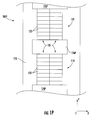
- FIG. 1P is a top view of a photovoltaic module assembly 100P, according to one embodiment.
- the photovoltaic module assembly 100P is similar to the photovoltaic module assembly 100 described above in reference to Figure 1B except that the photovoltaic modules 110 in the photovoltaic module assembly 100P are electrically connected to each other in series and are rotated 90 degrees relative to the photovoltaic modules 110 in the photovoltaic module assembly 100.
- a fabric 170 may include a conductive fabric that has a single conductive element 176P that extends in the Y-direction between the opposing terminals of adjacent photovoltaic modules 110 to make the series connection.
- the photovoltaic module assemblies, such as photovoltaic module assembly 100P include photovoltaic modules connected in series extend for lengths up 20 meters and generate high output voltages, such as on the order of 1 kilovolt (kV).
- FIG. 2A is a cross sectional view of a flexible photovoltaic module assembly 201, according to another embodiment.
- the photovoltaic module assembly 201 is similar to the photovoltaic module assembly 100 described above except that the photovoltaic module assembly 201 includes a fabric 270 having a first conductive layer 271 and a second conductive layer 272 instead of the fabric 170 that includes the first conductive fabric 171 and the second conductive fabric 172.
- the conductive layers 271, 272 can be formed of materials other than fabrics, such as flexible solid conductive sheets (e.g., metal foils).
- the conductive layers 271, 272 can act as a barrier foil for the photovoltaic module assembly 201.
- additional photovoltaic modules 110 can be spaced apart from the photovoltaic module 110 shown in Figure 2A in both the X-direction and the Y-direction.
- the photovoltaic modules 110 spaced apart from each other in the Y-direction can be electrically isolated from each other by removing portions of the conductive layers 271, 272, for example by laser scribing the conductive layers, after placing the conductive layers on the insulating fabric 175.
- the conductive layers 271, 272 may be formed using a process similar to the one discussed in conjunction with Figures 1N-1O .
- FIG. 2B is a cross sectional view of a flexible photovoltaic module assembly 202, according to another embodiment.
- the photovoltaic module assembly 202 is similar to the photovoltaic module assembly 201 described above except that the photovoltaic module assembly 202 includes a fabric 275 having a pair of channels 291, 292 to expose surfaces of respective conductive layers in the photovoltaic assembly 202.
- the photovoltaic module assembly 202 includes a first conductive layer 281 that has a portion 283 that extends to the channel 291.
- the photovoltaic module assembly 202 includes a second conductive layer 282 that has a portion 284 that extends to the channel 292.
- the first channel 291 can extend in the Y-direction substantially perpendicular to the X-direction.
- the channels 291, 292 facilitate making electrical connections to the conductive layers 281, 282.
- the channels 291, 292 can be spaced apart from the photovoltaic sub-modules 120 by enough of a distance so that any moisture or humidity present at the channels will not reach the photovoltaic sub-modules 120.
- the channels 291, 292 can be used to make external electrical connections to the conductive layers 281, 282, such as connecting the conductive layers 281, 282 to a charge controller or other electronics for charging one or more power sources (e.g., a battery bank).
- the channels 291, 292 can be used to connect the conductive layers 281, 282 to other photovoltaic module assemblies to form a larger array of photovoltaic modules 110, such as an array that extends in the X and Y-directions.
- the other photovoltaic module assemblies (not shown) that can connect to the photovoltaic module assembly 202 can have outer portions with protruding conductors (e.g., conductors extending downward) designed to overlap the top surface of the photovoltaic module assembly 202, so that the protruding conductors can fit into the channels 291, 292 and make electrical contact with the conductive layers 281, 282.
- the channels 291, 292 are shown at the top surface of the insulating fabric, in other embodiments the similar channels may be formed at other locations on the photovoltaic module assembly, such as at the bottom surface of the insulating fabric 175 or at one or more of the side surfaces of the insulating channel. Furthermore, in some embodiments, the channels 291, 292 can extend for substantially all of the length of the photovoltaic module assembly 202 in the Y-direction, such as at least 75% of the length of the photovoltaic module assembly 202 in the Y-direction.
- FIG 3A is a cross sectional view of a flexible photovoltaic module assembly 301, according to an example not being part of the present invention.
- the photovoltaic module assembly 301 is similar to the photovoltaic module assembly 100 described above except that the photovoltaic module assembly 301 includes photovoltaic modules 310 disposed on a fabric 370 instead of within a fabric, or between two portions of fabric, such as how the photovoltaic modules 110 are disposed in the recess 173 of the fabric 170 as shown in Figure 1A .
- the photovoltaic module assembly 301 includes a plurality of photovoltaic modules 310 that are disposed on the fabric 370 in a similar arrangement (e.g., modules spaced apart in the Y-direction) to the photovoltaic modules 110 disposed on the fabric 170 shown in Figure 1B .
- Each photovoltaic module 310 can similarly include two or more photovoltaic sub-modules 120 similar to the photovoltaic modules 110 described above.
- the photovoltaic sub-modules 120 of the photovoltaic modules 310 are disposed on the substrate 125.
- the front-side adhesive 140 is disposed over the photovoltaic sub-modules 120, and the front sheet 150 is disposed over the front-side adhesive 140.
- the back-side adhesive 130 in this embodiment is further used to secure the substrate 125 and photovoltaic sub-modules 120 to a back sheet 335.
- the back sheet 335 can be disposed on an outer surface of the back-side adhesive 130, such as a bottom surface of the back-side adhesive 130.
- the back sheet 335 may include a reflective material, such as a metal layer, a reflective polymer or a polymer with a reflective layer (e.g., metal foil) formed over a first surface that is adjacent to the bottom surface of the back-side adhesive 130.
- the back sheet 335 may be formed from a flexible material (e.g., Flexible polymer layer and/or flexible metal foil).
- the back sheet 335 may include a fiber-reinforced polymer material.
- the back sheet 335 may be formed of a rigid or semi-rigid material. The back sheet 335 is secured to the insulating fabric 375 using an adhesive 345.
- Figure 3A shows an adhesive 345 being used to secure the photovoltaic module 310 to the fabric 370, in other examples other techniques may be used, such as sewing.
- An edge seal 360 extends from the front sheet 150 to the back sheet 335 to protect the photovoltaic sub-modules 120 from the external environment.
- the edge seal 360 can be formed of the same materials as the edge seal 160 described above.
- the fabric 370 includes a first conductor 371 and a second conductor 372.
- the first conductor 371 and the second conductor 372 can be formed of a conductive material, such as a metal containing foil, sheet, yarn, wires or other flexible conductive materials as similarly discussed herein.
- the fabric 370 further includes an insulating fabric 375 that can be formed of the same materials as the insulating fabric 175 described above.
- the insulating fabric 375 includes a first surface 377 facing the photovoltaic sub-module 120 and a second surface 378 opposite to the first surface 377.
- the first conductor 371 includes an inner portion 373 extending between two or more photovoltaic cells 123 of the array of the photovoltaic sub-module 120 and the second surface 378 of the insulating fabric 375.
- the second conductor 371 includes an inner portion 374 extending between two or more photovoltaic cells 123 of the array and the second surface 378 of the insulating fabric 375.
- the inner portions 373, 374 can extend under a portion of most or all of the photovoltaic cells 123 allowing the inner portions 373, 374 to serve as a barrier foil for the photovoltaic sub-module 120.
- the back sheet 335 can be omitted.
- a porous conductive layer such as the conductive mesh 178M described above, is used for the conductors 371, 372, then it may be preferable to include the back sheet 335.
- a back sheet can be placed outward of the conductive layer (i.e., the conductive layer can be disposed between the photovoltaic modules and the back sheet).
- a bypass diode 199 described above in reference to Figure 1A can be connected between the inner portion 373 of the first conductor 371 and the inner portion 374 of the second conductor 372.
- the spacing between the inner portion 373 of the first conductor 371 and the inner portion 374 of the second conductor 372 can be designed so that the diode 199 can be directly connected to the inner portions 373, 374.
- the conductors 371, 372 can serve as barrier foils and the bypass diode 199 may be connected to the conductors without any additional wiring.
- the conductors 371, 372 can further include a respective protruding portion 376, 379 extending through the insulating fabric 375, the adhesive 345, the back sheet 335, the edge seal 360, and the front-side adhesive 340 to connect to the respective ends 121, 122 of the photovoltaic sub-module 120.
- the photovoltaic modules 310 are placed on the fabric 370, and then the edge seal 360 is added to encapsulate the protruding portions 376, 379 of the respective conductors 371, 372 and at least a portion of the photovoltaic modules 310.
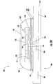
- FIG 3B is a cross sectional view of a flexible photovoltaic module assembly 302, according to another example not being part of the present invention.
- the photovoltaic module assembly 302 is similar to the photovoltaic module assembly 301 described above except that the photovoltaic module assembly 302 includes a junction box 350 that is used to electrically connect the photovoltaic sub-module(s) 120 to the conductors of a fabric 380 to which the photovoltaic sub-module 120 is mounted.
- the fabric 380 is similar to the fabric 370 described above in reference to Figure 3A except that the fabric 380 includes different conductors.
- the fabric 380 includes conductors 381, 382 that are routed through the junction box 350.
- the junction box 350 can be attached to a surface 337 (e.g., a lower surface) of the back sheet 335 facing away from the photovoltaic sub-module 120.
- the back sheet 335 includes an opening 336 for routing the conductors 381, 382 to the photovoltaic sub-module 120.
- the conductors 381, 382 extend from the fabric 380 into the junction box 350, through the opening in the back sheet 335, through the back-side adhesive 130, through the edge seal 360 and front-side adhesive 140 and to the separate ends 121, 122 of the photovoltaic sub-module 120.
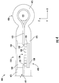
- a photovoltaic module 303 includes a junction box 350 located at an opening through the back sheet 335 which can be mechanically attached to a fabric 170 that has a pair of conductors (e.g., conductive fabrics 171, 172) for connecting to the opposing ends 121, 122 of the photovoltaic modules 110.
- the opposing ends 121, 122 of the photovoltaic module 110 can be connected by use of two or more conduction pins 391 (e.g., metal pins, rods, etc.) that extend within the junction box 350.
- the conduction pins 391 can be inserted through a first side of the fabric 170 to make electrical contact with the conductors in the fabric 170.
- a plate 392 on an opposing second side of the fabric 170 can be fastened to the junction box 350 by use of fastener 393 to secure the photovoltaic module(s) to the fabric 170.
- the fasteners 393 can extend through the insulating material of the fabric 170 and holes 394 formed within conductive elements within the fabric 170 to connect to the junction box 350 to the fabric 170.
- a threaded fastener may fastened to internal threads formed in the junction box 350. This example allows the photovoltaic modules and the fabric having the internal conductors to be separately formed and then quickly connected to each other.
- the use of fasteners 393 allows easy replacement of a photovoltaic module assembly.
- FIG. 3D is a top view of a photovoltaic module assembly 301D, according to one example not being part of the present invention.
- the photovoltaic module assembly 301D is similar to the photovoltaic assembly 301 described above except that a different fabric is used and different components are used to make the electrical connection between the conductor in the fabric and the array of photovoltaic cells 123.
- the photovoltaic module assembly 301D includes the fabric 170h described above. This embodiment of the fabric 170h includes the bottom insulating layer 175B and the top insulating layer 175A.
- the fabric 170h may further include holes 376h through the top insulating layer 175A so as to expose a portion of the conductors 178.
- the photovoltaic module assembly 301D further includes a busbar 388 that is electrically connected to an end of the array of photovoltaic cells 123 in a sub-module.
- a conductive adhesive 385 can then be disposed so that it extends between the busbar 388 and the conductor 178 disposed in the fabric 170h to electrically connect the busbar 388 and the conductor 178.
- Corresponding holes can be added to other layers (e.g., the back sheet 335) in the photovoltaic module assembly 301 D to create a conductive path between the busbar 388 and the conductor 178 in the fabric 170h through the conductive adhesive 385.
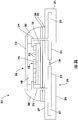
- FIG 4 is a cross sectional view of a flexible photovoltaic module assembly 400, according to another embodiment.
- the photovoltaic module assembly 400 is similar to the photovoltaic module assembly 201 described above except that the photovoltaic module assembly 400 includes a keder 450 at one end of the photovoltaic module assembly 400 in the X-direction.
- the photovoltaic module assembly 400 may also include additional photovoltaic modules 110 (not shown) that are spaced apart from the photovoltaic module 110 shown in Figure 4 in the X-direction and/or the Y-direction.
- the keder 450 can be used to secure or mount the photovoltaic module assembly 400 to another structure.
- the keder 450 can be positioned in a corresponding groove or other fixation profile (not shown) for mounting the photovoltaic module assembly 400 to a wall, building, building façade or other similar structure.
- the photovoltaic module assembly 400 includes a fabric 470 that is similar (e.g., similar materials for the conductive layers and insulating fabric) to the fabric 270 described above in reference to Figures 1N-1O and 2A .
- the fabric 470 includes a first conductive layer 471 and a second conductive layer 472.
- the first conductive layer 471 extends from the first end 121 of the photovoltaic sub-module 120 towards another photovoltaic module 110 (not shown).
- the second conductive layer 472 extends from the second end 122 of the photovoltaic sub-module 120 to the keder 450.
- the keder 450 includes a core 455 that can be formed of a conductive material, such as rigid conductive material (e.g., a metal tube or bar).
- the second conductive layer 472 can be disposed around the core 455 to make contact with the core 455.
- Insulating fabric 475 which is similar to at least a portion of the insulating fabric 175 described above, can surround the second conductive layer 472 and the core 455 to form the outer portion of the keder 450.
- the core 455 can be electrically connected to external equipment, such as a charge controller or other electronics to charge a power source (e.g., a battery bank).
- the core 455 formed of a rigid, conductive material can provide mechanical strength to secure the photovoltaic module assembly 400 to the corresponding receiving element, groove or other fixation profile (not shown) and also form part of the electrical circuit connected to the photovoltaic sub-module 120.
- keders 450 e.g., a keder 450 at either end of the photovoltaic module assembly 400 in the X-direction
- use of one or more keders 450 built into the photovoltaic module assembly 400 can increase the speed at which the photovoltaic module assembly 400 is installed to form a roof, facade, wall, or other structure as the one or more keders 450 can reduce the process of mounting the photovoltaic module assembly 400 to simply inserting the keders 450 into one or more corresponding receiving element, groove or other fixation profile.
Landscapes
- Engineering & Computer Science (AREA)
- General Physics & Mathematics (AREA)
- Physics & Mathematics (AREA)
- Condensed Matter Physics & Semiconductors (AREA)
- Electromagnetism (AREA)
- Computer Hardware Design (AREA)
- Microelectronics & Electronic Packaging (AREA)
- Power Engineering (AREA)
- Life Sciences & Earth Sciences (AREA)
- Chemical & Material Sciences (AREA)
- Crystallography & Structural Chemistry (AREA)
- Sustainable Energy (AREA)
- Sustainable Development (AREA)
- Photovoltaic Devices (AREA)
Description
- Embodiments of the present disclosure generally relate to a flexible photovoltaic apparatus.
- Photovoltaic apparatuses have conventionally employed a rigid layer of crystalline silicon as the active photovoltaic layer in the apparatus. More recently, thin-film photovoltaic apparatuses using flexible photovoltaic layers, such as layers of Cu(In,Ga)Se2 semiconductor also known as CIGS, have been developed to compete with conventional photovoltaic apparatuses. To extract electrical power from both conventional and thin-film photovoltaic apparatuses, flat and rigid busbars are frequently connected between the photovoltaic devices in the photovoltaic apparatus and a junction box mounted to the photovoltaic apparatus. Providing an electrical connection to a photovoltaic apparatus through the use of flat and rigid busbars and a junction box is a time consuming and inefficient process that often requires one or more manual steps or specialized equipment to automate. Also, the more electrical connections within an electrical circuit in a photovoltaic apparatus, typically the greater the series resistance in the electrical circuit (e.g., contact resistance issues) and the less reliable and repeatable the formed electrical circuit is, which can lead to production yield and lifetime issues of the formed photovoltaic device.
- Advantageously, thin-film photovoltaic apparatuses can largely be manufactured using a roll to roll process in which layers are sequentially added over a flexible substrate and then the finished product can be wound into a roll simplifying storage and transport of the apparatus.
US 2011/290304 ,US 4 537 838 ,US 2010/154857 andWO 2008/ 134677 disclose photovoltaic devices arranged on flexible insulating fabrics. Despite the benefits of using a roll-to-roll process, thin-film photovoltaic apparatuses have continued to use junction boxes and rigid busbars to make electrical connections due to the reliability of these electrical connections and because junction boxes can effectively be sealed to prevent moisture from damaging the interior components of the photovoltaic apparatuses. - Therefore, there is a need for an improved photovoltaic apparatus that provides electrical connections within the photovoltaic apparatus and to external equipment without the use of rigid busbars or junction boxes while still preventing moisture from damaging the interior components of the photovoltaic apparatus.
- Embodiments of the present disclosure generally relate to an apparatus having one or more photovoltaic devices disposed on a flexible supporting material. In one embodiment, a flexible photovoltaic apparatus is provided including a photovoltaic device that includes an array of photovoltaic cells having a first end and a second end. The array extends in a first direction from the first end to the second end. The photovoltaic apparatus further includes a first fabric that includes an insulating fabric, a first conductor disposed in or on the insulating fabric and connected to the first end of the array, and a second conductor disposed in the insulating fabric and connected to the second end of the array. The photovoltaic device is disposed within the insulating fabric.
- So that the manner in which the above recited features of the present disclosure can be understood in detail, a more particular description of the disclosure, briefly summarized above, may be had by reference to embodiments, some of which are illustrated in the appended drawings. It is to be noted, however, that the appended drawings illustrate only exemplary embodiments and are therefore not to be considered limiting of its scope, and may admit to other equally effective embodiments.
-
Figure 1A is a cross sectional view of a flexible photovoltaic module assembly, according to one embodiment. -
Figure 1B is a top view of the photovoltaic module assembly ofFigure 1A taken at a level in the Z-direction of theline 1B inFigure 1A . -
Figure 1C is an isometric view of a portion of a fabric that may be disposed within a flexible photovoltaic module assembly, according to one embodiment. -
Figure 1D is a side cross-sectional view of a portion of the fabric illustrated inFigure 1C , according to one embodiment. -
Figure 1E is an isometric view of a portion of a fabric that may be disposed within a flexible photovoltaic module assembly, according to one embodiment. -
Figure 1F is a side cross-sectional view of a portion of the fabric illustrated inFigure 1E , according to one embodiment. -
Figure 1G is a side cross-sectional view of an alternate configuration of a portion of the fabric illustrated inFigure 1E , according to one embodiment. -
Figure 1H is a side view of a fabric that may be disposed within a flexible photovoltaic module assembly, according to one embodiment. -
Figure 1I is a partial top view of a fabric that may be disposed within a flexible photovoltaic module assembly, according to one embodiment. -
Figure 1J is a partial side view of a fabric that may be disposed within a flexible photovoltaic module assembly, according to one embodiment. -
Figure 1K is a partial side view of a fabric that may be disposed within a flexible photovoltaic module assembly, according to one embodiment. -
Figure 1L is a partial side view of a fabric that may be disposed within a flexible photovoltaic module assembly, according to one embodiment. -
Figure 1M is a top view of afabric 170 that may be disposed within a flexible photovoltaic module assembly, according to one embodiment. -
Figure 1N is a plan view of a portion of a conductive fabric sheet that has been sectioned to form two electrically isolated conductive fabrics, according to one embodiment. -
Figure 1O is a side cross-sectional view of the portion of the conductive fabric sheet illustrated inFigure 1N , according to one embodiment. -
Figure 1P is a top view of a photovoltaic module assembly, according to one embodiment. -
Figure 2A is a cross sectional view of a flexible photovoltaic module assembly, according to another embodiment. -
Figure 2B is a cross sectional view of a flexible photovoltaic module assembly, according to another embodiment. -
Figure 3A is a cross sectional view of a flexible photovoltaic module assembly, according to an example not being part of the present invention. -
Figure 3B is a cross sectional view of a flexible photovoltaic module assembly, according to another embodiment. example not being part of the present invention. -
Figure 3C is a cross sectional view of a flexible photovoltaic module assembly, according to another example not being part of the present invention. -
Figure 3D is a cross sectional view of a flexible photovoltaic module assembly, according to another example not being part of the present invention. -
Figure 4 is a cross sectional view of a flexible photovoltaic module assembly, according to another embodiment. - To facilitate understanding, identical reference numerals have been used, where possible, to designate identical elements that are common to the figures. It is contemplated that elements and features of one embodiment may be beneficially incorporated in other embodiments without further recitation.
- Embodiments of the present disclosure generally relate to an apparatus having one or more photovoltaic devices disposed on a flexible supporting material. Embodiments of the present disclosure may also relate to an apparatus and method of forming a photovoltaic module assembly that includes a plurality of photovoltaic modules and a flexible supporting material that has one or more integrated conductive elements disposed therein that is used to interconnect the plurality of photovoltaic modules.
-
Figure 1A is a cross sectional view of a flexible photovoltaic module assembly 100 (flexible photovoltaic apparatus), according to one embodiment of the disclosure provided herein.Figure 1B is a top view of thephotovoltaic module assembly 100 taken at a level in the Z-direction of theline 1B inFigure 1A . Thephotovoltaic module assembly 100 may include multiple optoelectronic devices, such as photovoltaic devices (e.g., solar cells), diodes, and LEDs. The view inFigure 1B of thephotovoltaic module assembly 100 is shown including twophotovoltaic modules 110 although morephotovoltaic modules 110 may be included as thephotovoltaic module assembly 100 extends in the Y-direction (second direction). Eachphotovoltaic module 110 will generally include two or more photovoltaic sub-modules 120 (photovoltaic device), although fewerphotovoltaic sub-modules 120 may be included in some configurations. - The
photovoltaic modules 110 is disposed within a fabric 170 (first fabric). Thefabric 170 serves as the supporting material for thephotovoltaic modules 110 and typically also provides one or more of the electrical connections to thephotovoltaic modules 110. For example, thefabric 170 includes a first conductive fabric 171 (first conductor) and a second conductive fabric 172 (second conductor) that are electrically connected toopposing ends photovoltaic sub-module 120. In some embodiments, the conductive elements in the firstconductive fabric 171 and the secondconductive fabric 172 are directly electrically connected to conductive regions formed at theopposing ends photovoltaic sub-module 120, and thus remove the need for traditional busbars disposed at each of theopposing ends conductive fabrics insulating fabric 175. -
Figures 1C-1G illustrate examples of configurations of afabric 170 that may be used in thephotovoltaic module assembly 100.Figure 1C is an isometric view of a portion of a fiber containing version of thefabric 170.Figure 1D is a side view that is aligned with aconductive fiber 171A in a portion of thefabric 170 shown inFigure 1C . In general, thefabric 170 may contain a topinsulating layer 175A, aconductive fabric 171 and abottom insulating layer 175B. Theconductive fabric 171 may include a plurality of conductive elements, such asconductive fibers 171A, and a plurality of electrically insulatingfibers 171B that are bonded and/or woven together. Theconductive fibers 171A include conductive current carrying elements, such as metal wires (e.g., wires containing copper, silver, tin, lead, gold, and/or aluminum), conductive yarns or other flexible conductive materials (e.g., graphite fibers). In some embodiments, theconductive fibers 171A include a non-conductive fabric that is coated with a conductive material (e.g., a non-conductive fabric coated with a metal, such as aluminum, silver or copper). The non-conductive material used to form these coated conductive fabrics can include fabrics formed of, for example, ethylene tetrafluoroethylene (ETFE), polytetrafluoroethylene (PTFE), polyvinyl chloride (PVC), thermoplastic olefins (TPO), or composites (e.g., composites with glass fibers). One or more of theconductive fibers 171A in theconductive fabric 171 may be aligned or oriented in one or more directions (e.g., X and/or Y-directions) within theconductive fabric 171 to interconnect one or more of the electrical components (e.g., photovoltaic modules 110) within thephotovoltaic module assembly 100. Referring toFigure 1C , in some configurations, two or moreconductive fibers 171A may be oriented such that they can conduct electricity in a first direction (X-direction) and the insulatingfibers 171B, which are used to support theconductive fibers 171A, may be positioned (e.g., woven together) such that they extend in the first direction and/or a second direction (Y-direction). The top insulatinglayer 175A and the bottom insulatinglayer 175B may include a non-porous insulating sheet, polymer impregnated insulating woven fabric or other insulating material that can physically isolate the conductive elements in theconductive fabric fabric 170. In some examples, the top insulatinglayer 175A and the bottom insulatinglayer 175B comprise a polymer material or insulating fiber material, such as a material that may include ETFE, ECTFE, PTFE, PVC, TPO, glass, Nylon, or epoxy. -
Figure 1E is an isometric view of a portion of an alternate type offabric 170.Figures 1F and 1G are side views of two different examples of thefabric 170 illustrated inFigure 1E . In these examples, the portion of thefabric 170 includes the top insulatinglayer 175A, theconductive fabric 171 and the bottom insulatinglayer 175B. However, in one configuration, as shown inFigure 1F , theconductive fabric 171 may include a conductive material containing layer (e.g.,conductive layer 171C) that at least partially extends in a first direction (e.g., X-direction) and/or a second direction (e.g., Y-direction). In one example, theconductive layer 171C within theconductive fabric 171 includes a flexible metal foil or flexible conductive sheet that is configured to transfer current between two or morephotovoltaic modules 110. In some configurations, theconductive layer 171C is metal containing layer that is patterned to form separate conductive regions that are electrically isolated from each other and are aligned or oriented so as to transfer current between the various electrical components (e.g., photovoltaic modules 110) within thephotovoltaic module assembly 100. In one configuration, as shown inFigure 1G , one of the insulating layers, such as the bottom insulatinglayer 175B further includes a reinforcement layer 175C. The reinforcement layer 175C may include a fiber containing textile, woven fabric or other reinforcing material that is adapted to provide mechanical support tofabric 170. - Therefore, by aligning and configuring the one or more conductive elements within the
conductive fabrics fabric 170, various photovoltaic module interconnection configurations can be achieved. Referring toFigure 1B , in some embodiments, theconductive fabric 171 includes conductive elements (e.g.,conductive fibers 171A,conductive layers 171C) that are configured to conduct electricity in at least the +Y and -Y-directions to interconnect the opposing ends 121 of two or morephotovoltaic modules 110, and theconductive fabric 172 includes conductive elements that are configured to conduct electricity in at least the +Y and -Y-directions to interconnect the opposing ends 122 of the two or morephotovoltaic modules 110. Examples of other interconnection configurations are further discussed below. WhileFigure 1B illustrates thephotovoltaic modules 110 being electrically connected in parallel using theconductive fabrics photovoltaic modules 110 may be electrically connected in series. - In other embodiments, one or more conductors may be disposed onto one or more fabrics.
Figure 1H is a side view of afabric 170h that may be disposed within a flexible photovoltaic module assembly, according to one embodiment. Thefabric 170h includes the bottom insulatinglayer 175B, which can be an insulating fiber material as described above. In this embodiment,conductors 178 can be placed directly onto the bottom insulatinglayer 175B. Theconductors 178 can be placed onto the bottom insulatinglayer 175B in a desired pattern and orientation so as to interconnect two or more photovoltaic modules. In one example, theconductors 178 are configured to conduct electricity in at least the +Y and -Y-directions to interconnect two or morephotovoltaic modules 110 that are disposed in an array that extends in the Y-direction. In one embodiment, theconductors 178 can be placed onto the bottom insulatinglayer 175B using methods, such as sputtering or screen printing a conductive material, such as a metal (e.g., copper, silver, tin, aluminum), or depositing an organic conductor onto a surface of the bottom insulating layer. In another embodiment, theconductors 178 can be placed onto the bottom insulatinglayer 175B by laminating or bonding a conductive strip, sheet or wire thereon, such as a metal containing strip (e.g., copper, silver, tin, or aluminum containing strip). The electrically separatedconductors 178 can be used to make electrical connections (e.g., connections of opposite polarity) to the photovoltaic sub-modules (not shown). Although not shown, in some embodiments, at least a portion of the top insulatinglayer 175A can be placed over the bottom insulatinglayer 175B after theconductors 178 are placed onto the bottom insulatinglayer 175B. -
Figure 1I is a partial top view of afabric 170i that may be disposed within a flexible photovoltaic module assembly, according to one embodiment. Thefabric 170i is similar to thefabric 170h described above except that thefabric 170i hasconductors 178 that extend in two dimensions across a surface of the bottom insulatinglayer 175B to form amesh 178M ofconductors 178. Theconductors 178 shown in themesh 178M on the bottom insulatinglayer 175B of thefabric 170i can be used to make electrical connections to photovoltaic modules (not shown) that are disposed in an array that extends in the X and/or Y-directions. Electrically separatedmeshes 178M can be used to make electrical connections (e.g., connections of opposite polarity) to the photovoltaic sub-modules (not shown). Themesh 178M can be formed using the same methods described above for theconductors 178 in reference toFigure 1H . -
Figure 1J is a partial side view of afabric 170j that may be disposed within a flexible photovoltaic module assembly, according to one embodiment. Thefabric 170j includes the bottom insulatinglayer 175B, which can be an insulating fiber material as described above. In this embodiment,conductive threads 177 can be partially or fully (i.e., fully surrounded by insulating fabric) disposed within the bottom insulatinglayer 175B. In other embodiments, theconductive threads 177 can be disposed on the insulatinglayer 175B. For example, theconductive threads 177 can be placed on the insulatinglayer 175 and then an adhesive or a lamination process can be used to secure theconductive threads 177 to the insulatinglayer 175B. The electrically separated and oriented regions that contain theconductive threads 177 can be used to make electrical connections (e.g., connections of opposite polarity) to the photovoltaic sub-modules (not shown). In one example, the regions that contain theconductive threads 177 are configured to conduct electricity in at least the +Y and -Y-directions to interconnect two or morephotovoltaic modules 110, which are disposed in an array that extends in the Y-direction. Although not shown, in some embodiments, the top insulatinglayer 175A can be placed over the bottom insulatinglayer 175B after theconductive threads 177 are placed onto or disposed within the bottom insulatinglayer 175B. Theconductive threads 177 can be formed of a conductive material, such as a metal containing yarn, wires or other flexible conductive materials as similarly discussed herein. -
Figure 1K is a partial side view of afabric 170k that may be disposed within a flexible photovoltaic module assembly, according to one embodiment. Thefabric 170k includes the bottom insulatinglayer 175B and the top insulatinglayer 175A, which can be an insulating fiber material as described above. In this embodiment, aconductive layer 176 is disposed between the insulatinglayers conductive layer 176 can be formed of one of the conductive materials described above, including but not limited to theconductors 178, theconductive mesh 178M, or theconductive threads 177. Electrically separatedconductive layers 176 can be used to make electrical connections (e.g., connections of opposite polarity) to the photovoltaic sub-modules (not shown). -
Figure 1L is a partial side view of afabric 170L that may be disposed within a flexible photovoltaic module assembly, according to one embodiment. Thefabric 170L includes the bottom insulatinglayer 175B and the top insulatinglayer 175A, which can be an insulating fiber material as described above. Thefabric 170L further includes an additional middle insulatinglayer 175M that may be formed of the same materials as the insulatinglayers layer 175M may be disposed between the bottom insulatinglayer 175A and the top insulatinglayer 175A. In this embodiment, aconductive layer 176 is disposed between the insulatinglayers layers conductive layer 176 can be formed of one of the conductive materials described above, including but not limited to theconductors 178, theconductive mesh 178M, or theconductive threads 177. In some embodiments, theconductive layers 176 shown inFigure 1L can be electrically separatedconductive layers 176 that can be used to make electrical connections (e.g., connections of opposite polarity) to the photovoltaic sub-modules (not shown). Other embodiments of fabrics that may be used within a flexible photovoltaic module assembly may include more than twoconductive layers 176 that are spaced apart in the Z-direction by an insulating layer. -
Figure 1M is a top view of afabric 170m that may be disposed within a flexible photovoltaic module assembly, according to one embodiment. The fabric 175m includes a pair ofconductive layers 176 spaced apart in the Y-direction. Theconductive layers 176 are shown with dashed lines to indicate that theconductive layers 176 are hidden beneath the top insulatinglayer 175A. Thefabric 170m includes a modified top insulatinglayer 175A that includes a plurality ofholes 175h. The plurality ofholes 175h can be used to enable electrical connections (e.g., connections of opposite polarity) to be formed between specific connection points on the photovoltaic modules (not shown) and a portion of theconductive layer 176. For example, photovoltaic modules, having conductive pins or other conductors disposed thereon, can be placed on thefabric 170m, so that the conductive pins are aligned with theholes 175h, and thus the conductive pins can make electrical contact with a desired portion of aconductive layer 176. In some embodiments, the pattern of theholes 175h that are formed in the insulating layer can be configured to match a specific pattern of the connecting pins disposed on each photovoltaic module. Thus, by the selection of a desirable hole pattern in the insulating layer the positional alignment of a photovoltaic module can be set such that it prevents improper installation of the photovoltaic module on the fabric and properly aligns the photovoltaic module within the photovoltaic module assembly. - In some embodiments, each
photovoltaic sub-module 120 is formed on asubstrate 125. Thesubstrate 125 may be a flexible substrate, a rigid substrate, or semi-rigid material containing substrate (i.e., semi-rigid substrates distort under their own weight, but are unable to be wound into a roll), and is typically formed from an electrically insulating material. For example, in one embodiment a polyimide substrate may be used for thesubstrate 125. - In some embodiments, each
photovoltaic sub-module 120 within eachphotovoltaic module 110 may include a plurality of thin-film layers that are deposited on thesubstrate 125, and then patterned (e.g., scribed) to form a plurality of monolithically interconnectedphotovoltaic cells 123 that are electrically connected in series in an array. The array extends in the X-direction (first direction) from afirst end 121 of the photovoltaic sub-module 120 to asecond end 122 of thephotovoltaic sub-module 120. In other embodiments, thephotovoltaic sub-modules 120 can include a photovoltaic device formed on another substrate that is then positioned on thesubstrate 125. - Each photovoltaic sub-module 120 can be formed of, for example, a back-contact layer (not shown) formed on the
substrate 125, an absorber layer (not shown) formed over the back-contact layer, and a front-contact layer (not shown) formed over the absorber layer. The back-contact layer can be fabricated from a material having a high optical reflectance and is commonly made of molybdenum (Mo) although several other thin-film materials, such as metal chalcogenides, molybdenum chalcogenides, molybdenum selenides (such as MoSe2), sodium (Na)-doped Mo, potassium (K)-doped Mo, Na- and K-doped Mo, transition metal chalcogenides, tin-doped indium oxide (ITO), doped or non-doped indium oxides, doped or non-doped zinc oxides, zirconium nitrides, tin oxides, titanium nitrides, titanium (Ti), tungsten (W), tantalum (Ta), gold (Au), silver (Ag), copper (Cu), and niobium (Nb) may also be used or included advantageously. In some embodiments, the back-contact layer is deposited onto thesubstrate 125 by use of sputtering process. - The absorber layer is typically made of an "ABC" material, wherein "A" represents elements in group 11 of the periodic table of chemical elements as defined by the International Union of Pure and Applied Chemistry including copper (Cu) or silver (Ag), "B" represents elements in group 13 of the periodic table including indium (In), gallium (Ga), or aluminum (Al), and "C" represents elements in group 16 of the periodic table including sulfur (S), selenium (Se) or tellurium (Te). An example of an ABC material is the Cu(In,Ga)Se2 semiconductor also known as CIGS. In some embodiments, the absorber layer may be a polycrystalline material. In other embodiments, the absorber layer may be a monocrystalline material. Another example of a material that may be used as the absorber layer is chalcopyrite.
- The front-contact layer can be an electrically conductive and optically transparent material, such as a transparent conductive oxide (TCO) layer. For example, in some embodiments, the front-contact layer may be formed of doped or non-doped variations of materials, such as indium oxides, tin oxides, or zinc oxides.
- In some embodiments, a semiconductive buffer layer can be disposed between the absorber layer and the front-contact layer. The semiconductive buffer layer ordinarily has an energy bandgap higher than 1.5 eV. The semiconductive buffer layer may be formed of materials, such as CdS, Cd(S,OH), CdZnS, indium sulfides, zinc sulfides, gallium selenides, indium selenides, compounds of (indium, gallium)-sulfur, compounds of (indium, gallium)-selenium, tin oxides, zinc oxides, Zn(Mg,O)S, Zn(O,S) material, or variations thereof.
- Each
photovoltaic module 110 may be encapsulated within thephotovoltaic module assembly 100 by use of a front-side adhesive 140 and a back-side adhesive 130. In some embodiments, the front-side adhesive 140 and the back-side adhesive 130 completely surround and encapsulate thephotovoltaic sub-modules 120. The front-side adhesive 140 can be formed over the front-contact layer of each of thephotovoltaic sub-modules 120, and also over portions of theconductive fabrics 171, 172 (described in greater detail below) that make electrical connections to thephotovoltaic sub-modules 120. The front-side adhesive 140 may be formed of a flexible material, such as a flexible polymer. For example, in one embodiment the front-side adhesive 140 may be formed of a thermoplastic olefin (TPO) based polymer or a TPO blend. - The back-
side adhesive 130 is disposed over the side of thesubstrate 125 that is opposite to the side that thephotovoltaic sub-module 120 is formed. The back-side adhesive 130 may be formed of a flexible material, such as a flexible polymer. For example, in one embodiment the back-side adhesive 130 may be formed of a thermoplastic olefin-based polymer (TPO) or a TPO polymer blend. The back-side adhesive 130 may also be disposed on, over or around portions of theconductive fabrics 171, 172 (described in greater detail below). The back-side adhesive 130 may contact the front-side adhesive 140 at one or more locations, such as edges 111 of thephotovoltaic modules 110 in the Y-direction, so that the front-side adhesive 240 and the back-side adhesive 230 can protect these areas of thephotovoltaic modules 110 from the external environment. - A
front sheet 150 can be disposed on an outer surface of the front-side adhesive 140, such as a top surface of the front-side adhesive 140. Thefront sheet 150 can be formed of a transparent material, such as glass or a transparent thermoplastic polymer. Thefront sheet 150 may be formed of an optically transparent flexible material. - In some embodiments, each
photovoltaic module 110 can further include an optional edge seal 160 (Figure 1A ) disposed around the edges of eachphotovoltaic sub-module 120. The presence of theedge seal 160 at the edge of thephotovoltaic module assembly 100 can help assure thatphotovoltaic module assembly 100 can eliminate common photovoltaic apparatus manufacturing and photovoltaic device failure modes by preventing moisture and other substances from reaching thephotovoltaic sub-modules 120. In some embodiments, theedge seal 160 can be formed over the outer surface of thefront sheet 150 as well to provide an even stronger seal against the external environment. In general, theedge seal 160 comprises a polymeric material, such as an elastomer, for example a butyl rubber. - As noted above, the first
conductive fabric 171 is connected to thefirst end 121 of thephotovoltaic sub-module 120, and the secondconductive fabric 172 is connected to thesecond end 122 of thephotovoltaic sub-module 120. In some embodiments, theconductive fabrics ends photovoltaic sub-modules 120, respectively. A conductive adhesive or solder can be used to attach the conductive elements of theconductive fabric ends photovoltaic sub-modules 120. Although the conductive fabrics are shown as contacting the top side (i.e., the side facing the sun during use) of thephotovoltaic sub-module 120, in other embodiments one or both of theconductive fabrics photovoltaic sub-module 120. - The insulating
fabric 175 that at least partially surrounds theconductive fabrics non-conductive material 171B included in theconductive fabrics fabric 175 in some cases may include a silicone containing foam material that is flexible. In some embodiments, the conductive elements in theconductive fabrics fabric 175, while in other embodiments the conductive elements in the conductive fabrics can be attached to the insulating fabric using an adhesive or ultrasonic welding. The insulatingfabric 175 can electrically isolate electrical components disposed in thefabric 170 and can also serve as a moisture barrier to protect thephotovoltaic modules 110. In some embodiments, a portion of the insulatingfabric 175 can be laminated and/or bonded directly to thefront sheet 150 to form a seal around thephotovoltaic modules 110 within thephotovoltaic module assembly 100, thus in some cases removing the need for theedge seal 160. - In some embodiments, one or more
conductive fibers 171A in theconductive fabric 171 configuration may also be used to join thefabric 170 to thephotovoltaic modules 110. In this case, theconductive fibers 171A may be formed in zigzag, straight seam or double straight seam pattern to physically connect portions of thefabric 170 to thephotovoltaic modules 110. Theconductive fibers 171A may be formed in zigzag, straight seam or double straight seam pattern that is primarily aligned parallel to the X and Z-direction (Figure 1A ). In an alternate configuration, theconductive fibers 171A may be formed in zigzag, straight seam or double straight seam pattern that is aligned parallel to the X-Y plane (Figure 1A ). - Using
conductive fabrics fabric 170 instead of flat and rigid busbars as the conductors allows electrical connections to be made to thephotovoltaic sub-modules 120 without sacrificing the flexibility of thefabric 170. Also, in some embodiments, theconductive fabrics - Disposing
photovoltaic modules 110 on flexible materials, such as fabrics, allows thephotovoltaic module assembly 100 to be easily placed on surfaces, such as roofs, building facades or walls, or to span supporting structures to form structures, such as roofs, walls, or shading structures. Placing thephotovoltaic modules 110 on fabrics also reduces the weight of thephotovoltaic module assembly 100 relative to other heavier supporting materials. Moreover, the ease at which fabrics can be placed into a roll simplifies transport and storage of thephotovoltaic module assembly 100. - The
photovoltaic module assembly 100 can be formed by using a roll-to-roll process that includes placing thephotovoltaic modules 110 in or on thefabric 170. For example, to form thefabric 170, the material that forms theconductive fabrics layer 175B), and then an additional layer of insulating fabric 175 (e.g., top insulatinglayer 175A) can be placed over the conductive material. One or more adhesives may be used to secure the conductive material to the insulating material. - In some embodiments, portions of the conductive material (e.g.,
conductive layer 171C inFigures 1E-1G ) are removed before adding the second insulating layer to form the separate conductive fabrics, such as theconductive fabrics conductive fabrics Figures 1N-1O. Figure 1N is a plan view of a formed conductive fabric sheet that has been partially sectioned to form theconductive fabrics conductive fabrics conductive layer 171C, such as by forming agroove 179 in theconductive layer 171C, to electrically separate the conductive regions of theconductive fabrics Figure 1O is a side view of the portion of the partially sectioned portion of the conductive fabric sheet shown inFigure 1N . - During manufacturing, a
photovoltaic module 110 can be added to aphotovoltaic module assembly 100, by positioning it in a recess 173 (Figure 1A ) formed in thefabric 170, and then thephotovoltaic module 110 can be placed in therecess 173. Next, the adhesives, such as the back-side adhesive 130, can be used to secure thephotovoltaic module 110 to thefabric 170 disposed in therecess 173. In some embodiments, a lamination process is used to assist in adhering thephotovoltaic modules 110 to thefabric 170. The lamination process can also assist in adhering the insulatingfabric 175 to theconductive fabrics conductive fabrics photovoltaic module assembly 100 can be combined with one or more otherphotovoltaic module assemblies 100 using techniques, such as sewing or ultrasonic welding to create larger photovoltaic arrays that contain a plurality ofphotovoltaic modules 110 On the outer surfaces of thephotovoltaic module assembly 100, such as surfaces of the insulatingfabric 175, one or more logos, text or other graphics may be added. - The
photovoltaic module assembly 100 may further include one ormore bypass diodes 199, such as flattened bypass diodes, that are designed to prevent the effects of hot-spot heating. For example, in some embodiments, eachphotovoltaic module 110 or eachphotovoltaic sub-module 120 can include abypass diode 199. Thebypass diode 199 can be integrated within thefabric 170 of thephotovoltaic module assembly 100 during manufacturing and is connected in parallel, but with an opposite polarity to the sub-modules 120 as shown inFigure 1A . In some configurations, the leads of abypass diode 199 are electrically connected to the first and secondconductive fabrics bypass diode 199 can be disposed between the conductive fabrics that are formed from a conductive fabric sheet, as illustrated inFigure 1N . In some embodiments, additional electronics can be incorporated into thefabric 170, such as switches, additional diodes, light-emitting diodes, resistors, power optimizers, micro-inverters, or other power electronics. In some embodiments, these additional electronics can be disposed on a structure similar to a printed circuit board within thefabric 170. -
Figure 1P is a top view of aphotovoltaic module assembly 100P, according to one embodiment. Thephotovoltaic module assembly 100P is similar to thephotovoltaic module assembly 100 described above in reference toFigure 1B except that thephotovoltaic modules 110 in thephotovoltaic module assembly 100P are electrically connected to each other in series and are rotated 90 degrees relative to thephotovoltaic modules 110 in thephotovoltaic module assembly 100. In this embodiment, afabric 170 may include a conductive fabric that has a singleconductive element 176P that extends in the Y-direction between the opposing terminals of adjacentphotovoltaic modules 110 to make the series connection. In some embodiments, the photovoltaic module assemblies, such asphotovoltaic module assembly 100P, include photovoltaic modules connected in series extend for lengths up 20 meters and generate high output voltages, such as on the order of 1 kilovolt (kV). -
Figure 2A is a cross sectional view of a flexiblephotovoltaic module assembly 201, according to another embodiment. Thephotovoltaic module assembly 201 is similar to thephotovoltaic module assembly 100 described above except that thephotovoltaic module assembly 201 includes afabric 270 having a firstconductive layer 271 and a secondconductive layer 272 instead of thefabric 170 that includes the firstconductive fabric 171 and the secondconductive fabric 172. Theconductive layers conductive layers photovoltaic module assembly 201. In some embodiments, additionalphotovoltaic modules 110 can be spaced apart from thephotovoltaic module 110 shown inFigure 2A in both the X-direction and the Y-direction. Thephotovoltaic modules 110 spaced apart from each other in the Y-direction can be electrically isolated from each other by removing portions of theconductive layers fabric 175. In some cases, theconductive layers Figures 1N-1O . -
Figure 2B is a cross sectional view of a flexiblephotovoltaic module assembly 202, according to another embodiment. Thephotovoltaic module assembly 202 is similar to thephotovoltaic module assembly 201 described above except that thephotovoltaic module assembly 202 includes afabric 275 having a pair ofchannels photovoltaic assembly 202. Thephotovoltaic module assembly 202 includes a firstconductive layer 281 that has aportion 283 that extends to thechannel 291. Similarly, thephotovoltaic module assembly 202 includes a secondconductive layer 282 that has aportion 284 that extends to thechannel 292. Thefirst channel 291 can extend in the Y-direction substantially perpendicular to the X-direction. Thechannels conductive layers channels photovoltaic sub-modules 120 by enough of a distance so that any moisture or humidity present at the channels will not reach thephotovoltaic sub-modules 120. In some applications, thechannels conductive layers conductive layers - In other applications, the
channels conductive layers photovoltaic modules 110, such as an array that extends in the X and Y-directions. The other photovoltaic module assemblies (not shown) that can connect to thephotovoltaic module assembly 202 can have outer portions with protruding conductors (e.g., conductors extending downward) designed to overlap the top surface of thephotovoltaic module assembly 202, so that the protruding conductors can fit into thechannels conductive layers channels fabric 175 or at one or more of the side surfaces of the insulating channel. Furthermore, in some embodiments, thechannels photovoltaic module assembly 202 in the Y-direction, such as at least 75% of the length of thephotovoltaic module assembly 202 in the Y-direction. -
Figure 3A is a cross sectional view of a flexiblephotovoltaic module assembly 301, according to an example not being part of the present invention. Thephotovoltaic module assembly 301 is similar to thephotovoltaic module assembly 100 described above except that thephotovoltaic module assembly 301 includesphotovoltaic modules 310 disposed on afabric 370 instead of within a fabric, or between two portions of fabric, such as how thephotovoltaic modules 110 are disposed in therecess 173 of thefabric 170 as shown inFigure 1A . Thephotovoltaic module assembly 301 includes a plurality ofphotovoltaic modules 310 that are disposed on thefabric 370 in a similar arrangement (e.g., modules spaced apart in the Y-direction) to thephotovoltaic modules 110 disposed on thefabric 170 shown inFigure 1B . Eachphotovoltaic module 310 can similarly include two or morephotovoltaic sub-modules 120 similar to thephotovoltaic modules 110 described above. - The
photovoltaic sub-modules 120 of thephotovoltaic modules 310 are disposed on thesubstrate 125. The front-side adhesive 140 is disposed over thephotovoltaic sub-modules 120, and thefront sheet 150 is disposed over the front-side adhesive 140. The back-side adhesive 130 in this embodiment is further used to secure thesubstrate 125 andphotovoltaic sub-modules 120 to aback sheet 335. Theback sheet 335 can be disposed on an outer surface of the back-side adhesive 130, such as a bottom surface of the back-side adhesive 130. Theback sheet 335 may include a reflective material, such as a metal layer, a reflective polymer or a polymer with a reflective layer (e.g., metal foil) formed over a first surface that is adjacent to the bottom surface of the back-side adhesive 130. In some examples, theback sheet 335 may be formed from a flexible material (e.g., Flexible polymer layer and/or flexible metal foil). In some embodiments, theback sheet 335 may include a fiber-reinforced polymer material. However, in some examples, theback sheet 335 may be formed of a rigid or semi-rigid material. Theback sheet 335 is secured to the insulatingfabric 375 using an adhesive 345. AlthoughFigure 3A shows an adhesive 345 being used to secure thephotovoltaic module 310 to thefabric 370, in other examples other techniques may be used, such as sewing. Anedge seal 360 extends from thefront sheet 150 to theback sheet 335 to protect thephotovoltaic sub-modules 120 from the external environment. Theedge seal 360 can be formed of the same materials as theedge seal 160 described above. - The
fabric 370 includes afirst conductor 371 and asecond conductor 372. Thefirst conductor 371 and thesecond conductor 372 can be formed of a conductive material, such as a metal containing foil, sheet, yarn, wires or other flexible conductive materials as similarly discussed herein. Thefabric 370 further includes an insulatingfabric 375 that can be formed of the same materials as the insulatingfabric 175 described above. The insulatingfabric 375 includes afirst surface 377 facing thephotovoltaic sub-module 120 and asecond surface 378 opposite to thefirst surface 377. Thefirst conductor 371 includes aninner portion 373 extending between two or morephotovoltaic cells 123 of the array of thephotovoltaic sub-module 120 and thesecond surface 378 of the insulatingfabric 375. Thesecond conductor 371 includes aninner portion 374 extending between two or morephotovoltaic cells 123 of the array and thesecond surface 378 of the insulatingfabric 375. In some embodiments, theinner portions photovoltaic cells 123 allowing theinner portions photovoltaic sub-module 120. In some examples, when theconductors back sheet 335 can be omitted. In examples in which a porous conductive layer, such as theconductive mesh 178M described above, is used for theconductors back sheet 335. In some examples in which the conductive layers of the fabric, such as theconductors - A
bypass diode 199 described above in reference toFigure 1A can be connected between theinner portion 373 of thefirst conductor 371 and theinner portion 374 of thesecond conductor 372. In some examples, the spacing between theinner portion 373 of thefirst conductor 371 and theinner portion 374 of thesecond conductor 372 can be designed so that thediode 199 can be directly connected to theinner portions conductors bypass diode 199 may be connected to the conductors without any additional wiring. - In some examples, the
conductors portion fabric 375, the adhesive 345, theback sheet 335, theedge seal 360, and the front-side adhesive 340 to connect to the respective ends 121, 122 of thephotovoltaic sub-module 120. In some examples, thephotovoltaic modules 310 are placed on thefabric 370, and then theedge seal 360 is added to encapsulate the protrudingportions respective conductors photovoltaic modules 310. -
Figure 3B is a cross sectional view of a flexiblephotovoltaic module assembly 302, according to another example not being part of the present invention. Thephotovoltaic module assembly 302 is similar to thephotovoltaic module assembly 301 described above except that thephotovoltaic module assembly 302 includes ajunction box 350 that is used to electrically connect the photovoltaic sub-module(s) 120 to the conductors of afabric 380 to which thephotovoltaic sub-module 120 is mounted. Thefabric 380 is similar to thefabric 370 described above in reference toFigure 3A except that thefabric 380 includes different conductors. Thefabric 380 includesconductors junction box 350. Thejunction box 350 can be attached to a surface 337 (e.g., a lower surface) of theback sheet 335 facing away from thephotovoltaic sub-module 120. Theback sheet 335 includes anopening 336 for routing theconductors photovoltaic sub-module 120. Theconductors fabric 380 into thejunction box 350, through the opening in theback sheet 335, through the back-side adhesive 130, through theedge seal 360 and front-side adhesive 140 and to the separate ends 121, 122 of thephotovoltaic sub-module 120. - In another example not being part of the present invention, as illustrated in
Figure 3C , a photovoltaic module 303 includes ajunction box 350 located at an opening through theback sheet 335 which can be mechanically attached to afabric 170 that has a pair of conductors (e.g.,conductive fabrics 171, 172) for connecting to the opposing ends 121, 122 of thephotovoltaic modules 110. The opposing ends 121, 122 of thephotovoltaic module 110 can be connected by use of two or more conduction pins 391 (e.g., metal pins, rods, etc.) that extend within thejunction box 350. The conduction pins 391 can be inserted through a first side of thefabric 170 to make electrical contact with the conductors in thefabric 170. Aplate 392 on an opposing second side of thefabric 170 can be fastened to thejunction box 350 by use offastener 393 to secure the photovoltaic module(s) to thefabric 170. Thefasteners 393 can extend through the insulating material of thefabric 170 and holes 394 formed within conductive elements within thefabric 170 to connect to thejunction box 350 to thefabric 170. For example, a threaded fastener may fastened to internal threads formed in thejunction box 350. This example allows the photovoltaic modules and the fabric having the internal conductors to be separately formed and then quickly connected to each other. Furthermore, the use offasteners 393 allows easy replacement of a photovoltaic module assembly. -
Figure 3D is a top view of aphotovoltaic module assembly 301D, according to one example not being part of the present invention. Thephotovoltaic module assembly 301D is similar to thephotovoltaic assembly 301 described above except that a different fabric is used and different components are used to make the electrical connection between the conductor in the fabric and the array ofphotovoltaic cells 123. Thephotovoltaic module assembly 301D includes thefabric 170h described above. This embodiment of thefabric 170h includes the bottom insulatinglayer 175B and the top insulatinglayer 175A. Thefabric 170h may further include holes 376h through the top insulatinglayer 175A so as to expose a portion of theconductors 178. To make an electrical connection between theconductor 178 and the array ofphotovoltaic cells 123, thephotovoltaic module assembly 301D further includes abusbar 388 that is electrically connected to an end of the array ofphotovoltaic cells 123 in a sub-module. Aconductive adhesive 385 can then be disposed so that it extends between thebusbar 388 and theconductor 178 disposed in thefabric 170h to electrically connect thebusbar 388 and theconductor 178. Corresponding holes can be added to other layers (e.g., the back sheet 335) in thephotovoltaic module assembly 301 D to create a conductive path between thebusbar 388 and theconductor 178 in thefabric 170h through theconductive adhesive 385. -
Figure 4 is a cross sectional view of a flexiblephotovoltaic module assembly 400, according to another embodiment. Thephotovoltaic module assembly 400 is similar to thephotovoltaic module assembly 201 described above except that thephotovoltaic module assembly 400 includes akeder 450 at one end of thephotovoltaic module assembly 400 in the X-direction. Thephotovoltaic module assembly 400 may also include additional photovoltaic modules 110 (not shown) that are spaced apart from thephotovoltaic module 110 shown inFigure 4 in the X-direction and/or the Y-direction. Thekeder 450 can be used to secure or mount thephotovoltaic module assembly 400 to another structure. For example, thekeder 450 can be positioned in a corresponding groove or other fixation profile (not shown) for mounting thephotovoltaic module assembly 400 to a wall, building, building façade or other similar structure. - The
photovoltaic module assembly 400 includes afabric 470 that is similar (e.g., similar materials for the conductive layers and insulating fabric) to thefabric 270 described above in reference toFigures 1N-1O and2A . Thefabric 470 includes a firstconductive layer 471 and a secondconductive layer 472. The firstconductive layer 471 extends from thefirst end 121 of the photovoltaic sub-module 120 towards another photovoltaic module 110 (not shown). The secondconductive layer 472 extends from thesecond end 122 of the photovoltaic sub-module 120 to thekeder 450. Thekeder 450 includes a core 455 that can be formed of a conductive material, such as rigid conductive material (e.g., a metal tube or bar). The secondconductive layer 472 can be disposed around thecore 455 to make contact with thecore 455. Insulatingfabric 475, which is similar to at least a portion of the insulatingfabric 175 described above, can surround the secondconductive layer 472 and thecore 455 to form the outer portion of thekeder 450. Thecore 455 can be electrically connected to external equipment, such as a charge controller or other electronics to charge a power source (e.g., a battery bank). Thus, thecore 455 formed of a rigid, conductive material can provide mechanical strength to secure thephotovoltaic module assembly 400 to the corresponding receiving element, groove or other fixation profile (not shown) and also form part of the electrical circuit connected to thephotovoltaic sub-module 120. Furthermore, use of one or more keders 450 (e.g., akeder 450 at either end of thephotovoltaic module assembly 400 in the X-direction) built into thephotovoltaic module assembly 400 can increase the speed at which thephotovoltaic module assembly 400 is installed to form a roof, facade, wall, or other structure as the one or more keders 450 can reduce the process of mounting thephotovoltaic module assembly 400 to simply inserting thekeders 450 into one or more corresponding receiving element, groove or other fixation profile. - While the foregoing is directed to embodiments of the present disclosure, other and further embodiments of the disclosure may be devised without departing from the basic scope thereof, and the scope thereof is determined by the claims that follow.
Claims (8)
- A flexible photovoltaic apparatus (100), comprising:a photovoltaic device (120) comprising an array of photovoltaic cells (123) having a first end (121) and a second end (122), the array extending in a first direction (X) from the first end to the second end; anda first fabric (170) comprising:an insulating fabric (175);a first conductor (171) disposed in the insulating fabric (175) and connected to the first end of the array (121) ; anda second conductor (172) disposed in the insulating fabric (175) and connected to the second end of the array (122),characterized in thatthe photovoltaic device (120) is disposed within the insulating fabric (175).
- The flexible photovoltaic apparatus of claim 1, wherein the first conductor (171) comprises a conductive element disposed within the insulating fabric.
- The flexible photovoltaic apparatus of claim 1, wherein the first fabric includes a recess (173) and the photovoltaic device is disposed in the recess.
- The flexible photovoltaic apparatus of claim 3, further comprising a diode (199) embedded in the insulating fabric (175). wherein the diode (199) is connected between the first conductor (171) and the second conductor (172).
- The flexible photovoltaic apparatus of claim 1, wherein
the insulating fabric (175) includes a first channel (291) extending in a second direction (Y) substantially perpendicular to the first direction (X). the first channel exposing a surface of the first conductor. - The flexible photovoltaic apparatus of claim 5, wherein
the insulating fabric includes a second channel (292) extending in the second direction (Y). the second channel exposing a surface of the second conductor. - The flexible photovoltaic apparatus of claim 1, wherein the insulating fabric is disposed around a core (455) to form a keder (450).
- The flexible photovoltaic apparatus of claim 7, wherein the core (455) is formed of a conductive material and the core is connected to the first conductor.
Applications Claiming Priority (2)
| Application Number | Priority Date | Filing Date | Title |
|---|---|---|---|
| US201662275588P | 2016-01-06 | 2016-01-06 | |
| PCT/IB2017/000006 WO2017118905A1 (en) | 2016-01-06 | 2017-01-04 | Flexible photovoltaic apparatus |
Publications (2)
| Publication Number | Publication Date |
|---|---|
| EP3400649A1 EP3400649A1 (en) | 2018-11-14 |
| EP3400649B1 true EP3400649B1 (en) | 2020-04-08 |
Family
ID=57838439
Family Applications (1)
| Application Number | Title | Priority Date | Filing Date |
|---|---|---|---|
| EP17700746.5A Active EP3400649B1 (en) | 2016-01-06 | 2017-01-04 | Flexible photovoltaic apparatus |
Country Status (4)
| Country | Link |
|---|---|
| US (1) | US10700227B2 (en) |
| EP (1) | EP3400649B1 (en) |
| HU (1) | HUE051279T2 (en) |
| WO (1) | WO2017118905A1 (en) |
Families Citing this family (5)
| Publication number | Priority date | Publication date | Assignee | Title |
|---|---|---|---|---|
| EP3490008A1 (en) * | 2017-11-27 | 2019-05-29 | Nederlandse Organisatie voor toegepast- natuurwetenschappelijk onderzoek TNO | Photovoltaic multilayer laminate |
| KR101925505B1 (en) * | 2018-05-11 | 2019-02-26 | 주식회사 광명전기 | Portable thin film solar cell panel and for manufacturing the same |
| JP2021055436A (en) * | 2019-09-30 | 2021-04-08 | ソニー株式会社 | Residential structure |
| DE102020130897B4 (en) | 2020-11-23 | 2023-06-01 | Meyer Burger (Germany) Gmbh | solar cell module |
| WO2022178311A1 (en) * | 2021-02-19 | 2022-08-25 | GAF Energy LLC | Photovoltaic module for a roof with continuous fiber tape |
Family Cites Families (29)
| Publication number | Priority date | Publication date | Assignee | Title |
|---|---|---|---|---|
| DE2757493A1 (en) | 1977-12-22 | 1979-06-28 | Moebes Nachfl & Gmbh & Co Kg W | SOLAR CELL GENERATOR AND PROCESS FOR ITS PRODUCTION |
| WO1984000253A1 (en) * | 1982-07-05 | 1984-01-19 | Hartag Ag | Installation consisting of panels, each of them comprising a plurality of photoelectric elements to produce a current |
| US6372073B1 (en) | 1999-08-11 | 2002-04-16 | Southpac Trust International Inc. | Process for producing holographic material |
| JP3098695B2 (en) | 1995-09-28 | 2000-10-16 | キヤノン株式会社 | Solar cell module |
| JP4213897B2 (en) | 2001-08-07 | 2009-01-21 | 株式会社日立製作所 | Method of manufacturing transfer pattern of microlens array |
| DE10356690B4 (en) | 2003-07-05 | 2008-07-03 | Pvflex Solar Gmbh | Flexible solar module for roof integration with crystalline silicon cells |
| EP2070115A2 (en) | 2006-08-04 | 2009-06-17 | SoloPower, Inc. | Thin film solar cell with finger pattern |
| US20080271774A1 (en) | 2007-05-01 | 2008-11-06 | Kalkanoglu Husnu M | Photovoltaic Roofing Wiring Array, Photovoltaic Roofing Wiring System and Roofs Using Them |
| CN101897037B (en) | 2007-12-10 | 2012-09-26 | 丰田自动车株式会社 | Solar cell module |
| US8476686B2 (en) | 2008-07-09 | 2013-07-02 | Infineon Technologies Ag | Memory device and method for making same |
| US8314324B2 (en) * | 2008-12-19 | 2012-11-20 | Shadeplex, Llc | Laminated thin film photovoltaic systems |
| KR101573934B1 (en) | 2009-03-02 | 2015-12-11 | 엘지전자 주식회사 | Solar cell and manufacturing mehtod of the same |
| DE102009022641A1 (en) | 2009-05-22 | 2010-11-25 | Cis Solartechnik Gmbh & Co. Kg | Solar module for use in building roof area for producing photovoltaic energy, has flexible mounting profile i.e. pipe, designed for guiding along rail-like retaining device that is fixable in area of base structure |
| KR101125322B1 (en) | 2009-11-03 | 2012-03-27 | 엘지이노텍 주식회사 | Solar cell and method of fabircating the same |
| US20110290304A1 (en) | 2010-05-27 | 2011-12-01 | Palo Alto Research Center Incorporated | Photovoltaic modules on a textile substrate |
| CN102315293B (en) | 2010-06-30 | 2013-09-04 | 财团法人工业技术研究院 | Solar photovoltaic module package laminated layer structure and making method thereof |
| WO2012026013A1 (en) | 2010-08-26 | 2012-03-01 | 京セミ株式会社 | Method of manufacturing woven mesh substrate with semiconductors, device for manufacturing same, and woven mesh substrate with semiconductors |
| US20120180844A1 (en) | 2011-01-18 | 2012-07-19 | Ward Iii Allan | Photovoltaic module having a front support structure for redirecting incident light onto a photovoltaic cell |
| JP5874011B2 (en) | 2011-01-28 | 2016-03-01 | パナソニックIpマネジメント株式会社 | Solar cell and solar cell module |
| JP2012231009A (en) | 2011-04-26 | 2012-11-22 | Mitsubishi Electric Corp | Solar battery module |
| KR101997921B1 (en) | 2011-09-05 | 2019-07-08 | 엘지전자 주식회사 | Solar cell module |
| WO2013040036A1 (en) | 2011-09-13 | 2013-03-21 | University Of Maine System Board Of Trustees | Photovoltaic textiles |
| JP5351366B1 (en) | 2012-05-28 | 2013-11-27 | パナソニック株式会社 | Solar cell and manufacturing method thereof |
| US9780253B2 (en) | 2014-05-27 | 2017-10-03 | Sunpower Corporation | Shingled solar cell module |
| JP6241763B2 (en) | 2013-04-25 | 2017-12-06 | パナソニックIpマネジメント株式会社 | Solar cell module and method for manufacturing solar cell module |
| DE112014003918T5 (en) | 2013-08-29 | 2016-05-12 | Panasonic Intellectual Property Management Co., Ltd. | solar cell |
| JP6291870B2 (en) | 2014-01-30 | 2018-03-14 | 大同特殊鋼株式会社 | Solar power module stack |
| KR102235190B1 (en) | 2014-01-31 | 2021-04-02 | 프리솜 에이쥐 | Method for thin-film via segments in photovoltaic device |
| WO2015192126A1 (en) * | 2014-06-13 | 2015-12-17 | Pvilion, Inc. | Systems and methods for applying flexible solar panels to flexible underlying membranes |
-
2017
- 2017-01-04 WO PCT/IB2017/000006 patent/WO2017118905A1/en active Application Filing
- 2017-01-04 HU HUE17700746A patent/HUE051279T2/en unknown
- 2017-01-04 US US16/067,089 patent/US10700227B2/en active Active
- 2017-01-04 EP EP17700746.5A patent/EP3400649B1/en active Active
Non-Patent Citations (1)
| Title |
|---|
| None * |
Also Published As
| Publication number | Publication date |
|---|---|
| EP3400649A1 (en) | 2018-11-14 |
| WO2017118905A1 (en) | 2017-07-13 |
| HUE051279T2 (en) | 2021-03-01 |
| US10700227B2 (en) | 2020-06-30 |
| US20190027624A1 (en) | 2019-01-24 |
Similar Documents
| Publication | Publication Date | Title |
|---|---|---|
| EP3400649B1 (en) | Flexible photovoltaic apparatus | |
| US9385255B2 (en) | Integrated thin film solar cell interconnection | |
| US9553226B2 (en) | Solar cell module and method for manufacturing the same | |
| US9362433B2 (en) | Photovoltaic interconnect systems, devices, and methods | |
| US20120318319A1 (en) | Methods of interconnecting thin film solar cells | |
| US20110083716A1 (en) | Monolithic module assembly using back contact solar cells and metal ribbon | |
| US10770607B2 (en) | Interconnected photovoltaic module configuration | |
| US10978601B2 (en) | Partially translucent photovoltaic modules and methods for manufacturing | |
| US20120234367A1 (en) | Photovoltaic module | |
| EP3648173B1 (en) | Thin-film photovoltaic module with integrated electronics and methods for manufacturing thereof | |
| US11621361B2 (en) | Arrangements of flexible photovoltaic modules | |
| US20200091857A1 (en) | Solar roof tile free of back encapsulant layer | |
| EP3391418B1 (en) | Solar module busbar | |
| TWI619263B (en) | A photovoltaic apparatus and method of assembling a photovoltaic apparatus | |
| KR102483637B1 (en) | Solar cell panel | |
| US20200007073A1 (en) | Solar roof tile module with embedded inter-tile circuitry | |
| JP3972233B2 (en) | Solar cell module | |
| US11282969B2 (en) | Back contact solar cell assemblies | |
| WO2017060762A1 (en) | Thin-film device seal |
Legal Events
| Date | Code | Title | Description |
|---|---|---|---|
| STAA | Information on the status of an ep patent application or granted ep patent |
Free format text: STATUS: UNKNOWN |
|
| STAA | Information on the status of an ep patent application or granted ep patent |
Free format text: STATUS: THE INTERNATIONAL PUBLICATION HAS BEEN MADE |
|
| PUAI | Public reference made under article 153(3) epc to a published international application that has entered the european phase |
Free format text: ORIGINAL CODE: 0009012 |
|
| STAA | Information on the status of an ep patent application or granted ep patent |
Free format text: STATUS: REQUEST FOR EXAMINATION WAS MADE |
|
| 17P | Request for examination filed |
Effective date: 20180606 |
|
| AK | Designated contracting states |
Kind code of ref document: A1 Designated state(s): AL AT BE BG CH CY CZ DE DK EE ES FI FR GB GR HR HU IE IS IT LI LT LU LV MC MK MT NL NO PL PT RO RS SE SI SK SM TR |
|
| AX | Request for extension of the european patent |
Extension state: BA ME |
|
| STAA | Information on the status of an ep patent application or granted ep patent |
Free format text: STATUS: EXAMINATION IS IN PROGRESS |
|
| DAV | Request for validation of the european patent (deleted) | ||
| DAX | Request for extension of the european patent (deleted) | ||
| 17Q | First examination report despatched |
Effective date: 20190408 |
|
| GRAP | Despatch of communication of intention to grant a patent |
Free format text: ORIGINAL CODE: EPIDOSNIGR1 |
|
| STAA | Information on the status of an ep patent application or granted ep patent |
Free format text: STATUS: GRANT OF PATENT IS INTENDED |
|
| INTG | Intention to grant announced |
Effective date: 20190904 |
|
| GRAS | Grant fee paid |
Free format text: ORIGINAL CODE: EPIDOSNIGR3 |
|
| GRAA | (expected) grant |
Free format text: ORIGINAL CODE: 0009210 |
|
| STAA | Information on the status of an ep patent application or granted ep patent |
Free format text: STATUS: THE PATENT HAS BEEN GRANTED |
|
| AK | Designated contracting states |
Kind code of ref document: B1 Designated state(s): AL AT BE BG CH CY CZ DE DK EE ES FI FR GB GR HR HU IE IS IT LI LT LU LV MC MK MT NL NO PL PT RO RS SE SI SK SM TR |
|
| REG | Reference to a national code |
Ref country code: AT Ref legal event code: REF Ref document number: 1255728 Country of ref document: AT Kind code of ref document: T Effective date: 20200415 Ref country code: CH Ref legal event code: EP |
|
| REG | Reference to a national code |
Ref country code: DE Ref legal event code: R096 Ref document number: 602017014347 Country of ref document: DE Ref country code: CH Ref legal event code: PVP |
|
| REG | Reference to a national code |
Ref country code: IE Ref legal event code: FG4D |
|
| REG | Reference to a national code |
Ref country code: CH Ref legal event code: NV Representative=s name: DENNEMEYER AG, CH |
|
| REG | Reference to a national code |
Ref country code: NL Ref legal event code: MP Effective date: 20200408 |
|
| REG | Reference to a national code |
Ref country code: LT Ref legal event code: MG4D |
|
| PG25 | Lapsed in a contracting state [announced via postgrant information from national office to epo] |
Ref country code: FI Free format text: LAPSE BECAUSE OF FAILURE TO SUBMIT A TRANSLATION OF THE DESCRIPTION OR TO PAY THE FEE WITHIN THE PRESCRIBED TIME-LIMIT Effective date: 20200408 Ref country code: NL Free format text: LAPSE BECAUSE OF FAILURE TO SUBMIT A TRANSLATION OF THE DESCRIPTION OR TO PAY THE FEE WITHIN THE PRESCRIBED TIME-LIMIT Effective date: 20200408 Ref country code: LT Free format text: LAPSE BECAUSE OF FAILURE TO SUBMIT A TRANSLATION OF THE DESCRIPTION OR TO PAY THE FEE WITHIN THE PRESCRIBED TIME-LIMIT Effective date: 20200408 Ref country code: GR Free format text: LAPSE BECAUSE OF FAILURE TO SUBMIT A TRANSLATION OF THE DESCRIPTION OR TO PAY THE FEE WITHIN THE PRESCRIBED TIME-LIMIT Effective date: 20200709 Ref country code: NO Free format text: LAPSE BECAUSE OF FAILURE TO SUBMIT A TRANSLATION OF THE DESCRIPTION OR TO PAY THE FEE WITHIN THE PRESCRIBED TIME-LIMIT Effective date: 20200708 Ref country code: SE Free format text: LAPSE BECAUSE OF FAILURE TO SUBMIT A TRANSLATION OF THE DESCRIPTION OR TO PAY THE FEE WITHIN THE PRESCRIBED TIME-LIMIT Effective date: 20200408 Ref country code: PT Free format text: LAPSE BECAUSE OF FAILURE TO SUBMIT A TRANSLATION OF THE DESCRIPTION OR TO PAY THE FEE WITHIN THE PRESCRIBED TIME-LIMIT Effective date: 20200817 Ref country code: IS Free format text: LAPSE BECAUSE OF FAILURE TO SUBMIT A TRANSLATION OF THE DESCRIPTION OR TO PAY THE FEE WITHIN THE PRESCRIBED TIME-LIMIT Effective date: 20200808 |
|
| REG | Reference to a national code |
Ref country code: AT Ref legal event code: MK05 Ref document number: 1255728 Country of ref document: AT Kind code of ref document: T Effective date: 20200408 |
|
| PG25 | Lapsed in a contracting state [announced via postgrant information from national office to epo] |
Ref country code: BG Free format text: LAPSE BECAUSE OF FAILURE TO SUBMIT A TRANSLATION OF THE DESCRIPTION OR TO PAY THE FEE WITHIN THE PRESCRIBED TIME-LIMIT Effective date: 20200708 Ref country code: LV Free format text: LAPSE BECAUSE OF FAILURE TO SUBMIT A TRANSLATION OF THE DESCRIPTION OR TO PAY THE FEE WITHIN THE PRESCRIBED TIME-LIMIT Effective date: 20200408 Ref country code: RS Free format text: LAPSE BECAUSE OF FAILURE TO SUBMIT A TRANSLATION OF THE DESCRIPTION OR TO PAY THE FEE WITHIN THE PRESCRIBED TIME-LIMIT Effective date: 20200408 Ref country code: HR Free format text: LAPSE BECAUSE OF FAILURE TO SUBMIT A TRANSLATION OF THE DESCRIPTION OR TO PAY THE FEE WITHIN THE PRESCRIBED TIME-LIMIT Effective date: 20200408 |
|
| PG25 | Lapsed in a contracting state [announced via postgrant information from national office to epo] |
Ref country code: AL Free format text: LAPSE BECAUSE OF FAILURE TO SUBMIT A TRANSLATION OF THE DESCRIPTION OR TO PAY THE FEE WITHIN THE PRESCRIBED TIME-LIMIT Effective date: 20200408 |
|
| REG | Reference to a national code |
Ref country code: DE Ref legal event code: R097 Ref document number: 602017014347 Country of ref document: DE |
|
| PG25 | Lapsed in a contracting state [announced via postgrant information from national office to epo] |
Ref country code: AT Free format text: LAPSE BECAUSE OF FAILURE TO SUBMIT A TRANSLATION OF THE DESCRIPTION OR TO PAY THE FEE WITHIN THE PRESCRIBED TIME-LIMIT Effective date: 20200408 Ref country code: RO Free format text: LAPSE BECAUSE OF FAILURE TO SUBMIT A TRANSLATION OF THE DESCRIPTION OR TO PAY THE FEE WITHIN THE PRESCRIBED TIME-LIMIT Effective date: 20200408 Ref country code: IT Free format text: LAPSE BECAUSE OF FAILURE TO SUBMIT A TRANSLATION OF THE DESCRIPTION OR TO PAY THE FEE WITHIN THE PRESCRIBED TIME-LIMIT Effective date: 20200408 Ref country code: ES Free format text: LAPSE BECAUSE OF FAILURE TO SUBMIT A TRANSLATION OF THE DESCRIPTION OR TO PAY THE FEE WITHIN THE PRESCRIBED TIME-LIMIT Effective date: 20200408 Ref country code: CZ Free format text: LAPSE BECAUSE OF FAILURE TO SUBMIT A TRANSLATION OF THE DESCRIPTION OR TO PAY THE FEE WITHIN THE PRESCRIBED TIME-LIMIT Effective date: 20200408 Ref country code: DK Free format text: LAPSE BECAUSE OF FAILURE TO SUBMIT A TRANSLATION OF THE DESCRIPTION OR TO PAY THE FEE WITHIN THE PRESCRIBED TIME-LIMIT Effective date: 20200408 Ref country code: SM Free format text: LAPSE BECAUSE OF FAILURE TO SUBMIT A TRANSLATION OF THE DESCRIPTION OR TO PAY THE FEE WITHIN THE PRESCRIBED TIME-LIMIT Effective date: 20200408 Ref country code: EE Free format text: LAPSE BECAUSE OF FAILURE TO SUBMIT A TRANSLATION OF THE DESCRIPTION OR TO PAY THE FEE WITHIN THE PRESCRIBED TIME-LIMIT Effective date: 20200408 |
|
| PLBE | No opposition filed within time limit |
Free format text: ORIGINAL CODE: 0009261 |
|
| STAA | Information on the status of an ep patent application or granted ep patent |
Free format text: STATUS: NO OPPOSITION FILED WITHIN TIME LIMIT |
|
| PG25 | Lapsed in a contracting state [announced via postgrant information from national office to epo] |
Ref country code: SK Free format text: LAPSE BECAUSE OF FAILURE TO SUBMIT A TRANSLATION OF THE DESCRIPTION OR TO PAY THE FEE WITHIN THE PRESCRIBED TIME-LIMIT Effective date: 20200408 Ref country code: PL Free format text: LAPSE BECAUSE OF FAILURE TO SUBMIT A TRANSLATION OF THE DESCRIPTION OR TO PAY THE FEE WITHIN THE PRESCRIBED TIME-LIMIT Effective date: 20200408 |
|
| REG | Reference to a national code |
Ref country code: HU Ref legal event code: AG4A Ref document number: E051279 Country of ref document: HU |
|
| 26N | No opposition filed |
Effective date: 20210112 |
|
| PG25 | Lapsed in a contracting state [announced via postgrant information from national office to epo] |
Ref country code: SI Free format text: LAPSE BECAUSE OF FAILURE TO SUBMIT A TRANSLATION OF THE DESCRIPTION OR TO PAY THE FEE WITHIN THE PRESCRIBED TIME-LIMIT Effective date: 20200408 |
|
| PG25 | Lapsed in a contracting state [announced via postgrant information from national office to epo] |
Ref country code: MC Free format text: LAPSE BECAUSE OF FAILURE TO SUBMIT A TRANSLATION OF THE DESCRIPTION OR TO PAY THE FEE WITHIN THE PRESCRIBED TIME-LIMIT Effective date: 20200408 |
|
| GBPC | Gb: european patent ceased through non-payment of renewal fee |
Effective date: 20210104 |
|
| PG25 | Lapsed in a contracting state [announced via postgrant information from national office to epo] |
Ref country code: LU Free format text: LAPSE BECAUSE OF NON-PAYMENT OF DUE FEES Effective date: 20210104 |
|
| REG | Reference to a national code |
Ref country code: BE Ref legal event code: MM Effective date: 20210131 |
|
| PG25 | Lapsed in a contracting state [announced via postgrant information from national office to epo] |
Ref country code: GB Free format text: LAPSE BECAUSE OF NON-PAYMENT OF DUE FEES Effective date: 20210104 |
|
| PG25 | Lapsed in a contracting state [announced via postgrant information from national office to epo] |
Ref country code: IE Free format text: LAPSE BECAUSE OF NON-PAYMENT OF DUE FEES Effective date: 20210104 |
|
| PG25 | Lapsed in a contracting state [announced via postgrant information from national office to epo] |
Ref country code: BE Free format text: LAPSE BECAUSE OF NON-PAYMENT OF DUE FEES Effective date: 20210131 |
|
| PGFP | Annual fee paid to national office [announced via postgrant information from national office to epo] |
Ref country code: FR Payment date: 20230127 Year of fee payment: 7 Ref country code: CH Payment date: 20230127 Year of fee payment: 7 |
|
| PGFP | Annual fee paid to national office [announced via postgrant information from national office to epo] |
Ref country code: HU Payment date: 20230123 Year of fee payment: 7 Ref country code: DE Payment date: 20230130 Year of fee payment: 7 |
|
| PG25 | Lapsed in a contracting state [announced via postgrant information from national office to epo] |
Ref country code: CY Free format text: LAPSE BECAUSE OF FAILURE TO SUBMIT A TRANSLATION OF THE DESCRIPTION OR TO PAY THE FEE WITHIN THE PRESCRIBED TIME-LIMIT Effective date: 20200408 |
|
| PG25 | Lapsed in a contracting state [announced via postgrant information from national office to epo] |
Ref country code: MK Free format text: LAPSE BECAUSE OF FAILURE TO SUBMIT A TRANSLATION OF THE DESCRIPTION OR TO PAY THE FEE WITHIN THE PRESCRIBED TIME-LIMIT Effective date: 20200408 |