EP3311275B1 - Control system with error detection - Google Patents
Control system with error detection Download PDFInfo
- Publication number
- EP3311275B1 EP3311275B1 EP16812420.4A EP16812420A EP3311275B1 EP 3311275 B1 EP3311275 B1 EP 3311275B1 EP 16812420 A EP16812420 A EP 16812420A EP 3311275 B1 EP3311275 B1 EP 3311275B1
- Authority
- EP
- European Patent Office
- Prior art keywords
- driver
- module
- current
- determining
- sense circuit
- Prior art date
- Legal status (The legal status is an assumption and is not a legal conclusion. Google has not performed a legal analysis and makes no representation as to the accuracy of the status listed.)
- Active
Links
- 238000001514 detection method Methods 0.000 title claims description 16
- 238000004891 communication Methods 0.000 claims description 55
- 238000000034 method Methods 0.000 claims description 16
- 238000005259 measurement Methods 0.000 claims description 4
- 238000004886 process control Methods 0.000 claims description 4
- 230000006870 function Effects 0.000 claims description 3
- 230000000712 assembly Effects 0.000 description 8
- 238000000429 assembly Methods 0.000 description 8
- 230000003750 conditioning effect Effects 0.000 description 3
- 238000004519 manufacturing process Methods 0.000 description 3
- 238000007792 addition Methods 0.000 description 1
- 230000005540 biological transmission Effects 0.000 description 1
- 238000010276 construction Methods 0.000 description 1
- 238000012217 deletion Methods 0.000 description 1
- 230000037430 deletion Effects 0.000 description 1
- 238000012986 modification Methods 0.000 description 1
- 230000004048 modification Effects 0.000 description 1
- 238000010248 power generation Methods 0.000 description 1
- 238000012360 testing method Methods 0.000 description 1
- 230000000007 visual effect Effects 0.000 description 1
Images


Classifications
-
- G—PHYSICS
- G05—CONTROLLING; REGULATING
- G05B—CONTROL OR REGULATING SYSTEMS IN GENERAL; FUNCTIONAL ELEMENTS OF SUCH SYSTEMS; MONITORING OR TESTING ARRANGEMENTS FOR SUCH SYSTEMS OR ELEMENTS
- G05B19/00—Programme-control systems
- G05B19/02—Programme-control systems electric
- G05B19/04—Programme control other than numerical control, i.e. in sequence controllers or logic controllers
- G05B19/042—Programme control other than numerical control, i.e. in sequence controllers or logic controllers using digital processors
- G05B19/0428—Safety, monitoring
-
- G—PHYSICS
- G06—COMPUTING; CALCULATING OR COUNTING
- G06F—ELECTRIC DIGITAL DATA PROCESSING
- G06F1/00—Details not covered by groups G06F3/00 - G06F13/00 and G06F21/00
- G06F1/26—Power supply means, e.g. regulation thereof
-
- G—PHYSICS
- G06—COMPUTING; CALCULATING OR COUNTING
- G06F—ELECTRIC DIGITAL DATA PROCESSING
- G06F11/00—Error detection; Error correction; Monitoring
- G06F11/07—Responding to the occurrence of a fault, e.g. fault tolerance
- G06F11/0703—Error or fault processing not based on redundancy, i.e. by taking additional measures to deal with the error or fault not making use of redundancy in operation, in hardware, or in data representation
- G06F11/0751—Error or fault detection not based on redundancy
- G06F11/0754—Error or fault detection not based on redundancy by exceeding limits
-
- G—PHYSICS
- G06—COMPUTING; CALCULATING OR COUNTING
- G06F—ELECTRIC DIGITAL DATA PROCESSING
- G06F11/00—Error detection; Error correction; Monitoring
- G06F11/07—Responding to the occurrence of a fault, e.g. fault tolerance
- G06F11/16—Error detection or correction of the data by redundancy in hardware
- G06F11/20—Error detection or correction of the data by redundancy in hardware using active fault-masking, e.g. by switching out faulty elements or by switching in spare elements
- G06F11/2002—Error detection or correction of the data by redundancy in hardware using active fault-masking, e.g. by switching out faulty elements or by switching in spare elements where interconnections or communication control functionality are redundant
- G06F11/2007—Error detection or correction of the data by redundancy in hardware using active fault-masking, e.g. by switching out faulty elements or by switching in spare elements where interconnections or communication control functionality are redundant using redundant communication media
-
- H—ELECTRICITY
- H02—GENERATION; CONVERSION OR DISTRIBUTION OF ELECTRIC POWER
- H02M—APPARATUS FOR CONVERSION BETWEEN AC AND AC, BETWEEN AC AND DC, OR BETWEEN DC AND DC, AND FOR USE WITH MAINS OR SIMILAR POWER SUPPLY SYSTEMS; CONVERSION OF DC OR AC INPUT POWER INTO SURGE OUTPUT POWER; CONTROL OR REGULATION THEREOF
- H02M1/00—Details of apparatus for conversion
- H02M1/32—Means for protecting converters other than automatic disconnection
-
- H—ELECTRICITY
- H05—ELECTRIC TECHNIQUES NOT OTHERWISE PROVIDED FOR
- H05B—ELECTRIC HEATING; ELECTRIC LIGHT SOURCES NOT OTHERWISE PROVIDED FOR; CIRCUIT ARRANGEMENTS FOR ELECTRIC LIGHT SOURCES, IN GENERAL
- H05B47/00—Circuit arrangements for operating light sources in general, i.e. where the type of light source is not relevant
- H05B47/10—Controlling the light source
- H05B47/175—Controlling the light source by remote control
- H05B47/185—Controlling the light source by remote control via power line carrier transmission
-
- G—PHYSICS
- G05—CONTROLLING; REGULATING
- G05B—CONTROL OR REGULATING SYSTEMS IN GENERAL; FUNCTIONAL ELEMENTS OF SUCH SYSTEMS; MONITORING OR TESTING ARRANGEMENTS FOR SUCH SYSTEMS OR ELEMENTS
- G05B2219/00—Program-control systems
- G05B2219/20—Pc systems
- G05B2219/25—Pc structure of the system
- G05B2219/25314—Modular structure, modules
-
- G—PHYSICS
- G05—CONTROLLING; REGULATING
- G05B—CONTROL OR REGULATING SYSTEMS IN GENERAL; FUNCTIONAL ELEMENTS OF SUCH SYSTEMS; MONITORING OR TESTING ARRANGEMENTS FOR SUCH SYSTEMS OR ELEMENTS
- G05B2219/00—Program-control systems
- G05B2219/20—Pc systems
- G05B2219/25—Pc structure of the system
- G05B2219/25324—Modules connected to serial bus
-
- G—PHYSICS
- G06—COMPUTING; CALCULATING OR COUNTING
- G06F—ELECTRIC DIGITAL DATA PROCESSING
- G06F11/00—Error detection; Error correction; Monitoring
- G06F11/07—Responding to the occurrence of a fault, e.g. fault tolerance
- G06F11/16—Error detection or correction of the data by redundancy in hardware
- G06F11/20—Error detection or correction of the data by redundancy in hardware using active fault-masking, e.g. by switching out faulty elements or by switching in spare elements
- G06F11/202—Error detection or correction of the data by redundancy in hardware using active fault-masking, e.g. by switching out faulty elements or by switching in spare elements where processing functionality is redundant
- G06F11/2023—Failover techniques
- G06F11/2033—Failover techniques switching over of hardware resources
-
- G—PHYSICS
- G06—COMPUTING; CALCULATING OR COUNTING
- G06F—ELECTRIC DIGITAL DATA PROCESSING
- G06F11/00—Error detection; Error correction; Monitoring
- G06F11/07—Responding to the occurrence of a fault, e.g. fault tolerance
- G06F11/16—Error detection or correction of the data by redundancy in hardware
- G06F11/20—Error detection or correction of the data by redundancy in hardware using active fault-masking, e.g. by switching out faulty elements or by switching in spare elements
- G06F11/202—Error detection or correction of the data by redundancy in hardware using active fault-masking, e.g. by switching out faulty elements or by switching in spare elements where processing functionality is redundant
- G06F11/2038—Error detection or correction of the data by redundancy in hardware using active fault-masking, e.g. by switching out faulty elements or by switching in spare elements where processing functionality is redundant with a single idle spare processing component
-
- G—PHYSICS
- G06—COMPUTING; CALCULATING OR COUNTING
- G06F—ELECTRIC DIGITAL DATA PROCESSING
- G06F2201/00—Indexing scheme relating to error detection, to error correction, and to monitoring
- G06F2201/81—Threshold
Definitions
- the present disclosure relates to industrial control systems and more particularly to industrial control systems having a controller and input/output modules that communicate over a module bus.
- Industrial control systems such as distributed control systems, often include one or more controllers that utilize input signals from field devices, such as flow meters, to provide control output signals to final control elements, such as valves, in order to control a process or one or more sub-processes.
- field devices such as flow meters
- final control elements such as valves
- Known solutions are disclosed in the patent application n° WO2014/155697A1 - Mitsubishi Electric Corp. [JP]- that discloses a PLC system, and in the USA patent application n° US2008/0211660A1 of Takeuchi that discloses a field device system and filed device system diagnosing method.
- Such control systems are typically module-based and include one or more controller modules and a plurality of input/output (I/O) modules through which the controller module receives and sends input and output signals from and to the field, respectively.
- I/O input/output
- the I/O modules communicate with the controller module(s) over one or more module buses.
- the I/O modules communicate with the controller module(s) over one or more module buses.
- the present disclosure is directed to a control system having error detection.
- a process control system includes a module bus and a controller module connected to communicate over the module bus.
- the controller module is programmed to perform operations for controlling the process using data transmitted over the module bus.
- the control system further includes a plurality of I/O modules connected to communicate with the controller module over the module bus.
- Each I/O module includes a microprocessor with memory and a driver for sending information to the module bus.
- the driver has a high side connected to a voltage source and a low side connected to ground.
- a sense circuit detects current on the high side of the driver.
- the microprocessor is operable to execute computer-executable instructions stored in the memory to perform an I/O module error detection method that determines whether the current on the high side of the driver measured by the sense circuit is outside a predetermined high range and, if so, determines that the driver has failed.
- a process control system in another aspect of the disclosure, includes a controller module connected to communicate over first and second module buses.
- the controller module is programmed to perform operations for controlling the process using data transmitted over the module bus.
- the control system further includes a plurality of I/O modules connected to communicate with the controller module over the first and second module buses.
- the controller module and each of the I/O modules include a microprocessor with memory and a driver for sending information to the first module bus.
- the driver has a high side connected to a voltage source and a low side connected to ground.
- a power sense circuit detects current on the high side of the driver and a ground sense circuit for detecting current on the low side of the driver.
- the microprocessor is operable to execute computer-executable instructions stored in the memory to perform a module error detection method that includes determining whether a communication error has occurred on the first module bus. If a communication error has occurred on the first module bus, a determination is made whether the current on the high side of the driver measured by the power sense circuit is outside a predetermined high range and whether the current on the low side of the driver measured by the ground sense circuit is outside a predetermined low range. If either the current on the high side of the driver is determined to be outside the predetermined high range or the current on the low side of the driver is determined to be outside the predetermined low range, a determination is made that the driver has failed.
- a method of detecting errors in a process control system having a plurality of modules connected to communicate over first and second module buses.
- Each module has a driver for sending information to the first module bus.
- the driver has a high side connected to a voltage source and a low side connected to ground.
- a determination is made in each of the modules whether a communication error has occurred on the first module bus.
- the current is measured on the high side of the driver in each of the modules where a communication error has been determined to have occurred.
- the current is also measured on the low side of the driver in each of the modules where a communication error has been determined to have occurred.
- the measured current on the high side of the driver in each of the modules where a high side measurement has been made is compared to a predetermined high range
- the measured current on the low side of the driver in each of the modules where a low side measurement has been made is compared to a predetermined low range.
- the driver in one of the modules is determined to have failed if either the current on the high side of the driver is outside the predetermined high range or the current on the low side of the driver is outside the predetermined low range.
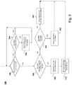
- the module row 8 comprises a controller assembly 12, a plurality of I/O assemblies 14 and end modules 16, 18 connected to each other and mounted to a top hat DIN rail 20, which may extend horizontally or vertically.
- the node may include one or more additional module rows, each comprising more I/O assemblies 14 and first and second end modules 16, 18. Each additional module row may be mounted to a separate DIN rail 20.
- the node may be used to control all or a portion of an industrial process, such as a power generation process. Further, the node may be connected to other nodes of the industrial control system 10, as described more fully below.
- the module row 8 and other module rows of the control system 10 may be mounted in an enclosure such as a cabinet.
- the controller assembly 12 communicates with the I/O assemblies 14 over one or more module buses 22.
- a pair of redundant module buses 22a,b are utilized to increase the integrity of the control system 10. Communication among the modules takes place over both of the module buses 22a,b. However, the modules only use data from the primary bus 22a if it is operating properly. If the primary module bus 22a fails, the modules then use the data from the secondary module bus 22b.
- Each module bus 22 includes a clock line 24 and a data line 26. The data line 26 carries data between the controller assembly 12 and the I/O assemblies 14, while the clock line 24 provides synchronization between the controller assembly 12 and the I/O assemblies 14.
- the message structure and communication protocol utilized by the controller assembly 12 and the I/O assemblies 14 to communicate over the module buses 22a,b include one or more features for ensuring data integrity, such as a cyclical redundancy check (CRC) feature and/or a checksum feature.
- CRC cyclical redundancy check
- each message sent over the module buses 22a,b may contain a CRC code, which is based on the remainder of a polynomial division of the message's data block.
- the receiving device either compares the CRC code of the message with one freshly calculated from the data block, or equivalently, performs a CRC on the whole message and compares the resulting check value with an expected residue constant. If the check values do not match, then the message is determined to contain an error.
- Each I/O assembly 14 handles a plurality of inputs and/or a plurality of outputs.
- a typical control system has a plurality of I/O assemblies 14 handling inputs and/or outputs.
- the inputs may be analog inputs, digital inputs, thermocouple inputs or RTD inputs.
- the outputs may be analog outputs or digital outputs.
- the inputs and outputs (I/O) are typically powered by the sensors and control elements in the field. However, digital outputs may be powered by the I/O assembly 14, such as when the digital outputs are used to energize relay coils.
- Each I/O assembly 14 comprises an I/O module 30 releasably mounted to an I/O base 32.
- Each I/O module 30 includes an outer housing enclosing one or more circuit boards.
- the circuit board(s) of each I/O module 30 includes a microprocessor 34 with memory and a plurality of communication circuits 36 for communicating over the module buses 22a,b. Conditioning circuitry on the circuit board(s) processes field inputs received from sensors in the field or control outputs received from the controller assembly 12, depending on whether the I/O module 30 handles inputs and/or outputs.
- the conditioning circuitry converts between field signals (e.g., analog 4-20 mA, digital 24VDC etc.) and digital bus signals, such as by using analog-to-digital and/or digital-to-analog converters.
- the conditioning circuitry also conditions the signals received from or going to the field, such as by using switches, filters and multiplexers, and isolates the field signals from the controller assembly 12.
- the controller assembly 12 includes a pair of redundant controller modules 50 releasably mounted to a controller base 52.
- Each of the controller modules 50 has a construction similar to each I/O module 30 and includes one or more circuit boards mounted inside an outer housing.
- the circuit board(s) in each controller module 50 includes a microprocessor 33 with memory and a plurality of the communication circuits 36 for communicating over the module buses 22a,b.
- the memory stores control programs that may be executed by the microprocessor 33 of each controller module 50.
- the control programs in each controller module 50 include one or more control loops, such as PID loops, which work on one or more field inputs to generate control outputs.
- the field inputs and control outputs are routed to and from the controller assembly 12 through the I/O assemblies 14 via the module buses 22a,b.
- Each controller module 50 is programmed with and can execute the same control programs; however, only one of the controller modules 50 (the primary) executes the control programs to control the industrial process at any one time. If the primary controller module 50 fails, the other controller module 50 (the secondary) automatically takes over and executes the control programs to control the industrial process.
- the controller base 52 has a plurality of Ethernet jacks 54 that are adapted to receive plugs of Ethernet cables 55, respectively.
- the Ethernet jacks 54 are connected to Ethernet foreign device interfaces 56 in the controller modules 50.
- the controller modules 50 can communicate with other devices over Ethernet cables 55 plugged into the Ethernet jacks. More specifically, the controller modules 50 can communicate with other controller modules 50 (in other nodes) similarly connected to the Ethernet cables 55, and/or with an operator workstation 58 connected to the Ethernet cables 55.
- the controllers 50 may use a protocol, such as Modbus TCP, to communicate with other devices connected to the Ethernet cables.
- the operator workstation 58 may have a graphical user interface (GUI) that displays information from the controller modules 50.
- GUI graphical user interface
- each I/O module 30 and each controller module 50 includes a plurality of communication circuits 36 for communicating over the module buses 22a,b. More specifically, each I/O module 30 and each controller module 50 has four communication circuits 36, two for each module bus 22, with one being used for the clock line 24 and the other being used for the data line 26 of the module bus 22. Each communication circuit 36 is substantially the same. Thus, for purposes of brevity, only one communication circuit 36 will be shown and described, it being understood that the schematic representation and description apply to the other communication circuits 36 as well.
- a communication circuit 36 which generally includes a transceiver 42, a power sense circuit 44 and a ground sense circuit 46.
- the transceiver 42 is connected between the microprocessor 33 or 34 and the module bus 22 and generally includes a driver 60 and a receiver 62.
- the driver 60 transmits signals from microprocessor 33 or 34 to the module bus 22, while the receiver 62 transmits signals from the module bus 22 to the microprocessor 33 or 34.
- the power sense circuit 44 is connected to the high side (VCC) of the driver 60, while the ground sense circuit 46 is connected to the low side (GND) of the driver 60.
- the power sense circuit 44 is operable to sense the current of the high side of the driver 60, which is connected to a power source 64, such a 3 Volt DC power supply.
- the power sense circuit 44 may simply comprise a single resistor.
- the power sense circuit 44 may comprise a differential amplifier connected across a main resistor 68.
- the differential amplifier includes an operational amplifier 70 and resistors 70, 72, 74, 76.
- An output of the differential amplifier is connected to a gain resistor 78.
- the differential amplifier 66 and the gain resistor 78 operate to increase the voltage differential across the main resistor 68 to provide a larger range of acceptable operating values. In this manner, an error value (outside the range) is more distinguishable, thereby reducing the number of false error indications.
- the output from the power sense circuit 44 is an analog signal representative of the current of the high side of the driver 60.
- This analog signal is fed to an analog-to-digital converter (ADC) 80 that converts the analog signal to a digital signal, which is then fed to the microprocessor 33 or 34.
- ADC analog-to-digital converter
- the ground sense circuit 46 is operable to sense the current of the low side of the driver 60.
- the ground sense circuit 46 may simply comprise a single resistor.
- the ground sense circuit 46 may comprise a single-ended amplifier connected between gain resistors 84, 86.
- the single-ended amplifier comprises an operational amplifier 82 with a negative feedback circuit having resistors 90, 92.
- the single-ended amplifier 82 and gain resistors 84, 86 operate to increase the voltage differential between the low side of the driver 60 and ground to provide a larger range of acceptable operating values. In this manner, an error value (outside the range) is more distinguishable, thereby reducing the number of false error indications.
- the output from the ground sense circuit 46 is an analog signal representative of the current of the low side of the driver 60. This analog signal is fed to the analog-to-digital converter (ADC) 80 that converts the analog signal to a digital signal, which is then fed to the microprocessor 33 or 34.
- ADC analog-to-digital converter
- the microprocessor 33 in each controller module 50 receives from each of the communications circuits 36 in the controller module 50 the high side current signal generated by the power sense circuit 44 and the low side current signal generated by the ground sense circuit 46.
- the microprocessor 34 in each I/O module 30 receives from each of the communications circuits 36 in the I/O module 30 the high side current signal generated by the power sense circuit 44 and the low side current signal generated by the ground sense circuit 46.
- each microprocessor 33, 34 receives more than eight current signals.
- the eight current signals are used by a module error detection program 100 in each I/O module 30 to determine whether one of the drivers 60 of the I/O module 30 has failed (e.g., shorted).
- the error detection program 100 is stored in memory and executed by the microprocessor 34.
- the module error detection program 100 initially determines in steps 102, 104, 106, 108 whether a communication error has occurred on the clock lines 24 and/or the data lines 26 of the module buses 22a,b. This determination may be made using a CRC function or other data integrity function.
- step 110 the program 100 waits until the driver(s) 60 for the faulted line(s) send a message to the faulted line(s).
- the program 100 moves to step 120, 122, 124 and/or 126, as the case may be, where the program 100 determines whether the affected driver 60 has a high side current outside of a high range (such as from about 8 mA to about 14 mA) or a low side current outside of a low range (such as from about 2 mA to about 4 mA).
- a high side current outside of a high range such as from about 8 mA to about 14 mA
- a low side current outside of a low range such as from about 2 mA to about 4 mA.
- the determination of the high side and low side currents should be made contemporaneously with the transmission of a message by the driver 60.
- the program 100 determines whether any of the drivers 60 has a high side current or a low side current that is out of range. If one or more of the drivers 60 has a current out of range, the program 100 energizes a red LED 110 on the I/O module 30 in step 132 to provide a visual indication of the error. In addition, the program 100 in step 134 transmits an error message to the primary controller module 50a over the module bus 22a,b that does not have the communication error.
- the error message includes the address of the I/O module 30 and informs the primary controller module 50a that a communication error was detected and that one of the drivers 60 has been determined to have failed.
- the error message may also identify the line (clock or data), whose driver 60 has failed. If in step 130, the program 100 determines that none of the drivers 60 has a high side current or a low side current that is out of range, the error detection program 100 in step 136 transmits a status message to the primary controller module 50a over the module bus 22a,b that does not have the communication error.
- the status message includes the address of the I/O module 30 and informs the primary controller module 50a that a communication error was detected, but none of the drivers 60 in the I/O module 30 have been determined to have failed.
- Each controller module 50 also has a module error detection program stored in memory. However, only the primary controller module 50a executes the program (with its microprocessor 33) to determine whether one of its drivers 60 has failed.
- the module error detection program in each controller module 50 is the same as the error detection program 100 utilized in the I/O modules 30, except it does not include steps 134 and 136.
- each controller module 50 also has a system error detection program 150 stored in memory. However, only the primary controller module 50a executes the system error detection program 150 (with its microprocessor 33). Referring now to Fig. 5 , the system error detection program 150 initially determines in step 152 whether a communication error has occurred on the clock lines 24 and/or the data lines 26 of the module buses 22a,b. If no communication error has occurred, the program 150 proceeds to step 154 to determine whether any status messages from the I/O modules 30 have been received.
- the program 150 determines that a receiver 62 in the I/O module 30 may have failed (e.g. shorted).
- the primary controller module 50a sends a notification of this error (and identifying the affected I/O module 30) to the operator workstation 58, where it may be displayed on the GUI.
- step 152 the program 150 determines that a communication error on a particular bus 22a,b has occurred, the program 150 proceeds to step 158 to determine whether it has received an error message from one of the I/O modules 30 or if the module detection program of the primary controller module 50a has determined that one of its drivers 60 has failed. If no error message has been received and the module detection program of the primary controller module 50a has determined that none of its drivers 60 have failed, then the program 150 proceeds to step 160, where the program 150 determines whether any status messages have been received. If one or more status messages have been received, the program 150 determines that the particular bus 22a,b itself may have failed and sends a notification of this error in step 162 to the operator workstation 58, where it may be displayed on the GUI.
- step 160 determines that one of the receivers 62 of the primary controller module 50a may have failed.
- step 164 the primary controller module 50a sends a notification of this error to the operator workstation 58, where it may be displayed on the GUI.
- step 158 the program 150 determines it has received one or more error messages from the I/O modules 30 or the controller's own module detection program has determined that one or more of its drivers 60 have failed, then the program 150 proceeds to step 168, where the program 150 determines the module(s) having a failed driver 60.
- step170 the primary controller module 50a sends an error message identifying the module(s) having a failed driver 60 to the operator workstation 58, where it may be displayed on the GUI.
- each receiver 62 in the controller modules 50 and the I/O modules 30 may be provided with a power sense circuit 44 and a ground sense circuit 46 for detecting current on the high and lows sides of the receiver 62, respectively.
- a typical control system provided in accordance with this disclosure does not include sense circuits for the receivers in its modules.
Landscapes
- Engineering & Computer Science (AREA)
- Theoretical Computer Science (AREA)
- Physics & Mathematics (AREA)
- General Physics & Mathematics (AREA)
- General Engineering & Computer Science (AREA)
- Quality & Reliability (AREA)
- Automation & Control Theory (AREA)
- Power Engineering (AREA)
- Programmable Controllers (AREA)
- Debugging And Monitoring (AREA)
- Small-Scale Networks (AREA)
Description
- The present disclosure relates to industrial control systems and more particularly to industrial control systems having a controller and input/output modules that communicate over a module bus.
- Industrial control systems, such as distributed control systems, often include one or more controllers that utilize input signals from field devices, such as flow meters, to provide control output signals to final control elements, such as valves, in order to control a process or one or more sub-processes. Known solutions are disclosed in the patent application n°
WO2014/155697A1 - Mitsubishi Electric Corp. [JP]- that discloses a PLC system, and in the USA patent application n°US2008/0211660A1 of Takeuchi that discloses a field device system and filed device system diagnosing method. Such control systems are typically module-based and include one or more controller modules and a plurality of input/output (I/O) modules through which the controller module receives and sends input and output signals from and to the field, respectively. The I/O modules communicate with the controller module(s) over one or more module buses. In conventional control systems, when there is a communication failure on the module bus, it is typically not known whether the communication failure was caused by a failure of the module bus or one of the modules. Detecting the source of the communication failure requires extensive testing. - The present disclosure is directed to a control system having error detection.
- In one aspect of the present disclosure, a process control system includes a module bus and a controller module connected to communicate over the module bus. The controller module is programmed to perform operations for controlling the process using data transmitted over the module bus. The control system further includes a plurality of I/O modules connected to communicate with the controller module over the module bus. Each I/O module includes a microprocessor with memory and a driver for sending information to the module bus. The driver has a high side connected to a voltage source and a low side connected to ground. A sense circuit detects current on the high side of the driver. The microprocessor is operable to execute computer-executable instructions stored in the memory to perform an I/O module error detection method that determines whether the current on the high side of the driver measured by the sense circuit is outside a predetermined high range and, if so, determines that the driver has failed.
- In another aspect of the disclosure, a process control system includes a controller module connected to communicate over first and second module buses. The controller module is programmed to perform operations for controlling the process using data transmitted over the module bus. The control system further includes a plurality of I/O modules connected to communicate with the controller module over the first and second module buses. The controller module and each of the I/O modules include a microprocessor with memory and a driver for sending information to the first module bus. The driver has a high side connected to a voltage source and a low side connected to ground. A power sense circuit detects current on the high side of the driver and a ground sense circuit for detecting current on the low side of the driver. The microprocessor is operable to execute computer-executable instructions stored in the memory to perform a module error detection method that includes determining whether a communication error has occurred on the first module bus. If a communication error has occurred on the first module bus, a determination is made whether the current on the high side of the driver measured by the power sense circuit is outside a predetermined high range and whether the current on the low side of the driver measured by the ground sense circuit is outside a predetermined low range. If either the current on the high side of the driver is determined to be outside the predetermined high range or the current on the low side of the driver is determined to be outside the predetermined low range, a determination is made that the driver has failed.
- In still another aspect of the disclosure, there is a method of detecting errors in a process control system having a plurality of modules connected to communicate over first and second module buses. Each module has a driver for sending information to the first module bus. The driver has a high side connected to a voltage source and a low side connected to ground. In accordance with the method, a determination is made in each of the modules whether a communication error has occurred on the first module bus. The current is measured on the high side of the driver in each of the modules where a communication error has been determined to have occurred. The current is also measured on the low side of the driver in each of the modules where a communication error has been determined to have occurred. The measured current on the high side of the driver in each of the modules where a high side measurement has been made is compared to a predetermined high range, and the measured current on the low side of the driver in each of the modules where a low side measurement has been made is compared to a predetermined low range. The driver in one of the modules is determined to have failed if either the current on the high side of the driver is outside the predetermined high range or the current on the low side of the driver is outside the predetermined low range.
- The features, aspects, and advantages of the present disclosure will become better understood with regard to the following description, appended claims, and accompanying drawings where:
-
Fig. 1 shows a front view of a module row of a control system; -
Fig. 2 shows a schematic of the communication connections of the control system; -
Fig. 3 shows a communication circuit within the modules; -
Fig. 4 shows a flow chart of a module error detection program of the modules; and -
Fig. 5 shows a flow chart of a system error detection program of the control system. - It should be noted that in the detailed description that follows, identical components have the same reference numerals, regardless of whether they are shown in different embodiments of the present disclosure. It should also be noted that in order to be more clear and concise, the drawings may not necessarily be to scale and certain features of an embodiment may be shown in somewhat schematic form.
- Referring now to
FIG. 1 , there is shown a schematic view of amodule row 8 of a node of anindustrial control system 10. Themodule row 8 comprises acontroller assembly 12, a plurality of I/O assemblies 14 andend modules hat DIN rail 20, which may extend horizontally or vertically. The node may include one or more additional module rows, each comprising more I/O assemblies 14 and first andsecond end modules separate DIN rail 20. The node may be used to control all or a portion of an industrial process, such as a power generation process. Further, the node may be connected to other nodes of theindustrial control system 10, as described more fully below. Themodule row 8 and other module rows of thecontrol system 10 may be mounted in an enclosure such as a cabinet. - The
controller assembly 12 communicates with the I/O assemblies 14 over one or more module buses 22. Typically, a pair ofredundant module buses 22a,b are utilized to increase the integrity of thecontrol system 10. Communication among the modules takes place over both of themodule buses 22a,b. However, the modules only use data from theprimary bus 22a if it is operating properly. If theprimary module bus 22a fails, the modules then use the data from thesecondary module bus 22b. Each module bus 22 includes aclock line 24 and adata line 26. Thedata line 26 carries data between thecontroller assembly 12 and the I/O assemblies 14, while theclock line 24 provides synchronization between thecontroller assembly 12 and the I/O assemblies 14. The message structure and communication protocol utilized by thecontroller assembly 12 and the I/O assemblies 14 to communicate over themodule buses 22a,b include one or more features for ensuring data integrity, such as a cyclical redundancy check (CRC) feature and/or a checksum feature. For example each message sent over themodule buses 22a,b may contain a CRC code, which is based on the remainder of a polynomial division of the message's data block. When the message is received, the receiving device either compares the CRC code of the message with one freshly calculated from the data block, or equivalently, performs a CRC on the whole message and compares the resulting check value with an expected residue constant. If the check values do not match, then the message is determined to contain an error. - Each I/
O assembly 14 handles a plurality of inputs and/or a plurality of outputs. A typical control system has a plurality of I/O assemblies 14 handling inputs and/or outputs. The inputs may be analog inputs, digital inputs, thermocouple inputs or RTD inputs. The outputs may be analog outputs or digital outputs. The inputs and outputs (I/O) are typically powered by the sensors and control elements in the field. However, digital outputs may be powered by the I/O assembly 14, such as when the digital outputs are used to energize relay coils. - Each I/
O assembly 14 comprises an I/O module 30 releasably mounted to an I/O base 32. Each I/O module 30 includes an outer housing enclosing one or more circuit boards. The circuit board(s) of each I/O module 30 includes amicroprocessor 34 with memory and a plurality ofcommunication circuits 36 for communicating over themodule buses 22a,b. Conditioning circuitry on the circuit board(s) processes field inputs received from sensors in the field or control outputs received from thecontroller assembly 12, depending on whether the I/O module 30 handles inputs and/or outputs. More specifically, the conditioning circuitry converts between field signals (e.g., analog 4-20 mA, digital 24VDC etc.) and digital bus signals, such as by using analog-to-digital and/or digital-to-analog converters. The conditioning circuitry also conditions the signals received from or going to the field, such as by using switches, filters and multiplexers, and isolates the field signals from thecontroller assembly 12. - The
controller assembly 12 includes a pair ofredundant controller modules 50 releasably mounted to acontroller base 52. Each of thecontroller modules 50 has a construction similar to each I/O module 30 and includes one or more circuit boards mounted inside an outer housing. The circuit board(s) in eachcontroller module 50 includes amicroprocessor 33 with memory and a plurality of thecommunication circuits 36 for communicating over themodule buses 22a,b. The memory stores control programs that may be executed by themicroprocessor 33 of eachcontroller module 50. The control programs in eachcontroller module 50 include one or more control loops, such as PID loops, which work on one or more field inputs to generate control outputs. The field inputs and control outputs are routed to and from thecontroller assembly 12 through the I/O assemblies 14 via themodule buses 22a,b. Eachcontroller module 50 is programmed with and can execute the same control programs; however, only one of the controller modules 50 (the primary) executes the control programs to control the industrial process at any one time. If theprimary controller module 50 fails, the other controller module 50 (the secondary) automatically takes over and executes the control programs to control the industrial process. - The
controller base 52 has a plurality of Ethernet jacks 54 that are adapted to receive plugs ofEthernet cables 55, respectively. The Ethernet jacks 54 are connected to Ethernet foreign device interfaces 56 in thecontroller modules 50. In this manner, thecontroller modules 50 can communicate with other devices overEthernet cables 55 plugged into the Ethernet jacks. More specifically, thecontroller modules 50 can communicate with other controller modules 50 (in other nodes) similarly connected to theEthernet cables 55, and/or with anoperator workstation 58 connected to theEthernet cables 55. Thecontrollers 50 may use a protocol, such as Modbus TCP, to communicate with other devices connected to the Ethernet cables. Theoperator workstation 58 may have a graphical user interface (GUI) that displays information from thecontroller modules 50. - As described above, each I/
O module 30 and eachcontroller module 50 includes a plurality ofcommunication circuits 36 for communicating over themodule buses 22a,b. More specifically, each I/O module 30 and eachcontroller module 50 has fourcommunication circuits 36, two for each module bus 22, with one being used for theclock line 24 and the other being used for thedata line 26 of the module bus 22. Eachcommunication circuit 36 is substantially the same. Thus, for purposes of brevity, only onecommunication circuit 36 will be shown and described, it being understood that the schematic representation and description apply to theother communication circuits 36 as well. - Referring now to
Fig.3 , there is shown acommunication circuit 36, which generally includes atransceiver 42, apower sense circuit 44 and aground sense circuit 46. Thetransceiver 42 is connected between themicroprocessor driver 60 and areceiver 62. Thedriver 60 transmits signals frommicroprocessor receiver 62 transmits signals from the module bus 22 to themicroprocessor power sense circuit 44 is connected to the high side (VCC) of thedriver 60, while theground sense circuit 46 is connected to the low side (GND) of thedriver 60. - The
power sense circuit 44 is operable to sense the current of the high side of thedriver 60, which is connected to apower source 64, such a 3 Volt DC power supply. Thepower sense circuit 44 may simply comprise a single resistor. Alternately, thepower sense circuit 44 may comprise a differential amplifier connected across amain resistor 68. The differential amplifier includes anoperational amplifier 70 andresistors gain resistor 78. The differential amplifier 66 and thegain resistor 78 operate to increase the voltage differential across themain resistor 68 to provide a larger range of acceptable operating values. In this manner, an error value (outside the range) is more distinguishable, thereby reducing the number of false error indications. The output from thepower sense circuit 44 is an analog signal representative of the current of the high side of thedriver 60. This analog signal is fed to an analog-to-digital converter (ADC) 80 that converts the analog signal to a digital signal, which is then fed to themicroprocessor - The
ground sense circuit 46 is operable to sense the current of the low side of thedriver 60. Theground sense circuit 46 may simply comprise a single resistor. Alternately, theground sense circuit 46 may comprise a single-ended amplifier connected betweengain resistors operational amplifier 82 with a negative feedbackcircuit having resistors amplifier 82 and gainresistors driver 60 and ground to provide a larger range of acceptable operating values. In this manner, an error value (outside the range) is more distinguishable, thereby reducing the number of false error indications. The output from theground sense circuit 46 is an analog signal representative of the current of the low side of thedriver 60. This analog signal is fed to the analog-to-digital converter (ADC) 80 that converts the analog signal to a digital signal, which is then fed to themicroprocessor - The
microprocessor 33 in eachcontroller module 50 receives from each of thecommunications circuits 36 in thecontroller module 50 the high side current signal generated by thepower sense circuit 44 and the low side current signal generated by theground sense circuit 46. Similarly, themicroprocessor 34 in each I/O module 30 receives from each of thecommunications circuits 36 in the I/O module 30 the high side current signal generated by thepower sense circuit 44 and the low side current signal generated by theground sense circuit 46. Thus, eachmicroprocessor - The eight current signals are used by a module
error detection program 100 in each I/O module 30 to determine whether one of thedrivers 60 of the I/O module 30 has failed (e.g., shorted). In each I/O module 30, theerror detection program 100 is stored in memory and executed by themicroprocessor 34. With reference now toFig. 4 , the moduleerror detection program 100 initially determines insteps module buses 22a,b. This determination may be made using a CRC function or other data integrity function. If a communication error has occurred, theprogram 100 proceeds to step 110, 112, 114 and/or 116, as the case may be, where theprogram 100 waits until the driver(s) 60 for the faulted line(s) send a message to the faulted line(s). As soon as anaffected driver 60 sends a message, theprogram 100 moves to step 120, 122, 124 and/or 126, as the case may be, where theprogram 100 determines whether the affecteddriver 60 has a high side current outside of a high range (such as from about 8 mA to about 14 mA) or a low side current outside of a low range (such as from about 2 mA to about 4 mA). In this regard, it should be noted that the determination of the high side and low side currents should be made contemporaneously with the transmission of a message by thedriver 60. - If the affected
driver 60 has a high side current outside the high range (such as 7mA or 15mA) or a low side current outside the low range (such as 1 ma or 5mA), it is determined that the affecteddriver 60 has failed . In step 130, theprogram 100 determines whether any of thedrivers 60 has a high side current or a low side current that is out of range. If one or more of thedrivers 60 has a current out of range, theprogram 100 energizes ared LED 110 on the I/O module 30 instep 132 to provide a visual indication of the error. In addition, theprogram 100 instep 134 transmits an error message to the primary controller module 50a over themodule bus 22a,b that does not have the communication error. The error message includes the address of the I/O module 30 and informs the primary controller module 50a that a communication error was detected and that one of thedrivers 60 has been determined to have failed. The error message may also identify the line (clock or data), whosedriver 60 has failed. If in step 130, theprogram 100 determines that none of thedrivers 60 has a high side current or a low side current that is out of range, theerror detection program 100 instep 136 transmits a status message to the primary controller module 50a over themodule bus 22a,b that does not have the communication error. The status message includes the address of the I/O module 30 and informs the primary controller module 50a that a communication error was detected, but none of thedrivers 60 in the I/O module 30 have been determined to have failed. - Each
controller module 50 also has a module error detection program stored in memory. However, only the primary controller module 50a executes the program (with its microprocessor 33) to determine whether one of itsdrivers 60 has failed. The module error detection program in eachcontroller module 50 is the same as theerror detection program 100 utilized in the I/O modules 30, except it does not includesteps - In addition to its module error detection program, each
controller module 50 also has a systemerror detection program 150 stored in memory. However, only the primary controller module 50a executes the system error detection program 150 (with its microprocessor 33). Referring now toFig. 5 , the systemerror detection program 150 initially determines instep 152 whether a communication error has occurred on the clock lines 24 and/or the data lines 26 of themodule buses 22a,b. If no communication error has occurred, theprogram 150 proceeds to step 154 to determine whether any status messages from the I/O modules 30 have been received. If a status message has been received from an I/O module 30 (indicating that the I/O module 30 has detected a communication error, but that nodrivers 60 have been determined to have failed), then theprogram 150 determines that areceiver 62 in the I/O module 30 may have failed (e.g. shorted). Instep 156, the primary controller module 50a sends a notification of this error (and identifying the affected I/O module 30) to theoperator workstation 58, where it may be displayed on the GUI. - If in
step 152, theprogram 150 determines that a communication error on aparticular bus 22a,b has occurred, theprogram 150 proceeds to step 158 to determine whether it has received an error message from one of the I/O modules 30 or if the module detection program of the primary controller module 50a has determined that one of itsdrivers 60 has failed. If no error message has been received and the module detection program of the primary controller module 50a has determined that none of itsdrivers 60 have failed, then theprogram 150 proceeds to step 160, where theprogram 150 determines whether any status messages have been received. If one or more status messages have been received, theprogram 150 determines that theparticular bus 22a,b itself may have failed and sends a notification of this error instep 162 to theoperator workstation 58, where it may be displayed on the GUI. If, instep 160, no status messages have been received, theprogram 150 determines that one of thereceivers 62 of the primary controller module 50a may have failed. Instep 164, the primary controller module 50a sends a notification of this error to theoperator workstation 58, where it may be displayed on the GUI. - If in
step 158, theprogram 150 determines it has received one or more error messages from the I/O modules 30 or the controller's own module detection program has determined that one or more of itsdrivers 60 have failed, then theprogram 150 proceeds to step 168, where theprogram 150 determines the module(s) having a faileddriver 60. In step170, the primary controller module 50a sends an error message identifying the module(s) having a faileddriver 60 to theoperator workstation 58, where it may be displayed on the GUI. - It is to be understood that the description of the foregoing exemplary embodiment(s) is (are) intended to be only illustrative, rather than exhaustive, of the present disclosure. Those of ordinary skill will be able to make certain additions, deletions, and/or modifications to the embodiment(s) of the disclosed subject matter. For example, each
receiver 62 in thecontroller modules 50 and the I/O modules 30 may be provided with apower sense circuit 44 and aground sense circuit 46 for detecting current on the high and lows sides of thereceiver 62, respectively. However, it has been determined that doing so is typically not needed because most communication errors are caused by a failure of a driver. Thus, a typical control system provided in accordance with this disclosure does not include sense circuits for the receivers in its modules.
Claims (16)
- A control system (10) for controlling a process, the control system (10) comprising:a module bus (22, 22a, 22b) over which information may be transmitted;a controller module (50) connected to communicate over the module bus (22, 22a, 22b), the controller module (50) being programmed to perform operations for controlling the process using data transmitted over the module bus (22, 22a, 22b);a plurality of I/O modules (30) connected to communicate with the controller module (50) over the module bus (22, 22a, 22b),each I/O module (30) including:a microprocessor (34) with memory;a driver (60) for sending information to the module bus (22, 22a, 22b), said driver (60) having a high side connected to a voltage source (64) and a low side connected to ground; anda sense circuit (44) for detecting current on the high side of the driver (60);characterized in that the microprocessor (34) is operable to execute computer-executable instructions stored in the memory to perform an I/O module error detection method (100) that comprises determining (102,104,106,108) in each of the I/O modules (30) whether a communication error has occurred on the module bus (22, 22a, 22b) and where the communication error has been determined to have occurred determining (120,122,124,126) whether the current on the high side of the driver (60) measured by the sense circuit (44) is outside of a predetermined high range and, if so, determining (130,132,134) that the driver (60) of the respective module (30) has failed.
- The control system (10) of claim 1, characterized in that the step (102,104,106,108) of determining whether a communication error has occurred on the module bus (22, 22a, 22b) is performed using a cyclical redundancy check function.
- The control system (10) of claim 1, characterized in that the sense circuit (44) is a power sense circuit and wherein each I/O module (30) further includes a ground sense circuit (46) for detecting current on the low side of the driver (60), and wherein the I/O module error detection method (100) further comprises determining (120,122,124,126) whether the current on the low side of the driver (60) measured by the ground sense circuit (46) is outside a predetermined low range and, if so, determining (130,132,134) that the driver (60) has failed.
- The control system (10) of claim 3, characterized in that the I/O module error detection method (100) further comprises determining (102) whether a communication error has occurred on the module bus (22, 22a, 22b) and, if so, then performing the steps of determining (120) whether the current on the high side of the driver (60) measured by the power sense circuit (44) is outside a predetermined high range and whether the current on the low side of the driver (60) measured by the ground sense circuit (46) is outside a predetermined low range.
- The control system (10) of claim 1, characterized in that the module bus (22, 22a, 22b) is a first module bus (22a);
wherein the driver is a first driver (60) for sending information to the first module bus (22a) and the sense circuit (44) is a first sense circuit for detecting current on the high side of the first driver (60);
wherein the control system (10) comprises a second module bus (22b);
wherein the I/O modules (30) each further comprise:a second driver (60) for interfacing with the second module bus (22b), the second driver (60) having a high side connected to the voltage source and a low side connected to ground;a second sense circuit (44) for detecting current on the high side of the second driver (60);wherein the I/O module error detection method (100) further comprises determining (122) whether the current on the high side of the second driver (60) measured by the second sense circuit (44) is outside the predetermined high range and, if so, determining that the second driver (60) has failed. - The control system (10) of claim 5, characterized in that the I/O module error detection method (100) further comprises:sending (134) an error message about the failure of the first driver (60) over the second module bus (22b) to the controller module (50) if the first driver (60) is determined to have failed; andsending (134) an error message about the failure of the second driver (60) over the first module bus (22a) to the controller module (50) if the second driver (60) is determined to have failed.
- The control system (10) of claim 5, characterized in that the first and second sense circuits (44) are first and second power sense circuits and wherein each I/O module (30) further includes first and second ground sense circuits (46) for detecting current on the low side of the first and second drivers (60), respectively, and wherein the I/O module error detection method (100) further comprises:determining (120,122) whether the current on the low side of the first driver (60) measured by the first ground sense circuit (46) is outside the predetermined low range and, if so, determining that the first driver (60) has failed; anddetermining (124,126) whether the current on the low side of the second driver (60) measured by the second ground sense circuit (46) is outside the predetermined low range and, if so, determining that the second driver (60) has failed.
- The control system (10) of claim 7, characterized in that the I/O module error detection method (100) further comprises:determining (102,104) whether a communication error has occurred on the first module bus (22a) and, if so, then performing the steps of determining (120,122) whether the current on the high side of the first driver (60) measured by the first power sense circuit is outside the predetermined high range and whether the current on the low side of the first driver (60) measured by the first ground sense circuit (46) is outside the predetermined low range; anddetermining (106,108) whether a communication error has occurred on the second module bus (22b) and, if so, then performing the steps of determining (124,126) whether the current on the high side of the second driver (60) measured by the second power sense circuit is outside the predetermined high range and whether the current on the low side of the second driver (60) measured by the second ground sense circuit (46) is outside the predetermined low range.
- The control system (10) of claim 8, characterized in that the controller module (50) comprises:a microprocessor (33) with memory;first and second drivers (60) for interfacing with the first and second module buses (22a, 22b) respectively, each of the first and second drivers (60) having a high side connected to a voltage source and a low side connected to ground;a first power sense circuit (44) for detecting current on the high side of the first driver (60);a ground sense circuit (46) for detecting current on the low side of the driver (60); andwherein the microprocessor (33) is operable to execute computer-executable instructions stored in the memory to perform a controller module error detection method (100, 150) that comprises:determining (102, 104,106,108) whether communication errors have occurred on the first and second buses (22a, 22b), respectively;determining (120,122) whether the current on the high side of the first driver (60) measured by the first power sense circuit (44) is outside a predetermined high range if a communication error has occurred on the first bus (22a) ;determining (120,122) whether the current on the low side of the first driver (60) measured by the first ground sense circuit (46) is outside a predetermined low range if a communication error has occurred on the first bus (22a) ;determining (130,132,134) that the first driver (60) has failed if either the current on the high side of the first driver (60) is outside the predetermined high range or the current on the low side of the first driver (60) is outside the predetermined low range;determining (124,126) whether the current on the high side of the second driver (60) measured by the second power sense circuit is outside the predetermined high range if a communication error has occurred on the second bus (22b);determining (124,126) whether the current on the low side of the second driver (60) measured by the second ground sense circuit (46) is outside the predetermined low range if a communication error has occurred on the second bus (22b); anddetermining (130,132,134) that the second driver (60) has failed if either the current on the high side of the second driver (60) is outside the predetermined high range or the current on the low side of the second driver (60) is outside the predetermined low range.
- The control system (10) of claim 1, characterized in that
the module bus (22, 22a, 22b) comprises a first module bus (22a) and a second module bus (22b) over which information may be transmitted, the controller module (50) being connected to communicate over the first and second module buses (22a, 22b) and programmed to perform operations for controlling the process using data transmitted over one or more of the first and second module buses (22a, 22b); and
wherein the plurality of I/O modules (30) are connected to communicate with the controller module (50) over the first and second module buses (22a, 22b);
wherein the controller module (50) comprises:a microprocessor (33) with memory;a driver (60) for sending information to the first module bus (22a) and having a high side connected to a voltage source and a low side connected to ground; anda sense circuit (44) for detecting current on the high side of the driver (60); wherein the sense circuit (44) of each I/O module (30) and the controller module (50) is a power sense circuit;wherein each I/O module (30) and the controller module (50) further comprise a ground sense circuit (46) for detecting current on the low side of the driver (60); and
wherein the microprocessor (33) of the controller module (50) is operable to execute computer-executable instructions stored in the memory to perform a module error detection method (150) that comprises:determining (102,104) whether a communication error has occurred on the first module bus (22a);if a communication error has occurred on the first module bus (22a), determining (120,122) whether the current on the high side of the driver (60) measured by the power sense circuit (44) is outside a predetermined high range and whether the current on the low side of the driver (60) measured by the ground sense circuit (46) is outside a predetermined low range; andif either the current on the high side of the driver (60) is determined to be outside the predetermined high range or the current on the low side of the driver (60) is determined to be outside the predetermined low range, determining (130) that the driver (60) has failed. - The control system (10) of claim 10, characterized in that the module error detection method (100) in the I/O modules (30) further comprises:sending (134) an error message to the controller module (50) over the second module bus (22b) if the driver (60) is determined to have failed; andsending a status message (136) to the controller module (50) over the second module bus (22b) if the driver (60) is determined not to have failed.
- The control system (10) of claim 11, characterized in that further comprises a work station (58) comprising a graphical user interface, and wherein the microprocessor (33) in the controller module (50) executes computer-executable instructions stored in the memory to perform a system error detection method (150) that comprises:determining (152) whether a communication error has occurred on the first module bus (22a);determining (158) whether any error messages have been received and whether the driver (60) of the controller module (50) is determined to have failed if a communication error is determined to have occurred;determining (160) whether any status messages have been received if it is determined that no error messages have been received and the driver (60) of the controller module (50) has not failed;determining (162) that the first module bus (22a) has failed if it is determined that one or more status messages have been received; andsending (170) a message to the work station (58) that the module bus (22a) has been determined to have failed.
- The control system (10) of claim 12, characterized in that the controller module (50) and the I/O modules (30) each further comprise a receiver (60) for receiving information from the first module bus (22a), and wherein the system error detection method (150) further comprises:determining (156) that the receiver (60) of the I/O module (30) has failed if it is determined that a communication error has not occurred and it is determined that a status message has been received from an I/O module (30); andsending (170) a message to the work station that the receiver (60) of the I/O module (30) has been determined to have failed.
- A method of detecting errors in a process control system (10) having a plurality of I/O modules (30) connected to communicate over a module bus (22, 22a, 22b), each I/O module (30) has a driver (60) for sending information to the module bus (22, 22a, 22b) and has a high side connected to a voltage source (64) and a low side connected to ground, the method characterized by comprising:determining (102, 104, 106, 108) in each of the I/O modules (30) whether a communication error has occurred on the module bus (22, 22a, 22b);measuring the current on the high side of the driver (60) in each of the I/O modules (30) where a communication error has been determined to have occurred;comparing (120, 122, 124, 126) the measured current on the high side of the driver (60) in each of the I/O modules (30) where a high side measurement has been made to a predetermined high range;
anddetermining (130) that the driver (60) of the respective I/O module (30) has failed if the current on the high side of the driver (60) is outside the predetermined high range. - The method of claim 14, characterized by further comprising:measuring the current on the low side of the driver (60) in each of the I/O modules (30) where a communication error has been determined to have occurred;comparing (120, 122, 124, 126) the measured current on the low side of the driver (60) in each of the I/O modules (30) where a low side measurement has been made to a predetermined low range;determining (130) that the driver (60) of the respective module (30) has failed if either the current on the high side of the driver (60) is outside the predetermined high range or the current on the low side of the driver (60) is outside the predetermined low range.
- The method of claim 15, characterized by further comprising:in each of the I/O modules (30), after a communication error is determined to have occurred, determining (110, 112, 114, 116) when a message is sent by the driver (60); andwherein in each of the I/O modules (30) where a communication error has been determined to have occurred, the steps of measuring the currents on the high and low sides of the driver (60) are performed when a message is determined to have been sent by the driver (60); orfurther comprising determining that the module bus (22, 22a, 22b) has failed if more than one of the I/O modules (30) detects a communication error on the module bus (22, 22a, 22b) and none of the drivers (60) in the I/O modules (30) are determined to have failed.
Applications Claiming Priority (2)
| Application Number | Priority Date | Filing Date | Title |
|---|---|---|---|
| US201562180896P | 2015-06-17 | 2015-06-17 | |
| PCT/US2016/037837 WO2016205490A1 (en) | 2015-06-17 | 2016-06-16 | Control system with error detection |
Publications (3)
| Publication Number | Publication Date |
|---|---|
| EP3311275A1 EP3311275A1 (en) | 2018-04-25 |
| EP3311275A4 EP3311275A4 (en) | 2018-12-26 |
| EP3311275B1 true EP3311275B1 (en) | 2021-01-27 |
Family
ID=57546181
Family Applications (1)
| Application Number | Title | Priority Date | Filing Date |
|---|---|---|---|
| EP16812420.4A Active EP3311275B1 (en) | 2015-06-17 | 2016-06-16 | Control system with error detection |
Country Status (4)
| Country | Link |
|---|---|
| US (1) | US20180110108A1 (en) |
| EP (1) | EP3311275B1 (en) |
| CN (2) | CN109313590A (en) |
| WO (1) | WO2016205490A1 (en) |
Families Citing this family (2)
| Publication number | Priority date | Publication date | Assignee | Title |
|---|---|---|---|---|
| CN113790648B (en) * | 2021-08-30 | 2023-03-24 | 北京桓安芯数技术有限公司 | Communication fault analysis method and device, electronic equipment and storage medium |
| WO2023158664A1 (en) * | 2022-02-16 | 2023-08-24 | Cantaloupe, Inc. | Method and system to generate an event when a serial interface is disconnected |
Family Cites Families (7)
| Publication number | Priority date | Publication date | Assignee | Title |
|---|---|---|---|---|
| US20080086250A1 (en) * | 2006-10-05 | 2008-04-10 | Renesas Technology America, Inc. | Squib driver circuit diagnostic system and method |
| US20080211660A1 (en) * | 2006-11-09 | 2008-09-04 | Yokogawa Electric Corporation | Field device system and field device system diagnosing method |
| US8344659B2 (en) * | 2009-11-06 | 2013-01-01 | Neofocal Systems, Inc. | System and method for lighting power and control system |
| JP5882691B2 (en) * | 2011-11-21 | 2016-03-09 | サンデンホールディングス株式会社 | Fault detection device for inverter system |
| US8892914B2 (en) * | 2011-12-08 | 2014-11-18 | Active-Semi, Inc. | Programmable fault protect for processor controlled high-side and low-side drivers |
| US9018914B2 (en) * | 2012-10-26 | 2015-04-28 | Maxim Integrated Products, Inc. | Low side NMOS protection circuit for battery pack application |
| EP2980663B1 (en) * | 2013-03-29 | 2017-08-23 | Mitsubishi Electric Corporation | Plc system |
-
2016
- 2016-06-16 CN CN201680048646.4A patent/CN109313590A/en active Pending
- 2016-06-16 EP EP16812420.4A patent/EP3311275B1/en active Active
- 2016-06-16 CN CN202310096792.6A patent/CN115840408A/en active Pending
- 2016-06-16 WO PCT/US2016/037837 patent/WO2016205490A1/en unknown
-
2017
- 2017-12-18 US US15/845,442 patent/US20180110108A1/en not_active Abandoned
Non-Patent Citations (1)
| Title |
|---|
| None * |
Also Published As
| Publication number | Publication date |
|---|---|
| US20180110108A1 (en) | 2018-04-19 |
| CN109313590A (en) | 2019-02-05 |
| EP3311275A1 (en) | 2018-04-25 |
| CN115840408A (en) | 2023-03-24 |
| EP3311275A4 (en) | 2018-12-26 |
| WO2016205490A1 (en) | 2016-12-22 |
Similar Documents
| Publication | Publication Date | Title |
|---|---|---|
| US10552283B2 (en) | Methods and apparatus to communicatively couple field devices to a remote terminal unit | |
| US11016463B2 (en) | Control and data-transfer system, gateway module, I/O module, and method for process control | |
| JP2008181561A (en) | Wiring fault detection, diagnosis and reporting for process control system | |
| EP3311275B1 (en) | Control system with error detection | |
| EP2613474A1 (en) | Method and system for control system redundancy | |
| US10579558B1 (en) | Flexible redundant input/output (I/O) schemes for I/O channels | |
| CN204883358U (en) | Detection apparatus for SIMATICS7 -300 inputs output module | |
| CN113557694A (en) | Network management device, management method, management program, and recording medium | |
| KR101570095B1 (en) | P-type and r-type compatible fire control panel with modularized i/o extension architecture, p-type fire control panel system and r-type fire control panel system | |
| JP2008283259A (en) | Distribution control system, and device controller | |
| JP6174768B1 (en) | Digital pressure gauge and control system | |
| US20170219642A1 (en) | Arrangement with a plurality of peripheral units and a sensor | |
| JP5638045B2 (en) | Numerical control system with detachable filter circuit | |
| EP1962452A1 (en) | A method, a system, a bus master module and a test module for testing the termination of a differential serial communication bus | |
| Singh et al. | Dual Redundant Profibus Network Architecture in hot standby fault tolerant control systems | |
| CN105425780A (en) | Bus fault self-diagnosis device | |
| US20240161713A1 (en) | Systems and methods of fault detection for input/output modules of industrial systems | |
| CN111656203A (en) | Measuring module for an on-board electrical system and associated on-board electrical system for a vehicle | |
| US8704693B1 (en) | Signal interface system and method | |
| KR100508590B1 (en) | Device and method for detecting abnormality of link between main board and node of communication system | |
| KR101493188B1 (en) | Method and multiplex control system for calibrating multiplexed analog terminal/voter module | |
| KR100976395B1 (en) | A method and system for active voltage input | |
| CN112240959A (en) | Control method of power supply apparatus | |
| KR20200040067A (en) | LIN communication controller error detection method and LIN communication device using the method | |
| CN114646905A (en) | Connector detection circuit, method, storage medium, electronic device, and vehicle |
Legal Events
| Date | Code | Title | Description |
|---|---|---|---|
| STAA | Information on the status of an ep patent application or granted ep patent |
Free format text: STATUS: THE INTERNATIONAL PUBLICATION HAS BEEN MADE |
|
| PUAI | Public reference made under article 153(3) epc to a published international application that has entered the european phase |
Free format text: ORIGINAL CODE: 0009012 |
|
| STAA | Information on the status of an ep patent application or granted ep patent |
Free format text: STATUS: REQUEST FOR EXAMINATION WAS MADE |
|
| 17P | Request for examination filed |
Effective date: 20180117 |
|
| AK | Designated contracting states |
Kind code of ref document: A1 Designated state(s): AL AT BE BG CH CY CZ DE DK EE ES FI FR GB GR HR HU IE IS IT LI LT LU LV MC MK MT NL NO PL PT RO RS SE SI SK SM TR |
|
| AX | Request for extension of the european patent |
Extension state: BA ME |
|
| DAV | Request for validation of the european patent (deleted) | ||
| DAX | Request for extension of the european patent (deleted) | ||
| RIC1 | Information provided on ipc code assigned before grant |
Ipc: G06F 11/00 20060101AFI20181115BHEP Ipc: G05B 19/042 20060101ALI20181115BHEP |
|
| A4 | Supplementary search report drawn up and despatched |
Effective date: 20181123 |
|
| STAA | Information on the status of an ep patent application or granted ep patent |
Free format text: STATUS: EXAMINATION IS IN PROGRESS |
|
| 17Q | First examination report despatched |
Effective date: 20190717 |
|
| GRAP | Despatch of communication of intention to grant a patent |
Free format text: ORIGINAL CODE: EPIDOSNIGR1 |
|
| STAA | Information on the status of an ep patent application or granted ep patent |
Free format text: STATUS: GRANT OF PATENT IS INTENDED |
|
| INTG | Intention to grant announced |
Effective date: 20200817 |
|
| GRAS | Grant fee paid |
Free format text: ORIGINAL CODE: EPIDOSNIGR3 |
|
| GRAA | (expected) grant |
Free format text: ORIGINAL CODE: 0009210 |
|
| STAA | Information on the status of an ep patent application or granted ep patent |
Free format text: STATUS: THE PATENT HAS BEEN GRANTED |
|
| AK | Designated contracting states |
Kind code of ref document: B1 Designated state(s): AL AT BE BG CH CY CZ DE DK EE ES FI FR GB GR HR HU IE IS IT LI LT LU LV MC MK MT NL NO PL PT RO RS SE SI SK SM TR |
|
| RAP1 | Party data changed (applicant data changed or rights of an application transferred) |
Owner name: ABB SCHWEIZ AG |
|
| REG | Reference to a national code |
Ref country code: GB Ref legal event code: FG4D |
|
| REG | Reference to a national code |
Ref country code: CH Ref legal event code: EP |
|
| REG | Reference to a national code |
Ref country code: AT Ref legal event code: REF Ref document number: 1358978 Country of ref document: AT Kind code of ref document: T Effective date: 20210215 |
|
| REG | Reference to a national code |
Ref country code: IE Ref legal event code: FG4D |
|
| REG | Reference to a national code |
Ref country code: DE Ref legal event code: R096 Ref document number: 602016052146 Country of ref document: DE |
|
| RAP4 | Party data changed (patent owner data changed or rights of a patent transferred) |
Owner name: ABB SCHWEIZ AG |
|
| REG | Reference to a national code |
Ref country code: NL Ref legal event code: MP Effective date: 20210127 |
|
| REG | Reference to a national code |
Ref country code: LT Ref legal event code: MG9D |
|
| REG | Reference to a national code |
Ref country code: AT Ref legal event code: MK05 Ref document number: 1358978 Country of ref document: AT Kind code of ref document: T Effective date: 20210127 |
|
| PG25 | Lapsed in a contracting state [announced via postgrant information from national office to epo] |
Ref country code: LT Free format text: LAPSE BECAUSE OF FAILURE TO SUBMIT A TRANSLATION OF THE DESCRIPTION OR TO PAY THE FEE WITHIN THE PRESCRIBED TIME-LIMIT Effective date: 20210127 Ref country code: BG Free format text: LAPSE BECAUSE OF FAILURE TO SUBMIT A TRANSLATION OF THE DESCRIPTION OR TO PAY THE FEE WITHIN THE PRESCRIBED TIME-LIMIT Effective date: 20210427 Ref country code: HR Free format text: LAPSE BECAUSE OF FAILURE TO SUBMIT A TRANSLATION OF THE DESCRIPTION OR TO PAY THE FEE WITHIN THE PRESCRIBED TIME-LIMIT Effective date: 20210127 Ref country code: GR Free format text: LAPSE BECAUSE OF FAILURE TO SUBMIT A TRANSLATION OF THE DESCRIPTION OR TO PAY THE FEE WITHIN THE PRESCRIBED TIME-LIMIT Effective date: 20210428 Ref country code: FI Free format text: LAPSE BECAUSE OF FAILURE TO SUBMIT A TRANSLATION OF THE DESCRIPTION OR TO PAY THE FEE WITHIN THE PRESCRIBED TIME-LIMIT Effective date: 20210127 Ref country code: NO Free format text: LAPSE BECAUSE OF FAILURE TO SUBMIT A TRANSLATION OF THE DESCRIPTION OR TO PAY THE FEE WITHIN THE PRESCRIBED TIME-LIMIT Effective date: 20210427 Ref country code: PT Free format text: LAPSE BECAUSE OF FAILURE TO SUBMIT A TRANSLATION OF THE DESCRIPTION OR TO PAY THE FEE WITHIN THE PRESCRIBED TIME-LIMIT Effective date: 20210527 |
|
| PG25 | Lapsed in a contracting state [announced via postgrant information from national office to epo] |
Ref country code: SE Free format text: LAPSE BECAUSE OF FAILURE TO SUBMIT A TRANSLATION OF THE DESCRIPTION OR TO PAY THE FEE WITHIN THE PRESCRIBED TIME-LIMIT Effective date: 20210127 Ref country code: AT Free format text: LAPSE BECAUSE OF FAILURE TO SUBMIT A TRANSLATION OF THE DESCRIPTION OR TO PAY THE FEE WITHIN THE PRESCRIBED TIME-LIMIT Effective date: 20210127 Ref country code: LV Free format text: LAPSE BECAUSE OF FAILURE TO SUBMIT A TRANSLATION OF THE DESCRIPTION OR TO PAY THE FEE WITHIN THE PRESCRIBED TIME-LIMIT Effective date: 20210127 Ref country code: PL Free format text: LAPSE BECAUSE OF FAILURE TO SUBMIT A TRANSLATION OF THE DESCRIPTION OR TO PAY THE FEE WITHIN THE PRESCRIBED TIME-LIMIT Effective date: 20210127 Ref country code: RS Free format text: LAPSE BECAUSE OF FAILURE TO SUBMIT A TRANSLATION OF THE DESCRIPTION OR TO PAY THE FEE WITHIN THE PRESCRIBED TIME-LIMIT Effective date: 20210127 |
|
| PG25 | Lapsed in a contracting state [announced via postgrant information from national office to epo] |
Ref country code: IS Free format text: LAPSE BECAUSE OF FAILURE TO SUBMIT A TRANSLATION OF THE DESCRIPTION OR TO PAY THE FEE WITHIN THE PRESCRIBED TIME-LIMIT Effective date: 20210527 |
|
| REG | Reference to a national code |
Ref country code: DE Ref legal event code: R097 Ref document number: 602016052146 Country of ref document: DE |
|
| PG25 | Lapsed in a contracting state [announced via postgrant information from national office to epo] |
Ref country code: SM Free format text: LAPSE BECAUSE OF FAILURE TO SUBMIT A TRANSLATION OF THE DESCRIPTION OR TO PAY THE FEE WITHIN THE PRESCRIBED TIME-LIMIT Effective date: 20210127 Ref country code: CZ Free format text: LAPSE BECAUSE OF FAILURE TO SUBMIT A TRANSLATION OF THE DESCRIPTION OR TO PAY THE FEE WITHIN THE PRESCRIBED TIME-LIMIT Effective date: 20210127 Ref country code: EE Free format text: LAPSE BECAUSE OF FAILURE TO SUBMIT A TRANSLATION OF THE DESCRIPTION OR TO PAY THE FEE WITHIN THE PRESCRIBED TIME-LIMIT Effective date: 20210127 |
|
| PG25 | Lapsed in a contracting state [announced via postgrant information from national office to epo] |
Ref country code: SK Free format text: LAPSE BECAUSE OF FAILURE TO SUBMIT A TRANSLATION OF THE DESCRIPTION OR TO PAY THE FEE WITHIN THE PRESCRIBED TIME-LIMIT Effective date: 20210127 Ref country code: RO Free format text: LAPSE BECAUSE OF FAILURE TO SUBMIT A TRANSLATION OF THE DESCRIPTION OR TO PAY THE FEE WITHIN THE PRESCRIBED TIME-LIMIT Effective date: 20210127 Ref country code: DK Free format text: LAPSE BECAUSE OF FAILURE TO SUBMIT A TRANSLATION OF THE DESCRIPTION OR TO PAY THE FEE WITHIN THE PRESCRIBED TIME-LIMIT Effective date: 20210127 |
|
| PLBE | No opposition filed within time limit |
Free format text: ORIGINAL CODE: 0009261 |
|
| STAA | Information on the status of an ep patent application or granted ep patent |
Free format text: STATUS: NO OPPOSITION FILED WITHIN TIME LIMIT |
|
| 26N | No opposition filed |
Effective date: 20211028 |
|
| PG25 | Lapsed in a contracting state [announced via postgrant information from national office to epo] |
Ref country code: ES Free format text: LAPSE BECAUSE OF FAILURE TO SUBMIT A TRANSLATION OF THE DESCRIPTION OR TO PAY THE FEE WITHIN THE PRESCRIBED TIME-LIMIT Effective date: 20210127 Ref country code: AL Free format text: LAPSE BECAUSE OF FAILURE TO SUBMIT A TRANSLATION OF THE DESCRIPTION OR TO PAY THE FEE WITHIN THE PRESCRIBED TIME-LIMIT Effective date: 20210127 Ref country code: MC Free format text: LAPSE BECAUSE OF FAILURE TO SUBMIT A TRANSLATION OF THE DESCRIPTION OR TO PAY THE FEE WITHIN THE PRESCRIBED TIME-LIMIT Effective date: 20210127 |
|
| REG | Reference to a national code |
Ref country code: CH Ref legal event code: PL |
|
| PG25 | Lapsed in a contracting state [announced via postgrant information from national office to epo] |
Ref country code: SI Free format text: LAPSE BECAUSE OF FAILURE TO SUBMIT A TRANSLATION OF THE DESCRIPTION OR TO PAY THE FEE WITHIN THE PRESCRIBED TIME-LIMIT Effective date: 20210127 |
|
| REG | Reference to a national code |
Ref country code: BE Ref legal event code: MM Effective date: 20210630 |
|
| PG25 | Lapsed in a contracting state [announced via postgrant information from national office to epo] |
Ref country code: LU Free format text: LAPSE BECAUSE OF NON-PAYMENT OF DUE FEES Effective date: 20210616 |
|
| PG25 | Lapsed in a contracting state [announced via postgrant information from national office to epo] |
Ref country code: LI Free format text: LAPSE BECAUSE OF NON-PAYMENT OF DUE FEES Effective date: 20210630 Ref country code: IT Free format text: LAPSE BECAUSE OF FAILURE TO SUBMIT A TRANSLATION OF THE DESCRIPTION OR TO PAY THE FEE WITHIN THE PRESCRIBED TIME-LIMIT Effective date: 20210127 Ref country code: IE Free format text: LAPSE BECAUSE OF NON-PAYMENT OF DUE FEES Effective date: 20210616 Ref country code: CH Free format text: LAPSE BECAUSE OF NON-PAYMENT OF DUE FEES Effective date: 20210630 |
|
| PG25 | Lapsed in a contracting state [announced via postgrant information from national office to epo] |
Ref country code: IS Free format text: LAPSE BECAUSE OF FAILURE TO SUBMIT A TRANSLATION OF THE DESCRIPTION OR TO PAY THE FEE WITHIN THE PRESCRIBED TIME-LIMIT Effective date: 20210527 Ref country code: FR Free format text: LAPSE BECAUSE OF NON-PAYMENT OF DUE FEES Effective date: 20210630 |
|
| PG25 | Lapsed in a contracting state [announced via postgrant information from national office to epo] |
Ref country code: BE Free format text: LAPSE BECAUSE OF NON-PAYMENT OF DUE FEES Effective date: 20210630 |
|
| PG25 | Lapsed in a contracting state [announced via postgrant information from national office to epo] |
Ref country code: NL Free format text: LAPSE BECAUSE OF NON-PAYMENT OF DUE FEES Effective date: 20210127 Ref country code: CY Free format text: LAPSE BECAUSE OF FAILURE TO SUBMIT A TRANSLATION OF THE DESCRIPTION OR TO PAY THE FEE WITHIN THE PRESCRIBED TIME-LIMIT Effective date: 20210127 |
|
| PG25 | Lapsed in a contracting state [announced via postgrant information from national office to epo] |
Ref country code: HU Free format text: LAPSE BECAUSE OF FAILURE TO SUBMIT A TRANSLATION OF THE DESCRIPTION OR TO PAY THE FEE WITHIN THE PRESCRIBED TIME-LIMIT; INVALID AB INITIO Effective date: 20160616 |
|
| PGFP | Annual fee paid to national office [announced via postgrant information from national office to epo] |
Ref country code: DE Payment date: 20230620 Year of fee payment: 8 |
|
| PGFP | Annual fee paid to national office [announced via postgrant information from national office to epo] |
Ref country code: GB Payment date: 20230622 Year of fee payment: 8 |
|
| PG25 | Lapsed in a contracting state [announced via postgrant information from national office to epo] |
Ref country code: MK Free format text: LAPSE BECAUSE OF FAILURE TO SUBMIT A TRANSLATION OF THE DESCRIPTION OR TO PAY THE FEE WITHIN THE PRESCRIBED TIME-LIMIT Effective date: 20210127 |