EP3290931B1 - Interferometric voltage sensor with error compensation - Google Patents
Interferometric voltage sensor with error compensation Download PDFInfo
- Publication number
- EP3290931B1 EP3290931B1 EP16187127.2A EP16187127A EP3290931B1 EP 3290931 B1 EP3290931 B1 EP 3290931B1 EP 16187127 A EP16187127 A EP 16187127A EP 3290931 B1 EP3290931 B1 EP 3290931B1
- Authority
- EP
- European Patent Office
- Prior art keywords
- voltage
- electro
- optic element
- faraday rotator
- calibration
- Prior art date
- Legal status (The legal status is an assumption and is not a legal conclusion. Google has not performed a legal analysis and makes no representation as to the accuracy of the status listed.)
- Not-in-force
Links
- 238000000034 method Methods 0.000 claims description 41
- 230000010363 phase shift Effects 0.000 claims description 36
- 230000010287 polarization Effects 0.000 claims description 33
- 238000005259 measurement Methods 0.000 claims description 25
- 230000005684 electric field Effects 0.000 claims description 13
- 230000001419 dependent effect Effects 0.000 claims description 7
- 230000000630 rising effect Effects 0.000 claims description 3
- 239000013078 crystal Substances 0.000 description 20
- 239000000835 fiber Substances 0.000 description 19
- 230000003287 optical effect Effects 0.000 description 13
- 230000009897 systematic effect Effects 0.000 description 13
- 230000005693 optoelectronics Effects 0.000 description 8
- 238000001228 spectrum Methods 0.000 description 6
- 239000011159 matrix material Substances 0.000 description 5
- 230000008859 change Effects 0.000 description 4
- 238000001514 detection method Methods 0.000 description 3
- 239000007789 gas Substances 0.000 description 3
- 230000003595 spectral effect Effects 0.000 description 3
- IJGRMHOSHXDMSA-UHFFFAOYSA-N Atomic nitrogen Chemical compound N#N IJGRMHOSHXDMSA-UHFFFAOYSA-N 0.000 description 2
- CURLTUGMZLYLDI-UHFFFAOYSA-N Carbon dioxide Chemical compound O=C=O CURLTUGMZLYLDI-UHFFFAOYSA-N 0.000 description 2
- 230000005697 Pockels effect Effects 0.000 description 2
- 230000000737 periodic effect Effects 0.000 description 2
- 230000008569 process Effects 0.000 description 2
- 238000012935 Averaging Methods 0.000 description 1
- QVGXLLKOCUKJST-UHFFFAOYSA-N atomic oxygen Chemical compound [O] QVGXLLKOCUKJST-UHFFFAOYSA-N 0.000 description 1
- 238000009529 body temperature measurement Methods 0.000 description 1
- 229910002092 carbon dioxide Inorganic materials 0.000 description 1
- 239000001569 carbon dioxide Substances 0.000 description 1
- 238000006880 cross-coupling reaction Methods 0.000 description 1
- 230000000694 effects Effects 0.000 description 1
- IYRWEQXVUNLMAY-UHFFFAOYSA-N fluoroketone group Chemical group FC(=O)F IYRWEQXVUNLMAY-UHFFFAOYSA-N 0.000 description 1
- 239000000203 mixture Substances 0.000 description 1
- 229910052757 nitrogen Inorganic materials 0.000 description 1
- 239000001301 oxygen Substances 0.000 description 1
- 229910052760 oxygen Inorganic materials 0.000 description 1
- 230000009467 reduction Effects 0.000 description 1
Images


Classifications
-
- G—PHYSICS
- G01—MEASURING; TESTING
- G01R—MEASURING ELECTRIC VARIABLES; MEASURING MAGNETIC VARIABLES
- G01R15/00—Details of measuring arrangements of the types provided for in groups G01R17/00 - G01R29/00, G01R33/00 - G01R33/26 or G01R35/00
- G01R15/14—Adaptations providing voltage or current isolation, e.g. for high-voltage or high-current networks
- G01R15/24—Adaptations providing voltage or current isolation, e.g. for high-voltage or high-current networks using light-modulating devices
- G01R15/241—Adaptations providing voltage or current isolation, e.g. for high-voltage or high-current networks using light-modulating devices using electro-optical modulators, e.g. electro-absorption
- G01R15/242—Adaptations providing voltage or current isolation, e.g. for high-voltage or high-current networks using light-modulating devices using electro-optical modulators, e.g. electro-absorption based on the Pockels effect, i.e. linear electro-optic effect
-
- G—PHYSICS
- G01—MEASURING; TESTING
- G01R—MEASURING ELECTRIC VARIABLES; MEASURING MAGNETIC VARIABLES
- G01R15/00—Details of measuring arrangements of the types provided for in groups G01R17/00 - G01R29/00, G01R33/00 - G01R33/26 or G01R35/00
- G01R15/14—Adaptations providing voltage or current isolation, e.g. for high-voltage or high-current networks
- G01R15/24—Adaptations providing voltage or current isolation, e.g. for high-voltage or high-current networks using light-modulating devices
- G01R15/245—Adaptations providing voltage or current isolation, e.g. for high-voltage or high-current networks using light-modulating devices using magneto-optical modulators, e.g. based on the Faraday or Cotton-Mouton effect
- G01R15/246—Adaptations providing voltage or current isolation, e.g. for high-voltage or high-current networks using light-modulating devices using magneto-optical modulators, e.g. based on the Faraday or Cotton-Mouton effect based on the Faraday, i.e. linear magneto-optic, effect
-
- G—PHYSICS
- G01—MEASURING; TESTING
- G01R—MEASURING ELECTRIC VARIABLES; MEASURING MAGNETIC VARIABLES
- G01R19/00—Arrangements for measuring currents or voltages or for indicating presence or sign thereof
- G01R19/0084—Arrangements for measuring currents or voltages or for indicating presence or sign thereof measuring voltage only
-
- G—PHYSICS
- G01—MEASURING; TESTING
- G01R—MEASURING ELECTRIC VARIABLES; MEASURING MAGNETIC VARIABLES
- G01R35/00—Testing or calibrating of apparatus covered by the other groups of this subclass
- G01R35/005—Calibrating; Standards or reference devices, e.g. voltage or resistance standards, "golden" references
-
- G—PHYSICS
- G01—MEASURING; TESTING
- G01C—MEASURING DISTANCES, LEVELS OR BEARINGS; SURVEYING; NAVIGATION; GYROSCOPIC INSTRUMENTS; PHOTOGRAMMETRY OR VIDEOGRAMMETRY
- G01C19/00—Gyroscopes; Turn-sensitive devices using vibrating masses; Turn-sensitive devices without moving masses; Measuring angular rate using gyroscopic effects
- G01C19/58—Turn-sensitive devices without moving masses
- G01C19/64—Gyrometers using the Sagnac effect, i.e. rotation-induced shifts between counter-rotating electromagnetic beams
- G01C19/72—Gyrometers using the Sagnac effect, i.e. rotation-induced shifts between counter-rotating electromagnetic beams with counter-rotating light beams in a passive ring, e.g. fibre laser gyrometers
-
- G—PHYSICS
- G01—MEASURING; TESTING
- G01R—MEASURING ELECTRIC VARIABLES; MEASURING MAGNETIC VARIABLES
- G01R15/00—Details of measuring arrangements of the types provided for in groups G01R17/00 - G01R29/00, G01R33/00 - G01R33/26 or G01R35/00
- G01R15/14—Adaptations providing voltage or current isolation, e.g. for high-voltage or high-current networks
- G01R15/24—Adaptations providing voltage or current isolation, e.g. for high-voltage or high-current networks using light-modulating devices
- G01R15/247—Details of the circuitry or construction of devices covered by G01R15/241 - G01R15/246
-
- G—PHYSICS
- G01—MEASURING; TESTING
- G01R—MEASURING ELECTRIC VARIABLES; MEASURING MAGNETIC VARIABLES
- G01R33/00—Arrangements or instruments for measuring magnetic variables
- G01R33/02—Measuring direction or magnitude of magnetic fields or magnetic flux
- G01R33/032—Measuring direction or magnitude of magnetic fields or magnetic flux using magneto-optic devices, e.g. Faraday or Cotton-Mouton effect
- G01R33/0322—Measuring direction or magnitude of magnetic fields or magnetic flux using magneto-optic devices, e.g. Faraday or Cotton-Mouton effect using the Faraday or Voigt effect
-
- G—PHYSICS
- G02—OPTICS
- G02F—OPTICAL DEVICES OR ARRANGEMENTS FOR THE CONTROL OF LIGHT BY MODIFICATION OF THE OPTICAL PROPERTIES OF THE MEDIA OF THE ELEMENTS INVOLVED THEREIN; NON-LINEAR OPTICS; FREQUENCY-CHANGING OF LIGHT; OPTICAL LOGIC ELEMENTS; OPTICAL ANALOGUE/DIGITAL CONVERTERS
- G02F1/00—Devices or arrangements for the control of the intensity, colour, phase, polarisation or direction of light arriving from an independent light source, e.g. switching, gating or modulating; Non-linear optics
- G02F1/01—Devices or arrangements for the control of the intensity, colour, phase, polarisation or direction of light arriving from an independent light source, e.g. switching, gating or modulating; Non-linear optics for the control of the intensity, phase, polarisation or colour
- G02F1/0136—Devices or arrangements for the control of the intensity, colour, phase, polarisation or direction of light arriving from an independent light source, e.g. switching, gating or modulating; Non-linear optics for the control of the intensity, phase, polarisation or colour for the control of polarisation, e.g. state of polarisation [SOP] control, polarisation scrambling, TE-TM mode conversion or separation
Definitions
- This invention pertains to the systematic error compensation scheme used in an optical voltage sensor. It relates to a method and a device for measuring voltages.
- the advantages of the reflective modulation phase detection (MPD) measurement scheme [2] are, in particular, the excellent stability of its scale factor and zero point, both of which are needed for the accurate measurement of a DC voltage.
- MPD reflective modulation phase detection
- the concept uses a 45° Faraday rotator inserted between the polarization-maintaining (PM) fiber and the electro-optic crystal in the voltage sensor.
- An interference-contrast-based period disambiguation method has been developed to enable the extension of the unambiguous voltage measurement range to ⁇ 500 kV [1].
- Modulation phase detection [2] is a powerful interrogation technique to measure phase shift in an optical system.
- MPD sensors can e.g. be implemented in a reciprocal configuration, either in the form of a Sagnac interferometer or in a reflective form, in order to cancel phase shifts from additional birefringent elements in the system (such as PM fibers or the phase modulator crystal), which may drift slowly, e.g. with temperature change or mechanical disturbance.
- the MPD detection scheme can also be used for optical voltage sensing.
- a suitable device is shown in Fig. 1 . It comprises an MPD optoelectronics module 1 for generating waves along both polarization directions of a polarization maintaining (PM) fiber 2.
- a collimator 3 sends these waves through a 45° Faraday rotator 4 and into a first end of Pockels effect crystal 5, which is being exposed to the electrical field from the voltage to be measured.
- the waves are reflected by a reflector 6 and sent back through the components 1 - 5 and into MPD optoelectronics module 1.
- Faraday rotator 4 rotates both linear polarizations from PM fiber 2 by 45° before they propagate along the electro-optic axes of sensing crystal 5 [3].
- the reflected waves pass through Faraday rotator 4 again, further rotating the polarizations by 45° in the same direction, thereby making a combined 90° rotation from the input polarizations, which is equivalent to a swap between the two orthogonal linear polarizations.
- the two returning polarizations are brought to interference in MPD optoelectronics module 1, which gives rise to a signal with a basically periodic dependence of the voltage to be measured.
- the voltage range exceeds the ⁇ -voltage of the sensing crystal (e.g. 75 kV for BGO), it is necessary to resolve the phase shift period ambiguity in order to uniquely determine the applied voltage. This is particularly critical for DC measurements, where history tracking methods such as zero-crossing counting are not applicable.
- the interference contrast of a low-coherence light source can be used to determine the phase shift period [1]. It can be shown that for both an open-loop sinusoidal-modulation and a closed-loop square-wave modulation MPD system, it is possible to measure the interference contrast in addition to the phase shift principal value, and to combine them to determine a unique voltage value.
- Faraday rotator 4 has a perfect 45° rotation angle, and the PM fiber axes are aligned exactly at 45° with respect to the electro-optic axes of sensing crystal 5.
- deviations in the Faraday rotation angle and angular alignment are difficult to avoid, and the Faraday rotation angle is also strongly dependent on wavelength and temperature. These systematic errors can cause the measurement result to deviate significantly from theoretical expectations.
- the problem to be solved is to provide a method and device of this type with a large measurement range that are less sensitive to misalignments and/or variations of the rotation in the Faraday rotator.
- the method comprises the steps of:
- the invention also relates to a device for measuring a voltage.
- the device comprises a Faraday rotator, an electro-optic element, a reflector, a light source positioned to send light through said Faraday rotator and said electro-optic element onto the reflector and from there back through said electro-optic element and said Faraday rotator, wherein two polarizations of said light (namely those polarized along the principal refractive index axes of the electro-optic element) suffer a voltage-dependent phase shift in said electro-optic element, a light detector positioned to measure an interference between said two polarizations returning from that electro-optic element and said Faraday rotator, and a control unit adapted and structured to carry at the steps described above.
- the method can further comprise calibration steps. These calibration steps comprise:
- the contrast and principal value are measured for a plurality of voltage values of the reference voltage. Using the measured values of the contrast and principal value at the several voltage values, one or more of the calibration values can then be calculated.
- the varying electrical field is varied over a range sufficient to generate phase shifts between said polarizations that vary by at least ⁇ , in particular by at least 2 ⁇ .
- the uncompensated complex value K is substantially periodic in the phase shift between the polarizations and describes a spiral in the complex plane.
- the center as well as the real and imaginary axis amplitudes of this spiral basically describe the calibration values.
- the complex argument of K substantially corresponds to the phase shift between the polarization.
- the center and axis amplitudes of the spiral can best be determined by varying the phase shift by at least ⁇ , in particular by at least 2 ⁇ .
- the calibration steps advantageously comprise the step of determining a center and real and imaginary scaling factors of a spiral connecting said uncompensated complex value K when varying said principal value ⁇ .
- the invention is based on the idea that a refined model and scheme are needed to account for and compensate errors caused by misalignment of the components and non-45° rotations in the Faraday rotator.
- the invention is particularly suited to measure high voltages of at least 100 kV, in particular of at least 500 kV. It can advantageously be used for DC voltages. But it can also be used for measuring AC voltages, in which case the rising of falling slope of the voltage can be used to determine the corrected values k ⁇ and ⁇ .
- the technique can provide high accuracy, with errors ⁇ 0.2%.
- the sensor and method are e.g. ideal for various HVDC applications, including HVDC Light, HVDC Classic, and HVDC for offshore DC applications, e.g. in a DC GIS. Accordingly, the invention also relates to the use of the device or method for measuring a DC voltage of at least 100 kV.
- MPD optoelectronics module 1 for generating waves along both polarization directions of a polarization maintaining (PM) fiber 2.
- a collimator 3 sends these waves through a 45° Faraday rotator 4 and into a first end of Pockels effect crystal 5, which is being exposed to the electrical field from the voltage to be measured.
- the waves are reflected by a reflector 6 and sent back through the components 1 - 5 and into MPD optoelectronics module 1.
- Faraday rotator 4 rotates both linear polarizations from PM fiber 2 by 45° before they propagate along the electro-optic axes (principal refractive index axes) of sensing crystal 5 [3].
- the reflected waves pass through Faraday rotator 4 again, further rotating the polarizations by 45° in the same direction, thereby making a combined 90° rotation from the input polarizations, which is equivalent to a swap between the two orthogonal linear polarizations.
- the optoelectronics module 1 comprises a phase modulator 7 adapted to introduce a phase shift ⁇ m between the two light polarizations returning in PM fiber 2 before they are brought to interference in a detector 8.
- the coherence length of light source 9 is advantageously between 5 ⁇ ⁇ 0 and 100 ⁇ ⁇ 0 , with ⁇ 0 being the center wavelength of the light source, in order to obtain a good variation of interference contrast k when changing the phase between the two polarizations by a few multiples of 2 ⁇ .
- the device further comprises a control unit 10 adapted and structured to carry out the measurement and error compensation methods described below. It can e.g. be formed by a microprocessor or microcontroller provided with suitable interface circuits.
- the interference contrast k and principal value ⁇ can e.g. be determined e.g. as described in [1].
- the trace of a complex output with its absolute value equal to the MPD-measured interference contrast k and its argument equal to the MPD-measured phase shift principal value ⁇ is a spiral curve in the complex plane.
- the influence of systematic errors in a reflective optical voltage sensor, such as Faraday rotation angle error and axis alignment error, can be represented as a shift of the spiral center from the complex plane origin, and scaling of the spiral radii along the real and imaginary axes.
- the systematic measurement error can then be compensated by recentering and rescaling the measured spiral trace, yielding a more accurate phase shift measurement.
- the double-pass electro-optic phase shift ⁇ is proportional to the applied voltage V , which we aim to recover from the measurement.
- the component matrices represent a 45° Faraday rotation, a -45° rotation between PM fiber 2 and sensing crystal 4 electro-optic axes, mirror reflection, the phase delay in crystal 4, the axes rotation and Faraday rotation in the mirrored reference frame, respectively.
- the result presented above is valid only for a MPD system operating at a single wavelength.
- a low-coherence light source 9 an ensemble of wavelengths is contained in the broadband spectrum.
- the electro-optic group delay ⁇ is proportional to the electro-optic phase shift ⁇ 0 when the applied voltage varies.
- ⁇ / ⁇ 0 0.76 fs/rad at 1310 nm.
- the detected light power in the MPD system is the ensemble average across the spectrum.
- ⁇ I ⁇ 1 2 1 + Re ⁇ g 2 ⁇ e i ⁇ m
- the MPD-retrieved complex output K ke i ⁇ plotted on the complex plane is a spiral curve emanating from (or converging into) the origin of the complex plane.
- a birefringent element e.g. a birefringent crystal
- the Faraday rotation angle may not be exactly 45°, or the axes of the PM fiber may not be aligned exactly at 45° with the electro-optic axes of the sensing crystal. In such cases, cross-coupling occurs between orthogonal polarizations as the waves enter and exit the sensing crystal, which would disturb the MPD measurement result.
- the values of K 0 (which is complex valued), r 1 and r 2 (both of which are real-valued) are calibration values, which are determined in a calibration process. For example, in this process, one may vary the applied voltage V in a certain range, and record the complex output K ( V ) at the same time.
- the selected voltage range should preferably cover at least one ⁇ -voltage for a reflective voltage sensor, whereby the K ( V ) trace would make at least one full circle around K 0 .
- the selected voltage range should be in a region where the coherence function A ( ⁇ + ⁇ 0 ) is largely linear with the voltage.
- the compensation with parameters determined by the simple method M1 results in significant reduction of the phase shift error over the uncompensated result. Further fine adjustment of the calibrated spiral parameters using a fitting method leads to even lower phase shift errors.
- the complex output K trace may be rotated about the origin, which would make the spiral center appear shifted also along the imaginary axis. This effect has been observed in some measurements.
- the same procedure can be repeated for K ⁇ e -i ⁇ to determine the other spiral parameters r 1 and r 2 . If no rotation compensation is required, the calibration value ⁇ can be set to 0 and no explicit calibration measurement may be required for its determination.
- the above-mentioned calibration should be performed at a few representative temperatures in the given range to determine how these parameters vary with temperature. In real operation, a parallel temperature measurement is needed to properly adjust these parameters for the actual operating condition.
- the present method advantageously comprises the steps of measuring the temperature at Faraday rotator 4 and selecting the calibration values as a function of this temperature.
- the calibration values are advantageously measured for a plurality of temperatures.
- step 1 calibration In an AC voltage measurement, the instantaneous voltage continuously sweeps along a section of the spiral trace. Therefore, it is possible to do the calibration steps (step 1 calibration) in real time during a rising or falling slope of the voltage. If the Faraday rotation angle deviation ⁇ F 0 has the same sign in the entire temperature range, one may use the temperature dependence of the real-time-calibrated spiral parameters (also optionally the temperature dependence of the group delay offset ⁇ 0 ) to determine the temperature, and to perform temperature compensation of other parameters, e.g. of the electro-optic coefficient.
- Electro-optic crystal 5 can be replaced by any other electro-optic element that has exhibits a birefringence depending on the applied electrical field.
- the calibration values r 1 , r 2 , and K 0 and, optionally, ⁇ are device-dependent.
- the techniques shown here allow the compensation of systematic errors for an optical DC voltage sensor with measurement range > ⁇ 500 kV to achieve an accuracy of ⁇ 0.2%.
- GIS DC gas-insulated switching
- Such GIS may be filled with dielectric gas based on SF6 or alternative gases, such as fluoroketones or fluoronitriles, preferably in mixtures with a background gas, such as e.g. selected from: nitrogen, carbon dioxide and oxygen.
Description
- This invention pertains to the systematic error compensation scheme used in an optical voltage sensor. It relates to a method and a device for measuring voltages.
- The advantages of the reflective modulation phase detection (MPD) measurement scheme [2] are, in particular, the excellent stability of its scale factor and zero point, both of which are needed for the accurate measurement of a DC voltage. In order to achieve polarization mode swapping - a key requirement for reflective MPD - the concept uses a 45° Faraday rotator inserted between the polarization-maintaining (PM) fiber and the electro-optic crystal in the voltage sensor. An interference-contrast-based period disambiguation method has been developed to enable the extension of the unambiguous voltage measurement range to ±500 kV [1].
- In a real optical voltage sensor, however, hard-to-avoid systematic errors such as Faraday rotation angle deviation and mechanical misalignment lead to additional measurement errors. Because of the different optical circuitry and a much larger phase measurement range (∼14 phase periods for the voltage sensor vs. less than one period for FOCS), the compensation method currently used in the FOCS system (based on balancing the first-order temperature dependence of system parameters, including the sensing fiber Verdet constant and the QWR offset) is not applicable to the voltage sensor. Furthermore, the systematic error compensation scheme for the voltage sensor must also work well in conjunction with the period disambiguation method. In order to reach the required measurement accuracy, we have developed a novel method for systematic error compensation in a reflective MPD wide-range optical voltage sensor, to be described in this invention.
- Modulation phase detection (MPD) [2] is a powerful interrogation technique to measure phase shift in an optical system. MPD sensors can e.g. be implemented in a reciprocal configuration, either in the form of a Sagnac interferometer or in a reflective form, in order to cancel phase shifts from additional birefringent elements in the system (such as PM fibers or the phase modulator crystal), which may drift slowly, e.g. with temperature change or mechanical disturbance.
- The MPD detection scheme can also be used for optical voltage sensing. A suitable device is shown in
Fig. 1 . It comprises anMPD optoelectronics module 1 for generating waves along both polarization directions of a polarization maintaining (PM)fiber 2. Acollimator 3 sends these waves through a 45° Faradayrotator 4 and into a first end of Pockelseffect crystal 5, which is being exposed to the electrical field from the voltage to be measured. At the second end of the crystal, the waves are reflected by areflector 6 and sent back through the components 1 - 5 and intoMPD optoelectronics module 1. - Faraday
rotator 4 rotates both linear polarizations fromPM fiber 2 by 45° before they propagate along the electro-optic axes of sensing crystal 5 [3]. The reflected waves pass through Faradayrotator 4 again, further rotating the polarizations by 45° in the same direction, thereby making a combined 90° rotation from the input polarizations, which is equivalent to a swap between the two orthogonal linear polarizations. - The two returning polarizations are brought to interference in
MPD optoelectronics module 1, which gives rise to a signal with a basically periodic dependence of the voltage to be measured. - If the voltage range exceeds the π-voltage of the sensing crystal (e.g. 75 kV for BGO), it is necessary to resolve the phase shift period ambiguity in order to uniquely determine the applied voltage. This is particularly critical for DC measurements, where history tracking methods such as zero-crossing counting are not applicable.
- To this end, the interference contrast of a low-coherence light source can be used to determine the phase shift period [1]. It can be shown that for both an open-loop sinusoidal-modulation and a closed-loop square-wave modulation MPD system, it is possible to measure the interference contrast in addition to the phase shift principal value, and to combine them to determine a unique voltage value.
- Ideally, Faraday
rotator 4 has a perfect 45° rotation angle, and the PM fiber axes are aligned exactly at 45° with respect to the electro-optic axes ofsensing crystal 5. In a real sensor, however, deviations in the Faraday rotation angle and angular alignment are difficult to avoid, and the Faraday rotation angle is also strongly dependent on wavelength and temperature. These systematic errors can cause the measurement result to deviate significantly from theoretical expectations. - Hence, the problem to be solved is to provide a method and device of this type with a large measurement range that are less sensitive to misalignments and/or variations of the rotation in the Faraday rotator.
- This problem is solved by the method and device of the independent claims. Embodiments are given by dependent claims, their combinations and the description together with the drawings.
- In particular, the method comprises the steps of:
- Placing an electro-optic element in an electrical field generated by said voltage: The electro-optic element acts as a sensing device and advantageously has a birefringence depending on the electrical field.
- Passing light from a light source through a Faraday rotator and through the electro-optic element onto a reflector and from there back through the electro-optic element and through the Faraday rotator: This light is used for probing the refractive index change in the electro-optic element. It will suffer a phase change between two polarizations, in particular between two polarizations that are oriented along the principal electro-optic axes of the electro-optic element. The phase shift is a function of the electrical field and therefore of the voltage to be measured.
- Measure the interference contrast k as well as the principal value ϕ of the total phase shift φ between said polarizations: As described e.g. in [1], these two parameters would basically suffice to determine the voltage. However, in the present context, they cannot be used directly due to the above-mentioned systematic errors.
- Calculating a corrected interference contrast k̃ and a corrected principal value ϕ̃. These corrected values are calculated from the measured principal value ϕ of a total phase shift φ using calibration values. Namely, the operation that converts the measured values k and ϕ into the corrected values k̃ and ϕ̃ must fulfil the following mathematical properties:


- As a last step, deriving said voltage using the corrected interference contrast k̃ and the corrected principal value ϕ̃. This step can now e.g. proceed as described in [1], but using the corrected values instead of the originally measured values.
- The invention also relates to a device for measuring a voltage. The device comprises
a Faraday rotator,
an electro-optic element,
a reflector,
a light source positioned to send light through said Faraday rotator and said electro-optic element onto the reflector and from there back through said electro-optic element and said Faraday rotator, wherein two polarizations of said light (namely those polarized along the principal refractive index axes of the electro-optic element) suffer a voltage-dependent phase shift in said electro-optic element,
a light detector positioned to measure an interference between said two polarizations returning from that electro-optic element and said Faraday rotator, and
a control unit adapted and structured to carry at the steps described above. - The method can further comprise calibration steps. These calibration steps comprise:
- subjecting the electro-optic element to a varying electrical field, and
- measuring said interference contrast k as well as said principal value ϕ for several values of said varying electrical field and calculating at least one said calibration values r 1, r 2, K 0 therefrom.
- In other words, the contrast and principal value are measured for a plurality of voltage values of the reference voltage. Using the measured values of the contrast and principal value at the several voltage values, one or more of the calibration values can then be calculated.
- Measuring the calibration values in this manner allows to subsequently measure the voltage accurately and quickly.
- Advantageously, all the calibration values are calculated in said calibration steps.
- In yet another advantageous embodiment the varying electrical field is varied over a range sufficient to generate phase shifts between said polarizations that vary by at least π, in particular by at least 2π.
- This is based on the understanding that the uncompensated complex value K is substantially periodic in the phase shift between the polarizations and describes a spiral in the complex plane. The center as well as the real and imaginary axis amplitudes of this spiral basically describe the calibration values. The complex argument of K substantially corresponds to the phase shift between the polarization. The center and axis amplitudes of the spiral can best be determined by varying the phase shift by at least π, in particular by at least 2π.
- The calibration steps advantageously comprise the step of determining a center and real and imaginary scaling factors of a spiral connecting said uncompensated complex value K when varying said principal value ϕ.
- The invention is based on the idea that a refined model and scheme are needed to account for and compensate errors caused by misalignment of the components and non-45° rotations in the Faraday rotator.
- The invention is particularly suited to measure high voltages of at least 100 kV, in particular of at least 500 kV. It can advantageously be used for DC voltages. But it can also be used for measuring AC voltages, in which case the rising of falling slope of the voltage can be used to determine the corrected values k̃ and ϕ̃.
- The technique can provide high accuracy, with errors < 0.2%.
- The sensor and method are e.g. ideal for various HVDC applications, including HVDC Light, HVDC Classic, and HVDC for offshore DC applications, e.g. in a DC GIS. Accordingly, the invention also relates to the use of the device or method for measuring a DC voltage of at least 100 kV.
- The invention will be better understood and objects other than those set forth above will become apparent when consideration is given to the following detailed description thereof. This description makes reference to the annexed drawings, wherein:
-
Fig. 1 shows a device for the electro-optic measurement of voltages, -
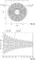
Fig. 2a shows the interference contrast k and unmodulated optical power I/I 0 as functions of the applied voltage and the corresponding phase shift, exemplarily for an ideal reflective BGO voltage sensor, with a 40 nm FWHM Gaussian spectrum centered at 1310 nm, and a group delay offset τ 0 = -60 fs; -
Fig. 2b shows the trace of the MPD-retrieved complex output K = keiϕ of the ideal voltage sensor in the voltage range [-500 kV, 500 kV] in the complex plane; the cross symbol indicates the center of the spiral, which is at the origin of the complex plane; -
Fig. 3a shows traces of the MPD-retrieved complex output K = keiϕ in the voltage range [-500 kV, 500 kV], for a non-ideal voltage sensor with ε F0 = 10° and εθ = 0° and a sensor with ε F0 = 0° and εθ = 10°, respectively; the cross symbols indicate the spiral centers determined by method M1 proposed herein; -
Fig. 3b shows uncompensated phase measurement errors, i.e. arg K - pv(φ 0 + π), for the two non-ideal sensors ofFig. 3a ; -
Fig. 4a shows the traces of the uncompensated K and the compensated K̃, calculated with the proposed method, for a non-ideal sensor with ε F0 = 10° and εθ = 0°; the cross symbols indicate the calculated spiral centers; the compensation parameters are determined with method M1; -
Fig. 4b shows the phase shift errors for the uncompensated, compensated (with method M1), and further optimized (fitted) outputs. - Introduction, device:
The basic principles of the device ofFig. 1 have already been described. - It comprises an
MPD optoelectronics module 1 for generating waves along both polarization directions of a polarization maintaining (PM)fiber 2. Acollimator 3 sends these waves through a 45°Faraday rotator 4 and into a first end ofPockels effect crystal 5, which is being exposed to the electrical field from the voltage to be measured. At the second end of the crystal, the waves are reflected by areflector 6 and sent back through the components 1 - 5 and intoMPD optoelectronics module 1. -
Faraday rotator 4 rotates both linear polarizations fromPM fiber 2 by 45° before they propagate along the electro-optic axes (principal refractive index axes) of sensing crystal 5 [3]. The reflected waves pass throughFaraday rotator 4 again, further rotating the polarizations by 45° in the same direction, thereby making a combined 90° rotation from the input polarizations, which is equivalent to a swap between the two orthogonal linear polarizations. -
MPD optoelectronics module 1 is adapted to measure the interference contrast k as well as the principal value pv of the total phase shift φ between the two polarizations returning fromPM fiber 2, i.e. ϕ = pv(φ) = φ mod 2π. - The
optoelectronics module 1 comprises aphase modulator 7 adapted to introduce a phase shift φm between the two light polarizations returning inPM fiber 2 before they are brought to interference in adetector 8. - It further comprises a
light source 9 generating the light to pass throughPM fiber 2 andcrystal 5. The coherence length oflight source 9 is advantageously between 5·λ 0 and 100·λ 0, with λ 0 being the center wavelength of the light source, in order to obtain a good variation of interference contrast k when changing the phase between the two polarizations by a few multiples of 2π. - The device further comprises a
control unit 10 adapted and structured to carry out the measurement and error compensation methods described below. It can e.g. be formed by a microprocessor or microcontroller provided with suitable interface circuits. - The interference contrast k and principal value ϕ can e.g. be determined e.g. as described in [1].
- In the following, we show that the trace of a complex output with its absolute value equal to the MPD-measured interference contrast k and its argument equal to the MPD-measured phase shift principal value ϕ is a spiral curve in the complex plane. The influence of systematic errors in a reflective optical voltage sensor, such as Faraday rotation angle error and axis alignment error, can be represented as a shift of the spiral center from the complex plane origin, and scaling of the spiral radii along the real and imaginary axes. The systematic measurement error can then be compensated by recentering and rescaling the measured spiral trace, yielding a more accurate phase shift measurement.
- Ideal system with monochromatic light source:
Mathematically, the propagation of polarized light in an ideal voltage sensor between the two passes throughFaraday rotator 3 can be described by a Jones matrix in the basis of the linear polarizations in the PM fiber axes as


PM fiber 2 andsensing crystal 4 electro-optic axes, mirror reflection, the phase delay incrystal 4, the axes rotation and Faraday rotation in the mirrored reference frame, respectively. - Writing out the matrix elements of T, we find

- In a MPD system, a phase modulation φm is added to the optical signal, resulting in a modulated optical power

- With a proper modulation waveform and demodulation scheme, both the phase shift principal value ϕ = arg g 2 and the interference contrast k = |g 2| can be recovered, see e.g. [1]. Contrast k and phase shift principal value ϕ can be combined into a complex value K as

- For the ideal voltage sensor described above, K = -eiφ , so ϕ = pv(φ + π) and k = 1, with pv(x) = x mod 2π called the principal value. The π phase offset in ϕ arises from the mirrored handiness between a 90° rotation and a simple swapping of two orthogonal polarizations.
- The result presented above is valid only for a MPD system operating at a single wavelength. When a low-
coherence light source 9 is used, an ensemble of wavelengths is contained in the broadband spectrum. The spectral dependence of the electro-optic phase shift φ can be expressed as a Taylor series up to the first order
- The detected light power in the MPD system is the ensemble average across the spectrum.

- The MPD-retrieved complex output is then an ensemble average K = keiϕ = 〈g 2〉 = -〈e iφ(ω)〉, where the phase shift principal value is ϕ = pv(φ 0 + π), and the interference contrast k = A(τ + τ 0) = ∫S(ω)e i(τ+τ
0 )(ω-ω0 )dω is the coherence function A(τ) evaluated at group delay τ+τ 0. - If the operating range of the sensor is chosen by selecting a proper group delay offset τ 0 (by means of a birefringent element, e.g. a birefringent crystal) to represent a range where the coherence function A(τ) varies strongly and monotonically, the MPD-retrieved complex output K = keiϕ plotted on the complex plane is a spiral curve emanating from (or converging into) the origin of the complex plane. As an example, for a BGO voltage sensor (π-voltage 75 kV) with a 40 nm FWHM Gaussian spectrum centered at 1310 nm, a suitable choice of τ 0 to cover ±500 kV would be around ±60 fs. In all following calculations, we assume such a spectrum and τ 0 = -60 fs. The phase shift, interference contrast, and the MPD-retrieved complex output trace for the ideal voltage sensor are plotted in
Figs. 2a and 2b . - The situation is, however, more complicated in the presence of systematic errors. For example, the Faraday rotation angle may not be exactly 45°, or the axes of the PM fiber may not be aligned exactly at 45° with the electro-optic axes of the sensing crystal. In such cases, cross-coupling occurs between orthogonal polarizations as the waves enter and exit the sensing crystal, which would disturb the MPD measurement result.
- If we define the Faraday rotation as 45°+εF , (with εF describing the deviation from the ideal 45° rotation) and the angle between the electro-optic axes of the sensing element and the PM fiber axes as 45°+εθ (with εθ describing the deviation from the ideal alignment of the the PM fiber axes), the sensor matrix between the two passes through the Faraday rotator is


- With a broadband spectrum, we should also take into account the wavelength dependence of the Faraday rotation angle. In a Taylor series up to the first order, the Faraday rotation angle deviation can be written as

- For example, for a TGG Faraday rotator, the Faraday rotator angle θF varies according to

- The MPD-retrieved complex variable K =keiϕ , which may be constructed from the MPD-measured phase shift principal value ϕ and interference contrast k, is now, after wavelength-ensemble averaging

- The K traces calculated for two non-ideal voltage sensors are plotted in
Fig. 3a . The traces still have a spiral shape, however with a few important differences from the ideal case: - 1. The spiral center is shifted from the origin of the complex plane along the real axis.
- 2. The radii of the spiral curve change along both real and imaginary axes with different ratios, making the spiral elliptical, i.e. the spiral's real and imaginary amplitudes are scaled.
- Additionally, we note that the signs of ε F0 and εθ do not influence the K trace. With a non-zero ε F0, the spiral is positively shifted along the real axis, while with a non-zero εθ , the spiral is negatively shifted. Therefore, it is possible to compensate the Faraday rotation angle error with a corresponding "misalignment" of the PM fiber axes.
- Generally, in a non-ideal sensor, arg K ≠ pv(φ 0 + π) and |K| ≠ A(τ + τ 0). Therefore, the phase shift calculated using the signal processing scheme described above for an ideal sensor would contain measurement error, which is plotted in
Fig. 3b . A proper compensation method is required in order to reach the required accuracy. - We propose a novel compensation procedure with the following steps:
- 1. Determine, in particular in a calibration measurement, the spiral center K 0 in the complex plane, and the spiral radii in the real and imaginary axes (r 1 and r 2).
- 2. When carrying out a live measurement, shift the spiral center to the complex plane origin, and rescale in both real and imaginary directions. Hence, we calculate a compensated complex output value

- 3. Calculate the compensated phase shift and interference contrast based on the compensated complex output

- The compensated outputs can then be used in the same way as for the outputs from the ideal sensor, i.e.

- The values of K 0 (which is complex valued), r 1 and r 2 (both of which are real-valued) are calibration values, which are determined in a calibration process. For example, in this process, one may vary the applied voltage V in a certain range, and record the complex output K(V) at the same time. The selected voltage range should preferably cover at least one π-voltage for a reflective voltage sensor, whereby the K(V) trace would make at least one full circle around K 0. The selected voltage range should be in a region where the coherence function A(τ + τ 0) is largely linear with the voltage. By proper fitting of the measured K(V) trace to a scaled Archimedes spiral model, the center K 0 and radii (real and imaginary scaling factors) r 1,2 can readily be determined.
- Simpler methods can also work well for the same purpose without requiring computation-intensive curve fitting. Here we give two examples of methods:
- M1.On a full-circle K(V) calibration trace, one may locate the point with the largest real part K r1, the point with the smallest real part K r2, the point with the largest imaginary part K i1, and the point with the smallest imaginary part K i2. Generally, Re(K 0) = Re(K i1) = Re(K i2) and Im(K 0) = Im(K r1) = Im(K r2). One might then set


- M2.In addition to these points, one might additionally use the corresponding points on a subsequent circle (


- Many other implementations can also be used, avoiding curve fitting by making use of a few characteristic points on the spiral to determine its parameters.
-
Fig. 4 shows the comparison between the uncompensated and compensated results, for a non-ideal sensor with ε F0 = 10° and εθ = 0°. The compensation with parameters determined by the simple method M1 results in significant reduction of the phase shift error over the uncompensated result. Further fine adjustment of the calibrated spiral parameters using a fitting method leads to even lower phase shift errors. - According to theoretical calculations, the spiral is expected to shift only along the real axis, i.e. Im K 0 = 0. If the MPD measurement includes an unknown offset due to other systematic errors, the complex output K trace may be rotated about the origin, which would make the spiral center appear shifted also along the imaginary axis. This effect has been observed in some measurements. Such a rotation can be described by replacing Eq. (1) by


- Because the Faraday rotation angle deviation ε F0 and some other parameters (such as the electro-optic coefficient of the sensing crystal) are temperature-dependent, for a voltage sensor operating in a wide temperature range, the above-mentioned calibration (step 1) should be performed at a few representative temperatures in the given range to determine how these parameters vary with temperature. In real operation, a parallel temperature measurement is needed to properly adjust these parameters for the actual operating condition.
- Hence, the present method advantageously comprises the steps of measuring the temperature at
Faraday rotator 4 and selecting the calibration values as a function of this temperature. In this case, the calibration values are advantageously measured for a plurality of temperatures. - In an AC voltage measurement, the instantaneous voltage continuously sweeps along a section of the spiral trace. Therefore, it is possible to do the calibration steps (
step 1 calibration) in real time during a rising or falling slope of the voltage. If the Faraday rotation angle deviation ε F0 has the same sign in the entire temperature range, one may use the temperature dependence of the real-time-calibrated spiral parameters (also optionally the temperature dependence of the group delay offset τ 0) to determine the temperature, and to perform temperature compensation of other parameters, e.g. of the electro-optic coefficient. - Electro-
optic crystal 5 can be replaced by any other electro-optic element that has exhibits a birefringence depending on the applied electrical field. - In general, the calibration values r 1, r 2, and K 0 and, optionally, α, are device-dependent.
- The techniques shown here allow the compensation of systematic errors for an optical DC voltage sensor with measurement range > ±500 kV to achieve an accuracy of < 0.2%.
- They are ideal for applications in HVDC air-insulated systems, HVDC cables, and DC gas-insulated switching (GIS) systems. Such GIS may be filled with dielectric gas based on SF6 or alternative gases, such as fluoroketones or fluoronitriles, preferably in mixtures with a background gas, such as e.g. selected from: nitrogen, carbon dioxide and oxygen.
- They allow to compensate Faraday rotation angle errors and errors in the PM fiber alignment.
- They also allow to compensate systematic errors due to changes in temperature.
- While presently preferred embodiments of the invention are shown and described, it is to be distinctly understood that the invention is not limited thereto but may be otherwise variously embodied and practiced within the scope of the following claims.
-
- [1]
WO 2015/124676 - [2] H. Lefèvre, The Fiber-Optic Gyroscope: Artech House, 1993.
- [3]
US 7911196 . -
- 1:
- MPD optoelectronics module
- 2:
- PM fiber
- 3:
- collimator
- 4:
- Faraday rotator
- 5:
- crystal
- 6:
- reflector
- 7:
- phase modulator
- 8:
- detector
- 9:
- light source
- 10:
- control unit
Claims (11)
- A method for measuring a voltage comprising the steps of:placing an electro-optic element (5) in an electrical field generated by said voltage,passing light from a light source (9) through a Faraday rotator (4) and said electro-optic element (5) onto a reflector (6) and from there back through said electro-optic element (5) and said Faraday rotator (4), thereby generating a voltage-dependent phase shift between two polarizations of said light,measuring an interference contrast k as well as a principal value ϕ of a total phase shift φ between said polarizations,the method characterized bycalculating a corrected interference contrast k̃ and a corrected principal value ϕ̃ from


 and deriving said voltage using said corrected interference contrast k̃ and the corrected principal value ϕ̃.
 - The method of claim 1, further comprising calibration steps comprising:
subjecting said electro-optic element (5) to a varying electrical field,- measuring said interference contrast k as well as said principal value ϕ for several values of said varying electrical field and calculating at least one of said calibration values therefrom. - The method of claim 2, wherein all of said calibration values are calculated in said calibration steps.
- The method of any of the claims 2 or 3, wherein said varying electrical field is varied over a range sufficient to vary a phase shift between said polarizations by at least π, in particular by at least 2π.
- The method of any of the claims 2 to 4, wherein said calibration steps comprise the step of determining a center and real and imaginary scaling factors of a spiral traced by said uncompensated complex value K when varying said principal value ϕ.
- The method of any of the claims 2 to 5, wherein said calibration steps are carried out in a calibration measurement prior to measuring said voltage.
- The method of any of the claims 2 to 5, wherein said voltage is an AC voltage and said calibration steps are carried out during a rising or falling slope of said voltage.
- The method of claim 7, further comprising the step of determining a temperature from said calibration values.
- The method of any of the claims 1 to 6, further comprising the step of measuring a temperature at said Faraday rotator (4) and selecting said calibration values as functions of said temperature.
- A device for measuring a voltage comprising:a Faraday rotator (4),an electro-optic element (5),a reflector (6),a light source (9) positioned to send light through said Faraday rotator (4) and said electro-optic element (5) onto said reflector (6) and from there back through said electro-optic element (5) and said Faraday rotator (4), wherein two polarizations of said light suffer a voltage-dependent phase shift in said electro-optic element,a light detector (8) positioned to measure an interference between said two polarizations returning from that electro-optic element (5) and said Faraday rotator (4),characterized bya control unit (10) adapted and structured to carry out the steps of any of the preceding claims.
- Use of the device or method of any of the preceding claims for measuring a DC voltage of at least 100 kV.
Priority Applications (4)
| Application Number | Priority Date | Filing Date | Title |
|---|---|---|---|
| ES16187127T ES2741848T3 (en) | 2016-09-02 | 2016-09-02 | Interferometric voltage sensor with error compensation |
| EP16187127.2A EP3290931B1 (en) | 2016-09-02 | 2016-09-02 | Interferometric voltage sensor with error compensation |
| CN201710786706.9A CN107796978B (en) | 2016-09-02 | 2017-09-04 | Using the interference-type voltage sensor of error compensation |
| US15/695,858 US11193959B2 (en) | 2016-09-02 | 2017-09-05 | Interferometric voltage sensor with error compensation |
Applications Claiming Priority (1)
| Application Number | Priority Date | Filing Date | Title |
|---|---|---|---|
| EP16187127.2A EP3290931B1 (en) | 2016-09-02 | 2016-09-02 | Interferometric voltage sensor with error compensation |
Publications (2)
| Publication Number | Publication Date |
|---|---|
| EP3290931A1 EP3290931A1 (en) | 2018-03-07 |
| EP3290931B1 true EP3290931B1 (en) | 2019-05-15 |
Family
ID=56855351
Family Applications (1)
| Application Number | Title | Priority Date | Filing Date |
|---|---|---|---|
| EP16187127.2A Not-in-force EP3290931B1 (en) | 2016-09-02 | 2016-09-02 | Interferometric voltage sensor with error compensation |
Country Status (4)
| Country | Link |
|---|---|
| US (1) | US11193959B2 (en) |
| EP (1) | EP3290931B1 (en) |
| CN (1) | CN107796978B (en) |
| ES (1) | ES2741848T3 (en) |
Families Citing this family (2)
| Publication number | Priority date | Publication date | Assignee | Title |
|---|---|---|---|---|
| EP3290931B1 (en) * | 2016-09-02 | 2019-05-15 | ABB Schweiz AG | Interferometric voltage sensor with error compensation |
| CN112859275B (en) * | 2021-01-20 | 2021-12-14 | 中国科学院西安光学精密机械研究所 | Cold optics self-adaptation thermal deformation compensation structure based on Archimedes spiral |
Family Cites Families (39)
| Publication number | Priority date | Publication date | Assignee | Title |
|---|---|---|---|---|
| US4372685A (en) * | 1979-01-15 | 1983-02-08 | Max-Planck-Gesellschaft Zur Forderung Der Wissenschaften E.V. | Method and arrangement for the measurement of rotations |
| JPS5919875A (en) * | 1982-07-27 | 1984-02-01 | Toshiba Corp | Magnetic field measuring device |
| US5309912A (en) * | 1991-11-08 | 1994-05-10 | The United States Of America As Represented By The Secretary Of The Department Of Health And Human Services | Multidimensional imaging using a single point detector for a phase encoded modulated optical carrier |
| US5327213A (en) * | 1991-11-14 | 1994-07-05 | Honeywell Inc. | Configuration control of mode coupling errors |
| US5377283A (en) * | 1992-05-29 | 1994-12-27 | Honeywell Inc. | Configuration control of mode coupling errors |
| US5390023A (en) * | 1992-06-03 | 1995-02-14 | Zygo Corporation | Interferometric method and apparatus to measure surface topography |
| WO1994011708A1 (en) * | 1992-11-06 | 1994-05-26 | Martin Marietta Corporation | Interferometric optical sensor read-out system |
| US5513003A (en) * | 1994-06-06 | 1996-04-30 | Honeywell Inc. | Fiber optic gyro digital control with rate extension |
| JP3708260B2 (en) * | 1996-12-05 | 2005-10-19 | オリンパス株式会社 | Differential interference microscope |
| US6128080A (en) * | 1997-06-06 | 2000-10-03 | Wyatt Technology Corporation | Extended range interferometric refractometer |
| US6246893B1 (en) * | 1997-06-12 | 2001-06-12 | Tecmed Incorporated | Method and device for glucose concentration measurement with special attention to blood glucose determinations |
| US6215295B1 (en) * | 1997-07-25 | 2001-04-10 | Smith, Iii Richard S. | Photonic field probe and calibration means thereof |
| US6078706A (en) * | 1998-09-22 | 2000-06-20 | The United States Of America As Represented By The Secretary Of The Navy | Quasi-static fiber pressure sensor |
| US7557929B2 (en) * | 2001-12-18 | 2009-07-07 | Massachusetts Institute Of Technology | Systems and methods for phase measurements |
| EP1921458A3 (en) * | 2003-07-28 | 2010-09-01 | Nippon Telegraph And Telephone Corporation | Electric field sensor and adjustment method thereof |
| DK1820034T3 (en) * | 2004-11-18 | 2010-02-01 | Powersense As | Compensation of simple fiber optic Faraday power sensors |
| US7414728B2 (en) * | 2004-12-23 | 2008-08-19 | Massachusetts Institute Of Technology | Reconfigurable polarization independent interferometers and methods of stabilization |
| CN101600968B (en) | 2006-12-22 | 2013-01-02 | Abb研究有限公司 | Optical voltage sensor |
| CN101568842B (en) * | 2006-12-22 | 2013-11-20 | Abb研究有限公司 | Optical high voltage sensor |
| DE102007036973A1 (en) * | 2007-02-24 | 2008-09-04 | Fraunhofer-Gesellschaft zur Förderung der angewandten Forschung e.V. | A pixel cell, a method of operating a pixel cell, a method of determining a position of a maximum of an envelope of an analog amplitude modulated signal, a device for determining a charge amount, apparatus and method for determining an amount of charge on a capacitive element, apparatus and method, and setting a circuit node a predetermined voltage, apparatus and method for charge-based analog / digital conversion and apparatus and method for charge-based signal processing |
| EP2233892B1 (en) * | 2009-03-27 | 2015-05-27 | SICK STEGMANN GmbH | Cylindrical Grating Rotation Sensor |
| JP5517583B2 (en) * | 2009-12-07 | 2014-06-11 | キヤノン株式会社 | Aberration measurement system and aberration measurement method |
| JP5904694B2 (en) * | 2009-12-10 | 2016-04-20 | 株式会社東芝 | Sagnac interferometric photocurrent sensor |
| WO2011069558A1 (en) * | 2009-12-11 | 2011-06-16 | Abb Research Ltd | Fiber-optic current sensing using a sensor with exchangeable sub-modules |
| WO2012163924A1 (en) * | 2011-05-27 | 2012-12-06 | Abb Research Ltd | Fiber-optic voltage sensor |
| IN2014DN06677A (en) * | 2012-01-09 | 2015-05-22 | Attochron Llc | |
| GB2500255B (en) * | 2012-03-16 | 2020-04-15 | Oxsensis Ltd | Optical sensor |
| EP2682765A1 (en) * | 2012-07-05 | 2014-01-08 | ABB Research Ltd. | Temperature compensated fiber-optic current sensor |
| CN102981136A (en) * | 2012-11-26 | 2013-03-20 | 东南大学 | Method for calibrating dynamic performances of fiber optical current transducer (FOCT) based on voltage modulation |
| WO2015091972A1 (en) * | 2013-12-20 | 2015-06-25 | Abb Technology Ag | Fiber-optic sensor and method |
| KR102159420B1 (en) * | 2013-12-20 | 2020-09-24 | 에이비비 슈바이쯔 아게 | Optical sensor |
| RU2677126C2 (en) | 2014-02-21 | 2019-01-15 | Абб Швайц Аг | Interferometric sensor |
| WO2015124678A1 (en) * | 2014-02-21 | 2015-08-27 | Abb Technology Ag | Interferometric sensor with differential modulated phase detection |
| JP2015230163A (en) * | 2014-06-03 | 2015-12-21 | 株式会社東芝 | Optical voltage measurement device |
| US9998187B2 (en) * | 2014-10-13 | 2018-06-12 | Nxgen Partners Ip, Llc | System and method for combining MIMO and mode-division multiplexing |
| US9864095B2 (en) * | 2015-06-17 | 2018-01-09 | Halliburton Energy Services, Inc. | Multiplexed microvolt sensor systems |
| US11255663B2 (en) * | 2016-03-04 | 2022-02-22 | May Patents Ltd. | Method and apparatus for cooperative usage of multiple distance meters |
| EP3290931B1 (en) * | 2016-09-02 | 2019-05-15 | ABB Schweiz AG | Interferometric voltage sensor with error compensation |
| EP3290870B1 (en) * | 2016-09-02 | 2019-03-13 | ABB Schweiz AG | Closed-loop interferometric sensor using loop gain for determining interference contrast |
-
2016
- 2016-09-02 EP EP16187127.2A patent/EP3290931B1/en not_active Not-in-force
- 2016-09-02 ES ES16187127T patent/ES2741848T3/en active Active
-
2017
- 2017-09-04 CN CN201710786706.9A patent/CN107796978B/en not_active Expired - Fee Related
- 2017-09-05 US US15/695,858 patent/US11193959B2/en active Active
Non-Patent Citations (1)
| Title |
|---|
| None * |
Also Published As
| Publication number | Publication date |
|---|---|
| US11193959B2 (en) | 2021-12-07 |
| CN107796978A (en) | 2018-03-13 |
| ES2741848T3 (en) | 2020-02-12 |
| CN107796978B (en) | 2019-11-08 |
| EP3290931A1 (en) | 2018-03-07 |
| US20180067147A1 (en) | 2018-03-08 |
Similar Documents
| Publication | Publication Date | Title |
|---|---|---|
| DK3084450T3 (en) | Optical sensor | |
| EP2010925B1 (en) | Fiber-optic current sensor with polarimetric detection scheme | |
| RU2677126C2 (en) | Interferometric sensor | |
| JP2000515979A (en) | Optical fiber device and method for precision current sensing | |
| US10302411B2 (en) | Closed-loop interferometric sensor using loop gain for determining interference contrast | |
| US11193959B2 (en) | Interferometric voltage sensor with error compensation | |
| CN101520323B (en) | Extensive angle measuring method for inclination angle of plane moving mirror in Fourier spectrometer | |
| Zheng et al. | Influences of optical-spectrum errors on excess relative intensity noise in a fiber-optic gyroscope | |
| Kazda et al. | Phase analysis for frequency standards in the microwave and optical domains | |
| WO2015124677A1 (en) | Interferometric sensor | |
| Kumada et al. | Kerr effect in gas and its application to noncontact measurement of electric field | |
| US11143678B2 (en) | Polarization optical detection with enhanced accuracy in the high-signal regime | |
| Aketagawa et al. | Measurement of a free spectral range of a Fabry–Perot cavity using frequency modulation and null method under off-resonance conditions | |
| US20030095262A1 (en) | Optical interferometric sensor with optical error compensation | |
| Bregant et al. | Measurement of the Cotton–Mouton effect in krypton and xenon at 1064 nm with the PVLAS apparatus | |
| Zhi et al. | Error analysis and Stokes parameter measurement of rotating quarter-wave plate polarimeter | |
| Wang et al. | Modeling and experimental verification of polarization errors in Sagnac fiber optic current sensor | |
| Lin et al. | An instrument for measuring low optical rotation angle | |
| Çelikel | Construction and characterization of interferometric fiber optic gyroscope (IFOG) with erbium doped fiber amplifier (EDFA) | |
| Lippa et al. | The GRAVITY metrology system: narrow-angle astrometry via phase-shifting interferometry | |
| Hu et al. | An electro-optic modulator detection method in all optical atomic magnetometer | |
| Gu et al. | Development of an Electro-Optic Voltage Sensor for High Voltage Direct Current Applications | |
| Yang et al. | Digital measuring scheme for half-wave voltage of Y-tap multiple integrated optical circuit | |
| Steiger et al. | Signal processing for electro-optic voltage sensor | |
| Cao et al. | Large optical rotation angles measurement using frequency spectrum analysis |
Legal Events
| Date | Code | Title | Description |
|---|---|---|---|
| PUAI | Public reference made under article 153(3) epc to a published international application that has entered the european phase |
Free format text: ORIGINAL CODE: 0009012 |
|
| STAA | Information on the status of an ep patent application or granted ep patent |
Free format text: STATUS: THE APPLICATION HAS BEEN PUBLISHED |
|
| AK | Designated contracting states |
Kind code of ref document: A1 Designated state(s): AL AT BE BG CH CY CZ DE DK EE ES FI FR GB GR HR HU IE IS IT LI LT LU LV MC MK MT NL NO PL PT RO RS SE SI SK SM TR |
|
| AX | Request for extension of the european patent |
Extension state: BA ME |
|
| STAA | Information on the status of an ep patent application or granted ep patent |
Free format text: STATUS: REQUEST FOR EXAMINATION WAS MADE |
|
| 17P | Request for examination filed |
Effective date: 20180828 |
|
| RBV | Designated contracting states (corrected) |
Designated state(s): AL AT BE BG CH CY CZ DE DK EE ES FI FR GB GR HR HU IE IS IT LI LT LU LV MC MK MT NL NO PL PT RO RS SE SI SK SM TR |
|
| GRAP | Despatch of communication of intention to grant a patent |
Free format text: ORIGINAL CODE: EPIDOSNIGR1 |
|
| STAA | Information on the status of an ep patent application or granted ep patent |
Free format text: STATUS: GRANT OF PATENT IS INTENDED |
|
| RIC1 | Information provided on ipc code assigned before grant |
Ipc: G01R 19/00 20060101ALI20181129BHEP Ipc: G01R 35/00 20060101ALI20181129BHEP Ipc: G01R 15/24 20060101AFI20181129BHEP |
|
| INTG | Intention to grant announced |
Effective date: 20181220 |
|
| GRAS | Grant fee paid |
Free format text: ORIGINAL CODE: EPIDOSNIGR3 |
|
| GRAA | (expected) grant |
Free format text: ORIGINAL CODE: 0009210 |
|
| STAA | Information on the status of an ep patent application or granted ep patent |
Free format text: STATUS: THE PATENT HAS BEEN GRANTED |
|
| RIN1 | Information on inventor provided before grant (corrected) |
Inventor name: BOHNERT, KLAUS Inventor name: MARCHESE, SERGIO VINCENZO Inventor name: GU, XUN |
|
| AK | Designated contracting states |
Kind code of ref document: B1 Designated state(s): AL AT BE BG CH CY CZ DE DK EE ES FI FR GB GR HR HU IE IS IT LI LT LU LV MC MK MT NL NO PL PT RO RS SE SI SK SM TR |
|
| REG | Reference to a national code |
Ref country code: CH Ref legal event code: EP |
|
| REG | Reference to a national code |
Ref country code: DE Ref legal event code: R096 Ref document number: 602016013924 Country of ref document: DE |
|
| REG | Reference to a national code |
Ref country code: IE Ref legal event code: FG4D |
|
| REG | Reference to a national code |
Ref country code: NL Ref legal event code: MP Effective date: 20190515 |
|
| REG | Reference to a national code |
Ref country code: LT Ref legal event code: MG4D |
|
| PG25 | Lapsed in a contracting state [announced via postgrant information from national office to epo] |
Ref country code: NO Free format text: LAPSE BECAUSE OF FAILURE TO SUBMIT A TRANSLATION OF THE DESCRIPTION OR TO PAY THE FEE WITHIN THE PRESCRIBED TIME-LIMIT Effective date: 20190815 Ref country code: FI Free format text: LAPSE BECAUSE OF FAILURE TO SUBMIT A TRANSLATION OF THE DESCRIPTION OR TO PAY THE FEE WITHIN THE PRESCRIBED TIME-LIMIT Effective date: 20190515 Ref country code: LT Free format text: LAPSE BECAUSE OF FAILURE TO SUBMIT A TRANSLATION OF THE DESCRIPTION OR TO PAY THE FEE WITHIN THE PRESCRIBED TIME-LIMIT Effective date: 20190515 Ref country code: HR Free format text: LAPSE BECAUSE OF FAILURE TO SUBMIT A TRANSLATION OF THE DESCRIPTION OR TO PAY THE FEE WITHIN THE PRESCRIBED TIME-LIMIT Effective date: 20190515 Ref country code: PT Free format text: LAPSE BECAUSE OF FAILURE TO SUBMIT A TRANSLATION OF THE DESCRIPTION OR TO PAY THE FEE WITHIN THE PRESCRIBED TIME-LIMIT Effective date: 20190915 Ref country code: SE Free format text: LAPSE BECAUSE OF FAILURE TO SUBMIT A TRANSLATION OF THE DESCRIPTION OR TO PAY THE FEE WITHIN THE PRESCRIBED TIME-LIMIT Effective date: 20190515 Ref country code: NL Free format text: LAPSE BECAUSE OF FAILURE TO SUBMIT A TRANSLATION OF THE DESCRIPTION OR TO PAY THE FEE WITHIN THE PRESCRIBED TIME-LIMIT Effective date: 20190515 Ref country code: AL Free format text: LAPSE BECAUSE OF FAILURE TO SUBMIT A TRANSLATION OF THE DESCRIPTION OR TO PAY THE FEE WITHIN THE PRESCRIBED TIME-LIMIT Effective date: 20190515 |
|
| PG25 | Lapsed in a contracting state [announced via postgrant information from national office to epo] |
Ref country code: LV Free format text: LAPSE BECAUSE OF FAILURE TO SUBMIT A TRANSLATION OF THE DESCRIPTION OR TO PAY THE FEE WITHIN THE PRESCRIBED TIME-LIMIT Effective date: 20190515 Ref country code: BG Free format text: LAPSE BECAUSE OF FAILURE TO SUBMIT A TRANSLATION OF THE DESCRIPTION OR TO PAY THE FEE WITHIN THE PRESCRIBED TIME-LIMIT Effective date: 20190815 Ref country code: RS Free format text: LAPSE BECAUSE OF FAILURE TO SUBMIT A TRANSLATION OF THE DESCRIPTION OR TO PAY THE FEE WITHIN THE PRESCRIBED TIME-LIMIT Effective date: 20190515 Ref country code: GR Free format text: LAPSE BECAUSE OF FAILURE TO SUBMIT A TRANSLATION OF THE DESCRIPTION OR TO PAY THE FEE WITHIN THE PRESCRIBED TIME-LIMIT Effective date: 20190816 |
|
| REG | Reference to a national code |
Ref country code: AT Ref legal event code: MK05 Ref document number: 1134073 Country of ref document: AT Kind code of ref document: T Effective date: 20190515 |
|
| PG25 | Lapsed in a contracting state [announced via postgrant information from national office to epo] |
Ref country code: SK Free format text: LAPSE BECAUSE OF FAILURE TO SUBMIT A TRANSLATION OF THE DESCRIPTION OR TO PAY THE FEE WITHIN THE PRESCRIBED TIME-LIMIT Effective date: 20190515 Ref country code: AT Free format text: LAPSE BECAUSE OF FAILURE TO SUBMIT A TRANSLATION OF THE DESCRIPTION OR TO PAY THE FEE WITHIN THE PRESCRIBED TIME-LIMIT Effective date: 20190515 Ref country code: DK Free format text: LAPSE BECAUSE OF FAILURE TO SUBMIT A TRANSLATION OF THE DESCRIPTION OR TO PAY THE FEE WITHIN THE PRESCRIBED TIME-LIMIT Effective date: 20190515 Ref country code: EE Free format text: LAPSE BECAUSE OF FAILURE TO SUBMIT A TRANSLATION OF THE DESCRIPTION OR TO PAY THE FEE WITHIN THE PRESCRIBED TIME-LIMIT Effective date: 20190515 Ref country code: CZ Free format text: LAPSE BECAUSE OF FAILURE TO SUBMIT A TRANSLATION OF THE DESCRIPTION OR TO PAY THE FEE WITHIN THE PRESCRIBED TIME-LIMIT Effective date: 20190515 |
|
| REG | Reference to a national code |
Ref country code: ES Ref legal event code: FG2A Ref document number: 2741848 Country of ref document: ES Kind code of ref document: T3 Effective date: 20200212 |
|
| REG | Reference to a national code |
Ref country code: DE Ref legal event code: R097 Ref document number: 602016013924 Country of ref document: DE |
|
| PG25 | Lapsed in a contracting state [announced via postgrant information from national office to epo] |
Ref country code: IT Free format text: LAPSE BECAUSE OF FAILURE TO SUBMIT A TRANSLATION OF THE DESCRIPTION OR TO PAY THE FEE WITHIN THE PRESCRIBED TIME-LIMIT Effective date: 20190515 Ref country code: SM Free format text: LAPSE BECAUSE OF FAILURE TO SUBMIT A TRANSLATION OF THE DESCRIPTION OR TO PAY THE FEE WITHIN THE PRESCRIBED TIME-LIMIT Effective date: 20190515 |
|
| PLBE | No opposition filed within time limit |
Free format text: ORIGINAL CODE: 0009261 |
|
| STAA | Information on the status of an ep patent application or granted ep patent |
Free format text: STATUS: NO OPPOSITION FILED WITHIN TIME LIMIT |
|
| PG25 | Lapsed in a contracting state [announced via postgrant information from national office to epo] |
Ref country code: TR Free format text: LAPSE BECAUSE OF FAILURE TO SUBMIT A TRANSLATION OF THE DESCRIPTION OR TO PAY THE FEE WITHIN THE PRESCRIBED TIME-LIMIT Effective date: 20190515 |
|
| 26N | No opposition filed |
Effective date: 20200218 |
|
| PG25 | Lapsed in a contracting state [announced via postgrant information from national office to epo] |
Ref country code: PL Free format text: LAPSE BECAUSE OF FAILURE TO SUBMIT A TRANSLATION OF THE DESCRIPTION OR TO PAY THE FEE WITHIN THE PRESCRIBED TIME-LIMIT Effective date: 20190515 |
|
| PG25 | Lapsed in a contracting state [announced via postgrant information from national office to epo] |
Ref country code: SI Free format text: LAPSE BECAUSE OF FAILURE TO SUBMIT A TRANSLATION OF THE DESCRIPTION OR TO PAY THE FEE WITHIN THE PRESCRIBED TIME-LIMIT Effective date: 20190515 Ref country code: MC Free format text: LAPSE BECAUSE OF FAILURE TO SUBMIT A TRANSLATION OF THE DESCRIPTION OR TO PAY THE FEE WITHIN THE PRESCRIBED TIME-LIMIT Effective date: 20190515 |
|
| REG | Reference to a national code |
Ref country code: CH Ref legal event code: PL |
|
| PG25 | Lapsed in a contracting state [announced via postgrant information from national office to epo] |
Ref country code: LU Free format text: LAPSE BECAUSE OF NON-PAYMENT OF DUE FEES Effective date: 20190902 Ref country code: IE Free format text: LAPSE BECAUSE OF NON-PAYMENT OF DUE FEES Effective date: 20190902 Ref country code: LI Free format text: LAPSE BECAUSE OF NON-PAYMENT OF DUE FEES Effective date: 20190930 Ref country code: CH Free format text: LAPSE BECAUSE OF NON-PAYMENT OF DUE FEES Effective date: 20190930 |
|
| REG | Reference to a national code |
Ref country code: BE Ref legal event code: MM Effective date: 20190930 |
|
| PG25 | Lapsed in a contracting state [announced via postgrant information from national office to epo] |
Ref country code: BE Free format text: LAPSE BECAUSE OF NON-PAYMENT OF DUE FEES Effective date: 20190930 |
|
| PG25 | Lapsed in a contracting state [announced via postgrant information from national office to epo] |
Ref country code: RO Free format text: LAPSE BECAUSE OF FAILURE TO SUBMIT A TRANSLATION OF THE DESCRIPTION OR TO PAY THE FEE WITHIN THE PRESCRIBED TIME-LIMIT Effective date: 20190515 |
|
| REG | Reference to a national code |
Ref country code: DE Ref legal event code: R081 Ref document number: 602016013924 Country of ref document: DE Owner name: ABB POWER GRIDS SWITZERLAND AG, CH Free format text: FORMER OWNER: ABB SCHWEIZ AG, BADEN, CH |
|
| REG | Reference to a national code |
Ref country code: ES Ref legal event code: PC2A Owner name: ABB POWER GRIDS SWITZERLAND AG Effective date: 20210520 |
|
| PG25 | Lapsed in a contracting state [announced via postgrant information from national office to epo] |
Ref country code: CY Free format text: LAPSE BECAUSE OF FAILURE TO SUBMIT A TRANSLATION OF THE DESCRIPTION OR TO PAY THE FEE WITHIN THE PRESCRIBED TIME-LIMIT Effective date: 20190515 |
|
| PG25 | Lapsed in a contracting state [announced via postgrant information from national office to epo] |
Ref country code: IS Free format text: LAPSE BECAUSE OF FAILURE TO SUBMIT A TRANSLATION OF THE DESCRIPTION OR TO PAY THE FEE WITHIN THE PRESCRIBED TIME-LIMIT Effective date: 20190915 |
|
| PG25 | Lapsed in a contracting state [announced via postgrant information from national office to epo] |
Ref country code: MT Free format text: LAPSE BECAUSE OF FAILURE TO SUBMIT A TRANSLATION OF THE DESCRIPTION OR TO PAY THE FEE WITHIN THE PRESCRIBED TIME-LIMIT Effective date: 20190515 Ref country code: HU Free format text: LAPSE BECAUSE OF FAILURE TO SUBMIT A TRANSLATION OF THE DESCRIPTION OR TO PAY THE FEE WITHIN THE PRESCRIBED TIME-LIMIT; INVALID AB INITIO Effective date: 20160902 |
|
| PGFP | Annual fee paid to national office [announced via postgrant information from national office to epo] |
Ref country code: FR Payment date: 20210922 Year of fee payment: 6 |
|
| PGFP | Annual fee paid to national office [announced via postgrant information from national office to epo] |
Ref country code: GB Payment date: 20210920 Year of fee payment: 6 Ref country code: DE Payment date: 20210920 Year of fee payment: 6 |
|
| REG | Reference to a national code |
Ref country code: GB Ref legal event code: 732E Free format text: REGISTERED BETWEEN 20211104 AND 20211110 |
|
| PGFP | Annual fee paid to national office [announced via postgrant information from national office to epo] |
Ref country code: ES Payment date: 20211125 Year of fee payment: 6 |
|
| PG25 | Lapsed in a contracting state [announced via postgrant information from national office to epo] |
Ref country code: MK Free format text: LAPSE BECAUSE OF FAILURE TO SUBMIT A TRANSLATION OF THE DESCRIPTION OR TO PAY THE FEE WITHIN THE PRESCRIBED TIME-LIMIT Effective date: 20190515 |
|
| REG | Reference to a national code |
Ref country code: DE Ref legal event code: R119 Ref document number: 602016013924 Country of ref document: DE |
|
| GBPC | Gb: european patent ceased through non-payment of renewal fee |
Effective date: 20220902 |
|
| PG25 | Lapsed in a contracting state [announced via postgrant information from national office to epo] |
Ref country code: FR Free format text: LAPSE BECAUSE OF NON-PAYMENT OF DUE FEES Effective date: 20220930 Ref country code: DE Free format text: LAPSE BECAUSE OF NON-PAYMENT OF DUE FEES Effective date: 20230401 |
|
| REG | Reference to a national code |
Ref country code: ES Ref legal event code: FD2A Effective date: 20231026 |
|
| PG25 | Lapsed in a contracting state [announced via postgrant information from national office to epo] |
Ref country code: GB Free format text: LAPSE BECAUSE OF NON-PAYMENT OF DUE FEES Effective date: 20220902 |
|
| PG25 | Lapsed in a contracting state [announced via postgrant information from national office to epo] |
Ref country code: ES Free format text: LAPSE BECAUSE OF NON-PAYMENT OF DUE FEES Effective date: 20220903 |
|
| PG25 | Lapsed in a contracting state [announced via postgrant information from national office to epo] |
Ref country code: ES Free format text: LAPSE BECAUSE OF NON-PAYMENT OF DUE FEES Effective date: 20220903 |