EP3276585A1 - Active thermal sensor adapted to large pixels - Google Patents
Active thermal sensor adapted to large pixels Download PDFInfo
- Publication number
- EP3276585A1 EP3276585A1 EP17183887.3A EP17183887A EP3276585A1 EP 3276585 A1 EP3276585 A1 EP 3276585A1 EP 17183887 A EP17183887 A EP 17183887A EP 3276585 A1 EP3276585 A1 EP 3276585A1
- Authority
- EP
- European Patent Office
- Prior art keywords
- pixels
- pixel
- pyroelectric
- electrodes
- portions
- Prior art date
- Legal status (The legal status is an assumption and is not a legal conclusion. Google has not performed a legal analysis and makes no representation as to the accuracy of the status listed.)
- Granted
Links
- 238000010438 heat treatment Methods 0.000 claims abstract description 116
- 239000000463 material Substances 0.000 claims abstract description 58
- 238000005259 measurement Methods 0.000 claims abstract description 12
- 238000001514 detection method Methods 0.000 claims description 61
- 239000011159 matrix material Substances 0.000 claims description 15
- 239000002033 PVDF binder Substances 0.000 claims description 9
- 238000000034 method Methods 0.000 claims description 9
- 229920002981 polyvinylidene fluoride Polymers 0.000 claims description 9
- 239000003990 capacitor Substances 0.000 claims description 8
- 230000000694 effects Effects 0.000 claims description 8
- 238000007639 printing Methods 0.000 claims description 7
- 239000004020 conductor Substances 0.000 claims description 6
- 230000008021 deposition Effects 0.000 claims description 3
- 238000005485 electric heating Methods 0.000 claims description 2
- 238000005530 etching Methods 0.000 claims description 2
- 230000008569 process Effects 0.000 claims description 2
- 239000010410 layer Substances 0.000 description 58
- 230000008901 benefit Effects 0.000 description 9
- 239000000758 substrate Substances 0.000 description 9
- 238000005516 engineering process Methods 0.000 description 7
- 230000010354 integration Effects 0.000 description 6
- 239000000976 ink Substances 0.000 description 5
- 238000004519 manufacturing process Methods 0.000 description 5
- 239000011241 protective layer Substances 0.000 description 5
- BQCADISMDOOEFD-UHFFFAOYSA-N Silver Chemical compound [Ag] BQCADISMDOOEFD-UHFFFAOYSA-N 0.000 description 4
- 230000005684 electric field Effects 0.000 description 4
- 230000035945 sensitivity Effects 0.000 description 4
- 229910052709 silver Inorganic materials 0.000 description 4
- 239000004332 silver Substances 0.000 description 4
- 229910052727 yttrium Inorganic materials 0.000 description 4
- 229920000139 polyethylene terephthalate Polymers 0.000 description 3
- 239000005020 polyethylene terephthalate Substances 0.000 description 3
- OKTJSMMVPCPJKN-UHFFFAOYSA-N Carbon Chemical compound [C] OKTJSMMVPCPJKN-UHFFFAOYSA-N 0.000 description 2
- 229920001609 Poly(3,4-ethylenedioxythiophene) Polymers 0.000 description 2
- 239000004642 Polyimide Substances 0.000 description 2
- 239000000853 adhesive Substances 0.000 description 2
- 230000001070 adhesive effect Effects 0.000 description 2
- 229910052799 carbon Inorganic materials 0.000 description 2
- 230000008859 change Effects 0.000 description 2
- 239000004744 fabric Substances 0.000 description 2
- 229910052751 metal Inorganic materials 0.000 description 2
- 239000002184 metal Substances 0.000 description 2
- 239000004033 plastic Substances 0.000 description 2
- 229920003023 plastic Polymers 0.000 description 2
- 230000010287 polarization Effects 0.000 description 2
- 229920003207 poly(ethylene-2,6-naphthalate) Polymers 0.000 description 2
- -1 polyethylene naphthalate Polymers 0.000 description 2
- 239000011112 polyethylene naphthalate Substances 0.000 description 2
- 229920001721 polyimide Polymers 0.000 description 2
- 239000010409 thin film Substances 0.000 description 2
- 238000006677 Appel reaction Methods 0.000 description 1
- 229920002799 BoPET Polymers 0.000 description 1
- RYGMFSIKBFXOCR-UHFFFAOYSA-N Copper Chemical compound [Cu] RYGMFSIKBFXOCR-UHFFFAOYSA-N 0.000 description 1
- 230000003416 augmentation Effects 0.000 description 1
- 230000015572 biosynthetic process Effects 0.000 description 1
- 239000011248 coating agent Substances 0.000 description 1
- 238000000576 coating method Methods 0.000 description 1
- 239000012141 concentrate Substances 0.000 description 1
- 238000001816 cooling Methods 0.000 description 1
- 229920001577 copolymer Polymers 0.000 description 1
- 229910052802 copper Inorganic materials 0.000 description 1
- 239000010949 copper Substances 0.000 description 1
- PMHQVHHXPFUNSP-UHFFFAOYSA-M copper(1+);methylsulfanylmethane;bromide Chemical compound Br[Cu].CSC PMHQVHHXPFUNSP-UHFFFAOYSA-M 0.000 description 1
- 229910003460 diamond Inorganic materials 0.000 description 1
- 239000010432 diamond Substances 0.000 description 1
- 238000006073 displacement reaction Methods 0.000 description 1
- 238000005538 encapsulation Methods 0.000 description 1
- 239000011521 glass Substances 0.000 description 1
- 239000003292 glue Substances 0.000 description 1
- 230000002452 interceptive effect Effects 0.000 description 1
- 238000001459 lithography Methods 0.000 description 1
- 239000007769 metal material Substances 0.000 description 1
- 230000003071 parasitic effect Effects 0.000 description 1
- 230000035699 permeability Effects 0.000 description 1
- 230000004224 protection Effects 0.000 description 1
- 238000011084 recovery Methods 0.000 description 1
- 230000009467 reduction Effects 0.000 description 1
- 239000004065 semiconductor Substances 0.000 description 1
- 239000002356 single layer Substances 0.000 description 1
- 229910000679 solder Inorganic materials 0.000 description 1
- 239000004753 textile Substances 0.000 description 1
- 238000011144 upstream manufacturing Methods 0.000 description 1
- XLYOFNOQVPJJNP-UHFFFAOYSA-N water Substances O XLYOFNOQVPJJNP-UHFFFAOYSA-N 0.000 description 1
Images


Classifications
-
- G—PHYSICS
- G08—SIGNALLING
- G08B—SIGNALLING OR CALLING SYSTEMS; ORDER TELEGRAPHS; ALARM SYSTEMS
- G08B21/00—Alarms responsive to a single specified undesired or abnormal condition and not otherwise provided for
- G08B21/02—Alarms for ensuring the safety of persons
- G08B21/04—Alarms for ensuring the safety of persons responsive to non-activity, e.g. of elderly persons
- G08B21/0438—Sensor means for detecting
- G08B21/0461—Sensor means for detecting integrated or attached to an item closely associated with the person but not worn by the person, e.g. chair, walking stick, bed sensor
-
- G—PHYSICS
- G01—MEASURING; TESTING
- G01J—MEASUREMENT OF INTENSITY, VELOCITY, SPECTRAL CONTENT, POLARISATION, PHASE OR PULSE CHARACTERISTICS OF INFRARED, VISIBLE OR ULTRAVIOLET LIGHT; COLORIMETRY; RADIATION PYROMETRY
- G01J5/00—Radiation pyrometry, e.g. infrared or optical thermometry
- G01J5/0022—Radiation pyrometry, e.g. infrared or optical thermometry for sensing the radiation of moving bodies
- G01J5/0025—Living bodies
-
- G—PHYSICS
- G01—MEASURING; TESTING
- G01J—MEASUREMENT OF INTENSITY, VELOCITY, SPECTRAL CONTENT, POLARISATION, PHASE OR PULSE CHARACTERISTICS OF INFRARED, VISIBLE OR ULTRAVIOLET LIGHT; COLORIMETRY; RADIATION PYROMETRY
- G01J5/00—Radiation pyrometry, e.g. infrared or optical thermometry
- G01J5/10—Radiation pyrometry, e.g. infrared or optical thermometry using electric radiation detectors
- G01J5/34—Radiation pyrometry, e.g. infrared or optical thermometry using electric radiation detectors using capacitors, e.g. pyroelectric capacitors
-
- G—PHYSICS
- G01—MEASURING; TESTING
- G01K—MEASURING TEMPERATURE; MEASURING QUANTITY OF HEAT; THERMALLY-SENSITIVE ELEMENTS NOT OTHERWISE PROVIDED FOR
- G01K7/00—Measuring temperature based on the use of electric or magnetic elements directly sensitive to heat ; Power supply therefor, e.g. using thermoelectric elements
- G01K7/003—Measuring temperature based on the use of electric or magnetic elements directly sensitive to heat ; Power supply therefor, e.g. using thermoelectric elements using pyroelectric elements
-
- G—PHYSICS
- G06—COMPUTING; CALCULATING OR COUNTING
- G06V—IMAGE OR VIDEO RECOGNITION OR UNDERSTANDING
- G06V10/00—Arrangements for image or video recognition or understanding
- G06V10/10—Image acquisition
- G06V10/12—Details of acquisition arrangements; Constructional details thereof
-
- G—PHYSICS
- G06—COMPUTING; CALCULATING OR COUNTING
- G06V—IMAGE OR VIDEO RECOGNITION OR UNDERSTANDING
- G06V20/00—Scenes; Scene-specific elements
- G06V20/50—Context or environment of the image
- G06V20/52—Surveillance or monitoring of activities, e.g. for recognising suspicious objects
-
- G—PHYSICS
- G08—SIGNALLING
- G08B—SIGNALLING OR CALLING SYSTEMS; ORDER TELEGRAPHS; ALARM SYSTEMS
- G08B21/00—Alarms responsive to a single specified undesired or abnormal condition and not otherwise provided for
- G08B21/02—Alarms for ensuring the safety of persons
- G08B21/04—Alarms for ensuring the safety of persons responsive to non-activity, e.g. of elderly persons
- G08B21/0407—Alarms for ensuring the safety of persons responsive to non-activity, e.g. of elderly persons based on behaviour analysis
- G08B21/043—Alarms for ensuring the safety of persons responsive to non-activity, e.g. of elderly persons based on behaviour analysis detecting an emergency event, e.g. a fall
-
- G—PHYSICS
- G01—MEASURING; TESTING
- G01J—MEASUREMENT OF INTENSITY, VELOCITY, SPECTRAL CONTENT, POLARISATION, PHASE OR PULSE CHARACTERISTICS OF INFRARED, VISIBLE OR ULTRAVIOLET LIGHT; COLORIMETRY; RADIATION PYROMETRY
- G01J5/00—Radiation pyrometry, e.g. infrared or optical thermometry
- G01J5/10—Radiation pyrometry, e.g. infrared or optical thermometry using electric radiation detectors
- G01J2005/106—Arrays
Definitions
- the invention relates to an active thermal detection device with pyroelectric capacitors whose structure is adapted for large pixels.
- the invention applies in particular to the production of a device for detecting a large thermal mass, for example of a human being or of an animal, and used, for example, to detect the presence and / or movements and / or the position of a person in a bed, or placed on or in the ground to detect the presence and / or movements and / or position of a person on that ground, for example to detect a fall of that person.
- WO 2014/037016 A1 discloses a detection device using the piezoelectric and pyroelectric effect for detecting a surface on which this device is located.
- each pixel comprises a pyroelectric capacitance formed of two conductive electrodes between which a portion of pyroelectric material is disposed, and a heating element.
- This heating element dissipates a certain amount of heat in the pixel, and the heating of the pixel is measured after a certain acquisition time, called integration time, in the presence of the finger on the sensor.
- such a sensor can measure the heat capacity, also called specific heat or specific heat capacity, of an element in contact with the sensor.
- the measurements obtained also depend on the thermal conductivity between the sensor and the part of the element (peak or valley in the case of a fingerprint) in the presence.
- the pixels of this sensor are coupled to heating elements generally using the Joule effect which dissipates heat from a resistive element which is traversed by a current.
- One of the levels of the technological stack forming the pixels is advantageously used to form these heating elements.
- the sensor comprises transistors of the TFT ("Thin-Film Transistor" or thin-film transistor) type produced on a glass or plastic substrate.
- the pixels of such a sensor are arranged by forming a matrix of several rows and several columns of pixels.
- the reading of the pixels is generally done line by line.
- the heating elements can then also be controlled line by line using a transistor at the top of each line, thus avoiding the addition of control transistors in each of the pixels.
- Each line of heating elements is for example connected, on one side of the pixel matrix, to ground, and on the other side to the control transistor associated with the pixel line and connected to a power supply adapted to control the current flowing through the heating elements, and therefore the thermal power injected by the Joule effect into the pixels by these heating elements.
- each of the pixels comprises at least one selection transistor, and the selection transistors of the pixels of each column of pixels are connected. to a conductive line itself connected to a read circuit.
- the selection transistors of the pixels of this line are set to the on state, which makes it possible to connect the active nodes of the pixels of this line to the reading circuits at the foot of the line.
- Blocked selection transistors of the pixels belonging to the other pixel lines prevent the displacement of charges from these other pixels to the readout circuits.
- transistors may also be present in each pixel, especially when the pixels are read in voltage and they require the presence of a reset transistor and a voltage follower transistor, or the sensor also forms a sensor wherein a transistor is present in each pixel for connecting a photodiode of each pixel to a dedicated read circuit.
- the active thermal detection has many advantages over other techniques used to perform for example a person detection in a bed or on a floor (such as obtaining a stable signal level independent of the temperature of the person because it is mainly its thermal mass, associated with its thermal conductivity, which is involved in an active thermal detection), the structure of these fingerprint sensors is not suitable for realizing a person detection because of dimensions of the device necessary for its realization. Indeed, a fingerprint sensor usually uses pixels having a pitch equal to about 50 microns, which is not compatible and unnecessary, with a detection device having dimensions of the order of one meter.
- the thicknesses of the surface protections of a person detection device are of the order of one or several millimeters, which is much too important for a device having pixels made with a pitch equal to about 50 ⁇ m. .
- the presence of the transistors within the pixels is also constraining for the realization of a person detection device because the realization of these transistors requires the implementation of additional deposits of materials, these deposits being expensive.
- An object of the present invention is to provide an active thermal detection device, that is to say having pixels heating elements, pyroelectric capacitors, which is adapted to be made with pixels of large size, thereby providing the advantages of the active thermal detection device for example adapted to the detection of a person or an animal when the latter or it is on this device, and which does not require the presence of transistors within the pixels.
- each heating element is able to be controlled individually, that is to say independently of the heating elements associated with the other pixels.
- the implementation of active thermal detection has the advantage, compared to a passive thermal detection, of detecting the presence of a thermal mass and not only a thermal change as is the case for passive thermal detection, c i.e. without heating means.
- Large pixels correspond for example to pixels of dimensions of between about 1 cm and 10 cm side, and / or made with a pitch for example of the order of 10 cm or between about 5 cm and 50 cm.
- the reading electrodes are formed by a first electrically conductive layer common to all the pixels of the matrix and in contact with the pyroelectric material portions of the pixels of the matrix. This feature is possible because the heating elements are individually addressable.
- the reading electronics used with such a device can therefore comprise a single input, thus greatly simplifying its implementation and making it compatible with the applications envisaged for large pixels.
- Another advantage related to the fact that the heaters are individually addressable is that the resolution of the device can easily be changed by heating several pixels simultaneously.
- such a device can be used as a presence detector of a person, for example in a bed.
- the device is made in the form of a web to be arranged between the mattress and a sheet covering the mattress and for detecting the presence or absence of a person, or its position in the bed.
- Such a device can also be placed on or in a floor, for example under a floor, to detect the presence and / or movements of a person on the floor, for example a fall.
- Such a device can also be used to detect a presence of a person on a seat, the device can in this case be arranged under the seat fabric.
- Such a device can also be placed on or in a steering wheel (or more generally any guiding means) of a vehicle to detect that a person holds the steering wheel.
- Such a device can also be used to detect water, ice or snow on a floor, a roof, etc.
- Such a device can also be used to count a number of people on a floor.
- This sensor corresponds to an active sensor (because comprising heated pixels) made with a set of passive pixels, that is to say without transistors present within the pixels.
- the realization of this sensor is not limited by the technology necessary for producing transistors within the pixels, and can be achieved in printed technology, for example on a flexible substrate.
- pixel fabrication is simplified and boils down to the ability to achieve the heating elements and connection elements of these heating elements at the desired resolution. This becomes possible with less expensive processes than semiconductor lithography, such as deposits by printing.
- the different conductive portions forming the elements of the pixels of the sensor can be made with conductive inks sufficiently stable not to require high performance encapsulation.
- the realization of the sensor is possible by printing, for example on simple plastic substrates (PET films).
- Such a sensor also has the advantage of reducing the number of signals necessary for its control because the selection of the read pixel is performed via the heating of this pixel.
- the sensor further comprises a read circuit to which the reading electrodes are connected.
- the pixels may together form a detection surface having a width of between about 0.5 m and 2 m and a length of between about 1 m and 10 m, or a detection surface of between about 0.5 m 2 and 10 m. m 2 , and / or each pixel can form a detection surface having sides each of dimension between about 1 cm and 10 cm, or a detection surface of between about 1 cm 2 and 100 cm 2 , and / or the device may have a number of pixels between about 25 and 250.
- a second of the lower and upper electrodes of each pixel may be formed by a second electrically conductive layer common to all the pixels and adapted to be electrically connected to an electrical reference potential.
- a single pyroelectric capacitance is common to all the pixels of the matrix, thus simplifying the realization of the device.
- the second electrically conductive layer may be disposed between the heating elements and the reading electrodes.
- the second electrically conductive layer forms both the upper electrodes of the pixels and an electromagnetic shielding layer of the device.
- the device may further comprise a dielectric layer covering the upper electrodes of the pixels and on which the heating elements are arranged.
- Each heating element may comprise one or more portions of material forming a resistive element disposed vertically above a portion of the pyroelectric capacitance of the pixel and of which first and second ends are electrically connected, via first and second tracks. electrically conductive, to an electronic control circuit capable of circulating an electric heating current in each resistive element individually as it heats by Joule effect the pyroelectric capacitance of the pixel.
- each resistive element may comprise one or more portions of resistive material of smaller section than the first and second conductive tracks, and for example arranged in a serpentine pattern, and / or the material of the portion or portions forming each resistive element has a higher resistivity than a material of the first and second electrically conductive tracks.
- each resistive element can be electrically connected to the electronic control circuit via one of the first electrically conductive tracks distinct from the other first electrically conductive tracks electrically connecting the first ends of the other resistive elements to the electronic control circuit, and / or the second ends of the pixel resistive elements can be electrically connected to the electronic control circuit via the second electrically conductive tracks which are electrically connected to each other.
- the second electrically conductive tracks can be connected to ground.
- Parts of the layers forming the lower and upper electrodes of the pixels and portions of the first and second electrically conductive tracks may not be covered by other materials and may form electrical accesses to the lower and upper electrodes and the heating elements.
- the first electrically conductive layer may be etched as it comprises first portions located under the heating elements and forming the reading electrodes of the pixels, and the second portions connecting electrically between them the first portions. This configuration makes it possible to reduce the value of the pyroelectric capacitance of the pixels.
- the device may further comprise holes passing through the device. These holes impart permeability to the humidity of the device and also reduce the value of the pyroelectric capacitance of the pixels.
- the pyroelectric material may be PVDF or P (VDF-TrFE), and / or the pixels may be arranged next to one another forming a matrix of several rows and columns.
- the realization of the lower electrodes of the pixels and / or the upper electrodes of the pixels and / or the pixel heating elements may comprise the implementation of at least one deposition by printing of at least one electrically conductive material.
- the deposit by printing has the advantage of greatly reducing the cost associated with the production of the device.
- the realization of the pyroelectric capacitance of each pixel can comprise the implementation of an etching of the first layer electrically conductive such that remaining portions of the first electrically conductive layer form first portions located under the heating elements and forming the reading electrodes of the pixels, and second portions electrically interconnecting the first portions.
- the method also comprises producing a reading circuit to which the reading electrodes are connected.
- FIG. 1 represents a sectional view of a pixel 102 of an active thermal detection device 100.
- the pixel 102 is formed on a substrate 104 corresponding for example to a flexible substrate, for example based on polyimide or PEN (polyethylene naphthalate) or PET (polyethylene terephthalate), on which the electrical elements of the sensor 100 are made by technology printed (for example via an embodiment with ink jet type writing heads).
- the thickness of the substrate 104 is for example equal to about 125 microns or more generally between about 50 microns and 250 microns.
- the pixels 102 of the sensor 100 are here arranged forming a matrix of several lines and several columns of pixels 102.
- the pitch of the pixels 102, in the plane (X, Y) is for example equal to about 10 cm (for pixels of dimension 10 x 10 cm in the (X, Y) plane), or between about 10 cm and 20 cm, or more generally between about 5 cm and 50 cm. cm.
- the pixels 102 may be evenly distributed over the entire detection surface of the device 100. However, it is possible not to have pixels 102 at the edges of the device 100. In general, it is possible for the distribution pixels 102 on the entire detection surface of the device 100 is not uniform, some regions of the device 100 may be more or less dense than the rest of the surface of the device 100.
- the detection surface of the device (corresponding to the surface in the plane (X, Y) of the different figures) is for example between about 0.5 mx 1 m and 2 mx 2 m .
- each pixel may form a detection surface having dimension sides of between about 1 cm and 10 cm.
- the device 100 may comprise a number of pixels between approximately 25 and 250.
- Each of the pixels 102 of the sensor 100 comprises measurement means, or detection, thermal formed by a pyroelectric capacitance.
- Each pyroelectric capacitor comprises a portion 106 of pyroelectric material disposed between a lower electrode 108 and an upper electrode 110.
- the pyroelectric material of the portion 106 is here a copolymer, advantageously P (VDF-TrFE) or PVDF.
- the pyroelectric material of the portion 106 may be AIN or PZT, or any other pyroelectric material adapted to form a pyroelectric capacitance.
- the thickness of the portion 106 is for example equal to about 3 microns, and for example between about 2 and 10 microns.
- the electrodes 108, 110 each comprise at least one electrically conductive material, for example a metallic material such as silver, copper, carbon or PEDOT (poly (3,4-ethylenedioxythiophene) in the form of ink
- the thickness of each of the electrodes 108, 110 is, for example, approximately 5 ⁇ m or approximately between 10 ⁇ m and 10 ⁇ m.
- the lower electrodes 108 are formed by a first electrically conductive layer 109, here metallic, common to all the pixels 102 of the matrix 100.
- the upper electrodes 110 are formed by a second electrically conductive layer 111, here metallic, common to all the pixels 102 of the matrix 100.
- the portions 106 of pyroelectric material of all the pixels of the matrix of the sensor 100 are also made in the form of a single layer of pyroelectric material 113 covering the first layer 109 which forms the lower electrodes 108.
- the second layer 111 which forms the upper electrodes 110 covers this layer of pyroelectric material 113.
- the first and second layers 109, 111 as well as the layer of pyroelectric material 113 are therefore continuous, that is to say they are not interrupted between the pixels 102.
- the second layer 111 forms an electromagnetic shielding within the stack of layers of the device 100, thus avoiding the recovery of electromagnetic noise (for example 50 Hz noise from the sector) in the measurements made. This second layer 111 also protects the device 100 against electrostatic discharge (ESD).
- ESD electrostatic discharge
- the second layer 111 is covered by a dielectric layer 112 of thickness for example equal to about 3 microns or between about 3 microns and 5 microns, and on which heating elements 114 of the pixels 102 are made.
- Each of the heating elements 114 forms a resistive metal element (electrical resistance for example between approximately 10 ⁇ and 100 ⁇ ) associated with a pixel 102 and which makes it possible to heat this pixel 102 independently of the heating elements 114 associated with the other pixels 102.
- heaters 114 enable, during a detection implemented by the device 100, to dissipate a certain amount of heat in the pixels 102, and in particular in the pyroelectric material of the layer 113.
- the heating of the portion 106 of pyroelectric material is obtained by circulating a current in the heating element 114 forming the heating resistor of each of the pixels 102.
- the heating elements 114 are for example made by a deposition of a metallic ink, comprising for example silver deposited by printing with a thickness of about 5 ⁇ m or between about 1 ⁇ m and 10 ⁇ m.
- the heating elements 114 as well as the portions of the dielectric layer 112 on which the heating elements 114 are not present are covered by a protective layer 116, corresponding for example to a laminated layer of PET or of any other material suitable for carrying out of this layer.
- the thickness of the protective layer 116 may be between a few microns (for example 5 ⁇ m) and about 100 ⁇ m, for example equal to about 50 ⁇ m, or be larger (for example of the order of 300 ⁇ m or more). In the embodiment described here, the thickness of the protective layer 116 is equal to about 25 microns.
- the protective layer 116 may correspond to a layer of DLC (Diamond Like Carbon) with a thickness of less than about 1 ⁇ m.
- An upper face 118 of the protective layer 116 corresponds to the surface above which the thermal detection is intended to be carried out.
- this upper face 118 forms the surface on which the presence of a person is intended to be detected.
- this material is subjected, once for the entire lifetime of the pyroelectric capacitor, to an electric field of approximately 100 volts per micron of thickness. of PVDF.
- the molecules inside the PVDF orient, and remain oriented, even when the PVDF is no longer subject to this electric field.
- the PVDF can thus be polarized by applying an initial bias voltage across the electrodes 108, 110.
- the parameter S corresponds to the surface of the portion 106 facing each of the heating elements.
- the parameter ⁇ corresponds to the pyroelectric coefficient of the pyroelectric material of the portion 106.
- the pyroelectric coefficient ⁇ of the PVFD-TrFE is equal to approximately 32 ⁇ C / m 2 / K.
- the pyroelectric capacitance is common to all the pixels 102 of the device.
- the distinction between the read pixels is due to the fact that the heating elements 114 are individually addressable.
- the direction of the current obtained between the electrodes 108, 110 depends on the direction of the electric field with which the PVDF of the portion 106 was initially polarized. In the case of certain other pyroelectric materials such as aluminum nitride, this direction of initial polarization depends on the manner in which the pyroelectric material has been deposited, its order and its crystallographic orientation. In addition, the direction of the current obtained may vary depending on whether the temperature variation experienced by the pyroelectric capacitance is positive or negative.
- all the material layers of the device 100 may be deposited by printing.
- the figure 2 represents a top view of a portion of the device 100 according to a first embodiment. In this figure, only the dielectric layer 112 and the heating elements 114 disposed on the dielectric layer 112 are shown.
- the device 100 corresponds to a person detection device adapted to carry out a detection of a person in a bed.
- the device 100 is here intended to be arranged on a mattress and under a sheet of textile material with a thickness for example of the order of a few hundred microns to 1 mm.
- the device 100 here has a length "b" equal to about 190 cm and a width "c" equal to about 90 cm. These values can of course differ according to the desired dimensions (smaller for example for a cradle or an incubator).
- the heating elements 114 correspond to resistive elements each comprising, for a pixel 102, a portion of resistive conductive material arranged in a serpentine pattern, and thus able to heat the portion of pyroelectric material by Joule effect. of this pixel 102.
- Each of the heating elements 114 forms an electrical resistance here equal to about 100 ⁇ , intended to be supplied via the application of an electric voltage across the terminals, or ends, of each heating element 114, the value of this electrical voltage being for example between about 3 V and 10 V.
- the width of the portion forming the coil is for example between about 250 microns and 500 microns.
- the value of the heating voltage applied across the heating elements 114 is chosen as a function of the desired heating power, this power being a function in particular of the resistivity of the heating element material 114, the thickness of the portion of pyroelectric material intended to be heated as well as the thickness of the various layers of the device 100, the pyroelectric coefficient of the pyroelectric material, the sensitivity of the read circuit, the noise level of the read circuit and the integration time.
- the heating power is for example of the order of 1 W or between about 100 mW and 2 W.
- the temperature variation of the pyroelectric material to be obtained may be equal to about 200 mK, with a difference of about 50 mK between a pixel in contact with a vacuum and a pixel in contact with the person, after a period of time. Integration of about 0.5 s, or a difference of between about 5 mK and 100 mK.
- Each heating element 114 occupies, for example, a cross-sectional area, in the main plane of the dielectric layer 112 (plane (X, Y)), of square shape whose side has for dimension a value called "a" for example equal to about 32 mm, or between about 10 mm and 100 mm.
- each heating element 114 is here disposed at the center of each pixel 102 which corresponds to a surface, for example square, and of dimensions equal to approximately 20 cm ⁇ 20 cm, or of between approximately 5 cm ⁇ 5 cm and 50 cm ⁇ 50 cm. cm. In the example described here, two neighboring heating elements 114 are for example spaced from each other by a distance of about 19 cm.
- This arrangement of the heating elements 114 at the centers of the pixels 102 makes it possible to concentrate the heating produced in each pixel 102, thus increasing the differences in temperatures and thus facilitating the thermal propagation towards the thermal mass to be detected.
- a pyroelectric capacitance is formed by the portions of the layers 109, 111 superimposed one above the other as well as the pyroelectric material between these portions of the layers 109, 111.
- the heating elements 114 at the periphery of the heating element matrix 114 formed on the dielectric layer 112 are spaced from the edges of the dielectric layer 112 by a distance d for example equal to about 15 cm.
- each heating element 114 Since each of the heating elements 114 is intended to be controlled individually, i.e. independently of the other heating elements 114, each heating element 114 has its two ends connected to an electronic control circuit 120 via first and second electrically conductive tracks 122, 123.
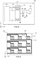
- the figure 3 represents an exemplary embodiment of such tracks 122, 123 connected to a portion of the heating elements 114 of the device 100.
- circuit 120 has an input 121 connected to the ground at which a second end of each of the heating elements 114 is connected via a second track 123.
- the first end of each of the heating elements 114 is connected to another input 125 of the circuit 120, which is distinct for each of these first ends of the heating elements 114, via a first track 122.
- the width of the tracks 122, 123 is here greater than the width of the conductive portions forming the coils of the heating elements 114, in order to limit the access resistances relative to the heating elements 114.
- This width of the tracks 122, 123 is for example equal to at about 2 cm or between about 1 cm and 5 cm, while that of the portions forming the heating elements 114 is for example between about 250 microns and 500 microns.
- FIG 4 represents a top view of a portion of the device 100 in which a region 124 of this device 100 comprises these electrical access parts to these elements.
- the electrical connections to these access regions are for example made via portions of anisotropic adhesive comprising silver balls embedded in the glue, on which an electronic control and measuring circuit is reported, for example a flexible printed circuit comprises a flexible substrate (polyimide for example), which comprises solder pads to which the portions of adhesive are connected.
- a flexible printed circuit comprises a flexible substrate (polyimide for example), which comprises solder pads to which the portions of adhesive are connected.
- Other electrical connection techniques are possible, however.
- the figure 5 schematically represents the electric circuit formed by the various elements of the device 100 previously described.
- the electrodes 108 and 110 of all the pixels 102 are formed by electrically conductive layers 109, 111 common to all the pixels 102, the reading made for each pixel 102 corresponds to a reading of the capacitance formed between these layers 109, 111 and therefore corresponds to all the pixels 102.
- the heating of the pixels 102 is controlled individually for each pixel 102, the simultaneous reading of all the pixels 102 makes it possible to know if an element is present or not above the pixel 102 which is heated.
- Such a device 100 therefore does not use any pixel selection transistor.
- the reading circuit of the device 100 comprises a switch 126 enabling, by connecting the reading electrode 108 to ground, to reset the pyroelectric capacitor, and an analog-to-digital converter (ADC) 128, for example of the type delta-sigma, to read the voltage induced by the charges generated in the pyroelectric capacitance.
- ADC analog-to-digital converter
- the time required to read all the pixels is equal to about 54 seconds.
- the device 100 may comprise an amplifier interposed between the pyroelectric capacitor and the CAN 128.
- the device 100 described above in connection with the first embodiment corresponds to a detection device adapted to carry out a detection of a person in a bed.
- the previously described materials and thicknesses of the various elements of the device 100 allow the device 100 to be flexible.
- such a device 100 can also perform a heating function by virtue of the heat generated by the heating elements 114.
- the dimensions of the device 100 may be adapted so that it serves to carry out a detection on the ground, that is to say integrated in the floor covering, or in the form of a carpet.
- the lower electrode 108 forms the reading electrode and the upper electrode 110 is connected to a reference electrical potential such as ground.
- a reference electrical potential such as ground.
- the upper electrode 110 forms the reading electrode and the lower electrode 108 is connected to ground.
- one of the lower and upper electrodes 108 to form the reading electrode, and the other of the lower and upper electrodes 108 to be formed directly by the heating elements 114.
- a full metal layer is disposed on the dielectric layer 112 to form the shield of the device 100.
- the heating elements 114 are formed by portions of resistive material deposited in the form of coils.
- each heating element 114 in the form of a portion of a different shape, for example of square or rectangular shape, from a more resistive material than that serving to produce the conductive tracks 122, 123, such as PDOT: PSS having a resistivity of between about 100 and 500 ⁇ per square, which makes it possible to achieve a resistance of a square having a resistance of about 100 ⁇ .
- Such heating elements are represented on the figure 6 .
- the figure 7 represents a top view of a portion of the device 100 (not all pixels are shown) according to a second embodiment.
- the layer 109 according to this second embodiment is well continuous from an electrical point of view for all the pixels 102, that is to say that the layer 109 is common to all the pixels 102 and forms the lower electrodes 108 of all pixels 102, but is structured, or etched, such that portions of this layer 109 between pixels 102 are removed.
- the layer 109 comprises first portions 129 facing the heating elements 114 and forming the lower electrodes 108, as well as second portions 130 electrically interconnecting the first portions 129.
- the layer 109 also comprises a third portion 132 electrically connecting the layer 109 to the circuit 120.
- This second embodiment has the advantage of reducing the value of the overall pyroelectric capacitance formed by the pixels 102, and therefore of increasing the value of the voltage (signal lu) obtained at the terminals of the pixels 102.
- each of the first portions 129 forms a square area equal to about 40 mm ⁇ 40 mm
- the total area of the lower 36 electrodes 108 formed by the first portions 129 is equal to about 57.10 -3 m 2 .
- the total capacity of the pixels 102 according to this example of the second embodiment is then equal to about 2.10 -6 F.
- the voltage obtained at the terminals of the capacitance formed by the pixels 102 is in this case of the order of 1 millivolt.
- the figure 7 represents only one possible structuring among many others of the layer 109 forming the lower electrodes 108 of the pixels 102.
- the addressing of the heating elements 114 is carried out using a dedicated electrically conductive track 122 for each of the heating elements 114.
- each conductive track 122 supplies several heating elements 114 per line and / or column and arranging a diode upstream of each heating element 114 (the diode serving to prevent current flow in various interfering paths).
- the diode serving to prevent current flow in various interfering paths.
- This variant can be advantageous when the number of heating elements 114 is large, for example greater than about 50 or 64 (for example, the addressing of 64 heating elements arranged in an 8 ⁇ 8 matrix can be achieved using 8 conductive tracks each connected to one of the 8 lines of heating elements, as well as 8 conductive tracks each connected to one of the 8 columns of heating elements).
- the production of additional resistors and diodes involves the implementation of additional steps that impact the cost of producing the device 100.
- holes 134 through all the layers of the stack of the device 100.
- These holes 134 make it possible in particular to make the device 100 more permeable, thus adding comfort of use for example when the device 100 corresponds to a person detection device for use in a bed.
- the provision of such holes 134 also has the advantage of improving the detection sensitivity of the device 100 because the total pyroelectric capacitance formed by the pixels 102 is reduced (due to the reduction in the area of the layers 109, 111 and 113 of this capacity generated by the formation of the holes 134), and the reading voltage obtained at The limits of this capacity are therefore greater for the same amount of loads generated in the capacity.
- the reading of the pixels 102 is not carried out individually, but by group of pixels 102.
- the heating elements 114 of a these groups of pixels 102 are lit at the same time. This can be used to increase the sensitivity (in terms of voltage level obtained) of the device 100 because the read signal obtained will be larger, but at the expense of the resolution of the device 100 which is reduced.
- the device 100 it is possible to use one of the pixels 102 of the device 100 as a reference, for example one of the pixels 102 arranged in the corners of the matrix of pixels 102. For this, a predetermined thermal load is disposed on this reference pixel. The measurement made for each of the other pixels 102 can then be seen as a differential measurement with respect to this reference pixel, which makes it possible to improve the sensitivity of the device 100.
- this reference pixel it is it is possible to subtract an arbitrary value in tension corresponding to a certain percentage (for example 75%) of the maximum tension obtained for a pixel 102 in contact with air.
- the conductive layer used for producing the heating elements 114 may be used to also form additional electrical resistances not used for the detection carried out by the device 100 but used solely for heating .
- the device 100 may in this case include a thermostat for adjusting this heating, and a thermometer for detecting the absolute temperature of the device 100 because the detection performed corresponds to a detection of a temperature change.
- the device 100 may further comprise an electronic processing circuit capable of constructing a global image obtained from the measurements made at each of the pixels 102.
- This electronic processing circuit may also be able to compare this image. to several images stored in a database.
- the electronic processing circuit may also be able to display an image of the detection performed.
- devices 100 as described above can be arranged side by side, for example on the same substrate, and be electrically connected in parallel with each other.
- the device realizes the detection of a thermal pattern, that is to say the shape of a thermal mass on the device, thanks to the detections made at the different pixels of the device.
- This device may, however, serve to detect not the motive of the thermal mass, but to detect only the presence of this thermal mass on or near the device, for example through a fabric or a coating.
Landscapes
- General Physics & Mathematics (AREA)
- Physics & Mathematics (AREA)
- Engineering & Computer Science (AREA)
- Theoretical Computer Science (AREA)
- Multimedia (AREA)
- Health & Medical Sciences (AREA)
- Emergency Management (AREA)
- Business, Economics & Management (AREA)
- Gerontology & Geriatric Medicine (AREA)
- General Health & Medical Sciences (AREA)
- Spectroscopy & Molecular Physics (AREA)
- Power Engineering (AREA)
- Psychiatry (AREA)
- Psychology (AREA)
- Social Psychology (AREA)
- Photometry And Measurement Of Optical Pulse Characteristics (AREA)
- Radiation Pyrometers (AREA)
Abstract
Dispositif (100) de détection thermique actif comportant plusieurs pixels (102), chaque pixel comprenant : - une capacité pyroélectrique formée par une portion de matériau pyroélectrique disposée entre une électrode inférieure et une électrode supérieure, dans laquelle une première des électrodes inférieure et supérieure correspond à une électrode de lecture du pixel, et - un élément chauffant (114) associé uniquement à ce pixel et apte à chauffer la portion de matériau pyroélectrique de la capacité pyroélectrique dudit pixel indépendamment des autres éléments chauffants associés aux autres pixels lors d'une mesure thermique par la capacité pyroélectrique dudit pixel, dans lequel le dispositif comporte en outre au moins un circuit de lecture auquel les électrodes de lecture sont reliées, et dans lequel les électrodes de lecture sont formées par une première couche électriquement conductrice commune à tous les pixels de la matrice et en contact avec les portions de matériau pyroélectrique des pixels.An active thermal sensing device (100) having a plurality of pixels (102), each pixel comprising: a pyroelectric capacitance formed by a portion of pyroelectric material disposed between a lower electrode and an upper electrode, in which a first of the lower and upper electrodes corresponds to a reading electrode of the pixel, and a heating element (114) associated solely with this pixel and able to heat the pyroelectric material portion of the pyroelectric capacitance of said pixel independently of the other heating elements associated with the other pixels during a thermal measurement by the pyroelectric capacitance of said pixel, wherein the device further comprises at least one read circuit to which the read electrodes are connected, and wherein the read electrodes are formed by a first electrically conductive layer common to all the pixels of the die and in contact with the portions of pyroelectric material of the pixels.
Description
L'invention porte sur un dispositif de détection thermique actif à capacités pyroélectriques dont la structure est adaptée pour des pixels de grande taille. L'invention s'applique notamment à la réalisation d'un dispositif de détection d'une masse thermique importante, par exemple d'un être humain ou d'un animal, et utilisé par exemple pour détecter la présence et/ou les mouvements et/ou la position d'une personne dans un lit, ou bien disposé sur ou dans le sol afin de détecter la présence et/ou les mouvements et/ou la position d'une personne sur ce sol, par exemple pour détecter une chute de cette personne.The invention relates to an active thermal detection device with pyroelectric capacitors whose structure is adapted for large pixels. The invention applies in particular to the production of a device for detecting a large thermal mass, for example of a human being or of an animal, and used, for example, to detect the presence and / or movements and / or the position of a person in a bed, or placed on or in the ground to detect the presence and / or movements and / or position of a person on that ground, for example to detect a fall of that person.
Plusieurs technologies existent pour détecter la présence d'une personne dans un lit. Il est par exemple possible de réaliser une telle détection par un dispositif de détection piézorésistif disposé sous un matelas et comportant des moyens de détection piézorésistifs détectant la présence d'une personne grâce à la pression appliquée par cette personne sur le dispositif.Several technologies exist to detect the presence of a person in a bed. It is for example possible to perform such detection by a piezoresistive detection device disposed under a mattress and comprising piezoresistive detection means detecting the presence of a person thanks to the pressure applied by this person on the device.
Des technologies similaires peuvent être utilisées pour réaliser un dispositif de détection au sol, comme cela par exemple décrit dans le document
Le document
Les inconvénients de ces technologies sont notamment :
- la perte de signal lorsque la pression ne varie plus ou que l'équilibre thermique est atteint dans le cas de l'effet piézoélectrique/pyroélectrique, ce qui arrive lorsque la personne ne bouge plus ou que la température de l'objet en contact avec le dispositif de détection est la même que la température du dispositif;
- que les échanges de chaleur ne dépendent pas de la pression appliquée au premier ordre, ce qui rend le dispositif plus sensible qu'une détection piézorésistive pure.
- the loss of signal when the pressure no longer varies or the thermal equilibrium is reached in the case of the piezoelectric / pyroelectric effect, which happens when the person does not move or the temperature of the object in contact with the detection device is the same as the temperature of the device;
- heat exchanges do not depend on first-order pressure, which makes the device more sensitive than pure piezoresistive detection.
Dans un autre domaine technique qui correspond à celui des capteurs d'empreintes digitales, d'autres technologies de détection sont mises en oeuvre, dont la détection thermique active. Dans de tels capteurs, par exemple ceux décrits dans les documents
Au premier ordre, un tel capteur permet de mesurer la capacité calorifique, également appelée chaleur massique ou capacité thermique massique, d'un élément en contact avec le capteur. Les mesures obtenues dépendent également de la conductivité thermique entre le capteur et la partie de l'élément (crête ou vallée dans le cas d'une empreinte digitale) en présence.In the first order, such a sensor can measure the heat capacity, also called specific heat or specific heat capacity, of an element in contact with the sensor. The measurements obtained also depend on the thermal conductivity between the sensor and the part of the element (peak or valley in the case of a fingerprint) in the presence.
Pour former un capteur thermique actif, les pixels de ce capteur sont couplés à des éléments chauffants utilisant généralement l'effet Joule qui dissipe de la chaleur depuis un élément résistif qui est parcouru par un courant. Un des niveaux de l'empilement technologique formant les pixels est avantageusement utilisé pour former ces éléments chauffants. Par exemple, il possible d'utiliser un des niveaux électriquement conducteurs servant à réaliser les transistors et les interconnexions du capteur si l'un de ces niveaux comporte un matériau conducteur présentant une résistivité adéquate et sur lequel il suffit d'appliquer une des tensions déjà disponibles, par exemple la tension d'alimentation du capteur, pour générer un chauffage par effet Joule. Cela est notamment utilisé lorsque le capteur comporte des transistors de type TFT (« Thin-Film Transistor », ou transistor en couches minces) réalisés sur un substrat de verre ou de plastique.To form an active thermal sensor, the pixels of this sensor are coupled to heating elements generally using the Joule effect which dissipates heat from a resistive element which is traversed by a current. One of the levels of the technological stack forming the pixels is advantageously used to form these heating elements. For example, it is possible to use one of the electrically conductive levels used to make the transistors and the interconnections of the sensor if one of these levels comprises a conductive material having adequate resistivity and on it suffices to apply one of the voltages already available, for example the supply voltage of the sensor, to generate heating by Joule effect. This is especially used when the sensor comprises transistors of the TFT ("Thin-Film Transistor" or thin-film transistor) type produced on a glass or plastic substrate.
Les pixels d'un tel capteur sont disposés en formant une matrice de plusieurs lignes et de plusieurs colonnes de pixels. La lecture des pixels est généralement réalisée ligne par ligne. Les éléments chauffants peuvent alors être également commandés ligne par ligne à l'aide d'un transistor se trouvant en tête de chaque ligne, évitant ainsi l'ajout de transistors de commande dans chacun des pixels. Chaque ligne d'éléments chauffants est par exemple connectée, d'un côté de la matrice de pixels, à la masse, et de l'autre coté au transistor de commande associé à la ligne de pixels et relié à une alimentation adaptée de manière à maîtriser le courant parcourant les éléments chauffants, et donc la puissance thermique injectée par effet Joule dans les pixels par ces éléments chauffants.The pixels of such a sensor are arranged by forming a matrix of several rows and several columns of pixels. The reading of the pixels is generally done line by line. The heating elements can then also be controlled line by line using a transistor at the top of each line, thus avoiding the addition of control transistors in each of the pixels. Each line of heating elements is for example connected, on one side of the pixel matrix, to ground, and on the other side to the control transistor associated with the pixel line and connected to a power supply adapted to control the current flowing through the heating elements, and therefore the thermal power injected by the Joule effect into the pixels by these heating elements.
Pour réaliser une lecture de la variation de charges électriques apparaissant dans la capacité pyroélectrique de chaque pixel d'un capteur thermique actif, chacun des pixels comporte au moins un transistor de sélection, et les transistors de sélection des pixels de chaque colonne de pixels sont reliés à une ligne conductrice elle-même relié à un circuit de lecture. Lors de la lecture d'une ligne de pixels, les transistors de sélection des pixels de cette ligne sont mis à l'état passant, ce qui permet de relier les noeuds actifs des pixels de cette ligne aux circuits de lecture se trouvant en pied de chacune des colonnes de pixels. Les transistors de sélection bloqués des pixels appartenant aux autres lignes de pixels empêchent le déplacement de charges depuis ces autres pixels vers les circuits de lecture. D'autres transistors peuvent également être présents dans chaque pixel, notamment lorsque les pixels sont lus en tension et qu'ils nécessitent la présence d'un transistor de réinitialisation et d'un transistor suiveur de tension, ou que le capteur forme également un capteur optique dans lequel un transistor est présent dans chaque pixel pour relier une photodiode de chaque pixel à un circuit de lecture dédié.To make a reading of the variation of electric charges appearing in the pyroelectric capacitance of each pixel of an active thermal sensor, each of the pixels comprises at least one selection transistor, and the selection transistors of the pixels of each column of pixels are connected. to a conductive line itself connected to a read circuit. When reading a line of pixels, the selection transistors of the pixels of this line are set to the on state, which makes it possible to connect the active nodes of the pixels of this line to the reading circuits at the foot of the line. each of the columns of pixels. Blocked selection transistors of the pixels belonging to the other pixel lines prevent the displacement of charges from these other pixels to the readout circuits. Other transistors may also be present in each pixel, especially when the pixels are read in voltage and they require the presence of a reset transistor and a voltage follower transistor, or the sensor also forms a sensor wherein a transistor is present in each pixel for connecting a photodiode of each pixel to a dedicated read circuit.
Bien que la détection thermique active présente de nombreux avantages par rapport aux autres techniques utilisées pour réaliser par exemple une détection de personne dans un lit ou sur un sol (comme par exemple l'obtention d'un niveau de signal stable indépendant de la température de la personne car c'est principalement sa masse thermique, associée à sa conductivité thermique, qui est impliquée dans un détection thermique active), la structure de ces capteurs d'empreintes digitales n'est pas adaptée pour réaliser une détection de personne en raison des dimensions du dispositif nécessaires à sa réalisation. En effet, un capteur d'empreinte digitale utilise usuellement des pixels ayant un pas égal à environ 50 µm, ce qui n'est pas compatible, et inutile, avec un dispositif de détection ayant des dimensions de l'ordre du mètre. De plus, les épaisseurs des protections de surface d'un dispositif de détection de personne sont de l'ordre d'un ou plusieurs millimètres, ce qui est bien trop important pour un dispositif ayant des pixels réalisés avec un pas égal à environ 50 µm. La présence des transistors au sein des pixels est également contraignante pour réalisation d'un dispositif de détection de personne car la réalisation de ces transistors requière la mise en oeuvre de dépôts supplémentaires de matériaux, ces dépôts étant coûteux.Although the active thermal detection has many advantages over other techniques used to perform for example a person detection in a bed or on a floor (such as obtaining a stable signal level independent of the temperature of the person because it is mainly its thermal mass, associated with its thermal conductivity, which is involved in an active thermal detection), the structure of these fingerprint sensors is not suitable for realizing a person detection because of dimensions of the device necessary for its realization. Indeed, a fingerprint sensor usually uses pixels having a pitch equal to about 50 microns, which is not compatible and unnecessary, with a detection device having dimensions of the order of one meter. In addition, the thicknesses of the surface protections of a person detection device are of the order of one or several millimeters, which is much too important for a device having pixels made with a pitch equal to about 50 μm. . The presence of the transistors within the pixels is also constraining for the realization of a person detection device because the realization of these transistors requires the implementation of additional deposits of materials, these deposits being expensive.
Un but de la présente invention est de proposer un dispositif de détection thermique actif, c'est-à-dire comportant des éléments chauffant les pixels, à capacités pyroélectriques, qui est adapté pour être réalisé avec des pixels de grande taille, apportant ainsi les avantages de la détection thermique active à un dispositif par exemple adapté à la détection d'une personne ou d'un animal lorsque celle-ci ou celui-ci se trouve sur ce dispositif, et qui ne nécessite pas la présence de transistors au sein des pixels.An object of the present invention is to provide an active thermal detection device, that is to say having pixels heating elements, pyroelectric capacitors, which is adapted to be made with pixels of large size, thereby providing the advantages of the active thermal detection device for example adapted to the detection of a person or an animal when the latter or it is on this device, and which does not require the presence of transistors within the pixels.
Pour cela, l'invention propose un dispositif de détection thermique actif comportant plusieurs pixels, chaque pixel comprenant au moins :
- une capacité pyroélectrique formée par au moins une portion de matériau pyroélectrique disposée entre une électrode inférieure et une électrode supérieure, dans laquelle une première des électrodes inférieure et supérieure correspond à une électrode de lecture du pixel, et
- un élément chauffant associé uniquement à ce pixel et apte à chauffer la portion de matériau pyroélectrique de la capacité pyroélectrique dudit pixel indépendamment des autres éléments chauffants associés aux autres pixels lors d'une mesure thermique par la capacité pyroélectrique dudit pixel,
- a pyroelectric capacitance formed by at least a portion of pyroelectric material disposed between a lower electrode and an electrode upper, in which a first of the lower and upper electrodes corresponds to a reading electrode of the pixel, and
- a heating element associated solely with this pixel and able to heat the pyroelectric material portion of the pyroelectric capacitance of said pixel independently of the other heating elements associated with the other pixels during a thermal measurement by the pyroelectric capacitance of said pixel,
Dans ce dispositif, chaque élément chauffant est apte à être commandé individuellement, c'est-à-dire indépendamment des éléments chauffants associés aux autres pixels.In this device, each heating element is able to be controlled individually, that is to say independently of the heating elements associated with the other pixels.
La mise en oeuvre d'une détection thermique active a pour avantage, par rapport à une détection thermique passive, de détecter la présence d'une masse thermique et non uniquement un changement thermique comme c'est le cas pour une détection thermique passive, c'est-à-dire sans moyen de chauffage.The implementation of active thermal detection has the advantage, compared to a passive thermal detection, of detecting the presence of a thermal mass and not only a thermal change as is the case for passive thermal detection, c i.e. without heating means.
Des pixels de grande taille correspondent par exemple à des pixels de dimensions comprises entre environ 1 cm et 10 cm de côté, et/ou réalisés avec un pas par exemple de l'ordre de 10 cm ou compris entre environ 5 cm et 50 cm.Large pixels correspond for example to pixels of dimensions of between about 1 cm and 10 cm side, and / or made with a pitch for example of the order of 10 cm or between about 5 cm and 50 cm.
Dans ce dispositif, les électrodes de lecture sont formées par une première couche électriquement conductrice commune à tous les pixels de la matrice et en contact avec les portions de matériau pyroélectrique des pixels de la matrice. Cette caractéristique est possible grâce au fait que les éléments chauffants sont adressables individuellement. L'électronique de lecture utilisée avec un tel dispositif peut donc comporter une seule entrée, simplifiant donc grandement sa réalisation et la rendant compatible avec les applications envisagées pour des pixels de grande taille.In this device, the reading electrodes are formed by a first electrically conductive layer common to all the pixels of the matrix and in contact with the pyroelectric material portions of the pixels of the matrix. This feature is possible because the heating elements are individually addressable. The reading electronics used with such a device can therefore comprise a single input, thus greatly simplifying its implementation and making it compatible with the applications envisaged for large pixels.
La combinaison des différentes caractéristiques de ce dispositif rend possible la réalisation de pixels de grande taille adaptés pour un dispositif servant à la détection d'une masse thermique ayant une surface importante, c'est-à-dire relativement étendue.The combination of the different characteristics of this device makes it possible to produce large pixels suitable for a device for the detection of a thermal mass having a large surface, that is to say relatively large.
Un autre avantage lié au fait que les éléments chauffants sont adressables individuellement est que la résolution du dispositif peut aisément être modifiée en chauffant plusieurs pixels simultanément.Another advantage related to the fact that the heaters are individually addressable is that the resolution of the device can easily be changed by heating several pixels simultaneously.
De manière avantageuse, un tel dispositif peut être utilisé en tant que détecteur de présence d'une personne, par exemple dans un lit. Dans ce cas, le dispositif est réalisé sous la forme d'une alèze destinée à être disposée entre le matelas et un drap recouvrant le matelas et permettant de détecter la présence ou non d'une personne, voire sa position dans le lit.Advantageously, such a device can be used as a presence detector of a person, for example in a bed. In this case, the device is made in the form of a web to be arranged between the mattress and a sheet covering the mattress and for detecting the presence or absence of a person, or its position in the bed.
Un tel dispositif peut être également disposé sur ou dans un sol, par exemple sous un parquet, afin de détecter la présence et/ou les mouvements d'une personne sur ce sol, par exemple une chute.Such a device can also be placed on or in a floor, for example under a floor, to detect the presence and / or movements of a person on the floor, for example a fall.
Un tel dispositif peut également être utilisé pour détecter une présence d'une personne sur un siège, le dispositif pouvant dans ce cas être disposé sous le tissu du siège.Such a device can also be used to detect a presence of a person on a seat, the device can in this case be arranged under the seat fabric.
Un tel dispositif peut également être disposé sur ou dans un volant (ou plus généralement tout moyen de guidage) d'un véhicule pour détecter qu'une personne tient bien ce volant.Such a device can also be placed on or in a steering wheel (or more generally any guiding means) of a vehicle to detect that a person holds the steering wheel.
Un tel dispositif peut également être utilisé pour réaliser une détection d'eau, de glace ou de neige sur un sol, un toit, etc.Such a device can also be used to detect water, ice or snow on a floor, a roof, etc.
Un tel dispositif peut également être utilisé pour compter un nombre de personnes présentes sur un sol.Such a device can also be used to count a number of people on a floor.
Ce capteur correspond à un capteur actif (car comprenant des pixels chauffés) réalisé avec un ensemble de pixels passifs, c'est-à-dire sans transistors présents au sein des pixels. Ainsi, la réalisation de ce capteur n'est pas limitée par la technologie nécessaire à la réalisation de transistors au sein des pixels, et peut être réalisé en technologie imprimée, par exemple sur un substrat souple.This sensor corresponds to an active sensor (because comprising heated pixels) made with a set of passive pixels, that is to say without transistors present within the pixels. Thus, the realization of this sensor is not limited by the technology necessary for producing transistors within the pixels, and can be achieved in printed technology, for example on a flexible substrate.
Sans transistor au sein des pixels, la fabrication des pixels est simplifiée et se résume à la capacité de réaliser les éléments chauffants et les éléments de connexion de ces éléments chauffants à la résolution souhaitée. Ceci devient possible avec des procédés moins onéreux que la lithographie sur semi-conducteur, tels que les dépôts par impression. Les différentes portions conductrices formant les éléments des pixels du capteur peuvent être réalisées avec des encres conductrices suffisamment stables pour ne pas nécessiter d'encapsulation très performante. La réalisation du capteur est envisageable par impression, par exemple sur des substrats plastiques simples (films PET).Without a transistor within the pixels, pixel fabrication is simplified and boils down to the ability to achieve the heating elements and connection elements of these heating elements at the desired resolution. This becomes possible with less expensive processes than semiconductor lithography, such as deposits by printing. The different conductive portions forming the elements of the pixels of the sensor can be made with conductive inks sufficiently stable not to require high performance encapsulation. The realization of the sensor is possible by printing, for example on simple plastic substrates (PET films).
Un tel capteur a également pour avantage de réduire le nombre de signaux nécessaires à son pilotage du fait que la sélection du pixel lu est réalisée par l'intermédiaire du chauffage de ce pixel.Such a sensor also has the advantage of reducing the number of signals necessary for its control because the selection of the read pixel is performed via the heating of this pixel.
Le capteur comporte en outre un circuit de lecture auquel les électrodes de lecture sont reliées.The sensor further comprises a read circuit to which the reading electrodes are connected.
Les pixels peuvent former ensemble une surface de détection ayant une largeur comprise entre environ 0,5 m et 2 m et une longueur comprise entre environ 1 m et 10 m, ou encore une surface de détection comprise entre environ 0,5 m2 et 10 m2, et/ou chaque pixel peut former une surface de détection ayant des côtés chacun de dimension comprise entre environ 1 cm et 10 cm, ou une surface de détection comprise entre environ 1 cm2 et 100 cm2, et/ou le dispositif peut comporter un nombre de pixels compris entre environ 25 et 250.The pixels may together form a detection surface having a width of between about 0.5 m and 2 m and a length of between about 1 m and 10 m, or a detection surface of between about 0.5 m 2 and 10 m. m 2 , and / or each pixel can form a detection surface having sides each of dimension between about 1 cm and 10 cm, or a detection surface of between about 1 cm 2 and 100 cm 2 , and / or the device may have a number of pixels between about 25 and 250.
Une deuxième des électrodes inférieure et supérieure de chaque pixel peut être formée par une deuxième couche électriquement conductrice commune à tous les pixels et apte à être reliée électriquement à un potentiel électrique de référence. Dans cette configuration, une seule capacité pyroélectrique est commune à tous les pixels de la matrice, simplifiant ainsi la réalisation du dispositif.A second of the lower and upper electrodes of each pixel may be formed by a second electrically conductive layer common to all the pixels and adapted to be electrically connected to an electrical reference potential. In this configuration, a single pyroelectric capacitance is common to all the pixels of the matrix, thus simplifying the realization of the device.
Dans ce cas, la deuxième couche électriquement conductrice peut être disposée entre les éléments chauffants et les électrodes de lecture. Dans cette configuration, la deuxième couche électriquement conductrice forme à la fois les électrodes supérieures des pixels et une couche de blindage électromagnétique du dispositif.In this case, the second electrically conductive layer may be disposed between the heating elements and the reading electrodes. In this configuration, the second electrically conductive layer forms both the upper electrodes of the pixels and an electromagnetic shielding layer of the device.
Le dispositif peut comporter en outre une couche diélectrique recouvrant les électrodes supérieures des pixels et sur laquelle les éléments chauffants sont disposés.The device may further comprise a dielectric layer covering the upper electrodes of the pixels and on which the heating elements are arranged.
Chaque élément chauffant peut comporter une ou plusieurs portions de matériau formant un élément résistif disposé à l'aplomb d'une partie de la capacité pyroélectrique du pixel et dont des première et deuxième extrémités sont reliées électriquement, par l'intermédiaire de premières et deuxièmes pistes électriquement conductrices, à un circuit de commande électronique apte à faire circuler un courant électrique de chauffage dans chaque élément résistif individuellement tel qu'il chauffe par effet Joule la capacité pyroélectrique du pixel.Each heating element may comprise one or more portions of material forming a resistive element disposed vertically above a portion of the pyroelectric capacitance of the pixel and of which first and second ends are electrically connected, via first and second tracks. electrically conductive, to an electronic control circuit capable of circulating an electric heating current in each resistive element individually as it heats by Joule effect the pyroelectric capacitance of the pixel.
Dans ce cas, chaque élément résistif peut comporter une ou plusieurs portions de matériau résistif de section inférieure à celle des premières et deuxièmes pistes conductrices, et par exemple disposées selon un motif de serpentin, et/ou le matériau de la ou les portions formant chaque élément résistif a une résistivité supérieure à un matériau des premières et deuxièmes pistes électriquement conductrices.In this case, each resistive element may comprise one or more portions of resistive material of smaller section than the first and second conductive tracks, and for example arranged in a serpentine pattern, and / or the material of the portion or portions forming each resistive element has a higher resistivity than a material of the first and second electrically conductive tracks.
La première extrémité de chaque élément résistif peut être reliée électriquement au circuit de commande électronique par l'intermédiaire d'une des premières pistes électriquement conductrices distincte des autres premières pistes électriquement conductrices reliant électriquement les premières extrémités des autres éléments résistifs au circuit de commande électronique, et/ou les deuxièmes extrémités des éléments résistifs des pixels peuvent être reliées électriquement au circuit de commande électronique par l'intermédiaire des deuxièmes pistes électriquement conductrices qui sont reliées électriquement entre elles. Les deuxièmes pistes électriquement conductrices peuvent être reliées à la masse.The first end of each resistive element can be electrically connected to the electronic control circuit via one of the first electrically conductive tracks distinct from the other first electrically conductive tracks electrically connecting the first ends of the other resistive elements to the electronic control circuit, and / or the second ends of the pixel resistive elements can be electrically connected to the electronic control circuit via the second electrically conductive tracks which are electrically connected to each other. The second electrically conductive tracks can be connected to ground.
Des parties des couches formant les électrodes inférieures et supérieures des pixels et des parties des premières et deuxièmes pistes électriquement conductrices peuvent ne pas être recouvertes par d'autres matériaux et peuvent former des accès électriques aux électrodes inférieures et supérieures et aux éléments chauffants.Parts of the layers forming the lower and upper electrodes of the pixels and portions of the first and second electrically conductive tracks may not be covered by other materials and may form electrical accesses to the lower and upper electrodes and the heating elements.
La première couche électriquement conductrice peut être gravée telle qu'elle comporte des premières portions localisées sous les éléments chauffants et formant les électrodes de lecture des pixels, et des deuxièmes portions reliant électriquement entre elles les premières portions. Cette configuration permet de réduire la valeur de la capacité pyroélectrique des pixels.The first electrically conductive layer may be etched as it comprises first portions located under the heating elements and forming the reading electrodes of the pixels, and the second portions connecting electrically between them the first portions. This configuration makes it possible to reduce the value of the pyroelectric capacitance of the pixels.
Le dispositif peut comporter en outre des trous traversant le dispositif. Ces trous confèrent une perméabilité à l'humidité du dispositif et réduit également la valeur de la capacité pyroélectrique des pixels.The device may further comprise holes passing through the device. These holes impart permeability to the humidity of the device and also reduce the value of the pyroelectric capacitance of the pixels.
Le matériau pyroélectrique peut être du PVDF ou du P(VDF-TrFE), et/ou les pixels peuvent être disposés les uns à côté des autres en formant une matrice de plusieurs lignes et colonnes.The pyroelectric material may be PVDF or P (VDF-TrFE), and / or the pixels may be arranged next to one another forming a matrix of several rows and columns.
L'invention concerne également un procédé de réalisation d'un dispositif de détection thermique actif comportant plusieurs pixels, le procédé comportant au moins la mise en oeuvre des étapes suivantes :
- réalisation, pour chaque pixel, d'au moins une capacité pyroélectrique formée par au moins une portion de matériau pyroélectrique disposée entre une électrode inférieure et une électrode supérieure, dans laquelle une première des électrodes inférieure et supérieure correspond à une électrode de lecture du pixel ;
- réalisation, pour chaque pixel, d'au moins un élément chauffant associé uniquement à ce pixel et apte à chauffer la portion de matériau pyroélectrique de la capacité pyroélectrique dudit pixel indépendamment des autres éléments chauffants associés aux autres pixels lors d'une mesure thermique par la capacité pyroélectrique dudit pixel,
- producing, for each pixel, at least one pyroelectric capacitance formed by at least one portion of pyroelectric material disposed between a lower electrode and an upper electrode, wherein a first of the lower and upper electrodes corresponds to a reading electrode of the pixel;
- making, for each pixel, at least one heating element associated only with this pixel and able to heat the pyroelectric material portion of the pyroelectric capacitance of said pixel independently of the other heating elements associated with the other pixels during a thermal measurement by the pyroelectric capacitance of said pixel,
La réalisation des électrodes inférieures des pixels et/ou des électrodes supérieures des pixels et/ou des éléments chauffants des pixels peut comporter la mise en oeuvre d'au moins un dépôt par impression d'au moins un matériau électriquement conducteur. Le dépôt par impression a pour avantage de fortement réduire le coût lié à la réalisation du dispositif.The realization of the lower electrodes of the pixels and / or the upper electrodes of the pixels and / or the pixel heating elements may comprise the implementation of at least one deposition by printing of at least one electrically conductive material. The deposit by printing has the advantage of greatly reducing the cost associated with the production of the device.
La réalisation de la capacité pyroélectrique de chaque pixel peut comporter la mise en oeuvre d'une gravure de la première couche électriquement conductrice telle que des portions restantes de la première couche électriquement conductrice forment des premières portions localisées sous les éléments chauffants et formant les électrodes de lecture des pixels, et des deuxièmes portions reliant électriquement entre elles les premières portions.The realization of the pyroelectric capacitance of each pixel can comprise the implementation of an etching of the first layer electrically conductive such that remaining portions of the first electrically conductive layer form first portions located under the heating elements and forming the reading electrodes of the pixels, and second portions electrically interconnecting the first portions.
Le procédé comporte également la réalisation d'un circuit de lecture auquel les électrodes de lecture sont reliées.The method also comprises producing a reading circuit to which the reading electrodes are connected.
La présente invention sera mieux comprise à la lecture de la description d'exemples de réalisation donnés à titre purement indicatif et nullement limitatif en faisant référence aux dessins annexés sur lesquels :
- la
figure 1 représente une vue en coupe d'un pixel d'un dispositif de détection thermique actif, objet de la présente invention ; - les
figures 2 à 4 représentent des vues de dessus d'une partie d'un dispositif de détection thermique actif, objet de la présente invention, selon un premier mode de réalisation ; - la
figure 5 représente schématiquement le circuit électrique formé par les différents éléments du dispositif de détection thermique actif, objet de la présente invention, selon le premier mode de réalisation ; - la
figure 6 représente schématiquement des éléments chauffants d'un dispositif de détection thermique actif, objet de la présente invention, selon une variante de réalisation ; - la
figure 7 représente une vue de dessus d'une partie d'un dispositif de détection thermique actif, objet de la présente invention, selon un deuxième mode de réalisation ; - la
figure 8 représente une vue de dessus d'une partie d'un dispositif de détection thermique actif, objet de la présente invention, selon une variante du premier mode de réalisation.
- the
figure 1 represents a sectional view of a pixel of an active thermal detection device, object of the present invention; - the
Figures 2 to 4 represent top views of a portion of an active thermal detection device, object of the present invention, according to a first embodiment; - the
figure 5 schematically represents the electric circuit formed by the different elements of the active thermal detection device, object of the present invention, according to the first embodiment; - the
figure 6 schematically represents heating elements of an active thermal detection device, object of the present invention, according to an alternative embodiment; - the
figure 7 represents a view from above of a portion of an active thermal detection device, object of the present invention, according to a second embodiment; - the
figure 8 represents a top view of a portion of an active thermal detection device object of the present invention, according to a variant of the first embodiment.
Des parties identiques, similaires ou équivalentes des différentes figures décrites ci-après portent les mêmes références numériques de façon à faciliter le passage d'une figure à l'autre.Identical, similar or equivalent parts of the different figures described below bear the same numerical references so as to facilitate the passage from one figure to another.
Les différentes parties représentées sur les figures ne le sont pas nécessairement selon une échelle uniforme, pour rendre les figures plus lisibles.The different parts shown in the figures are not necessarily in a uniform scale, to make the figures more readable.
Les différentes possibilités (variantes et modes de réalisation) doivent être comprises comme n'étant pas exclusives les unes des autres et peuvent se combiner entre elles.The different possibilities (variants and embodiments) must be understood as not being exclusive of each other and can be combined with one another.
On se réfère tout d'abord à la
Le pixel 102 est réalisé sur un substrat 104 correspondant par exemple à un substrat souple, par exemple à base de polyimide ou de PEN (polyéthylène naphtalate) ou de PET (polyéthylène téréphtalate), sur lequel les éléments électriques du capteur 100 sont réalisés par technologie imprimée (par exemples via une réalisation avec des têtes d'écriture de type jet d'encre). L'épaisseur du substrat 104 est par exemple égale à environ 125 µm ou plus généralement comprise entre environ 50 µm et 250 µm.The
Les pixels 102 du capteur 100 sont ici disposés en formant une matrice de plusieurs lignes et plusieurs colonnes de pixels 102. Le pas des pixels 102, dans le plan (X,Y) (c'est-à-dire le plan du substrat 104), est par exemple égal à environ 10 cm (pour des pixels de dimension 10 x 10 cm dans le plan (X,Y)), ou compris entre environ 10 cm et 20 cm, ou plus généralement compris entre environ 5 cm et 50 cm.The
Les pixels 102 peuvent être régulièrement répartis sur l'ensemble de la surface de détection du dispositif 100. Toutefois, il est possible de ne pas disposer de pixels 102 au niveau des bords du dispositif 100. De manière générale, il est possible que la répartition des pixels 102 sur l'ensemble de la surface de détection du dispositif 100 ne soit pas uniforme, certaines régions du dispositif 100 pouvant être plus ou moins denses que le reste de la surface du dispositif 100.The
Pour les applications de détection d'une personne, la surface de détection du dispositif (correspondant à la surface dans le plan (X,Y) des différentes figures) est par exemple comprise entre environ 0,5 m x 1 m et 2 m x 2 m. En outre, chaque pixel peut former une surface de détection ayant des côtés de dimension comprise entre environ 1 cm et 10 cm. Enfin, le dispositif 100 peut comporter un nombre de pixels compris entre environ 25 et 250.For the applications of detection of a person, the detection surface of the device (corresponding to the surface in the plane (X, Y) of the different figures) is for example between about 0.5 mx 1 m and 2 mx 2 m . In addition, each pixel may form a detection surface having dimension sides of between about 1 cm and 10 cm. Finally, the
Chacun des pixels 102 du capteur 100 comporte des moyens de mesure, ou de détection, thermique formés par une capacité pyroélectrique. Chaque capacité pyroélectrique comporte une portion 106 de matériau pyroélectrique disposée entre une électrode inférieure 108 et une électrode supérieure 110. Le matériau pyroélectrique de la portion 106 est ici un copolymère, avantageusement du P(VDF-TrFE) ou du PVDF. En variante, le matériau pyroélectrique de la portion 106 peut être de l'AIN ou du PZT, ou tout autre matériau pyroélectrique adapté pour former une capacité pyroélectrique. L'épaisseur de la portion 106 est par exemple égale à environ 3 µm, et par exemple comprise entre environ 2 et 10 µm.Each of the
Les électrodes 108, 110 comportent chacune au moins un matériau électriquement conducteur, par exemple un matériau métallique tel que de l'argent, du cuivre, du carbone ou encore du PEDOT (poly(3,4-éthylènedioxythiophène) sous la forme d'encre déposée par impression. L'épaisseur de chacune des électrodes 108, 110 est par exemple égale à environ 5 µm ou comprise entre environ µm et 10 µm.The
Les électrodes inférieures 108 sont formées par une première couche électriquement conductrice 109, ici métallique, commune à tous les pixels 102 de la matrice 100. De même, les électrodes supérieures 110 sont formées par une deuxième couche électriquement conductrice 111, ici métallique, commune à tous les pixels 102 de la matrice 100. Les portions 106 de matériau pyroélectrique de l'ensemble des pixels de la matrice du capteur 100 sont également réalisées sous la forme d'une seule couche de matériau pyroélectrique 113 recouvrant la première couche 109 qui forme les électrodes inférieures 108. La deuxième couche 111 qui forme les électrodes supérieures 110 recouvre cette couche de matériau pyroélectrique 113.The
Dans ce premier mode de réalisation, les première et deuxième couches 109, 111 ainsi que la couche de matériau pyroélectrique 113 sont donc continues, c'est-à-dire ne sont pas interrompues entre les pixels 102.In this first embodiment, the first and
La deuxième couche 111 forme un blindage électromagnétique au sein de l'empilement de couches du dispositif 100, évitant ainsi la récupération de bruit électromagnétique (par exemple du bruit à 50 Hz provenant du secteur) dans les mesures réalisées. Cette deuxième couche 111 permet également de protéger le dispositif 100 vis-à-vis des décharges électrostatiques (ESD).The
La deuxième couche 111 est recouverte par une couche diélectrique 112 d'épaisseur par exemple égale à environ 3 µm ou comprise entre environ 3 µm et 5 µm, et sur laquelle des éléments chauffants 114 des pixels 102 sont réalisés. Chacun des éléments chauffants 114 forme un élément métallique résistif (résistance électrique par exemple comprise entre environ 10 Ω et 100 Ω) associé à un pixel 102 et qui permet de chauffer ce pixel 102 indépendamment des éléments chauffants 114 associés aux autres pixels 102. Les éléments chauffants 114 permettent, lors d'une détection mise en oeuvre par le dispositif 100, de dissiper une certaine quantité de chaleur dans les pixels 102, et notamment dans le matériau pyroélectrique de la couche 113. Dans chaque pixel 102, le chauffage de la portion 106 de matériau pyroélectrique est obtenu en faisant circuler un courant dans l'élément chauffant 114 formant la résistance de chauffage de chacun des pixels 102. Les éléments chauffants 114 sont par exemple réalisés par un dépôt d'une encre métallique, comprenant par exemple de l'argent, déposée par impression avec une épaisseur égale à environ 5 µm ou comprise entre environ 1 µm et 10 µm.The
Les éléments chauffants 114 ainsi que les parties de la couche diélectrique 112 sur lesquelles les éléments chauffants 114 ne sont pas présents sont recouverts par une couche de protection 116, correspondant par exemple à une couche laminée de PET ou de tout autre matériau adapté à la réalisation de cette couche. L'épaisseur de la couche de protection 116 peut être comprise entre quelques microns (par exemple 5 µm) et environ 100 µm, par exemple égale à environ 50 µm, ou bien être plus importante (par exemple de l'ordre de 300 µm ou plus). Dans l'exemple de réalisation décrit ici, l'épaisseur de la couche de protection 116 est égale à environ 25 µm. De manière alternative, la couche de protection 116 peut correspondre à une couche de DLC (Diamond Like Carbon) d'épaisseur inférieure à environ 1 µm.The
Une face supérieure 118 de la couche de protection 116 correspond à la surface au-dessus de laquelle la détection thermique est destinée à être réalisée. Par exemple, cette face supérieure 118 forme la surface sur laquelle la présence d'une personne est destinée à être détectée.An
Pour que le PVDF de la portion 106 acquière ses propriétés pyroélectriques (et aussi piézoélectriques), ce matériau est soumis, une fois pour toute la durée de vie de la capacité pyroélectrique, à un champ électrique d'environ 100 volts par micron d'épaisseur de PVDF. Les molécules à l'intérieur du PVDF s'orientent, et restent orientées ainsi, même lorsque le PVDF n'est plus soumis à ce champ électrique. Le PVDF peut être ainsi polarisé en appliquant une tension de polarisation initiale aux bornes des électrodes 108, 110.In order for the PVDF of the
Après cette polarisation initiale, lorsque la portion 106 est soumise à une variation de température ΔT induite par exemple par la présence d'une personne sur le dispositif 100, cette variation de température ΔT provoque l'apparition d'un champ électrique supplémentaire générant des charges ΔQ. entre les électrodes 108, 110 telles que : ![]()
![]()
Le paramètre S correspond à la surface de la portion 106 en regard avec chacun des éléments chauffants. Le paramètre γ correspond au coefficient pyroélectrique du matériau pyroélectrique de la portion 106. Par exemple, le coefficient pyroélectrique γ du PVFD-TrFE est égal à environ 32 µC/m2/K.The parameter S corresponds to the surface of the
La portion 106 et les électrodes 108, 110 formant une capacité de valeur C, les charges ΔQ générées induisent une différence de potentiels électriques ΔV entre les électrodes 108, 110 telle que : ![]()
![]()
Dans le dispositif 100 décrit ici, la capacité pyroélectrique est commune à tous les pixels 102 du dispositif. Ainsi, la distinction entre les pixels lus se fait grâce au fait que les éléments chauffants 114 sont adressables individuellement.In the
Lorsque le potentiel sur l'électrode de lecture (formée par l'une des électrodes 108, 110, et ici de préférence l'électrode inférieure 108, l'autre des électrodes étant reliée à la masse) est fixe (lecture dite « en courant »), les charges générées s'écoulent vers un circuit de lecture en formant un courant intégré en sortie, avec dans ce cas : ![]()
![]()
Le sens du courant obtenu entre les électrodes 108, 110 dépend du sens du champ électrique avec lequel le PVDF de la portion 106 a été initialement polarisé. Dans le cas de certains autres matériaux pyroélectriques tels que le nitrure d'aluminium, ce sens de polarisation initiale dépend de la manière avec laquelle le matériau pyroélectrique a été déposé, de son ordre et de son orientation cristallographique. En outre, le sens du courant obtenu peut varier suivant que la variation de température subie par la capacité pyroélectrique soit positive ou négative.The direction of the current obtained between the
De manière générale, toutes les couches de matériau du dispositif 100 peuvent être déposées par impression.In general, all the material layers of the
La
Le dispositif 100 correspond à un dispositif de détection de personne adapté pour réaliser une détection d'une personne dans un lit. Ainsi, le dispositif 100 est ici destiné à être disposé sur un matelas et sous un drap en matière textile d'une épaisseur par exemple de l'ordre quelques centaines de microns à 1 mm. Le dispositif 100 a ici une longueur « b » égale à environ 190 cm et une largeur « c » égale à environ 90 cm. Ces valeurs peuvent bien entendu différer selon les dimensions souhaitées (plus petites par exemple pour un berceau ou une couveuse).The
Dans ce premier mode de réalisation, les éléments chauffants 114 correspondent à des éléments résistifs comportant chacun, pour un pixel 102, une portion de matériau conducteur résistif disposée selon un motif de serpentin, et donc apte à chauffer par effet Joule la portion de matériau pyroélectrique de ce pixel 102. Chacun des éléments chauffants 114 forme une résistance électrique ici égale à environ 100 Ω, destinée à être alimentée via l'application d'une tension électrique aux bornes, ou extrémités, de chaque élément chauffant 114, la valeur de cette tension électrique étant par exemple comprise entre environ 3 V et 10 V. En réalisant les éléments résistifs avec de l'encre à base d'argent, la largeur de la portion formant le serpentin est par exemple comprise entre environ 250 µm et 500 µm.In this first embodiment, the
La valeur de la tension de chauffage appliquée aux bornes des éléments chauffants 114 est choisie en fonction de la puissance de chauffage désirée, cette puissance étant fonction notamment de la résistivité du matériau des éléments chauffants 114, de l'épaisseur de la portion de matériau pyroélectrique destinée à être chauffée ainsi que de l'épaisseur des différentes couches du dispositif 100, du coefficient pyroélectrique du matériau pyroélectrique, de la sensibilité du circuit de lecture, du niveau de bruit du circuit de lecture et du temps d'intégration. Dans un pixel 102 du dispositif 100 décrit ici, la puissance de chauffage est par exemple de l'ordre de 1 W ou comprise entre environ 100 mW et 2 W.The value of the heating voltage applied across the
En outre, la variation de température du matériau pyroélectrique à obtenir peut être égale à environ 200 mK, avec une différence d'environ 50 mK entre un pixel en contact avec du vide et un pixel en contact avec la personne, après un temps d'intégration d'environ 0,5 s, ou une différence comprise entre environ 5 mK et 100 mK.In addition, the temperature variation of the pyroelectric material to be obtained may be equal to about 200 mK, with a difference of about 50 mK between a pixel in contact with a vacuum and a pixel in contact with the person, after a period of time. integration of about 0.5 s, or a difference of between about 5 mK and 100 mK.
Ainsi, lorsque l'une des deux extrémités d'un des éléments chauffants 114 est reliée à la masse et qu'un potentiel de chauffage Vchauffe est appliqué sur l'autre extrémité de cet élément chauffant 114, un courant s'écoule alors depuis cette autre extrémité jusqu'à celle reliée à la masse, provoquant un échauffement par effet Joule dans cet élément chauffant 114, et échauffant ainsi le matériau pyroélectrique du pixel 102 dont cet élément chauffant 114 fait partie. Par exemple, l'application d'une tension de 10 V aux bornes d'un élément chauffant 114 formant une résistance de 100 Ω provoque une dissipation d'une puissance de 1 W.Thus, when one of the two ends of one of the
Chaque élément chauffant 114 occupe par exemple une surface de section, dans le plan principal de la couche diélectrique 112 (plan (X,Y)), de forme carré dont le côté a pour dimension une valeur appelée « a » par exemple égale à environ 32 mm, ou comprise entre environ 10 mm et 100 mm.Each
De plus, chaque élément chauffant 114 est ici disposé au centre de chaque pixel 102 qui correspond à une surface par exemple carrée et de dimensions égales à environ 20 cm x 20 cm, ou comprises entre environ 5 cm x 5 cm et 50 cm x 50 cm. Dans l'exemple décrit ici, deux éléments chauffants 114 voisins sont par exemple espacés l'un de l'autre d'une distance égale à environ 19 cm.In addition, each
Cette disposition des éléments chauffants 114 aux centres des pixels 102 permet de concentrer le chauffage réalisé dans chaque pixel 102, augmentant ainsi les différences de températures et facilitant ainsi la propagation thermique vers la masse thermique à détecter.This arrangement of the
Dans chaque pixel 102 du dispositif 100, une capacité pyroélectrique est formée par les parties des couches 109, 111 qui sont superposées l'une au-dessus de l'autre ainsi que du matériau pyroélectrique se trouvant entre ces parties des couches 109,111.In each
En outre, les éléments chauffants 114 se trouvant en périphérie de la matrice d'éléments chauffants 114 formée sur la couche diélectrique 112 sont espacés des bords de la couche diélectrique 112 d'une distance d par exemple égale à environ 15 cm.In addition, the
Du fait que chacun des éléments chauffants 114 est destiné à être commandé individuellement, c'est-à-dire indépendamment des autres éléments chauffants 114, chaque élément chauffant 114 comporte ses deux extrémités reliés à un circuit de commande électronique 120 par l'intermédiaire d'une première et d'une deuxième pistes électriquement conductrices 122, 123. La
La largeur des pistes 122, 123 est ici supérieure à la largeur des portions conductrices formant les serpentins des éléments chauffants 114, afin de limiter les résistances d'accès par rapport aux éléments chauffants 114. Cette largeur des pistes 122, 123 est par exemple égale à environ 2 cm ou comprise entre environ 1 cm et 5 cm, tandis que celle des portions formant les éléments chauffants 114 est par exemple comprise entre environ 250 µm et 500 µm.The width of the
Des accès électriques aux couches 109, 111 ainsi qu'aux éléments chauffants 114 sont formés en ne recouvrant pas certaines parties de ces couches 109, 111 et des éléments chauffants 114. La
La
Du fait que les électrodes 108 et 110 de tous les pixels 102 sont formées par des couches électriquement conductrices 109, 111 communes à tous les pixels 102, la lecture réalisée pour chaque pixel 102 correspond à une lecture de la capacité formée entre ces couches 109, 111 et qui correspond donc à tous les pixels 102. Toutefois, étant donné que le chauffage des pixels 102 est commandé individuellement pour chaque pixel 102, la lecture simultanée de tous les pixels 102 permet de savoir si un élément est présent ou non au-dessus du pixel 102 qui est chauffé.Since the
Un tel dispositif 100 ne fait donc appel à aucun transistor de sélection de pixel.Such a
Le circuit de lecture du dispositif 100 comporte un interrupteur 126 permettant, en connectant l'électrode de lecture 108 à la masse, de remettre à zéro la capacité pyroélectrique, ainsi qu'un convertisseur analogique - numérique (CAN) 128, par exemple de type delta-sigma, permettant de lire la tension induite par les charges générées dans la capacité pyroélectrique.The reading circuit of the
La lecture de chaque pixel 102 peut être réalisée de la manière suivante :
- application d'une tension aux bornes de l'élément chauffant 114 du
pixel 102 destiné à être lu ; - remise à zéro de la capacité pyroélectrique en fermant l'interrupteur 126. Cette remise à zéro de la capacité pyroélectrique est réalisée juste après l'application de la tension aux bornes de l'élément chauffant 114 du
pixel 102 pour éviter d'injecter des charges liées à l'augmentation de tension aux bornes de l'élément chauffant 114 ou aux divers appels de courant provoquant du bruit ; - attente du temps d'intégration ζ, par exemple égal à environ 0,5 seconde ;
- lecture de la tension aux bornes de la capacité pyroélectrique avec le
CAN 128 ; - remise à zéro de la capacité pyroélectrique en fermant l'interrupteur 126 ;
- attente d'un temps de refroidissement par exemple au moins égal à deux fois le temps d'intégration ζ.
- applying a voltage across the
heating element 114 of thepixel 102 to be read; - resetting the pyroelectric capacitance by closing the
switch 126. This resetting of the pyroelectric capacitance is performed just after the application of the voltage across theheating element 114 of thepixel 102 to avoid injecting charges. related to the voltage increase across theheating element 114 or to the various current draws causing noise; - waiting for the integration time ζ, for example equal to about 0.5 seconds;
- reading the voltage across the pyroelectric capacitor with
CAN 128; - resetting the pyroelectric capacitance by closing the
switch 126; - waiting for a cooling time for example at least equal to twice the integration time ζ.
Ces opérations sont répétées pour lire chaque pixel. Ainsi, pour réaliser la lecture du dispositif 100 lorsqu'il comporte une matrice de 9 x 4 pixels 102, soit 36 pixels, le temps nécessaire à la lecture de tous les pixels est égal à environ 54 secondes.These operations are repeated to read each pixel. Thus, to perform the reading of the
Afin de réduire le temps de lecture nécessaire à la lecture de la matrice de pixels 102 du dispositif 100, il est possible d'augmenter l'énergie, et donc la puissance, de chauffe des pixels 102 et ainsi réduire la durée pendant laquelle le matériau pyroélectrique des pixels 102 est chauffé.In order to reduce the reading time required for reading the
En variante, le dispositif 100 peut comporter un amplificateur interposé entre la capacité pyroélectrique et le CAN 128.Alternatively, the
Le dispositif 100 décrit ci-dessus en lien avec le premier mode de réalisation correspond à un dispositif de détection adapté pour réaliser une détection d'une personne dans un lit. Les matériaux et épaisseurs précédemment décrits des différents éléments du dispositif 100 permettent au dispositif 100 d'être souple. En outre, un tel dispositif 100 peut également réaliser une fonction de chauffage grâce à la chaleur générée par les éléments chauffants 114.The
En variante, les dimensions du dispositif 100 peuvent être adaptées pour qu'il serve à réaliser une détection au sol, c'est-à-dire intégré dans le revêtement de sol, ou encore sous la forme d'un tapis.As a variant, the dimensions of the
Dans le premier mode de réalisation précédemment décrit, l'électrode inférieure 108 forme l'électrode de lecture et l'électrode supérieure 110 est reliée à un potentiel électrique de référence tel que la masse. En variante, il est possible que l'électrode supérieure 110 forme l'électrode de lecture et que l'électrode inférieure 108 soit reliée à la masse.In the first embodiment previously described, the
Selon une autre variante de réalisation, il est possible que l'une des électrodes inférieure 108 et supérieure 110 forme l'électrode de lecture, et que l'autre des électrodes inférieure 108 et supérieure 110 soit formée directement par les éléments chauffants 114. Dans ce cas, une pleine couche métallique est disposée sur la couche diélectrique 112 pour former le blindage du dispositif 100.According to another variant embodiment, it is possible for one of the lower and
En outre, dans le premier mode de réalisation précédemment décrit, les éléments chauffants 114 sont formés par des portions de matériau résistif déposées sous la forme de serpentins. En variante, il est toutefois possible de réaliser chaque élément chauffant 114 sous la forme d'une portion de forme différente, par exemple de forme carrée ou rectangulaire, à partir d'un matériau plus résistif que celui servant à réaliser les pistes conductrices 122, 123, comme par exemple du PDOT:PSS ayant une résistivité comprise entre environ 100 et 500 Ω par carré, ce qui permet de réaliser une résistance d'un carré ayant une résistance d'environ 100 Ω. De tels éléments chauffants sont représentés sur la
La
Contrairement au premier mode de réalisation dans lequel la couche 109 formant les électrodes inférieures 108 est continue et a une surface sensiblement également à celles des autres couches 113, 111 et 112 du dispositif 100 (hormis au niveau des régions d'accès électrique à ces couches), la couche 109 selon ce deuxième mode de réalisation est bien continue d'un point de vue électrique pour l'ensemble des pixels 102, c'est-à-dire que la couche 109 est commune à tous les pixels 102 et forme les électrodes inférieures 108 de tous les pixels 102, mais est structurée, ou gravée, telle que des parties de cette couche 109 se trouvant entre les pixels 102 soient supprimées. Sur l'exemple de la
Ce deuxième mode de réalisation a pour avantage de réduire la valeur de la capacité pyroélectrique globale formée par les pixels 102, et donc d'augmenter la valeur de la tension (signal lu) obtenue aux bornes des pixels 102.This second embodiment has the advantage of reducing the value of the overall pyroelectric capacitance formed by the
Par exemple, si chacune des premières portions 129 forme un carré de surface égale à environ 40 mm x 40 mm, la surface totale des 36 électrodes inférieures 108 formées par les premières portions 129 est égale à environ 57.10-3 m2. En considérant que la surface totale occupée par les portions 130 et 132 est sensiblement similaire, la surface totale obtenue est environ 17 fois inférieure à celle occupée par la couche 109 non gravée comme dans le premier mode de réalisation (de surface égale à 0,9 m x 1,9 m = 1,7 m2). La capacité totale des pixels 102 selon cet exemple du deuxième mode de réalisation est alors égale à environ 2.10-6 F. La tension obtenue aux bornes de la capacité formée par les pixels 102 est dans ce cas de l'ordre d'1 millivolt.For example, if each of the
La
Dans les modes de réalisation précédemment décrits, l'adressage des éléments chauffants 114 est réalisé en utilisant une piste électriquement conductrice 122 dédiée pour chacun des éléments chauffants 114. En variante, il est possible que l'adressage des éléments chauffants 114 soit réalisé tel que chaque piste conductrice 122 alimente plusieurs éléments chauffants 114 par ligne et/ou par colonne et en disposant en amont de chaque élément chauffant 114 une diode (la diode servant à éviter la circulation du courant dans divers chemins parasites). Ainsi, seul l'élément chauffant 114 se trouvant au croisement de la ligne et de la colonne alimentées chauffe. Cette variante peut être avantageuse lorsque le nombre d'éléments chauffants 114 est important, par exemple supérieur à environ 50 ou 64 (par exemple, l'adressage de 64 éléments chauffants disposés selon une matrice 8 x 8 peut être réalisé en utilisant 8 pistes conductrices chacune reliée à une des 8 lignes d'éléments chauffants, ainsi que de 8 pistes conductrices chacune reliée à une des 8 colonnes d'éléments chauffants). Toutefois, la réalisation des résistances et diodes supplémentaires implique la mise en oeuvre d'étapes supplémentaires qui impactent le coût de réalisation du dispositif 100.In the embodiments described above, the addressing of the
Selon une variante de réalisation représentée sur la
Quel que soit le mode de réalisation et/ou la variante de réalisation du dispositif 100, il est possible que la lecture des pixels 102 ne soit pas réalisée individuellement, mais par groupe de pixels 102. Pour cela, les éléments chauffants 114 d'un de ces groupes de pixels 102 sont allumés en même temps. Cela peut servir à augmenter la sensibilité (en termes de niveau de tension obtenu) du dispositif 100 car le signal de lecture obtenu sera plus important, mais au détriment de la résolution du dispositif 100 qui est réduite.Whatever the embodiment and / or the embodiment variant of the
Quel que soit le mode de réalisation et/ou la variante de réalisation du dispositif 100, il est possible d'utiliser un des pixels 102 du dispositif 100 en tant que référence, par exemple un des pixels 102 disposés dans les coins de la matrice de pixels 102. Pour cela, une charge thermique prédéterminée est disposée sur ce pixel de référence. La mesure réalisée pour chacun des autres pixels 102 peut alors être vue comme une mesure différentielle vis-à-vis de ce pixel de référence, ce qui permet d'améliorer la sensibilité du dispositif 100. En variante de ce pixel de référence, il est possible de soustraire une valeur arbitraire en tension, correspondant à un certain pourcentage, (par exemple 75 %) de la tension maximale obtenue pour un pixel 102 en contact avec de l'air. Selon une autre variante, il est possible d'ajuster la puissance injectée de manière à atteindre la tension maximale du CAN 128, puis de considérer une partie de cette tension maximale, par exemple 50 % ou 75 %, en tant que valeur minimale.Whatever the embodiment and / or the embodiment variant of the
En variante des différents modes de réalisation précédemment décrits, il est possible que la couche conductrice servant à la réalisation des éléments chauffants 114 soit utilisée pour former également des résistances électriques supplémentaires ne servant pas à la détection réalisée par le dispositif 100 mais servant uniquement de chauffage. Le dispositif 100 peut dans ce cas inclure un thermostat permettant le réglage de ce chauffage, ainsi qu'un thermomètre permettant de détecter la température absolue du dispositif 100 du fait que la détection réalisée correspond à une détection d'une variation de température.As a variant of the various embodiments previously described, it is possible for the conductive layer used for producing the
Bien que non représenté, le dispositif 100 peut comporter en outre un circuit électronique de traitement apte à construire une image globale obtenue à partir des mesures réalisées au niveau de chacun des pixels 102. Ce circuit électronique de traitement peut également être apte à comparer cette image à plusieurs images stockées dans une base de données. Le circuit électronique de traitement peut également être apte à afficher une image de la détection réalisée.Although not shown, the
En outre, plusieurs dispositifs 100 tels que décrits précédemment peuvent être disposés côte à côte, par exemple sur un même substrat, et être reliés électriquement en parallèle entre eux.In addition,
Enfin, les différents modes et variantes de réalisation précédemment décrits peuvent être combinés les uns aux autres.Finally, the various modes and embodiments described above can be combined with each other.
Dans la description ci-dessus, le dispositif réalise la détection d'un motif thermique, c'est-à-dire la forme d'une masse thermique se trouvant sur le dispositif, grâce aux détections réalisées au niveau des différents pixels du dispositif. Ce dispositif peut toutefois servir à détecter non pas le motif de la masse thermique, mais à détecter uniquement la présence de cette masse thermique sur ou à proximité du dispositif, par exemple à travers un tissu ou un revêtement.In the above description, the device realizes the detection of a thermal pattern, that is to say the shape of a thermal mass on the device, thanks to the detections made at the different pixels of the device. This device may, however, serve to detect not the motive of the thermal mass, but to detect only the presence of this thermal mass on or near the device, for example through a fabric or a coating.
Claims (15)
Applications Claiming Priority (1)
| Application Number | Priority Date | Filing Date | Title |
|---|---|---|---|
| FR1657392A FR3054711A1 (en) | 2016-07-29 | 2016-07-29 | ACTIVE THERMAL PATTERN SENSOR ADAPTED FOR LARGE PIXELS |
Publications (2)
| Publication Number | Publication Date |
|---|---|
| EP3276585A1 true EP3276585A1 (en) | 2018-01-31 |
| EP3276585B1 EP3276585B1 (en) | 2019-07-03 |
Family
ID=57796416
Family Applications (1)
| Application Number | Title | Priority Date | Filing Date |
|---|---|---|---|
| EP17183887.3A Not-in-force EP3276585B1 (en) | 2016-07-29 | 2017-07-28 | Active thermal sensor adapted to large pixels |
Country Status (2)
| Country | Link |
|---|---|
| EP (1) | EP3276585B1 (en) |
| FR (1) | FR3054711A1 (en) |
Cited By (3)
| Publication number | Priority date | Publication date | Assignee | Title |
|---|---|---|---|---|
| EP3640615A1 (en) * | 2018-10-19 | 2020-04-22 | Commissariat à l'énergie atomique et aux énergies alternatives | Pyroelectric sensor with improved coating for abrasion resistance |
| EP3767261A1 (en) * | 2019-07-18 | 2021-01-20 | Idemia Identity & Security France | Pixel matrix of a thermal pattern sensor, associated sensor with heating lines in coil |
| FR3106427A1 (en) * | 2020-01-21 | 2021-07-23 | Idemia Identity & Security France | Fingerprint acquisition process |
Citations (4)
| Publication number | Priority date | Publication date | Assignee | Title |
|---|---|---|---|---|
| EP0840250A1 (en) * | 1996-11-05 | 1998-05-06 | Thomson-Csf | System for reading fingerprints with integrated heating resistances |
| EP2385486A1 (en) * | 2010-05-06 | 2011-11-09 | Commissariat à l'Énergie Atomique et aux Énergies Alternatives | Transducer for temporal variation of temperature, electronic chip including transducteur and method for manufacturing chip |
| WO2016097611A1 (en) * | 2014-12-19 | 2016-06-23 | Bostik Sa | Two-dimensional capacitive sensor for locating the presence of an object and/or of an individual |
| WO2016174354A1 (en) * | 2015-04-30 | 2016-11-03 | Commissariat A L'energie Atomique Et Aux Energies Alternatives | Pyroelectric sensor for the detection of skin prints |
-
2016
- 2016-07-29 FR FR1657392A patent/FR3054711A1/en not_active Withdrawn
-
2017
- 2017-07-28 EP EP17183887.3A patent/EP3276585B1/en not_active Not-in-force
Patent Citations (4)
| Publication number | Priority date | Publication date | Assignee | Title |
|---|---|---|---|---|
| EP0840250A1 (en) * | 1996-11-05 | 1998-05-06 | Thomson-Csf | System for reading fingerprints with integrated heating resistances |
| EP2385486A1 (en) * | 2010-05-06 | 2011-11-09 | Commissariat à l'Énergie Atomique et aux Énergies Alternatives | Transducer for temporal variation of temperature, electronic chip including transducteur and method for manufacturing chip |
| WO2016097611A1 (en) * | 2014-12-19 | 2016-06-23 | Bostik Sa | Two-dimensional capacitive sensor for locating the presence of an object and/or of an individual |
| WO2016174354A1 (en) * | 2015-04-30 | 2016-11-03 | Commissariat A L'energie Atomique Et Aux Energies Alternatives | Pyroelectric sensor for the detection of skin prints |
Cited By (9)
| Publication number | Priority date | Publication date | Assignee | Title |
|---|---|---|---|---|
| EP3640615A1 (en) * | 2018-10-19 | 2020-04-22 | Commissariat à l'énergie atomique et aux énergies alternatives | Pyroelectric sensor with improved coating for abrasion resistance |
| FR3087533A1 (en) * | 2018-10-19 | 2020-04-24 | Commissariat A L'energie Atomique Et Aux Energies Alternatives | PYROELECTRIC SENSOR WITH IMPROVED ABRASION RESISTANCE COATING. |
| US11073426B2 (en) | 2018-10-19 | 2021-07-27 | Commissariat A L'energie Atomique Et Aux Energies Alternatives | Pyroelectric sensor with improved abrasion-resistance coating |
| EP3767261A1 (en) * | 2019-07-18 | 2021-01-20 | Idemia Identity & Security France | Pixel matrix of a thermal pattern sensor, associated sensor with heating lines in coil |
| FR3098906A1 (en) * | 2019-07-18 | 2021-01-22 | Idemia Identity & Security France | Pixel matrix of a thermal pattern sensor, associated sensor with serpentine heating lines |
| US11248965B2 (en) | 2019-07-18 | 2022-02-15 | Idemia Identity & Security France | Pixel array of a thermal pattern sensor, sensor associates with coil heating lines |
| FR3106427A1 (en) * | 2020-01-21 | 2021-07-23 | Idemia Identity & Security France | Fingerprint acquisition process |
| EP3855352A1 (en) * | 2020-01-21 | 2021-07-28 | Idemia Identity & Security France | Method for acquiring fingerprints |
| US11610428B2 (en) | 2020-01-21 | 2023-03-21 | Idemia Identity & Security France | Method for acquiring fingerprints |
Also Published As
| Publication number | Publication date |
|---|---|
| FR3054711A1 (en) | 2018-02-02 |
| EP3276585B1 (en) | 2019-07-03 |
Similar Documents
| Publication | Publication Date | Title |
|---|---|---|
| EP3308326B1 (en) | Active thermal pattern sensor comprising a passive matrix of pixels | |
| EP3384257B1 (en) | Thermal pattern sensor | |
| EP3276533A2 (en) | Thermal pattern sensor with shared heating elements | |
| FR3054697B1 (en) | METHOD OF CAPTURING THERMAL PATTERN WITH OPTIMIZED HEATING OF PIXELS | |
| EP3276585B1 (en) | Active thermal sensor adapted to large pixels | |
| EP3384256B1 (en) | Method for capturing a heat pattern | |
| FR3044408A1 (en) | THERMAL PATTERN SENSOR WITH HORIZONTAL PYROELECTRIC CAPABILITY | |
| FR3069938A1 (en) | THERMO-RESISTIVE CAPSULE CAPTURE DEVICE ADAPTED TO PASSIVE ADDRESSING | |
| FR3073651A1 (en) | METHOD FOR MAKING A LAYER STACK FOR A MATRIX THERMAL SENSOR | |
| EP3435285B1 (en) | Thermal sensor with two superimposed pyroelectric portions, for measuring a load differential | |
| EP2385485B1 (en) | Method of calibrating an electronic chip and adapted thermal pattern detector | |
| EP3502638A1 (en) | Pyroelectric sensor with electromagnetic shielding comprising a composite material | |
| EP3502639A1 (en) | Pyroelectric sensor with improved electromagnetic shielding | |
| EP3889832A1 (en) | Thermal pattern sensor | |
| EP3767260A1 (en) | Sensor and method for thermal pattern capture with double integration | |
| EP3767261B1 (en) | Thermal pattern sensor with pixel matrix with heating lines in coil | |
| FR3090209A1 (en) | METHOD FOR MANUFACTURING A DEVICE COMPRISING A MATERIAL ACQUIRING AN ELECTRICAL PROPERTY AFTER BEING SUBJECT TO ELECTRIC POLARIZATION | |
| WO2007034078A1 (en) | Device for acquiring measurement of walking pressure of persons |
Legal Events
| Date | Code | Title | Description |
|---|---|---|---|
| PUAI | Public reference made under article 153(3) epc to a published international application that has entered the european phase |
Free format text: ORIGINAL CODE: 0009012 |
|
| STAA | Information on the status of an ep patent application or granted ep patent |
Free format text: STATUS: REQUEST FOR EXAMINATION WAS MADE |
|
| 17P | Request for examination filed |
Effective date: 20170728 |
|
| AK | Designated contracting states |
Kind code of ref document: A1 Designated state(s): AL AT BE BG CH CY CZ DE DK EE ES FI FR GB GR HR HU IE IS IT LI LT LU LV MC MK MT NL NO PL PT RO RS SE SI SK SM TR |
|
| AX | Request for extension of the european patent |
Extension state: BA ME |
|
| GRAP | Despatch of communication of intention to grant a patent |
Free format text: ORIGINAL CODE: EPIDOSNIGR1 |
|
| STAA | Information on the status of an ep patent application or granted ep patent |
Free format text: STATUS: GRANT OF PATENT IS INTENDED |
|
| RIC1 | Information provided on ipc code assigned before grant |
Ipc: G08B 21/04 20060101AFI20181220BHEP Ipc: G06K 9/00 20060101ALI20181220BHEP Ipc: G01K 7/00 20060101ALI20181220BHEP Ipc: G01J 5/34 20060101ALI20181220BHEP |
|
| INTG | Intention to grant announced |
Effective date: 20190121 |
|
| GRAS | Grant fee paid |
Free format text: ORIGINAL CODE: EPIDOSNIGR3 |
|
| GRAA | (expected) grant |
Free format text: ORIGINAL CODE: 0009210 |
|
| STAA | Information on the status of an ep patent application or granted ep patent |
Free format text: STATUS: THE PATENT HAS BEEN GRANTED |
|
| AK | Designated contracting states |
Kind code of ref document: B1 Designated state(s): AL AT BE BG CH CY CZ DE DK EE ES FI FR GB GR HR HU IE IS IT LI LT LU LV MC MK MT NL NO PL PT RO RS SE SI SK SM TR |
|
| REG | Reference to a national code |
Ref country code: GB Ref legal event code: FG4D Free format text: NOT ENGLISH |
|
| REG | Reference to a national code |
Ref country code: CH Ref legal event code: EP Ref country code: AT Ref legal event code: REF Ref document number: 1151917 Country of ref document: AT Kind code of ref document: T Effective date: 20190715 |
|
| REG | Reference to a national code |
Ref country code: IE Ref legal event code: FG4D Free format text: LANGUAGE OF EP DOCUMENT: FRENCH |
|
| REG | Reference to a national code |
Ref country code: DE Ref legal event code: R096 Ref document number: 602017004980 Country of ref document: DE |
|
| REG | Reference to a national code |
Ref country code: NL Ref legal event code: MP Effective date: 20190703 |
|
| REG | Reference to a national code |
Ref country code: LT Ref legal event code: MG4D |
|
| REG | Reference to a national code |
Ref country code: AT Ref legal event code: MK05 Ref document number: 1151917 Country of ref document: AT Kind code of ref document: T Effective date: 20190703 |
|
| PG25 | Lapsed in a contracting state [announced via postgrant information from national office to epo] |
Ref country code: HR Free format text: LAPSE BECAUSE OF FAILURE TO SUBMIT A TRANSLATION OF THE DESCRIPTION OR TO PAY THE FEE WITHIN THE PRESCRIBED TIME-LIMIT Effective date: 20190703 Ref country code: AT Free format text: LAPSE BECAUSE OF FAILURE TO SUBMIT A TRANSLATION OF THE DESCRIPTION OR TO PAY THE FEE WITHIN THE PRESCRIBED TIME-LIMIT Effective date: 20190703 Ref country code: SE Free format text: LAPSE BECAUSE OF FAILURE TO SUBMIT A TRANSLATION OF THE DESCRIPTION OR TO PAY THE FEE WITHIN THE PRESCRIBED TIME-LIMIT Effective date: 20190703 Ref country code: FI Free format text: LAPSE BECAUSE OF FAILURE TO SUBMIT A TRANSLATION OF THE DESCRIPTION OR TO PAY THE FEE WITHIN THE PRESCRIBED TIME-LIMIT Effective date: 20190703 Ref country code: NO Free format text: LAPSE BECAUSE OF FAILURE TO SUBMIT A TRANSLATION OF THE DESCRIPTION OR TO PAY THE FEE WITHIN THE PRESCRIBED TIME-LIMIT Effective date: 20191003 Ref country code: NL Free format text: LAPSE BECAUSE OF FAILURE TO SUBMIT A TRANSLATION OF THE DESCRIPTION OR TO PAY THE FEE WITHIN THE PRESCRIBED TIME-LIMIT Effective date: 20190703 Ref country code: PT Free format text: LAPSE BECAUSE OF FAILURE TO SUBMIT A TRANSLATION OF THE DESCRIPTION OR TO PAY THE FEE WITHIN THE PRESCRIBED TIME-LIMIT Effective date: 20191104 Ref country code: CZ Free format text: LAPSE BECAUSE OF FAILURE TO SUBMIT A TRANSLATION OF THE DESCRIPTION OR TO PAY THE FEE WITHIN THE PRESCRIBED TIME-LIMIT Effective date: 20190703 Ref country code: BG Free format text: LAPSE BECAUSE OF FAILURE TO SUBMIT A TRANSLATION OF THE DESCRIPTION OR TO PAY THE FEE WITHIN THE PRESCRIBED TIME-LIMIT Effective date: 20191003 Ref country code: LT Free format text: LAPSE BECAUSE OF FAILURE TO SUBMIT A TRANSLATION OF THE DESCRIPTION OR TO PAY THE FEE WITHIN THE PRESCRIBED TIME-LIMIT Effective date: 20190703 |
|
| PG25 | Lapsed in a contracting state [announced via postgrant information from national office to epo] |
Ref country code: RS Free format text: LAPSE BECAUSE OF FAILURE TO SUBMIT A TRANSLATION OF THE DESCRIPTION OR TO PAY THE FEE WITHIN THE PRESCRIBED TIME-LIMIT Effective date: 20190703 Ref country code: LV Free format text: LAPSE BECAUSE OF FAILURE TO SUBMIT A TRANSLATION OF THE DESCRIPTION OR TO PAY THE FEE WITHIN THE PRESCRIBED TIME-LIMIT Effective date: 20190703 Ref country code: AL Free format text: LAPSE BECAUSE OF FAILURE TO SUBMIT A TRANSLATION OF THE DESCRIPTION OR TO PAY THE FEE WITHIN THE PRESCRIBED TIME-LIMIT Effective date: 20190703 Ref country code: ES Free format text: LAPSE BECAUSE OF FAILURE TO SUBMIT A TRANSLATION OF THE DESCRIPTION OR TO PAY THE FEE WITHIN THE PRESCRIBED TIME-LIMIT Effective date: 20190703 Ref country code: GR Free format text: LAPSE BECAUSE OF FAILURE TO SUBMIT A TRANSLATION OF THE DESCRIPTION OR TO PAY THE FEE WITHIN THE PRESCRIBED TIME-LIMIT Effective date: 20191004 Ref country code: IS Free format text: LAPSE BECAUSE OF FAILURE TO SUBMIT A TRANSLATION OF THE DESCRIPTION OR TO PAY THE FEE WITHIN THE PRESCRIBED TIME-LIMIT Effective date: 20191103 |
|
| PG25 | Lapsed in a contracting state [announced via postgrant information from national office to epo] |
Ref country code: TR Free format text: LAPSE BECAUSE OF FAILURE TO SUBMIT A TRANSLATION OF THE DESCRIPTION OR TO PAY THE FEE WITHIN THE PRESCRIBED TIME-LIMIT Effective date: 20190703 |
|
| REG | Reference to a national code |
Ref country code: BE Ref legal event code: MM Effective date: 20190731 |
|
| PG25 | Lapsed in a contracting state [announced via postgrant information from national office to epo] |
Ref country code: PL Free format text: LAPSE BECAUSE OF FAILURE TO SUBMIT A TRANSLATION OF THE DESCRIPTION OR TO PAY THE FEE WITHIN THE PRESCRIBED TIME-LIMIT Effective date: 20190703 Ref country code: DK Free format text: LAPSE BECAUSE OF FAILURE TO SUBMIT A TRANSLATION OF THE DESCRIPTION OR TO PAY THE FEE WITHIN THE PRESCRIBED TIME-LIMIT Effective date: 20190703 Ref country code: RO Free format text: LAPSE BECAUSE OF FAILURE TO SUBMIT A TRANSLATION OF THE DESCRIPTION OR TO PAY THE FEE WITHIN THE PRESCRIBED TIME-LIMIT Effective date: 20190703 Ref country code: IT Free format text: LAPSE BECAUSE OF FAILURE TO SUBMIT A TRANSLATION OF THE DESCRIPTION OR TO PAY THE FEE WITHIN THE PRESCRIBED TIME-LIMIT Effective date: 20190703 Ref country code: EE Free format text: LAPSE BECAUSE OF FAILURE TO SUBMIT A TRANSLATION OF THE DESCRIPTION OR TO PAY THE FEE WITHIN THE PRESCRIBED TIME-LIMIT Effective date: 20190703 |
|
| PG25 | Lapsed in a contracting state [announced via postgrant information from national office to epo] |
Ref country code: IS Free format text: LAPSE BECAUSE OF FAILURE TO SUBMIT A TRANSLATION OF THE DESCRIPTION OR TO PAY THE FEE WITHIN THE PRESCRIBED TIME-LIMIT Effective date: 20200224 Ref country code: SM Free format text: LAPSE BECAUSE OF FAILURE TO SUBMIT A TRANSLATION OF THE DESCRIPTION OR TO PAY THE FEE WITHIN THE PRESCRIBED TIME-LIMIT Effective date: 20190703 Ref country code: BE Free format text: LAPSE BECAUSE OF NON-PAYMENT OF DUE FEES Effective date: 20190731 Ref country code: LU Free format text: LAPSE BECAUSE OF NON-PAYMENT OF DUE FEES Effective date: 20190728 Ref country code: SK Free format text: LAPSE BECAUSE OF FAILURE TO SUBMIT A TRANSLATION OF THE DESCRIPTION OR TO PAY THE FEE WITHIN THE PRESCRIBED TIME-LIMIT Effective date: 20190703 Ref country code: MC Free format text: LAPSE BECAUSE OF FAILURE TO SUBMIT A TRANSLATION OF THE DESCRIPTION OR TO PAY THE FEE WITHIN THE PRESCRIBED TIME-LIMIT Effective date: 20190703 |
|
| REG | Reference to a national code |
Ref country code: DE Ref legal event code: R097 Ref document number: 602017004980 Country of ref document: DE |
|
| PLBE | No opposition filed within time limit |
Free format text: ORIGINAL CODE: 0009261 |
|
| STAA | Information on the status of an ep patent application or granted ep patent |
Free format text: STATUS: NO OPPOSITION FILED WITHIN TIME LIMIT |
|
| PG2D | Information on lapse in contracting state deleted |
Ref country code: IS |
|
| PG25 | Lapsed in a contracting state [announced via postgrant information from national office to epo] |
Ref country code: IE Free format text: LAPSE BECAUSE OF NON-PAYMENT OF DUE FEES Effective date: 20190728 |
|
| 26N | No opposition filed |
Effective date: 20200603 |
|
| PG25 | Lapsed in a contracting state [announced via postgrant information from national office to epo] |
Ref country code: SI Free format text: LAPSE BECAUSE OF FAILURE TO SUBMIT A TRANSLATION OF THE DESCRIPTION OR TO PAY THE FEE WITHIN THE PRESCRIBED TIME-LIMIT Effective date: 20190703 |
|
| PGFP | Annual fee paid to national office [announced via postgrant information from national office to epo] |
Ref country code: FR Payment date: 20200731 Year of fee payment: 4 Ref country code: DE Payment date: 20200716 Year of fee payment: 4 |
|
| REG | Reference to a national code |
Ref country code: CH Ref legal event code: PL |
|
| PG25 | Lapsed in a contracting state [announced via postgrant information from national office to epo] |
Ref country code: LI Free format text: LAPSE BECAUSE OF NON-PAYMENT OF DUE FEES Effective date: 20200731 Ref country code: CH Free format text: LAPSE BECAUSE OF NON-PAYMENT OF DUE FEES Effective date: 20200731 |
|
| PG25 | Lapsed in a contracting state [announced via postgrant information from national office to epo] |
Ref country code: CY Free format text: LAPSE BECAUSE OF FAILURE TO SUBMIT A TRANSLATION OF THE DESCRIPTION OR TO PAY THE FEE WITHIN THE PRESCRIBED TIME-LIMIT Effective date: 20190703 |
|
| PG25 | Lapsed in a contracting state [announced via postgrant information from national office to epo] |
Ref country code: HU Free format text: LAPSE BECAUSE OF FAILURE TO SUBMIT A TRANSLATION OF THE DESCRIPTION OR TO PAY THE FEE WITHIN THE PRESCRIBED TIME-LIMIT; INVALID AB INITIO Effective date: 20170728 Ref country code: MT Free format text: LAPSE BECAUSE OF FAILURE TO SUBMIT A TRANSLATION OF THE DESCRIPTION OR TO PAY THE FEE WITHIN THE PRESCRIBED TIME-LIMIT Effective date: 20190703 |
|
| REG | Reference to a national code |
Ref country code: DE Ref legal event code: R119 Ref document number: 602017004980 Country of ref document: DE |
|
| GBPC | Gb: european patent ceased through non-payment of renewal fee |
Effective date: 20210728 |
|
| PG25 | Lapsed in a contracting state [announced via postgrant information from national office to epo] |
Ref country code: GB Free format text: LAPSE BECAUSE OF NON-PAYMENT OF DUE FEES Effective date: 20210728 Ref country code: DE Free format text: LAPSE BECAUSE OF NON-PAYMENT OF DUE FEES Effective date: 20220201 |
|
| PG25 | Lapsed in a contracting state [announced via postgrant information from national office to epo] |
Ref country code: FR Free format text: LAPSE BECAUSE OF NON-PAYMENT OF DUE FEES Effective date: 20210731 |
|
| PG25 | Lapsed in a contracting state [announced via postgrant information from national office to epo] |
Ref country code: MK Free format text: LAPSE BECAUSE OF FAILURE TO SUBMIT A TRANSLATION OF THE DESCRIPTION OR TO PAY THE FEE WITHIN THE PRESCRIBED TIME-LIMIT Effective date: 20190703 |