EP3275081B1 - Signal correction for carrier aggregation transceiver - Google Patents
Signal correction for carrier aggregation transceiver Download PDFInfo
- Publication number
- EP3275081B1 EP3275081B1 EP16710083.3A EP16710083A EP3275081B1 EP 3275081 B1 EP3275081 B1 EP 3275081B1 EP 16710083 A EP16710083 A EP 16710083A EP 3275081 B1 EP3275081 B1 EP 3275081B1
- Authority
- EP
- European Patent Office
- Prior art keywords
- signal
- correction
- module
- communication signal
- sub
- Prior art date
- Legal status (The legal status is an assumption and is not a legal conclusion. Google has not performed a legal analysis and makes no representation as to the accuracy of the status listed.)
- Active
Links
- 238000012937 correction Methods 0.000 title claims description 239
- 230000002776 aggregation Effects 0.000 title description 7
- 238000004220 aggregation Methods 0.000 title description 7
- 238000004891 communication Methods 0.000 claims description 198
- 238000004458 analytical method Methods 0.000 claims description 37
- 238000012986 modification Methods 0.000 description 34
- 230000004048 modification Effects 0.000 description 34
- 238000012545 processing Methods 0.000 description 27
- 238000010586 diagram Methods 0.000 description 16
- 230000004044 response Effects 0.000 description 12
- 230000005540 biological transmission Effects 0.000 description 9
- 230000006870 function Effects 0.000 description 9
- 230000006735 deficit Effects 0.000 description 6
- 238000005516 engineering process Methods 0.000 description 6
- 238000000034 method Methods 0.000 description 6
- 238000013461 design Methods 0.000 description 5
- 230000008569 process Effects 0.000 description 4
- 230000001413 cellular effect Effects 0.000 description 3
- 239000000969 carrier Substances 0.000 description 2
- 239000000835 fiber Substances 0.000 description 2
- 238000005259 measurement Methods 0.000 description 2
- 230000003287 optical effect Effects 0.000 description 2
- 238000004088 simulation Methods 0.000 description 2
- 238000012360 testing method Methods 0.000 description 2
- 230000003321 amplification Effects 0.000 description 1
- 230000002238 attenuated effect Effects 0.000 description 1
- 238000006243 chemical reaction Methods 0.000 description 1
- 238000004590 computer program Methods 0.000 description 1
- 229920005994 diacetyl cellulose Polymers 0.000 description 1
- 230000000694 effects Effects 0.000 description 1
- 230000002452 interceptive effect Effects 0.000 description 1
- 230000007774 longterm Effects 0.000 description 1
- 230000007246 mechanism Effects 0.000 description 1
- 238000010295 mobile communication Methods 0.000 description 1
- 238000003199 nucleic acid amplification method Methods 0.000 description 1
- 230000037361 pathway Effects 0.000 description 1
- 230000010363 phase shift Effects 0.000 description 1
- 238000005070 sampling Methods 0.000 description 1
- 238000013515 script Methods 0.000 description 1
- 230000001360 synchronised effect Effects 0.000 description 1
- 238000012546 transfer Methods 0.000 description 1
Images


Classifications
-
- H—ELECTRICITY
- H04—ELECTRIC COMMUNICATION TECHNIQUE
- H04B—TRANSMISSION
- H04B1/00—Details of transmission systems, not covered by a single one of groups H04B3/00 - H04B13/00; Details of transmission systems not characterised by the medium used for transmission
- H04B1/02—Transmitters
- H04B1/04—Circuits
- H04B1/0475—Circuits with means for limiting noise, interference or distortion
-
- H—ELECTRICITY
- H04—ELECTRIC COMMUNICATION TECHNIQUE
- H04B—TRANSMISSION
- H04B1/00—Details of transmission systems, not covered by a single one of groups H04B3/00 - H04B13/00; Details of transmission systems not characterised by the medium used for transmission
- H04B1/02—Transmitters
- H04B1/04—Circuits
- H04B1/0483—Transmitters with multiple parallel paths
-
- H—ELECTRICITY
- H04—ELECTRIC COMMUNICATION TECHNIQUE
- H04B—TRANSMISSION
- H04B1/00—Details of transmission systems, not covered by a single one of groups H04B3/00 - H04B13/00; Details of transmission systems not characterised by the medium used for transmission
- H04B1/02—Transmitters
- H04B1/04—Circuits
- H04B2001/0408—Circuits with power amplifiers
- H04B2001/0425—Circuits with power amplifiers with linearisation using predistortion
Definitions
- the exemplary embodiments relate generally to wireless communications, and specifically to signal correction for wireless devices supporting carrier aggregation.
- WO 2014/136437 A1 discusses the problem that in wireless transmission devices that transmit a plurality of bands of RF signal, the amount of distortion of output signals increases due to differences in lag time in a plurality of pathways.
- the document describes a multiband RF signal generator that carries a plurality of input baseband signals at carrier waves each having a different frequency, and outputs the result as a wireless frequency signal; a power amplifier that amplifies and outputs the wireless frequency signal; a unit for generating a distortion compensation control signal that subjects each of the plurality of input baseband signals to a distortion compensation function that compensates for the distortion characteristics of the power amplifier: and a transmitter lag correction unit that corrects the differences in lag time incurred by each of the plurality of input baseband signals in the multiband RF signal generator.
- EP 1 102 418 A1 describes a communication device that may correct the amplitude and phase shifts of the transmission signal during a communication with other apparatuses.
- a baseband signal generator outputs a transmission baseband signal with a coefficient for setting antenna directivity multiplied and a gain control signal to a transmit power amplifier.
- the transmit power amplifier amplifies the transmission baseband signal with a gain corresponding to the gain control signal and transmits the signal from an antenna.
- An attenuator attenuates the output signal of the amplifier according to the gain control signal.
- An amplitude/phase comparator calculates amplitude and phase errors between the attenuated signal with a frequency equalized by frequency conversion sections.
- the input signal of the amplifier and the phase/amplitude correction section corrects the transmission baseband signal and gain control signal so as to eliminate the errors.
- a wireless device in a wireless communication system may transmit and receive data for two-way communication.
- the wireless device may include a transmitter for data transmission and a receiver for data reception.
- the transmitter may modulate a radio frequency (RF) carrier signal with data to generate a modulated RF signal, amplify the modulated RF signal to generate a transmit RF signal having the proper output power level, and transmit the transmit RF signal via an antenna to a base station.
- the receiver may obtain a received RF signal via the antenna and may amplify and process the received RF signal to recover data sent by the base station.
- RF radio frequency
- the wireless device may support two-way communication on multiple frequency bands and/or multiple radio technologies.
- the wireless device may also support carrier aggregation, which is simultaneous operation on multiple carriers.
- a carrier may refer to a range of frequencies used for two-way communication and may be associated with certain characteristics.
- a carrier may be associated with a communication system (e.g., Wi-Fi, cellular) and/or a communication protocol (e.g., IEEE 802.11, BLUETOOTH, LTE, etc.)
- a carrier may also be referred to as a component carrier (CC), a frequency channel, a cell, etc.
- CC component carrier
- communication signals associated with a first transmitter may undesirably interfere with communication signals associated with a second transmitter.
- communication signals from the second transmitter may cause intermodulation distortion in the first communication signal.
- circuit elements or software blocks may be shown as buses or as single signal lines.
- Each of the buses may alternatively be a single signal line, and each of the single signal lines may alternatively be buses, and a single line or bus might represent any one or more of a myriad of physical or logical mechanisms for communication between components.
- the present embodiments are not to be construed as limited to specific examples described herein but rather to include within their scope all embodiments defined by the appended claims.
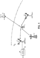
- FIG. 1 shows a wireless device 110 communicating with a wireless communication system 120, in accordance with some exemplary embodiments.
- Wireless communication system 120 may be a Long Term Evolution (LTE) system, a Code Division Multiple Access (CDMA) system, a Global System for Mobile Communications (GSM) system, a wireless local area network (WLAN) system, or some other wireless system.
- a CDMA system may implement Wideband CDMA (WCDMA), CDMA 1X, Evolution-Data Optimized (EVDO), Time Division Synchronous CDMA (TD-SCDMA), or some other version of CDMA.
- WCDMA Wideband CDMA
- CDMA 1X Code Division Multiple Access
- EVDO Evolution-Data Optimized
- TD-SCDMA Time Division Synchronous CDMA
- FIG. 1 shows wireless communication system 120 including two base stations 130 and 132 and one system controller 140.
- a wireless system may include any number of base stations and any set of network entities.
- Wireless device 110 may also be referred to as user equipment (UE), a mobile station, a terminal, an access terminal, a subscriber unit, a station, etc.
- Wireless device 110 may be a cellular phone, a smartphone, a tablet, a wireless modem, a personal digital assistant (PDA), a handheld device, a laptop computer, a smartbook, a netbook, a cordless phone, a wireless local loop (WLL) station, a Bluetooth device, etc.
- Wireless device 110 may communicate with wireless communication system 120.
- Wireless device 110 may also receive signals from broadcast stations (e.g., a broadcast station 134), signals from satellites (e.g., a satellite 150) in one or more global navigation satellite systems (GNSS), etc.
- Wireless device 110 may support one or more radio technologies for wireless communication such as LTE, WCDMA, CDMA 1X, EVDO, TD-SCDMA, GSM, 802.11, etc.
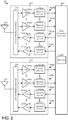
- FIG. 2 shows a block diagram of an exemplary design of wireless device 110 in FIG. 1 .
- wireless device 110 includes a primary transceiver 220 coupled to a primary antenna 210, a secondary transceiver 222 coupled to a secondary antenna 212, and a data processor/controller 280.
- Primary transceiver 220 includes a number (K) of receivers 230pa to 230pk and a number (K) of transmitters 250pa to 250pk to support multiple frequency bands, multiple radio technologies, carrier aggregation, etc.
- Secondary transceiver 222 includes a number (L) of receivers 230sa to 230sl and a number (L) of transmitters 250sa to 250sl to support multiple frequency bands, multiple radio technologies, carrier aggregation, receive diversity, multiple-input multiple-output (MIMO) transmission from multiple transmit antennas to multiple receive antennas, etc.
- L number of receivers 230sa to 230sl
- L number of transmitters 250sa to 250sl to support multiple frequency bands, multiple radio technologies, carrier aggregation, receive diversity, multiple-input multiple-output (MIMO) transmission from multiple transmit antennas to multiple receive antennas, etc.
- MIMO multiple-input multiple-output
- each receiver 230 (e.g., 230pa-230pk and 230sa-230sl) includes a low noise amplifier (LNA) 240 (e.g., 240pa-240pk and 240sa-240sl) and receive circuits 242 (e.g., 242pa-242pk and 242sa-242sl).
- LNA low noise amplifier
- primary antenna 210 receives signals from base stations and/or other transmitter stations and provides a received radio frequency (RF) signal, which is routed through an antenna interface circuit 224 and presented as an input RF signal to a selected receiver.
- Antenna interface circuit 224 may include switches, duplexers, transmit filters, receive filters, matching circuits, etc.
- receiver 230pa is the selected receiver.
- an LNA 240pa amplifies the input RF signal and provides an output RF signal.
- Receive circuits 242pa downconvert the output RF signal from RF to baseband, amplify and filter the downconverted signal, and provide an analog input signal to data processor/controller 280.
- Receive circuits 242pa may include mixers, filters, amplifiers, matching circuits, an oscillator, a local oscillator (LO) generator, a phase locked loop (PLL), etc.
- LO local oscillator
- PLL phase locked loop
- each transmitter 250 (e.g., 250pa-250pk and 250sa-250sl) includes transmit circuits 252 (e.g., 252pa-252pk and 252sa-252sl) and a power amplifier (PA) 254 (e.g., 254pa-254pk and 254sa-254sl).
- PA power amplifier
- data processor/controller 280 processes (e.g., encodes and modulates) data to be transmitted and provides an analog output signal to a selected transmitter. The description below assumes that transmitter 250pa is the selected transmitter.
- transmit circuits 252pa amplify, filter, and upconvert the analog output signal from baseband to RF and provide a modulated RF signal.
- Transmit circuits 252pa may include amplifiers, filters, mixers, matching circuits, an oscillator, an LO generator, a PLL, etc.
- a PA 254pa receives and amplifies the modulated RF signal and provides a transmit RF signal having the proper output power level.
- the transmit RF signal is routed through antenna interface circuit 224 and transmitted via primary antenna 210.
- Each remaining transmitter 250 in transceivers 220 and 222 may operate in similar manner as transmitter 250pa.
- a second RF signal may be routed through antenna interface circuit 226 and transmitted and/or received via secondary antenna 212.
- Each receiver 230 and transmitter 250 may also include other circuits not shown in FIG. 2 , such as filters, matching circuits, etc. All or a portion of transceivers 220 and 222 may be implemented on one or more analog integrated circuits (ICs), RF ICs (RFICs), mixed-signal ICs, etc.
- ICs analog integrated circuits
- RFICs RF ICs
- mixed-signal ICs etc.
- LNAs 240 and receive circuits 242 within transceivers 220 and 222 may be implemented on multiple IC chips, as described below.
- the circuits in transceivers 220 and 222 may also be implemented in other manners.
- Data processor/controller 280 may perform various functions for wireless device 110. For example, data processor/controller 280 may perform processing for data being received via receivers 230 and data being transmitted via transmitters 250. Data processor/controller 280 may control the operation of the various circuits within transceivers 220 and 222. A memory 282 may store program codes and data for data processor/controller 280. Data processor/controller 280 may be implemented on one or more application specific integrated circuits (ASICs) and/or other ICs.
- ASICs application specific integrated circuits
- FIG. 3 is a band diagram 300 depicting three exemplary band groups that may be supported by wireless device 110.
- wireless device 110 may operate in a low-band (LB) including RF signals having frequencies lower than 1000 megahertz (MHz), a mid-band (MB) including RF signals having frequencies from 1000 MHz to 2300 MHz, and/or a high-band (HB) including RF signals having frequencies higher than 2300 MHz.
- LB low-band
- MB mid-band
- HB high-band
- low-band RF signals may cover from 698 MHz to 960 MHz
- mid-band RF signals may cover from 1475 MHz to 2170 MHz
- high-band RF signals may cover from 2300 MHz to 2690 MHz and from 3400 MHz to 3800 MHz, as shown in FIG. 3 .
- Low-band, mid-band, and high-band refer to three groups of bands (or band groups), with each band group including a number of frequency bands (or simply, "bands"). Each band may cover up to 200 MHz.
- LTE Release 11 supports 35 bands, which are referred to as LTE/UMTS bands and are listed in 3GPP TS 36.101.
- Each band group may cover any range of frequencies, which may or may not match any of the frequency ranges shown in FIG. 3 .
- Each band group may also include any number of bands.
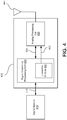
- FIG. 4 is a simplified block diagram of a transceiver 400 that may be included within wireless device 110 of FIG. 2 .
- transceiver 400 may be primary transceiver 220 or secondary transceiver 222.
- Transceiver 400 may exchange digital communication signals 415 with a digital modem 410.
- digital modem 410 may be included within data processor/controller 280.
- Digital modem 410 may provide digital communication signals to transceiver 400, and/or may receive digital communication signals from transceiver 400.
- Transceiver 400 may include a digital baseband processing unit 420 and an analog processing unit 430.
- digital baseband processing unit 420 may convert digital communication signals 415 (e.g., digital transmit and/or receive communication signals) to analog communication signals 453 (e.g., analog transmit and/or receive communication signals).
- a digital transmit communication signal may be received from digital modem 410 by digital baseband processing unit 420.
- the digital transmit communication signal may be processed by a digital-to-analog converter (not shown for simplicity) included within digital baseband processing unit 420 to generate an analog transmit communication signal.
- Analog processing unit 430 may receive the analog transmit communication signal, upconvert, and then transmit the upconverted signal through antenna 440.
- a communication signal may be received by antenna 440, downconverted to an analog receive communication signal by analog processing unit 430, and converted to a digital receive communication signal through an analog-to-digital converter (not shown for simplicity) included within digital baseband processing unit 420.
- digital baseband processing unit 420 may include a correction module 450 to generate a correction signal 452.
- Correction signal 452 may be used to correct one or more impairments associated with the analog transmit communication signal. For example, correction signal 452 may cancel all or part of an intermodulation distortion associated with the analog transmit communication signal, equalize the analog transmit communication signal, and/or pre-distort the analog transmit communication signal. In some embodiments, correction signal 452 may be combined with the analog transmit communication signal within analog processing unit 430. Operation of correction module 450 and generation of correction signal 452 is described in more detail in conjunction with FIGS. 5 - 7 below.
- FIG. 5 is block diagram of another embodiment of a transceiver 500 that may be included within wireless device 110 of FIG. 2 .
- Transceiver 500 may include digital baseband processing unit 520 and analog processing unit 530. Similar to transceiver 400, digital baseband processing unit 520 may convert digital communication signals (e.g., digital baseband signals) from digital modem 410 (not shown for simplicity) to analog communication signals (e.g., analog baseband signals) for analog processing unit 530. Additionally, digital baseband processing unit 520 may convert analog communication signals from analog processing unit 530 to digital communication signals for digital modem 410.
- digital baseband processing unit 520 may convert analog communication signals from analog processing unit 530 to digital communication signals for digital modem 410.
- Digital baseband processing unit 520 may include a digital-to-analog converter (DAC)/analog-to-digital converter (ADC) unit 521, a DAC/ADC unit 522, a correction module 560, and a feedback receiver 525.
- DAC/ADC unit 521 may receive a digital transmit communication signal 571 associated with a first transmitter from digital modem 410 (not shown in FIG. 5 for simplicity).
- DAC/ADC unit 521 may convert digital transmit communication signal 571 to an analog transmit communication signal 573.
- DAC/ADC unit 521 may receive an analog receive communication signal 574 associated with a first receiver and, in response thereto, may generate a digital receive communication signal 572.
- transceiver 500 may support two or more transmitter/receiver pairs.
- DAC/ADC unit 522 may receive a digital transmit communication signal 575 associated with a second transmitter from digital modem 410 and, in response thereto, generate an analog transmit communication signal 577 for analog processing unit 530.
- DAC/ADC unit 522 may also receive an analog receive communication signal 578 associated with a second receiver and, in response thereto, generate a digital receive communication signal 576.
- digital baseband processing unit 520 and analog processing unit 530 may process quadrature and/or differential signals.
- digital transmit communication signal 571 may include two signals: a digital in-phase signal and a digital quadrature signal.
- the digital in-phase signal and the digital quadrature signal may be differential signals.
- Analog processing unit 530 may include a first mixer unit 540, a second mixer unit 545, output selector 550, feedback signal selector 551, amplifiers 552 - 555, a first coupler 556, and a second coupler 557.
- Analog communication signals may be exchanged between digital baseband processing unit 520 and analog processing unit 530.
- analog communication signals associated with a first transmitter/receiver pair e.g., analog transmit communication signal 573 and analog receive communication signal 574
- analog communication signals associated with a second transmitter/receiver pair e.g., analog transmit communication signal 577 and analog receive communication signal 578
- analog communication signals associated with a second transmitter/receiver pair e.g., analog transmit communication signal 577 and analog receive communication signal 578 may be coupled between mixer unit 545 and DAC/ADC unit 522.
- mixer unit 540 may upconvert analog transmit communication signal 573 based on a local oscillator signal (not shown in FIG. 5 for simplicity), and generate a modulated transmit communication signal 580. Mixer unit 540 may also downconvert a modulated receive communication signal 581, and generate analog receive communication signal 574. In some embodiments, modulated transmit communication signal 580 may be buffered by amplifier 553, and a received modulated communication signal 582 may be buffered by amplifier 552. In a similar manner, mixer unit 545 may upconvert analog transmit communication signal 577 and generate a modulated transmit communication signal 583. Mixer unit 545 may also downconvert a modulated receive communication signal 584, and generate analog receive communication signal 578. In some embodiments, modulated transmit communication signal 583 may be buffered by amplifier 555, and a received modulated communication signal 585 may be buffered by amplifier 554.
- Correction module 560 may generate a correction signal 586 to correct one or more impairments that may be associated with a modulated transmit communication signal.
- correction module 560 may be another embodiment of correction module 450 described in FIG. 4 .
- correction signal 586 may be another embodiment of correction signal 452 of FIG. 4 .
- correction signal 586 may correct for an intermodulation distortion caused by another transmit communication signal. For example, when both the first transmitter and the second transmitter operate at or near the same time, the first transmitter may induce a distortion (such as an intermodulation distortion) in the second transmitter.
- Correction module 560 may generate correction signal 586 to counteract (or reduce) the intermodulation distortion in the second transmitter.
- correction signal 586 may correct or counteract one or more non-linearities associated with a transmit communication signal. For example, correction signal 586 may pre-distort or equalize a transmit communication signal.
- Correction module 560 may generate correction signal 586 based on digital transmit communication signal 571, digital receive communication signal 572, digital transmit communication signal 575, digital receive communication signal 576, a digital feedback signal 589, and/or correction module mode control signal 587.
- feedback receiver 525 may receive and demodulate a modulated transmit communication signal, generate a digital feedback signal 589 based on the demodulated transmit communication signal, and provide the digital feedback signal 589 to correction module 560.
- Feedback receiver 525 may be coupled to a feedback signal selector 551.
- Feedback signal selector 551 may select a modulated transmit communication signal associated with the first transmitter or the second transmitter based on a feedback selector control signal 590.
- the modulated analog transmit signal may be provided by amplifier 553 and/or amplifier 555.
- a coupler 556 may provide the modulated analog transmit signal associated with the first transmitter to feedback signal selector 551.
- coupler 557 may provide the modulated analog transmit signal associated with the second transmitter to feedback signal selector 551.
- coupler 556 and coupler 557 may be directional couplers. Operation of correction module 560 and feedback signal selector 551 is described in more detail below in conjunction with FIGS. 6 and 8 .
- Correction signal 586 may be added to a modulated transmit communication signal associated with analog transmit communication signal 573 or a modulated transmit communication signal associated with analog transmit communication signal 577 within mixer unit 540 and mixer unit 545, respectively.
- correction signal 586 may be converted from a digital signal to an analog signal through one or more DACs (not shown for simplicity). Operations of mixer unit 540 and mixer unit 545 are described in more detail below in conjunction with FIG. 7 .
- correction signal 586 may be routed to either mixer unit 540 or mixer unit 545 through output selector 550.
- Output selector 550 may be controlled by output selector control signal 591. Operations of output selector 550 are described in more detail below in conjunction with FIG. 8 .
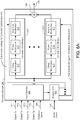
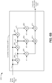
- FIG. 6A is a block diagram of correction module 560, according to some embodiments.
- Correction module 560 may include input selector 602, analysis unit 601, a first correction sub-module 603, a second correction sub-module 604, and summing node 620. Although only first correction sub-module 603 and second correction sub-module 604 are shown, other embodiments of correction module 560 may include other numbers of correction sub-modules (not shown for simplicity). For example, some embodiments of correction module 560 may include a number N of correction sub-modules.
- Each correction sub-module may include a phase modification unit, a delay modification unit, and an amplification modulation unit.
- first correction sub-module 603 may include delay modification unit 610, phase modification unit 611, and amplitude modification unit 612.
- second correction sub-module 604 may include delay modification unit 615, phase modification unit 616, and amplitude modification unit 617.
- Other embodiments of correction sub-units may include fewer than three modification units, additional units, and/or duplicate (e.g., redundant) units.
- a digital communication signal may be provided by input selector 602 to the first correction sub-module 603 and/or the second correction sub-module 604.
- Input selector 602 may receive digital transmit communication signal 571, digital receive communication signal 572, digital transmit communication signal 575, digital receive communication signal 576, and digital feedback signal 589.
- first correction sub-module 603 and/or second correction sub-module 604 may modify, a timing (e.g., delay), a phase, and/or an amplitude of a selected digital communication signal.
- first correction sub-module 603 may adjust a delay of a digital communication signal by delaying the digital communication signal through delay modification unit 610.
- phase modification unit 611 may adjust the phase of the digital communication signal
- amplitude modification unit 612 may increase or decrease an amplitude associated with the digital communication signal.
- a digital communication signal may be modified by second correction sub-module 604.
- delay modification units 610 and 615, phase modification units 611 and 616, and amplitude modification units 612 and 617 may be arranged in any technically feasible order.
- delay, phase, and amplitude modifications may occur in any technically feasible order within first correction sub-module 603 and/or second correction sub-module 604.
- phase, delay, and amplitude modifications may be accomplished by digital filters having a plurality of filter taps.
- delay modification unit 610, phase modification unit 611, and/or amplitude modification unit 612 may each include a digital filter (e.g., a finite impulse response (FIR) or infinite impulse response (IIR) filter) to modify a phase, delay, and amplitude of a digital signal, respectively.
- delay modification unit 615, phase modification unit 616, and amplitude modification unit 617 may each include digital filters.
- an amount of phase modification, delay modification, and/or amplitude modification provided within first correction sub-module 603 and/or second correction sub-module 604 may be determined by sub-module settings provided by analysis unit 601.
- sub-module settings may configure one or more filter taps within the associated correction sub-module.
- sub-module settings for first correction sub-module 603 may configure filter taps within delay modification unit 610, phase modification unit 611, and/or amplitude modification unit 612.
- sub-module settings for second correction sub-module 604 may configure filter taps within delay modification unit 615, phase modification unit 616, and/or amplitude modification unit 617.
- output signals from each correction sub-module may be summed together at summing node 620 to generate correction signal 586.
- correction module 560 may be configured to generate a correction signal 586 based on an operating mode. For example, some operating modes may generate correction signal 586 to reduce or attenuate an intermodulation distortion. Intermodulation distortion may be caused by an aggressor signal interfering with a victim signal. For example, a first modulated transmit communication signal (the aggressor signal) may interfere with a second modulated transmit communication signal (the victim signal). In another example, the second modulated transmit communication signal (the aggressor signal) may interfere with the first modulated transmit communication signal (the victim signal). Thus, in some embodiments, correction signal 586 may be configured to reduce interference from an aggressor signal to one or more victim signals.
- initial sub-module settings for first correction sub-module 603 and/or second correction sub-module 604 may be determined by analysis unit 601 to reduce or attenuate an intermodulation distortion.
- the victim signal may be modulated transmit communication signal 580 and the aggressor signal may be modulated transmit communication signal 583 (see also FIG. 5 ).
- Initial sub-module settings may be based on the aggressor signal received at analysis unit 601.
- input selector 602 may provide digital transmit communication signal 575 to first correction sub-module 603 and second correction sub-module 604, and may provide digital feedback signal 589 to analysis unit 601.
- the digital feedback signal 589 may be associated with the victim signal (e.g., modulated transmit communication signal 580).
- eq. 1 expresses that a received signal may include two components during an initialization period (e.g., when the victim transmitter is not transmitting): a first component due to leaking paths (intermodulation, for example) and a second component due to the cancelling signal g(t).
- an initial value of the cancelling signal g(t) may be determined. For example, while the transmitter associated with the victim signal is on, but not transmitting data, a received signal (digital feedback signal 589) may be recorded by analysis unit 601. Analysis unit 601 may then determine cancelling signal g(t) and, moreover, may determine how to generate g(t) based on the aggressor signal. In other embodiments, repeated sampling and estimations may be used to determine cancelling signal g(t). For example, least-mean-square (LMS) and/or recursive-least-squares (RLS) operations may be used to determine cancelling signal g(t). In still other embodiments, a combination of LMS, RLS and/or eq. 6 may be used.
- LMS least-mean-square
- RLS recursive-least-squares
- analysis unit 601 may determine sub-module settings to generate cancelling signal g(t) (e.g., using eq. 6).
- cancelling signal g(t) may describe and/or be associated with tap values for digital filters (e.g., FIR or IIR filters) within correction sub-module 603 and/or correction sub-module 604.
- more than one correction sub-module may be used to generate cancelling signal g(t).
- analysis unit 601 may determine sub-module settings for a plurality of correction sub-modules to generate cancelling signal g(t) (e.g., correction signal 586).
- First correction sub-module 603 and/or second correction sub-module 604 may modify digital transmit communication signal 575 and generate correction signal 586.
- Correction signal 586 may be added to the victim signal (e.g., modulated transmit communication signal 580 within mixer unit 540) to reduce or attenuate intermodulation distortion.
- sub-module settings for first correction sub-module 603 and second correction sub-module 604 may be determined by analysis unit 601 to reduce or attenuate intermodulation distortion.
- the second operating mode may update and/or refine initial sub-module settings determined during the first operating mode.
- the victim signal may be modulated transmit communication signal 580 and the aggressor signal may be modulated transmit communication signal 583.
- Input selector 602 may provide digital transmit communication signal 575 to first correction sub-module 603 and second correction sub-module 604.
- Input selector 602 may provide digital receive communication signal 572 or digital receive communication signal 576 to analysis unit 601.
- Analysis unit 601 may use digital receive communication signal 572 or digital receive communication signal 576 to determine settings for first correction sub-module 603 and/or second correction sub-module 604.
- first correction sub-module 603 and/or second correction sub-module 604 may modify digital transmit communication signal 571 and generate correction signal 586 to reduce or attenuate intermodulation distortion.
- Correction signal 586 may be added to analog transmit communication signal 573 within mixer unit 540.
- Analysis unit 601 may determine updated sub-module settings for first correction sub-module 603 and/or second correction sub-module 604 using the procedures described above in the first operating mode or any other technically feasible method.
- a bit error rate or noise floor measurements associated with the victim signal may be used to determine new sub-module settings. For example, LMS and/or RLS iterations to determine sub-module settings may be repeated until the victim signal has a bit error rate or a noise floor measurement less than a predetermined threshold.
- the victim signal is modulated transmit communication signal 580
- the aggressor signal is modulated transmit communication signal 583
- Other modes may support other victim and aggressor signals.
- a third operating mode may determine initial sub-module settings for first correction sub-module 603 and/or second correction sub-module 604 when the victim signal is modulated transmit communication signal 583 and the aggressor signal is modulated transmit communication signal 580.
- updated sub-module settings for first correction sub-module 603 and/or second correction sub-module 604 may be determined by analysis unit 601 to reduce or attenuate intermodulation distortion.
- Settings and operations for the third operating mode and the fourth operating mode may be determined in a similar manner as described above for the first operating mode and the second operating mode.
- different signals may be coupled to first correction sub-module 603, second correction sub-module 604, and analysis unit 601 as described in Table 1 in conjunction with FIG. 8 below.
- correction module 560 may be configured to generate a correction signal 586 to equalize the output of the first transmitter.
- correction signal 586 may correct for impairments caused by signal processing associated with the first transmitter.
- signal processing characteristics associated with the first transmitter may be determined during a bench test or a simulation.
- settings e.g., settings associated with equalizing signals for the first transmitter
- first correction sub-module 603 and/or second correction sub-module 604 may be determined based on the bench test and/or simulation results, and may be stored within analysis unit 601.
- mixer unit 540 and/or amplifier 553 may have been characterized and may have an undesired frequency response.
- Input selector 602 may provide digital transmit communication signal 571 to first correction sub-module 603 and/or second correction sub-module 604.
- Analysis unit 601 may also receive modulated transmit communication signal 580 through digital feedback signal 589.
- Analysis unit 601 may determine settings for first correction sub-module 603 and/or second correction sub-module 604 based on digital feedback signal 589 and retrieved settings associated with equalizing signals for the first transmitter.
- first correction sub-module 603 and/or second correction sub-module 604 may modify digital transmit communication signal 571 to generate correction signal 586.
- correction signal 586 may be added to analog transmit communication signal 573 within mixer unit 540.
- correction signal 586 may be a digital signal and may be added to digital transmit communication signal 571 prior to DAC/ADC unit 521.
- correction module 560 may configure correction module 560 to generate a correction signal 586 to equalize the output of the second transmitter.
- mixer unit 545 and/or amplifier 555 may have been characterized and may have an undesired frequency response.
- Input selector 602 may provide digital transmit communication signal 575 to first correction sub-module 603 and/or second correction sub-module 604.
- Analysis unit 601 may also receive modulated transmit communication signal 583 through digital feedback signal 589.
- Analysis unit 601 may determine settings for first correction sub-module 603 and/or second correction sub-module 604 based on digital feedback signal 589 and retrieved settings associated with equalizing signals for the second transmitter.
- first correction sub-module 603 and/or second correction sub-module 604 may modify digital transmit communication signal 575 to generate correction signal 586.
- correction signal 586 may be added to analog transmit communication signal 577 within mixer unit 545.
- correction signal 586 may be a digital signal and may be simply added to digital transmit communication signal 575 prior to DAC/ADC unit 522.
- correction module 560 may be configured to generate a correction signal 586 to pre-distort signals to be output through the first transmitter (e.g., digital transmit communication signal 571).
- a digital transmit communication signal may be modified to correct for known impairments associated with some signal processing.
- Input selector 602 may provide digital transmit communication signal 571 to first correction sub-module 603 and/or second correction sub-module 604.
- Analysis unit 601 may retrieve stored settings associated with pre-distorting signals for the first transmitter for first correction sub-module 603 and/or second correction sub-module 604.
- Analysis unit 601 may also receive modulated transmit communication signal 580 through digital feedback signal 589 (via input selector 602).
- Analysis unit 601 may determine settings for first correction sub-module 603 and/or second correction sub-module 604 based on digital feedback signal 589 and/or retrieved settings associated with pre-distorting signals for the first transmitter. Thus, first correction sub-module 603 and/or second correction sub-module 604 may modify digital transmit communication signal 571 to generate correction signal 586. Correction signal 586 may be added to analog transmit communication signal 573 within mixer unit 540.
- correction module 560 may be configured to generate correction signal 586 to pre-distort signals to be output through the second transmitter.
- correction module 560 may be configured to generate correction signal 586 to pre-distort signals for the second transmitter (e.g., digital transmit communication signal 575).
- Input selector 602 may provide digital transmit communication signal 575 to first correction sub-module 603 and/or second correction sub-module 604.
- Analysis unit 601 may retrieve stored settings associated with pre-distorting signals for the second transmitter for first correction sub-module 603 and/or second correction sub-module 604.
- Analysis unit 601 may also receive modulated transmit communication signal 583 through digital feedback signal 589.
- Analysis unit 601 may determine settings for first correction sub-module 603 and/or second correction sub-module 604 based on digital feedback signal 589 and/or retrieved settings associated with pre-distorting signals for the second transmitter. Thus, first correction sub-module 603 and/or second correction sub-module 604 may modify digital transmit communication signal 575 to generate correction signal 586. Correction signal 586 may be added to analog transmit communication signal 577 within mixer unit 545.
- FIG. 6B is a block diagram 650 of another embodiment of a correction sub-module 651 of FIG. 6A .
- Correction sub-module 651 may include multipliers 660 - 665 and adders 670 - 671. Although only six multipliers and two adders are shown, other embodiments of correction sub-module 651 may include other numbers of multipliers and adders.
- Correction sub-module 651 may receive a signal from input selector 602 and may generate a non-linear correction sub-module output signal 675 (e.g., a correction signal having a non-linear frequency response) for correction module 560 (see FIG. 6A ).
- non-linear frequency responses may be used to pre-distort a transmit communication signal.
- multipliers 660 - 662 may receive the signal from input selector 602 and progressively generate associated exponential signals. For example, an input signal x may be received at two inputs of multiplier 660. In response, multiplier 660 may generate an output signal x 2 . In a similar manner, multiplier 661 may generate an output signal x 3 and multiplier 662 may generate an output signal x 4 . Additional multipliers (not shown for simplicity) may be used to generate additional non-linear terms.
- Output signals from multipliers 660 - 662 may be provided to multipliers 663 - 665.
- Multipliers 663 - 665 may multiply each output signal from multipliers 660 - 662 by a gain coefficient (shown as A1 - A3 for multipliers 663 - 665, respectively).
- Gain coefficients A1 - A3 may control an amount of influence (e.g., weight) that each output signal from multipliers 660 - 662 has on correction sub-module output signal 675.
- sub-module settings associated with correction sub-module 651 may determine values of gain coefficients A1 - A3.
- Adders 670 and 671 may add together output signals from multipliers 663 - 665 to generate the correction sub-module output signal 675.
- a correction sub-module may include both delay, phase, and amplitude modification units 610 - 612 and multipliers 660 - 665 and adders 670 - 671.
- FIG. 7 is a block diagram 700 of mixer unit 540, in accordance with some embodiments.
- Mixer unit 540 may include a first mixer 701, second mixer 702, a third mixer 705, a fourth mixer 706, a first summing node 703, a second summing node 707, a third summing node 710, and local oscillator 704.
- Mixer unit 540 may receive analog transmit communication signal 573 and correction signal 586 (via output selector 550, not shown for in FIG. 7 simplicity).
- Mixer unit 540 may generate modulated transmit communication signal 580.
- analog transmit communication signal 573 may be a quadrature signal having an analog transmit in-phase signal 720 and an analog transmit quadrature signal 721.
- correction signal 586 may be a quadrature signal having a correction in-phase signal 722 and a correction quadrature signal 723.
- analog transmit in-phase signal 720, analog transmit quadrature signal 721, correction in-phase signal 722, and/or correction quadrature signal 723 may be differential signals (not shown for simplicity).
- Mixer unit 540 may modulate one or more signals based on signals provided by local oscillator 704.
- local oscillator 704 may generate a local oscillator (LO) signal having a frequency associated with a carrier frequency.
- local oscillator 704 may generate quadrature LO signals including an LO in-phase (I) signal and a LO quadrature (Q) signal.
- local oscillator 704 may generate differential LO signals (not shown for simplicity).
- analog transmit communication signal 573 may be "mixed” with an LO signal to generate a partial modulated transmit communication signal 708.
- a mixer may "mix” together two input signals (e.g., multiply two signals together), and generate an output signal based on a product of the two input signals.
- individual I and Q signals may be mixed independently. Therefore, analog transmit in-phase signal 720 may be mixed with LO (I) signal by first mixer 701, and analog transmit quadrature signal 721 may be mixed with LO (Q) signal by second mixer 702. Output signals from first mixer 701 and second mixer 702 may be summed together by first summing node 703 to generate the partial modulated transmit communication signal 708.
- correction signal 586 may be mixed with the LO signal to generate a partial modulated transmit communication signal 709.
- correction in-phase signal 722 may be mixed with LO (I) signal by third mixer 705, and correction quadrature signal 723 may be mixed with LO (Q) signal by fourth mixer 706.
- Output signals from third mixer 705 and fourth mixer 706 may be summed together by second summing node 707 to generate partial modulated transmit communication signal 709.
- Third summing node 710 may sum together partial modulated transmit communication signal 708 and partial modulated transmit communication signal 709 to generate modulated transmit communication signal 580 (e.g., to generate a corrected communication signal).
- Mixer unit 545 may be substantially similar to mixer unit 540.
- FIG. 8A is a block diagram of a correction module controller 800, in accordance with some embodiments.
- Correction module controller 800 may be included within transceiver 400, transceiver 500, and/or within correction module 560.
- correction module controller 800 may control, at least in part, operations of correction module 560, output selector 550, and/or feedback signal selector 551.
- Correction module controller 800 may include control block 810 and signal generator 815.
- Control block 810 may generate a mode control signal 812 that may cause transceiver 400 or transceiver 500 to operate in one or more of the operating modes described above.
- control block 810 may generate mode control signal 812 to operate transceiver 500 in a first operating mode to determine initial sub-module settings for first correction sub-module 603 and second correction sub-module 604 to reduce or attenuate intermodulation distortion.
- the mode control signal 812 may be determined based on an aggressor signal and a victim signal.
- the mode control signal 812 may be determined based on a desired equalization or pre-distortion correction to be applied.
- Signal generator 815 may receive mode control signal 812 and, in response thereto, may generate correction module mode control signal 587, feedback selector control signal 590, and/or output selector control signal 591.
- the correction module mode control signal 587 may determine one or more operations within analysis unit 601.
- feedback selector control signal 590 may determine which signal (from coupler 556 or coupler 557) is to be coupled to feedback receiver 525.
- output selector control signal 591 may determine which mixer unit (mixer unit 540 or mixer unit 545) receives correction signal 586 from correction module 560.
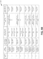
- FIG. 8B shows an illustrative table 850 that describes exemplary modes and configurations for transceiver 500 including input sources for first correction sub-module 603, second correction sub-module 604, and analysis unit 601.
- Table 850 also shows settings associated with feedback signal selector 551 and output selector 550.
- Table 850 is not meant as an exhaustive list of all possible operating modes and configurations, but instead shows exemplary mode and configurations for transceiver 500.
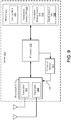
- FIG. 9 depicts a device 900 that is another exemplary embodiment of wireless device 110 of FIG. 2 .
- Device 900 includes a transceiver 910, a correction module 920, a processor 930, and a memory 940.
- transceiver 910 may be similar to one or more exemplary embodiments of transceiver 400 or transceiver 500 described above in conjunction with FIG. 4 and FIG.5 , respectively.
- transceiver 910 may be similar to primary transceiver 220 and/or secondary transceiver 222 described above in conjunction with FIG. 2 .
- transceiver 910 may be a multi-band transceiver capable of supporting carrier aggregation, which is simultaneous operation on multiple carriers (e.g., carrier frequencies).
- transceiver 910 may include a first transmitter 903 and a second transmitter 904 to transmit and receive communication signals through different carrier frequencies.
- Correction module 920 may generate a correction signal 586 to correct one or more impairments associated with a transmit communication signal. For example, in one embodiment, correction module 920 may generate correction signal 586 to reduce or attenuate an intermodulation distortion associated with a modulated transmit communication signal. In another embodiment, correction module 920 may generate correction signal 586 to equalize and/or pre-distort a transmit communication signal. Correction module 920 may include one or more correction sub-modules, such as first correction sub-module 603 and/or second correction sub-module 604 (see FIG. 6A ).
- Memory 940 may include a look up table 942 that may be used to store one or more sub-module settings for correction module 920.
- sub-module settings associated with pre-distorting a transmit communication signal may be stored within look up table 942.
- sub-module settings associated with equalizing a transmit communication signal may be stored within look up table 942.
- Memory 940 may also include a non-transitory computer-readable storage medium (e.g., one or more nonvolatile memory elements, such as EPROM, EEPROM, Flash memory, a hard drive, etc.) that may store the following software modules:
- a non-transitory computer-readable storage medium e.g., one or more nonvolatile memory elements, such as EPROM, EEPROM, Flash memory, a hard drive, etc.
- Each software module includes program instructions that, when executed by processor 930, may cause the device 900 to perform the corresponding function(s).
- the non-transitory computer-readable storage medium of memory 940 may include instructions for performing all or a portion of the operations of FIG. 10 .
- Processor 930 which is coupled to transceiver 910, correction module 920, and memory 940, may be any one or more suitable processors capable of executing scripts or instructions of one or more software programs stored in device 900 (e.g., within memory 940).
- Transceiver control software 944 may select one or more frequency bands within which to operate transceiver 910.
- transceiver control software 944 may select a 2.4 GHz frequency band to operate transmitter 903 and may select a 900 MHz frequency band to operate transmitter 904.
- transceiver 910 may operate within other frequency bands.
- Processor 930 may execute correction module control software 946 to determine operating modes for correction module 920. For example, correction module control software 946 may operate correction module 920 in a first operating mode to reduce intermodulation distortion within a first transmit communication signal. In another example, correction module control software 946 may operate correction module 920 in a fifth operating mode to equalize a first transmit communication signal.
- the operating modes listed herein are merely exemplary and are not meant to be limiting.
- Processor 930 may execute signal analysis software 948 to analyze a communication signal and determine one or more sub-module settings for first correction sub-module 603 and/or second correction sub-module 604 based on the communication signal.
- signal analysis software 948 may analyze an aggressor signal and determine sub-module settings to generate a correction signal 586 to reduce or attenuate the effects of the aggressor signal on the victim signal.
- signal analysis software 948 may analyze a communication signal and determine sub-module settings to generate a correction signal 586 to equalize and/or pre-distort the communication signal.
- FIG. 10 shows an illustrative flow chart depicting an exemplary operation 1000 for wireless device 110, in accordance with some embodiments.
- an operating mode of correction module 560 is determined (1002).
- the operating mode may be based on a desired correction signal 586.
- the operating mode may be determined, at least in part, by correction signal 586 to reduce or attenuate an intermodulation distortion associated with a first communication signal, to equalize the first communication signal, and/or to pre-distort the first communication signal.
- the operating mode may also be determined by the aggressor signal and the victim signal.
- sub-module settings are determined based on the operating mode (1004). For example, the operating mode of correction module 560 may be selected to pre-distort the first communication signal. Thus, the sub-module settings for pre-distorting the first communication signal may be retrieved from look up table 942 and used to configure correction module 560 to perform the pre-distortion of the first communication signal. In other examples, other sub-module settings may be determined based on other operating modes.
- determining sub-module settings 1004 may also include an optional analysis of a communication signal (1006).
- the analysis of the communication signal may aid in the determining of the sub-module settings. For example, if the operating mode of correction module 560 is to generate correction signal 586 to reduce or attenuate intermodulation distortion due to the aggressor signal, then the aggressor signal may be analyzed by analysis unit 601. In another example, if the operating mode of correction module 560 is to generate a correction signal 586 to equalize the first communication signal, then the first communication signal may be analyzed by analysis unit 601. In other examples, other signals may be analyzed by analysis unit 601.
- correction signal 586 is generated (1008).
- correction signal 586 may be generated by one or more correction sub-modules 603 - 604 configured by sub-module settings determined at 1004.
- a corrected communication signal is generated (1010).
- the corrected communication signal may be generated by summing a communication signal with correction signal 586.
- an update of the sub-module settings is determined (1012). If sub-modules settings are to be updated, then operations proceed to 1002. If sub-module settings are not to be changed, then operations proceed to 1012 to continue to check if sub-module settings are to be updated.
- DSP Digital Signal Processor
- ASIC Application Specific Integrated Circuit
- FPGA Field Programmable Gate Array
- a general purpose processor may be a microprocessor, but in the alternative, the processor may be any conventional processor, controller, microcontroller, or state machine.
- a processor may also be implemented as a combination of computing devices, e.g., a combination of a DSP and a microprocessor, a plurality of microprocessors, one or more microprocessors in conjunction with a DSP core, or any other such configuration.
- the functions described may be implemented in hardware, software, firmware, or any combination thereof. If implemented in software, the functions may be stored on or transmitted over as one or more instructions or code on a computer-readable medium.
- Computer-readable media includes both computer storage media and communication media including any medium that facilitates transfer of a computer program from one place to another.
- a storage media may be any available media that can be accessed by a computer.
- such computer-readable media can comprise RAM, ROM, EEPROM, CD-ROM or other optical disk storage, magnetic disk storage or other magnetic storage devices, or any other medium that can be used to carry or store desired program code in the form of instructions or data structures and that can be accessed by a computer.
- any connection is properly termed a computer-readable medium.
- the software is transmitted from a website, server, or other remote source using a coaxial cable, fiber optic cable, twisted pair, digital subscriber line (DSL), or wireless technologies such as infrared, radio, and microwave
- the coaxial cable, fiber optic cable, twisted pair, DSL, or wireless technologies such as infrared, radio, and microwave are included in the definition of medium.
- Disk and disc includes compact disc (CD), laser disc, optical disc, digital versatile disc (DVD), floppy disk, and blu-ray disc where disks usually reproduce data magnetically, while discs reproduce data optically with lasers. Combinations of the above should also be included within the scope of computer-readable media.
Landscapes
- Engineering & Computer Science (AREA)
- Computer Networks & Wireless Communication (AREA)
- Signal Processing (AREA)
- Transmitters (AREA)
Description
- The exemplary embodiments relate generally to wireless communications, and specifically to signal correction for wireless devices supporting carrier aggregation.
-
WO 2014/136437 A1 discusses the problem that in wireless transmission devices that transmit a plurality of bands of RF signal, the amount of distortion of output signals increases due to differences in lag time in a plurality of pathways. To solve this problem the document describes a multiband RF signal generator that carries a plurality of input baseband signals at carrier waves each having a different frequency, and outputs the result as a wireless frequency signal; a power amplifier that amplifies and outputs the wireless frequency signal; a unit for generating a distortion compensation control signal that subjects each of the plurality of input baseband signals to a distortion compensation function that compensates for the distortion characteristics of the power amplifier: and a transmitter lag correction unit that corrects the differences in lag time incurred by each of the plurality of input baseband signals in the multiband RF signal generator. -
EP 1 102 418 A1 - A wireless device (e.g., a cellular phone or a smartphone) in a wireless communication system may transmit and receive data for two-way communication. The wireless device may include a transmitter for data transmission and a receiver for data reception. For data transmission, the transmitter may modulate a radio frequency (RF) carrier signal with data to generate a modulated RF signal, amplify the modulated RF signal to generate a transmit RF signal having the proper output power level, and transmit the transmit RF signal via an antenna to a base station. For data reception, the receiver may obtain a received RF signal via the antenna and may amplify and process the received RF signal to recover data sent by the base station.
- The wireless device may support two-way communication on multiple frequency bands and/or multiple radio technologies. The wireless device may also support carrier aggregation, which is simultaneous operation on multiple carriers. A carrier may refer to a range of frequencies used for two-way communication and may be associated with certain characteristics. For example, a carrier may be associated with a communication system (e.g., Wi-Fi, cellular) and/or a communication protocol (e.g., IEEE 802.11, BLUETOOTH, LTE, etc.) A carrier may also be referred to as a component carrier (CC), a frequency channel, a cell, etc.
- When multiple transmitters operate simultaneously, communication signals associated with a first transmitter may undesirably interfere with communication signals associated with a second transmitter. For example, communication signals from the second transmitter may cause intermodulation distortion in the first communication signal.
- Thus, there is a need to improve performance of multiple transmitters in wireless devices, especially wireless devices supporting carrier aggregation.
- The present embodiments are illustrated by way of example and are not intended to be limited by the figures of the accompanying drawings. Like numbers reference like elements throughout the drawings and specification.
-
FIG. 1 shows a wireless device communicating with a wireless communication system, in accordance with some exemplary embodiments. -
FIG. 2 shows an exemplary design of a receiver and a transmitter ofFIG. 1 . -
FIG. 3 is a band diagram depicting three exemplary band groups that may be supported by the wireless device ofFIG. 1 . -
FIG. 4 is a simplified block diagram of a transceiver included within the wireless device ofFIG. 2 . -
FIG. 5 is a block diagram of another embodiment of a transceiver included within the wireless device ofFIG. 2 . -
FIG. 6A is a block diagram of a correction module, according to some embodiments. -
FIG. 6B is a block diagram of another embodiment of a correction sub-module ofFIG. 6A . -
FIG. 7 is a block diagram of a mixer unit ofFIG. 5 , in accordance with some embodiments. -
FIG. 8A is a block diagram of a correction module controller, in accordance with some embodiments. -
FIG. 8B is an illustrative table depicting exemplary modes of operation for the transceiver ofFIG. 5 . -
FIG. 9 depicts a device that is another exemplary embodiment of the wireless device ofFIG. 2 . -
FIG. 10 shows an illustrative flow chart depicting an exemplary operation for the wireless device ofFIG. 1 , in accordance with some embodiments. - In the following description, numerous specific details are set forth such as examples of specific components, circuits, and processes to provide a thorough understanding of the present disclosure. The term "coupled" as used herein means coupled directly to or coupled through one or more intervening components or circuits. Also, in the following description and for purposes of explanation, specific nomenclature and/or details are set forth to provide a thorough understanding of the present embodiments. However, it will be apparent to one skilled in the art that these specific details may not be required to practice the present embodiments. In other instances, well-known circuits and devices are shown in block diagram form to avoid obscuring the present disclosure. Any of the signals provided over various buses described herein may be time-multiplexed with other signals and provided over one or more common buses. Additionally, the interconnection between circuit elements or software blocks may be shown as buses or as single signal lines. Each of the buses may alternatively be a single signal line, and each of the single signal lines may alternatively be buses, and a single line or bus might represent any one or more of a myriad of physical or logical mechanisms for communication between components. The present embodiments are not to be construed as limited to specific examples described herein but rather to include within their scope all embodiments defined by the appended claims.
- In addition, the detailed description set forth below in connection with the appended drawings is intended as a description of exemplary embodiments of the present disclosure and is not intended to represent the only embodiments in which the present disclosure may be practiced. The term "exemplary" used throughout this description means "serving as an example, instance, or illustration," and should not necessarily be construed as preferred or advantageous over other embodiments.
-
FIG. 1 shows awireless device 110 communicating with awireless communication system 120, in accordance with some exemplary embodiments.Wireless communication system 120 may be a Long Term Evolution (LTE) system, a Code Division Multiple Access (CDMA) system, a Global System for Mobile Communications (GSM) system, a wireless local area network (WLAN) system, or some other wireless system. A CDMA system may implement Wideband CDMA (WCDMA), CDMA 1X, Evolution-Data Optimized (EVDO), Time Division Synchronous CDMA (TD-SCDMA), or some other version of CDMA. For simplicity,FIG. 1 showswireless communication system 120 including twobase stations system controller 140. In general, a wireless system may include any number of base stations and any set of network entities. -
Wireless device 110 may also be referred to as user equipment (UE), a mobile station, a terminal, an access terminal, a subscriber unit, a station, etc.Wireless device 110 may be a cellular phone, a smartphone, a tablet, a wireless modem, a personal digital assistant (PDA), a handheld device, a laptop computer, a smartbook, a netbook, a cordless phone, a wireless local loop (WLL) station, a Bluetooth device, etc.Wireless device 110 may communicate withwireless communication system 120.Wireless device 110 may also receive signals from broadcast stations (e.g., a broadcast station 134), signals from satellites (e.g., a satellite 150) in one or more global navigation satellite systems (GNSS), etc.Wireless device 110 may support one or more radio technologies for wireless communication such as LTE, WCDMA, CDMA 1X, EVDO, TD-SCDMA, GSM, 802.11, etc. -
FIG. 2 shows a block diagram of an exemplary design ofwireless device 110 inFIG. 1 . In this exemplary design,wireless device 110 includes aprimary transceiver 220 coupled to aprimary antenna 210, asecondary transceiver 222 coupled to asecondary antenna 212, and a data processor/controller 280.Primary transceiver 220 includes a number (K) of receivers 230pa to 230pk and a number (K) of transmitters 250pa to 250pk to support multiple frequency bands, multiple radio technologies, carrier aggregation, etc.Secondary transceiver 222 includes a number (L) of receivers 230sa to 230sl and a number (L) of transmitters 250sa to 250sl to support multiple frequency bands, multiple radio technologies, carrier aggregation, receive diversity, multiple-input multiple-output (MIMO) transmission from multiple transmit antennas to multiple receive antennas, etc. - In the exemplary design shown in
FIG. 2 , each receiver 230 (e.g., 230pa-230pk and 230sa-230sl) includes a low noise amplifier (LNA) 240 (e.g., 240pa-240pk and 240sa-240sl) and receive circuits 242 (e.g., 242pa-242pk and 242sa-242sl). For data reception,primary antenna 210 receives signals from base stations and/or other transmitter stations and provides a received radio frequency (RF) signal, which is routed through anantenna interface circuit 224 and presented as an input RF signal to a selected receiver.Antenna interface circuit 224 may include switches, duplexers, transmit filters, receive filters, matching circuits, etc. The description below assumes that receiver 230pa is the selected receiver. Within receiver 230pa, an LNA 240pa amplifies the input RF signal and provides an output RF signal. Receive circuits 242pa downconvert the output RF signal from RF to baseband, amplify and filter the downconverted signal, and provide an analog input signal to data processor/controller 280. Receive circuits 242pa may include mixers, filters, amplifiers, matching circuits, an oscillator, a local oscillator (LO) generator, a phase locked loop (PLL), etc. Each remaining receiver 230 intransceivers - In the exemplary design shown in
FIG. 2 , each transmitter 250 (e.g., 250pa-250pk and 250sa-250sl) includes transmit circuits 252 (e.g., 252pa-252pk and 252sa-252sl) and a power amplifier (PA) 254 (e.g., 254pa-254pk and 254sa-254sl). For data transmission, data processor/controller 280 processes (e.g., encodes and modulates) data to be transmitted and provides an analog output signal to a selected transmitter. The description below assumes that transmitter 250pa is the selected transmitter. Within transmitter 250pa, transmit circuits 252pa amplify, filter, and upconvert the analog output signal from baseband to RF and provide a modulated RF signal. Transmit circuits 252pa may include amplifiers, filters, mixers, matching circuits, an oscillator, an LO generator, a PLL, etc. A PA 254pa receives and amplifies the modulated RF signal and provides a transmit RF signal having the proper output power level. The transmit RF signal is routed throughantenna interface circuit 224 and transmitted viaprimary antenna 210. Each remaining transmitter 250 intransceivers antenna interface circuit 226 and transmitted and/or received viasecondary antenna 212. - Each receiver 230 and transmitter 250 may also include other circuits not shown in
FIG. 2 , such as filters, matching circuits, etc. All or a portion oftransceivers transceivers transceivers - Data processor/
controller 280 may perform various functions forwireless device 110. For example, data processor/controller 280 may perform processing for data being received via receivers 230 and data being transmitted via transmitters 250. Data processor/controller 280 may control the operation of the various circuits withintransceivers memory 282 may store program codes and data for data processor/controller 280. Data processor/controller 280 may be implemented on one or more application specific integrated circuits (ASICs) and/or other ICs. -
FIG. 3 is a band diagram 300 depicting three exemplary band groups that may be supported bywireless device 110. In some embodiments,wireless device 110 may operate in a low-band (LB) including RF signals having frequencies lower than 1000 megahertz (MHz), a mid-band (MB) including RF signals having frequencies from 1000 MHz to 2300 MHz, and/or a high-band (HB) including RF signals having frequencies higher than 2300 MHz. For example, low-band RF signals may cover from 698 MHz to 960 MHz, mid-band RF signals may cover from 1475 MHz to 2170 MHz, and high-band RF signals may cover from 2300 MHz to 2690 MHz and from 3400 MHz to 3800 MHz, as shown inFIG. 3 . Low-band, mid-band, and high-band refer to three groups of bands (or band groups), with each band group including a number of frequency bands (or simply, "bands"). Each band may cover up to 200 MHz. LTE Release 11 supports 35 bands, which are referred to as LTE/UMTS bands and are listed in 3GPP TS 36.101. - In general, any number of band groups may be defined. Each band group may cover any range of frequencies, which may or may not match any of the frequency ranges shown in
FIG. 3 . Each band group may also include any number of bands. -
FIG. 4 is a simplified block diagram of atransceiver 400 that may be included withinwireless device 110 ofFIG. 2 . For example,transceiver 400 may beprimary transceiver 220 orsecondary transceiver 222.Transceiver 400 may exchange digital communication signals 415 with adigital modem 410. In some embodiments,digital modem 410 may be included within data processor/controller 280.Digital modem 410 may provide digital communication signals totransceiver 400, and/or may receive digital communication signals fromtransceiver 400. -
Transceiver 400 may include a digitalbaseband processing unit 420 and ananalog processing unit 430. In some embodiments, digitalbaseband processing unit 420 may convert digital communication signals 415 (e.g., digital transmit and/or receive communication signals) to analog communication signals 453 (e.g., analog transmit and/or receive communication signals). For example, a digital transmit communication signal may be received fromdigital modem 410 by digitalbaseband processing unit 420. The digital transmit communication signal may be processed by a digital-to-analog converter (not shown for simplicity) included within digitalbaseband processing unit 420 to generate an analog transmit communication signal.Analog processing unit 430 may receive the analog transmit communication signal, upconvert, and then transmit the upconverted signal throughantenna 440. In a similar manner, a communication signal may be received byantenna 440, downconverted to an analog receive communication signal byanalog processing unit 430, and converted to a digital receive communication signal through an analog-to-digital converter (not shown for simplicity) included within digitalbaseband processing unit 420. - In some embodiments, digital
baseband processing unit 420 may include acorrection module 450 to generate acorrection signal 452.Correction signal 452 may be used to correct one or more impairments associated with the analog transmit communication signal. For example,correction signal 452 may cancel all or part of an intermodulation distortion associated with the analog transmit communication signal, equalize the analog transmit communication signal, and/or pre-distort the analog transmit communication signal. In some embodiments,correction signal 452 may be combined with the analog transmit communication signal withinanalog processing unit 430. Operation ofcorrection module 450 and generation ofcorrection signal 452 is described in more detail in conjunction withFIGS. 5 - 7 below. -
FIG. 5 is block diagram of another embodiment of atransceiver 500 that may be included withinwireless device 110 ofFIG. 2 .Transceiver 500 may include digitalbaseband processing unit 520 andanalog processing unit 530. Similar totransceiver 400, digitalbaseband processing unit 520 may convert digital communication signals (e.g., digital baseband signals) from digital modem 410 (not shown for simplicity) to analog communication signals (e.g., analog baseband signals) foranalog processing unit 530. Additionally, digitalbaseband processing unit 520 may convert analog communication signals fromanalog processing unit 530 to digital communication signals fordigital modem 410. - Digital
baseband processing unit 520 may include a digital-to-analog converter (DAC)/analog-to-digital converter (ADC)unit 521, a DAC/ADC unit 522, acorrection module 560, and afeedback receiver 525. DAC/ADC unit 521 may receive a digital transmitcommunication signal 571 associated with a first transmitter from digital modem 410 (not shown inFIG. 5 for simplicity). DAC/ADC unit 521 may convert digital transmitcommunication signal 571 to an analog transmitcommunication signal 573. Additionally, DAC/ADC unit 521 may receive an analog receivecommunication signal 574 associated with a first receiver and, in response thereto, may generate a digital receivecommunication signal 572. In some embodiments,transceiver 500 may support two or more transmitter/receiver pairs. Thus, DAC/ADC unit 522 may receive a digital transmitcommunication signal 575 associated with a second transmitter fromdigital modem 410 and, in response thereto, generate an analog transmitcommunication signal 577 foranalog processing unit 530. DAC/ADC unit 522 may also receive an analog receivecommunication signal 578 associated with a second receiver and, in response thereto, generate a digital receivecommunication signal 576. Persons skilled in the art will appreciate that digitalbaseband processing unit 520 andanalog processing unit 530 may process quadrature and/or differential signals. For example, digital transmitcommunication signal 571 may include two signals: a digital in-phase signal and a digital quadrature signal. Furthermore, in some embodiments, the digital in-phase signal and the digital quadrature signal may be differential signals. -
Analog processing unit 530 may include afirst mixer unit 540, asecond mixer unit 545,output selector 550,feedback signal selector 551, amplifiers 552 - 555, afirst coupler 556, and asecond coupler 557. Analog communication signals may be exchanged between digitalbaseband processing unit 520 andanalog processing unit 530. Thus, analog communication signals associated with a first transmitter/receiver pair (e.g., analog transmitcommunication signal 573 and analog receive communication signal 574) may be coupled betweenmixer unit 540 and DAC/ADC unit 521. In a similar manner, analog communication signals associated with a second transmitter/receiver pair (e.g., analog transmitcommunication signal 577 and analog receive communication signal 578) may be coupled betweenmixer unit 545 and DAC/ADC unit 522. - In some embodiments,
mixer unit 540 may upconvert analog transmitcommunication signal 573 based on a local oscillator signal (not shown inFIG. 5 for simplicity), and generate a modulated transmitcommunication signal 580.Mixer unit 540 may also downconvert a modulated receivecommunication signal 581, and generate analog receivecommunication signal 574. In some embodiments, modulated transmitcommunication signal 580 may be buffered byamplifier 553, and a received modulatedcommunication signal 582 may be buffered byamplifier 552. In a similar manner,mixer unit 545 may upconvert analog transmitcommunication signal 577 and generate a modulated transmitcommunication signal 583.Mixer unit 545 may also downconvert a modulated receivecommunication signal 584, and generate analog receivecommunication signal 578. In some embodiments, modulated transmitcommunication signal 583 may be buffered byamplifier 555, and a received modulatedcommunication signal 585 may be buffered byamplifier 554. -
Correction module 560 may generate acorrection signal 586 to correct one or more impairments that may be associated with a modulated transmit communication signal. In some embodiments,correction module 560 may be another embodiment ofcorrection module 450 described inFIG. 4 . In a similar manner,correction signal 586 may be another embodiment ofcorrection signal 452 ofFIG. 4 . In one embodiment,correction signal 586 may correct for an intermodulation distortion caused by another transmit communication signal. For example, when both the first transmitter and the second transmitter operate at or near the same time, the first transmitter may induce a distortion (such as an intermodulation distortion) in the second transmitter.Correction module 560 may generatecorrection signal 586 to counteract (or reduce) the intermodulation distortion in the second transmitter. In another embodiment,correction signal 586 may correct or counteract one or more non-linearities associated with a transmit communication signal. For example,correction signal 586 may pre-distort or equalize a transmit communication signal. -
Correction module 560 may generate correction signal 586 based on digital transmitcommunication signal 571, digital receivecommunication signal 572, digital transmitcommunication signal 575, digital receivecommunication signal 576, adigital feedback signal 589, and/or correction modulemode control signal 587. In some embodiments,feedback receiver 525 may receive and demodulate a modulated transmit communication signal, generate adigital feedback signal 589 based on the demodulated transmit communication signal, and provide thedigital feedback signal 589 tocorrection module 560.Feedback receiver 525 may be coupled to afeedback signal selector 551.Feedback signal selector 551 may select a modulated transmit communication signal associated with the first transmitter or the second transmitter based on a feedbackselector control signal 590. In some embodiments, the modulated analog transmit signal may be provided byamplifier 553 and/oramplifier 555. Acoupler 556 may provide the modulated analog transmit signal associated with the first transmitter tofeedback signal selector 551. In a similar manner,coupler 557 may provide the modulated analog transmit signal associated with the second transmitter tofeedback signal selector 551. In some embodiments,coupler 556 andcoupler 557 may be directional couplers. Operation ofcorrection module 560 andfeedback signal selector 551 is described in more detail below in conjunction withFIGS. 6 and8 . -
Correction signal 586 may be added to a modulated transmit communication signal associated with analog transmitcommunication signal 573 or a modulated transmit communication signal associated with analog transmitcommunication signal 577 withinmixer unit 540 andmixer unit 545, respectively. In some embodiments,correction signal 586 may be converted from a digital signal to an analog signal through one or more DACs (not shown for simplicity). Operations ofmixer unit 540 andmixer unit 545 are described in more detail below in conjunction withFIG. 7 . In some embodiments,correction signal 586 may be routed to eithermixer unit 540 ormixer unit 545 throughoutput selector 550.Output selector 550 may be controlled by outputselector control signal 591. Operations ofoutput selector 550 are described in more detail below in conjunction withFIG. 8 . -
FIG. 6A is a block diagram ofcorrection module 560, according to some embodiments.Correction module 560 may includeinput selector 602,analysis unit 601, afirst correction sub-module 603, asecond correction sub-module 604, and summingnode 620. Although onlyfirst correction sub-module 603 andsecond correction sub-module 604 are shown, other embodiments ofcorrection module 560 may include other numbers of correction sub-modules (not shown for simplicity). For example, some embodiments ofcorrection module 560 may include a number N of correction sub-modules. - Each correction sub-module may include a phase modification unit, a delay modification unit, and an amplification modulation unit. For example,
first correction sub-module 603 may includedelay modification unit 610,phase modification unit 611, andamplitude modification unit 612. In a similar manner,second correction sub-module 604 may includedelay modification unit 615,phase modification unit 616, andamplitude modification unit 617. Other embodiments of correction sub-units may include fewer than three modification units, additional units, and/or duplicate (e.g., redundant) units. - A digital communication signal may be provided by
input selector 602 to thefirst correction sub-module 603 and/or thesecond correction sub-module 604.Input selector 602 may receive digital transmitcommunication signal 571, digital receivecommunication signal 572, digital transmitcommunication signal 575, digital receivecommunication signal 576, anddigital feedback signal 589. In one embodiment,first correction sub-module 603 and/orsecond correction sub-module 604 may modify, a timing (e.g., delay), a phase, and/or an amplitude of a selected digital communication signal. For example,first correction sub-module 603 may adjust a delay of a digital communication signal by delaying the digital communication signal throughdelay modification unit 610. Additionally,phase modification unit 611 may adjust the phase of the digital communication signal, andamplitude modification unit 612 may increase or decrease an amplitude associated with the digital communication signal. In a similar manner, a digital communication signal may be modified bysecond correction sub-module 604. Although depicted in an exemplary order inFIG. 6A , in other embodiments, delaymodification units phase modification units amplitude modification units first correction sub-module 603 and/orsecond correction sub-module 604. - In some embodiments, phase, delay, and amplitude modifications may be accomplished by digital filters having a plurality of filter taps. For example, delay
modification unit 610,phase modification unit 611, and/oramplitude modification unit 612 may each include a digital filter (e.g., a finite impulse response (FIR) or infinite impulse response (IIR) filter) to modify a phase, delay, and amplitude of a digital signal, respectively. In a similar manner, delaymodification unit 615,phase modification unit 616, andamplitude modification unit 617 may each include digital filters. - In some embodiments, an amount of phase modification, delay modification, and/or amplitude modification provided within
first correction sub-module 603 and/orsecond correction sub-module 604 may be determined by sub-module settings provided byanalysis unit 601. In some embodiments, sub-module settings may configure one or more filter taps within the associated correction sub-module. For example, sub-module settings forfirst correction sub-module 603 may configure filter taps withindelay modification unit 610,phase modification unit 611, and/oramplitude modification unit 612. In a similar manner, sub-module settings forsecond correction sub-module 604 may configure filter taps withindelay modification unit 615,phase modification unit 616, and/oramplitude modification unit 617. In some embodiments, output signals from each correction sub-module may be summed together at summingnode 620 to generatecorrection signal 586. - In one embodiment,
correction module 560 may be configured to generate acorrection signal 586 based on an operating mode. For example, some operating modes may generatecorrection signal 586 to reduce or attenuate an intermodulation distortion. Intermodulation distortion may be caused by an aggressor signal interfering with a victim signal. For example, a first modulated transmit communication signal (the aggressor signal) may interfere with a second modulated transmit communication signal (the victim signal). In another example, the second modulated transmit communication signal (the aggressor signal) may interfere with the first modulated transmit communication signal (the victim signal). Thus, in some embodiments,correction signal 586 may be configured to reduce interference from an aggressor signal to one or more victim signals. - In a first operating mode (e.g., calibration mode), initial sub-module settings for
first correction sub-module 603 and/orsecond correction sub-module 604 may be determined byanalysis unit 601 to reduce or attenuate an intermodulation distortion. The victim signal may be modulated transmitcommunication signal 580 and the aggressor signal may be modulated transmit communication signal 583 (see alsoFIG. 5 ). Initial sub-module settings may be based on the aggressor signal received atanalysis unit 601. Thus,input selector 602 may provide digital transmitcommunication signal 575 tofirst correction sub-module 603 andsecond correction sub-module 604, and may providedigital feedback signal 589 toanalysis unit 601. In some embodiments, thedigital feedback signal 589 may be associated with the victim signal (e.g., modulated transmit communication signal 580). - In some embodiments, during initialization, a received signal r(t) may be expressed with eq. 1 below:

- where h(t) is a function describing leaking paths;
- x(t) is a function describing an aggressor signal; and
- g(t) is a function describing the cancelling signal.
- Thus, eq. 1 expresses that a received signal may include two components during an initialization period (e.g., when the victim transmitter is not transmitting): a first component due to leaking paths (intermodulation, for example) and a second component due to the cancelling signal g(t). To determine the first component due to leaking paths, the cancelling signal g(t) component may be set to zero as shown in eq. 2:

- Next, the received signal may be recorded (e.g., a number M samples of received signal may be recorded) by
analysis unit 601 yielding eq. 3 below:
- Thus, for cancelling signal g(t) to remove affects from the aggressor signal:

- Since received signal r(t) may include a discrete number of samples M associated with the recording described above, r(t) may be expressed as a vector, as shown in eq. 5 below:

- Thus, solving for cancelling signal g(t) is shown in eq. 6, below:

- In this manner, an initial value of the cancelling signal g(t) may be determined. For example, while the transmitter associated with the victim signal is on, but not transmitting data, a received signal (digital feedback signal 589) may be recorded by
analysis unit 601.Analysis unit 601 may then determine cancelling signal g(t) and, moreover, may determine how to generate g(t) based on the aggressor signal. In other embodiments, repeated sampling and estimations may be used to determine cancelling signal g(t). For example, least-mean-square (LMS) and/or recursive-least-squares (RLS) operations may be used to determine cancelling signal g(t). In still other embodiments, a combination of LMS, RLS and/or eq. 6 may be used. - Thus,
analysis unit 601 may determine sub-module settings to generate cancelling signal g(t) (e.g., using eq. 6). In some embodiments, cancelling signal g(t) may describe and/or be associated with tap values for digital filters (e.g., FIR or IIR filters) withincorrection sub-module 603 and/orcorrection sub-module 604. In some embodiments, more than one correction sub-module may be used to generate cancelling signal g(t). Thus,analysis unit 601 may determine sub-module settings for a plurality of correction sub-modules to generate cancelling signal g(t) (e.g., correction signal 586).First correction sub-module 603 and/orsecond correction sub-module 604 may modify digital transmitcommunication signal 575 and generatecorrection signal 586.Correction signal 586 may be added to the victim signal (e.g., modulated transmitcommunication signal 580 within mixer unit 540) to reduce or attenuate intermodulation distortion. - In a second operating mode (e.g., normal operating mode), sub-module settings for
first correction sub-module 603 andsecond correction sub-module 604 may be determined byanalysis unit 601 to reduce or attenuate intermodulation distortion. In contrast to the first operating mode, the second operating mode may update and/or refine initial sub-module settings determined during the first operating mode. Similar to the first operating mode, the victim signal may be modulated transmitcommunication signal 580 and the aggressor signal may be modulated transmitcommunication signal 583.Input selector 602 may provide digital transmitcommunication signal 575 tofirst correction sub-module 603 andsecond correction sub-module 604.Input selector 602 may provide digital receivecommunication signal 572 or digital receivecommunication signal 576 toanalysis unit 601.Analysis unit 601 may use digital receivecommunication signal 572 or digital receivecommunication signal 576 to determine settings forfirst correction sub-module 603 and/orsecond correction sub-module 604. Thus,first correction sub-module 603 and/orsecond correction sub-module 604 may modify digital transmitcommunication signal 571 and generatecorrection signal 586 to reduce or attenuate intermodulation distortion.Correction signal 586 may be added to analog transmitcommunication signal 573 withinmixer unit 540. -
Analysis unit 601 may determine updated sub-module settings forfirst correction sub-module 603 and/orsecond correction sub-module 604 using the procedures described above in the first operating mode or any other technically feasible method. In some embodiments, a bit error rate or noise floor measurements associated with the victim signal may be used to determine new sub-module settings. For example, LMS and/or RLS iterations to determine sub-module settings may be repeated until the victim signal has a bit error rate or a noise floor measurement less than a predetermined threshold. - In the first operating mode and the second operating mode described above, the victim signal is modulated transmit
communication signal 580, and the aggressor signal is modulated transmitcommunication signal 583. Other modes may support other victim and aggressor signals. For example, a third operating mode may determine initial sub-module settings forfirst correction sub-module 603 and/orsecond correction sub-module 604 when the victim signal is modulated transmitcommunication signal 583 and the aggressor signal is modulated transmitcommunication signal 580. In a similar manner, in a fourth operating mode, updated sub-module settings forfirst correction sub-module 603 and/orsecond correction sub-module 604 may be determined byanalysis unit 601 to reduce or attenuate intermodulation distortion. Settings and operations for the third operating mode and the fourth operating mode may be determined in a similar manner as described above for the first operating mode and the second operating mode. In the third operating mode and the fourth operating mode, different signals may be coupled tofirst correction sub-module 603,second correction sub-module 604, andanalysis unit 601 as described in Table 1 in conjunction withFIG. 8 below. - In a fifth operating mode,
correction module 560 may be configured to generate acorrection signal 586 to equalize the output of the first transmitter. Thus, instead of correcting impairments caused by an aggressor signal,correction signal 586 may correct for impairments caused by signal processing associated with the first transmitter. In some embodiments, signal processing characteristics associated with the first transmitter may be determined during a bench test or a simulation. Thus, settings (e.g., settings associated with equalizing signals for the first transmitter) that may be applied tofirst correction sub-module 603 and/orsecond correction sub-module 604 may be determined based on the bench test and/or simulation results, and may be stored withinanalysis unit 601. - For example, referring also to
FIG. 5 ,mixer unit 540 and/oramplifier 553 may have been characterized and may have an undesired frequency response.Input selector 602 may provide digital transmitcommunication signal 571 tofirst correction sub-module 603 and/orsecond correction sub-module 604.Analysis unit 601 may also receive modulated transmitcommunication signal 580 throughdigital feedback signal 589.Analysis unit 601 may determine settings forfirst correction sub-module 603 and/orsecond correction sub-module 604 based ondigital feedback signal 589 and retrieved settings associated with equalizing signals for the first transmitter. Thus,first correction sub-module 603 and/orsecond correction sub-module 604 may modify digital transmitcommunication signal 571 to generatecorrection signal 586. In one embodiment,correction signal 586 may be added to analog transmitcommunication signal 573 withinmixer unit 540. In another embodiment,correction signal 586 may be a digital signal and may be added to digital transmitcommunication signal 571 prior to DAC/ADC unit 521. - Other operating modes may configure
correction module 560 to generate acorrection signal 586 to equalize the output of the second transmitter. For example, referring also toFIG. 5 , in a sixth operating mode,mixer unit 545 and/oramplifier 555 may have been characterized and may have an undesired frequency response.Input selector 602 may provide digital transmitcommunication signal 575 tofirst correction sub-module 603 and/orsecond correction sub-module 604.Analysis unit 601 may also receive modulated transmitcommunication signal 583 throughdigital feedback signal 589.Analysis unit 601 may determine settings forfirst correction sub-module 603 and/orsecond correction sub-module 604 based ondigital feedback signal 589 and retrieved settings associated with equalizing signals for the second transmitter. Thus,first correction sub-module 603 and/orsecond correction sub-module 604 may modify digital transmitcommunication signal 575 to generatecorrection signal 586. In one embodiment,correction signal 586 may be added to analog transmitcommunication signal 577 withinmixer unit 545. In another embodiment,correction signal 586 may be a digital signal and may be simply added to digital transmitcommunication signal 575 prior to DAC/ADC unit 522. - In a seventh operating mode,
correction module 560 may be configured to generate acorrection signal 586 to pre-distort signals to be output through the first transmitter (e.g., digital transmit communication signal 571). In some embodiments, a digital transmit communication signal may be modified to correct for known impairments associated with some signal processing.Input selector 602 may provide digital transmitcommunication signal 571 tofirst correction sub-module 603 and/orsecond correction sub-module 604.Analysis unit 601 may retrieve stored settings associated with pre-distorting signals for the first transmitter forfirst correction sub-module 603 and/orsecond correction sub-module 604.Analysis unit 601 may also receive modulated transmitcommunication signal 580 through digital feedback signal 589 (via input selector 602).Analysis unit 601 may determine settings forfirst correction sub-module 603 and/orsecond correction sub-module 604 based ondigital feedback signal 589 and/or retrieved settings associated with pre-distorting signals for the first transmitter. Thus,first correction sub-module 603 and/orsecond correction sub-module 604 may modify digital transmitcommunication signal 571 to generatecorrection signal 586.Correction signal 586 may be added to analog transmitcommunication signal 573 withinmixer unit 540. - Other operating modes may configure
correction module 560 to generate acorrection signal 586 to pre-distort signals to be output through the second transmitter. For example, in an eighth operating mode,correction module 560 may be configured to generatecorrection signal 586 to pre-distort signals for the second transmitter (e.g., digital transmit communication signal 575).Input selector 602 may provide digital transmitcommunication signal 575 tofirst correction sub-module 603 and/orsecond correction sub-module 604.Analysis unit 601 may retrieve stored settings associated with pre-distorting signals for the second transmitter forfirst correction sub-module 603 and/orsecond correction sub-module 604.Analysis unit 601 may also receive modulated transmitcommunication signal 583 throughdigital feedback signal 589.Analysis unit 601 may determine settings forfirst correction sub-module 603 and/orsecond correction sub-module 604 based ondigital feedback signal 589 and/or retrieved settings associated with pre-distorting signals for the second transmitter. Thus,first correction sub-module 603 and/orsecond correction sub-module 604 may modify digital transmitcommunication signal 575 to generatecorrection signal 586.Correction signal 586 may be added to analog transmitcommunication signal 577 withinmixer unit 545. - Although exemplary operating modes are described above, these operating modes are merely illustrative and are not meant to be limiting.
-
FIG. 6B is a block diagram 650 of another embodiment of acorrection sub-module 651 ofFIG. 6A .Correction sub-module 651 may include multipliers 660 - 665 and adders 670 - 671. Although only six multipliers and two adders are shown, other embodiments of correction sub-module 651 may include other numbers of multipliers and adders. -
Correction sub-module 651 may receive a signal frominput selector 602 and may generate a non-linear correction sub-module output signal 675 (e.g., a correction signal having a non-linear frequency response) for correction module 560 (seeFIG. 6A ). In some embodiments, non-linear frequency responses may be used to pre-distort a transmit communication signal. In some embodiments, multipliers 660 - 662 may receive the signal frominput selector 602 and progressively generate associated exponential signals. For example, an input signal x may be received at two inputs ofmultiplier 660. In response,multiplier 660 may generate an output signal x2. In a similar manner,multiplier 661 may generate an output signal x3 andmultiplier 662 may generate an output signal x4. Additional multipliers (not shown for simplicity) may be used to generate additional non-linear terms. - Output signals from multipliers 660 - 662 may be provided to multipliers 663 - 665. Multipliers 663 - 665 may multiply each output signal from multipliers 660 - 662 by a gain coefficient (shown as A1 - A3 for multipliers 663 - 665, respectively). Gain coefficients A1 - A3 may control an amount of influence (e.g., weight) that each output signal from multipliers 660 - 662 has on correction
sub-module output signal 675. Thus, in some embodiments, sub-module settings associated with correction sub-module 651 may determine values of gain coefficients A1 - A3.Adders sub-module output signal 675. - In other embodiments, different non-linear frequency responses may be provided by different numbers of multipliers and different configurations of multipliers 660 - 665 and adders 670 - 671 within
correction sub-module 651. In still other embodiments, a correction sub-module may include both delay, phase, and amplitude modification units 610 - 612 and multipliers 660 - 665 and adders 670 - 671. -
FIG. 7 is a block diagram 700 ofmixer unit 540, in accordance with some embodiments.Mixer unit 540 may include afirst mixer 701,second mixer 702, athird mixer 705, afourth mixer 706, a first summingnode 703, a second summingnode 707, a third summingnode 710, andlocal oscillator 704.Mixer unit 540 may receive analog transmitcommunication signal 573 and correction signal 586 (viaoutput selector 550, not shown for inFIG. 7 simplicity).Mixer unit 540 may generate modulated transmitcommunication signal 580. In some embodiments, analog transmitcommunication signal 573 may be a quadrature signal having an analog transmit in-phase signal 720 and an analog transmitquadrature signal 721. In a similar manner,correction signal 586 may be a quadrature signal having a correction in-phase signal 722 and acorrection quadrature signal 723. In some embodiments, analog transmit in-phase signal 720, analog transmitquadrature signal 721, correction in-phase signal 722, and/orcorrection quadrature signal 723 may be differential signals (not shown for simplicity). -
Mixer unit 540 may modulate one or more signals based on signals provided bylocal oscillator 704. In some embodiments,local oscillator 704 may generate a local oscillator (LO) signal having a frequency associated with a carrier frequency. In other embodiments,local oscillator 704 may generate quadrature LO signals including an LO in-phase (I) signal and a LO quadrature (Q) signal. In still other embodiments,local oscillator 704 may generate differential LO signals (not shown for simplicity). - In some embodiments, analog transmit
communication signal 573 may be "mixed" with an LO signal to generate a partial modulated transmitcommunication signal 708. A mixer may "mix" together two input signals (e.g., multiply two signals together), and generate an output signal based on a product of the two input signals. In some embodiments, individual I and Q signals may be mixed independently. Therefore, analog transmit in-phase signal 720 may be mixed with LO (I) signal byfirst mixer 701, and analog transmitquadrature signal 721 may be mixed with LO (Q) signal bysecond mixer 702. Output signals fromfirst mixer 701 andsecond mixer 702 may be summed together by first summingnode 703 to generate the partial modulated transmitcommunication signal 708. - In a similar manner,
correction signal 586 may be mixed with the LO signal to generate a partial modulated transmitcommunication signal 709. For example, correction in-phase signal 722 may be mixed with LO (I) signal bythird mixer 705, andcorrection quadrature signal 723 may be mixed with LO (Q) signal byfourth mixer 706. Output signals fromthird mixer 705 andfourth mixer 706 may be summed together by second summingnode 707 to generate partial modulated transmitcommunication signal 709. Third summingnode 710 may sum together partial modulated transmitcommunication signal 708 and partial modulated transmitcommunication signal 709 to generate modulated transmit communication signal 580 (e.g., to generate a corrected communication signal).Mixer unit 545 may be substantially similar tomixer unit 540. -
FIG. 8A is a block diagram of acorrection module controller 800, in accordance with some embodiments.Correction module controller 800 may be included withintransceiver 400,transceiver 500, and/or withincorrection module 560. In some embodiments,correction module controller 800 may control, at least in part, operations ofcorrection module 560,output selector 550, and/orfeedback signal selector 551. -
Correction module controller 800 may includecontrol block 810 andsignal generator 815.Control block 810 may generate amode control signal 812 that may causetransceiver 400 ortransceiver 500 to operate in one or more of the operating modes described above. For example, control block 810 may generatemode control signal 812 to operatetransceiver 500 in a first operating mode to determine initial sub-module settings forfirst correction sub-module 603 andsecond correction sub-module 604 to reduce or attenuate intermodulation distortion. In some embodiments, themode control signal 812 may be determined based on an aggressor signal and a victim signal. In other embodiments, themode control signal 812 may be determined based on a desired equalization or pre-distortion correction to be applied. -
Signal generator 815 may receivemode control signal 812 and, in response thereto, may generate correction modulemode control signal 587, feedbackselector control signal 590, and/or outputselector control signal 591. In some embodiments, the correction modulemode control signal 587 may determine one or more operations withinanalysis unit 601. In other embodiments, feedbackselector control signal 590 may determine which signal (fromcoupler 556 or coupler 557) is to be coupled tofeedback receiver 525. In still other embodiments, outputselector control signal 591 may determine which mixer unit (mixer unit 540 or mixer unit 545) receivescorrection signal 586 fromcorrection module 560. -
FIG. 8B shows an illustrative table 850 that describes exemplary modes and configurations fortransceiver 500 including input sources forfirst correction sub-module 603,second correction sub-module 604, andanalysis unit 601. Table 850 also shows settings associated withfeedback signal selector 551 andoutput selector 550. Table 850 is not meant as an exhaustive list of all possible operating modes and configurations, but instead shows exemplary mode and configurations fortransceiver 500. -
FIG. 9 depicts adevice 900 that is another exemplary embodiment ofwireless device 110 ofFIG. 2 .Device 900 includes atransceiver 910, acorrection module 920, aprocessor 930, and amemory 940. In some embodiments,transceiver 910 may be similar to one or more exemplary embodiments oftransceiver 400 ortransceiver 500 described above in conjunction withFIG. 4 andFIG.5 , respectively. In other embodiments,transceiver 910 may be similar toprimary transceiver 220 and/orsecondary transceiver 222 described above in conjunction withFIG. 2 . In some embodiments,transceiver 910 may be a multi-band transceiver capable of supporting carrier aggregation, which is simultaneous operation on multiple carriers (e.g., carrier frequencies). In one embodiment,transceiver 910 may include afirst transmitter 903 and asecond transmitter 904 to transmit and receive communication signals through different carrier frequencies. -
Correction module 920 may generate acorrection signal 586 to correct one or more impairments associated with a transmit communication signal. For example, in one embodiment,correction module 920 may generatecorrection signal 586 to reduce or attenuate an intermodulation distortion associated with a modulated transmit communication signal. In another embodiment,correction module 920 may generatecorrection signal 586 to equalize and/or pre-distort a transmit communication signal.Correction module 920 may include one or more correction sub-modules, such asfirst correction sub-module 603 and/or second correction sub-module 604 (seeFIG. 6A ). -
Memory 940 may include a look up table 942 that may be used to store one or more sub-module settings forcorrection module 920. In one embodiment, sub-module settings associated with pre-distorting a transmit communication signal may be stored within look up table 942. In another embodiment, sub-module settings associated with equalizing a transmit communication signal may be stored within look up table 942. -
Memory 940 may also include a non-transitory computer-readable storage medium (e.g., one or more nonvolatile memory elements, such as EPROM, EEPROM, Flash memory, a hard drive, etc.) that may store the following software modules: - transceiver control software 944 to select frequency bands within which to operate
transceiver 910; - correction module control software 946 to determine operating modes for
correction module 920; and -
signal analysis software 948 to analyze a communication signal and determine one or more settings for correction sub-modules included withincorrection module 920. - Each software module includes program instructions that, when executed by
processor 930, may cause thedevice 900 to perform the corresponding function(s). Thus, the non-transitory computer-readable storage medium ofmemory 940 may include instructions for performing all or a portion of the operations ofFIG. 10 . -
Processor 930, which is coupled totransceiver 910,correction module 920, andmemory 940, may be any one or more suitable processors capable of executing scripts or instructions of one or more software programs stored in device 900 (e.g., within memory 940). -
Processor 930 may execute transceiver control software 944 to select one or more frequency bands within which to operatetransceiver 910. For example, transceiver control software 944 may select a 2.4 GHz frequency band to operatetransmitter 903 and may select a 900 MHz frequency band to operatetransmitter 904. In other embodiments,transceiver 910 may operate within other frequency bands. -
Processor 930 may execute correction module control software 946 to determine operating modes forcorrection module 920. For example, correction module control software 946 may operatecorrection module 920 in a first operating mode to reduce intermodulation distortion within a first transmit communication signal. In another example, correction module control software 946 may operatecorrection module 920 in a fifth operating mode to equalize a first transmit communication signal. The operating modes listed herein are merely exemplary and are not meant to be limiting. -
Processor 930 may executesignal analysis software 948 to analyze a communication signal and determine one or more sub-module settings forfirst correction sub-module 603 and/orsecond correction sub-module 604 based on the communication signal. In some embodiments,signal analysis software 948 may analyze an aggressor signal and determine sub-module settings to generate acorrection signal 586 to reduce or attenuate the effects of the aggressor signal on the victim signal. In other embodiments,signal analysis software 948 may analyze a communication signal and determine sub-module settings to generate acorrection signal 586 to equalize and/or pre-distort the communication signal. -
FIG. 10 shows an illustrative flow chart depicting anexemplary operation 1000 forwireless device 110, in accordance with some embodiments. Referring also toFIGS. 5 ,6 ,8 , and9 , an operating mode ofcorrection module 560 is determined (1002). In some embodiments, the operating mode may be based on a desiredcorrection signal 586. For example, the operating mode may be determined, at least in part, bycorrection signal 586 to reduce or attenuate an intermodulation distortion associated with a first communication signal, to equalize the first communication signal, and/or to pre-distort the first communication signal. Additionally, in some embodiments, the operating mode may also be determined by the aggressor signal and the victim signal. - Next, sub-module settings are determined based on the operating mode (1004). For example, the operating mode of
correction module 560 may be selected to pre-distort the first communication signal. Thus, the sub-module settings for pre-distorting the first communication signal may be retrieved from look up table 942 and used to configurecorrection module 560 to perform the pre-distortion of the first communication signal. In other examples, other sub-module settings may be determined based on other operating modes. - In some embodiments, determining
sub-module settings 1004 may also include an optional analysis of a communication signal (1006). The analysis of the communication signal may aid in the determining of the sub-module settings. For example, if the operating mode ofcorrection module 560 is to generatecorrection signal 586 to reduce or attenuate intermodulation distortion due to the aggressor signal, then the aggressor signal may be analyzed byanalysis unit 601. In another example, if the operating mode ofcorrection module 560 is to generate acorrection signal 586 to equalize the first communication signal, then the first communication signal may be analyzed byanalysis unit 601. In other examples, other signals may be analyzed byanalysis unit 601. - Next,
correction signal 586 is generated (1008). In some embodiments,correction signal 586 may be generated by one or more correction sub-modules 603 - 604 configured by sub-module settings determined at 1004. Next, a corrected communication signal is generated (1010). In some embodiments, the corrected communication signal may be generated by summing a communication signal withcorrection signal 586. - Next, an update of the sub-module settings is determined (1012). If sub-modules settings are to be updated, then operations proceed to 1002. If sub-module settings are not to be changed, then operations proceed to 1012 to continue to check if sub-module settings are to be updated.
- The various illustrative logical blocks, modules, and circuits described in connection with the embodiments disclosed herein may be implemented or performed with a general purpose processor, a Digital Signal Processor (DSP), an Application Specific Integrated Circuit (ASIC), a Field Programmable Gate Array (FPGA) or other programmable logic device, discrete gate or transistor logic, discrete hardware components, or any combination thereof designed to perform the functions described herein. A general purpose processor may be a microprocessor, but in the alternative, the processor may be any conventional processor, controller, microcontroller, or state machine. A processor may also be implemented as a combination of computing devices, e.g., a combination of a DSP and a microprocessor, a plurality of microprocessors, one or more microprocessors in conjunction with a DSP core, or any other such configuration.
- In one or more exemplary embodiments, the functions described may be implemented in hardware, software, firmware, or any combination thereof. If implemented in software, the functions may be stored on or transmitted over as one or more instructions or code on a computer-readable medium. Computer-readable media includes both computer storage media and communication media including any medium that facilitates transfer of a computer program from one place to another. A storage media may be any available media that can be accessed by a computer. By way of example, and not limitation, such computer-readable media can comprise RAM, ROM, EEPROM, CD-ROM or other optical disk storage, magnetic disk storage or other magnetic storage devices, or any other medium that can be used to carry or store desired program code in the form of instructions or data structures and that can be accessed by a computer. Also, any connection is properly termed a computer-readable medium. For example, if the software is transmitted from a website, server, or other remote source using a coaxial cable, fiber optic cable, twisted pair, digital subscriber line (DSL), or wireless technologies such as infrared, radio, and microwave, then the coaxial cable, fiber optic cable, twisted pair, DSL, or wireless technologies such as infrared, radio, and microwave are included in the definition of medium. Disk and disc, as used herein, includes compact disc (CD), laser disc, optical disc, digital versatile disc (DVD), floppy disk, and blu-ray disc where disks usually reproduce data magnetically, while discs reproduce data optically with lasers. Combinations of the above should also be included within the scope of computer-readable media.
- In the foregoing specification, the present embodiments have been described with reference to specific exemplary embodiments thereof. It will, however, be evident that various modifications and changes may be made thereto without departing from the scope of the disclosure as set forth in the appended claims. The specification and drawings are, accordingly, to be regarded in an illustrative sense rather than a restrictive sense.
Claims (12)
- An apparatus (500) comprising:means for generating a first portion of a correction signal (586) to modify a first transmit communication signal (571) via a first correction sub-module (603) based at least in part on an operating mode of the apparatus; means for generating a mode control signal (587) via a control block (810); andmeans for determining via an analysis unit (601) sub-module settings to control the first correction sub-module based at least in part on a second transmit communication signal (575) and the mode control signal.
- The apparatus (500) of claim 1, wherein the first transmit communication signal is a digital baseband signal (571) for a first transmitter, and the second transmit communication signal is a digital baseband signal (575) for a second transmitter.
- The apparatus (500) of claim 1, further comprising:
means (602) for selecting the second transmit communication signal (575) from a plurality of communication signals. - The apparatus (500) of claim 1, wherein the correction signal (586) is configured to attenuate an intermodulation distortion associated with the first transmit communication signal (571).
- The apparatus (500) of claim 1, wherein the correction signal (586) is configured to equalize the first transmit communication signal (571).
- The apparatus (500) of claim 1, wherein the correction signal (586) is configured to pre-distort the first transmit communication signal (571).
- The apparatus (500) of claim 1, further comprising:
means for generating a second portion of the correction signal to modify the first transmit communication signal (571) via a second correction sub-module (604). - The apparatus (500) of claim 1, wherein the means for generating a first portion of a correction signal (586) is further configured to:modify a phase associated with the second transmit communication signal (575);modify a time associated with the second transmit communication signal; andmodify an amplitude associated with the second transmit communication signal.
- The apparatus (500) of claim 1, wherein the means for determining sub-module settings via an analysis unit (601) is further configured to determine initial correction sub-module settings based on analyzing the second transmit communication signal (575).
- The apparatus (500) of claim 1, wherein the first correction sub-module (603) is configured to perform at least one operation selected from the group consisting of intermodulation cancelation, equalization of a digital transmit signal, and pre-distortion of a digital transmit signal based at least in part on the mode control signal (587).
- The apparatus (500) of claim 1, wherein the mode control signal (587) is based on at least one signal selected from the group consisting of an aggressor signal and a victim signal.
- A non-transitory computer-readable medium storing instructions that, when executed by a processor of an apparatus (500) causes the apparatus to:generate, by a first correction sub-module (603), a first portion of a correction signal (586) to modify a first transmit communication signal (571) based at least in part on an operating mode of the apparatus;generate, by a control block (810), a mode control signal (587); anddetermine, by an analysis unit (601), sub-module setting to control the first correction sub-module based at least in part on a second transmit communication signal (575) and the mode control signal.
Applications Claiming Priority (2)
| Application Number | Priority Date | Filing Date | Title |
|---|---|---|---|
| US14/668,823 US9762266B2 (en) | 2015-03-25 | 2015-03-25 | Signal correction for carrier aggregation transceiver |
| PCT/US2016/021628 WO2016153787A1 (en) | 2015-03-25 | 2016-03-09 | Signal correction for carrier aggregation transceiver |
Publications (2)
| Publication Number | Publication Date |
|---|---|
| EP3275081A1 EP3275081A1 (en) | 2018-01-31 |
| EP3275081B1 true EP3275081B1 (en) | 2019-06-12 |
Family
ID=55538659
Family Applications (1)
| Application Number | Title | Priority Date | Filing Date |
|---|---|---|---|
| EP16710083.3A Active EP3275081B1 (en) | 2015-03-25 | 2016-03-09 | Signal correction for carrier aggregation transceiver |
Country Status (6)
| Country | Link |
|---|---|
| US (1) | US9762266B2 (en) |
| EP (1) | EP3275081B1 (en) |
| JP (1) | JP2018509852A (en) |
| KR (1) | KR20170130431A (en) |
| CN (1) | CN107454994B (en) |
| WO (1) | WO2016153787A1 (en) |
Families Citing this family (11)
| Publication number | Priority date | Publication date | Assignee | Title |
|---|---|---|---|---|
| GB2544753B (en) * | 2015-11-24 | 2021-12-08 | Trw Ltd | Transceiver Circuits |
| US10666305B2 (en) | 2015-12-16 | 2020-05-26 | Kumu Networks, Inc. | Systems and methods for linearized-mixer out-of-band interference mitigation |
| US9998160B2 (en) * | 2016-11-04 | 2018-06-12 | Mediatek Inc. | Methods for avoiding inter-modulation distortion and communications apparatuses utilizing the same |
| EP3602776B1 (en) | 2017-03-27 | 2021-04-21 | Kumu Networks, Inc. | Enhanced linearity mixer |
| US9985667B1 (en) | 2017-04-24 | 2018-05-29 | Mitsubishi Electric Research Laboratories, Inc. | Inter-band CA digital transmitter with multi-stage out-of-band noise canceller |
| US10469109B2 (en) * | 2017-09-19 | 2019-11-05 | Qualcomm Incorporated | Predistortion for transmitter with array |
| WO2020003640A1 (en) * | 2018-06-25 | 2020-01-02 | 株式会社村田製作所 | Front-end circuit |
| US10756774B2 (en) | 2018-12-18 | 2020-08-25 | Apple Inc. | Nonlinear interference cancellation |
| KR20210012235A (en) * | 2019-07-24 | 2021-02-03 | 삼성전자주식회사 | Electronic device and wireless communication system thereof |
| US11356133B1 (en) | 2021-04-30 | 2022-06-07 | Hewlett Packard Enterprise Development Lp | Methods and systems for filter frequency response shift compensation for WLAN traffic |
| US11606228B2 (en) | 2021-04-30 | 2023-03-14 | Hewlett Packard Enterprise Development Lp | Methods and systems for filter frequency response shift compensation for WLAN traffic |
Family Cites Families (19)
| Publication number | Priority date | Publication date | Assignee | Title |
|---|---|---|---|---|
| JP3709316B2 (en) | 1999-05-28 | 2005-10-26 | 松下電器産業株式会社 | Communication apparatus and communication method |
| US7340265B2 (en) | 2002-02-28 | 2008-03-04 | Atheros Communications, Inc. | Method and apparatus for transient frequency distortion compensation |
| US6728517B2 (en) * | 2002-04-22 | 2004-04-27 | Cognio, Inc. | Multiple-input multiple-output radio transceiver |
| TW200518486A (en) * | 2002-11-15 | 2005-06-01 | Interdigital Tech Corp | Compensating for analog radio component impairments to relax specifications |
| WO2004109941A1 (en) * | 2003-06-04 | 2004-12-16 | Koninklijke Philips Electronics, N.V. | Adaptive intermodulation distortion filter for zero-if receivers |
| US7724840B2 (en) * | 2006-12-19 | 2010-05-25 | Crestcom, Inc. | RF transmitter with predistortion and method therefor |
| CN100578922C (en) | 2007-12-17 | 2010-01-06 | 华为技术有限公司 | High efficiency power amplifier |
| JPWO2010106752A1 (en) | 2009-03-19 | 2012-09-20 | パナソニック株式会社 | Distortion correction receiver and distortion correction method |
| US8331485B2 (en) | 2009-07-08 | 2012-12-11 | Qualcomm Incorporated | Spur cancellation in a digital baseband transmit signal using cancelling tones |
| US8326239B1 (en) | 2009-10-16 | 2012-12-04 | Qualcomm Atheros, Inc. | Power amplifier linearization using digital predistortion |
| US8442564B2 (en) * | 2011-01-13 | 2013-05-14 | Motorola Mobility Llc | Inter-modulation distortion reduction in multi-mode wireless communication terminal |
| US8885763B2 (en) | 2011-02-16 | 2014-11-11 | Analog Devices, Inc. | Digital pre-distortion |
| US8767869B2 (en) | 2011-08-18 | 2014-07-01 | Qualcomm Incorporated | Joint linear and non-linear cancellation of transmit self-jamming interference |
| US8817925B2 (en) | 2012-03-16 | 2014-08-26 | Qualcomm Incorporated | System and method for RF spur cancellation |
| CN103580609B (en) * | 2012-08-07 | 2017-03-01 | 晨星软件研发(深圳)有限公司 | The correcting unit of second order inter-modulation modulation distortion, system and bearing calibration |
| US8917792B2 (en) * | 2012-12-12 | 2014-12-23 | Motorola Mobility Llc | Method and apparatus for the cancellation of intermodulation and harmonic distortion in a baseband receiver |
| US9312894B2 (en) * | 2013-03-07 | 2016-04-12 | Nec Corporation | Radio transmitting device and radio transmitting method |
| US9231801B2 (en) | 2013-03-15 | 2016-01-05 | Qualcomm Incorporated | Adaptive non-linear interference cancellation for intermodulation distortion |
| JP2014192670A (en) * | 2013-03-27 | 2014-10-06 | Nec Casio Mobile Communications Ltd | Radio device, its control method, and program |
-
2015
- 2015-03-25 US US14/668,823 patent/US9762266B2/en active Active
-
2016
- 2016-03-09 WO PCT/US2016/021628 patent/WO2016153787A1/en active Application Filing
- 2016-03-09 CN CN201680016982.0A patent/CN107454994B/en not_active Expired - Fee Related
- 2016-03-09 JP JP2017549646A patent/JP2018509852A/en not_active Ceased
- 2016-03-09 EP EP16710083.3A patent/EP3275081B1/en active Active
- 2016-03-09 KR KR1020177026911A patent/KR20170130431A/en unknown
Non-Patent Citations (1)
| Title |
|---|
| None * |
Also Published As
| Publication number | Publication date |
|---|---|
| WO2016153787A1 (en) | 2016-09-29 |
| CN107454994A (en) | 2017-12-08 |
| US9762266B2 (en) | 2017-09-12 |
| JP2018509852A (en) | 2018-04-05 |
| EP3275081A1 (en) | 2018-01-31 |
| KR20170130431A (en) | 2017-11-28 |
| CN107454994B (en) | 2020-01-17 |
| US20160285484A1 (en) | 2016-09-29 |
Similar Documents
| Publication | Publication Date | Title |
|---|---|---|
| EP3275081B1 (en) | Signal correction for carrier aggregation transceiver | |
| US20220286266A1 (en) | Zero division duplexing mimo radio with adaptable rf and/or baseband cancellation | |
| US10291384B2 (en) | Transceiver and method for reducing a self-interference of a transceiver | |
| RU2664392C2 (en) | Method and device for interference suppression | |
| US10284356B2 (en) | Self-interference cancellation | |
| US9438284B2 (en) | Non-linear interference cancellation for multiple receiver antennas | |
| US9100110B2 (en) | Non-linear interference cancellation with multiple aggressors | |
| US10992335B2 (en) | Methods and transceivers for reducing a distortion component within a baseband receive signal | |
| US10516434B2 (en) | Communication circuit enabling optimal synchronization for self-interference cancellation (SIC) in a wireless communications system (WCS) | |
| US20180248572A1 (en) | Communication device, communication method, and cancellation device | |
| US20160285504A1 (en) | All-analog and hybrid radio interference cancelation using cables, attenuators and power splitters | |
| WO2016032726A1 (en) | Selecting a precoding configuration based on self-jamming metrics | |
| US10230421B2 (en) | Receiver and a method for reducing a distortion component within a baseband receive signal | |
| US20170237454A1 (en) | Non-linear product detection and cancellation in a wireless device | |
| US20230216574A1 (en) | Systems and methods for massive multiple-input multiple-output antenna calibration | |
| US20220329466A1 (en) | Equalizer digital self-interference cancelation for mimo transmitters | |
| JP2012060433A (en) | Transmitter-receiver, rfic for mobile phone terminal using the same, and base station for mobile phone |
Legal Events
| Date | Code | Title | Description |
|---|---|---|---|
| STAA | Information on the status of an ep patent application or granted ep patent |
Free format text: STATUS: THE INTERNATIONAL PUBLICATION HAS BEEN MADE |
|
| PUAI | Public reference made under article 153(3) epc to a published international application that has entered the european phase |
Free format text: ORIGINAL CODE: 0009012 |
|
| STAA | Information on the status of an ep patent application or granted ep patent |
Free format text: STATUS: REQUEST FOR EXAMINATION WAS MADE |
|
| 17P | Request for examination filed |
Effective date: 20170804 |
|
| AK | Designated contracting states |
Kind code of ref document: A1 Designated state(s): AL AT BE BG CH CY CZ DE DK EE ES FI FR GB GR HR HU IE IS IT LI LT LU LV MC MK MT NL NO PL PT RO RS SE SI SK SM TR |
|
| AX | Request for extension of the european patent |
Extension state: BA ME |
|
| DAV | Request for validation of the european patent (deleted) | ||
| DAX | Request for extension of the european patent (deleted) | ||
| GRAP | Despatch of communication of intention to grant a patent |
Free format text: ORIGINAL CODE: EPIDOSNIGR1 |
|
| STAA | Information on the status of an ep patent application or granted ep patent |
Free format text: STATUS: GRANT OF PATENT IS INTENDED |
|
| INTG | Intention to grant announced |
Effective date: 20190102 |
|
| RIN1 | Information on inventor provided before grant (corrected) |
Inventor name: WEISSMAN, HAIM MENDEL Inventor name: SAGI, ARIEL YAAKOV |
|
| GRAS | Grant fee paid |
Free format text: ORIGINAL CODE: EPIDOSNIGR3 |
|
| GRAA | (expected) grant |
Free format text: ORIGINAL CODE: 0009210 |
|
| STAA | Information on the status of an ep patent application or granted ep patent |
Free format text: STATUS: THE PATENT HAS BEEN GRANTED |
|
| AK | Designated contracting states |
Kind code of ref document: B1 Designated state(s): AL AT BE BG CH CY CZ DE DK EE ES FI FR GB GR HR HU IE IS IT LI LT LU LV MC MK MT NL NO PL PT RO RS SE SI SK SM TR |
|
| REG | Reference to a national code |
Ref country code: GB Ref legal event code: FG4D |
|
| REG | Reference to a national code |
Ref country code: CH Ref legal event code: EP |
|
| REG | Reference to a national code |
Ref country code: AT Ref legal event code: REF Ref document number: 1143915 Country of ref document: AT Kind code of ref document: T Effective date: 20190615 |
|
| REG | Reference to a national code |
Ref country code: DE Ref legal event code: R096 Ref document number: 602016015154 Country of ref document: DE |
|
| REG | Reference to a national code |
Ref country code: IE Ref legal event code: FG4D |
|
| REG | Reference to a national code |
Ref country code: NL Ref legal event code: MP Effective date: 20190612 |
|
| REG | Reference to a national code |
Ref country code: LT Ref legal event code: MG4D |
|
| PG25 | Lapsed in a contracting state [announced via postgrant information from national office to epo] |
Ref country code: NO Free format text: LAPSE BECAUSE OF FAILURE TO SUBMIT A TRANSLATION OF THE DESCRIPTION OR TO PAY THE FEE WITHIN THE PRESCRIBED TIME-LIMIT Effective date: 20190912 Ref country code: FI Free format text: LAPSE BECAUSE OF FAILURE TO SUBMIT A TRANSLATION OF THE DESCRIPTION OR TO PAY THE FEE WITHIN THE PRESCRIBED TIME-LIMIT Effective date: 20190612 Ref country code: LT Free format text: LAPSE BECAUSE OF FAILURE TO SUBMIT A TRANSLATION OF THE DESCRIPTION OR TO PAY THE FEE WITHIN THE PRESCRIBED TIME-LIMIT Effective date: 20190612 Ref country code: HR Free format text: LAPSE BECAUSE OF FAILURE TO SUBMIT A TRANSLATION OF THE DESCRIPTION OR TO PAY THE FEE WITHIN THE PRESCRIBED TIME-LIMIT Effective date: 20190612 Ref country code: AL Free format text: LAPSE BECAUSE OF FAILURE TO SUBMIT A TRANSLATION OF THE DESCRIPTION OR TO PAY THE FEE WITHIN THE PRESCRIBED TIME-LIMIT Effective date: 20190612 Ref country code: SE Free format text: LAPSE BECAUSE OF FAILURE TO SUBMIT A TRANSLATION OF THE DESCRIPTION OR TO PAY THE FEE WITHIN THE PRESCRIBED TIME-LIMIT Effective date: 20190612 |
|
| PG25 | Lapsed in a contracting state [announced via postgrant information from national office to epo] |
Ref country code: GR Free format text: LAPSE BECAUSE OF FAILURE TO SUBMIT A TRANSLATION OF THE DESCRIPTION OR TO PAY THE FEE WITHIN THE PRESCRIBED TIME-LIMIT Effective date: 20190913 Ref country code: RS Free format text: LAPSE BECAUSE OF FAILURE TO SUBMIT A TRANSLATION OF THE DESCRIPTION OR TO PAY THE FEE WITHIN THE PRESCRIBED TIME-LIMIT Effective date: 20190612 Ref country code: LV Free format text: LAPSE BECAUSE OF FAILURE TO SUBMIT A TRANSLATION OF THE DESCRIPTION OR TO PAY THE FEE WITHIN THE PRESCRIBED TIME-LIMIT Effective date: 20190612 Ref country code: BG Free format text: LAPSE BECAUSE OF FAILURE TO SUBMIT A TRANSLATION OF THE DESCRIPTION OR TO PAY THE FEE WITHIN THE PRESCRIBED TIME-LIMIT Effective date: 20190912 |
|
| REG | Reference to a national code |
Ref country code: AT Ref legal event code: MK05 Ref document number: 1143915 Country of ref document: AT Kind code of ref document: T Effective date: 20190612 |
|
| PG25 | Lapsed in a contracting state [announced via postgrant information from national office to epo] |
Ref country code: RO Free format text: LAPSE BECAUSE OF FAILURE TO SUBMIT A TRANSLATION OF THE DESCRIPTION OR TO PAY THE FEE WITHIN THE PRESCRIBED TIME-LIMIT Effective date: 20190612 Ref country code: SK Free format text: LAPSE BECAUSE OF FAILURE TO SUBMIT A TRANSLATION OF THE DESCRIPTION OR TO PAY THE FEE WITHIN THE PRESCRIBED TIME-LIMIT Effective date: 20190612 Ref country code: NL Free format text: LAPSE BECAUSE OF FAILURE TO SUBMIT A TRANSLATION OF THE DESCRIPTION OR TO PAY THE FEE WITHIN THE PRESCRIBED TIME-LIMIT Effective date: 20190612 Ref country code: CZ Free format text: LAPSE BECAUSE OF FAILURE TO SUBMIT A TRANSLATION OF THE DESCRIPTION OR TO PAY THE FEE WITHIN THE PRESCRIBED TIME-LIMIT Effective date: 20190612 Ref country code: PT Free format text: LAPSE BECAUSE OF FAILURE TO SUBMIT A TRANSLATION OF THE DESCRIPTION OR TO PAY THE FEE WITHIN THE PRESCRIBED TIME-LIMIT Effective date: 20191014 Ref country code: EE Free format text: LAPSE BECAUSE OF FAILURE TO SUBMIT A TRANSLATION OF THE DESCRIPTION OR TO PAY THE FEE WITHIN THE PRESCRIBED TIME-LIMIT Effective date: 20190612 Ref country code: AT Free format text: LAPSE BECAUSE OF FAILURE TO SUBMIT A TRANSLATION OF THE DESCRIPTION OR TO PAY THE FEE WITHIN THE PRESCRIBED TIME-LIMIT Effective date: 20190612 |
|
| PG25 | Lapsed in a contracting state [announced via postgrant information from national office to epo] |
Ref country code: SM Free format text: LAPSE BECAUSE OF FAILURE TO SUBMIT A TRANSLATION OF THE DESCRIPTION OR TO PAY THE FEE WITHIN THE PRESCRIBED TIME-LIMIT Effective date: 20190612 Ref country code: IT Free format text: LAPSE BECAUSE OF FAILURE TO SUBMIT A TRANSLATION OF THE DESCRIPTION OR TO PAY THE FEE WITHIN THE PRESCRIBED TIME-LIMIT Effective date: 20190612 Ref country code: IS Free format text: LAPSE BECAUSE OF FAILURE TO SUBMIT A TRANSLATION OF THE DESCRIPTION OR TO PAY THE FEE WITHIN THE PRESCRIBED TIME-LIMIT Effective date: 20191012 |
|
| REG | Reference to a national code |
Ref country code: DE Ref legal event code: R097 Ref document number: 602016015154 Country of ref document: DE |
|
| PG25 | Lapsed in a contracting state [announced via postgrant information from national office to epo] |
Ref country code: TR Free format text: LAPSE BECAUSE OF FAILURE TO SUBMIT A TRANSLATION OF THE DESCRIPTION OR TO PAY THE FEE WITHIN THE PRESCRIBED TIME-LIMIT Effective date: 20190612 |
|
| PLBE | No opposition filed within time limit |
Free format text: ORIGINAL CODE: 0009261 |
|
| STAA | Information on the status of an ep patent application or granted ep patent |
Free format text: STATUS: NO OPPOSITION FILED WITHIN TIME LIMIT |
|
| PG25 | Lapsed in a contracting state [announced via postgrant information from national office to epo] |
Ref country code: PL Free format text: LAPSE BECAUSE OF FAILURE TO SUBMIT A TRANSLATION OF THE DESCRIPTION OR TO PAY THE FEE WITHIN THE PRESCRIBED TIME-LIMIT Effective date: 20190612 Ref country code: DK Free format text: LAPSE BECAUSE OF FAILURE TO SUBMIT A TRANSLATION OF THE DESCRIPTION OR TO PAY THE FEE WITHIN THE PRESCRIBED TIME-LIMIT Effective date: 20190612 |
|
| 26N | No opposition filed |
Effective date: 20200313 |
|
| PG25 | Lapsed in a contracting state [announced via postgrant information from national office to epo] |
Ref country code: SI Free format text: LAPSE BECAUSE OF FAILURE TO SUBMIT A TRANSLATION OF THE DESCRIPTION OR TO PAY THE FEE WITHIN THE PRESCRIBED TIME-LIMIT Effective date: 20190612 Ref country code: IS Free format text: LAPSE BECAUSE OF FAILURE TO SUBMIT A TRANSLATION OF THE DESCRIPTION OR TO PAY THE FEE WITHIN THE PRESCRIBED TIME-LIMIT Effective date: 20200224 |
|
| PG2D | Information on lapse in contracting state deleted |
Ref country code: IS |
|
| PG25 | Lapsed in a contracting state [announced via postgrant information from national office to epo] |
Ref country code: ES Free format text: LAPSE BECAUSE OF FAILURE TO SUBMIT A TRANSLATION OF THE DESCRIPTION OR TO PAY THE FEE WITHIN THE PRESCRIBED TIME-LIMIT Effective date: 20190612 Ref country code: MC Free format text: LAPSE BECAUSE OF FAILURE TO SUBMIT A TRANSLATION OF THE DESCRIPTION OR TO PAY THE FEE WITHIN THE PRESCRIBED TIME-LIMIT Effective date: 20190612 |
|
| REG | Reference to a national code |
Ref country code: CH Ref legal event code: PL |
|
| REG | Reference to a national code |
Ref country code: BE Ref legal event code: MM Effective date: 20200331 |
|
| PG25 | Lapsed in a contracting state [announced via postgrant information from national office to epo] |
Ref country code: LU Free format text: LAPSE BECAUSE OF NON-PAYMENT OF DUE FEES Effective date: 20200309 |
|
| PG25 | Lapsed in a contracting state [announced via postgrant information from national office to epo] |
Ref country code: IE Free format text: LAPSE BECAUSE OF NON-PAYMENT OF DUE FEES Effective date: 20200309 Ref country code: CH Free format text: LAPSE BECAUSE OF NON-PAYMENT OF DUE FEES Effective date: 20200331 Ref country code: FR Free format text: LAPSE BECAUSE OF NON-PAYMENT OF DUE FEES Effective date: 20200331 Ref country code: LI Free format text: LAPSE BECAUSE OF NON-PAYMENT OF DUE FEES Effective date: 20200331 |
|
| PG25 | Lapsed in a contracting state [announced via postgrant information from national office to epo] |
Ref country code: BE Free format text: LAPSE BECAUSE OF NON-PAYMENT OF DUE FEES Effective date: 20200331 |
|
| PG25 | Lapsed in a contracting state [announced via postgrant information from national office to epo] |
Ref country code: MT Free format text: LAPSE BECAUSE OF FAILURE TO SUBMIT A TRANSLATION OF THE DESCRIPTION OR TO PAY THE FEE WITHIN THE PRESCRIBED TIME-LIMIT Effective date: 20190612 Ref country code: CY Free format text: LAPSE BECAUSE OF FAILURE TO SUBMIT A TRANSLATION OF THE DESCRIPTION OR TO PAY THE FEE WITHIN THE PRESCRIBED TIME-LIMIT Effective date: 20190612 |
|
| PG25 | Lapsed in a contracting state [announced via postgrant information from national office to epo] |
Ref country code: MK Free format text: LAPSE BECAUSE OF FAILURE TO SUBMIT A TRANSLATION OF THE DESCRIPTION OR TO PAY THE FEE WITHIN THE PRESCRIBED TIME-LIMIT Effective date: 20190612 |
|
| PGFP | Annual fee paid to national office [announced via postgrant information from national office to epo] |
Ref country code: DE Payment date: 20240209 Year of fee payment: 9 Ref country code: GB Payment date: 20240208 Year of fee payment: 9 |