EP3245587B1 - Systems and methods for providing dynamic cache extension in a multi-cluster heterogeneous processor architecture - Google Patents
Systems and methods for providing dynamic cache extension in a multi-cluster heterogeneous processor architecture Download PDFInfo
- Publication number
- EP3245587B1 EP3245587B1 EP16703371.1A EP16703371A EP3245587B1 EP 3245587 B1 EP3245587 B1 EP 3245587B1 EP 16703371 A EP16703371 A EP 16703371A EP 3245587 B1 EP3245587 B1 EP 3245587B1
- Authority
- EP
- European Patent Office
- Prior art keywords
- cache
- processor
- cluster
- processor cluster
- current task
- Prior art date
- Legal status (The legal status is an assumption and is not a legal conclusion. Google has not performed a legal analysis and makes no representation as to the accuracy of the status listed.)
- Active
Links
- 238000000034 method Methods 0.000 title claims description 28
- 238000012545 processing Methods 0.000 claims description 8
- 238000012544 monitoring process Methods 0.000 claims description 5
- 238000004891 communication Methods 0.000 claims description 4
- 238000004590 computer program Methods 0.000 claims description 3
- 230000000415 inactivating effect Effects 0.000 claims 2
- 238000013508 migration Methods 0.000 description 9
- 230000005012 migration Effects 0.000 description 9
- 230000008569 process Effects 0.000 description 8
- 238000010586 diagram Methods 0.000 description 7
- 238000013507 mapping Methods 0.000 description 5
- 238000005516 engineering process Methods 0.000 description 3
- 230000006870 function Effects 0.000 description 3
- 230000004044 response Effects 0.000 description 3
- 238000004422 calculation algorithm Methods 0.000 description 2
- 230000001413 cellular effect Effects 0.000 description 2
- 239000000835 fiber Substances 0.000 description 2
- 230000003287 optical effect Effects 0.000 description 2
- 238000013515 script Methods 0.000 description 2
- 239000000758 substrate Substances 0.000 description 2
- 230000004075 alteration Effects 0.000 description 1
- 230000000295 complement effect Effects 0.000 description 1
- 229910044991 metal oxide Inorganic materials 0.000 description 1
- 150000004706 metal oxides Chemical class 0.000 description 1
- 239000004065 semiconductor Substances 0.000 description 1
- 238000006467 substitution reaction Methods 0.000 description 1
- 238000012546 transfer Methods 0.000 description 1
Images


Classifications
-
- G—PHYSICS
- G06—COMPUTING; CALCULATING OR COUNTING
- G06F—ELECTRIC DIGITAL DATA PROCESSING
- G06F12/00—Accessing, addressing or allocating within memory systems or architectures
- G06F12/02—Addressing or allocation; Relocation
- G06F12/08—Addressing or allocation; Relocation in hierarchically structured memory systems, e.g. virtual memory systems
- G06F12/0802—Addressing of a memory level in which the access to the desired data or data block requires associative addressing means, e.g. caches
- G06F12/0806—Multiuser, multiprocessor or multiprocessing cache systems
- G06F12/084—Multiuser, multiprocessor or multiprocessing cache systems with a shared cache
-
- G—PHYSICS
- G06—COMPUTING; CALCULATING OR COUNTING
- G06F—ELECTRIC DIGITAL DATA PROCESSING
- G06F11/00—Error detection; Error correction; Monitoring
- G06F11/30—Monitoring
- G06F11/34—Recording or statistical evaluation of computer activity, e.g. of down time, of input/output operation ; Recording or statistical evaluation of user activity, e.g. usability assessment
- G06F11/3409—Recording or statistical evaluation of computer activity, e.g. of down time, of input/output operation ; Recording or statistical evaluation of user activity, e.g. usability assessment for performance assessment
- G06F11/3433—Recording or statistical evaluation of computer activity, e.g. of down time, of input/output operation ; Recording or statistical evaluation of user activity, e.g. usability assessment for performance assessment for load management
-
- G—PHYSICS
- G06—COMPUTING; CALCULATING OR COUNTING
- G06F—ELECTRIC DIGITAL DATA PROCESSING
- G06F12/00—Accessing, addressing or allocating within memory systems or architectures
- G06F12/02—Addressing or allocation; Relocation
- G06F12/08—Addressing or allocation; Relocation in hierarchically structured memory systems, e.g. virtual memory systems
- G06F12/0802—Addressing of a memory level in which the access to the desired data or data block requires associative addressing means, e.g. caches
- G06F12/0806—Multiuser, multiprocessor or multiprocessing cache systems
- G06F12/0842—Multiuser, multiprocessor or multiprocessing cache systems for multiprocessing or multitasking
-
- G—PHYSICS
- G06—COMPUTING; CALCULATING OR COUNTING
- G06F—ELECTRIC DIGITAL DATA PROCESSING
- G06F12/00—Accessing, addressing or allocating within memory systems or architectures
- G06F12/02—Addressing or allocation; Relocation
- G06F12/08—Addressing or allocation; Relocation in hierarchically structured memory systems, e.g. virtual memory systems
- G06F12/0802—Addressing of a memory level in which the access to the desired data or data block requires associative addressing means, e.g. caches
- G06F12/0875—Addressing of a memory level in which the access to the desired data or data block requires associative addressing means, e.g. caches with dedicated cache, e.g. instruction or stack
-
- G—PHYSICS
- G06—COMPUTING; CALCULATING OR COUNTING
- G06F—ELECTRIC DIGITAL DATA PROCESSING
- G06F9/00—Arrangements for program control, e.g. control units
- G06F9/06—Arrangements for program control, e.g. control units using stored programs, i.e. using an internal store of processing equipment to receive or retain programs
- G06F9/46—Multiprogramming arrangements
- G06F9/48—Program initiating; Program switching, e.g. by interrupt
- G06F9/4806—Task transfer initiation or dispatching
- G06F9/4843—Task transfer initiation or dispatching by program, e.g. task dispatcher, supervisor, operating system
- G06F9/485—Task life-cycle, e.g. stopping, restarting, resuming execution
- G06F9/4856—Task life-cycle, e.g. stopping, restarting, resuming execution resumption being on a different machine, e.g. task migration, virtual machine migration
-
- G—PHYSICS
- G06—COMPUTING; CALCULATING OR COUNTING
- G06F—ELECTRIC DIGITAL DATA PROCESSING
- G06F9/00—Arrangements for program control, e.g. control units
- G06F9/06—Arrangements for program control, e.g. control units using stored programs, i.e. using an internal store of processing equipment to receive or retain programs
- G06F9/46—Multiprogramming arrangements
- G06F9/50—Allocation of resources, e.g. of the central processing unit [CPU]
- G06F9/5005—Allocation of resources, e.g. of the central processing unit [CPU] to service a request
- G06F9/5011—Allocation of resources, e.g. of the central processing unit [CPU] to service a request the resources being hardware resources other than CPUs, Servers and Terminals
- G06F9/5016—Allocation of resources, e.g. of the central processing unit [CPU] to service a request the resources being hardware resources other than CPUs, Servers and Terminals the resource being the memory
-
- G—PHYSICS
- G06—COMPUTING; CALCULATING OR COUNTING
- G06F—ELECTRIC DIGITAL DATA PROCESSING
- G06F9/00—Arrangements for program control, e.g. control units
- G06F9/06—Arrangements for program control, e.g. control units using stored programs, i.e. using an internal store of processing equipment to receive or retain programs
- G06F9/46—Multiprogramming arrangements
- G06F9/50—Allocation of resources, e.g. of the central processing unit [CPU]
- G06F9/5083—Techniques for rebalancing the load in a distributed system
- G06F9/5088—Techniques for rebalancing the load in a distributed system involving task migration
-
- G—PHYSICS
- G06—COMPUTING; CALCULATING OR COUNTING
- G06F—ELECTRIC DIGITAL DATA PROCESSING
- G06F12/00—Accessing, addressing or allocating within memory systems or architectures
- G06F12/02—Addressing or allocation; Relocation
- G06F12/08—Addressing or allocation; Relocation in hierarchically structured memory systems, e.g. virtual memory systems
- G06F12/0802—Addressing of a memory level in which the access to the desired data or data block requires associative addressing means, e.g. caches
- G06F12/0806—Multiuser, multiprocessor or multiprocessing cache systems
- G06F12/0811—Multiuser, multiprocessor or multiprocessing cache systems with multilevel cache hierarchies
-
- G—PHYSICS
- G06—COMPUTING; CALCULATING OR COUNTING
- G06F—ELECTRIC DIGITAL DATA PROCESSING
- G06F12/00—Accessing, addressing or allocating within memory systems or architectures
- G06F12/02—Addressing or allocation; Relocation
- G06F12/08—Addressing or allocation; Relocation in hierarchically structured memory systems, e.g. virtual memory systems
- G06F12/0802—Addressing of a memory level in which the access to the desired data or data block requires associative addressing means, e.g. caches
- G06F12/0806—Multiuser, multiprocessor or multiprocessing cache systems
- G06F12/0815—Cache consistency protocols
- G06F12/0831—Cache consistency protocols using a bus scheme, e.g. with bus monitoring or watching means
- G06F12/0833—Cache consistency protocols using a bus scheme, e.g. with bus monitoring or watching means in combination with broadcast means (e.g. for invalidation or updating)
-
- G—PHYSICS
- G06—COMPUTING; CALCULATING OR COUNTING
- G06F—ELECTRIC DIGITAL DATA PROCESSING
- G06F2212/00—Indexing scheme relating to accessing, addressing or allocation within memory systems or architectures
- G06F2212/10—Providing a specific technical effect
- G06F2212/1016—Performance improvement
- G06F2212/1021—Hit rate improvement
-
- G—PHYSICS
- G06—COMPUTING; CALCULATING OR COUNTING
- G06F—ELECTRIC DIGITAL DATA PROCESSING
- G06F2212/00—Indexing scheme relating to accessing, addressing or allocation within memory systems or architectures
- G06F2212/10—Providing a specific technical effect
- G06F2212/1028—Power efficiency
-
- G—PHYSICS
- G06—COMPUTING; CALCULATING OR COUNTING
- G06F—ELECTRIC DIGITAL DATA PROCESSING
- G06F2212/00—Indexing scheme relating to accessing, addressing or allocation within memory systems or architectures
- G06F2212/45—Caching of specific data in cache memory
- G06F2212/452—Instruction code
-
- G—PHYSICS
- G06—COMPUTING; CALCULATING OR COUNTING
- G06F—ELECTRIC DIGITAL DATA PROCESSING
- G06F2212/00—Indexing scheme relating to accessing, addressing or allocation within memory systems or architectures
- G06F2212/60—Details of cache memory
- G06F2212/601—Reconfiguration of cache memory
-
- Y—GENERAL TAGGING OF NEW TECHNOLOGICAL DEVELOPMENTS; GENERAL TAGGING OF CROSS-SECTIONAL TECHNOLOGIES SPANNING OVER SEVERAL SECTIONS OF THE IPC; TECHNICAL SUBJECTS COVERED BY FORMER USPC CROSS-REFERENCE ART COLLECTIONS [XRACs] AND DIGESTS
- Y02—TECHNOLOGIES OR APPLICATIONS FOR MITIGATION OR ADAPTATION AGAINST CLIMATE CHANGE
- Y02D—CLIMATE CHANGE MITIGATION TECHNOLOGIES IN INFORMATION AND COMMUNICATION TECHNOLOGIES [ICT], I.E. INFORMATION AND COMMUNICATION TECHNOLOGIES AIMING AT THE REDUCTION OF THEIR OWN ENERGY USE
- Y02D10/00—Energy efficient computing, e.g. low power processors, power management or thermal management
Definitions
- Portable computing devices e.g. , cellular telephones, smart phones, tablet computers, portable digital assistants (PDAs), and portable game consoles
- SoC system on chip
- CPUs central processing units
- GPU graphics processing unit
- digital signal processors etc .
- Such portable computing devices or other computer systems or devices may comprise a multi-cluster heterogeneous processor architecture, an example of which is referred to as a "big.LITTLE” heterogeneous architecture.
- the "big.LITTLE” and other heterogeneous architectures typically comprise a group of processor cores in which a set of relatively slower, lower-power processor cores arc coupled with a set of relatively more powerful processor cores.
- a cache controller may schedule tasks to be performed by the Big cluster or the Little cluster according to performance and/or power requirements, which may vary based on various use cases.
- the Big cluster may be used for situations in which higher performance is desirable (e.g., graphics, gaming, etc .), and the Little cluster may be used for relatively lower power user cases (e.g ., text applications).
- CloudCache Expanding andshrinking Private Caches
- Hyunjin Lee proceedings of the international symposium on high-performance computer architecture, ISBN 978-1-4244-9432-3 , proposes CloudCache, a distributed L2 cache substrate for many-core chip multi-processors.
- CloudCache creates dynamically expending and shrinking L2 caches for working threats with fine-grained hardware monitoring and control.
- One such method involves receiving a processor workload input and a cache workload input for a first processor cluster and an associated first cache in a multi-cluster heterogeneous processor architecture comprising the first processor cluster and a second processor cluster having an associated second cache. Based on the processor workload input and the cache workload input, it is determined whether a current task associated with the first processor cluster is limited by a size threshold of the first cache or a performance threshold of the first processor cluster. If the current task is limited by the size threshold of the first cache, at least a portion of the second cache associated with the second processor cluster may be used as an extension of the first cache.
- Another embodiment is a system having a multi-cluster heterogeneous processor architecture for providing dynamic cache extension.
- the system comprises a first processor cluster comprising a first level 2 (L2) cache, and a second processor cluster comprising a second L2 cache.
- a cache controller in communication with the first and second L2 caches is configured to receive a processor workload input and a cache workload input from the first processor cluster. Based on the processor workload input and the cache workload input, the cache controller may determine whether a current task associated with the first processor cluster is limited by a size threshold of the first L2 cache or a performance threshold of the first processor cluster. If the current task is limited by the size threshold of the first L2 cache, the cache controller may use at least a portion of the second L2 cache associated with the second processor cluster as an extension of the first L2 cache.
- an “application” or “image” may also include files having executable content, such as: object code, scripts, byte code, markup language files, and patches.
- an “application” referred to herein may also include files that are not executable in nature, such as documents that may need to be opened or other data files that need to be accessed.
- content may also include files having executable content, such as: object code, scripts, byte code, markup language files, and patches.
- content referred to herein, may also include files that are not executable in nature, such as documents that may need to be opened or other data files that need to be accessed.
- a component may be, but is not limited to being, a process running on a processor, a processor, an object, an executable, a thread of execution, a program, and/or a computer.
- an application running on a computing device and the computing device may be a component.
- One or more components may reside within a process and/or thread of execution, and a component may be localized on one computer and/or distributed between two or more computers.
- these components may execute from various computer readable media having various data structures stored thereon.
- the components may communicate by way of local and/or remote processes such as in accordance with a signal having one or more data packets (e.g., data from one component interacting with another component in a local system, distributed system, and/or across a network such as the Internet with other systems by way of the signal).
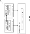
- FIG. 1 is a block diagram of an embodiment of a system 100 comprising a multi-cluster heterogeneous processor architecture.
- the system 100 may be implemented in any computing device, including a personal computer, a workstation, a server, a portable computing device (PCD), such as a cellular telephone, a portable digital assistant (PDA), a portable game console, a palmtop computer, or a tablet computer.
- the multi-cluster heterogeneous processor architecture comprises a plurality of processor clusters coupled to a cache controller 101.
- each processor cluster may comprise one or more processors or processor cores (e.g ., central processing unit (CPU), graphics processing unit (GPU), digital signal processor (DSP), etc .) with a corresponding dedicated cache.
- CPU central processing unit
- GPU graphics processing unit
- DSP digital signal processor
- the processor clusters 102 and 104 may comprise a "big.LITTLE" heterogeneous architecture, as described above, in which the processor cluster 102 comprises a Little cluster and the processor cluster 104 comprises a Big cluster.
- the Little processor cluster 102 comprises a plurality of central processing unit (CPU) cores 108 and 110 which are relatively slower and consume less power than the CPU cores 114 and 116 in the Big processor cluster 104.
- the Big cluster CPU cores 114 and 116 may be distinguished from the Little cluster CPU cores 108 and 110 by, for example, a relatively higher instructions per cycle (IPC), higher operating frequency, and/or having a micro-architectural feature that enables relatively more performance but at the cost of additional power.
- additional processor clusters may be included in the system 100, such as, for example, a processor cluster 106 comprising GPU cores 120 and 122.
- Processor clusters 102, 104, and 106 may have independent cache memory used by the corresponding processors in the system 100 to reduce the average time to access data from a main memory 144.
- the independent cache memory and the main memory 144 may be organized as a hierarchy of cache levels (e.g., level one (L1), level two (L2), level three (L3).
- Processor cluster 102 may comprise L2 cache 112
- processor cluster 104 may comprise L2 cache 118
- processor cluster 106 may comprise L2 cache 124.
- the cache controller 101 may comprise a cache scheduler 140, a cache interconnect 111, and a plurality of cache monitors 126, 128, and 130 for monitoring the performance of L2 cache 112, 118, and 124, respectively.
- Cache interconnect 111 comprises an interconnect or bus with associated logic for maintaining coherency between main memory 144 and L2 cache 112, 118, and 124.
- the cache scheduler 140 generally comprises logic configured to monitor processor and cache performance and optimally manage task scheduling to the processor clusters 101, 104, and 106 according to power and performance requirements of the system 100.
- FIG. 2 is a block diagram illustrating the data inputs and outputs of an embodiment of the cache scheduler 140.
- the cache scheduler 140 may receive as data inputs, from each processor cluster, processor usage input data 202 and L2 cache usage/miss rate input data 204.
- processor usage input data 202 may indicate processor workload based on one or more of the following or other parameters received from processor clusters 102, 104, and 106: instructions per cycle (IPC), million instructions per second (MIPS), frequency, CPU active duration percentage.
- L2 cache input data 204 may indicate L2 cache workload or performance based on one or more of the following or other parameters received via cache monitors 126, 128, and 130: cache misses per 1000 instructions (MPKI), cache accesses per 1000 instructions (APKI), L2 cache miss rate (MPKI/APKI), CPU stall time/ratio or stall clocks due to cache misses, and million cycles per second (MCPS) indicating an amount of CPU stalls due to cache misses.
- MPKI cache misses per 1000 instructions
- APKI cache accesses per 1000 instructions
- MPKI/APKI L2 cache miss rate
- CPU stall time/ratio or stall clocks due to cache misses CPU stall time/ratio or stall clocks due to cache misses
- MCPS million cycles per second
- the cache scheduler 140 determines whether a processing bottleneck or other system limitation is being (or will be) caused by (1) processor/CPU performance or (2) the size of the L2 cache. For example, the cache scheduler 140 may determine that a current task associated with the Little processor cluster 102 is limited by CPU performance.
- the processor usage input data 202 may indicate that the CPU workload is more than can be desirably handled by the Little processor cluster 102.
- cache scheduler 140 may initiate a task migration mode 208 for migrating the task to from the Little processor cluster 102 to the Big processor cluster 104 where it can be executed by CPU 114 or CPU 116 with more desirable performance than available via CPU 108 or CPU 100.
- the cache scheduler 140 may determine that the current task associated with the Little processor cluster 102 is limited by the size of the L2 cache 112.
- the input data 204 may indicate that the size of L2 cache 112 is the limitation (not CPU performance).
- the cache scheduler 140 may initiate a cache extension mode 206 for processing the task via the Little processor cluster 102 but by using a portion of L2 cache 118 (in Big processor cluster 104) as an extended L2 cache or L3 cache. If there arc no performance issues with the current task, then the cache scheduler 140 may initiate a default split L2 mode 210 for keeping the current task with L2 cache 112 of the Little processor cluster 102.
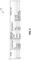
- the cache scheduler 140 may access and manage a table 300 for determining whether to initiate cache extension mode 206, task migration mode 208, or the default split L2 mode 210.
- the table 300 may define a cache size threshold (threshold 2) and a performance threshold (threshold 1).
- the cache scheduler 140 may determine four exemplary scenarios. In scenario 4, the cache scheduler 140 may initiate the cache extension mode 206 when the Little processor cluster 102 has a CPU usage percentage that docs not exceed threshold 1 but an L2 cache usage/miss rate exceeds threshold 2.
- the cache scheduler 140 may initiate the task migration mode 208 when the Little processor cluster 102 has a CPU usage percentage that exceeds threshold 1 regardless of the L2 cache usage/miss rate.
- the cache scheduler 140 may initiate the default split L2 mode 210 when the Little processor cluster 102 has a CPU usage percentage that does not exceed threshold 1 and an L2 cache usage/miss rate does not exceed threshold 2.
- Scenario 1 refers to the situation in which the Big processor cluster 104 is actively handling tasks and the system 100 operates in the default split L2 mode 210 for the Big processor cluster 104.
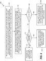
- FIG. 4 is a flowchart illustrating an embodiment of a method 400 implemented by the cache scheduler 140.
- the cache scheduler 140 receives a processor workload input and a cache workload input for the Little processor cluster 102 and associated L2 cache 112.
- the processor and cache workload inputs may comprise any of the parameters mentioned above (inputs 202 and 204 - FIG. 2 ).
- the cache scheduler 140 determines whether a current task associated with the Little processor cluster 102 is limited by a size threshold of L2 cache 112 or a performance threshold of CPU 108 or CPU 110.
- the performance and size thresholds may be defined in a manner similar to table 300 in FIG. 3 . It should be appreciated that the thresholds may be programmatically defined or otherwise.
- the cache scheduler 140 may use at least a portion of L2 cache 118 associated with the Big processor cluster 104 as an extension of L2 cache 112 (block 408).
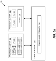
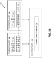
- FIGS 5a - 5c illustrate in schematic form two exemplary embodiments for dynamically extending L2 cache 112.
- a current task may be associated with CPU 108 in the Little processor cluster 102.
- CPU 108 and L2 cache 1 12 are highlighted as grayed-out boxes.
- a portion 502 of L2 cache 118 (Big processor cluster 104) may be allocated as extended L2 cache for L2 cache 112 (Little processor cluster 102).
- FIG. 5c illustrates another embodiment in which a portion 504 of L2 cache 118 (Big processor cluster 104) is allocated as L3 cache used by L2 cache 112 (Little processor cluster 102). It should be appreciated that various cache techniques may be employed depending the hierarchy of cache levels implemented in system 100.
- FIG. 6 illustrates an exemplary mapping of a physical cache 602 to a logical cache 604 for implementing the dynamic cache extension module 150.
- Physical cache 602 may be allocated as follows.
- a processor cluster A may comprise physical cache portions A1 and A2 in L2 cache A.
- a processor cluster B may comprise physical cache portions B1, B2, B3, and B4 in L2 cache B.
- a processor cluster C may comprise physical cache portions C1, C2, and C3 in L2 cache C.
- the cache scheduler 140 may allocate physical cache portions B1, B2, and B3 from L2 cache B (processor cluster B) to L2 cache A (processor cluster A).
- Physical cache portion B from cache B (processor cluster B) may be allocated to L2 cache C (processor cluster C).
- the processor cluster B may be inactivated and power collapsed to conserve power consumption.
- FIG. 7 illustrates a mapping table 700 for implementing the physical-to-logical cache mapping of FIG. 6 .
- FIGS. 8a & 8b illustrate in schematic form an exemplary task migration.
- a current task 802 is associated with CPU 110 in Little processor cluster 102.
- the cache scheduler 140 may migrate task 802 from CPU 110 to CPU 114.
- L2 cache 118 in Big processor cluster 104 may fetch all of its working set from L2 cache 112 in Little processor cluster 102.
- L2 cache 118 may fetch a portion of its working set from L2 cache 112 in Little processor cluster 102 while it fetches a fresh set from main memory 144 or a lower level cache ( e.g. , L3 cache).
- a source L2 cache may be defined as the L2 cache from which an executed thread is migrating away.
- the cache scheduler 140 may be further configured to keep the source L2 cache online as long as a threshold cache hit ratio is maintained from the source L2 cache.
- the source L2 cache may be flushed and turned off when the hit ratio falls below the threshold cache hit ratio.
- the system 100 may be configured to tune the threshold cache hit ratio to optimize performance and/or power.
- a scheduler 907 and low power mode driver(s) 901 may be implemented in software, and the timeout selection algorithm 903 may be implemented in hardware.
- a scheduler 907 may receive task wakeup inputs 902 and determine whether task migration should be performed (decision block 904) as described above in more detail. If the scheduler 907 determines that task migration is not to be performed, at block 906, the task may be scheduled on the original processor cluster. If task migration is desired, at block 908, the task may be migrated to a destination processor cluster.
- the tuning/timeout technique is represented by steps A, B, C, D, and E in FIG. 9 .
- task migration may trigger a control signal to, for example, low power mode driver(s) 901.
- the low power mode driver 901 determines whether the core(s) in the source processor should be collapsed. If the source L2 cache 909 can collapse (decision block 910), at step B, a collapse timeout and a snoot hit threshold may be set. The collapse timeout may be set (block 920) based on the recommended timeout received (step C) by the timeout selection algorithm 903.
- the snoop hit threshold and the snoop hit timeout may be stored in the source L2 cache 903 at blocks 922 and 924, respectively.
- the source L2 cache 909 may be collapsed (block 928) in response to a timeout IRQ line based on the snoot hit threshold, a snoop hit counter, and the snoop hit timeout.
- FIG. 10 illustrates the system 100 incorporated in an exemplary portable computing device (PCD) 1000.
- a system-on-chip (SoC) 103 may include the cache scheduler 140 and the processor clusters 102, 104, and 106.
- a display controller 328 and a touch scrccn controller 1006 may be coupled to one or more of the processor clusters.
- the touch screen display 1006 external to the on-chip system 103 may be coupled to the display controller 328 and the touch screen controller 330.
- FIG. 10 further shows that a video encoder 334, e.g., a phase alternating line (PAL) encoder, a sequential color a memoire (SECAM) encoder, or a national television system(s) committee (NTSC) encoder, is coupled to one or more of the processor clusters 102, 104, and 106.
- a video amplifier 336 is coupled to the video encoder 334 and the touch screen display 1006.
- a video port 338 is coupled to the video amplifier 336.
- a universal serial bus (USB) controller 340 is coupled to one or more of the processor clusters.
- a USB port 342 is coupled to the USB controller 340.
- Memory 144 and a subscriber identity module (STM) card 346 may also be coupled to the processor cluster(s).
- STM subscriber identity module
- a digital camera 348 may be coupled to the processor cluster(s).
- the digital camera 348 is a charge-coupled device (CCD) camera or a complementary metal-oxide semiconductor (CMOS) camera.
- CCD charge-coupled device
- CMOS complementary metal-oxide semiconductor
- a stereo audio coder-decoder (CODEC) 350 may be coupled to the processor cluster(s). Moreover, an audio amplifier 352 may coupled to the stereo audio CODEC 350. In an exemplary aspect, a first stereo speaker 354 and a second stereo speaker 356 are coupled to the audio amplifier 352. A microphone amplifier 358 may be also coupled to the stereo audio CODEC 350. Additionally, a microphone 360 may be coupled to the microphone amplifier 358. In a particular aspect, a frequency modulation (FM) radio tuner 362 may be coupled to the stereo audio CODEC 350. Also, an FM antenna 364 is coupled to the FM radio tuner 362. Further, stereo headphones 366 may be coupled to the stereo audio CODEC 350.
- FM frequency modulation
- FIG. 10 further illustrates that a radio frequency (RF) transceiver 368 may be coupled to the processor cluster(s).
- An RF switch 370 may be coupled to the RF transceiver 368 and an RF antenna 372.
- a keypad 204, a mono headset with a microphone 376, and a vibrator device 378 may be coupled to the processor cluster(s).
- FIG. 10 also shows that a power supply 380 may be coupled to the on-chip system 103.
- the power supply 380 is a direct current (DC) power supply that provides power to the various components of the PCD 1000 that require power.
- the power supply is a rechargeable DC battery or a DC power supply that is derived from an alternating current (AC) to DC transformer that is connected to an AC power source.
- DC direct current
- FIG. 10 further indicates that the PCD 1000 may also include a network card 388 that may be used to access a data network, e.g., a local area network, a personal area network, or any other network.
- the network card 388 may be a Bluetooth network card, a WiFi network card, a personal area network (PAN) card, a personal area network ultra-low-power technology (PeANUT) network card, a television/cable/satellite tuner, or any other network card well known in the art.
- the network card 388 may be incorporated into a chip, i.e., the network card 388 may be a full solution in a chip, and may not be a separate network card 388.
- the memory 144, the RAM card 105, touch screen display 1006, the video port 338, the USB port 342, the camera 348, the first stereo speaker 354, the second stereo speaker 356, the microphone 360, the FM antenna 364, the stereo headphones 366, the RF switch 370, the RF antenna 372, the keypad 374, the mono headset 376, the vibrator 378, and the power supply 380 may be external to the on-chip system 103.
- the functions described may be implemented in hardware, software, firmware, or any combination thereof. If implemented in software, the functions may be stored on or transmitted as one or more instructions or code on a computer-readable medium.
- Computer-readable media include both computer storage media and communication media including any medium that facilitates transfer of a computer program from one place to another.
- a storage media may be any available media that may be accessed by a computer.
- such computer-readable media may comprise RAM, ROM, EEPROM, NAND flash, NOR flash, M-RAM, P-RAM, R-RAM, CD-ROM or other optical disk storage, magnetic disk storage or other magnetic storage devices, or any other medium that may be used to carry or store desired program code in the form of instructions or data structures and that may be accessed by a computer.
- any connection is properly termed a computer-readable medium.
- the software is transmitted from a website, server, or other remote source using a coaxial cable, fiber optic cable, twisted pair, digital subscriber line ("DSL"), or wireless technologies such as infrared, radio, and microwave
- coaxial cable, fiber optic cable, twisted pair, DSL, or wireless technologies such as infrared, radio, and microwave are included in the definition of medium.
- Disk and disc includes compact disc (“CD”), laser disc, optical disc, digital versatile disc (“DVD”), floppy disk and blu-ray disc where disks usually reproduce data magnetically, while discs reproduce data optically with lasers. Combinations of the above should also be included within the scope of computer-readable media.
Landscapes
- Engineering & Computer Science (AREA)
- Theoretical Computer Science (AREA)
- General Engineering & Computer Science (AREA)
- Physics & Mathematics (AREA)
- General Physics & Mathematics (AREA)
- Software Systems (AREA)
- Computer Hardware Design (AREA)
- Quality & Reliability (AREA)
- Memory System Of A Hierarchy Structure (AREA)
Description
- Portable computing devices (e.g., cellular telephones, smart phones, tablet computers, portable digital assistants (PDAs), and portable game consoles) continue to offer an ever-expanding array of features and services, and provide users with unprecedented levels of access to information, resources, and communications. To keep pace with these service enhancements, such devices have become more powerful and more complex. Portable computing devices now commonly include a system on chip (SoC) comprising one or more chip components embedded on a single substrate (e.g., one or more central processing units (CPUs), a graphics processing unit (GPU), digital signal processors, etc.).
- Such portable computing devices or other computer systems or devices may comprise a multi-cluster heterogeneous processor architecture, an example of which is referred to as a "big.LITTLE" heterogeneous architecture. The "big.LITTLE" and other heterogeneous architectures typically comprise a group of processor cores in which a set of relatively slower, lower-power processor cores arc coupled with a set of relatively more powerful processor cores. For example, a set of processors or processor cores with a higher performance ability are often referred to as the "Big cluster" while the other set of processors or processor cores with minimum power consumption yet capable of delivering appropriate performance (but relatively less than that of the Big cluster) is referred to as the "Little cluster." A cache controller may schedule tasks to be performed by the Big cluster or the Little cluster according to performance and/or power requirements, which may vary based on various use cases. The Big cluster may be used for situations in which higher performance is desirable (e.g., graphics, gaming, etc.), and the Little cluster may be used for relatively lower power user cases (e.g., text applications).
- Existing multi-cluster heterogeneous processor architectures, however, may not effectively optimize performance/power in certain use cases. For instance, use cases with wide memory access but relatively light CPU workload may experience undesirable level two (L2) cache misses. Existing architectures may interpret this type of use case/workload as a relatively heavy CPU workload due to execution latency. As a result, if a task gets migrated to the Big cluster, the system may experience a power penalty. Alternatively, if the task is left running on the Little cluster, performance may suffer. Furthermore, if the scheduler migrates tasks from a Little cluster having a smaller size L2 cache to a Big cluster having a larger L2 cache, the system may consume excessive power. If the scheduler keeps tasks in the Little with the smaller size L2 cache, then this may result in low performance and an undesirable user experience.
- The article "CloudCache: Expanding and Shrinking Private Caches" of Hyunjin Lee, proceedings of the international symposium on high-performance computer architecture, ISBN 978-1-4244-9432-3, proposes CloudCache, a distributed L2 cache substrate for many-core chip multi-processors. CloudCache creates dynamically expending and shrinking L2 caches for working threats with fine-grained hardware monitoring and control.
- Accordingly, there is a need in the art for systems and methods for scheduling and managing tasks in multi-cluster heterogeneous processor architectures with optimized performance and power consumption.
- Various embodiments of methods, systems, and computer programs are disclosed for providing dynamic cache extension in a multi-cluster heterogeneous processor architecture in a portable computing device. One such method involves receiving a processor workload input and a cache workload input for a first processor cluster and an associated first cache in a multi-cluster heterogeneous processor architecture comprising the first processor cluster and a second processor cluster having an associated second cache. Based on the processor workload input and the cache workload input, it is determined whether a current task associated with the first processor cluster is limited by a size threshold of the first cache or a performance threshold of the first processor cluster. If the current task is limited by the size threshold of the first cache, at least a portion of the second cache associated with the second processor cluster may be used as an extension of the first cache.
- Another embodiment is a system having a multi-cluster heterogeneous processor architecture for providing dynamic cache extension. The system comprises a first processor cluster comprising a first level 2 (L2) cache, and a second processor cluster comprising a second L2 cache. A cache controller in communication with the first and second L2 caches is configured to receive a processor workload input and a cache workload input from the first processor cluster. Based on the processor workload input and the cache workload input, the cache controller may determine whether a current task associated with the first processor cluster is limited by a size threshold of the first L2 cache or a performance threshold of the first processor cluster. If the current task is limited by the size threshold of the first L2 cache, the cache controller may use at least a portion of the second L2 cache associated with the second processor cluster as an extension of the first L2 cache.
- In the Figures, like reference numerals refer to like parts throughout the various views unless otherwise indicated. For reference numerals with letter character designations such as "102A" or "102B", the letter character designations may differentiate two like parts or elements present in the same Figure. Letter character designations for reference numerals may be omitted when it is intended that a reference numeral to encompass all parts having the same reference numeral in all Figures.
-
FIG. 1 is a block diagram of an embodiment of a system comprising a multi-cluster heterogeneous processor architecture that includes a cache scheduler for providing dynamic cache extension and dynamic cache reallocation between processor clusters. -
FIG. 2 is a block diagram illustrating the data inputs and outputs of an embodiment of the cache scheduler in the system ofFIG. 1 . -
FIG. 3 is a data table illustrating exemplary data inputs and resulting data outputs of the cache scheduler inFIG. 2 . -
FIG. 4 is a flowchart illustrating an embodiment of a method implemented by the cache scheduler for providing dynamic cache extension and dynamic cache reallocation. -
FIG. 5a is a functional block diagram illustrating an embodiment of the system ofFIG. 1 for implementing dynamic cache extension. -
FIG. 5b illustrates the system ofFIG. 5a in which the L2 cache of one processor cluster is extended by using a portion of the L2 cache of another processor cluster as additional L2 cache. -
FIG. 5c illustrates the system ofFIG. 5a in which the L2 cache of one processor cluster is extended by using a portion of the L2 cache of another processor cluster as an L3 cache. -
FIG. 6 is a block diagram illustrating a physical-to-logical cache mapping for implementing dynamic cache extension. -
FIG. 7 is an embodiment of a look-up table managed by the cache controller for implementing the physical-to-logical mapping ofFIG. 6 -
FIG. 8a is a functional block diagram illustrating an embodiment of the system ofFIG. 1 for implementing dynamic cache reallocation. -
FIG. 8b illustrates the system ofFIG. 8a in which a task is reallocated from one processor cluster to another processor cluster. -
FIG. 9 illustrates another embodiment of the system ofFIG. 1 for collapsing a source L2 cache after a task has been migrated to a destination L2 cache in another processor cluster based on a snoop hit counter. -
FIG. 10 illustrates the systems and methods ofFIGS. 1 - 9 incorporated in an exemplary portable computing device (PCD). - The word "exemplary" is used herein to mean "serving as an example, instance, or illustration." Any aspect described herein as "exemplary" is not necessarily to be construed as preferred or advantageous over other aspects.
- In this description, the term "application" or "image" may also include files having executable content, such as: object code, scripts, byte code, markup language files, and patches. In addition, an "application" referred to herein, may also include files that are not executable in nature, such as documents that may need to be opened or other data files that need to be accessed.
- The term "content" may also include files having executable content, such as: object code, scripts, byte code, markup language files, and patches. In addition, "content" referred to herein, may also include files that are not executable in nature, such as documents that may need to be opened or other data files that need to be accessed.
- As used in this description, the terms "component," "database," "module," "system," and the like are intended to refer to a computer-related entity, either hardware, firmware, a combination of hardware and software, software, or software in execution. For example, a component may be, but is not limited to being, a process running on a processor, a processor, an object, an executable, a thread of execution, a program, and/or a computer. By way of illustration, both an application running on a computing device and the computing device may be a component. One or more components may reside within a process and/or thread of execution, and a component may be localized on one computer and/or distributed between two or more computers. In addition, these components may execute from various computer readable media having various data structures stored thereon. The components may communicate by way of local and/or remote processes such as in accordance with a signal having one or more data packets (e.g., data from one component interacting with another component in a local system, distributed system, and/or across a network such as the Internet with other systems by way of the signal).
-
FIG. 1 is a block diagram of an embodiment of asystem 100 comprising a multi-cluster heterogeneous processor architecture. Thesystem 100 may be implemented in any computing device, including a personal computer, a workstation, a server, a portable computing device (PCD), such as a cellular telephone, a portable digital assistant (PDA), a portable game console, a palmtop computer, or a tablet computer. The multi-cluster heterogeneous processor architecture comprises a plurality of processor clusters coupled to acache controller 101. As known in the art, each processor cluster may comprise one or more processors or processor cores (e.g., central processing unit (CPU), graphics processing unit (GPU), digital signal processor (DSP), etc.) with a corresponding dedicated cache. - In the embodiment of
FIG. 1 , theprocessor clusters processor cluster 102 comprises a Little cluster and theprocessor cluster 104 comprises a Big cluster. TheLittle processor cluster 102 comprises a plurality of central processing unit (CPU)cores CPU cores Big processor cluster 104. It should be appreciated that the Bigcluster CPU cores cluster CPU cores system 100, such as, for example, aprocessor cluster 106 comprisingGPU cores -
Processor clusters system 100 to reduce the average time to access data from amain memory 144. In an embodiment, the independent cache memory and themain memory 144 may be organized as a hierarchy of cache levels (e.g., level one (L1), level two (L2), level three (L3).Processor cluster 102 may compriseL2 cache 112,processor cluster 104 may compriseL2 cache 118, andprocessor cluster 106 may compriseL2 cache 124. - As illustrated in
FIG. 1 , thecache controller 101 may comprise acache scheduler 140, acache interconnect 111, and a plurality of cache monitors 126, 128, and 130 for monitoring the performance ofL2 cache Cache interconnect 111 comprises an interconnect or bus with associated logic for maintaining coherency betweenmain memory 144 andL2 cache cache scheduler 140 generally comprises logic configured to monitor processor and cache performance and optimally manage task scheduling to theprocessor clusters system 100. -
FIG. 2 is a block diagram illustrating the data inputs and outputs of an embodiment of thecache scheduler 140. Thecache scheduler 140 may receive as data inputs, from each processor cluster, processor usage input data 202 and L2 cache usage/missrate input data 204. It should be appreciated that processor usage input data 202 may indicate processor workload based on one or more of the following or other parameters received fromprocessor clusters cache input data 204 may indicate L2 cache workload or performance based on one or more of the following or other parameters received via cache monitors 126, 128, and 130: cache misses per 1000 instructions (MPKI), cache accesses per 1000 instructions (APKI), L2 cache miss rate (MPKI/APKI), CPU stall time/ratio or stall clocks due to cache misses, and million cycles per second (MCPS) indicating an amount of CPU stalls due to cache misses. - Based on the
input data 202 and 204, thecache scheduler 140 determines whether a processing bottleneck or other system limitation is being (or will be) caused by (1) processor/CPU performance or (2) the size of the L2 cache. For example, thecache scheduler 140 may determine that a current task associated with theLittle processor cluster 102 is limited by CPU performance. The processor usage input data 202 may indicate that the CPU workload is more than can be desirably handled by theLittle processor cluster 102. In response, cache scheduler 140 (e.g., dynamic cache reallocation module(s) 152), may initiate atask migration mode 208 for migrating the task to from theLittle processor cluster 102 to theBig processor cluster 104 where it can be executed byCPU 114 orCPU 116 with more desirable performance than available viaCPU 108 orCPU 100. Alternatively, thecache scheduler 140 may determine that the current task associated with theLittle processor cluster 102 is limited by the size of theL2 cache 112. Theinput data 204 may indicate that the size ofL2 cache 112 is the limitation (not CPU performance). In response, the cache scheduler 140 (e.g., dynamic cache extension module(s) 150) may initiate acache extension mode 206 for processing the task via theLittle processor cluster 102 but by using a portion of L2 cache 118 (in Big processor cluster 104) as an extended L2 cache or L3 cache. If there arc no performance issues with the current task, then thecache scheduler 140 may initiate a defaultsplit L2 mode 210 for keeping the current task withL2 cache 112 of theLittle processor cluster 102. - As illustrated in
FIG. 3 , thecache scheduler 140 may access and manage a table 300 for determining whether to initiatecache extension mode 206,task migration mode 208, or the defaultsplit L2 mode 210. The table 300 may define a cache size threshold (threshold 2) and a performance threshold (threshold 1). Based on thedata inputs 202 and 204, thecache scheduler 140 may determine four exemplary scenarios. Inscenario 4, thecache scheduler 140 may initiate thecache extension mode 206 when theLittle processor cluster 102 has a CPU usage percentage that docs not exceedthreshold 1 but an L2 cache usage/miss rate exceedsthreshold 2. Inscenario 3, thecache scheduler 140 may initiate thetask migration mode 208 when theLittle processor cluster 102 has a CPU usage percentage that exceedsthreshold 1 regardless of the L2 cache usage/miss rate. Inscenario 2, thecache scheduler 140 may initiate the defaultsplit L2 mode 210 when theLittle processor cluster 102 has a CPU usage percentage that does not exceedthreshold 1 and an L2 cache usage/miss rate does not exceedthreshold 2.Scenario 1 refers to the situation in which theBig processor cluster 104 is actively handling tasks and thesystem 100 operates in the defaultsplit L2 mode 210 for theBig processor cluster 104. -
FIG. 4 is a flowchart illustrating an embodiment of amethod 400 implemented by thecache scheduler 140. Atblock 402, thecache scheduler 140 receives a processor workload input and a cache workload input for theLittle processor cluster 102 and associatedL2 cache 112. The processor and cache workload inputs may comprise any of the parameters mentioned above (inputs 202 and 204 -FIG. 2 ). Atblock 404, thecache scheduler 140 determines whether a current task associated with theLittle processor cluster 102 is limited by a size threshold ofL2 cache 112 or a performance threshold ofCPU 108 orCPU 110. The performance and size thresholds may be defined in a manner similar to table 300 inFIG. 3 . It should be appreciated that the thresholds may be programmatically defined or otherwise. If thecache scheduler 140 determines that the current task is limited by the size threshold of L2 cache 112 (decision block 406), thecache scheduler 140 may use at least a portion ofL2 cache 118 associated with theBig processor cluster 104 as an extension of L2 cache 112 (block 408). -
FIGS 5a - 5c illustrate in schematic form two exemplary embodiments for dynamically extendingL2 cache 112. As illustrated inFIG. 5a , a current task may be associated withCPU 108 in theLittle processor cluster 102.CPU 108 andL2 cache 1 12 are highlighted as grayed-out boxes. InFIG. 5b , aportion 502 of L2 cache 118 (Big processor cluster 104) may be allocated as extended L2 cache for L2 cache 112 (Little processor cluster 102).FIG. 5c illustrates another embodiment in which aportion 504 of L2 cache 118 (Big processor cluster 104) is allocated as L3 cache used by L2 cache 112 (Little processor cluster 102). It should be appreciated that various cache techniques may be employed depending the hierarchy of cache levels implemented insystem 100. -
FIG. 6 illustrates an exemplary mapping of aphysical cache 602 to alogical cache 604 for implementing the dynamiccache extension module 150.Physical cache 602 may be allocated as follows. A processor cluster A may comprise physical cache portions A1 and A2 in L2 cache A. A processor cluster B may comprise physical cache portions B1, B2, B3, and B4 in L2 cache B. A processor cluster C may comprise physical cache portions C1, C2, and C3 in L2 cache C. In operation and based on thedata inputs 202 and 204, thecache scheduler 140 may allocate physical cache portions B1, B2, and B3 from L2 cache B (processor cluster B) to L2 cache A (processor cluster A). Physical cache portion B from cache B (processor cluster B) may be allocated to L2 cache C (processor cluster C). In this operational use case, the processor cluster B may be inactivated and power collapsed to conserve power consumption.FIG. 7 illustrates a mapping table 700 for implementing the physical-to-logical cache mapping ofFIG. 6 . - Referring again to
FIG. 4 , if thecache scheduler 140 determines that the current task is not limited by the size threshold of L2 cache 112 (decision block 406), control may flow to decision block 410 to determine if the current task is limited by the performance threshold of theL2 cache 112. If the performance threshold is not exceeded, thecache scheduler 140 may process the current task using the default L2 split mode 210 (block 412). If the performance threshold is exceeded, the cache scheduler may migrate the current task from theLittle processor cluster 102 to the Big processor cluster 104 (block 414).FIGS. 8a &8b illustrate in schematic form an exemplary task migration. InFIG. 8a , acurrent task 802 is associated withCPU 110 inLittle processor cluster 102. As illustrated inFIG. 8b , if the performance threshold is exceeded, thecache scheduler 140 may migratetask 802 fromCPU 110 toCPU 114. - According to another exemplary embodiment of the
system 100, when a task is migrated from theLittle processor cluster 102 to theBig processor cluster 104,L2 cache 118 inBig processor cluster 104 may fetch all of its working set fromL2 cache 112 inLittle processor cluster 102. Alternatively,L2 cache 118 may fetch a portion of its working set fromL2 cache 112 inLittle processor cluster 102 while it fetches a fresh set frommain memory 144 or a lower level cache (e.g., L3 cache). In this regard, a source L2 cache may be defined as the L2 cache from which an executed thread is migrating away. Thecache scheduler 140 may be further configured to keep the source L2 cache online as long as a threshold cache hit ratio is maintained from the source L2 cache. The source L2 cache may be flushed and turned off when the hit ratio falls below the threshold cache hit ratio. - As illustrated in
FIG. 9 , thesystem 100 may be configured to tune the threshold cache hit ratio to optimize performance and/or power. In an embodiment, ascheduler 907 and low power mode driver(s) 901 may be implemented in software, and thetimeout selection algorithm 903 may be implemented in hardware. For example, consider the situation in which anoperating system 905 frequently performs task migrations. Ascheduler 907 may receivetask wakeup inputs 902 and determine whether task migration should be performed (decision block 904) as described above in more detail. If thescheduler 907 determines that task migration is not to be performed, atblock 906, the task may be scheduled on the original processor cluster. If task migration is desired, atblock 908, the task may be migrated to a destination processor cluster. - In an exemplary embodiment, the tuning/timeout technique is represented by steps A, B, C, D, and E in
FIG. 9 . At step A, task migration may trigger a control signal to, for example, low power mode driver(s) 901. Atblock 910, the lowpower mode driver 901 determines whether the core(s) in the source processor should be collapsed. If thesource L2 cache 909 can collapse (decision block 910), at step B, a collapse timeout and a snoot hit threshold may be set. The collapse timeout may be set (block 920) based on the recommended timeout received (step C) by thetimeout selection algorithm 903. At step D, the snoop hit threshold and the snoop hit timeout may be stored in thesource L2 cache 903 atblocks source L2 cache 909 may be collapsed (block 928) in response to a timeout IRQ line based on the snoot hit threshold, a snoop hit counter, and the snoop hit timeout. - The
system 100 may be incorporated into any desirable computing system.FIG. 10 illustrates thesystem 100 incorporated in an exemplary portable computing device (PCD) 1000. A system-on-chip (SoC) 103 may include thecache scheduler 140 and theprocessor clusters display controller 328 and atouch scrccn controller 1006 may be coupled to one or more of the processor clusters. In turn, thetouch screen display 1006 external to the on-chip system 103 may be coupled to thedisplay controller 328 and thetouch screen controller 330. -
FIG. 10 further shows that avideo encoder 334, e.g., a phase alternating line (PAL) encoder, a sequential color a memoire (SECAM) encoder, or a national television system(s) committee (NTSC) encoder, is coupled to one or more of theprocessor clusters video amplifier 336 is coupled to thevideo encoder 334 and thetouch screen display 1006. Also, avideo port 338 is coupled to thevideo amplifier 336. As shown inFIG. 10 , a universal serial bus (USB)controller 340 is coupled to one or more of the processor clusters. Also, aUSB port 342 is coupled to theUSB controller 340.Memory 144 and a subscriber identity module (STM) card 346 may also be coupled to the processor cluster(s). - Further, as shown in
FIG. 10 , adigital camera 348 may be coupled to the processor cluster(s). In an exemplary aspect, thedigital camera 348 is a charge-coupled device (CCD) camera or a complementary metal-oxide semiconductor (CMOS) camera. - As further illustrated in
FIG. 10 , a stereo audio coder-decoder (CODEC) 350 may be coupled to the processor cluster(s). Moreover, anaudio amplifier 352 may coupled to thestereo audio CODEC 350. In an exemplary aspect, afirst stereo speaker 354 and asecond stereo speaker 356 are coupled to theaudio amplifier 352. Amicrophone amplifier 358 may be also coupled to thestereo audio CODEC 350. Additionally, amicrophone 360 may be coupled to themicrophone amplifier 358. In a particular aspect, a frequency modulation (FM)radio tuner 362 may be coupled to thestereo audio CODEC 350. Also, anFM antenna 364 is coupled to theFM radio tuner 362. Further,stereo headphones 366 may be coupled to thestereo audio CODEC 350. -
FIG. 10 further illustrates that a radio frequency (RF)transceiver 368 may be coupled to the processor cluster(s). AnRF switch 370 may be coupled to theRF transceiver 368 and an RF antenna 372. Akeypad 204, a mono headset with amicrophone 376, and avibrator device 378 may be coupled to the processor cluster(s). -
FIG. 10 also shows that apower supply 380 may be coupled to the on-chip system 103. In a particular aspect, thepower supply 380 is a direct current (DC) power supply that provides power to the various components of thePCD 1000 that require power. Further, in a particular aspect, the power supply is a rechargeable DC battery or a DC power supply that is derived from an alternating current (AC) to DC transformer that is connected to an AC power source. -
FIG. 10 further indicates that thePCD 1000 may also include anetwork card 388 that may be used to access a data network, e.g., a local area network, a personal area network, or any other network. Thenetwork card 388 may be a Bluetooth network card, a WiFi network card, a personal area network (PAN) card, a personal area network ultra-low-power technology (PeANUT) network card, a television/cable/satellite tuner, or any other network card well known in the art. Further, thenetwork card 388 may be incorporated into a chip, i.e., thenetwork card 388 may be a full solution in a chip, and may not be aseparate network card 388. - Referring to
FIG. 10 , it should be appreciated that thememory 144, the RAM card 105,touch screen display 1006, thevideo port 338, theUSB port 342, thecamera 348, thefirst stereo speaker 354, thesecond stereo speaker 356, themicrophone 360, theFM antenna 364, thestereo headphones 366, theRF switch 370, the RF antenna 372, the keypad 374, themono headset 376, thevibrator 378, and thepower supply 380 may be external to the on-chip system 103. - Certain steps in the processes or process flows described in this specification naturally precede others for the invention to function as described. However, the invention is not limited to the order of the steps described if such order or sequence does not alter the functionality of the invention. That is, it is recognized that some steps may performed before, after, or parallel (substantially simultaneously with) other steps without departing from the scope of the invention. In some instances, certain steps may be omitted or not performed without departing from the invention. Further, words such as "thereafter", "then", "next", etc. are not intended to limit the order of the steps. These words are simply used to guide the reader through the description of the exemplary method.
- Additionally, one of ordinary skill in programming is able to write computer code or identify appropriate hardware and/or circuits to implement the disclosed invention without difficulty based on the flow charts and associated description in this specification, for example.
- Therefore, disclosure of a particular set of program code instructions or detailed hardware devices is not considered necessary for an adequate understanding of how to make and use the invention. The inventive functionality of the claimed computer implemented processes is explained in more detail in the above description and in conjunction with the Figures which may illustrate various process flows.
- In one or more exemplary aspects, the functions described may be implemented in hardware, software, firmware, or any combination thereof. If implemented in software, the functions may be stored on or transmitted as one or more instructions or code on a computer-readable medium. Computer-readable media include both computer storage media and communication media including any medium that facilitates transfer of a computer program from one place to another. A storage media may be any available media that may be accessed by a computer. By way of example, and not limitation, such computer-readable media may comprise RAM, ROM, EEPROM, NAND flash, NOR flash, M-RAM, P-RAM, R-RAM, CD-ROM or other optical disk storage, magnetic disk storage or other magnetic storage devices, or any other medium that may be used to carry or store desired program code in the form of instructions or data structures and that may be accessed by a computer.
- Also, any connection is properly termed a computer-readable medium. For example, if the software is transmitted from a website, server, or other remote source using a coaxial cable, fiber optic cable, twisted pair, digital subscriber line ("DSL"), or wireless technologies such as infrared, radio, and microwave, then the coaxial cable, fiber optic cable, twisted pair, DSL, or wireless technologies such as infrared, radio, and microwave are included in the definition of medium.
- Disk and disc, as used herein, includes compact disc ("CD"), laser disc, optical disc, digital versatile disc ("DVD"), floppy disk and blu-ray disc where disks usually reproduce data magnetically, while discs reproduce data optically with lasers. Combinations of the above should also be included within the scope of computer-readable media.
- Alternative embodiments will become apparent to one of ordinary skill in the art to which the invention pertains without departing from its scope. Therefore, although selected aspects have been illustrated and described in detail, it will be understood that various substitutions and alterations may be made therein without departing from the scope of the present invention, as defined by the following claims.
Claims (13)
- A method for providing dynamic cache extension in a multi-cluster heterogeneous processor architecture in a portable computing device, the method comprising:receiving a processor workload input and a cache workload input for a first processor cluster (102) and an associated first cache (112) in a multi-cluster heterogeneous processor architecture comprising the first processor cluster (102) and a second processor cluster (104) having an associated second cache (118);based on the processor workload input and the cache workload input, determining whether a current task associated with the first processor cluster (102) is limited by a size threshold of the first cache (112) or a performance threshold of the first processor cluster (102);if the current task is limited by the size threshold of the first cache (112), using at least a portion of the second cache (118) associated with the second processor cluster (104) as an extension of the first cache (112);if the current task is limited by the performance threshold of the first processor cluster (102) rather than by the size threshold of the first cache (112), migrating the current task from the first processor cluster (102) to the second processor cluster (104);if the current task is migrated from the first processor cluster (102) to the second processor cluster (104), determining whether the first cache (112) can be inactivated;if the first cache (112) can be inactivated, monitoring a snoop hit counter associated with the first cache (112); andif the snoop hit counter falls below a snoop hit threshold and if an inactivate timeout is reached, inactivating the first cache (112).
- The method of claim 1, wherein the determining the current task associated with the first processor cluster (102) is limited by the performance threshold of the first processor cluster (102) comprises:
determining one or more of a number of instructions per clock, a number of instructions per unit time, a frequency level, and a processor active duration percentage associated with a first processor in the first processor cluster (102) exceeds the performance threshold. - The method of claim 1, wherein the determining the current task associated with the first processor cluster (102) is limited by the size threshold of the first cache (112) comprises:
determining one or more of a number of cache misses, a number of cache accesses, a cache miss rate, and a processor stall time or a number of processor stalls due to cache misses exceeds the size threshold. - A system for providing dynamic cache extension in a multi-cluster heterogeneous processor architecture in a portable computing device, the system comprising:means for receiving a processor workload input and a cache workload input for a first processor cluster (102) and an associated first cache (112) in a multi-cluster heterogeneous processor architecture comprising the first processor cluster (102) and a second processor cluster (104) having an associated second cache (118);means for determining, based on the processor workload input and the cache workload input, whether a current task associated with the first processor cluster (102) is limited by a size threshold of the first cache (112) or a performance threshold of the first processor cluster (102);means for using at least a portion of the second cache (118) associated with the second processor cluster (104) as an extension of the first cache (112) if the current task is limited by the size threshold of the first cache (112); andmeans for migrating the current task from the first processor cluster (102) to the second processor cluster (104) if the current task is limited by the performance threshold of the first processor cluster (102) rather than by the size threshold of the first cache (112);means for determining whether the first cache (112) can be inactivated if the current task is migrated from the first processor cluster (102) to the second processor cluster (104);means for monitoring a snoop hit counter associated with the first cache (112) if first cache (112) can be inactivated; andmeans for inactivating the first cache (112) if the snoop hit counter exceeds a threshold and if an inactivate timeout is reached.
- The system of claim 4, further comprising:means for monitoring a snoop hit counter associated with the first cache (112); andmeans for collapsing the first cache (112) if the snoop hit counter exceeds a threshold or a collapse timeout is reached.
- The method of claim 1 or the system of claim 4, wherein the processor workload input comprises information related to one or more of a number of instructions per clock, a number of instructions per unit time, a frequency level, and a processor active duration percentage, and the cache workload input comprises information related to one or more of a number of cache misses, a number of cache accesses, a cache miss rate, and a processor stall time or a number of processor stalls due to cache misses.
- The system of claim 4, wherein the means for determining the current task associated with the first processor cluster (102) is limited by the performance threshold of the first processor cluster (102) comprises:
means for determining one or more of a number of instructions per clock, a number of instructions per unit time, a frequency level, and a processor active duration percentage associated with a first processor in the first processor cluster (102) exceeds the performance threshold. - The system of claim 4, wherein the means for determining the current task associated with the first processor cluster (102) is limited by the size threshold of the first cache (112) comprises:
means for determining one or more of a number of cache misses, a number of cache accesses, a cache miss rate, and a processor stall time or a number of processor stalls due to cache misses exceeds the size threshold. - The method of claim 1 or the system of claim 4, wherein the first processor cluster (102) comprises one or more processor devices having a first processor type and the second processor cluster (104) comprises one or more processor devices having a second processor type,
in particular wherein the first and second processor types comprise one or more of a multi-core processor, a central processing unit (CPU), a graphics processor unit (GPU), and a digital signal processor (DSP). - The method of claim 1 or the system of claim 4, wherein the multi-cluster heterogeneous processor architecture comprises a heterogeneous architecture in which the first processor cluster (102) comprises one or more processor cores having a lower power than one or more processor cores comprising the second processor cluster (104), and wherein the first cache (112) in the first processor cluster (102) has a smaller size than the second cache (118) in the second processor cluster (104).
- The method of claim 1 or the system of claim 4, wherein the first cache and the second cache (118) comprise a level two (L2) cache for the associated processor cluster, and wherein the using at least the portion of the second cache (118) associated with the second processor cluster (104) as an extension of the first cache (112) comprises: using the second cache (118) as a level three (L3) cache for the first processor cluster (102).
- The system of claim 4 having a multi-cluster heterogeneous processor architecture for providing dynamic cache extension, wherein the various means are embodied within:a first processor cluster (102) comprising a first level 2, L2, cache (112);a second processor cluster (104) comprising a second L2 cache (118); anda controller in communication with the first and second L2 caches, the cache controller configured to:receive a processor workload input and a cache workload input from the first processor cluster (102);based on the processor workload input and the cache workload input, determine whether a current task associated with the first processor cluster (102) is limited by a size threshold of the first L2 cache (112) or a performance threshold of the first processor cluster (102);if the current task is limited by the size threshold of the first L2 cache (112), using at least a portion of the second L2 cache (118) associated with the second processor cluster (104) as an extension of the first L2 cache (112); andif the current task is limited by the performance threshold of the first processor cluster (102) rather than by the size threshold of the first L2 cache (112), migrate the current task from the first processor cluster (102) to the second processor cluster.
- A computer program comprising instructions which, when the program is executed by a system as defined in claim 4, cause the system to carry out a method according to any of the method claims 1 to 3 or 6 or 9 to 11.
Applications Claiming Priority (2)
| Application Number | Priority Date | Filing Date | Title |
|---|---|---|---|
| US14/595,998 US9697124B2 (en) | 2015-01-13 | 2015-01-13 | Systems and methods for providing dynamic cache extension in a multi-cluster heterogeneous processor architecture |
| PCT/US2016/012374 WO2016114961A1 (en) | 2015-01-13 | 2016-01-06 | Systems and methods for providing dynamic cache extension in a multi-cluster heterogeneous processor architecture |
Publications (2)
| Publication Number | Publication Date |
|---|---|
| EP3245587A1 EP3245587A1 (en) | 2017-11-22 |
| EP3245587B1 true EP3245587B1 (en) | 2020-07-15 |
Family
ID=55310902
Family Applications (1)
| Application Number | Title | Priority Date | Filing Date |
|---|---|---|---|
| EP16703371.1A Active EP3245587B1 (en) | 2015-01-13 | 2016-01-06 | Systems and methods for providing dynamic cache extension in a multi-cluster heterogeneous processor architecture |
Country Status (6)
| Country | Link |
|---|---|
| US (1) | US9697124B2 (en) |
| EP (1) | EP3245587B1 (en) |
| JP (1) | JP6355853B2 (en) |
| KR (1) | KR101799253B1 (en) |
| CN (1) | CN107111553B (en) |
| WO (1) | WO2016114961A1 (en) |
Families Citing this family (16)
| Publication number | Priority date | Publication date | Assignee | Title |
|---|---|---|---|---|
| JP6451538B2 (en) * | 2015-07-22 | 2019-01-16 | 富士通株式会社 | Arithmetic processing device and control method of arithmetic processing device |
| US11289133B2 (en) * | 2015-09-16 | 2022-03-29 | Arm Limited | Power state based data retention |
| CN105744342B (en) * | 2016-01-28 | 2019-04-12 | 腾讯科技(深圳)有限公司 | The data transmission method and device of mobile terminal |
| KR101887741B1 (en) * | 2016-04-11 | 2018-09-11 | 전자부품연구원 | Adaptive Block Cache Management Method and DBMS applying the same |
| US10248457B2 (en) | 2016-08-10 | 2019-04-02 | International Business Machines Corporation | Providing exclusive use of cache associated with a processing entity of a processor complex to a selected task |
| US10275280B2 (en) | 2016-08-10 | 2019-04-30 | International Business Machines Corporation | Reserving a core of a processor complex for a critical task |
| US10152243B2 (en) * | 2016-09-15 | 2018-12-11 | Qualcomm Incorporated | Managing data flow in heterogeneous computing |
| US10223164B2 (en) | 2016-10-24 | 2019-03-05 | International Business Machines Corporation | Execution of critical tasks based on the number of available processing entities |
| US10248464B2 (en) * | 2016-10-24 | 2019-04-02 | International Business Machines Corporation | Providing additional memory and cache for the execution of critical tasks by folding processing units of a processor complex |
| CN108614782B (en) * | 2018-04-28 | 2020-05-01 | 深圳市华阳国际工程造价咨询有限公司 | Cache access method for data processing system |
| CN111124947B (en) * | 2018-10-31 | 2023-04-18 | 阿里巴巴集团控股有限公司 | Data processing method and device |
| US11360891B2 (en) * | 2019-03-15 | 2022-06-14 | Advanced Micro Devices, Inc. | Adaptive cache reconfiguration via clustering |
| GB2579682B (en) * | 2019-03-25 | 2021-03-24 | Trustonic Ltd | Trusted execution environment migration method |
| CN113392604B (en) * | 2021-06-04 | 2023-08-01 | 中国科学院计算技术研究所 | Dynamic capacity expansion method and system for cache under multi-CPU co-encapsulation architecture based on advanced encapsulation technology |
| US11734180B2 (en) * | 2021-07-28 | 2023-08-22 | EMC IP Holding Company LLC | Memory efficient approach to extending cache |
| US20230094030A1 (en) * | 2021-09-30 | 2023-03-30 | Advanced Micro Devices, Inc. | Cache resizing based on processor workload |
Family Cites Families (24)
| Publication number | Priority date | Publication date | Assignee | Title |
|---|---|---|---|---|
| US6021466A (en) | 1996-03-14 | 2000-02-01 | Compaq Computer Corporation | Transferring data between caches in a multiple processor environment |
| EP1182559B1 (en) | 2000-08-21 | 2009-01-21 | Texas Instruments Incorporated | Improved microprocessor |
| US7076609B2 (en) * | 2002-09-20 | 2006-07-11 | Intel Corporation | Cache sharing for a chip multiprocessor or multiprocessing system |
| US7822105B2 (en) | 2003-09-02 | 2010-10-26 | Sirf Technology, Inc. | Cross-correlation removal of carrier wave jamming signals |
| US20060112226A1 (en) * | 2004-11-19 | 2006-05-25 | Hady Frank T | Heterogeneous processors sharing a common cache |
| US7554909B2 (en) * | 2005-03-21 | 2009-06-30 | Intel Corporation | Dynamic service management for multicore processors |
| US20070294693A1 (en) * | 2006-06-16 | 2007-12-20 | Microsoft Corporation | Scheduling thread execution among a plurality of processors based on evaluation of memory access data |
| JP2008046685A (en) * | 2006-08-10 | 2008-02-28 | Fujitsu Ltd | Duplex system and system switching method |
| US20080235454A1 (en) | 2007-03-22 | 2008-09-25 | Ibm Corporation | Method and Apparatus for Repairing a Processor Core During Run Time in a Multi-Processor Data Processing System |
| US8725953B2 (en) * | 2009-01-21 | 2014-05-13 | Arm Limited | Local cache power control within a multiprocessor system |
| US20110066830A1 (en) * | 2009-09-11 | 2011-03-17 | Andrew Wolfe | Cache prefill on thread migration |
| US8392659B2 (en) * | 2009-11-05 | 2013-03-05 | International Business Machines Corporation | Extending cache capacity on multiple-core processor systems |
| KR101697937B1 (en) | 2010-01-08 | 2017-02-01 | 삼성전자주식회사 | System and method for dynamic task migration on a multiprocessor system |
| US8533505B2 (en) * | 2010-03-01 | 2013-09-10 | Arm Limited | Data processing apparatus and method for transferring workload between source and destination processing circuitry |
| US8438338B2 (en) * | 2010-08-15 | 2013-05-07 | International Business Machines Corporation | Flexible use of extended cache using a partition cache footprint |
| US8522251B2 (en) | 2011-01-10 | 2013-08-27 | International Business Machines Corporation | Organizing task placement based on workload characterizations |
| US9038088B2 (en) * | 2011-03-10 | 2015-05-19 | Nec Laboratories America, Inc. | Load balancing on hetrogenous processing cluster based on exceeded load imbalance factor threshold determined by total completion time of multiple processing phases |
| US9311250B2 (en) * | 2011-12-19 | 2016-04-12 | Intel Corporation | Techniques for memory de-duplication in a virtual system |
| US8924644B2 (en) | 2011-12-28 | 2014-12-30 | Lenovo Enterprise Solutions (Singapore) Pte. Ltd. | Extending cache in a multi-processor computer |
| US8943343B2 (en) | 2012-06-20 | 2015-01-27 | Intel Corporation | Controlling an asymmetrical processor |
| WO2014196976A1 (en) * | 2013-06-06 | 2014-12-11 | Empire Technology Development, Llc | Shared cache data movement in thread migration |
| CN104995603A (en) * | 2013-11-14 | 2015-10-21 | 联发科技股份有限公司 | Task scheduling method and related non-transitory computer readable medium for dispatching task in multi-core processor system based at least partly on distribution of tasks sharing same data and/or accessing same memory address (ES) |
| US9632958B2 (en) * | 2014-07-06 | 2017-04-25 | Freescale Semiconductor, Inc. | System for migrating stash transactions |
| US20160077871A1 (en) * | 2014-09-17 | 2016-03-17 | Advanced Micro Devices, Inc. | Predictive management of heterogeneous processing systems |
-
2015
- 2015-01-13 US US14/595,998 patent/US9697124B2/en active Active
-
2016
- 2016-01-06 JP JP2017535789A patent/JP6355853B2/en active Active
- 2016-01-06 WO PCT/US2016/012374 patent/WO2016114961A1/en active Application Filing
- 2016-01-06 CN CN201680005459.8A patent/CN107111553B/en active Active
- 2016-01-06 KR KR1020177018990A patent/KR101799253B1/en active IP Right Grant
- 2016-01-06 EP EP16703371.1A patent/EP3245587B1/en active Active
Non-Patent Citations (1)
| Title |
|---|
| None * |
Also Published As
| Publication number | Publication date |
|---|---|
| WO2016114961A1 (en) | 2016-07-21 |
| EP3245587A1 (en) | 2017-11-22 |
| CN107111553A (en) | 2017-08-29 |
| CN107111553B (en) | 2018-10-12 |
| KR101799253B1 (en) | 2017-12-12 |
| US9697124B2 (en) | 2017-07-04 |
| JP2018505476A (en) | 2018-02-22 |
| KR20170093234A (en) | 2017-08-14 |
| US20160203083A1 (en) | 2016-07-14 |
| JP6355853B2 (en) | 2018-07-11 |
Similar Documents
| Publication | Publication Date | Title |
|---|---|---|
| EP3245587B1 (en) | Systems and methods for providing dynamic cache extension in a multi-cluster heterogeneous processor architecture | |
| US9626295B2 (en) | Systems and methods for scheduling tasks in a heterogeneous processor cluster architecture using cache demand monitoring | |
| EP3155521B1 (en) | Systems and methods of managing processor device power consumption | |
| CN109074331B (en) | Power reduced memory subsystem with system cache and local resource management | |
| US9411649B2 (en) | Resource allocation method | |
| JP6370498B2 (en) | Method and system for operating state coordination among multiple SOCs in a computing device | |
| KR20120104380A (en) | System and method for controlling central processing unit power in a virtualized system | |
| US10064141B2 (en) | Core frequency/count decision-based thermal mitigation optimization for a multi-core integrated circuit | |
| JP2018534676A (en) | A method for efficient task scheduling in the presence of contention | |
| CN107003713B (en) | Event driven method and system for logical partitioning for power management | |
| US8745629B2 (en) | System and method of controlling power in an electronic device | |
| US20170212581A1 (en) | Systems and methods for providing power efficiency via memory latency control | |
| CN110795323A (en) | Load statistical method, device, storage medium and electronic equipment | |
| US20130275791A1 (en) | Method and System for Tracking and Selecting Optimal Power Conserving Modes of a PCD | |
| CN108885587B (en) | Power reduced memory subsystem with system cache and local resource management |
Legal Events
| Date | Code | Title | Description |
|---|---|---|---|
| STAA | Information on the status of an ep patent application or granted ep patent |
Free format text: STATUS: THE INTERNATIONAL PUBLICATION HAS BEEN MADE |
|
| PUAI | Public reference made under article 153(3) epc to a published international application that has entered the european phase |
Free format text: ORIGINAL CODE: 0009012 |
|
| STAA | Information on the status of an ep patent application or granted ep patent |
Free format text: STATUS: REQUEST FOR EXAMINATION WAS MADE |
|
| 17P | Request for examination filed |
Effective date: 20170623 |
|
| AK | Designated contracting states |
Kind code of ref document: A1 Designated state(s): AL AT BE BG CH CY CZ DE DK EE ES FI FR GB GR HR HU IE IS IT LI LT LU LV MC MK MT NL NO PL PT RO RS SE SI SK SM TR |
|
| AX | Request for extension of the european patent |
Extension state: BA ME |
|
| DAV | Request for validation of the european patent (deleted) | ||
| DAX | Request for extension of the european patent (deleted) | ||
| STAA | Information on the status of an ep patent application or granted ep patent |
Free format text: STATUS: EXAMINATION IS IN PROGRESS |
|
| 17Q | First examination report despatched |
Effective date: 20181112 |
|
| REG | Reference to a national code |
Ref country code: DE Ref legal event code: R079 Ref document number: 602016039912 Country of ref document: DE Free format text: PREVIOUS MAIN CLASS: G06F0009500000 Ipc: G06F0012084200 |
|
| GRAP | Despatch of communication of intention to grant a patent |
Free format text: ORIGINAL CODE: EPIDOSNIGR1 |
|
| STAA | Information on the status of an ep patent application or granted ep patent |
Free format text: STATUS: GRANT OF PATENT IS INTENDED |
|
| RIC1 | Information provided on ipc code assigned before grant |
Ipc: G06F 12/0811 20160101ALN20200128BHEP Ipc: G06F 12/0806 20160101ALI20200128BHEP Ipc: G06F 12/0831 20160101ALI20200128BHEP Ipc: G06F 12/084 20160101ALI20200128BHEP Ipc: G06F 11/34 20060101ALI20200128BHEP Ipc: G06F 9/50 20060101ALI20200128BHEP Ipc: G06F 12/0842 20160101AFI20200128BHEP |
|
| RIC1 | Information provided on ipc code assigned before grant |
Ipc: G06F 12/0806 20160101ALI20200131BHEP Ipc: G06F 12/0811 20160101ALN20200131BHEP Ipc: G06F 12/0831 20160101ALI20200131BHEP Ipc: G06F 12/0842 20160101AFI20200131BHEP Ipc: G06F 12/084 20160101ALI20200131BHEP Ipc: G06F 11/34 20060101ALI20200131BHEP Ipc: G06F 9/50 20060101ALI20200131BHEP |
|
| INTG | Intention to grant announced |
Effective date: 20200224 |
|
| GRAS | Grant fee paid |
Free format text: ORIGINAL CODE: EPIDOSNIGR3 |
|
| GRAA | (expected) grant |
Free format text: ORIGINAL CODE: 0009210 |
|
| STAA | Information on the status of an ep patent application or granted ep patent |
Free format text: STATUS: THE PATENT HAS BEEN GRANTED |
|
| AK | Designated contracting states |
Kind code of ref document: B1 Designated state(s): AL AT BE BG CH CY CZ DE DK EE ES FI FR GB GR HR HU IE IS IT LI LT LU LV MC MK MT NL NO PL PT RO RS SE SI SK SM TR |
|
| REG | Reference to a national code |
Ref country code: GB Ref legal event code: FG4D Ref country code: CH Ref legal event code: EP |
|
| REG | Reference to a national code |
Ref country code: IE Ref legal event code: FG4D |
|
| REG | Reference to a national code |
Ref country code: DE Ref legal event code: R096 Ref document number: 602016039912 Country of ref document: DE |
|
| REG | Reference to a national code |
Ref country code: AT Ref legal event code: REF Ref document number: 1291768 Country of ref document: AT Kind code of ref document: T Effective date: 20200815 |
|
| REG | Reference to a national code |
Ref country code: LT Ref legal event code: MG4D |
|
| REG | Reference to a national code |
Ref country code: AT Ref legal event code: MK05 Ref document number: 1291768 Country of ref document: AT Kind code of ref document: T Effective date: 20200715 |
|
| REG | Reference to a national code |
Ref country code: NL Ref legal event code: MP Effective date: 20200715 |
|
| PG25 | Lapsed in a contracting state [announced via postgrant information from national office to epo] |
Ref country code: FI Free format text: LAPSE BECAUSE OF FAILURE TO SUBMIT A TRANSLATION OF THE DESCRIPTION OR TO PAY THE FEE WITHIN THE PRESCRIBED TIME-LIMIT Effective date: 20200715 Ref country code: SE Free format text: LAPSE BECAUSE OF FAILURE TO SUBMIT A TRANSLATION OF THE DESCRIPTION OR TO PAY THE FEE WITHIN THE PRESCRIBED TIME-LIMIT Effective date: 20200715 Ref country code: NO Free format text: LAPSE BECAUSE OF FAILURE TO SUBMIT A TRANSLATION OF THE DESCRIPTION OR TO PAY THE FEE WITHIN THE PRESCRIBED TIME-LIMIT Effective date: 20201015 Ref country code: GR Free format text: LAPSE BECAUSE OF FAILURE TO SUBMIT A TRANSLATION OF THE DESCRIPTION OR TO PAY THE FEE WITHIN THE PRESCRIBED TIME-LIMIT Effective date: 20201016 Ref country code: HR Free format text: LAPSE BECAUSE OF FAILURE TO SUBMIT A TRANSLATION OF THE DESCRIPTION OR TO PAY THE FEE WITHIN THE PRESCRIBED TIME-LIMIT Effective date: 20200715 Ref country code: AT Free format text: LAPSE BECAUSE OF FAILURE TO SUBMIT A TRANSLATION OF THE DESCRIPTION OR TO PAY THE FEE WITHIN THE PRESCRIBED TIME-LIMIT Effective date: 20200715 Ref country code: LT Free format text: LAPSE BECAUSE OF FAILURE TO SUBMIT A TRANSLATION OF THE DESCRIPTION OR TO PAY THE FEE WITHIN THE PRESCRIBED TIME-LIMIT Effective date: 20200715 Ref country code: BG Free format text: LAPSE BECAUSE OF FAILURE TO SUBMIT A TRANSLATION OF THE DESCRIPTION OR TO PAY THE FEE WITHIN THE PRESCRIBED TIME-LIMIT Effective date: 20201015 Ref country code: PT Free format text: LAPSE BECAUSE OF FAILURE TO SUBMIT A TRANSLATION OF THE DESCRIPTION OR TO PAY THE FEE WITHIN THE PRESCRIBED TIME-LIMIT Effective date: 20201116 Ref country code: ES Free format text: LAPSE BECAUSE OF FAILURE TO SUBMIT A TRANSLATION OF THE DESCRIPTION OR TO PAY THE FEE WITHIN THE PRESCRIBED TIME-LIMIT Effective date: 20200715 |
|
| PGFP | Annual fee paid to national office [announced via postgrant information from national office to epo] |
Ref country code: GB Payment date: 20201109 Year of fee payment: 6 Ref country code: FR Payment date: 20201109 Year of fee payment: 6 |
|
| PG25 | Lapsed in a contracting state [announced via postgrant information from national office to epo] |
Ref country code: IS Free format text: LAPSE BECAUSE OF FAILURE TO SUBMIT A TRANSLATION OF THE DESCRIPTION OR TO PAY THE FEE WITHIN THE PRESCRIBED TIME-LIMIT Effective date: 20201115 Ref country code: LV Free format text: LAPSE BECAUSE OF FAILURE TO SUBMIT A TRANSLATION OF THE DESCRIPTION OR TO PAY THE FEE WITHIN THE PRESCRIBED TIME-LIMIT Effective date: 20200715 Ref country code: PL Free format text: LAPSE BECAUSE OF FAILURE TO SUBMIT A TRANSLATION OF THE DESCRIPTION OR TO PAY THE FEE WITHIN THE PRESCRIBED TIME-LIMIT Effective date: 20200715 Ref country code: RS Free format text: LAPSE BECAUSE OF FAILURE TO SUBMIT A TRANSLATION OF THE DESCRIPTION OR TO PAY THE FEE WITHIN THE PRESCRIBED TIME-LIMIT Effective date: 20200715 |
|
| PG25 | Lapsed in a contracting state [announced via postgrant information from national office to epo] |
Ref country code: NL Free format text: LAPSE BECAUSE OF FAILURE TO SUBMIT A TRANSLATION OF THE DESCRIPTION OR TO PAY THE FEE WITHIN THE PRESCRIBED TIME-LIMIT Effective date: 20200715 |
|
| REG | Reference to a national code |
Ref country code: DE Ref legal event code: R097 Ref document number: 602016039912 Country of ref document: DE |
|
| PG25 | Lapsed in a contracting state [announced via postgrant information from national office to epo] |
Ref country code: CZ Free format text: LAPSE BECAUSE OF FAILURE TO SUBMIT A TRANSLATION OF THE DESCRIPTION OR TO PAY THE FEE WITHIN THE PRESCRIBED TIME-LIMIT Effective date: 20200715 Ref country code: DK Free format text: LAPSE BECAUSE OF FAILURE TO SUBMIT A TRANSLATION OF THE DESCRIPTION OR TO PAY THE FEE WITHIN THE PRESCRIBED TIME-LIMIT Effective date: 20200715 Ref country code: SM Free format text: LAPSE BECAUSE OF FAILURE TO SUBMIT A TRANSLATION OF THE DESCRIPTION OR TO PAY THE FEE WITHIN THE PRESCRIBED TIME-LIMIT Effective date: 20200715 Ref country code: RO Free format text: LAPSE BECAUSE OF FAILURE TO SUBMIT A TRANSLATION OF THE DESCRIPTION OR TO PAY THE FEE WITHIN THE PRESCRIBED TIME-LIMIT Effective date: 20200715 Ref country code: IT Free format text: LAPSE BECAUSE OF FAILURE TO SUBMIT A TRANSLATION OF THE DESCRIPTION OR TO PAY THE FEE WITHIN THE PRESCRIBED TIME-LIMIT Effective date: 20200715 Ref country code: EE Free format text: LAPSE BECAUSE OF FAILURE TO SUBMIT A TRANSLATION OF THE DESCRIPTION OR TO PAY THE FEE WITHIN THE PRESCRIBED TIME-LIMIT Effective date: 20200715 |
|
| PLBE | No opposition filed within time limit |
Free format text: ORIGINAL CODE: 0009261 |
|
| STAA | Information on the status of an ep patent application or granted ep patent |
Free format text: STATUS: NO OPPOSITION FILED WITHIN TIME LIMIT |
|
| PG25 | Lapsed in a contracting state [announced via postgrant information from national office to epo] |
Ref country code: AL Free format text: LAPSE BECAUSE OF FAILURE TO SUBMIT A TRANSLATION OF THE DESCRIPTION OR TO PAY THE FEE WITHIN THE PRESCRIBED TIME-LIMIT Effective date: 20200715 |
|
| 26N | No opposition filed |
Effective date: 20210416 |
|
| PG25 | Lapsed in a contracting state [announced via postgrant information from national office to epo] |
Ref country code: SK Free format text: LAPSE BECAUSE OF FAILURE TO SUBMIT A TRANSLATION OF THE DESCRIPTION OR TO PAY THE FEE WITHIN THE PRESCRIBED TIME-LIMIT Effective date: 20200715 |
|
| PG25 | Lapsed in a contracting state [announced via postgrant information from national office to epo] |
Ref country code: SI Free format text: LAPSE BECAUSE OF FAILURE TO SUBMIT A TRANSLATION OF THE DESCRIPTION OR TO PAY THE FEE WITHIN THE PRESCRIBED TIME-LIMIT Effective date: 20200715 Ref country code: MC Free format text: LAPSE BECAUSE OF FAILURE TO SUBMIT A TRANSLATION OF THE DESCRIPTION OR TO PAY THE FEE WITHIN THE PRESCRIBED TIME-LIMIT Effective date: 20200715 |
|
| REG | Reference to a national code |
Ref country code: CH Ref legal event code: PL |
|
| PG25 | Lapsed in a contracting state [announced via postgrant information from national office to epo] |
Ref country code: LU Free format text: LAPSE BECAUSE OF NON-PAYMENT OF DUE FEES Effective date: 20210106 |
|
| REG | Reference to a national code |
Ref country code: BE Ref legal event code: MM Effective date: 20210131 |
|
| PG25 | Lapsed in a contracting state [announced via postgrant information from national office to epo] |
Ref country code: CH Free format text: LAPSE BECAUSE OF NON-PAYMENT OF DUE FEES Effective date: 20210131 Ref country code: LI Free format text: LAPSE BECAUSE OF NON-PAYMENT OF DUE FEES Effective date: 20210131 |
|
| PG25 | Lapsed in a contracting state [announced via postgrant information from national office to epo] |
Ref country code: IE Free format text: LAPSE BECAUSE OF NON-PAYMENT OF DUE FEES Effective date: 20210106 |
|
| PG25 | Lapsed in a contracting state [announced via postgrant information from national office to epo] |
Ref country code: BE Free format text: LAPSE BECAUSE OF NON-PAYMENT OF DUE FEES Effective date: 20210131 |
|
| GBPC | Gb: european patent ceased through non-payment of renewal fee |
Effective date: 20220106 |
|
| PG25 | Lapsed in a contracting state [announced via postgrant information from national office to epo] |
Ref country code: GB Free format text: LAPSE BECAUSE OF NON-PAYMENT OF DUE FEES Effective date: 20220106 |
|
| PG25 | Lapsed in a contracting state [announced via postgrant information from national office to epo] |
Ref country code: FR Free format text: LAPSE BECAUSE OF NON-PAYMENT OF DUE FEES Effective date: 20220131 |
|
| PG25 | Lapsed in a contracting state [announced via postgrant information from national office to epo] |
Ref country code: HU Free format text: LAPSE BECAUSE OF FAILURE TO SUBMIT A TRANSLATION OF THE DESCRIPTION OR TO PAY THE FEE WITHIN THE PRESCRIBED TIME-LIMIT; INVALID AB INITIO Effective date: 20160106 |
|
| PG25 | Lapsed in a contracting state [announced via postgrant information from national office to epo] |
Ref country code: CY Free format text: LAPSE BECAUSE OF FAILURE TO SUBMIT A TRANSLATION OF THE DESCRIPTION OR TO PAY THE FEE WITHIN THE PRESCRIBED TIME-LIMIT Effective date: 20200715 |
|
| PG25 | Lapsed in a contracting state [announced via postgrant information from national office to epo] |
Ref country code: MK Free format text: LAPSE BECAUSE OF FAILURE TO SUBMIT A TRANSLATION OF THE DESCRIPTION OR TO PAY THE FEE WITHIN THE PRESCRIBED TIME-LIMIT Effective date: 20200715 |
|
| PGFP | Annual fee paid to national office [announced via postgrant information from national office to epo] |
Ref country code: DE Payment date: 20231215 Year of fee payment: 9 |