EP3217486B1 - Connector and connector structure - Google Patents
Connector and connector structure Download PDFInfo
- Publication number
- EP3217486B1 EP3217486B1 EP17155891.9A EP17155891A EP3217486B1 EP 3217486 B1 EP3217486 B1 EP 3217486B1 EP 17155891 A EP17155891 A EP 17155891A EP 3217486 B1 EP3217486 B1 EP 3217486B1
- Authority
- EP
- European Patent Office
- Prior art keywords
- connector
- contact
- board
- portions
- contacts
- Prior art date
- Legal status (The legal status is an assumption and is not a legal conclusion. Google has not performed a legal analysis and makes no representation as to the accuracy of the status listed.)
- Active
Links
- 230000013011 mating Effects 0.000 claims description 19
- 230000004308 accommodation Effects 0.000 claims description 15
- 239000002184 metal Substances 0.000 description 3
- 238000000034 method Methods 0.000 description 3
- 238000012986 modification Methods 0.000 description 2
- 230000004048 modification Effects 0.000 description 2
- 238000005452 bending Methods 0.000 description 1
- 238000000465 moulding Methods 0.000 description 1
- 238000004080 punching Methods 0.000 description 1
- 239000011347 resin Substances 0.000 description 1
- 229920005989 resin Polymers 0.000 description 1
Images


Classifications
-
- H—ELECTRICITY
- H01—ELECTRIC ELEMENTS
- H01R—ELECTRICALLY-CONDUCTIVE CONNECTIONS; STRUCTURAL ASSOCIATIONS OF A PLURALITY OF MUTUALLY-INSULATED ELECTRICAL CONNECTING ELEMENTS; COUPLING DEVICES; CURRENT COLLECTORS
- H01R13/00—Details of coupling devices of the kinds covered by groups H01R12/70 or H01R24/00 - H01R33/00
- H01R13/64—Means for preventing incorrect coupling
- H01R13/642—Means for preventing incorrect coupling by position or shape of contact members
-
- H—ELECTRICITY
- H01—ELECTRIC ELEMENTS
- H01R—ELECTRICALLY-CONDUCTIVE CONNECTIONS; STRUCTURAL ASSOCIATIONS OF A PLURALITY OF MUTUALLY-INSULATED ELECTRICAL CONNECTING ELEMENTS; COUPLING DEVICES; CURRENT COLLECTORS
- H01R12/00—Structural associations of a plurality of mutually-insulated electrical connecting elements, specially adapted for printed circuits, e.g. printed circuit boards [PCB], flat or ribbon cables, or like generally planar structures, e.g. terminal strips, terminal blocks; Coupling devices specially adapted for printed circuits, flat or ribbon cables, or like generally planar structures; Terminals specially adapted for contact with, or insertion into, printed circuits, flat or ribbon cables, or like generally planar structures
- H01R12/70—Coupling devices
- H01R12/71—Coupling devices for rigid printing circuits or like structures
- H01R12/72—Coupling devices for rigid printing circuits or like structures coupling with the edge of the rigid printed circuits or like structures
- H01R12/721—Coupling devices for rigid printing circuits or like structures coupling with the edge of the rigid printed circuits or like structures cooperating directly with the edge of the rigid printed circuits
-
- H—ELECTRICITY
- H01—ELECTRIC ELEMENTS
- H01R—ELECTRICALLY-CONDUCTIVE CONNECTIONS; STRUCTURAL ASSOCIATIONS OF A PLURALITY OF MUTUALLY-INSULATED ELECTRICAL CONNECTING ELEMENTS; COUPLING DEVICES; CURRENT COLLECTORS
- H01R13/00—Details of coupling devices of the kinds covered by groups H01R12/70 or H01R24/00 - H01R33/00
- H01R13/40—Securing contact members in or to a base or case; Insulating of contact members
-
- H—ELECTRICITY
- H01—ELECTRIC ELEMENTS
- H01R—ELECTRICALLY-CONDUCTIVE CONNECTIONS; STRUCTURAL ASSOCIATIONS OF A PLURALITY OF MUTUALLY-INSULATED ELECTRICAL CONNECTING ELEMENTS; COUPLING DEVICES; CURRENT COLLECTORS
- H01R13/00—Details of coupling devices of the kinds covered by groups H01R12/70 or H01R24/00 - H01R33/00
- H01R13/46—Bases; Cases
- H01R13/514—Bases; Cases composed as a modular blocks or assembly, i.e. composed of co-operating parts provided with contact members or holding contact members between them
-
- H—ELECTRICITY
- H01—ELECTRIC ELEMENTS
- H01R—ELECTRICALLY-CONDUCTIVE CONNECTIONS; STRUCTURAL ASSOCIATIONS OF A PLURALITY OF MUTUALLY-INSULATED ELECTRICAL CONNECTING ELEMENTS; COUPLING DEVICES; CURRENT COLLECTORS
- H01R24/00—Two-part coupling devices, or either of their cooperating parts, characterised by their overall structure
- H01R24/58—Contacts spaced along longitudinal axis of engagement
-
- H—ELECTRICITY
- H01—ELECTRIC ELEMENTS
- H01R—ELECTRICALLY-CONDUCTIVE CONNECTIONS; STRUCTURAL ASSOCIATIONS OF A PLURALITY OF MUTUALLY-INSULATED ELECTRICAL CONNECTING ELEMENTS; COUPLING DEVICES; CURRENT COLLECTORS
- H01R12/00—Structural associations of a plurality of mutually-insulated electrical connecting elements, specially adapted for printed circuits, e.g. printed circuit boards [PCB], flat or ribbon cables, or like generally planar structures, e.g. terminal strips, terminal blocks; Coupling devices specially adapted for printed circuits, flat or ribbon cables, or like generally planar structures; Terminals specially adapted for contact with, or insertion into, printed circuits, flat or ribbon cables, or like generally planar structures
- H01R12/70—Coupling devices
- H01R12/71—Coupling devices for rigid printing circuits or like structures
- H01R12/712—Coupling devices for rigid printing circuits or like structures co-operating with the surface of the printed circuit or with a coupling device exclusively provided on the surface of the printed circuit
- H01R12/714—Coupling devices for rigid printing circuits or like structures co-operating with the surface of the printed circuit or with a coupling device exclusively provided on the surface of the printed circuit with contacts abutting directly the printed circuit; Button contacts therefore provided on the printed circuit
-
- H—ELECTRICITY
- H01—ELECTRIC ELEMENTS
- H01R—ELECTRICALLY-CONDUCTIVE CONNECTIONS; STRUCTURAL ASSOCIATIONS OF A PLURALITY OF MUTUALLY-INSULATED ELECTRICAL CONNECTING ELEMENTS; COUPLING DEVICES; CURRENT COLLECTORS
- H01R12/00—Structural associations of a plurality of mutually-insulated electrical connecting elements, specially adapted for printed circuits, e.g. printed circuit boards [PCB], flat or ribbon cables, or like generally planar structures, e.g. terminal strips, terminal blocks; Coupling devices specially adapted for printed circuits, flat or ribbon cables, or like generally planar structures; Terminals specially adapted for contact with, or insertion into, printed circuits, flat or ribbon cables, or like generally planar structures
- H01R12/70—Coupling devices
- H01R12/71—Coupling devices for rigid printing circuits or like structures
- H01R12/72—Coupling devices for rigid printing circuits or like structures coupling with the edge of the rigid printed circuits or like structures
- H01R12/722—Coupling devices for rigid printing circuits or like structures coupling with the edge of the rigid printed circuits or like structures coupling devices mounted on the edge of the printed circuits
Definitions
- This invention relates to a connector and, in particular, relates to a connector partially accommodated in a recess of a board.
- Patent Document 1 discloses a connector 900 which is attached to a board 950 to form a connector structure 90.
- the board 950 has a recess 955 which partially accommodates the connector therewithin.
- the recess 955 is recessed in a direction perpendicular to an upper-lower direction (Z-direction).
- the board 950 has an inner edge portion that defines the recess 955. The inner edge portion is provided with board-side contact portions 957.
- the connector 900 comprises a plurality of contacts 910 and a housing (holding member) 930 which holds the contacts 910.
- Each of the contacts 910 has a support portion 911, which is resiliently deformable, and a contact portion 913 held by the support portion 911.
- the contact portion 913 is exposed outward from a side surface 931 of the housing 930.
- the support portion 911 is, at least in part, accommodated in an indention 933 formed in the housing 930. In particular, an end 915 of the support portion 911 is accommodated within the indention 933.
- the connector 900 is moved into the recess 955 of the board 950 along the upper-lower direction to be partially arranged in the recess 955.
- the connector 900 partially projects upward, or in the positive Z-direction, from a principal surface (upper surface) 951 of the board 950 and partially projects downward, or in the negative Z-direction, from another principal surface (lower surface) 953 of the board 950.
- the board-side contact portions 957 correspond to the contact portions 913 of the connector 900, respectively.
- each of the contact portions 913 of the connector 900 is electrically connected to the corresponding board-side contact portion 957.
- the end 915 of the support portion 911 of the contact 910 is accommodated within the indention 933 of the housing 930. This accommodation prevents the end 915 of the support portion 911 from being brought into abutment with the board 950 upon the movement of the connector 900 into the recess 955 of the board 950. Moreover, even if the contact portion 913 of the contact 910 receives a force along a direction perpendicular to the upper-lower direction, the movement of the support portion 911 is restricted. Therefore, according to the connector 900 of Patent Document 1, the contact 910 is prevented from being buckled.
- an audio jack connector including an insulating housing and a first set and a second set of conductive contacts is known.
- the present invention provides a connector according to claim 1.
- a connector comprising a plurality of contacts and a holding member which holds the contacts.
- the contacts are arranged along a predetermined direction.
- Each of the contacts has a held portion held by the holding member, a support portion extending from the held portion to be resiliently deformable and a contact portion supported by the support portion.
- the holding member has at least one protection portion which protects the contact. The protection portion hides the contact portion when seen along the predetermined direction.
- Still another aspect of the present invention provides a connector structure comprising the connector and the board.
- the protection portion hides the contact portion of the contact.
- the protection portion protects the contact. This structure prevents or reduces an undesirable force which might be applied to the contact portion by the board when the connector is attached to the board, so that the contact can be prevented from being buckled or damaged.
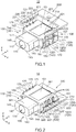
- a connector structure 10 according to a first embodiment of the present invention comprises a connector 100 and a board 200.
- the connector 100 is attached to the board 200 to form the connector structure 10.
- the connector 100 has an accommodation portion 110 which accommodates, at least in part, a mating connector (not shown) which is a plug.
- the accommodation portion 110 is a space which extends in a front-rear direction (Y-direction, first horizontal direction) perpendicular to an upper-lower direction (Z-direction).
- the accommodation portion 110 has a circular shape in a cross-section perpendicular to the front-rear direction.
- the connector 100 comprises a plurality of contacts 120 (or 1201 to 1206) and a housing (holding member) 130 which holds the contacts 120.
- Each of the contacts 120 is made of conductive metal plate, and the housing 130 is made of insulating resin.
- the number of the contacts 120 is six.
- the connector 100 according to the present embodiment comprises the first to sixth contacts 1201 to 1206.
- the present invention is not limited thereto.
- the number of the contacts 120 can be variously designed in accordance with the number of mating contact portions of mating contact.
- each of the contacts 120 (1201 to 1206) can be variously designed in accordance with various factors such as the shape of the mating contact and the shape of the housing 130. For example, a plurality of the contacts 120 may have shapes same as one another.
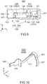
- each of the first contact 1201 to the sixth contact 1206, regardless of its shape, has a held portion 121, a first support portion (support portion) 123, a second support portion 125, a first contact portion (contact portion) 127 and a second contact portion (additional contact portion) 129.
- the held portion 121 is held by the housing 130.
- the first support portion 123 extends from the held portion 121 to be resiliently deformable.
- the first contact portion 127 is held by the first support portion 123 and is movable at least in a left-right direction (X-direction, second horizontal direction) because of the resilient deformation of the first support portion 123.
- the left-right direction is a direction perpendicular to both the upper-lower direction and the front-rear direction.
- the second support portion 125 extends from the held portion 121 to be resiliently deformable like the first support portion 123.
- the second contact portion 129 is held by the second support portion 125 and is movable at least in a predetermined direction perpendicular to the front-rear direction because of the resilient deformation of the second support portion 125.
- the predetermined direction of each of the first contact 1201 to the fifth contact 1205 is the left-right direction
- the predetermined direction of the sixth contact 1206 is a direction intersecting with both the upper-lower direction and the left-right direction.
- Each of the contacts 120 can be formed by punching out a metal plate and subsequently bending the metal plate.
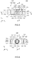
- the housing 130 has a front portion 140 and a rear portion 150 which continuously extend in the front-rear direction.
- the rear portion 150 has a rectangular parallelepiped shape.
- the rear portion 150 has an upper surface 151, a lower surface 153, a front surface 155, a rear surface 157 and a pair of side surfaces 161 and 163.
- the upper surface 151 and the lower surface 153 are apart from each other in the upper-lower direction.
- the front surface 155 and the rear surface 157 are apart from each other in the front-rear direction.
- the side surfaces 161 and 163 are apart from each other in the left-right direction.
- the front portion 140 projects forward, or in the negative Y-direction, from the front surface 155 of the rear portion 150.
- the front portion 140 has an upper surface 141, a lower surface 143, a pair of side surfaces 145 and a front surface 147.
- Each of the upper surface 141 and the lower surface 143 is a flat plane.
- Each of the side surfaces 145 is bent outward.
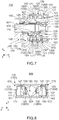
- the housing 130 has the accommodation portion 110.
- the accommodation portion 110 is formed within the housing 130 and opens at the front surface 147 of the front portion 140. As shown in Fig. 7 , the accommodation portion 110 extends to the vicinity of the rear surface 157 of the rear portion 150 in the front-rear direction.
- each of the side surfaces 161 and 163 of the housing 130 is formed with a plurality of side recesses 170.
- Each of the side recesses 170 is recessed inward in the left-right direction from one of the side surfaces 161 and 163 toward the inside of the housing 130.
- each of the side recesses 170 is a recess which has a rectangular shape when seen along the upper-lower direction.
- each of the side recesses 170 is surrounded on its three sides by two vertical walls (protection portions) 171 and one lateral wall (additional protection portion) 173.
- each of the side recesses 170 is formed by the two vertical walls 171 and the one lateral wall 173.
- Each of the two vertical walls 171 extends in the upper-lower direction.
- the two vertical walls 171 are apart from each other in the front-rear direction.
- the lateral wall 173 extends in the front-rear direction.
- the lateral wall 173 couples ends of the vertical walls 171 to each other.
- the side recesses 170 correspond to the contacts 120, respectively. Therefore, the side surface 161 is formed with three of the side recesses 170, and the other side surface 163 is formed with remaining three of the side recesses 170.
- the present invention is not limited thereto.
- the number and the arrangement of the side recesses 170 can be variously designed in accordance with the number and the arrangement of the contacts 120.
- the housing 130 has two holding portions 131 each of which holds the held portions 121 of three of the contacts 120.
- the holding portions 131 of the housing 130 hold the held portion 121 of each of the contacts 120.
- the first contact portions 127 of the thus-held contacts 120 are arranged in two rows each of which extends along the front-rear direction.
- the first contact portion 127 of each of the contacts 120 is positioned within the corresponding side recess 170 and faces outward in the left-right direction.
- the first support portion 123 which supports the first contact portion 127, is partially positioned within the corresponding side recess 170.
- Each of the second contact portions 129 projects in the accommodation portion 110.
- the second support portion 125, which supports the second contact portion 129, is partially positioned within the accommodation portion 110.
- the housing 130 may be formed integrally with the contacts 120 via integral molding.
- each of the first contact portions 127 is apart from the nearest vertical wall 171 by a distance which is shorter than the minimum one of distances each of which is a distance between the two first contact portions 127 adjacent to each other.
- the vertical wall 171 hides the first contact portion 127 and hides, at least in part, the first support portion 123 when seen along the front-rear direction.
- the lateral wall 173 hides the first contact portion 127 and the first support portion 123 when seen along the upper-lower direction.
- the first contact portion 127 of each of the contacts 120 is positioned within the corresponding side recess 170 and does not project outward beyond the side surface 161 or 163 in the left-right direction.
- each of the vertical walls 171 works as a protection portion that protects the corresponding first contact portion 127
- at least a part of each of the lateral walls 173 works as an additional protection portion that protects the corresponding first contact portion 127.
- the housing 130 has the protection portions and the additional protection portions each of which protects the corresponding first contact portion 127.
- each of the vertical walls 171 has two parts which are apart from each other in the upper-lower direction so that a gap is formed therebetween. According to the present embodiment, when each of the vertical walls 171 is seen along the front-rear direction, none of the first support portion 123 and the first contact portion 127 is visible through the gap between the two parts thereof.
- each of the first support portion 123 and the first contact portion 127 may be visible through the gap between the two parts of each of the vertical walls 171.
- the two parts of each of the vertical walls 171 may be formed into a single part with no gap.
- each of the vertical walls 171 is separated from the corresponding holding portion 131, which holds the corresponding contact 120, in the left-right direction.
- each of the vertical walls 171 may be continued to the corresponding holding portion 131.
- the board 200 has a principal surface 201 and a recess 210 which accommodates, at least in part, the connector 100.
- the recess 210 has a size which is so large as to accommodate a corresponding part of the housing 130 of the connector 100.
- the board 200 has a plurality of projecting portions 220. According to the present embodiment, each of the projecting portions 220 projects inward in the left-right direction within the recess 210. However, each of the projecting portions 220 may project in a direction which is perpendicular to the upper-lower direction and intersects with the first horizontal direction.
- the projecting portions 220 correspond to the side recesses 170 of the connector 100, respectively.
- Each of the projecting portions 220 has a rectangular shape when seen along the upper-lower direction and is smaller than the corresponding side recess 170 in the front-rear direction.
- Each of the projecting portions 220 has an end which is provided with a board-side contact portion 221.
- the board 200 has a plurality of the board-side contact portions 221 which are formed on the projecting portions 220, respectively.
- the board-side contact portions 221 correspond to the contacts 120 of the connector 100, respectively.
- each of the first contact portions 127 is brought into contact with the corresponding board-side contact portion 221 in the left-right direction.
- each of the first contact portions 127 may be brought into contact with the corresponding board-side contact portion 221 in a direction which is perpendicular to the upper-lower direction and intersects with the front-rear direction.
- the connector 100 is, at least in part, arranged within the recess 210 of the board 200 when attached to the board 200.
- the recess 210 of the board 200 partially accommodates the rear portion 150 of the connector 100.
- the recess 210 is recessed in a direction in parallel to the principal surface 201 of the board 200, or in the positive Y-direction, and opens in another direction in parallel to the principal surface 201 of the board 200, or in the negative Y-direction.
- the present invention is not limited thereto.
- the recess 210 may be closed in every direction in parallel to the principal surface 201 of the board 200.
- the recess 210 may be a hole which is formed at a position apart from the edge of the board 200 so as to pass through the board 200 in a direction perpendicular to the principal surface 201 of the board 200, or in the upper-lower direction. Moreover, when the board 200 has a sufficient thickness, the recess 210 may be an indention which is formed on the board 200 to have a bottom. Moreover, although the board 200 of the present embodiment is assumed to be rigid, the board 200 may have flexibility.
- the connector 100 when the connector 100 is attached to the board 200, the upper-lower direction with respect to the connector 100 intersects with, preferably perpendicular to, the principal surface 201 of the board 200.
- the connector 100 is first positioned under the board 200, or positioned toward the negative Z-side of the board 200, and subsequently moved upward, or moved in the positive Z-direction, so that the connector 100 is attached to the board 200.
- the first contact portions 127 and the first support portions 123 of the connector 100 are protected by the protection portions, or by the vertical walls 171.
- the vertical walls 171 are moved into the recess 210 of the board 200 at first, and subsequently the first contact portions 127 of the contacts 120 are brought into contact with the board-side contact portions 221, respectively.
- This process sequence prevents each of the contacts 120 from being buckled or damaged.
- the vertical walls 171 are, at least in part, positioned within the recess 210 of the board 200 to prevent or restrict the movement of the connector 100 relative to the board 200 in the front-rear direction. Therefore, each of the contacts 120 receives no substantial force in the front-rear direction from the board 200. As a result, each of the contacts 120 is prevented from being buckled or damaged.
- the lateral walls 173 prevent the connector 100 from being attached to the board 200 under an upside-down state.
- the lateral walls 173 prevent the ends of the contacts 120 from being brought into contact with the board-side contact portions 221. As a result, each of the contacts 120 is further prevented from being buckled or damaged.
- the mating connector (not shown) is a phone plug such as a terminal of a headphone and has the mating contact (not shown) of a cylindrical shape.
- the mating contact has a plurality of the mating contact portions (not shown) which are arranged in an axial direction and insulated from one another. Each of the mating contact portions is a part of a circumference surface of the mating contact.
- the second contact portions 129 of the contacts 120 are arranged at positions different from one another in the front-rear direction so as to correspond to the mating contact portions, respectively.
- each of the second contact portions 129 projects in the accommodation portion 110. When the mating contact is accommodated in the accommodation portion 110, each of the second contact portions 129 is brought into contact with the corresponding mating contact portion. As a result, each of the second contact portions 129 is electrically connected with the corresponding mating contact portion.
- a connector structure 10A according to a second embodiment of the present invention has a structure almost same as that of the connector structure 10 (see Figs. 1 to 7 ) according to the aforementioned first embodiment.
- components shown in Figs. 16 to 22 which are same as those of the first embodiment are referred by using reference signs same as those of the first embodiment.
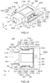
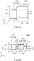
- the connector structure 10A according to the present embodiment is different from the connector structure 10 of the first embodiment in a shape of a housing (holding member) 130A of a connector 100A and in a shape of a board 200A. More specifically, as shown in Figs. 16 to 18 , 20 and 22 , the housing 130A has a rear portion 150A which has side surfaces 161A and 163A each of which is formed with one side recess 170A. Each of the side recesses 170A is a recess which has a rectangular shape when seen along the upper-lower direction.
- Each of the side recesses 170A is surrounded on its three sides by two vertical walls (protection portions) 171A, each of which extends in the upper-lower direction, and one lateral wall (additional protection portion) 173A extending in the front-rear direction.
- each of the side recesses 170A is formed by the two vertical walls 171A and the one lateral wall 173A of the housing 130A.
- Each of the side recesses 170A contains the first contact portions 127 of three of the contacts 120 positioned therein. Thus, three of the first contact portions 127 are positioned between the two vertical walls 171A of each of the side surfaces 161A and 163A.
- the board 200A has a recess 210A which accommodates, at least in part, the connector 100.
- the board 200A has a pair of projecting portions 220A each of which projects inward in the left-right direction within the recess 210A.
- the projecting portions 220A correspond to the side recesses 170A of the connector 100A, respectively.
- Each of the projecting portions 220A has a rectangular shape when seen along the upper-lower direction.
- Each of the projecting portions 220A has an end formed with a plurality of the board-side contact portions 221.
- the board-side contact portions 221 correspond to the contacts 120 of the connector 100A, respectively.
- the vertical wall 171A hides the first contact portions 127 like the first embodiment when seen along the front-rear direction. Moreover, the vertical wall 171A hides, at least in part, the first support portions 123. In addition, as can be seen from Fig. 19 , the lateral wall 173A hides the first contact portions 127 and the first support portions 123 when seen along the upper-lower direction. In other words, the first contact portion 127 of each of the contacts 120 is positioned within one of the side recesses 170A and does not project outward beyond the side surface 161A or 163A.
- each of the vertical walls 171A works as the protection portion that protects the corresponding first contact portions 127
- at least a part of each of the lateral walls 173A works as the additional protection portion that protects the corresponding first contact portions 127. Therefore, in the present embodiment, each of the contacts 120 is prevented from being buckled or damaged like the first embodiment.
- each of the lateral walls 173A is positioned opposite to the first support portions 123 across the first contact portions 127 and prevents the board 200A from being partially inserted into the side recess 170A.
- the board 200A can be inserted into the side recesses 170A only from a predetermined side of the connector 100A, wherein the predetermined side is provided with the first support portions 123 with no lateral wall 173A.
- the lateral walls 173A prevent the ends of the contacts 120 from being brought into contact with the board-side contact portions 221.
- each of the contacts 120 is prevented from being buckled or damaged.
- a gap is formed between the end of the contact 120 and the lateral wall 173A.
- the contact 120 may be designed so that the gap between the contact 120 and the lateral wall 173A remains even when the contact 120 is resiliently deformed. Instead, the contact 120 may be designed so as to be brought into abutment with the lateral wall 173A when the contact 120 is resiliently deformed.
- a connector structure 10B according to a third embodiment of the present invention has a structure almost same as that of the connector structure 10 (see Figs. 1 and 2 ) according to the aforementioned first embodiment.
- components shown in Figs. 23 and 24 which are same as those of the first embodiment are referred by using reference signs same as those of the first embodiment.
- the connector structure 10B comprises a connector 100B and a board 200B.
- the connector 100B has a plurality of contacts 120B and a housing (holding member) 130B which holds these contacts 120B.
- the contacts 120B have shapes different from one another.
- each of the contacts 120B has a held portion (not shown) held by the housing 130B, a first support portion (support portion) 123B extending from the held portion and a first contact portion (contact portion) 127B supported by the first support portion 123B.
- the first support portion 123B is resiliently deformable.
- the first contact portion 127B is movable at least in the upper-lower direction because of the resilient deformation of the first support portion 123B.
- first contact portions 127B of a plurality of the contacts 120B which are positioned at a side surface 161B, are seen along the left-right direction, they are positioned at positions same as one another in the upper-lower direction and arranged in the front-rear direction.
- the aforementioned arrangement is also applied to the first contact portions (not shown) positioned at another side surface 163B.
- the housing 130B has a rear portion 150B which has side recesses 170B each of which is formed at one of the side surfaces 161B and 163B.
- the housing 130B has vertical walls (protection portions) 171B which form the side recesses 170B.
- the first support portions 123B and the first contact portions 127B are positioned between two of the vertical walls 171B.
- the aforementioned arrangement is also applied to the other side surface 163B.
- the vertical wall 171B hides the first contact portions 127B and the first support portions 123B when seen along the front-rear direction.
- the board 200B has a recess 210B which accommodates, at least in part, the connector 100B.
- the board 200B has projecting portions 220B each of which projects inward in the left-right direction within the recess 210B.
- each of the projecting portions 220B has a lower surface which is formed with board-side contact portions (not shown).
- the board-side contact portions of the projecting portions 220B correspond to the first contact portions 127B of the contacts 120B, respectively.
- each of the first contact portions 127B of the connector 100B is brought into contact and electrically connected with the corresponding board-side contact portion.
- each of the first contact portion 127B is brought into contact with the corresponding board-side contact portion in the upper-lower direction.
- each of the vertical walls 171B works as the protection portion that protects the corresponding first contact portions 127B and the corresponding first support portions 123B. In the present embodiment, this protection prevents each of the contacts 120B from being buckled or damaged like the first embodiment and the second embodiment.
- the present invention has been described with specific embodiments, the present invention is not limited to the aforementioned embodiments but can be variously modified and changed.
- the contacts 120 120 (120, 120B) may be provided at only one of the side surfaces 161 and 163 (one of 161A and 163A, one of 161B and 163B).
- the minimum number of the protection portions may be two.
- the protection portions are arranged to be apart from each other in the front-rear direction, and the first contact portions 127 (127, 127B) of the contacts 120 (120, 120B) are arranged therebetween.
- the protection portion hides the first contact portions 127 (127, 127B) of the contacts 120 (120, 120B) when seen along the front-rear direction.
- the contacts 120 (120, 120B) may be provided at the rear surface 157 of the housing 130 (130A, 130B).
- the protection portions are arranged to be apart from one another in the left-right direction (first horizontal direction), and the first contact portions 127 (127, 127B) of the contacts 120 (120, 120B) are arranged therebetween.
- the protection portion hides the first contact portions 127 (127, 127B) of the contacts 120 (120, 120B) when seen along the left-right direction.
- the connector of each of the aforementioned embodiments has no fixing portion that fixes the connector to the board, the connector may be provided with a fixing portion that fixes the connector to the board.
Landscapes
- Coupling Device And Connection With Printed Circuit (AREA)
- Details Of Connecting Devices For Male And Female Coupling (AREA)
Description
- This invention relates to a connector and, in particular, relates to a connector partially accommodated in a recess of a board.
- For example, a connector partially accommodated in a recess of a board is disclosed in
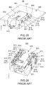
CN 204144492U (Patent Document 1). Referring toFig. 25 , Patent Document 1 discloses aconnector 900 which is attached to aboard 950 to form aconnector structure 90. - As can be seen from
Fig. 25 , theboard 950 has arecess 955 which partially accommodates the connector therewithin. Therecess 955 is recessed in a direction perpendicular to an upper-lower direction (Z-direction). Theboard 950 has an inner edge portion that defines therecess 955. The inner edge portion is provided with board-side contact portions 957. - As shown in
Figs. 25 and 26 , theconnector 900 comprises a plurality ofcontacts 910 and a housing (holding member) 930 which holds thecontacts 910. Each of thecontacts 910 has asupport portion 911, which is resiliently deformable, and acontact portion 913 held by thesupport portion 911. Thecontact portion 913 is exposed outward from aside surface 931 of thehousing 930. Thesupport portion 911 is, at least in part, accommodated in anindention 933 formed in thehousing 930. In particular, anend 915 of thesupport portion 911 is accommodated within theindention 933. - As can be seen from
Fig. 25 , theconnector 900 is moved into therecess 955 of theboard 950 along the upper-lower direction to be partially arranged in therecess 955. Under a state where theconnector 900 is attached to theboard 950, theconnector 900 partially projects upward, or in the positive Z-direction, from a principal surface (upper surface) 951 of theboard 950 and partially projects downward, or in the negative Z-direction, from another principal surface (lower surface) 953 of theboard 950. The board-side contact portions 957 correspond to thecontact portions 913 of theconnector 900, respectively. Under the state where theconnector 900 is attached to theboard 950, each of thecontact portions 913 of theconnector 900 is electrically connected to the corresponding board-side contact portion 957. - According to the
connector 900 of Patent Document 1, theend 915 of thesupport portion 911 of thecontact 910 is accommodated within theindention 933 of thehousing 930. This accommodation prevents theend 915 of thesupport portion 911 from being brought into abutment with theboard 950 upon the movement of theconnector 900 into therecess 955 of theboard 950. Moreover, even if thecontact portion 913 of thecontact 910 receives a force along a direction perpendicular to the upper-lower direction, the movement of thesupport portion 911 is restricted. Therefore, according to theconnector 900 of Patent Document 1, thecontact 910 is prevented from being buckled. However, according to the structure of theconnector 900 of Patent Document 1, theend 915 of thesupport portion 911 of thecontact 910 is required to be accommodated within theindention 933 of thehousing 930 while thecontact portion 913 of thecontact 910 is exposed outward from theside surface 931 of thehousing 930. This requirement limits the flexibility of design of thecontact 910. Furthermore,US 2008/0268703 A1 discloses a connector according to the preamble of claim 1, which is an audio jack embedded in an open mounting slot of a printed circuit board. - Furthermore, from
US 7,238,059 B1 , an audio jack connector including an insulating housing and a first set and a second set of conductive contacts is known. - It is therefore an object of the present invention to provide a connector having a structure which is different from that of Patent Document 1 but can prevent a contact from being buckled or damaged.
- The present invention provides a connector according to claim 1.
- Another aspect of the present invention provides a connector comprising a plurality of contacts and a holding member which holds the contacts. The contacts are arranged along a predetermined direction. Each of the contacts has a held portion held by the holding member, a support portion extending from the held portion to be resiliently deformable and a contact portion supported by the support portion. The holding member has at least one protection portion which protects the contact. The protection portion hides the contact portion when seen along the predetermined direction.
- Still another aspect of the present invention provides a connector structure comprising the connector and the board.
- When the connector according to an aspect of the present invention is seen along the first horizontal direction, the protection portion hides the contact portion of the contact. Thus, the protection portion protects the contact. This structure prevents or reduces an undesirable force which might be applied to the contact portion by the board when the connector is attached to the board, so that the contact can be prevented from being buckled or damaged.
- An appreciation of the objectives of the present invention and a more complete understanding of its structure may be had by studying the following description of the preferred embodiment and by referring to the accompanying drawings.
-
-
Fig. 1 is a perspective view showing a connector structure according to a first embodiment of the present invention, wherein a connector of the connector structure is not attached to a board of the connector structure. -
Fig. 2 is another perspective view showing the connector structure ofFig. 1 , wherein the connector is attached to the board. -
Fig. 3 is a plan view showing the connector structure ofFig. 2 . -
Fig. 4 is a bottom view showing the connector of the connector structure ofFig. 3 . -
Fig. 5 is a right side view showing the connector ofFig. 4 . -
Fig. 6 is a front view showing the connector ofFig. 4 . -
Fig. 7 is a cross-sectional view showing the connector ofFig. 5 , taken along line A-A. -
Fig. 8 is a cross-sectional view showing the connector ofFig. 5 , taken along line B-B. -
Fig. 9 is a cross-sectional view showing the connector ofFig. 6 , taken along line C-C. -
Fig. 10 is a perspective view showing a first contact of the connector ofFig. 7 . -
Fig. 11 is a perspective view showing a second contact of the connector ofFig. 7 . -
Fig. 12 is a perspective view showing a third contact of the connector ofFig. 7 . -
Fig. 13 is a perspective view showing a fourth contact of the connector ofFig. 7 . -
Fig. 14 is a perspective view showing a fifth contact of the connector ofFig. 7 . -
Fig. 15 is a perspective view showing a sixth contact of the connector ofFig. 7 . -
Fig. 16 is a perspective view showing a connector structure according to a second embodiment of the present invention, wherein a connector of the connector structure is not attached to a board of the connector structure. -
Fig. 17 is another perspective view showing the connector structure ofFig. 16 , wherein the connector is attached to the board. -
Fig. 18 is a plan view showing the connector structure ofFig. 17 . -
Fig. 19 is a bottom view showing the connector of the connector structure ofFig. 18 . -
Fig. 20 is a right side view showing the connector ofFig. 19 . -
Fig. 21 is a front view showing the connector ofFig. 19 . -
Fig. 22 is a cross-sectional view showing the connector ofFig. 20 , taken along line D-D. -
Fig. 23 is a perspective view showing a connector structure according to a third embodiment of the present invention, wherein a connector of the connector structure is not attached to a board of the connector structure. -
Fig. 24 is another perspective view showing the connector structure ofFig. 23 , wherein the connector is attached to the board. -
Fig. 25 is a perspective view showing a connector structure of Patent Document 1, wherein a connector of the connector structure is attached to a board of the connector structure. -
Fig. 26 is a bottom perspective view showing the connector of the connector structure ofFig. 25 . - While the invention is susceptible to various modifications and alternative forms, specific embodiments thereof are shown by way of example in the drawings and will herein be described in detail. It should be understood, however, that the drawings and detailed description thereto are not intended to limit the invention to the particular form disclosed, but on the contrary, the intention is to cover all modifications, equivalents and alternatives falling within the spirit and scope of the present invention as defined by the appended claims.
- Referring to
Figs. 1 to 3 , aconnector structure 10 according to a first embodiment of the present invention comprises aconnector 100 and aboard 200. In the present embodiment, theconnector 100 is attached to theboard 200 to form theconnector structure 10. - As shown in
Figs. 1, 2 and6 to 9 , theconnector 100 has anaccommodation portion 110 which accommodates, at least in part, a mating connector (not shown) which is a plug. Theaccommodation portion 110 is a space which extends in a front-rear direction (Y-direction, first horizontal direction) perpendicular to an upper-lower direction (Z-direction). Theaccommodation portion 110 has a circular shape in a cross-section perpendicular to the front-rear direction. - As shown in
Figs. 1 to 3 and5 to 9 , theconnector 100 comprises a plurality of contacts 120 (or 1201 to 1206) and a housing (holding member) 130 which holds thecontacts 120. Each of thecontacts 120 is made of conductive metal plate, and thehousing 130 is made of insulating resin. - As can be seen from
Figs. 1 to 3 and7 , in the present embodiment, the number of thecontacts 120 is six. Specifically, theconnector 100 according to the present embodiment comprises the first tosixth contacts 1201 to 1206. However, the present invention is not limited thereto. The number of thecontacts 120 can be variously designed in accordance with the number of mating contact portions of mating contact. - As can be seen from
Figs. 7 to 15 , thefirst contact 1201 to thesixth contact 1206 have shapes different from one another. However, the present invention is not limited thereto. The shape of each of the contacts 120 (1201 to 1206) can be variously designed in accordance with various factors such as the shape of the mating contact and the shape of thehousing 130. For example, a plurality of thecontacts 120 may have shapes same as one another. As shown inFigs. 10 to 15 , each of thefirst contact 1201 to thesixth contact 1206, regardless of its shape, has a heldportion 121, a first support portion (support portion) 123, asecond support portion 125, a first contact portion (contact portion) 127 and a second contact portion (additional contact portion) 129. The heldportion 121 is held by thehousing 130. Thefirst support portion 123 extends from the heldportion 121 to be resiliently deformable. Thefirst contact portion 127 is held by thefirst support portion 123 and is movable at least in a left-right direction (X-direction, second horizontal direction) because of the resilient deformation of thefirst support portion 123. In the present embodiment, the left-right direction is a direction perpendicular to both the upper-lower direction and the front-rear direction. Thesecond support portion 125 extends from the heldportion 121 to be resiliently deformable like thefirst support portion 123. Thesecond contact portion 129 is held by thesecond support portion 125 and is movable at least in a predetermined direction perpendicular to the front-rear direction because of the resilient deformation of thesecond support portion 125. In the present embodiment, the predetermined direction of each of thefirst contact 1201 to thefifth contact 1205 is the left-right direction, while the predetermined direction of thesixth contact 1206 is a direction intersecting with both the upper-lower direction and the left-right direction. Each of thecontacts 120 can be formed by punching out a metal plate and subsequently bending the metal plate. - As shown in
Figs. 1 to 7 and9 , thehousing 130 has afront portion 140 and arear portion 150 which continuously extend in the front-rear direction. Therear portion 150 has a rectangular parallelepiped shape. In detail, therear portion 150 has anupper surface 151, alower surface 153, afront surface 155, arear surface 157 and a pair of side surfaces 161 and 163. Theupper surface 151 and thelower surface 153 are apart from each other in the upper-lower direction. Thefront surface 155 and therear surface 157 are apart from each other in the front-rear direction. The side surfaces 161 and 163 are apart from each other in the left-right direction. Thefront portion 140 projects forward, or in the negative Y-direction, from thefront surface 155 of therear portion 150. Thefront portion 140 has anupper surface 141, alower surface 143, a pair of side surfaces 145 and afront surface 147. Each of theupper surface 141 and thelower surface 143 is a flat plane. Each of the side surfaces 145 is bent outward. Thehousing 130 has theaccommodation portion 110. In detail, theaccommodation portion 110 is formed within thehousing 130 and opens at thefront surface 147 of thefront portion 140. As shown inFig. 7 , theaccommodation portion 110 extends to the vicinity of therear surface 157 of therear portion 150 in the front-rear direction. - As shown in
Figs. 1 to 3 ,5 ,7 and 8 , each of the side surfaces 161 and 163 of thehousing 130 is formed with a plurality of side recesses 170. Each of the side recesses 170 is recessed inward in the left-right direction from one of the side surfaces 161 and 163 toward the inside of thehousing 130. As shown inFig. 3 , each of the side recesses 170 is a recess which has a rectangular shape when seen along the upper-lower direction. As shown inFigs. 1, 2 and5 , each of the side recesses 170 is surrounded on its three sides by two vertical walls (protection portions) 171 and one lateral wall (additional protection portion) 173. In other words, each of the side recesses 170 is formed by the twovertical walls 171 and the onelateral wall 173. Each of the twovertical walls 171 extends in the upper-lower direction. The twovertical walls 171 are apart from each other in the front-rear direction. Thelateral wall 173 extends in the front-rear direction. Thelateral wall 173 couples ends of thevertical walls 171 to each other. As can be seen fromFigs. 1 to 3 ,5 and7 , in the present embodiment, the side recesses 170 correspond to thecontacts 120, respectively. Therefore, theside surface 161 is formed with three of the side recesses 170, and theother side surface 163 is formed with remaining three of the side recesses 170. However, the present invention is not limited thereto. The number and the arrangement of the side recesses 170 can be variously designed in accordance with the number and the arrangement of thecontacts 120. - As can be seen from
Figs. 7 to 9 , thehousing 130 has two holdingportions 131 each of which holds the heldportions 121 of three of thecontacts 120. In other words, the holdingportions 131 of thehousing 130 hold the heldportion 121 of each of thecontacts 120. Thefirst contact portions 127 of the thus-heldcontacts 120 are arranged in two rows each of which extends along the front-rear direction. Thefirst contact portion 127 of each of thecontacts 120 is positioned within thecorresponding side recess 170 and faces outward in the left-right direction. Moreover, thefirst support portion 123, which supports thefirst contact portion 127, is partially positioned within thecorresponding side recess 170. Each of thesecond contact portions 129 projects in theaccommodation portion 110. Thesecond support portion 125, which supports thesecond contact portion 129, is partially positioned within theaccommodation portion 110. Thehousing 130 may be formed integrally with thecontacts 120 via integral molding. - As can be seen from
Fig. 5 , three of thecontacts 120 are positioned at theside surface 161, and thefirst contact portions 127 thereof are arranged in the front-rear direction (pitch direction). Remaining three of thecontacts 120 are positioned at theother side surface 163, and thefirst contact portions 127 thereof are arranged in the front-rear direction (pitch direction). In the present embodiment, each of thefirst contact portions 127 is apart from the nearestvertical wall 171 by a distance which is shorter than the minimum one of distances each of which is a distance between the twofirst contact portions 127 adjacent to each other. - As can be seen from
Figs. 6 to 8 , under a state where no load is applied to thecontact 120, thevertical wall 171 hides thefirst contact portion 127 and hides, at least in part, thefirst support portion 123 when seen along the front-rear direction. Moreover, as can be seen fromFig. 4 , thelateral wall 173 hides thefirst contact portion 127 and thefirst support portion 123 when seen along the upper-lower direction. In other words, thefirst contact portion 127 of each of thecontacts 120 is positioned within thecorresponding side recess 170 and does not project outward beyond theside surface vertical walls 171 works as a protection portion that protects the correspondingfirst contact portion 127, and at least a part of each of thelateral walls 173 works as an additional protection portion that protects the correspondingfirst contact portion 127. As described above, in the present embodiment, thehousing 130 has the protection portions and the additional protection portions each of which protects the correspondingfirst contact portion 127. Moreover, in the present embodiment, each of thevertical walls 171 has two parts which are apart from each other in the upper-lower direction so that a gap is formed therebetween. According to the present embodiment, when each of thevertical walls 171 is seen along the front-rear direction, none of thefirst support portion 123 and thefirst contact portion 127 is visible through the gap between the two parts thereof. However, a part of each of thefirst support portion 123 and thefirst contact portion 127 may be visible through the gap between the two parts of each of thevertical walls 171. Moreover, the two parts of each of thevertical walls 171 may be formed into a single part with no gap. As shown inFigs. 7 and 8 , each of thevertical walls 171 is separated from the corresponding holdingportion 131, which holds thecorresponding contact 120, in the left-right direction. However, each of thevertical walls 171 may be continued to the corresponding holdingportion 131. - As shown in
Figs. 1 to 3 , theboard 200 has aprincipal surface 201 and arecess 210 which accommodates, at least in part, theconnector 100. Therecess 210 has a size which is so large as to accommodate a corresponding part of thehousing 130 of theconnector 100. In addition, theboard 200 has a plurality of projectingportions 220. According to the present embodiment, each of the projectingportions 220 projects inward in the left-right direction within therecess 210. However, each of the projectingportions 220 may project in a direction which is perpendicular to the upper-lower direction and intersects with the first horizontal direction. The projectingportions 220 correspond to the side recesses 170 of theconnector 100, respectively. Each of the projectingportions 220 has a rectangular shape when seen along the upper-lower direction and is smaller than thecorresponding side recess 170 in the front-rear direction. Each of the projectingportions 220 has an end which is provided with a board-side contact portion 221. Thus, theboard 200 has a plurality of the board-side contact portions 221 which are formed on the projectingportions 220, respectively. The board-side contact portions 221 correspond to thecontacts 120 of theconnector 100, respectively. When theconnector 100 is attached to theboard 200, thefirst contact portions 127 of theconnector 100 are brought into contact and electrically connected with the board-side contact portions 221, respectively. In the present embodiment, each of thefirst contact portions 127 is brought into contact with the corresponding board-side contact portion 221 in the left-right direction. However, each of thefirst contact portions 127 may be brought into contact with the corresponding board-side contact portion 221 in a direction which is perpendicular to the upper-lower direction and intersects with the front-rear direction. - As can be seen from
Figs. 2 and3 , theconnector 100 is, at least in part, arranged within therecess 210 of theboard 200 when attached to theboard 200. According to the present embodiment, therecess 210 of theboard 200 partially accommodates therear portion 150 of theconnector 100. According to the present embodiment, therecess 210 is recessed in a direction in parallel to theprincipal surface 201 of theboard 200, or in the positive Y-direction, and opens in another direction in parallel to theprincipal surface 201 of theboard 200, or in the negative Y-direction. However, the present invention is not limited thereto. For example, therecess 210 may be closed in every direction in parallel to theprincipal surface 201 of theboard 200. More specifically, therecess 210 may be a hole which is formed at a position apart from the edge of theboard 200 so as to pass through theboard 200 in a direction perpendicular to theprincipal surface 201 of theboard 200, or in the upper-lower direction. Moreover, when theboard 200 has a sufficient thickness, therecess 210 may be an indention which is formed on theboard 200 to have a bottom. Moreover, although theboard 200 of the present embodiment is assumed to be rigid, theboard 200 may have flexibility. - As can be seen from
Figs. 1 and 2 , when theconnector 100 is attached to theboard 200, the upper-lower direction with respect to theconnector 100 intersects with, preferably perpendicular to, theprincipal surface 201 of theboard 200. In detail, theconnector 100 is first positioned under theboard 200, or positioned toward the negative Z-side of theboard 200, and subsequently moved upward, or moved in the positive Z-direction, so that theconnector 100 is attached to theboard 200. During this attachment process, thefirst contact portions 127 and thefirst support portions 123 of theconnector 100 are protected by the protection portions, or by thevertical walls 171. In detail, in the attachment process of theconnector 100 to theboard 200, thevertical walls 171 are moved into therecess 210 of theboard 200 at first, and subsequently thefirst contact portions 127 of thecontacts 120 are brought into contact with the board-side contact portions 221, respectively. This process sequence prevents each of thecontacts 120 from being buckled or damaged. Moreover, thevertical walls 171 are, at least in part, positioned within therecess 210 of theboard 200 to prevent or restrict the movement of theconnector 100 relative to theboard 200 in the front-rear direction. Therefore, each of thecontacts 120 receives no substantial force in the front-rear direction from theboard 200. As a result, each of thecontacts 120 is prevented from being buckled or damaged. In addition, thelateral walls 173 prevent theconnector 100 from being attached to theboard 200 under an upside-down state. Thus, thelateral walls 173 prevent the ends of thecontacts 120 from being brought into contact with the board-side contact portions 221. As a result, each of thecontacts 120 is further prevented from being buckled or damaged. - The mating connector (not shown) is a phone plug such as a terminal of a headphone and has the mating contact (not shown) of a cylindrical shape. The mating contact has a plurality of the mating contact portions (not shown) which are arranged in an axial direction and insulated from one another. Each of the mating contact portions is a part of a circumference surface of the mating contact. As can be seen from
Figs. 7 and9 , thesecond contact portions 129 of thecontacts 120 are arranged at positions different from one another in the front-rear direction so as to correspond to the mating contact portions, respectively. As can be seen fromFigs. 6 to 9 , each of thesecond contact portions 129 projects in theaccommodation portion 110. When the mating contact is accommodated in theaccommodation portion 110, each of thesecond contact portions 129 is brought into contact with the corresponding mating contact portion. As a result, each of thesecond contact portions 129 is electrically connected with the corresponding mating contact portion. - Referring to
Figs. 16 to 22 , aconnector structure 10A according to a second embodiment of the present invention has a structure almost same as that of the connector structure 10 (seeFigs. 1 to 7 ) according to the aforementioned first embodiment. Hereafter, components shown inFigs. 16 to 22 which are same as those of the first embodiment are referred by using reference signs same as those of the first embodiment. - As can be seen from comparison between
Figs. 16 to 22 andFigs. 1 to 7 , theconnector structure 10A according to the present embodiment is different from theconnector structure 10 of the first embodiment in a shape of a housing (holding member) 130A of aconnector 100A and in a shape of aboard 200A. More specifically, as shown inFigs. 16 to 18 ,20 and22 , thehousing 130A has arear portion 150A which hasside surfaces side recess 170A. Each of the side recesses 170A is a recess which has a rectangular shape when seen along the upper-lower direction. Each of the side recesses 170A is surrounded on its three sides by two vertical walls (protection portions) 171A, each of which extends in the upper-lower direction, and one lateral wall (additional protection portion) 173A extending in the front-rear direction. In other words, each of the side recesses 170A is formed by the twovertical walls 171A and the onelateral wall 173A of thehousing 130A. Each of the side recesses 170A contains thefirst contact portions 127 of three of thecontacts 120 positioned therein. Thus, three of thefirst contact portions 127 are positioned between the twovertical walls 171A of each of the side surfaces 161A and 163A. - As shown in
Figs. 16 to 18 , theboard 200A has arecess 210A which accommodates, at least in part, theconnector 100. In addition, theboard 200A has a pair of projectingportions 220A each of which projects inward in the left-right direction within therecess 210A. The projectingportions 220A correspond to the side recesses 170A of theconnector 100A, respectively. Each of the projectingportions 220A has a rectangular shape when seen along the upper-lower direction. Each of the projectingportions 220A has an end formed with a plurality of the board-side contact portions 221. The board-side contact portions 221 correspond to thecontacts 120 of theconnector 100A, respectively. - As can be seen from
Figs. 21 and 22 , in the present embodiment, thevertical wall 171A hides thefirst contact portions 127 like the first embodiment when seen along the front-rear direction. Moreover, thevertical wall 171A hides, at least in part, thefirst support portions 123. In addition, as can be seen fromFig. 19 , thelateral wall 173A hides thefirst contact portions 127 and thefirst support portions 123 when seen along the upper-lower direction. In other words, thefirst contact portion 127 of each of thecontacts 120 is positioned within one of the side recesses 170A and does not project outward beyond theside surface vertical walls 171A works as the protection portion that protects the correspondingfirst contact portions 127, and at least a part of each of thelateral walls 173A works as the additional protection portion that protects the correspondingfirst contact portions 127. Therefore, in the present embodiment, each of thecontacts 120 is prevented from being buckled or damaged like the first embodiment. Moreover, each of thelateral walls 173A is positioned opposite to thefirst support portions 123 across thefirst contact portions 127 and prevents theboard 200A from being partially inserted into theside recess 170A. Therefore, theboard 200A can be inserted into the side recesses 170A only from a predetermined side of theconnector 100A, wherein the predetermined side is provided with thefirst support portions 123 with nolateral wall 173A. Thus, thelateral walls 173A prevent the ends of thecontacts 120 from being brought into contact with the board-side contact portions 221. As a result, each of thecontacts 120 is prevented from being buckled or damaged. As shown inFig. 16 , according to the present embodiment, when thecontact 120 receives no load, a gap is formed between the end of thecontact 120 and thelateral wall 173A. Thecontact 120 may be designed so that the gap between thecontact 120 and thelateral wall 173A remains even when thecontact 120 is resiliently deformed. Instead, thecontact 120 may be designed so as to be brought into abutment with thelateral wall 173A when thecontact 120 is resiliently deformed. - Referring to
Figs. 23 and 24 , aconnector structure 10B according to a third embodiment of the present invention has a structure almost same as that of the connector structure 10 (seeFigs. 1 and 2 ) according to the aforementioned first embodiment. Hereafter, components shown inFigs. 23 and 24 which are same as those of the first embodiment are referred by using reference signs same as those of the first embodiment. - As shown in
Figs. 23 and 24 , theconnector structure 10B comprises aconnector 100B and aboard 200B. As shown inFig. 23 , theconnector 100B has a plurality ofcontacts 120B and a housing (holding member) 130B which holds thesecontacts 120B. Thecontacts 120B have shapes different from one another. However, each of thecontacts 120B has a held portion (not shown) held by thehousing 130B, a first support portion (support portion) 123B extending from the held portion and a first contact portion (contact portion) 127B supported by thefirst support portion 123B. Thefirst support portion 123B is resiliently deformable. Thefirst contact portion 127B is movable at least in the upper-lower direction because of the resilient deformation of thefirst support portion 123B. When thefirst contact portions 127B of a plurality of thecontacts 120B, which are positioned at aside surface 161B, are seen along the left-right direction, they are positioned at positions same as one another in the upper-lower direction and arranged in the front-rear direction. The aforementioned arrangement is also applied to the first contact portions (not shown) positioned at anotherside surface 163B. - As shown in
Figs. 23 and 24 , thehousing 130B has arear portion 150B which has side recesses 170B each of which is formed at one of the side surfaces 161B and 163B. Thehousing 130B has vertical walls (protection portions) 171B which form the side recesses 170B. At theside surface 161B, thefirst support portions 123B and thefirst contact portions 127B are positioned between two of thevertical walls 171B. The aforementioned arrangement is also applied to theother side surface 163B. Thevertical wall 171B hides thefirst contact portions 127B and thefirst support portions 123B when seen along the front-rear direction. - As shown in
Figs. 23 and 24 , theboard 200B has arecess 210B which accommodates, at least in part, theconnector 100B. Theboard 200B has projectingportions 220B each of which projects inward in the left-right direction within therecess 210B. As can be seen fromFigs. 23 and 24 , each of the projectingportions 220B has a lower surface which is formed with board-side contact portions (not shown). The board-side contact portions of the projectingportions 220B correspond to thefirst contact portions 127B of thecontacts 120B, respectively. When theconnector 100B is attached to theboard 200B, each of thefirst contact portions 127B of theconnector 100B is brought into contact and electrically connected with the corresponding board-side contact portion. In the present embodiment, each of thefirst contact portion 127B is brought into contact with the corresponding board-side contact portion in the upper-lower direction. - In the present embodiment, each of the
vertical walls 171B works as the protection portion that protects the correspondingfirst contact portions 127B and the correspondingfirst support portions 123B. In the present embodiment, this protection prevents each of thecontacts 120B from being buckled or damaged like the first embodiment and the second embodiment. - While the present invention has been described with specific embodiments, the present invention is not limited to the aforementioned embodiments but can be variously modified and changed. For example, although a plurality of the contacts 120 (120, 120B) are provided at each of the two
side surfaces 161 and 163 (161A and 163A, 161B and 163B) of the housing 130 (130A, 130B) according to the aforementioned embodiments, the contacts 120 (120, 120B) may be provided at only one of the side surfaces 161 and 163 (one of 161A and 163A, one of 161B and 163B). In this case, the minimum number of the protection portions (vertical walls rear surface 157 of the housing 130 (130A, 130B). In this case, the protection portions are arranged to be apart from one another in the left-right direction (first horizontal direction), and the first contact portions 127 (127, 127B) of the contacts 120 (120, 120B) are arranged therebetween. In this case, the protection portion hides the first contact portions 127 (127, 127B) of the contacts 120 (120, 120B) when seen along the left-right direction. Moreover, although the connector of each of the aforementioned embodiments has no fixing portion that fixes the connector to the board, the connector may be provided with a fixing portion that fixes the connector to the board.
Claims (10)
- A connector (100) attachable to a board (200) having a principal surface (201), a recess (210) and a board-side contact portion (221), wherein:the connector (100) is constructed in a way that, when the connector (100) is attached to the board (200), the connector (100) is, at least in part, arranged within the recess (210);the connector (100) comprises an accommodation portion (110) extending in a front-rear direction, also referred as first horizontal direction (Y) configured to be able to accommodate a mating connector; wherein an upper-lower direction (Z) is perpendicular to the first horizontal direction (Y);the connector (100) comprises at least one contact (120) and a holding member (130) which holds the contact (120);the contact (120) has a held portion (121) held by the holding member (130), a support portion (123) extending from the held portion (121) to be resiliently deformable and a contact portion (127) supported by the support portion (123);the connector (100) is constructed in a way that, when the connector (100) is attached to the board (200), the contact portion (127) is brought into contact with the board-side contact portion (221);the holding member (130) has at least one protection portion (171) which protects the contact (120);the connector (100) is constructed in a way that, when the connector (100) is attached to the board (200), the protection portion (171) is, at least in part, positioned within the recess (210); andthe holding member (130) has a side surface (161, 163) and a side recess (170) which is formed by walls and recessed inward from the side surface (161, 163);characterized in thatat least a part of the walls works as the protection portion (171);the support portion (123) and the contact portion (127) are positioned within the side recess (170); andthe connector (100) is constructed in a way that the protection portion (171) hides the support portion (123) and the contact portion (127) when seen along the first horizontal direction (Y).
- The connector (100) as recited in claim 1, wherein the at least one protection portion (171) includes two or more of the protection portions (171).
- The connector (100) as recited in claim 2, wherein the protection portions (171) are apart from one another in the first horizontal direction (Y).
- The connector (100) as recited in claim 3, wherein:
the at least one contact (120) includes a plurality of the contacts (120) which are positioned between the protection portions (171) in the first horizontal direction (Y). - The connector (100) as recited in one of claims 1 to 4, wherein:the holding member (130) has an additional protection portion (173); andthe additional protection portion (173) hides the contact portion (127) of the contact (120) when seen along the upper-lower direction (Z).
- The connector (100) as recited in one of claims 1 to 5, wherein the contact portion (127) is brought into contact with the board-side contact portion (221) in a direction (X) which is perpendicular to the upper-lower direction (Z) and intersects with the first horizontal direction (Y).
- The connector (100) as recited in one of claims 1 to 5, wherein the contact portion (127) is brought into contact with the board-side contact portion (221) in the upper-lower direction (Z).
- The connector (100) as recited in one of claims 1 to 7, wherein:the holding member (130) has the accommodation portion (110) which accommodates, at least in part, a mating connector having a mating contact portion;the contact (120) has an additional contact portion (129) which projects in the accommodation portion (110); andthe additional contact portion (129) is brought into contact with the mating contact portion when the mating connector is accommodated in the accommodation portion (110).
- A connector structure (10) comprising the connector (100) as recited in one of claims 1 to 8 and the board (200).
- The connector structure (10) as recited in claim 9, wherein:the board (200) has a projecting portion (220) projecting within the recess (210) in a direction which is perpendicular to the upper-lower direction (Z) and intersects with the first horizontal direction (Y); andthe board-side contact portion (221) is formed on the projecting portion (220).
Applications Claiming Priority (1)
| Application Number | Priority Date | Filing Date | Title |
|---|---|---|---|
| JP2016045551A JP6663754B2 (en) | 2016-03-09 | 2016-03-09 | connector |
Publications (2)
| Publication Number | Publication Date |
|---|---|
| EP3217486A1 EP3217486A1 (en) | 2017-09-13 |
| EP3217486B1 true EP3217486B1 (en) | 2019-01-09 |
Family
ID=58043923
Family Applications (1)
| Application Number | Title | Priority Date | Filing Date |
|---|---|---|---|
| EP17155891.9A Active EP3217486B1 (en) | 2016-03-09 | 2017-02-13 | Connector and connector structure |
Country Status (4)
| Country | Link |
|---|---|
| US (1) | US9899756B2 (en) |
| EP (1) | EP3217486B1 (en) |
| JP (1) | JP6663754B2 (en) |
| CN (1) | CN107181130B (en) |
Families Citing this family (2)
| Publication number | Priority date | Publication date | Assignee | Title |
|---|---|---|---|---|
| CN109390725A (en) * | 2017-08-02 | 2019-02-26 | 连展科技(深圳)有限公司 | All-in-One electric connector for socket |
| US10811798B2 (en) * | 2018-11-08 | 2020-10-20 | Te Connectivity Corporation | Card edge cable connector assembly |
Family Cites Families (22)
| Publication number | Priority date | Publication date | Assignee | Title |
|---|---|---|---|---|
| US3514737A (en) * | 1968-02-21 | 1970-05-26 | Amp Inc | Printed circuit board socket connector |
| JPS60147091U (en) * | 1984-03-07 | 1985-09-30 | ミツミティ−ア−ルダブリュ株式会社 | connector |
| JPH0541514Y2 (en) * | 1989-10-17 | 1993-10-20 | ||
| JP2558179Y2 (en) | 1992-10-12 | 1997-12-17 | ホシデン株式会社 | Jack type connector |
| JPH0922761A (en) | 1995-07-03 | 1997-01-21 | Nippondenso Co Ltd | Printed board installation/connection structure |
| JP2002117948A (en) | 2000-10-10 | 2002-04-19 | Sharp Corp | Optical plug |
| JP2003308933A (en) * | 2002-04-18 | 2003-10-31 | Hosiden Corp | Jack |
| CN2587091Y (en) * | 2002-11-23 | 2003-11-19 | 富士康(昆山)电脑接插件有限公司 | Electric coupler |
| US20060148314A1 (en) * | 2004-12-30 | 2006-07-06 | Motorola, Inc. | PCB mounted audio jack |
| TWM294771U (en) * | 2005-12-06 | 2006-07-21 | King Lion Entpr Co Ltd | Improvement of a headset connector structure |
| US7238059B1 (en) | 2006-06-06 | 2007-07-03 | Cheng Uei Precision Industry Co., Ltd. | Audio jack connector |
| TWM319560U (en) | 2007-04-27 | 2007-09-21 | Advanced Connectek Inc | Radio-frequency socket connector |
| CN201142390Y (en) * | 2007-12-06 | 2008-10-29 | 富士康(昆山)电脑接插件有限公司 | Electric connector |
| US20100055989A1 (en) * | 2008-09-03 | 2010-03-04 | Yu Hung Su | Audio jack connector |
| CN101800375B (en) * | 2009-02-07 | 2012-06-20 | 富士康(昆山)电脑接插件有限公司 | Socket connector and plug connector matched with same |
| CN201667469U (en) * | 2009-11-02 | 2010-12-08 | 富士康(昆山)电脑接插件有限公司 | Electric connector |
| EP2713448B1 (en) * | 2011-12-13 | 2016-03-23 | Huawei Device Co., Ltd. | Waterproof earphone jack |
| EP2793318A1 (en) * | 2012-05-16 | 2014-10-22 | Tyco Electronics Nederland B.V. | Electric connector |
| KR101499060B1 (en) | 2013-10-24 | 2015-03-06 | 주식회사 한빛티앤아이 | Waterproof Earphone Jack |
| CN103887643B (en) * | 2014-03-17 | 2016-04-13 | 小米科技有限责任公司 | Earphone socket, electronic device, electronic equipment and electronic system |
| CN203826667U (en) | 2014-03-17 | 2014-09-10 | 深圳君泽电子有限公司 | Waterproof earphone connector and mobile terminal with same |
| CN204144492U (en) | 2014-08-22 | 2015-02-04 | 富士康(昆山)电脑接插件有限公司 | Socket connector |
-
2016
- 2016-03-09 JP JP2016045551A patent/JP6663754B2/en active Active
-
2017
- 2017-01-06 US US15/399,934 patent/US9899756B2/en active Active
- 2017-02-06 CN CN201710066331.9A patent/CN107181130B/en active Active
- 2017-02-13 EP EP17155891.9A patent/EP3217486B1/en active Active
Non-Patent Citations (1)
| Title |
|---|
| None * |
Also Published As
| Publication number | Publication date |
|---|---|
| US9899756B2 (en) | 2018-02-20 |
| JP2017162648A (en) | 2017-09-14 |
| US20170264035A1 (en) | 2017-09-14 |
| JP6663754B2 (en) | 2020-03-13 |
| CN107181130A (en) | 2017-09-19 |
| CN107181130B (en) | 2020-04-17 |
| EP3217486A1 (en) | 2017-09-13 |
Similar Documents
| Publication | Publication Date | Title |
|---|---|---|
| JP5006618B2 (en) | connector | |
| JP5006610B2 (en) | connector | |
| US8177587B2 (en) | Connector with movable-side contact and fixed-side contact | |
| KR20150110313A (en) | Connector assembly | |
| US9252517B2 (en) | Connector | |
| JP7077177B2 (en) | connector | |
| EP3467948B1 (en) | Connector | |
| US10522929B2 (en) | Connector to provide reliable electrical connection | |
| US9979122B1 (en) | Electronic device and connector | |
| US9478902B2 (en) | Connector and connector unit | |
| TWI815170B (en) | Connector | |
| JP2020024851A (en) | Connector assembly | |
| EP3217486B1 (en) | Connector and connector structure | |
| JP2024052802A (en) | Movable connector and shield manufacturing method | |
| JP2008108560A (en) | Connector | |
| JP7044622B2 (en) | Connector assembly | |
| US7841879B2 (en) | Floating-type connector | |
| KR101307483B1 (en) | Connector | |
| EP3686911A1 (en) | Printed circuit board assembly | |
| JP2021093245A (en) | connector | |
| JP2022063421A (en) | connector | |
| JP2019185875A (en) | Connector device having terminal pressing structure | |
| JP7164947B2 (en) | movable connector | |
| JP2022063418A (en) | connector | |
| JP2014096286A (en) | Connector |
Legal Events
| Date | Code | Title | Description |
|---|---|---|---|
| PUAI | Public reference made under article 153(3) epc to a published international application that has entered the european phase |
Free format text: ORIGINAL CODE: 0009012 |
|
| STAA | Information on the status of an ep patent application or granted ep patent |
Free format text: STATUS: THE APPLICATION HAS BEEN PUBLISHED |
|
| AK | Designated contracting states |
Kind code of ref document: A1 Designated state(s): AL AT BE BG CH CY CZ DE DK EE ES FI FR GB GR HR HU IE IS IT LI LT LU LV MC MK MT NL NO PL PT RO RS SE SI SK SM TR |
|
| AX | Request for extension of the european patent |
Extension state: BA ME |
|
| STAA | Information on the status of an ep patent application or granted ep patent |
Free format text: STATUS: REQUEST FOR EXAMINATION WAS MADE |
|
| 17P | Request for examination filed |
Effective date: 20180201 |
|
| RBV | Designated contracting states (corrected) |
Designated state(s): AL AT BE BG CH CY CZ DE DK EE ES FI FR GB GR HR HU IE IS IT LI LT LU LV MC MK MT NL NO PL PT RO RS SE SI SK SM TR |
|
| STAA | Information on the status of an ep patent application or granted ep patent |
Free format text: STATUS: EXAMINATION IS IN PROGRESS |
|
| 17Q | First examination report despatched |
Effective date: 20180430 |
|
| GRAP | Despatch of communication of intention to grant a patent |
Free format text: ORIGINAL CODE: EPIDOSNIGR1 |
|
| STAA | Information on the status of an ep patent application or granted ep patent |
Free format text: STATUS: GRANT OF PATENT IS INTENDED |
|
| RIC1 | Information provided on ipc code assigned before grant |
Ipc: H01R 12/72 20110101ALI20180711BHEP Ipc: H01R 12/71 20110101ALN20180711BHEP Ipc: H01R 24/58 20110101AFI20180711BHEP |
|
| INTG | Intention to grant announced |
Effective date: 20180723 |
|
| GRAS | Grant fee paid |
Free format text: ORIGINAL CODE: EPIDOSNIGR3 |
|
| GRAA | (expected) grant |
Free format text: ORIGINAL CODE: 0009210 |
|
| STAA | Information on the status of an ep patent application or granted ep patent |
Free format text: STATUS: THE PATENT HAS BEEN GRANTED |
|
| AK | Designated contracting states |
Kind code of ref document: B1 Designated state(s): AL AT BE BG CH CY CZ DE DK EE ES FI FR GB GR HR HU IE IS IT LI LT LU LV MC MK MT NL NO PL PT RO RS SE SI SK SM TR |
|
| REG | Reference to a national code |
Ref country code: GB Ref legal event code: FG4D |
|
| REG | Reference to a national code |
Ref country code: CH Ref legal event code: EP Ref country code: AT Ref legal event code: REF Ref document number: 1088511 Country of ref document: AT Kind code of ref document: T Effective date: 20190115 |
|
| REG | Reference to a national code |
Ref country code: DE Ref legal event code: R096 Ref document number: 602017001736 Country of ref document: DE |
|
| REG | Reference to a national code |
Ref country code: IE Ref legal event code: FG4D |
|
| REG | Reference to a national code |
Ref country code: NL Ref legal event code: MP Effective date: 20190109 |
|
| REG | Reference to a national code |
Ref country code: LT Ref legal event code: MG4D |
|
| PG25 | Lapsed in a contracting state [announced via postgrant information from national office to epo] |
Ref country code: NL Free format text: LAPSE BECAUSE OF FAILURE TO SUBMIT A TRANSLATION OF THE DESCRIPTION OR TO PAY THE FEE WITHIN THE PRESCRIBED TIME-LIMIT Effective date: 20190109 |
|
| REG | Reference to a national code |
Ref country code: AT Ref legal event code: MK05 Ref document number: 1088511 Country of ref document: AT Kind code of ref document: T Effective date: 20190109 |
|
| PG25 | Lapsed in a contracting state [announced via postgrant information from national office to epo] |
Ref country code: ES Free format text: LAPSE BECAUSE OF FAILURE TO SUBMIT A TRANSLATION OF THE DESCRIPTION OR TO PAY THE FEE WITHIN THE PRESCRIBED TIME-LIMIT Effective date: 20190109 Ref country code: LT Free format text: LAPSE BECAUSE OF FAILURE TO SUBMIT A TRANSLATION OF THE DESCRIPTION OR TO PAY THE FEE WITHIN THE PRESCRIBED TIME-LIMIT Effective date: 20190109 Ref country code: PL Free format text: LAPSE BECAUSE OF FAILURE TO SUBMIT A TRANSLATION OF THE DESCRIPTION OR TO PAY THE FEE WITHIN THE PRESCRIBED TIME-LIMIT Effective date: 20190109 Ref country code: PT Free format text: LAPSE BECAUSE OF FAILURE TO SUBMIT A TRANSLATION OF THE DESCRIPTION OR TO PAY THE FEE WITHIN THE PRESCRIBED TIME-LIMIT Effective date: 20190509 Ref country code: NO Free format text: LAPSE BECAUSE OF FAILURE TO SUBMIT A TRANSLATION OF THE DESCRIPTION OR TO PAY THE FEE WITHIN THE PRESCRIBED TIME-LIMIT Effective date: 20190409 Ref country code: SE Free format text: LAPSE BECAUSE OF FAILURE TO SUBMIT A TRANSLATION OF THE DESCRIPTION OR TO PAY THE FEE WITHIN THE PRESCRIBED TIME-LIMIT Effective date: 20190109 |
|
| PG25 | Lapsed in a contracting state [announced via postgrant information from national office to epo] |
Ref country code: RS Free format text: LAPSE BECAUSE OF FAILURE TO SUBMIT A TRANSLATION OF THE DESCRIPTION OR TO PAY THE FEE WITHIN THE PRESCRIBED TIME-LIMIT Effective date: 20190109 Ref country code: HR Free format text: LAPSE BECAUSE OF FAILURE TO SUBMIT A TRANSLATION OF THE DESCRIPTION OR TO PAY THE FEE WITHIN THE PRESCRIBED TIME-LIMIT Effective date: 20190109 Ref country code: BG Free format text: LAPSE BECAUSE OF FAILURE TO SUBMIT A TRANSLATION OF THE DESCRIPTION OR TO PAY THE FEE WITHIN THE PRESCRIBED TIME-LIMIT Effective date: 20190409 Ref country code: LV Free format text: LAPSE BECAUSE OF FAILURE TO SUBMIT A TRANSLATION OF THE DESCRIPTION OR TO PAY THE FEE WITHIN THE PRESCRIBED TIME-LIMIT Effective date: 20190109 Ref country code: IS Free format text: LAPSE BECAUSE OF FAILURE TO SUBMIT A TRANSLATION OF THE DESCRIPTION OR TO PAY THE FEE WITHIN THE PRESCRIBED TIME-LIMIT Effective date: 20190509 Ref country code: GR Free format text: LAPSE BECAUSE OF FAILURE TO SUBMIT A TRANSLATION OF THE DESCRIPTION OR TO PAY THE FEE WITHIN THE PRESCRIBED TIME-LIMIT Effective date: 20190410 |
|
| REG | Reference to a national code |
Ref country code: DE Ref legal event code: R097 Ref document number: 602017001736 Country of ref document: DE |
|
| PG25 | Lapsed in a contracting state [announced via postgrant information from national office to epo] |
Ref country code: SK Free format text: LAPSE BECAUSE OF FAILURE TO SUBMIT A TRANSLATION OF THE DESCRIPTION OR TO PAY THE FEE WITHIN THE PRESCRIBED TIME-LIMIT Effective date: 20190109 Ref country code: RO Free format text: LAPSE BECAUSE OF FAILURE TO SUBMIT A TRANSLATION OF THE DESCRIPTION OR TO PAY THE FEE WITHIN THE PRESCRIBED TIME-LIMIT Effective date: 20190109 Ref country code: MC Free format text: LAPSE BECAUSE OF FAILURE TO SUBMIT A TRANSLATION OF THE DESCRIPTION OR TO PAY THE FEE WITHIN THE PRESCRIBED TIME-LIMIT Effective date: 20190109 Ref country code: LU Free format text: LAPSE BECAUSE OF NON-PAYMENT OF DUE FEES Effective date: 20190213 Ref country code: CZ Free format text: LAPSE BECAUSE OF FAILURE TO SUBMIT A TRANSLATION OF THE DESCRIPTION OR TO PAY THE FEE WITHIN THE PRESCRIBED TIME-LIMIT Effective date: 20190109 Ref country code: AL Free format text: LAPSE BECAUSE OF FAILURE TO SUBMIT A TRANSLATION OF THE DESCRIPTION OR TO PAY THE FEE WITHIN THE PRESCRIBED TIME-LIMIT Effective date: 20190109 Ref country code: AT Free format text: LAPSE BECAUSE OF FAILURE TO SUBMIT A TRANSLATION OF THE DESCRIPTION OR TO PAY THE FEE WITHIN THE PRESCRIBED TIME-LIMIT Effective date: 20190109 Ref country code: DK Free format text: LAPSE BECAUSE OF FAILURE TO SUBMIT A TRANSLATION OF THE DESCRIPTION OR TO PAY THE FEE WITHIN THE PRESCRIBED TIME-LIMIT Effective date: 20190109 Ref country code: EE Free format text: LAPSE BECAUSE OF FAILURE TO SUBMIT A TRANSLATION OF THE DESCRIPTION OR TO PAY THE FEE WITHIN THE PRESCRIBED TIME-LIMIT Effective date: 20190109 Ref country code: IT Free format text: LAPSE BECAUSE OF FAILURE TO SUBMIT A TRANSLATION OF THE DESCRIPTION OR TO PAY THE FEE WITHIN THE PRESCRIBED TIME-LIMIT Effective date: 20190109 |
|
| PLBE | No opposition filed within time limit |
Free format text: ORIGINAL CODE: 0009261 |
|
| STAA | Information on the status of an ep patent application or granted ep patent |
Free format text: STATUS: NO OPPOSITION FILED WITHIN TIME LIMIT |
|
| REG | Reference to a national code |
Ref country code: BE Ref legal event code: MM Effective date: 20190228 |
|
| REG | Reference to a national code |
Ref country code: IE Ref legal event code: MM4A |
|
| 26N | No opposition filed |
Effective date: 20191010 |
|
| PG25 | Lapsed in a contracting state [announced via postgrant information from national office to epo] |
Ref country code: IE Free format text: LAPSE BECAUSE OF NON-PAYMENT OF DUE FEES Effective date: 20190213 |
|
| PG25 | Lapsed in a contracting state [announced via postgrant information from national office to epo] |
Ref country code: SI Free format text: LAPSE BECAUSE OF FAILURE TO SUBMIT A TRANSLATION OF THE DESCRIPTION OR TO PAY THE FEE WITHIN THE PRESCRIBED TIME-LIMIT Effective date: 20190109 Ref country code: BE Free format text: LAPSE BECAUSE OF NON-PAYMENT OF DUE FEES Effective date: 20190228 |
|
| PG25 | Lapsed in a contracting state [announced via postgrant information from national office to epo] |
Ref country code: TR Free format text: LAPSE BECAUSE OF FAILURE TO SUBMIT A TRANSLATION OF THE DESCRIPTION OR TO PAY THE FEE WITHIN THE PRESCRIBED TIME-LIMIT Effective date: 20190109 |
|
| PG25 | Lapsed in a contracting state [announced via postgrant information from national office to epo] |
Ref country code: MT Free format text: LAPSE BECAUSE OF NON-PAYMENT OF DUE FEES Effective date: 20190213 |
|
| REG | Reference to a national code |
Ref country code: CH Ref legal event code: PL |
|
| PG25 | Lapsed in a contracting state [announced via postgrant information from national office to epo] |
Ref country code: LI Free format text: LAPSE BECAUSE OF NON-PAYMENT OF DUE FEES Effective date: 20200229 Ref country code: CH Free format text: LAPSE BECAUSE OF NON-PAYMENT OF DUE FEES Effective date: 20200229 |
|
| PG25 | Lapsed in a contracting state [announced via postgrant information from national office to epo] |
Ref country code: CY Free format text: LAPSE BECAUSE OF FAILURE TO SUBMIT A TRANSLATION OF THE DESCRIPTION OR TO PAY THE FEE WITHIN THE PRESCRIBED TIME-LIMIT Effective date: 20190109 |
|
| PG25 | Lapsed in a contracting state [announced via postgrant information from national office to epo] |
Ref country code: SM Free format text: LAPSE BECAUSE OF FAILURE TO SUBMIT A TRANSLATION OF THE DESCRIPTION OR TO PAY THE FEE WITHIN THE PRESCRIBED TIME-LIMIT Effective date: 20190109 |
|
| PG25 | Lapsed in a contracting state [announced via postgrant information from national office to epo] |
Ref country code: HU Free format text: LAPSE BECAUSE OF FAILURE TO SUBMIT A TRANSLATION OF THE DESCRIPTION OR TO PAY THE FEE WITHIN THE PRESCRIBED TIME-LIMIT; INVALID AB INITIO Effective date: 20170213 |
|
| PG25 | Lapsed in a contracting state [announced via postgrant information from national office to epo] |
Ref country code: MK Free format text: LAPSE BECAUSE OF FAILURE TO SUBMIT A TRANSLATION OF THE DESCRIPTION OR TO PAY THE FEE WITHIN THE PRESCRIBED TIME-LIMIT Effective date: 20190109 |
|
| PGFP | Annual fee paid to national office [announced via postgrant information from national office to epo] |
Ref country code: FR Payment date: 20230110 Year of fee payment: 7 |
|
| PGFP | Annual fee paid to national office [announced via postgrant information from national office to epo] |
Ref country code: FI Payment date: 20240213 Year of fee payment: 8 Ref country code: DE Payment date: 20231228 Year of fee payment: 8 Ref country code: GB Payment date: 20240108 Year of fee payment: 8 |