EP3188024B1 - Storage in a flash memory - Google Patents
Storage in a flash memory Download PDFInfo
- Publication number
- EP3188024B1 EP3188024B1 EP16161613.1A EP16161613A EP3188024B1 EP 3188024 B1 EP3188024 B1 EP 3188024B1 EP 16161613 A EP16161613 A EP 16161613A EP 3188024 B1 EP3188024 B1 EP 3188024B1
- Authority
- EP
- European Patent Office
- Prior art keywords
- page
- region
- data
- flash memory
- pcj
- Prior art date
- Legal status (The legal status is an assumption and is not a legal conclusion. Google has not performed a legal analysis and makes no representation as to the accuracy of the status listed.)
- Active
Links
- 230000015654 memory Effects 0.000 title claims description 57
- 238000012545 processing Methods 0.000 claims description 18
- 238000000034 method Methods 0.000 claims description 17
- 238000012790 confirmation Methods 0.000 claims description 4
- 238000013500 data storage Methods 0.000 claims description 2
- 238000007726 management method Methods 0.000 description 8
- 238000004891 communication Methods 0.000 description 6
- 230000008901 benefit Effects 0.000 description 4
- 238000010586 diagram Methods 0.000 description 4
- 238000012360 testing method Methods 0.000 description 4
- 238000012546 transfer Methods 0.000 description 3
- 239000000872 buffer Substances 0.000 description 2
- 238000012217 deletion Methods 0.000 description 2
- 230000037430 deletion Effects 0.000 description 2
- 230000008520 organization Effects 0.000 description 2
- 230000008569 process Effects 0.000 description 2
- 238000004458 analytical method Methods 0.000 description 1
- 238000013475 authorization Methods 0.000 description 1
- 238000006243 chemical reaction Methods 0.000 description 1
- 230000001627 detrimental effect Effects 0.000 description 1
- 238000005516 engineering process Methods 0.000 description 1
- 230000006870 function Effects 0.000 description 1
- 238000012986 modification Methods 0.000 description 1
- 230000004048 modification Effects 0.000 description 1
- 238000009877 rendering Methods 0.000 description 1
- 230000001131 transforming effect Effects 0.000 description 1
Images


Classifications
-
- G—PHYSICS
- G06—COMPUTING; CALCULATING OR COUNTING
- G06F—ELECTRIC DIGITAL DATA PROCESSING
- G06F3/00—Input arrangements for transferring data to be processed into a form capable of being handled by the computer; Output arrangements for transferring data from processing unit to output unit, e.g. interface arrangements
- G06F3/06—Digital input from, or digital output to, record carriers, e.g. RAID, emulated record carriers or networked record carriers
- G06F3/0601—Interfaces specially adapted for storage systems
- G06F3/0602—Interfaces specially adapted for storage systems specifically adapted to achieve a particular effect
- G06F3/062—Securing storage systems
- G06F3/0622—Securing storage systems in relation to access
-
- G—PHYSICS
- G06—COMPUTING; CALCULATING OR COUNTING
- G06F—ELECTRIC DIGITAL DATA PROCESSING
- G06F12/00—Accessing, addressing or allocating within memory systems or architectures
- G06F12/02—Addressing or allocation; Relocation
- G06F12/0223—User address space allocation, e.g. contiguous or non contiguous base addressing
- G06F12/023—Free address space management
- G06F12/0238—Memory management in non-volatile memory, e.g. resistive RAM or ferroelectric memory
- G06F12/0246—Memory management in non-volatile memory, e.g. resistive RAM or ferroelectric memory in block erasable memory, e.g. flash memory
-
- G—PHYSICS
- G06—COMPUTING; CALCULATING OR COUNTING
- G06F—ELECTRIC DIGITAL DATA PROCESSING
- G06F21/00—Security arrangements for protecting computers, components thereof, programs or data against unauthorised activity
-
- G—PHYSICS
- G06—COMPUTING; CALCULATING OR COUNTING
- G06F—ELECTRIC DIGITAL DATA PROCESSING
- G06F21/00—Security arrangements for protecting computers, components thereof, programs or data against unauthorised activity
- G06F21/70—Protecting specific internal or peripheral components, in which the protection of a component leads to protection of the entire computer
- G06F21/71—Protecting specific internal or peripheral components, in which the protection of a component leads to protection of the entire computer to assure secure computing or processing of information
- G06F21/72—Protecting specific internal or peripheral components, in which the protection of a component leads to protection of the entire computer to assure secure computing or processing of information in cryptographic circuits
-
- G—PHYSICS
- G06—COMPUTING; CALCULATING OR COUNTING
- G06F—ELECTRIC DIGITAL DATA PROCESSING
- G06F21/00—Security arrangements for protecting computers, components thereof, programs or data against unauthorised activity
- G06F21/70—Protecting specific internal or peripheral components, in which the protection of a component leads to protection of the entire computer
- G06F21/78—Protecting specific internal or peripheral components, in which the protection of a component leads to protection of the entire computer to assure secure storage of data
- G06F21/79—Protecting specific internal or peripheral components, in which the protection of a component leads to protection of the entire computer to assure secure storage of data in semiconductor storage media, e.g. directly-addressable memories
-
- G—PHYSICS
- G06—COMPUTING; CALCULATING OR COUNTING
- G06F—ELECTRIC DIGITAL DATA PROCESSING
- G06F3/00—Input arrangements for transferring data to be processed into a form capable of being handled by the computer; Output arrangements for transferring data from processing unit to output unit, e.g. interface arrangements
- G06F3/06—Digital input from, or digital output to, record carriers, e.g. RAID, emulated record carriers or networked record carriers
- G06F3/0601—Interfaces specially adapted for storage systems
- G06F3/0628—Interfaces specially adapted for storage systems making use of a particular technique
- G06F3/0629—Configuration or reconfiguration of storage systems
- G06F3/0631—Configuration or reconfiguration of storage systems by allocating resources to storage systems
-
- G—PHYSICS
- G06—COMPUTING; CALCULATING OR COUNTING
- G06F—ELECTRIC DIGITAL DATA PROCESSING
- G06F3/00—Input arrangements for transferring data to be processed into a form capable of being handled by the computer; Output arrangements for transferring data from processing unit to output unit, e.g. interface arrangements
- G06F3/06—Digital input from, or digital output to, record carriers, e.g. RAID, emulated record carriers or networked record carriers
- G06F3/0601—Interfaces specially adapted for storage systems
- G06F3/0628—Interfaces specially adapted for storage systems making use of a particular technique
- G06F3/0638—Organizing or formatting or addressing of data
- G06F3/064—Management of blocks
-
- G—PHYSICS
- G06—COMPUTING; CALCULATING OR COUNTING
- G06F—ELECTRIC DIGITAL DATA PROCESSING
- G06F3/00—Input arrangements for transferring data to be processed into a form capable of being handled by the computer; Output arrangements for transferring data from processing unit to output unit, e.g. interface arrangements
- G06F3/06—Digital input from, or digital output to, record carriers, e.g. RAID, emulated record carriers or networked record carriers
- G06F3/0601—Interfaces specially adapted for storage systems
- G06F3/0628—Interfaces specially adapted for storage systems making use of a particular technique
- G06F3/0655—Vertical data movement, i.e. input-output transfer; data movement between one or more hosts and one or more storage devices
- G06F3/0658—Controller construction arrangements
-
- G—PHYSICS
- G06—COMPUTING; CALCULATING OR COUNTING
- G06F—ELECTRIC DIGITAL DATA PROCESSING
- G06F3/00—Input arrangements for transferring data to be processed into a form capable of being handled by the computer; Output arrangements for transferring data from processing unit to output unit, e.g. interface arrangements
- G06F3/06—Digital input from, or digital output to, record carriers, e.g. RAID, emulated record carriers or networked record carriers
- G06F3/0601—Interfaces specially adapted for storage systems
- G06F3/0668—Interfaces specially adapted for storage systems adopting a particular infrastructure
- G06F3/0671—In-line storage system
- G06F3/0673—Single storage device
- G06F3/0679—Non-volatile semiconductor memory device, e.g. flash memory, one time programmable memory [OTP]
-
- G—PHYSICS
- G06—COMPUTING; CALCULATING OR COUNTING
- G06F—ELECTRIC DIGITAL DATA PROCESSING
- G06F9/00—Arrangements for program control, e.g. control units
- G06F9/06—Arrangements for program control, e.g. control units using stored programs, i.e. using an internal store of processing equipment to receive or retain programs
- G06F9/46—Multiprogramming arrangements
- G06F9/52—Program synchronisation; Mutual exclusion, e.g. by means of semaphores
- G06F9/526—Mutual exclusion algorithms
-
- G—PHYSICS
- G06—COMPUTING; CALCULATING OR COUNTING
- G06F—ELECTRIC DIGITAL DATA PROCESSING
- G06F2212/00—Indexing scheme relating to accessing, addressing or allocation within memory systems or architectures
- G06F2212/10—Providing a specific technical effect
- G06F2212/1052—Security improvement
-
- G—PHYSICS
- G06—COMPUTING; CALCULATING OR COUNTING
- G06F—ELECTRIC DIGITAL DATA PROCESSING
- G06F2212/00—Indexing scheme relating to accessing, addressing or allocation within memory systems or architectures
- G06F2212/72—Details relating to flash memory management
- G06F2212/7202—Allocation control and policies
-
- G—PHYSICS
- G06—COMPUTING; CALCULATING OR COUNTING
- G06F—ELECTRIC DIGITAL DATA PROCESSING
- G06F2212/00—Indexing scheme relating to accessing, addressing or allocation within memory systems or architectures
- G06F2212/72—Details relating to flash memory management
- G06F2212/7207—Details relating to flash memory management management of metadata or control data
Definitions
- the present description generally relates to electronic circuits and, more particularly, circuits using a flash memory.
- the present description aims more particularly at managing the storage of data in a flash memory.
- Flash memories are increasingly used in microcontrollers for nonvolatile storage of information.
- the storage of data in a flash memory presents various time constraints related to the granularity of the operations carried out, the writing and the reading being carried out by byte while the erasing is carried out by page.
- the atomicity of a transaction is to ensure that data stored in memory has a usable state. This is to ensure that data in non-volatile memory have either the state before the transaction or the state after the transaction concerned but they do not have an intermediate state.
- Transaction Atomicity Management is particularly used in applications where an interruption of circuit power or the occurrence of an accidental or deliberate disruption may result in the storage of data in a state rendering it unusable thereafter be vulnerable from the point of view of confidentiality.
- US2013117503A1 concerns data storage and more particularly the processing of storage requests for nonvolatile recording devices.
- FR2950463A1 relates to a method of reading a non-volatile memory by means of metadata and a correspondence table.
- the pages of the second region are used sequentially.
- each request to access a page of the memory begins by reading the metadata field of the corresponding page in the first region to determine whether the data is contained in this page or in a page of the second region.
- this page contains either the initial data or the final data, the intermediate data being contained in a page of the second region.
- One embodiment provides a method for managing a non-volatile memory in which data are stored by applying the above method.
- One embodiment provides a flash memory, programmed according to the above method.
- One embodiment provides an electronic circuit comprising a flash memory.
- the figure 1 represents very schematically and in block form, an embodiment of an electronic circuit 1 of the type to which, by way of example, apply the embodiments that will be described.
- the circuit 1 also includes a contactless communication circuit (CLF - ContactLess Front-end), of Near Field Communication (NFC) type.
- CLF contactless communication circuit
- NFC Near Field Communication
- circuit 1 can integrate other functions, symbolized by a block 17 (FCT), depending on the application, for example, a crypto-processor, other interfaces, other memories, etc.
- FCT a block 17
- a flash memory is programmed from an initial state to states 0 (non-conductive states of the cells). This means that the cells of the memory must be initialized to a high state and that, to store data, one chooses either not to intervene on the state of the bit, or to program this bit to 0.
- An erasure (reset in the initial state up) is necessarily made by memory page.
- a page is defined as the minimum size that can be addressed simultaneously for deletion. Typically, a page currently represents, in a flash memory, 32, 64, 128, 256 or 512 bytes. In practice, this corresponds to the size of a register receiving the data in series to transfer them in parallel to the memory plane for storage.
- the atomicity management methods activate a data processing indicator when it is extracted from the non-volatile memory, then organize the storage of the updated data, once the processing is completed, the processing indicator then changing state. Atomicity can concern a larger or smaller amount of data (bytes) depending on the nature of the transaction.
- the atomic character of the transactions is particularly important in the case of bank-type transactions (payment for example) where it is necessary to ensure that the information stored in the flash memory, for example the balance of an electronic purse or an authorization to purchase, or the identifier validating a transaction, is stored reliably.
- atomicity temporary storage spaces (Buffer) are used which are updated with the initial information, and then final, for transfer to the main non-volatile memory.
- Buffer atomicity temporary storage spaces
- the memory is a flash memory
- the need for erasure of the data is problematic because of its granularity per page, which makes the operation relatively long compared to the write operation which is bytes.
- the figure 2 is a block diagram illustrating the division of the flash memory 2 of the figure 1 in three regions.
- a first region 22 of the memory 2 is assigned to the storage of any information not contained in the other two zones that have particular roles.
- the stable information in data processing implementing an atomicity management are, between two transactions, stored in this main memory.
- a second region 24 is a so-called cache area (CA - Cache Area), intended to store information during their processing for the implementation of an atomicity process.
- CA - Cache Area a cache area
- a third region 26 is a so-called temporary information storage area (TIA) intended to store information indicative of the progress of a transaction using the first two regions and, in particular, flags representative of the state. data stored in other regions.
- TIA temporary information storage area
- Each page of the regions 22 and 24 includes a part dedicated to storing the data and a part dedicated to storing metadata giving information on the stability of the data and the possibility of storing the corresponding data in the other region 24 or 22.
- L use of pages in regions 22 and 24 is transparent to the user.
- the storage system can be seen as a memory region of N pages, the location of each page being either in the main region 22 or in the cache region 24.
- the figure 3 illustrates an exemplary page content of the regions 22 and 24 and the temporary region 26. It is assumed that the main region 22 contains n pages and that the cache region 24 contains m pages. Preferably, the number m of pages of the cache region is less than or equal to n. This number determines the number of atomic update operations that can be done before clearing the cache region, thus performing a relatively long operation.
- Each page P0, P1,..., Pi,..., Pn of the region 22 and PC0,..., PCj,..., PCm of the region 24 comprises data on a certain number of bytes (for example B0 to B6) and a metadata field (for example B7).
- the cache region 24 is empty, i.e. the pages have been erased and all the bits contain a state 1 (FF).
- the memory 2 is, in the usual way, equipped with a controller transforming logical addresses into physical addresses.
- a logical index page i one accesses the B7MD metadata field of the physical index page Pi i (or a conversion of this index) in the main region 22.
- This metadata indicate whether the data of the page in the main memory is correct (in practice, if the field is empty, it means that the data is correct). If it is not, the metadata box contains the physical index (address) PCj of the cache page in which the logical page containing the data is stored.
- the B7MD metadata area of the region 22 contains a field containing the address PCj in the region 24 that is programmed when a page of the region 22 is processed in the region 24.
- the B7MD metadata area of a page of the region 24 which contains data of the region 22 contains a field B7MD with the index or address Pi of the region 22 from which the data is extracted and a field containing an indicator flag of the use of the page, that is, programmed when the page is moved to the main region 22.
- the cache region 24 is sequentially filled from the first PC0 to the last PCM page as the data processing requirements in the region 2 become. Thus, as long as the region 24 is not full, the region 24 may continue to be used without the need for deletion.
- the temporary region 26 serves to protect the data content of the other two regions in the event of a transaction being interrupted.
- This region contains temporary information consisting of four indicators or flags F0, F1, F2, F3. These flags indicate, respectively, the beginning of an operation (F0), the nature of the operation (F1), a confirmation (F2) that the F1 flag is stable and the end of the operation (F3).
- the temporary information actually contains all that is necessary to reconstruct the data in case of interruption of the operation.
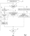
- the figure 4 is a block diagram illustrating the realization of an atomic data processing (block 30, ATOMIC PROCESS) on data contained in a page Pi of the region 22.
- steps 33 to 35 are performed if test 32 is executed after operation 33).
- At least one PCj page of the region 24 is deleted (block 36) in order to reuse it.
- block 36 we begin by erasing (block 36, ERASE P (B7MD (PCj))) a page P of the main region whose updated content is stored in region 22 by identifying the corresponding page Pi through the field B7MD of the PC page which contains the address of the corresponding page Pi. Then, the content of this page PCj in the main region 22 in the page Pi just deleted is transferred (block 36, PCj -> P (B7MD (PCj)) Finally, one erases (block 36, ERASE PCj ) the page PCj of the region 24 which can then be used again.
- step 34 (case shown) or step 34.
- step 35 is executed, it is tested whether the atomic operation is complete (block 37, AP END?). If yes (output Y of block 37), the processing stops (END). If not, return to step 31.
- step 36 all the PCj pages of the region 24 are deleted (block 36) in order to reuse them.
- block 36 ERASE P (B7MD (PCj))
- all the pages P of the main region whose updated content is stored in region 22 by identifying the corresponding pages Pi using the fields B7MD PCj pages which contain the addresses of the corresponding pages Pi.
- the contents of all these pages PCj in the main region 22 are transferred (block 36, PCj -> P (B7MD (PCj)) to the pages Pi which have just been erased
- one erases (block 36, ERASE PCj) all PCj pages of region 24.
- the cache region is then empty to be used sequentially again.
- the field B7MD (Pi) is not empty (output N of block 31) and indicates the address of a page PCj in region 24, it means that the data B0 to B6 of the page Pi are not valid (or are not stable data).
- the operation is then performed on the content of the PCj page (block 38, OPERATION ON PC (B7MD (Pi)) identified by the field B7MD of the page Pi.
- the result of the operation must be stored in a file. page Pi.
- the flag F0 is activated when starting the operation on the data, that is to say at the start of step 33 or 38, the flags F1 and F2 are also written at the start of step 33 or 38 to indicate the nature of the operation, and the flag F3 is activated before the test 37 to indicate the end of the operation.
- the described embodiment takes advantage of the difference in duration between the programming time and the erasure time.
- the operation of erasing a page is relatively long (typically of the order of a few milliseconds) compared to an operation programming a byte (typically of the order of ten microseconds).
- page size depends on the application and the maximum size needed to store a transaction.
- An advantage of the embodiments that have been described is that they improve the management of a flash memory for the processing of operations that must comply with an atomicity criterion.
Landscapes
- Engineering & Computer Science (AREA)
- Theoretical Computer Science (AREA)
- Physics & Mathematics (AREA)
- General Engineering & Computer Science (AREA)
- General Physics & Mathematics (AREA)
- Software Systems (AREA)
- Computer Hardware Design (AREA)
- Human Computer Interaction (AREA)
- Computer Security & Cryptography (AREA)
- Mathematical Physics (AREA)
- Techniques For Improving Reliability Of Storages (AREA)
- Information Retrieval, Db Structures And Fs Structures Therefor (AREA)
Description
La présente description concerne de façon générale les circuits électroniques et, plus particulièrement, les circuits exploitant une mémoire flash. La présente description vise plus particulièrement la gestion du stockage de données dans une mémoire flash.The present description generally relates to electronic circuits and, more particularly, circuits using a flash memory. The present description aims more particularly at managing the storage of data in a flash memory.
Les mémoires flash sont de plus en plus utilisées dans des microcontrôleurs pour stocker de façon non volatile des informations.Flash memories are increasingly used in microcontrollers for nonvolatile storage of information.
Le stockage de données dans une mémoire flash présente diverses contraintes temporelles liées à la granularité des opérations réalisées, l'écriture et la lecture s'effectuant par octet tandis que l'effacement s'effectue par page.The storage of data in a flash memory presents various time constraints related to the granularity of the operations carried out, the writing and the reading being carried out by byte while the erasing is carried out by page.
Dans certaines applications, on souhaite s'assurer que les transactions réalisées et stockées respectent un critère d'atomicité. L'atomicité d'une transaction correspond à s'assurer que des données stockées en mémoire présentent bien un état exploitable. Cela revient à s'assurer que des données en mémoire non volatile présentent soit l'état avant la transaction soit l'état après la transaction concernée mais qu'elles ne présentent pas un état intermédiaire.In certain applications, it is desired to ensure that the transactions carried out and stored comply with an atomicity criterion. The atomicity of a transaction is to ensure that data stored in memory has a usable state. This is to ensure that data in non-volatile memory have either the state before the transaction or the state after the transaction concerned but they do not have an intermediate state.
La gestion de l'atomicité de transaction est particulièrement utilisée dans des applications où une interruption de l'alimentation du circuit ou l'apparition d'une perturbation accidentelle ou volontaire peut engendrer le stockage de données dans un état les rendant soit inexploitables par la suite soit vulnérables du point de vue de la confidentialité.Transaction Atomicity Management is particularly used in applications where an interruption of circuit power or the occurrence of an accidental or deliberate disruption may result in the storage of data in a state rendering it unusable thereafter be vulnerable from the point of view of confidentiality.
On connait de nombreuses techniques de gestion d'atomicité, plus particulièrement dans des microcontrôleurs appliqués à des transactions dites de sécurité, par exemple des transactions bancaires, de contrôle d'accès, etc.Many atomic management techniques are known, more particularly in microcontrollers applied to so-called security transactions, for example banking transactions, access control, etc.
Il serait souhaitable de disposer d'une solution de stockage de données dans une mémoire flash qui respecte le critère d'atomicité des données manipulées.It would be desirable to have a solution for storing data in a flash memory that respects the atomicity criterion of the data manipulated.
Il serait souhaitable de disposer d'une solution particulièrement adaptée à des transactions basées sur des communications sans contact.It would be desirable to have a solution particularly suited to transactions based on contactless communications.
Ainsi, un mode de réalisation prévoit un procédé de stockage de données dans une mémoire non volatile, dans lequel la mémoire non volatile est divisée en :
- une première région dont chaque page comporte des champs destinés à contenir des données et un champ destiné à contenir des métadonnées ;
- une deuxième région dont chaque page comporte des champs destinés à contenir des données et un champ destiné à contenir des métadonnées ;
- une troisième région destinée à contenir des indicateurs du déroulement d'une opération dans les première et deuxième régions,
- les champs de métadonnées des première et deuxième régions étant respectivement destinés à contenir, lors d'une opération de mise à jour de données dans une page de la première région, les index d'une page dans la deuxième région et de ladite page de la première région.
- a first region where each page has fields for holding data and a field for holding metadata;
- a second region where each page has fields for holding data and a field for holding metadata;
- a third region intended to contain indicators of the progress of an operation in the first and second regions,
- the metadata fields of the first and second regions being respectively intended to contain, during a data update operation in a page of the first region, the indexes of a page in the second region and of said page of the first region.
Selon un mode de réalisation, les indicateurs sont au nombre de quatre et indiquent respectivement :
- le début d'une opération ;
- la nature de l'opération ;
- une confirmation que l'indicateur de nature de l'opération est stable ; et
- la fin de l'opération.
- the beginning of an operation;
- the nature of the operation;
- a confirmation that the nature indicator of the operation is stable; and
- the end of the operation.
Selon un mode de réalisation, les pages de la deuxième région sont utilisées séquentiellement.According to one embodiment, the pages of the second region are used sequentially.
Selon un mode de réalisation, à chaque demande d'accès à une page de la mémoire, on commence par lire le champ de métadonnées de la page correspondante dans la première région pour déterminer si les données sont contenues dans cette page ou dans une page de la deuxième région.According to one embodiment, each request to access a page of the memory begins by reading the metadata field of the corresponding page in the first region to determine whether the data is contained in this page or in a page of the second region.
Selon un mode de réalisation, lors d'un traitement atomique sur des données contenues dans une page de la première région, cette page contient soit les données initiales, soit les données finales, les données intermédiaires étant contenues dans une page de la deuxième région.According to one embodiment, during an atomic processing on data contained in a page of the first region, this page contains either the initial data or the final data, the intermediate data being contained in a page of the second region.
Un mode de réalisation prévoit un procédé de gestion d'une mémoire non volatile dans laquelle sont stockées des données par application du procédé ci-dessus.One embodiment provides a method for managing a non-volatile memory in which data are stored by applying the above method.
Un mode de réalisation prévoit une mémoire flash, programmée conformément au procédé ci-dessus.One embodiment provides a flash memory, programmed according to the above method.
Un mode de réalisation prévoit un circuit électronique comportant une mémoire flash.One embodiment provides an electronic circuit comprising a flash memory.
Ces caractéristiques et avantages, ainsi que d'autres, seront exposés en détail dans la description suivante de modes de réalisation particuliers faite à titre non limitatif en relation avec les figures jointes parmi lesquelles :
- la
figure 1 est un schéma-bloc d'un exemple de circuit électronique du type auquel s'appliquent les modes de réalisation qui vont être décrits ; - la
figure 2 est un schéma-bloc illustrant un mode d'organisation d'une mémoire flash ; - la
figure 3 illustre un mode de réalisation d'une affectation de données dans la mémoire de lafigure 2 ; et - la
figure 4 illustre, de façon très schématique et sous forme de blocs, un mode de mise en oeuvre d'un procédé de gestion du stockage dans la mémoire flash de lafigure 2 .
- the
figure 1 is a block diagram of an exemplary electronic circuit of the type to which the embodiments to be described apply; - the
figure 2 is a block diagram illustrating a mode of organization of a flash memory; - the
figure 3 illustrates an embodiment of a data assignment in the memory of thefigure 2 ; and - the
figure 4 illustrates very schematically and in the form of blocks, an embodiment of a storage management method in the flash memory of thefigure 2 .
De mêmes éléments ont été désignés par de mêmes références aux différentes figures.The same elements have been designated with the same references in the various figures.
Par souci de clarté, seuls les étapes et éléments utiles à la compréhension des modes de réalisation qui vont être décrits ont été représentés et seront détaillés. En particulier, le fonctionnement électrique d'une mémoire flash lors des étapes d'écriture, de lecture et d'effacement n'a pas été détaillé, les modes de réalisation décrits étant compatibles avec les technologies usuelles des mémoires flash. De plus, les applications utilisant une gestion d'atomicité n'ont pas non plus été détaillées, les modes de réalisation décrits étant, là encore, compatibles avec les applications usuelles.For the sake of clarity, only the steps and elements useful for understanding the embodiments that will be described have been shown and will be detailed. In particular, the electrical operation of a flash memory during the steps of writing, reading and erasing has not been detailed, the embodiments described being compatible with the usual technologies of flash memories. In addition, the applications using atomicity management have also not been detailed, the embodiments described being, again, compatible with the usual applications.
Dans la description qui suit, lorsqu'on fait référence aux termes approximativement, environ et, de l'ordre de, cela signifie à 10% près, de préférence à 5% près.In the following description, when referring to the terms approximately, approximately and, in the order of, this means to within 10%, preferably to within 5%.
La
Le circuit 1 comporte :
- une unité de traitement 11 (CORE), par exemple une machine d'états, un microprocesseur, un circuit logique programmable, etc. ;
- une ou plusieurs zones 12 (RAM) de stockage volatile, par exemple de type mémoire RAM ou registres, pour stocker temporairement des informations (instructions, adresses, données) pendant les traitements ;
- une ou plusieurs zones de stockage non volatile, dont au moins une
mémoire 2 de type flash (FLASH) pour stocker des informations de façon durable et en particulier quand le circuit n'est pas alimenté ; - un ou plusieurs
bus 14 de données, d'adresses et/ou de commande entre les différents éléments internes au circuit 1 ; et - une interface d'entrée-sortie 15 (I/O) de communication, par exemple de type bus série, avec l'extérieur du circuit 1.
- a processing unit 11 (CORE), for example a state machine, a microprocessor, a programmable logic circuit, etc. ;
- one or more volatile storage areas 12 (RAM), for example of RAM memory type or registers, for temporarily storing information (instructions, addresses, data) during the processing operations;
- one or more non-volatile storage areas, including at least one flash memory (FLASH) 2 for storing information in a durable manner and in particular when the circuit is not powered;
- one or
more buses 14 of data, addresses and / or control between the various elements internal to the circuit 1; and - an input / output interface 15 (I / O) for communication, for example of the serial bus type, with the outside of the circuit 1.
Dans les applications plus particulièrement visées par la présente description, le circuit 1 intègre également un circuit 16 de communication sans contact (CLF - ContactLess Front-end), de type communication en champ proche (Near Field Communication - NFC).In the applications more particularly targeted by the present description, the circuit 1 also includes a contactless communication circuit (CLF - ContactLess Front-end), of Near Field Communication (NFC) type.
Par ailleurs, le circuit 1 peut intégrer d'autres fonctions, symbolisées par un bloc 17 (FCT), selon l'application, par exemple, un crypto-processeur, d'autres interfaces, d'autres mémoires, etc.Furthermore, the circuit 1 can integrate other functions, symbolized by a block 17 (FCT), depending on the application, for example, a crypto-processor, other interfaces, other memories, etc.
La gestion de l'atomicité des transactions dans un circuit équipé d'une mémoire flash est particulière car la mémoire flash présente une granularité de traitement par page et non par bit ou par octet, en particulier pour l'effacement. Une mémoire flash se programme, à partir d'un état initial vers des états 0 (états non conducteurs des cellules) . Cela signifie que les cellules de la mémoire doivent être initialisées à un état haut et que, pour stocker une donnée, on choisit soit de ne pas intervenir sur l'état du bit, soit de programmer ce bit à 0. Un effacement (remise dans l'état initial haut) s'effectue forcément par page mémoire. Une page est définie comme la taille minimale susceptible d'être adressée simultanément pour effacement. Typiquement, une page représente actuellement, dans une mémoire flash, 32, 64, 128, 256 ou 512 octets. En pratique, cela correspond à la taille d'un registre recevant les données en série pour les transférer en parallèle au plan mémoire pour stockage.The management of the atomicity of transactions in a circuit equipped with a flash memory is particular because the flash memory has a processing granularity per page and not per bit or byte, especially for erasure. A flash memory is programmed from an initial state to states 0 (non-conductive states of the cells). This means that the cells of the memory must be initialized to a high state and that, to store data, one chooses either not to intervene on the state of the bit, or to program this bit to 0. An erasure (reset in the initial state up) is necessarily made by memory page. A page is defined as the minimum size that can be addressed simultaneously for deletion. Typically, a page currently represents, in a flash memory, 32, 64, 128, 256 or 512 bytes. In practice, this corresponds to the size of a register receiving the data in series to transfer them in parallel to the memory plane for storage.
Afin de garantir l'atomicité de transactions, le stockage en mémoire flash des données ne doit être effectué qu'une fois que la transaction est terminée et que les données sont dites stables. En pratique, les procédés de gestion d'atomicité activent un indicateur de traitement d'une donnée lorsque celle-ci est extraite de la mémoire non volatile, puis organisent le stockage de la donnée mise à jour, une fois le traitement terminé, l'indicateur de traitement changeant alors d'état. L'atomicité peut concerner une quantité plus ou moins importante de données (d'octets) selon la nature de la transaction.In order to guarantee the atomicity of transactions, flash storage of the data must only be performed once the transaction is complete and the data is said to be stable. In practice, the atomicity management methods activate a data processing indicator when it is extracted from the non-volatile memory, then organize the storage of the updated data, once the processing is completed, the processing indicator then changing state. Atomicity can concern a larger or smaller amount of data (bytes) depending on the nature of the transaction.
Le caractère atomique des transactions est particulièrement important dans le cas de transactions de type bancaire (paiement par exemple) où il est nécessaire de s'assurer que l'information stockée dans la mémoire flash, par exemple le solde d'un porte-monnaie électronique ou d'une autorisation d'achat, ou l'identifiant validant une transaction, est stocké de façon fiable.The atomic character of the transactions is particularly important in the case of bank-type transactions (payment for example) where it is necessary to ensure that the information stored in the flash memory, for example the balance of an electronic purse or an authorization to purchase, or the identifier validating a transaction, is stored reliably.
Généralement, pour garantir l'atomicité d'une transaction, on utilise des espaces de stockage temporaire (Buffer) d'atomicité qui sont mis à jour avec les informations initiales, puis finales, pour transfert dans la mémoire non volatile principale. Si la mémoire est une mémoire flash, le besoin d'effacement des données pose problème en raison de sa granularité par page, qui rend l'opération relativement longue par rapport à l'opération d'écriture qui se fait par octets.Generally, to guarantee the atomicity of a transaction, atomicity temporary storage spaces (Buffer) are used which are updated with the initial information, and then final, for transfer to the main non-volatile memory. If the memory is a flash memory, the need for erasure of the data is problematic because of its granularity per page, which makes the operation relatively long compared to the write operation which is bytes.
Dans les applications sans contact, les transactions doivent être effectuées très rapidement en raison du caractère fugace de la communication qui est lié à la durée pendant laquelle le circuit 1 peut communiquer avec un terminal. Or, la gestion de l'atomicité des transactions en utilisant des buffers en mémoire flash prend du temps, en raison des opérations d'effacement qui sont nécessaires pour autoriser une programmation.In contactless applications, the transactions must be carried out very quickly because of the fleeting nature of the communication which is related to the duration during which the circuit 1 can communicate with a terminal. However, managing the atomicity of transactions using buffers in flash memory takes time, because of the operations eras that are necessary to allow programming.
Selon les modes de réalisation qui vont être décrits, on prévoit de diviser la mémoire flash en trois régions auxquelles sont affectés des rôles différents.According to the embodiments which will be described, provision is made to divide the flash memory into three regions to which different roles are assigned.
La
Une première région 22 de la mémoire 2, dite zone principale (MMA - Main Memory Area), est affectée au stockage de toute information non contenue dans les deux autres zones qui ont des rôles particuliers. Par exemple, les informations stables dans des traitements de données mettant en oeuvre une gestion de l'atomicité sont, entre deux transactions, stockées dans cette mémoire principale.A
Une deuxième région 24 est une zone dite de mémoire cache (CA - Cache Area), destinée à stocker des informations pendant leur traitement pour la mise en oeuvre d'un processus d'atomicité.A
Une troisième région 26 est une zone dite de stockage d'information temporaire (TIA - Temporary Information Area) destinée à stocker des informations indicatrices du déroulement d'une transaction utilisant les deux premières régions et, en particulier, des drapeaux représentatifs de l'état des données stockées dans les autres régions.A
Chaque page des régions 22 et 24 comporte une partie dédiée au stockage des données et une partie dédiée au stockage de métadonnées renseignant sur la stabilité des données et l'éventualité d'un stockage des données correspondantes dans l'autre région 24 ou 22. L'utilisation des pages dans les régions 22 et 24 est transparente pour l'utilisateur. En d'autres termes, le système de stockage peut être vu comme une région mémoire de N pages, la localisation de chaque page étant soit dans la région principale 22, soit dans la région de cache 24.Each page of the
La
Chaque page P0, P1, ..., Pi, ..., Pn de la région 22 et PC0, ..., PCj, ..., PCm de la région 24 comporte des données sur un certain nombre d'octets (par exemple B0 à B6) et un champ de métadonnées (par exemple B7).Each page P0, P1,..., Pi,..., Pn of the
Initialement, la région de cache 24 est vide, c'est-à-dire que les pages ont été effacées et tous les bits contiennent un état 1 (FF).Initially, the
La mémoire 2 est, de façon usuelle, équipée d'un contrôleur transformant des adresses logiques en adresses physiques. Ici, lors d'une demande d'accès (en lecture ou en écriture) à la mémoire flash, d'une page d'index logique i, on accède au champ de métadonnées B7MD de la page Pi d'index physique i (ou d'une conversion de cet index) dans la région principale 22. Ces métadonnées indiquent si la donnée de la page dans la mémoire principale est correcte (en pratique, si le champ est vide, cela signifie que la donnée est correcte). Si ce n'est pas le cas, la zone de métadonnées contient l'index (l'adresse) physique PCj de la page de cache dans laquelle la page logique contenant les données est stockée. En d'autres termes, la zone de métadonnées B7MD de la région 22 contient un champ contenant l'adresse PCj dans la région 24 qui est programmée quand une page de la région 22 est traitée dans la région 24.The
La zone de métadonnées B7MD d'une page de la région 24 qui contient des données de la région 22 contient un champ B7MD avec l'index ou l'adresse Pi de la région 22 dont les données sont extraites et un champ contenant un drapeau indicateur de l'utilisation de la page, c'est-à-dire programmé quand la page est déplacée dans la région principale 22.The B7MD metadata area of a page of the
La région de cache 24 est remplie séquentiellement de la première PC0 à la dernière page PCm au fur et à mesure des besoins de traitement de données contenues dans la région 2. Ainsi, tant que la région 24 n'est pas pleine, la région 24 peut continuer à être utilisée sans qu'il soit nécessaire de procéder à un effacement.The
La région temporaire 26 sert à protéger le contenu des données des deux autres régions en cas d'interruption d'une transaction. Cette région contient une information temporaire constituée de quatre indicateurs ou drapeaux F0, F1, F2, F3. Ces drapeaux indiquent, respectivement, le début d'une opération (F0), la nature de l'opération (F1), une confirmation (F2) que le drapeau F1 est stable et la fin de l'opération (F3). L'information temporaire contient en fait tout ce qui est nécessaire pour reconstituer les données en cas d'interruption de l'opération.The
La
Lors d'un besoin d'accès à cette page Pi, on commence (bloc 31, B7MD(Pi) = EMPTY ?) par vérifier si le traitement atomique n'a pas déjà été initié sur cette page.When there is a need to access this page Pi, we begin (block 31, B7MD (Pi) = EMPTY?) To check if the atomic processing has not already been initiated on this page.
Si le champ B7MD(Pi) n'indique pas l'adresse d'une page Pj dans la région 24 (sortie Y du bloc 31), alors les données résultantes de l'opération réalisées sur les données B0 à B6 de la page Pi (bloc 33, OPERATION ON Pi) sont stockées dans la première page libre PCj (bloc 34, -> PCj) de la région 24. En fin d'opération, les champs de métadonnées des pages Pi et PCj sont mis à jour pour stocker les références de l'autre page (bloc 35, B7MD(Pi) = PCj, B7MD(PCj) = Pi).If the field B7MD (Pi) does not indicate the address of a page Pj in region 24 (output Y of block 31), then the resultant data of the operation performed on the data B0 to B6 of the page Pi (block 33, OPERATION ON Pi) are stored in the first free page PCj (block 34, -> PCj) of the
En pratique, on doit s'assurer que toutes les pages PCj ne sont pas déjà écrites. Pour cela, avant (dans l'exemple représenté en
Dans l'affirmative (sortie Y du bloc 32), on effectue les étapes 33 à 35 (ou 34 et 35 si le test 32 est exécuté après l'opération 33).If so (output Y of block 32), steps 33 to 35 (or 34 and 35 are performed if
Dans la négative, on efface (bloc 36) au moins une page PCj de la région 24 pour pouvoir la réutiliser. Pour cela, on commence par effacer (bloc 36, ERASE P(B7MD(PCj))) une page P de la région principale dont le contenu mis à jour est stocké en région 22 en identifiant la page Pi correspondante grâce au champ B7MD de la page PCj qui contient l'adresse de la page Pi correspondante. Puis, on transfère (bloc 36, PCj -> P(B7MD(PCj)) le contenu de cette page PCj dans la région principale 22 dans la page Pi qui vient d'être effacée. Enfin, on efface (bloc 36, ERASE PCj) la page PCj de la région 24 qui peut alors être de nouveau utilisée.If not, then at least one PCj page of the
On revient alors soit à l'étape 33 (cas représenté), soit à l'étape 34.Then return to either step 33 (case shown) or
Une fois l'étape 35 exécutée, on teste si l'opération atomique est terminée (bloc 37, AP END ?). Dans l'affirmative (sortie Y du bloc 37), le traitement s'arrête (END). Dans la négative, on revient à l'étape 31.Once
Selon une variante de réalisation, à l'étape 36, on efface (bloc 36) toutes les pages PCj de la région 24 pour pouvoir les réutiliser. Pour cela, on commence par effacer (bloc 36, ERASE P(B7MD(PCj))) toutes les pages P de la région principale dont le contenu mis à jour est stocké en région 22 en identifiant les pages Pi correspondantes grâce aux champs B7MD des pages PCj qui contiennent les adresses des pages Pi correspondantes. Puis, on transfère (bloc 36, PCj -> P(B7MD(PCj)) le contenu de toutes ces pages PCj dans la région principale 22 dans les pages Pi qui viennent d'être effacées. Enfin, on efface (bloc 36, ERASE PCj) toutes les pages PCj de la région 24. La région de cache est alors vide pour être de nouveau utilisée séquentiellement.According to an alternative embodiment, in
Si lors du test 31, le champ B7MD(Pi) n'est pas vide (sortie N du bloc 31) et indique l'adresse d'une page PCj dans la région 24, cela signifie que les données B0 à B6 de la page Pi ne sont pas valides (ou ne sont pas des données stables). L'opération est alors effectuée sur le contenu de la page PCj (bloc 38, OPERATION ON PC(B7MD(Pi)) identifiée par le champ B7MD de la page Pi. De plus, le résultat de l'opération doit être stocké dans une page Pi.If during
Pour cela (bloc 39), on efface la page Pi (bloc 39, ERASE Pi) qui contient des données non valides, on transfère (bloc 39, PC(B7MD(Pi)) -> Pi) le contenu de la page PC(B7MD(Pi)) dans la page Pi effacée, puis on marque la page PC(B7MD(Pi)) comme invalide (bloc 39, PC(B7MD(Pi))=INVALID) afin qu'elle ne soit pas réutilisée sans être au préalable effacée ou, en variante, avant un effacement complet de la région de cache 24.For this (block 39), we erase the page Pi (block 39, ERASE Pi) which contains invalid data, we transfer (block 39, PC (B7MD (Pi)) -> Pi) the contents of the PC page ( B7MD (Pi)) in the erased Pi page, then mark the PC page (B7MD (Pi)) as invalid (block 39, PC (B7MD (Pi)) = INVALID) so that it is not reused without being previously erased or, alternatively, before a complete erasure of the
Côté région temporaire 26, le drapeau F0 est activé lors du démarrage de l'opération sur les données, c'est-à-dire lors du démarrage de l'étape 33 ou 38, les drapeaux F1 et F2 sont également écrits au démarrage de l'étape 33 ou 38 afin d'indiquer la nature de l'opération, et le drapeau F3 est activé avant le test 37 pour indiquer la fin de l'opération.On the
En cas d'interruption d'un traitement atomique avant sa complétion, l'analyse des drapeaux F1 à F3 permet de déterminer la nature de l'opération interrompue (écriture dans la région 22 ou dans la région 24) et, par conséquent, de localiser les données stables. On est donc toujours en mesure de retrouver les dernières données stables soit dans la région 22, soit dans la région 24.In the event of interruption of an atomic processing before its completion, the analysis of the flags F1 to F3 makes it possible to determine the nature of the interrupted operation (writing in the
Le mode de réalisation décrit tire profit de la différence de durée entre le temps de programmation et le temps d'effacement. En pratique, dans une mémoire flash, l'opération d'effacement d'une page est relativement longue (typiquement de l'ordre de quelques millisecondes) par rapport à une opération de programmation d'un octet (typiquement de l'ordre de la dizaine de microsecondes).The described embodiment takes advantage of the difference in duration between the programming time and the erasure time. In practice, in a flash memory, the operation of erasing a page is relatively long (typically of the order of a few milliseconds) compared to an operation programming a byte (typically of the order of ten microseconds).
On tire également profit du fait qu'une mémoire flash s'écrit par octet, ce qui rend compatible le traitement d'une transaction par écriture séquentielle dans la mémoire flash en respectant un caractère atomique des transactions. Le fait que la lecture s'effectue, dans une mémoire flash, par page entière n'est pas préjudiciable.It also takes advantage of the fact that a flash memory is written by byte, which makes compatible the processing of a transaction by sequential write in the flash memory respecting an atomic character of the transactions. The fact that reading is done in a flash memory per full page is not detrimental.
Le choix de la taille des pages dépend de l'application et de la taille maximale nécessaire pour stocker une transaction.The choice of page size depends on the application and the maximum size needed to store a transaction.
Un avantage des modes de réalisation qui ont été décrits est qu'ils améliorent la gestion d'une mémoire flash pour le traitement d'opérations devant respecter un critère d'atomicité.An advantage of the embodiments that have been described is that they improve the management of a flash memory for the processing of operations that must comply with an atomicity criterion.
Divers modes de réalisation ont été décrits. Diverses variantes et modifications apparaîtront à l'homme de l'art. Par ailleurs, la mise en oeuvre pratique des modes de réalisation qui ont été décrits est à la portée de l'homme du métier à partir des indications fonctionnelles données ci-dessus et en utilisant des circuits en eux-mêmes usuels. Notamment, l'organisation de l'adressage de la mémoire et la génération des signaux adaptés à sa commande et à cet adressage font appel à des techniques en elles-mêmes usuelles.Various embodiments have been described. Various variations and modifications will be apparent to those skilled in the art. Furthermore, the practical implementation of the embodiments that have been described is within the abilities of those skilled in the art from the functional indications given above and using circuits in themselves usual. In particular, the organization of the addressing of the memory and the generation of the signals adapted to its control and this addressing make use of techniques that are in themselves usual.
Claims (8)
- A method of data storage in a non-volatile memory (2), wherein the non-volatile memory is divided into:a first region (22) in which each page comprises fields adapted to contain data and a field adapted to contain metadata;a second region (24) in which each page comprises fields adapted to contain data and a field adapted to contain metadata;a third region (26) adapted to contain indicators of the progress of an operation in the first and second regions,the metadata fields of the first and second regions being respectively adapted to contain, during an operation of data update in a page of the first region, the indexes of a page in the second region and of said page of the first region.
- The method of claim 1, wherein there are four indicators, which respectively indicate:the beginning of an operation (F0);the nature of the operation (F1);a confirmation that the indicator of the nature of the operation is stable (F2); andthe end of the operation (F3).
- The method of claim 1 or 2, wherein the pages of the second region are used sequentially.
- The method of any one of claims 1 to 3, wherein, for each request for access to a page in the memory, it is started by reading the metadata field of the corresponding page (Pi) in the first region to determine whether the data are contained in this page or in a page of the second region (24).
- The method of any one of claims 1 to 4, wherein, during an atomic processing on data contained in a page (Pi) of the first region (22), this page contains either the initial data, or the final data, the intermediate data being contained in a page (PCj) of the second region (24).
- A method of managing a non-volatile memory in which data are stored by application of the method of any one of claims 1 to 5.
- A flash memory, programmed according to the method of any one of claims 1 to 6.
- An electronic circuit comprising the flash memory (2) of claim 7.
Applications Claiming Priority (1)
| Application Number | Priority Date | Filing Date | Title |
|---|---|---|---|
| FR1563375A FR3046266A1 (en) | 2015-12-28 | 2015-12-28 | STORAGE IN A FLASH MEMORY |
Publications (2)
| Publication Number | Publication Date |
|---|---|
| EP3188024A1 EP3188024A1 (en) | 2017-07-05 |
| EP3188024B1 true EP3188024B1 (en) | 2019-10-09 |
Family
ID=55300712
Family Applications (1)
| Application Number | Title | Priority Date | Filing Date |
|---|---|---|---|
| EP16161613.1A Active EP3188024B1 (en) | 2015-12-28 | 2016-03-22 | Storage in a flash memory |
Country Status (4)
| Country | Link |
|---|---|
| US (1) | US10089029B2 (en) |
| EP (1) | EP3188024B1 (en) |
| CN (1) | CN106919344B (en) |
| FR (1) | FR3046266A1 (en) |
Families Citing this family (1)
| Publication number | Priority date | Publication date | Assignee | Title |
|---|---|---|---|---|
| CN114428592B (en) * | 2022-03-25 | 2022-06-03 | 北京得瑞领新科技有限公司 | Method and system for storing block information of SSD (solid State disk) and SSD |
Family Cites Families (9)
| Publication number | Priority date | Publication date | Assignee | Title |
|---|---|---|---|---|
| CN1936853B (en) * | 2005-09-22 | 2010-05-05 | 康佳集团股份有限公司 | Data cut-off protection and repairing method of inlaid apparatus |
| FR2950463B1 (en) * | 2009-09-21 | 2011-12-09 | St Microelectronics Rousset | METHOD OF READING NON-VOLATILE MEMORY USING METADATA AND CORRESPONDENCE TABLE |
| CN101763295B (en) * | 2009-12-28 | 2012-05-30 | 北京握奇数据系统有限公司 | Data backup method, data backup device, backup item erasing method, backup item erasing device, data recovery method and data recovery device |
| US9251058B2 (en) * | 2010-09-28 | 2016-02-02 | SanDisk Technologies, Inc. | Servicing non-block storage requests |
| US8799555B2 (en) * | 2011-04-14 | 2014-08-05 | Apple Inc. | Boot data storage schemes for electronic devices |
| US20130019053A1 (en) * | 2011-07-14 | 2013-01-17 | Vinay Ashok Somanache | Flash controller hardware architecture for flash devices |
| US8949508B2 (en) * | 2011-07-18 | 2015-02-03 | Apple Inc. | Non-volatile temporary data handling |
| KR20140007990A (en) * | 2012-07-09 | 2014-01-21 | 삼성전자주식회사 | User device having non-volatile random access memory and data management method thererof |
| CN102789427B (en) * | 2012-07-17 | 2015-11-25 | 威盛电子股份有限公司 | Data memory device and its method of operating |
-
2015
- 2015-12-28 FR FR1563375A patent/FR3046266A1/en active Pending
-
2016
- 2016-03-22 EP EP16161613.1A patent/EP3188024B1/en active Active
- 2016-05-30 CN CN201610371612.0A patent/CN106919344B/en active Active
- 2016-06-28 US US15/195,881 patent/US10089029B2/en active Active
Non-Patent Citations (1)
| Title |
|---|
| None * |
Also Published As
| Publication number | Publication date |
|---|---|
| CN106919344B (en) | 2019-09-24 |
| US20170185334A1 (en) | 2017-06-29 |
| CN106919344A (en) | 2017-07-04 |
| FR3046266A1 (en) | 2017-06-30 |
| US10089029B2 (en) | 2018-10-02 |
| EP3188024A1 (en) | 2017-07-05 |
Similar Documents
| Publication | Publication Date | Title |
|---|---|---|
| FR2606909A1 (en) | PROCESSING SYSTEM FOR A PORTABLE ELECTRONIC DEVICE, SUCH AS AN INTEGRATED CIRCUIT BOARD | |
| FR2687816A1 (en) | Process for customising a microchip card | |
| CN106484316B (en) | Method for managing a memory device, memory device and controller | |
| EP2940690B1 (en) | Bi-directional counter in flash memory | |
| WO1992013322A1 (en) | Secured method for loading a plurality of applications into a microprocessor memory card | |
| US8983072B2 (en) | Portable data carrier featuring secure data processing | |
| EP0552077B1 (en) | Mass memory card for microcomputer with facilities for execution of internal programs | |
| EP3293637A1 (en) | Index management in a flash memory | |
| FR2757664A1 (en) | TERMINAL AND SELF-DIAGNOSIS OR MONITORING METHOD AND PORTABLE OBJECT USED IN SUCH A TERMINAL OR METHOD | |
| FR2600444A1 (en) | PORTABLE ELECTRONIC DEVICE, SUCH AS AN INTEGRATED CIRCUIT CARD, FOR DETERMINING THE VALIDITY OF A DATA CHAIN FROM THE FIRST TRANSMISSION | |
| JP4588223B2 (en) | Method for managing commands in several application files and microchip card for implementing this method | |
| EP3188024B1 (en) | Storage in a flash memory | |
| EP3246820A1 (en) | Storage management in a flash memory | |
| EP3246819B1 (en) | Flash memory counter | |
| FR2689662A1 (en) | Protection against information loss from telephone cards - uses memory zones and releases modified information from first to second zones with control bit | |
| EP2901291B1 (en) | Method for managing the memory resources of a security device, such as a smart card, and security device implementing said method | |
| EP3188032B1 (en) | Storage of data in a flash memory | |
| FR3012655A1 (en) | FLASH MEMORY COUNTER | |
| JP6999679B2 (en) | Data erasure method and equipment | |
| CN107239415A (en) | A kind of method and device for performing critical section operation | |
| FR3051575A1 (en) | ERASING MANAGEMENT IN A FLASH MEMORY | |
| FR2600445A1 (en) | Portable electronic apparatus, such as an integrated circuit card, making it possible to rapidly carry out data erasure | |
| EP3416087A1 (en) | Atomicity management in an eeprom memory | |
| FR3136079A1 (en) | Method for managing a sensitive data area in FLASH memory | |
| FR2830667A1 (en) | Method for determination of an area of EEPROM or OTP memory in a chip card for use in updating of EEPROM type memory and ensuring that such updates have been reliably executed |
Legal Events
| Date | Code | Title | Description |
|---|---|---|---|
| PUAI | Public reference made under article 153(3) epc to a published international application that has entered the european phase |
Free format text: ORIGINAL CODE: 0009012 |
|
| STAA | Information on the status of an ep patent application or granted ep patent |
Free format text: STATUS: REQUEST FOR EXAMINATION WAS MADE |
|
| 17P | Request for examination filed |
Effective date: 20160322 |
|
| AK | Designated contracting states |
Kind code of ref document: A1 Designated state(s): AL AT BE BG CH CY CZ DE DK EE ES FI FR GB GR HR HU IE IS IT LI LT LU LV MC MK MT NL NO PL PT RO RS SE SI SK SM TR |
|
| AX | Request for extension of the european patent |
Extension state: BA ME |
|
| GRAP | Despatch of communication of intention to grant a patent |
Free format text: ORIGINAL CODE: EPIDOSNIGR1 |
|
| STAA | Information on the status of an ep patent application or granted ep patent |
Free format text: STATUS: GRANT OF PATENT IS INTENDED |
|
| INTG | Intention to grant announced |
Effective date: 20190625 |
|
| RIN1 | Information on inventor provided before grant (corrected) |
Inventor name: DOCQUIER, GUILLAUME Inventor name: VAN KEER, RONNY |
|
| GRAS | Grant fee paid |
Free format text: ORIGINAL CODE: EPIDOSNIGR3 |
|
| GRAA | (expected) grant |
Free format text: ORIGINAL CODE: 0009210 |
|
| STAA | Information on the status of an ep patent application or granted ep patent |
Free format text: STATUS: THE PATENT HAS BEEN GRANTED |
|
| AK | Designated contracting states |
Kind code of ref document: B1 Designated state(s): AL AT BE BG CH CY CZ DE DK EE ES FI FR GB GR HR HU IE IS IT LI LT LU LV MC MK MT NL NO PL PT RO RS SE SI SK SM TR |
|
| REG | Reference to a national code |
Ref country code: GB Ref legal event code: FG4D Free format text: NOT ENGLISH |
|
| REG | Reference to a national code |
Ref country code: CH Ref legal event code: EP |
|
| REG | Reference to a national code |
Ref country code: DE Ref legal event code: R096 Ref document number: 602016021953 Country of ref document: DE |
|
| REG | Reference to a national code |
Ref country code: IE Ref legal event code: FG4D Free format text: LANGUAGE OF EP DOCUMENT: FRENCH |
|
| REG | Reference to a national code |
Ref country code: AT Ref legal event code: REF Ref document number: 1189625 Country of ref document: AT Kind code of ref document: T Effective date: 20191115 |
|
| REG | Reference to a national code |
Ref country code: NL Ref legal event code: MP Effective date: 20191009 |
|
| REG | Reference to a national code |
Ref country code: LT Ref legal event code: MG4D |
|
| REG | Reference to a national code |
Ref country code: AT Ref legal event code: MK05 Ref document number: 1189625 Country of ref document: AT Kind code of ref document: T Effective date: 20191009 |
|
| PG25 | Lapsed in a contracting state [announced via postgrant information from national office to epo] |
Ref country code: NL Free format text: LAPSE BECAUSE OF FAILURE TO SUBMIT A TRANSLATION OF THE DESCRIPTION OR TO PAY THE FEE WITHIN THE PRESCRIBED TIME-LIMIT Effective date: 20191009 Ref country code: AT Free format text: LAPSE BECAUSE OF FAILURE TO SUBMIT A TRANSLATION OF THE DESCRIPTION OR TO PAY THE FEE WITHIN THE PRESCRIBED TIME-LIMIT Effective date: 20191009 Ref country code: LT Free format text: LAPSE BECAUSE OF FAILURE TO SUBMIT A TRANSLATION OF THE DESCRIPTION OR TO PAY THE FEE WITHIN THE PRESCRIBED TIME-LIMIT Effective date: 20191009 Ref country code: PL Free format text: LAPSE BECAUSE OF FAILURE TO SUBMIT A TRANSLATION OF THE DESCRIPTION OR TO PAY THE FEE WITHIN THE PRESCRIBED TIME-LIMIT Effective date: 20191009 Ref country code: PT Free format text: LAPSE BECAUSE OF FAILURE TO SUBMIT A TRANSLATION OF THE DESCRIPTION OR TO PAY THE FEE WITHIN THE PRESCRIBED TIME-LIMIT Effective date: 20200210 Ref country code: ES Free format text: LAPSE BECAUSE OF FAILURE TO SUBMIT A TRANSLATION OF THE DESCRIPTION OR TO PAY THE FEE WITHIN THE PRESCRIBED TIME-LIMIT Effective date: 20191009 Ref country code: GR Free format text: LAPSE BECAUSE OF FAILURE TO SUBMIT A TRANSLATION OF THE DESCRIPTION OR TO PAY THE FEE WITHIN THE PRESCRIBED TIME-LIMIT Effective date: 20200110 Ref country code: BG Free format text: LAPSE BECAUSE OF FAILURE TO SUBMIT A TRANSLATION OF THE DESCRIPTION OR TO PAY THE FEE WITHIN THE PRESCRIBED TIME-LIMIT Effective date: 20200109 Ref country code: NO Free format text: LAPSE BECAUSE OF FAILURE TO SUBMIT A TRANSLATION OF THE DESCRIPTION OR TO PAY THE FEE WITHIN THE PRESCRIBED TIME-LIMIT Effective date: 20200109 Ref country code: FI Free format text: LAPSE BECAUSE OF FAILURE TO SUBMIT A TRANSLATION OF THE DESCRIPTION OR TO PAY THE FEE WITHIN THE PRESCRIBED TIME-LIMIT Effective date: 20191009 Ref country code: LV Free format text: LAPSE BECAUSE OF FAILURE TO SUBMIT A TRANSLATION OF THE DESCRIPTION OR TO PAY THE FEE WITHIN THE PRESCRIBED TIME-LIMIT Effective date: 20191009 Ref country code: SE Free format text: LAPSE BECAUSE OF FAILURE TO SUBMIT A TRANSLATION OF THE DESCRIPTION OR TO PAY THE FEE WITHIN THE PRESCRIBED TIME-LIMIT Effective date: 20191009 |
|
| PG25 | Lapsed in a contracting state [announced via postgrant information from national office to epo] |
Ref country code: HR Free format text: LAPSE BECAUSE OF FAILURE TO SUBMIT A TRANSLATION OF THE DESCRIPTION OR TO PAY THE FEE WITHIN THE PRESCRIBED TIME-LIMIT Effective date: 20191009 Ref country code: RS Free format text: LAPSE BECAUSE OF FAILURE TO SUBMIT A TRANSLATION OF THE DESCRIPTION OR TO PAY THE FEE WITHIN THE PRESCRIBED TIME-LIMIT Effective date: 20191009 Ref country code: IS Free format text: LAPSE BECAUSE OF FAILURE TO SUBMIT A TRANSLATION OF THE DESCRIPTION OR TO PAY THE FEE WITHIN THE PRESCRIBED TIME-LIMIT Effective date: 20200224 |
|
| PG25 | Lapsed in a contracting state [announced via postgrant information from national office to epo] |
Ref country code: AL Free format text: LAPSE BECAUSE OF FAILURE TO SUBMIT A TRANSLATION OF THE DESCRIPTION OR TO PAY THE FEE WITHIN THE PRESCRIBED TIME-LIMIT Effective date: 20191009 |
|
| REG | Reference to a national code |
Ref country code: DE Ref legal event code: R097 Ref document number: 602016021953 Country of ref document: DE |
|
| PG2D | Information on lapse in contracting state deleted |
Ref country code: IS |
|
| PG25 | Lapsed in a contracting state [announced via postgrant information from national office to epo] |
Ref country code: CZ Free format text: LAPSE BECAUSE OF FAILURE TO SUBMIT A TRANSLATION OF THE DESCRIPTION OR TO PAY THE FEE WITHIN THE PRESCRIBED TIME-LIMIT Effective date: 20191009 Ref country code: EE Free format text: LAPSE BECAUSE OF FAILURE TO SUBMIT A TRANSLATION OF THE DESCRIPTION OR TO PAY THE FEE WITHIN THE PRESCRIBED TIME-LIMIT Effective date: 20191009 Ref country code: DK Free format text: LAPSE BECAUSE OF FAILURE TO SUBMIT A TRANSLATION OF THE DESCRIPTION OR TO PAY THE FEE WITHIN THE PRESCRIBED TIME-LIMIT Effective date: 20191009 Ref country code: RO Free format text: LAPSE BECAUSE OF FAILURE TO SUBMIT A TRANSLATION OF THE DESCRIPTION OR TO PAY THE FEE WITHIN THE PRESCRIBED TIME-LIMIT Effective date: 20191009 Ref country code: IS Free format text: LAPSE BECAUSE OF FAILURE TO SUBMIT A TRANSLATION OF THE DESCRIPTION OR TO PAY THE FEE WITHIN THE PRESCRIBED TIME-LIMIT Effective date: 20200209 |
|
| PLBE | No opposition filed within time limit |
Free format text: ORIGINAL CODE: 0009261 |
|
| STAA | Information on the status of an ep patent application or granted ep patent |
Free format text: STATUS: NO OPPOSITION FILED WITHIN TIME LIMIT |
|
| PG25 | Lapsed in a contracting state [announced via postgrant information from national office to epo] |
Ref country code: IT Free format text: LAPSE BECAUSE OF FAILURE TO SUBMIT A TRANSLATION OF THE DESCRIPTION OR TO PAY THE FEE WITHIN THE PRESCRIBED TIME-LIMIT Effective date: 20191009 Ref country code: SK Free format text: LAPSE BECAUSE OF FAILURE TO SUBMIT A TRANSLATION OF THE DESCRIPTION OR TO PAY THE FEE WITHIN THE PRESCRIBED TIME-LIMIT Effective date: 20191009 Ref country code: SM Free format text: LAPSE BECAUSE OF FAILURE TO SUBMIT A TRANSLATION OF THE DESCRIPTION OR TO PAY THE FEE WITHIN THE PRESCRIBED TIME-LIMIT Effective date: 20191009 |
|
| 26N | No opposition filed |
Effective date: 20200710 |
|
| PG25 | Lapsed in a contracting state [announced via postgrant information from national office to epo] |
Ref country code: MC Free format text: LAPSE BECAUSE OF FAILURE TO SUBMIT A TRANSLATION OF THE DESCRIPTION OR TO PAY THE FEE WITHIN THE PRESCRIBED TIME-LIMIT Effective date: 20191009 |
|
| REG | Reference to a national code |
Ref country code: CH Ref legal event code: PL |
|
| PG25 | Lapsed in a contracting state [announced via postgrant information from national office to epo] |
Ref country code: SI Free format text: LAPSE BECAUSE OF FAILURE TO SUBMIT A TRANSLATION OF THE DESCRIPTION OR TO PAY THE FEE WITHIN THE PRESCRIBED TIME-LIMIT Effective date: 20191009 |
|
| REG | Reference to a national code |
Ref country code: BE Ref legal event code: MM Effective date: 20200331 |
|
| PG25 | Lapsed in a contracting state [announced via postgrant information from national office to epo] |
Ref country code: LU Free format text: LAPSE BECAUSE OF NON-PAYMENT OF DUE FEES Effective date: 20200322 |
|
| PG25 | Lapsed in a contracting state [announced via postgrant information from national office to epo] |
Ref country code: FR Free format text: LAPSE BECAUSE OF NON-PAYMENT OF DUE FEES Effective date: 20200331 Ref country code: LI Free format text: LAPSE BECAUSE OF NON-PAYMENT OF DUE FEES Effective date: 20200331 Ref country code: CH Free format text: LAPSE BECAUSE OF NON-PAYMENT OF DUE FEES Effective date: 20200331 Ref country code: IE Free format text: LAPSE BECAUSE OF NON-PAYMENT OF DUE FEES Effective date: 20200322 |
|
| PG25 | Lapsed in a contracting state [announced via postgrant information from national office to epo] |
Ref country code: BE Free format text: LAPSE BECAUSE OF NON-PAYMENT OF DUE FEES Effective date: 20200331 |
|
| GBPC | Gb: european patent ceased through non-payment of renewal fee |
Effective date: 20200322 |
|
| PG25 | Lapsed in a contracting state [announced via postgrant information from national office to epo] |
Ref country code: GB Free format text: LAPSE BECAUSE OF NON-PAYMENT OF DUE FEES Effective date: 20200322 |
|
| PG25 | Lapsed in a contracting state [announced via postgrant information from national office to epo] |
Ref country code: TR Free format text: LAPSE BECAUSE OF FAILURE TO SUBMIT A TRANSLATION OF THE DESCRIPTION OR TO PAY THE FEE WITHIN THE PRESCRIBED TIME-LIMIT Effective date: 20191009 Ref country code: MT Free format text: LAPSE BECAUSE OF FAILURE TO SUBMIT A TRANSLATION OF THE DESCRIPTION OR TO PAY THE FEE WITHIN THE PRESCRIBED TIME-LIMIT Effective date: 20191009 Ref country code: CY Free format text: LAPSE BECAUSE OF FAILURE TO SUBMIT A TRANSLATION OF THE DESCRIPTION OR TO PAY THE FEE WITHIN THE PRESCRIBED TIME-LIMIT Effective date: 20191009 |
|
| PG25 | Lapsed in a contracting state [announced via postgrant information from national office to epo] |
Ref country code: MK Free format text: LAPSE BECAUSE OF FAILURE TO SUBMIT A TRANSLATION OF THE DESCRIPTION OR TO PAY THE FEE WITHIN THE PRESCRIBED TIME-LIMIT Effective date: 20191009 |
|
| REG | Reference to a national code |
Ref country code: DE Ref legal event code: R081 Ref document number: 602016021953 Country of ref document: DE Owner name: STMICROELECTRONICS INTERNATIONAL N.V., CH Free format text: FORMER OWNER: PROTON WORLD INTERNATIONAL N.V., DIEGEM, BE |
|
| PGFP | Annual fee paid to national office [announced via postgrant information from national office to epo] |
Ref country code: DE Payment date: 20230221 Year of fee payment: 8 |
|
| PGFP | Annual fee paid to national office [announced via postgrant information from national office to epo] |
Ref country code: DE Payment date: 20240220 Year of fee payment: 9 |