EP3146434B1 - Providing memory bandwidth compression using compressed memory controllers in a central processing unit (cpu)-based system - Google Patents
Providing memory bandwidth compression using compressed memory controllers in a central processing unit (cpu)-based system Download PDFInfo
- Publication number
- EP3146434B1 EP3146434B1 EP15726846.7A EP15726846A EP3146434B1 EP 3146434 B1 EP3146434 B1 EP 3146434B1 EP 15726846 A EP15726846 A EP 15726846A EP 3146434 B1 EP3146434 B1 EP 3146434B1
- Authority
- EP
- European Patent Office
- Prior art keywords
- memory
- cache
- read
- physical address
- compressed
- Prior art date
- Legal status (The legal status is an assumption and is not a legal conclusion. Google has not performed a legal analysis and makes no representation as to the accuracy of the status listed.)
- Not-in-force
Links
- 230000015654 memory Effects 0.000 title claims description 604
- 238000007906 compression Methods 0.000 title claims description 124
- 230000006835 compression Effects 0.000 title claims description 124
- 238000012545 processing Methods 0.000 title description 22
- 238000000034 method Methods 0.000 claims description 25
- 230000007246 mechanism Effects 0.000 description 18
- 238000010586 diagram Methods 0.000 description 12
- 238000013144 data compression Methods 0.000 description 11
- 238000004891 communication Methods 0.000 description 9
- 238000013461 design Methods 0.000 description 3
- 230000004044 response Effects 0.000 description 3
- 239000004065 semiconductor Substances 0.000 description 3
- 230000003247 decreasing effect Effects 0.000 description 2
- 238000005516 engineering process Methods 0.000 description 2
- 230000000116 mitigating effect Effects 0.000 description 2
- 238000012986 modification Methods 0.000 description 2
- 230000004048 modification Effects 0.000 description 2
- 239000002245 particle Substances 0.000 description 2
- 230000002093 peripheral effect Effects 0.000 description 2
- 238000013459 approach Methods 0.000 description 1
- 230000001413 cellular effect Effects 0.000 description 1
- 238000013500 data storage Methods 0.000 description 1
- 230000006837 decompression Effects 0.000 description 1
- 230000006870 function Effects 0.000 description 1
- 239000004973 liquid crystal related substance Substances 0.000 description 1
- 230000003287 optical effect Effects 0.000 description 1
- 238000005457 optimization Methods 0.000 description 1
- 230000008569 process Effects 0.000 description 1
- 230000003068 static effect Effects 0.000 description 1
- 238000012549 training Methods 0.000 description 1
- 238000013519 translation Methods 0.000 description 1
- 230000000007 visual effect Effects 0.000 description 1
Images


Classifications
-
- G—PHYSICS
- G06—COMPUTING; CALCULATING OR COUNTING
- G06F—ELECTRIC DIGITAL DATA PROCESSING
- G06F12/00—Accessing, addressing or allocating within memory systems or architectures
- G06F12/02—Addressing or allocation; Relocation
- G06F12/08—Addressing or allocation; Relocation in hierarchically structured memory systems, e.g. virtual memory systems
- G06F12/10—Address translation
- G06F12/1081—Address translation for peripheral access to main memory, e.g. direct memory access [DMA]
-
- G—PHYSICS
- G06—COMPUTING; CALCULATING OR COUNTING
- G06F—ELECTRIC DIGITAL DATA PROCESSING
- G06F12/00—Accessing, addressing or allocating within memory systems or architectures
- G06F12/02—Addressing or allocation; Relocation
- G06F12/0223—User address space allocation, e.g. contiguous or non contiguous base addressing
- G06F12/023—Free address space management
-
- G—PHYSICS
- G06—COMPUTING; CALCULATING OR COUNTING
- G06F—ELECTRIC DIGITAL DATA PROCESSING
- G06F12/00—Accessing, addressing or allocating within memory systems or architectures
- G06F12/02—Addressing or allocation; Relocation
- G06F12/08—Addressing or allocation; Relocation in hierarchically structured memory systems, e.g. virtual memory systems
- G06F12/0802—Addressing of a memory level in which the access to the desired data or data block requires associative addressing means, e.g. caches
- G06F12/0806—Multiuser, multiprocessor or multiprocessing cache systems
- G06F12/0811—Multiuser, multiprocessor or multiprocessing cache systems with multilevel cache hierarchies
-
- G—PHYSICS
- G06—COMPUTING; CALCULATING OR COUNTING
- G06F—ELECTRIC DIGITAL DATA PROCESSING
- G06F12/00—Accessing, addressing or allocating within memory systems or architectures
- G06F12/02—Addressing or allocation; Relocation
- G06F12/08—Addressing or allocation; Relocation in hierarchically structured memory systems, e.g. virtual memory systems
- G06F12/0802—Addressing of a memory level in which the access to the desired data or data block requires associative addressing means, e.g. caches
- G06F12/0806—Multiuser, multiprocessor or multiprocessing cache systems
- G06F12/0815—Cache consistency protocols
- G06F12/0817—Cache consistency protocols using directory methods
-
- G—PHYSICS
- G06—COMPUTING; CALCULATING OR COUNTING
- G06F—ELECTRIC DIGITAL DATA PROCESSING
- G06F12/00—Accessing, addressing or allocating within memory systems or architectures
- G06F12/02—Addressing or allocation; Relocation
- G06F12/08—Addressing or allocation; Relocation in hierarchically structured memory systems, e.g. virtual memory systems
- G06F12/0802—Addressing of a memory level in which the access to the desired data or data block requires associative addressing means, e.g. caches
- G06F12/0806—Multiuser, multiprocessor or multiprocessing cache systems
- G06F12/0815—Cache consistency protocols
- G06F12/0831—Cache consistency protocols using a bus scheme, e.g. with bus monitoring or watching means
- G06F12/0833—Cache consistency protocols using a bus scheme, e.g. with bus monitoring or watching means in combination with broadcast means (e.g. for invalidation or updating)
-
- G—PHYSICS
- G06—COMPUTING; CALCULATING OR COUNTING
- G06F—ELECTRIC DIGITAL DATA PROCESSING
- G06F2206/00—Indexing scheme related to dedicated interfaces for computers
- G06F2206/10—Indexing scheme related to storage interfaces for computers, indexing schema related to group G06F3/06
- G06F2206/1004—Defragmentation
-
- G—PHYSICS
- G06—COMPUTING; CALCULATING OR COUNTING
- G06F—ELECTRIC DIGITAL DATA PROCESSING
- G06F2212/00—Indexing scheme relating to accessing, addressing or allocation within memory systems or architectures
- G06F2212/10—Providing a specific technical effect
- G06F2212/1016—Performance improvement
- G06F2212/1024—Latency reduction
-
- G—PHYSICS
- G06—COMPUTING; CALCULATING OR COUNTING
- G06F—ELECTRIC DIGITAL DATA PROCESSING
- G06F2212/00—Indexing scheme relating to accessing, addressing or allocation within memory systems or architectures
- G06F2212/10—Providing a specific technical effect
- G06F2212/1041—Resource optimization
- G06F2212/1044—Space efficiency improvement
-
- G—PHYSICS
- G06—COMPUTING; CALCULATING OR COUNTING
- G06F—ELECTRIC DIGITAL DATA PROCESSING
- G06F2212/00—Indexing scheme relating to accessing, addressing or allocation within memory systems or architectures
- G06F2212/25—Using a specific main memory architecture
- G06F2212/253—Centralized memory
- G06F2212/2532—Centralized memory comprising a plurality of modules
-
- G—PHYSICS
- G06—COMPUTING; CALCULATING OR COUNTING
- G06F—ELECTRIC DIGITAL DATA PROCESSING
- G06F2212/00—Indexing scheme relating to accessing, addressing or allocation within memory systems or architectures
- G06F2212/40—Specific encoding of data in memory or cache
- G06F2212/401—Compressed data
-
- G—PHYSICS
- G06—COMPUTING; CALCULATING OR COUNTING
- G06F—ELECTRIC DIGITAL DATA PROCESSING
- G06F2212/00—Indexing scheme relating to accessing, addressing or allocation within memory systems or architectures
- G06F2212/45—Caching of specific data in cache memory
- G06F2212/452—Instruction code
-
- G—PHYSICS
- G06—COMPUTING; CALCULATING OR COUNTING
- G06F—ELECTRIC DIGITAL DATA PROCESSING
- G06F2212/00—Indexing scheme relating to accessing, addressing or allocation within memory systems or architectures
- G06F2212/62—Details of cache specific to multiprocessor cache arrangements
-
- G—PHYSICS
- G06—COMPUTING; CALCULATING OR COUNTING
- G06F—ELECTRIC DIGITAL DATA PROCESSING
- G06F2212/00—Indexing scheme relating to accessing, addressing or allocation within memory systems or architectures
- G06F2212/62—Details of cache specific to multiprocessor cache arrangements
- G06F2212/621—Coherency control relating to peripheral accessing, e.g. from DMA or I/O device
-
- G—PHYSICS
- G06—COMPUTING; CALCULATING OR COUNTING
- G06F—ELECTRIC DIGITAL DATA PROCESSING
- G06F2212/00—Indexing scheme relating to accessing, addressing or allocation within memory systems or architectures
- G06F2212/62—Details of cache specific to multiprocessor cache arrangements
- G06F2212/622—State-only directory, i.e. not recording identity of sharing or owning nodes
-
- Y—GENERAL TAGGING OF NEW TECHNOLOGICAL DEVELOPMENTS; GENERAL TAGGING OF CROSS-SECTIONAL TECHNOLOGIES SPANNING OVER SEVERAL SECTIONS OF THE IPC; TECHNICAL SUBJECTS COVERED BY FORMER USPC CROSS-REFERENCE ART COLLECTIONS [XRACs] AND DIGESTS
- Y02—TECHNOLOGIES OR APPLICATIONS FOR MITIGATION OR ADAPTATION AGAINST CLIMATE CHANGE
- Y02D—CLIMATE CHANGE MITIGATION TECHNOLOGIES IN INFORMATION AND COMMUNICATION TECHNOLOGIES [ICT], I.E. INFORMATION AND COMMUNICATION TECHNOLOGIES AIMING AT THE REDUCTION OF THEIR OWN ENERGY USE
- Y02D10/00—Energy efficient computing, e.g. low power processors, power management or thermal management
Definitions
- the technology of the disclosure relates generally to computer memory systems, and particularly to memory controllers in computer memory systems for providing central processing units (CPUs) with a memory access interface to memory.
- CPUs central processing units
- Microprocessors perform computational tasks in a wide variety of applications.
- a typical microprocessor application includes one or more central processing units (CPUs) that execute software instructions.
- the software instructions may instruct a CPU to fetch data from a location in memory, perform one or more CPU operations using the fetched data, and generate a result.
- the result may then be stored in memory.
- this memory can be a cache local to the CPU, a shared local cache among CPUs in a CPU block, a shared cache among multiple CPU blocks, or main memory of the microprocessor.
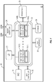
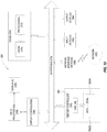
- FIG. 1 is a schematic diagram of an exemplary system-on-a-chip (SoC) 10 that includes a CPU-based system 12.
- the CPU-based system 12 includes a plurality of CPU blocks 14(1)-14(N) in this example, wherein 'N' is equal to any number of CPU blocks 14(1)-14(N) desired.
- each of the CPU blocks 14(1)-14(N) contains two CPUs 16(1), 16(2).
- the CPU blocks 14(1)-14(N) further contain shared Level 2 (L2) caches 18(1)-18(N), respectively.
- a shared Level 3 (L3) cache 20 is also provided for storing cached data that is used by any of, or shared among, each of the CPU blocks 14(1)-14(N).
- An internal system bus 22 is provided to enable each of the CPU blocks 14(1)-14(N) to access the shared L3 cache 20 as well as other shared resources.
- Other shared resources accessed by the CPU blocks 14(1)-14(N) through the internal system bus 22 may include a memory controller 24 for accessing a main, external memory (e.g., double-rate dynamic random access memory (DRAM) (DDR), as a non-limiting example), peripherals 26, other storage 28, an express peripheral component interconnect (PCI) (PCI-e) interface 30, a direct memory access (DMA) controller 32, and/or an integrated memory controller (IMC) 34.
- DRAM double-rate dynamic random access memory
- PCI-e express peripheral component interconnect
- DMA direct memory access
- IMC integrated memory controller
- US 2012/317334 discloses such a controller for compressing/decompressing data to be written/read form a memory.
- the memory capacity requirements of the shared L2 cache 18(1)-18(N) and the shared L3 cache 20, and external memory accessible through the memory controller 24 may also increase.
- Data compression may be employed to increase the effective memory capacity of the CPU-based system 12 without increasing physical memory capacity.
- the use of data compression may increase memory access latency and consume additional memory bandwidth, as multiple memory access requests may be required to retrieve data, depending on whether the data is compressed or uncompressed. Accordingly, it is desirable to increase memory capacity of the CPU-based system 12 using data compression while mitigating the impact on memory access latency and memory bandwidth.
- the invention relates to methods and apparatuses as specified by claims 1-14.
- a CMC comprises a memory interface configured to access a system memory via a system bus.
- the CMC is configured to receive a memory read request comprising a physical address of a memory block to be accessed within a memory line in the system memory.
- the CMC is further configured to read a master directory memory block containing a CI corresponding to the physical address from a master directory in the system memory.
- the CMC is also configured to determine, based on the CI, a number of memory blocks within the memory line in the system memory to read for the memory read request.
- the CMC is additionally configured to read the determined number of memory blocks within the memory line in the system memory beginning at the physical address.
- a CMC comprises a memory interface configured to access a system memory via a system bus.
- the CMC is configured to receive a memory write request comprising write data and a physical address of a memory block to be written within a memory line in the system memory.
- the CMC is further configured to determine a compression pattern for the write data.
- the CMC is also configured to generate a CI for the write data based on the compression pattern.
- the CMC is additionally configured to update a stored CI corresponding to the physical address in a master directory with the generated CI.
- the CMC is further configured to write the write data to one or more memory blocks in the memory line in the system memory based on the generated CI.
- the CMC is also configured to write the generated CI into one or more ECC bits of each of the one or more memory blocks in the memory line of the system memory.
- a method for providing memory bandwidth compression for memory read requests comprises receiving, by a CMC via a system bus, a memory read request comprising a physical address of a memory block to be accessed within a memory line in a system memory.
- the method further comprises reading a master directory memory block containing a CI corresponding to the physical address from a master directory in the system memory.
- the method also comprises determining, based on the CI, a number of memory blocks within the memory line in the system memory to read for the memory read request.
- the method additionally comprises reading the determined number of memory blocks within the memory line in the system memory beginning at the physical address.
- a method for providing memory bandwidth compression for memory write requests comprises receiving, by a CMC via a system bus, a memory write request comprising write data and a physical address of a memory block to be written within a memory line in a system memory.
- the method further comprises determining a compression pattern for the write data.
- the method also comprises generating a CI for the write data based on the compression pattern.
- the method additionally comprises updating a stored CI corresponding to the physical address in a master directory with the generated CI.
- the method further comprises writing the write data to one or more memory blocks in the memory line in the system memory based on the generated CI.
- the method also comprises writing the generated CI into one or more ECC bits of each of the one or more memory blocks in the memory line of the system memory.
- compression methods and formats that may be well-suited for small data block compression are disclosed. These compression methods and formats can be employed for memory bandwidth compression aspects disclosed herein.
- CMCs and compression mechanisms it may be possible to decrease memory access latency and effectively increase memory bandwidth of a CPU-based system, while mitigating an increase in physical memory size and minimizing the impact on system performance.
- a CMC is configured to provide memory bandwidth compression for memory read requests and/or memory write requests.
- the CMC may read a compression indicator (CI) for the physical address from a master directory and/or from error correcting code (ECC) bits associated with the physical address in the system memory.
- the CI in some aspects may provide the CMC with a compression pattern (e.g., indicating whether data is compressed or uncompressed and/or indicating a number of memory blocks in which compressed data is stored at the physical address).
- the CMC determines a number of memory blocks to be read for the memory read request, and reads the determined number of memory blocks beginning at the physical address.
- the CMC may determine a compression pattern for write data to be written, and may generate a CI for the write data based on the compression pattern.
- the CMC may then update the master directory and/or the ECC bits associated with the physical address, and write the write data to the system memory based on the generated CI.
- Some aspects of the CMC may further provide a CI cache for caching previously read CIs. In this manner, the CMC may read and write compressed and uncompressed data more efficiently, resulting in decreased memory access latency and improved system performance.
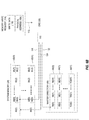
- FIG 2 is a schematic diagram of an SoC 10' that includes an exemplary CPU-based system 12' having a plurality of CPU blocks 14(1)-14(N) similar to the CPU-based system 12 in Figure 1 .
- the CPU-based system 12' in Figure 2 includes some common components with the CPU-based system 12 in Figure 1 , which are noted by common element numbers between Figures 1 and 2 . For the sake of brevity, these elements will not be re-described.
- a CMC 36 is provided in the CPU-based system 12' in Figure 2 .
- the CMC 36 controls access to a system memory 38.
- the system memory 38 may comprise one or more double data rate (DDR) dynamic random access memories (DRAMs) 40(1)-40(R) (referred to hereinafter as "DRAM 40(1)-40(R)"), as a non-limiting example.
- DRAM 40(1)-40(R) double data rate dynamic random access memories
- the CMC 36 in this example employs memory bandwidth compression according to the aspects disclosed herein and below. Similar to the memory controller 24 of the CPU-based system 12 of Figure 1 , the CMC 36 in the CPU-based system 12' in Figure 2 is shared by the CPU blocks 14(1)-14(N) through the internal system bus 22.
- the CMC 36 is provided on a separate semiconductor die 44 from semiconductor dies 46(1), 46(2) that contain the CPU blocks 14(1)-14(N) in Figure 2 .
- the CMC 36 may be included in a common semiconductor die (not shown) with the CPU blocks 14(1)-14(N). Regardless of the die configurations, the CMC 36 is provided such that the CPU blocks 14(1)-14(N) may make memory access requests via the internal system bus 22 to the CMC 36, and receive data from memory through the CMC 36.
- the CMC 36 controls operations for memory accesses to the system memory 38, which is shown in Figures 2 and 3 as comprising DRAM 40(1)-40(R).
- the CMC 36 includes a plurality of memory interfaces (MEM I/Fs) 48(1)-48(P) (e.g., DDR DRAM interfaces) used to service memory access requests (not shown).
- the CMC 36 in this example includes a compression controller 50.
- the compression controller 50 controls compressing data stored to the system memory 38 and decompressing data retrieved from the system memory 38 in response to memory access requests from the CPU blocks 14(1)-14(N) in Figure 2 .
- the CPU blocks 14(1)-14(N) can be provided with a virtual memory address space greater than the actual capacity of memory accessed by the CMC 36.
- the compression controller 50 can also be configured to perform bandwidth compression of information provided over the internal system bus 22 to the CPU blocks 14(1)-14(N).
- the compression controller 50 can perform any number of compression techniques and algorithms to provide memory bandwidth compression.
- a local memory 52 is provided for data structures and other information needed by the compression controller 50 to perform such compression techniques and algorithms.
- the local memory 52 is provided in the form of a static random access memory (SRAM) 54.
- SRAM static random access memory
- the local memory 52 is of sufficient size to be used for data structures and other data storage that may be needed for the compression controller 50 to perform compression techniques and algorithms.
- the local memory 52 may also be partitioned to contain a cache, such as a Level 4 (L4) cache, to provide additional cache memory for internal use within the CMC 36.
- L4 controller 55 may also be provided in the CMC 36 to provide access to the L4 cache.
- Enhanced compression techniques and algorithms may require a larger internal memory, as will be discussed in more detail below.
- the local memory 52 may provide 128 kilobytes (kB) of memory.
- an optional additional internal memory 56 can also be provided for the CMC 36.
- the additional internal memory 56 may be provided as DRAM, as an example.
- the additional internal memory 56 can facilitate additional or greater amounts of storage of data structures and other data than in the local memory 52 for the CMC 36 providing memory compression and decompression mechanisms to increase the memory bandwidth compression of the CPU-based system 12'.
- An internal memory controller 58 is provided in the CMC 36 to control memory accesses to the additional internal memory 56 for use in compression. The internal memory controller 58 is not accessible or viewable to the CPU blocks 14(1)-14(N).
- the CMC 36 in Figure 3 may perform memory bandwidth compression, including, in some aspects, zero-line compression.
- the local memory 52 can be used to store larger data structures used for such compression.
- memory bandwidth compression may reduce memory access latency and allow more CPUs 16(1), 16(2) or their respective threads to access a same number of memory channels while minimizing the impact to memory access latency.
- the number of memory channels may be reduced while achieving similar latency results compared to a greater number of memory channels if such compression was not performed by the CMC 36, which may result in reduced system level power consumption.
- Each of the resources provided for memory bandwidth compression in the CMC 36 in Figure 3 can be used individually or in conjunction with each other to achieve the desired balance among resources and area, power consumption, increased memory capacity through memory capacity compression, and increased performance through memory bandwidth compression.
- Memory bandwidth compression can be enabled or disabled, as desired. Further, the resources described above for use by the CMC 36 can be enabled or disabled to achieve the desired tradeoffs among memory capacity and/or bandwidth compression efficiency, power consumption, and performance. Exemplary memory bandwidth compression techniques using these resources available to the CMC 36 will now be discussed.
- Figure 4 is a schematic diagram of an exemplary memory bandwidth compression mechanism 60 that can be implemented by the CMC 36 of Figure 3 to provide memory bandwidth compression.
- the system memory 38 comprises a plurality of memory lines 62, each of which is associated with a physical address. Each of the plurality of memory lines 62 may be accessed by the CMC 36 using a physical address of a memory read or write request (not shown). Data (not shown) may be stored within each of the memory lines 62 in the system memory 38 in either compressed or uncompressed form. In some aspects, one or more ECC bits comprising a CI 64 may be stored in association with each memory line 62 to indicate whether the memory line 62 is stored in compressed form or not.
- the CMC 36 can check the CI 64 associated with the memory line 62 corresponding to the physical address to be addressed to determine if the memory line 62 is compressed as part of processing of the memory access request.
- a master directory 66 is also provided in the system memory 38.
- the master directory 66 contains one entry 68 per memory line 62 in the system memory 38 corresponding to the physical address.
- the master directory 66 also contains one (1) CI 64 per entry 68 to denote if the memory line 62 is stored as compressed in the memory line 62, and if so, a compression pattern indicating a compression length of data, in aspects in which multiple compression lengths are supported. For example, if the memory line 62 is 128 bytes in length and the data stored therein can be compressed to 64 bytes or less, the CI 64 in the master directory 66 corresponding to the data stored in the system memory 38 may be set to indicate that the data is stored in the first 64 bytes of the 128 byte memory line 62.
- the CMC 36 can compress a memory block to be written into the system memory 38. For example, data (e.g., 128 bytes, or 256 bytes) is compressed. If the compressed data block is smaller than or equal to the memory block size of the system memory 38 (e.g., 64 bytes), then 64 bytes can be written, otherwise 128 bytes are written. 256 bytes could be written as 64, 128, 192, or 256 bytes, depending on the compressed data size.
- the CI 64 stored in one or more ECC bits associated with the memory line 62 in the system memory 38 can also be set to denote if the data at the memory line 62 is compressed or not.
- the CMC 36 can read the CI 64 from the master directory 66 to determine whether the data to be read was compressed in the system memory 38. Based on the CI 64, the CMC 36 can read the data to be accessed from the system memory 38. If the data to be read was compressed in the system memory 38 as indicated by the CI 64, the CMC 36 can read the entire compressed data block with one memory read operation. If the portion of data read was not compressed in the system memory 38, memory access latency may be negatively impacted because the additional portions of the memory line 62 to be read must also be read from the system memory 38.
- a training mechanism may be employed, for a number of address ranges, in which the CMC 36 may be configured to "learn" whether it is better to read the data in two accesses from the system memory 38 in a given set of circumstances, or whether it is better to read the full amount of data from the system memory 38 to avoid the latency impact.
- a CI cache 70 may also be provided in a separate cache outside of the system memory 38.
- the CI cache 70 provides one cache entry 72 per memory line 62 in the system memory 38 to denote if a memory line 62 in the system memory 38 is stored in compressed form or not.
- the CMC 36 can first check the cache entry 72 in the CI cache 70 corresponding to the physical address to be addressed to determine if the memory line 62 at the physical address in the system memory 38 is compressed as part of processing of the memory access request without having to read the memory line 62.
- the CMC 36 does not have to read out the entire memory line 62, thus reducing latency. If the CI cache 70 indicates that the memory line 62 is stored uncompressed, the CMC 36 can read out the entire memory line 62. If a miss occurs in the CI cache 70, the corresponding CI 64 stored in the master directory 66 can be consulted and loaded into the CI cache 70 for subsequent memory access requests to the same physical address.
- the CI cache 70 may be organized as a conventional cache.
- the CI cache 70 may contain a tag array and may be organized as an n-way associative cache, as a non-limiting example.
- the CMC 36 may implement an eviction policy with respect to the CI cache 70.
- each cache line 74 may store multiple cache entries 72.
- Each cache entry 72 may contain a CI 76 to indicate if the memory line 62 in the system memory 38 associated with the cache entry 72 is compressed, and/or to represent a compression pattern indicating compression size for the data corresponding to the cache entry 72.
- the CI 76 may comprise two (2) bits representing four (4) potential compression sizes (e.g., 32, 64, 96, or 128 bytes).
- the CI 64 is redundant, because this information is also stored in the CI 76 in the cache entries 72.
- the CI 76 in the cache entry 72 in the CI cache 70 corresponding to the memory line 62 in the system memory 38 may be set to indicate that the data is stored in the first 64 bytes of a 128 byte memory line 62.
- Figure 5 illustrates an example of an alternative SoC 10" like the SoC 10' in Figure 2 , but the SoC 10" in Figure 5 additionally includes an optional cache 78, which is an L4 cache in this example.
- the CMC 36 can look up a physical address in both the L4 cache 78 and the CI cache 70 concurrently to minimize latency.
- the addresses in the L4 cache 78 are physical addresses that are uncompressed.
- the physical address lookup in the CI cache 70 is redundant.
- a physical address lookup in the CI cache 70 is required to obtain the data from the system memory 38.
- the L4 cache 78 and the CI cache 70 may be primed.
- Figures 6A and 6B are provided to illustrate exemplary communications flows and exemplary elements of the system memory 38 and the master directory 66 of Figure 4 that may be accessed by the CMC 36 of Figure 3 for providing memory bandwidth compression.
- Figure 6A illustrates exemplary communications flows during a memory read operation
- Figure 6B illustrates exemplary communications flows during a memory write operation, respectively.
- elements of Figures 3 and 4 are referenced for the sake of clarity.
- the system memory 38 includes a plurality of memory lines 80(0)-80(X) for storing compressed and uncompressed data.
- the memory lines 80(0)-80(X) are each subdivided into respective memory blocks 82(0)-82(Z) and 84(0)-84(Z), as determined by an underlying memory architecture of the system memory 38.
- the size of each of the memory blocks 82(0)-82(Z), 84(0)-84(Z) represents a smallest amount of data that may be read from the system memory 38 in a memory read operation.
- each of the memory lines 80(0)-80(X) may comprise 128 bytes of data, subdivided into two 64-byte memory blocks 82(0)-82(Z), 84(0)-84(Z).
- each of the memory lines 80(0)-80(X) may comprise more or fewer bytes of data (e.g., 256 bytes or 64 bytes, as non-limiting examples).
- the memory blocks 82(0)-82(Z), 84(0)-84(Z) within the memory lines 80(0)-80(X) may be larger or smaller (e.g., 128 bytes or 32 bytes, as non-limiting examples).
- a memory read operation may read fewer bytes than the size of each of the memory blocks 82(0)-82(Z), 84(0)-84(Z), but still consume the same amount of memory bandwidth as one of the memory blocks 82(0)-82(Z), 84(0)-84(Z).
- Each of the memory blocks 82(0)-82(Z), 84(0)-84(Z) is associated with one or more corresponding ECC bits 86(0)-86(Z), 88(0)-88(Z).
- ECC bits such as the ECC bits 86(0)-86(Z), 88(0)-88(Z) are used conventionally to detect and correct commonly encountered types of internal data corruption within the memory blocks 82(0)-82(Z), 84(0)-84(Z).
- one or more of the ECC bits 86(0)-86(Z), 88(0)-88(Z) are repurposed to store CIs 90(0)-90(Z), 92(0)-92(Z) for the respective memory blocks 82(0)-82(Z), 84(0)-84(Z).
- ECC bits 86(0)-86(Z), 88(0)-88(Z) in Figures 6A and 6B are depicted as being adjacent to their respective memory blocks 82(0)-82(Z), 84(0)-84(Z), it is to be understood that the ECC bits 86(0)-86(Z), 88(0)-88(Z) may be located elsewhere within the system memory 38.
- the system memory 38 also includes the master directory 66, which includes multiple master directory memory blocks 94(0)-94(Y). Each of the master directory memory blocks 94(0)-94(Y) is the same size as the memory blocks 82(0)-82(Z), 84(0)-84(Z).
- the master directory memory blocks 94(0)-94(Y) store CIs 96(0)-96(W), 98(0)-98(W), 100(0)-100(W), each of which corresponds to a physical address of one of the memory blocks 82(0)-82(Z), 84(0)-84(Z).
- the CIs 90(0)-90(Z), 92(0)-92(Z) stored in the ECC bits 86(0)-86(Z), 88(0)-88(Z) and the CIs 96(0)-96(W), 98(0)-98(W), 100(0)-100(W) stored in the master directory memory blocks 94(0)-94(Y) may be maintained so as to always store the same value for a given one of the memory blocks 82(0)-82(Z), 84(0)-84(Z).
- Some aspects may provide that the CIs 90(0)-90(Z), 92(0)-92(Z) stored in the ECC bits 86(0)-86(Z), 88(0)-88(Z) may be updated more frequently than the CIs 96(0)-96(W), 98(0)-98(W), 100(0)-100(W) in the master directory memory blocks 94(0)-94(Y).
- the CIs 90(0)-90(Z), 92(0)-92(Z) and the CIs 96(0)-96(W), 98(0)-98(W), 100(0)-100(W) each may comprise one or more bits that indicate a compression status of data stored at a corresponding memory block 82(0)-82(Z), 84(0)-84(Z) of the system memory 38.
- each of the CIs 90(0)-90(Z), 92(0)-92(Z) and the CIs 96(0)-96(W), 98(0)-98(W), 100(0)-100(W) may comprise a single bit indicating whether data in the corresponding memory block 82(0)-82(Z), 84(0)-84(Z) is compressed or uncompressed.
- each of the CIs 90(0)-90(Z), 92(0)-92(Z) and the CIs 96(0)-96(W), 98(0)-98(W), 100(0)-100(W) may comprise multiple bits that may be used to indicate a compression pattern (e.g., a number of the memory blocks 82(0)-82(Z), 84(0)-84(Z) occupied by the compressed data, as a non-limiting example) for each of the corresponding memory blocks 82(0)-82(Z), 84(0)-84(Z).
- a compression pattern e.g., a number of the memory blocks 82(0)-82(Z), 84(0)-84(Z) occupied by the compressed data, as a non-limiting example
- a memory read request 102 specifying a physical address 104 is received by the CMC 36, as indicated by arrow 106.
- the physical address 104 corresponds to the memory block 82(0), which is a 64-byte subdivision of the 128-byte memory line 80(0).
- the CMC 36 is unaware of whether the data stored at the memory block 82(0) is compressed or not. The CMC 36 could proceed with reading the entire memory line 80(0), but if the requested data is stored in compressed form in only the memory block 82(0), a read of the memory block 82(Z) would be unnecessary, and would result in increased memory access latency.
- the CMC 36 could read only memory block 82(0), determine based on its contents whether the data stored therein is compressed or not, and then read the memory block 82(Z) if the data is uncompressed.
- this approach may also result in increased memory access latency resulting from issuing the two separate memory read operations.
- the CMC 36 risks executing unnecessary memory read operations that may negatively impact memory access latency.
- the CMC 36 may determine how many memory blocks 82(0)-82(Z) should be read to ensure that all data (compressed or uncompressed) for a given memory read request 102 is efficiently read from the system memory 38.
- the CMC 36 may read the master directory memory block 94(0) of the master directory 66 to access the CI 96(0) corresponding to the physical address 104 of the memory block 82(0), as indicated by arrow 108.
- the CI 96(0) may then be used by the CMC 36 to determine how many memory blocks 82(0)-82(Z) within the memory line 80(0) to read to ensure that the data requested by the memory read request 102 is efficiently retrieved.
- the CMC 36 may determine how many memory blocks 82(0)-82(X) to read by determining a compression pattern (not shown) indicated by the CI 96(0).
- the CI 96(0) may be a single bit indicating that data is compressed (i.e., only the memory block 82(0) should be read) or uncompressed (i.e., both the memory blocks 82(0) and 82(Z) should be read).
- the memory lines 80(0)-80(X) of the system memory 38 each contain more than two memory blocks 82(0)-82(Z), 84(0)-84(Z)
- the CI 96(0) may comprise multiple bits indicating how many memory blocks 82(0)-82(Z) contain compressed data.
- the CI 96(0) may indicate that compressed data is stored in 64 bytes, 128 bytes, or 192 bytes (corresponding to the memory block 82(0), the memory blocks 82(0)-82(1), and the memory blocks 82(0)-82(2), respectively). Based on the CI 96(0), the CMC 36 may then issue an appropriate number of memory read operations to read the determined number of memory blocks 82(0)-82(Z) within the memory line 80(0), as indicated by arrow 110.
- the CMC 36 may determine that the compression pattern indicated by the CI 96(0) comprises a zero-line indicator, which indicates to the CMC 36 that data stored at the physical address 104 is made up entirely of zero values. In such case, the CMC 36 may read zero memory blocks 82(0)-82(Z). According to some aspects, the CMC 36 may determine that the compression pattern indicated by the CI 96(0) comprises an indicator of other fixed data patterns stored at the physical address 104 (such as all ones (Is), as a non-limiting example).
- Is all ones
- the CMC 36 may probabilistically determine (e.g., based on a random number generator (not shown)) whether to read the CI 96(0) for the memory block 82(0) from the master directory 66, or alternatively whether to read the CI 90(0) for the memory block 82(0) from the ECC bits 86(0). In the latter case, the CMC 36 may read the CI 90(0), as indicated by dashed arrow 112, and use the CI 90(0) in determining how many memory blocks 82(0)-82(Z) to read from the memory line 80(0).
- the CMC 36 receives a memory write request 114, as indicated by arrow 116.
- the memory write request 114 includes both write data 118 to be written to the system memory 38, as well as the physical address 104 of the system memory 38 to which the write data 118 is to be written. For purposes of illustration, it is again assumed that the physical address 104 corresponds to the memory block 82(0).
- the CMC 36 may carry out operations to compress the write data 118, and based on the results of compressing the write data 118, may determine a compression pattern for the write data 118.
- the compression pattern may indicate, as non-limiting examples, whether or not the write data 118 was successfully compressed, and/or a number of memory blocks 82(0)-82(Z) occupied by the compressed write data 118. Based on the compression pattern, the CMC 36 generates a CI 120 for the write data 118.
- the CMC 36 may then update the CI 96(0) stored in the master directory 66 for the physical address 104 of the memory block 82(0) with the generated CI 120, as indicated by arrow 122.
- the master directory 66 may be updated for only a certain percentage of memory write requests 114 received by the CMC 36.
- the master directory 66 may only be updated for ten percent (10%) of memory write requests 114 received by the CMC 36.
- the CMC 36 may probabilistically determine (e.g., based on a random number generator (not shown)) whether to update the stored CI 96(0) for the memory block 82(0) in the master directory 66. If not, this operation may be omitted.
- the CMC 36 then writes the write data 118 to one or more of the memory blocks 82(0)-82(Z), as indicated by arrow 124.
- the CMC 36 also writes the generated CI 120 into the CIs 90(0)-90(Z) stored in the ECC bits 86(0)-86(Z) of the one or more memory blocks 82(0)-82(Z) to which the write data 118 was written, as indicated by arrow 126.
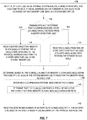
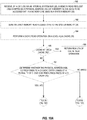
- FIG 7 is a flowchart that illustrates exemplary operations for performing a memory read operation by the CMC 36 of Figure 3 using memory bandwidth compression, as discussed with respect to Figure 6A .
- operations begin with the CMC 36 receiving, via the internal system bus 22, the memory read request 102 comprising the physical address 104 of the memory block 82(0) to be accessed within the memory line 80(0) in the system memory 38 (block 128).
- the CMC 36 optionally may probabilistically determine whether the CI 96(0) should be read from the master directory 66 (block 130).
- the CMC 36 determines that the CI 96(0) should not be read from the master directory 66, the CMC 36 reads the CI 90(0) from the one or more ECC bits 86(0) along with reading the memory block 82(0), and uses the CI 90(0) as the CI 96(0) (block 132). However, if the CMC 36 is not using probabilistic determination, or if the CMC 36 probabilistically determines at decision block 130 that the CI 96(0) should be read from the master directory 66, the CMC 36 reads the master directory memory block 94(0) containing the CI 96(0) corresponding to the physical address 104 from the master directory 66 in the system memory 38 (block 134).
- the CMC 36 determines, based on the CI 96(0), a number of memory blocks 82(0)-82(Z) within the memory line 80(0) in the system memory 38 to read for the memory read request 102 (block 136).
- the operations of block 136 for determining the number of memory blocks 82(0)-82(Z) to read may comprise determining a compression pattern indicated by the CI 96(0) (block 138).
- the CMC 36 may determine that the CI 96(0) comprises a zero-line indicator indicating that zero memory blocks 82(0)-82(Z) should be read (block 140).
- the CMC 36 then reads the determined number of memory blocks 82(0)-82(Z) within the memory line 80(0) in the system memory 38 beginning at the physical address 104 (block 142).
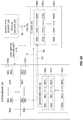
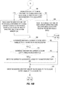
- Figure 8 is provided.
- elements of Figures 2 , 3 , and 6B are referenced in describing Figure 8 for the sake of clarity. Operations in Figure 8 begin with the CMC 36 receiving, via the internal system bus 22, the memory write request 114 comprising the write data 118 and the physical address 104 of the memory block 82(0) to be written within the memory line 80(0) in the system memory 38 (block 144).
- the CMC 36 After attempting to compress the write data 118, the CMC 36 determines a compression pattern for the write data 118 (e.g., whether the write data 118 was compressed, and/or how many memory blocks 82(0)-82(Z) are required to store the write data 118) (block 146). Based on the compression pattern, the CMC 36 generates a CI 120 for the write data 118 based on the compression pattern (block 148).
- a compression pattern for the write data 118 e.g., whether the write data 118 was compressed, and/or how many memory blocks 82(0)-82(Z) are required to store the write data 118.
- the CMC 36 optionally may probabilistically determine whether the CI 96(0) stored in the master directory 66 should be updated (block 150). If the CMC 36 determines that the stored CI 96(0) in the master directory 66 should not be updated, processing resumes at block 152 of Figure 8 . However, if the CMC 36 determines at decision block 150 that the stored CI 96(0) in the master directory 66 should be updated, or if the CMC 36 is not employing probabilistic determination, the CMC 36 updates the stored CI 96(0) corresponding to the physical address 104 in the master directory 66 with the generated CI 120 (block 154).
- the CMC 36 next writes the write data 118 to one or more of the memory blocks 82(0)-82(Z) in the memory line 80(0) in the system memory 38 based on the generated CI 120 (block 152).
- the CMC 36 also writes the generated CI 120 into one or more ECC bits 86(0)-86(Z) of each of the memory blocks 82(0)-82(Z) in the memory line 80(0) of the system memory 38 (block 156).
- the generated CI 120 is written into the ECC bits 86(0) as part of the same memory write operation that writes the write data 118 to the first memory block 82(0).
- FIGS 9A and 9B are provided to illustrate exemplary communications flows and exemplary elements of the CI cache 70 that may be accessed by the CMC 36 of Figure 3 for providing memory bandwidth compression.
- Figures 9A and 9B illustrate exemplary communications flows during a memory read operation and a memory write operation, respectively, using the CI cache 70.
- elements of Figures 3 , 4 , 6A , and 6B are referenced for the sake of clarity.
- the CI cache 70 of the CMC 36 includes multiple CI cache entries 158(0)-158(T) storing cached CIs 160(0)-160(W), 162(0)-162(W), and 164(0)-164(W).
- Each of the cache entries 158(0)-158(T) is the same size as the master directory memory blocks 94(0)-94(Y), and in some aspects are configured to store one of the master directory memory blocks 94(0)-94(Y) that is read in the course of a memory read operation or a memory write operation by the CMC 36.
- the CMC 36 may access the cached CIs 160(0)-160(W), 162(0)-162(W), and 164(0)-164(W) on subsequent memory read operations and memory write operations, rather than having to access the system memory 38 to read the CIs 90(0)-90(Z), 92(0)-92(Z) and/or the CIs 96(0)-96(W), 98(0)-98(W), 100(0)-100(W). Because the CMC 36 may read from and write to the CI cache 70 much faster than reading from and writing to the system memory 38, the use of the CI cache 70 may enable the CMC 36 to further decrease memory access latency.
- the CMC 36 providing the CI cache 70 receives the memory read request 102 comprising the physical address 104, as indicated by arrow 166. It is assumed that the physical address 104 corresponds to the memory block 82(0) of the memory line 80(0) of the system memory 38. The CMC 36 may then determine whether the physical address 104 corresponds to one of the CI cache entries 158(0)-158(T).
- the CMC 36 If one of the CI cache entries 158(0)-158(T), such as the CI cache entry 158(0), corresponds to the physical address 104 of the memory block 82(0) (i.e., a cache "hit"), then the CMC 36 has identified the CI cache entry 158(0) that includes a CI indicator, such as the CI 160(0), for the memory block 82(0). The CMC 36 then reads the CI 160(0) from the CI cache entry 158(0) of the CI cache 70, and determines a number of memory blocks 82(0)-82(Z) to read based on the CI 160(0) as discussed above with respect to Figure 6A .
- the CMC 36 may read the master directory memory block 94(0) of the master directory 66 to access the CI 96(0) corresponding to the physical address 104 of the memory block 82(0), as indicated by arrow 168. As noted above, in some aspects it may be desirable for the CMC 36 to read the master directory 66 for only a certain percentage of memory read requests 102 received by the CMC 36.
- the CMC 36 may probabilistically determine (e.g., based on a random number generator (not shown)) whether to read the master directory memory block 94(0) from the master directory 66, or alternatively to read the CI 90(0) for the memory block 82(0) from the ECC bits 86(0). In the latter case, the CMC 36 may read the CI 90(0), as indicated by dashed arrow 170. The CMC 36 may then use the CI 90(0) without further updating the CI cache 70.
- a random number generator not shown
- the CMC 36 may then write the master directory memory block 94(0) into the CI cache 70 as a new CI cache entry 158(0).
- the CI cache 70 may first determine whether a current CI cache entry 158(0) must be evicted. If so, the CI cache 70 may further determine whether the current CI cache entry 158(0) has been modified since being written into the CI cache 70 (e.g., by determining whether at least one cached CI 160(0)-160(W) has been changed since being read from the master directory 66).
- the CI cache 70 may determine whether the current CI cache entry 158(0) has been modified by checking to see if a dirty bit (not shown) associated with the current CI cache entry 158(0) has been set. If the current CI cache entry 158(0) has been modified, the CMC 36 writes the current CI cache entry 158(0) to the corresponding one of the master directory memory blocks 94(0)-94(Y). The CMC 36 then reads the CI 160(0) from the CI cache entry 158(0) of the CI cache 70, and determines a number of memory blocks 82(0)-82(Z) to read based on the CI 160(0) as discussed above. The determined number of memory blocks 82(0)-82(Z) are then read by the CMC 36, as indicated by arrow 172.
- the CMC 36 may issue an early memory read request 174, based on the memory read request 102, to the system memory 38 concurrently with determining whether the physical address 104 corresponds to one of the CI cache entries 158(0)-158(T).
- the early memory read request 174 may be processed in parallel with the CMC 36 determining the number of memory blocks 82(0)-82(Z) to read based on the CI 160(0).
- the early memory read request 174 may be modified based on the CI 160(0).
- the early memory read request 174 may be modified to read the determined number of memory blocks 82(0)-82(Z). In this manner, additional memory bandwidth compression and decreased memory access latency may be provided through parallel processing of the early memory read request 174 and the CI cache 70 reads and/or writes.
- the CMC 36 may also perform a cache read operation (not shown) to look up the physical address 104 in the L4 cache 78 concurrently with determining whether the physical address 104 corresponds to one of the CI cache entries 158(0)-158(T) in the CI cache 70. By doing so, the CMC 36 may further minimize memory access latency.
- the CMC 36 receives the memory write request 114, as indicated by arrow 176.
- the memory write request 114 includes both the write data 118 to be written to the system memory 38, as well as the physical address 104 of the system memory 38 to which the write data 118 is to be written. It is again assumed for purposes of illustration that the physical address 104 corresponds to the memory block 82(0).
- the CMC 36 may carry out operations to compress the write data 118, and based on the results of compressing the write data 118, may determine a compression pattern for the write data 118.
- the compression pattern may indicate, as non-limiting examples, whether or not the write data 118 was successfully compressed, and/or a number of memory blocks 82(0)-82(Z) occupied by the compressed write data 118. Based on the compression pattern, the CMC 36 generates the CI 120 for the write data 118.
- the CMC 36 may then determine whether the physical address 104 corresponds to one of the CI cache entries 158(0)-158(T). If one of the CI cache entries 158(0)-158(T), such as the CI cache entry 158(0), corresponds to the physical address 104 of the memory block 82(0) (i.e., a cache "hit"), then the CMC 36 has identified the CI cache entry 158(0) that includes a CI indicator, such as the CI 160(0), for the memory block 82(0). Accordingly, the CMC 36 updates the CI 160(0) of the CI cache entry 158(0) with the generated CI 120, as indicated by arrow 178.
- the CMC 36 next writes the write data 118 to one or more of the memory blocks 82(0)-82(Z) in the memory line 80(0), as indicated by arrow 180.
- the CMC 36 also writes the generated CI 120 into one or more of the ECC bits 86(0)-86(Z) of the one or more of the memory blocks 82(0)-82(Z) to which the write data 118 was written, as indicated by arrow 182.
- the generated CI 120 is written into the ECC bits 86(0) as part of the same memory write operation that writes the write data 118 to the first memory block 82(0).
- the CMC 36 may update the stored CI 96(0) corresponding to the physical address 104 in the master directory 66 with the generated CI 120, as indicated by arrow 184.
- the CMC 36 may then write the master directory memory block 94(0) into the CI cache 70 as a new CI cache entry 158(0), as indicated by arrow 186.
- the CI cache 70 may first determine whether a current CI cache entry 158(0) must be evicted.
- the CI cache 70 may further determine whether the current CI cache entry 158(0) has been modified since being written into the CI cache 70. In some aspects, the CI cache 70 may determine whether the current CI cache entry 158(0) has been modified by checking to see if a dirty bit (not shown) associated with the CI cache entry 158(0) has been set. If the current CI cache entry 158(0) has been modified, the CMC 36 writes the current CI cache entry 158(0) to the corresponding one of the master directory memory blocks 94(0)-94(Y), as indicated by arrow 188, before writing the master directory memory block 94(0) into the CI cache 70 as the new CI cache entry 158(0).
- the master directory 66 may be updated in response to a cache miss in the CI cache 70 for only a certain percentage of memory write requests 114 received by the CMC 36. Accordingly, in such aspects, the CMC 36 may probabilistically determine (e.g., based on a random number generator (not shown)) whether to update the stored CI 96(0) for the memory block 82(0) in the master directory 66. If not, the operations described above with respect to a cache miss are omitted (i.e., neither the master directory 66 nor the CI cache 70 are updated, and the generated CI 120 is stored in the ECC bits 86(0)-86(Z) of one or more of the memory blocks 82(0)-82(Z)).
- Figures 10A-10C are flowcharts illustrating exemplary operations for performing a memory read operation by the CMC 36 of Figure 3 using the CI cache 70 of Figures 9A and 9B .
- Figure 10A illustrates operations for receiving the memory read request 102 and determining whether a search of the CI cache 70 for a CI 160(0) corresponding to the physical address 104 of the memory read request 102 results in a hit or a miss.
- Figure 10B illustrates operations carried out as a result of a cache miss on the CI cache 70
- Figure 10C illustrates operations carried out as a result of a cache hit on the CI cache 70.
- Elements of Figures 2 , 3 , and 9A are referenced in describing Figures 10A-10C for the sake of clarity.
- Operations in Figure 10A begin with the CMC 36 receiving, via the internal system bus 22, the memory read request 102 comprising the physical address 104 of a memory block 82(0) to be accessed within the memory line 80(0) in the system memory 38 (block 190).
- the CMC 36 may send the early memory read request 174 to the system memory 38 concurrently with subsequent operations (block 192).
- the CMC 36 may perform a cache read operation on an L4 cache, such as the L4 cache 78 of Figure 5 , concurrently with subsequent operations (block 194).
- a determination is then made regarding whether the cache read operation on the L4 cache 78 resulted in a cache hit (block 195). If so, then the results of the cache read operation are returned, and the read to the system memory 38 is rendered moot (block 196).
- the CMC 36 next determines whether the physical address 104 corresponds to a CI cache entry 158(0) of a plurality of CI cache entries 158(0)-158(T) of a CI cache 70 (block 197). If the CMC 36 determines at decision block 196 that the physical address 104 does not correspond to a CI cache entry 158(0) of the plurality of CI cache entries 158(0)-158(T) (i.e., a cache miss), processing resumes at block 198 of Figure 10B . If the physical address 104 is determined to correspond to a CI cache entry 158(0) (i.e., a cache hit), processing resumes at block 200 of Figure 10C .
- the CMC 36 in some aspects may probabilistically determine whether the CI 96(0) should be read from the master directory 66 in response to a cache miss (block 198).
- the ECC bits 86(0)-86(Z), 88(0)-88(Z) of the one or more of the memory blocks 82(0)-82(Z), 84(0)-84(Z) will store the CIs 90(0)-90(Z), 92(0)-92(Z).
- the probabilistic determination may be made using a random number generator, as a non-limiting example.
- the CMC 36 If it is determined at decision block 198 that the CI 96(0) should be read from the master directory 66, the CMC 36 reads the master directory memory block 94(0) containing the CI 96(0) corresponding to the physical address 104 from the master directory 66 in the system memory 38 (block 202). If the CMC 36 determines at decision block 198 that the CI 96(0) should not be read from the master directory 66, the CMC 36 reads the CI 90(0) from one or more ECC bits 86(0) along with reading the memory block 82(0) (block 204). Processing then resumes at block 214 of Figure 10C .
- the CMC 36 may next determine whether a current CI cache entry 158(0) of the CI cache 70 should be evicted (block 206). If not, processing resumes at block 208 of Figure 10B . If the CMC 36 determines at decision block 206 that the current CI cache entry 158(0) should be evicted, the CMC 36 next determines whether the current CI cache entry 158(0) has been modified (block 210). This determination may be based on determining whether a dirty bit for the CI cache entry 158(0) has been set, as a non-limiting example. If the current CI cache entry 158(0) is determined at decision block 210 to be unchanged, processing resumes at block 208 of Figure 10B .
- the CMC 36 writes the current CI cache entry 158(0) to the master directory 66 (block 212).
- the master directory memory block 94(0) is then written to the CI cache entry 158(0) of the CI cache 70 (block 208). Processing then resumes at block 200 of Figure 10C .
- the CMC 36 reads the CI 160(0) from the CI cache entry 158(0) of the CI cache 70 (block 200).
- the CMC 36 next determines, based on the CI 160(0), a number of memory blocks 82(0)-82(Z) within the memory line 80(0) in the system memory 38 to read for the memory read request 102 (block 214).
- the CMC 36 then reads the determined number of memory blocks 82(0)-82(Z) within the memory line 80(0) in the system memory 38 beginning at the physical address 104 (block 216).
- the operations of block 216 for reading the determined number of memory blocks 82(0)-82(Z) may include modifying the early memory read request 174 based on the CI 160(0) (block 218).
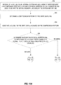
- Figures 11A-11C are provided.
- Figure 11A illustrates operations for receiving the memory write request 114 and determining whether a search of the CI cache 70 for a CI cache entry 158(0)-158(T) corresponding to the physical address 104 of the memory write request 114 results in a hit or a miss.
- Figure 11B illustrates operations carried out as a result of a cache miss on the CI cache 70
- Figure 11C illustrates operations carried out as a result of a cache hit on the CI cache 70.
- Elements of Figures 2 , 3 , and 9B are referenced in describing Figures 11A-11C for the sake of clarity.
- FIG 11A operations begin with the CMC 36, via the internal system bus 22, a memory write request 114 comprising write data 118 and the physical address 104 of the memory block 82(0) to be written within the memory line 80(0) in the system memory 38 (block 220).
- the CMC 36 determines a compression pattern for the write data 118 (block 222).
- the compression pattern may indicate whether the write data 118 is compressed or uncompressed, and/or a number of memory blocks 82(0)-82(Z) occupied by the write data 118.
- the CMC 36 Based on the compression pattern, the CMC 36 generates a CI 120 for the write data 118 based on the compression pattern (block 224).
- the CMC 36 next determines whether the physical address 104 corresponds to a CI cache entry 158(0) of a plurality of CI cache entries 158(0)-158(T) of a CI cache 70 (block 226). If the physical address 104 is determined at decision block 226 not to correspond to a CI cache entry 158(0) of the plurality of CI cache entries 158(0)-158(T) (i.e., a cache miss), processing resumes at block 228 of Figure 11B . However, if the CMC 36 determines at decision block 226 that the physical address 104 corresponds to a CI cache entry 158(0) (i.e., a cache hit), processing resumes at block 230 of Figure 11C .
- some aspects of the CMC 36 may probabilistically determine whether the CI 96(0) should be updated in the master directory 66 (block 228). If it is determined at decision block 228 that the CI 96(0) should not be updated, processing resumes at block 242 of Figure 11C . However, if the CMC 36 determines at decision block 228 to update the CI 96(0), or if the CMC 36 is not configured to use probabilistic determination, the CMC 36 updates the stored CI 96(0) corresponding to the physical address 104 in the master directory 66 with the generated CI 120 (block 232).
- the CMC 36 may next determine whether a current CI cache entry 158(0) of the CI cache 70 should be evicted (block 234). If not, processing resumes at block 236 of Figure 11B . If the CMC 36 determines at decision block 234 that the current CI cache entry 158(0) should be evicted, the CMC 36 determines whether the current CI cache entry 158(0) has been modified (block 238). Determining whether the CI cache entry 158(0) has been modified may comprise determining whether a dirty bit of the CI cache entry 158(0) has been set, as a non-limiting example. If the current CI cache entry 158(0) is determined at decision block 238 to be unchanged, processing resumes at block 236 of Figure 11B .
- the CMC 36 determines at decision block 238 that the current CI cache entry 158(0) has been modified, the CMC 36 writes the current CI cache entry 158(0) to the master directory 66 (block 240). The CMC 36 then writes the stored CI 96(0) to the CI cache entry 158(0) of the CI cache 70 (block 236). Processing resumes at block 242 of Figure 11C .
- the CMC 36 updates the CI cache entry 158(0) of the CI cache 70 with the generated CI 120 (block 230).
- the CMC 36 then writes the write data 118 to one or more memory blocks 82(0)-82(Z) in the memory line 80(0) in the system memory 38 based on the generated CI 120 (block 242).
- the generated CI 120 is written into one or more ECC bits 86(0)-86(Z) of each of the one or more memory blocks 82(0)-82(Z) in the memory line 80(0) of the system memory 38 (block 244).
- the generated CI 120 is written into the ECC bits 86(0) as part of the same memory write operation that writes the write data 118 to the first memory block 82(0).
- a memory data block 82(0)-82(Z) having a configurable fixed data pattern may be desired to provide compression of a memory data block 82(0)-82(Z) having a configurable fixed data pattern as a special case to optimize compression. For example, if a memory data block 82(0)-82(Z) (e.g., 128 bytes) is all 0's, then data is not read or written, but noted in a separate data structure as all 0's. A zero-bit could be provided in the system memory 38 to denote if a memory line 80(0)-80(X) is compressed, thus adding one (1) bit per memory data block 82(0)-82(Z).
- a memory data block 82(0)-82(Z) e.g., 128 bytes
- a zero-bit could be provided in the system memory 38 to denote if a memory line 80(0)-80(X) is compressed, thus adding one (1) bit per memory data block 82(0)-82(Z).
- the CMC 36 could maintain a cache that remembers, for a number of 128-byte memory blocks 82(0)-82(Z) for example, if a block is all 0's. For a write operation, if a line of a memory data block 82(0)-82(Z) is all 0's, the CMC 36 does not write the line to the system memory 38, but the CI cache 70 is updated. For a read operation, the zero-bit in the CI cache 70 is checked for the line. If the line is in the CI cache 70, then depending on the zero-bit, either the line is read from the system memory 38, or all 0's is returned. If the line is not in the CI cache 70, then it is read from the system memory 38. If the line is zero, then the CI cache 70 can be updated.
- the CI cache 70 can be updated to evict a cache line 74 according to known techniques (LRU, pseudo-LRU, etc.). If a line is evicted, all lines that have their zero-bit set need to be written to main memory. This can be organized as a write-all-zeros queue. A possible optimization would be to use two (2) bits, wherein one bit denotes if the line is all-zeros, and another bit denotes if the line is dirty (i.e., has not been written to main memory yet). A background task of the CMC 36 can inspect the CI cache 70 and queue the lines with dirty-bits in a "write-all-zeros" queue.
- different memory compression mechanisms can be employed by the CMC 36 as desired. For example, it may be desired to employ memory compression mechanisms that are optimized for small data blocks, such as 64, 128, and 256 bytes, since the cache lines 74 described in the examples above include these sizes as examples.
- a value of a CI comprising multiple bits may indicate a compression status and/or a fixed data pattern stored in a memory block such as one of the memory blocks 82(0)-82(Z).
- a value of "00" may indicate that the corresponding memory block is uncompressed, while a value of "01” may indicate that the corresponding memory block is compressed.
- a value of "11” may indicate that a fixed pattern (e.g., all zeroes (0s) or all ones (Is)) is stored in the corresponding memory block.
- the master directory 66 would always be updated rather than being updated subject to a probabilistic determination.
- Figure 12 illustrates a frequent pattern compression data compression mechanism 246.
- the source data in a source data format 248 to be compressed is shown by example as 128 bytes.
- a compressed data format 250 is shown below.
- the compressed data format 250 is provided in a format of prefix codes Px and data behind the prefix as Datax.
- the prefix is 3-bits.
- the prefix codes are shown in a prefix code column 252 in a frequent pattern encoding table 254 that shows the pattern encoded in a pattern encoded column 256 for a given prefix code in the prefix code column 252.
- the data size for the pattern encoded is provided in a data size column 258 of the frequent pattern encoding table 254.
- Figure 13 illustrates a 32-bit frequent pattern compression data compression mechanism 260.
- the source data in a source data format 262 to be compressed is shown by example as 128 bytes.
- a compressed data format 264 is shown below.
- the compressed data format 264 is provided in a format of prefix Px and data immediately behind the prefix as Datax.
- a new compressed data format 266 is provided in a different format of prefix codes Px, data Datax, flags, and patterns, which are organized to be grouped together for efficiency purposes.
- the prefix code is 3-bits.
- the prefix codes are shown in a prefix code column 268 in a frequency pattern encoding table 270 that shows the pattern encoded in a pattern encoded column 272 for a given prefix code in the prefix code column 268.
- the data size for the pattern encoded is provided in a data size column 274 of the frequency pattern encoding table 270.
- the prefix code 000 signifies an uncompressed pattern, which would be data of the full size of 32-bits in the new compressed data format 266.
- the prefix code 001 signifies an all zero data block, which can be provided as 0 bits in the data of the new compressed data format 266.
- prefix codes 010-111 can be used to encode other specific patterns that are recognized in the source data, which in this example are patterns in 0, 4, 8, 12, 16, and 24 bits respectively.
- Figure 14 illustrates an example of 32-bit frequent pattern compression data compression mechanism 276.
- the source data in a source data format 278 to be compressed is shown by example as 128 bytes.
- a compressed data format 280 is shown below.
- the compressed data format 280 is provided in a format of prefix Px and data behind the prefix as Datax.
- a new compressed data format 282 is provided in a different format of prefix codes Px, data Datax, flags, and patterns, which are organized to be grouped together for efficiency purposes.
- the prefix code is 3-bits.
- the prefix codes are shown in a prefix code column 284 in a frequency pattern encoding table 286 that shows the pattern encoded in a pattern encoded column 288 for a given prefix code in the prefix code column 284.
- the data size for the pattern encoded is provided in a data size column 290 of the frequency pattern encoding table 286.
- the prefix code 000 signifies an uncompressed pattern, which would be data of the full size of 32-bits in the new compressed data format 282.
- the prefix code 001 signifies an all zero data block, which can be provided as 0 bits in the data of the new compressed data format 282.
- Prefix code 010 signifies pattern 0xFFFFFFFF, which is a specific pattern and thus requires 0-bit data size in the compressed data according to the new compressed data format 282.
- Other patterns are shown in the frequency pattern encoding table 286 for prefix codes 011-111.
- the flags field in the new compressed data format 282 indicates which patterns for prefix codes 001-111 are present in the data portions (i.e., Datax) of the compressed data. If the pattern is present in the compressed data, the patterns are stored in the new compressed data format 282 that can then be consulted to recreate the uncompressed data.
- the data fields include the compressed data according to the prefix code associated with the data field in the new compressed data format 282.
- Figure 15 illustrates another example of 64-bit frequent pattern compression data compression mechanism 292.
- the source data in a source data format 294 to be compressed is shown by example as 128 bytes.
- a new compressed data format 296 is provided in a different format of prefix codes Px, data Datax, flags, and patterns, which are organized to be grouped together for efficiency purposes.
- the prefix code is 4-bits.
- the prefix codes are shown in prefix code columns 298, 300 in a frequency pattern encoding table 302 that shows the pattern encoded in pattern encoded columns 304, 306 for a given prefix code in the prefix code columns 298, 300.
- the data size for the pattern encoded is provided in data size columns 308, 310 of the frequency pattern encoding table 302.
- the prefix code 0000 signifies an all zero data block, which can be provided as 0 bits in the data of the new compressed data format 296.
- Other patterns are shown in the frequency pattern encoding table 302 for prefix codes 0001-1111, which include ASCII patterns for frequently occurring ASCII patterns.
- the flags field in the new compressed data format 296 indicates which patterns for prefix codes 0001-1111 are present in the data portions (i.e., Datax) compressed data. If the pattern is present in the compressed data, the patterns are stored in the new compressed data format 296 that can then be consulted to recreate the uncompressed data.
- the data fields include the compressed data according to the prefix code associated with the data field in the new compressed data format 296.
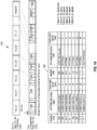
- Figure 16 illustrates another example of 64-bit frequent pattern compression data compression mechanism 312.
- the source data in a source data format 314 to be compressed is shown by example as 128 bytes.
- a new compressed data format 316 is provided in a different format of prefix codes Px, data Datax, flags, and patterns, which are organized to be grouped together for efficiency purposes.
- the prefix code is 4-bits.
- the prefix codes are shown in prefix code columns 318, 320 in a frequency pattern encoding table 322 that shows the pattern encoded in pattern encoded columns 324, 326 for a given prefix code in the prefix code columns 318, 320.
- the data size for the pattern encoded is provided in data size columns 328, 330 of the frequency pattern encoding table 322.
- the prefix code 0000 signifies an all zero data block, which can be provided as 0 bits in the data of the new compressed data format 316.
- Other patterns are shown in the frequency pattern encoding table 322 for prefix codes 0001-1111, which can include combinations of fixed patterns.
- the flags field in the new compressed data format 316 indicates which patterns for prefix does 0001-1111 are present in the data portions (i.e., Datax) in the compressed data. If the pattern is present in the compressed data, the patterns are stored in the new compressed data format 316, which can then be consulted during data compression to recreate the uncompressed data.
- the prefix code P0-P31 can link to the patterns, which are used along with the corresponding data (Datax) to recreate the full length data in uncompressed format.
- the data fields include the compressed data according to the prefix code associated with the data field in the new compressed data format 316.
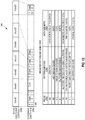
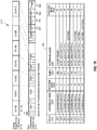
- Examples of fixed patterns that can be used with the frequent pattern compression data compression mechanism 312 in Figure 16 is shown in table 332 in Figure 17 , where the fixed patterns are provided in a pattern column 334, with its length in a length column 336 and the definition of the pattern in a pattern definition column 338.
- the flags definitions are shown in a flag definition table 340 to allow the CMC 36 to correlate a given pattern linked to a prefix code to a definition used to create uncompressed data.
- the flag definition table 340 includes the bits for a given flag in a flags column 342, the value of the bits for a given flag in a flag value column 344, and a flag definition for a given flag in a flag definition column 346.
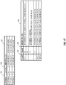
- Figure 18 illustrates another example of 64-bit frequent pattern compression data compression mechanism 348.
- the source data in a source data format 350 to be compressed is shown by example as 128 bytes.
- a new compressed data format 352 is provided in a different format of prefix codes Px, data Datax, flags, and patterns, which are organized to be grouped together for efficiency purposes.
- the prefix code is 4-bits.
- the prefix codes are shown in prefix code columns 354, 356 in a frequency pattern encoding table 358 that shows the pattern encoded in pattern encoded columns 360, 362 for a given prefix code in the prefix code columns 354, 356.
- the data size for the pattern encoded is provided in data size columns 364, 366 of the frequency pattern encoding table 358.
- the prefix code 0000 signifies an all zero data block, which can be provided as 0 bits in the data of the new compressed data format 352.
- the prefix code 1111 signifies a data block that is not compressed in the new compressed data format 352.
- Other patterns are shown in the frequency pattern encoding table 358 for prefix codes 0001-1110, which can include combinations of defined patterns as shown therein.
- the flags field in the new compressed data format 352 indicates which patterns for prefix codes 0000-1110 are present in the data portions (i.e., Datax) of the compressed data. If the pattern is present in the compressed data, the patterns are stored in the new compressed data format 352 that can then be consulted to recreate the uncompressed data.
- the new compressed data format 352 is shown as only containing patterns 0-5, because these were the only patterns accounted for in the prefix codes 0000-1110 present in the source data in this example.
- the data fields include the compressed data according to the prefix code associated with the data field in the new compressed data format 352.
- Providing memory bandwidth compression using CMCs in a CPU-based system may be provided in or integrated into any processor-based device.
- Examples include a set top box, an entertainment unit, a navigation device, a communications device, a fixed location data unit, a mobile location data unit, a mobile phone, a cellular phone, a computer, a portable computer, a desktop computer, a personal digital assistant (PDA), a monitor, a computer monitor, a television, a tuner, a radio, a satellite radio, a music player, a digital music player, a portable music player, a digital video player, a video player, a digital video disc (DVD) player, and a portable digital video player.
- PDA personal digital assistant
- Figure 19 illustrates an example of a processor-based system 368 that can employ the SoC 10' of Figure 2 with the CMC 36 of Figure 2 .
- the processor-based system 368 includes one or more CPUs 370, each including one or more processors 372.
- the CPU(s) 370 may have cache memory 374 coupled to the processor(s) 372 for rapid access to temporarily stored data.
- the CPU(s) 370 is coupled to a system bus 376 and can intercouple devices included in the processor-based system 368.
- the CPU(s) 370 communicates with these other devices by exchanging address, control, and data information over the system bus 376.
- the CPU(s) 370 can communicate bus transaction requests to a memory controller 378 as an example of a slave device.
- multiple system buses 376 could be provided.
- Other devices can be connected to the system bus 376. As illustrated in Figure 19 , these devices can include a memory system 380, one or more input devices 382, one or more output devices 384, one or more network interface devices 386, and one or more display controllers 388, as examples.
- the input device(s) 382 can include any type of input device, including but not limited to input keys, switches, voice processors, etc.
- the output device(s) 384 can include any type of output device, including but not limited to audio, video, other visual indicators, etc.
- the network interface device(s) 386 can be any devices configured to allow exchange of data to and from a network 390.
- the network 390 can be any type of network, including but not limited to a wired or wireless network, a private or public network, a local area network (LAN), a wide local area network, wireless local area network, BLUETOOTH (BT), and the Internet.
- the network interface device(s) 386 can be configured to support any type of communications protocol desired.
- the memory system 380 can include one or more memory units 392(0)-392(N).
- the CPU(s) 370 may also be configured to access the display controller(s) 388 over the system bus 376 to control information sent to one or more displays 394.
- the display controller(s) 388 sends information to the display(s) 394 to be displayed via one or more video processors 396, which process the information to be displayed into a format suitable for the display(s) 394.
- the display(s) 394 can include any type of display, including but not limited to a cathode ray tube (CRT), a liquid crystal display (LCD), a light emitting diode (LED) display, a plasma display, etc.
- DSP Digital Signal Processor
- ASIC Application Specific Integrated Circuit
- FPGA Field Programmable Gate Array
- a processor may be a microprocessor, but in the alternative, the processor may be any conventional processor, controller, microcontroller, or state machine.
- a processor may also be implemented as a combination of computing devices, e.g., a combination of a DSP and a microprocessor, a plurality of microprocessors, one or more microprocessors in conjunction with a DSP core, or any other such configuration.
- RAM Random Access Memory
- ROM Read Only Memory
- EPROM Electrically Programmable ROM
- EEPROM Electrically Erasable Programmable ROM
- registers a hard disk, a removable disk, a CD-ROM, or any other form of computer readable medium known in the art.
- An exemplary storage medium is coupled to the processor such that the processor can read information from, and write information to, the storage medium.
- the storage medium may be integral to the processor.
- the processor and the storage medium may reside in an ASIC.
- the ASIC may reside in a remote station.
- the processor and the storage medium may reside as discrete components in a remote station, base station, or server.
- data, instructions, commands, information, signals, bits, symbols, and chips that may be referenced throughout the above description may be represented by voltages, currents, electromagnetic waves, magnetic fields or particles, optical fields or particles, or any combination thereof.
- the previous description of the disclosure is provided to enable any person skilled in the art to make or use the disclosure.
- Various modifications to the disclosure will be readily apparent to those skilled in the art, and the generic principles defined herein may be applied to other variations without departing from the scope of the disclosure.
- the disclosure is not intended to be limited to the examples and designs described herein, but is to be accorded the widest scope consistent with the principles and novel features disclosed herein.
Description
- The technology of the disclosure relates generally to computer memory systems, and particularly to memory controllers in computer memory systems for providing central processing units (CPUs) with a memory access interface to memory.
- Microprocessors perform computational tasks in a wide variety of applications. A typical microprocessor application includes one or more central processing units (CPUs) that execute software instructions. The software instructions may instruct a CPU to fetch data from a location in memory, perform one or more CPU operations using the fetched data, and generate a result. The result may then be stored in memory. As non-limiting examples, this memory can be a cache local to the CPU, a shared local cache among CPUs in a CPU block, a shared cache among multiple CPU blocks, or main memory of the microprocessor.
- In this regard,
Figure 1 is a schematic diagram of an exemplary system-on-a-chip (SoC) 10 that includes a CPU-basedsystem 12. The CPU-basedsystem 12 includes a plurality of CPU blocks 14(1)-14(N) in this example, wherein 'N' is equal to any number of CPU blocks 14(1)-14(N) desired. In the example ofFigure 1 , each of the CPU blocks 14(1)-14(N) contains two CPUs 16(1), 16(2). The CPU blocks 14(1)-14(N) further contain shared Level 2 (L2) caches 18(1)-18(N), respectively. A shared Level 3 (L3)cache 20 is also provided for storing cached data that is used by any of, or shared among, each of the CPU blocks 14(1)-14(N). Aninternal system bus 22 is provided to enable each of the CPU blocks 14(1)-14(N) to access the sharedL3 cache 20 as well as other shared resources. Other shared resources accessed by the CPU blocks 14(1)-14(N) through theinternal system bus 22 may include amemory controller 24 for accessing a main, external memory (e.g., double-rate dynamic random access memory (DRAM) (DDR), as a non-limiting example),peripherals 26,other storage 28, an express peripheral component interconnect (PCI) (PCI-e)interface 30, a direct memory access (DMA)controller 32, and/or an integrated memory controller (IMC) 34. -
US 2012/317334 discloses such a controller for compressing/decompressing data to be written/read form a memory. - As CPU-based applications executing in the CPU-based
system 12 inFigure 1 increase in complexity and performance, the memory capacity requirements of the shared L2 cache 18(1)-18(N) and the sharedL3 cache 20, and external memory accessible through thememory controller 24 may also increase. Data compression may be employed to increase the effective memory capacity of the CPU-basedsystem 12 without increasing physical memory capacity. However, the use of data compression may increase memory access latency and consume additional memory bandwidth, as multiple memory access requests may be required to retrieve data, depending on whether the data is compressed or uncompressed. Accordingly, it is desirable to increase memory capacity of the CPU-basedsystem 12 using data compression while mitigating the impact on memory access latency and memory bandwidth. - The invention relates to methods and apparatuses as specified by claims 1-14.
- In another aspect, a CMC is provided. The CMC comprises a memory interface configured to access a system memory via a system bus. The CMC is configured to receive a memory read request comprising a physical address of a memory block to be accessed within a memory line in the system memory. The CMC is further configured to read a master directory memory block containing a CI corresponding to the physical address from a master directory in the system memory. The CMC is also configured to determine, based on the CI, a number of memory blocks within the memory line in the system memory to read for the memory read request. The CMC is additionally configured to read the determined number of memory blocks within the memory line in the system memory beginning at the physical address.
- In another aspect, a CMC is provided. The CMC comprises a memory interface configured to access a system memory via a system bus. The CMC is configured to receive a memory write request comprising write data and a physical address of a memory block to be written within a memory line in the system memory. The CMC is further configured to determine a compression pattern for the write data. The CMC is also configured to generate a CI for the write data based on the compression pattern. The CMC is additionally configured to update a stored CI corresponding to the physical address in a master directory with the generated CI. The CMC is further configured to write the write data to one or more memory blocks in the memory line in the system memory based on the generated CI. The CMC is also configured to write the generated CI into one or more ECC bits of each of the one or more memory blocks in the memory line of the system memory.
- In another aspect, a method for providing memory bandwidth compression for memory read requests is provided. The method comprises receiving, by a CMC via a system bus, a memory read request comprising a physical address of a memory block to be accessed within a memory line in a system memory. The method further comprises reading a master directory memory block containing a CI corresponding to the physical address from a master directory in the system memory. The method also comprises determining, based on the CI, a number of memory blocks within the memory line in the system memory to read for the memory read request. The method additionally comprises reading the determined number of memory blocks within the memory line in the system memory beginning at the physical address.
- In another aspect, a method for providing memory bandwidth compression for memory write requests is provided. The method comprises receiving, by a CMC via a system bus, a memory write request comprising write data and a physical address of a memory block to be written within a memory line in a system memory. The method further comprises determining a compression pattern for the write data. The method also comprises generating a CI for the write data based on the compression pattern. The method additionally comprises updating a stored CI corresponding to the physical address in a master directory with the generated CI. The method further comprises writing the write data to one or more memory blocks in the memory line in the system memory based on the generated CI. The method also comprises writing the generated CI into one or more ECC bits of each of the one or more memory blocks in the memory line of the system memory.
- In other aspects, compression methods and formats that may be well-suited for small data block compression are disclosed. These compression methods and formats can be employed for memory bandwidth compression aspects disclosed herein.
- With some or all aspects of these CMCs and compression mechanisms, it may be possible to decrease memory access latency and effectively increase memory bandwidth of a CPU-based system, while mitigating an increase in physical memory size and minimizing the impact on system performance.
-
-
Figure 1 is a schematic diagram of an exemplary system-on-a-chip (SoC) that includes a central processing unit (CPU)-based system; -
Figure 2 is a schematic diagram of an SoC that includes an exemplary CPU-based system having a plurality of CPUs and a compressed memory controller (CMC) configured to provide memory bandwidth compression; -
Figure 3 is a more detailed schematic diagram of the CMC ofFigure 2 , wherein the CMC is further communicatively coupled to an optional, internal memory that may be employed to provide memory bandwidth compression; -
Figure 4 is a schematic diagram of an exemplary memory bandwidth compression mechanism that may be implemented by the CMC ofFigure 3 ; -
Figure 5 illustrates an example of the SoC ofFigure 1 that includes an optional Level 4 (L4) cache to compensate for performance loss due to address translation in the CMC; -
Figures 6A and6B are diagrams illustrating exemplary communications flows during memory read operations and memory write operations, respectively, and exemplary elements of a system memory and a master directory ofFigure 4 that may be accessed by the CMC ofFigure 3 for providing memory bandwidth compression; -
Figure 7 is a flowchart illustrating exemplary operations for performing a memory read operation by the CMC ofFigure 6A using memory bandwidth compression; -
Figure 8 is a flowchart illustrating exemplary operations for performing a memory write operation by the CMC ofFigure 6B using memory bandwidth compression; -
Figures 9A and9B are diagrams illustrating exemplary communications flows during memory read operations and memory write operations, respectively, and exemplary elements of a compression indicator (CI) cache provided by some aspects of the CMC inFigure 3 for providing memory bandwidth compression; -
Figures 10A-10C are flowcharts illustrating exemplary operations for performing a memory read operation by the CMC ofFigure 9A using the CI cache; -
Figures 11A-11C are flowcharts illustrating exemplary operations for performing a memory write operation by the CMC ofFigure 9B using the CI cache; -
Figures 12-18 illustrate exemplary data block compression formats and mechanisms, any of which may be used by the CMC ofFigure 3 to compress and decompress memory data blocks; and -
Figure 19 is a block diagram of an exemplary computing device that may include the SoC ofFigure 1 that employs the CMC ofFigure 2 . - With reference now to the drawing figures, several exemplary aspects of the present disclosure are described. The word "exemplary" is used herein to mean "serving as an example, instance, or illustration." Any aspect described herein as "exemplary" is not necessarily to be construed as preferred or advantageous over other aspects.
- Aspects disclosed herein include providing memory bandwidth compression using compressed memory controllers (CMCs) in a central processing unit (CPU)-based system. In this regard, in some aspects, a CMC is configured to provide memory bandwidth compression for memory read requests and/or memory write requests. According to some aspects, upon receiving a memory read request to a physical address in a system memory, the CMC may read a compression indicator (CI) for the physical address from a master directory and/or from error correcting code (ECC) bits associated with the physical address in the system memory. The CI in some aspects may provide the CMC with a compression pattern (e.g., indicating whether data is compressed or uncompressed and/or indicating a number of memory blocks in which compressed data is stored at the physical address). Based on the CI, the CMC determines a number of memory blocks to be read for the memory read request, and reads the determined number of memory blocks beginning at the physical address. In some aspects, upon receiving a memory write request to a physical address in the system memory, the CMC may determine a compression pattern for write data to be written, and may generate a CI for the write data based on the compression pattern. The CMC may then update the master directory and/or the ECC bits associated with the physical address, and write the write data to the system memory based on the generated CI. Some aspects of the CMC may further provide a CI cache for caching previously read CIs. In this manner, the CMC may read and write compressed and uncompressed data more efficiently, resulting in decreased memory access latency and improved system performance.
- In this regard,
Figure 2 is a schematic diagram of an SoC 10' that includes an exemplary CPU-based system 12' having a plurality of CPU blocks 14(1)-14(N) similar to the CPU-basedsystem 12 inFigure 1 . The CPU-based system 12' inFigure 2 includes some common components with the CPU-basedsystem 12 inFigure 1 , which are noted by common element numbers betweenFigures 1 and2 . For the sake of brevity, these elements will not be re-described. However, in the CPU-based system 12' inFigure 2 , aCMC 36 is provided. TheCMC 36 controls access to asystem memory 38. Thesystem memory 38 may comprise one or more double data rate (DDR) dynamic random access memories (DRAMs) 40(1)-40(R) (referred to hereinafter as "DRAM 40(1)-40(R)"), as a non-limiting example. TheCMC 36 in this example employs memory bandwidth compression according to the aspects disclosed herein and below. Similar to thememory controller 24 of the CPU-basedsystem 12 ofFigure 1 , theCMC 36 in the CPU-based system 12' inFigure 2 is shared by the CPU blocks 14(1)-14(N) through theinternal system bus 22. - To illustrate a more detailed schematic diagram of exemplary internal components of the
CMC 36 inFigure 2 ,Figure 3 is provided. In this example, theCMC 36 is provided on a separate semiconductor die 44 from semiconductor dies 46(1), 46(2) that contain the CPU blocks 14(1)-14(N) inFigure 2 . Alternatively, in some aspects theCMC 36 may be included in a common semiconductor die (not shown) with the CPU blocks 14(1)-14(N). Regardless of the die configurations, theCMC 36 is provided such that the CPU blocks 14(1)-14(N) may make memory access requests via theinternal system bus 22 to theCMC 36, and receive data from memory through theCMC 36. - With continuing reference to
Figure 3 , theCMC 36 controls operations for memory accesses to thesystem memory 38, which is shown inFigures 2 and3 as comprising DRAM 40(1)-40(R). TheCMC 36 includes a plurality of memory interfaces (MEM I/Fs) 48(1)-48(P) (e.g., DDR DRAM interfaces) used to service memory access requests (not shown). In this regard, theCMC 36 in this example includes acompression controller 50. Thecompression controller 50 controls compressing data stored to thesystem memory 38 and decompressing data retrieved from thesystem memory 38 in response to memory access requests from the CPU blocks 14(1)-14(N) inFigure 2 . In this manner, the CPU blocks 14(1)-14(N) can be provided with a virtual memory address space greater than the actual capacity of memory accessed by theCMC 36. Thecompression controller 50 can also be configured to perform bandwidth compression of information provided over theinternal system bus 22 to the CPU blocks 14(1)-14(N). - As will be discussed in more detail below, the
compression controller 50 can perform any number of compression techniques and algorithms to provide memory bandwidth compression. Alocal memory 52 is provided for data structures and other information needed by thecompression controller 50 to perform such compression techniques and algorithms. In this regard, thelocal memory 52 is provided in the form of a static random access memory (SRAM) 54. Thelocal memory 52 is of sufficient size to be used for data structures and other data storage that may be needed for thecompression controller 50 to perform compression techniques and algorithms. Thelocal memory 52 may also be partitioned to contain a cache, such as a Level 4 (L4) cache, to provide additional cache memory for internal use within theCMC 36. Thus, anL4 controller 55 may also be provided in theCMC 36 to provide access to the L4 cache. Enhanced compression techniques and algorithms may require a larger internal memory, as will be discussed in more detail below. For example, thelocal memory 52 may provide 128 kilobytes (kB) of memory. - Further, as shown in
Figure 3 and as will be described in more detail below, an optional additionalinternal memory 56 can also be provided for theCMC 36. The additionalinternal memory 56 may be provided as DRAM, as an example. As will be discussed in more detail below, the additionalinternal memory 56 can facilitate additional or greater amounts of storage of data structures and other data than in thelocal memory 52 for theCMC 36 providing memory compression and decompression mechanisms to increase the memory bandwidth compression of the CPU-based system 12'. Aninternal memory controller 58 is provided in theCMC 36 to control memory accesses to the additionalinternal memory 56 for use in compression. Theinternal memory controller 58 is not accessible or viewable to the CPU blocks 14(1)-14(N). - As noted above, the
CMC 36 inFigure 3 may perform memory bandwidth compression, including, in some aspects, zero-line compression. Thelocal memory 52 can be used to store larger data structures used for such compression. As discussed in greater detail below, memory bandwidth compression may reduce memory access latency and allow more CPUs 16(1), 16(2) or their respective threads to access a same number of memory channels while minimizing the impact to memory access latency. In some aspects, the number of memory channels may be reduced while achieving similar latency results compared to a greater number of memory channels if such compression was not performed by theCMC 36, which may result in reduced system level power consumption. - Each of the resources provided for memory bandwidth compression in the
CMC 36 inFigure 3 , including thelocal memory 52 and the additionalinternal memory 56, can be used individually or in conjunction with each other to achieve the desired balance among resources and area, power consumption, increased memory capacity through memory capacity compression, and increased performance through memory bandwidth compression. Memory bandwidth compression can be enabled or disabled, as desired. Further, the resources described above for use by theCMC 36 can be enabled or disabled to achieve the desired tradeoffs among memory capacity and/or bandwidth compression efficiency, power consumption, and performance. Exemplary memory bandwidth compression techniques using these resources available to theCMC 36 will now be discussed. - In this regard,
Figure 4 is a schematic diagram of an exemplary memorybandwidth compression mechanism 60 that can be implemented by theCMC 36 ofFigure 3 to provide memory bandwidth compression. In the memorybandwidth compression mechanism 60, thesystem memory 38 comprises a plurality ofmemory lines 62, each of which is associated with a physical address. Each of the plurality ofmemory lines 62 may be accessed by theCMC 36 using a physical address of a memory read or write request (not shown). Data (not shown) may be stored within each of thememory lines 62 in thesystem memory 38 in either compressed or uncompressed form. In some aspects, one or more ECC bits comprising aCI 64 may be stored in association with eachmemory line 62 to indicate whether thememory line 62 is stored in compressed form or not. In this manner, when performing a memory access request to thesystem memory 38, theCMC 36 can check theCI 64 associated with thememory line 62 corresponding to the physical address to be addressed to determine if thememory line 62 is compressed as part of processing of the memory access request. - A
master directory 66 is also provided in thesystem memory 38. Themaster directory 66 contains oneentry 68 permemory line 62 in thesystem memory 38 corresponding to the physical address. Themaster directory 66 also contains one (1)CI 64 perentry 68 to denote if thememory line 62 is stored as compressed in thememory line 62, and if so, a compression pattern indicating a compression length of data, in aspects in which multiple compression lengths are supported. For example, if thememory line 62 is 128 bytes in length and the data stored therein can be compressed to 64 bytes or less, theCI 64 in themaster directory 66 corresponding to the data stored in thesystem memory 38 may be set to indicate that the data is stored in the first 64 bytes of the 128byte memory line 62. - With continuing reference to
Figure 4 , during a write operation, theCMC 36 can compress a memory block to be written into thesystem memory 38. For example, data (e.g., 128 bytes, or 256 bytes) is compressed. If the compressed data block is smaller than or equal to the memory block size of the system memory 38 (e.g., 64 bytes), then 64 bytes can be written, otherwise 128 bytes are written. 256 bytes could be written as 64, 128, 192, or 256 bytes, depending on the compressed data size. TheCI 64 stored in one or more ECC bits associated with thememory line 62 in thesystem memory 38 can also be set to denote if the data at thememory line 62 is compressed or not. - During a read operation example, the
CMC 36 can read theCI 64 from themaster directory 66 to determine whether the data to be read was compressed in thesystem memory 38. Based on theCI 64, theCMC 36 can read the data to be accessed from thesystem memory 38. If the data to be read was compressed in thesystem memory 38 as indicated by theCI 64, theCMC 36 can read the entire compressed data block with one memory read operation. If the portion of data read was not compressed in thesystem memory 38, memory access latency may be negatively impacted because the additional portions of thememory line 62 to be read must also be read from thesystem memory 38. In some aspects, a training mechanism may be employed, for a number of address ranges, in which theCMC 36 may be configured to "learn" whether it is better to read the data in two accesses from thesystem memory 38 in a given set of circumstances, or whether it is better to read the full amount of data from thesystem memory 38 to avoid the latency impact. - In the example of
Figure 4 , aCI cache 70 may also be provided in a separate cache outside of thesystem memory 38. TheCI cache 70 provides onecache entry 72 permemory line 62 in thesystem memory 38 to denote if amemory line 62 in thesystem memory 38 is stored in compressed form or not. In this manner, when performing a memory access request to thesystem memory 38, theCMC 36 can first check thecache entry 72 in theCI cache 70 corresponding to the physical address to be addressed to determine if thememory line 62 at the physical address in thesystem memory 38 is compressed as part of processing of the memory access request without having to read thememory line 62. Thus, if theCI cache 70 indicates that thememory line 62 is stored compressed, theCMC 36 does not have to read out theentire memory line 62, thus reducing latency. If theCI cache 70 indicates that thememory line 62 is stored uncompressed, theCMC 36 can read out theentire memory line 62. If a miss occurs in theCI cache 70, the correspondingCI 64 stored in themaster directory 66 can be consulted and loaded into theCI cache 70 for subsequent memory access requests to the same physical address. - In some aspects, the
CI cache 70 may be organized as a conventional cache. TheCI cache 70 may contain a tag array and may be organized as an n-way associative cache, as a non-limiting example. TheCMC 36 may implement an eviction policy with respect to theCI cache 70. In theCI cache 70 shown inFigure 4 , eachcache line 74 may storemultiple cache entries 72. Eachcache entry 72 may contain aCI 76 to indicate if thememory line 62 in thesystem memory 38 associated with thecache entry 72 is compressed, and/or to represent a compression pattern indicating compression size for the data corresponding to thecache entry 72. For example, theCI 76 may comprise two (2) bits representing four (4) potential compression sizes (e.g., 32, 64, 96, or 128 bytes). Note that in this example, theCI 64 is redundant, because this information is also stored in theCI 76 in thecache entries 72. For example, if thememory line 62 is 128 bytes in length and the data stored therein can be compressed to 64 bytes or less, theCI 76 in thecache entry 72 in theCI cache 70 corresponding to thememory line 62 in thesystem memory 38 may be set to indicate that the data is stored in the first 64 bytes of a 128byte memory line 62. - It may also be desired to provide an additional cache for memory bandwidth compression mechanism. In this regard,
Figure 5 illustrates an example of analternative SoC 10" like the SoC 10' inFigure 2 , but theSoC 10" inFigure 5 additionally includes anoptional cache 78, which is an L4 cache in this example. TheCMC 36 can look up a physical address in both theL4 cache 78 and theCI cache 70 concurrently to minimize latency. The addresses in theL4 cache 78 are physical addresses that are uncompressed. Upon a physical address hit in theL4 cache 78, the physical address lookup in theCI cache 70 is redundant. Upon a physical address miss in theL4 cache 78, a physical address lookup in theCI cache 70 is required to obtain the data from thesystem memory 38. Also, to avoid additional latency of aCPU 16 accessing both theL4 cache 78 and theCI cache 70, theL4 cache 78 and theCI cache 70 may be primed. -
Figures 6A and6B are provided to illustrate exemplary communications flows and exemplary elements of thesystem memory 38 and themaster directory 66 ofFigure 4 that may be accessed by theCMC 36 ofFigure 3 for providing memory bandwidth compression. In particular,Figure 6A illustrates exemplary communications flows during a memory read operation, whileFigure 6B illustrates exemplary communications flows during a memory write operation, respectively. In describingFigures 6A and6B , elements ofFigures 3 and4 are referenced for the sake of clarity. - In
Figures 6A and6B , thesystem memory 38 includes a plurality of memory lines 80(0)-80(X) for storing compressed and uncompressed data. The memory lines 80(0)-80(X) are each subdivided into respective memory blocks 82(0)-82(Z) and 84(0)-84(Z), as determined by an underlying memory architecture of thesystem memory 38. In some aspects, the size of each of the memory blocks 82(0)-82(Z), 84(0)-84(Z) represents a smallest amount of data that may be read from thesystem memory 38 in a memory read operation. For example, in some exemplary memory architectures, each of the memory lines 80(0)-80(X) may comprise 128 bytes of data, subdivided into two 64-byte memory blocks 82(0)-82(Z), 84(0)-84(Z). Some aspects may provide that each of the memory lines 80(0)-80(X) may comprise more or fewer bytes of data (e.g., 256 bytes or 64 bytes, as non-limiting examples). Similarly, according to some aspects, the memory blocks 82(0)-82(Z), 84(0)-84(Z) within the memory lines 80(0)-80(X) may be larger or smaller (e.g., 128 bytes or 32 bytes, as non-limiting examples). In some aspects, a memory read operation may read fewer bytes than the size of each of the memory blocks 82(0)-82(Z), 84(0)-84(Z), but still consume the same amount of memory bandwidth as one of the memory blocks 82(0)-82(Z), 84(0)-84(Z). - Each of the memory blocks 82(0)-82(Z), 84(0)-84(Z) is associated with one or more corresponding ECC bits 86(0)-86(Z), 88(0)-88(Z). ECC bits such as the ECC bits 86(0)-86(Z), 88(0)-88(Z) are used conventionally to detect and correct commonly encountered types of internal data corruption within the memory blocks 82(0)-82(Z), 84(0)-84(Z). In the example of
Figures 6A and6B , one or more of the ECC bits 86(0)-86(Z), 88(0)-88(Z) are repurposed to store CIs 90(0)-90(Z), 92(0)-92(Z) for the respective memory blocks 82(0)-82(Z), 84(0)-84(Z). Although the ECC bits 86(0)-86(Z), 88(0)-88(Z) inFigures 6A and6B are depicted as being adjacent to their respective memory blocks 82(0)-82(Z), 84(0)-84(Z), it is to be understood that the ECC bits 86(0)-86(Z), 88(0)-88(Z) may be located elsewhere within thesystem memory 38. - In the example of
Figures 6A and6B , thesystem memory 38 also includes themaster directory 66, which includes multiple master directory memory blocks 94(0)-94(Y). Each of the master directory memory blocks 94(0)-94(Y) is the same size as the memory blocks 82(0)-82(Z), 84(0)-84(Z). The master directory memory blocks 94(0)-94(Y) store CIs 96(0)-96(W), 98(0)-98(W), 100(0)-100(W), each of which corresponds to a physical address of one of the memory blocks 82(0)-82(Z), 84(0)-84(Z). As discussed in greater detail below, in some aspects, the CIs 90(0)-90(Z), 92(0)-92(Z) stored in the ECC bits 86(0)-86(Z), 88(0)-88(Z) and the CIs 96(0)-96(W), 98(0)-98(W), 100(0)-100(W) stored in the master directory memory blocks 94(0)-94(Y) may be maintained so as to always store the same value for a given one of the memory blocks 82(0)-82(Z), 84(0)-84(Z). Some aspects may provide that the CIs 90(0)-90(Z), 92(0)-92(Z) stored in the ECC bits 86(0)-86(Z), 88(0)-88(Z) may be updated more frequently than the CIs 96(0)-96(W), 98(0)-98(W), 100(0)-100(W) in the master directory memory blocks 94(0)-94(Y). - The CIs 90(0)-90(Z), 92(0)-92(Z) and the CIs 96(0)-96(W), 98(0)-98(W), 100(0)-100(W) each may comprise one or more bits that indicate a compression status of data stored at a corresponding memory block 82(0)-82(Z), 84(0)-84(Z) of the
system memory 38. In some aspects, each of the CIs 90(0)-90(Z), 92(0)-92(Z) and the CIs 96(0)-96(W), 98(0)-98(W), 100(0)-100(W) may comprise a single bit indicating whether data in the corresponding memory block 82(0)-82(Z), 84(0)-84(Z) is compressed or uncompressed. According to some aspects, each of the CIs 90(0)-90(Z), 92(0)-92(Z) and the CIs 96(0)-96(W), 98(0)-98(W), 100(0)-100(W) may comprise multiple bits that may be used to indicate a compression pattern (e.g., a number of the memory blocks 82(0)-82(Z), 84(0)-84(Z) occupied by the compressed data, as a non-limiting example) for each of the corresponding memory blocks 82(0)-82(Z), 84(0)-84(Z). - In the example of
Figure 6A , a memory readrequest 102 specifying aphysical address 104 is received by theCMC 36, as indicated byarrow 106. For purposes of illustration, it is assumed in this example that thephysical address 104 corresponds to the memory block 82(0), which is a 64-byte subdivision of the 128-byte memory line 80(0). At the time the memory readrequest 102 is received, theCMC 36 is unaware of whether the data stored at the memory block 82(0) is compressed or not. TheCMC 36 could proceed with reading the entire memory line 80(0), but if the requested data is stored in compressed form in only the memory block 82(0), a read of the memory block 82(Z) would be unnecessary, and would result in increased memory access latency. Alternatively, theCMC 36 could read only memory block 82(0), determine based on its contents whether the data stored therein is compressed or not, and then read the memory block 82(Z) if the data is uncompressed. However, this approach may also result in increased memory access latency resulting from issuing the two separate memory read operations. Thus, without knowing the compression status of the memory block 82(0), theCMC 36 risks executing unnecessary memory read operations that may negatively impact memory access latency. - By using the CIs 90(0)-90(Z), 92(0)-92(Z) and/or the CIs 96(0)-96(W), 98(0)-98(W), 100(0)-100(W), the
CMC 36 may determine how many memory blocks 82(0)-82(Z) should be read to ensure that all data (compressed or uncompressed) for a given memory readrequest 102 is efficiently read from thesystem memory 38. Thus, after receiving the memory readrequest 102, theCMC 36 may read the master directory memory block 94(0) of themaster directory 66 to access the CI 96(0) corresponding to thephysical address 104 of the memory block 82(0), as indicated byarrow 108. The CI 96(0) may then be used by theCMC 36 to determine how many memory blocks 82(0)-82(Z) within the memory line 80(0) to read to ensure that the data requested by the memory readrequest 102 is efficiently retrieved. - In some aspects, the
CMC 36 may determine how many memory blocks 82(0)-82(X) to read by determining a compression pattern (not shown) indicated by the CI 96(0). In the example above, the CI 96(0) may be a single bit indicating that data is compressed (i.e., only the memory block 82(0) should be read) or uncompressed (i.e., both the memory blocks 82(0) and 82(Z) should be read). According to aspects in which the memory lines 80(0)-80(X) of thesystem memory 38 each contain more than two memory blocks 82(0)-82(Z), 84(0)-84(Z), the CI 96(0) may comprise multiple bits indicating how many memory blocks 82(0)-82(Z) contain compressed data. For example, if the memory lines 80(0)-80(X) were 256-byte memory lines subdivided into four 64-byte memory blocks 82(0)-82(Z), the CI 96(0) may indicate that compressed data is stored in 64 bytes, 128 bytes, or 192 bytes (corresponding to the memory block 82(0), the memory blocks 82(0)-82(1), and the memory blocks 82(0)-82(2), respectively). Based on the CI 96(0), theCMC 36 may then issue an appropriate number of memory read operations to read the determined number of memory blocks 82(0)-82(Z) within the memory line 80(0), as indicated byarrow 110. Some aspects may provide that theCMC 36 may determine that the compression pattern indicated by the CI 96(0) comprises a zero-line indicator, which indicates to theCMC 36 that data stored at thephysical address 104 is made up entirely of zero values. In such case, theCMC 36 may read zero memory blocks 82(0)-82(Z). According to some aspects, theCMC 36 may determine that the compression pattern indicated by the CI 96(0) comprises an indicator of other fixed data patterns stored at the physical address 104 (such as all ones (Is), as a non-limiting example). - In some aspects, it may be desirable to read the CIs 96(0)-96(W), 98(0)-98(W), 100(0)-100(W) from the
master directory 66 for only a certain percentage of memory readrequests 102 received by theCMC 36. For example, in some aspects, themaster directory 66 may only be accessed for ten percent (10%) of memory readrequests 102 received by theCMC 36. In such aspects, upon receiving the memory readrequest 102, theCMC 36 may probabilistically determine (e.g., based on a random number generator (not shown)) whether to read the CI 96(0) for the memory block 82(0) from themaster directory 66, or alternatively whether to read the CI 90(0) for the memory block 82(0) from the ECC bits 86(0). In the latter case, theCMC 36 may read the CI 90(0), as indicated by dashedarrow 112, and use the CI 90(0) in determining how many memory blocks 82(0)-82(Z) to read from the memory line 80(0). - Referring now to
Figure 6B , theCMC 36 receives amemory write request 114, as indicated byarrow 116. Thememory write request 114 includes both writedata 118 to be written to thesystem memory 38, as well as thephysical address 104 of thesystem memory 38 to which thewrite data 118 is to be written. For purposes of illustration, it is again assumed that thephysical address 104 corresponds to the memory block 82(0). Upon receiving thememory write request 114, theCMC 36 may carry out operations to compress thewrite data 118, and based on the results of compressing thewrite data 118, may determine a compression pattern for thewrite data 118. The compression pattern may indicate, as non-limiting examples, whether or not thewrite data 118 was successfully compressed, and/or a number of memory blocks 82(0)-82(Z) occupied by thecompressed write data 118. Based on the compression pattern, theCMC 36 generates aCI 120 for thewrite data 118. - The
CMC 36 may then update the CI 96(0) stored in themaster directory 66 for thephysical address 104 of the memory block 82(0) with the generatedCI 120, as indicated byarrow 122. According to some aspects, themaster directory 66 may be updated for only a certain percentage of memory write requests 114 received by theCMC 36. For example, in some aspects, themaster directory 66 may only be updated for ten percent (10%) of memory write requests 114 received by theCMC 36. Accordingly, in such aspects, theCMC 36 may probabilistically determine (e.g., based on a random number generator (not shown)) whether to update the stored CI 96(0) for the memory block 82(0) in themaster directory 66. If not, this operation may be omitted. TheCMC 36 then writes thewrite data 118 to one or more of the memory blocks 82(0)-82(Z), as indicated byarrow 124. TheCMC 36 also writes the generatedCI 120 into the CIs 90(0)-90(Z) stored in the ECC bits 86(0)-86(Z) of the one or more memory blocks 82(0)-82(Z) to which thewrite data 118 was written, as indicated byarrow 126. -
Figure 7 is a flowchart that illustrates exemplary operations for performing a memory read operation by theCMC 36 ofFigure 3 using memory bandwidth compression, as discussed with respect toFigure 6A . For the sake of clarity, elements ofFigures 2 ,3 , and6A are referenced in describingFigure 7 . InFigure 7 , operations begin with theCMC 36 receiving, via theinternal system bus 22, the memory readrequest 102 comprising thephysical address 104 of the memory block 82(0) to be accessed within the memory line 80(0) in the system memory 38 (block 128). In some aspects, theCMC 36 optionally may probabilistically determine whether the CI 96(0) should be read from the master directory 66 (block 130). If theCMC 36 determines that the CI 96(0) should not be read from themaster directory 66, theCMC 36 reads the CI 90(0) from the one or more ECC bits 86(0) along with reading the memory block 82(0), and uses the CI 90(0) as the CI 96(0) (block 132). However, if theCMC 36 is not using probabilistic determination, or if theCMC 36 probabilistically determines atdecision block 130 that the CI 96(0) should be read from themaster directory 66, theCMC 36 reads the master directory memory block 94(0) containing the CI 96(0) corresponding to thephysical address 104 from themaster directory 66 in the system memory 38 (block 134). - The
CMC 36 then determines, based on the CI 96(0), a number of memory blocks 82(0)-82(Z) within the memory line 80(0) in thesystem memory 38 to read for the memory read request 102 (block 136). In some aspects, the operations ofblock 136 for determining the number of memory blocks 82(0)-82(Z) to read may comprise determining a compression pattern indicated by the CI 96(0) (block 138). For example, theCMC 36 may determine that the CI 96(0) comprises a zero-line indicator indicating that zero memory blocks 82(0)-82(Z) should be read (block 140). TheCMC 36 then reads the determined number of memory blocks 82(0)-82(Z) within the memory line 80(0) in thesystem memory 38 beginning at the physical address 104 (block 142). - To illustrate exemplary operations for performing a memory write operation by the
CMC 36 ofFigure 3 using memory bandwidth compression, as discussed above with respect toFigure 6B ,Figure 8 is provided. In this regard, elements ofFigures 2 ,3 , and6B are referenced in describingFigure 8 for the sake of clarity. Operations inFigure 8 begin with theCMC 36 receiving, via theinternal system bus 22, thememory write request 114 comprising thewrite data 118 and thephysical address 104 of the memory block 82(0) to be written within the memory line 80(0) in the system memory 38 (block 144). After attempting to compress thewrite data 118, theCMC 36 determines a compression pattern for the write data 118 (e.g., whether thewrite data 118 was compressed, and/or how many memory blocks 82(0)-82(Z) are required to store the write data 118) (block 146). Based on the compression pattern, theCMC 36 generates aCI 120 for thewrite data 118 based on the compression pattern (block 148). - According to some aspects, the
CMC 36 optionally may probabilistically determine whether the CI 96(0) stored in themaster directory 66 should be updated (block 150). If theCMC 36 determines that the stored CI 96(0) in themaster directory 66 should not be updated, processing resumes atblock 152 ofFigure 8 . However, if theCMC 36 determines atdecision block 150 that the stored CI 96(0) in themaster directory 66 should be updated, or if theCMC 36 is not employing probabilistic determination, theCMC 36 updates the stored CI 96(0) corresponding to thephysical address 104 in themaster directory 66 with the generated CI 120 (block 154). - The
CMC 36 next writes thewrite data 118 to one or more of the memory blocks 82(0)-82(Z) in the memory line 80(0) in thesystem memory 38 based on the generated CI 120 (block 152). TheCMC 36 also writes the generatedCI 120 into one or more ECC bits 86(0)-86(Z) of each of the memory blocks 82(0)-82(Z) in the memory line 80(0) of the system memory 38 (block 156). In some aspects, the generatedCI 120 is written into the ECC bits 86(0) as part of the same memory write operation that writes thewrite data 118 to the first memory block 82(0). - As noted above with respect to
Figure 4 , memory bandwidth compression provided by theCMC 36 may be further enhanced in some aspects through the use of theCI cache 70 ofFigure 4 . In this regard,Figures 9A and9B are provided to illustrate exemplary communications flows and exemplary elements of theCI cache 70 that may be accessed by theCMC 36 ofFigure 3 for providing memory bandwidth compression. In particular,Figures 9A and9B illustrate exemplary communications flows during a memory read operation and a memory write operation, respectively, using theCI cache 70. In describingFigures 9A and9B , elements ofFigures 3 ,4 ,6A , and6B are referenced for the sake of clarity. - As seen in
Figure 9A , theCI cache 70 of theCMC 36 includes multiple CI cache entries 158(0)-158(T) storing cached CIs 160(0)-160(W), 162(0)-162(W), and 164(0)-164(W). Each of the cache entries 158(0)-158(T) is the same size as the master directory memory blocks 94(0)-94(Y), and in some aspects are configured to store one of the master directory memory blocks 94(0)-94(Y) that is read in the course of a memory read operation or a memory write operation by theCMC 36. In this manner, theCMC 36 may access the cached CIs 160(0)-160(W), 162(0)-162(W), and 164(0)-164(W) on subsequent memory read operations and memory write operations, rather than having to access thesystem memory 38 to read the CIs 90(0)-90(Z), 92(0)-92(Z) and/or the CIs 96(0)-96(W), 98(0)-98(W), 100(0)-100(W). Because theCMC 36 may read from and write to theCI cache 70 much faster than reading from and writing to thesystem memory 38, the use of theCI cache 70 may enable theCMC 36 to further decrease memory access latency. - In the example of
Figure 9A , theCMC 36 providing theCI cache 70 receives the memory readrequest 102 comprising thephysical address 104, as indicated byarrow 166. It is assumed that thephysical address 104 corresponds to the memory block 82(0) of the memory line 80(0) of thesystem memory 38. TheCMC 36 may then determine whether thephysical address 104 corresponds to one of the CI cache entries 158(0)-158(T). If one of the CI cache entries 158(0)-158(T), such as the CI cache entry 158(0), corresponds to thephysical address 104 of the memory block 82(0) (i.e., a cache "hit"), then theCMC 36 has identified the CI cache entry 158(0) that includes a CI indicator, such as the CI 160(0), for the memory block 82(0). TheCMC 36 then reads the CI 160(0) from the CI cache entry 158(0) of theCI cache 70, and determines a number of memory blocks 82(0)-82(Z) to read based on the CI 160(0) as discussed above with respect toFigure 6A . - However, if the
CMC 36 determines that thephysical address 104 does not correspond to any of the CI cache entries 158(0)-158(T), theCMC 36 may read the master directory memory block 94(0) of themaster directory 66 to access the CI 96(0) corresponding to thephysical address 104 of the memory block 82(0), as indicated byarrow 168. As noted above, in some aspects it may be desirable for theCMC 36 to read themaster directory 66 for only a certain percentage of memory readrequests 102 received by theCMC 36. Accordingly, in such aspects, theCMC 36 may probabilistically determine (e.g., based on a random number generator (not shown)) whether to read the master directory memory block 94(0) from themaster directory 66, or alternatively to read the CI 90(0) for the memory block 82(0) from the ECC bits 86(0). In the latter case, theCMC 36 may read the CI 90(0), as indicated by dashedarrow 170. TheCMC 36 may then use the CI 90(0) without further updating theCI cache 70. - The
CMC 36 may then write the master directory memory block 94(0) into theCI cache 70 as a new CI cache entry 158(0). In some aspects, before writing the master directory memory block 94(0) as the new CI cache entry 158(0), theCI cache 70 may first determine whether a current CI cache entry 158(0) must be evicted. If so, theCI cache 70 may further determine whether the current CI cache entry 158(0) has been modified since being written into the CI cache 70 (e.g., by determining whether at least one cached CI 160(0)-160(W) has been changed since being read from the master directory 66). In some aspects, theCI cache 70 may determine whether the current CI cache entry 158(0) has been modified by checking to see if a dirty bit (not shown) associated with the current CI cache entry 158(0) has been set. If the current CI cache entry 158(0) has been modified, theCMC 36 writes the current CI cache entry 158(0) to the corresponding one of the master directory memory blocks 94(0)-94(Y). TheCMC 36 then reads the CI 160(0) from the CI cache entry 158(0) of theCI cache 70, and determines a number of memory blocks 82(0)-82(Z) to read based on the CI 160(0) as discussed above. The determined number of memory blocks 82(0)-82(Z) are then read by theCMC 36, as indicated byarrow 172. - In some aspects, the
CMC 36 may issue an early memory readrequest 174, based on the memory readrequest 102, to thesystem memory 38 concurrently with determining whether thephysical address 104 corresponds to one of the CI cache entries 158(0)-158(T). The early memory readrequest 174 may be processed in parallel with theCMC 36 determining the number of memory blocks 82(0)-82(Z) to read based on the CI 160(0). Upon determining the number of memory blocks 82(0)-82(Z) to read, the early memory readrequest 174 may be modified based on the CI 160(0). As a non-limiting example, the early memory readrequest 174 may be modified to read the determined number of memory blocks 82(0)-82(Z). In this manner, additional memory bandwidth compression and decreased memory access latency may be provided through parallel processing of the early memory readrequest 174 and theCI cache 70 reads and/or writes. - Furthermore, according to some aspects discussed above with respect to
Figure 5 , theCMC 36 may also perform a cache read operation (not shown) to look up thephysical address 104 in theL4 cache 78 concurrently with determining whether thephysical address 104 corresponds to one of the CI cache entries 158(0)-158(T) in theCI cache 70. By doing so, theCMC 36 may further minimize memory access latency. - Referring now to
Figure 9B , theCMC 36 receives thememory write request 114, as indicated byarrow 176. Thememory write request 114 includes both thewrite data 118 to be written to thesystem memory 38, as well as thephysical address 104 of thesystem memory 38 to which thewrite data 118 is to be written. It is again assumed for purposes of illustration that thephysical address 104 corresponds to the memory block 82(0). Upon receiving thememory write request 114, theCMC 36 may carry out operations to compress thewrite data 118, and based on the results of compressing thewrite data 118, may determine a compression pattern for thewrite data 118. The compression pattern may indicate, as non-limiting examples, whether or not thewrite data 118 was successfully compressed, and/or a number of memory blocks 82(0)-82(Z) occupied by thecompressed write data 118. Based on the compression pattern, theCMC 36 generates theCI 120 for thewrite data 118. - The
CMC 36 may then determine whether thephysical address 104 corresponds to one of the CI cache entries 158(0)-158(T). If one of the CI cache entries 158(0)-158(T), such as the CI cache entry 158(0), corresponds to thephysical address 104 of the memory block 82(0) (i.e., a cache "hit"), then theCMC 36 has identified the CI cache entry 158(0) that includes a CI indicator, such as the CI 160(0), for the memory block 82(0). Accordingly, theCMC 36 updates the CI 160(0) of the CI cache entry 158(0) with the generatedCI 120, as indicated byarrow 178. TheCMC 36 next writes thewrite data 118 to one or more of the memory blocks 82(0)-82(Z) in the memory line 80(0), as indicated byarrow 180. TheCMC 36 also writes the generatedCI 120 into one or more of the ECC bits 86(0)-86(Z) of the one or more of the memory blocks 82(0)-82(Z) to which thewrite data 118 was written, as indicated byarrow 182. According to some aspects, the generatedCI 120 is written into the ECC bits 86(0) as part of the same memory write operation that writes thewrite data 118 to the first memory block 82(0). - However, if the
CMC 36 determines that thephysical address 104 does not correspond to any of the CI cache entries 158(0)-158(T) (i.e., a cache miss), theCMC 36 may update the stored CI 96(0) corresponding to thephysical address 104 in themaster directory 66 with the generatedCI 120, as indicated byarrow 184. TheCMC 36 may then write the master directory memory block 94(0) into theCI cache 70 as a new CI cache entry 158(0), as indicated byarrow 186. In some aspects, before writing the master directory memory block 94(0) as the new CI cache entry 158(0), theCI cache 70 may first determine whether a current CI cache entry 158(0) must be evicted. If so, theCI cache 70 may further determine whether the current CI cache entry 158(0) has been modified since being written into theCI cache 70. In some aspects, theCI cache 70 may determine whether the current CI cache entry 158(0) has been modified by checking to see if a dirty bit (not shown) associated with the CI cache entry 158(0) has been set. If the current CI cache entry 158(0) has been modified, theCMC 36 writes the current CI cache entry 158(0) to the corresponding one of the master directory memory blocks 94(0)-94(Y), as indicated byarrow 188, before writing the master directory memory block 94(0) into theCI cache 70 as the new CI cache entry 158(0). - In some aspects, the
master directory 66 may be updated in response to a cache miss in theCI cache 70 for only a certain percentage of memory write requests 114 received by theCMC 36. Accordingly, in such aspects, theCMC 36 may probabilistically determine (e.g., based on a random number generator (not shown)) whether to update the stored CI 96(0) for the memory block 82(0) in themaster directory 66. If not, the operations described above with respect to a cache miss are omitted (i.e., neither themaster directory 66 nor theCI cache 70 are updated, and the generatedCI 120 is stored in the ECC bits 86(0)-86(Z) of one or more of the memory blocks 82(0)-82(Z)). -
Figures 10A-10C are flowcharts illustrating exemplary operations for performing a memory read operation by theCMC 36 ofFigure 3 using theCI cache 70 ofFigures 9A and9B . In particular,Figure 10A illustrates operations for receiving the memory readrequest 102 and determining whether a search of theCI cache 70 for a CI 160(0) corresponding to thephysical address 104 of the memory readrequest 102 results in a hit or a miss.Figure 10B illustrates operations carried out as a result of a cache miss on theCI cache 70, whileFigure 10C illustrates operations carried out as a result of a cache hit on theCI cache 70. Elements ofFigures 2 ,3 , and9A are referenced in describingFigures 10A-10C for the sake of clarity. - Operations in
Figure 10A begin with theCMC 36 receiving, via theinternal system bus 22, the memory readrequest 102 comprising thephysical address 104 of a memory block 82(0) to be accessed within the memory line 80(0) in the system memory 38 (block 190). In some aspects, theCMC 36 may send the early memory readrequest 174 to thesystem memory 38 concurrently with subsequent operations (block 192). TheCMC 36, according to some aspects, may perform a cache read operation on an L4 cache, such as theL4 cache 78 ofFigure 5 , concurrently with subsequent operations (block 194). A determination is then made regarding whether the cache read operation on theL4 cache 78 resulted in a cache hit (block 195). If so, then the results of the cache read operation are returned, and the read to thesystem memory 38 is rendered moot (block 196). - The
CMC 36 next determines whether thephysical address 104 corresponds to a CI cache entry 158(0) of a plurality of CI cache entries 158(0)-158(T) of a CI cache 70 (block 197). If theCMC 36 determines atdecision block 196 that thephysical address 104 does not correspond to a CI cache entry 158(0) of the plurality of CI cache entries 158(0)-158(T) (i.e., a cache miss), processing resumes atblock 198 ofFigure 10B . If thephysical address 104 is determined to correspond to a CI cache entry 158(0) (i.e., a cache hit), processing resumes atblock 200 ofFigure 10C . - Referring now to
Figure 10B , theCMC 36 in some aspects may probabilistically determine whether the CI 96(0) should be read from themaster directory 66 in response to a cache miss (block 198). Note that in such aspects, the ECC bits 86(0)-86(Z), 88(0)-88(Z) of the one or more of the memory blocks 82(0)-82(Z), 84(0)-84(Z) will store the CIs 90(0)-90(Z), 92(0)-92(Z). The probabilistic determination may be made using a random number generator, as a non-limiting example. If it is determined atdecision block 198 that the CI 96(0) should be read from themaster directory 66, theCMC 36 reads the master directory memory block 94(0) containing the CI 96(0) corresponding to thephysical address 104 from themaster directory 66 in the system memory 38 (block 202). If theCMC 36 determines atdecision block 198 that the CI 96(0) should not be read from themaster directory 66, theCMC 36 reads the CI 90(0) from one or more ECC bits 86(0) along with reading the memory block 82(0) (block 204). Processing then resumes atblock 214 ofFigure 10C . - With continuing reference to
Figure 10B , theCMC 36 according to some aspects may next determine whether a current CI cache entry 158(0) of theCI cache 70 should be evicted (block 206). If not, processing resumes atblock 208 ofFigure 10B . If theCMC 36 determines atdecision block 206 that the current CI cache entry 158(0) should be evicted, theCMC 36 next determines whether the current CI cache entry 158(0) has been modified (block 210). This determination may be based on determining whether a dirty bit for the CI cache entry 158(0) has been set, as a non-limiting example. If the current CI cache entry 158(0) is determined atdecision block 210 to be unchanged, processing resumes atblock 208 ofFigure 10B . Otherwise, theCMC 36 writes the current CI cache entry 158(0) to the master directory 66 (block 212). The master directory memory block 94(0) is then written to the CI cache entry 158(0) of the CI cache 70 (block 208). Processing then resumes atblock 200 ofFigure 10C . - Turning now to
Figure 10C , theCMC 36 reads the CI 160(0) from the CI cache entry 158(0) of the CI cache 70 (block 200). TheCMC 36 next determines, based on the CI 160(0), a number of memory blocks 82(0)-82(Z) within the memory line 80(0) in thesystem memory 38 to read for the memory read request 102 (block 214). TheCMC 36 then reads the determined number of memory blocks 82(0)-82(Z) within the memory line 80(0) in thesystem memory 38 beginning at the physical address 104 (block 216). In aspects in which the early memory readrequest 174 was issued, the operations ofblock 216 for reading the determined number of memory blocks 82(0)-82(Z) may include modifying the early memory readrequest 174 based on the CI 160(0) (block 218). - To illustrate exemplary operations for performing a memory write operation by the
CMC 36 ofFigure 3 using theCI cache 70 ofFigure 8 ,Figures 11A-11C are provided.Figure 11A illustrates operations for receiving thememory write request 114 and determining whether a search of theCI cache 70 for a CI cache entry 158(0)-158(T) corresponding to thephysical address 104 of thememory write request 114 results in a hit or a miss.Figure 11B illustrates operations carried out as a result of a cache miss on theCI cache 70, whileFigure 11C illustrates operations carried out as a result of a cache hit on theCI cache 70. Elements ofFigures 2 ,3 , and9B are referenced in describingFigures 11A-11C for the sake of clarity. - In
Figure 11A , operations begin with theCMC 36, via theinternal system bus 22, amemory write request 114 comprisingwrite data 118 and thephysical address 104 of the memory block 82(0) to be written within the memory line 80(0) in the system memory 38 (block 220). TheCMC 36 determines a compression pattern for the write data 118 (block 222). In some aspects, the compression pattern may indicate whether thewrite data 118 is compressed or uncompressed, and/or a number of memory blocks 82(0)-82(Z) occupied by thewrite data 118. Based on the compression pattern, theCMC 36 generates aCI 120 for thewrite data 118 based on the compression pattern (block 224). - The
CMC 36 next determines whether thephysical address 104 corresponds to a CI cache entry 158(0) of a plurality of CI cache entries 158(0)-158(T) of a CI cache 70 (block 226). If thephysical address 104 is determined atdecision block 226 not to correspond to a CI cache entry 158(0) of the plurality of CI cache entries 158(0)-158(T) (i.e., a cache miss), processing resumes atblock 228 ofFigure 11B . However, if theCMC 36 determines atdecision block 226 that thephysical address 104 corresponds to a CI cache entry 158(0) (i.e., a cache hit), processing resumes atblock 230 ofFigure 11C . - Referring now to
Figure 11B , some aspects of theCMC 36 may probabilistically determine whether the CI 96(0) should be updated in the master directory 66 (block 228). If it is determined atdecision block 228 that the CI 96(0) should not be updated, processing resumes atblock 242 ofFigure 11C . However, if theCMC 36 determines atdecision block 228 to update the CI 96(0), or if theCMC 36 is not configured to use probabilistic determination, theCMC 36 updates the stored CI 96(0) corresponding to thephysical address 104 in themaster directory 66 with the generated CI 120 (block 232). - In some aspects, the
CMC 36 may next determine whether a current CI cache entry 158(0) of theCI cache 70 should be evicted (block 234). If not, processing resumes atblock 236 ofFigure 11B . If theCMC 36 determines atdecision block 234 that the current CI cache entry 158(0) should be evicted, theCMC 36 determines whether the current CI cache entry 158(0) has been modified (block 238). Determining whether the CI cache entry 158(0) has been modified may comprise determining whether a dirty bit of the CI cache entry 158(0) has been set, as a non-limiting example. If the current CI cache entry 158(0) is determined atdecision block 238 to be unchanged, processing resumes atblock 236 ofFigure 11B . However, if theCMC 36 determines atdecision block 238 that the current CI cache entry 158(0) has been modified, theCMC 36 writes the current CI cache entry 158(0) to the master directory 66 (block 240). TheCMC 36 then writes the stored CI 96(0) to the CI cache entry 158(0) of the CI cache 70 (block 236). Processing resumes atblock 242 ofFigure 11C . - In
Figure 11C , theCMC 36 updates the CI cache entry 158(0) of theCI cache 70 with the generated CI 120 (block 230). TheCMC 36 then writes thewrite data 118 to one or more memory blocks 82(0)-82(Z) in the memory line 80(0) in thesystem memory 38 based on the generated CI 120 (block 242). The generatedCI 120 is written into one or more ECC bits 86(0)-86(Z) of each of the one or more memory blocks 82(0)-82(Z) in the memory line 80(0) of the system memory 38 (block 244). In some aspects, the generatedCI 120 is written into the ECC bits 86(0) as part of the same memory write operation that writes thewrite data 118 to the first memory block 82(0). - As discussed above, it may be desired to provide compression of a memory data block 82(0)-82(Z) having a configurable fixed data pattern as a special case to optimize compression. For example, if a memory data block 82(0)-82(Z) (e.g., 128 bytes) is all 0's, then data is not read or written, but noted in a separate data structure as all 0's. A zero-bit could be provided in the
system memory 38 to denote if a memory line 80(0)-80(X) is compressed, thus adding one (1) bit per memory data block 82(0)-82(Z). TheCMC 36 could maintain a cache that remembers, for a number of 128-byte memory blocks 82(0)-82(Z) for example, if a block is all 0's. For a write operation, if a line of a memory data block 82(0)-82(Z) is all 0's, theCMC 36 does not write the line to thesystem memory 38, but theCI cache 70 is updated. For a read operation, the zero-bit in theCI cache 70 is checked for the line. If the line is in theCI cache 70, then depending on the zero-bit, either the line is read from thesystem memory 38, or all 0's is returned. If the line is not in theCI cache 70, then it is read from thesystem memory 38. If the line is zero, then theCI cache 70 can be updated. - The
CI cache 70 can be updated to evict acache line 74 according to known techniques (LRU, pseudo-LRU, etc.). If a line is evicted, all lines that have their zero-bit set need to be written to main memory. This can be organized as a write-all-zeros queue. A possible optimization would be to use two (2) bits, wherein one bit denotes if the line is all-zeros, and another bit denotes if the line is dirty (i.e., has not been written to main memory yet). A background task of theCMC 36 can inspect theCI cache 70 and queue the lines with dirty-bits in a "write-all-zeros" queue. With the memory bandwidth compression mechanisms described above, different memory compression mechanisms can be employed by theCMC 36 as desired. For example, it may be desired to employ memory compression mechanisms that are optimized for small data blocks, such as 64, 128, and 256 bytes, since the cache lines 74 described in the examples above include these sizes as examples. - In some aspects, a value of a CI comprising multiple bits may indicate a compression status and/or a fixed data pattern stored in a memory block such as one of the memory blocks 82(0)-82(Z). As a non-limiting example, for a CI of two (2) bits, a value of "00" may indicate that the corresponding memory block is uncompressed, while a value of "01" may indicate that the corresponding memory block is compressed. A value of "11" may indicate that a fixed pattern (e.g., all zeroes (0s) or all ones (Is)) is stored in the corresponding memory block. In such aspects, the
master directory 66 would always be updated rather than being updated subject to a probabilistic determination. - In this regard,
Figure 12 illustrates a frequent pattern compressiondata compression mechanism 246. In this regard, the source data in asource data format 248 to be compressed is shown by example as 128 bytes. Acompressed data format 250 is shown below. Thecompressed data format 250 is provided in a format of prefix codes Px and data behind the prefix as Datax. The prefix is 3-bits. The prefix codes are shown in aprefix code column 252 in a frequent pattern encoding table 254 that shows the pattern encoded in a pattern encoded column 256 for a given prefix code in theprefix code column 252. The data size for the pattern encoded is provided in adata size column 258 of the frequent pattern encoding table 254. -
Figure 13 illustrates a 32-bit frequent pattern compressiondata compression mechanism 260. In this regard, the source data in asource data format 262 to be compressed is shown by example as 128 bytes. Acompressed data format 264 is shown below. Thecompressed data format 264 is provided in a format of prefix Px and data immediately behind the prefix as Datax. A newcompressed data format 266 is provided in a different format of prefix codes Px, data Datax, flags, and patterns, which are organized to be grouped together for efficiency purposes. The prefix code is 3-bits. The prefix codes are shown in aprefix code column 268 in a frequency pattern encoding table 270 that shows the pattern encoded in a pattern encodedcolumn 272 for a given prefix code in theprefix code column 268. The data size for the pattern encoded is provided in adata size column 274 of the frequency pattern encoding table 270. Theprefix code 000 signifies an uncompressed pattern, which would be data of the full size of 32-bits in the newcompressed data format 266. Theprefix code 001 signifies an all zero data block, which can be provided as 0 bits in the data of the newcompressed data format 266. With a 3-bit prefix, prefix codes 010-111 can be used to encode other specific patterns that are recognized in the source data, which in this example are patterns in 0, 4, 8, 12, 16, and 24 bits respectively. -
Figure 14 illustrates an example of 32-bit frequent pattern compressiondata compression mechanism 276. In this regard, the source data in asource data format 278 to be compressed is shown by example as 128 bytes. Acompressed data format 280 is shown below. Thecompressed data format 280 is provided in a format of prefix Px and data behind the prefix as Datax. A newcompressed data format 282 is provided in a different format of prefix codes Px, data Datax, flags, and patterns, which are organized to be grouped together for efficiency purposes. The prefix code is 3-bits. The prefix codes are shown in aprefix code column 284 in a frequency pattern encoding table 286 that shows the pattern encoded in a pattern encodedcolumn 288 for a given prefix code in theprefix code column 284. The data size for the pattern encoded is provided in adata size column 290 of the frequency pattern encoding table 286. Theprefix code 000 signifies an uncompressed pattern, which would be data of the full size of 32-bits in the newcompressed data format 282. Theprefix code 001 signifies an all zero data block, which can be provided as 0 bits in the data of the newcompressed data format 282.Prefix code 010 signifies pattern 0xFFFFFFFF, which is a specific pattern and thus requires 0-bit data size in the compressed data according to the newcompressed data format 282. Other patterns are shown in the frequency pattern encoding table 286 for prefix codes 011-111. The flags field in the newcompressed data format 282 indicates which patterns for prefix codes 001-111 are present in the data portions (i.e., Datax) of the compressed data. If the pattern is present in the compressed data, the patterns are stored in the newcompressed data format 282 that can then be consulted to recreate the uncompressed data. The data fields include the compressed data according to the prefix code associated with the data field in the newcompressed data format 282. -
Figure 15 illustrates another example of 64-bit frequent pattern compressiondata compression mechanism 292. In this regard, the source data in asource data format 294 to be compressed is shown by example as 128 bytes. A newcompressed data format 296 is provided in a different format of prefix codes Px, data Datax, flags, and patterns, which are organized to be grouped together for efficiency purposes. The prefix code is 4-bits. The prefix codes are shown inprefix code columns columns prefix code columns data size columns prefix code 0000 signifies an all zero data block, which can be provided as 0 bits in the data of the newcompressed data format 296. Other patterns are shown in the frequency pattern encoding table 302 for prefix codes 0001-1111, which include ASCII patterns for frequently occurring ASCII patterns. The flags field in the newcompressed data format 296 indicates which patterns for prefix codes 0001-1111 are present in the data portions (i.e., Datax) compressed data. If the pattern is present in the compressed data, the patterns are stored in the newcompressed data format 296 that can then be consulted to recreate the uncompressed data. The data fields include the compressed data according to the prefix code associated with the data field in the newcompressed data format 296. -
Figure 16 illustrates another example of 64-bit frequent pattern compressiondata compression mechanism 312. In this regard, the source data in asource data format 314 to be compressed is shown by example as 128 bytes. A newcompressed data format 316 is provided in a different format of prefix codes Px, data Datax, flags, and patterns, which are organized to be grouped together for efficiency purposes. The prefix code is 4-bits. The prefix codes are shown inprefix code columns columns prefix code columns data size columns 328, 330 of the frequency pattern encoding table 322. Theprefix code 0000 signifies an all zero data block, which can be provided as 0 bits in the data of the newcompressed data format 316. Other patterns are shown in the frequency pattern encoding table 322 for prefix codes 0001-1111, which can include combinations of fixed patterns. The flags field in the newcompressed data format 316 indicates which patterns for prefix does 0001-1111 are present in the data portions (i.e., Datax) in the compressed data. If the pattern is present in the compressed data, the patterns are stored in the newcompressed data format 316, which can then be consulted during data compression to recreate the uncompressed data. The prefix code P0-P31 can link to the patterns, which are used along with the corresponding data (Datax) to recreate the full length data in uncompressed format. The data fields include the compressed data according to the prefix code associated with the data field in the newcompressed data format 316. - Examples of fixed patterns that can be used with the frequent pattern compression
data compression mechanism 312 inFigure 16 is shown in table 332 inFigure 17 , where the fixed patterns are provided in apattern column 334, with its length in alength column 336 and the definition of the pattern in apattern definition column 338. The flags definitions are shown in a flag definition table 340 to allow theCMC 36 to correlate a given pattern linked to a prefix code to a definition used to create uncompressed data. The flag definition table 340 includes the bits for a given flag in aflags column 342, the value of the bits for a given flag in aflag value column 344, and a flag definition for a given flag in aflag definition column 346. -
Figure 18 illustrates another example of 64-bit frequent pattern compressiondata compression mechanism 348. In this regard, the source data in asource data format 350 to be compressed is shown by example as 128 bytes. A newcompressed data format 352 is provided in a different format of prefix codes Px, data Datax, flags, and patterns, which are organized to be grouped together for efficiency purposes. The prefix code is 4-bits. The prefix codes are shown inprefix code columns columns prefix code columns data size columns prefix code 0000 signifies an all zero data block, which can be provided as 0 bits in the data of the newcompressed data format 352. Theprefix code 1111 signifies a data block that is not compressed in the newcompressed data format 352. Other patterns are shown in the frequency pattern encoding table 358 for prefix codes 0001-1110, which can include combinations of defined patterns as shown therein. The flags field in the newcompressed data format 352 indicates which patterns for prefix codes 0000-1110 are present in the data portions (i.e., Datax) of the compressed data. If the pattern is present in the compressed data, the patterns are stored in the newcompressed data format 352 that can then be consulted to recreate the uncompressed data. The newcompressed data format 352 is shown as only containing patterns 0-5, because these were the only patterns accounted for in the prefix codes 0000-1110 present in the source data in this example. The data fields include the compressed data according to the prefix code associated with the data field in the newcompressed data format 352. - Providing memory bandwidth compression using CMCs in a CPU-based system according to aspects disclosed herein may be provided in or integrated into any processor-based device. Examples, without limitation, include a set top box, an entertainment unit, a navigation device, a communications device, a fixed location data unit, a mobile location data unit, a mobile phone, a cellular phone, a computer, a portable computer, a desktop computer, a personal digital assistant (PDA), a monitor, a computer monitor, a television, a tuner, a radio, a satellite radio, a music player, a digital music player, a portable music player, a digital video player, a video player, a digital video disc (DVD) player, and a portable digital video player.
- In this regard,
Figure 19 illustrates an example of a processor-basedsystem 368 that can employ the SoC 10' ofFigure 2 with theCMC 36 ofFigure 2 . In this example, the processor-basedsystem 368 includes one ormore CPUs 370, each including one ormore processors 372. The CPU(s) 370 may havecache memory 374 coupled to the processor(s) 372 for rapid access to temporarily stored data. The CPU(s) 370 is coupled to a system bus 376 and can intercouple devices included in the processor-basedsystem 368. As is well known, the CPU(s) 370 communicates with these other devices by exchanging address, control, and data information over the system bus 376. For example, the CPU(s) 370 can communicate bus transaction requests to amemory controller 378 as an example of a slave device. Although not illustrated inFigure 19 , multiple system buses 376 could be provided. - Other devices can be connected to the system bus 376. As illustrated in
Figure 19 , these devices can include amemory system 380, one ormore input devices 382, one ormore output devices 384, one or morenetwork interface devices 386, and one ormore display controllers 388, as examples. The input device(s) 382 can include any type of input device, including but not limited to input keys, switches, voice processors, etc. The output device(s) 384 can include any type of output device, including but not limited to audio, video, other visual indicators, etc. The network interface device(s) 386 can be any devices configured to allow exchange of data to and from anetwork 390. Thenetwork 390 can be any type of network, including but not limited to a wired or wireless network, a private or public network, a local area network (LAN), a wide local area network, wireless local area network, BLUETOOTH (BT), and the Internet. The network interface device(s) 386 can be configured to support any type of communications protocol desired. Thememory system 380 can include one or more memory units 392(0)-392(N). - The CPU(s) 370 may also be configured to access the display controller(s) 388 over the system bus 376 to control information sent to one or
more displays 394. The display controller(s) 388 sends information to the display(s) 394 to be displayed via one ormore video processors 396, which process the information to be displayed into a format suitable for the display(s) 394. The display(s) 394 can include any type of display, including but not limited to a cathode ray tube (CRT), a liquid crystal display (LCD), a light emitting diode (LED) display, a plasma display, etc. - Those of skill in the art will further appreciate that the various illustrative logical blocks, modules, circuits, and algorithms described in connection with the aspects disclosed herein may be implemented as electronic hardware, instructions stored in memory or in another computer-readable medium and executed by a processor or other processing device, or combinations of both. The devices described herein may be employed in any circuit, hardware component, integrated circuit (IC), or IC chip, as examples. Memory disclosed herein may be any type and size of memory and may be configured to store any type of information desired. To clearly illustrate this interchangeability, various illustrative components, blocks, modules, circuits, and steps have been described above generally in terms of their functionality. How such functionality is implemented depends upon the particular application, design choices, and/or design constraints imposed on the overall system. Skilled artisans may implement the described functionality in varying ways for each particular application, but such implementation decisions should not be interpreted as causing a departure from the scope of the present disclosure.
- The various illustrative logical blocks, modules, and circuits described in connection with the aspects disclosed herein may be implemented or performed with a processor, a Digital Signal Processor (DSP), an Application Specific Integrated Circuit (ASIC), a Field Programmable Gate Array (FPGA) or other programmable logic device, discrete gate or transistor logic, discrete hardware components, or any combination thereof designed to perform the functions described herein. A processor may be a microprocessor, but in the alternative, the processor may be any conventional processor, controller, microcontroller, or state machine. A processor may also be implemented as a combination of computing devices, e.g., a combination of a DSP and a microprocessor, a plurality of microprocessors, one or more microprocessors in conjunction with a DSP core, or any other such configuration.
- The aspects disclosed herein may be embodied in hardware and in instructions that are stored in hardware, and may reside, for example, in Random Access Memory (RAM), flash memory, Read Only Memory (ROM), Electrically Programmable ROM (EPROM), Electrically Erasable Programmable ROM (EEPROM), registers, a hard disk, a removable disk, a CD-ROM, or any other form of computer readable medium known in the art. An exemplary storage medium is coupled to the processor such that the processor can read information from, and write information to, the storage medium. In the alternative, the storage medium may be integral to the processor. The processor and the storage medium may reside in an ASIC. The ASIC may reside in a remote station. In the alternative, the processor and the storage medium may reside as discrete components in a remote station, base station, or server.
- It is also noted that the operational steps described in any of the exemplary aspects herein are described to provide examples and discussion. The operations described may be performed in numerous different sequences other than the illustrated sequences. Furthermore, operations described in a single operational step may actually be performed in a number of different steps. Additionally, one or more operational steps discussed in the exemplary aspects may be combined. It is to be understood that the operational steps illustrated in the flow chart diagrams may be subject to numerous different modifications as will be readily apparent to one of skill in the art. Those of skill in the art will also understand that information and signals may be represented using any of a variety of different technologies and techniques. For example, data, instructions, commands, information, signals, bits, symbols, and chips that may be referenced throughout the above description may be represented by voltages, currents, electromagnetic waves, magnetic fields or particles, optical fields or particles, or any combination thereof.
The previous description of the disclosure is provided to enable any person skilled in the art to make or use the disclosure. Various modifications to the disclosure will be readily apparent to those skilled in the art, and the generic principles defined herein may be applied to other variations without departing from the scope of the disclosure. Thus, the disclosure is not intended to be limited to the examples and designs described herein, but is to be accorded the widest scope consistent with the principles and novel features disclosed herein.
Claims (14)
- A compressed memory controller (36), comprising:a memory interface (48) configured to access a system memory via a system bus; anda compression indicator, CI, (70) cache comprising a plurality of CI cache entries each configured to store a previously read master directory memory block of a master directory (66) in the system memory;
wherein the master directory (66) contains one CI per entry (68) to denote if the memory line (62) is stored as compressed, and if so, a compression pattern indicating a compression length of data; the compressed memory controller configured to:receive a memory read request comprising a physical address of a memory block to be accessed within a memory line in the system memory;determine whether the physical address corresponds to a CI cache entry of the plurality of CI cache entries of the CI cache;responsive to determining that the physical address does not correspond to a CI cache entry of the plurality of CI cache entries of the CI cache:read a master directory memory block containing a CI corresponding to the physical address from the master directory;write the master directory memory block to a CI cache entry of the CI cache; andread the CI from the CI cache entry of the CI cache;responsive to determining that the physical address corresponds to a CI cache entry of the plurality of CI cache entries of the CI cache, read the CI from the CI cache entry of the CI cache;determine, based on the CI, a number of memory blocks within the memory line in the system memory to read for the memory read request; andread the determined number of memory blocks within the memory line in the system memory beginning at the physical address. - The compressed memory controller of claim 1, configured to read the master directory memory block responsive to probabilistically determining that the CI should be read from the master directory;
the compressed memory controller further configured to, responsive to probabilistically determining that the CI should not be read from the master directory, read the CI from one or more error correcting code (ECC) bits associated with the memory block. - The compressed memory controller of claim 1, further configured to, prior to writing the master directory memory block to the CI cache entry of the CI cache:determine whether a current CI cache entry of the CI cache should be evicted; andresponsive to determining that a current CI cache entry should be evicted:determine whether the current CI cache entry has been modified; andresponsive to determining that the current CI cache entry has been modified, write the current CI cache entry to the master directory.
- The compressed memory controller of claim 1, configured to read the master directory memory block further responsive to probabilistically determining that the CI should be read from the master directory;
the compressed memory controller further configured to, responsive to probabilistically determining that the CI should not be read from the master directory, read the CI from one or more error correcting code, ECC, bits associated with the memory block. - The compressed memory controller of claim 1, further configured to send an early memory read request to the system memory in parallel with determining whether the physical address corresponds to the CI cache entry of the plurality of CI cache entries of the CI cache;
the compressed memory controller configured to read the determined number of memory blocks by being configured to, responsive to determining that the physical address corresponds to the CI cache entry of the plurality CI cache entries of the CI cache, modify the early memory read request based on the CI. - The compressed memory controller of claim 1, further configured to perform a cache read operation on a Level 4, L4, cache in parallel with determining whether the physical address corresponds to the CI cache entry of the plurality of CI cache entries of the CI cache.
- The compressed memory controller of claim 1, configured to determine, based on the CI, the number of memory blocks within the memory line in the system memory to read for the memory read request by being configured to determine a compression pattern indicated by the CI.
- The compressed memory controller of claim 7, configured to determine the compression pattern indicated by the CI by being configured to determine that the CI comprises a zero-line indicator indicating that zero memory blocks should be read.
- A compressed memory controller (36), comprising:a memory interface (48) configured to access a system memory via a system bus; anda compression indicator, CI, cache (70) comprising a plurality of CI cache entries each configured to store a previously read master directory memory block of a master directory (66) in the system memory;wherein the master directory (66) contains one CI per entry (68) to denote if the memory line (62) is stored as compressed, and if so, a compression pattern indicating a compression length of data;the compressed memory controller configured to:receive a memory write request comprising write data and a physical address of a memory block to be written within a memory line in the system memory;determine a compression pattern for the write data;generate a CI for the write data based on the compression pattern;determine whether the physical address corresponds to a CI cache entry of the plurality of CI cache entries of the CI cache;responsive to determining that the physical address does not correspond to a CI cache entry of the plurality of CI cache entries of the CI cache:update a stored CI corresponding to the physical address in the master directory with the generated CI; andwrite the stored CI to a CI cache entry of the CI cache;responsive to determining that the physical address corresponds to a CI cache entry of the plurality of CI cache entries of the CI cache, update the CI cache entry of the CI cache with the generated CI;write the write data to one or more memory blocks in the memory line in the system memory based on the generated CI; andwrite the generated CI into one or more error correcting code, ECC, bits of each of the one or more memory blocks in the memory line in the system memory.
- The compressed memory controller of claim 9, configured to update the stored CI responsive to probabilistically determining that the CI should be updated in the master directory.
- The compressed memory controller of claim 9, configured to update the stored CI and write the stored CI to the CI cache entry of the CI cache further responsive to probabilistically determining that the master directory should be updated.
- The compressed memory controller of claim 9, further configured to, prior to writing the stored CI to the CI cache entry of the CI cache:determine whether a current CI cache entry of the CI cache should be evicted; andresponsive to determining that a current CI cache entry should be evicted:determine whether the current CI cache entry has been modified; andresponsive to determining that the current CI cache entry has been modified, write the CI cache entry to the master directory.
- A method for providing memory bandwidth compression for memory read requests, comprising:receiving, by a compressed memory controller via a system bus, a memory read request comprising a physical address of a memory block to be accessed within a memory line in a system memory;determining whether the physical address corresponds to a compression indicator, CI, cache entry of a plurality of CI cache entries of a CI cache;responsive to determining that the physical address does not correspond to a CI cache entry of the plurality of CI cache entries of the CI cache:reading a master directory memory block containing a CI corresponding to the physical address from a master directory (66) in the system memory;wherein the master directory (66) contains one CI per entry (68) to denote if the memory line (62) is stored as compressed, and if so, a compression pattern indicating a compression length of data; writing the master directory memory block to a CI cache entry of the CI cache; andreading the CI from the CI cache entry of the CI cache;responsive to determining that the physical address corresponds to a CI cache entry of the plurality CI cache entries of the CI cache, reading the CI from the CI cache entry of the CI cache;determining, based on the CI, a number of memory blocks within the memory line in the system memory to read for the memory read request; andreading the determined number of memory blocks within the memory line in the system memory beginning at the physical address.
- A method for providing memory bandwidth compression for memory write requests, comprising:receiving, by a compressed memory controller via a system bus, a memory write request comprising write data and a physical address of a memory block to be written within a memory line in a system memory;determining a compression pattern for the write data;generating a compression indicator, CI, for the write data based on the compression pattern;determining whether a CI corresponding to the physical address exists within a CI cache entry of a plurality of CI cache entries of a CI cache;responsive to determining that a CI corresponding to the physical address does not exist within a CI cache entry of the plurality of CI cache entries of the CI cache:updating a stored CI corresponding to the physical address in a master directory (66) with the generated CI;wherein the master directory (66) contains one CI per entry (68) to denote if the memory line (62) is stored as compressed, and if so, a compression pattern indicating a compression length of data; and writing the stored CI to a CI cache entry of the CI cache;responsive to determining that a CI corresponding to the physical address exists within a CI cache entry of the plurality of CI cache entries of the CI cache, updating the CI cache entry of the CI cache with the generated CI;writing the write data to one or more memory blocks in the memory line in the system memory based on the generated CI; andwriting the generated CI into one or more error correcting code, ECC, bits of each of the one or more memory blocks in the memory line in the system memory.
Applications Claiming Priority (6)
| Application Number | Priority Date | Filing Date | Title |
|---|---|---|---|
| US201462001545P | 2014-05-21 | 2014-05-21 | |
| US201462092409P | 2014-12-16 | 2014-12-16 | |
| US201462092326P | 2014-12-16 | 2014-12-16 | |
| US14/716,001 US10838862B2 (en) | 2014-05-21 | 2015-05-19 | Memory controllers employing memory capacity compression, and related processor-based systems and methods |
| US14/717,552 US10503661B2 (en) | 2014-05-21 | 2015-05-20 | Providing memory bandwidth compression using compressed memory controllers (CMCs) in a central processing unit (CPU)-based system |
| PCT/US2015/031913 WO2015179606A1 (en) | 2014-05-21 | 2015-05-21 | PROVIDING MEMORY BANDWIDTH COMPRESSION USING COMPRESSED MEMORY CONTROLLERS (CMCs) IN A CENTRAL PROCESSING UNIT (CPU)-BASED SYSTEM |
Publications (2)
| Publication Number | Publication Date |
|---|---|
| EP3146434A1 EP3146434A1 (en) | 2017-03-29 |
| EP3146434B1 true EP3146434B1 (en) | 2018-06-20 |
Family
ID=53277113
Family Applications (1)
| Application Number | Title | Priority Date | Filing Date |
|---|---|---|---|
| EP15726846.7A Not-in-force EP3146434B1 (en) | 2014-05-21 | 2015-05-21 | Providing memory bandwidth compression using compressed memory controllers in a central processing unit (cpu)-based system |
Country Status (6)
| Country | Link |
|---|---|
| US (1) | US10503661B2 (en) |
| EP (1) | EP3146434B1 (en) |
| JP (1) | JP6599898B2 (en) |
| KR (1) | KR20170012233A (en) |
| CN (1) | CN106462496B (en) |
| WO (1) | WO2015179606A1 (en) |
Families Citing this family (15)
| Publication number | Priority date | Publication date | Assignee | Title |
|---|---|---|---|---|
| US10838862B2 (en) | 2014-05-21 | 2020-11-17 | Qualcomm Incorporated | Memory controllers employing memory capacity compression, and related processor-based systems and methods |
| US9740621B2 (en) | 2014-05-21 | 2017-08-22 | Qualcomm Incorporated | Memory controllers employing memory capacity and/or bandwidth compression with next read address prefetching, and related processor-based systems and methods |
| US20160179387A1 (en) * | 2014-12-19 | 2016-06-23 | Jayesh Gaur | Instruction and Logic for Managing Cumulative System Bandwidth through Dynamic Request Partitioning |
| US10033411B2 (en) * | 2015-11-20 | 2018-07-24 | Intel Corporation | Adjustable error protection for stored data |
| US10191850B2 (en) | 2016-03-31 | 2019-01-29 | Qualcomm Incorporated | Providing memory bandwidth compression using multiple last-level cache (LLC) lines in a central processing unit (CPU)-based system |
| US10067706B2 (en) * | 2016-03-31 | 2018-09-04 | Qualcomm Incorporated | Providing memory bandwidth compression using compression indicator (CI) hint directories in a central processing unit (CPU)-based system |
| US10515006B2 (en) * | 2016-07-29 | 2019-12-24 | Samsung Electronics Co., Ltd. | Pseudo main memory system |
| US20180060235A1 (en) * | 2016-08-30 | 2018-03-01 | Intel Corporation | Non-volatile memory compression devices and associated methods and systems |
| US10191682B2 (en) | 2016-09-08 | 2019-01-29 | Qualcomm Incorporated | Providing efficient lossless compression for small data blocks in processor-based systems |
| US10176090B2 (en) | 2016-09-15 | 2019-01-08 | Qualcomm Incorporated | Providing memory bandwidth compression using adaptive compression in central processing unit (CPU)-based systems |
| US10061698B2 (en) * | 2017-01-31 | 2018-08-28 | Qualcomm Incorporated | Reducing or avoiding buffering of evicted cache data from an uncompressed cache memory in a compression memory system when stalled write operations occur |
| US10691347B2 (en) * | 2018-06-07 | 2020-06-23 | Micron Technology, Inc. | Extended line width memory-side cache systems and methods |
| SE544272C2 (en) * | 2018-11-14 | 2022-03-22 | Zeropoint Tech Ab | Accessing compressed computer memory |
| US11487616B2 (en) * | 2019-05-24 | 2022-11-01 | Texas Instruments Incorporated | Write control for read-modify-write operations in cache memory |
| US11023172B2 (en) * | 2019-07-26 | 2021-06-01 | Micron Technology, Inc. | Selecting read voltage using write transaction data |
Family Cites Families (56)
| Publication number | Priority date | Publication date | Assignee | Title |
|---|---|---|---|---|
| JP2831602B2 (en) | 1995-01-13 | 1998-12-02 | 富士通株式会社 | Compressed data management device and compressed data management method |
| US5696927A (en) | 1995-12-21 | 1997-12-09 | Advanced Micro Devices, Inc. | Memory paging system and method including compressed page mapping hierarchy |
| JPH09259040A (en) | 1996-03-25 | 1997-10-03 | Sharp Corp | Cache memory device |
| US6212603B1 (en) * | 1998-04-09 | 2001-04-03 | Institute For The Development Of Emerging Architectures, L.L.C. | Processor with apparatus for tracking prefetch and demand fetch instructions serviced by cache memory |
| US6341325B2 (en) | 1999-01-12 | 2002-01-22 | International Business Machines Corporation | Method and apparatus for addressing main memory contents including a directory structure in a computer system |
| US6353871B1 (en) | 1999-02-22 | 2002-03-05 | International Business Machines Corporation | Directory cache for indirectly addressed main memory |
| US6523102B1 (en) | 2000-04-14 | 2003-02-18 | Interactive Silicon, Inc. | Parallel compression/decompression system and method for implementation of in-memory compressed cache improving storage density and access speed for industry standard memory subsystems and in-line memory modules |
| US7047382B2 (en) | 2000-11-29 | 2006-05-16 | Quickshift, Inc. | System and method for managing compression and decompression and decompression of system memory in a computer system |
| US6735673B2 (en) | 2002-01-10 | 2004-05-11 | Hewlett-Packard Development Company, L.P. | Apparatus and methods for cache line compression |
| US6640283B2 (en) | 2002-01-16 | 2003-10-28 | Hewlett-Packard Development Company, L.P. | Apparatus for cache compression engine for data compression of on-chip caches to increase effective cache size |
| US6944740B2 (en) | 2002-03-27 | 2005-09-13 | International Business Machines Corporation | Method for performing compressed I/O with memory expansion technology |
| US6795897B2 (en) | 2002-05-15 | 2004-09-21 | International Business Machines Corporation | Selective memory controller access path for directory caching |
| US6981119B1 (en) | 2002-08-29 | 2005-12-27 | Advanced Micro Devices, Inc. | System and method for storing performance-enhancing data in memory space freed by data compression |
| JP3808058B2 (en) | 2003-05-27 | 2006-08-09 | インターナショナル・ビジネス・マシーンズ・コーポレーション | Apparatus for allowing a plurality of hosts to share a set of memory sectors storing compressed data |
| US7512750B2 (en) | 2003-12-31 | 2009-03-31 | Intel Corporation | Processor and memory controller capable of use in computing system that employs compressed cache lines' worth of information |
| US7702964B2 (en) * | 2004-05-11 | 2010-04-20 | Qualcomm Incorporated | Compression of data traces for an integrated circuit with multiple memories |
| US7225297B2 (en) | 2004-05-28 | 2007-05-29 | International Business Machines Corporation | Compressed cache lines incorporating embedded prefetch history data |
| US20060143396A1 (en) | 2004-12-29 | 2006-06-29 | Mason Cabot | Method for programmer-controlled cache line eviction policy |
| US7636813B2 (en) | 2006-05-22 | 2009-12-22 | International Business Machines Corporation | Systems and methods for providing remote pre-fetch buffers |
| US8122216B2 (en) | 2006-09-06 | 2012-02-21 | International Business Machines Corporation | Systems and methods for masking latency of memory reorganization work in a compressed memory system |
| US7975109B2 (en) | 2007-05-30 | 2011-07-05 | Schooner Information Technology, Inc. | System including a fine-grained memory and a less-fine-grained memory |
| WO2009110605A1 (en) * | 2008-03-07 | 2009-09-11 | 日本ビクター株式会社 | Server device, terminal device, reproduction device |
| US8595437B1 (en) | 2008-11-21 | 2013-11-26 | Nvidia Corporation | Compression status bit cache with deterministic isochronous latency |
| US8700862B2 (en) | 2008-12-03 | 2014-04-15 | Nvidia Corporation | Compression status bit cache and backing store |
| US7987162B2 (en) * | 2009-03-06 | 2011-07-26 | Bluearc Uk Limited | Data compression in a file storage system |
| US8341501B2 (en) * | 2009-04-30 | 2012-12-25 | International Business Machines Corporation | Adaptive endurance coding of non-volatile memories |
| TWI435215B (en) | 2009-08-26 | 2014-04-21 | Phison Electronics Corp | Method for giving read commands and reading data, and controller and storage system using the same |
| US8341380B2 (en) | 2009-09-22 | 2012-12-25 | Nvidia Corporation | Efficient memory translator with variable size cache line coverage |
| US8627041B2 (en) | 2009-10-09 | 2014-01-07 | Nvidia Corporation | Efficient line and page organization for compression status bit caching |
| JP2013530448A (en) * | 2010-05-05 | 2013-07-25 | マーベル ワールド トレード リミテッド | Cache storage adapter architecture |
| US8880847B2 (en) * | 2010-09-28 | 2014-11-04 | Texas Instruments Incorporated | Multistream prefetch buffer |
| US8683135B2 (en) * | 2010-10-31 | 2014-03-25 | Apple Inc. | Prefetch instruction that ignores a cache hit |
| US8539163B1 (en) | 2010-12-17 | 2013-09-17 | Amazon Technologies, Inc. | Speculative reads |
| US10031850B2 (en) | 2011-06-07 | 2018-07-24 | Sandisk Technologies Llc | System and method to buffer data |
| US8806108B2 (en) | 2011-06-07 | 2014-08-12 | Hitachi, Ltd. | Semiconductor storage apparatus and method of controlling semiconductor storage apparatus |
| US9164676B2 (en) * | 2011-11-30 | 2015-10-20 | International Business Machines Corporation | Storing multi-stream non-linear access patterns in a flash based file-system |
| KR101888074B1 (en) | 2012-01-09 | 2018-08-13 | 삼성전자주식회사 | Storage device and nonvolatile memory device and operation method thererof |
| US8751830B2 (en) | 2012-01-23 | 2014-06-10 | International Business Machines Corporation | Memory address translation-based data encryption/compression |
| US9148172B2 (en) | 2012-06-22 | 2015-09-29 | Micron Technology, Inc. | Data compression and management |
| US9003123B2 (en) * | 2012-06-26 | 2015-04-07 | Arm Limited | Data processing apparatus and method for reducing storage requirements for temporary storage of data |
| US8830716B2 (en) * | 2012-09-29 | 2014-09-09 | Intel Corporation | Intelligent far memory bandwith scaling |
| JP6323445B2 (en) * | 2013-03-15 | 2018-05-16 | 日本電気株式会社 | Storage apparatus, method and program |
| CN104133780B (en) | 2013-05-02 | 2017-04-05 | 华为技术有限公司 | A kind of cross-page forecasting method, apparatus and system |
| CN104424117B (en) | 2013-08-20 | 2017-09-05 | 华为技术有限公司 | Internal memory physics address inquiring method and device |
| WO2015065427A1 (en) | 2013-10-31 | 2015-05-07 | Hewlett-Packard Development Company, L.P. | Compressing and compacting memory on a memory device |
| CN104866497B (en) * | 2014-02-24 | 2018-06-15 | 华为技术有限公司 | The metadata updates method, apparatus of distributed file system column storage, host |
| US9740621B2 (en) | 2014-05-21 | 2017-08-22 | Qualcomm Incorporated | Memory controllers employing memory capacity and/or bandwidth compression with next read address prefetching, and related processor-based systems and methods |
| US10838862B2 (en) | 2014-05-21 | 2020-11-17 | Qualcomm Incorporated | Memory controllers employing memory capacity compression, and related processor-based systems and methods |
| US10372613B2 (en) | 2014-05-30 | 2019-08-06 | Sandisk Technologies Llc | Using sub-region I/O history to cache repeatedly accessed sub-regions in a non-volatile storage device |
| US9639472B2 (en) * | 2014-07-15 | 2017-05-02 | International Business Machines Corporation | Prefetch list management in a computer system |
| US9658963B2 (en) * | 2014-12-23 | 2017-05-23 | Intel Corporation | Speculative reads in buffered memory |
| US9569357B1 (en) * | 2015-01-08 | 2017-02-14 | Pure Storage, Inc. | Managing compressed data in a storage system |
| KR20160104387A (en) | 2015-02-26 | 2016-09-05 | 에스케이하이닉스 주식회사 | Data storage device and operating method thereof |
| US10303622B2 (en) * | 2015-03-06 | 2019-05-28 | Hewlett Packard Enterprise Development Lp | Data write to subset of memory devices |
| JP2017072981A (en) | 2015-10-07 | 2017-04-13 | 富士通株式会社 | Information processing apparatus, cache control method, and cache control program |
| US10282808B2 (en) * | 2016-05-27 | 2019-05-07 | Intel Corporation | Hierarchical lossless compression and null data support |
-
2015
- 2015-05-20 US US14/717,552 patent/US10503661B2/en not_active Expired - Fee Related
- 2015-05-21 JP JP2016568010A patent/JP6599898B2/en not_active Expired - Fee Related
- 2015-05-21 EP EP15726846.7A patent/EP3146434B1/en not_active Not-in-force
- 2015-05-21 CN CN201580026643.6A patent/CN106462496B/en active Active
- 2015-05-21 WO PCT/US2015/031913 patent/WO2015179606A1/en active Application Filing
- 2015-05-21 KR KR1020167032011A patent/KR20170012233A/en unknown
Non-Patent Citations (1)
| Title |
|---|
| None * |
Also Published As
| Publication number | Publication date |
|---|---|
| KR20170012233A (en) | 2017-02-02 |
| CN106462496A (en) | 2017-02-22 |
| EP3146434A1 (en) | 2017-03-29 |
| JP6599898B2 (en) | 2019-10-30 |
| WO2015179606A1 (en) | 2015-11-26 |
| US20150339239A1 (en) | 2015-11-26 |
| JP2017519286A (en) | 2017-07-13 |
| US10503661B2 (en) | 2019-12-10 |
| CN106462496B (en) | 2019-05-03 |
Similar Documents
| Publication | Publication Date | Title |
|---|---|---|
| EP3146434B1 (en) | Providing memory bandwidth compression using compressed memory controllers in a central processing unit (cpu)-based system | |
| US10838862B2 (en) | Memory controllers employing memory capacity compression, and related processor-based systems and methods | |
| US9740621B2 (en) | Memory controllers employing memory capacity and/or bandwidth compression with next read address prefetching, and related processor-based systems and methods | |
| AU2022203960B2 (en) | Providing memory bandwidth compression using multiple last-level cache (llc) lines in a central processing unit (cpu)-based system | |
| US20160224241A1 (en) | PROVIDING MEMORY BANDWIDTH COMPRESSION USING BACK-TO-BACK READ OPERATIONS BY COMPRESSED MEMORY CONTROLLERS (CMCs) IN A CENTRAL PROCESSING UNIT (CPU)-BASED SYSTEM | |
| US10176090B2 (en) | Providing memory bandwidth compression using adaptive compression in central processing unit (CPU)-based systems | |
| US10152261B2 (en) | Providing memory bandwidth compression using compression indicator (CI) hint directories in a central processing unit (CPU)-based system | |
| US10061698B2 (en) | Reducing or avoiding buffering of evicted cache data from an uncompressed cache memory in a compression memory system when stalled write operations occur |
Legal Events
| Date | Code | Title | Description |
|---|---|---|---|
| STAA | Information on the status of an ep patent application or granted ep patent |
Free format text: STATUS: THE INTERNATIONAL PUBLICATION HAS BEEN MADE |
|
| PUAI | Public reference made under article 153(3) epc to a published international application that has entered the european phase |
Free format text: ORIGINAL CODE: 0009012 |
|
| STAA | Information on the status of an ep patent application or granted ep patent |
Free format text: STATUS: REQUEST FOR EXAMINATION WAS MADE |
|
| 17P | Request for examination filed |
Effective date: 20161012 |
|
| AK | Designated contracting states |
Kind code of ref document: A1 Designated state(s): AL AT BE BG CH CY CZ DE DK EE ES FI FR GB GR HR HU IE IS IT LI LT LU LV MC MK MT NL NO PL PT RO RS SE SI SK SM TR |
|
| AX | Request for extension of the european patent |
Extension state: BA ME |
|
| DAV | Request for validation of the european patent (deleted) | ||
| DAX | Request for extension of the european patent (deleted) | ||
| REG | Reference to a national code |
Ref country code: DE Ref legal event code: R079 Ref document number: 602015012546 Country of ref document: DE Free format text: PREVIOUS MAIN CLASS: G06F0012020000 Ipc: G06F0012081100 |
|
| RIC1 | Information provided on ipc code assigned before grant |
Ipc: G06F 12/02 20060101ALI20171214BHEP Ipc: G06F 12/0831 20160101ALI20171214BHEP Ipc: G06F 12/0811 20160101AFI20171214BHEP Ipc: G06F 12/0817 20160101ALI20171214BHEP Ipc: G06F 12/1081 20160101ALI20171214BHEP |
|
| GRAP | Despatch of communication of intention to grant a patent |
Free format text: ORIGINAL CODE: EPIDOSNIGR1 |
|
| STAA | Information on the status of an ep patent application or granted ep patent |
Free format text: STATUS: GRANT OF PATENT IS INTENDED |
|
| INTG | Intention to grant announced |
Effective date: 20180119 |
|
| RIN1 | Information on inventor provided before grant (corrected) |
Inventor name: VERRILLI, COLIN BEATON Inventor name: HEDDES, MATTHEUS, CORNELIS ANTONIUS ADRIANUS Inventor name: VAIDHYANATHAN, NATARAJAN |
|
| GRAS | Grant fee paid |
Free format text: ORIGINAL CODE: EPIDOSNIGR3 |
|
| GRAA | (expected) grant |
Free format text: ORIGINAL CODE: 0009210 |
|
| STAA | Information on the status of an ep patent application or granted ep patent |
Free format text: STATUS: THE PATENT HAS BEEN GRANTED |
|
| AK | Designated contracting states |
Kind code of ref document: B1 Designated state(s): AL AT BE BG CH CY CZ DE DK EE ES FI FR GB GR HR HU IE IS IT LI LT LU LV MC MK MT NL NO PL PT RO RS SE SI SK SM TR |
|
| REG | Reference to a national code |
Ref country code: GB Ref legal event code: FG4D |
|
| REG | Reference to a national code |
Ref country code: IE Ref legal event code: FG4D |
|
| REG | Reference to a national code |
Ref country code: AT Ref legal event code: REF Ref document number: 1011086 Country of ref document: AT Kind code of ref document: T Effective date: 20180715 |
|
| REG | Reference to a national code |
Ref country code: DE Ref legal event code: R096 Ref document number: 602015012546 Country of ref document: DE |
|
| REG | Reference to a national code |
Ref country code: NL Ref legal event code: MP Effective date: 20180620 |
|
| PG25 | Lapsed in a contracting state [announced via postgrant information from national office to epo] |
Ref country code: SE Free format text: LAPSE BECAUSE OF FAILURE TO SUBMIT A TRANSLATION OF THE DESCRIPTION OR TO PAY THE FEE WITHIN THE PRESCRIBED TIME-LIMIT Effective date: 20180620 Ref country code: LT Free format text: LAPSE BECAUSE OF FAILURE TO SUBMIT A TRANSLATION OF THE DESCRIPTION OR TO PAY THE FEE WITHIN THE PRESCRIBED TIME-LIMIT Effective date: 20180620 Ref country code: BG Free format text: LAPSE BECAUSE OF FAILURE TO SUBMIT A TRANSLATION OF THE DESCRIPTION OR TO PAY THE FEE WITHIN THE PRESCRIBED TIME-LIMIT Effective date: 20180920 Ref country code: NO Free format text: LAPSE BECAUSE OF FAILURE TO SUBMIT A TRANSLATION OF THE DESCRIPTION OR TO PAY THE FEE WITHIN THE PRESCRIBED TIME-LIMIT Effective date: 20180920 Ref country code: FI Free format text: LAPSE BECAUSE OF FAILURE TO SUBMIT A TRANSLATION OF THE DESCRIPTION OR TO PAY THE FEE WITHIN THE PRESCRIBED TIME-LIMIT Effective date: 20180620 |
|
| REG | Reference to a national code |
Ref country code: LT Ref legal event code: MG4D |
|
| PG25 | Lapsed in a contracting state [announced via postgrant information from national office to epo] |
Ref country code: GR Free format text: LAPSE BECAUSE OF FAILURE TO SUBMIT A TRANSLATION OF THE DESCRIPTION OR TO PAY THE FEE WITHIN THE PRESCRIBED TIME-LIMIT Effective date: 20180921 Ref country code: RS Free format text: LAPSE BECAUSE OF FAILURE TO SUBMIT A TRANSLATION OF THE DESCRIPTION OR TO PAY THE FEE WITHIN THE PRESCRIBED TIME-LIMIT Effective date: 20180620 Ref country code: LV Free format text: LAPSE BECAUSE OF FAILURE TO SUBMIT A TRANSLATION OF THE DESCRIPTION OR TO PAY THE FEE WITHIN THE PRESCRIBED TIME-LIMIT Effective date: 20180620 Ref country code: HR Free format text: LAPSE BECAUSE OF FAILURE TO SUBMIT A TRANSLATION OF THE DESCRIPTION OR TO PAY THE FEE WITHIN THE PRESCRIBED TIME-LIMIT Effective date: 20180620 |
|
| REG | Reference to a national code |
Ref country code: AT Ref legal event code: MK05 Ref document number: 1011086 Country of ref document: AT Kind code of ref document: T Effective date: 20180620 |
|
| PG25 | Lapsed in a contracting state [announced via postgrant information from national office to epo] |
Ref country code: NL Free format text: LAPSE BECAUSE OF FAILURE TO SUBMIT A TRANSLATION OF THE DESCRIPTION OR TO PAY THE FEE WITHIN THE PRESCRIBED TIME-LIMIT Effective date: 20180620 |
|
| PG25 | Lapsed in a contracting state [announced via postgrant information from national office to epo] |
Ref country code: PL Free format text: LAPSE BECAUSE OF FAILURE TO SUBMIT A TRANSLATION OF THE DESCRIPTION OR TO PAY THE FEE WITHIN THE PRESCRIBED TIME-LIMIT Effective date: 20180620 Ref country code: SK Free format text: LAPSE BECAUSE OF FAILURE TO SUBMIT A TRANSLATION OF THE DESCRIPTION OR TO PAY THE FEE WITHIN THE PRESCRIBED TIME-LIMIT Effective date: 20180620 Ref country code: AT Free format text: LAPSE BECAUSE OF FAILURE TO SUBMIT A TRANSLATION OF THE DESCRIPTION OR TO PAY THE FEE WITHIN THE PRESCRIBED TIME-LIMIT Effective date: 20180620 Ref country code: CZ Free format text: LAPSE BECAUSE OF FAILURE TO SUBMIT A TRANSLATION OF THE DESCRIPTION OR TO PAY THE FEE WITHIN THE PRESCRIBED TIME-LIMIT Effective date: 20180620 Ref country code: IS Free format text: LAPSE BECAUSE OF FAILURE TO SUBMIT A TRANSLATION OF THE DESCRIPTION OR TO PAY THE FEE WITHIN THE PRESCRIBED TIME-LIMIT Effective date: 20181020 Ref country code: RO Free format text: LAPSE BECAUSE OF FAILURE TO SUBMIT A TRANSLATION OF THE DESCRIPTION OR TO PAY THE FEE WITHIN THE PRESCRIBED TIME-LIMIT Effective date: 20180620 Ref country code: EE Free format text: LAPSE BECAUSE OF FAILURE TO SUBMIT A TRANSLATION OF THE DESCRIPTION OR TO PAY THE FEE WITHIN THE PRESCRIBED TIME-LIMIT Effective date: 20180620 |
|
| PG25 | Lapsed in a contracting state [announced via postgrant information from national office to epo] |
Ref country code: ES Free format text: LAPSE BECAUSE OF FAILURE TO SUBMIT A TRANSLATION OF THE DESCRIPTION OR TO PAY THE FEE WITHIN THE PRESCRIBED TIME-LIMIT Effective date: 20180620 Ref country code: SM Free format text: LAPSE BECAUSE OF FAILURE TO SUBMIT A TRANSLATION OF THE DESCRIPTION OR TO PAY THE FEE WITHIN THE PRESCRIBED TIME-LIMIT Effective date: 20180620 Ref country code: IT Free format text: LAPSE BECAUSE OF FAILURE TO SUBMIT A TRANSLATION OF THE DESCRIPTION OR TO PAY THE FEE WITHIN THE PRESCRIBED TIME-LIMIT Effective date: 20180620 |
|
| REG | Reference to a national code |
Ref country code: DE Ref legal event code: R097 Ref document number: 602015012546 Country of ref document: DE |
|
| PLBE | No opposition filed within time limit |
Free format text: ORIGINAL CODE: 0009261 |
|
| STAA | Information on the status of an ep patent application or granted ep patent |
Free format text: STATUS: NO OPPOSITION FILED WITHIN TIME LIMIT |
|
| 26N | No opposition filed |
Effective date: 20190321 |
|
| PG25 | Lapsed in a contracting state [announced via postgrant information from national office to epo] |
Ref country code: DK Free format text: LAPSE BECAUSE OF FAILURE TO SUBMIT A TRANSLATION OF THE DESCRIPTION OR TO PAY THE FEE WITHIN THE PRESCRIBED TIME-LIMIT Effective date: 20180620 |
|
| PG25 | Lapsed in a contracting state [announced via postgrant information from national office to epo] |
Ref country code: SI Free format text: LAPSE BECAUSE OF FAILURE TO SUBMIT A TRANSLATION OF THE DESCRIPTION OR TO PAY THE FEE WITHIN THE PRESCRIBED TIME-LIMIT Effective date: 20180620 |
|
| PG25 | Lapsed in a contracting state [announced via postgrant information from national office to epo] |
Ref country code: AL Free format text: LAPSE BECAUSE OF FAILURE TO SUBMIT A TRANSLATION OF THE DESCRIPTION OR TO PAY THE FEE WITHIN THE PRESCRIBED TIME-LIMIT Effective date: 20180620 |
|
| REG | Reference to a national code |
Ref country code: CH Ref legal event code: PL |
|
| PG25 | Lapsed in a contracting state [announced via postgrant information from national office to epo] |
Ref country code: CH Free format text: LAPSE BECAUSE OF NON-PAYMENT OF DUE FEES Effective date: 20190531 Ref country code: MC Free format text: LAPSE BECAUSE OF FAILURE TO SUBMIT A TRANSLATION OF THE DESCRIPTION OR TO PAY THE FEE WITHIN THE PRESCRIBED TIME-LIMIT Effective date: 20180620 Ref country code: LI Free format text: LAPSE BECAUSE OF NON-PAYMENT OF DUE FEES Effective date: 20190531 |
|
| REG | Reference to a national code |
Ref country code: BE Ref legal event code: MM Effective date: 20190531 |
|
| PG25 | Lapsed in a contracting state [announced via postgrant information from national office to epo] |
Ref country code: LU Free format text: LAPSE BECAUSE OF NON-PAYMENT OF DUE FEES Effective date: 20190521 |
|
| PG25 | Lapsed in a contracting state [announced via postgrant information from national office to epo] |
Ref country code: TR Free format text: LAPSE BECAUSE OF FAILURE TO SUBMIT A TRANSLATION OF THE DESCRIPTION OR TO PAY THE FEE WITHIN THE PRESCRIBED TIME-LIMIT Effective date: 20180620 |
|
| PG25 | Lapsed in a contracting state [announced via postgrant information from national office to epo] |
Ref country code: IE Free format text: LAPSE BECAUSE OF NON-PAYMENT OF DUE FEES Effective date: 20190521 |
|
| PG25 | Lapsed in a contracting state [announced via postgrant information from national office to epo] |
Ref country code: BE Free format text: LAPSE BECAUSE OF NON-PAYMENT OF DUE FEES Effective date: 20190531 |
|
| PG25 | Lapsed in a contracting state [announced via postgrant information from national office to epo] |
Ref country code: FR Free format text: LAPSE BECAUSE OF NON-PAYMENT OF DUE FEES Effective date: 20190531 Ref country code: PT Free format text: LAPSE BECAUSE OF FAILURE TO SUBMIT A TRANSLATION OF THE DESCRIPTION OR TO PAY THE FEE WITHIN THE PRESCRIBED TIME-LIMIT Effective date: 20181022 |
|
| PG25 | Lapsed in a contracting state [announced via postgrant information from national office to epo] |
Ref country code: CY Free format text: LAPSE BECAUSE OF FAILURE TO SUBMIT A TRANSLATION OF THE DESCRIPTION OR TO PAY THE FEE WITHIN THE PRESCRIBED TIME-LIMIT Effective date: 20180620 |
|
| PG25 | Lapsed in a contracting state [announced via postgrant information from national office to epo] |
Ref country code: MT Free format text: LAPSE BECAUSE OF FAILURE TO SUBMIT A TRANSLATION OF THE DESCRIPTION OR TO PAY THE FEE WITHIN THE PRESCRIBED TIME-LIMIT Effective date: 20180620 Ref country code: HU Free format text: LAPSE BECAUSE OF FAILURE TO SUBMIT A TRANSLATION OF THE DESCRIPTION OR TO PAY THE FEE WITHIN THE PRESCRIBED TIME-LIMIT; INVALID AB INITIO Effective date: 20150521 |
|
| PG25 | Lapsed in a contracting state [announced via postgrant information from national office to epo] |
Ref country code: MK Free format text: LAPSE BECAUSE OF FAILURE TO SUBMIT A TRANSLATION OF THE DESCRIPTION OR TO PAY THE FEE WITHIN THE PRESCRIBED TIME-LIMIT Effective date: 20180620 |
|
| PGFP | Annual fee paid to national office [announced via postgrant information from national office to epo] |
Ref country code: GB Payment date: 20220421 Year of fee payment: 8 Ref country code: DE Payment date: 20220411 Year of fee payment: 8 |
|
| REG | Reference to a national code |
Ref country code: DE Ref legal event code: R119 Ref document number: 602015012546 Country of ref document: DE |
|
| GBPC | Gb: european patent ceased through non-payment of renewal fee |
Effective date: 20230521 |
|
| PG25 | Lapsed in a contracting state [announced via postgrant information from national office to epo] |
Ref country code: DE Free format text: LAPSE BECAUSE OF NON-PAYMENT OF DUE FEES Effective date: 20231201 Ref country code: GB Free format text: LAPSE BECAUSE OF NON-PAYMENT OF DUE FEES Effective date: 20230521 |