EP3126905B1 - Electrochromic window comprising a nanostructured transition metal oxide electrochromic material, method of operating such an electrochromic window, and use of an electrochromic device comprising such an electrochromic material - Google Patents
Electrochromic window comprising a nanostructured transition metal oxide electrochromic material, method of operating such an electrochromic window, and use of an electrochromic device comprising such an electrochromic material Download PDFInfo
- Publication number
- EP3126905B1 EP3126905B1 EP15774402.0A EP15774402A EP3126905B1 EP 3126905 B1 EP3126905 B1 EP 3126905B1 EP 15774402 A EP15774402 A EP 15774402A EP 3126905 B1 EP3126905 B1 EP 3126905B1
- Authority
- EP
- European Patent Office
- Prior art keywords
- transition metal
- metal oxide
- spectrum radiation
- species
- applied voltage
- Prior art date
- Legal status (The legal status is an assumption and is not a legal conclusion. Google has not performed a legal analysis and makes no representation as to the accuracy of the status listed.)
- Active
Links
- 229910000314 transition metal oxide Inorganic materials 0.000 title claims description 58
- 239000000463 material Substances 0.000 title claims description 31
- 238000000034 method Methods 0.000 title claims description 17
- 230000005855 radiation Effects 0.000 claims description 60
- 238000001228 spectrum Methods 0.000 claims description 50
- KUNSUQLRTQLHQQ-UHFFFAOYSA-N copper tin Chemical compound [Cu].[Sn] KUNSUQLRTQLHQQ-UHFFFAOYSA-N 0.000 claims description 48
- 229910000906 Bronze Inorganic materials 0.000 claims description 43
- 239000010974 bronze Substances 0.000 claims description 43
- 239000002019 doping agent Substances 0.000 claims description 41
- 238000002198 surface plasmon resonance spectroscopy Methods 0.000 claims description 33
- 238000001429 visible spectrum Methods 0.000 claims description 30
- 229910052792 caesium Inorganic materials 0.000 claims description 23
- 229910001930 tungsten oxide Inorganic materials 0.000 claims description 23
- 230000003287 optical effect Effects 0.000 claims description 22
- TVFDJXOCXUVLDH-UHFFFAOYSA-N caesium atom Chemical compound [Cs] TVFDJXOCXUVLDH-UHFFFAOYSA-N 0.000 claims description 21
- 239000003792 electrolyte Substances 0.000 claims description 21
- 230000002687 intercalation Effects 0.000 claims description 20
- 238000009830 intercalation Methods 0.000 claims description 20
- 238000002834 transmittance Methods 0.000 claims description 20
- GWEVSGVZZGPLCZ-UHFFFAOYSA-N Titan oxide Chemical compound O=[Ti]=O GWEVSGVZZGPLCZ-UHFFFAOYSA-N 0.000 claims description 18
- XLOMVQKBTHCTTD-UHFFFAOYSA-N Zinc monoxide Chemical compound [Zn]=O XLOMVQKBTHCTTD-UHFFFAOYSA-N 0.000 claims description 18
- QGLKJKCYBOYXKC-UHFFFAOYSA-N nonaoxidotritungsten Chemical compound O=[W]1(=O)O[W](=O)(=O)O[W](=O)(=O)O1 QGLKJKCYBOYXKC-UHFFFAOYSA-N 0.000 claims description 17
- 239000007787 solid Substances 0.000 claims description 17
- 239000010937 tungsten Substances 0.000 claims description 17
- 239000002105 nanoparticle Substances 0.000 claims description 16
- WFKWXMTUELFFGS-UHFFFAOYSA-N tungsten Chemical compound [W] WFKWXMTUELFFGS-UHFFFAOYSA-N 0.000 claims description 16
- 230000004044 response Effects 0.000 claims description 14
- -1 lutetium ions Chemical class 0.000 claims description 13
- 229910052684 Cerium Inorganic materials 0.000 claims description 12
- 239000004020 conductor Substances 0.000 claims description 12
- 230000000694 effects Effects 0.000 claims description 11
- 229910052692 Dysprosium Inorganic materials 0.000 claims description 10
- 229910052691 Erbium Inorganic materials 0.000 claims description 10
- 229910052693 Europium Inorganic materials 0.000 claims description 10
- 229910052688 Gadolinium Inorganic materials 0.000 claims description 10
- 229910052689 Holmium Inorganic materials 0.000 claims description 10
- 229910052765 Lutetium Inorganic materials 0.000 claims description 10
- 229910052779 Neodymium Inorganic materials 0.000 claims description 10
- 229910052777 Praseodymium Inorganic materials 0.000 claims description 10
- 229910052773 Promethium Inorganic materials 0.000 claims description 10
- 229910052772 Samarium Inorganic materials 0.000 claims description 10
- 229910052771 Terbium Inorganic materials 0.000 claims description 10
- 229910052775 Thulium Inorganic materials 0.000 claims description 10
- 229910052769 Ytterbium Inorganic materials 0.000 claims description 10
- KBQHZAAAGSGFKK-UHFFFAOYSA-N dysprosium atom Chemical compound [Dy] KBQHZAAAGSGFKK-UHFFFAOYSA-N 0.000 claims description 10
- UYAHIZSMUZPPFV-UHFFFAOYSA-N erbium Chemical compound [Er] UYAHIZSMUZPPFV-UHFFFAOYSA-N 0.000 claims description 10
- OGPBJKLSAFTDLK-UHFFFAOYSA-N europium atom Chemical compound [Eu] OGPBJKLSAFTDLK-UHFFFAOYSA-N 0.000 claims description 10
- UIWYJDYFSGRHKR-UHFFFAOYSA-N gadolinium atom Chemical compound [Gd] UIWYJDYFSGRHKR-UHFFFAOYSA-N 0.000 claims description 10
- KJZYNXUDTRRSPN-UHFFFAOYSA-N holmium atom Chemical compound [Ho] KJZYNXUDTRRSPN-UHFFFAOYSA-N 0.000 claims description 10
- 229910052746 lanthanum Inorganic materials 0.000 claims description 10
- FZLIPJUXYLNCLC-UHFFFAOYSA-N lanthanum atom Chemical compound [La] FZLIPJUXYLNCLC-UHFFFAOYSA-N 0.000 claims description 10
- 229910044991 metal oxide Inorganic materials 0.000 claims description 10
- 150000004706 metal oxides Chemical class 0.000 claims description 10
- QEFYFXOXNSNQGX-UHFFFAOYSA-N neodymium atom Chemical compound [Nd] QEFYFXOXNSNQGX-UHFFFAOYSA-N 0.000 claims description 10
- PUDIUYLPXJFUGB-UHFFFAOYSA-N praseodymium atom Chemical compound [Pr] PUDIUYLPXJFUGB-UHFFFAOYSA-N 0.000 claims description 10
- VQMWBBYLQSCNPO-UHFFFAOYSA-N promethium atom Chemical compound [Pm] VQMWBBYLQSCNPO-UHFFFAOYSA-N 0.000 claims description 10
- KZUNJOHGWZRPMI-UHFFFAOYSA-N samarium atom Chemical compound [Sm] KZUNJOHGWZRPMI-UHFFFAOYSA-N 0.000 claims description 10
- GZCRRIHWUXGPOV-UHFFFAOYSA-N terbium atom Chemical compound [Tb] GZCRRIHWUXGPOV-UHFFFAOYSA-N 0.000 claims description 10
- NAWDYIZEMPQZHO-UHFFFAOYSA-N ytterbium Chemical compound [Yb] NAWDYIZEMPQZHO-UHFFFAOYSA-N 0.000 claims description 10
- 230000008859 change Effects 0.000 claims description 9
- 230000001965 increasing effect Effects 0.000 claims description 9
- 239000011787 zinc oxide Substances 0.000 claims description 9
- 229910052701 rubidium Inorganic materials 0.000 claims description 8
- IGLNJRXAVVLDKE-UHFFFAOYSA-N rubidium atom Chemical compound [Rb] IGLNJRXAVVLDKE-UHFFFAOYSA-N 0.000 claims description 8
- DGAQECJNVWCQMB-PUAWFVPOSA-M Ilexoside XXIX Chemical compound C[C@@H]1CC[C@@]2(CC[C@@]3(C(=CC[C@H]4[C@]3(CC[C@@H]5[C@@]4(CC[C@@H](C5(C)C)OS(=O)(=O)[O-])C)C)[C@@H]2[C@]1(C)O)C)C(=O)O[C@H]6[C@@H]([C@H]([C@@H]([C@H](O6)CO)O)O)O.[Na+] DGAQECJNVWCQMB-PUAWFVPOSA-M 0.000 claims description 7
- 239000010955 niobium Substances 0.000 claims description 7
- 229910052708 sodium Inorganic materials 0.000 claims description 7
- 239000011734 sodium Substances 0.000 claims description 7
- WHXSMMKQMYFTQS-UHFFFAOYSA-N Lithium Chemical compound [Li] WHXSMMKQMYFTQS-UHFFFAOYSA-N 0.000 claims description 6
- ZOKXTWBITQBERF-UHFFFAOYSA-N Molybdenum Chemical compound [Mo] ZOKXTWBITQBERF-UHFFFAOYSA-N 0.000 claims description 6
- 229910052744 lithium Inorganic materials 0.000 claims description 6
- OHSVLFRHMCKCQY-UHFFFAOYSA-N lutetium atom Chemical compound [Lu] OHSVLFRHMCKCQY-UHFFFAOYSA-N 0.000 claims description 6
- 239000011733 molybdenum Substances 0.000 claims description 6
- 230000003647 oxidation Effects 0.000 claims description 6
- 238000007254 oxidation reaction Methods 0.000 claims description 6
- 239000004014 plasticizer Substances 0.000 claims description 6
- OYPRJOBELJOOCE-UHFFFAOYSA-N Calcium Chemical compound [Ca] OYPRJOBELJOOCE-UHFFFAOYSA-N 0.000 claims description 5
- FYYHWMGAXLPEAU-UHFFFAOYSA-N Magnesium Chemical compound [Mg] FYYHWMGAXLPEAU-UHFFFAOYSA-N 0.000 claims description 5
- ZLMJMSJWJFRBEC-UHFFFAOYSA-N Potassium Chemical compound [K] ZLMJMSJWJFRBEC-UHFFFAOYSA-N 0.000 claims description 5
- 229910052790 beryllium Inorganic materials 0.000 claims description 5
- ATBAMAFKBVZNFJ-UHFFFAOYSA-N beryllium atom Chemical compound [Be] ATBAMAFKBVZNFJ-UHFFFAOYSA-N 0.000 claims description 5
- 229910052791 calcium Inorganic materials 0.000 claims description 5
- 239000011575 calcium Substances 0.000 claims description 5
- 229910003437 indium oxide Inorganic materials 0.000 claims description 5
- PJXISJQVUVHSOJ-UHFFFAOYSA-N indium(iii) oxide Chemical compound [O-2].[O-2].[O-2].[In+3].[In+3] PJXISJQVUVHSOJ-UHFFFAOYSA-N 0.000 claims description 5
- 229910052749 magnesium Inorganic materials 0.000 claims description 5
- 239000011777 magnesium Substances 0.000 claims description 5
- 229910000476 molybdenum oxide Inorganic materials 0.000 claims description 5
- 229910000484 niobium oxide Inorganic materials 0.000 claims description 5
- 229910052700 potassium Inorganic materials 0.000 claims description 5
- 239000011591 potassium Substances 0.000 claims description 5
- 229910001419 rubidium ion Inorganic materials 0.000 claims description 5
- 229910052712 strontium Inorganic materials 0.000 claims description 5
- CIOAGBVUUVVLOB-UHFFFAOYSA-N strontium atom Chemical compound [Sr] CIOAGBVUUVVLOB-UHFFFAOYSA-N 0.000 claims description 5
- XOLBLPGZBRYERU-UHFFFAOYSA-N tin dioxide Chemical compound O=[Sn]=O XOLBLPGZBRYERU-UHFFFAOYSA-N 0.000 claims description 5
- 229910001887 tin oxide Inorganic materials 0.000 claims description 5
- OGIDPMRJRNCKJF-UHFFFAOYSA-N titanium oxide Inorganic materials [Ti]=O OGIDPMRJRNCKJF-UHFFFAOYSA-N 0.000 claims description 5
- 229910001428 transition metal ion Inorganic materials 0.000 claims description 5
- 229910001935 vanadium oxide Inorganic materials 0.000 claims description 5
- 108091006149 Electron carriers Proteins 0.000 claims description 4
- GYHNNYVSQQEPJS-UHFFFAOYSA-N Gallium Chemical compound [Ga] GYHNNYVSQQEPJS-UHFFFAOYSA-N 0.000 claims description 4
- 229910001422 barium ion Inorganic materials 0.000 claims description 4
- 238000009831 deintercalation Methods 0.000 claims description 4
- QDOXWKRWXJOMAK-UHFFFAOYSA-N dichromium trioxide Chemical compound O=[Cr]O[Cr]=O QDOXWKRWXJOMAK-UHFFFAOYSA-N 0.000 claims description 4
- GNTDGMZSJNCJKK-UHFFFAOYSA-N divanadium pentaoxide Chemical compound O=[V](=O)O[V](=O)=O GNTDGMZSJNCJKK-UHFFFAOYSA-N 0.000 claims description 4
- 239000007772 electrode material Substances 0.000 claims description 4
- 229910052733 gallium Inorganic materials 0.000 claims description 4
- AMGQUBHHOARCQH-UHFFFAOYSA-N indium;oxotin Chemical compound [In].[Sn]=O AMGQUBHHOARCQH-UHFFFAOYSA-N 0.000 claims description 4
- NUJOXMJBOLGQSY-UHFFFAOYSA-N manganese dioxide Chemical compound O=[Mn]=O NUJOXMJBOLGQSY-UHFFFAOYSA-N 0.000 claims description 4
- GUCVJGMIXFAOAE-UHFFFAOYSA-N niobium atom Chemical compound [Nb] GUCVJGMIXFAOAE-UHFFFAOYSA-N 0.000 claims description 4
- 229920002037 poly(vinyl butyral) polymer Polymers 0.000 claims description 4
- 239000002200 LIPON - lithium phosphorus oxynitride Substances 0.000 claims description 3
- 229910052782 aluminium Inorganic materials 0.000 claims description 3
- XAGFODPZIPBFFR-UHFFFAOYSA-N aluminium Chemical compound [Al] XAGFODPZIPBFFR-UHFFFAOYSA-N 0.000 claims description 3
- CETPSERCERDGAM-UHFFFAOYSA-N ceric oxide Chemical compound O=[Ce]=O CETPSERCERDGAM-UHFFFAOYSA-N 0.000 claims description 3
- 229910000422 cerium(IV) oxide Inorganic materials 0.000 claims description 3
- 230000000295 complement effect Effects 0.000 claims description 3
- 230000002708 enhancing effect Effects 0.000 claims description 3
- 229910003002 lithium salt Inorganic materials 0.000 claims description 3
- 159000000002 lithium salts Chemical class 0.000 claims description 3
- 239000012466 permeate Substances 0.000 claims description 3
- 229920000642 polymer Polymers 0.000 claims description 3
- PBCFLUZVCVVTBY-UHFFFAOYSA-N tantalum pentoxide Inorganic materials O=[Ta](=O)O[Ta](=O)=O PBCFLUZVCVVTBY-UHFFFAOYSA-N 0.000 claims description 3
- PWHULOQIROXLJO-UHFFFAOYSA-N Manganese Chemical compound [Mn] PWHULOQIROXLJO-UHFFFAOYSA-N 0.000 claims description 2
- 229910021543 Nickel dioxide Inorganic materials 0.000 claims description 2
- 229910019834 RhO2 Inorganic materials 0.000 claims description 2
- 229910052787 antimony Inorganic materials 0.000 claims description 2
- WATWJIUSRGPENY-UHFFFAOYSA-N antimony atom Chemical compound [Sb] WATWJIUSRGPENY-UHFFFAOYSA-N 0.000 claims description 2
- KZYDBKYFEURFNC-UHFFFAOYSA-N dioxorhodium Chemical compound O=[Rh]=O KZYDBKYFEURFNC-UHFFFAOYSA-N 0.000 claims description 2
- QNIHZKIMYOTOTA-UHFFFAOYSA-N fluoroform;lithium Chemical compound [Li].FC(F)F.FC(F)F QNIHZKIMYOTOTA-UHFFFAOYSA-N 0.000 claims description 2
- 229910052738 indium Inorganic materials 0.000 claims description 2
- APFVFJFRJDLVQX-UHFFFAOYSA-N indium atom Chemical compound [In] APFVFJFRJDLVQX-UHFFFAOYSA-N 0.000 claims description 2
- HTXDPTMKBJXEOW-UHFFFAOYSA-N iridium(IV) oxide Inorganic materials O=[Ir]=O HTXDPTMKBJXEOW-UHFFFAOYSA-N 0.000 claims description 2
- JEIPFZHSYJVQDO-UHFFFAOYSA-N iron(III) oxide Inorganic materials O=[Fe]O[Fe]=O JEIPFZHSYJVQDO-UHFFFAOYSA-N 0.000 claims description 2
- 229910052748 manganese Inorganic materials 0.000 claims description 2
- 239000011572 manganese Substances 0.000 claims description 2
- 229910052750 molybdenum Inorganic materials 0.000 claims description 2
- GWXLDORMOJMVQZ-UHFFFAOYSA-N cerium Chemical compound [Ce] GWXLDORMOJMVQZ-UHFFFAOYSA-N 0.000 claims 6
- LEONUFNNVUYDNQ-UHFFFAOYSA-N vanadium atom Chemical compound [V] LEONUFNNVUYDNQ-UHFFFAOYSA-N 0.000 claims 3
- 239000002001 electrolyte material Substances 0.000 claims 2
- ZNOKGRXACCSDPY-UHFFFAOYSA-N tungsten(VI) oxide Inorganic materials O=[W](=O)=O ZNOKGRXACCSDPY-UHFFFAOYSA-N 0.000 description 61
- 241000894007 species Species 0.000 description 29
- 239000002159 nanocrystal Substances 0.000 description 27
- 238000010521 absorption reaction Methods 0.000 description 23
- 239000013078 crystal Substances 0.000 description 20
- 239000002086 nanomaterial Substances 0.000 description 20
- 239000002245 particle Substances 0.000 description 18
- 238000002441 X-ray diffraction Methods 0.000 description 17
- WRIDQFICGBMAFQ-UHFFFAOYSA-N (E)-8-Octadecenoic acid Natural products CCCCCCCCCC=CCCCCCCC(O)=O WRIDQFICGBMAFQ-UHFFFAOYSA-N 0.000 description 15
- LQJBNNIYVWPHFW-UHFFFAOYSA-N 20:1omega9c fatty acid Natural products CCCCCCCCCCC=CCCCCCCCC(O)=O LQJBNNIYVWPHFW-UHFFFAOYSA-N 0.000 description 15
- QSBYPNXLFMSGKH-UHFFFAOYSA-N 9-Heptadecensaeure Natural products CCCCCCCC=CCCCCCCCC(O)=O QSBYPNXLFMSGKH-UHFFFAOYSA-N 0.000 description 15
- ZQPPMHVWECSIRJ-UHFFFAOYSA-N Oleic acid Natural products CCCCCCCCC=CCCCCCCCC(O)=O ZQPPMHVWECSIRJ-UHFFFAOYSA-N 0.000 description 15
- 239000005642 Oleic acid Substances 0.000 description 15
- QXJSBBXBKPUZAA-UHFFFAOYSA-N isooleic acid Natural products CCCCCCCC=CCCCCCCCCC(O)=O QXJSBBXBKPUZAA-UHFFFAOYSA-N 0.000 description 15
- ZQPPMHVWECSIRJ-KTKRTIGZSA-N oleic acid Chemical compound CCCCCCCC\C=C/CCCCCCCC(O)=O ZQPPMHVWECSIRJ-KTKRTIGZSA-N 0.000 description 15
- QGLWBTPVKHMVHM-KTKRTIGZSA-N (z)-octadec-9-en-1-amine Chemical compound CCCCCCCC\C=C/CCCCCCCCN QGLWBTPVKHMVHM-KTKRTIGZSA-N 0.000 description 14
- 238000000862 absorption spectrum Methods 0.000 description 14
- 239000000203 mixture Substances 0.000 description 14
- 229910052721 tungsten Inorganic materials 0.000 description 14
- 238000003917 TEM image Methods 0.000 description 12
- 238000000576 coating method Methods 0.000 description 12
- QVGXLLKOCUKJST-UHFFFAOYSA-N atomic oxygen Chemical compound [O] QVGXLLKOCUKJST-UHFFFAOYSA-N 0.000 description 10
- 229910052760 oxygen Inorganic materials 0.000 description 10
- 239000001301 oxygen Substances 0.000 description 10
- 239000002904 solvent Substances 0.000 description 10
- ZMXDDKWLCZADIW-UHFFFAOYSA-N N,N-Dimethylformamide Chemical compound CN(C)C=O ZMXDDKWLCZADIW-UHFFFAOYSA-N 0.000 description 9
- YXFVVABEGXRONW-UHFFFAOYSA-N Toluene Chemical compound CC1=CC=CC=C1 YXFVVABEGXRONW-UHFFFAOYSA-N 0.000 description 9
- CSCPPACGZOOCGX-UHFFFAOYSA-N Acetone Chemical compound CC(C)=O CSCPPACGZOOCGX-UHFFFAOYSA-N 0.000 description 8
- 230000015572 biosynthetic process Effects 0.000 description 8
- 239000010949 copper Substances 0.000 description 8
- 239000010408 film Substances 0.000 description 8
- 239000003574 free electron Substances 0.000 description 8
- 238000002835 absorbance Methods 0.000 description 7
- 238000006243 chemical reaction Methods 0.000 description 7
- 239000011248 coating agent Substances 0.000 description 7
- 238000003786 synthesis reaction Methods 0.000 description 7
- ZMIGMASIKSOYAM-UHFFFAOYSA-N cerium Chemical compound [Ce][Ce][Ce][Ce][Ce][Ce][Ce][Ce][Ce][Ce][Ce][Ce][Ce][Ce][Ce][Ce][Ce][Ce][Ce][Ce][Ce][Ce][Ce][Ce][Ce][Ce][Ce][Ce][Ce][Ce][Ce][Ce][Ce][Ce][Ce][Ce][Ce][Ce] ZMIGMASIKSOYAM-UHFFFAOYSA-N 0.000 description 6
- 230000001419 dependent effect Effects 0.000 description 6
- 229910052751 metal Inorganic materials 0.000 description 6
- 239000002184 metal Substances 0.000 description 6
- 239000000758 substrate Substances 0.000 description 6
- YOUIDGQAIILFBW-UHFFFAOYSA-J tetrachlorotungsten Chemical compound Cl[W](Cl)(Cl)Cl YOUIDGQAIILFBW-UHFFFAOYSA-J 0.000 description 6
- WEVYAHXRMPXWCK-UHFFFAOYSA-N Acetonitrile Chemical compound CC#N WEVYAHXRMPXWCK-UHFFFAOYSA-N 0.000 description 5
- 238000004833 X-ray photoelectron spectroscopy Methods 0.000 description 5
- 230000007547 defect Effects 0.000 description 5
- PCHJSUWPFVWCPO-UHFFFAOYSA-N gold Chemical compound [Au] PCHJSUWPFVWCPO-UHFFFAOYSA-N 0.000 description 5
- 239000010931 gold Substances 0.000 description 5
- 150000002500 ions Chemical class 0.000 description 5
- 238000005259 measurement Methods 0.000 description 5
- 239000002073 nanorod Substances 0.000 description 5
- 239000000047 product Substances 0.000 description 5
- 239000004054 semiconductor nanocrystal Substances 0.000 description 5
- IJGRMHOSHXDMSA-UHFFFAOYSA-N Atomic nitrogen Chemical compound N#N IJGRMHOSHXDMSA-UHFFFAOYSA-N 0.000 description 4
- CYTYCFOTNPOANT-UHFFFAOYSA-N Perchloroethylene Chemical group ClC(Cl)=C(Cl)Cl CYTYCFOTNPOANT-UHFFFAOYSA-N 0.000 description 4
- 238000004458 analytical method Methods 0.000 description 4
- 230000000903 blocking effect Effects 0.000 description 4
- 229910001417 caesium ion Inorganic materials 0.000 description 4
- 229910052737 gold Inorganic materials 0.000 description 4
- 238000002354 inductively-coupled plasma atomic emission spectroscopy Methods 0.000 description 4
- 150000002739 metals Chemical class 0.000 description 4
- 229910052709 silver Inorganic materials 0.000 description 4
- 239000004332 silver Substances 0.000 description 4
- 229950011008 tetrachloroethylene Drugs 0.000 description 4
- OXSYGCRLQCGSAQ-UHFFFAOYSA-N CC1CCC2N(C1)CC3C4(O)CC5C(CCC6C(O)C(O)CCC56C)C4(O)CC(O)C3(O)C2(C)O Chemical compound CC1CCC2N(C1)CC3C4(O)CC5C(CCC6C(O)C(O)CCC56C)C4(O)CC(O)C3(O)C2(C)O OXSYGCRLQCGSAQ-UHFFFAOYSA-N 0.000 description 3
- BQCADISMDOOEFD-UHFFFAOYSA-N Silver Chemical compound [Ag] BQCADISMDOOEFD-UHFFFAOYSA-N 0.000 description 3
- AIYUHDOJVYHVIT-UHFFFAOYSA-M caesium chloride Chemical compound [Cl-].[Cs+] AIYUHDOJVYHVIT-UHFFFAOYSA-M 0.000 description 3
- 229910052802 copper Inorganic materials 0.000 description 3
- 238000000151 deposition Methods 0.000 description 3
- 238000010348 incorporation Methods 0.000 description 3
- 238000002329 infrared spectrum Methods 0.000 description 3
- 239000003446 ligand Substances 0.000 description 3
- 229910001416 lithium ion Inorganic materials 0.000 description 3
- 239000002082 metal nanoparticle Substances 0.000 description 3
- 239000004065 semiconductor Substances 0.000 description 3
- 230000003595 spectral effect Effects 0.000 description 3
- 239000012798 spherical particle Substances 0.000 description 3
- 230000003068 static effect Effects 0.000 description 3
- 238000004627 transmission electron microscopy Methods 0.000 description 3
- OKTJSMMVPCPJKN-UHFFFAOYSA-N Carbon Chemical compound [C] OKTJSMMVPCPJKN-UHFFFAOYSA-N 0.000 description 2
- HBBGRARXTFLTSG-UHFFFAOYSA-N Lithium ion Chemical compound [Li+] HBBGRARXTFLTSG-UHFFFAOYSA-N 0.000 description 2
- 229910016327 MxWO3 Inorganic materials 0.000 description 2
- LRHPLDYGYMQRHN-UHFFFAOYSA-N N-Butanol Chemical compound CCCCO LRHPLDYGYMQRHN-UHFFFAOYSA-N 0.000 description 2
- CXKCTMHTOKXKQT-UHFFFAOYSA-N cadmium oxide Inorganic materials [Cd]=O CXKCTMHTOKXKQT-UHFFFAOYSA-N 0.000 description 2
- CFEAAQFZALKQPA-UHFFFAOYSA-N cadmium(2+);oxygen(2-) Chemical compound [O-2].[Cd+2] CFEAAQFZALKQPA-UHFFFAOYSA-N 0.000 description 2
- 239000000969 carrier Substances 0.000 description 2
- 238000009826 distribution Methods 0.000 description 2
- 239000011263 electroactive material Substances 0.000 description 2
- 238000005265 energy consumption Methods 0.000 description 2
- 238000005516 engineering process Methods 0.000 description 2
- 238000002474 experimental method Methods 0.000 description 2
- 238000002173 high-resolution transmission electron microscopy Methods 0.000 description 2
- 230000003993 interaction Effects 0.000 description 2
- 238000004519 manufacturing process Methods 0.000 description 2
- 239000002114 nanocomposite Substances 0.000 description 2
- ZKATWMILCYLAPD-UHFFFAOYSA-N niobium pentoxide Chemical compound O=[Nb](=O)O[Nb](=O)=O ZKATWMILCYLAPD-UHFFFAOYSA-N 0.000 description 2
- 229910052757 nitrogen Inorganic materials 0.000 description 2
- VVRQVWSVLMGPRN-UHFFFAOYSA-N oxotungsten Chemical class [W]=O VVRQVWSVLMGPRN-UHFFFAOYSA-N 0.000 description 2
- BPUBBGLMJRNUCC-UHFFFAOYSA-N oxygen(2-);tantalum(5+) Chemical compound [O-2].[O-2].[O-2].[O-2].[O-2].[Ta+5].[Ta+5] BPUBBGLMJRNUCC-UHFFFAOYSA-N 0.000 description 2
- 239000002861 polymer material Substances 0.000 description 2
- 150000003839 salts Chemical class 0.000 description 2
- 238000001878 scanning electron micrograph Methods 0.000 description 2
- 239000000126 substance Substances 0.000 description 2
- RYGMFSIKBFXOCR-UHFFFAOYSA-N Copper Chemical compound [Cu] RYGMFSIKBFXOCR-UHFFFAOYSA-N 0.000 description 1
- 206010010957 Copper deficiency Diseases 0.000 description 1
- YCKRFDGAMUMZLT-UHFFFAOYSA-N Fluorine atom Chemical compound [F] YCKRFDGAMUMZLT-UHFFFAOYSA-N 0.000 description 1
- XUIMIQQOPSSXEZ-UHFFFAOYSA-N Silicon Chemical compound [Si] XUIMIQQOPSSXEZ-UHFFFAOYSA-N 0.000 description 1
- FOIXSVOLVBLSDH-UHFFFAOYSA-N Silver ion Chemical compound [Ag+] FOIXSVOLVBLSDH-UHFFFAOYSA-N 0.000 description 1
- 241001455273 Tetrapoda Species 0.000 description 1
- 238000000026 X-ray photoelectron spectrum Methods 0.000 description 1
- OHUPZDRTZNMIJI-UHFFFAOYSA-N [Cs].[W] Chemical compound [Cs].[W] OHUPZDRTZNMIJI-UHFFFAOYSA-N 0.000 description 1
- XHCLAFWTIXFWPH-UHFFFAOYSA-N [O-2].[O-2].[O-2].[O-2].[O-2].[V+5].[V+5] Chemical compound [O-2].[O-2].[O-2].[O-2].[O-2].[V+5].[V+5] XHCLAFWTIXFWPH-UHFFFAOYSA-N 0.000 description 1
- 230000004075 alteration Effects 0.000 description 1
- 229910052788 barium Inorganic materials 0.000 description 1
- DSAJWYNOEDNPEQ-UHFFFAOYSA-N barium atom Chemical compound [Ba] DSAJWYNOEDNPEQ-UHFFFAOYSA-N 0.000 description 1
- 230000008033 biological extinction Effects 0.000 description 1
- 230000005540 biological transmission Effects 0.000 description 1
- 239000013590 bulk material Substances 0.000 description 1
- 229910052799 carbon Inorganic materials 0.000 description 1
- 150000001768 cations Chemical class 0.000 description 1
- 150000004770 chalcogenides Chemical class 0.000 description 1
- 239000002800 charge carrier Substances 0.000 description 1
- 239000002131 composite material Substances 0.000 description 1
- 150000001875 compounds Chemical class 0.000 description 1
- 239000013039 cover film Substances 0.000 description 1
- 229910001610 cryolite Inorganic materials 0.000 description 1
- 238000002447 crystallographic data Methods 0.000 description 1
- 238000013016 damping Methods 0.000 description 1
- 230000008021 deposition Effects 0.000 description 1
- 238000000921 elemental analysis Methods 0.000 description 1
- 230000001747 exhibiting effect Effects 0.000 description 1
- 239000011737 fluorine Substances 0.000 description 1
- 229910052731 fluorine Inorganic materials 0.000 description 1
- 239000011521 glass Substances 0.000 description 1
- 229910001922 gold oxide Inorganic materials 0.000 description 1
- 229910021389 graphene Inorganic materials 0.000 description 1
- WPYVAWXEWQSOGY-UHFFFAOYSA-N indium antimonide Chemical compound [Sb]#[In] WPYVAWXEWQSOGY-UHFFFAOYSA-N 0.000 description 1
- 230000001939 inductive effect Effects 0.000 description 1
- 239000011147 inorganic material Substances 0.000 description 1
- 230000009021 linear effect Effects 0.000 description 1
- 239000011159 matrix material Substances 0.000 description 1
- 230000007246 mechanism Effects 0.000 description 1
- 229910021645 metal ion Inorganic materials 0.000 description 1
- 239000013528 metallic particle Substances 0.000 description 1
- 230000004048 modification Effects 0.000 description 1
- 238000012986 modification Methods 0.000 description 1
- 239000002107 nanodisc Substances 0.000 description 1
- 239000002120 nanofilm Substances 0.000 description 1
- 239000002077 nanosphere Substances 0.000 description 1
- 239000002070 nanowire Substances 0.000 description 1
- GNRSAWUEBMWBQH-UHFFFAOYSA-N nickel(II) oxide Inorganic materials [Ni]=O GNRSAWUEBMWBQH-UHFFFAOYSA-N 0.000 description 1
- URLJKFSTXLNXLG-UHFFFAOYSA-N niobium(5+);oxygen(2-) Chemical compound [O-2].[O-2].[O-2].[O-2].[O-2].[Nb+5].[Nb+5] URLJKFSTXLNXLG-UHFFFAOYSA-N 0.000 description 1
- 239000011368 organic material Substances 0.000 description 1
- PQQKPALAQIIWST-UHFFFAOYSA-N oxomolybdenum Chemical compound [Mo]=O PQQKPALAQIIWST-UHFFFAOYSA-N 0.000 description 1
- 238000002161 passivation Methods 0.000 description 1
- 239000008188 pellet Substances 0.000 description 1
- 229920003023 plastic Polymers 0.000 description 1
- 230000010287 polarization Effects 0.000 description 1
- 239000002244 precipitate Substances 0.000 description 1
- 230000008569 process Effects 0.000 description 1
- 230000002250 progressing effect Effects 0.000 description 1
- 229910001404 rare earth metal oxide Inorganic materials 0.000 description 1
- 239000011541 reaction mixture Substances 0.000 description 1
- 230000002441 reversible effect Effects 0.000 description 1
- NCCSSGKUIKYAJD-UHFFFAOYSA-N rubidium(1+) Chemical compound [Rb+] NCCSSGKUIKYAJD-UHFFFAOYSA-N 0.000 description 1
- 229910052710 silicon Inorganic materials 0.000 description 1
- 239000010703 silicon Substances 0.000 description 1
- 150000003378 silver Chemical class 0.000 description 1
- 239000004984 smart glass Substances 0.000 description 1
- 229910001415 sodium ion Inorganic materials 0.000 description 1
- 238000004611 spectroscopical analysis Methods 0.000 description 1
- 239000004094 surface-active agent Substances 0.000 description 1
- 230000009897 systematic effect Effects 0.000 description 1
- ZUHZGEOKBKGPSW-UHFFFAOYSA-N tetraglyme Chemical compound COCCOCCOCCOCCOC ZUHZGEOKBKGPSW-UHFFFAOYSA-N 0.000 description 1
- 238000012546 transfer Methods 0.000 description 1
- 229910052723 transition metal Inorganic materials 0.000 description 1
- 150000003624 transition metals Chemical class 0.000 description 1
- GPPXJZIENCGNKB-UHFFFAOYSA-N vanadium Chemical compound [V]#[V] GPPXJZIENCGNKB-UHFFFAOYSA-N 0.000 description 1
- 229910052845 zircon Inorganic materials 0.000 description 1
Images


Classifications
-
- G—PHYSICS
- G02—OPTICS
- G02F—OPTICAL DEVICES OR ARRANGEMENTS FOR THE CONTROL OF LIGHT BY MODIFICATION OF THE OPTICAL PROPERTIES OF THE MEDIA OF THE ELEMENTS INVOLVED THEREIN; NON-LINEAR OPTICS; FREQUENCY-CHANGING OF LIGHT; OPTICAL LOGIC ELEMENTS; OPTICAL ANALOGUE/DIGITAL CONVERTERS
- G02F1/00—Devices or arrangements for the control of the intensity, colour, phase, polarisation or direction of light arriving from an independent light source, e.g. switching, gating or modulating; Non-linear optics
- G02F1/01—Devices or arrangements for the control of the intensity, colour, phase, polarisation or direction of light arriving from an independent light source, e.g. switching, gating or modulating; Non-linear optics for the control of the intensity, phase, polarisation or colour
- G02F1/15—Devices or arrangements for the control of the intensity, colour, phase, polarisation or direction of light arriving from an independent light source, e.g. switching, gating or modulating; Non-linear optics for the control of the intensity, phase, polarisation or colour based on an electrochromic effect
- G02F1/1514—Devices or arrangements for the control of the intensity, colour, phase, polarisation or direction of light arriving from an independent light source, e.g. switching, gating or modulating; Non-linear optics for the control of the intensity, phase, polarisation or colour based on an electrochromic effect characterised by the electrochromic material, e.g. by the electrodeposited material
- G02F1/1523—Devices or arrangements for the control of the intensity, colour, phase, polarisation or direction of light arriving from an independent light source, e.g. switching, gating or modulating; Non-linear optics for the control of the intensity, phase, polarisation or colour based on an electrochromic effect characterised by the electrochromic material, e.g. by the electrodeposited material comprising inorganic material
- G02F1/1524—Transition metal compounds
-
- G—PHYSICS
- G02—OPTICS
- G02F—OPTICAL DEVICES OR ARRANGEMENTS FOR THE CONTROL OF LIGHT BY MODIFICATION OF THE OPTICAL PROPERTIES OF THE MEDIA OF THE ELEMENTS INVOLVED THEREIN; NON-LINEAR OPTICS; FREQUENCY-CHANGING OF LIGHT; OPTICAL LOGIC ELEMENTS; OPTICAL ANALOGUE/DIGITAL CONVERTERS
- G02F2202/00—Materials and properties
- G02F2202/06—Materials and properties dopant
-
- G—PHYSICS
- G02—OPTICS
- G02F—OPTICAL DEVICES OR ARRANGEMENTS FOR THE CONTROL OF LIGHT BY MODIFICATION OF THE OPTICAL PROPERTIES OF THE MEDIA OF THE ELEMENTS INVOLVED THEREIN; NON-LINEAR OPTICS; FREQUENCY-CHANGING OF LIGHT; OPTICAL LOGIC ELEMENTS; OPTICAL ANALOGUE/DIGITAL CONVERTERS
- G02F2202/00—Materials and properties
- G02F2202/36—Micro- or nanomaterials
-
- G—PHYSICS
- G02—OPTICS
- G02F—OPTICAL DEVICES OR ARRANGEMENTS FOR THE CONTROL OF LIGHT BY MODIFICATION OF THE OPTICAL PROPERTIES OF THE MEDIA OF THE ELEMENTS INVOLVED THEREIN; NON-LINEAR OPTICS; FREQUENCY-CHANGING OF LIGHT; OPTICAL LOGIC ELEMENTS; OPTICAL ANALOGUE/DIGITAL CONVERTERS
- G02F2203/00—Function characteristic
- G02F2203/10—Function characteristic plasmon
Definitions
- the present invention is generally directed to electrochromic devices, and more particularly to the selectively modulating transmittance of radiation as a function of voltage applied to a nanostructured material in an electrochromic device.
- EC window coating overcomes these limitations by enhancing the window performance in all climates.
- EC window coatings undergo a reversible change in optical properties when driven by an applied potential.
- Traditional EC materials such as WO 3 , Nb 2 O 5 , and NiO, primarily modulate visible light (400-780 nm), while the near-infrared (NIR) region of light (780-2500 nm) remains either unchanged or switches simultaneously with visible region of light.
- US4325611 discloses an electrooptical device comprising an optically transparent substrate, an optically transparent electrode formed on a surface of said substrate, a specific second electrode in spaced alignment with said optically transparent electrode, an electrochromic material supported by said substrate and positioned between said electrodes, said electrochromic material comprising an oxide of at least one transition metal having the hexagonal tungsten bronze crystal structure, an electrolyte between and contacting said electrochromic material and said second electrode, said electrolyte being conductive of ions of said electroactive material between said second electrode and the crystal structure of said electrochromic material, and an ionic species in said crystal structure of said electrochromic material whereby said electrochromic material changes color when ions of said electroactive material are in said crystal structure.
- US2013107345 (A1 ) discloses a method of fabricating an electrochromic device, the method comprising: a. depositing a first portion of a metal oxide layer; b. lithiating the first portion with elemental lithium; and c. depositing a second portion of the metal oxide layer.
- US2013107345 (A1 ) does not disclose said nanostructured transition metal oxide bronze, wherein one or more dopants comprise the species as defined in the claims of the present application.
- US2007187653 (A1 ) discloses a visible light transmitting particle-dispersed electrical conductor, which is a plural aggregate of specific electroconductive particles composed of a tungsten oxide expressed by the general formula WyOz (where W is tungsten, O is oxygen, and 2.2 ⁇ z/y ⁇ 2.999), and/or a composite tungsten oxide expressed by the general formula MxWyOz (where M is one or more specific elements; O is oxygen; 0.001 ⁇ x/y ⁇ 1.1; and 2.2 ⁇ z/y ⁇ 3.0).
- US2013286458 (A1 ) discloses an electrochemical device having at least one of electrically controllable optical or energy transmission properties comprising:
- the invention refers to an electrochromic window (100) comprising:
- the invention further refers to a method of operating an electrochromic window as defined in the claims as well as to the use of an electrochromic device for enhancing optical changes in windows as defined in the claims.
- the invention refers to an electrochromic window as defined in the claims.
- selective modulation of both NIR spectrum and visible spectrum radiation is desired.
- the materials may modulate NIR spectrum radiation (wavelength of 780-2500 nm), as well as visible spectrum radiation (wavelength of 400-780 nm).
- the material may operate in multiple selective modes based on the applied potential. Control of the individual operating modes may occur at different applied bias, allowing users the capability of achieving thermal management within buildings and other enclosures (e.g., vehicles, etc.), while still providing shading when desired.
- FIG. 7 illustrates an embodiment electrochromic device.
- the device 100 includes a first transparent conductor layer 102a, a working electrode 104, a solid state electrolyte 106, a counter electrode 108, and a second transparent conductor layer 102b.
- Some embodiment electrochromic devices may also include one or more optically transparent support layer, such as plastic or glass layer 110 positioned in front of the first transparent conductor layer 102a and/or positioned behind the second transparent conductor layer 102b.
- the electrochromic device 100 may be oriented upside down or sideways from the orientation illustrated in FIG. 1 .
- the thickness of the layers and/or size of the components of the device 100 are not drawn to scale or in actual proportion to one another other, but rather are shown as representations.
- the first and second transparent conductor layers 102a, 102b may be formed from transparent conducting films fabricated using inorganic and/or organic materials.
- the transparent conductor layers 102a, 102b may include inorganic films of transparent conducting oxide (TCO) materials, such as indium tin oxide (ITO) or fluorine doped tin oxide (FTO).
- TCO transparent conducting oxide
- ITO indium tin oxide
- FTO fluorine doped tin oxide
- organic films in transparent conductor layers 102a, 102b may include graphene and/or various polymers.
- the working electrode 104 may include nanostructures 112 of a doped transition metal oxide bronze.
- the thickness of the layers of the device 100, including and the shape, size and scale of nanostructures is not drawn to scale or in actual proportion to each other, but is represented for clarity.
- nanostructures 112 may be embedded in an optically transparent matrix material or provided as a packed or loose layer of nanostructures exposed to the electrolyte.
- the doped transition metal oxide bronze of the nanostructures 112 may be a ternary composition of the type A x M z O y , where M represents a transition metal ion species in at least one transition metal oxide, and A represents at least one dopant as defined in the claims.
- Transition metal oxides that are used in the invention include niobium oxide, tungsten oxide, molybdenum oxide, vanadium oxide, and titanium oxide.
- the nanostructured transition metal oxide bronze may include a plurality of tungsten oxide (WO 3-x ) nanoparticles, where 0 ⁇ x ⁇ 0.33, such as 0 ⁇ x ⁇ 0.1.
- the at least one dopant species comprises a first dopant species that, upon application of a particular first voltage range, causes a first optical response.
- the applied voltage may be, for example, a negative bias voltage.
- the first dopant species may cause a surface plasmon resonance effect on the transition metal oxide by creating a significant population of delocalized electronic carriers. Such surface plasmon resonance may cause absorbance of NIR spectrum radiation, the specific amount and wavelengths for which may be varied/adjusted based on other factors (e.g., nanostructure shape, size, etc.), discussed in further detail below.
- the first dopant species is an ion species selected from the group of cesium, rubidium, cerium, lanthanum, praseodymium, neodymium, promethium, samarium, europium, gadolinium, terbium, dysprosium, holmium, erbium, thulium, ytterbium, and lutetium.
- the dopant may include a second dopant species that causes a second optical response based upon application of a voltage within a different, second particular range.
- the applied voltage may be, for example, a negative bias voltage.
- the second dopant species may migrate between the solid state electrolyte 106 and the nanostructured transition metal oxide bronze of the working electrode 104 as a result of the applied voltage.
- the application of voltage within the particular range may cause the second dopant species to intercalate and deintercalate the transition metal oxide structure.
- the second dopant may cause a change in the oxidation state of the transition metal oxide, which may cause a polaron effect and a shift in the lattice structure of the transition metal oxide. This shift may cause absorption of both visible and NIR spectrum radiation.
- the second dopant species is an intercalation ion species selected from the group of cerium, lanthanum, praseodymium, neodymium, promethium, samarium, europium, gadolinium, terbium, dysprosium, holmium, erbium, thulium, ytterbium, and lutetium, lithium, sodium, potassium, rubidium, cesium, beryllium, magnesium, calcium, strontium, and barium.
- the second dopant species may include a charged proton species.
- the nanostructures 112 of the working electrode may progressively modulate transmittance of NIR and visible light as a function of applied voltage by operating in at least three different modes.
- a first mode may be a highly solar transparent ("bright") mode in which the working electrode 104 is transparent to NIR spectrum and visible spectrum radiation.
- a second mode may be selective-NIR blocking ("cool") mode in which the working electrode 104 is transparent to visible spectrum radiation but absorbs NIR spectrum radiation.
- a third mode may be a visible blocking ("dark”) mode in which the working electrode 104 absorbs both visible spectrum and at least some of NIR spectrum radiation.
- application of a first voltage having a negative bias may cause the electrochromic device to operate in the cool state, blocking transmittance of NIR spectrum radiation.
- application of a second negative bias voltage having a higher absolute value than the first voltage may cause the electrochromic device to operate in the dark state, blocking transmittance of visible spectrum and NIR spectrum radiation.
- application of a third voltage having a positive bias may cause the electrochromic device to operate in the bright state, allowing transmittance of both NIR spectrum and visible spectrum radiation.
- the applied voltage may be between -5V and 5V, preferably between -2V and 2V.
- the first voltage may be -0.25V to -0.75V
- the second voltage may be -1V to -2V.
- the absorption of radiation at a wavelength of 800-1500 nm by the electrochromic device may be at least 50% greater than its absorption of radiation at a wavelength of 450-600 nm.
- the solid state electrolyte 106 may include at least a polymer material and a plasticizer material, such that electrolyte may permeate into crevices between the nanoparticles 112 of the nanostructured transition metal oxide bronze material.
- the solid state electrolyte 106 may further include a salt, for example, a lithium salt.
- the solid state electrolyte 106 may initially contain a solvent, such as butanol, which may be evaporated off once the electrochromic device is assembled.
- the solid state electrolyte 106 may be around 40-60 wt% plasticizer material, preferably around 50-55 wt% plasticizer material.
- the plasticizer material may include at least one of tetraglyme and an alkyl hydroperoxide.
- the polymer material of the solid state electrolyte 106 may be polyvinylbutyral (PVB), and the salt may be lithium bis(trifluoromethane).
- the solid state electrolyte 106 may include at least one of lithium phosphorus oxynitride (LiPON) and tantalum pentoxide (Ta 2 O 5 ).
- the counter electrode 108 of the various embodiments should be capable of storing enough charge to sufficiently balance the charge needed to cause visible tinting to the nanostructured transition metal oxide bronze working electrode 104.
- the counter electrode 108 may be formed as a conventional, single component film, a nanostructured film, or a nanocomposite layer.
- the counter electrode 108 may be formed from at least one passive material that is optically transparent to both visible spectrum and NIR spectrum radiation during the applied biases.
- passive counter electrode materials may include CeO 2 , CeVO 2 , TiO 2 , indium tin oxide, indium oxide, tin oxide, manganese or antimony doped tin oxide, aluminum doped zinc oxide, zinc oxide, gallium zinc oxide, indium gallium zinc oxide, molybdenum doped indium oxide, Fe 2 O 3 , or V 2 O 5 .
- the counter electrode 108 may be formed from at least one complementary material, which may be transparent to NIR spectrum radiation but which may be oxidized in response to application of a bias, thereby causing absorption of visible spectrum radiation.
- complementary counter electrode materials may include Cr 2 O3, MnO 2 , FeO 2 , CoO 2 , NiO 2 , RhO 2 , or IrO 2 .
- the application of a first voltage in the various embodiments may cause the interstitial dopant species (e.g., cesium) in the crystal structure of the transition metal oxide bronze to have a greater amount of free carrier electrons and/or to cause the interstitial dopant species (e.g., lithium ions from the electrolyte) to perform non-faradaic capacitive or pseudo-capacitive charge transfer on the surface of the nanostructures 112, which may cause the surface plasmon resonance effect to increase the absorption of near-infrared radiation.
- the absorption properties of the transition metal oxide bronze characteristics may change (i.e., increased absorption of near-infrared spectrum radiation) upon application of the first voltage.
- a second voltage having a higher absolute value than the first voltage in the various embodiments may cause faradaic intercalation of an intercalation dopant species (e.g., lithium ions) from the electrolyte into the transition metal oxide nanostructures. It is believed that the interaction of this dopant species provides interstitial dopant atoms in the lattice which creates a polaron effect. In this manner, the lattice structure of transition metal oxide nanocrystals may experience a polaron type shift, thereby altering its absorption characteristics (i.e., shift to visible spectrum radiation absorption) to block both visible and near infrared radiation.
- an intercalation dopant species e.g., lithium ions
- the various embodiments may involve similar production by utilizing a single nanostructured material in the working electrode to achieve the desired spectral control in both near-infrared spectrum and visible spectrum ranges.
- the nanostructured transition metal oxide bronzes that may be used to form the working electrode 104 of embodiment electrochromic devices maybe formed using any of a number of low cost solution process methodologies. For example, solutions of Nb:TiO 2 and Cs x WO 3 may be synthesized using colloidal techniques. Compared to other synthetic methodologies, colloidal synthesis may offer a large amount of control over the nanostructure size, shape, and composition of the nanostructured transition metal oxide bronze.
- a nanostructured transition metal oxide bronze material in the working electrode 104 may be subjected to a thermal post treatment in air to remove and cap ligands on the surface of the nanostructures.
- Electrochromic responses of prepared nanostructured transition metal oxide bronze materials may be demonstrated by spectroelectrochemical measurements.
- the shape, size, and doping levels of nanostructured transition metal oxide bronzes may be tuned to further contribute to the spectral response by the device.
- the use of rod versus spherical nanostructures 112 may provide a wider level of porosity, which may enhance the switching kinetics.
- a different range of dynamic plasmonic control may occur for nanostructures with multiple facets, such as at least 20 facets.
- the nanostructures 112 may also involve alternation of the nanostructures 112 that form the working electrode 104.
- the nanostructures may be nanoparticles of various shapes, sizes and/or other characteristics that may influence the absorbance of NIR spectrum and/or visible spectrum radiation.
- the nanostructures 112 may be isohedrons that have multiple facets, preferably at least 20 facets.
- Controlling the size and geometry of metal nanocrystal surfaces may make it possible to tailor these particles to achieve diverse surface plasmon resonance (SPR) properties, allowing select nanoparticles to be tuned for use in sensors, electronic circuits, and photonic devices.
- SPR surface plasmon resonance
- the influence of particle geometry and size on optical properties is documented for many different metal nanoparticle shapes, including cubes, octahedra, rods, and stars.
- Semiconductor nanocrystals may offer similar synthetic control over size and geometry. The shape of such nanocrystals dramatically influences their near infrared (NIR) optical spectra. Changing the shape of a metallic particle alters the surface polarization, which influences how the surface interacts with light and thus the SPR. Particle size also has an effect on the optical properties of these materials, which is often described using Mie's solution to Maxwell's equation or the discrete dipole approximation.
- Tungsten oxide of the formula WO 3-x (x ⁇ 0.33) is a reduced form of tungsten trioxide (WO 3 ) that is widely understood to contain oxygen vacancies within the crystal lattice. These oxygen vacancies create changes in the charge states of tungsten, which influence absorption properties and can give rise to infrared SPR phenomena.
- the crystal structure of WO 3 may offer additional opportunity for introducing free electrons beyond the concentrations typically achievable by defect mechanisms.
- substitutional doping in which a doping atom replaces an atom within the crystal lattice
- interstitial doping allows a new atom to be incorporated within the crystal structure as a result of atomic vacancies or defects within the lattice.
- the crystal structures of WO 3 and WO 3-x are composed of WO 6 octahedra as the basic structural unit, creating one-dimensional tunnels of variable sizes and shapes. These tunnels are highly selective for cations with ionic radii of 1.2 and 1.7 ⁇ , so they are ideal for the incorporation of cesium atoms with ionic radii of 1.69 ⁇ .
- Such cesium-doped tungsten oxides are known to have exceptionally strong NIR spectrum radiation absorption because the cesium may act as an interstitial dopant, introducing a far higher population of free electrons than is achievable using lattice-site defects including heterovalent metals or vacancies.
- a class of interstitially doped tungsten oxides known as tungsten bronze has the formula M x WO 3 , where M may be, without limitation, Li + , Na + , Cs + , or Rb + .
- Tungsten bronze materials retain a high transmittance of visible light while exhibiting high absorption of NIR spectrum radiation, making them ideal candidates for spectrally-selective optical devices, such as electrochromic smart windows.
- Various methods have been used to synthesize M x WO 3 , such as solid-state synthesis, thermal plasma synthesis, and chemical transport.
- Various embodiment methods may involve colloidal synthesis of tungsten bronze, which may show how shape evolution from pseudo-spheres to truncated cubes to hexagonal prisms of the same Cs x WO 3 crystal structure influences the SPR.
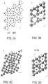
- FIG. 1A illustrates a comparison between measured XRD pattern data for rubidium doped tungsten oxide (Rb 0.29 WO 3 ) nanocrystals that were synthesized and XRD pattern data published in the Inorganic Crystal Structure Database (ICSD) as ICSD: 1716.
- FIG. 1A also includes an inset transmission electron microscopy (TEM) image of the synthesized Rb 0.29 WO 3 nanocrystals.
- FIG. 1B shows the absorbance spectra of a tungsten oxide material (WO 2.72 ), the structure of which is based on XRD pattern data, and of the tungsten oxide material doped with rubidium, sodium, and cerium.
- Cs x WO 3 may be a preferred tungsten bronze.
- the following procedures describe methods for creating Cs x WO 3 and analyzing its geometry, size, and dielectric environment for systematically manipulating optical properties
- the reaction was cooled to room temperature and 0.5 mL toluene (Aldrich) was added to the blue-green solution. A 1:1 ratio of acetone to reaction mixture precipitated the product and the mixture was centrifuged at 3800 rpm for ten minutes. The blue-green precipitate was redispersed in 0.5 mL toluene and precipitated again with 1 mL acetone (BDH). Centrifuging for an additional ten minutes at 3800 rpm resulted in clean nanocrystals of Cs x WO 3 .
- the reaction yields a qualitatively similar product over a range of CsCl (0.05-0.18 mmol) while varying the amounts of OlAm and OlAc results in three different nanocrystalline shapes (pseudo-spheres, 1.5 mmol OlAm and 3.1-7.9 mmol OlAc; truncated cubes, 0.50-1.0 mmol OlAm and 19.0 mmol OlAc; hexagonal prisms, 0.60-1.5 mmol OlAm and 19.0-31.7 mmol OlAc).
- XRD patterns were collected on a Bruker D8-Discover X-ray diffractometer equipped with a GADDS area detector and operated at 40 kV and 20 mA at the wavelength of Cu K ⁇ 1.54 ⁇ .
- Optical spectra were collected on an ASD LabSpec Pro and high resolution TEM images were collected on a JEOL 2100 operated at an accelerating voltage of 200kV.
- XRD modeling was performed using diffraction data for Cs 0x WO 3 (P6 3 22 space group) in CrystalMaker and Le Bail refinement was performed using the Generalized Structure Analysis System (GSAS).
- GSAS Generalized Structure Analysis System
- XPS X-ray Photoelectron Spectroscopy
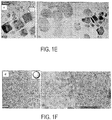
- FIG. 1C is a TEM image of WO 2.72 nanorods that were produced absent any cesium doping, with an inset illustrated rod shape. It has been previously observed in CeO 2 and Re 2 O 3 that changing the ratio of OlAc to OlAm provides shape control as a result of different binding capabilities of the ligands and passivation into the surface of the nanocrystal. Similarly, when cesium was incorporated, increasing the amount of OlAc produces more faceted shapes. As shown in FIGs. 1D-1F , different shapes were achieved depending on the ratio of OlAc to OlAm. Specifically, FIGs.
- 1D-1F are TEM images of Cs x WO 3 hexagonal prisms, cubes and pseudo-spheres, respectively, each with a corresponding inset illustrated shape.
- Hexagonal prisms result when the OlAc:OlAm ratio is 12.5-31, truncated cubes when the ratio is 5.2-12.5, and pseudo-spheres when the ratio is 2.1-5.2.
- FIG. 1G illustrates XRD patterns for samples synthesized using 0 mmol OlAc: 10.6 mmol OlAm and 10.6 mmol OlAc:O mmol OlAm with simulated data for Cs 0.29 WO 3 (ICSD: 56223), CsW 2 O 6 [Cs 0.5 WO 3 ] (ICSD: 72634.), and WO 3 (ICSD: 32001), which are not phase pure at these extremes of the surfactant composition.
- an OlAc:OlAm ratio of less than 2.1 or greater than 31.3 results in mixed crystalline phases by XRD.
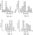
- Particle sizes were determined by TEM to be 16.0 ⁇ 5.8 nm for the undoped WO 2.72 rods (measuring the long dimension), 4.6 ⁇ 0.79 nm for the Cs x WO 3 pseudo-spheres, 20.4+2.4 nm for truncated cubes, and 13.2+3.0 nm for hexagonal prisms.
- the truncated cube particles included a variety of smaller sizes (under 12 nm) besides the primary product that were omitted from size measurements.
- FIG. 1H-1K are size histograms showing data collected from bright field TEM images including 50-100 particles each of undoped WO 2.72 rods, Cs 0.29 WO 3 hexagonal prisms, Cs 0.29 WO 3 truncated cubes, and Cs 0.29 WO 3 pseudo-spheres, respectively.
- FIG. 1L is a scanning electron microscopy (SEM) image of Cs 0.29 WO 3 hexagonal prisms.
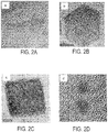
- FIG. 2A is a high resolution lattice-resolved TEM image of undoped WO 2.72 rods with a [-2 4 1] zone axis.
- FIG. 2B is a high resolution lattice-resolved TEM image of a Cs 0.29 WO 3 hexagonal prism viewed perpendicular to its largest face with a [-1 0 1] zone axis.
- FIG. 2C is a high resolution lattice-resolved TEM image of a truncated cube with a [1 0 0] zone axis.
- FIG. 2D is a high resolution lattice-resolved TEM image of pseudo-spheres with a [1 0 0] zone axis.
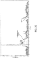
- FIG. 2E is an XRD pattern for WO 2.72 compared to a bulk reference pattern (ICSD: 24731).
- undoped tungsten oxide is consistent with monoclinic WO 2.72 , supporting the assignment of the composition as WO 3-x where x is 0.28.
- the WO 3-x structure is a reduced form of cubic WO 3 that contains oxygen vacancies within the crystal lattice. These oxygen vacancies create a distribution of W formal oxidation states between 6+, 5+, and 4+, and the alterations in charge state are responsible for changes in absorption properties compared to WO 3 . This is apparent by the dark blue color of the nanorods, which results from the tail of the strong infrared spectrum absorption crossing into the red edge of the visible spectrum.
- WO 3 may be described as a modification of the perovskite-type ABO 3 lattice in which the B site is occupied by W atoms and the A site is unoccupied, as shown in FIG. 3A , which is a ball-and-stick model of WO 3 . Oxygen vacancies within the lattice result in the formation of WO 6 octahedron as the basic structural unit.
- FIG. 3B is a polyhedral model of WO 3 , which shows that these oxygen vacancies are responsible for creating tunnels within the crystal structure of WO 2.72 .
- FIG. 3C is a polyhedral model of WO 2.72 showing that additional oxygen vacancies distort the WO 6 octahedral units and the local environments of the tungsten ions become heterogeneous. Doping with Cs + ions instead results in occupation of the open channels in the WO 3 structure to form Cs x WO 3 . This is shown in FIG. 3D , which is a polyhedral model of Cs x WO 3 .
- FIG. 3E shows XRD patterns for Cs 0.29 WO 3 spheres, truncated cubes, and hexagonal prisms.
- the three shapes of cesium tungsten bronze i.e., hexagonal prism, truncated cube, and pseudo-sphere
- XRD patterns were refined by Le Bail fitting in the GSAS suite for the hexagonal prisms (Rp 0.2091; wRp 0.1101) and truncated cubes (Rp 0.1485; wRp 0.0984).
- FIG. 3F is a Le Bail fit with residual plot of a 20.4 ⁇ 2.4 nm truncated cubes.
- FIG. 3G is a Le Bail fit with residual plot of 13.2 ⁇ 3.0 nm hexagonal prisms. The unit cell increases slightly in size when comparing the truncated cube to the hexagonal prism, with respective increases from 7.395 ⁇ to 7.404 ⁇ for the pattern shown in FIGs. 3E and 3F , and 7.606 ⁇ to 7.615 ⁇ for the pattern shown in FIG. 3G .
- FIG. 3H shows a survey scan in FIG. 3H.
- FIGs. 3I and 3J are high resolution scans of Cs 0.29 WO 3 showing normalized peak area measurements for tungsten and cesium respectively.
- FIG. 3K is a table detailing peak fit parameters and composition analysis for Cs 0.29 WO 3 .
- FIG. 4A illustrates the absorbance spectra of the hexagonal prism Cs 0.29 WO 3 in these solvents, showing two distinct absorbance peaks. While the longer wavelength peak is too broad to draw any definitive conclusions as to the peak shift, there is an obvious red-shift in the shorter wavelength peak as RI changes.
- FIG. 4B is a magnification of the shorter wavelength absorbance peak for the hexagonal prism Cs 0.29 WO 3 in TCE, DMF and MeCN.
- FIG. 4C is a plot showing solvent RI versus wavelength for the hexagonal prism Cs 0.29 WO 3 .
- Re ⁇ 1 ⁇ ⁇ p 2 ⁇ 2 + ⁇ 2
- ⁇ p the plasmon frequency of the bulk metal
- ⁇ represents frequency of incident light
- ⁇ damping frequency of bulk material
- Equation 1 ⁇ p 2 ⁇ med + 1
- FIG. 4D shows SPR peak position of experimental data and the theoretical prediction using Mie's solution to Maxwell's equation plotted against the RI of the surround medium (theory) or solvent (experiment).
- the data show that Mie's solution to Maxwell's equation predicts a stronger dependence of the peak wavelength on RI than was observed experimentally. This difference can be ascribed to the non-spherical shape of the particles as well as the contribution of the ligands attached to the surface of the nanocrystals.
- Noguez discusses SPRs for a series of silver nanoparticle shapes, explaining how the optical peaks change when increasing the number of truncations of a cube (see C. Noguez, J. Phys. Chem C., 2007, 111, 3806-3819 ). That is, truncating a cube results in shapes with different numbers of planes or faces; cube (6 faces), truncated cube (14 faces), icosohedron (20 faces), and sphere (infinite faces). As the number of faces on the particle increases, three important trends are apparent in the resonance spectra. First, the main/largest resonance will blue-shift. Second, the peaks with smaller wavelength resonances move closer to the main resonance and can be hidden. Third, the width of the main resonance peak increases.
- FIG. 5A shows flat projections of a hexagonal prism and truncated cube, with eight and ten faces respectively (a sphere has an infinite number of faces so is not depicted).
- FIG. 5B shows the absorbance spectra of Cs x WO 3 hexagonal prisms (top line), truncated cubes (second from top line), pseudo-spheres (second from bottom line), and WO 2.72 rods (bottom line), with spectra offset for clarity.
- the hexagonal prism has two distinct absorbance peaks, a less intense peak at 860 nm (peak 1) and a more intense peak at 1602 nm (peak 2).
- peak 1 As the number of faces on the nanocrystal surface increases from eight (hexagonal prism) to ten (truncated cube) to infinity (sphere), the optical peaks reduce from two obvious, distinct peaks to one. This is observed as the number of faces increase with a red-shift of peak 1 (respectively 860 nm, 990 nm, 1315 nm) and a blue-shift of peak 2 (respectively 1602 nm, 1506 nm, and 1315 nm). As the trend of increasing the faces of the particles progresses, peak 1 becomes less visible. In effect, peak 1 in the pseudo-sphere sample becomes indistinguishable from peak 2, so that both resonances occur under the envelope of one broader peak.
- FIG. 5B shows the absorbance spectra of WO 2.72 with a broad peak at approximately 2100 nm. This spectrum is sharply contrasted with those that result from doping with cesium, which changes the crystal structure from monoclinic to hexagonal.
- Adachi has suggested that peak 2 in Cs x WO 3 is a shift of the polaron seen in WO 2.72 (see K. Adachi et al., J. Mater. Res. 2012, 27, 965-970 ).
- Doped plasmonic materials have substantially lower carrier densities, such as Cu 1.85 Se with a carrier density of 3.0 x 1021cm -3 and indium tin oxide with a density of 1.9 x 1021 cm -3 .
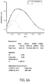
- the carrier density for the synthesized faceted Cs x WO 3 particles cannot be rigorously derived from their optical spectra without detailed electromagnetic modeling, but it was approximated by Drude theory to be as high as 5 x 1021cm -3 .
- FIG. 6A illustrates Gaussian peak fit of pseudo sphere absorbance spectra including calculated parameters, statistics, and calculated carrier density.
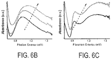
- FIG. 6B shows the absorbance spectra of a Cs x WO 3 pseudo-sphere sample, with aliquots of the same reaction taken at 5 mins (bottom line), 30 mins (middle line), and 60 mins (top line). As the reaction progresses the particle size increases from roughly 3 nm to 5 nm, and there is an obvious red-shift of the resonance peak from 1081 nm at 5 min to 1350 nm at 60 min.
- FIG. 6A illustrates Gaussian peak fit of pseudo sphere absorbance spectra including calculated parameters, statistics, and calculated carrier density.
- FIG. 6B shows the absorbance spectra of a Cs x WO 3 pseudo-sphere sample, with aliquots of the same reaction taken at 5 mins (bottom line), 30 mins (middle line), and 60 mins (top line). As the reaction progresses the particle size increases from
- 6C shows the absorbance spectra of a Cs x WO 3 hexagonal prism sample, with aliquots of the same reaction taken at 30 mins (bottom line) and 90 mins (top line). As the reaction progresses from 30 min to 90 min the plasmon peaks shift from 835 nm to 870 nm and 1840 m to 1962 nm. These shifts in spectra follow the same qualitative trends reported in the literature for 5-40 nm gold rods (with fixed 2.4 aspect ratio), and 9-99 nm gold spheres.
Landscapes
- Physics & Mathematics (AREA)
- Nonlinear Science (AREA)
- Chemical & Material Sciences (AREA)
- Inorganic Chemistry (AREA)
- General Physics & Mathematics (AREA)
- Optics & Photonics (AREA)
- Crystallography & Structural Chemistry (AREA)
- Electrochromic Elements, Electrophoresis, Or Variable Reflection Or Absorption Elements (AREA)
Description
- This invention was made with government support under Contract No. DE-AC02-05CH11231 awarded by the U.S. Department of Energy. The government has certain rights in this invention.
- The present invention is generally directed to electrochromic devices, and more particularly to the selectively modulating transmittance of radiation as a function of voltage applied to a nanostructured material in an electrochromic device.
- Residential and commercial buildings represent a prime opportunity to improve energy efficiency and sustainability in the United States. The buildings sector alone accounts for 40% of the United States' yearly energy consumption (40 quadrillion BTUs, or "quads", out of 100 total), and 8% of the world's energy use. Lighting and thermal management each represent about 30% of the energy used within a typical building, which corresponds to around twelve quads each of yearly energy consumption in the US. Windows cover an estimated area of about 2,500 square km in the US and are a critical component of building energy efficiency as they strongly affect the amount of natural light and solar gain that enters a building. Recent progress has been made toward improving window energy efficiency through the use of inexpensive static coatings that either retain heat in cold climates (low emissive films) or reject solar heat gain in warm climates (near-infrared rejection films).
- Currently, static window coatings can be manufactured at relatively low cost. However, these window coatings are static and not well suited for locations with varying climates. An electrochromic (EC) window coating overcomes these limitations by enhancing the window performance in all climates. EC window coatings undergo a reversible change in optical properties when driven by an applied potential. Traditional EC materials, such as WO3, Nb2O5, and NiO, primarily modulate visible light (400-780 nm), while the near-infrared (NIR) region of light (780-2500 nm) remains either unchanged or switches simultaneously with visible region of light.
- The publication of Sabine Heusing ("A contribution to climate protection - electrochromic windows fabricated with the sol-gel technology", Annual report Jahresbericht of Leibniz Institut für Neue Materialien Ein Institut der Leibniz-Gemeinschaft, pages 90 - 99) refers to electrochromic windows fabricated with sol-gel technology based on compositions of Na3AlF6, ZrSiO4, and InSb. Not disclosed is a nanostructured transition metal oxide bronze, which selectively modulates transmittance of near-infrared (NIR) spectrum radiation and visible spectrum radiation as a function of an applied voltage to the device, wherein one or more dopant comprises at least one of a dopant species or an intercalation species as defined in the claims of the present application.
-
US4325611 (A ) discloses an electrooptical device comprising an optically transparent substrate, an optically transparent electrode formed on a surface of said substrate, a specific second electrode in spaced alignment with said optically transparent electrode, an electrochromic material supported by said substrate and positioned between said electrodes, said electrochromic material comprising an oxide of at least one transition metal having the hexagonal tungsten bronze crystal structure, an electrolyte between and contacting said electrochromic material and said second electrode, said electrolyte being conductive of ions of said electroactive material between said second electrode and the crystal structure of said electrochromic material, and an ionic species in said crystal structure of said electrochromic material whereby said electrochromic material changes color when ions of said electroactive material are in said crystal structure. -
US2013107345 (A1 ) discloses a method of fabricating an electrochromic device, the method comprising: a. depositing a first portion of a metal oxide layer; b. lithiating the first portion with elemental lithium; and c. depositing a second portion of the metal oxide layer. Like the publication of Sabine Heusing,US2013107345 (A1 ) does not disclose said nanostructured transition metal oxide bronze, wherein one or more dopants comprise the species as defined in the claims of the present application. -
US2007187653 (A1 ) discloses a visible light transmitting particle-dispersed electrical conductor, which is a plural aggregate of specific electroconductive particles composed of a tungsten oxide expressed by the general formula WyOz (where W is tungsten, O is oxygen, and 2.2≤z/y≤2.999), and/or a composite tungsten oxide expressed by the general formula MxWyOz (where M is one or more specific elements; O is oxygen; 0.001≤x/y≤1.1; and 2.2≤z/y≤3.0). -
US2013286458 (A1 ) discloses an electrochemical device having at least one of electrically controllable optical or energy transmission properties comprising: - a substrate; a functional system formed on the substrate and comprising:
- a bottom electrode coating formed on the substrate; a top electrode coating formed on the bottom electrode coating; and at least one specific electrochemically active film located between the bottom electrode coating and the top electrode coating; and
- a specific cover film formed on the functional system and in which the device comprises electrical connection means arranged at least partially in at least one surface cavity for electrical contact with the top electrode coating. Like the publication of Sabine Heusing,
US2013286458 (A1 ) does not disclose said nanostructured transition metal oxide bronze, wherein one or more dopants comprise the species as defined in the claims of the present application. - The invention refers to an electrochromic window (100) comprising:
- at least one transparent conductor layer (102a, 102b);
- a nanostructured transition metal oxide bronze layer (112) comprising: one or more transition metal oxide comprising at least one of niobium, tungsten, molybdenum, vanadium, and titanium oxide, and one or more dopant; a solid state electrolyte (106); and a counter electrode (108),
- wherein the nanostructured transition metal oxide bronze (112) independently, selectively modulates transmittance of near-infrared (NIR) spectrum radiation and visible spectrum radiation as a function of an applied voltage to the device,
- wherein the one or more dopant comprises at least one of:
- a dopant species that causes a surface plasmon resonance effect on the one or more transition metal oxide by creating delocalized electron carriers that selectively modulate transmittance of NIR spectrum radiation in response to a first applied voltage to the device, the dopant species comprising at least one of cesium, cerium, lanthanum, praseodymium, neodymium, promethium, samarium, europium, gadolinium, terbium, dysprosium, holmium, erbium, thulium, ytterbium, lutetium, and rubidium ions; and
- an intercalation species that causes a change in the oxidation state of transition metal ions in the transition metal oxide due to intercalation into and deintercalation from the metal oxide, which selectively modulates transmittance of visible spectrum radiation in response to a second applied voltage to the device, wherein the second applied voltage has a larger absolute value than the first applied voltage, the intercalation species comprising at least one of an intercalation species comprising at least one of lithium, sodium, potassium, rubidium, cesium, beryllium, magnesium, calcium, strontium, barium ions, cerium, lanthanum, praseodymium, neodymium, promethium, samarium, europium, gadolinium, terbium, dysprosium, holmium, erbium, thulium, ytterbium, or lutetium ions; and a charged proton species.
- The invention further refers to a method of operating an electrochromic window as defined in the claims as well as to the use of an electrochromic device for enhancing optical changes in windows as defined in the claims.
-
-
FIG. 1A is a graph showing measured and published x-ray diffraction patterns for Rb0.29WO3 with an inset transmission electron microscopy (TEM) image of synthesized nanocrystals. -
FIG. 1B is a graph showing absorbance spectra of various doped WO2.72 compositions. -
FIGs. 1C-1F are TEM images of different shapes of nanostructures for WO2.72 and/or Cs0.29WO3 samples. -
FIG. 1G is a graph showing x-ray diffraction patterns for various synthesized samples and simulated compounds. -
FIGs. 1H-1K are size histograms from bright field TEM images including 50-100 particles each of different shapes for various samples. -
FIG. 1L is a scanning electron microscopy (SEM) image of hexagonal prisms for a sample. -
FIGs. 2A-2D are TEM images of different shapes of nanostructures for various samples. -
FIG. 2E is a graph showing x-ray diffraction patterns of a sample and of bulk reference pattern data. -
FIG. 3A is a ball-and-stick model crystal structure of a composition in various embodiments. -
FIGs. 3B-3D are polyhedral models of compositions of the various embodiments. -
FIGs. 3E-3G are graphs showing normalized x-ray diffraction patterns of a sample having various shapes. -
FIG. 3H is a graph showing results of an x-ray photoelectron spectroscopy (XPS) survey scan for samples of the embodiments. -
FIGs. 3I and 3J are high resolution scans of tungsten 4f7/2 and 4f5/2 peaks andcesium -
FIG. 3K is a table showing peak fit parameters and compositions for compositions of the embodiments. -
FIGs. 4A-4C are graphs showing absorbance spectra of hexagonal prism Cs0.29WO3 in solvents of varying refractive indexes. -
FIG. 4D is a plot showing experimental data and theoretical predictions for SPR peak position versus refractive index of spherical nanoparticles. -
FIG. 5A is an illustration of different faceted shapes of nanocrystals and their flat projections that may exist in the various embodiments. -
FIG. 5B is a graph showing absorbance spectra for samples having different shapes in the various embodiments. -
FIG. 6A is a graph showing absorbance spectra for peak fit of pseudo-sphere absorbance spectra including calculated parameters, statistics, and calculated carrier density. -
FIGs. 6B-6C are absorbance spectra of progressing reactions for samples having different shapes in the various embodiments. -
FIG. 7 is a schematic representation of an electrochromic device according to various embodiments. - The invention refers to an electrochromic window as defined in the claims. In order to improve the performance of EC window coatings, selective modulation of both NIR spectrum and visible spectrum radiation is desired.
- Based on the applied potential, the materials may modulate NIR spectrum radiation (wavelength of 780-2500 nm), as well as visible spectrum radiation (wavelength of 400-780 nm). In an example, the material may operate in multiple selective modes based on the applied potential. Control of the individual operating modes may occur at different applied bias, allowing users the capability of achieving thermal management within buildings and other enclosures (e.g., vehicles, etc.), while still providing shading when desired.
-
FIG. 7 illustrates an embodiment electrochromic device. Thedevice 100 includes a firsttransparent conductor layer 102a, a workingelectrode 104, asolid state electrolyte 106, acounter electrode 108, and a secondtransparent conductor layer 102b. Some embodiment electrochromic devices, may also include one or more optically transparent support layer, such as plastic orglass layer 110 positioned in front of the firsttransparent conductor layer 102a and/or positioned behind the secondtransparent conductor layer 102b. - It should be noted that the
electrochromic device 100 may be oriented upside down or sideways from the orientation illustrated inFIG. 1 . Furthermore, the thickness of the layers and/or size of the components of thedevice 100 are not drawn to scale or in actual proportion to one another other, but rather are shown as representations. - The first and second
transparent conductor layers transparent conductor layers transparent conductor layers - In the various embodiments, the working
electrode 104 may includenanostructures 112 of a doped transition metal oxide bronze. As discussed above, the thickness of the layers of thedevice 100, including and the shape, size and scale of nanostructures is not drawn to scale or in actual proportion to each other, but is represented for clarity. In the various embodiments,nanostructures 112 may be embedded in an optically transparent matrix material or provided as a packed or loose layer of nanostructures exposed to the electrolyte. - In the various embodiments, the doped transition metal oxide bronze of the
nanostructures 112 may be a ternary composition of the type AxMzOy, where M represents a transition metal ion species in at least one transition metal oxide, and A represents at least one dopant as defined in the claims. Transition metal oxides that are used in the invention include niobium oxide, tungsten oxide, molybdenum oxide, vanadium oxide, and titanium oxide. In one example, the nanostructured transition metal oxide bronze may include a plurality of tungsten oxide (WO3-x) nanoparticles, where 0 ≤ x ≤ 0.33, such as 0 ≤ x ≤ 0.1. - In various embodiments, the at least one dopant species comprises a first dopant species that, upon application of a particular first voltage range, causes a first optical response. The applied voltage may be, for example, a negative bias voltage. Specifically, the first dopant species may cause a surface plasmon resonance effect on the transition metal oxide by creating a significant population of delocalized electronic carriers. Such surface plasmon resonance may cause absorbance of NIR spectrum radiation, the specific amount and wavelengths for which may be varied/adjusted based on other factors (e.g., nanostructure shape, size, etc.), discussed in further detail below. According to the invention, the first dopant species is an ion species selected from the group of cesium, rubidium, cerium, lanthanum, praseodymium, neodymium, promethium, samarium, europium, gadolinium, terbium, dysprosium, holmium, erbium, thulium, ytterbium, and lutetium.
- In various embodiments, the dopant may include a second dopant species that causes a second optical response based upon application of a voltage within a different, second particular range. The applied voltage may be, for example, a negative bias voltage. In an embodiment, the second dopant species may migrate between the
solid state electrolyte 106 and the nanostructured transition metal oxide bronze of the workingelectrode 104 as a result of the applied voltage. Specifically, the application of voltage within the particular range may cause the second dopant species to intercalate and deintercalate the transition metal oxide structure. In this manner, the second dopant may cause a change in the oxidation state of the transition metal oxide, which may cause a polaron effect and a shift in the lattice structure of the transition metal oxide. This shift may cause absorption of both visible and NIR spectrum radiation. - According to the invention, the second dopant species is an intercalation ion species selected from the group of cerium, lanthanum, praseodymium, neodymium, promethium, samarium, europium, gadolinium, terbium, dysprosium, holmium, erbium, thulium, ytterbium, and lutetium, lithium, sodium, potassium, rubidium, cesium, beryllium, magnesium, calcium, strontium, and barium. In other embodiments, the second dopant species may include a charged proton species.
- Based on these optical effects, the
nanostructures 112 of the working electrode may progressively modulate transmittance of NIR and visible light as a function of applied voltage by operating in at least three different modes. For example, a first mode may be a highly solar transparent ("bright") mode in which the workingelectrode 104 is transparent to NIR spectrum and visible spectrum radiation. A second mode may be selective-NIR blocking ("cool") mode in which the workingelectrode 104 is transparent to visible spectrum radiation but absorbs NIR spectrum radiation. A third mode may be a visible blocking ("dark") mode in which the workingelectrode 104 absorbs both visible spectrum and at least some of NIR spectrum radiation. In an example, application of a first voltage having a negative bias may cause the electrochromic device to operate in the cool state, blocking transmittance of NIR spectrum radiation. In another example, application of a second negative bias voltage having a higher absolute value than the first voltage may cause the electrochromic device to operate in the dark state, blocking transmittance of visible spectrum and NIR spectrum radiation. In another example, application of a third voltage having a positive bias may cause the electrochromic device to operate in the bright state, allowing transmittance of both NIR spectrum and visible spectrum radiation. In various embodiments, the applied voltage may be between -5V and 5V, preferably between -2V and 2V. For example, the first voltage may be -0.25V to -0.75V, and the second voltage may be -1V to -2V. In another example, the absorption of radiation at a wavelength of 800-1500 nm by the electrochromic device may be at least 50% greater than its absorption of radiation at a wavelength of 450-600 nm. - In various embodiments, the
solid state electrolyte 106 may include at least a polymer material and a plasticizer material, such that electrolyte may permeate into crevices between thenanoparticles 112 of the nanostructured transition metal oxide bronze material. In some embodiments, thesolid state electrolyte 106 may further include a salt, for example, a lithium salt. In some embodiments, thesolid state electrolyte 106 may initially contain a solvent, such as butanol, which may be evaporated off once the electrochromic device is assembled. In some embodiments, thesolid state electrolyte 106 may be around 40-60 wt% plasticizer material, preferably around 50-55 wt% plasticizer material. In an embodiment, the plasticizer material may include at least one of tetraglyme and an alkyl hydroperoxide. In an embodiment, the polymer material of thesolid state electrolyte 106 may be polyvinylbutyral (PVB), and the salt may be lithium bis(trifluoromethane). In other embodiments, thesolid state electrolyte 106 may include at least one of lithium phosphorus oxynitride (LiPON) and tantalum pentoxide (Ta2O5). - The
counter electrode 108 of the various embodiments should be capable of storing enough charge to sufficiently balance the charge needed to cause visible tinting to the nanostructured transition metal oxidebronze working electrode 104. In various embodiments, thecounter electrode 108 may be formed as a conventional, single component film, a nanostructured film, or a nanocomposite layer. - In some embodiments, the
counter electrode 108 may be formed from at least one passive material that is optically transparent to both visible spectrum and NIR spectrum radiation during the applied biases. Examples of such passive counter electrode materials may include CeO2, CeVO2, TiO2, indium tin oxide, indium oxide, tin oxide, manganese or antimony doped tin oxide, aluminum doped zinc oxide, zinc oxide, gallium zinc oxide, indium gallium zinc oxide, molybdenum doped indium oxide, Fe2O3, or V2O5. In other embodiments thecounter electrode 108 may be formed from at least one complementary material, which may be transparent to NIR spectrum radiation but which may be oxidized in response to application of a bias, thereby causing absorption of visible spectrum radiation. Examples of such complementary counter electrode materials may include Cr2O3, MnO2, FeO2, CoO2, NiO2, RhO2, or IrO2. - Without being bound to any particular theory, it is believed that the application of a first voltage in the various embodiments may cause the interstitial dopant species (e.g., cesium) in the crystal structure of the transition metal oxide bronze to have a greater amount of free carrier electrons and/or to cause the interstitial dopant species (e.g., lithium ions from the electrolyte) to perform non-faradaic capacitive or pseudo-capacitive charge transfer on the surface of the
nanostructures 112, which may cause the surface plasmon resonance effect to increase the absorption of near-infrared radiation. In this manner, the absorption properties of the transition metal oxide bronze characteristics may change (i.e., increased absorption of near-infrared spectrum radiation) upon application of the first voltage. Further, application of a second voltage having a higher absolute value than the first voltage in the various embodiments may cause faradaic intercalation of an intercalation dopant species (e.g., lithium ions) from the electrolyte into the transition metal oxide nanostructures. It is believed that the interaction of this dopant species provides interstitial dopant atoms in the lattice which creates a polaron effect. In this manner, the lattice structure of transition metal oxide nanocrystals may experience a polaron type shift, thereby altering its absorption characteristics (i.e., shift to visible spectrum radiation absorption) to block both visible and near infrared radiation. - Compared to nanocomposite electrochromic films, the various embodiments may involve similar production by utilizing a single nanostructured material in the working electrode to achieve the desired spectral control in both near-infrared spectrum and visible spectrum ranges.
- The nanostructured transition metal oxide bronzes that may be used to form the working
electrode 104 of embodiment electrochromic devices maybe formed using any of a number of low cost solution process methodologies. For example, solutions of Nb:TiO2 and CsxWO3 may be synthesized using colloidal techniques. Compared to other synthetic methodologies, colloidal synthesis may offer a large amount of control over the nanostructure size, shape, and composition of the nanostructured transition metal oxide bronze. After deposition, a nanostructured transition metal oxide bronze material in the workingelectrode 104 may be subjected to a thermal post treatment in air to remove and cap ligands on the surface of the nanostructures. - Electrochromic responses of prepared nanostructured transition metal oxide bronze materials (e.g., CsxWO3, Nb:TiO2, etc.) may be demonstrated by spectroelectrochemical measurements.
- In various embodiments, the shape, size, and doping levels of nanostructured transition metal oxide bronzes may be tuned to further contribute to the spectral response by the device. For instance, the use of rod versus
spherical nanostructures 112 may provide a wider level of porosity, which may enhance the switching kinetics. Further, a different range of dynamic plasmonic control may occur for nanostructures with multiple facets, such as at least 20 facets. - Various embodiments may also involve alternation of the
nanostructures 112 that form the workingelectrode 104. For example, the nanostructures may be nanoparticles of various shapes, sizes and/or other characteristics that may influence the absorbance of NIR spectrum and/or visible spectrum radiation. In some embodiments, thenanostructures 112 may be isohedrons that have multiple facets, preferably at least 20 facets. - The following examples, experimental methods and results are not intended to limit the scope of the invention, but rather are provided merely for illustration of how nanoparticle characteristics may be utilized to further tune their electrochromic properties.
- Localized surface plasmon resonance phenomena have recently been investigated in unconventional plasmonic materials such as metal oxide and chalcogenide semiconductors doped with high concentrations of free carriers. Colloidal nanocrystals of CsxWO3 a tungsten bronze in which electronic charge carriers are introduced by interstitial doping, were synthesized. By using varying ratios of oleylamine to oleic acid three distinct shapes of these nanocrystals may be formed; hexagonal prisms, truncated cubes, and pseudo-spheres, which may exhibit strongly shape-dependent absorption features in the near infrared region. As shown in results, lower symmetry shapes may correlate with sharper plasmon resonance features and more distinct resonance peaks. The plasmon peak positions may also shift systematically with size and with the dielectric constant of the surrounding media, reminiscent of typical properties of plasmonic metal nanoparticles.
- Controlling the size and geometry of metal nanocrystal surfaces may make it possible to tailor these particles to achieve diverse surface plasmon resonance (SPR) properties, allowing select nanoparticles to be tuned for use in sensors, electronic circuits, and photonic devices. The influence of particle geometry and size on optical properties is documented for many different metal nanoparticle shapes, including cubes, octahedra, rods, and stars. Semiconductor nanocrystals may offer similar synthetic control over size and geometry. The shape of such nanocrystals dramatically influences their near infrared (NIR) optical spectra. Changing the shape of a metallic particle alters the surface polarization, which influences how the surface interacts with light and thus the SPR. Particle size also has an effect on the optical properties of these materials, which is often described using Mie's solution to Maxwell's equation or the discrete dipole approximation.
- Though exact solutions only exist for spheres, spheroids, and infinite cylinders, changing the nanoparticle size of a wide variety of shapes is known to influence the SPR. For example, increasing the aspect ratio in nanorods may cause the plasmon peak to red-shift in samples of gold as well as tungsten oxide. Increasing the size of silver triangles and plates may also result in a red-shift of the SPR.
- Until recently, semiconductor nanocrystals had low free carrier concentrations and did not exhibit SPR phenomena. In metal oxide nanocrystals, substitutional doping with heterovalent metal ions has recently been used to introduce large free electron populations that support SPR in the infrared region. For example, this phenomenon has recently been demonstrated in tin-doped indium oxide, aluminum-doped zinc oxide, indium-doped cadmium oxide, and niobium-doped anatase titania. In copper chalcogenide nanocrystals large populations of free holes are generated by inducing copper deficiencies, which yields similar infrared plasmon absorption features. However, these defect-doping strategies are limited with respect to the achievable carrier concentrations and therefore the spectral tuning range of the SPR.
- Tungsten oxide of the formula WO3-x (x<0.33) is a reduced form of tungsten trioxide (WO3) that is widely understood to contain oxygen vacancies within the crystal lattice. These oxygen vacancies create changes in the charge states of tungsten, which influence absorption properties and can give rise to infrared SPR phenomena. However, the crystal structure of WO3 may offer additional opportunity for introducing free electrons beyond the concentrations typically achievable by defect mechanisms. Unlike substitutional doping, in which a doping atom replaces an atom within the crystal lattice, interstitial doping allows a new atom to be incorporated within the crystal structure as a result of atomic vacancies or defects within the lattice. As a result, it is possible for the nanocrystal to have a higher concentration of free electrons. The crystal structures of WO3 and WO3-x are composed of WO6 octahedra as the basic structural unit, creating one-dimensional tunnels of variable sizes and shapes. These tunnels are highly selective for cations with ionic radii of 1.2 and 1.7Å, so they are ideal for the incorporation of cesium atoms with ionic radii of 1.69Å. Such cesium-doped tungsten oxides are known to have exceptionally strong NIR spectrum radiation absorption because the cesium may act as an interstitial dopant, introducing a far higher population of free electrons than is achievable using lattice-site defects including heterovalent metals or vacancies.
- A class of interstitially doped tungsten oxides known as tungsten bronze has the formula MxWO3, where M may be, without limitation, Li+, Na+, Cs+, or Rb+. Tungsten bronze materials retain a high transmittance of visible light while exhibiting high absorption of NIR spectrum radiation, making them ideal candidates for spectrally-selective optical devices, such as electrochromic smart windows. Various methods have been used to synthesize MxWO3, such as solid-state synthesis, thermal plasma synthesis, and chemical transport. Various embodiment methods may involve colloidal synthesis of tungsten bronze, which may show how shape evolution from pseudo-spheres to truncated cubes to hexagonal prisms of the same CsxWO3 crystal structure influences the SPR.
- X-ray diffraction (XRD) confirms that these synthetic procedures may be translated to synthesize RbxWO3. As shown in
FIGs. 1A and1B , using cerium and sodium as dopants may also influence the NIR optical spectra.FIG. 1A illustrates a comparison between measured XRD pattern data for rubidium doped tungsten oxide (Rb0.29WO3) nanocrystals that were synthesized and XRD pattern data published in the Inorganic Crystal Structure Database (ICSD) as ICSD: 1716.FIG. 1A also includes an inset transmission electron microscopy (TEM) image of the synthesized Rb0.29WO3 nanocrystals.FIG. 1B shows the absorbance spectra of a tungsten oxide material (WO2.72), the structure of which is based on XRD pattern data, and of the tungsten oxide material doped with rubidium, sodium, and cerium. - The preferred incorporation of ions, the size of cesium and the exceptional NIR spectrum radiation absorption of tungsten oxide doped with cesium, indicate that CsxWO3 may be a preferred tungsten bronze. The following procedures describe methods for creating CsxWO3 and analyzing its geometry, size, and dielectric environment for systematically manipulating optical properties
- In a 50 mL three neck flask equipped with an air-cooled condenser, under nitrogen flow, 0.20 mmol (66 mg) tungsten (IV) chloride (WCl4) (Strem Chemical), 0.12 mmol (20 mg) cesium chloride (CsCl) (Aldrich), 0.60 mmol (0.20 mL) oleylamine (OlAm) (Aldrich), and 19.0 mmol (5.2 mL) oleic acid (OlAc) (Sigma-Aldrich) were stirred at 300°C for 120 minutes and resulted in a blue-green solution. The reaction was cooled to room temperature and 0.5 mL toluene (Aldrich) was added to the blue-green solution. A 1:1 ratio of acetone to reaction mixture precipitated the product and the mixture was centrifuged at 3800 rpm for ten minutes. The blue-green precipitate was redispersed in 0.5 mL toluene and precipitated again with 1 mL acetone (BDH). Centrifuging for an additional ten minutes at 3800 rpm resulted in clean nanocrystals of CsxWO3. The reaction yields a qualitatively similar product over a range of CsCl (0.05-0.18 mmol) while varying the amounts of OlAm and OlAc results in three different nanocrystalline shapes (pseudo-spheres, 1.5 mmol OlAm and 3.1-7.9 mmol OlAc; truncated cubes, 0.50-1.0 mmol OlAm and 19.0 mmol OlAc; hexagonal prisms, 0.60-1.5 mmol OlAm and 19.0-31.7 mmol OlAc).
- In a 50 mL, three-neck flask equipped with an air-cooled condenser, under nitrogen flow, 0.20 mmol (66 mg) WCl4, 19 mmol (1.2 mL) OlAm, and 1.5 mmol (3.5 mL) OlAc were stirred at 300°C for 120 minutes. The product was precipitated with 12 mL acetone and centrifuged for 15 minutes at 3800 rpm. The blue pellet was redispersed in 0.5 mL toluene and precipitated once more with 2 mL acetone. Centrifuging for 20 minutes at 3800 rpm resulted in a clean, dark blue product with nanorod morphology.
- XRD patterns were collected on a Bruker D8-Discover X-ray diffractometer equipped with a GADDS area detector and operated at 40 kV and 20 mA at the wavelength of Cu Kα 1.54Å. Optical spectra were collected on an ASD LabSpec Pro and high resolution TEM images were collected on a
JEOL 2100 operated at an accelerating voltage of 200kV. XRD modeling was performed using diffraction data for Cs0xWO3 (P6322 space group) in CrystalMaker and Le Bail refinement was performed using the Generalized Structure Analysis System (GSAS). X-ray Photoelectron Spectroscopy (XPS) measurements were performed using a Physical Electronics PHI 5400 equipped with an aluminum x-ray source. All XPS spectra were calibrated to the C1s peak at 284.8 eV in order to correct for possible charging and high resolution spectra of theCs 3d5/2 and W 4f peaks were analyzed using the CasaXPS software package. Elemental analysis using Flame Atomic Absorption (FLAA) and Inductively Coupled Plasma Optical Emission Spectrometry (ICP-OES) was performed by Galbraith Laboratories, Incorporated. Optical spectra were collected in tetrachloroethylene (TCE) (Sigma-Aldrich). - To evaluate the shape of the resulting nanocrystals, samples were surveyed by low-resolution TEM.
-
FIG. 1C is a TEM image of WO2.72 nanorods that were produced absent any cesium doping, with an inset illustrated rod shape. It has been previously observed in CeO2 and Re2O3 that changing the ratio of OlAc to OlAm provides shape control as a result of different binding capabilities of the ligands and passivation into the surface of the nanocrystal. Similarly, when cesium was incorporated, increasing the amount of OlAc produces more faceted shapes. As shown inFIGs. 1D-1F , different shapes were achieved depending on the ratio of OlAc to OlAm. Specifically,FIGs. 1D-1F are TEM images of CsxWO3 hexagonal prisms, cubes and pseudo-spheres, respectively, each with a corresponding inset illustrated shape. Hexagonal prisms result when the OlAc:OlAm ratio is 12.5-31, truncated cubes when the ratio is 5.2-12.5, and pseudo-spheres when the ratio is 2.1-5.2. -
FIG. 1G illustrates XRD patterns for samples synthesized using 0 mmol OlAc: 10.6 mmol OlAm and 10.6 mmol OlAc:O mmol OlAm with simulated data for Cs0.29WO3 (ICSD: 56223), CsW2O6 [Cs0.5WO3] (ICSD: 72634.), and WO3(ICSD: 32001), which are not phase pure at these extremes of the surfactant composition. As shown by the data, an OlAc:OlAm ratio of less than 2.1 or greater than 31.3 results in mixed crystalline phases by XRD. - Particle sizes were determined by TEM to be 16.0±5.8 nm for the undoped WO2.72 rods (measuring the long dimension), 4.6±0.79 nm for the CsxWO3 pseudo-spheres, 20.4+2.4 nm for truncated cubes, and 13.2+3.0 nm for hexagonal prisms. The truncated cube particles included a variety of smaller sizes (under 12 nm) besides the primary product that were omitted from size measurements.
-
FIG. 1H-1K are size histograms showing data collected from bright field TEM images including 50-100 particles each of undoped WO2.72 rods, Cs0.29WO3 hexagonal prisms, Cs0.29WO3 truncated cubes, and Cs0.29WO3 pseudo-spheres, respectively.FIG. 1L is a scanning electron microscopy (SEM) image of Cs0.29WO3 hexagonal prisms. - The faceted shapes observed by TEM suggest crystalline particles, and were confirmed to be single crystals by high resolution TEM as shown in
FIGs. 2A-2D. FIG. 2A is a high resolution lattice-resolved TEM image of undoped WO2.72 rods with a [-2 4 1] zone axis.FIG. 2B is a high resolution lattice-resolved TEM image of a Cs0.29WO3 hexagonal prism viewed perpendicular to its largest face with a [-1 0 1] zone axis.FIG. 2C is a high resolution lattice-resolved TEM image of a truncated cube with a [1 0 0] zone axis.FIG. 2D is a high resolution lattice-resolved TEM image of pseudo-spheres with a [1 0 0] zone axis. -
FIG. 2E is an XRD pattern for WO2.72 compared to a bulk reference pattern (ICSD: 24731). As shown, undoped tungsten oxide is consistent with monoclinic WO2.72, supporting the assignment of the composition as WO3-x where x is 0.28. The WO3-x structure is a reduced form of cubic WO3 that contains oxygen vacancies within the crystal lattice. These oxygen vacancies create a distribution of W formal oxidation states between 6+, 5+, and 4+, and the alterations in charge state are responsible for changes in absorption properties compared to WO3. This is apparent by the dark blue color of the nanorods, which results from the tail of the strong infrared spectrum absorption crossing into the red edge of the visible spectrum. - To better understand how NIR spectrum radiation plasmonic characteristics can emerge in interstitially doped tungsten bronze nanocrystals, it is useful to consider the crystallographic implications of doping tungsten oxide. WO3 may be described as a modification of the perovskite-type ABO3 lattice in which the B site is occupied by W atoms and the A site is unoccupied, as shown in
FIG. 3A , which is a ball-and-stick model of WO3. Oxygen vacancies within the lattice result in the formation of WO6 octahedron as the basic structural unit.FIG. 3B is a polyhedral model of WO3, which shows that these oxygen vacancies are responsible for creating tunnels within the crystal structure of WO2.72.FIG. 3C is a polyhedral model of WO2.72 showing that additional oxygen vacancies distort the WO6 octahedral units and the local environments of the tungsten ions become heterogeneous. Doping with Cs+ ions instead results in occupation of the open channels in the WO3 structure to form CsxWO3. This is shown inFIG. 3D , which is a polyhedral model of CsxWO3. -
FIG. 3E shows XRD patterns for Cs0.29WO3 spheres, truncated cubes, and hexagonal prisms. The three shapes of cesium tungsten bronze (i.e., hexagonal prism, truncated cube, and pseudo-sphere) were determined by XRD to be Cs0.29WO3, consistent with a Cs0.29WO3 reference pattern. XRD patterns were refined by Le Bail fitting in the GSAS suite for the hexagonal prisms (Rp 0.2091; wRp 0.1101) and truncated cubes (Rp 0.1485; wRp 0.0984).FIG. 3F is a Le Bail fit with residual plot of a 20.4±2.4 nm truncated cubes.FIG. 3G is a Le Bail fit with residual plot of 13.2±3.0 nm hexagonal prisms. The unit cell increases slightly in size when comparing the truncated cube to the hexagonal prism, with respective increases from 7.395 Å to 7.404 Å for the pattern shown inFIGs. 3E and 3F , and 7.606 Å to 7.615 Å for the pattern shown inFIG. 3G . - Though XRD confirms that Cs is incorporated within the crystal structure, further analysis was performed to determine how the Cs ions are distributed throughout the nanocrystals. Specifically, doping near the surface of the nanocrystals of Cs0.29WO3 was characterized by XPS, which is shown in a survey scan in
FIG. 3H. FIGs. 3I and 3J are high resolution scans of Cs0.29WO3 showing normalized peak area measurements for tungsten and cesium respectively. The surface composition was dominated by oxygen and carbon, with a metals composition determined to be 18.2% Cs and 81.7% W from the normalized peak area measurements (i.e. x = 0.15 in CsxWO3). By contrast, the average doping content analysis was determined by Inductively coupled plasma atomic emission spectroscopy (ICP-OES) and flame atomic absorption (FLAA) spectroscopy to be x = 0.09. These results suggest that the Cs distribution is radially nonuniform with higher doping levels near the surface of the nanocrystals.FIG. 3K is a table detailing peak fit parameters and composition analysis for Cs0.29WO3. - To investigate whether the NIR spectrum radiation absorbance of synthesized CsxWO3 nanocrystals can be ascribed to SPR or to absorption by local defect states, shift in the absorbance peak in solvents of varying refractive index (RI) was observed. The SPR is known to be sensitive to the RI of the surrounding environment, where increasing the RI of the solvent has a linear effect on the wavelength of the plasmon peak. Optical spectra of the same hexagonal prism sample of Cs0cWO3 were collected in solvents TCE, dimethylformamide (DMF) (Aldrich), and acetonitrile (MeCN), which have respective RIs of 1.51, 1.43, and 1.35.
-
FIG. 4A illustrates the absorbance spectra of the hexagonal prism Cs0.29WO3 in these solvents, showing two distinct absorbance peaks. While the longer wavelength peak is too broad to draw any definitive conclusions as to the peak shift, there is an obvious red-shift in the shorter wavelength peak as RI changes.FIG. 4B is a magnification of the shorter wavelength absorbance peak for the hexagonal prism Cs0.29WO3 in TCE, DMF and MeCN.FIG. 4C is a plot showing solvent RI versus wavelength for the hexagonal prism Cs0.29WO3. The data show an obvious and systematic shift of the peak position to longer wavelengths as the RI of the solvent increases, which supports the assignment of this shorter wavelength peak as plasmon resonance absorption though it remains to be definitively ascertained whether the longer wavelength peak is also plasmonic in nature. Mie's solution to Maxwell's equation predicts a stronger dependence of the peak wavelength on RI than was observed experimentally. The effect of refractive index (RI) of the host medium on SPR peak position for a nano-sized particle, from the Mie theory, can be expressed as:
Equation 1,
- For a spherical particle, from the free electron Drude model,

- Since the peak frequencies in the examples herein lie in the visible spectrum range, ω ≫ γ,
equation 3 can be simplified to:
- Substituting
Equation 1 intoEquation 4 provides
- Substituting

Equation 5 simplifies to
-
FIG. 4D shows SPR peak position of experimental data and the theoretical prediction using Mie's solution to Maxwell's equation plotted against the RI of the surround medium (theory) or solvent (experiment). The data show that Mie's solution to Maxwell's equation predicts a stronger dependence of the peak wavelength on RI than was observed experimentally. This difference can be ascribed to the non-spherical shape of the particles as well as the contribution of the ligands attached to the surface of the nanocrystals. - The connection between SPR and particle shape has been well studied for metal nanoparticles. For example, a wide range of gold nanoparticle shapes have been studied, including stars, dumbbells, and triangular and hexagonal plates. The influence of shape on SPR has also been studied in silver octahedra, rods, triangles, and plates. Recently, the possibility for doped semiconductor nanocrystals to exhibit shape-dependent plasmonic properties has been investigated. Results for vacancy-doped copper chalcogenide nanocrystals are conflicting. Cu2-xS is known to have tunable plasmons, and changing the aspect ratio of semiconductor Cu2-xS nanodiscs has a strong influence on the NIR spectrum absorption. By contrast, Kriegel et. al. found that the SPR of Cu2-xTe nanospheres, rods, and tetrapods have only a weak shape dependence (see L. Kriegel et al., ACS Nano 2013, 7, 4367-4377).
- Changing the aspect ratio of phosphorous-doped silicon nanowires was also reported to yield a shape-dependent SPR. In the case of substitutionally-doped metal oxides, Gordon et. al. have recently published clear evidence of shape dependent SPR in indium-doped cadmium oxide spheres and octahedral (see T. R. Gordon et al., Nano Lett. 2013, 13, 2857-2863).
- Noguez discusses SPRs for a series of silver nanoparticle shapes, explaining how the optical peaks change when increasing the number of truncations of a cube (see C. Noguez, J. Phys. Chem C., 2007, 111, 3806-3819). That is, truncating a cube results in shapes with different numbers of planes or faces; cube (6 faces), truncated cube (14 faces), icosohedron (20 faces), and sphere (infinite faces). As the number of faces on the particle increases, three important trends are apparent in the resonance spectra. First, the main/largest resonance will blue-shift. Second, the peaks with smaller wavelength resonances move closer to the main resonance and can be hidden. Third, the width of the main resonance peak increases.
- Trends in optical spectra of CsxWO3 nanocrystals were observed by analogous deconstruction of their idealized shapes into the number of faces. The nanocrystals described herein exhibit the same three trends that Noguez identified for silver nanoparticles, highlighting the similarity of physics between metals and doped semiconductors when looking at plasmons.
FIG. 5A shows flat projections of a hexagonal prism and truncated cube, with eight and ten faces respectively (a sphere has an infinite number of faces so is not depicted). -
FIG. 5B shows the absorbance spectra of CsxWO3 hexagonal prisms (top line), truncated cubes (second from top line), pseudo-spheres (second from bottom line), and WO2.72 rods (bottom line), with spectra offset for clarity. - The hexagonal prism has two distinct absorbance peaks, a less intense peak at 860 nm (peak 1) and a more intense peak at 1602 nm (peak 2). As the number of faces on the nanocrystal surface increases from eight (hexagonal prism) to ten (truncated cube) to infinity (sphere), the optical peaks reduce from two obvious, distinct peaks to one. This is observed as the number of faces increase with a red-shift of peak 1 (respectively 860 nm, 990 nm, 1315 nm) and a blue-shift of peak 2 (respectively 1602 nm, 1506 nm, and 1315 nm). As the trend of increasing the faces of the particles progresses,
peak 1 becomes less visible. In effect,peak 1 in the pseudo-sphere sample becomes indistinguishable frompeak 2, so that both resonances occur under the envelope of one broader peak. - These shape dependent absorption spectra are compared to the spectra of WO2.72 nanorods in
FIG. 5B . The defect structure of oxygen-vacancy doped tungsten oxide creates strong electron-phonon interactions which activate polarons en absorb visible spectrum and NIR spectrum radiation.FIG. 5B shows the absorbance spectra of WO2.72 with a broad peak at approximately 2100 nm. This spectrum is sharply contrasted with those that result from doping with cesium, which changes the crystal structure from monoclinic to hexagonal. Adachi has suggested thatpeak 2 in CsxWO3 is a shift of the polaron seen in WO2.72 (see K. Adachi et al., J. Mater. Res. 2012, 27, 965-970). - However, given the change in crystal structure and increase in carrier density in CsxWO3, it is possible that both NIR spectrum radiation absorption peaks in CsxWO3 are a result of the SPR of free electrons in the conduction band. Indeed, the carrier concentration in the interstitially doped CsxWO3 nanocrystals appears to be substantially higher than is observed in the literature on plasmonic semiconductor nanocrystals. Commonly studied plasmonic metals such as silver, gold, and copper have carrier densities in the range of 1022-1023 cm-3. Doped plasmonic materials have substantially lower carrier densities, such as Cu1.85Se with a carrier density of 3.0 x 1021cm-3 and indium tin oxide with a density of 1.9 x 1021 cm-3. The carrier density for the synthesized faceted CsxWO3 particles cannot be rigorously derived from their optical spectra without detailed electromagnetic modeling, but it was approximated by Drude theory to be as high as 5 x 1021cm-3.
-
FIG. 6A illustrates Gaussian peak fit of pseudo sphere absorbance spectra including calculated parameters, statistics, and calculated carrier density.FIG. 6B shows the absorbance spectra of a CsxWO3 pseudo-sphere sample, with aliquots of the same reaction taken at 5 mins (bottom line), 30 mins (middle line), and 60 mins (top line). As the reaction progresses the particle size increases from roughly 3 nm to 5 nm, and there is an obvious red-shift of the resonance peak from 1081 nm at 5 min to 1350 nm at 60 min.FIG. 6C shows the absorbance spectra of a CsxWO3 hexagonal prism sample, with aliquots of the same reaction taken at 30 mins (bottom line) and 90 mins (top line). As the reaction progresses from 30 min to 90 min the plasmon peaks shift from 835 nm to 870 nm and 1840 m to 1962 nm. These shifts in spectra follow the same qualitative trends reported in the literature for 5-40 nm gold rods (with fixed 2.4 aspect ratio), and 9-99 nm gold spheres. - The high selectivity of the WO3 tunnels for species with a 1.7Å size make them ideal for the incorporation of 1.69Å Cs+ ions. Doping tungsten oxide with cesium drives the crystal structure to shift from monoclinic to hexagonal, and the free electrons introduced within the system create plasmon peaks in the optical spectra. The high concentration of free electrons yields SPR peaks at far higher energy than those achievable by substitutional doping of metal oxides. Though the broadness of
peak 2 makes its assignment as a plasmon inconclusive, the obvious shift ofpeak 1 in response to changes in solvent RI support its assignment as a plasmon. - The existing literature does not explain the expected connection between particle shape and resonance properties in interstitially-doped semiconductor nanocrystals. Controlling nanocrystal geometry, size, and dielectric environment are preferred parameters for systematically manipulating optical properties, and the foregoing results confirm that all three of these parameters influence SPR properties in tungsten bronze materials. The synthesis of hexagonal CsxWO3 as hexagonal prisms, truncated cubes, and pseudo-spheres demonstrates how increasing the number of faces on a nanocrystalline tungsten oxide surface causes the SPR peaks to shift toward one another, eventually becoming one peak.
Claims (10)
- An electrochromic window (100) comprising:at least one transparent conductor layer (102a, 102b);a nanostructured transition metal oxide bronze layer (112) comprising: one or more transition metal oxide comprising at least one of niobium, tungsten, molybdenum, vanadium, and titanium oxide, and one or more dopant; a solid state electrolyte (106); and a counter electrode (108),wherein the nanostructured transition metal oxide bronze (112) independently, selectively modulates transmittance of near-infrared (NIR) spectrum radiation and visible spectrum radiation as a function of an applied voltage to the device,wherein the one or more dopant comprises at least one of:a dopant species that causes a surface plasmon resonance effect on the one or more transition metal oxide by creating delocalized electron carriers that selectively modulate transmittance of NIR spectrum radiation in response to a first applied voltage to the device, the dopant species comprising at least one of cesium, cerium, lanthanum, praseodymium, neodymium, promethium, samarium, europium, gadolinium, terbium, dysprosium, holmium, erbium, thulium, ytterbium, lutetium, and rubidium ions; andan intercalation species that causes a change in the oxidation state of transition metal ions in the transition metal oxide due to intercalation into and deintercalation from the metal oxide, which selectively modulates transmittance of visible spectrum radiation in response to a second applied voltage to the device, wherein the second applied voltage has a larger absolute value than the first applied voltage, the intercalation species comprising at least one of an intercalation species comprising at least one of lithium, sodium, potassium, rubidium, cesium, beryllium, magnesium, calcium, strontium, barium ions, cerium, lanthanum, praseodymium, neodymium, promethium, samarium, europium, gadolinium, terbium, dysprosium, holmium, erbium, thulium, ytterbium, or lutetium ions; and a charged proton species.
- The electrochromic window of claim 1, wherein:the nanostructured transition metal oxide bronze layer (112) comprises a plurality of nanoparticles; the solid state electrolyte (106) is a material comprising at least a polymer comprising polyvinylbutyral (PVB), a lithium salt comprising lithium bis(trifluoromethane), and 40-60 wt% of a plasticizer; andthe solid state electrolyte material permeates into crevices between the nanoparticles of the nanostructured transition metal oxide bronze layer (112).
- The electrochromic window of claim 1, wherein:the solid state electrolyte (106) comprises lithium phosphorus oxynitride (UPON) or Ta2O5; andthe counter electrode (108) comprises a passive electrode material selected from CeO2, CeVO2, TiO2, indium tin oxide, indium oxide, tin oxide, manganese or antimony doped tin oxide, aluminum doped zinc oxide, zinc oxide, gallium zinc oxide, indium gallium zinc oxide, molybdenum doped indium oxide, Fe2O3, and V2O5, or a complementary electrode material selected from Cr2O3, MnO2, FeO2, CoO2, NiO2, RhO2, and IrO2.
- The electrochromic window of claim 3, wherein:at least one of the one or more transition metal oxide comprises tungsten oxide (WO3-x), where 0≤x≤0.1, or Nb:TiO2; andwherein at least one of the one or more dopant species comprises cesium ions.
- The electrochromic window of claim 1, wherein the nanostructured transition metal oxide bronze layer (112) comprises nanoparticles having at least 20 facets.
- The electrochromic window of claim 1, wherein:the applied voltage comprises first and second voltages between -5V and 5V, or between -2V and 2V; andthe first voltage comprises a positive bias configured such that the nanostructured transition metal oxide bronze layer (112) is transparent to NIR spectrum radiation and visible spectrum radiation;the second voltage comprises a negative bias configured such that the nanostructured transition metal oxide bronze layer (112) absorbs NIR spectrum radiation and is transparent to visible spectrum radiation; andincreasing the applied negative bias second voltage causes the nanostructured transition metal oxide bronze layer (112) to absorb visible spectrum radiation and NIR spectrum radiation.
- A method of operating an electrochromic window comprising at least one transparent conductor layer, a nanostructured transition metal oxide bronze layer (112) comprising:
one or more transition metal oxide comprising at least one of niobium, tungsten, molybdenum, vanadium, and titanium oxide, and one or more dopant, a solid state electrolyte (106), and a counter electrode (108), wherein the method comprises:applying a first voltage to the device such that the nanostructured transition metal oxide bronze (112) selectively modulates transmittance of near-infrared (NIR) spectrum radiation; andapplying a second voltage having a larger absolute value than the first voltage to the device such that the nanostructured transition metal oxide bronze (112) selectively modulates transmittance visible spectrum radiation,wherein the one or more dopant comprises at least one of:
a dopant species that causes a surface plasmon resonance effect on the one or more transition metal oxide by creating delocalized electron carriers that selectively modulate transmittance of NIR spectrum radiation in response to the first applied voltage to the device, the dopant species comprising at least one of cesium, cerium, lanthanum, praseodymium, neodymium, promethium, samarium, europium, gadolinium, terbium, dysprosium, holmium, erbium, thulium, ytterbium, lutetium, and rubidium ions; oran intercalation species that causes a change in the oxidation state of transition metal ions in the transition metal oxide due to intercalation into and deintercalation from the metal oxide, which selectively modulates transmittance of visible spectrum radiation in response to the second applied voltage to the device,wherein the second applied voltage has a larger absolute value than the first applied voltage, the intercalation species comprising at least one of an intercalation species comprising at least one of lithium, sodium, potassium, rubidium, cesium, beryllium, magnesium, calcium, strontium, barium ions, cerium, lanthanum, praseodymium, neodymium, promethium, samarium, europium, gadolinium, terbium, dysprosium, holmium, erbium, thulium, ytterbium, or lutetium ions; and a charged proton species. - The method of claim 7, wherein:the nanostructured transition metal oxide bronze layer (112) comprises a plurality of tungsten oxide (WO3-x) nanoparticles, where 0≤x≤0.1;the at least one of the one or more dopant species comprises cesium ions;the solid state electrolyte (106) is a material comprising at least a polymer, a lithium salt, and a plasticizer; andthe solid state electrolyte material permeates into crevices between the nanoparticles of the nanostructured transition metal oxide bronze layer (112).
- The method of claim 8, wherein:the first and second voltages are between -5V and 5V;the first voltage comprises a negative bias which causes the nanostructured transition metal oxide bronze layer (112) to absorb NIR spectrum radiation and to remain transparent to visible spectrum radiation;the second voltage comprises a negative bias having a larger magnitude than the first voltage which causes the nanostructured transition metal oxide bronze layer (112) to absorb visible spectrum radiation and NIR spectrum radiation; andthe method further comprises applying a third voltage which comprises a positive bias to the device to cause the nanostructured transition metal oxide bronze layer (112) to become transparent to NIR spectrum radiation and visible spectrum radiation.
- Use of an electrochromic device for enhancing optical changes in windows, wherein the device comprises:at least one transparent conductor layer;a nanostructured transition metal oxide bronze layer (112) comprising: one or more transition metal oxide comprising at least one of niobium, tungsten, molybdenum, vanadium, and titanium oxide, and one or more dopant; a solid state electrolyte (106); and a counter electrode (108),wherein the nanostructured transition metal oxide bronze (112) independently, selectively modulates transmittance of near-infrared (NIR) spectrum radiation and visible spectrum radiation as a function of an applied voltage to the device, andwherein the one or more dopant comprises at least one of:a dopant species that causes a surface plasmon resonance effect on the one or more transition metal oxide by creating delocalized electron carriers that selectively modulate transmittance of NIR spectrum radiation in response to a first applied voltage to the device, the dopant species comprising at least one of cesium, cerium, lanthanum, praseodymium, neodymium, promethium, samarium, europium, gadolinium, terbium, dysprosium, holmium, erbium, thulium, ytterbium, lutetium, and rubidium ions; oran intercalation species that causes a change in the oxidation state of transition metal ions in the transition metal oxide due to intercalation into and deintercalation from the metal oxide, which selectively modulates transmittance of visible spectrum radiation in response to a second applied voltage to the device, wherein the second applied voltage has a larger absolute value than the first applied voltage, the intercalation species comprising at least one of an intercalation species comprising at least one of lithium, sodium, potassium, rubidium, cesium, beryllium, magnesium, calcium, strontium, barium ions, cerium, lanthanum, praseodymium, neodymium, promethium, samarium, europium, gadolinium, terbium, dysprosium, holmium, erbium, thulium, ytterbium, or lutetium ions; and a charged proton species.
Applications Claiming Priority (2)
| Application Number | Priority Date | Filing Date | Title |
|---|---|---|---|
| US201461973331P | 2014-04-01 | 2014-04-01 | |
| PCT/US2015/022980 WO2015153337A1 (en) | 2014-04-01 | 2015-03-27 | Conductive transition metal oxide nanostructured electrochromic material and optical switching devices constructed thereof |
Publications (3)
| Publication Number | Publication Date |
|---|---|
| EP3126905A1 EP3126905A1 (en) | 2017-02-08 |
| EP3126905A4 EP3126905A4 (en) | 2017-08-23 |
| EP3126905B1 true EP3126905B1 (en) | 2020-09-02 |
Family
ID=54190118
Family Applications (1)
| Application Number | Title | Priority Date | Filing Date |
|---|---|---|---|
| EP15774402.0A Active EP3126905B1 (en) | 2014-04-01 | 2015-03-27 | Electrochromic window comprising a nanostructured transition metal oxide electrochromic material, method of operating such an electrochromic window, and use of an electrochromic device comprising such an electrochromic material |
Country Status (3)
| Country | Link |
|---|---|
| US (1) | US9785031B2 (en) |
| EP (1) | EP3126905B1 (en) |
| WO (1) | WO2015153337A1 (en) |
Families Citing this family (20)
| Publication number | Priority date | Publication date | Assignee | Title |
|---|---|---|---|---|
| US9684219B2 (en) | 2015-08-26 | 2017-06-20 | Heliotrope Technologies | Electrochromic device containing color-tunable nanostructures |
| CN108351565B (en) | 2015-08-26 | 2021-08-10 | 合利拓普技术公司 | Electrochromic device containing color tunable nanostructures |
| WO2017106160A1 (en) * | 2015-12-15 | 2017-06-22 | Board Of Regents, The University Of Texas System | Nanostructured conducting films with a heterogeneous dopant distribution and methods of making and use thereof |
| US10203582B2 (en) | 2016-02-01 | 2019-02-12 | Heliotrope Technologies, Inc. | Electrochromic system containing a Bragg reflector and method for controlling photochromic darkening |
| WO2017136243A1 (en) * | 2016-02-01 | 2017-08-10 | Heliotrope Technologies, Inc. | An electrochromic system containing an insulating protective layer and method for controlling photochromic darkening |
| US10156764B2 (en) | 2016-02-01 | 2018-12-18 | Heliotrope Technologies, Inc. | Electrochromic system and method for controlling photochromic darkening |
| CN108604034A (en) * | 2016-02-15 | 2018-09-28 | 夏普株式会社 | Electrochromic device and intelligent window with electrochromic device |
| JP2019070675A (en) * | 2016-03-02 | 2019-05-09 | Agc株式会社 | Multilayer substrate for electrochromic dimmer elements and electrochromic dimmer element manufacturing method |
| US10331003B2 (en) | 2016-09-26 | 2019-06-25 | Heliotrope Technologies, Inc. | Electrochromic privacy window |
| US10900277B1 (en) | 2016-10-24 | 2021-01-26 | Heliotrope Technologies, Inc. | Monolithic electrochromic window manufacturing methods |
| US11409176B2 (en) | 2017-12-26 | 2022-08-09 | Heliotrope Europe S.L. | Gel electrolyte precursor compositions, electrochromic devices including gel electrolytes, and manufacturing methods thereof |
| WO2019148172A2 (en) * | 2018-01-29 | 2019-08-01 | Massachusetts Institute Of Technology | Reprogrammable electro-chemo-optical devices and methods for using the same |
| WO2019173089A1 (en) | 2018-03-05 | 2019-09-12 | Heliotrope Technologies, Inc. | Methods of manufacturing electrochromic devices containing a solid-state electrolyte |
| CN110228795A (en) * | 2018-03-06 | 2019-09-13 | 中国科学院苏州纳米技术与纳米仿生研究所 | A kind of regulation method of copper selenide nanoparticles local surface phasmon |
| US10775649B2 (en) | 2018-05-17 | 2020-09-15 | Cardinal Cg Company | Elastomeric optical device and related methods |
| US11340479B2 (en) | 2018-05-17 | 2022-05-24 | Cardinal Cg Company | Elastomeric optical device and related operation methods |
| US10955716B2 (en) * | 2018-07-17 | 2021-03-23 | Heliotrope Technologies, Inc. | Electrochromic device including capping layer |
| EP3841431A1 (en) * | 2018-08-23 | 2021-06-30 | Nitto Denko Corporation | Ultrathin electrochromic device for high optical modulation |
| CN111048565B (en) * | 2019-12-18 | 2023-07-28 | 京东方科技集团股份有限公司 | Display cover plate, manufacturing method thereof and display device |
| CN115220137B (en) * | 2022-07-07 | 2023-07-18 | 南京大学 | Spectral reflectance regulation and control device and preparation method thereof |
Family Cites Families (13)
| Publication number | Priority date | Publication date | Assignee | Title |
|---|---|---|---|---|
| US4150879A (en) | 1976-11-12 | 1979-04-24 | Texas Instruments Incorporated | Solid dry electrochromic display |
| US4325611A (en) * | 1979-12-26 | 1982-04-20 | Stanford University | Electrochromic material and electro-optical display using same |
| GB8422262D0 (en) | 1984-09-04 | 1984-10-10 | Green M | Variable transmission optical device |
| JP2000155344A (en) * | 1998-11-20 | 2000-06-06 | Murakami Corp | Electrochromic element |
| WO2003014254A1 (en) | 2001-08-07 | 2003-02-20 | Midwest Research Institute | Electrochromic counter electrode |
| US6965509B2 (en) * | 2002-12-02 | 2005-11-15 | The United States Of America As Represented By The Secretary Of The Navy | Poly (3,4-alkylenedioxythiophene)-based capacitors using ionic liquids as supporting electrolytes |
| BRPI0514795B1 (en) | 2004-08-31 | 2018-05-08 | Sumitomo Metal Mining Co | particle-dispersed electrical conductor that transmits visible light, and transparent electroconductive film |
| US20070076286A1 (en) | 2005-09-23 | 2007-04-05 | Yungeun Sung | Electrochromic device comprising protective inorganic solid electrolyte film and manufacturing method thereof |
| JPWO2010055570A1 (en) | 2008-11-13 | 2012-04-05 | 住友金属鉱山株式会社 | Infrared shielding fine particles, method for producing the same, infrared shielding fine particle dispersion using the same, and infrared shielding base material |
| US8432603B2 (en) | 2009-03-31 | 2013-04-30 | View, Inc. | Electrochromic devices |
| FR2962818B1 (en) | 2010-07-13 | 2013-03-08 | Saint Gobain | ELECTROCHEMICAL DEVICE HAVING ELECTRO - CONTROLLABLE OPTICAL AND / OR ENERGY TRANSMISSION PROPERTIES. |
| BR112013020151A2 (en) | 2011-02-09 | 2016-11-08 | Kinestral Technologies Inc | electrochromic multilayer devices with spatially coordinated switching |
| US8687261B2 (en) | 2011-07-21 | 2014-04-01 | Sage Electrochromics, Inc. | Electrochromic nickel oxide simultaneously doped with lithium and a metal dopant |
-
2015
- 2015-03-27 EP EP15774402.0A patent/EP3126905B1/en active Active
- 2015-03-27 US US14/671,061 patent/US9785031B2/en active Active
- 2015-03-27 WO PCT/US2015/022980 patent/WO2015153337A1/en active Application Filing
Non-Patent Citations (1)
| Title |
|---|
| None * |
Also Published As
| Publication number | Publication date |
|---|---|
| EP3126905A4 (en) | 2017-08-23 |
| US9785031B2 (en) | 2017-10-10 |
| US20150277202A1 (en) | 2015-10-01 |
| EP3126905A1 (en) | 2017-02-08 |
| WO2015153337A1 (en) | 2015-10-08 |
Similar Documents
| Publication | Publication Date | Title |
|---|---|---|
| EP3126905B1 (en) | Electrochromic window comprising a nanostructured transition metal oxide electrochromic material, method of operating such an electrochromic window, and use of an electrochromic device comprising such an electrochromic material | |
| US9791760B2 (en) | Electrochromic device containing metal oxide nanoparticles and ultraviolet blocking material | |
| US10359680B2 (en) | Post-temperable nanocrystal electrochromic devices | |
| Kim et al. | Nanocomposite architecture for rapid, spectrally-selective electrochromic modulation of solar transmittance | |
| Gillaspie et al. | Nanocomposite counter electrode materials for electrochromic windows | |
| Kalagi et al. | Transmission attenuation and chromic contrast characterization of RF sputtered WO3 thin films for electrochromic device applications | |
| Panagopoulou et al. | Tungsten doping effect on V2O5 thin film electrochromic performance | |
| Shen et al. | Effect of pH on the electrochromic and photoluminescent properties of Eu doped WO3 film | |
| Ravinder et al. | Thickness-dependent structural, spectral, linear, nonlinear and z-scan optical studies of V2O5 thin films prepared by a low-cost sol-gel spin coating technique | |
| Amorin et al. | Commitment between roughness and crystallite size in the vanadium oxide thin film opto-electrochemical properties | |
| Amate et al. | Bi-functional electrochromic supercapacitor based on hydrothermal-grown 3D Nb2O5 nanospheres | |
| Morankar et al. | Improved electrochromic performance of potentiostatically electrodeposited nanogranular WO3 thin films | |
| Zydlewski et al. | Site-selective ion intercalation controls spectral response in electrochromic hexagonal tungsten oxide nanocrystals | |
| Zhang et al. | Synthesis, characterization and dual-band electrochromic properties of Nb-doped WO3 films | |
| Guan et al. | A method for preparing manganese-doped V2O5 films with enhanced cycling stability | |
| Yakovleva et al. | Internal electrochromism in vanadium pentoxide xerogel films | |
| Sun et al. | High-performance tungsten-niobium bimetallic oxide films with designable electrochromic properties | |
| Kadam | Electrochromic properties of ITO/WO3/LiClO4-PC-PMMA-ACN/NiO/ITO framework | |
| Ashok Reddy et al. | Structural, optical, and electrochromic properties of rare earth material (CeO2)/transitional metal oxide (WO3) thin film composite structure for electrochromic applications | |
| Reddy et al. | Effect of growth fluid concentration on characteristics of CeO2 nanorods and WO3/CeO2 nanostructured hybrid films for electrochromic applications | |
| Chen et al. | The birth of zinc anode-based electrochromic devices | |
| Almarri | Color switch in vanadium oxyhydroxide H 2 V 3 O 8 elaborated by hydrothermal treatment | |
| Saravanakannan et al. | A new insight characterization analysis and two photon absorption behaviour of pure and doped vanadium oxide | |
| Thongpan et al. | External magnetic field: Enhancing electrochromic efficiency of magnetic metals composited WO3 films prepared by sparking method | |
| Vuk et al. | Electrochromic and Ex Situ IR and Raman Spectroelectrochemical Studies of Li x InVO4 Films Charged/Discharged in the 0< x< 1 Domain |
Legal Events
| Date | Code | Title | Description |
|---|---|---|---|
| STAA | Information on the status of an ep patent application or granted ep patent |
Free format text: STATUS: THE INTERNATIONAL PUBLICATION HAS BEEN MADE |
|
| PUAI | Public reference made under article 153(3) epc to a published international application that has entered the european phase |
Free format text: ORIGINAL CODE: 0009012 |
|
| STAA | Information on the status of an ep patent application or granted ep patent |
Free format text: STATUS: REQUEST FOR EXAMINATION WAS MADE |
|
| 17P | Request for examination filed |
Effective date: 20161012 |
|
| AK | Designated contracting states |
Kind code of ref document: A1 Designated state(s): AL AT BE BG CH CY CZ DE DK EE ES FI FR GB GR HR HU IE IS IT LI LT LU LV MC MK MT NL NO PL PT RO RS SE SI SK SM TR |
|
| AX | Request for extension of the european patent |
Extension state: BA ME |
|
| DAV | Request for validation of the european patent (deleted) | ||
| DAX | Request for extension of the european patent (deleted) | ||
| RIN1 | Information on inventor provided before grant (corrected) |
Inventor name: MILLIRON, DELIA J. Inventor name: GARCIA, GUILLERMO Inventor name: MATTOX, TRACY M. Inventor name: DE TRIZIO, LUCA Inventor name: DAHLMAN, CLAYTON Inventor name: KOO, BONIL |
|
| A4 | Supplementary search report drawn up and despatched |
Effective date: 20170726 |
|
| RIC1 | Information provided on ipc code assigned before grant |
Ipc: G02F 1/15 20060101AFI20170720BHEP |
|
| STAA | Information on the status of an ep patent application or granted ep patent |
Free format text: STATUS: EXAMINATION IS IN PROGRESS |
|
| 17Q | First examination report despatched |
Effective date: 20190724 |
|
| GRAP | Despatch of communication of intention to grant a patent |
Free format text: ORIGINAL CODE: EPIDOSNIGR1 |
|
| STAA | Information on the status of an ep patent application or granted ep patent |
Free format text: STATUS: GRANT OF PATENT IS INTENDED |
|
| INTG | Intention to grant announced |
Effective date: 20200116 |
|
| RIN1 | Information on inventor provided before grant (corrected) |
Inventor name: DE TRIZIO, LUCA Inventor name: GARCIA, GUILLERMO Inventor name: MATTOX, TRACY M. Inventor name: KOO, BONIL Inventor name: DAHLMAN, CLAYTON Inventor name: MILLIRON, DELIA J. |
|
| GRAS | Grant fee paid |
Free format text: ORIGINAL CODE: EPIDOSNIGR3 |
|
| GRAA | (expected) grant |
Free format text: ORIGINAL CODE: 0009210 |
|
| STAA | Information on the status of an ep patent application or granted ep patent |
Free format text: STATUS: THE PATENT HAS BEEN GRANTED |
|
| AK | Designated contracting states |
Kind code of ref document: B1 Designated state(s): AL AT BE BG CH CY CZ DE DK EE ES FI FR GB GR HR HU IE IS IT LI LT LU LV MC MK MT NL NO PL PT RO RS SE SI SK SM TR |
|
| REG | Reference to a national code |
Ref country code: GB Ref legal event code: FG4D |
|
| REG | Reference to a national code |
Ref country code: AT Ref legal event code: REF Ref document number: 1309525 Country of ref document: AT Kind code of ref document: T Effective date: 20200915 Ref country code: CH Ref legal event code: EP |
|
| REG | Reference to a national code |
Ref country code: DE Ref legal event code: R096 Ref document number: 602015058433 Country of ref document: DE |
|
| REG | Reference to a national code |
Ref country code: IE Ref legal event code: FG4D |
|
| REG | Reference to a national code |
Ref country code: LT Ref legal event code: MG4D |
|
| PG25 | Lapsed in a contracting state [announced via postgrant information from national office to epo] |
Ref country code: LT Free format text: LAPSE BECAUSE OF FAILURE TO SUBMIT A TRANSLATION OF THE DESCRIPTION OR TO PAY THE FEE WITHIN THE PRESCRIBED TIME-LIMIT Effective date: 20200902 Ref country code: SE Free format text: LAPSE BECAUSE OF FAILURE TO SUBMIT A TRANSLATION OF THE DESCRIPTION OR TO PAY THE FEE WITHIN THE PRESCRIBED TIME-LIMIT Effective date: 20200902 Ref country code: FI Free format text: LAPSE BECAUSE OF FAILURE TO SUBMIT A TRANSLATION OF THE DESCRIPTION OR TO PAY THE FEE WITHIN THE PRESCRIBED TIME-LIMIT Effective date: 20200902 Ref country code: BG Free format text: LAPSE BECAUSE OF FAILURE TO SUBMIT A TRANSLATION OF THE DESCRIPTION OR TO PAY THE FEE WITHIN THE PRESCRIBED TIME-LIMIT Effective date: 20201202 Ref country code: HR Free format text: LAPSE BECAUSE OF FAILURE TO SUBMIT A TRANSLATION OF THE DESCRIPTION OR TO PAY THE FEE WITHIN THE PRESCRIBED TIME-LIMIT Effective date: 20200902 Ref country code: NO Free format text: LAPSE BECAUSE OF FAILURE TO SUBMIT A TRANSLATION OF THE DESCRIPTION OR TO PAY THE FEE WITHIN THE PRESCRIBED TIME-LIMIT Effective date: 20201202 Ref country code: GR Free format text: LAPSE BECAUSE OF FAILURE TO SUBMIT A TRANSLATION OF THE DESCRIPTION OR TO PAY THE FEE WITHIN THE PRESCRIBED TIME-LIMIT Effective date: 20201203 |
|
| REG | Reference to a national code |
Ref country code: NL Ref legal event code: MP Effective date: 20200902 |
|
| REG | Reference to a national code |
Ref country code: AT Ref legal event code: MK05 Ref document number: 1309525 Country of ref document: AT Kind code of ref document: T Effective date: 20200902 |
|
| PG25 | Lapsed in a contracting state [announced via postgrant information from national office to epo] |
Ref country code: PL Free format text: LAPSE BECAUSE OF FAILURE TO SUBMIT A TRANSLATION OF THE DESCRIPTION OR TO PAY THE FEE WITHIN THE PRESCRIBED TIME-LIMIT Effective date: 20200902 Ref country code: RS Free format text: LAPSE BECAUSE OF FAILURE TO SUBMIT A TRANSLATION OF THE DESCRIPTION OR TO PAY THE FEE WITHIN THE PRESCRIBED TIME-LIMIT Effective date: 20200902 Ref country code: LV Free format text: LAPSE BECAUSE OF FAILURE TO SUBMIT A TRANSLATION OF THE DESCRIPTION OR TO PAY THE FEE WITHIN THE PRESCRIBED TIME-LIMIT Effective date: 20200902 |
|
| PG25 | Lapsed in a contracting state [announced via postgrant information from national office to epo] |
Ref country code: CZ Free format text: LAPSE BECAUSE OF FAILURE TO SUBMIT A TRANSLATION OF THE DESCRIPTION OR TO PAY THE FEE WITHIN THE PRESCRIBED TIME-LIMIT Effective date: 20200902 Ref country code: PT Free format text: LAPSE BECAUSE OF FAILURE TO SUBMIT A TRANSLATION OF THE DESCRIPTION OR TO PAY THE FEE WITHIN THE PRESCRIBED TIME-LIMIT Effective date: 20210104 Ref country code: SM Free format text: LAPSE BECAUSE OF FAILURE TO SUBMIT A TRANSLATION OF THE DESCRIPTION OR TO PAY THE FEE WITHIN THE PRESCRIBED TIME-LIMIT Effective date: 20200902 Ref country code: RO Free format text: LAPSE BECAUSE OF FAILURE TO SUBMIT A TRANSLATION OF THE DESCRIPTION OR TO PAY THE FEE WITHIN THE PRESCRIBED TIME-LIMIT Effective date: 20200902 Ref country code: EE Free format text: LAPSE BECAUSE OF FAILURE TO SUBMIT A TRANSLATION OF THE DESCRIPTION OR TO PAY THE FEE WITHIN THE PRESCRIBED TIME-LIMIT Effective date: 20200902 Ref country code: NL Free format text: LAPSE BECAUSE OF FAILURE TO SUBMIT A TRANSLATION OF THE DESCRIPTION OR TO PAY THE FEE WITHIN THE PRESCRIBED TIME-LIMIT Effective date: 20200902 |
|
| PG25 | Lapsed in a contracting state [announced via postgrant information from national office to epo] |
Ref country code: ES Free format text: LAPSE BECAUSE OF FAILURE TO SUBMIT A TRANSLATION OF THE DESCRIPTION OR TO PAY THE FEE WITHIN THE PRESCRIBED TIME-LIMIT Effective date: 20200902 Ref country code: AT Free format text: LAPSE BECAUSE OF FAILURE TO SUBMIT A TRANSLATION OF THE DESCRIPTION OR TO PAY THE FEE WITHIN THE PRESCRIBED TIME-LIMIT Effective date: 20200902 Ref country code: AL Free format text: LAPSE BECAUSE OF FAILURE TO SUBMIT A TRANSLATION OF THE DESCRIPTION OR TO PAY THE FEE WITHIN THE PRESCRIBED TIME-LIMIT Effective date: 20200902 Ref country code: IS Free format text: LAPSE BECAUSE OF FAILURE TO SUBMIT A TRANSLATION OF THE DESCRIPTION OR TO PAY THE FEE WITHIN THE PRESCRIBED TIME-LIMIT Effective date: 20210102 |
|
| REG | Reference to a national code |
Ref country code: DE Ref legal event code: R097 Ref document number: 602015058433 Country of ref document: DE |
|
| PG25 | Lapsed in a contracting state [announced via postgrant information from national office to epo] |
Ref country code: SK Free format text: LAPSE BECAUSE OF FAILURE TO SUBMIT A TRANSLATION OF THE DESCRIPTION OR TO PAY THE FEE WITHIN THE PRESCRIBED TIME-LIMIT Effective date: 20200902 |
|
| PLBE | No opposition filed within time limit |
Free format text: ORIGINAL CODE: 0009261 |
|
| STAA | Information on the status of an ep patent application or granted ep patent |
Free format text: STATUS: NO OPPOSITION FILED WITHIN TIME LIMIT |
|
| 26N | No opposition filed |
Effective date: 20210603 |
|
| PG25 | Lapsed in a contracting state [announced via postgrant information from national office to epo] |
Ref country code: SI Free format text: LAPSE BECAUSE OF FAILURE TO SUBMIT A TRANSLATION OF THE DESCRIPTION OR TO PAY THE FEE WITHIN THE PRESCRIBED TIME-LIMIT Effective date: 20200902 Ref country code: DK Free format text: LAPSE BECAUSE OF FAILURE TO SUBMIT A TRANSLATION OF THE DESCRIPTION OR TO PAY THE FEE WITHIN THE PRESCRIBED TIME-LIMIT Effective date: 20200902 |
|
| PG25 | Lapsed in a contracting state [announced via postgrant information from national office to epo] |
Ref country code: IT Free format text: LAPSE BECAUSE OF FAILURE TO SUBMIT A TRANSLATION OF THE DESCRIPTION OR TO PAY THE FEE WITHIN THE PRESCRIBED TIME-LIMIT Effective date: 20200902 Ref country code: MC Free format text: LAPSE BECAUSE OF FAILURE TO SUBMIT A TRANSLATION OF THE DESCRIPTION OR TO PAY THE FEE WITHIN THE PRESCRIBED TIME-LIMIT Effective date: 20200902 |
|
| REG | Reference to a national code |
Ref country code: CH Ref legal event code: PL |
|
| GBPC | Gb: european patent ceased through non-payment of renewal fee |
Effective date: 20210327 |
|
| REG | Reference to a national code |
Ref country code: BE Ref legal event code: MM Effective date: 20210331 |
|
| PG25 | Lapsed in a contracting state [announced via postgrant information from national office to epo] |
Ref country code: CH Free format text: LAPSE BECAUSE OF NON-PAYMENT OF DUE FEES Effective date: 20210331 Ref country code: LU Free format text: LAPSE BECAUSE OF NON-PAYMENT OF DUE FEES Effective date: 20210327 Ref country code: LI Free format text: LAPSE BECAUSE OF NON-PAYMENT OF DUE FEES Effective date: 20210331 Ref country code: GB Free format text: LAPSE BECAUSE OF NON-PAYMENT OF DUE FEES Effective date: 20210327 Ref country code: IE Free format text: LAPSE BECAUSE OF NON-PAYMENT OF DUE FEES Effective date: 20210327 |
|
| PG25 | Lapsed in a contracting state [announced via postgrant information from national office to epo] |
Ref country code: BE Free format text: LAPSE BECAUSE OF NON-PAYMENT OF DUE FEES Effective date: 20210331 |
|
| REG | Reference to a national code |
Ref country code: DE Ref legal event code: R081 Ref document number: 602015058433 Country of ref document: DE Owner name: THE REGENTS OF THE UNIVERSITY OF CALIFORNIA, O, US Free format text: FORMER OWNERS: HELIOTROPE TECHNOLOGIES, INC., BERKELEY, CA, US; THE REGENTS OF THE UNIVERSITY OF CALIFORNIA, OAKLAND, CALIF., US Ref country code: DE Ref legal event code: R081 Ref document number: 602015058433 Country of ref document: DE Owner name: HIVISQ TECHNOLOGIES, S.L., ES Free format text: FORMER OWNERS: HELIOTROPE TECHNOLOGIES, INC., BERKELEY, CA, US; THE REGENTS OF THE UNIVERSITY OF CALIFORNIA, OAKLAND, CALIF., US |
|
| PGFP | Annual fee paid to national office [announced via postgrant information from national office to epo] |
Ref country code: FR Payment date: 20230327 Year of fee payment: 9 |
|
| PG25 | Lapsed in a contracting state [announced via postgrant information from national office to epo] |
Ref country code: HU Free format text: LAPSE BECAUSE OF FAILURE TO SUBMIT A TRANSLATION OF THE DESCRIPTION OR TO PAY THE FEE WITHIN THE PRESCRIBED TIME-LIMIT; INVALID AB INITIO Effective date: 20150327 |
|
| PG25 | Lapsed in a contracting state [announced via postgrant information from national office to epo] |
Ref country code: CY Free format text: LAPSE BECAUSE OF FAILURE TO SUBMIT A TRANSLATION OF THE DESCRIPTION OR TO PAY THE FEE WITHIN THE PRESCRIBED TIME-LIMIT Effective date: 20200902 |
|
| PG25 | Lapsed in a contracting state [announced via postgrant information from national office to epo] |
Ref country code: MK Free format text: LAPSE BECAUSE OF FAILURE TO SUBMIT A TRANSLATION OF THE DESCRIPTION OR TO PAY THE FEE WITHIN THE PRESCRIBED TIME-LIMIT Effective date: 20200902 |
|
| PGFP | Annual fee paid to national office [announced via postgrant information from national office to epo] |
Ref country code: DE Payment date: 20240327 Year of fee payment: 10 |