EP3105651B1 - Calibrating a power supply using power supply monitors - Google Patents
Calibrating a power supply using power supply monitors Download PDFInfo
- Publication number
- EP3105651B1 EP3105651B1 EP15811884.4A EP15811884A EP3105651B1 EP 3105651 B1 EP3105651 B1 EP 3105651B1 EP 15811884 A EP15811884 A EP 15811884A EP 3105651 B1 EP3105651 B1 EP 3105651B1
- Authority
- EP
- European Patent Office
- Prior art keywords
- voltage
- power supply
- processing system
- voltages
- measured
- Prior art date
- Legal status (The legal status is an assumption and is not a legal conclusion. Google has not performed a legal analysis and makes no representation as to the accuracy of the status listed.)
- Active
Links
- 238000012545 processing Methods 0.000 claims description 103
- 238000000034 method Methods 0.000 claims description 30
- 230000004044 response Effects 0.000 claims description 8
- 230000007423 decrease Effects 0.000 claims description 6
- 230000003247 decreasing effect Effects 0.000 claims description 2
- 238000012360 testing method Methods 0.000 description 46
- 238000005259 measurement Methods 0.000 description 21
- 238000010586 diagram Methods 0.000 description 17
- 238000013461 design Methods 0.000 description 12
- 238000004519 manufacturing process Methods 0.000 description 12
- 230000008901 benefit Effects 0.000 description 9
- 238000012986 modification Methods 0.000 description 7
- 230000004048 modification Effects 0.000 description 7
- 230000008569 process Effects 0.000 description 5
- 230000007704 transition Effects 0.000 description 5
- 230000000694 effects Effects 0.000 description 4
- 230000006870 function Effects 0.000 description 4
- 230000015572 biosynthetic process Effects 0.000 description 3
- 230000008859 change Effects 0.000 description 3
- 230000003287 optical effect Effects 0.000 description 3
- 238000004088 simulation Methods 0.000 description 3
- 238000003786 synthesis reaction Methods 0.000 description 3
- 238000011960 computer-aided design Methods 0.000 description 2
- 230000001360 synchronised effect Effects 0.000 description 2
- 238000012795 verification Methods 0.000 description 2
- 230000003044 adaptive effect Effects 0.000 description 1
- 230000006399 behavior Effects 0.000 description 1
- 239000003990 capacitor Substances 0.000 description 1
- 238000010276 construction Methods 0.000 description 1
- 230000001419 dependent effect Effects 0.000 description 1
- 238000012942 design verification Methods 0.000 description 1
- 238000009434 installation Methods 0.000 description 1
- 230000007246 mechanism Effects 0.000 description 1
- 238000012544 monitoring process Methods 0.000 description 1
- 230000008520 organization Effects 0.000 description 1
- 230000002093 peripheral effect Effects 0.000 description 1
- 230000035945 sensitivity Effects 0.000 description 1
- 229910052710 silicon Inorganic materials 0.000 description 1
- 239000010703 silicon Substances 0.000 description 1
- 239000007787 solid Substances 0.000 description 1
- 238000012546 transfer Methods 0.000 description 1
Images


Classifications
-
- G—PHYSICS
- G01—MEASURING; TESTING
- G01R—MEASURING ELECTRIC VARIABLES; MEASURING MAGNETIC VARIABLES
- G01R19/00—Arrangements for measuring currents or voltages or for indicating presence or sign thereof
- G01R19/0084—Arrangements for measuring currents or voltages or for indicating presence or sign thereof measuring voltage only
-
- G—PHYSICS
- G06—COMPUTING; CALCULATING OR COUNTING
- G06F—ELECTRIC DIGITAL DATA PROCESSING
- G06F1/00—Details not covered by groups G06F3/00 - G06F13/00 and G06F21/00
- G06F1/26—Power supply means, e.g. regulation thereof
-
- G—PHYSICS
- G06—COMPUTING; CALCULATING OR COUNTING
- G06F—ELECTRIC DIGITAL DATA PROCESSING
- G06F1/00—Details not covered by groups G06F3/00 - G06F13/00 and G06F21/00
- G06F1/26—Power supply means, e.g. regulation thereof
- G06F1/32—Means for saving power
-
- G—PHYSICS
- G11—INFORMATION STORAGE
- G11C—STATIC STORES
- G11C29/00—Checking stores for correct operation ; Subsequent repair; Testing stores during standby or offline operation
- G11C29/02—Detection or location of defective auxiliary circuits, e.g. defective refresh counters
- G11C29/021—Detection or location of defective auxiliary circuits, e.g. defective refresh counters in voltage or current generators
-
- G—PHYSICS
- G11—INFORMATION STORAGE
- G11C—STATIC STORES
- G11C29/00—Checking stores for correct operation ; Subsequent repair; Testing stores during standby or offline operation
- G11C29/02—Detection or location of defective auxiliary circuits, e.g. defective refresh counters
- G11C29/028—Detection or location of defective auxiliary circuits, e.g. defective refresh counters with adaption or trimming of parameters
-
- G—PHYSICS
- G11—INFORMATION STORAGE
- G11C—STATIC STORES
- G11C29/00—Checking stores for correct operation ; Subsequent repair; Testing stores during standby or offline operation
- G11C29/56—External testing equipment for static stores, e.g. automatic test equipment [ATE]; Interfaces therefor
- G11C29/56012—Timing aspects, clock generation, synchronisation
-
- G—PHYSICS
- G01—MEASURING; TESTING
- G01R—MEASURING ELECTRIC VARIABLES; MEASURING MAGNETIC VARIABLES
- G01R19/00—Arrangements for measuring currents or voltages or for indicating presence or sign thereof
- G01R19/165—Indicating that current or voltage is either above or below a predetermined value or within or outside a predetermined range of values
- G01R19/16533—Indicating that current or voltage is either above or below a predetermined value or within or outside a predetermined range of values characterised by the application
- G01R19/16538—Indicating that current or voltage is either above or below a predetermined value or within or outside a predetermined range of values characterised by the application in AC or DC supplies
- G01R19/16552—Indicating that current or voltage is either above or below a predetermined value or within or outside a predetermined range of values characterised by the application in AC or DC supplies in I.C. power supplies
-
- G—PHYSICS
- G01—MEASURING; TESTING
- G01R—MEASURING ELECTRIC VARIABLES; MEASURING MAGNETIC VARIABLES
- G01R31/00—Arrangements for testing electric properties; Arrangements for locating electric faults; Arrangements for electrical testing characterised by what is being tested not provided for elsewhere
- G01R31/40—Testing power supplies
-
- G—PHYSICS
- G01—MEASURING; TESTING
- G01R—MEASURING ELECTRIC VARIABLES; MEASURING MAGNETIC VARIABLES
- G01R35/00—Testing or calibrating of apparatus covered by the other groups of this subclass
- G01R35/005—Calibrating; Standards or reference devices, e.g. voltage or resistance standards, "golden" references
-
- G—PHYSICS
- G06—COMPUTING; CALCULATING OR COUNTING
- G06F—ELECTRIC DIGITAL DATA PROCESSING
- G06F11/00—Error detection; Error correction; Monitoring
- G06F11/30—Monitoring
- G06F11/34—Recording or statistical evaluation of computer activity, e.g. of down time, of input/output operation ; Recording or statistical evaluation of user activity, e.g. usability assessment
- G06F11/3409—Recording or statistical evaluation of computer activity, e.g. of down time, of input/output operation ; Recording or statistical evaluation of user activity, e.g. usability assessment for performance assessment
- G06F11/3428—Benchmarking
Definitions
- the present disclosure relates generally to processing systems and, more particularly, to supplying power to processing systems.
- ATE Automatic test equipment
- SOC system-on-a-chip
- automated testing may be used to determine the operating frequencies of components of the SOC under different operating loads for a given applied voltage.
- a typical ATE includes a very high-quality voltage supply that can maintain a constant applied voltage within a very narrow tolerance for a wide range of operating loads.
- the system-level voltage supplies that are used in products such as desktop computers, laptop computers, tablets, smart phones, and the like are not able to maintain the same voltage tolerances over the same range of operating loads.
- the amount of voltage droop depends on the characteristics of the power supply and the load on the SOC. Virtually every product that is shipped to a consumer has a slightly different power supply and will experience different operating loads over its lifetime. Thus, the power supply characteristics and the operating loads of each consumer product are not precisely known and may change over the lifetime of the product. Consequently, an SOC that is rated for a particular operating frequency must include a voltage margin to ensure that the actual operating frequency of the SOC does not fall below the rated value during voltage droop.
- the voltage margin is typically set by assuming a worst-case scenario, e.g ., the largest expected voltage droop under the highest operating loads. During normal operation, e.g ., under moderate or light operating loads, the voltage margin is unnecessary and may therefore represent wasted power or an operating frequency in excess of the rated value.
- US 7772811 B1 and US 2005/218871 A1 show adaptive voltages provided to a processing system.
- US 2012/218034 A1 shows a calibration of a power supply.
- the voltage margins used to account for possible voltage droop in a processing system can be reduced by calibrating the voltage provided to the processing system at boot time based on a comparison of a previously determined reference voltage and measurements of voltages at different locations in the processing system.
- the reference voltage is determined based on a testing algorithm and the boot time voltage measurements are performed while executing the same testing algorithm.
- the processing system is connected to a first power supply in automated test equipment (ATE) and executes a series of code loops that are defined by the testing algorithm.
- ATE automated test equipment
- PSMs power supply monitors
- the processing system executes the same series of code loops while connected to a second power supply, such as a power supply in a system-level test (SLT) environment or a power supply in a user product.
- a second power supply such as a power supply in a system-level test (SLT) environment or a power supply in a user product.
- Voltages are measured by the PSMs concurrently with executing the code loops.
- the measured voltages are then compared to the reference voltage to determine a voltage offset that should be applied to the power supply implemented in the processing system.
- the voltage offset may be used to increase the voltage provided by the power supply if an average value of the voltages measured by the PSMs during execution of the code loops is below the reference voltage.
- the voltage offset may be used to decrease the voltage provided by the power supply if the average value of the voltages measured by the PSMs during execution of the code loops is higher than the reference voltage.
- the SOC may therefore dynamically control its power supply to keep the power supply operating at a voltage that ensures that the voltage received at locations within the SOC are near a target voltage.
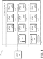
- FIG. 1 is a block diagram of a processing system 100 that includes a processing device 105 according to some embodiments.
- the processing device 105 may be a data processor, a very large scale integrated circuit (VLSI), a system on a chip (SoC), a central processing unit (CPU), an accelerated processing unit (APU), a graphics processing unit (GPU), a memory sub-system, a system controller, a peripheral function, or some other type of processing device.
- the processing device 105 shown in Figure 1 includes a plurality of circuit blocks 111, 112, 113, 114, 115, 116, 117, 118, 119, (referred to herein as "the circuit blocks 111-119”), which may be used to implement portions of the functionality of the processing device 105.
- the circuit blocks 111-119 may therefore be interconnected and communicate with each other, e.g., by transmitting or receiving signals over various lines, traces, buses, vias, through-silicon vias, and the like. In the interest of clarity, interconnections between the circuit blocks 111-119 are not shown in Figure 1 .
- Each circuit block 111-119 is also associated with a power supply monitor (PSM).
- PSM power supply monitor
- Exemplary PSMs are described in U.S. Patent Application Publication No. 2012/0126847 , entitled Power Supply Monitor, by Stephen V. Kosonocky and Gregory K. Chen.
- the PSMs may be incorporated in the circuit blocks 111-119 as shown in Figure 1 or they may be implemented as separate devices that are coupled to the circuit blocks 111-119.
- PSMs may be incorporated in the circuit blocks 111-119 as shown in Figure 1 or they may be implemented as separate devices that are coupled to the circuit blocks 111-119.
- PSMs may be incorporated in the circuit blocks 111-119 as shown in Figure 1 or they may be implemented as separate devices that are coupled to the circuit blocks 111-119.
- PSMs may be associated with more than one circuit block 111-119.
- FIG. 2 is a block diagram of a power supply monitor (PSM) 200 that may be used in the processing device 105 shown in FIG. 1 according to some embodiments.
- PSM power supply monitor
- Some embodiments of the power supply monitor 200 include a ring oscillator 205 that may be formed of multiple stages and the number of stages used to form the ring oscillator 205 may determine, at least in part, the voltage resolution of the power supply monitor 200.
- Techniques for implementing and operating ring oscillators 205 are known in the art and in the interest of clarity only those aspects of implementing or operating the ring oscillator 205 that are relevant to the claimed subject matter are discussed herein.
- a counter 210 in the power supply monitor 200 can count the number of stage transitions in the ring oscillator 205 during a selected measurement period such as a clock cycle, a combination of multiple clock cycles, or a fraction of a clock cycle. For example, voltage droops can slow the oscillator speed of the ring oscillator 205, resulting in fewer stage transitions in the multiple stages of the ring oscillator 205. Increases in the voltage may increase the oscillator speed of the ring oscillator 205 and therefore increase the number of stages traversed in a clock cycle.
- the multiple stages of the ring oscillator 205 are arranged in a ring and so the counter 210 may also count a number of revolutions of the ring oscillator 205 during the measurement period.
- the number of revolutions increases when the voltage increases and decreases during voltage droops.
- Some embodiments of the ring oscillator 205 or the counter 210 may be reset on a leading edge of a clock cycle provided by the clock signal 215.
- Capture logic 220 can capture the state of the ring oscillator at the end of the measurement period.
- the number of stage transitions or ring oscillator revolutions may be indicative of the voltage at the power supply monitor 200.
- Information indicating the number of stage transitions or ring oscillator revolutions counted by the counter 210 (and consequently the voltage measured by the counter 210) during the selected measurement period can be provided to a PSM encoder 225 that supplies a PSM output signal based on the state of the ring oscillator 205 and the number of ring oscillator revolutions at the end of the measurement period.
- Some embodiments of the power supply monitor 200 may provide this information using an interface (not shown).
- the power supply monitor 200 may provide a signal indicating a number of stage transitions of the ring oscillator 205, which is indicative of the voltage measured by the power supply monitor 200, via an interface such as a scan chain that operates according to JTAG protocols.
- the interface may receive capture clock pulses 235 such as the capture clock pulses provided by a scan tester (not shown).
- the relation between the count values returned by the PSM and the PSM voltages may be a function of temperature. Leakage currents for the circuit blocks 111-119 may also depend on temperature.
- Some embodiments of the processing system may therefore include temperature sensor logic (TCEN) 120 that can be used to determine temperatures on the processing device 105.
- the TCEN 120 may include or be coupled to a temperature sensor 125 for monitoring temperatures.
- the temperature sensor 125 may be a single sensor or may be representative of a plurality of sensors distributed throughout the processing device 105.
- the processing system 100 also includes a power supply 130 that can be coupled to the processing device 105 to provide power to the circuit blocks 111-119 at a nominal voltage.
- the processing device 105 may be coupled to different power supplies 130 during different stages.
- the power supply 130 may be an ATE power supply 130 during ATE testing of the processing device 105, an SLT power supply 130 during system-level testing of the processing device 105, and a consumer device power supply 130 after the processing device 105 has been installed in a consumer product.
- the characteristics of the different power supplies 130 may be significantly different.
- an ATE power supply 130 is typically a very high-quality power supply 130 that may experience substantially no voltage droop (or a voltage droop that is within a very low tolerance such as a few mV for a 1.3V applied voltage) during testing of the processing device 105.
- an SLT power supply 130 or a consumer product power supply 130 may experience significantly higher voltage droops, e.g., a voltage droop of 0.05V to 0.1V for a 1.3V applied voltage under high operating loads that may occur during testing of the processing device 105.
- the characteristics of different consumer product power supplies 130 may differ from each other and may change over time as the power supply 130 ages.
- the processing device 105 may therefore include calibration logic 135 that can determine voltages supplied to the circuit blocks 111-119 and use these voltages to generate a calibration signal for controlling the voltage provided by the power supply 130.
- the voltages in the circuit blocks 111-119 may not be equal to the voltage generated by the power supply 130, e.g. due to voltage droop.
- Each PSM may therefore measure voltages at the location of the PSM and the measured voltages may be indicative of the voltage that is applied to the corresponding circuit block 111-119.
- the calibration logic 135 may access the measured voltages from the PSMs and compare the measured voltages to a reference voltage, which may be stored in a storage element 140 that may be formed of registers or fuses. For example, the calibration logic 135 may compare an average of the voltages measured by the PSMs or a minimum voltage from among the voltages measured by the PSMs to the reference voltage and then provide an adjustment signal to the power supply 130, as discussed herein.
- the reference voltage may be determined during testing of the processing device 105.
- the processing device 105 is tested by executing a series of code loops that are defined by a testing algorithm, which may be implemented by the calibration logic 135.
- the code loops may be executed while the processing device 105 is coupled to an ATE power supply 130.
- the calibration logic 135 reads values from the PSMs concurrently with executing the code loops and then determines the reference voltage based on the measured values of the PSM voltages.
- Some embodiments of the calibration logic 135 may use statistical combinations of the PSM voltages such as means of the PSM voltages, a median of the PSM voltages, a mode of the PSM voltages, a minimum of the PSM voltages, a maximum of the PSM voltages, and the like. Subsequently, the processing device 105 may be coupled to other power supplies 130 and the same testing algorithm may be executed to calibrate the other power supplies 130 by comparison to the reference voltage, as discussed herein.
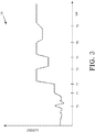
- FIG. 3 is a plot 300 of current drawn from a power supply as a function of time during execution of code loops defined by a testing algorithm according to some embodiments.
- the vertical axis indicates the current (in arbitrary units) and the horizontal axis indicates the time (in arbitrary units) increasing from left to right.
- Some embodiments of the plot 300 may correspond to current drawn by the processing device 105 while executing code loops defined by a testing algorithm implemented in the calibration logic 135 shown in FIG. 1 . The same testing algorithm may be executed by the calibration logic 135 each time the processing device 105 boots up.
- Some embodiments of the testing algorithm illustrated in the plot 300 may be designed to test AC response, DC response, or resonant frequencies of processing device 105.
- the processing device is in a quiescent or inactive state and the current corresponds to leakage currents in the processing device.
- a system BIOS initiates a system management unit (SMU) routine to begin testing of the processing device.
- SMU system management unit
- the processing device executes a first base power code loop.
- the voltage at locations in the processing device may settle or stabilize over this time interval. Voltage measurements may therefore be performed by PSMs during this time interval and concurrently with execution of the first base power code loop.
- a step load is applied to the processing device to increase the supply of power to a maximum level that can be provided by the power supply.
- Voltage measurements may be performed by PSMs during this time interval concurrently with execution of the code that creates the step load.
- the processing device executes a second base power code loop.
- the operating load corresponding to the second base power code loop is larger than the operating load corresponding to the first base power code loop, as indicated by the higher values of the current.
- the voltage at locations in the processing device may settle or stabilize over this time interval. Voltage measurements may be performed by PSMs concurrently with execution of the second base power code loop.
- a step load is applied to the processing device to increase the supply of power to the maximum level that can be provided by the power supply.
- Voltage measurements may be performed by PSMs concurrently with execution of the code used to generate the step load.
- the processing device executes a third base power code loop.
- the operating load corresponding to the third base power code loop is larger than the operating load corresponding to the second base power code loop, as indicated by the higher values of the current.
- the voltage at locations in the processing device may settle or stabilize over this time interval. Voltage measurements may be performed by PSMs concurrently with execution of the third base power code loop.
- a step load is applied to the processing device to increase the supply of power to the maximum level that can be provided by the power supply.
- the current therefore rises to a maximum value and stays at this level until the testing algorithm completes.
- Final voltage measurements may be performed by PSMs after a time interval sufficient to allow the voltages to stabilize and concurrently with execution of the code that generates the step load.
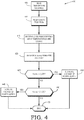
- FIG. 4 is a flow diagram of a method 400 for calibrating a power supply that provides power to a processing device according to some embodiments.
- the method 400 may be implemented in calibration logic such as the calibration logic 135 shown in FIG. 1 and may be initiated in response to boot up of a processing device such as the processing device 105 shown in FIG. 1 .
- the calibration logic reads temperatures provided by one or more temperature sensors or temperature sensing logic such as the TCEN 120 shown in FIG. 1 . Some embodiments of the calibration logic read the temperatures as an initial step so that the temperature can be determined before it decreases due to inactivity.
- the calibration logic reads counts from the PSMs in the processing device.
- Some embodiments of the PSMs may be sensitive to temperature.
- the counts may therefore be converted (at block 415) to voltages based on the temperature that was read by the calibration logic at block 405.
- the temperature value may be compared to a reference temperature and the difference may be used to scale the measured counts from the PSMs, e.g., by increasing or decreasing the measured counts in proportion to the difference between the measured temperature value and the reference temperature.
- the scaled counts may then be used to determine the voltage at the PSM.
- the tests performed at block 405, 410, 415 may be iterated to measure voltages at different stages in the testing algorithm, e.g ., as illustrated in FIG. 3 .
- the calibration logic determines a comparison voltage (Vcomp) based on the voltages measured by the PSMs.
- Vcomp a comparison voltage
- Some embodiments of the calibration logic may determine the comparison voltage using a minimum-of-minimums of the voltages measured by the PSMs during execution of the testing algorithm.
- the calibration logic may also determine the comparison voltage using other statistical combinations of the measured voltages such as means, medians, modes, maximums, and the like.
- the calibration logic compares the comparison voltage to a reference voltage such as a voltage (V_ATE) determined during ATE testing.
- a reference voltage such as a voltage (V_ATE) determined during ATE testing.
- V_ATE a voltage
- the reference voltage and the comparison voltage are determined using the same testing algorithm and the same statistical combination of the measured voltages. If the comparison voltage is larger than the reference voltage, then the calibration logic may generate (at block 430) a signal instructing the power supply to decrease its supply voltage. The method 400 may then end at block 435. If the comparison voltage is smaller than the reference voltage (as determined at decision block 440), the calibration logic may generate (at block 445) a signal instructing the power supply to increase its supply voltage. The method 400 may then end at block 435.
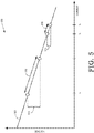
- FIG. 5 is a plot 500 of a load line 505 that may be used to adjust the voltage provided by a power supply to compensate for leakage current according to some embodiments.
- the vertical axis is a voltage (in arbitrary units) provided by a power supply and the horizontal axis is a leakage current (in arbitrary units) at the corresponding voltage.
- Leakage currents typically increase with increasing temperature and FIG. 5 shows the voltage adjustments that may be used to compensate for leakage currents at different temperatures in two processing devices that have different sensitivities to temperature. For example, at low temperatures the leakage current of the first processing device may be a relatively low current (I 0 ) and may increase to a relatively high current (I 1 ) at higher temperatures.
- the power supply voltage may therefore be varied along the load line (as indicated by the arrow 510) to compensate for the variations in the leakage current.
- the power supply voltage may vary within the range 515 for the first processing device.
- the leakage current of the second processing device may be a relatively low current (I 2 ) and may increase to a relatively high current (I 3 ) at higher temperatures, although the variation in leakage currents is smaller than for the first processing device.
- the power supply voltage may therefore be varied along the load line (as indicated by the arrow 520) to compensate for the variations in the leakage current.
- the power supply voltage may therefore vary within the range 525 for the second processing device.
- the calibration logic used for boot time calibration should account for variations in the voltage provided by the power supply that are generated by the load line or other voltage compensation mechanisms. For example, if logic associated with the load line instructs the power supply to increase or decrease its voltage to compensate for leakage currents, the calibration logic should account for this modification so that the actual voltage provided by the power supply after incorporating modifications from the load line logic and the calibration logic corresponds to the reference voltage, at least within a predetermined tolerance. For example, the calibration logic may add or subtract a load line voltage adjustment from the comparison voltage determined at boot time to avoid an over-voltage condition.
- FIG. 6 is a flow diagram of a method 600 for calibrating a power supply to account for other voltage modifications according to some embodiments.
- the method 600 may be implemented in calibration logic such as the calibration logic 135 shown in FIG. 1 and may be initiated in response to boot up of a processing device such as the processing device 105 shown in FIG. 1 .
- the calibration logic reads temperatures provided by one or more temperature sensors or temperature sensing logic such as the TCEN 120 shown in FIG. 1 .
- the calibration logic reads counts from the PSMs in the processing device. As discussed herein, blocks 605 or 610 may be iterated to gather voltage measurements concurrently with execution of multiple code loops according to a testing algorithm.
- the calibration logic determines a voltage offset. For example, the voltage offset may be set equal to the difference between the previously determined reference voltage and a comparison voltage determined based on the measured voltages.
- the calibration logic may determine other voltage modifications. For example, the calibration logic may access information indicating voltage compensations determined using a load line such as the load line 505 shown in FIG. 5 .
- the voltage compensation determined by the load line may depend on the temperature of the processing device and the calibration logic may therefore use the temperatures provided by temperature sensing logic to determine the voltage compensation.
- Some embodiments may apply other voltage compensations. For example, a fixed voltage offset may be applied to account for an expected difference between the voltages provided by a first power supply (such as an ATE power supply) and a second power supply (such as an SLT or consumer product power supply).
- the calibration logic may adjust the voltage offset based on the other voltage compensations.
- the calibration logic may adjust the voltage offset so that the net change to the voltage provided by the power supply is equal to a difference between the reference voltage and the comparison voltage determined based on the PSM measurements.
- the voltage offset may be applied to the power supply to modify the voltage provided by the power supply.
- FIG. 7 is a block diagram 700 illustrating operation of calibration logic 705 in an SOC 710 in different operational contexts according to some embodiments.
- Some embodiments of the calibration logic 705 may correspond to the calibration logic 135 in the processing device 105 shown in FIG. 1 .
- the SOC 710 is initially placed into an ATE 715 for testing.
- the SOC 710 is coupled to an ATE power supply 720 and then the calibration logic 705 may initiate a test algorithm that causes the SOC 710 to execute one or more code loops that place different operating loads on the SOC 710.
- the calibration logic 705 may determine a reference voltage using one or more PSM voltage measurements performed concurrently with execution of the code loops.
- the reference voltage may then be associated with the SOC 710 and stored.
- Some embodiments may store the reference voltage in a database 725 that lists the reference voltage is for each part that is tested in the ATE 715.
- the database 725 may be accessed by other testing devices or other software, firmware, or hardware for other purposes.
- the SOC 710 may subsequently be moved to an SLT environment for system-level testing.
- the SOC 710 is coupled to an SLT power supply 735 and then the calibration logic 705 may initiate the test algorithm that causes the SOC 710 to execute one or more code loops that place different operating loads on the SOC 710.
- the test algorithm used by the SOC 710 in the SLT 730 is the same as the test algorithm used by the SOC 710 in the ATE 715.
- the calibration logic 705 may determine a comparison voltage using one or more PSM voltage measurements performed concurrently with execution of the code loops. The calibration logic 705 may then compare the comparison voltage to the reference voltage, e.g., the reference voltage stored in the database 725.
- the calibration logic 705 may then provide a calibration signal to the SLT power supply 735 to adjust the voltage provided to the SOC 710 by the SLT power supply 735, as discussed herein.
- the adjusted voltage may then be provided to the SOC 710 during subsequent performance testing.
- the SOC 710 may subsequently be installed in a consumer product or device 740.
- the installed SOC 710 is coupled to a device power supply 745.
- the reference voltage is stored in a storage element 750 such as a set of registers or fuses that can be configured using the information stored in the database 725.
- the calibration logic 705 may then initiate the test algorithm each time the device 740 is booted up so that the SOC 710 executes the code loops defined by the testing algorithm at boot time.
- the test algorithm used by the SOC 710 in the device 740 is the same as the test algorithm used by the SOC 710 in the ATE 715 and the SLT 730.
- the calibration logic 705 may determine a comparison voltage using one or more PSM voltage measurements performed concurrently with execution of the code loops. The calibration logic 705 may then compare the comparison voltage to the reference voltage, e.g., the reference voltage stored in the storage element 750. Based on the comparison, the calibration logic 705 may provide a calibration signal to the device power supply 745 to adjust the voltage provided to the SOC 710 by the device power supply 745, as discussed herein. The adjusted voltage may then be provided to the SOC 710 during normal operation of the device 740.
- the reference voltage e.g., the reference voltage stored in the storage element 750. Based on the comparison, the calibration logic 705 may provide a calibration signal to the device power supply 745 to adjust the voltage provided to the SOC 710 by the device power supply 745, as discussed herein. The adjusted voltage may then be provided to the SOC 710 during normal operation of the device 740.
- FIG. 8 is a flow diagram of a method 800 for creating a reference voltage using a first power supply and then modifying a voltage provided by a second power supply based on the reference voltage according to some embodiments.
- the method 800 may be implemented in calibration logic of a processing device such as the calibration logic 135 of the processing device 105 shown in FIG. 1 .
- the calibration logic determines a reference voltage while the processing device is coupled to a first power supply.
- the reference voltage is determined using voltage measurements performed concurrently with executing a predetermined testing algorithm, as discussed herein.
- the reference voltage is stored, e.g., in a database, a set of registers, or a set of fuses.
- the processing device may then be disconnected from the first power supply and connected to a second power supply.
- the calibration logic determines a comparison voltage using voltage measurements performed concurrently with executing the predetermined testing algorithm, as discussed herein.
- the calibration logic determines whether the comparison voltage is different than the reference voltage. If so, the calibration logic modifies (at block 825) the voltage provided by the second power supply based on an offset between the comparison voltage and the reference voltage, as discussed herein. The method may then end at block 830. If the comparison voltage is not different than the reference voltage, e.g., the difference between the comparison voltage and the reference voltage is less than a predetermined tolerance, the calibration logic bypasses modifying the voltage provided by the second power supply and the method may end at block 830.
- the apparatus and techniques described above are implemented in a system comprising one or more integrated circuit (IC) devices (also referred to as integrated circuit packages or microchips), such as the processing device described above with reference to FIGs. 1-8 .
- IC integrated circuit
- EDA electronic design automation
- CAD computer aided design
- These design tools typically are represented as one or more software programs.
- the one or more software programs comprise code executable by a computer system to manipulate the computer system to operate on code representative of circuitry of one or more IC devices so as to perform at least a portion of a process to design or adapt a manufacturing system to fabricate the circuitry.
- This code can include instructions, data, or a combination of instructions and data.
- the software instructions representing a design tool or fabrication tool typically are stored in a computer readable storage medium accessible to the computing system.
- the code representative of one or more phases of the design or fabrication of an IC device may be stored in and accessed from the same computer readable storage medium or a different computer readable storage medium.
- a computer readable storage medium may include any storage medium, or combination of storage media, accessible by a computer system during use to provide instructions and/or data to the computer system.
- Such storage media can include, but is not limited to, optical media (e.g., compact disc (CD), digital versatile disc (DVD), Blu-Ray disc), magnetic media (e.g., floppy disc, magnetic tape, or magnetic hard drive), volatile memory (e.g., random access memory (RAM) or cache), non-volatile memory (e.g., read-only memory (ROM) or Flash memory), or microelectromechanical systems (MEMS)-based storage media.
- optical media e.g., compact disc (CD), digital versatile disc (DVD), Blu-Ray disc
- magnetic media e.g., floppy disc, magnetic tape, or magnetic hard drive
- volatile memory e.g., random access memory (RAM) or cache
- non-volatile memory e.g., read-only memory (ROM) or Flash memory
- MEMS microelectro
- the computer readable storage medium may be embedded in the computing system (e.g., system RAM or ROM), fixedly attached to the computing system (e.g., a magnetic hard drive), removably attached to the computing system (e.g., an optical disc or Universal Serial Bus (USB)-based Flash memory), or coupled to the computer system via a wired or wireless network (e.g., network accessible storage (NAS)).
- system RAM or ROM system RAM or ROM
- USB Universal Serial Bus
- NAS network accessible storage
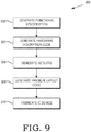
- FIG. 9 is a flow diagram illustrating an example method 900 for the design and fabrication of an IC device implementing one or more aspects in accordance with some embodiments.
- the code generated for each of the following processes is stored or otherwise embodied in non-transitory computer readable storage media for access and use by the corresponding design tool or fabrication tool.
- a functional specification for the IC device is generated.
- the functional specification (often referred to as a micro architecture specification (MAS)) may be represented by any of a variety of programming languages or modeling languages, including C, C++, SystemC, Simulink, or MATLAB.
- the functional specification is used to generate hardware description code representative of the hardware of the IC device.
- the hardware description code is represented using at least one Hardware Description Language (HDL), which comprises any of a variety of computer languages, specification languages, or modeling languages for the formal description and design of the circuits of the IC device.
- HDL Hardware Description Language
- the generated HDL code typically represents the operation of the circuits of the IC device, the design and organization of the circuits, and tests to verify correct operation of the IC device through simulation. Examples of HDL include Analog HDL (AHDL), Verilog HDL, SystemVerilog HDL, and VHDL.
- the hardware descriptor code may include register transfer level (RTL) code to provide an abstract representation of the operations of the synchronous digital circuits.
- RTL register transfer level
- the hardware descriptor code may include behavior-level code to provide an abstract representation of the circuitry's operation.
- the HDL model represented by the hardware description code typically is subjected to one or more rounds of simulation and debugging to pass design verification.
- a synthesis tool is used to synthesize the hardware description code to generate code representing or defining an initial physical implementation of the circuitry of the IC device.
- the synthesis tool generates one or more netlists comprising circuit device instances (e.g., gates, transistors, resistors, capacitors, inductors, diodes, etc.) and the nets, or connections, between the circuit device instances.
- circuit device instances e.g., gates, transistors, resistors, capacitors, inductors, diodes, etc.
- all or a portion of a netlist can be generated manually without the use of a synthesis tool.
- the netlists may be subjected to one or more test and verification processes before a final set of one or more netlists is generated.
- a schematic editor tool can be used to draft a schematic of circuitry of the IC device and a schematic capture tool then may be used to capture the resulting circuit diagram and to generate one or more netlists (stored on a computer readable media) representing the components and connectivity of the circuit diagram.
- the captured circuit diagram may then be subjected to one or more rounds of simulation for testing and verification.
- one or more EDA tools use the netlists produced at block 906 to generate code representing the physical layout of the circuitry of the IC device.
- This process can include, for example, a placement tool using the netlists to determine or fix the location of each element of the circuitry of the IC device. Further, a routing tool builds on the placement process to add and route the wires needed to connect the circuit elements in accordance with the netlist(s).
- the resulting code represents a three-dimensional model of the IC device.
- the code may be represented in a database file format, such as, for example, the Graphic Database System II (GDSII) format. Data in this format typically represents geometric shapes, text labels, and other information about the circuit layout in hierarchical form.
- GDSII Graphic Database System II
- the physical layout code (e.g., GDSII code) is provided to a manufacturing facility, which uses the physical layout code to configure or otherwise adapt fabrication tools of the manufacturing facility (e.g., through mask works) to fabricate the IC device. That is, the physical layout code may be programmed into one or more computer systems, which may then control, in whole or part, the operation of the tools of the manufacturing facility or the manufacturing operations performed therein.
- certain aspects of the techniques described above may implemented by one or more processors of a processing system executing software.
- the software comprises one or more sets of executable instructions stored or otherwise tangibly embodied on a non-transitory computer readable storage medium.
- the software can include the instructions and certain data that, when executed by the one or more processors, manipulate the one or more processors to perform one or more aspects of the techniques described above.
- the non-transitory computer readable storage medium can include, for example, a magnetic or optical disk storage device, solid state storage devices such as Flash memory, a cache, random access memory (RAM) or other non-volatile memory device or devices, and the like.
- the executable instructions stored on the non-transitory computer readable storage medium may be in source code, assembly language code, object code, or other instruction format that is interpreted or otherwise executable by one or more processors.
Landscapes
- Engineering & Computer Science (AREA)
- Theoretical Computer Science (AREA)
- Physics & Mathematics (AREA)
- General Physics & Mathematics (AREA)
- General Engineering & Computer Science (AREA)
- Power Sources (AREA)
- Power Engineering (AREA)
- Tests Of Electronic Circuits (AREA)
- Test And Diagnosis Of Digital Computers (AREA)
Description
- The present disclosure relates generally to processing systems and, more particularly, to supplying power to processing systems.
- Automatic test equipment (ATE) is used to test processing systems such as a system-on-a-chip (SOC) after fabrication and prior to installation in a product. For example, automated testing may be used to determine the operating frequencies of components of the SOC under different operating loads for a given applied voltage. A typical ATE includes a very high-quality voltage supply that can maintain a constant applied voltage within a very narrow tolerance for a wide range of operating loads. However, the system-level voltage supplies that are used in products such as desktop computers, laptop computers, tablets, smart phones, and the like are not able to maintain the same voltage tolerances over the same range of operating loads. For example, if the load on an SOC suddenly increases from a very low level to a relatively high level, the current drawn by the components of the SOC increases and the voltage provided to components of the SOC falls, a phenomenon known as "voltage droop." The operating frequencies of the components of the SOC also fall when the voltage droops.
- The amount of voltage droop depends on the characteristics of the power supply and the load on the SOC. Virtually every product that is shipped to a consumer has a slightly different power supply and will experience different operating loads over its lifetime. Thus, the power supply characteristics and the operating loads of each consumer product are not precisely known and may change over the lifetime of the product. Consequently, an SOC that is rated for a particular operating frequency must include a voltage margin to ensure that the actual operating frequency of the SOC does not fall below the rated value during voltage droop. The voltage margin is typically set by assuming a worst-case scenario, e.g., the largest expected voltage droop under the highest operating loads. During normal operation, e.g., under moderate or light operating loads, the voltage margin is unnecessary and may therefore represent wasted power or an operating frequency in excess of the rated value.
-
US 7772811 B1 andUS 2005/218871 A1 show adaptive voltages provided to a processing system. -
US 2012/218034 A1 shows a calibration of a power supply. - The present disclosure may be better understood, and its numerous features and advantages made apparent to those skilled in the art by referencing the accompanying drawings. The use of the same reference symbols in different drawings indicates similar or identical items.
-
FIG. 1 is a block diagram of a processing system that includes a processing device according to some embodiments. -
FIG. 2 is a block diagram of a power supply monitor (PSM) that may be used in the processing device shown inFIG. 1 according to some embodiments. -
FIG. 3 is a plot of current drawn from a power supply as a function of time during execution of code loops defined by testing algorithm according to some embodiments. -
FIG. 4 is a flow diagram of a method for calibrating a power supply that provides power to a processing device according to some embodiments. -
FIG. 5 is a plot of a load line that may be used to adjust the voltage provided by a power supply to compensate for leakage current according to some embodiments. -
FIG. 6 is a flow diagram of a method for calibrating a power supply to account for other voltage modifications according to some embodiments. -
FIG. 7 is a block diagram illustrating operation of calibration logic in an SOC in different operational contexts according to some embodiments. -
FIG. 8 is a flow diagram of a method for creating a reference voltage using a first power supply and then modifying a voltage provided by a second power supply based on the reference voltage according to some embodiments. -
FIG. 9 is a flow diagram illustrating a method for designing and fabricating an integrated circuit device implementing at least a portion of a component of a processing system in accordance with some embodiments. - The invention is defined by the appended independent claims. Further aspects of the invention are outlined in the dependent claims. Embodiments which do not fall within the scope of the claims do not form part of the present invention.
- The voltage margins used to account for possible voltage droop in a processing system can be reduced by calibrating the voltage provided to the processing system at boot time based on a comparison of a previously determined reference voltage and measurements of voltages at different locations in the processing system. The reference voltage is determined based on a testing algorithm and the boot time voltage measurements are performed while executing the same testing algorithm. In some embodiments, the processing system is connected to a first power supply in automated test equipment (ATE) and executes a series of code loops that are defined by the testing algorithm. The reference voltage is then determined based on measurements taken by power supply monitors (PSMs) implemented in the processing system. Subsequently, the processing system executes the same series of code loops while connected to a second power supply, such as a power supply in a system-level test (SLT) environment or a power supply in a user product. Voltages are measured by the PSMs concurrently with executing the code loops. The measured voltages are then compared to the reference voltage to determine a voltage offset that should be applied to the power supply implemented in the processing system. For example, the voltage offset may be used to increase the voltage provided by the power supply if an average value of the voltages measured by the PSMs during execution of the code loops is below the reference voltage. For another example, the voltage offset may be used to decrease the voltage provided by the power supply if the average value of the voltages measured by the PSMs during execution of the code loops is higher than the reference voltage. The SOC may therefore dynamically control its power supply to keep the power supply operating at a voltage that ensures that the voltage received at locations within the SOC are near a target voltage.
-
FIG. 1 is a block diagram of aprocessing system 100 that includes aprocessing device 105 according to some embodiments. Theprocessing device 105 may be a data processor, a very large scale integrated circuit (VLSI), a system on a chip (SoC), a central processing unit (CPU), an accelerated processing unit (APU), a graphics processing unit (GPU), a memory sub-system, a system controller, a peripheral function, or some other type of processing device. Theprocessing device 105 shown inFigure 1 includes a plurality ofcircuit blocks processing device 105. The circuit blocks 111-119 may therefore be interconnected and communicate with each other, e.g., by transmitting or receiving signals over various lines, traces, buses, vias, through-silicon vias, and the like. In the interest of clarity, interconnections between the circuit blocks 111-119 are not shown inFigure 1 . - Each circuit block 111-119 is also associated with a power supply monitor (PSM). Exemplary PSMs are described in
U.S. Patent Application Publication No. 2012/0126847 , entitled Power Supply Monitor, by Stephen V. Kosonocky and Gregory K. Chen. The PSMs may be incorporated in the circuit blocks 111-119 as shown inFigure 1 or they may be implemented as separate devices that are coupled to the circuit blocks 111-119. However, persons of ordinary skill in the art having benefit of the present disclosure should appreciate that some embodiments of theprocessing device 105 may include circuit blocks 111-119 that are associated with more than one PSM. Moreover, some PSMs may be associated with more than one circuit block 111-119. -
FIG. 2 is a block diagram of a power supply monitor (PSM) 200 that may be used in theprocessing device 105 shown inFIG. 1 according to some embodiments. Some embodiments of thepower supply monitor 200 include aring oscillator 205 that may be formed of multiple stages and the number of stages used to form thering oscillator 205 may determine, at least in part, the voltage resolution of thepower supply monitor 200. Techniques for implementing and operatingring oscillators 205 are known in the art and in the interest of clarity only those aspects of implementing or operating thering oscillator 205 that are relevant to the claimed subject matter are discussed herein. - A
counter 210 in thepower supply monitor 200 can count the number of stage transitions in thering oscillator 205 during a selected measurement period such as a clock cycle, a combination of multiple clock cycles, or a fraction of a clock cycle. For example, voltage droops can slow the oscillator speed of thering oscillator 205, resulting in fewer stage transitions in the multiple stages of thering oscillator 205. Increases in the voltage may increase the oscillator speed of thering oscillator 205 and therefore increase the number of stages traversed in a clock cycle. The multiple stages of thering oscillator 205 are arranged in a ring and so thecounter 210 may also count a number of revolutions of thering oscillator 205 during the measurement period. The number of revolutions increases when the voltage increases and decreases during voltage droops. Some embodiments of thering oscillator 205 or thecounter 210 may be reset on a leading edge of a clock cycle provided by theclock signal 215.Capture logic 220 can capture the state of the ring oscillator at the end of the measurement period. - The number of stage transitions or ring oscillator revolutions may be indicative of the voltage at the
power supply monitor 200. Information indicating the number of stage transitions or ring oscillator revolutions counted by the counter 210 (and consequently the voltage measured by the counter 210) during the selected measurement period can be provided to aPSM encoder 225 that supplies a PSM output signal based on the state of thering oscillator 205 and the number of ring oscillator revolutions at the end of the measurement period. Some embodiments of thepower supply monitor 200 may provide this information using an interface (not shown). For example, thepower supply monitor 200 may provide a signal indicating a number of stage transitions of thering oscillator 205, which is indicative of the voltage measured by thepower supply monitor 200, via an interface such as a scan chain that operates according to JTAG protocols. The interface may receive capture clock pulses 235 such as the capture clock pulses provided by a scan tester (not shown). - Referring back to
FIG. 1 , the relation between the count values returned by the PSM and the PSM voltages may be a function of temperature. Leakage currents for the circuit blocks 111-119 may also depend on temperature. Some embodiments of the processing system may therefore include temperature sensor logic (TCEN) 120 that can be used to determine temperatures on theprocessing device 105. For example, theTCEN 120 may include or be coupled to atemperature sensor 125 for monitoring temperatures. Thetemperature sensor 125 may be a single sensor or may be representative of a plurality of sensors distributed throughout theprocessing device 105. - The
processing system 100 also includes apower supply 130 that can be coupled to theprocessing device 105 to provide power to the circuit blocks 111-119 at a nominal voltage. Theprocessing device 105 may be coupled todifferent power supplies 130 during different stages. For example, thepower supply 130 may be an ATEpower supply 130 during ATE testing of theprocessing device 105, anSLT power supply 130 during system-level testing of theprocessing device 105, and a consumerdevice power supply 130 after theprocessing device 105 has been installed in a consumer product. The characteristics of thedifferent power supplies 130 may be significantly different. For example, an ATEpower supply 130 is typically a very high-quality power supply 130 that may experience substantially no voltage droop (or a voltage droop that is within a very low tolerance such as a few mV for a 1.3V applied voltage) during testing of theprocessing device 105. For another example, anSLT power supply 130 or a consumerproduct power supply 130 may experience significantly higher voltage droops, e.g., a voltage droop of 0.05V to 0.1V for a 1.3V applied voltage under high operating loads that may occur during testing of theprocessing device 105. The characteristics of different consumerproduct power supplies 130 may differ from each other and may change over time as thepower supply 130 ages. - The
processing device 105 may therefore includecalibration logic 135 that can determine voltages supplied to the circuit blocks 111-119 and use these voltages to generate a calibration signal for controlling the voltage provided by thepower supply 130. For example, as discussed herein, the voltages in the circuit blocks 111-119 may not be equal to the voltage generated by thepower supply 130, e.g. due to voltage droop. Each PSM may therefore measure voltages at the location of the PSM and the measured voltages may be indicative of the voltage that is applied to the corresponding circuit block 111-119. Thecalibration logic 135 may access the measured voltages from the PSMs and compare the measured voltages to a reference voltage, which may be stored in astorage element 140 that may be formed of registers or fuses. For example, thecalibration logic 135 may compare an average of the voltages measured by the PSMs or a minimum voltage from among the voltages measured by the PSMs to the reference voltage and then provide an adjustment signal to thepower supply 130, as discussed herein. - The reference voltage may be determined during testing of the
processing device 105. In some embodiments, theprocessing device 105 is tested by executing a series of code loops that are defined by a testing algorithm, which may be implemented by thecalibration logic 135. The code loops may be executed while theprocessing device 105 is coupled to an ATEpower supply 130. Thecalibration logic 135 reads values from the PSMs concurrently with executing the code loops and then determines the reference voltage based on the measured values of the PSM voltages. Some embodiments of thecalibration logic 135 may use statistical combinations of the PSM voltages such as means of the PSM voltages, a median of the PSM voltages, a mode of the PSM voltages, a minimum of the PSM voltages, a maximum of the PSM voltages, and the like. Subsequently, theprocessing device 105 may be coupled toother power supplies 130 and the same testing algorithm may be executed to calibrate theother power supplies 130 by comparison to the reference voltage, as discussed herein. -
FIG. 3 is aplot 300 of current drawn from a power supply as a function of time during execution of code loops defined by a testing algorithm according to some embodiments. The vertical axis indicates the current (in arbitrary units) and the horizontal axis indicates the time (in arbitrary units) increasing from left to right. Some embodiments of theplot 300 may correspond to current drawn by theprocessing device 105 while executing code loops defined by a testing algorithm implemented in thecalibration logic 135 shown inFIG. 1 . The same testing algorithm may be executed by thecalibration logic 135 each time theprocessing device 105 boots up. Some embodiments of the testing algorithm illustrated in theplot 300 may be designed to test AC response, DC response, or resonant frequencies ofprocessing device 105. - At T<T0, the processing device is in a quiescent or inactive state and the current corresponds to leakage currents in the processing device.
- At T = T0, a system BIOS initiates a system management unit (SMU) routine to begin testing of the processing device.
- At T1 < T < T2, the processing device executes a first base power code loop. The voltage at locations in the processing device may settle or stabilize over this time interval. Voltage measurements may therefore be performed by PSMs during this time interval and concurrently with execution of the first base power code loop.
- At T = T2, a step load is applied to the processing device to increase the supply of power to a maximum level that can be provided by the power supply. The current therefore rises to a maximum value and stays at this level until T = T3. Voltage measurements may be performed by PSMs during this time interval concurrently with execution of the code that creates the step load.
- At T3 < T < T4, the processing device executes a second base power code loop. The operating load corresponding to the second base power code loop is larger than the operating load corresponding to the first base power code loop, as indicated by the higher values of the current. The voltage at locations in the processing device may settle or stabilize over this time interval. Voltage measurements may be performed by PSMs concurrently with execution of the second base power code loop.
- At T = T4, a step load is applied to the processing device to increase the supply of power to the maximum level that can be provided by the power supply. The current therefore rises to a maximum value and stays at this level until T = T5. Voltage measurements may be performed by PSMs concurrently with execution of the code used to generate the step load.
- At T5 < T < T6, the processing device executes a third base power code loop. The operating load corresponding to the third base power code loop is larger than the operating load corresponding to the second base power code loop, as indicated by the higher values of the current. The voltage at locations in the processing device may settle or stabilize over this time interval. Voltage measurements may be performed by PSMs concurrently with execution of the third base power code loop.
- At T = T6, a step load is applied to the processing device to increase the supply of power to the maximum level that can be provided by the power supply. The current therefore rises to a maximum value and stays at this level until the testing algorithm completes. Final voltage measurements may be performed by PSMs after a time interval sufficient to allow the voltages to stabilize and concurrently with execution of the code that generates the step load.
-
FIG. 4 is a flow diagram of amethod 400 for calibrating a power supply that provides power to a processing device according to some embodiments. Themethod 400 may be implemented in calibration logic such as thecalibration logic 135 shown inFIG. 1 and may be initiated in response to boot up of a processing device such as theprocessing device 105 shown inFIG. 1 . Atblock 405, the calibration logic reads temperatures provided by one or more temperature sensors or temperature sensing logic such as theTCEN 120 shown inFIG. 1 . Some embodiments of the calibration logic read the temperatures as an initial step so that the temperature can be determined before it decreases due to inactivity. - At
block 410, the calibration logic reads counts from the PSMs in the processing device. Some embodiments of the PSMs may be sensitive to temperature. The counts may therefore be converted (at block 415) to voltages based on the temperature that was read by the calibration logic atblock 405. For example, the temperature value may be compared to a reference temperature and the difference may be used to scale the measured counts from the PSMs, e.g., by increasing or decreasing the measured counts in proportion to the difference between the measured temperature value and the reference temperature. The scaled counts may then be used to determine the voltage at the PSM. The tests performed atblock FIG. 3 . - At
block 420, the calibration logic determines a comparison voltage (Vcomp) based on the voltages measured by the PSMs. Some embodiments of the calibration logic may determine the comparison voltage using a minimum-of-minimums of the voltages measured by the PSMs during execution of the testing algorithm. However, the calibration logic may also determine the comparison voltage using other statistical combinations of the measured voltages such as means, medians, modes, maximums, and the like. - At
decision block 425, the calibration logic compares the comparison voltage to a reference voltage such as a voltage (V_ATE) determined during ATE testing. As discussed herein, the reference voltage and the comparison voltage are determined using the same testing algorithm and the same statistical combination of the measured voltages. If the comparison voltage is larger than the reference voltage, then the calibration logic may generate (at block 430) a signal instructing the power supply to decrease its supply voltage. Themethod 400 may then end atblock 435. If the comparison voltage is smaller than the reference voltage (as determined at decision block 440), the calibration logic may generate (at block 445) a signal instructing the power supply to increase its supply voltage. Themethod 400 may then end atblock 435. -
FIG. 5 is a plot 500 of a load line 505 that may be used to adjust the voltage provided by a power supply to compensate for leakage current according to some embodiments. The vertical axis is a voltage (in arbitrary units) provided by a power supply and the horizontal axis is a leakage current (in arbitrary units) at the corresponding voltage. Leakage currents typically increase with increasing temperature andFIG. 5 shows the voltage adjustments that may be used to compensate for leakage currents at different temperatures in two processing devices that have different sensitivities to temperature. For example, at low temperatures the leakage current of the first processing device may be a relatively low current (I0) and may increase to a relatively high current (I1) at higher temperatures. The power supply voltage may therefore be varied along the load line (as indicated by the arrow 510) to compensate for the variations in the leakage current. The power supply voltage may vary within the range 515 for the first processing device. For another example, at low temperatures the leakage current of the second processing device may be a relatively low current (I2) and may increase to a relatively high current (I3) at higher temperatures, although the variation in leakage currents is smaller than for the first processing device. The power supply voltage may therefore be varied along the load line (as indicated by the arrow 520) to compensate for the variations in the leakage current. The power supply voltage may therefore vary within the range 525 for the second processing device. - The calibration logic used for boot time calibration (such as the
calibration logic 135 shown inFIG. 1 ) should account for variations in the voltage provided by the power supply that are generated by the load line or other voltage compensation mechanisms. For example, if logic associated with the load line instructs the power supply to increase or decrease its voltage to compensate for leakage currents, the calibration logic should account for this modification so that the actual voltage provided by the power supply after incorporating modifications from the load line logic and the calibration logic corresponds to the reference voltage, at least within a predetermined tolerance. For example, the calibration logic may add or subtract a load line voltage adjustment from the comparison voltage determined at boot time to avoid an over-voltage condition. -
FIG. 6 is a flow diagram of amethod 600 for calibrating a power supply to account for other voltage modifications according to some embodiments. Themethod 600 may be implemented in calibration logic such as thecalibration logic 135 shown inFIG. 1 and may be initiated in response to boot up of a processing device such as theprocessing device 105 shown inFIG. 1 . Atblock 605, the calibration logic reads temperatures provided by one or more temperature sensors or temperature sensing logic such as theTCEN 120 shown inFIG. 1 . Atblock 610, the calibration logic reads counts from the PSMs in the processing device. As discussed herein, blocks 605 or 610 may be iterated to gather voltage measurements concurrently with execution of multiple code loops according to a testing algorithm. Atblock 615, the calibration logic determines a voltage offset. For example, the voltage offset may be set equal to the difference between the previously determined reference voltage and a comparison voltage determined based on the measured voltages. - At
block 620, the calibration logic may determine other voltage modifications. For example, the calibration logic may access information indicating voltage compensations determined using a load line such as the load line 505 shown inFIG. 5 . The voltage compensation determined by the load line may depend on the temperature of the processing device and the calibration logic may therefore use the temperatures provided by temperature sensing logic to determine the voltage compensation. Some embodiments may apply other voltage compensations. For example, a fixed voltage offset may be applied to account for an expected difference between the voltages provided by a first power supply (such as an ATE power supply) and a second power supply (such as an SLT or consumer product power supply). Atblock 625, the calibration logic may adjust the voltage offset based on the other voltage compensations. For example, the calibration logic may adjust the voltage offset so that the net change to the voltage provided by the power supply is equal to a difference between the reference voltage and the comparison voltage determined based on the PSM measurements. Atblock 630, the voltage offset may be applied to the power supply to modify the voltage provided by the power supply. -
FIG. 7 is a block diagram 700 illustrating operation ofcalibration logic 705 in anSOC 710 in different operational contexts according to some embodiments. Some embodiments of thecalibration logic 705 may correspond to thecalibration logic 135 in theprocessing device 105 shown inFIG. 1 . TheSOC 710 is initially placed into an ATE 715 for testing. TheSOC 710 is coupled to an ATEpower supply 720 and then thecalibration logic 705 may initiate a test algorithm that causes theSOC 710 to execute one or more code loops that place different operating loads on theSOC 710. As discussed herein, thecalibration logic 705 may determine a reference voltage using one or more PSM voltage measurements performed concurrently with execution of the code loops. The reference voltage may then be associated with theSOC 710 and stored. Some embodiments may store the reference voltage in adatabase 725 that lists the reference voltage is for each part that is tested in the ATE 715. Thedatabase 725 may be accessed by other testing devices or other software, firmware, or hardware for other purposes. - The
SOC 710 may subsequently be moved to an SLT environment for system-level testing. TheSOC 710 is coupled to anSLT power supply 735 and then thecalibration logic 705 may initiate the test algorithm that causes theSOC 710 to execute one or more code loops that place different operating loads on theSOC 710. The test algorithm used by theSOC 710 in theSLT 730 is the same as the test algorithm used by theSOC 710 in the ATE 715. As discussed herein, thecalibration logic 705 may determine a comparison voltage using one or more PSM voltage measurements performed concurrently with execution of the code loops. Thecalibration logic 705 may then compare the comparison voltage to the reference voltage, e.g., the reference voltage stored in thedatabase 725. Based on the comparison, thecalibration logic 705 may then provide a calibration signal to theSLT power supply 735 to adjust the voltage provided to theSOC 710 by theSLT power supply 735, as discussed herein. The adjusted voltage may then be provided to theSOC 710 during subsequent performance testing. - The
SOC 710 may subsequently be installed in a consumer product ordevice 740. The installedSOC 710 is coupled to adevice power supply 745. The reference voltage is stored in astorage element 750 such as a set of registers or fuses that can be configured using the information stored in thedatabase 725. Thecalibration logic 705 may then initiate the test algorithm each time thedevice 740 is booted up so that theSOC 710 executes the code loops defined by the testing algorithm at boot time. The test algorithm used by theSOC 710 in thedevice 740 is the same as the test algorithm used by theSOC 710 in the ATE 715 and theSLT 730. As discussed herein, thecalibration logic 705 may determine a comparison voltage using one or more PSM voltage measurements performed concurrently with execution of the code loops. Thecalibration logic 705 may then compare the comparison voltage to the reference voltage, e.g., the reference voltage stored in thestorage element 750. Based on the comparison, thecalibration logic 705 may provide a calibration signal to thedevice power supply 745 to adjust the voltage provided to theSOC 710 by thedevice power supply 745, as discussed herein. The adjusted voltage may then be provided to theSOC 710 during normal operation of thedevice 740. -
FIG. 8 is a flow diagram of amethod 800 for creating a reference voltage using a first power supply and then modifying a voltage provided by a second power supply based on the reference voltage according to some embodiments. Themethod 800 may be implemented in calibration logic of a processing device such as thecalibration logic 135 of theprocessing device 105 shown inFIG. 1 . Atblock 805, the calibration logic determines a reference voltage while the processing device is coupled to a first power supply. The reference voltage is determined using voltage measurements performed concurrently with executing a predetermined testing algorithm, as discussed herein. Atblock 810, the reference voltage is stored, e.g., in a database, a set of registers, or a set of fuses. The processing device may then be disconnected from the first power supply and connected to a second power supply. - At
block 815, the calibration logic determines a comparison voltage using voltage measurements performed concurrently with executing the predetermined testing algorithm, as discussed herein. Atdecision block 820, the calibration logic determines whether the comparison voltage is different than the reference voltage. If so, the calibration logic modifies (at block 825) the voltage provided by the second power supply based on an offset between the comparison voltage and the reference voltage, as discussed herein. The method may then end atblock 830. If the comparison voltage is not different than the reference voltage, e.g., the difference between the comparison voltage and the reference voltage is less than a predetermined tolerance, the calibration logic bypasses modifying the voltage provided by the second power supply and the method may end atblock 830. - In some embodiments, the apparatus and techniques described above are implemented in a system comprising one or more integrated circuit (IC) devices (also referred to as integrated circuit packages or microchips), such as the processing device described above with reference to
FIGs. 1-8 . Electronic design automation (EDA) and computer aided design (CAD) software tools may be used in the design and fabrication of these IC devices. These design tools typically are represented as one or more software programs. The one or more software programs comprise code executable by a computer system to manipulate the computer system to operate on code representative of circuitry of one or more IC devices so as to perform at least a portion of a process to design or adapt a manufacturing system to fabricate the circuitry. This code can include instructions, data, or a combination of instructions and data. The software instructions representing a design tool or fabrication tool typically are stored in a computer readable storage medium accessible to the computing system. Likewise, the code representative of one or more phases of the design or fabrication of an IC device may be stored in and accessed from the same computer readable storage medium or a different computer readable storage medium. - A computer readable storage medium may include any storage medium, or combination of storage media, accessible by a computer system during use to provide instructions and/or data to the computer system. Such storage media can include, but is not limited to, optical media (e.g., compact disc (CD), digital versatile disc (DVD), Blu-Ray disc), magnetic media (e.g., floppy disc, magnetic tape, or magnetic hard drive), volatile memory (e.g., random access memory (RAM) or cache), non-volatile memory (e.g., read-only memory (ROM) or Flash memory), or microelectromechanical systems (MEMS)-based storage media. The computer readable storage medium may be embedded in the computing system (e.g., system RAM or ROM), fixedly attached to the computing system (e.g., a magnetic hard drive), removably attached to the computing system (e.g., an optical disc or Universal Serial Bus (USB)-based Flash memory), or coupled to the computer system via a wired or wireless network (e.g., network accessible storage (NAS)).
-
FIG. 9 is a flow diagram illustrating anexample method 900 for the design and fabrication of an IC device implementing one or more aspects in accordance with some embodiments. As noted above, the code generated for each of the following processes is stored or otherwise embodied in non-transitory computer readable storage media for access and use by the corresponding design tool or fabrication tool. - At block 902 a functional specification for the IC device is generated. The functional specification (often referred to as a micro architecture specification (MAS)) may be represented by any of a variety of programming languages or modeling languages, including C, C++, SystemC, Simulink, or MATLAB.
- At
block 904, the functional specification is used to generate hardware description code representative of the hardware of the IC device. In some embodiments, the hardware description code is represented using at least one Hardware Description Language (HDL), which comprises any of a variety of computer languages, specification languages, or modeling languages for the formal description and design of the circuits of the IC device. The generated HDL code typically represents the operation of the circuits of the IC device, the design and organization of the circuits, and tests to verify correct operation of the IC device through simulation. Examples of HDL include Analog HDL (AHDL), Verilog HDL, SystemVerilog HDL, and VHDL. For IC devices implementing synchronized digital circuits, the hardware descriptor code may include register transfer level (RTL) code to provide an abstract representation of the operations of the synchronous digital circuits. For other types of circuitry, the hardware descriptor code may include behavior-level code to provide an abstract representation of the circuitry's operation. The HDL model represented by the hardware description code typically is subjected to one or more rounds of simulation and debugging to pass design verification. - After verifying the design represented by the hardware description code, at block 906 a synthesis tool is used to synthesize the hardware description code to generate code representing or defining an initial physical implementation of the circuitry of the IC device. In some embodiments, the synthesis tool generates one or more netlists comprising circuit device instances (e.g., gates, transistors, resistors, capacitors, inductors, diodes, etc.) and the nets, or connections, between the circuit device instances. Alternatively, all or a portion of a netlist can be generated manually without the use of a synthesis tool. As with the hardware description code, the netlists may be subjected to one or more test and verification processes before a final set of one or more netlists is generated.
- Alternatively, a schematic editor tool can be used to draft a schematic of circuitry of the IC device and a schematic capture tool then may be used to capture the resulting circuit diagram and to generate one or more netlists (stored on a computer readable media) representing the components and connectivity of the circuit diagram. The captured circuit diagram may then be subjected to one or more rounds of simulation for testing and verification.
- At
block 908, one or more EDA tools use the netlists produced atblock 906 to generate code representing the physical layout of the circuitry of the IC device. This process can include, for example, a placement tool using the netlists to determine or fix the location of each element of the circuitry of the IC device. Further, a routing tool builds on the placement process to add and route the wires needed to connect the circuit elements in accordance with the netlist(s). The resulting code represents a three-dimensional model of the IC device. The code may be represented in a database file format, such as, for example, the Graphic Database System II (GDSII) format. Data in this format typically represents geometric shapes, text labels, and other information about the circuit layout in hierarchical form. - At
block 910, the physical layout code (e.g., GDSII code) is provided to a manufacturing facility, which uses the physical layout code to configure or otherwise adapt fabrication tools of the manufacturing facility (e.g., through mask works) to fabricate the IC device. That is, the physical layout code may be programmed into one or more computer systems, which may then control, in whole or part, the operation of the tools of the manufacturing facility or the manufacturing operations performed therein. - In some embodiments, certain aspects of the techniques described above may implemented by one or more processors of a processing system executing software. The software comprises one or more sets of executable instructions stored or otherwise tangibly embodied on a non-transitory computer readable storage medium. The software can include the instructions and certain data that, when executed by the one or more processors, manipulate the one or more processors to perform one or more aspects of the techniques described above. The non-transitory computer readable storage medium can include, for example, a magnetic or optical disk storage device, solid state storage devices such as Flash memory, a cache, random access memory (RAM) or other non-volatile memory device or devices, and the like. The executable instructions stored on the non-transitory computer readable storage medium may be in source code, assembly language code, object code, or other instruction format that is interpreted or otherwise executable by one or more processors.
- Note that not all of the activities or elements described above in the general description are required, that a portion of a specific activity or device may not be required, and that one or more further activities may be performed, or elements included, in addition to those described. Still further, the order in which activities are listed are not necessarily the order in which they are performed. Also, the concepts have been described with reference to specific embodiments. However, one of ordinary skill in the art appreciates that various modifications and changes can be made without departing from the scope of the present disclosure as set forth in the claims below. Accordingly, the specification and figures are to be regarded in an illustrative rather than a restrictive sense, and all such modifications are intended to be included within the scope of the present disclosure.
- Benefits, other advantages, and solutions to problems have been described above with regard to specific embodiments. However, the benefits, advantages, solutions to problems, and any feature(s) that may cause any benefit, advantage, or solution to occur or become more pronounced are not to be construed as a critical, required, or essential feature of any or all the claims. Moreover, the particular embodiments disclosed above are illustrative only, as the disclosed subject matter may be modified and practiced in different but equivalent manners apparent to those skilled in the art having the benefit of the teachings herein. No limitations are intended to the details of construction or design herein shown, other than as described in the claims below. It is therefore evident that the particular embodiments disclosed above may be altered or modified and all such variations are considered within the scope of the disclosed subject matter. Accordingly, the protection sought herein is as set forth in the claims below.
Claims (12)
- An apparatus comprising:a plurality of power supply monitors (PSMs) (200) each configured to measure voltages at a respective location of a plurality of locations in a processing system (100) concurrently with the processing system executing a plurality of code loops at each of the plurality of locations during a first execution while the processing system is connected to a first power supply, wherein a reference voltage is determined based on a statistical combination of voltages measured during the first execution, and further wherein a comparison voltage is determined based on the statistical combination of voltages measured by the plurality of PSMs (200) concurrently with executing the plurality of code loops at each of the plurality of locations during a second execution while the processing system is connected to a second power supply; andcalibration logic (135, 705) configured to modify a voltage provided by the second power supply to the processing system based on a comparison of the reference voltage and the comparison voltage.
- The apparatus of claim 1, wherein the calibration logic is configured to generate the comparison voltage using at least one of a mean of the measured voltages, a median of the measured voltages, a mode of the measured voltages, a minimum of the measured voltages, and a maximum of the measured voltages.
- The apparatus of claim 1, wherein the calibration logic is configured to increase the voltage provided by the second power supply when the comparison voltage is less than the reference voltage and decrease the voltage provided by the second power supply when the comparison voltage is greater than the reference voltage.
- The apparatus of claim 1, wherein the calibration logic is configured to determine a voltage compensation to account for leakage current in the processing system, and wherein the calibration logic is configured to modify the voltage provided by the second power supply based on the voltage compensation and the comparison of the reference voltage and said comparison voltage.
- The apparatus of claim 1, wherein the calibration logic is configured to determine the reference voltage based on a first voltage measured by said plurality of PSMs (200) concurrently with said processing system (100) executing a first code loop and a second voltage measured by said plurality of PSMs (200) concurrently with said processing system (100) executing a second code loop , and wherein power provided to the processing system at said first and second voltages are provided by the first power supply.
- The apparatus of claim 5, wherein said plurality of PSMs (200) are configured to measure said first voltage concurrently with the processing system executing said first code loop in response to the processing system booting up, and wherein the calibration logic is configured to modify the voltage provided by the second power supply in response to the processing system booting up.
- A method comprising:measuring voltages at a plurality of locations in a processing system (100) by a plurality of power supply monitors, PSMs, (200) concurrently with the processing system (100) executing a plurality of code loops at each of the plurality of locations during a first execution, wherein a reference voltage is determined based on a statistical combination of voltages measured during the first execution while the processing system is connected to a first power supply, and further wherein a comparison voltage is determined based on the statistical combination of voltages measured by said plurality of PSMs (200) concurrently with executing the plurality of code loops at each of the plurality of locations during a second execution while the processing system is connected to a second power supply; andmodifying a voltage provided to the processing system by the second power supply based on a comparison of the reference voltage and the comparison voltage.
- The method of claim 7, wherein the comparison voltage is generated using at least one of a mean of the measured voltages, a median of the measured voltages, a mode of the measured voltages, a minimum of the measured voltages, and a maximum of the measured voltages.
- The method of claim 7, further comprising:increasing the voltage provided by the second power supply when the comparison voltage is less than the reference voltage; anddecreasing the voltage provided by the second power supply when the comparison voltage is greater than the reference voltage.
- The method of claim 7, further comprising:determining a voltage compensation to account for leakage current in the processing system; andmodifying the voltage provided by the second power supply based on the voltage compensation and the comparison of the reference voltage and said comparison voltage.
- The method of claim 7, further comprising:
determining the reference voltage based on a first voltage measured by said plurality of PSMs (200) concurrently with said processing system (100) executing a first code loop and a second voltage measured by said plurality of PSMs (200) concurrently with said processing system executing a second code loop, and wherein power provided to the processing system (100) at said first and second voltages are provided by the first power supply. - That method of claim 11, wherein said first voltage is measured concurrently with the processing system executing said first code loop in response to the processing system booting up, and wherein modifying the voltage provided by the second power supply comprises modifying the voltage provided by the second power supply in response to the processing system booting up.
Applications Claiming Priority (2)
| Application Number | Priority Date | Filing Date | Title |
|---|---|---|---|
| US14/314,790 US10060955B2 (en) | 2014-06-25 | 2014-06-25 | Calibrating power supply voltages using reference measurements from code loop executions |
| PCT/US2015/037158 WO2015200310A1 (en) | 2014-06-25 | 2015-06-23 | Calibrating a power supply using power supply monitors |
Publications (3)
| Publication Number | Publication Date |
|---|---|
| EP3105651A1 EP3105651A1 (en) | 2016-12-21 |
| EP3105651A4 EP3105651A4 (en) | 2017-11-01 |
| EP3105651B1 true EP3105651B1 (en) | 2020-01-29 |
Family
ID=54930401
Family Applications (1)
| Application Number | Title | Priority Date | Filing Date |
|---|---|---|---|
| EP15811884.4A Active EP3105651B1 (en) | 2014-06-25 | 2015-06-23 | Calibrating a power supply using power supply monitors |
Country Status (6)
| Country | Link |
|---|---|
| US (1) | US10060955B2 (en) |
| EP (1) | EP3105651B1 (en) |
| JP (1) | JP6821436B2 (en) |
| KR (1) | KR102170198B1 (en) |
| CN (1) | CN106133640B (en) |
| WO (1) | WO2015200310A1 (en) |
Families Citing this family (10)
| Publication number | Priority date | Publication date | Assignee | Title |
|---|---|---|---|---|
| US9825620B2 (en) * | 2016-01-21 | 2017-11-21 | Apple Inc. | Method and apparatus for digital undervoltage detection and control |
| KR102576707B1 (en) * | 2016-12-26 | 2023-09-08 | 삼성전자주식회사 | Electric system and operation method thereof |
| US10296063B2 (en) * | 2017-03-30 | 2019-05-21 | Oracle International Corporation | Integrated circuit current metering using voltage variation detection circuit |
| US10585411B2 (en) * | 2018-02-06 | 2020-03-10 | Ford Global Technologies, Llc | Vehicle power supply control using serial communication |
| US10627883B2 (en) * | 2018-02-28 | 2020-04-21 | Advanced Micro Devices, Inc. | Onboard monitoring of voltage levels and droop events |
| CN109188310A (en) * | 2018-11-07 | 2019-01-11 | 内蒙古电力(集团)有限责任公司乌海电业局 | The power module failure monitoring device and system and monitoring method of the electrical secondary system of switchgear |
| CN110488195B (en) * | 2019-07-18 | 2022-01-04 | 力高(山东)新能源技术有限公司 | Method for correcting SOC of power battery |
| US11264998B1 (en) | 2020-09-24 | 2022-03-01 | Advanced Micro Devices, Inc. | Reference free and temperature independent voltage-to-digital converter |
| US11829222B2 (en) * | 2020-09-25 | 2023-11-28 | Advanced Micro Devices, Inc. | Operating voltage adjustment for aging circuits |
| KR20230017052A (en) * | 2021-07-27 | 2023-02-03 | 삼성전자주식회사 | Electronic device for charging another electronic device and controlling method of the same |
Family Cites Families (25)
| Publication number | Priority date | Publication date | Assignee | Title |
|---|---|---|---|---|
| JPH06230078A (en) * | 1993-02-04 | 1994-08-19 | Advantest Corp | Abnormal position detecting method for electronic equipment board, device thereof and electronic equipment board used therefor |
| JPH06230079A (en) * | 1993-02-08 | 1994-08-19 | Sony Corp | Substrate defectiveness detecting method by electric power supply voltage variation and device thereof |
| JP2000321329A (en) * | 1999-05-12 | 2000-11-24 | Nec Corp | Defect searching system and method for mounted board, and recording medium recording its control program |
| JP4378046B2 (en) * | 2000-09-20 | 2009-12-02 | 株式会社アドバンテスト | Semiconductor test equipment |
| JP2002181892A (en) * | 2000-12-11 | 2002-06-26 | Nec Corp | Method and device for defect search for mounted substrate, and recording medium recorded with control program therefor |
| US7583555B2 (en) | 2003-04-11 | 2009-09-01 | Qualcomm Incorporated | Robust and Efficient dynamic voltage scaling for portable devices |
| US20070257642A1 (en) * | 2003-06-19 | 2007-11-08 | Sean Xiao | Battery cell monitoring and balancing circuit |
| US20070271473A1 (en) * | 2006-05-18 | 2007-11-22 | Eiichi Hosomi | Method and system for a semiconductor device with multiple voltage sensors and power control of semiconductor device with multiple voltage sensors |
| KR100914118B1 (en) * | 2007-04-24 | 2009-08-27 | 삼성모바일디스플레이주식회사 | Organic Light Emitting Display and Driving Method Thereof |
| US7787263B2 (en) | 2007-05-18 | 2010-08-31 | Texas Instruments Incorporated | Methods and apparatus to control a digital power supply |
| US7772811B1 (en) | 2007-07-13 | 2010-08-10 | Chil Semiconductor Corporation | Power supply configurations and adaptive voltage |
| JP5259877B2 (en) * | 2009-03-30 | 2013-08-07 | クアルコム,インコーポレイテッド | Adaptive voltage scaler (AVS), voltage level scaling method, circuit, and computer readable medium |
| CN101990071B (en) * | 2009-07-29 | 2014-09-10 | 晨星软件研发(深圳)有限公司 | Demodulator and method capable of automatically calibrating output and television receiver thereof |
| US8368385B2 (en) * | 2009-09-25 | 2013-02-05 | Intel Corporation | Methods and systems to detect voltage changes within integrated circuits |
| KR101053531B1 (en) * | 2009-09-30 | 2011-08-03 | 주식회사 하이닉스반도체 | Semiconductor device and calibration method thereof |
| US8378738B1 (en) | 2009-10-16 | 2013-02-19 | Marvell International Ltd. | Adaptive voltage scaling using a delay line |
| US8549363B2 (en) * | 2010-01-08 | 2013-10-01 | International Business Machines Corporation | Reliability and performance of a system-on-a-chip by predictive wear-out based activation of functional components |
| US8593171B2 (en) | 2010-11-19 | 2013-11-26 | Advanced Micro Devices, Inc. | Power supply monitor |
| US20120218034A1 (en) | 2011-02-28 | 2012-08-30 | Sebastian Turullols | Voltage calibration method and apparatus |
| JP5961374B2 (en) | 2011-12-09 | 2016-08-02 | ラピスセミコンダクタ株式会社 | Power supply device, control method for power supply device, and electronic device |
| US9122472B2 (en) * | 2013-03-06 | 2015-09-01 | Dell Products L.P. | System and method of measuring real-time current |
| US9342123B2 (en) * | 2013-03-18 | 2016-05-17 | Hewlett Packard Enterprise Development Lp | Determine voltage supplied to a core |
| US9430346B2 (en) * | 2013-03-26 | 2016-08-30 | Texas Instruments Incorporated | Processor power measurement |
| US9673651B2 (en) * | 2013-11-21 | 2017-06-06 | Qualcomm Incorporated | Dynamic voltage adjust circuits and methods |
| US20160370846A9 (en) * | 2014-02-28 | 2016-12-22 | Rightware Oy | Power Consumption Measurement Arrangement and Method |
-
2014
- 2014-06-25 US US14/314,790 patent/US10060955B2/en active Active
-
2015
- 2015-06-23 WO PCT/US2015/037158 patent/WO2015200310A1/en active Application Filing
- 2015-06-23 KR KR1020167026236A patent/KR102170198B1/en active IP Right Grant
- 2015-06-23 CN CN201580016153.8A patent/CN106133640B/en active Active
- 2015-06-23 EP EP15811884.4A patent/EP3105651B1/en active Active
- 2015-06-23 JP JP2016558774A patent/JP6821436B2/en active Active
Non-Patent Citations (1)
| Title |
|---|
| None * |
Also Published As
| Publication number | Publication date |
|---|---|
| US20150378411A1 (en) | 2015-12-31 |
| CN106133640B (en) | 2020-06-16 |
| JP2017523383A (en) | 2017-08-17 |
| CN106133640A (en) | 2016-11-16 |
| KR102170198B1 (en) | 2020-10-26 |
| JP6821436B2 (en) | 2021-01-27 |
| EP3105651A4 (en) | 2017-11-01 |
| WO2015200310A1 (en) | 2015-12-30 |
| US10060955B2 (en) | 2018-08-28 |
| EP3105651A1 (en) | 2016-12-21 |
| KR20170039073A (en) | 2017-04-10 |
Similar Documents
| Publication | Publication Date | Title |
|---|---|---|
| EP3105651B1 (en) | Calibrating a power supply using power supply monitors | |
| US9772676B2 (en) | Adaptive voltage scaling based on stage transitions or ring oscillator revolutions | |
| US9053257B2 (en) | Voltage-aware signal path synchronization | |
| US20160077565A1 (en) | Frequency configuration of asynchronous timing domains under power constraints | |
| EP3535638B1 (en) | Programmable clock monitor | |
| US20150363116A1 (en) | Memory controller power management based on latency | |
| US20140126665A1 (en) | Output driver with adjustable voltage swing | |
| US9194914B2 (en) | Power supply monitor for detecting faults during scan testing | |
| US10151786B2 (en) | Estimating leakage currents based on rates of temperature overages or power overages | |
| US7813908B2 (en) | Clock control module simulator and method thereof | |
| US20150318056A1 (en) | Memory array test logic | |
| US20140306746A1 (en) | Dynamic clock skew control | |
| WO2016044557A2 (en) | Power and performance management of asynchronous timing domains in a processing device | |
| US10437946B1 (en) | Using implemented core sources for simulation | |
| US9378027B2 (en) | Field-programmable module for interface bridging and input/output expansion | |
| US9009457B2 (en) | Integrated circuit boot code and fuse storage implemented on interposer-mounted non-volatile memory | |
| US8413102B2 (en) | Vectorless IVD analysis prior to tapeout to prevent scan test failure due to voltage drop | |
| US9575553B2 (en) | Replica path timing adjustment and normalization for adaptive voltage and frequency scaling | |
| EP2824466B1 (en) | Multi-tier field-programmable gate array hardward requirements assessment and verification for airborne electronic systems | |
| US20150268713A1 (en) | Energy-aware boosting of processor operating points for limited duration workloads | |
| US9891271B2 (en) | Techniques and circuits for testing a virtual power supply at an integrated circuit device | |
| US20090077441A1 (en) | Method and apparatus for scheduling test vectors in a multiple core integrated circuit | |
| Belleudy et al. | Power evaluation of Sobel filter on Xilinx platform | |
| KR20230029541A (en) | Full die and partial die tape outs from common design |
Legal Events
| Date | Code | Title | Description |
|---|---|---|---|
| PUAI | Public reference made under article 153(3) epc to a published international application that has entered the european phase |
Free format text: ORIGINAL CODE: 0009012 |
|
| STAA | Information on the status of an ep patent application or granted ep patent |
Free format text: STATUS: REQUEST FOR EXAMINATION WAS MADE |
|
| 17P | Request for examination filed |
Effective date: 20160916 |
|
| AK | Designated contracting states |
Kind code of ref document: A1 Designated state(s): AL AT BE BG CH CY CZ DE DK EE ES FI FR GB GR HR HU IE IS IT LI LT LU LV MC MK MT NL NO PL PT RO RS SE SI SK SM TR |
|
| AX | Request for extension of the european patent |
Extension state: BA ME |
|
| RIN1 | Information on inventor provided before grant (corrected) |
Inventor name: HERSHBERGER, ROBERT A. Inventor name: SHANNON, JOSEPH P. Inventor name: NAFFZIGER, SAMUEL D. Inventor name: AUSTIN, MICHAEL J. Inventor name: KANG, SHO-CHIEN Inventor name: SAMBAMURTHY, SRIRAM Inventor name: BERNUCHO, KRISHNA SAI Inventor name: LIEPE, STEVEN F. Inventor name: CHEEMA, UMAIR B. Inventor name: GRENAT, AARON J. Inventor name: TRESSLER, CHRISTOPHER E. Inventor name: CHINCHOLI, ASHWIN |
|
| REG | Reference to a national code |
Ref country code: DE Ref legal event code: R079 Ref document number: 602015046153 Country of ref document: DE Free format text: PREVIOUS MAIN CLASS: G06F0001280000 Ipc: G06F0001260000 |
|
| DAV | Request for validation of the european patent (deleted) | ||
| DAX | Request for extension of the european patent (deleted) | ||
| A4 | Supplementary search report drawn up and despatched |
Effective date: 20170928 |
|
| RIC1 | Information provided on ipc code assigned before grant |
Ipc: G06F 1/32 20060101ALI20170922BHEP Ipc: G01R 31/01 20060101ALI20170922BHEP Ipc: G06F 1/26 20060101AFI20170922BHEP |
|
| RAP1 | Party data changed (applicant data changed or rights of an application transferred) |
Owner name: ADVANCED MICRO DEVICES, INC. Owner name: ATI TECHNOLOGIES ULC |
|
| RAP1 | Party data changed (applicant data changed or rights of an application transferred) |
Owner name: ADVANCED MICRO DEVICES, INC. Owner name: ATI TECHNOLOGIES ULC |
|
| STAA | Information on the status of an ep patent application or granted ep patent |
Free format text: STATUS: EXAMINATION IS IN PROGRESS |
|
| 17Q | First examination report despatched |
Effective date: 20180821 |
|
| GRAP | Despatch of communication of intention to grant a patent |
Free format text: ORIGINAL CODE: EPIDOSNIGR1 |
|
| STAA | Information on the status of an ep patent application or granted ep patent |
Free format text: STATUS: GRANT OF PATENT IS INTENDED |
|
| INTG | Intention to grant announced |
Effective date: 20190909 |
|
| GRAS | Grant fee paid |
Free format text: ORIGINAL CODE: EPIDOSNIGR3 |
|
| GRAA | (expected) grant |
Free format text: ORIGINAL CODE: 0009210 |
|
| STAA | Information on the status of an ep patent application or granted ep patent |
Free format text: STATUS: THE PATENT HAS BEEN GRANTED |
|
| AK | Designated contracting states |
Kind code of ref document: B1 Designated state(s): AL AT BE BG CH CY CZ DE DK EE ES FI FR GB GR HR HU IE IS IT LI LT LU LV MC MK MT NL NO PL PT RO RS SE SI SK SM TR |
|
| REG | Reference to a national code |
Ref country code: GB Ref legal event code: FG4D |
|
| REG | Reference to a national code |
Ref country code: CH Ref legal event code: EP |
|
| REG | Reference to a national code |
Ref country code: AT Ref legal event code: REF Ref document number: 1228932 Country of ref document: AT Kind code of ref document: T Effective date: 20200215 |
|
| REG | Reference to a national code |
Ref country code: IE Ref legal event code: FG4D |
|
| REG | Reference to a national code |
Ref country code: DE Ref legal event code: R096 Ref document number: 602015046153 Country of ref document: DE |
|
| REG | Reference to a national code |
Ref country code: NL Ref legal event code: MP Effective date: 20200129 |
|
| PG25 | Lapsed in a contracting state [announced via postgrant information from national office to epo] |
Ref country code: PT Free format text: LAPSE BECAUSE OF FAILURE TO SUBMIT A TRANSLATION OF THE DESCRIPTION OR TO PAY THE FEE WITHIN THE PRESCRIBED TIME-LIMIT Effective date: 20200621 Ref country code: NO Free format text: LAPSE BECAUSE OF FAILURE TO SUBMIT A TRANSLATION OF THE DESCRIPTION OR TO PAY THE FEE WITHIN THE PRESCRIBED TIME-LIMIT Effective date: 20200429 Ref country code: RS Free format text: LAPSE BECAUSE OF FAILURE TO SUBMIT A TRANSLATION OF THE DESCRIPTION OR TO PAY THE FEE WITHIN THE PRESCRIBED TIME-LIMIT Effective date: 20200129 Ref country code: FI Free format text: LAPSE BECAUSE OF FAILURE TO SUBMIT A TRANSLATION OF THE DESCRIPTION OR TO PAY THE FEE WITHIN THE PRESCRIBED TIME-LIMIT Effective date: 20200129 |
|
| REG | Reference to a national code |
Ref country code: LT Ref legal event code: MG4D |
|
| PG25 | Lapsed in a contracting state [announced via postgrant information from national office to epo] |
Ref country code: GR Free format text: LAPSE BECAUSE OF FAILURE TO SUBMIT A TRANSLATION OF THE DESCRIPTION OR TO PAY THE FEE WITHIN THE PRESCRIBED TIME-LIMIT Effective date: 20200430 Ref country code: HR Free format text: LAPSE BECAUSE OF FAILURE TO SUBMIT A TRANSLATION OF THE DESCRIPTION OR TO PAY THE FEE WITHIN THE PRESCRIBED TIME-LIMIT Effective date: 20200129 Ref country code: SE Free format text: LAPSE BECAUSE OF FAILURE TO SUBMIT A TRANSLATION OF THE DESCRIPTION OR TO PAY THE FEE WITHIN THE PRESCRIBED TIME-LIMIT Effective date: 20200129 Ref country code: LV Free format text: LAPSE BECAUSE OF FAILURE TO SUBMIT A TRANSLATION OF THE DESCRIPTION OR TO PAY THE FEE WITHIN THE PRESCRIBED TIME-LIMIT Effective date: 20200129 Ref country code: IS Free format text: LAPSE BECAUSE OF FAILURE TO SUBMIT A TRANSLATION OF THE DESCRIPTION OR TO PAY THE FEE WITHIN THE PRESCRIBED TIME-LIMIT Effective date: 20200529 Ref country code: BG Free format text: LAPSE BECAUSE OF FAILURE TO SUBMIT A TRANSLATION OF THE DESCRIPTION OR TO PAY THE FEE WITHIN THE PRESCRIBED TIME-LIMIT Effective date: 20200429 |
|
| PG25 | Lapsed in a contracting state [announced via postgrant information from national office to epo] |
Ref country code: NL Free format text: LAPSE BECAUSE OF FAILURE TO SUBMIT A TRANSLATION OF THE DESCRIPTION OR TO PAY THE FEE WITHIN THE PRESCRIBED TIME-LIMIT Effective date: 20200129 |
|
| PG25 | Lapsed in a contracting state [announced via postgrant information from national office to epo] |
Ref country code: DK Free format text: LAPSE BECAUSE OF FAILURE TO SUBMIT A TRANSLATION OF THE DESCRIPTION OR TO PAY THE FEE WITHIN THE PRESCRIBED TIME-LIMIT Effective date: 20200129 Ref country code: LT Free format text: LAPSE BECAUSE OF FAILURE TO SUBMIT A TRANSLATION OF THE DESCRIPTION OR TO PAY THE FEE WITHIN THE PRESCRIBED TIME-LIMIT Effective date: 20200129 Ref country code: RO Free format text: LAPSE BECAUSE OF FAILURE TO SUBMIT A TRANSLATION OF THE DESCRIPTION OR TO PAY THE FEE WITHIN THE PRESCRIBED TIME-LIMIT Effective date: 20200129 Ref country code: SM Free format text: LAPSE BECAUSE OF FAILURE TO SUBMIT A TRANSLATION OF THE DESCRIPTION OR TO PAY THE FEE WITHIN THE PRESCRIBED TIME-LIMIT Effective date: 20200129 Ref country code: EE Free format text: LAPSE BECAUSE OF FAILURE TO SUBMIT A TRANSLATION OF THE DESCRIPTION OR TO PAY THE FEE WITHIN THE PRESCRIBED TIME-LIMIT Effective date: 20200129 Ref country code: CZ Free format text: LAPSE BECAUSE OF FAILURE TO SUBMIT A TRANSLATION OF THE DESCRIPTION OR TO PAY THE FEE WITHIN THE PRESCRIBED TIME-LIMIT Effective date: 20200129 Ref country code: ES Free format text: LAPSE BECAUSE OF FAILURE TO SUBMIT A TRANSLATION OF THE DESCRIPTION OR TO PAY THE FEE WITHIN THE PRESCRIBED TIME-LIMIT Effective date: 20200129 Ref country code: SK Free format text: LAPSE BECAUSE OF FAILURE TO SUBMIT A TRANSLATION OF THE DESCRIPTION OR TO PAY THE FEE WITHIN THE PRESCRIBED TIME-LIMIT Effective date: 20200129 |
|
| REG | Reference to a national code |
Ref country code: DE Ref legal event code: R097 Ref document number: 602015046153 Country of ref document: DE |
|
| REG | Reference to a national code |
Ref country code: AT Ref legal event code: MK05 Ref document number: 1228932 Country of ref document: AT Kind code of ref document: T Effective date: 20200129 |
|
| PLBE | No opposition filed within time limit |
Free format text: ORIGINAL CODE: 0009261 |
|
| STAA | Information on the status of an ep patent application or granted ep patent |
Free format text: STATUS: NO OPPOSITION FILED WITHIN TIME LIMIT |
|
| 26N | No opposition filed |
Effective date: 20201030 |
|
| PG25 | Lapsed in a contracting state [announced via postgrant information from national office to epo] |
Ref country code: IT Free format text: LAPSE BECAUSE OF FAILURE TO SUBMIT A TRANSLATION OF THE DESCRIPTION OR TO PAY THE FEE WITHIN THE PRESCRIBED TIME-LIMIT Effective date: 20200129 Ref country code: AT Free format text: LAPSE BECAUSE OF FAILURE TO SUBMIT A TRANSLATION OF THE DESCRIPTION OR TO PAY THE FEE WITHIN THE PRESCRIBED TIME-LIMIT Effective date: 20200129 Ref country code: MC Free format text: LAPSE BECAUSE OF FAILURE TO SUBMIT A TRANSLATION OF THE DESCRIPTION OR TO PAY THE FEE WITHIN THE PRESCRIBED TIME-LIMIT Effective date: 20200129 |
|
| REG | Reference to a national code |
Ref country code: CH Ref legal event code: PL |
|
| PG25 | Lapsed in a contracting state [announced via postgrant information from national office to epo] |
Ref country code: SI Free format text: LAPSE BECAUSE OF FAILURE TO SUBMIT A TRANSLATION OF THE DESCRIPTION OR TO PAY THE FEE WITHIN THE PRESCRIBED TIME-LIMIT Effective date: 20200129 Ref country code: PL Free format text: LAPSE BECAUSE OF FAILURE TO SUBMIT A TRANSLATION OF THE DESCRIPTION OR TO PAY THE FEE WITHIN THE PRESCRIBED TIME-LIMIT Effective date: 20200129 |
|
| PG25 | Lapsed in a contracting state [announced via postgrant information from national office to epo] |
Ref country code: LU Free format text: LAPSE BECAUSE OF NON-PAYMENT OF DUE FEES Effective date: 20200623 |
|
| REG | Reference to a national code |
Ref country code: BE Ref legal event code: MM Effective date: 20200630 |
|
| PG25 | Lapsed in a contracting state [announced via postgrant information from national office to epo] |
Ref country code: FR Free format text: LAPSE BECAUSE OF NON-PAYMENT OF DUE FEES Effective date: 20200630 Ref country code: LI Free format text: LAPSE BECAUSE OF NON-PAYMENT OF DUE FEES Effective date: 20200630 Ref country code: IE Free format text: LAPSE BECAUSE OF NON-PAYMENT OF DUE FEES Effective date: 20200623 Ref country code: CH Free format text: LAPSE BECAUSE OF NON-PAYMENT OF DUE FEES Effective date: 20200630 |
|
| PG25 | Lapsed in a contracting state [announced via postgrant information from national office to epo] |
Ref country code: BE Free format text: LAPSE BECAUSE OF NON-PAYMENT OF DUE FEES Effective date: 20200630 |
|
| PG25 | Lapsed in a contracting state [announced via postgrant information from national office to epo] |
Ref country code: TR Free format text: LAPSE BECAUSE OF FAILURE TO SUBMIT A TRANSLATION OF THE DESCRIPTION OR TO PAY THE FEE WITHIN THE PRESCRIBED TIME-LIMIT Effective date: 20200129 Ref country code: MT Free format text: LAPSE BECAUSE OF FAILURE TO SUBMIT A TRANSLATION OF THE DESCRIPTION OR TO PAY THE FEE WITHIN THE PRESCRIBED TIME-LIMIT Effective date: 20200129 Ref country code: CY Free format text: LAPSE BECAUSE OF FAILURE TO SUBMIT A TRANSLATION OF THE DESCRIPTION OR TO PAY THE FEE WITHIN THE PRESCRIBED TIME-LIMIT Effective date: 20200129 |
|
| PG25 | Lapsed in a contracting state [announced via postgrant information from national office to epo] |
Ref country code: MK Free format text: LAPSE BECAUSE OF FAILURE TO SUBMIT A TRANSLATION OF THE DESCRIPTION OR TO PAY THE FEE WITHIN THE PRESCRIBED TIME-LIMIT Effective date: 20200129 Ref country code: AL Free format text: LAPSE BECAUSE OF FAILURE TO SUBMIT A TRANSLATION OF THE DESCRIPTION OR TO PAY THE FEE WITHIN THE PRESCRIBED TIME-LIMIT Effective date: 20200129 |
|
| P01 | Opt-out of the competence of the unified patent court (upc) registered |
Effective date: 20230530 |
|
| PGFP | Annual fee paid to national office [announced via postgrant information from national office to epo] |
Ref country code: GB Payment date: 20230629 Year of fee payment: 9 |
|
| PGFP | Annual fee paid to national office [announced via postgrant information from national office to epo] |
Ref country code: DE Payment date: 20230724 Year of fee payment: 9 |