EP3095182B1 - Two-wire load control device for low-power loads - Google Patents
Two-wire load control device for low-power loads Download PDFInfo
- Publication number
- EP3095182B1 EP3095182B1 EP15735260.0A EP15735260A EP3095182B1 EP 3095182 B1 EP3095182 B1 EP 3095182B1 EP 15735260 A EP15735260 A EP 15735260A EP 3095182 B1 EP3095182 B1 EP 3095182B1
- Authority
- EP
- European Patent Office
- Prior art keywords
- voltage
- circuit
- conductive
- gate
- load
- Prior art date
- Legal status (The legal status is an assumption and is not a legal conclusion. Google has not performed a legal analysis and makes no representation as to the accuracy of the status listed.)
- Active
Links
- 230000008878 coupling Effects 0.000 claims description 61
- 238000010168 coupling process Methods 0.000 claims description 61
- 238000005859 coupling reaction Methods 0.000 claims description 61
- 238000009877 rendering Methods 0.000 claims description 39
- 238000010304 firing Methods 0.000 claims description 30
- 230000007704 transition Effects 0.000 claims description 21
- 239000003990 capacitor Substances 0.000 description 99
- 239000004065 semiconductor Substances 0.000 description 60
- 230000002457 bidirectional effect Effects 0.000 description 55
- 238000010586 diagram Methods 0.000 description 44
- 230000004044 response Effects 0.000 description 42
- 230000001276 controlling effect Effects 0.000 description 26
- 230000033228 biological regulation Effects 0.000 description 16
- 230000007423 decrease Effects 0.000 description 15
- 230000001965 increasing effect Effects 0.000 description 15
- 238000000034 method Methods 0.000 description 14
- 238000004804 winding Methods 0.000 description 13
- 230000007935 neutral effect Effects 0.000 description 9
- 230000008859 change Effects 0.000 description 7
- 230000001419 dependent effect Effects 0.000 description 6
- 238000004891 communication Methods 0.000 description 5
- 230000000295 complement effect Effects 0.000 description 5
- 230000006399 behavior Effects 0.000 description 4
- 230000003247 decreasing effect Effects 0.000 description 3
- 230000005669 field effect Effects 0.000 description 3
- 229910052736 halogen Inorganic materials 0.000 description 3
- 150000002367 halogens Chemical class 0.000 description 3
- 238000005070 sampling Methods 0.000 description 3
- 230000000007 visual effect Effects 0.000 description 3
- XUIMIQQOPSSXEZ-UHFFFAOYSA-N Silicon Chemical compound [Si] XUIMIQQOPSSXEZ-UHFFFAOYSA-N 0.000 description 2
- 238000012545 processing Methods 0.000 description 2
- 229910052710 silicon Inorganic materials 0.000 description 2
- 239000010703 silicon Substances 0.000 description 2
- 230000036039 immunity Effects 0.000 description 1
- 230000001939 inductive effect Effects 0.000 description 1
- 229910044991 metal oxide Inorganic materials 0.000 description 1
- 150000004706 metal oxides Chemical class 0.000 description 1
- 238000012986 modification Methods 0.000 description 1
- 230000004048 modification Effects 0.000 description 1
- 230000001105 regulatory effect Effects 0.000 description 1
- 238000012546 transfer Methods 0.000 description 1
Images


Classifications
-
- H—ELECTRICITY
- H02—GENERATION; CONVERSION OR DISTRIBUTION OF ELECTRIC POWER
- H02M—APPARATUS FOR CONVERSION BETWEEN AC AND AC, BETWEEN AC AND DC, OR BETWEEN DC AND DC, AND FOR USE WITH MAINS OR SIMILAR POWER SUPPLY SYSTEMS; CONVERSION OF DC OR AC INPUT POWER INTO SURGE OUTPUT POWER; CONTROL OR REGULATION THEREOF
- H02M5/00—Conversion of ac power input into ac power output, e.g. for change of voltage, for change of frequency, for change of number of phases
- H02M5/02—Conversion of ac power input into ac power output, e.g. for change of voltage, for change of frequency, for change of number of phases without intermediate conversion into dc
- H02M5/04—Conversion of ac power input into ac power output, e.g. for change of voltage, for change of frequency, for change of number of phases without intermediate conversion into dc by static converters
- H02M5/22—Conversion of ac power input into ac power output, e.g. for change of voltage, for change of frequency, for change of number of phases without intermediate conversion into dc by static converters using discharge tubes with control electrode or semiconductor devices with control electrode
- H02M5/275—Conversion of ac power input into ac power output, e.g. for change of voltage, for change of frequency, for change of number of phases without intermediate conversion into dc by static converters using discharge tubes with control electrode or semiconductor devices with control electrode using devices of a triode or transistor type requiring continuous application of a control signal
- H02M5/293—Conversion of ac power input into ac power output, e.g. for change of voltage, for change of frequency, for change of number of phases without intermediate conversion into dc by static converters using discharge tubes with control electrode or semiconductor devices with control electrode using devices of a triode or transistor type requiring continuous application of a control signal using semiconductor devices only
-
- H—ELECTRICITY
- H02—GENERATION; CONVERSION OR DISTRIBUTION OF ELECTRIC POWER
- H02M—APPARATUS FOR CONVERSION BETWEEN AC AND AC, BETWEEN AC AND DC, OR BETWEEN DC AND DC, AND FOR USE WITH MAINS OR SIMILAR POWER SUPPLY SYSTEMS; CONVERSION OF DC OR AC INPUT POWER INTO SURGE OUTPUT POWER; CONTROL OR REGULATION THEREOF
- H02M1/00—Details of apparatus for conversion
- H02M1/08—Circuits specially adapted for the generation of control voltages for semiconductor devices incorporated in static converters
- H02M1/081—Circuits specially adapted for the generation of control voltages for semiconductor devices incorporated in static converters wherein the phase of the control voltage is adjustable with reference to the AC source
-
- H—ELECTRICITY
- H02—GENERATION; CONVERSION OR DISTRIBUTION OF ELECTRIC POWER
- H02M—APPARATUS FOR CONVERSION BETWEEN AC AND AC, BETWEEN AC AND DC, OR BETWEEN DC AND DC, AND FOR USE WITH MAINS OR SIMILAR POWER SUPPLY SYSTEMS; CONVERSION OF DC OR AC INPUT POWER INTO SURGE OUTPUT POWER; CONTROL OR REGULATION THEREOF
- H02M5/00—Conversion of ac power input into ac power output, e.g. for change of voltage, for change of frequency, for change of number of phases
- H02M5/02—Conversion of ac power input into ac power output, e.g. for change of voltage, for change of frequency, for change of number of phases without intermediate conversion into dc
- H02M5/04—Conversion of ac power input into ac power output, e.g. for change of voltage, for change of frequency, for change of number of phases without intermediate conversion into dc by static converters
- H02M5/22—Conversion of ac power input into ac power output, e.g. for change of voltage, for change of frequency, for change of number of phases without intermediate conversion into dc by static converters using discharge tubes with control electrode or semiconductor devices with control electrode
- H02M5/25—Conversion of ac power input into ac power output, e.g. for change of voltage, for change of frequency, for change of number of phases without intermediate conversion into dc by static converters using discharge tubes with control electrode or semiconductor devices with control electrode using devices of a thyratron or thyristor type requiring extinguishing means
- H02M5/257—Conversion of ac power input into ac power output, e.g. for change of voltage, for change of frequency, for change of number of phases without intermediate conversion into dc by static converters using discharge tubes with control electrode or semiconductor devices with control electrode using devices of a thyratron or thyristor type requiring extinguishing means using semiconductor devices only
- H02M5/2573—Conversion of ac power input into ac power output, e.g. for change of voltage, for change of frequency, for change of number of phases without intermediate conversion into dc by static converters using discharge tubes with control electrode or semiconductor devices with control electrode using devices of a thyratron or thyristor type requiring extinguishing means using semiconductor devices only with control circuit
-
- H—ELECTRICITY
- H02—GENERATION; CONVERSION OR DISTRIBUTION OF ELECTRIC POWER
- H02M—APPARATUS FOR CONVERSION BETWEEN AC AND AC, BETWEEN AC AND DC, OR BETWEEN DC AND DC, AND FOR USE WITH MAINS OR SIMILAR POWER SUPPLY SYSTEMS; CONVERSION OF DC OR AC INPUT POWER INTO SURGE OUTPUT POWER; CONTROL OR REGULATION THEREOF
- H02M5/00—Conversion of ac power input into ac power output, e.g. for change of voltage, for change of frequency, for change of number of phases
- H02M5/02—Conversion of ac power input into ac power output, e.g. for change of voltage, for change of frequency, for change of number of phases without intermediate conversion into dc
- H02M5/04—Conversion of ac power input into ac power output, e.g. for change of voltage, for change of frequency, for change of number of phases without intermediate conversion into dc by static converters
- H02M5/22—Conversion of ac power input into ac power output, e.g. for change of voltage, for change of frequency, for change of number of phases without intermediate conversion into dc by static converters using discharge tubes with control electrode or semiconductor devices with control electrode
- H02M5/275—Conversion of ac power input into ac power output, e.g. for change of voltage, for change of frequency, for change of number of phases without intermediate conversion into dc by static converters using discharge tubes with control electrode or semiconductor devices with control electrode using devices of a triode or transistor type requiring continuous application of a control signal
- H02M5/293—Conversion of ac power input into ac power output, e.g. for change of voltage, for change of frequency, for change of number of phases without intermediate conversion into dc by static converters using discharge tubes with control electrode or semiconductor devices with control electrode using devices of a triode or transistor type requiring continuous application of a control signal using semiconductor devices only
- H02M5/2932—Conversion of ac power input into ac power output, e.g. for change of voltage, for change of frequency, for change of number of phases without intermediate conversion into dc by static converters using discharge tubes with control electrode or semiconductor devices with control electrode using devices of a triode or transistor type requiring continuous application of a control signal using semiconductor devices only with automatic control of output voltage, current or power
- H02M5/2935—Conversion of ac power input into ac power output, e.g. for change of voltage, for change of frequency, for change of number of phases without intermediate conversion into dc by static converters using discharge tubes with control electrode or semiconductor devices with control electrode using devices of a triode or transistor type requiring continuous application of a control signal using semiconductor devices only with automatic control of output voltage, current or power using reverse phase control, i.e. turn-on of switches in series with load at zero crossing of input voltage, turn-off before next zero crossing
Definitions
- the present invention relates to load control devices for controlling the amount of power delivered to an electrical load, and more particularly, to an electronic switch for controlling the power delivered to a lighting load.
- Prior art two-wire dimmer switches are coupled in series electrical connection between an alternating-current (AC) power source and a lighting load for controlling the amount of power delivered from the AC power source to the lighting load.
- a two-wire wall-mounted dimmer switch is adapted to be mounted to a standard electrical wallbox and comprises two load terminals: a hot terminal adapted to be coupled to the hot side of the AC power source and a dimmed hot terminal adapted to be coupled to the lighting load.
- the two-wire dimmer switch does not require a connection to the neutral side of the AC power source (i.e., the load control device is a "two-wire" device).
- Prior art "three-way" dimmer switches may be used in three-way lighting systems and comprise at least three load terminals, but do not require a connection to the neutral side of the AC power source.
- the dimmer switch typically comprises a bidirectional semiconductor switch, e.g., a thryristor (such as a triac) or two field-effect transistors (FETs) in anti-series connection.
- the bidirectional semiconductor switch is coupled in series between the AC power source and the load and is controlled to be conductive and non-conductive for portions of a half cycle of the AC power source to thus control the amount of power delivered to the electrical load.
- dimmer switches use either a forward phase-control dimming technique or a reverse phase-control dimming technique in order to control when the bidirectional semiconductor switch is rendered conductive and non-conductive to thus control the power delivered to the load.
- the dimmer switch may comprise a toggle actuator for turning the lighting load on and off and an intensity adjustment actuator for adjusting the intensity of the lighting load.
- Examples of prior art dimmer switches are described in greater detail is commonly-assigned U.S. Patent No. 5,248,919, issued September 29, 1993 , entitled LIGHTING CONTROL DEVICE; U.S. Patent No. 6,969,959, issued November 29, 2005 , entitled ELECTRONIC CONTROL SYSTEMS AND METHODS; and U.S. Patent No. 7,687,940, issued March 30, 2010 , entitled DIMMER SWITCH FOR USE WITH LIGHTING CIRCUITS HAVING THREE-WAY SWITCHES,
- the bidirectional semiconductor switch With forward phase-control dimming, the bidirectional semiconductor switch is rendered conductive at some point within each AC line voltage half cycle and remains conductive until approximately the next voltage zero-crossing, such that the bidirectional semiconductor switch is conductive for a conduction time each half cycle.
- a zero-crossing is defined as the time at which the AC line voltage transitions from positive to negative polarity, or from negative to positive polarity, at the beginning of each half cycle.
- Forward phase-control dimming is often used to control energy delivered to a resistive or inductive load, which may include, for example, an incandescent lamp or a magnetic low-voltage transformer.
- the bidirectional semiconductor switch of a forward phase-control dimmer switch is typically implemented as a thyristor, such as a triac or two silicon-controlled rectifiers (SCRs) coupled in anti-parallel connection, since a thyristor becomes non-conductive when the magnitude of the current conducted through the thyristor decreases to approximately zero amps.
- a thyristor such as a triac or two silicon-controlled rectifiers (SCRs) coupled in anti-parallel connection
- Many forward phase-control dimmers include analog control circuits (such as timing circuits) for controlling when the thyristor is rendered conductive each half cycle of the AC power source.
- the analog control circuit typically comprises a potentiometer, which may be adjusted in response to a user input provided from, for example, a linear slider control or a rotary knob in order to control the amount of power delivered to the lighting load.
- the analog control circuit is typically coupled in parallel with the thyristor and conducts a small timing current through the lighting load when the thyristor is non-conductive. The magnitude of the timing current is small enough such that the controlled lighting load is not illuminated to a level that is perceptible to the human eye when the lighting load is off.
- Thyristors are typically characterized by a rated latching current and a rated holding current, and comprise two main load terminals and a control terminal (i.e., a gate).
- the current conducted through the main terminals of the thyristor must exceed the latching current for the thyristor to become fully conductive.
- the current conducted through the main terminals of the thyristor must remain above the holding current for the thyristor to remain in full conduction.
- a typical forward phase-control dimmer switch is operable to conduct enough current through the incandescent lamp to exceed the rated latching and holding currents of the thyristor if the impedance of the incandescent lamp is low enough. Therefore, prior art forward phase-control dimmer switches are typically rated to operate appropriately with lighting loads having a power rating above a minimum power rating (e.g., approximately 40W) to guarantee that the thyristor will be able to latch and remained latched when dimming the lighting load.
- a minimum power rating e.g., approximately 40W
- Such a prior art dimmer switch may comprise a first triac characterized by a low power rating and low latching and holding currents, and a second triac characterized by a high power rating and high latching and holding currents.
- the main load terminals of the first triac are coupled between one of the main load terminals and the gate of the second triac.
- a resistor is coupled between the other main load terminal and the gate of the second triac. If the magnitude of the load current is small, the first triac is rendered conductive when a pulse of current is conducted through the gate and remains latched until the magnitude of the load current drops below the holding current of the first triac (e.g., at the end of a half cycle). If the magnitude of the load current is large, the first triac conducts a pulse of the gate current through the gate of the second triac to render the second triac conductive and the second triac conducts the load current.
- the first triac Since the voltage across the first triac drops to approximately zero volts when the second triac is conductive, the first triac becomes non-conductive after the second triac is rendered conductive. The second triac remains conductive until the magnitude of the load current drops below the holding current of the second triac (e.g., at the end of a half cycle).
- the bidirectional semiconductor switch When using reverse phase-control dimming, the bidirectional semiconductor switch is rendered conductive at the zero-crossing of the AC line voltage and rendered non-conductive at some point within each half cycle of the AC line voltage, such that the bidirectional semiconductor switch is conductive for a conduction time each half cycle.
- Reverse phase-control dimming is often used to control energy to a capacitive load, which may include, for example, an electronic low-voltage transformer. Since the bidirectional semiconductor switch must be rendered conductive at the beginning of the half cycle, and must be able to be rendered non-conductive within the half cycle, reverse phase-control dimming requires that the dimmer switch have two FETs in anti-serial connection, or the like.
- a FET is operable to be rendered conductive and to remain conductive independent of the magnitude of the current conducted through the FET.
- a FET is not limited by a rated latching or holding current as is a thyristor.
- prior art reverse phase-control dimmer switches have either required neutral connections and/or advanced control circuits (such as microprocessors) for controlling the operation of the FETs.
- the dimmer switch In order to power a microprocessor, the dimmer switch must also comprise a power supply, which is typically coupled in parallel with the FETs.
- the power supply of such a two-wire dimmer switch must develop an amount of voltage across the power supply and must conduct a charging current from the AC power source through the electrical load, in many instances even when the lighting load is off. If the power rating of the lighting load is too low, the charging current conducted by the power supply through the lighting load may be great enough to cause the lighting load to illuminate to a level that is perceptible to the human eye when the lighting load is off. Therefore, prior art FET-based reverse phase-control dimmer switches are typically rated to operate appropriately with lighting loads having a power rating above a minimum power rating to guarantee that the lighting load does not illuminate to a level that is perceptible to the human eye due to the power supply current when the lighting load is off.
- Some prior art load control devices have included power supplies that only develop small voltages and draw small currents when charging, such that the minimum power rating of a controlling lighting load may be as low as 10W.
- An example of such a power supply is described in greater detail in commonly-assigned U.S. Patent Application No. 12/751,324, filed March 31, 2010 , entitled SMART ELECTRONIC SWITCH FOR LOW-POWER LOADS,
- a load regulation device e.g., such as an electronic dimming ballast or an LED driver
- the AC power source must be coupled between the AC power source and the respective high-efficiency light source (i.e., the compact fluorescent lamp or the LED light source) for regulating the power supplied to the high-efficiency light source.
- the respective high-efficiency light source i.e., the compact fluorescent lamp or the LED light source
- a dimmer switch controlling a high-efficiency light source may be coupled in series between the AC power source and the load control device for the high-efficiency light source.
- Some high-efficiency lighting loads are integrally housed with the load regulation devices in a single enclosure.
- Such an enclosure may have a screw-in base that allows for mechanical attachment to standard Edison sockets and provide electrical connections to the neutral side of the AC power source and either the hot side of the AC power source or the dimmed-hot terminal of the dimmer switch (e.g., for receipt of the phase-control voltage).
- the load regulation circuit is operable to control the intensity of the high-efficiency light source to the desired intensity in response to the conduction time of the bidirectional semiconductor switch of the dimmer switch.
- the load regulation devices for the high-efficiency light sources may have high input impedances or input impedances that vary in magnitude throughout a half cycle. Therefore, when a prior-art forward phase-control dimmer switch is coupled between the AC power source and the load regulation device for the high-efficiency light source, the load control device may not be able to conduct enough current to exceed the rated latching and/or holding currents of the thyristor. In addition, when a prior-art reverse phase-control dimmer switch is coupled between the AC power source and the load regulation device, the magnitude of the charging current of the power supply may be great enough to cause the load regulation device to illuminate the controlled high-efficiency light source to a level that is perceptible by the human eye when the light source should be off.
- the impedance characteristics of the load regulation device may negatively affect the magnitude of the phase-control voltage received by the load regulation device, such that the conduction time of the received phase-control voltage is different from the actually conduction time of the bidirectional semiconductor switch of the dimmer switch (e.g., if the load regulation device has a capacitive impedance). Therefore, the load regulation device may control the intensity of the high-efficiency light source to an intensity that is different than the desired intensity as directed by the dimmer switch. In addition, the charging current of the power supply of the dimmer switch may build up charge at the input of a load regulation device having a capacitive input impedance, thus negatively affecting the low-end intensity that may be achieved.
- US2012230073A1 discloses a two-wire load control device (such as, a dimmer switch) for controlling the amount of power delivered from an AC power source to an electrical load (such as, a high-efficiency lighting load) which includes a thyristor coupled between the source and the load, a gate coupling circuit coupled between a first main load terminal and the gate of the thyristor, and a control circuit coupled to a control input of the gate coupling circuit.
- a two-wire load control device such as, a dimmer switch
- an electrical load such as, a high-efficiency lighting load
- US2013170263 discloses a two-wire load control device (such as, a dimmer switch or an electronic switch) for controlling the power delivered from an AC power source to an electrical load includes a controllably conductive device for controlling the power to the load, a microprocessor operable to generate a control signal that is representative of whether the load should be controlled on or off, a capacitor operable to produce a supply voltage for powering the microprocessor, a power supply that charges the capacitor when the controllably conductive device is non-conductive, and a control circuit that receives the control signal from the microprocessor.
- a two-wire load control device such as, a dimmer switch or an electronic switch
- Fig. 1 is a simplified block diagram of a lighting control system 10 including a "two-wire" dimmer switch 100 for controlling the amount of power delivered to a high-efficiency lighting load 101 including a load regulation device, e.g., a light-emitting diode (LED) driver 102, and a high-efficiency light source, e.g., an LED light source 104 (or "light engine”).
- the dimmer switch 100 has a hot terminal H coupled to an alternating-current (AC) power source 105 for receiving an AC mains line voltage V AC , and a dimmed-hot terminal DH coupled to the LED driver 102.
- the dimmer switch 100 does not require a direct connection to the neutral side N of the AC power source 105.
- the dimmer switch 100 generates a phase-control voltage V PC (e.g., a dimmed-hot voltage) at the dimmed-hot terminal DH and conducts a load current I LOAD through the LED driver 102.
- V PC phase-control voltage
- the dimmer switch 100 may either use forward phase-control dimming or reverse phase-control dimming techniques to generate the phase-control voltage V PC .
- a "two-wire" dimmer switch or load control device does not require a require a direct connection to the neutral side N of the AC power source 105. In other words, all currents conducted by the two-wire dimmer switch must also be conducted through the load.
- a two-wire dimmer switch may have only two terminals (i.e., the hot terminal H and the dimmed hot terminal DH as shown in Fig. 1 ).
- a two-wire dimmer switch (as defined herein) could comprise a three-way dimmer switch that may be used in a three-way lighting system and has at least three load terminals, but does not require a neutral connection.
- a two-wire dimmer switch may comprise an additional connection that provides for communication with a remote control device (for remotely controlling the dimmer switch), but does not require the dimmer switch to be directly connected to neutral.
- the LED driver 102 and the LED light source 104 may be both included together in a single enclosure, for example, having a screw-in base adapted to be coupled to a standard Edison socket.
- the LED driver 102 When the LED driver 102 is included with the LED light source 104 in the single enclosure, the LED driver only has two electrical connections: to the dimmer switch 100 for receiving the phase-control voltage V PC and to the neutral side N of the AC power source 105.
- the LED driver 102 comprises a rectifier bridge circuit 106 that receives the phase-control voltage V PC and generates a bus voltage V BUS across a bus capacitor C BUS .
- the LED driver 102 further comprises a load control circuit 107 that receives the bus voltage V BUS and controls the intensity of the LED light source 104 in response to the phase-control signal V PC .
- the load control circuit 107 of the LED driver 102 is operable to turn the LED light source 104 on and off and to adjust the intensity of the LED light source to a target intensity L TRGT (i.e., a desired intensity) in response to the phase-control signal V PC .
- the target intensity L TRGT may range between a low-end intensity L LE (e.g., approximately 1%) and a high-end intensity L HE (e.g., approximately 100%).
- the LED driver 102 may also comprise a filter network 108 for preventing noise generated by the load control circuit 107 from being conducted on the AC mains wiring. Since the LED driver 102 comprises the bus capacitor C BUS and the filter network 108, the LED driver may have a capacitive input impedance.
- An example of the LED driver 102 is described in greater detail in U.S. Patent Application No. 12/813,908, filed June 11, 2009 , entitled LOAD CONTROL DEVICE FOR A LIGHT-EMITTING DIODE LIGHT SOURCE,
- the LED driver 102 may comprise an artificial load circuit 109 for conducting current (in addition to the load current I LOAD ) through the dimmer switch 100. Accordingly, if the dimmer switch 100 includes a triac for generating the phase-control voltage V PC , the artificial load circuit 109 may conduct enough current to ensure that the magnitude of the total current conducted through the triac of the dimmer switch 100 exceeds the rated latching and holding currents of the triac.
- the artificial load circuit 109 may conduct a timing current if the dimmer switch 100 comprises a timing circuit and may conduct a charging current if the dimmer switch comprises a power supply, such that these currents need not be conducted through the load control circuit 107 and do not affect the intensity of the LED light source 104.
- the artificial load circuit 109 may simply comprise a constant impedance circuit (e.g., a resistor) or may comprise a current source circuit. Alternatively, the artificial load circuit 109 may be controllable, such that the artificial load circuit may be enabled and disabled to thus selectively conduct current through the dimmer switch 100. In addition, the artificial load circuit 109 may be controlled to conduct different amounts of current depending upon the magnitude of the AC mains line voltage V AC , the present time during a half cycle of the AC mains line voltage, or the present operating mode of the LED driver 102. Examples of artificial load circuits are described in greater detail in commonly-assigned U.S. Patent Application No.
- the high-efficiency light source could comprise a compact fluorescent lamp (CFL) and the load regulation device could comprise an electronic dimming ballast.
- the dimmer switch 100 could alternatively control the amount of power delivered to other types of electrical loads, for example, by directly controlling a lighting load or a motor load.
- An example of a screw-in light source having a fluorescent lamp and an electronic dimming ballast is described in greater detail in U.S. Patent Application No. 12/704,781, filed February 12, 2010 , entitled HYBRID LIGHT SOURCE,
- the dimmer switch 100 comprises a user interface having a rocker switch 116 and an intensity adjustment actuator 118 (e.g., a slider knob as shown in Fig. 1 ).
- the rocker switch 116 allows for turning on and off the LED light source 104, while the intensity adjustment actuator 118 allows for adjustment of the target intensity L TRGT of the LED light source 104 from the low-end intensity L LE to the high-end intensity L HE .
- Examples of user interfaces of dimmer switches are described in greater detail in commonly-assigned U.S. Patent Application No. 12/363,258, filed January 30, 2009 , entitled LOAD CONTROL DEVICE HAVING A VISUAL INDICATION OF ENERGY SAVINGS AND USAGE INFORMATION,
- Fig. 2 is a simplified block diagram of the dimmer switch 100 according to a first example useful for understanding the invention.
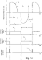
- Figs. 3A and 3B show example waveforms illustrating the operation of the dimmer switch 100
- the dimmer switch 100 comprises a bidirectional semiconductor switch 110 coupled between the hot terminal H and the dimmed hot terminal DH for generating the phase-control voltage V PC (as shown in Figs. 3A and 3B ) and controlling of the amount of power delivered to the LED driver 102.
- the bidirectional semiconductor switch 110 comprises a control input (e.g., a gate), which may receive control signals for rendering the bidirectional semiconductor switch conductive and non-conductive.
- the bidirectional semiconductor switch 110 may comprise a single device, such as a triac, or a combination of devices, such as, two field-effect transistors (FETs) coupled in anti-series connection.
- the phase-control voltage V PC comprises a forward phase-control voltage.
- the phase-control voltage V PC has a magnitude of approximately zero volts at the beginning of each half cycle during a non-conduction time T NC , and has a magnitude equal to approximately the magnitude of the AC line voltage V AC of the AC power source 105 during the rest of the half cycle, i.e., during a conduction time T CON .
- the conduction time T CON may be approximately two milliseconds when the target intensity L TRGT of the LED light source 104 is at the low-end intensity L LE and approximately seven milliseconds when the target intensity L TRGT is at the high-end intensity L HE .
- the dimmer switch 100 comprises a mechanical air-gap switch S112 electrically coupled to the hot terminal H and in series with the bidirectional semiconductor switch 110, such that the LED light source 104 is turned off when the switch is open.
- the air-gap switch S112 is closed, the dimmer switch 100 is operable to control the bidirectional semiconductor switch 110 to control the amount of power delivered to the LED driver 102.
- the air-gap switch S112 is mechanically coupled to the rocker switch 116 of the user interface of the dimmer switch 100, such that the switch may be opened and closed in response to actuations of the rocker switch.
- the dimmer switch 100 further comprises a rectifier circuit 114 coupled across the bidirectional semiconductor switch 110 and operable to generate a rectified voltage V RECT (i.e., a signal representative of the voltage developed across the bidirectional semiconductor switch).
- the dimmer switch 100 comprises an analog control circuit 115 including a power supply 120, a constant-rate one-shot timing circuit 130, and a variable-threshold trigger circuit 140 (i.e., a gate drive circuit).
- the control circuit 115 receives the rectified voltage V RECT from the rectifier circuit 114 and conducts a control current I CNTL through the load (i.e., the LED driver 102) in order to generate a drive voltage V DR (i.e., a drive signal) for controlling the bidirectional semiconductor switch 110 to thus adjust the intensity of the LED light source 104 in response to the intensity adjustment actuator 118.
- the power supply 120 of the control circuit 115 conducts a charging current I CHRG through the LED driver 102 in order to generate a supply voltage V CC (e.g., approximately 11.4 volts).
- V CC e.g., approximately 11.4 volts.
- the charging current I CHRG of the power supply makes up a portion of the control current I CNTL of the control circuit 115.
- the timing circuit 130 receives the supply voltage V CC and generates a timing voltage V TIM (i.e., a timing signal), which comprises a ramp signal having a constant rate of increasing magnitude (i.e., a constant positive slope) as shown in Figs. 3A and 3B .
- V TIM i.e., a timing signal
- the timing circuit 130 also receives the rectified voltage V RECT and is able to derive zero-crossing timing information from the voltage developed across the LED driver 102 (i.e., from the control current I CNTL conducted through the LED driver 102).
- the timing voltage V TIM begins increasing from approximately zero volts shortly after the zero-crossings of the AC line voltage V AC (i.e., shortly after the beginning of each half cycle as shown at times t 1 , t4 in Figs. 3A and 3B ) and continues increasing at the constant rate.
- T TIM time i.e., the timing voltage V TIM started increasing from zero volts during the present half cycle
- the timing voltage V TIM is driven to approximately zero volts near the next zero-crossing (i.e., near the end of the present half cycle as shown at time t 3 in Figs. 3A and 3B ). Since the timing voltage V TIM increases in magnitude at the constant rate for the fixed amount of time T TIM each half cycle, the timing voltage V TIM is essentially identical during each half cycle as shown in Figs. 3A and 3B .
- variable-threshold trigger circuit 140 receives the timing voltage V TIM from the timing circuit 130, and generates a drive voltage V DR (i.e., a gate drive voltage) for controlling the bidirectional semiconductor switch 110 to thus adjust the intensity of the LED light source 104 in response to actuations of the intensity adjustment actuator 118.
- the trigger circuit 140 is characterized by a variable threshold (i.e., a variable threshold voltage V TH shown in Figs. 3A and 3B ) that may be adjusted in response to the intensity adjustment actuator 118 of the user interface of the dimmer switch 100.
- a gate coupling circuit 150 couples the drive voltage V DR to the gate of the bidirectional semiconductor switch 110 for thus rendering the bidirectional semiconductor switch 110 conductive and non-conductive in response to the magnitude of the variable threshold voltage V TH .
- the trigger circuit 140 is operable to drive the drive voltage V DR to a first magnitude (e.g., approximately zero volts as shown in Figs. 3A and 3B ) to thus render the bidirectional semiconductor switch 110 conductive each half cycle (as will be described in greater detail below with reference to Fig. 4 ).
- the drive voltage V DR is then driven to a second magnitude (e.g., approximately the supply voltage V CC as shown in Figs. 3A and 3B ) to render the bidirectional semiconductor switch 110 non-conductive when the timing voltage V TIM is controlled to approximately zero volts shortly before the next zero-crossing.
- the variable threshold voltage V TH is shown at two different magnitudes in Figs. 3A and 3B , which results in the drive voltage V DR being driven low to zero volts (and thus rendering the bidirectional semiconductor switch 110 conductive) for different amounts of time.
- the control circuit 115 of the dimmer switch 100 is operable to provide a constant gate drive to the bidirectional semiconductor switch 110 by maintaining the drive voltage V DR low for the remainder of the half cycle after the bidirectional semiconductor switch 110 is rendered conductive (as shown at firing times t 2 , t 5 ). Accordingly, the bidirectional semiconductor switch 110 will remain conductive independent of the magnitude of the load current I LOAD conducted through the bidirectional semiconductor switch and the LED driver 102. When the bidirectional semiconductor switch 110 is conductive and the magnitude of the phase control voltage V PC is greater than approximately the magnitude of the bus voltage V BUS of the LED driver 102, the LED driver 102 will begin to conduct the load current I LOAD through the bidirectional semiconductor switch.
- the magnitude of the load current I LOAD may quickly peak before subsiding down to a substantially small magnitude (e.g., approximately zero amps).
- the bidirectional semiconductor switch 110 will remain conductive independent of the magnitude of the load current I LOAD because the control circuit 115 is providing constant gate drive to the bidirectional semiconductor switch.
- the load current I LOAD may also change direction after the bidirectional semiconductor switch 110 is rendered conductive.
- the bidirectional semiconductor switch 110 is also operable to conduct current in both directions (i.e., to and from the LED driver 102) after the bidirectional semiconductor switch is rendered conductive during a single half cycle, thereby allowing any capacitors in the filter network 108 of the LED driver 102 to follow the magnitude of the AC line voltage V AC of the AC power source 105.
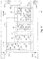
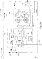
- Fig. 4 is a simplified schematic diagram of the dimmer switch 100.
- the bidirectional semiconductor switch 110 of the dimmer switch 100 of the first example is implemented as a triac 110', but may alternatively be implemented as one or more silicon-controlled rectifiers (SCRs), or any suitable thyristor.
- the triac 110' comprises two main terminals that are coupled in series electrical connection between the hot terminal H and the dimmed hot terminal DH, such that the triac is adapted to be coupled in series electrical connection between the AC power source 105 and the LED driver 102 for conducting the load current I LOAD to the LED driver.
- the triac 110' comprises a gate (i.e., a control input) for rendering the triac conductive each half cycle of the AC power source 105 as will be described in greater detail below. While not shown in Fig. 4 , a choke inductor may be coupled in series with the triac 110', and a filter circuit (such as a filter capacitor) may be coupled between the hot terminal H and the dimmed hot terminal DH (i.e., in parallel with the triac) to prevent noise generated by the switching of the triac from being conducted on the AC mains wiring.
- a gate i.e., a control input
- a choke inductor may be coupled in series with the triac 110'
- a filter circuit such as a filter capacitor
- the rectifier circuit 114 comprises a full-wave rectifier bridge having four diodes D114A, D114B, D114C, D114D.
- the rectifier bridge of the rectifier circuit 114 has AC terminals coupled in series between the hot terminal H and the dimmed hot terminal DH, and DC terminals for providing the rectified voltage V RECT to the timing circuit 130 when the triac 110' is non-conductive and a voltage is developed across the dimmer switch 100.
- the control circuit 115 conducts the control current I CNTL through the rectifier circuit 114 and the LED driver 102.
- the total current conducted through the LED driver 102 each half cycle is the sum of the load current I LOAD conducted through the bidirectional semiconductor switch 110, the control current I CNTL conducted through the control circuit 115 of the dimmer switch 100, and any leakage current conducted through the filter circuit (that may be coupled between the hot terminal H and the dimmed hot terminal DH).
- the power supply 120 comprises, for example, a pass-transistor circuit that generates the supply voltage V CC .
- the pass-transistor circuit comprises an NPN bipolar junction transistor Q122 having a collector coupled to receive the rectifier voltage V RECT through a resistor R124 (e.g., having a resistance of approximately 100 k ⁇ ).
- the base of the transistor Q122 is coupled to the rectifier voltage V RECT through a resistor R125 (e.g., having a resistance of approximately 150 kQ), and to circuit common through a zener diode Z126 (e.g., having a break-over voltage of approximately 12 volts).
- the power supply 120 further comprises a storage capacitor C128, which is able to charge through the transistor Q122 to a voltage equal to approximately the break-over voltage of the zener diode Z126 minus the base-emitter drop of the transistor Q122.
- the storage capacitor C128 has, for example, a capacitance of approximately 10 ⁇ F, and operates to maintain the supply voltage V CC at an appropriate magnitude (i.e., approximately 11.4 volts) to allow the timing circuit 120 to generate the timing voltage V TIM and the gate coupling circuit 150 to continue rendering the triac 110' conductive after the firing times each half cycle.
- the timing circuit 130 comprises a constant ramp circuit 160, a one-shot latch circuit 170, and a reset circuit 180.
- the constant ramp circuit 160 receives the supply voltage V CC and causes the timing voltage V TIM to increase in magnitude at the constant rate.
- the reset circuit 180 receives the rectified voltage V RECT and is coupled to the timing voltage V TIM , such that the reset circuit is operable to start the timing voltage V TIM increasing in magnitude from approximately zero volts shortly after the beginning of each half cycle at a half cycle start time (e.g., times t 1 , t4 in Figs. 3A and 3B ).
- the reset circuit 180 is operable to enable the timing voltage V TIM (i.e., to start the increase of the magnitude of the timing voltage V TIM ) in response to a positive-going transition of the rectified voltage V RECT across a reset threshold V RST that remains above the reset threshold V RST for at least a predetermined amount of time.
- the one-shot latch circuit 170 provides a latch voltage V LATCH to the reset circuit 180 to prevent the reset circuit 180 from resetting the timing voltage V TIM until the end of the half cycle, thus ensuring that the reset circuit only restarts the generation of the timing voltage once each half cycle.
- the one-shot latch circuit 170 stops the generation of the timing voltage V TIM by controlling the magnitude of the timing voltage V TIM to approximately 0.6 volts at the end of the fixed amount of time from when the reset circuit 180 enabled the timing voltage V TIM (e.g., near the end of the half cycle at time t 3 in Figs. 3A and 3B ).
- the reset circuit 180 is once again able to enable the generation of the timing voltage V TIM after the beginning of the next half cycle (i.e., at time t 4 in Figs. 3A and 3B ).
- a dead time T DT exists between the time when the one-shot latch circuit 170 drives the timing voltage V TIM to approximately 0.6 volts and the reset circuit 180 enables the generation of the timing voltage V TIM by controlling the magnitude of the timing voltage V TIM down to approximately zero volts.
- the variable-threshold trigger circuit 140 comprises a comparator U142 having an inverting input that receives the timing voltage V TIM from the timing circuit 130.
- the variable-threshold trigger circuit 140 also comprises a potentiometer R144 that is mechanically coupled to the slider knob of the intensity adjustment actuator 118.
- the potentiometer R144 has a resistive element coupled between the supply voltage V CC and circuit common and a wiper terminal that generates the variable threshold voltage V TH .
- the variable threshold voltage V TH comprises a DC voltage that varies in magnitude in response to the position of the slider knob of the intensity adjustment actuator 118 and is provided to a non-inverting input of the comparator U142.
- the drive voltage V DR is generated at an output of the comparator U142 and is provided to the gate coupling circuit 150 for rendering the triac 110' conductive and non-conductive.
- the gate coupling circuit 150 comprises an opto-coupler U152 having an input photodiode, which is coupled between the supply voltage V CC and the output of the comparator U142 and in series with a resistor R154 (e.g., having a resistance of approximately 82 k ⁇ ).
- the opto-coupler U152 has an output phototriac that is coupled in series with a resistor R156 (e.g., having a resistance of approximately 100 ⁇ ).
- the series combination of the output phototriac of the opto-coupler U152 and the resistor R156 is coupled between the gate and one of the main terminals of the triac 110' (e.g., to the hot terminal H).
- the magnitude of the drive voltage V DR at the output of the comparator U142 of the variable-threshold trigger circuit 140 remains high at approximately the supply voltage V CC , such that the triac 110' remains non-conductive.
- the comparator U142 drives the drive voltage V DR low to approximately circuit common, such that the input photodiode of the opto-coupler U152 conducts a drive current I DR , which may have an rated magnitude I DR-RTD of approximately 2mA.
- the output phototriac of the opto-coupler U152 is rendered conductive and conducts a gate current I G through the gate of the triac 110', thus rendering the triac conductive.
- the drive voltage V DR is driven low to render the triac 110' conductive after a variable amount of time has elapsed since the half cycle start time (i.e., the non-conduction time T NC as shown in Figs. 3A and 3B ), where the variable amount of time is adjusted in response to intensity adjustment actuator 118 and the variable threshold voltage V TH .
- the input photodiode of the opto-coupler U152 continues to conduct the drive current I DR for the remainder of the half cycle.
- the input photodiode of the opto-coupler U152 may conduct an average current from the storage capacitor C128 of the power supply 120 where the average current may range from approximately 0.5 milliamps when the target intensity L TRGT of the LED light source 104 is at the low-end intensity L LE to approximately 1.7 milliamps when the target intensity L TRGT is at the high-end intensity L HE .
- the load current I LOAD may change direction after the triac 110' is rendered conductive (i.e., the magnitude of the load current I LOAD transitions from positive to negative or vice versa).
- the triac commutates off and becomes non-conductive.
- the gate of the triac 110' stops conducting the gate current I G and the output phototriac of the opto-coupler U152 becomes non-conductive.
- the input photodiode of the opto-coupler U152 continues to conduct the drive current I DR (i.e., providing a constant gate drive) even when the triac 110' becomes non-conductive, the output phototriac of the opto-coupler is able to conduct the gate current I G and the triac 110' is able to be rendered conductive and conduct the load current I LOAD in the opposite direction shortly thereafter. Accordingly, the triac 110' is able to conduct the load current I LOAD in both directions in a single half cycle.
- the timing circuit 130 continues to generate the timing voltage V TIM .
- the magnitude of the timing voltage V TIM remains above the variable threshold voltage V TH and the triac 110' remains conductive until approximately the end of the half cycle when the one-shot latch circuit 170 drives the timing voltage to approximately zero volts.
- the input photodiode of the opto-coupler U152 continues to conduct the drive current I DR and the output phototriac continues to conduct the gate current I G to render the triac 110' conductive while the drive voltage V DR is driven low each half cycle (as shown in Figs. 3A and 3B ).
- the latch circuit 170 is operable to control the timing voltage V TIM to approximately zero volts (thus controlling the magnitude of the drive voltage V DR high to approximately the supply voltage V CC ) shortly before the end of the present half cycle (as shown at time t 3 in Figs. 3A and 3B ). Accordingly, the length of the timing voltage V TIM (i.e., the fixed amount of time T TIM ) is slightly smaller than the length T HC of each half cycle.
- the dead time T DT (or "blanking pulse") in the timing voltage V TIM at the end of the half cycle allows the triac 110' to commutate off (i.e., become non-conductive) when the magnitude of the load current I LOAD through the triac reduces to approximately zero amps at the end of the half cycle.
- the reset circuit 180 only starts the timing voltage V TIM after a zero-crossing of the AC mains lines voltage V AC , i.e., in response to the magnitude of the rectified voltage V RECT exceeding the reset threshold V RST when the rectified voltage is increasing in magnitude.
- the reset circuit 180 is prevented from resetting the timing voltage V TIM in response to the magnitude of the rectified voltage V RECT dropping below the reset threshold V RST , which may or may not happen each half cycle due to the capacitive input impedance of the LED driver 102.
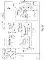
- Fig. 5 is a simplified schematic diagram of the timing circuit 130.
- the constant ramp circuit 160 receives the supply voltage V CC and generates the timing voltage V TIM across a timing capacitor C162 (e.g., having a capacitance of approximately 50 nF).
- the constant ramp circuit 160 comprises a constant current source for conducting a constant timing current I TIM through the timing capacitor C162, such that the timing voltage V TIM has a constant slope.
- the constant current source circuit comprises a PNP bipolar junction transistor Q164 having an emitter coupled to the supply voltage V CC via a resistor R165 (e.g. having a resistance of approximately 10 k ⁇ ).
- Two diodes D166, D168 are coupled in series between the supply voltage V CC and the base useful transistor Q164.
- a resistor R169 is coupled between the base of the transistor Q164 and circuit common and has, for example, a resistance of approximately 51 k ⁇ .
- a voltage having a magnitude of approximately the forward voltage drop of the diode D166 (e.g., approximately 0.6 V) is produced across the resistor R165, such that the resistor conducts the constant timing current I TIM (e.g., approximately 70 ⁇ A) into the capacitor C162.
- the one-shot latch circuit 170 comprises a comparator U172 having an inverting input coupled to the timing voltage V TIM .
- the timing voltage V TIM is further coupled to an output of the comparator U172 via a diode D174.
- the one-shot latch circuit 170 includes a resistive divider, which is coupled in series electrical connection between the supply voltage V CC and circuit common, and comprises two resistors R175, R176 having, for example, resistances of approximately 100 k ⁇ and 1 M ⁇ , respectively.
- the junction of the two resistors R175, R176 produces a latch threshold voltage V TH-L , which is provided to a non-inverting input of the comparator U172.
- the non-inverting input of the comparator U172 is also coupled to the output via a resistor R178 (e.g., having a resistance of approximately 1 k ⁇ ).
- the latch voltage V LATCH is generated at the output of the comparator U172 and is provided to the reset circuit 180 as will be described in greater detail below.
- the reset circuit 180 comprises a first comparator U181 having a non-inverting input that receives the rectified voltage V RECT via the series combination of a zener diode Z182 and a resistor R183 (e.g., having a resistance of approximately 100 k ⁇ ).
- the parallel combination of a capacitor C184 (e.g., having a capacitance of approximately 1000 pF) and a resistor R185 (e.g., having a resistance of approximately 20 k ⁇ ) is coupled between the non-inverting input of the comparator U181 and circuit common.
- a zener diode Z186 (e.g., having a break-over voltage of approximately 12 volts) clamps the magnitude of the voltage produced between the non-inverting input of the comparator U181 and circuit common.
- the reset circuit 180 further comprises a resistive divider that has two resistors R187, R188 (e.g., having resistances of approximately 150 k ⁇ and 100 k ⁇ , respectively), and is coupled in series electrical connection between the supply voltage V CC and circuit common.
- the junction of the two resistors R187, R188 produces a reset threshold voltage V RST (e.g., approximately 4.8 V), which is provided to an inverting input of the comparator U181.
- An output of the comparator U181 is coupled to the supply voltage V CC via a resistor R189 (e.g., having a resistance of approximately 10 k ⁇ ).
- the reset circuit 180 also comprises a second comparator U191 having a non-inverting input coupled to the threshold voltage V RST and an output coupled to the timing voltage V TIM .
- the output of the comparator U181 is coupled to an inverting input of the second comparator U191 via a capacitor C190 (e.g., having a capacitance of approximately 1000 pF).
- a resistor R192 e.g., having a resistance of approximately 68 k ⁇
- a diode D193 are coupled between the inverting input of the comparator U191 and circuit common.
- a FET Q194 is also coupled between the inverting input and circuit common.
- the gate of the FET Q194 is pulled up towards the supply voltage V CC through a resistor R195 (e.g., having a resistance of approximately 100 k ⁇ ), and is coupled to the latch voltage V LATCH , such that the FET may be rendered conductive and non-conductive in response to the one-shot latch circuit 170.
- a resistor R195 e.g., having a resistance of approximately 100 k ⁇
- the inverting input of the comparator U172 of the latch circuit 170 is less than the latch threshold voltage V TH-L (e.g., approximately 10.5 V) at the non-inverting input and the output is pulled up towards the supply voltage V CC via the resistor R195 and the diode D196 of the reset circuit 180.
- the magnitude of the timing voltage V TIM continues to increase at the constant rate until the magnitude of timing voltage exceeds the latch threshold voltage V TH-L , at which time, the comparator U172 of the latch circuit 170 drives the output low to approximately zero volts.
- the magnitude of the timing voltage V TIM is reduced to approximately the forward voltage drop of the diode D174 (e.g., approximately 0.6 V). Accordingly, the fixed amount of time T TIM that the timing voltage V TIM is generated each half cycle is a function of the constant rate at which the magnitude of the timing voltage V TIM increases with respect to time dV TIM /dt (i.e., approximately 1.4 V/msec) and the magnitude of the latch threshold voltage V TH-L (i.e., approximately 10.5 V), such that the fixed amount of time T TIM is approximately 7.5 msec each half cycle.
- the latch threshold voltage V TH-L is reduced to approximately 0.1 V, such that the comparator U172 continues to drive the output low and the magnitude of the timing voltage V TIM is maintained at approximately 0.6 V.
- the magnitude of the rectified voltage V RECT is below a break-over voltage of the zener diode Z182 of the reset circuit 180 (e.g., approximately 30 V) and the voltage at the non-inverting input of the first comparator U181 is approximately zero volts, such that the output of the first comparator is driven low towards circuit common.
- the capacitor C184 begins to charge until the magnitude of the voltage at the non-inverting input of the first comparator U181 exceeds the reset threshold voltage V RST .
- the output of the first comparator U181 is then driven high towards the supply voltage V CC and the capacitor C190 conducts a pulse of current into the resistor R192, such that the magnitude of the voltage at the inverting input of the second comparator U191 exceeds the reset threshold voltage V RST , and the second comparator pulls the timing voltage V TIM down towards circuit common (i.e., the magnitude of the timing voltage is controlled from approximately 0.6 volts to zero volts).
- the magnitude of the voltage at the inverting input of the comparator U 172 of the latch circuit 170 is now less than the latch threshold voltage V TH-L (i.e., approximately 0.1 V), and the comparator stops pulling the timing voltage V TIM down towards circuit common.
- the reset circuit 180 only drives the timing voltage V TIM low for a brief period of time (e.g., approximately 68 ⁇ sec) before the capacitor C190 fully charges and then stops conducting the pulse of current into the resistor R192. Accordingly, the second comparator U191 then stops pulling the timing voltage V TIM down towards circuit common, thus allowing the timing voltage to once again begin increasing in magnitude with respect to time at the constant rate.
- a brief period of time e.g., approximately 68 ⁇ sec
- the comparator U172 of the latch circuit 170 stops pulling the timing voltage V TIM down towards circuit common and the magnitude of the latch voltage V LATCH is pulled high towards the supply voltage V CC via the resistor R195 and the diode D196.
- the FET Q194 is rendered conductive, thus maintaining the inverting input of the second comparator U191 less than the reset threshold voltage V RST .
- the FET Q194 is rendered non-conductive when the comparator U172 of the one-shot latch circuit 170 pulls the timing voltage V TIM low near the end of the half cycle.
- the FET Q194 is rendered conductive for most of each half cycle and prevents the reset circuit 180 from resetting the generation of the timing voltage V TIM until after the latch circuit 170 ceases the generation of the timing voltage, thereby greatly improving the noise immunity of the dimmer switch 100 with respect to impulse noise on the AC line voltage V AC .
- the reset circuit 180 does not reset the generation of the timing voltage V TIM until the magnitude of the voltage at the non-inverting input of the first comparator U181 of the reset circuit 170 rises above the reset threshold voltage V RST at the beginning of the next half cycle.
- control circuit 115 of the dimmer switch 100 of the first example useful for understanding the invention conducts a control current through the LED driver 102 and provides constant gate drive to the bidirectional semiconductor switch 110 after the bidirectional semiconductor switch is rendered conductive.
- the control circuit 115 is operable to derive zero-crossing timing information from the voltage developed across the LED driver 102, and thus from the control current I CNTL conducted through the LED driver 102.
- the average magnitude of the control current I CNTL conducted through the LED driver 102 is approximately equal to the sum of the average magnitude of the timing current I TIM and the drive current I DR , as well as the other currents drawn by the timing circuit 130 and the trigger circuit 140.
- the control circuit 115 is operable to render the bidirectional semiconductor switch 110 conductive each half cycle in response to the variable threshold that is representative of the desired intensity of the LED light source 104 and to maintain the bidirectional semiconductor switch conductive until approximately the end of the present half cycle.
- the conduction time T CON of the drive voltage V DR generated by the trigger circuit 140 has a length that is not dependent upon the length of the fixed amount of time T TIM that the timing circuit 130 generates the timing signal V TIM .
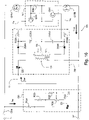
- Fig. 6 is a simplified schematic diagram of a dimmer switch 200 according to a second example useful for understanding the invention.
- Fig. 7 shows example waveforms illustrating the operation of the dimmer switch 200.
- the bidirectional semiconductor switch of the dimmer switch 200 of the second example is implemented as two individual MOS-gated transistors, e.g., FETs Q210A, Q210B, coupled in anti-series connection between the hot terminal H and the dimmed hot terminal DH for control of the amount of power delivered to the LED driver 102.
- the sources of the FETs Q210A, Q210B are coupled together at circuit common.
- the FETs Q210A, Q210B may comprise metal-oxide semiconductor FETs (MOSFETs) or may alternatively be replaced by any suitable voltage-controlled semiconductor switches, such as, for example, insulated gate bipolar junction transistors (IGBTs).
- the FETs Q210A, Q210B have control inputs (i.e., gates) that are coupled to a gate coupling circuit 250, which comprises respective gate resistors R252, R254 (e.g., each having a resistance of approximately 47 ⁇ ) for coupling to the gates of the FETs a drive voltage V DR-INV .
- the drive voltage V DR-INV as shown in Fig.
- Each FET Q210A, Q210B is rendered conductive when the voltage at the gates of the FET is driven to a rated gate threshold voltage (e.g., approximately 10 volts).
- the FETs Q210A, Q210B are simultaneously controlled to be conductive and non-conductive using the forward phase-control technique, and are operable to be rendered conductive and to remain conductive independent of the magnitude of the load current I LOAD conducted through the FETs.
- the dimmer switch 200 comprises a full-wave rectifier bridge that includes the body diodes of the two FETs Q210A, Q210B in addition to two diodes D214A, D214B.
- the timing circuit 130 of the dimmer switch 200 of the second embodiment operates in the same manner as in the first example
- the dimmer switch 200 comprises an analog control circuit 215 having a variable-threshold trigger circuit 240 that is similar to the variable-threshold trigger circuit 140 of the first example
- the trigger circuit 240 of the second example comprises a comparator U242 having a non-inverting input that receives the timing voltage V TIM and an inverting input that receives a variable threshold voltage V TH from a potentiometer R244.
- the trigger circuit 240 operates to drive the drive voltage V DR-INV high towards the supply voltage V CC to render the FETs Q210A, Q210B conductive, and low towards circuit common to render the FETs non-conductive (as shown in Fig. 7 ).
- the gates of the FETs Q210A, Q210B only conduct a small pulse of drive current I DR-INV from the power supply 120 when the FETs Q210A, Q210B are rendered conductive, i.e., due to the charging of the input capacitances of the gates of the FETs (which each may have, for example, an input capacitance of approximately 100 pF).
- the average magnitude of the control current I CNTL conducted through the LED driver 102 by the analog control circuit 215 of the dimmer switch 200 of the second example is less than the average magnitude of the control current I CNTL conducted by the analog control circuit 115 of the dimmer switch 100 of the first example (which conducts the drive current I DR through the input photodiode of the opto-coupler U152 for the entire time that the triac 110' is rendered conductive).
- the dimmer switch 200 of the second example does not require the opto-coupler U152 of the first example, which is typically expensive and is also characterized by a rated turn-on time (e.g., approximately 35 microseconds).
- the rated turn-on time of the opto-coupler U152 limits how quickly the triac 110' can be rendered conductive after becoming non-conductive. Specifically, during the time from when the triac 110' becomes momentarily non-conductive and is once again rendered conductive, the magnitude of the phase-control voltage V PC across the LED driver 102 decreases while the magnitude of the voltage across the dimmer switch 100 increases.
- This change in the voltage across the input of the LED driver 102 may result in fluctuations in the intensity of the LED light source 104 (or fluorescent lamp) for some high-efficiency lighting loads.
- the bidirectional semiconductor switch of the dimmer switch 200 is implemented as FETs Q210A, Q210B and because the FETs Q210A, Q210B are operable to remain conductive independent of the magnitude of the load current, potential fluctuations in the intensity of some high-efficiency lighting loads are avoided.
- Fig. 8 is a simplified schematic diagram of a dimmer switch 300 according to a third example useful for understanding the invention.
- the dimmer switch 300 of the third example comprises the triac 110' (as in the first example).
- the dimmer switch 300 includes a gate coupling circuit 350 that comprises a voltage-controlled controllably conductive device, such as two MOS-gated transistors (e.g., FETs Q352A, Q352B) coupled in anti-series connection between the gate and a first one of the main load terminals of the triac 110' (e.g., the hot terminal H of the dimmer switch).
- a voltage-controlled controllably conductive device such as two MOS-gated transistors (e.g., FETs Q352A, Q352B) coupled in anti-series connection between the gate and a first one of the main load terminals of the triac 110' (e.g., the hot terminal H of the dimmer switch).
- the FETs Q352A, Q352B may comprise MOSFETs or may alternatively be replaced by any suitable voltage-controlled semiconductor switches, such as, for example, IGBTs.
- the sources of the FETs Q352A, Q352B are coupled together through two source resistors R353, R354 (e.g., each having a resistance of approximately 10 ⁇ ), where the junction of the two resistors R353, R354 is coupled to circuit common.
- the source resistors R353, R354 operate to limit the magnitude of the gate current I G conducted through the gate of the triac 110'to a maximum gate current (e.g., approximately 0.6 amp).
- the gates of the FETs Q352A, Q352B are coupled to respective gate resistors R355, R356 (e.g., each having a resistance of approximately 47 ⁇ ).
- the drive voltage V DR-INV generated by the analog control circuit 215 is received at a control input of the gate coupling circuit 350 (i.e., the junction of the gate resistors R355, R356).
- the dimmer switch 300 comprises a resistor R358, which has a resistance of, for example, approximately 30.9 ⁇ and is coupled between the gate and a second one of the main load terminals of the triac 110' (e.g., to the dimmed hot terminal DH of the dimmer switch).
- the dimmer switch 300 further comprises a full-wave rectifier bridge that includes the body diodes of the FETs Q352A, Q352B and the diodes D214A, D214B, and generates the rectified voltage V RECT that is received by the power supply 120 and the timing circuit 130 of the control circuit 215.
- control circuit 215 is coupled to the first main load terminal of the triac 110' through the body diode of the FET Q352A and the diode D214A, and to the second main load terminal of the triac through the body diode of the FET Q352B, the diode D214B, and the resistor R358.
- control circuit 215 could be directly coupled to at least one of the main load terminals of the triac 110', or electrically coupled to at least one of the main load terminals of the triac through one or more resistors.
- the timing circuit 130 of the control circuit 215 generates the timing voltage V TIM and the variable-threshold trigger circuit 240 generates the drive voltage V DR-INV as in the second example (as shown in Fig. 7 ).
- the FETs Q352A, Q352B are non-conductive, such that the triac 110' is also non-conductive.
- the trigger circuit 240 drives the drive voltage V DR-INV high towards the supply voltage V CC at the firing time each half cycle, the FETs Q352A, Q352B are able to conduct the gate current I G through the gate of the triac 110' to render the triac conductive.
- the drive voltage V DR-INV is driven low slightly before the end of the half cycle, such that the blanking pulse exists at the end of the half cycle to allow the triac 110' to commutate off. Since the drive voltage V DR-INV remains high until approximately the end of the half-cycle, the FETs Q352A, Q352B remain conductive such that the FETs Q352A, Q352B are able to conduct the gate current I G at any time from the firing time through approximately the remainder of the half cycle.
- the triac 110' is rendered conductive from the firing time to approximately the end of the half cycle, thereby allowing the load current I LOAD to be either polarity (i.e., positive or negative) in any given half cycle, which is particularly important when the LED driver 102 has a capacitive impedance and causes the load current to change polarity before one of the zero-crossings.
- the control input of the gate coupling circuit 350 only conducts the small pulses of drive current I DR-INV from the power supply 120 when the FETs Q352A, Q352B are rendered conductive due to the charging of the input capacitances of the gates of the FETs (i.e., as shown in Fig. 7 ).
- the gate coupling circuit 350 allows the analog control circuit 215 to render the triac 110' conductive and maintain the triac conductive without the need to conduct the drive current I DR-INV through the control input of the gate coupling circuit during approximately the remainder of the half cycle (e.g., in contrast to the input photodiode of the optocoupler U152 of the first embodiment conducting the drive current I DR as shown in Figs.
- the average magnitude of the control current I CNTL conducted by the analog control circuit 215 of the dimmer switch 300 of the third embodiment to render the triac 110' conductive is less than the average magnitude of the control current I CNTL conducted by the analog control circuit 115 of the dimmer switch 100 of the first embodiment to render the triac 110' conductive.
- the gate coupling circuit 350 may conduct an average current of approximately 240 nanoamps from the storage capacitor C128 of the power supply 120 (independent of the target intensity L TRGT of the LED light source 104).
- the dimmer switch 300 of the third example does not require the opto-coupler U152 to render the triac 110' conductive.
- the opto-coupler U152 is typically expensive and is characterized by the rated turn-on time, which limits how quickly the triac 110' can be rendered conductive after becoming non-conductive in response to the load current I LOAD changing directions.
- the FETs Q352A, Q352B of the third example may be sized smaller in power rating (and accordingly, in physical size) than the FETs Q210A, Q210B of the dimmer switch 200 of the second example (which conduct the load current I LOAD ).
- the FETs Q352A, Q352B of the third example do not conduct the load current I LOAD , the FETs need not be power devices, but can rather be signal-level devices.
- the dimmer switch 300 of the third example only requires one power device (i.e., the triac 110') rather than two power devices (i.e., the FETs Q210A, Q210B), which leads to lower total cost of the dimmer switch 300, as well as fewer constraints to physically fit and heat sink two power devices in a single wall-mounted load control device.
- the triac 110' typically has better peak current capabilities in a single package as compared to the two FETs Q210A, Q210B having similar sized packages.
- the triac 110' and the gate coupling circuit 350 of the dimmer switch 300 of the third example provide a thyristor-based load control circuit that requires substantially no net average current to be conducted through the control input after the triac is rendered conductive through the remainder of the half-cycle using a constant gate drive signal.
- substantially no net average current is defined as an amount of current appropriate to charge the input capacitances of the gates of the FETs Q352A, Q352B (or other suitable switching devices) of the gate coupling circuit 350, for example, less than approximately one microamp.
- Fig. 9 is a simplified block diagram of a reverse-phase control dimmer switch 400 according to a fourth example useful for understanding the invention of the present invention.
- the bidirectional semiconductor switch 110 is implemented as two FETs Q210A, Q210B coupled in anti-series connection (as in the second example).
- the dimmer switch 100 comprises an analog control circuit including a voltage reference circuit 420, a timing circuit 430, and a gate drive circuit 440.
- the voltage reference circuit 420 includes a pass-transistor circuit 460 and a snap-on circuit 470, and operates to generate a reference voltage V REF (e.g., approximately 14.4 volts) from the rectified voltage V RECT .
- V REF reference voltage
- the timing circuit 430 receives the reference voltage V REF and generates a timing voltage V TIM , which is representative of the target intensity L TRGT of the LED light source 104.
- the gate drive circuit 440 generates a gate voltage V G , which is coupled to the gates of the FETs Q210A, Q210B via the gate coupling circuit 250 for simultaneously rendering the FETs conductive and non-conductive.
- the phase-control voltage V PC generated by the dimmer switch 400 comprises a reverse phase-control voltage. Accordingly, the gate drive circuit 440 operates to render the FETs Q210A, Q210B conductive at the beginning of each half cycle, and non-conductive at some time during each half cycle in response to the timing voltage V TIM .
- Fig. 10 is a simplified timing diagram showing examples of the phase-control voltage V PC generated by the dimmer switch 400, the timing voltage V TIM , and the gate voltage V G for driving the FETs Q210A, Q210B according to the fourth example useful for understanding the invention.
- the phase-control voltage V PC has a magnitude equal to approximately the magnitude of the AC line voltage V AC of the AC power source 105 at the beginning of each half cycle during a conduction time T CON , and has a magnitude of approximately zero volts during the rest of the half cycle, i.e., during a non-conduction time T NC .
- the gate drive circuit 440 drives the gate voltage V G high towards the reference voltage V REF at the beginning of each half cycle, such that the FETs Q210A, Q210B are rendered conductive (as shown at time t 1 in Fig. 10 ).
- the timing circuit 430 begins generating the timing voltage V TIM , which comprises a ramp voltage that increases in magnitude with respect to time at a rate representative of the target intensity L TRGT of the LED light source 104 (i.e., in response to the intensity adjustment actuator 118).
- the gate drive circuit 440 When the magnitude of the timing voltage V TIM reaches a maximum timing voltage threshold V T-MAX (e.g., approximately 7.5 volts), the gate drive circuit 440 renders the FETs Q210A, Q210B non-conductive (as shown at time t 2 in Fig. 10 ).
- the rate of the timing voltage V TIM is inversely proportional to the target intensity L TRGT , i.e., the rate of the timing voltage V TIM increases as the target intensity L TRGT decreases, and decreases as the target intensity L TRGT increases.
- the gate drive circuit 440 After the FETs Q210A, Q210B are rendered non-conductive, the gate drive circuit 440 will render the FETs conductive once again at the beginning of the next half cycle (as shown at time t 3 in Fig. 10 ).
- Fig. 11 is a simplified schematic diagram of the dimmer switch 400 according to the fourth example.
- the pass-transistor circuit 460 comprises an NPN bipolar junction transistor Q462 having a collector coupled to receive the rectifier voltage V RECT through a resistor R464 (e.g., having a resistance of approximately 180 ⁇ ).
- the base of the transistor Q462 is coupled to the rectifier voltage V RECT through a resistor R465 (e.g., having a resistance of approximately 470 k ⁇ ), and to circuit common through a zener diode Z466 (e.g., having a break-over voltage of approximately 15 volts).
- the pass-transistor circuit 460 further comprises a storage capacitor C468, which is able to charge through the transistor Q462 and a diode D469 to a voltage equal to approximately the break-over voltage of the zener diode Z466 minus the base-emitter drop of the transistor Q462 and the forward drop of the diode D469.
- the storage capacitor C468 has, for example, a capacitance of approximately 22 ⁇ F, and operates to maintain the reference voltage V REF at an appropriate magnitude (e.g., at least approximately 12 volts) to control the FETs Q210A, Q210B to be conductive (i.e., when there is approximately zero volts generated across the dimmer switch 100) as will be described in greater detail below.
- the snap-on circuit 470 is coupled to the storage capacitor Q468 and comprises a PNP bipolar junction transistor Q472.
- the base of the transistor Q472 is coupled to circuit common through the series combination of a resistor R474 (e.g., having a resistance of approximately 22 k ⁇ ) and a zener diode Z476 (e.g., having a break-over voltage of approximately 12 volts).
- the reference voltage V REF is generated across a capacitor C478, which is coupled between the collector of the transistor Q472 and circuit common and has, for example, a capacitance of approximately 0.1 ⁇ F.
- the snap-on circuit 470 operates such that the reference voltage V REF is only provided across the capacitor C478 when the magnitude of the voltage across the storage capacitor C468 of the pass-transistor circuit 460 exceeds the break-over voltage of the zener diode Z476 plus the emitter-base drop useful transistor Q472.
- the timing circuit 430 receives the reference voltage V REF and generates the timing voltage V TIM across a timing capacitor C432 (e.g., having a capacitance of approximately 10 nF).
- the timing circuit 430 includes a constant current source circuit for charging the capacitor C432 at a constant rate to generate the timing voltage V TIM .
- the constant current source circuit comprises a PNP bipolar junction transistor Q434 having an emitter coupled to the reference voltage V REF via a resistor R435 (e.g. having a resistance of approximately 180 k ⁇ ).
- a voltage divider circuit comprising a potentiometer R436 and two resistors R438, R439 is coupled between the reference voltage V REF and circuit common.
- the potentiometer R436 may have a resistance ranging from approximately 0 to 500 k ⁇ , while the resistors R438, R439 may have resistances of approximately 100 k ⁇ and 82 k ⁇ , respectively.
- the junction of the potentiometer R436 and the resistor R438 is coupled to the base of the transistor Q434.
- the resistance of the potentiometer R436 varies in response to the intensity adjustment actuator 118 of the dimmer switch 100, such that the magnitude of the voltage at the base of the transistor Q434 is representative of the target intensity L TRGT .
- the potentiometer R436 When the potentiometer R436 is not presently being adjusted (i.e., is in a steady state condition), a constant voltage is generated across the resistor R435 and the emitter-base junction of the transistor Q434, such that the transistor Q434 conducts a constant current (having a magnitude dependent upon the magnitude of the voltage at the base of the transistor Q434). Accordingly, the capacitor C432 charges at a rate dependent upon the target intensity L TRGT thus generating the timing voltage V TIM (as shown in Fig. 10 ).
- the gate drive circuit 440 renders the FETs Q210A, Q210B conductive at the beginning of each half cycle, and non-conductive at some time during each half cycle in response to the timing voltage V TIM from the timing circuit 430.
- the gate drive circuit 440 comprises an NPN bipolar junction transistor Q441 and a resistor R442, which is coupled between the collector and base of the transistor Q441 and has a resistance of, for example, approximately 270 k ⁇ .
- a diode D443 is coupled between the emitter and the base of the transistor Q441. At the beginning of each half cycle, the resistor R442 conducts current into the base of the transistor Q441.
- the transistor Q441 is thus rendered conductive and the reference voltage V REF is coupled to the gates of the FETs Q210A, Q210B via the respective gate resistors R252, R254 to thus render the FETs conductive.
- the storage capacitor C468 of the voltage reference circuit 420 maintains the reference voltage V REF at an appropriate magnitude (i.e., at least approximately 14.4 volts) to maintain the FETs Q210A, Q210B conductive and the voltage developed across the dimmer switch 400 is approximately zero volts.
- the timing voltage V TIM is coupled to the base of an NPN bipolar junction transistor Q444 through a zener diode Z445 (e.g., having a break-over voltage of approximately 6.8 volts).
- a zener diode Z445 e.g., having a break-over voltage of approximately 6.8 volts.
- the transistor Q444 is rendered conductive. Accordingly, the gate voltage V G is pulled down towards circuit common through the diode D443 thus rendering the FETs Q210A, Q210B non-conductive.
- the gate drive circuit 440 also comprises an NPN bipolar junction transistor Q446 coupled across the zener diode Z445.
- the base of the transistor Q446 is coupled to the junction of two series-connected resistors R447, R448 (e.g., having resistances of approximately 200 k ⁇ and 10 k ⁇ respectively).
- the resistors R447, R448 form a voltage divider coupled between the rectified voltage V RECT and circuit common.
- the base of the transistor Q446 is also coupled to circuit common via a capacitor C449 (e.g., having a capacitance of approximately 10 nF).
- the FETs Q210A, Q210B are rendered non-conductive (in response to the timing voltage V TIM exceeding the maximum timing voltage threshold V T-MAX )
- the voltage developed across the dimmer switch 400 increases to approximately the magnitude of the AC line voltage V AC of the AC power source 105.
- the voltage at the base of the transistor Q446 increases such that the transistor is rendered conductive.
- the magnitude of the timing voltage V TIM is controlled to approximately zero volts and the transistor Q444 is maintained conductive (thus keeping the FETs Q210A, Q210B non-conductive) until the end of the present half cycle.
- the magnitude of the AC line voltage V AC of the AC power source 105 as well as the magnitude of voltage at the base of the transistor Q446 decrease such that the transistor Q446 is rendered non-conductive. Accordingly, the transistor Q444 is rendered non-conductive and the reference voltage V REF is coupled to the gates of the FETs Q210A, Q210B through the transistor Q441 and the respective gate resistors R252, R254, thus rendering the FETs conductive.
- the timing voltage V TIM of the timing circuit 430 may once again begin increasing in magnitude with respect to time at the rate dependent upon the target intensity L TRGT (as shown in Fig. 10 ).
- Fig. 12 is a simplified schematic diagram of a dimmer switch 480 according to an alternate example useful for understanding the invention.
- the dimmer switch 480 of Fig. 12 is very similar to the dimmer switch 400 of the fourth example.
- the dimmer switch 480 of Fig. 12 comprises a voltage compensation circuit 490, which receives the rectified voltage V RECT and adjusts the timing voltage V TIM to account for changes and fluctuations in the AC line voltage V AC of the AC power source 105 to avoid flickering of the intensity of the LED light source 104.
- the voltage compensation circuit 490 comprises two resistors R492, R494, which are coupled in series between the rectified voltage V RECT and circuit common, and have, for example, resistances of approximately 1 M ⁇ and 98 k ⁇ , respectively.
- a capacitor C496 is coupled between the junction of the resistors R492, R494 and circuit common, and has, for example, a capacitance of approximately 0.22 ⁇ F.
- the capacitor C496 is coupled to the timing voltage V TIM through a resistor R498 (e.g., having a resistance of approximately 560 k ⁇ ).
- the voltage produced across the capacitor C496 is proportional to the magnitude of the AC line voltage V AC of the AC power source 105 when the FETs Q210A, Q210B are non-conductive and the timing voltage V TIM is increasing in magnitude with respect to time.
- the capacitor C496 charges to a steady-state voltage.
- the magnitude of the AC line voltage V AC changes while the FETs Q210A,Q210B are non-conductive during a half cycle (e.g., between times t 2 and t 3 in Fig.
- the magnitude of the voltage across the capacitor C496 will also change, thus resulting in a change in the timing voltage V TIM when the FETs are conductive during the next half cycle (e.g., between times t 3 and t 4 ).
- the magnitude of the AC line voltage V AC increases while the FETs Q210A,Q210B are non-conductive during a half cycle
- the magnitude of the timing voltage V TIM will be greater while the FETs are conductive during the next half cycle, thus causing the FETs to be rendered non-conductive earlier in the next half cycle.
- Fig. 13 is a simplified schematic diagram of a dimmer switch 500 according to a fifth example useful for understanding the invention.
- the dimmer switch 500 comprises a mechanical air-gap switch S514 and two FETs Q510A, Q510B coupled in anti-series connection between the hot terminal H and the dimmed hot terminal DH for generating the phase-control voltage V PC .
- the dimmer switch 500 comprises an analog control circuit (e.g., a timing circuit 520) for generating a timing voltage V TIM representative of the target intensity L TRGT of the LED light source 104, and a gate drive circuit 530 for rendering the FETs Q510A, Q510B conductive and non-conductive in response to the timing voltage V TIM to thus generate the phase-control voltage V PC .
- an analog control circuit e.g., a timing circuit 520
- V TIM representative of the target intensity L TRGT of the LED light source 104
- a gate drive circuit 530 for rendering the FETs Q510A, Q510
- the gate drive circuit 530 is operable to generate two gate voltages V G1 , V G2 for independently controlling the respective FETs Q510A, Q510B on a complementary basis.
- the FETs Q510A, Q510B are rendered conductive when the magnitudes of the respective gate voltages V G1 , V G2 are controlled to a nominal gate voltage V N (e.g., approximately 9 V) and are rendered non-conductive when the magnitudes of the respective gate voltages V G1 , V G2 are controlled to approximately zero volts.
- the dimmer switch 500 further comprises an overcurrent protection circuit 540 for rendering the FETs Q510A, Q510B non-conductive in the event of an overcurrent condition in the FETs.
- Fig. 14 is a simplified timing diagram showing examples of the phase-control voltage V PC generated by the dimmer switch 500 and the gate voltages V G1 , V G2 for driving the FETs Q510A, Q510B, respectively.
- the phase-control voltage V PC comprises a forward phase-control voltage.
- the first FET Q510A is rendered conductive and the second FET Q510B is rendered non-conductive when the first gate voltage V G1 increases from approximately zero volts to the nominal gate voltage V N (as shown at time ti), and the second gate voltage V G2 decreases from the nominal gate voltage V N to approximately zero volts.
- the dimmer switch 500 conducts the load current I LOAD to the LED driver 102 through the first FET Q510A and the body diode of the second FET Q510B.
- the first FET Q510 remains conductive.
- the second FET Q510B is non-conductive and the body diode of the second FET Q510B is reversed-biased, the dimmer switch 500 does not conduct the load current I LOAD at this time.
- the first FET Q510A is rendered non-conductive and the second FET Q510B is rendered conductive when the first gate voltage V G1 decreases from the nominal gate voltage V N to approximately zero volts and the second gate voltage V G2 increases from approximately zero volts to the nominal gate voltage V N (as shown at time t 2 ).
- the dimmer switch 500 conducts the load current I LOAD to the LED driver 102 through the second FET Q510B and the body diode of the first FET Q510A.
- the second FET Q510B remains conductive, the first FET Q510A remains non-conductive, and the body diode of the first FET Q510A is reversed-biased at this time, such that the dimmer switch 500 does not conduct the load current I LOAD until the first FET Q510A is rendered conductive.
- the timing circuit 520 is coupled in series between the hot terminal H and the dimmed hot terminal DH and conducts a timing current I TIM (i.e., a control current) through the LED driver 102 in order to generate the timing voltage V TIM across a capacitor C522 (e.g., having a capacitance of approximately 0.1 ⁇ F).
- the capacitor C522 is operable to charge from the AC power source 105 through resistors R524, R525 (e.g., having resistances of approximately 27 k ⁇ and 10 k ⁇ , respectively) and a potentiometer R526.
- the resistance of the potentiometer R526 may range from, for example, approximately 0 k ⁇ to 300 k ⁇ , and may be controlled by a user of the dimmer switch 500 (e.g., by actuating the slider control) to adjust the target intensity L TRGT of the LED light source 104.
- a calibration resistor R527 is coupled to potentiometer R526 for calibrating the range of the potentiometer, and has a resistance of, for example, approximately 300 k ⁇ . Since the capacitor C522 charges through the potentiometer R526, the rate at which the capacitor C522 charges and thus the magnitude of the timing voltage V TIM are representative of the target intensity L TRGT of the LED light source 104.
- the drive circuit 530 comprises a diac 532 (e.g., having a break-over voltage V BR of approximately 32 volts) and two pulse transformers 534A, 534B.
- the diac 532 is coupled in series with the primary windings of the two pulse transformers 534A, 534B.
- the secondary windings of the pulse transformers 534A, 534B are coupled to respective capacitors C535A, C535B via respective zener diodes Z536A, Z536B (which each have a break-over voltage approximately equal to the nominal gate voltage V N , i.e., approximately 9 V).
- the capacitors C535A, C535B are coupled to the gates of the FETs Q510A, Q510B via gate resistors R538A, R538B, respectively (e.g., having resistances of approximately 47 k ⁇ ).
- the gate resistors R538A, R538B may alternatively have different resistances in order to change the duration of the switching times of the FETs Q510A, Q510B as is well known in the art.
- the diac When the magnitude of the timing voltage V TIM exceeds approximately the break-over voltage V BR of the diac 532, the diac conducts a pulse of current (i.e., a firing current I FIRE as shown in Fig. 13 ) through the primary windings of the pulse transformers 534A, 534B causing secondary voltages V SEC (e.g., approximately 9V) to be generated across the secondary windings of the pulse transformers.
- V SEC secondary voltages
- the capacitor C535A charges from the secondary winding of the first pulse transformer 534A through the zener diode Z536A to approximately the nominal gate voltage V N (i.e., approximately 9 volts).
- the first gate voltage V G1 is driven high from approximately zero volts to the nominal gate voltage V N rendering the first FET Q510A conductive (as shown at time t 1 in Fig. 14 ).
- the first FET Q510A is conductive, while the second FET Q510B is non-conductive. Since the body diode of the second FET Q510B is reversed biased at this time, the dimmer switch 500 does not conduct the load current I LOAD .
- the firing current I FIRE has a negative magnitude, thus causing the secondary voltages V SEC across the secondary windings of the pulse transformers 534A, 534B to also have negative magnitudes.
- the zener diode Z536A is reverse-biased during the negative half cycles, causing the capacitor C535A to discharge through the zener diode Z536A, such that the voltage across the capacitor C535A is driven to approximately zero volts.
- the first gate voltage V G1 is driven low from the nominal gate voltage V N to approximately zero volts rendering the first FET Q510A non-conductive (as shown at time t 2 in Fig. 14 ).
- the zener diode Z536B coupled to the secondary winding of the second pulse transformer 534B is forward-biased in the negative half cycles, such that the capacitor C535B charges to approximately the nominal gate voltage V N and the second FET Q510B is rendered conductive during the negative half cycles (as shown at time t 2 in Fig. 14 ).
- the FETs Q510A, Q510B are driven in a complementary manner, such that -- at all times -- at least one FET is conductive, while the other FET is non-conductive.
- the FETs Q510A, Q510B are driven to be conductive for approximately the period T HC of a half cycle and non-conductive for the period T HC of a half cycle.
- the timing circuit 520 also comprises a diac 528 (e.g., having a break-over voltage of approximately 64V) coupled to the potentiometer R526.
- the diac 528 provides voltage compensation by adjusting the voltage provided to the potentiometer R526 to compensate for variations in the AC line voltage V AC provided by the AC power source 105.
- the diac 528 has a negative impedance transfer function, such that the voltage across the diac increases as the current through the diac decreases.
- the current through the resistor R524 and the diac 528 decreases.
- the drive circuit 530 is characterized as having inherent shorted-FET protection. In the event that one of the FETs Q510A, Q510B fails shorted, the drive circuit 530 is operable to drive the other, non-shorted FET into full conduction, such that the load current I LOAD is not asymmetric. Asymmetric current can cause some types of lighting loads to overheat. For example, if the second FET Q510B fails shorted, the full AC waveform will be provided to the LED driver 102 during the negative half cycles.
- the capacitor C522 of the timing circuit 520 will not charge, the diac 532 of the drive circuit 330 will not conduct the pulse of the firing current I FIRE , and the voltage across the capacitor C535A will not be driven to zero volts to render the first FET Q510A non-conductive during the negative half cycles. Accordingly, the first FET Q510A will remain conductive during both half cycles and the load current I LOAD will be substantially symmetric.
- the second FET Q510B is controlled to be conductive in a similar manner if the first FET Q510A has failed shorted.
- the overcurrent protection circuit 540 comprises a sense resistor R542 (e.g., having a resistance of approximately 0.015 ⁇ ).
- the sense resistor R542 is coupled between the sources of the FETs Q510A, Q510B, such that a voltage representative of the magnitude of the load current I LOAD is generated across the sense resistor.
- the voltage generated across the sense resistor R542 is provided to the base of a first NPN bipolar junction transistor (BJT) Q544.
- the first transistor Q544 is coupled across the capacitor C535A and operates to protect the first FET Q510A in the event of an overcurrent condition during the positive half cycles.
- the overcurrent protection circuit 540 further comprises a second NPN bipolar junction transistor Q546, which is coupled across the capacitor C535B and operates to protect the second FET Q510B during the negative half cycles.
- the second transistor Q546 When the magnitude of the load current I LOAD exceeds the predetermined current limit, the second transistor Q546 is rendered conductive, thus pulling the second gate voltage V G2 at the gate of the second FET Q510B down towards zero volts and rendering the second FET non-conductive.
- Fig. 15 is a simplified schematic diagram of a dimmer switch 600 according to a sixth example useful for understanding the invention.
- the dimmer switch 600 comprises a drive limit circuit 650, which is coupled in series with the diac 532 and the primary windings of the two pulse transformers 534A, 534B of the drive circuit 530.
- the drive limit circuit 650 operates to limit the number of times that the drive circuit 530 attempts to render the FETs Q510A, Q510B conductive during a specific half cycle. For example, if the overcurrent protection circuit 540 renders one of the FETs Q510A, Q510B non-conductive, the drive limit circuit 650 prevents the drive circuit 530 from attempting to render the respective FET conductive again during the present half cycle.
- the drive limit circuit 650 conducts the firing current I FIRE and generates an offset voltage V OFFSET across a capacitor C652A during the positive half cycles and a capacitor C652B during the negative half cycles.
- the capacitor C452A charges through a diode D654A during the positive half cycles
- the capacitor C452B charges through a diode D654B during the negative half cycles.
- the capacitors C652A, C652B may have capacitances of approximately 0.1 ⁇ F.
- Discharge resistors R656A, R656B are coupled in parallel with the capacitors C652A, C652B, respectively, and each have a resistance of, for example, approximately 33 k ⁇ .
- the drive limit circuit 450 further comprises two zener diodes Z658A, Z658B coupled in anti-series connection and each having the same break-over voltage V z (e.g., approximately 40V).
- the zener diodes Z658A, Z658B are coupled to the timing circuit 520 to limit the magnitude of the timing voltage V TIM to a clamp voltage V CLAMP , i.e., approximately the break-over voltage V z , in both half cycles.
- the capacitor C652A of the drive limit circuit 540 has no charge, and thus, no voltage is developed across the capacitor.
- the timing voltage signal V TIM increases until the magnitude of the timing voltage V TIM exceeds approximately the break-over voltage V BR of the diac 532.
- the diode D654A and the capacitor C652A conduct pulse of the firing current I FIRE and the offset voltage V OFFSET (e.g., approximately 12 volts) is developed across the capacitor C652A.
- the voltage across the capacitor C522 decreases by approximately a break-back voltage (e.g., approximately 10 volts) of the diac 532 to a predetermined voltage Vp (e.g., approximately 22 volts). If the overcurrent protection circuit 540 renders one of the FETs Q510A, Q510B non-conductive, the timing voltage signal V TIM will begin to increase again. The magnitude of the timing voltage V TIM must exceed approximately the break-over voltage V BR of the diac 532 plus the offset voltage V OFFSET across the capacitor C652A (i.e., approximately 44 volts) in order for the diac 532 to conduct the pulse of the firing current I FIRE once again.
- Vp e.g., approximately 22 volts
- the zener diode Z658A limits the timing voltage V TIM to the break-over voltage V Z (i.e., approximately 40 volts)
- the timing voltage V TIM is prevented from exceeding the voltage threshold V TII .
- the drive circuit 530 is prevented from repeatedly attempting to render the FETs Q510A, Q510B conductive during each half cycle in the event of an overcurrent condition.
- the timing voltage V TIM is prevented from exceeding the voltage threshold V TH until the voltage ⁇ V across the capacitor C652A decays to approximately the break-over voltage V Z of the zener diode Z658A minus the break-over voltage V BR of the diac 532.
- the capacitor C652A discharges slowly through the discharge resistor R656A, such that the time required for the voltage ⁇ V across the capacitor C652A to decay to approximately the break-over voltage V z of the zener diode Z658A minus the break-over voltage V BR of the diac 532 is long enough such that the drive circuit 530 only attempts to render the FETs Q510A, Q510B conductive once during each half cycle.
- the voltage across the capacitor C652A decays to substantially zero volts during the negative half cycle such that the voltage across the capacitor C652A is substantially zero volts at the beginning of the next positive half cycle.
- the capacitor C652B, the diode D654B, the discharge resistor R656B, and the zener diode Z658B of the drive limit circuit 650 operate in a similar fashion during the negative half cycles.
- An example of the drive limit circuit 650 is described in greater detail in commonly-assigned U.S. Patent No. 7,570,031, issued August 4, 2009 , entitled METHOD AND APPARATUS FOR PREVENTING MULTIPLE ATTEMPTED FIRINGS OF A SEMICONDUCTOR SWITCH IN A LOAD CONTROL DEVICE,
- Fig. 16 is a simplified schematic diagram of a dimmer switch 700 according to a seventh example useful for understanding the invention.
- the dimmer switch 700 comprises a drive circuit 730 that includes a single pulse transformer 734.
- the pulse transformer 734 has a single primary winding and secondary winding having a tap connection 734'.
- the diac 532 is coupled in series with the single primary winding of the pulse transformer 734.
- the series combination of the zener diode Z536A and the capacitor C535A is coupled between one end of the secondary winding and the tap connection 734' of the pulse transformer 734.
- the series combination of the diode Z536B and the capacitor C535B is coupled between the other end of the secondary winding and the tap connection 734' of the pulse transformer 734.
- the drive circuit 730 of the seventh example operates to render the FETs Q5 10A, Q510B conductive and non-conductive in the same manner as the drive circuit 530 of the fifth example.
- Fig. 17 is a simplified schematic diagram of a dimmer switch 800 according to an eighth example useful for understanding the invention.
- the dimmer switch 800 comprises a mechanical air-gap switch S814 and two FETs Q810A, Q810B coupled in anti-series connection between the hot terminal H and the dimmed hot terminal DH for control of the amount of power delivered to the connected LED driver 102.
- the FETs Q810A, Q810B have control inputs (i.e., gates) that receive respective gate voltages V G1 , V G2 for rendering the FETs conductive and non-conductive.
- the LED light source 104 is off when the switch S814 is open, and is on when the switch is closed.
- the dimmer switch 800 comprises a control circuit that includes a timing circuit 820 and a power supply 880 and is operable to conduct a control current I CNTL through the LED driver 102.
- the timing circuit 820 conducts a timing current I TIM in order to generate a timing voltage V TIM (as in the fifth example).
- the dimmer switch 800 further comprises a drive circuit 830 for rendering the FETs 810A, Q810B conductive and non-conductive in response to the timing voltage V TIM and an overcurrent protection circuit 860 for rendering the FETs 810A, Q810B non-conductive in response to an overcurrent condition through the FETs.
- the power supply 880 generates a DC supply voltage V S (e.g., approximately 14.4 volts) for powering the drive circuit 830 and the overcurrent protection circuit 860.
- the power supply 880 conducts a charging current I CHRG through the LED driver 102 when the dimmer switch 800 is not conducting the load current I LOAD to the LED driver and the magnitude of the voltage developed across the dimmer switch is approximately equal to the magnitude of the AC line voltage V AC .
- the control current I CNTL conducted through the LED driver 102 is approximately equal to the sum of the timing current I TIM of the timing circuit 820 and the charging current I CHRG of the power supply 880.
- the power supply 880 comprises a diode D881 coupled to the hot terminal H (via the switch S814), such that the power supply 880 only charges during the positive half cycles of the AC power source 105.
- the power supply 880 includes a pass-transistor circuit that operates to generate the supply voltage V s across a capacitor C882 (e.g., having a capacitance of approximately 10 ⁇ F).
- the pass-transistor circuit comprises an NPN bipolar junction transistor Q883, a resistor R884 (e.g., having a resistance of approximately 220 ⁇ ), a resistor R885 (e.g., having a resistance of approximately 470 k ⁇ ), and a zener diode Z886.
- the capacitor C882 is coupled to the emitter of the transistor Q883, such that the capacitor is able to charge through the transistor.
- the zener diode Z886 is coupled to the base of the transistor Q883 and has a break-over voltage of, for example, approximately 15V, such that the capacitor C882 is able to charge to a voltage equal to approximately the break-over voltage minus the base-emitter drop of the transistor.
- the power supply 880 further comprises snap-on circuit including a PNP bipolar junction transistor Q887, a resistor R888 (e.g., having a resistance of approximately 22 k ⁇ ), and a zener diode Z889.
- the resistor R888 and the zener diode Z889 are coupled in series with the base of the transistor Q887, and the collector of the transistor Q887 is coupled to a capacitor C 890.
- the zener diode Z889 has a break-over voltage of, for example, approximately 12 V, such that the voltage across the capacitor C882 is coupled across the capacitor C890 when the magnitude of the voltage across the capacitor C882 exceeds approximately the break-over voltage of the zener diode Z889 plus the emitter-base drop of the transistor Q887.
- the voltage across the capacitor C882 is disconnected from the capacitor C890, such that the supply voltage Vs will drop to approximately circuit common (i.e., approximately zero volts).
- the timing circuit 820 conducts the timing current I TIM and generates the timing voltage V TIM across a capacitor C822 (e.g., having a capacitance of approximately 0.047 ⁇ F).
- the capacitor C822 charges from the AC power source 105 through resistors R824, R825 (e.g., having resistances of approximately 27 k ⁇ and 10 k ⁇ , respectively) and a potentiometer R826 (e.g., having a resistance ranging from approximately 0 k ⁇ to 300 k ⁇ ).
- a calibration potentiometer R827 is coupled across the potentiometer R826 and has, for example, a resistance ranging from approximately 0 to 500 k ⁇
- the timing circuit 820 further comprises a diac 828, which has a break-over voltage of, for example, approximately 64V, and operates to provide voltage compensation for the timing circuit (in a similar manner as the diac 528 of the timing circuit 520 of the fifth example).
- the drive circuit 830 generates the gate voltages V G1 , V G2 for rendering the FETs Q810A, Q810B conductive and non-conductive on a complementary basis in response to the timing voltage V TIM of the timing circuit 820.
- the drive circuit 830 comprises a diac 832 (e.g., having a break-over voltage of approximately 32 volts), a resistor R834 (e.g., having a resistance of approximately 680 ⁇ ), and two optocouplers U835A, U835B.
- the diac When the magnitude of the timing voltage V TIM exceeds approximately the break-over voltage of the diac 832, the diac conducts a firing current I FIRE through the input photodiode of the first optocoupler U835A during the positive half cycles, and through the input photodiode of the second optocoupler U835B during the negative half cycles. Accordingly, the output phototransistor of the first optocoupler U835A is rendered conductive during the positive half cycles, and the output phototransistor of the second optocoupler U835B is rendered conductive during the negative half cycles.
- the output phototransistors of the optocouplers U835A, U835B are between the supply voltage V s and circuit common through respective resistors R836, R838, which each have resistances of, for example, approximately 4.7 k ⁇ .
- the output phototransistors of the optocouplers U835A, U835B are also coupled to set-reset (SR) latches U840A, U840B, U840C, U840D, which operate to generate the gate voltages V G1 , V G2 and to thus render the FETs Q810A, Q810B conductive and non-conductive on the complementary basis.
- SR latches U840A, U840B, U840C, U840D may be implemented as part of a single integrated circuit (IC), which may be powered by the supply voltage V s . As shown in Fig.
- the output phototransistor of the first optocoupler U835A is coupled to the set input of the first SR latch U840A and to the reset input of the second SR latch U840B.
- the output phototransistor of the second optocoupler U835B is coupled to the set input of the second SR latch U840B and to the reset input of the first SR latch U840A.
- the output of the first SR latch U840A is coupled to the gate of the first FET Q810A and the output of the second SR latch U840B is coupled to the gate of the second FET Q810B through respective resistors R842, R852, which each have a resistance of, for example, approximately 47 k ⁇ .
- the output of the first SR latch U840A is driven high towards the supply voltage V s (thus rendering the first FET Q810A conductive), while the output of the second SR latch U840B is driven low towards circuit common (thus rendering the second FET Q810B non-conductive).
- the output of the second SR latch U840B is driven high towards the supply voltage V S (thus rendering the second FET Q810B conductive), while the output of the first SR latch U840A is driven low towards circuit common (thus rendering the first FET Q810A non-conductive).
- the FETs Q810A, Q810B are driven in a complementary manner (as in the fifth embodiment), such that one of the FETs is conductive, while the other FET is non-conductive.
- the overcurrent protection circuit 860 is coupled to the set inputs of the third and fourth SR latches U840C, U840D for rendering the FETs Q810A, Q810B non-conductive in the event of an overcurrent condition through the FETs.
- the output of the third SR latch U840C is coupled to the base of an NPN bipolar junction transistor Q844 via a resistor R846 (e.g., having a resistance of approximately 18 k ⁇ ).
- the collector of the transistor Q844 is coupled to the gate of the first FET Q810A via a resistor R848 (e.g., having a resistance of approximately 330 ⁇ ).
- the drive circuit 830 comprises a similar circuit for coupling the output of the fourth SR latch U840D to the gate of the second FET Q810B.
- the overcurrent protection circuit 860 comprises a sense resistor R870 (e.g., having a resistance of approximately 0.015 ⁇ ).
- the sense resistor R870 is coupled in series between the FETs Q810A, Q810B, and circuit common is referenced to one side of the sense resistor (as shown in Fig. 12 ), such that the magnitude of the voltage generated across the sense resistor is proportional to the magnitude of the load current I LOAD .
- the sense resistor R870 is coupled to the base of an NPN bipolar junction transistor Q861 via a resistor R862 (e.g., having a resistance of approximately 2.2 k ⁇ ).
- a resistor R863 is coupled between the base and the emitter of the transistor Q861 and has a resistance of, for example, approximately 4.7 k ⁇ .
- the emitter of the transistor Q861 is coupled to circuit common and the collector is coupled to the supply voltage V s via two resistors R864, R865 (e.g., having resistances of approximately 18 k ⁇ and 4.7 k ⁇ , respectively).
- the junction of the resistors R864, R865 is coupled to the base of a PNP bipolar junction transistor Q866.
- the emitter of the transistor Q866 is coupled to the supply voltage V s and the collector is coupled to circuit common through a resistor R867 (e.g., having a resistance of approximately 510 ⁇ ).
- the collector of the transistor Q866 is coupled to the set input of the third SR latch U840C for rendering the first FET Q810A non-conductive in the event of overcurrent conditions during the positive half cycles.
- the overcurrent protection circuit 860 comprises a similar circuit (including transistors Q871, Q876, and resistors R872, R873, R874, R875, R877) for rendering the second FET Q810B non-conductive in the event of overcurrent conditions during the negative half cycles.
- the overcurrent protection circuit 860 drives the set input of the third SR latch U840C high towards the supply voltage V s .
- the transistor Q844 is rendered conductive pulling the gate voltage V G1 down towards circuit common and rendering the first FET Q810A non-conductive.
- the output phototransistor of the second optocoupler U835B is coupled to the reset input of the third SR latch U840C, such that the overcurrent protection is reset during the next half cycle (i.e., the negative half cycle).
- the reset input of the third SR latch U840C latch is driven high towards the supply voltage V s , thus rendering the transistor Q844 non-conductive and allowing the first SR latch U840A to control the first FET Q810A.
- the overcurrent protection circuit 860 drives the set input of the fourth SR latch U840D high towards the supply voltage V s , thus rendering the second FET Q810B non-conductive in the event of an overcurrent condition during a negative half cycle.
- the reset input of the fourth SR latch U840D is driven high when the output phototransistor of the first optocoupler U835A is rendered conductive during the positive half cycles, thus allowing the second SR latch U840B to once again control the second FET Q810B.
- Fig. 18 is a simplified schematic diagram of a "smart" dimmer switch 900 that offers advanced features and functionality to a user according to a ninth example useful for understanding the invention.
- the bidirectional semiconductor switch 110 of the dimmer switch 900 of the ninth example is implemented as the triac 110' that is driven by the gate coupling circuit 350 having two anti-series-connected FETs Q352a, Q352B (as in the dimmer switch 300 of the third example).
- the dimmer switch 900 comprises an air-gap switch S912 that may be actuated by an air-gap actuator (not shown) to allow for an air-gap disconnect between the AC power source 105 and the high-efficiency lighting load 101 when servicing the high-efficiency lighting load.
- the air-gap switch S912 is not the primary means for toggling the LED light source 104 on and off as will be described in greater detail below.
- An example of a smart dimmer switch is described in greater detail in previously-referenced U.S. Patent No. 5,248,919 .
- the dimmer switch 900 comprises a digital control circuit 915 having a microprocessor 930 for generating a drive voltage V DR (which is the same as the drive voltage V DR-INV of the third example shown in Fig. 7 ).
- the microprocessor 930 may be implemented as a microcontroller, a programmable logic device (PLD), an application specific integrated circuit (ASIC), a field-programmable gate array (FPGA), or any suitable controller or processing device.
- the triac 110' of the dimmer switch 900 could alternatively be driven by the opto-coupler U152 of the dimmer switch 100 of the first example.
- bidirectional semiconductor switch 110 of the dimmer switch 900 of the ninth example could alternatively be implemented as two FETs in anti-series connection that are simultaneously controlled to be conductive and non-conductive (i.e., in a similar manner as the FETs Q210A, Q210B of the dimmer switch 200 of the second example).
- the digital control circuit 915 also comprises a power supply 920 operable to conduct a charging current I CIIRG through the LED driver 102 in order to generate a DC supply voltage V CC .
- the power supply 920 may comprise a pass-transistor circuit (as in the dimmer switch 100 of the first example shown in Fig. 4 ) or any suitable power supply that does not draw a large charging current through the LED driver 102.
- the digital control circuit 915 comprises a voltage divider having two resistors R934, R935 for generating a scaled voltage V SCALED having a magnitude suitable to be provided to the microprocessor 930.
- the scaled voltage V SCALED is representative of the voltage developed across the bidirectional semiconductor switch 110.
- the microprocessor 930 may have an analog-to-digital converter (ADC) for sampling the scaled voltage V SCALED , such that the microprocessor 930 is operable to determine the zero-crossings of the phase control voltage V PC in response to the voltage developed across the bidirectional semiconductor switch 110.
- ADC analog-to-digital converter
- the digital control circuit 915 further comprises a toggle tactile switch S TOGGLE , a raise tactile switch S RAISE , and a lower tactile switch S LOWER for receiving user inputs.
- the toggle tactile switch S TOGGLE may be mechanically coupled to a toggle actuator or push button.
- the raise and lower switches S RAISE , S LOWER may be mechanically coupled to, for example, separate raise and lower buttons, respectively, or to a rocker switch having an upper portion and a lower portion.
- the toggle switch S TOGGLE is coupled in series with a resistor R936 between the supply voltage V CC and circuit common, and generates a toggle control signal V TOGGLE .
- the raise switch S RAISE is coupled in series with a resistor R938 between the supply voltage V CC and circuit common, and generates a raise control signal V RAISE .
- the lower switch S LOWER is coupled in series with a resistor R938 between the supply voltage V CC and circuit common, and generates a lower control signal V LOWER .
- the toggle control signal V TOGGLE , the raise control signal V RAISE , and the lower control signal V LOWER are received by the microprocessor 930.
- the microprocessor 930 is operable to toggle the LED light source 104 on and off in response to subsequent actuations of the toggle switch S TOGGLE .
- the microprocessor 930 is operable to increase the target intensity L TRGT of the LED light source 104 in response to actuations of the raise switch S RAISE and to decrease the target intensity L TRGT in response to actuations of the lower switch S LOWER .
- the digital control circuit 915 could comprise a potentiometer for generating a DC voltage that is representative of the desired intensity of the LED light source 104 and varies, for example, in magnitude in response to the position of an intensity adjustment actuator of the dimmer switch 900 (i.e., similar to the potentiometer R144 and the intensity adjustment actuator 118 of the dimmer switch 100 of the first example).
- the dimmer switch 900 may comprise a visual display (not shown), such as, a linear array of light-emitting diodes (LEDs), for displaying feedback to a user of the dimmer switch 900.
- the microprocessor 930 may illuminate one of the LEDs to display a visual representation of the target intensity L TRGT of the LED light source 104. When the LED light source 104 is off, the microprocessor 930 may illuminate the LEDs dimly to provide a nightlight feature. One of the LEDs may be illuminated to a greater intensity to display the target intensity L TRGT to which the microprocessor 930 will control the LED light source 104 when the LED light source is turned back on.
- the nightlight feature is described in greater detail in commonly-assigned U.S.
- Patent No. 5,399,940 issued March 21, 1995 , entitled LIGHTING INDICATING DEVICE HAVING PLURAL ILLUMINATING ELEMENTS WITH ALL SUCH ELEMENTS BEING ILLUMINATED WITH ONE BEING GREATER THAN THE OTHERS,
- the microprocessor 930 of the dimmer switch 900 may alternatively be operable to receive a digital message from a wired or wireless signal receiver.
- the digital control circuit 915 of the dimmer switch 900 may comprise a radio-frequency (RF) communication circuit (not shown), e.g., an RF transceiver, and an antenna (not shown), for transmitting and receiving RF signals.
- the microprocessor 930 may be operable to control the bidirectional semiconductor switch 110 in response to the digital messages received via the RF signals.
- the microprocessor 930 and the RF transceiver are both able to be put in a sleep mode (i.e., low-power mode) to conserve battery power.
- the RF transceiver is operable to wake up periodically to sample (e.g., listen) for RF energy at a sampling period T SAMPLE .
- the RF transceiver is operable to wake up the microprocessor 930, such that the microprocessor can begin processing the received RF signal.
- the RF communication circuit of the dimmer switch 900 may simply comprise an RF receiver or an RF transmitter for only receiving or transmitting RF signals, respectively.
- Fig. 19 is a simplified flowchart of a switch procedure 1000 executed by the microprocessor 930 in response to an actuation of one of the raise switch S RAISE or the lower switch S LOWER at step 1010 (i.e., if either of the raise control signal V RAISE and the lower control signal V LOWER are pulled down to circuit common).
- the raise switch S RAISE is actuated at step 1012
- the microprocessor 930 increases the target intensity L TRGT of the LED light source 104 at step 1014 by decreasing a firing time T FIRE (which is approximately equal to the non-conduction time T NC shown in Figs. 3A and 3B ).
- T FIRE which is approximately equal to the non-conduction time T NC shown in Figs. 3A and 3B
- the microprocessor 930 decreases the target intensity L TRGT of the LED light source 104 by increasing the firing time T FIRE at step 1018, before the button procedure 1000 exits.
- Fig. 20 is a simplified flowchart of a control procedure 1100 periodically executed by the microprocessor 930 (e.g., every 100 ⁇ sec) to sample the scaled voltage V SCALED and generate the drive voltage V DR .
- the microprocessor 930 samples the scaled voltage V SCALED using the ADC at step 1110.
- the microprocessor 930 determines if the scaled voltage V SCALED is increasing in magnitude and if the present sample is greater than the previous sample in order to detect a positive-going transition of the scaled voltage V SCALED across a zero-crossing threshold.
- the microprocessor 930 detects a positive-going transition across the zero-crossing threshold at step 1112 and a RESET flag is set at step 1114, the microprocessor 930 clears the RESET flag at step 1116. The microprocessor 930 then initializes a timer to zero and starts the timer increasing in value with respect to time at step 1118, before the control procedure 1100 exits. If the RESET flag is not set at step 1114, the microprocessor 930 does not restart the timer at step 1118.
- the microprocessor 930 drives the drive voltage V DR low to approximately circuit common to render the bidirectional semiconductor switch 110 conductive at step 1122, and the control procedure 1100 exits. If the time is equal to a total time T TOTAL at step 1124, the microprocessor 930 drives the drive voltage V DR high to approximately the supply voltage V CC to render the bidirectional semiconductor switch 110 non-conductive at step 1126.
- the total time T TOTAL may be equal to the fixed amount of time T TIM that the timing circuit 130 generates the timing voltage V TIM in the dimmer switch 100 of the first example (i.e., approximately 7.5 msec).
- the microprocessor 930 sets the RESET flag at step 1128, and the control procedure 1100 exits. The RESET flag allows the microprocessor 930 to ensure that the timer is not restarted until after the total time T TOTAL .
- Fig. 21 is a simplified schematic diagram of a dimmer switch 1200 according to a tenth example useful for understanding the invention.
- the dimmer switch 1200 includes a gate coupling circuit 1250 having two FETs Q1252A, Q1252B coupled in anti-series connection between the gate and a first one of the main load terminals of the triac 110' (e.g., the hot terminal H of the dimmer switch).
- the sources of the FETs Q1252A, Q1252B are coupled together through two resistors R1253, R1254 (e.g., each having a resistance of approximately 5.6 ⁇ ), where the junction of the two resistors R1253, R1254 is coupled to circuit common.
- the dimmer switch 1200 comprises a digital control circuit 1215 having a microprocessor 1230 that is responsive to actuators 1236 (e.g., such as the toggle tactile switch S TOGGLE , the raise tactile switch S RAISE , and the lower tactile switch S LOWER of the ninth example).
- the digital control circuit 1215 comprises a zero-cross detect circuit 1234 that generates a zero-cross voltage V ZC that is representative of the zero-crossings of the AC line voltage.
- the digital control circuit 1215 also comprises a power supply 1220 operable to conduct a charging current I CHRG through the LED driver 102 for generating a first DC supply voltage V CC1 (e.g., approximately 8 volts) for driving the FETs Q1252A, Q1252B and a second DC supply voltage V CC2 (e.g., approximately 4 volts) for powering the microprocessor 1230.
- a first DC supply voltage V CC1 e.g., approximately 8 volts
- V CC2 e.g., approximately 4 volts
- the power supply 1220 may comprise a resistor-zener power supply for generating the first DC supply voltage V CC1 and a high-efficiency switching power supply for generating the second DC supply voltage V CC2 .
- the power supply 1220 may comprise one or more linear regulators, or other suitable power supply, in addition to any combination of linear regulators, switching power supplies, and resistor-zener power supplies.
- the gate coupling circuit 1250 of the tenth embodiment is very similar to the gate coupling circuit 350 of the third example.
- the gate coupling circuit 1250 of the tenth example comprises first and second gate drive circuits 1260, 1270 that allow for independent control the FETs Q1252A, Q1252B.
- the microprocessor 1230 generates two drive voltages V DR1 , V DR2 that are received by the respective gate drive circuits 1260, 1270 for rendering the respective FETs Q1252A, Q1252B conductive and non-conductive, such that the triac 1 10' may be rendered conductive to conduct the load current I LOAD to the LED driver 102.
- the dimmer switch 1200 comprises a resistor R1258, which has a resistance of, for example, approximately 90.9 ⁇ and is coupled between the gate and one of the main load terminals of the triac 110' (e.g., to the dimmed hot terminal DH of the dimmer switch).
- the dimmer switch 1200 comprises a controllable switching circuit 1280 coupled in series with the anti-series-connected FETs Q1252A, Q1252B and the gate of the triac 110'.
- the microprocessor 1230 generates a switch control voltage V SW for rendering the controllable switching circuit 1280 conductive and non-conductive.
- the FETs Q1252A, Q1252B are able to conduct a gate current I G through the gate of the triac 110' to render the triac conductive.
- the microprocessor 1230 is operable to disconnect the gate of the triac 110' from the FETs Q1252A, Q1252B before the end of each half-cycle of the AC line voltage, such that the triac is able to commutate off before the end of the half-cycle.
- the FETs Q1252A, Q1252B may conduct the load current I LOAD to the LED driver 102 after the triac 110' and before the end of the present half-cycle, as will be described in greater detail below.
- Fig. 22 is a simplified schematic diagram of a portion of the dimmer switch 1200 showing the first and second gate drive circuits 1260, 1270 and the controllable switching circuit 1280 in greater detail.
- the first gate drive circuit 1260 comprises an NPN bipolar junction transistor Q1261 having a base that receives the first drive voltage V DR1 via a resistor R1262 (e.g., having a resistance of approximately 200 k ⁇ ).
- the collector of the transistor Q1261 is coupled to the first DC supply voltage V CC1 through a resistor R1263 (e.g., having a resistance of approximately 200 k ⁇ ), and to the base of another NPN bipolar junction transistor Q1264.
- the collector-emitter junction of the transistor Q1264 is coupled in series with a diode D1265 and the collector-emitter junction of another NPN bipolar junction transistor Q1266.
- the base of the transistor Q1266 is coupled to the first DC supply voltage V CC1 through a resistor R1267 (e.g., having a resistance of approximately 200 k ⁇ ) and to the collector of the transistor Q1266.
- the junction of the transistor Q1266 and the diode D1265 is coupled to the gate of the first FET Q1252A through a gate resistor R1268 (e.g., having a resistance of approximately 47 ⁇ ).
- the transistor Q1261 When the first drive voltage V DR1 is low (i.e., at approximately circuit common), the transistor Q1261 is non-conductive, such that the base of the transistor Q1265 is pulled up towards the first DC supply voltage V CC1 . Accordingly, the transistor Q1265 is rendered conductive, pulling the base of the transistor Q1266 and the gate of the first FET Q1252A down towards circuit common, such that the FET is non-conductive.
- the transistor Q1261 becomes conductive, such that the transistor Q1265 is rendered non-conductive.
- the transistor Q1266 becomes conductive and the gate of the first FET Q1252A is driven up towards the first DC supply voltage V CC1 , such that the FET is rendered conductive.
- the second gate drive circuit 1270 has an identical structure and operation for rendering the second FET Q1252B conductive and non-conductive in response to the second drive voltage V DR2 .
- the controllable switching circuit 1280 is coupled between the anti-series-connected FETs Q1252A, Q1252B and the gate of the triac 110' and is responsive to the switch control voltage V SW from the microprocessor 1230.
- the gate of the triac 110' is coupled to one of the main terminals through the parallel combination of a capacitor C1290 (e.g., having a capacitance of approximately 0.1 ⁇ F) and a resistor R1292 (e.g., having a resistance of approximately 47 ⁇ ).
- the controllable switching circuit 1280 includes a full-wave rectifier bridge comprises four diodes D1281-D1284.
- the AC terminals of the rectifier bridge are coupled in series with the gate of the triac 110', while an NPN bipolar junction transistor Q1285 is coupled across the DC terminals of the rectifier bridge.
- the controllable switching circuit 1280 also comprises an optocoupler U1286 having an output phototransistor that is coupled in series with a resistor R1287 across the DC terminals of the bridge.
- the resistor R1287 may have a resistance of approximately 150 k ⁇ .
- the switch control voltage V SW is coupled to the input photodiode of the optocoupler U1286 via a resistor R1288 (e.g., having a resistance of approximately 10 k ⁇ ).
- the output phototransistor of the optocoupler U1286 When the switch control voltage V SW is low, the output phototransistor of the optocoupler U1286 is non-conductive, such that the transistor Q1285 is non-conductive (i.e., the controllable switching circuit 1280 is non-conductive). However, when the switch control-voltage V SW is high, the output phototransistor of the optocoupler U1286 is rendered conductive, such that the transistor Q1285 is conductive (i.e., the controllable switching circuit 1280 is conductive and the gate of the triac 110' is coupled to the anti-series-connected FETs Q1252A, Q1252B).
- Fig. 23 shows example waveforms illustrating the operation of the dimmer switch 1200 according to the tenth example.
- the microprocessor 1230 is operable to determine the zero-crossing of the AC line voltage at time t 1 in response to the zero-cross voltage V ZC generated by the zero-cross detect circuit 1234.
- the FETs Q1252A, Q1252B are rendered non-conductive, such that the first FET Q1252A blocks current during the positive half-cycles and the second FET Q1252B blocks current during the negative half-cycles.
- the microprocessor 1230 drives both of the drive voltages V DR1 , V DR2 high at the same time, such that the FETs Q1252A, Q1252B are operable to conduct the gate current I G through the gate of the triac 110' to render the triac conductive at the desired phase angle (e.g., at time t 3 as shown in Fig. 23 ).
- the microprocessor 1230 drives the second drive voltage V DR2 low at time t 5 before the end of the half-cycle (i.e., at time t 6 in Fig. 23 ), such that the second FET Q1252B will be non-conductive and ready to block current at the beginning of the negative half-cycle.
- the second FET Q1252B is operable to conduct current through its body diode until the end of the half-cycle.
- the microprocessor 1230 drives the first drive voltage V DR1 low after the end of the half-cycle at time t 7 , such that the first FET Q1252A remains conductive until the end of the present positive half-cycle.
- the microprocessor 1230 drives the first drive voltage V DR1 low before the end of the half-cycle and drives the second drive voltage V DR2 low after the end of the half-cycle.
- the microprocessor 1230 drives the switch control voltage V SW high (e.g., at time t 2 as shown in Fig. 23 ) to cause the controllable switching circuit 1280 to become conductive) prior to rendering the FETs Q1252A, Q1252B conductive, for example, approximately 40 ⁇ sec before the time t 3 when the FETs are rendered conductive. If the FETs Q1252A, Q1252B allow the gate of the triac 110' to conduct the gate current I G , too close to the end of the half-cycle, the triac 110' may mistakenly be rendered conductive at the beginning of the next half-cycle, which could cause the triac to be conductive for the entire next half-cycle and thus cause flicker in the LED light source 104.
- V SW high e.g., at time t 2 as shown in Fig. 23
- the microprocessor 1230 drives the switch control voltage V SW high (e.g., at time t 2 as shown in Fig. 23 ) to cause the control
- the microprocessor 1230 drives the switch control voltage V SW low (e.g., at time t 4 in Fig. 23 ) to cause the controllable switching circuit 1280 to become non-conductive before the end of the present half-cycle, e.g., approximately 600-1000 ⁇ sec before the end of the half-cycle (i.e., at time t 6 in Fig. 23 ). Since the controllable switching circuit 1280 becomes non-conductive before the end of the half-cycle, the triac 110' is able to commutate off when the magnitude of the load current I LOAD drops below the rated holding current of the triac.
- the triac 110' cannot be rendered conductive again during the present half-cycle and will remain non-conductive at the beginning of the next half-cycle. If the LED driver 102 needs to conduct current after the triac 110' commutates off, the FETs Q1252A, Q1252B are able to conduct the load current I LOAD . Accordingly, the dimmer switch 1200 is able to conduct current through the LED driver 102 independent of the rated holding current of the triac 1 10' and without driving the triac 110' too close to the next half-cycle.
- the gate current I G is able to be conducted through a first current path comprising the controllable switching circuit 1280 and the FETs Q1252A, Q1252B of the gate coupling circuit 1250 between the firing time t 3 and a transition time before the end of the half-cycle, e.g., at time t 4 when the controllable switching circuit 1280 is rendered non-conductive.
- the load current I LOAD is able to be conducted through a second current path comprising the resistor R1258 and the FETs Q1252A, Q1252B of the gate coupling circuit 1250 when the triac 110' commutates off near the end of the half-cycle (e.g., after the transition time t 4 when the controllable switching circuit 1280 is rendered non-conductive) until the end of the half-cycle.
- the dimmer switch 1200 comprises two independently-controllable paths for the load current I LOAD to flow. Specifically, the dimmer switch 1200 comprises a first load-current path having a latching behavior (e.g., the triac 110') that is able to conduct the load current I LOAD between the firing time t 3 until the triac commutates off near the end of the half-cycle (e.g., after the transition time t 4 ).
- a latching behavior e.g., the triac 110'
- the dimmer switch 1200 comprises a second load-current path (e.g., the series combination of the resistor R1258 and the FETs Q1252A, Q1252B of the gate coupling circuit 1250) that is able to conduct the load current I LOAD when the triac 110' commutates off near and prior to the end of the half-cycle (e.g., after the transition time t 4 when the controllable switching circuit 1280 is rendered non-conductive) until the end of the half-cycle, thereby ensuring a smooth and uninterrupted path for the load current I LOAD to flow through the duration of the desired conduction time in each half-cycle of the AC power source.
- a second load-current path e.g., the series combination of the resistor R1258 and the FETs Q1252A, Q1252B of the gate coupling circuit 1250
- the second load-current path may be characterized in having a non-latching behavior, such that conduction of current through the second load-current path may be started and stopped in response to one or more control signals (e.g., the drive voltages V DR1 , V DR2 ).
- control signals e.g., the drive voltages V DR1 , V DR2 .
- the dimmer switch may offer advanced features and functionality to a user of the dimmer switch.
- the user may be able adjust the features and functionality of the dimmer switch 1200 using, for example, an advanced programming mode.
- the microprocessor 1230 may be operable to enter the advanced programming mode in response to one or more actuations of the actuators 1236.
- the user may adjust the low-end intensity L LE and the high-end intensity L HE between which the microprocessor 1230 may control the target intensity L TRGT of the LED light source 104.
- a dimmer switch having an advanced programming mode is described in greater detail in commonly-assigned U.S. Patent No. 7,190,125, issued March 13, 2007 , entitled PROGRAMMABLE WALLBOX DIMMER,
- the user may cause the dimmer switch 1200 to enter a low-power mode using the advanced programming mode, i.e., in response to one or more actuations of the actuators 1236.
- the microprocessor 1230 may disable one or more of the electrical circuits of the dimmer switch 1200 (i.e., loads of the power supply 1220) to decrease the amount of current conducted through the LED driver 102 when the LED light source 104 is off.
- the microprocessor 1230 may be operable to turn off the LEDs, such that the dimmer switch 1200 does not provide the nightlight feature when the LED light source 104 is off.
- the microprocessor 1230 may be operable to disable the RF communication circuit when the LED light source 104 is off.
- the microprocessor 1230 could increase the sampling period T SAMPLE , such that the RF communication circuit wakes up less often to sample for RF energy and thus consumes less power.
- Fig. 24 is a simplified block diagram of a smart dimmer switch 1300 according to an eleventh example useful for understanding the invention.
- the dimmer switch 1300 is very similar to the dimmer switch 1200 of the tenth example.
- the dimmer switch 1300 has an earth ground terminal GND that is adapted to be coupled to earth ground.
- the zero-crossing detector 1234 and the power supply 1220 of the dimmer switch 1300 are coupled between the hot terminal H and the earth ground terminal GND (rather than the dimmed hot terminal DH). Accordingly, the power supply 1220 conducts the charging current I CHRG through the earth ground terminal GND (rather than the LED driver 102).
- the smart dimmer switches 900, 1200, 1300 of the ninth, tenth, and eleventh examples could alternatively comprise analog dimmer switches, e.g., dimmer switches having the mechanical air-gap switch S112 coupled to the rocker switch 116 for turning the LED light source 104 on and off and an intensity adjustment actuator 118 for adjusting the intensity of the LED light source 104 as in the first through eighth examples.
- the microprocessors 930, 1230 of the dimmer switches 900, 1200, 1300 of the ninth, tenth, and eleventh examples would simply be unpowered when the mechanical air-gap switch S112 is open.
- Fig. 25 is a simplified block diagram of a load control device, e.g., an electronic switch 1400, according to a twelfth example useful for understanding the invention.
- the electronic switch 1400 comprises a single actuator 1436 (e.g., a toggle actuator) for simply turning the LED light source 104 on and off (i.e., the electronic switch does not comprise an intensity adjustment actuator).
- the electronic switch 1400 may comprise a first actuator for turning the LED light source 104 on and a second actuator for turning the LED light source off.
- the electronic switch 1400 comprises a full-wave rectifier bridge 1414 having four diodes D1414A, D1414B, D1414C, D1414D.
- the rectifier bridge 1414 has AC terminals coupled in series between a hot terminal H and a switched hot terminal SH, and DC terminals for providing the rectified voltage V RECT to a digital control circuit 1415.
- the digital control circuit 1415 comprises a microprocessor 1430 that is responsive to the actuator 1436, as well as a zero-cross voltage V ZC generated by a zero-cross detect circuit 1434.
- the microprocessor 1430 generates an on-state control signal V ON that is representative of the state of the LED light source 104 for controlling the triac 110' as will be described in greater detail below. Specifically, the microprocessor 1430 drives the on-state control signal V ON low to control the LED light source 104 off and high to control the LED light source 104 on.
- the digital control circuit 1415 is coupled to the gate of the triac 110' via a gate coupling circuit 1450.
- the gate coupling circuit 1450 comprises a single MOS-gated transistor, e.g., a FET Q1452, inside of a full-wave rectifier bridge that includes diodes D1456A-D1456D (as well as the diode D1414D).
- the full-wave rectifier bridge has AC terminals coupled in series between the hot terminal H and the gate of the triac 110' and DC terminals coupled across the series-combination of the FET Q1452 and a resistor R1454 (e.g., having a resistance of approximately 3.92 ⁇ ).
- the gate coupling circuit 1450 receives a drive voltage V DR from the digital control circuit 1415, and the drive voltage V DR is coupled to the gate of the FET Q1452 via a gate drive circuit 1460.
- a gate current I G may be conducted through the FET Q1452, the resistor R1454, the diodes D1456A, D1456D, and the gate of the triac 110' during the positive half-cycles to render the triac conductive.
- the gate current I G may be conducted through the gate of the triac 110', the FET Q1452, the resistor R1454, and the diodes D1456B, D1456C and the diode D1414D.
- the diode D1456B may comprise four diodes coupled in series to ensure that the diode D1456D is forward biased during the positive half-cycles.
- the resistor R1454 forms a constant current source with the FET Q1452, such that the gate current I G conducted through the gate of the triac 110' has a constant magnitude. If the resistor R1454 was not included in the gate coupling circuit 1450, the magnitude of the gate current I G would be dependent upon the on-resistance R DS-ON of the FET Q1452 and would be greater in magnitude than when the resistor R1454 was included in the gate coupling circuit 1450, thus requiring FET Q1452 to be capable of conducting larger magnitudes of current. Therefore, the resistor R1454 ensures that the gate current I G has a constant and relatively low magnitude that does not put unnecessary stress on the triac 110' , the FET Q1452 and the other components of gate coupling circuit 1450.
- the digital control circuit 1415 also comprises an on-state power supply 1420 and an off-state power supply 1422 that are both operable to generate a first DC supply voltage V CC1 (e.g., approximately 8 volts) across a first capacitor C1424 (e.g., having a capacitance of approximately 1000 ⁇ F) and a second DC supply voltage V CC2 (e.g., approximately 3.3 volts) across a second capacitor C1426 (e.g., having a capacitance of approximately 47 ⁇ F).
- V CC1 e.g., approximately 8 volts
- V CC2 e.g., approximately 3.3 volts
- the digital control circuit 1415 further comprises a boosting power supply, e.g., a charge pump circuit 1428, which receives the first DC supply voltage V CC1 and generates a third boosted DC supply voltage V CC3 (e.g., approximately 15 volts) for driving the FET Q1452 of the gate coupling circuit 1450.
- the off-state power supply 1422 conducts an off-state charging current I CHRG-OFF to generate the first and second DC supply voltages V CC1 , V CC2 when the electronic switch 1400 is non-conductive and the LED light source 104 is off.
- the off-state power supply 1422 may comprise, for example, a high-efficiency switching converter, such as a buck switching power supply.
- the on-state power supply 1420 conducts an on-state charging current I CHRG-ON to generate the first and second DC supply voltages V CC1 , V CC2 when the electronic switch 1400 is conductive and the LED light source 104 is on.
- the on-state power supply 1420 will be described in greater detail below with reference to Fig. 26 .
- the digital control circuit 1415 further comprises an analog drive voltage control circuit 1440 for generating the drive voltage V DR in response to the microprocessor 1430 and the magnitude of the first DC supply voltage V CC1 .
- the drive voltage control circuit 1440 comprises a comparator 1442, which compares the magnitude of the first DC supply voltage V CC1 to a reference voltage V REF (e.g., approximately 8 volts) and generates a power-supply override control signal V PSO .
- the drive voltage control circuit 1440 further comprises an AND logic gate 1444 that receives the on-state control signal V ON from the microprocessor 1430 and the power-supply override control signal V PSO from the comparator 1442, and generates the drive voltage V DR .
- the comparator 1442 and the AND gate 1444 may each be implemented as an integrated circuit or a circuit having discrete parts.
- the AND gate 1444 controls the drive voltage V DR low, such that the triac 110' is non-conductive and the off-state power supply 1422 generates the first and second DC supply voltage V CC1 , V CC2 .
- the on-state power supply 1420 When the LED light source 104 is on, the on-state power supply 1420 generates the first and second DC supply voltage V CC1 , V CC2 and is operable to override the on-state control signal V ON generated by the microprocessor 1430, to thus maintain the triac 110' non-conductive to allow the first DC supply voltage V CC1 to increase to the reference voltage V REF .
- the comparator 1442 drives the power-supply override control signal V PSO low, such that the AND gate 1444 also drives the drive voltage V DR low, thus maintaining the triac 110' non-conductive. Since the triac 110' is non-conductive and there is voltage developed across the on-state power supply 1442, the on-state power supply 1420 is able to charge the first capacitor C1424 while the drive voltage V DR is low.
- the comparator 1442 drives the power-supply override control signal V PSO high and the AND gate 1444 drives the drive voltage V DR high, thus rendering the triac 110' conductive.
- Fig. 26 is a simplified schematic diagram of the on-state power supply 1420.
- the on-state power supply 1420 comprises a FET Q1470 that is coupled to the rectified bridge 1414 for receiving the rectified voltage V RECT .
- the FET Q1470 is operable to conduct the on-state charging current I CHRG-ON through a resistor R1472 (e.g., having a resistance of approximately 150 m ⁇ ) and the first capacitor C1424, such that the first DC supply voltage V CC1 is generated across the first capacitor C1424.
- the on-state power supply 1420 further comprises a regulator circuit 1490, e.g., a linear regulator, for receiving the first DC supply voltage V CC1 and generating the second DC supply voltage V CC2 across the second capacitor C1426.
- a regulator circuit 1490 e.g., a linear regulator
- the on-state power supply1420 receives the third DC supply voltage V CC3 (for driving the FET Q1470) as well as the on-state control signal V ON from the microprocessor 1430.
- the third DC supply voltage V CC3 is coupled to the gate of the FET Q1470 via a PNP bipolar junction transistor (BJT) Q1474 and two resistors R1475, R1476 (e.g., having resistances of approximately 33 k ⁇ and 47 ⁇ ).
- the gate of the FET Q1470 is coupled to the source of the FET through a resistor R1486 (e.g., having a resistance of approximately 220 k ⁇ ).
- the second drive voltage V DR-UP from the microprocessor 1430 is coupled to the base of an NPN bipolar junction transistor Q1480 through a resistor R1482 (e.g., having a resistance of approximately 56.2 k ⁇ ).
- the base of the transistor Q1480 is coupled to the emitter through a resistor R1484 (e.g., having a resistance of approximately 56.2 k ⁇ ).
- the collector of the transistor Q1490 is coupled to the base of the transistor Q1474 through a resistor R1485 (e.g., having a resistance of approximately 470 k ⁇ ).
- the base of the transistor Q1474 is further coupled to the emitter through a resistor R1486 (e.g., having a resistance of approximately 100 k ⁇ ).
- the on-state power supply 1420 further comprises an NPN bipolar junction transistor Q1488 having a base-emitter junction coupled across the resistor R1472 and a collector coupled to the junction of the resistors R1475, R1476 to provide overcurrent protection for the FET Q1470.
- the microprocessor 1430 When the microprocessor 1430 is controlling the LED light source 104 to be on and the on-state control signal V ON is high, the base of the transistor Q1474 is pulled down toward circuit common, such that the transistor Q1474 is rendered conductive. Thus, the gate of the FET Q1470 is pulled up towards the third DC supply voltage V CC3 , such that the FET is rendered conductive.
- the magnitude of the first DC supply voltage V CC1 is less than the reference voltage V REF , the triac 110' is maintained non-conductive and the first capacitor C1424 is able to charge through the FET Q1470.
- the triac 110' When the magnitude of the first DC supply voltage V CC1 rises above the reference voltage V REF , the triac 110' is rendered conductive, such that the voltage across the on-state power supply drops to approximately zero volts and the first capacitor C1424 stops charging. The first capacitor C1424 will be able to charge again when the triac 110' becomes non-conductive at the end of the half-cycle.
- the third DC supply voltage V CC3 is used to drive the FET Q1474 of the on-state power supply 1420.
- the microprocessor 1430 must wait until the third DC supply voltage V CC3 has increased to an appropriate magnitude (e.g., enough to drive the FET Q1474 on) before allowing the on-state power supply 1420 to generate the first and second DC supply voltages V CC1 , V CC2 .
- the microprocessor 1430 is operable to maintain the LED light source 104 off for a predetermined amount of time to allow the off-state power supply to increase the magnitude of third DC supply voltage V CC3 to the appropriate magnitude before rendering the triac 110' conductive.
- the on-state power supply 1420 and the analog drive voltage control circuit 1440 could be used in other types of load control devices, such as, for example, dimmer switches.
- Fig. 27 is a simplified block diagram of a load control device, e.g., a dimmer switch 1500, according to an embodiment of the present invention.
- the dimmer switch 1500 comprises a full-wave rectifier bridge 1514 (including four diodes D1514A, D1514B, D1514C, D1514D) that has AC terminals coupled in series between a hot terminal H and a dimmed hot terminal DH, and DC terminals for providing a rectified voltage V RECT to a digital control circuit 1515.
- the digital control circuit 1515 comprises a microprocessor 1530 that is coupled to the gate of the triac 110' via a gate coupling circuit 1550.
- the dimmer switch 1550 may comprises one or more actuators 1536 for receiving user inputs and a zero-cross detect circuit 1534 for generating a zero-cross voltage V ZC representative of the zero-crossing of the AC line voltage V AC .
- the microprocessor 1530 is operable to render the triac 110' conductive in response to the zero-cross detect circuit 1534 and the actuators 1536.
- the dimmer switch 1500 further comprises a resistor 1554 (e.g., having a resistance of approximately 30-47 ⁇ ) coupled between the gate of the triac 110' and the dimmed hot terminal DH (i.e., the second main load terminal of the triac 110).
- the gate coupling circuit 1550 comprises a single MOS-gated transistor, e.g., a FET Q1552, inside of a full-wave rectifier bridge that includes diodes D1556A-D1556D (as well as the diode D1514D). Specifically, the FET Q1552 is coupled across the DC terminals of the full-wave rectifier bridge, while the AC terminals are coupled between the hot terminal H and the gate of the triac 110'.
- the gate coupling circuit 1550 receives a drive voltage V DR from the digital control circuit 1515, and the drive voltage V DR is coupled to the gate of the FET Q1552 via a gate drive circuit 1560.
- a gate current I G may be conducted through the FET Q1552, the diodes D1556A, D1556D, and the gate of the triac 110' during the positive half-cycles to render the triac conductive.
- the gate current I G may be conducted through the gate of the triac 110', the FET Q1552, and the diodes D1556B, D1556C and the diode D1514D.
- the diode D1556B may comprise four diodes coupled in series to ensure that the diode D1556D is forward biased during the positive half-cycles.
- the digital control circuit 1515 also comprises a power supply 1520 for generating a first DC supply voltage V CC1 (e.g., approximately 2.8 volts) for powering the microprocessor 1530 and a boosting power supply, e.g., a boost converter 1528, which receives the first DC supply voltage V CC1 and generates a second boosted DC supply voltage V CC2 (e.g., approximately 15 volts) for driving the FET Q1552 of the gate coupling circuit 1550.
- V CC1 e.g., approximately 2.8 volts
- V CC2 e.g., approximately 15 volts
- the dimmer switch 1500 further comprises a controllable switching circuit 1580 coupled to the DC terminals of the full-wave rectifier bridge 1514, such that the controllable switching circuit 1580 is coupled in parallel electrical connection with the triac 110' and provides an alternate current path for the load current I LOAD to flow when the triac is non-conductive.
- the microprocessor 1530 generates a load-current-path control voltage V LCP for rendering the controllable switching circuit 1580 conductive and non-conductive.
- the controllable switching circuit 1580 may comprise a field-effect transistor (FET) or other suitable semiconductor switch or switching circuit coupled across the DC terminals of the full-wave rectifier bridge 1514.
- FET field-effect transistor
- the controllable switching circuit 1580 may also comprise a drive circuit (not shown) for providing the second DC supply voltage V CC2 to the gate of the FET for rendering the FET conductive in response to the load-current-path control voltage V LCP .
- the controllable circuit 1580 could comprise a bidirectional semiconductor switch (such as a triac or two FETs in anti-series connection) or other suitable switching circuit coupled across the AC terminals of the full-wave rectifier bridge 1514.
- Fig. 28 shows example waveforms illustrating the operation of the dimmer switch 1500 according to the embodiment of the present invention.
- the microprocessor 1530 drives the drive voltage V DR high towards the first DC supply voltage V CC1 to render the gate coupling circuit 1550 conductive at the firing time (e.g., at time t 1 in Fig. 28 ) each half-cycle to conduct the gate current I G through the gate of the triac to thus render the triac 110' conductive.
- the microprocessor 1530 maintains drive voltage V DR high to keep the gate coupling circuit 1550 conductive after the firing time t 1 until a transition time (e.g., at time t 2 ) before the next zero-crossing (e.g., 600 microseconds before the next zero-crossing).
- the triac 110' Since the gate coupling circuit 1550 is rendered non-conductive before the end of the half-cycle, the triac 110' is able to commutate off when the magnitude of the load current I LOAD drops below the rated holding current of the triac. The triac 110' cannot be rendered conductive again during the present half-cycle and will remain non-conductive at the beginning of the next half-cycle.
- the microprocessor 1530 also drives the load current path control voltage V LCP high to render the controllable switching circuit 1580 conductive at approximately the transition time t 2 , such that the controllable switching circuit is able to conduct the load current I LOAD if the triac 110' commutates off before the end of the half-cycle.
- the microprocessor 1530 may drive the load current path control voltage V LCP high before controlling the drive voltage V DR low to render the gate coupling circuit 1550 non-conductive (e.g., approximately 10 microseconds before driving the drive voltage V DR low) to ensure that the controllable switching circuit 1580 is conductive before the triac 110' commutates off.
- the microprocessor 1530 then drives the load current path control voltage V LCP low to render the controllable switching circuit 1580 non-conductive at the end of the half-cycle (e.g., at time t 3 in Fig. 28 ).
- the gate current I G is able to be conducted through a first current path (e.g., the FET Q1552 of the gate coupling circuit 1550) between the firing time t 1 and the transition time t 2 before the end of the half-cycle when the FET Q1552 is rendered non-conductive.
- a first current path e.g., the FET Q1552 of the gate coupling circuit 1550
- the load current I LOAD is able to be conducted through a second current path (e.g., the controllable switching circuit 1580 and the full-wave rectifier bridge 1514) when the triac 110' commutates off near the end of the half-cycle (e.g., after the transition time t 2 when the FET Q1552 is rendered non-conductive) until the end of the half-cycle (e.g., at time t 3 when the controllable switching circuit 1580 is rendered non-conductive).
- a second current path e.g., the controllable switching circuit 1580 and the full-wave rectifier bridge 1514
- the dimmer switch 1500 comprises two independently-controllable paths for the load current I LOAD to flow. Specifically, the dimmer switch 1500 comprises a first load-current path having a latching behavior (e.g., the triac 110') that is able to conduct the load current I LOAD between the firing time t 1 until the triac commutates off near the end of the half-cycle (e.g., after the transition time t 2 ).
- a latching behavior e.g., the triac 110'
- the dimmer switch 1500 comprises a second load-current path (e.g., the controllable switching circuit 1580 and the full-wave rectifier bridge 1514) that is able to conduct the load current I LOAD when the triac 110' commutates off near the end of the half-cycle (e.g., after the transition time t 2 when the FET Q1552 of the gate coupling circuit 1550 is rendered non-conductive) until the end of the half-cycle.
- the second load-current path may be characterized in having a non-latching behavior, such that conduction of current through the second load-current path may be started and stopped in response to one or more control signals (e.g., the load current path control voltage V LCP ).
- the dimmer switches 100, 200, 300, 400, 500, 600, 700, 800, 900, 1200, 1300, 1500 and the electronic switch 1400 could be used to control the amount of power delivered to other types of lighting loads (such as incandescent lamps, halogen lamps, magnetic low-voltage lamps, electronic low-voltage lamps), other types of electrical loads (such as motor and fan loads), and other types of load regulation devices (such as electronic dimming ballasts for fluorescent lamps).
- other types of lighting loads such as incandescent lamps, halogen lamps, magnetic low-voltage lamps, electronic low-voltage lamps
- other types of electrical loads such as motor and fan loads
- load regulation devices such as electronic dimming ballasts for fluorescent lamps.
Landscapes
- Engineering & Computer Science (AREA)
- Power Engineering (AREA)
- Circuit Arrangement For Electric Light Sources In General (AREA)
Description
- This is a continuation-in-part of commonly-assigned of commonly-assigned
U.S. Patent Application No. 13/775,702, filed February 25, 2013 U.S. Patent Application No. 13/458,324, filed April 27, 2012 U.S. Patent Application No. 13/232,344, filed September 14, 2011 U.S. Patent Application No. 12/952,920, filed November 23, 2010 U.S. Provisional Patent Application No. 61/264,528, filed November 25, 2009 U.S. Provisional Patent Application No. 61/333,050, filed May 10, 2010 - The present invention relates to load control devices for controlling the amount of power delivered to an electrical load, and more particularly, to an electronic switch for controlling the power delivered to a lighting load.
- Prior art two-wire dimmer switches are coupled in series electrical connection between an alternating-current (AC) power source and a lighting load for controlling the amount of power delivered from the AC power source to the lighting load. A two-wire wall-mounted dimmer switch is adapted to be mounted to a standard electrical wallbox and comprises two load terminals: a hot terminal adapted to be coupled to the hot side of the AC power source and a dimmed hot terminal adapted to be coupled to the lighting load. In other words, the two-wire dimmer switch does not require a connection to the neutral side of the AC power source (i.e., the load control device is a "two-wire" device). Prior art "three-way" dimmer switches may be used in three-way lighting systems and comprise at least three load terminals, but do not require a connection to the neutral side of the AC power source.
- The dimmer switch typically comprises a bidirectional semiconductor switch, e.g., a thryristor (such as a triac) or two field-effect transistors (FETs) in anti-series connection. The bidirectional semiconductor switch is coupled in series between the AC power source and the load and is controlled to be conductive and non-conductive for portions of a half cycle of the AC power source to thus control the amount of power delivered to the electrical load. Generally, dimmer switches use either a forward phase-control dimming technique or a reverse phase-control dimming technique in order to control when the bidirectional semiconductor switch is rendered conductive and non-conductive to thus control the power delivered to the load. The dimmer switch may comprise a toggle actuator for turning the lighting load on and off and an intensity adjustment actuator for adjusting the intensity of the lighting load. Examples of prior art dimmer switches are described in greater detail is commonly-assigned
U.S. Patent No. 5,248,919, issued September 29, 1993 , entitled LIGHTING CONTROL DEVICE;U.S. Patent No. 6,969,959, issued November 29, 2005 , entitled ELECTRONIC CONTROL SYSTEMS AND METHODS; andU.S. Patent No. 7,687,940, issued March 30, 2010 , entitled DIMMER SWITCH FOR USE WITH LIGHTING CIRCUITS HAVING THREE-WAY SWITCHES, - With forward phase-control dimming, the bidirectional semiconductor switch is rendered conductive at some point within each AC line voltage half cycle and remains conductive until approximately the next voltage zero-crossing, such that the bidirectional semiconductor switch is conductive for a conduction time each half cycle. A zero-crossing is defined as the time at which the AC line voltage transitions from positive to negative polarity, or from negative to positive polarity, at the beginning of each half cycle. Forward phase-control dimming is often used to control energy delivered to a resistive or inductive load, which may include, for example, an incandescent lamp or a magnetic low-voltage transformer. The bidirectional semiconductor switch of a forward phase-control dimmer switch is typically implemented as a thyristor, such as a triac or two silicon-controlled rectifiers (SCRs) coupled in anti-parallel connection, since a thyristor becomes non-conductive when the magnitude of the current conducted through the thyristor decreases to approximately zero amps.
- Many forward phase-control dimmers include analog control circuits (such as timing circuits) for controlling when the thyristor is rendered conductive each half cycle of the AC power source. The analog control circuit typically comprises a potentiometer, which may be adjusted in response to a user input provided from, for example, a linear slider control or a rotary knob in order to control the amount of power delivered to the lighting load. The analog control circuit is typically coupled in parallel with the thyristor and conducts a small timing current through the lighting load when the thyristor is non-conductive. The magnitude of the timing current is small enough such that the controlled lighting load is not illuminated to a level that is perceptible to the human eye when the lighting load is off.
- Thyristors are typically characterized by a rated latching current and a rated holding current, and comprise two main load terminals and a control terminal (i.e., a gate). The current conducted through the main terminals of the thyristor must exceed the latching current for the thyristor to become fully conductive. In addition, the current conducted through the main terminals of the thyristor must remain above the holding current for the thyristor to remain in full conduction. Since an incandescent lamp is a resistive lighting load, a typical forward phase-control dimmer switch is operable to conduct enough current through the incandescent lamp to exceed the rated latching and holding currents of the thyristor if the impedance of the incandescent lamp is low enough. Therefore, prior art forward phase-control dimmer switches are typically rated to operate appropriately with lighting loads having a power rating above a minimum power rating (e.g., approximately 40W) to guarantee that the thyristor will be able to latch and remained latched when dimming the lighting load.
- Some prior art dimmer switches have included two triacs coupled together to overcome some of the problems related to the rated latching and holding currents of triacs as described in greater detail in commonly-assigned
U.S. Patent No. 4,954,768, issued September 4, 1990 , entitled TWO WIRE LOW VOLTAGE DIMMER. Such a prior art dimmer switch may comprise a first triac characterized by a low power rating and low latching and holding currents, and a second triac characterized by a high power rating and high latching and holding currents. The main load terminals of the first triac are coupled between one of the main load terminals and the gate of the second triac. In addition, a resistor is coupled between the other main load terminal and the gate of the second triac. If the magnitude of the load current is small, the first triac is rendered conductive when a pulse of current is conducted through the gate and remains latched until the magnitude of the load current drops below the holding current of the first triac (e.g., at the end of a half cycle). If the magnitude of the load current is large, the first triac conducts a pulse of the gate current through the gate of the second triac to render the second triac conductive and the second triac conducts the load current. Since the voltage across the first triac drops to approximately zero volts when the second triac is conductive, the first triac becomes non-conductive after the second triac is rendered conductive. The second triac remains conductive until the magnitude of the load current drops below the holding current of the second triac (e.g., at the end of a half cycle). - When using reverse phase-control dimming, the bidirectional semiconductor switch is rendered conductive at the zero-crossing of the AC line voltage and rendered non-conductive at some point within each half cycle of the AC line voltage, such that the bidirectional semiconductor switch is conductive for a conduction time each half cycle. Reverse phase-control dimming is often used to control energy to a capacitive load, which may include, for example, an electronic low-voltage transformer. Since the bidirectional semiconductor switch must be rendered conductive at the beginning of the half cycle, and must be able to be rendered non-conductive within the half cycle, reverse phase-control dimming requires that the dimmer switch have two FETs in anti-serial connection, or the like. A FET is operable to be rendered conductive and to remain conductive independent of the magnitude of the current conducted through the FET. In other words, a FET is not limited by a rated latching or holding current as is a thyristor. However, prior art reverse phase-control dimmer switches have either required neutral connections and/or advanced control circuits (such as microprocessors) for controlling the operation of the FETs. In order to power a microprocessor, the dimmer switch must also comprise a power supply, which is typically coupled in parallel with the FETs. These advanced control circuits and power supplies add to the cost of prior art FET-based reverse phase-control dimmer switches (as compared to analog forward phase-control dimmer switches).
- Further, in order to properly charge, the power supply of such a two-wire dimmer switch must develop an amount of voltage across the power supply and must conduct a charging current from the AC power source through the electrical load, in many instances even when the lighting load is off. If the power rating of the lighting load is too low, the charging current conducted by the power supply through the lighting load may be great enough to cause the lighting load to illuminate to a level that is perceptible to the human eye when the lighting load is off. Therefore, prior art FET-based reverse phase-control dimmer switches are typically rated to operate appropriately with lighting loads having a power rating above a minimum power rating to guarantee that the lighting load does not illuminate to a level that is perceptible to the human eye due to the power supply current when the lighting load is off. Some prior art load control devices, have included power supplies that only develop small voltages and draw small currents when charging, such that the minimum power rating of a controlling lighting load may be as low as 10W. An example of such a power supply is described in greater detail in commonly-assigned
U.S. Patent Application No. 12/751,324, filed March 31, 2010 - Nevertheless, it is desirable to be able to control the amount of power to electrical loads having power rating lower than those able to be controlled by the prior art forward and reverse phase-control dimmer switches. In order to save energy, high-efficiency lighting loads, such as, for example, compact fluorescent lamps (CFLs) and light-emitting diode (LED) light sources, are being used in place of or as replacements for conventional incandescent or halogen lamps. High-efficiency light sources typically consume less power and provide longer operational lives as compared to incandescent and halogen lamps. In order to illuminate properly, a load regulation device (e.g., such as an electronic dimming ballast or an LED driver) must be coupled between the AC power source and the respective high-efficiency light source (i.e., the compact fluorescent lamp or the LED light source) for regulating the power supplied to the high-efficiency light source.
- A dimmer switch controlling a high-efficiency light source may be coupled in series between the AC power source and the load control device for the high-efficiency light source. Some high-efficiency lighting loads are integrally housed with the load regulation devices in a single enclosure. Such an enclosure may have a screw-in base that allows for mechanical attachment to standard Edison sockets and provide electrical connections to the neutral side of the AC power source and either the hot side of the AC power source or the dimmed-hot terminal of the dimmer switch (e.g., for receipt of the phase-control voltage). The load regulation circuit is operable to control the intensity of the high-efficiency light source to the desired intensity in response to the conduction time of the bidirectional semiconductor switch of the dimmer switch.
- However, the load regulation devices for the high-efficiency light sources may have high input impedances or input impedances that vary in magnitude throughout a half cycle. Therefore, when a prior-art forward phase-control dimmer switch is coupled between the AC power source and the load regulation device for the high-efficiency light source, the load control device may not be able to conduct enough current to exceed the rated latching and/or holding currents of the thyristor. In addition, when a prior-art reverse phase-control dimmer switch is coupled between the AC power source and the load regulation device, the magnitude of the charging current of the power supply may be great enough to cause the load regulation device to illuminate the controlled high-efficiency light source to a level that is perceptible by the human eye when the light source should be off.
- The impedance characteristics of the load regulation device may negatively affect the magnitude of the phase-control voltage received by the load regulation device, such that the conduction time of the received phase-control voltage is different from the actually conduction time of the bidirectional semiconductor switch of the dimmer switch (e.g., if the load regulation device has a capacitive impedance). Therefore, the load regulation device may control the intensity of the high-efficiency light source to an intensity that is different than the desired intensity as directed by the dimmer switch. In addition, the charging current of the power supply of the dimmer switch may build up charge at the input of a load regulation device having a capacitive input impedance, thus negatively affecting the low-end intensity that may be achieved.
- Therefore, there exists a need for a two-wire load control device that may be coupled between an AC power source and a load regulation device for a high-efficiency light source and is able to properly control the intensity of the high-efficiency light source.
-
US2012230073A1 discloses a two-wire load control device (such as, a dimmer switch) for controlling the amount of power delivered from an AC power source to an electrical load (such as, a high-efficiency lighting load) which includes a thyristor coupled between the source and the load, a gate coupling circuit coupled between a first main load terminal and the gate of the thyristor, and a control circuit coupled to a control input of the gate coupling circuit. -
US2013170263 discloses a two-wire load control device (such as, a dimmer switch or an electronic switch) for controlling the power delivered from an AC power source to an electrical load includes a controllably conductive device for controlling the power to the load, a microprocessor operable to generate a control signal that is representative of whether the load should be controlled on or off, a capacitor operable to produce a supply voltage for powering the microprocessor, a power supply that charges the capacitor when the controllably conductive device is non-conductive, and a control circuit that receives the control signal from the microprocessor. - The invention is defined by the subject matter of the independent claims. Particular embodiments of the invention are set out in the dependent claims.
- According to an embodiment of the present invention, a load control device for controlling the amount of power delivered from an AC power source to an electrical load comprises:
- (1) a thyristor having first and second main load terminals adapted to be coupled in series electrical connection between the AC power source and the electrical load for conducting a load current from the AC power source to the electrical load, the thyristor having a gate for conducting a gate current to render the thyristor conductive; (2) a gate coupling circuit coupled between the first main load terminal and the gate of the thyristor to conduct the gate current through the gate of the thyristor;
- (3) a controllable switching circuit coupled in parallel electrical connection with the thyristor; and
- (4) a control circuit operatively coupled to the gate coupling circuit and the controllable switching circuit. The control circuit is operable to render the gate coupling circuit conductive to conduct the gate current to render the thyristor conductive at a firing time during a half cycle of the AC power source. The control circuit continues to render the gate coupling circuit conductive, such that the gate coupling circuit is able to conduct the gate current again after the firing time. The control circuit renders the gate current coupling circuit non-conductive at a transition time after the firing time and before the end of the half-cycle. The control circuit renders the controllable switching circuit conductive at approximately the transition time, such that the controllable switching circuit is able to conduct the load current after the transition time until approximately the end of the half-cycle.
- Other features and advantages of the present invention will become apparent from the following description of the invention that refers to the accompanying drawings.
- The invention will now be described in greater detail in the following detailed description with reference to the drawings in which:
-
Fig. 1 is a simplified block diagram of a lighting control system including a two-wire analog dimmer switch for controlling the intensity of an LED light source according to a first example useful for understanding the invention. -
Fig. 2 is a simplified block diagram of the dimmer switch ofFig. 1 according to the first example useful for understanding the invention. -
Figs. 3A and3B show example waveforms illustrating the operation of the dimmer switch ofFig. 1 according to the first example useful for understanding the invention. -
Fig. 4 is a simplified schematic diagram of the dimmer switch ofFig. 2 according to the first example useful for understanding the invention. -
Fig. 5 is a simplified schematic diagram of a timing circuit of the dimmer switch ofFig. 2 ; -
Fig. 6 is a simplified schematic diagram of a dimmer switch according to an example useful for understanding the invention. -
Fig. 7 shows example waveforms illustrating the operation of the dimmer switch ofFig. 6 ; -
Fig. 8 is a simplified schematic diagram of a dimmer switch according to an example useful for understanding the invention. -
Fig. 9 is a simplified block diagram of a reverse-phase control dimmer switch according to an example useful for understanding the invention. -
Fig. 10 is a simplified timing diagram showing examples of waveforms illustrating the operation of the dimmer switch ofFig. 9 -
Fig. 11 is a simplified schematic diagram of the dimmer switch ofFig. 9 -
Fig. 12 is a simplified schematic diagram of a dimmer switch according to an an example useful for understanding the invention. -
Fig. 13 is a simplified schematic diagram of a dimmer switch according to an example useful for understanding the invention. -
Fig. 14 is a simplified timing diagram showing examples of waveforms illustrating the operation of the dimmer switch ofFig. 13 -
Fig. 15 is a simplified schematic diagram of a dimmer switch according to an example useful for understanding the invention. -
Fig. 16 is a simplified schematic diagram of a dimmer switch according to an example useful for understanding the invention. -
Fig. 17 is a simplified schematic diagram of a dimmer switch according to an example useful for understanding the invention. -
Fig. 18 is a simplified schematic diagram of a dimmer switch having a digital control circuit according to an example useful for understanding the invention. -
Fig. 19 is a simplified flowchart of a switch procedure executed by a microprocessor of the dimmer switch ofFig. 18 -
Fig. 20 is a simplified flowchart of a control procedure periodically executed by the microprocessor of the dimmer switch ofFig. 18 -
Fig. 21 is a simplified schematic diagram of a dimmer switch according to a an example useful for understanding the invention. -
Fig. 22 is a simplified schematic diagram of a portion of the dimmer switch ofFig. 21 showing first and second gate drive circuits and a controllable switching circuit in greater detail; -
Fig. 23 shows example waveforms illustrating the operation of the dimmer switch ofFig. 21 -
Fig. 24 is a simplified block diagram of a dimmer switch -
Fig. 25 is a simplified block diagram of an electronic switch according to an example useful for understanding the invention. -
Fig. 26 is a simplified schematic diagram of an on-state power supply of the electronic switch infigure 25 . -
Fig. 27 is a simplified block diagram of a dimmer switch according to an embodiment of the present invention; and -
Fig. 28 shows example waveforms illustrating the operation of the dimmer switch ofFig. 24 according to an embodiment of the present invention. -
Fig. 1 is a simplified block diagram of alighting control system 10 including a "two-wire"dimmer switch 100 for controlling the amount of power delivered to a high-efficiency lighting load 101 including a load regulation device, e.g., a light-emitting diode (LED)driver 102, and a high-efficiency light source, e.g., an LED light source 104 (or "light engine"). Thedimmer switch 100 has a hot terminal H coupled to an alternating-current (AC)power source 105 for receiving an AC mains line voltage VAC, and a dimmed-hot terminal DH coupled to theLED driver 102. Thedimmer switch 100 does not require a direct connection to the neutral side N of theAC power source 105. Thedimmer switch 100 generates a phase-control voltage VPC (e.g., a dimmed-hot voltage) at the dimmed-hot terminal DH and conducts a load current ILOAD through theLED driver 102. Thedimmer switch 100 may either use forward phase-control dimming or reverse phase-control dimming techniques to generate the phase-control voltage VPC. - As defined herein, a "two-wire" dimmer switch or load control device does not require a require a direct connection to the neutral side N of the
AC power source 105. In other words, all currents conducted by the two-wire dimmer switch must also be conducted through the load. A two-wire dimmer switch may have only two terminals (i.e., the hot terminal H and the dimmed hot terminal DH as shown inFig. 1 ). Alternatively, a two-wire dimmer switch (as defined herein) could comprise a three-way dimmer switch that may be used in a three-way lighting system and has at least three load terminals, but does not require a neutral connection. In addition, a two-wire dimmer switch may comprise an additional connection that provides for communication with a remote control device (for remotely controlling the dimmer switch), but does not require the dimmer switch to be directly connected to neutral. - The
LED driver 102 and the LEDlight source 104 may be both included together in a single enclosure, for example, having a screw-in base adapted to be coupled to a standard Edison socket. When theLED driver 102 is included with theLED light source 104 in the single enclosure, the LED driver only has two electrical connections: to thedimmer switch 100 for receiving the phase-control voltage VPC and to the neutral side N of theAC power source 105. TheLED driver 102 comprises arectifier bridge circuit 106 that receives the phase-control voltage VPC and generates a bus voltage VBUS across a bus capacitor CBUS. TheLED driver 102 further comprises aload control circuit 107 that receives the bus voltage VBUS and controls the intensity of the LEDlight source 104 in response to the phase-control signal VPC. Specifically, theload control circuit 107 of theLED driver 102 is operable to turn theLED light source 104 on and off and to adjust the intensity of the LED light source to a target intensity LTRGT (i.e., a desired intensity) in response to the phase-control signal VPC. The target intensity LTRGT may range between a low-end intensity LLE (e.g., approximately 1%) and a high-end intensity LHE (e.g., approximately 100%). TheLED driver 102 may also comprise afilter network 108 for preventing noise generated by theload control circuit 107 from being conducted on the AC mains wiring. Since theLED driver 102 comprises the bus capacitor CBUS and thefilter network 108, the LED driver may have a capacitive input impedance. An example of theLED driver 102 is described in greater detail inU.S. Patent Application No. 12/813,908, filed June 11, 2009 - In addition, the
LED driver 102 may comprise anartificial load circuit 109 for conducting current (in addition to the load current ILOAD) through thedimmer switch 100. Accordingly, if thedimmer switch 100 includes a triac for generating the phase-control voltage VPC, theartificial load circuit 109 may conduct enough current to ensure that the magnitude of the total current conducted through the triac of thedimmer switch 100 exceeds the rated latching and holding currents of the triac. In addition, theartificial load circuit 109 may conduct a timing current if thedimmer switch 100 comprises a timing circuit and may conduct a charging current if the dimmer switch comprises a power supply, such that these currents need not be conducted through theload control circuit 107 and do not affect the intensity of the LEDlight source 104. - The
artificial load circuit 109 may simply comprise a constant impedance circuit (e.g., a resistor) or may comprise a current source circuit. Alternatively, theartificial load circuit 109 may be controllable, such that the artificial load circuit may be enabled and disabled to thus selectively conduct current through thedimmer switch 100. In addition, theartificial load circuit 109 may be controlled to conduct different amounts of current depending upon the magnitude of the AC mains line voltage VAC, the present time during a half cycle of the AC mains line voltage, or the present operating mode of theLED driver 102. Examples of artificial load circuits are described in greater detail in commonly-assignedU.S. Patent Application No. 12/438,587, filed August 5, 2009 U.S. Patent Application No. 12/950,079, filed November 19, 2010 - Alternatively, the high-efficiency light source could comprise a compact fluorescent lamp (CFL) and the load regulation device could comprise an electronic dimming ballast. In addition, the
dimmer switch 100 could alternatively control the amount of power delivered to other types of electrical loads, for example, by directly controlling a lighting load or a motor load. An example of a screw-in light source having a fluorescent lamp and an electronic dimming ballast is described in greater detail inU.S. Patent Application No. 12/704,781, filed February 12, 2010 - The
dimmer switch 100 comprises a user interface having arocker switch 116 and an intensity adjustment actuator 118 (e.g., a slider knob as shown inFig. 1 ). Therocker switch 116 allows for turning on and off theLED light source 104, while theintensity adjustment actuator 118 allows for adjustment of the target intensity LTRGT of the LEDlight source 104 from the low-end intensity LLE to the high-end intensity LHE. Examples of user interfaces of dimmer switches are described in greater detail in commonly-assignedU.S. Patent Application No. 12/363,258, filed January 30, 2009 -
Fig. 2 is a simplified block diagram of thedimmer switch 100 according to a first example useful for understanding the invention.Figs. 3A and3B show example waveforms illustrating the operation of thedimmer switch 100 Thedimmer switch 100 comprises abidirectional semiconductor switch 110 coupled between the hot terminal H and the dimmed hot terminal DH for generating the phase-control voltage VPC (as shown inFigs. 3A and3B ) and controlling of the amount of power delivered to theLED driver 102. Thebidirectional semiconductor switch 110 comprises a control input (e.g., a gate), which may receive control signals for rendering the bidirectional semiconductor switch conductive and non-conductive. Thebidirectional semiconductor switch 110 may comprise a single device, such as a triac, or a combination of devices, such as, two field-effect transistors (FETs) coupled in anti-series connection. According to the first example useful for understanding the invention, the phase-control voltage VPC comprises a forward phase-control voltage. In other words, the phase-control voltage VPC has a magnitude of approximately zero volts at the beginning of each half cycle during a non-conduction time TNC, and has a magnitude equal to approximately the magnitude of the AC line voltage VAC of theAC power source 105 during the rest of the half cycle, i.e., during a conduction time TCON. For example, the conduction time TCON may be approximately two milliseconds when the target intensity LTRGT of the LEDlight source 104 is at the low-end intensity LLE and approximately seven milliseconds when the target intensity LTRGT is at the high-end intensity LHE. - The
dimmer switch 100 comprises a mechanical air-gap switch S112 electrically coupled to the hot terminal H and in series with thebidirectional semiconductor switch 110, such that theLED light source 104 is turned off when the switch is open. When the air-gap switch S112 is closed, thedimmer switch 100 is operable to control thebidirectional semiconductor switch 110 to control the amount of power delivered to theLED driver 102. The air-gap switch S112 is mechanically coupled to therocker switch 116 of the user interface of thedimmer switch 100, such that the switch may be opened and closed in response to actuations of the rocker switch. Thedimmer switch 100 further comprises arectifier circuit 114 coupled across thebidirectional semiconductor switch 110 and operable to generate a rectified voltage VRECT (i.e., a signal representative of the voltage developed across the bidirectional semiconductor switch). - According to the first example useful for understanding the invention., the
dimmer switch 100 comprises ananalog control circuit 115 including apower supply 120, a constant-rate one-shot timing circuit 130, and a variable-threshold trigger circuit 140 (i.e., a gate drive circuit). Thecontrol circuit 115 receives the rectified voltage VRECT from therectifier circuit 114 and conducts a control current ICNTL through the load (i.e., the LED driver 102) in order to generate a drive voltage VDR (i.e., a drive signal) for controlling thebidirectional semiconductor switch 110 to thus adjust the intensity of the LEDlight source 104 in response to theintensity adjustment actuator 118. Thepower supply 120 of thecontrol circuit 115 conducts a charging current ICHRG through theLED driver 102 in order to generate a supply voltage VCC (e.g., approximately 11.4 volts). The charging current ICHRG of the power supply makes up a portion of the control current ICNTL of thecontrol circuit 115. - The
timing circuit 130 receives the supply voltage VCC and generates a timing voltage VTIM (i.e., a timing signal), which comprises a ramp signal having a constant rate of increasing magnitude (i.e., a constant positive slope) as shown inFigs. 3A and3B . When thebidirectional semiconductor switch 110 is non-conductive at the beginning of each half cycle, thetiming circuit 130 also receives the rectified voltage VRECT and is able to derive zero-crossing timing information from the voltage developed across the LED driver 102 (i.e., from the control current ICNTL conducted through the LED driver 102). The timing voltage VTIM begins increasing from approximately zero volts shortly after the zero-crossings of the AC line voltage VAC (i.e., shortly after the beginning of each half cycle as shown at times t1, t4 inFigs. 3A and3B ) and continues increasing at the constant rate. After a fixed amount of time TTIM has elapsed since the timing voltage VTIM started increasing from zero volts during the present half cycle, the timing voltage VTIM is driven to approximately zero volts near the next zero-crossing (i.e., near the end of the present half cycle as shown at time t3 inFigs. 3A and3B ). Since the timing voltage VTIM increases in magnitude at the constant rate for the fixed amount of time TTIM each half cycle, the timing voltage VTIM is essentially identical during each half cycle as shown inFigs. 3A and3B . - Referring back to
Fig. 2 , the variable-threshold trigger circuit 140 receives the timing voltage VTIM from thetiming circuit 130, and generates a drive voltage VDR (i.e., a gate drive voltage) for controlling thebidirectional semiconductor switch 110 to thus adjust the intensity of the LEDlight source 104 in response to actuations of theintensity adjustment actuator 118. Thetrigger circuit 140 is characterized by a variable threshold (i.e., a variable threshold voltage VTH shown inFigs. 3A and3B ) that may be adjusted in response to theintensity adjustment actuator 118 of the user interface of thedimmer switch 100. - A
gate coupling circuit 150 couples the drive voltage VDR to the gate of thebidirectional semiconductor switch 110 for thus rendering thebidirectional semiconductor switch 110 conductive and non-conductive in response to the magnitude of the variable threshold voltage VTH. When the magnitude of the timing voltage VTIM exceeds the magnitude of a variable threshold voltage VTH each half cycle (as shown at firing times t2, t5 inFigs. 3A and3B ), thetrigger circuit 140 is operable to drive the drive voltage VDR to a first magnitude (e.g., approximately zero volts as shown inFigs. 3A and3B ) to thus render thebidirectional semiconductor switch 110 conductive each half cycle (as will be described in greater detail below with reference toFig. 4 ). The drive voltage VDR is then driven to a second magnitude (e.g., approximately the supply voltage VCC as shown inFigs. 3A and3B ) to render thebidirectional semiconductor switch 110 non-conductive when the timing voltage VTIM is controlled to approximately zero volts shortly before the next zero-crossing. The variable threshold voltage VTH is shown at two different magnitudes inFigs. 3A and3B , which results in the drive voltage VDR being driven low to zero volts (and thus rendering thebidirectional semiconductor switch 110 conductive) for different amounts of time. - As shown in
Figs. 3A and3B , thecontrol circuit 115 of thedimmer switch 100 is operable to provide a constant gate drive to thebidirectional semiconductor switch 110 by maintaining the drive voltage VDR low for the remainder of the half cycle after thebidirectional semiconductor switch 110 is rendered conductive (as shown at firing times t2, t5). Accordingly, thebidirectional semiconductor switch 110 will remain conductive independent of the magnitude of the load current ILOAD conducted through the bidirectional semiconductor switch and theLED driver 102. When thebidirectional semiconductor switch 110 is conductive and the magnitude of the phase control voltage VPC is greater than approximately the magnitude of the bus voltage VBUS of theLED driver 102, theLED driver 102 will begin to conduct the load current ILOAD through the bidirectional semiconductor switch. Since the bus capacitor CBUS of theLED driver 102 may charge quickly, the magnitude of the load current ILOAD may quickly peak before subsiding down to a substantially small magnitude (e.g., approximately zero amps). As previously mentioned, thebidirectional semiconductor switch 110 will remain conductive independent of the magnitude of the load current ILOAD because thecontrol circuit 115 is providing constant gate drive to the bidirectional semiconductor switch. In addition to quickly increasing and decreasing in magnitude, the load current ILOAD may also change direction after thebidirectional semiconductor switch 110 is rendered conductive. Therefore, thebidirectional semiconductor switch 110 is also operable to conduct current in both directions (i.e., to and from the LED driver 102) after the bidirectional semiconductor switch is rendered conductive during a single half cycle, thereby allowing any capacitors in thefilter network 108 of theLED driver 102 to follow the magnitude of the AC line voltage VAC of theAC power source 105. -
Fig. 4 is a simplified schematic diagram of thedimmer switch 100. As shown inFig. 4 , thebidirectional semiconductor switch 110 of thedimmer switch 100 of the first example is implemented as a triac 110', but may alternatively be implemented as one or more silicon-controlled rectifiers (SCRs), or any suitable thyristor. The triac 110' comprises two main terminals that are coupled in series electrical connection between the hot terminal H and the dimmed hot terminal DH, such that the triac is adapted to be coupled in series electrical connection between theAC power source 105 and theLED driver 102 for conducting the load current ILOAD to the LED driver. The triac 110' comprises a gate (i.e., a control input) for rendering the triac conductive each half cycle of theAC power source 105 as will be described in greater detail below. While not shown inFig. 4 , a choke inductor may be coupled in series with the triac 110', and a filter circuit (such as a filter capacitor) may be coupled between the hot terminal H and the dimmed hot terminal DH (i.e., in parallel with the triac) to prevent noise generated by the switching of the triac from being conducted on the AC mains wiring. - The
rectifier circuit 114 comprises a full-wave rectifier bridge having four diodes D114A, D114B, D114C, D114D. The rectifier bridge of therectifier circuit 114 has AC terminals coupled in series between the hot terminal H and the dimmed hot terminal DH, and DC terminals for providing the rectified voltage VRECT to thetiming circuit 130 when the triac 110' is non-conductive and a voltage is developed across thedimmer switch 100. Thecontrol circuit 115 conducts the control current ICNTL through therectifier circuit 114 and theLED driver 102. Accordingly, the total current conducted through theLED driver 102 each half cycle is the sum of the load current ILOAD conducted through thebidirectional semiconductor switch 110, the control current ICNTL conducted through thecontrol circuit 115 of thedimmer switch 100, and any leakage current conducted through the filter circuit (that may be coupled between the hot terminal H and the dimmed hot terminal DH). - As shown in
Fig. 4 , thepower supply 120 comprises, for example, a pass-transistor circuit that generates the supply voltage VCC. The pass-transistor circuit comprises an NPN bipolar junction transistor Q122 having a collector coupled to receive the rectifier voltage VRECT through a resistor R124 (e.g., having a resistance of approximately 100 kΩ). The base of the transistor Q122 is coupled to the rectifier voltage VRECT through a resistor R125 (e.g., having a resistance of approximately 150 kQ), and to circuit common through a zener diode Z126 (e.g., having a break-over voltage of approximately 12 volts). Thepower supply 120 further comprises a storage capacitor C128, which is able to charge through the transistor Q122 to a voltage equal to approximately the break-over voltage of the zener diode Z126 minus the base-emitter drop of the transistor Q122. The storage capacitor C128 has, for example, a capacitance of approximately 10 µF, and operates to maintain the supply voltage VCC at an appropriate magnitude (i.e., approximately 11.4 volts) to allow thetiming circuit 120 to generate the timing voltage VTIM and thegate coupling circuit 150 to continue rendering the triac 110' conductive after the firing times each half cycle. - The
timing circuit 130 comprises aconstant ramp circuit 160, a one-shot latch circuit 170, and areset circuit 180. Theconstant ramp circuit 160 receives the supply voltage VCC and causes the timing voltage VTIM to increase in magnitude at the constant rate. Thereset circuit 180 receives the rectified voltage VRECT and is coupled to the timing voltage VTIM, such that the reset circuit is operable to start the timing voltage VTIM increasing in magnitude from approximately zero volts shortly after the beginning of each half cycle at a half cycle start time (e.g., times t1, t4 inFigs. 3A and3B ). Specifically, thereset circuit 180 is operable to enable the timing voltage VTIM (i.e., to start the increase of the magnitude of the timing voltage VTIM) in response to a positive-going transition of the rectified voltage VRECT across a reset threshold VRST that remains above the reset threshold VRST for at least a predetermined amount of time. The one-shot latch circuit 170 provides a latch voltage VLATCH to thereset circuit 180 to prevent thereset circuit 180 from resetting the timing voltage VTIM until the end of the half cycle, thus ensuring that the reset circuit only restarts the generation of the timing voltage once each half cycle. - The one-
shot latch circuit 170 stops the generation of the timing voltage VTIM by controlling the magnitude of the timing voltage VTIM to approximately 0.6 volts at the end of the fixed amount of time from when thereset circuit 180 enabled the timing voltage VTIM (e.g., near the end of the half cycle at time t3 inFigs. 3A and3B ). After the one-shot latch circuit 170 controls the magnitude of the timing voltage VTIM to approximately 0.6 volts, thereset circuit 180 is once again able to enable the generation of the timing voltage VTIM after the beginning of the next half cycle (i.e., at time t4 inFigs. 3A and3B ). As a result, a dead time TDT exists between the time when the one-shot latch circuit 170 drives the timing voltage VTIM to approximately 0.6 volts and thereset circuit 180 enables the generation of the timing voltage VTIM by controlling the magnitude of the timing voltage VTIM down to approximately zero volts. - The variable-
threshold trigger circuit 140 comprises a comparator U142 having an inverting input that receives the timing voltage VTIM from thetiming circuit 130. The variable-threshold trigger circuit 140 also comprises a potentiometer R144 that is mechanically coupled to the slider knob of theintensity adjustment actuator 118. The potentiometer R144 has a resistive element coupled between the supply voltage VCC and circuit common and a wiper terminal that generates the variable threshold voltage VTH. The variable threshold voltage VTH comprises a DC voltage that varies in magnitude in response to the position of the slider knob of theintensity adjustment actuator 118 and is provided to a non-inverting input of the comparator U142. The drive voltage VDR is generated at an output of the comparator U142 and is provided to thegate coupling circuit 150 for rendering the triac 110' conductive and non-conductive. Thegate coupling circuit 150 comprises an opto-coupler U152 having an input photodiode, which is coupled between the supply voltage VCC and the output of the comparator U142 and in series with a resistor R154 (e.g., having a resistance of approximately 82 kΩ). The opto-coupler U152 has an output phototriac that is coupled in series with a resistor R156 (e.g., having a resistance of approximately 100 Ω). The series combination of the output phototriac of the opto-coupler U152 and the resistor R156 is coupled between the gate and one of the main terminals of the triac 110' (e.g., to the hot terminal H). - As shown in
Fig. 3A and3B , when the magnitude of the timing voltage VTIM is below the magnitude of the variable threshold voltage VTH, the magnitude of the drive voltage VDR at the output of the comparator U142 of the variable-threshold trigger circuit 140 remains high at approximately the supply voltage VCC, such that the triac 110' remains non-conductive. When the magnitude of the timing voltage VTIM increases above the variable threshold voltage VTH, the comparator U142 drives the drive voltage VDR low to approximately circuit common, such that the input photodiode of the opto-coupler U152 conducts a drive current IDR, which may have an rated magnitude IDR-RTD of approximately 2mA. As a result, the output phototriac of the opto-coupler U152 is rendered conductive and conducts a gate current IG through the gate of the triac 110', thus rendering the triac conductive. Accordingly, the drive voltage VDR is driven low to render the triac 110' conductive after a variable amount of time has elapsed since the half cycle start time (i.e., the non-conduction time TNC as shown inFigs. 3A and3B ), where the variable amount of time is adjusted in response tointensity adjustment actuator 118 and the variable threshold voltage VTH. Since the magnitude of the drive voltage VDR remains low after the triac 110' is rendered conductive, the input photodiode of the opto-coupler U152 continues to conduct the drive current IDR for the remainder of the half cycle. For example, the input photodiode of the opto-coupler U152 may conduct an average current from the storage capacitor C128 of thepower supply 120 where the average current may range from approximately 0.5 milliamps when the target intensity LTRGT of the LEDlight source 104 is at the low-end intensity LLE to approximately 1.7 milliamps when the target intensity LTRGT is at the high-end intensity LHE. - As previously mentioned, the load current ILOAD may change direction after the triac 110' is rendered conductive (i.e., the magnitude of the load current ILOAD transitions from positive to negative or vice versa). When the magnitude of the load current ILOAD falls below the holding current of the triac 110', the triac commutates off and becomes non-conductive. In addition, the gate of the triac 110' stops conducting the gate current IG and the output phototriac of the opto-coupler U152 becomes non-conductive. However, because the magnitude of the drive voltage VDR remains low and accordingly, the input photodiode of the opto-coupler U152 continues to conduct the drive current IDR (i.e., providing a constant gate drive) even when the triac 110' becomes non-conductive, the output phototriac of the opto-coupler is able to conduct the gate current IG and the triac 110' is able to be rendered conductive and conduct the load current ILOAD in the opposite direction shortly thereafter. Accordingly, the triac 110' is able to conduct the load current ILOAD in both directions in a single half cycle.
- After the triac 110' is rendered conductive each half cycle, the
timing circuit 130 continues to generate the timing voltage VTIM. Thus, the magnitude of the timing voltage VTIM remains above the variable threshold voltage VTH and the triac 110' remains conductive until approximately the end of the half cycle when the one-shot latch circuit 170 drives the timing voltage to approximately zero volts. The input photodiode of the opto-coupler U152 continues to conduct the drive current IDR and the output phototriac continues to conduct the gate current IG to render the triac 110' conductive while the drive voltage VDR is driven low each half cycle (as shown inFigs. 3A and3B ). - According to the first example useful for understanding the invention., the
latch circuit 170 is operable to control the timing voltage VTIM to approximately zero volts (thus controlling the magnitude of the drive voltage VDR high to approximately the supply voltage VCC) shortly before the end of the present half cycle (as shown at time t3 inFigs. 3A and3B ). Accordingly, the length of the timing voltage VTIM (i.e., the fixed amount of time TTIM) is slightly smaller than the length THC of each half cycle. The dead time TDT (or "blanking pulse") in the timing voltage VTIM at the end of the half cycle allows the triac 110' to commutate off (i.e., become non-conductive) when the magnitude of the load current ILOAD through the triac reduces to approximately zero amps at the end of the half cycle. - Because the
LED driver 102 may have a capacitive input impedance, the magnitude of the phase-control voltage VPC may not quickly decrease to zero volts near the zero-crossing of the AC mains lines voltage VAC after the triac 110' becomes non-conductive at the end of each half cycle. Therefore, according to the first example useful for understanding the invention, thereset circuit 180 only starts the timing voltage VTIM after a zero-crossing of the AC mains lines voltage VAC, i.e., in response to the magnitude of the rectified voltage VRECT exceeding the reset threshold VRST when the rectified voltage is increasing in magnitude. Thereset circuit 180 is prevented from resetting the timing voltage VTIM in response to the magnitude of the rectified voltage VRECT dropping below the reset threshold VRST, which may or may not happen each half cycle due to the capacitive input impedance of theLED driver 102. -
Fig. 5 is a simplified schematic diagram of thetiming circuit 130. Theconstant ramp circuit 160 receives the supply voltage VCC and generates the timing voltage VTIM across a timing capacitor C162 (e.g., having a capacitance of approximately 50 nF). Theconstant ramp circuit 160 comprises a constant current source for conducting a constant timing current ITIM through the timing capacitor C162, such that the timing voltage VTIM has a constant slope. The constant current source circuit comprises a PNP bipolar junction transistor Q164 having an emitter coupled to the supply voltage VCC via a resistor R165 (e.g. having a resistance of approximately 10 kΩ). Two diodes D166, D168 are coupled in series between the supply voltage VCC and the base useful transistor Q164. A resistor R169 is coupled between the base of the transistor Q164 and circuit common and has, for example, a resistance of approximately 51 kΩ. A voltage having a magnitude of approximately the forward voltage drop of the diode D166 (e.g., approximately 0.6 V) is produced across the resistor R165, such that the resistor conducts the constant timing current ITIM (e.g., approximately 70 µA) into the capacitor C162. The rate at which the magnitude of the timing voltage VTIM increases with respect to time (i.e., dVTIM/dt) is a function of the magnitude of the timing current ITIM and the capacitance CC162 of the capacitor C162 (i.e., dVTIM/dt = ITIM / C162), and may be equal to, for example, approximately 1.4 V/msec. - The one-
shot latch circuit 170 comprises a comparator U172 having an inverting input coupled to the timing voltage VTIM. The timing voltage VTIM is further coupled to an output of the comparator U172 via a diode D174. The one-shot latch circuit 170 includes a resistive divider, which is coupled in series electrical connection between the supply voltage VCC and circuit common, and comprises two resistors R175, R176 having, for example, resistances of approximately 100 kΩ and 1 MΩ, respectively. The junction of the two resistors R175, R176 produces a latch threshold voltage VTH-L, which is provided to a non-inverting input of the comparator U172. The non-inverting input of the comparator U172 is also coupled to the output via a resistor R178 (e.g., having a resistance of approximately 1 kΩ). The latch voltage VLATCH is generated at the output of the comparator U172 and is provided to thereset circuit 180 as will be described in greater detail below. - The
reset circuit 180 comprises a first comparator U181 having a non-inverting input that receives the rectified voltage VRECT via the series combination of a zener diode Z182 and a resistor R183 (e.g., having a resistance of approximately 100 kΩ). The parallel combination of a capacitor C184 (e.g., having a capacitance of approximately 1000 pF) and a resistor R185 (e.g., having a resistance of approximately 20 kΩ) is coupled between the non-inverting input of the comparator U181 and circuit common. A zener diode Z186 (e.g., having a break-over voltage of approximately 12 volts) clamps the magnitude of the voltage produced between the non-inverting input of the comparator U181 and circuit common. Thereset circuit 180 further comprises a resistive divider that has two resistors R187, R188 (e.g., having resistances of approximately 150 kΩ and 100 kΩ, respectively), and is coupled in series electrical connection between the supply voltage VCC and circuit common. The junction of the two resistors R187, R188 produces a reset threshold voltage VRST (e.g., approximately 4.8 V), which is provided to an inverting input of the comparator U181. An output of the comparator U181 is coupled to the supply voltage VCC via a resistor R189 (e.g., having a resistance of approximately 10 kΩ). - The
reset circuit 180 also comprises a second comparator U191 having a non-inverting input coupled to the threshold voltage VRST and an output coupled to the timing voltage VTIM. The output of the comparator U181 is coupled to an inverting input of the second comparator U191 via a capacitor C190 (e.g., having a capacitance of approximately 1000 pF). A resistor R192 (e.g., having a resistance of approximately 68 kΩ) and a diode D193 are coupled between the inverting input of the comparator U191 and circuit common. A FET Q194 is also coupled between the inverting input and circuit common. The gate of the FET Q194 is pulled up towards the supply voltage VCC through a resistor R195 (e.g., having a resistance of approximately 100 kΩ), and is coupled to the latch voltage VLATCH, such that the FET may be rendered conductive and non-conductive in response to the one-shot latch circuit 170. - When the timing voltage VTIM starts out at approximately zero volts, the inverting input of the comparator U172 of the
latch circuit 170 is less than the latch threshold voltage VTH-L (e.g., approximately 10.5 V) at the non-inverting input and the output is pulled up towards the supply voltage VCC via the resistor R195 and the diode D196 of thereset circuit 180. The magnitude of the timing voltage V TIM continues to increase at the constant rate until the magnitude of timing voltage exceeds the latch threshold voltage VTH-L, at which time, the comparator U172 of thelatch circuit 170 drives the output low to approximately zero volts. At this time, the magnitude of the timing voltage VTIM is reduced to approximately the forward voltage drop of the diode D174 (e.g., approximately 0.6 V). Accordingly, the fixed amount of time TTIM that the timing voltage VTIM is generated each half cycle is a function of the constant rate at which the magnitude of the timing voltage VTIM increases with respect to time dVTIM/dt (i.e., approximately 1.4 V/msec) and the magnitude of the latch threshold voltage VTH-L (i.e., approximately 10.5 V), such that the fixed amount of time TTIM is approximately 7.5 msec each half cycle. After the magnitude of the timing voltage VTIM has exceeded the latch threshold voltage VTH-L, the latch threshold voltage VTH-L is reduced to approximately 0.1 V, such that the comparator U172 continues to drive the output low and the magnitude of the timing voltage VTIM is maintained at approximately 0.6 V. - At the beginning of a half cycle, the magnitude of the rectified voltage VRECT is below a break-over voltage of the zener diode Z182 of the reset circuit 180 (e.g., approximately 30 V) and the voltage at the non-inverting input of the first comparator U181 is approximately zero volts, such that the output of the first comparator is driven low towards circuit common. When the magnitude of the rectified voltage VRECT exceeds approximately the break-over voltage of the zener diode Z182, the capacitor C184 begins to charge until the magnitude of the voltage at the non-inverting input of the first comparator U181 exceeds the reset threshold voltage VRST. The output of the first comparator U181 is then driven high towards the supply voltage VCC and the capacitor C190 conducts a pulse of current into the resistor R192, such that the magnitude of the voltage at the inverting input of the second comparator U191 exceeds the reset threshold voltage VRST, and the second comparator pulls the timing voltage VTIM down towards circuit common (i.e., the magnitude of the timing voltage is controlled from approximately 0.6 volts to zero volts). The magnitude of the voltage at the inverting input of the comparator U 172 of the
latch circuit 170 is now less than the latch threshold voltage VTH-L (i.e., approximately 0.1 V), and the comparator stops pulling the timing voltage VTIM down towards circuit common. In addition, thereset circuit 180 only drives the timing voltage VTIM low for a brief period of time (e.g., approximately 68 µsec) before the capacitor C190 fully charges and then stops conducting the pulse of current into the resistor R192. Accordingly, the second comparator U191 then stops pulling the timing voltage VTIM down towards circuit common, thus allowing the timing voltage to once again begin increasing in magnitude with respect to time at the constant rate. - After the
reset circuit 180 resets the generation of the timing voltage VTIM after the beginning of each half cycle, the comparator U172 of thelatch circuit 170 stops pulling the timing voltage VTIM down towards circuit common and the magnitude of the latch voltage VLATCH is pulled high towards the supply voltage VCC via the resistor R195 and the diode D196. At this time, the FET Q194 is rendered conductive, thus maintaining the inverting input of the second comparator U191 less than the reset threshold voltage VRST. The FET Q194 is rendered non-conductive when the comparator U172 of the one-shot latch circuit 170 pulls the timing voltage VTIM low near the end of the half cycle. Thus, the FET Q194 is rendered conductive for most of each half cycle and prevents thereset circuit 180 from resetting the generation of the timing voltage VTIM until after thelatch circuit 170 ceases the generation of the timing voltage, thereby greatly improving the noise immunity of thedimmer switch 100 with respect to impulse noise on the AC line voltage VAC. - When the magnitude of the voltage at the non-inverting input of the first comparator U181 of the
reset circuit 170 exceeds the reset threshold voltage VRST, the output is then driven high towards the supply voltage VCC and the capacitor C190 charges. The FET Q194 is then rendered conductive, and the capacitor C190 remains charged. When the magnitude of the rectified voltage VRECT drops below the break-over voltage of the zener diode Z182 at the end of each half cycle and the magnitude of the voltage at the non-inverting input of the first comparator U181 drops below the reset threshold voltage VRST, the capacitor C190 discharges through the diode D193 and the output of the first comparator U181. However, the magnitude of the voltage at the inverting input of the second comparator U191 remains less than the reset threshold voltage VRST, and thus thereset circuit 180 does not reset the generation of the timing voltage VTIM until the magnitude of the voltage at the non-inverting input of the first comparator U181 of thereset circuit 170 rises above the reset threshold voltage VRST at the beginning of the next half cycle. - Accordingly, the
control circuit 115 of thedimmer switch 100 of the first example useful for understanding the invention. conducts a control current through theLED driver 102 and provides constant gate drive to thebidirectional semiconductor switch 110 after the bidirectional semiconductor switch is rendered conductive. Thecontrol circuit 115 is operable to derive zero-crossing timing information from the voltage developed across theLED driver 102, and thus from the control current ICNTL conducted through theLED driver 102. The average magnitude of the control current ICNTL conducted through theLED driver 102 is approximately equal to the sum of the average magnitude of the timing current ITIM and the drive current IDR, as well as the other currents drawn by thetiming circuit 130 and thetrigger circuit 140. Thecontrol circuit 115 is operable to render thebidirectional semiconductor switch 110 conductive each half cycle in response to the variable threshold that is representative of the desired intensity of the LEDlight source 104 and to maintain the bidirectional semiconductor switch conductive until approximately the end of the present half cycle. As a result, the conduction time TCON of the drive voltage VDR generated by thetrigger circuit 140 has a length that is not dependent upon the length of the fixed amount of time TTIM that thetiming circuit 130 generates the timing signal VTIM. -
Fig. 6 is a simplified schematic diagram of adimmer switch 200 according to a second example useful for understanding the invention.Fig. 7 shows example waveforms illustrating the operation of thedimmer switch 200. The bidirectional semiconductor switch of thedimmer switch 200 of the second example is implemented as two individual MOS-gated transistors, e.g., FETs Q210A, Q210B, coupled in anti-series connection between the hot terminal H and the dimmed hot terminal DH for control of the amount of power delivered to theLED driver 102. The sources of the FETs Q210A, Q210B are coupled together at circuit common. The FETs Q210A, Q210B may comprise metal-oxide semiconductor FETs (MOSFETs) or may alternatively be replaced by any suitable voltage-controlled semiconductor switches, such as, for example, insulated gate bipolar junction transistors (IGBTs). The FETs Q210A, Q210B have control inputs (i.e., gates) that are coupled to agate coupling circuit 250, which comprises respective gate resistors R252, R254 (e.g., each having a resistance of approximately 47 Ω) for coupling to the gates of the FETs a drive voltage VDR-INV. The drive voltage VDR-INV as shown inFig. 7 is the inverse of the drive voltage VDR of the first example Each FET Q210A, Q210B is rendered conductive when the voltage at the gates of the FET is driven to a rated gate threshold voltage (e.g., approximately 10 volts). The FETs Q210A, Q210B are simultaneously controlled to be conductive and non-conductive using the forward phase-control technique, and are operable to be rendered conductive and to remain conductive independent of the magnitude of the load current ILOAD conducted through the FETs. - The
dimmer switch 200 comprises a full-wave rectifier bridge that includes the body diodes of the two FETs Q210A, Q210B in addition to two diodes D214A, D214B. Thetiming circuit 130 of thedimmer switch 200 of the second embodiment operates in the same manner as in the first example Thedimmer switch 200 comprises ananalog control circuit 215 having a variable-threshold trigger circuit 240 that is similar to the variable-threshold trigger circuit 140 of the first example However, thetrigger circuit 240 of the second example comprises a comparator U242 having a non-inverting input that receives the timing voltage VTIM and an inverting input that receives a variable threshold voltage VTH from a potentiometer R244. Thetrigger circuit 240 operates to drive the drive voltage VDR-INV high towards the supply voltage VCC to render the FETs Q210A, Q210B conductive, and low towards circuit common to render the FETs non-conductive (as shown inFig. 7 ). - As shown in
Fig. 7 , the gates of the FETs Q210A, Q210B only conduct a small pulse of drive current IDR-INV from thepower supply 120 when the FETs Q210A, Q210B are rendered conductive, i.e., due to the charging of the input capacitances of the gates of the FETs (which each may have, for example, an input capacitance of approximately 100 pF). Since the drive current IDR-INV is conducted from the storage capacitor C128 of thepower supply 120, the average magnitude of the control current ICNTL conducted through theLED driver 102 by theanalog control circuit 215 of thedimmer switch 200 of the second example is less than the average magnitude of the control current ICNTL conducted by theanalog control circuit 115 of thedimmer switch 100 of the first example (which conducts the drive current IDR through the input photodiode of the opto-coupler U152 for the entire time that the triac 110' is rendered conductive). - In addition, the
dimmer switch 200 of the second example does not require the opto-coupler U152 of the first example, which is typically expensive and is also characterized by a rated turn-on time (e.g., approximately 35 microseconds). In the event that the load current ILOAD changes direction after the triac 110' is rendered conductive, the rated turn-on time of the opto-coupler U152 limits how quickly the triac 110' can be rendered conductive after becoming non-conductive. Specifically, during the time from when the triac 110' becomes momentarily non-conductive and is once again rendered conductive, the magnitude of the phase-control voltage VPC across theLED driver 102 decreases while the magnitude of the voltage across thedimmer switch 100 increases. This change in the voltage across the input of the LED driver 102 (or electronic ballast) may result in fluctuations in the intensity of the LED light source 104 (or fluorescent lamp) for some high-efficiency lighting loads. Because the bidirectional semiconductor switch of thedimmer switch 200 is implemented as FETs Q210A, Q210B and because the FETs Q210A, Q210B are operable to remain conductive independent of the magnitude of the load current, potential fluctuations in the intensity of some high-efficiency lighting loads are avoided. -
Fig. 8 is a simplified schematic diagram of adimmer switch 300 according to a third example useful for understanding the invention. Thedimmer switch 300 of the third example comprises the triac 110' (as in the first example). However, thedimmer switch 300 includes agate coupling circuit 350 that comprises a voltage-controlled controllably conductive device, such as two MOS-gated transistors (e.g., FETs Q352A, Q352B) coupled in anti-series connection between the gate and a first one of the main load terminals of the triac 110' (e.g., the hot terminal H of the dimmer switch). The FETs Q352A, Q352B may comprise MOSFETs or may alternatively be replaced by any suitable voltage-controlled semiconductor switches, such as, for example, IGBTs. The sources of the FETs Q352A, Q352B are coupled together through two source resistors R353, R354 (e.g., each having a resistance of approximately 10 Ω), where the junction of the two resistors R353, R354 is coupled to circuit common. The source resistors R353, R354 operate to limit the magnitude of the gate current IG conducted through the gate of the triac 110'to a maximum gate current (e.g., approximately 0.6 amp). The gates of the FETs Q352A, Q352B are coupled to respective gate resistors R355, R356 (e.g., each having a resistance of approximately 47 Ω). The drive voltage VDR-INV generated by theanalog control circuit 215 is received at a control input of the gate coupling circuit 350 (i.e., the junction of the gate resistors R355, R356). - The
dimmer switch 300 comprises a resistor R358, which has a resistance of, for example, approximately 30.9 Ω and is coupled between the gate and a second one of the main load terminals of the triac 110' (e.g., to the dimmed hot terminal DH of the dimmer switch). Thedimmer switch 300 further comprises a full-wave rectifier bridge that includes the body diodes of the FETs Q352A, Q352B and the diodes D214A, D214B, and generates the rectified voltage VRECT that is received by thepower supply 120 and thetiming circuit 130 of thecontrol circuit 215. Accordingly, thecontrol circuit 215 is coupled to the first main load terminal of the triac 110' through the body diode of the FET Q352A and the diode D214A, and to the second main load terminal of the triac through the body diode of the FET Q352B, the diode D214B, and the resistor R358. Alternatively, thecontrol circuit 215 could be directly coupled to at least one of the main load terminals of the triac 110', or electrically coupled to at least one of the main load terminals of the triac through one or more resistors. - The
timing circuit 130 of thecontrol circuit 215 generates the timing voltage VTIM and the variable-threshold trigger circuit 240 generates the drive voltage VDR-INV as in the second example (as shown inFig. 7 ). When the drive voltage VDR-INV is driven low towards circuit common, the FETs Q352A, Q352B are non-conductive, such that the triac 110' is also non-conductive. When thetrigger circuit 240 drives the drive voltage VDR-INV high towards the supply voltage VCC at the firing time each half cycle, the FETs Q352A, Q352B are able to conduct the gate current IG through the gate of the triac 110' to render the triac conductive. The drive voltage V DR-INV is driven low slightly before the end of the half cycle, such that the blanking pulse exists at the end of the half cycle to allow the triac 110' to commutate off. Since the drive voltage VDR-INV remains high until approximately the end of the half-cycle, the FETs Q352A, Q352B remain conductive such that the FETs Q352A, Q352B are able to conduct the gate current IG at any time from the firing time through approximately the remainder of the half cycle. Accordingly, the triac 110' is rendered conductive from the firing time to approximately the end of the half cycle, thereby allowing the load current ILOAD to be either polarity (i.e., positive or negative) in any given half cycle, which is particularly important when theLED driver 102 has a capacitive impedance and causes the load current to change polarity before one of the zero-crossings. - The control input of the
gate coupling circuit 350 only conducts the small pulses of drive current IDR-INV from thepower supply 120 when the FETs Q352A, Q352B are rendered conductive due to the charging of the input capacitances of the gates of the FETs (i.e., as shown inFig. 7 ). Thus, thegate coupling circuit 350 allows theanalog control circuit 215 to render the triac 110' conductive and maintain the triac conductive without the need to conduct the drive current IDR-INV through the control input of the gate coupling circuit during approximately the remainder of the half cycle (e.g., in contrast to the input photodiode of the optocoupler U152 of the first embodiment conducting the drive current IDR as shown inFigs. 3A and3B ). Accordingly, the average magnitude of the control current ICNTL conducted by theanalog control circuit 215 of thedimmer switch 300 of the third embodiment to render the triac 110' conductive is less than the average magnitude of the control current ICNTL conducted by theanalog control circuit 115 of thedimmer switch 100 of the first embodiment to render the triac 110' conductive. For example, if the FETs Q352A, Q352B are each characterized by a turn-on time of approximately two microseconds, an input impedance of approximately 100 pF, and a gate threshold voltage of approximately 10 volts, thegate coupling circuit 350 may conduct an average current of approximately 240 nanoamps from the storage capacitor C128 of the power supply 120 (independent of the target intensity LTRGT of the LED light source 104). - In addition, the
dimmer switch 300 of the third example does not require the opto-coupler U152 to render the triac 110' conductive. As previously mentioned, the opto-coupler U152 is typically expensive and is characterized by the rated turn-on time, which limits how quickly the triac 110' can be rendered conductive after becoming non-conductive in response to the load current ILOAD changing directions. - Since the magnitude of the gate current IG conducted by the FETs Q352A, Q352B of the
gate coupling circuit 350 is much less than the magnitude of the load current ILOAD conducted by the triac 110', the FETs Q352A, Q352B of the third example may be sized smaller in power rating (and accordingly, in physical size) than the FETs Q210A, Q210B of thedimmer switch 200 of the second example (which conduct the load current ILOAD). In other words, because the FETs Q352A, Q352B of the third example do not conduct the load current ILOAD, the FETs need not be power devices, but can rather be signal-level devices. Therefore, thedimmer switch 300 of the third example only requires one power device (i.e., the triac 110') rather than two power devices (i.e., the FETs Q210A, Q210B), which leads to lower total cost of thedimmer switch 300, as well as fewer constraints to physically fit and heat sink two power devices in a single wall-mounted load control device. In addition, the triac 110' typically has better peak current capabilities in a single package as compared to the two FETs Q210A, Q210B having similar sized packages. - Accordingly, the triac 110' and the
gate coupling circuit 350 of thedimmer switch 300 of the third example provide a thyristor-based load control circuit that requires substantially no net average current to be conducted through the control input after the triac is rendered conductive through the remainder of the half-cycle using a constant gate drive signal. As used herein, "substantially no net average current" is defined as an amount of current appropriate to charge the input capacitances of the gates of the FETs Q352A, Q352B (or other suitable switching devices) of thegate coupling circuit 350, for example, less than approximately one microamp. -
Fig. 9 is a simplified block diagram of a reverse-phase controldimmer switch 400 according to a fourth example useful for understanding the invention of the present invention. As shown inFig. 9 , thebidirectional semiconductor switch 110 is implemented as two FETs Q210A, Q210B coupled in anti-series connection (as in the second example). Thedimmer switch 100 comprises an analog control circuit including avoltage reference circuit 420, atiming circuit 430, and agate drive circuit 440. Thevoltage reference circuit 420 includes a pass-transistor circuit 460 and a snap-oncircuit 470, and operates to generate a reference voltage VREF (e.g., approximately 14.4 volts) from the rectified voltage VRECT. Thetiming circuit 430 receives the reference voltage VREF and generates a timing voltage VTIM, which is representative of the target intensity LTRGT of the LEDlight source 104. Thegate drive circuit 440 generates a gate voltage VG, which is coupled to the gates of the FETs Q210A, Q210B via thegate coupling circuit 250 for simultaneously rendering the FETs conductive and non-conductive. According to the fourth example , the phase-control voltage VPC generated by thedimmer switch 400 comprises a reverse phase-control voltage. Accordingly, thegate drive circuit 440 operates to render the FETs Q210A, Q210B conductive at the beginning of each half cycle, and non-conductive at some time during each half cycle in response to the timing voltage VTIM. -
Fig. 10 is a simplified timing diagram showing examples of the phase-control voltage VPC generated by thedimmer switch 400, the timing voltage VTIM, and the gate voltage VG for driving the FETs Q210A, Q210B according to the fourth example useful for understanding the invention. The phase-control voltage VPC has a magnitude equal to approximately the magnitude of the AC line voltage VAC of theAC power source 105 at the beginning of each half cycle during a conduction time TCON, and has a magnitude of approximately zero volts during the rest of the half cycle, i.e., during a non-conduction time TNC. To generate the phase-control voltage VPC, thegate drive circuit 440 drives the gate voltage VG high towards the reference voltage VREF at the beginning of each half cycle, such that the FETs Q210A, Q210B are rendered conductive (as shown at time t1 inFig. 10 ). At this time, thetiming circuit 430 begins generating the timing voltage VTIM, which comprises a ramp voltage that increases in magnitude with respect to time at a rate representative of the target intensity LTRGT of the LED light source 104 (i.e., in response to the intensity adjustment actuator 118). When the magnitude of the timing voltage VTIM reaches a maximum timing voltage threshold VT-MAX (e.g., approximately 7.5 volts), thegate drive circuit 440 renders the FETs Q210A, Q210B non-conductive (as shown at time t2 inFig. 10 ). The rate of the timing voltage VTIM is inversely proportional to the target intensity LTRGT, i.e., the rate of the timing voltage VTIM increases as the target intensity LTRGT decreases, and decreases as the target intensity LTRGT increases. After the FETs Q210A, Q210B are rendered non-conductive, thegate drive circuit 440 will render the FETs conductive once again at the beginning of the next half cycle (as shown at time t3 inFig. 10 ). -
Fig. 11 is a simplified schematic diagram of thedimmer switch 400 according to the fourth example. As shown inFig. 11 , the pass-transistor circuit 460 comprises an NPN bipolar junction transistor Q462 having a collector coupled to receive the rectifier voltage VRECT through a resistor R464 (e.g., having a resistance of approximately 180 Ω). The base of the transistor Q462 is coupled to the rectifier voltage VRECT through a resistor R465 (e.g., having a resistance of approximately 470 kΩ), and to circuit common through a zener diode Z466 (e.g., having a break-over voltage of approximately 15 volts). The pass-transistor circuit 460 further comprises a storage capacitor C468, which is able to charge through the transistor Q462 and a diode D469 to a voltage equal to approximately the break-over voltage of the zener diode Z466 minus the base-emitter drop of the transistor Q462 and the forward drop of the diode D469. The storage capacitor C468 has, for example, a capacitance of approximately 22 µF, and operates to maintain the reference voltage VREF at an appropriate magnitude (e.g., at least approximately 12 volts) to control the FETs Q210A, Q210B to be conductive (i.e., when there is approximately zero volts generated across the dimmer switch 100) as will be described in greater detail below. - The snap-on
circuit 470 is coupled to the storage capacitor Q468 and comprises a PNP bipolar junction transistor Q472. The base of the transistor Q472 is coupled to circuit common through the series combination of a resistor R474 (e.g., having a resistance of approximately 22 kΩ) and a zener diode Z476 (e.g., having a break-over voltage of approximately 12 volts). The reference voltage VREF is generated across a capacitor C478, which is coupled between the collector of the transistor Q472 and circuit common and has, for example, a capacitance of approximately 0.1 µF. The snap-oncircuit 470 operates such that the reference voltage VREF is only provided across the capacitor C478 when the magnitude of the voltage across the storage capacitor C468 of the pass-transistor circuit 460 exceeds the break-over voltage of the zener diode Z476 plus the emitter-base drop useful transistor Q472. - The
timing circuit 430 receives the reference voltage VREF and generates the timing voltage VTIM across a timing capacitor C432 (e.g., having a capacitance of approximately 10 nF). Thetiming circuit 430 includes a constant current source circuit for charging the capacitor C432 at a constant rate to generate the timing voltage VTIM. The constant current source circuit comprises a PNP bipolar junction transistor Q434 having an emitter coupled to the reference voltage VREF via a resistor R435 (e.g. having a resistance of approximately 180 kΩ). A voltage divider circuit comprising a potentiometer R436 and two resistors R438, R439 is coupled between the reference voltage VREF and circuit common. For example, the potentiometer R436 may have a resistance ranging from approximately 0 to 500 kΩ, while the resistors R438, R439 may have resistances of approximately 100 kΩ and 82 kΩ, respectively. The junction of the potentiometer R436 and the resistor R438 is coupled to the base of the transistor Q434. The resistance of the potentiometer R436 varies in response to theintensity adjustment actuator 118 of thedimmer switch 100, such that the magnitude of the voltage at the base of the transistor Q434 is representative of the target intensity LTRGT. When the potentiometer R436 is not presently being adjusted (i.e., is in a steady state condition), a constant voltage is generated across the resistor R435 and the emitter-base junction of the transistor Q434, such that the transistor Q434 conducts a constant current (having a magnitude dependent upon the magnitude of the voltage at the base of the transistor Q434). Accordingly, the capacitor C432 charges at a rate dependent upon the target intensity LTRGT thus generating the timing voltage VTIM (as shown inFig. 10 ). - The
gate drive circuit 440 renders the FETs Q210A, Q210B conductive at the beginning of each half cycle, and non-conductive at some time during each half cycle in response to the timing voltage VTIM from thetiming circuit 430. Thegate drive circuit 440 comprises an NPN bipolar junction transistor Q441 and a resistor R442, which is coupled between the collector and base of the transistor Q441 and has a resistance of, for example, approximately 270 kΩ. A diode D443 is coupled between the emitter and the base of the transistor Q441. At the beginning of each half cycle, the resistor R442 conducts current into the base of the transistor Q441. The transistor Q441 is thus rendered conductive and the reference voltage VREF is coupled to the gates of the FETs Q210A, Q210B via the respective gate resistors R252, R254 to thus render the FETs conductive. As previously mentioned, the storage capacitor C468 of thevoltage reference circuit 420 maintains the reference voltage VREF at an appropriate magnitude (i.e., at least approximately 14.4 volts) to maintain the FETs Q210A, Q210B conductive and the voltage developed across thedimmer switch 400 is approximately zero volts. - The timing voltage VTIM is coupled to the base of an NPN bipolar junction transistor Q444 through a zener diode Z445 (e.g., having a break-over voltage of approximately 6.8 volts). When the magnitude of the timing voltage VTIM exceeds approximately the break-over voltage of the zener diode Z445 plus the base-emitter drop of the transistor Q444 (i.e., the maximum timing voltage threshold VT-MAX), the transistor Q444 is rendered conductive. Accordingly, the gate voltage VG is pulled down towards circuit common through the diode D443 thus rendering the FETs Q210A, Q210B non-conductive.
- The
gate drive circuit 440 also comprises an NPN bipolar junction transistor Q446 coupled across the zener diode Z445. The base of the transistor Q446 is coupled to the junction of two series-connected resistors R447, R448 (e.g., having resistances of approximately 200 kΩ and 10 kΩ respectively). The resistors R447, R448 form a voltage divider coupled between the rectified voltage VRECT and circuit common. The base of the transistor Q446 is also coupled to circuit common via a capacitor C449 (e.g., having a capacitance of approximately 10 nF). When the FETs Q210A, Q210B are rendered non-conductive (in response to the timing voltage VTIM exceeding the maximum timing voltage threshold VT-MAX), the voltage developed across thedimmer switch 400 increases to approximately the magnitude of the AC line voltage VAC of theAC power source 105. As a result, the voltage at the base of the transistor Q446 increases such that the transistor is rendered conductive. Accordingly, the magnitude of the timing voltage VTIM is controlled to approximately zero volts and the transistor Q444 is maintained conductive (thus keeping the FETs Q210A, Q210B non-conductive) until the end of the present half cycle. - Near the end of the half cycle, the magnitude of the AC line voltage VAC of the
AC power source 105 as well as the magnitude of voltage at the base of the transistor Q446 decrease such that the transistor Q446 is rendered non-conductive. Accordingly, the transistor Q444 is rendered non-conductive and the reference voltage VREF is coupled to the gates of the FETs Q210A, Q210B through the transistor Q441 and the respective gate resistors R252, R254, thus rendering the FETs conductive. In addition, when the transistor Q446 is non-conductive, the timing voltage VTIM of thetiming circuit 430 may once again begin increasing in magnitude with respect to time at the rate dependent upon the target intensity LTRGT (as shown inFig. 10 ). -
Fig. 12 is a simplified schematic diagram of adimmer switch 480 according to an alternate example useful for understanding the invention. Thedimmer switch 480 ofFig. 12 is very similar to thedimmer switch 400 of the fourth example. However, thedimmer switch 480 ofFig. 12 comprises avoltage compensation circuit 490, which receives the rectified voltage VRECT and adjusts the timing voltage VTIM to account for changes and fluctuations in the AC line voltage VAC of theAC power source 105 to avoid flickering of the intensity of the LEDlight source 104. Thevoltage compensation circuit 490 comprises two resistors R492, R494, which are coupled in series between the rectified voltage VRECT and circuit common, and have, for example, resistances of approximately 1 MΩ and 98 kΩ, respectively. A capacitor C496 is coupled between the junction of the resistors R492, R494 and circuit common, and has, for example, a capacitance of approximately 0.22 µF. The capacitor C496 is coupled to the timing voltage VTIM through a resistor R498 (e.g., having a resistance of approximately 560 kΩ). - The voltage produced across the capacitor C496 is proportional to the magnitude of the AC line voltage VAC of the
AC power source 105 when the FETs Q210A, Q210B are non-conductive and the timing voltage VTIM is increasing in magnitude with respect to time. When there are no changes or fluctuations in the magnitude of the AC line voltage VAC of theAC power source 105, the capacitor C496 charges to a steady-state voltage. However, if the magnitude of the AC line voltage VAC changes while the FETs Q210A,Q210B are non-conductive during a half cycle (e.g., between times t2 and t3 inFig. 10 ), the magnitude of the voltage across the capacitor C496 will also change, thus resulting in a change in the timing voltage VTIM when the FETs are conductive during the next half cycle (e.g., between times t3 and t4). For example, if the magnitude of the AC line voltage VAC (and thus the magnitude of the voltage across the capacitor C496) increases while the FETs Q210A,Q210B are non-conductive during a half cycle, the magnitude of the timing voltage VTIM will be greater while the FETs are conductive during the next half cycle, thus causing the FETs to be rendered non-conductive earlier in the next half cycle. -
Fig. 13 is a simplified schematic diagram of adimmer switch 500 according to a fifth example useful for understanding the invention. Thedimmer switch 500 comprises a mechanical air-gap switch S514 and two FETs Q510A, Q510B coupled in anti-series connection between the hot terminal H and the dimmed hot terminal DH for generating the phase-control voltage VPC. Thedimmer switch 500 comprises an analog control circuit (e.g., a timing circuit 520) for generating a timing voltage VTIM representative of the target intensity LTRGT of the LEDlight source 104, and agate drive circuit 530 for rendering the FETs Q510A, Q510B conductive and non-conductive in response to the timing voltage VTIM to thus generate the phase-control voltage VPC. According to the fifth example, thegate drive circuit 530 is operable to generate two gate voltages VG1, VG2 for independently controlling the respective FETs Q510A, Q510B on a complementary basis. The FETs Q510A, Q510B are rendered conductive when the magnitudes of the respective gate voltages VG1, VG2 are controlled to a nominal gate voltage VN (e.g., approximately 9 V) and are rendered non-conductive when the magnitudes of the respective gate voltages VG1, VG2 are controlled to approximately zero volts. Thedimmer switch 500 further comprises anovercurrent protection circuit 540 for rendering the FETs Q510A, Q510B non-conductive in the event of an overcurrent condition in the FETs. -
Fig. 14 is a simplified timing diagram showing examples of the phase-control voltage VPC generated by thedimmer switch 500 and the gate voltages VG1, VG2 for driving the FETs Q510A, Q510B, respectively. According to the fifth example, the phase-control voltage VPC comprises a forward phase-control voltage. During the positive half cycles, the first FET Q510A is rendered conductive and the second FET Q510B is rendered non-conductive when the first gate voltage VG1 increases from approximately zero volts to the nominal gate voltage VN (as shown at time ti), and the second gate voltage VG2 decreases from the nominal gate voltage VN to approximately zero volts. At this time, thedimmer switch 500 conducts the load current ILOAD to theLED driver 102 through the first FET Q510A and the body diode of the second FET Q510B. At the beginning of the negative half cycles, the first FET Q510 remains conductive. However, since the second FET Q510B is non-conductive and the body diode of the second FET Q510B is reversed-biased, thedimmer switch 500 does not conduct the load current ILOAD at this time. - During the negative half cycles, the first FET Q510A is rendered non-conductive and the second FET Q510B is rendered conductive when the first gate voltage VG1 decreases from the nominal gate voltage VN to approximately zero volts and the second gate voltage VG2 increases from approximately zero volts to the nominal gate voltage VN (as shown at time t2). At this time, the
dimmer switch 500 conducts the load current ILOAD to theLED driver 102 through the second FET Q510B and the body diode of the first FET Q510A. At the beginning of the positive half cycles, the second FET Q510B remains conductive, the first FET Q510A remains non-conductive, and the body diode of the first FET Q510A is reversed-biased at this time, such that thedimmer switch 500 does not conduct the load current ILOAD until the first FET Q510A is rendered conductive. - The
timing circuit 520 is coupled in series between the hot terminal H and the dimmed hot terminal DH and conducts a timing current ITIM (i.e., a control current) through theLED driver 102 in order to generate the timing voltage VTIM across a capacitor C522 (e.g., having a capacitance of approximately 0.1 µF). The capacitor C522 is operable to charge from theAC power source 105 through resistors R524, R525 (e.g., having resistances of approximately 27 kΩ and 10 kΩ, respectively) and a potentiometer R526. The resistance of the potentiometer R526 may range from, for example, approximately 0 kΩ to 300 kΩ, and may be controlled by a user of the dimmer switch 500 (e.g., by actuating the slider control) to adjust the target intensity LTRGT of the LEDlight source 104. A calibration resistor R527 is coupled to potentiometer R526 for calibrating the range of the potentiometer, and has a resistance of, for example, approximately 300 kΩ. Since the capacitor C522 charges through the potentiometer R526, the rate at which the capacitor C522 charges and thus the magnitude of the timing voltage VTIM are representative of the target intensity LTRGT of the LEDlight source 104. - The
drive circuit 530 comprises a diac 532 (e.g., having a break-over voltage VBR of approximately 32 volts) and twopulse transformers diac 532 is coupled in series with the primary windings of the twopulse transformers pulse transformers - When the magnitude of the timing voltage VTIM exceeds approximately the break-over voltage VBR of the
diac 532, the diac conducts a pulse of current (i.e., a firing current IFIRE as shown inFig. 13 ) through the primary windings of thepulse transformers first pulse transformer 534A through the zener diode Z536A to approximately the nominal gate voltage VN (i.e., approximately 9 volts). Accordingly, the first gate voltage VG1 is driven high from approximately zero volts to the nominal gate voltage VN rendering the first FET Q510A conductive (as shown at time t1 inFig. 14 ). At the beginning of the negative half cycles, the first FET Q510A is conductive, while the second FET Q510B is non-conductive. Since the body diode of the second FET Q510B is reversed biased at this time, thedimmer switch 500 does not conduct the load current ILOAD. - During the negative half cycles, the firing current IFIRE has a negative magnitude, thus causing the secondary voltages VSEC across the secondary windings of the
pulse transformers Fig. 14 ). In addition, the zener diode Z536B coupled to the secondary winding of thesecond pulse transformer 534B is forward-biased in the negative half cycles, such that the capacitor C535B charges to approximately the nominal gate voltage VN and the second FET Q510B is rendered conductive during the negative half cycles (as shown at time t2 inFig. 14 ). Accordingly, the FETs Q510A, Q510B are driven in a complementary manner, such that -- at all times -- at least one FET is conductive, while the other FET is non-conductive. As a result, the FETs Q510A, Q510B are driven to be conductive for approximately the period THC of a half cycle and non-conductive for the period THC of a half cycle. - The
timing circuit 520 also comprises a diac 528 (e.g., having a break-over voltage of approximately 64V) coupled to the potentiometer R526. Thediac 528 provides voltage compensation by adjusting the voltage provided to the potentiometer R526 to compensate for variations in the AC line voltage VAC provided by theAC power source 105. Thediac 528 has a negative impedance transfer function, such that the voltage across the diac increases as the current through the diac decreases. Thus, as the voltage across the dimmer switch 500 (i.e., between the hot terminal H and the dimmed hot terminal DH) decreases, the current through the resistor R524 and thediac 528 decreases. As a result, the voltage across thediac 528 increases, thus causing the current flowing through the potentiometer R526 to increase and the firing capacitor C522 to charge at a faster rate. This results in an increased conduction time TCON of the FETs Q510A, Q510B during the present half cycle to compensate for the decreased voltage across thedimmer switch 500, thereby maintaining the intensity of the LEDlight source 104 constant. - The
drive circuit 530 is characterized as having inherent shorted-FET protection. In the event that one of the FETs Q510A, Q510B fails shorted, thedrive circuit 530 is operable to drive the other, non-shorted FET into full conduction, such that the load current ILOAD is not asymmetric. Asymmetric current can cause some types of lighting loads to overheat. For example, if the second FET Q510B fails shorted, the full AC waveform will be provided to theLED driver 102 during the negative half cycles. Since there will be approximately zero volts produced across thedimmer switch 500 during the negative half cycles when second FET Q510B is shorted, the capacitor C522 of thetiming circuit 520 will not charge, thediac 532 of the drive circuit 330 will not conduct the pulse of the firing current IFIRE, and the voltage across the capacitor C535A will not be driven to zero volts to render the first FET Q510A non-conductive during the negative half cycles. Accordingly, the first FET Q510A will remain conductive during both half cycles and the load current ILOAD will be substantially symmetric. The second FET Q510B is controlled to be conductive in a similar manner if the first FET Q510A has failed shorted. - The
overcurrent protection circuit 540 comprises a sense resistor R542 (e.g., having a resistance of approximately 0.015 Ω). The sense resistor R542 is coupled between the sources of the FETs Q510A, Q510B, such that a voltage representative of the magnitude of the load current ILOAD is generated across the sense resistor. The voltage generated across the sense resistor R542 is provided to the base of a first NPN bipolar junction transistor (BJT) Q544. The first transistor Q544 is coupled across the capacitor C535A and operates to protect the first FET Q510A in the event of an overcurrent condition during the positive half cycles. When the magnitude of the load current ILOAD exceeds a predetermined current limit (e.g., approximately 46.6 amps) such that the voltage generated across the sense resistor R542 exceeds the rated base-emitter voltage (e.g., approximately 0.7 volts) of the first transistor Q544, the first transistor is rendered conductive. Accordingly, the first transistor Q544 pulls the first gate voltage VG1 at the gate of the first FET Q510A down towards zero volts, thus rendering the first FET non-conductive. Theovercurrent protection circuit 540 further comprises a second NPN bipolar junction transistor Q546, which is coupled across the capacitor C535B and operates to protect the second FET Q510B during the negative half cycles. When the magnitude of the load current ILOAD exceeds the predetermined current limit, the second transistor Q546 is rendered conductive, thus pulling the second gate voltage VG2 at the gate of the second FET Q510B down towards zero volts and rendering the second FET non-conductive. -
Fig. 15 is a simplified schematic diagram of adimmer switch 600 according to a sixth example useful for understanding the invention. .Thedimmer switch 600 comprises adrive limit circuit 650, which is coupled in series with thediac 532 and the primary windings of the twopulse transformers drive circuit 530. Thedrive limit circuit 650 operates to limit the number of times that thedrive circuit 530 attempts to render the FETs Q510A, Q510B conductive during a specific half cycle. For example, if theovercurrent protection circuit 540 renders one of the FETs Q510A, Q510B non-conductive, thedrive limit circuit 650 prevents thedrive circuit 530 from attempting to render the respective FET conductive again during the present half cycle. - When the diac 532 fires each half cycle, the
drive limit circuit 650 conducts the firing current IFIRE and generates an offset voltage VOFFSET across a capacitor C652A during the positive half cycles and a capacitor C652B during the negative half cycles. The capacitor C452A charges through a diode D654A during the positive half cycles, and the capacitor C452B charges through a diode D654B during the negative half cycles. For example, the capacitors C652A, C652B may have capacitances of approximately 0.1 µF. Discharge resistors R656A, R656B are coupled in parallel with the capacitors C652A, C652B, respectively, and each have a resistance of, for example, approximately 33 kΩ. The drive limit circuit 450 further comprises two zener diodes Z658A, Z658B coupled in anti-series connection and each having the same break-over voltage Vz (e.g., approximately 40V). The zener diodes Z658A, Z658B are coupled to thetiming circuit 520 to limit the magnitude of the timing voltage VTIM to a clamp voltage VCLAMP, i.e., approximately the break-over voltage Vz, in both half cycles. - At the beginning of a positive half cycle, the capacitor C652A of the
drive limit circuit 540 has no charge, and thus, no voltage is developed across the capacitor. The timing voltage signal VTIM increases until the magnitude of the timing voltage VTIM exceeds approximately the break-over voltage VBR of thediac 532. When the diac 532 fires, the diode D654A and the capacitor C652A conduct pulse of the firing current IFIRE and the offset voltage VOFFSET (e.g., approximately 12 volts) is developed across the capacitor C652A. After thediac 532 has finished conducting the firing current IFIRE, the voltage across the capacitor C522 decreases by approximately a break-back voltage (e.g., approximately 10 volts) of thediac 532 to a predetermined voltage Vp (e.g., approximately 22 volts). If theovercurrent protection circuit 540 renders one of the FETs Q510A, Q510B non-conductive, the timing voltage signal VTIM will begin to increase again. The magnitude of the timing voltage VTIM must exceed approximately the break-over voltage VBR of thediac 532 plus the offset voltage VOFFSET across the capacitor C652A (i.e., approximately 44 volts) in order for thediac 532 to conduct the pulse of the firing current IFIRE once again. However, because the zener diode Z658A limits the timing voltage VTIM to the break-over voltage VZ (i.e., approximately 40 volts), the timing voltage VTIM is prevented from exceeding the voltage threshold VTII. Accordingly, thedrive circuit 530 is prevented from repeatedly attempting to render the FETs Q510A, Q510B conductive during each half cycle in the event of an overcurrent condition. - The timing voltage VTIM is prevented from exceeding the voltage threshold VTH until the voltage ΔV across the capacitor C652A decays to approximately the break-over voltage VZ of the zener diode Z658A minus the break-over voltage VBR of the
diac 532. The capacitor C652A discharges slowly through the discharge resistor R656A, such that the time required for the voltage ΔV across the capacitor C652A to decay to approximately the break-over voltage Vz of the zener diode Z658A minus the break-over voltage VBR of thediac 532 is long enough such that thedrive circuit 530 only attempts to render the FETs Q510A, Q510B conductive once during each half cycle. The voltage across the capacitor C652A decays to substantially zero volts during the negative half cycle such that the voltage across the capacitor C652A is substantially zero volts at the beginning of the next positive half cycle. The capacitor C652B, the diode D654B, the discharge resistor R656B, and the zener diode Z658B of thedrive limit circuit 650 operate in a similar fashion during the negative half cycles. An example of thedrive limit circuit 650 is described in greater detail in commonly-assignedU.S. Patent No. 7,570,031, issued August 4, 2009 , entitled METHOD AND APPARATUS FOR PREVENTING MULTIPLE ATTEMPTED FIRINGS OF A SEMICONDUCTOR SWITCH IN A LOAD CONTROL DEVICE, -
Fig. 16 is a simplified schematic diagram of adimmer switch 700 according to a seventh example useful for understanding the invention. Thedimmer switch 700 comprises adrive circuit 730 that includes asingle pulse transformer 734. Thepulse transformer 734 has a single primary winding and secondary winding having a tap connection 734'. Thediac 532 is coupled in series with the single primary winding of thepulse transformer 734. The series combination of the zener diode Z536A and the capacitor C535A is coupled between one end of the secondary winding and the tap connection 734' of thepulse transformer 734. The series combination of the diode Z536B and the capacitor C535B is coupled between the other end of the secondary winding and the tap connection 734' of thepulse transformer 734. Thedrive circuit 730 of the seventh example operates to render the FETs Q5 10A, Q510B conductive and non-conductive in the same manner as thedrive circuit 530 of the fifth example. -
Fig. 17 is a simplified schematic diagram of adimmer switch 800 according to an eighth example useful for understanding the invention. Thedimmer switch 800 comprises a mechanical air-gap switch S814 and two FETs Q810A, Q810B coupled in anti-series connection between the hot terminal H and the dimmed hot terminal DH for control of the amount of power delivered to the connectedLED driver 102. As in the fifth, sixth, and seventh examples, the FETs Q810A, Q810B have control inputs (i.e., gates) that receive respective gate voltages VG1, VG2 for rendering the FETs conductive and non-conductive. The LEDlight source 104 is off when the switch S814 is open, and is on when the switch is closed. Thedimmer switch 800 comprises a control circuit that includes atiming circuit 820 and apower supply 880 and is operable to conduct a control current ICNTL through theLED driver 102. Thetiming circuit 820 conducts a timing current ITIM in order to generate a timing voltage VTIM (as in the fifth example). Thedimmer switch 800 further comprises adrive circuit 830 for rendering the FETs 810A, Q810B conductive and non-conductive in response to the timing voltage VTIM and anovercurrent protection circuit 860 for rendering the FETs 810A, Q810B non-conductive in response to an overcurrent condition through the FETs. - The
power supply 880 generates a DC supply voltage VS (e.g., approximately 14.4 volts) for powering thedrive circuit 830 and theovercurrent protection circuit 860. Thepower supply 880 conducts a charging current ICHRG through theLED driver 102 when thedimmer switch 800 is not conducting the load current ILOAD to the LED driver and the magnitude of the voltage developed across the dimmer switch is approximately equal to the magnitude of the AC line voltage VAC. The control current ICNTL conducted through theLED driver 102 is approximately equal to the sum of the timing current ITIM of thetiming circuit 820 and the charging current ICHRG of thepower supply 880. - The
power supply 880 comprises a diode D881 coupled to the hot terminal H (via the switch S814), such that thepower supply 880 only charges during the positive half cycles of theAC power source 105. Thepower supply 880 includes a pass-transistor circuit that operates to generate the supply voltage Vs across a capacitor C882 (e.g., having a capacitance of approximately 10 µF). The pass-transistor circuit comprises an NPN bipolar junction transistor Q883, a resistor R884 (e.g., having a resistance of approximately 220 Ω), a resistor R885 (e.g., having a resistance of approximately 470 kΩ), and a zener diode Z886. The capacitor C882 is coupled to the emitter of the transistor Q883, such that the capacitor is able to charge through the transistor. The zener diode Z886 is coupled to the base of the transistor Q883 and has a break-over voltage of, for example, approximately 15V, such that the capacitor C882 is able to charge to a voltage equal to approximately the break-over voltage minus the base-emitter drop of the transistor. - The
power supply 880 further comprises snap-on circuit including a PNP bipolar junction transistor Q887, a resistor R888 (e.g., having a resistance of approximately 22 kΩ), and a zener diode Z889. The resistor R888 and the zener diode Z889 are coupled in series with the base of the transistor Q887, and the collector of the transistor Q887 is coupled to a capacitor C 890. The zener diode Z889 has a break-over voltage of, for example, approximately 12 V, such that the voltage across the capacitor C882 is coupled across the capacitor C890 when the magnitude of the voltage across the capacitor C882 exceeds approximately the break-over voltage of the zener diode Z889 plus the emitter-base drop of the transistor Q887. When the magnitude of the voltage across the capacitor C882 drops below approximately the break-over voltage of the zener diode Z889 plus the emitter-base drop of the transistor Q887, the voltage across the capacitor C882 is disconnected from the capacitor C890, such that the supply voltage Vs will drop to approximately circuit common (i.e., approximately zero volts). - The
timing circuit 820 conducts the timing current ITIM and generates the timing voltage VTIM across a capacitor C822 (e.g., having a capacitance of approximately 0.047 µF). The capacitor C822 charges from theAC power source 105 through resistors R824, R825 (e.g., having resistances of approximately 27 kΩ and 10 kΩ, respectively) and a potentiometer R826 (e.g., having a resistance ranging from approximately 0 kΩ to 300 kΩ). A calibration potentiometer R827 is coupled across the potentiometer R826 and has, for example, a resistance ranging from approximately 0 to 500 kΩ Thetiming circuit 820 further comprises adiac 828, which has a break-over voltage of, for example, approximately 64V, and operates to provide voltage compensation for the timing circuit (in a similar manner as thediac 528 of thetiming circuit 520 of the fifth example). - The
drive circuit 830 generates the gate voltages VG1, VG2 for rendering the FETs Q810A, Q810B conductive and non-conductive on a complementary basis in response to the timing voltage VTIM of thetiming circuit 820. Thedrive circuit 830 comprises a diac 832 (e.g., having a break-over voltage of approximately 32 volts), a resistor R834 (e.g., having a resistance of approximately 680 Ω), and two optocouplers U835A, U835B. When the magnitude of the timing voltage VTIM exceeds approximately the break-over voltage of thediac 832, the diac conducts a firing current IFIRE through the input photodiode of the first optocoupler U835A during the positive half cycles, and through the input photodiode of the second optocoupler U835B during the negative half cycles. Accordingly, the output phototransistor of the first optocoupler U835A is rendered conductive during the positive half cycles, and the output phototransistor of the second optocoupler U835B is rendered conductive during the negative half cycles. The output phototransistors of the optocouplers U835A, U835B are between the supply voltage Vs and circuit common through respective resistors R836, R838, which each have resistances of, for example, approximately 4.7 kΩ. - The output phototransistors of the optocouplers U835A, U835B are also coupled to set-reset (SR) latches U840A, U840B, U840C, U840D, which operate to generate the gate voltages VG1, VG2 and to thus render the FETs Q810A, Q810B conductive and non-conductive on the complementary basis. For example, the SR latches U840A, U840B, U840C, U840D may be implemented as part of a single integrated circuit (IC), which may be powered by the supply voltage Vs. As shown in
Fig. 17 , the output phototransistor of the first optocoupler U835A is coupled to the set input of the first SR latch U840A and to the reset input of the second SR latch U840B. The output phototransistor of the second optocoupler U835B is coupled to the set input of the second SR latch U840B and to the reset input of the first SR latch U840A. The output of the first SR latch U840A is coupled to the gate of the first FET Q810A and the output of the second SR latch U840B is coupled to the gate of the second FET Q810B through respective resistors R842, R852, which each have a resistance of, for example, approximately 47 kΩ. - When the output phototransistor of the first optocoupler U835A is rendered conductive during the positive half cycles, the output of the first SR latch U840A is driven high towards the supply voltage Vs (thus rendering the first FET Q810A conductive), while the output of the second SR latch U840B is driven low towards circuit common (thus rendering the second FET Q810B non-conductive). Similarly, when the output phototransistor of the second optocoupler U835B is rendered conductive during the negative half cycles, the output of the second SR latch U840B is driven high towards the supply voltage VS (thus rendering the second FET Q810B conductive), while the output of the first SR latch U840A is driven low towards circuit common (thus rendering the first FET Q810A non-conductive). Since the set input of the first SR latch U840A is coupled to the reset input of the second SR latch U840B, and the set input of the second SR latch is coupled to the reset input of the first SR latch, the FETs Q810A, Q810B are driven in a complementary manner (as in the fifth embodiment), such that one of the FETs is conductive, while the other FET is non-conductive.
- The
overcurrent protection circuit 860 is coupled to the set inputs of the third and fourth SR latches U840C, U840D for rendering the FETs Q810A, Q810B non-conductive in the event of an overcurrent condition through the FETs. The output of the third SR latch U840C is coupled to the base of an NPN bipolar junction transistor Q844 via a resistor R846 (e.g., having a resistance of approximately 18 kΩ). The collector of the transistor Q844 is coupled to the gate of the first FET Q810A via a resistor R848 (e.g., having a resistance of approximately 330 Ω). Thedrive circuit 830 comprises a similar circuit for coupling the output of the fourth SR latch U840D to the gate of the second FET Q810B. - The
overcurrent protection circuit 860 comprises a sense resistor R870 (e.g., having a resistance of approximately 0.015 Ω). The sense resistor R870 is coupled in series between the FETs Q810A, Q810B, and circuit common is referenced to one side of the sense resistor (as shown inFig. 12 ), such that the magnitude of the voltage generated across the sense resistor is proportional to the magnitude of the load current ILOAD. The sense resistor R870 is coupled to the base of an NPN bipolar junction transistor Q861 via a resistor R862 (e.g., having a resistance of approximately 2.2 kΩ). A resistor R863 is coupled between the base and the emitter of the transistor Q861 and has a resistance of, for example, approximately 4.7 kΩ. The emitter of the transistor Q861 is coupled to circuit common and the collector is coupled to the supply voltage Vs via two resistors R864, R865 (e.g., having resistances of approximately 18 kΩ and 4.7 kΩ, respectively). The junction of the resistors R864, R865 is coupled to the base of a PNP bipolar junction transistor Q866. The emitter of the transistor Q866 is coupled to the supply voltage Vs and the collector is coupled to circuit common through a resistor R867 (e.g., having a resistance of approximately 510 Ω). The collector of the transistor Q866 is coupled to the set input of the third SR latch U840C for rendering the first FET Q810A non-conductive in the event of overcurrent conditions during the positive half cycles. Theovercurrent protection circuit 860 comprises a similar circuit (including transistors Q871, Q876, and resistors R872, R873, R874, R875, R877) for rendering the second FET Q810B non-conductive in the event of overcurrent conditions during the negative half cycles. - In the event of an overcurrent condition during a positive half cycle, the
overcurrent protection circuit 860 drives the set input of the third SR latch U840C high towards the supply voltage Vs. Thus, the transistor Q844 is rendered conductive pulling the gate voltage VG1 down towards circuit common and rendering the first FET Q810A non-conductive. The output phototransistor of the second optocoupler U835B is coupled to the reset input of the third SR latch U840C, such that the overcurrent protection is reset during the next half cycle (i.e., the negative half cycle). Specifically, when the output phototransistor of the second optocoupler U835B is rendered conductive during the negative half cycles, the reset input of the third SR latch U840C latch is driven high towards the supply voltage Vs, thus rendering the transistor Q844 non-conductive and allowing the first SR latch U840A to control the first FET Q810A. Similarly, theovercurrent protection circuit 860 drives the set input of the fourth SR latch U840D high towards the supply voltage Vs, thus rendering the second FET Q810B non-conductive in the event of an overcurrent condition during a negative half cycle. The reset input of the fourth SR latch U840D is driven high when the output phototransistor of the first optocoupler U835A is rendered conductive during the positive half cycles, thus allowing the second SR latch U840B to once again control the second FET Q810B. -
Fig. 18 is a simplified schematic diagram of a "smart"dimmer switch 900 that offers advanced features and functionality to a user according to a ninth example useful for understanding the invention. . As shown inFig. 18 , thebidirectional semiconductor switch 110 of thedimmer switch 900 of the ninth example is implemented as the triac 110' that is driven by thegate coupling circuit 350 having two anti-series-connected FETs Q352a, Q352B (as in thedimmer switch 300 of the third example). Thedimmer switch 900 comprises an air-gap switch S912 that may be actuated by an air-gap actuator (not shown) to allow for an air-gap disconnect between theAC power source 105 and the high-efficiency lighting load 101 when servicing the high-efficiency lighting load. The air-gap switch S912 is not the primary means for toggling theLED light source 104 on and off as will be described in greater detail below. An example of a smart dimmer switch is described in greater detail in previously-referencedU.S. Patent No. 5,248,919 . - The
dimmer switch 900 comprises adigital control circuit 915 having amicroprocessor 930 for generating a drive voltage VDR (which is the same as the drive voltage VDR-INV of the third example shown inFig. 7 ). Alternatively, themicroprocessor 930 may be implemented as a microcontroller, a programmable logic device (PLD), an application specific integrated circuit (ASIC), a field-programmable gate array (FPGA), or any suitable controller or processing device. In addition, the triac 110' of thedimmer switch 900 could alternatively be driven by the opto-coupler U152 of thedimmer switch 100 of the first example. Further, thebidirectional semiconductor switch 110 of thedimmer switch 900 of the ninth example could alternatively be implemented as two FETs in anti-series connection that are simultaneously controlled to be conductive and non-conductive (i.e., in a similar manner as the FETs Q210A, Q210B of thedimmer switch 200 of the second example). - The
digital control circuit 915 also comprises apower supply 920 operable to conduct a charging current ICIIRG through theLED driver 102 in order to generate a DC supply voltage VCC. For example, thepower supply 920 may comprise a pass-transistor circuit (as in thedimmer switch 100 of the first example shown inFig. 4 ) or any suitable power supply that does not draw a large charging current through theLED driver 102. Thedigital control circuit 915 comprises a voltage divider having two resistors R934, R935 for generating a scaled voltage VSCALED having a magnitude suitable to be provided to themicroprocessor 930. The scaled voltage VSCALED is representative of the voltage developed across thebidirectional semiconductor switch 110. Themicroprocessor 930 may have an analog-to-digital converter (ADC) for sampling the scaled voltage VSCALED, such that themicroprocessor 930 is operable to determine the zero-crossings of the phase control voltage VPC in response to the voltage developed across thebidirectional semiconductor switch 110. - The
digital control circuit 915 further comprises a toggle tactile switch STOGGLE, a raise tactile switch SRAISE, and a lower tactile switch SLOWER for receiving user inputs. The toggle tactile switch STOGGLE may be mechanically coupled to a toggle actuator or push button. The raise and lower switches SRAISE, SLOWER may be mechanically coupled to, for example, separate raise and lower buttons, respectively, or to a rocker switch having an upper portion and a lower portion. The toggle switch STOGGLE is coupled in series with a resistor R936 between the supply voltage VCC and circuit common, and generates a toggle control signal VTOGGLE. The raise switch SRAISE is coupled in series with a resistor R938 between the supply voltage VCC and circuit common, and generates a raise control signal VRAISE. The lower switch SLOWER is coupled in series with a resistor R938 between the supply voltage VCC and circuit common, and generates a lower control signal VLOWER. The toggle control signal VTOGGLE, the raise control signal VRAISE, and the lower control signal VLOWER are received by themicroprocessor 930. Themicroprocessor 930 is operable to toggle theLED light source 104 on and off in response to subsequent actuations of the toggle switch STOGGLE. Themicroprocessor 930 is operable to increase the target intensity LTRGT of the LEDlight source 104 in response to actuations of the raise switch SRAISE and to decrease the target intensity LTRGT in response to actuations of the lower switch SLOWER. Alternatively, thedigital control circuit 915 could comprise a potentiometer for generating a DC voltage that is representative of the desired intensity of the LEDlight source 104 and varies, for example, in magnitude in response to the position of an intensity adjustment actuator of the dimmer switch 900 (i.e., similar to the potentiometer R144 and theintensity adjustment actuator 118 of thedimmer switch 100 of the first example). - In addition, the
dimmer switch 900 may comprise a visual display (not shown), such as, a linear array of light-emitting diodes (LEDs), for displaying feedback to a user of thedimmer switch 900. For example, themicroprocessor 930 may illuminate one of the LEDs to display a visual representation of the target intensity LTRGT of the LEDlight source 104. When the LEDlight source 104 is off, themicroprocessor 930 may illuminate the LEDs dimly to provide a nightlight feature. One of the LEDs may be illuminated to a greater intensity to display the target intensity LTRGT to which themicroprocessor 930 will control theLED light source 104 when the LED light source is turned back on. The nightlight feature is described in greater detail in commonly-assignedU.S. Patent No. 5,399,940, issued March 21, 1995 , entitled LIGHTING INDICATING DEVICE HAVING PLURAL ILLUMINATING ELEMENTS WITH ALL SUCH ELEMENTS BEING ILLUMINATED WITH ONE BEING GREATER THAN THE OTHERS, - Further, the
microprocessor 930 of thedimmer switch 900 may alternatively be operable to receive a digital message from a wired or wireless signal receiver. For example, thedigital control circuit 915 of thedimmer switch 900 may comprise a radio-frequency (RF) communication circuit (not shown), e.g., an RF transceiver, and an antenna (not shown), for transmitting and receiving RF signals. Themicroprocessor 930 may be operable to control thebidirectional semiconductor switch 110 in response to the digital messages received via the RF signals. Themicroprocessor 930 and the RF transceiver are both able to be put in a sleep mode (i.e., low-power mode) to conserve battery power. During the sleep mode, the RF transceiver is operable to wake up periodically to sample (e.g., listen) for RF energy at a sampling period TSAMPLE. In the event that the RF transceiver does detect the presence of any RF signals 106, the RF transceiver is operable to wake up themicroprocessor 930, such that the microprocessor can begin processing the received RF signal. Each time that themicroprocessor 930 wakes up, additional power is consumed by the microprocessor (since the microprocessor is fully powered when awake). Alternatively, the RF communication circuit of thedimmer switch 900 may simply comprise an RF receiver or an RF transmitter for only receiving or transmitting RF signals, respectively. Examples of RF load control devices and antennas for wall-mounted load control devices are described in greater detail in commonly-assignedU.S. Patent No. 5,982,103, issued November 9, 1999 , andU.S. Patent No. 7,362,285, issued April 22, 2008 , both entitled COMPACT RADIO FREQUENCY TRANSMITTING AND RECEIVING ANTENNA AND CONTROL DEVICE EMPLOYING SAME, andU.S. Patent Application No. 13/415,537, filed March 8, 2012 -
Fig. 19 is a simplified flowchart of aswitch procedure 1000 executed by themicroprocessor 930 in response to an actuation of one of the raise switch SRAISE or the lower switch SLOWER at step 1010 (i.e., if either of the raise control signal VRAISE and the lower control signal VLOWER are pulled down to circuit common). If the raise switch SRAISE is actuated atstep 1012, themicroprocessor 930 increases the target intensity LTRGT of the LEDlight source 104 atstep 1014 by decreasing a firing time TFIRE (which is approximately equal to the non-conduction time TNC shown inFigs. 3A and3B ). If the lower switch SLOWER is actuated atstep 1016, themicroprocessor 930 decreases the target intensity LTRGT of the LEDlight source 104 by increasing the firing time TFIRE atstep 1018, before thebutton procedure 1000 exits. -
Fig. 20 is a simplified flowchart of acontrol procedure 1100 periodically executed by the microprocessor 930 (e.g., every 100 µsec) to sample the scaled voltage VSCALED and generate the drive voltage VDR. First, themicroprocessor 930 samples the scaled voltage VSCALED using the ADC atstep 1110. Atstep 1112, themicroprocessor 930 determines if the scaled voltage VSCALED is increasing in magnitude and if the present sample is greater than the previous sample in order to detect a positive-going transition of the scaled voltage VSCALED across a zero-crossing threshold. If themicroprocessor 930 detects a positive-going transition across the zero-crossing threshold atstep 1112 and a RESET flag is set atstep 1114, themicroprocessor 930 clears the RESET flag atstep 1116. Themicroprocessor 930 then initializes a timer to zero and starts the timer increasing in value with respect to time atstep 1118, before thecontrol procedure 1100 exits. If the RESET flag is not set atstep 1114, themicroprocessor 930 does not restart the timer atstep 1118. - If the timer is equal to the firing time TFIRE at
step 1120, themicroprocessor 930 drives the drive voltage VDR low to approximately circuit common to render thebidirectional semiconductor switch 110 conductive atstep 1122, and thecontrol procedure 1100 exits. If the time is equal to a total time TTOTAL atstep 1124, themicroprocessor 930 drives the drive voltage VDR high to approximately the supply voltage VCC to render thebidirectional semiconductor switch 110 non-conductive atstep 1126. The total time TTOTAL may be equal to the fixed amount of time TTIM that thetiming circuit 130 generates the timing voltage VTIM in thedimmer switch 100 of the first example (i.e., approximately 7.5 msec). Atstep 1128, themicroprocessor 930 sets the RESET flag atstep 1128, and thecontrol procedure 1100 exits. The RESET flag allows themicroprocessor 930 to ensure that the timer is not restarted until after the total time TTOTAL. -
Fig. 21 is a simplified schematic diagram of adimmer switch 1200 according to a tenth example useful for understanding the invention. Thedimmer switch 1200 includes agate coupling circuit 1250 having two FETs Q1252A, Q1252B coupled in anti-series connection between the gate and a first one of the main load terminals of the triac 110' (e.g., the hot terminal H of the dimmer switch). The sources of the FETs Q1252A, Q1252B are coupled together through two resistors R1253, R1254 (e.g., each having a resistance of approximately 5.6 Ω), where the junction of the two resistors R1253, R1254 is coupled to circuit common. - The
dimmer switch 1200 comprises adigital control circuit 1215 having amicroprocessor 1230 that is responsive to actuators 1236 (e.g., such as the toggle tactile switch STOGGLE, the raise tactile switch SRAISE, and the lower tactile switch SLOWER of the ninth example). Thedigital control circuit 1215 comprises a zero-cross detectcircuit 1234 that generates a zero-cross voltage VZC that is representative of the zero-crossings of the AC line voltage. Thedigital control circuit 1215 also comprises apower supply 1220 operable to conduct a charging current ICHRG through theLED driver 102 for generating a first DC supply voltage VCC1 (e.g., approximately 8 volts) for driving the FETs Q1252A, Q1252B and a second DC supply voltage VCC2 (e.g., approximately 4 volts) for powering themicroprocessor 1230. Both of the first and second DC supply voltages VCC1, VCC2 are referenced to circuit common and thepower supply 1220 conducts the charging current ICHRG through circuit common. For example, thepower supply 1220 may comprise a resistor-zener power supply for generating the first DC supply voltage VCC1 and a high-efficiency switching power supply for generating the second DC supply voltage VCC2. Alternatively, thepower supply 1220 may comprise one or more linear regulators, or other suitable power supply, in addition to any combination of linear regulators, switching power supplies, and resistor-zener power supplies. - The
gate coupling circuit 1250 of the tenth embodiment is very similar to thegate coupling circuit 350 of the third example. However, thegate coupling circuit 1250 of the tenth example comprises first and secondgate drive circuits microprocessor 1230 generates two drive voltages VDR1, VDR2 that are received by the respectivegate drive circuits triac 1 10' may be rendered conductive to conduct the load current ILOAD to theLED driver 102. Thedimmer switch 1200 comprises a resistor R1258, which has a resistance of, for example, approximately 90.9 Ω and is coupled between the gate and one of the main load terminals of the triac 110' (e.g., to the dimmed hot terminal DH of the dimmer switch). - In addition, the
dimmer switch 1200 comprises acontrollable switching circuit 1280 coupled in series with the anti-series-connected FETs Q1252A, Q1252B and the gate of the triac 110'. Themicroprocessor 1230 generates a switch control voltage VSW for rendering thecontrollable switching circuit 1280 conductive and non-conductive. When thecontrollable switching circuit 1280 is conductive, the FETs Q1252A, Q1252B are able to conduct a gate current IG through the gate of the triac 110' to render the triac conductive. Themicroprocessor 1230 is operable to disconnect the gate of the triac 110' from the FETs Q1252A, Q1252B before the end of each half-cycle of the AC line voltage, such that the triac is able to commutate off before the end of the half-cycle. However, the FETs Q1252A, Q1252B may conduct the load current ILOAD to theLED driver 102 after the triac 110' and before the end of the present half-cycle, as will be described in greater detail below. -
Fig. 22 is a simplified schematic diagram of a portion of thedimmer switch 1200 showing the first and secondgate drive circuits controllable switching circuit 1280 in greater detail. The firstgate drive circuit 1260 comprises an NPN bipolar junction transistor Q1261 having a base that receives the first drive voltage VDR1 via a resistor R1262 (e.g., having a resistance of approximately 200 kΩ). The collector of the transistor Q1261 is coupled to the first DC supply voltage VCC1 through a resistor R1263 (e.g., having a resistance of approximately 200 kΩ), and to the base of another NPN bipolar junction transistor Q1264. The collector-emitter junction of the transistor Q1264 is coupled in series with a diode D1265 and the collector-emitter junction of another NPN bipolar junction transistor Q1266. The base of the transistor Q1266 is coupled to the first DC supply voltage VCC1 through a resistor R1267 (e.g., having a resistance of approximately 200 kΩ) and to the collector of the transistor Q1266. The junction of the transistor Q1266 and the diode D1265 is coupled to the gate of the first FET Q1252A through a gate resistor R1268 (e.g., having a resistance of approximately 47 Ω). - When the first drive voltage VDR1 is low (i.e., at approximately circuit common), the transistor Q1261 is non-conductive, such that the base of the transistor Q1265 is pulled up towards the first DC supply voltage VCC1. Accordingly, the transistor Q1265 is rendered conductive, pulling the base of the transistor Q1266 and the gate of the first FET Q1252A down towards circuit common, such that the FET is non-conductive. However, when the first drive voltage VDR1 is high (i.e., at approximately the first DC supply voltage VCC1), the transistor Q1261 becomes conductive, such that the transistor Q1265 is rendered non-conductive. Thus, the transistor Q1266 becomes conductive and the gate of the first FET Q1252A is driven up towards the first DC supply voltage VCC1, such that the FET is rendered conductive. The second
gate drive circuit 1270 has an identical structure and operation for rendering the second FET Q1252B conductive and non-conductive in response to the second drive voltage VDR2. - The
controllable switching circuit 1280 is coupled between the anti-series-connected FETs Q1252A, Q1252B and the gate of the triac 110' and is responsive to the switch control voltage VSW from themicroprocessor 1230. The gate of the triac 110' is coupled to one of the main terminals through the parallel combination of a capacitor C1290 (e.g., having a capacitance of approximately 0.1 µF) and a resistor R1292 (e.g., having a resistance of approximately 47 Ω). Thecontrollable switching circuit 1280 includes a full-wave rectifier bridge comprises four diodes D1281-D1284. The AC terminals of the rectifier bridge are coupled in series with the gate of the triac 110', while an NPN bipolar junction transistor Q1285 is coupled across the DC terminals of the rectifier bridge. Thecontrollable switching circuit 1280 also comprises an optocoupler U1286 having an output phototransistor that is coupled in series with a resistor R1287 across the DC terminals of the bridge. For example, the resistor R1287 may have a resistance of approximately 150 kΩ. The switch control voltage VSW is coupled to the input photodiode of the optocoupler U1286 via a resistor R1288 (e.g., having a resistance of approximately 10 kΩ). When the switch control voltage VSW is low, the output phototransistor of the optocoupler U1286 is non-conductive, such that the transistor Q1285 is non-conductive (i.e., thecontrollable switching circuit 1280 is non-conductive). However, when the switch control-voltage VSW is high, the output phototransistor of the optocoupler U1286 is rendered conductive, such that the transistor Q1285 is conductive (i.e., thecontrollable switching circuit 1280 is conductive and the gate of the triac 110' is coupled to the anti-series-connected FETs Q1252A, Q1252B). -
Fig. 23 shows example waveforms illustrating the operation of thedimmer switch 1200 according to the tenth example. Themicroprocessor 1230 is operable to determine the zero-crossing of the AC line voltage at time t1 in response to the zero-cross voltage VZC generated by the zero-cross detectcircuit 1234. At the beginning of each half-cycle, the FETs Q1252A, Q1252B are rendered non-conductive, such that the first FET Q1252A blocks current during the positive half-cycles and the second FET Q1252B blocks current during the negative half-cycles. Themicroprocessor 1230 drives both of the drive voltages VDR1, VDR2 high at the same time, such that the FETs Q1252A, Q1252B are operable to conduct the gate current IG through the gate of the triac 110' to render the triac conductive at the desired phase angle (e.g., at time t3 as shown inFig. 23 ). - During the positive half-cycles, the
microprocessor 1230 drives the second drive voltage VDR2 low at time t5 before the end of the half-cycle (i.e., at time t6 inFig. 23 ), such that the second FET Q1252B will be non-conductive and ready to block current at the beginning of the negative half-cycle. After the second drive voltage VDR2 is driven low at time t5, the second FET Q1252B is operable to conduct current through its body diode until the end of the half-cycle. Themicroprocessor 1230 drives the first drive voltage VDR1 low after the end of the half-cycle at time t7, such that the first FET Q1252A remains conductive until the end of the present positive half-cycle. Similarly, during the negatives half-cycles, themicroprocessor 1230 drives the first drive voltage VDR1 low before the end of the half-cycle and drives the second drive voltage VDR2 low after the end of the half-cycle. - The
microprocessor 1230 drives the switch control voltage VSW high (e.g., at time t2 as shown inFig. 23 ) to cause thecontrollable switching circuit 1280 to become conductive) prior to rendering the FETs Q1252A, Q1252B conductive, for example, approximately 40 µsec before the time t3 when the FETs are rendered conductive. If the FETs Q1252A, Q1252B allow the gate of the triac 110' to conduct the gate current IG, too close to the end of the half-cycle, the triac 110' may mistakenly be rendered conductive at the beginning of the next half-cycle, which could cause the triac to be conductive for the entire next half-cycle and thus cause flicker in the LEDlight source 104. Therefore, themicroprocessor 1230 drives the switch control voltage VSW low (e.g., at time t4 inFig. 23 ) to cause thecontrollable switching circuit 1280 to become non-conductive before the end of the present half-cycle, e.g., approximately 600-1000 µsec before the end of the half-cycle (i.e., at time t6 inFig. 23 ). Since thecontrollable switching circuit 1280 becomes non-conductive before the end of the half-cycle, the triac 110' is able to commutate off when the magnitude of the load current ILOAD drops below the rated holding current of the triac. The triac 110' cannot be rendered conductive again during the present half-cycle and will remain non-conductive at the beginning of the next half-cycle. If theLED driver 102 needs to conduct current after the triac 110' commutates off, the FETs Q1252A, Q1252B are able to conduct the load current ILOAD. Accordingly, thedimmer switch 1200 is able to conduct current through theLED driver 102 independent of the rated holding current of thetriac 1 10' and without driving the triac 110' too close to the next half-cycle. - Thus, as described above, the gate current IG is able to be conducted through a first current path comprising the
controllable switching circuit 1280 and the FETs Q1252A, Q1252B of thegate coupling circuit 1250 between the firing time t3 and a transition time before the end of the half-cycle, e.g., at time t4 when thecontrollable switching circuit 1280 is rendered non-conductive. In addition, the load current ILOAD is able to be conducted through a second current path comprising the resistor R1258 and the FETs Q1252A, Q1252B of thegate coupling circuit 1250 when the triac 110' commutates off near the end of the half-cycle (e.g., after the transition time t4 when thecontrollable switching circuit 1280 is rendered non-conductive) until the end of the half-cycle. - The
dimmer switch 1200 comprises two independently-controllable paths for the load current ILOAD to flow. Specifically, thedimmer switch 1200 comprises a first load-current path having a latching behavior (e.g., the triac 110') that is able to conduct the load current ILOAD between the firing time t3 until the triac commutates off near the end of the half-cycle (e.g., after the transition time t4). Thedimmer switch 1200 comprises a second load-current path (e.g., the series combination of the resistor R1258 and the FETs Q1252A, Q1252B of the gate coupling circuit 1250) that is able to conduct the load current ILOAD when the triac 110' commutates off near and prior to the end of the half-cycle (e.g., after the transition time t4 when thecontrollable switching circuit 1280 is rendered non-conductive) until the end of the half-cycle, thereby ensuring a smooth and uninterrupted path for the load current ILOAD to flow through the duration of the desired conduction time in each half-cycle of the AC power source. The second load-current path may be characterized in having a non-latching behavior, such that conduction of current through the second load-current path may be started and stopped in response to one or more control signals (e.g., the drive voltages VDR1, VDR2). - Since the
dimmer switch 1200 comprises themicroprocessor 1230, the dimmer switch may offer advanced features and functionality to a user of the dimmer switch. The user may be able adjust the features and functionality of thedimmer switch 1200 using, for example, an advanced programming mode. Themicroprocessor 1230 may be operable to enter the advanced programming mode in response to one or more actuations of theactuators 1236. For example, the user may adjust the low-end intensity LLE and the high-end intensity LHE between which themicroprocessor 1230 may control the target intensity LTRGT of the LEDlight source 104. A dimmer switch having an advanced programming mode is described in greater detail in commonly-assignedU.S. Patent No. 7,190,125, issued March 13, 2007 , entitled PROGRAMMABLE WALLBOX DIMMER, - In addition, the user may cause the
dimmer switch 1200 to enter a low-power mode using the advanced programming mode, i.e., in response to one or more actuations of theactuators 1236. In the low-power mode, themicroprocessor 1230 may disable one or more of the electrical circuits of the dimmer switch 1200 (i.e., loads of the power supply 1220) to decrease the amount of current conducted through theLED driver 102 when theLED light source 104 is off. For example, themicroprocessor 1230 may be operable to turn off the LEDs, such that thedimmer switch 1200 does not provide the nightlight feature when theLED light source 104 is off. Further, themicroprocessor 1230 may be operable to disable the RF communication circuit when theLED light source 104 is off. Alternatively, themicroprocessor 1230 could increase the sampling period TSAMPLE, such that the RF communication circuit wakes up less often to sample for RF energy and thus consumes less power. -
Fig. 24 is a simplified block diagram of asmart dimmer switch 1300 according to an eleventh example useful for understanding the invention. Thedimmer switch 1300 is very similar to thedimmer switch 1200 of the tenth example. However, thedimmer switch 1300 has an earth ground terminal GND that is adapted to be coupled to earth ground. The zero-crossing detector 1234 and thepower supply 1220 of thedimmer switch 1300 are coupled between the hot terminal H and the earth ground terminal GND (rather than the dimmed hot terminal DH). Accordingly, thepower supply 1220 conducts the charging current ICHRG through the earth ground terminal GND (rather than the LED driver 102). - The smart
dimmer switches rocker switch 116 for turning theLED light source 104 on and off and anintensity adjustment actuator 118 for adjusting the intensity of the LEDlight source 104 as in the first through eighth examples. Themicroprocessors dimmer switches -
Fig. 25 is a simplified block diagram of a load control device, e.g., anelectronic switch 1400, according to a twelfth example useful for understanding the invention. Theelectronic switch 1400 comprises a single actuator 1436 (e.g., a toggle actuator) for simply turning theLED light source 104 on and off (i.e., the electronic switch does not comprise an intensity adjustment actuator). Alternatively, theelectronic switch 1400 may comprise a first actuator for turning theLED light source 104 on and a second actuator for turning the LED light source off. Theelectronic switch 1400 comprises a full-wave rectifier bridge 1414 having four diodes D1414A, D1414B, D1414C, D1414D. Therectifier bridge 1414 has AC terminals coupled in series between a hot terminal H and a switched hot terminal SH, and DC terminals for providing the rectified voltage VRECT to adigital control circuit 1415. Thedigital control circuit 1415 comprises amicroprocessor 1430 that is responsive to theactuator 1436, as well as a zero-cross voltage VZC generated by a zero-cross detectcircuit 1434. Themicroprocessor 1430 generates an on-state control signal VON that is representative of the state of the LEDlight source 104 for controlling the triac 110' as will be described in greater detail below. Specifically, themicroprocessor 1430 drives the on-state control signal VON low to control theLED light source 104 off and high to control theLED light source 104 on. - The
digital control circuit 1415 is coupled to the gate of the triac 110' via agate coupling circuit 1450. Thegate coupling circuit 1450 comprises a single MOS-gated transistor, e.g., a FET Q1452, inside of a full-wave rectifier bridge that includes diodes D1456A-D1456D (as well as the diode D1414D). Specifically, the full-wave rectifier bridge has AC terminals coupled in series between the hot terminal H and the gate of the triac 110' and DC terminals coupled across the series-combination of the FET Q1452 and a resistor R1454 (e.g., having a resistance of approximately 3.92 Ω). Thegate coupling circuit 1450 receives a drive voltage VDR from thedigital control circuit 1415, and the drive voltage VDR is coupled to the gate of the FET Q1452 via agate drive circuit 1460. When the FET Q1452 is rendered conductive, a gate current IG may be conducted through the FET Q1452, the resistor R1454, the diodes D1456A, D1456D, and the gate of the triac 110' during the positive half-cycles to render the triac conductive. During the negative half-cycles, the gate current IG may be conducted through the gate of the triac 110', the FET Q1452, the resistor R1454, and the diodes D1456B, D1456C and the diode D1414D. While not shown as such inFig. 25 , the diode D1456B may comprise four diodes coupled in series to ensure that the diode D1456D is forward biased during the positive half-cycles. - The resistor R1454 forms a constant current source with the FET Q1452, such that the gate current IG conducted through the gate of the triac 110' has a constant magnitude. If the resistor R1454 was not included in the
gate coupling circuit 1450, the magnitude of the gate current IG would be dependent upon the on-resistance RDS-ON of the FET Q1452 and would be greater in magnitude than when the resistor R1454 was included in thegate coupling circuit 1450, thus requiring FET Q1452 to be capable of conducting larger magnitudes of current. Therefore, the resistor R1454 ensures that the gate current IG has a constant and relatively low magnitude that does not put unnecessary stress on the triac 110' , the FET Q1452 and the other components ofgate coupling circuit 1450. - The
digital control circuit 1415 also comprises an on-state power supply 1420 and an off-state power supply 1422 that are both operable to generate a first DC supply voltage VCC1 (e.g., approximately 8 volts) across a first capacitor C1424 (e.g., having a capacitance of approximately 1000 µF) and a second DC supply voltage VCC2 (e.g., approximately 3.3 volts) across a second capacitor C1426 (e.g., having a capacitance of approximately 47 µF). Thedigital control circuit 1415 further comprises a boosting power supply, e.g., acharge pump circuit 1428, which receives the first DC supply voltage VCC1 and generates a third boosted DC supply voltage VCC3 (e.g., approximately 15 volts) for driving the FET Q1452 of thegate coupling circuit 1450. The off-state power supply 1422 conducts an off-state charging current ICHRG-OFF to generate the first and second DC supply voltages VCC1, VCC2 when theelectronic switch 1400 is non-conductive and the LEDlight source 104 is off. The off-state power supply 1422 may comprise, for example, a high-efficiency switching converter, such as a buck switching power supply. The on-state power supply 1420 conducts an on-state charging current ICHRG-ON to generate the first and second DC supply voltages VCC1, VCC2 when theelectronic switch 1400 is conductive and the LEDlight source 104 is on. The on-state power supply 1420 will be described in greater detail below with reference toFig. 26 . - The
digital control circuit 1415 further comprises an analog drivevoltage control circuit 1440 for generating the drive voltage VDR in response to themicroprocessor 1430 and the magnitude of the first DC supply voltage VCC1. The drivevoltage control circuit 1440 comprises acomparator 1442, which compares the magnitude of the first DC supply voltage VCC1 to a reference voltage VREF (e.g., approximately 8 volts) and generates a power-supply override control signal VPSO. The drivevoltage control circuit 1440 further comprises an ANDlogic gate 1444 that receives the on-state control signal VON from themicroprocessor 1430 and the power-supply override control signal VPSO from thecomparator 1442, and generates the drive voltage VDR. Thecomparator 1442 and the ANDgate 1444 may each be implemented as an integrated circuit or a circuit having discrete parts. - When the LED
light source 104 is off and the on-state control signal VON, the ANDgate 1444 controls the drive voltage VDR low, such that the triac 110' is non-conductive and the off-state power supply 1422 generates the first and second DC supply voltage VCC1, VCC2. When the LEDlight source 104 is on, the on-state power supply 1420 generates the first and second DC supply voltage VCC1, VCC2 and is operable to override the on-state control signal VON generated by themicroprocessor 1430, to thus maintain the triac 110' non-conductive to allow the first DC supply voltage VCC1 to increase to the reference voltage VREF. Specifically, if the magnitude of the first DC supply voltage VCC1 is less than the reference voltage VREF when the triac 110' is non-conductive at the beginning of a half-cycle, thecomparator 1442 drives the power-supply override control signal VPSO low, such that the ANDgate 1444 also drives the drive voltage VDR low, thus maintaining the triac 110' non-conductive. Since the triac 110' is non-conductive and there is voltage developed across the on-state power supply 1442, the on-state power supply 1420 is able to charge the first capacitor C1424 while the drive voltage VDR is low. When the magnitude of the first DC supply voltage VCC1 rises above the reference voltage VREF, thecomparator 1442 drives the power-supply override control signal VPSO high and the ANDgate 1444 drives the drive voltage VDR high, thus rendering the triac 110' conductive. -
Fig. 26 is a simplified schematic diagram of the on-state power supply 1420. The on-state power supply 1420 comprises a FET Q1470 that is coupled to the rectifiedbridge 1414 for receiving the rectified voltage VRECT. The FET Q1470 is operable to conduct the on-state charging current ICHRG-ON through a resistor R1472 (e.g., having a resistance of approximately 150 mΩ) and the first capacitor C1424, such that the first DC supply voltage VCC1 is generated across the first capacitor C1424. The on-state power supply 1420 further comprises aregulator circuit 1490, e.g., a linear regulator, for receiving the first DC supply voltage VCC1 and generating the second DC supply voltage VCC2 across the second capacitor C1426. - The on-state power supply1420 receives the third DC supply voltage VCC3 (for driving the FET Q1470) as well as the on-state control signal VON from the
microprocessor 1430. The third DC supply voltage VCC3 is coupled to the gate of the FET Q1470 via a PNP bipolar junction transistor (BJT) Q1474 and two resistors R1475, R1476 (e.g., having resistances of approximately 33 kΩ and 47 Ω). The gate of the FET Q1470 is coupled to the source of the FET through a resistor R1486 (e.g., having a resistance of approximately 220 kΩ). The second drive voltage VDR-UP from themicroprocessor 1430 is coupled to the base of an NPN bipolar junction transistor Q1480 through a resistor R1482 (e.g., having a resistance of approximately 56.2 kΩ). The base of the transistor Q1480 is coupled to the emitter through a resistor R1484 (e.g., having a resistance of approximately 56.2 kΩ). The collector of the transistor Q1490 is coupled to the base of the transistor Q1474 through a resistor R1485 (e.g., having a resistance of approximately 470 kΩ). The base of the transistor Q1474 is further coupled to the emitter through a resistor R1486 (e.g., having a resistance of approximately 100 kΩ). The on-state power supply 1420 further comprises an NPN bipolar junction transistor Q1488 having a base-emitter junction coupled across the resistor R1472 and a collector coupled to the junction of the resistors R1475, R1476 to provide overcurrent protection for the FET Q1470. - When the
microprocessor 1430 is controlling theLED light source 104 to be on and the on-state control signal VON is high, the base of the transistor Q1474 is pulled down toward circuit common, such that the transistor Q1474 is rendered conductive. Thus, the gate of the FET Q1470 is pulled up towards the third DC supply voltage VCC3, such that the FET is rendered conductive. When the magnitude of the first DC supply voltage VCC1 is less than the reference voltage VREF, the triac 110' is maintained non-conductive and the first capacitor C1424 is able to charge through the FET Q1470. When the magnitude of the first DC supply voltage VCC1 rises above the reference voltage VREF, the triac 110' is rendered conductive, such that the voltage across the on-state power supply drops to approximately zero volts and the first capacitor C1424 stops charging. The first capacitor C1424 will be able to charge again when the triac 110' becomes non-conductive at the end of the half-cycle. - As shown in
Fig. 26 , the third DC supply voltage VCC3 is used to drive the FET Q1474 of the on-state power supply 1420. Thus, when theelectronic switch 1400 is first powered up, themicroprocessor 1430 must wait until the third DC supply voltage VCC3 has increased to an appropriate magnitude (e.g., enough to drive the FET Q1474 on) before allowing the on-state power supply 1420 to generate the first and second DC supply voltages VCC1, VCC2. Specifically, when theelectronic switch 1400 is powered up and the LEDlight source 104 should be on, themicroprocessor 1430 is operable to maintain theLED light source 104 off for a predetermined amount of time to allow the off-state power supply to increase the magnitude of third DC supply voltage VCC3 to the appropriate magnitude before rendering the triac 110' conductive. - While the twelfth example has been described with reference to the
electronic switch 1400, the on-state power supply 1420 and the analog drivevoltage control circuit 1440 could be used in other types of load control devices, such as, for example, dimmer switches. -
Fig. 27 is a simplified block diagram of a load control device, e.g., adimmer switch 1500, according to an embodiment of the present invention. Thedimmer switch 1500 comprises a full-wave rectifier bridge 1514 (including four diodes D1514A, D1514B, D1514C, D1514D) that has AC terminals coupled in series between a hot terminal H and a dimmed hot terminal DH, and DC terminals for providing a rectified voltage VRECT to adigital control circuit 1515. Thedigital control circuit 1515 comprises amicroprocessor 1530 that is coupled to the gate of the triac 110' via agate coupling circuit 1550. Thedimmer switch 1550 may comprises one ormore actuators 1536 for receiving user inputs and a zero-cross detectcircuit 1534 for generating a zero-cross voltage VZC representative of the zero-crossing of the AC line voltage VAC. Themicroprocessor 1530 is operable to render the triac 110' conductive in response to the zero-cross detectcircuit 1534 and theactuators 1536. Thedimmer switch 1500 further comprises a resistor 1554 (e.g., having a resistance of approximately 30-47 Ω) coupled between the gate of the triac 110' and the dimmed hot terminal DH (i.e., the second main load terminal of the triac 110). - The
gate coupling circuit 1550 comprises a single MOS-gated transistor, e.g., a FET Q1552, inside of a full-wave rectifier bridge that includes diodes D1556A-D1556D (as well as the diode D1514D). Specifically, the FET Q1552 is coupled across the DC terminals of the full-wave rectifier bridge, while the AC terminals are coupled between the hot terminal H and the gate of the triac 110'. Thegate coupling circuit 1550 receives a drive voltage VDR from thedigital control circuit 1515, and the drive voltage VDR is coupled to the gate of the FET Q1552 via agate drive circuit 1560. When the FET Q1552 is rendered conductive, a gate current IG may be conducted through the FET Q1552, the diodes D1556A, D1556D, and the gate of the triac 110' during the positive half-cycles to render the triac conductive. During the negative half-cycles, the gate current IG may be conducted through the gate of the triac 110', the FET Q1552, and the diodes D1556B, D1556C and the diode D1514D. While not shown as such inFig. 27 , the diode D1556B may comprise four diodes coupled in series to ensure that the diode D1556D is forward biased during the positive half-cycles. - The
digital control circuit 1515 also comprises apower supply 1520 for generating a first DC supply voltage VCC1 (e.g., approximately 2.8 volts) for powering themicroprocessor 1530 and a boosting power supply, e.g., aboost converter 1528, which receives the first DC supply voltage VCC1 and generates a second boosted DC supply voltage VCC2 (e.g., approximately 15 volts) for driving the FET Q1552 of thegate coupling circuit 1550. - The
dimmer switch 1500 further comprises acontrollable switching circuit 1580 coupled to the DC terminals of the full-wave rectifier bridge 1514, such that thecontrollable switching circuit 1580 is coupled in parallel electrical connection with the triac 110' and provides an alternate current path for the load current ILOAD to flow when the triac is non-conductive. Themicroprocessor 1530 generates a load-current-path control voltage VLCP for rendering thecontrollable switching circuit 1580 conductive and non-conductive. For example, thecontrollable switching circuit 1580 may comprise a field-effect transistor (FET) or other suitable semiconductor switch or switching circuit coupled across the DC terminals of the full-wave rectifier bridge 1514. Thecontrollable switching circuit 1580 may also comprise a drive circuit (not shown) for providing the second DC supply voltage VCC2 to the gate of the FET for rendering the FET conductive in response to the load-current-path control voltage VLCP. Alternatively, thecontrollable circuit 1580 could comprise a bidirectional semiconductor switch (such as a triac or two FETs in anti-series connection) or other suitable switching circuit coupled across the AC terminals of the full-wave rectifier bridge 1514. -
Fig. 28 shows example waveforms illustrating the operation of thedimmer switch 1500 according to the embodiment of the present invention. Themicroprocessor 1530 drives the drive voltage VDR high towards the first DC supply voltage VCC1 to render thegate coupling circuit 1550 conductive at the firing time (e.g., at time t1 inFig. 28 ) each half-cycle to conduct the gate current IG through the gate of the triac to thus render the triac 110' conductive. Themicroprocessor 1530 maintains drive voltage VDR high to keep thegate coupling circuit 1550 conductive after the firing time t1 until a transition time (e.g., at time t2) before the next zero-crossing (e.g., 600 microseconds before the next zero-crossing). Since thegate coupling circuit 1550 is rendered non-conductive before the end of the half-cycle, the triac 110' is able to commutate off when the magnitude of the load current ILOAD drops below the rated holding current of the triac. The triac 110' cannot be rendered conductive again during the present half-cycle and will remain non-conductive at the beginning of the next half-cycle. - The
microprocessor 1530 also drives the load current path control voltage VLCP high to render thecontrollable switching circuit 1580 conductive at approximately the transition time t2, such that the controllable switching circuit is able to conduct the load current ILOAD if the triac 110' commutates off before the end of the half-cycle. For example, themicroprocessor 1530 may drive the load current path control voltage VLCP high before controlling the drive voltage VDR low to render thegate coupling circuit 1550 non-conductive (e.g., approximately 10 microseconds before driving the drive voltage VDR low) to ensure that thecontrollable switching circuit 1580 is conductive before the triac 110' commutates off. Themicroprocessor 1530 then drives the load current path control voltage VLCP low to render thecontrollable switching circuit 1580 non-conductive at the end of the half-cycle (e.g., at time t3 inFig. 28 ). - Accordingly, in the
dimmer switch 1500, the gate current IG is able to be conducted through a first current path (e.g., the FET Q1552 of the gate coupling circuit 1550) between the firing time t1 and the transition time t2 before the end of the half-cycle when the FET Q1552 is rendered non-conductive. In addition, the load current ILOAD is able to be conducted through a second current path (e.g., thecontrollable switching circuit 1580 and the full-wave rectifier bridge 1514) when the triac 110' commutates off near the end of the half-cycle (e.g., after the transition time t2 when the FET Q1552 is rendered non-conductive) until the end of the half-cycle (e.g., at time t3 when thecontrollable switching circuit 1580 is rendered non-conductive). - The
dimmer switch 1500 comprises two independently-controllable paths for the load current ILOAD to flow. Specifically, thedimmer switch 1500 comprises a first load-current path having a latching behavior (e.g., the triac 110') that is able to conduct the load current ILOAD between the firing time t1 until the triac commutates off near the end of the half-cycle (e.g., after the transition time t2). Thedimmer switch 1500 comprises a second load-current path (e.g., thecontrollable switching circuit 1580 and the full-wave rectifier bridge 1514) that is able to conduct the load current ILOAD when the triac 110' commutates off near the end of the half-cycle (e.g., after the transition time t2 when the FET Q1552 of thegate coupling circuit 1550 is rendered non-conductive) until the end of the half-cycle. The second load-current path may be characterized in having a non-latching behavior, such that conduction of current through the second load-current path may be started and stopped in response to one or more control signals (e.g., the load current path control voltage VLCP). - While the present invention has been described with reference to the high-
efficiency lighting load 101 having theLED driver 102 for controlling the intensity of the LEDlight source 104, thedimmer switches electronic switch 1400 could be used to control the amount of power delivered to other types of lighting loads (such as incandescent lamps, halogen lamps, magnetic low-voltage lamps, electronic low-voltage lamps), other types of electrical loads (such as motor and fan loads), and other types of load regulation devices (such as electronic dimming ballasts for fluorescent lamps). - This application is related to commonly-assigned
U.S. Patent Application No. 12/953,057, filed November 23, 2010 - Although the present invention has been described in relation to particular embodiments thereof, many other variations and modifications and other uses will become apparent to those skilled in the art. It is preferred, therefore, that the present invention be limited not by the specific disclosure herein, but only by the appended claims.
Claims (7)
- A load control device (1500) for controlling an amount of power delivered from an AC power source (105) to an electrical load (101), the load control device comprising:a thyristor (110') having first and second main load terminals adapted to be coupled in series electrical connection between the AC power source (105) and the electrical load (101) for conducting a load current from the AC power source (105) to the electrical load (101), the thyristor (110') having a gate for conducting a gate current to render the thyristor (110') conductive;a gate coupling circuit (1550) coupled between the first main load terminal and the gate of the thyristor (110') to conduct the gate current through the gate of the thyristor (110'); characterized bya controllable switching circuit (1580), separate from and independently controllable in relation to the gate coupling circuit (1550), and coupled in parallel electrical connection with the thyristor (110'); anda control circuit (1515) operatively coupled to the gate coupling circuit (1550) and the controllable switching circuit (1580), the control circuit (1515) operable to render the gate coupling circuit (1550) conductive to conduct the gate current to render the thyristor (110') conductive at a firing time during a half cycle of the AC power source (105), the control circuit (1515) continuing to render the gate coupling circuit (1550) conductive, such that the gate coupling circuit (1550) is able to conduct the gate current again after the firing time;wherein the control circuit (1515) renders the gate coupling circuit (1550) non-conductive at a transition time after the firing time and before an end of the half-cycle, the control circuit (1515) rendering the controllable switching circuit (1580) conductive at approximately the transition time, such that the controllable switching circuit (1580) is able to conduct the load current after the transition time until approximately the end of the half-cycle.
- The load control device (1500) of claim 1, wherein the gate coupling circuit (1550) comprises at least one MOS-gated transistor (Q1552) coupled in anti-series connection between the first main load terminal and the gate of the thyristor (110').
- The load control device (1500) of claim 2, wherein the gate coupling circuit (1550) comprises a single MOS-gated transistor (Q1552) in a full-wave rectifier bridge (D1556A, D1556B, D1556C, D1556D, D1514D).
- The load control device (1500) of claim 2, wherein the gate coupling circuit (1550) comprises two MOS-gated transistors coupled in anti-series connection between the first main terminal and the gate of the thyristor (110').
- The load control device (1500) of claim 1, wherein the controllable switching circuit (1580) comprises at least one MOS-gated transistor.
- The load control device (1500) of claim 5, wherein the controllable switching circuit (1580) comprises a single MOS-gated transistor in a full-wave rectifier bridge.
- The load control device (1500) of claim 1, wherein the thyristor (110') is operable to commutate off and remain non-conductive for the rest of the half-cycle after the control circuit (1515) renders the gate coupling circuit (1550) non-conductive, the controllable switching circuit (1580) operable to conduct the load current after the thyristor (110') becomes non-conductive.
Priority Applications (1)
| Application Number | Priority Date | Filing Date | Title |
|---|---|---|---|
| EP22196576.7A EP4184772A1 (en) | 2014-01-13 | 2015-01-06 | Two-wire load control device for low-power loads |
Applications Claiming Priority (2)
| Application Number | Priority Date | Filing Date | Title |
|---|---|---|---|
| US14/153,558 US9160224B2 (en) | 2009-11-25 | 2014-01-13 | Load control device for high-efficiency loads |
| PCT/US2015/010225 WO2015105760A1 (en) | 2014-01-13 | 2015-01-06 | Two-wire load control device for low-power loads |
Related Child Applications (1)
| Application Number | Title | Priority Date | Filing Date |
|---|---|---|---|
| EP22196576.7A Division EP4184772A1 (en) | 2014-01-13 | 2015-01-06 | Two-wire load control device for low-power loads |
Publications (3)
| Publication Number | Publication Date |
|---|---|
| EP3095182A1 EP3095182A1 (en) | 2016-11-23 |
| EP3095182A4 EP3095182A4 (en) | 2017-08-16 |
| EP3095182B1 true EP3095182B1 (en) | 2022-09-21 |
Family
ID=53524274
Family Applications (2)
| Application Number | Title | Priority Date | Filing Date |
|---|---|---|---|
| EP22196576.7A Pending EP4184772A1 (en) | 2014-01-13 | 2015-01-06 | Two-wire load control device for low-power loads |
| EP15735260.0A Active EP3095182B1 (en) | 2014-01-13 | 2015-01-06 | Two-wire load control device for low-power loads |
Family Applications Before (1)
| Application Number | Title | Priority Date | Filing Date |
|---|---|---|---|
| EP22196576.7A Pending EP4184772A1 (en) | 2014-01-13 | 2015-01-06 | Two-wire load control device for low-power loads |
Country Status (3)
| Country | Link |
|---|---|
| EP (2) | EP4184772A1 (en) |
| CN (1) | CN106105006B (en) |
| WO (1) | WO2015105760A1 (en) |
Families Citing this family (3)
| Publication number | Priority date | Publication date | Assignee | Title |
|---|---|---|---|---|
| US10916925B2 (en) * | 2017-10-06 | 2021-02-09 | Lutron Technology Company Llc | Temperature control device mounted to a sealed electrical wall box |
| TWI687787B (en) * | 2018-02-23 | 2020-03-11 | 群光電能科技股份有限公司 | Load detection circuit and dual-output power supply having the load detecion |
| CN109041331B (en) * | 2018-07-06 | 2020-05-12 | 矽力杰半导体技术(杭州)有限公司 | Reset current control circuit, control method and LED drive circuit |
Family Cites Families (16)
| Publication number | Priority date | Publication date | Assignee | Title |
|---|---|---|---|---|
| US4954768A (en) | 1986-03-13 | 1990-09-04 | Lutron Electronics Co., Inc. | Two wire low voltage dimmer |
| US5248919A (en) | 1992-03-31 | 1993-09-28 | Lutron Electronics Co., Inc. | Lighting control device |
| FR2704710B1 (en) * | 1993-04-30 | 1995-06-23 | Cegelec Metals Systems | Improved power converter device for supplying direct current to an electric arc furnace. |
| US5736965A (en) | 1996-02-07 | 1998-04-07 | Lutron Electronics Co. Inc. | Compact radio frequency transmitting and receiving antenna and control device employing same |
| AUPO965497A0 (en) * | 1997-10-08 | 1997-10-30 | H.P.M. Industries Pty Limited | Method of and apparatus for conditioning or generating a voltage waveform |
| NL1016791C2 (en) * | 2000-12-04 | 2002-06-05 | Holec Holland Nv | Hybrid electrical switching device. |
| US6969959B2 (en) | 2001-07-06 | 2005-11-29 | Lutron Electronics Co., Inc. | Electronic control systems and methods |
| US7190125B2 (en) | 2004-07-15 | 2007-03-13 | Lutron Electronics Co., Inc. | Programmable wallbox dimmer |
| US7362285B2 (en) | 2004-06-21 | 2008-04-22 | Lutron Electronics Co., Ltd. | Compact radio frequency transmitting and receiving antenna and control device employing same |
| EP1894446B1 (en) | 2005-06-06 | 2019-08-28 | Lutron Electronics Co., Inc. | Dimmer switch for use with lighting circuits having three-way switches |
| EP1993196B1 (en) * | 2006-03-09 | 2018-09-19 | Shindengen Electric Manufacturing Co., Ltd. | Power conversion device and method, and triangular wave generation circuit |
| US7570031B2 (en) | 2006-03-17 | 2009-08-04 | Lutron Electronics Co., Inc. | Method and apparatus for preventing multiple attempted firings of a semiconductor switch in a load control device |
| US20090200952A1 (en) * | 2008-02-08 | 2009-08-13 | Purespectrum, Inc. | Methods and apparatus for dimming light sources |
| US8988050B2 (en) | 2009-11-25 | 2015-03-24 | Lutron Electronics Co., Inc. | Load control device for high-efficiency loads |
| US8957662B2 (en) | 2009-11-25 | 2015-02-17 | Lutron Electronics Co., Inc. | Load control device for high-efficiency loads |
| US9006999B2 (en) * | 2011-09-01 | 2015-04-14 | Renesas Electronics America Inc. | Flickering suppressor system for a dimmable LED light bulb |
-
2015
- 2015-01-06 CN CN201580011649.6A patent/CN106105006B/en active Active
- 2015-01-06 WO PCT/US2015/010225 patent/WO2015105760A1/en active Application Filing
- 2015-01-06 EP EP22196576.7A patent/EP4184772A1/en active Pending
- 2015-01-06 EP EP15735260.0A patent/EP3095182B1/en active Active
Also Published As
| Publication number | Publication date |
|---|---|
| CN106105006B (en) | 2019-07-09 |
| EP4184772A1 (en) | 2023-05-24 |
| CN106105006A (en) | 2016-11-09 |
| EP3095182A4 (en) | 2017-08-16 |
| WO2015105760A1 (en) | 2015-07-16 |
| EP3095182A1 (en) | 2016-11-23 |
Similar Documents
| Publication | Publication Date | Title |
|---|---|---|
| US10958187B2 (en) | Load control device for high-efficiency loads | |
| US11991796B2 (en) | Load control device for high-efficiency loads | |
| US9220157B2 (en) | Load control device for high-efficiency loads | |
| US11870334B2 (en) | Load control device for high-efficiency loads | |
| EP3095182B1 (en) | Two-wire load control device for low-power loads |
Legal Events
| Date | Code | Title | Description |
|---|---|---|---|
| PUAI | Public reference made under article 153(3) epc to a published international application that has entered the european phase |
Free format text: ORIGINAL CODE: 0009012 |
|
| 17P | Request for examination filed |
Effective date: 20160816 |
|
| AK | Designated contracting states |
Kind code of ref document: A1 Designated state(s): AL AT BE BG CH CY CZ DE DK EE ES FI FR GB GR HR HU IE IS IT LI LT LU LV MC MK MT NL NO PL PT RO RS SE SI SK SM TR |
|
| AX | Request for extension of the european patent |
Extension state: BA ME |
|
| DAX | Request for extension of the european patent (deleted) | ||
| A4 | Supplementary search report drawn up and despatched |
Effective date: 20170719 |
|
| RIC1 | Information provided on ipc code assigned before grant |
Ipc: H02M 5/293 20060101ALI20170713BHEP Ipc: H02M 1/08 20060101AFI20170713BHEP Ipc: H02M 5/257 20060101ALI20170713BHEP |
|
| RAP1 | Party data changed (applicant data changed or rights of an application transferred) |
Owner name: LUTRON TECHNOLOGY COMPANY LLC |
|
| STAA | Information on the status of an ep patent application or granted ep patent |
Free format text: STATUS: EXAMINATION IS IN PROGRESS |
|
| STAA | Information on the status of an ep patent application or granted ep patent |
Free format text: STATUS: EXAMINATION IS IN PROGRESS |
|
| 17Q | First examination report despatched |
Effective date: 20201009 |
|
| GRAP | Despatch of communication of intention to grant a patent |
Free format text: ORIGINAL CODE: EPIDOSNIGR1 |
|
| STAA | Information on the status of an ep patent application or granted ep patent |
Free format text: STATUS: GRANT OF PATENT IS INTENDED |
|
| INTG | Intention to grant announced |
Effective date: 20211118 |
|
| GRAJ | Information related to disapproval of communication of intention to grant by the applicant or resumption of examination proceedings by the epo deleted |
Free format text: ORIGINAL CODE: EPIDOSDIGR1 |
|
| STAA | Information on the status of an ep patent application or granted ep patent |
Free format text: STATUS: EXAMINATION IS IN PROGRESS |
|
| GRAP | Despatch of communication of intention to grant a patent |
Free format text: ORIGINAL CODE: EPIDOSNIGR1 |
|
| STAA | Information on the status of an ep patent application or granted ep patent |
Free format text: STATUS: GRANT OF PATENT IS INTENDED |
|
| INTC | Intention to grant announced (deleted) | ||
| INTG | Intention to grant announced |
Effective date: 20220414 |
|
| GRAS | Grant fee paid |
Free format text: ORIGINAL CODE: EPIDOSNIGR3 |
|
| GRAA | (expected) grant |
Free format text: ORIGINAL CODE: 0009210 |
|
| STAA | Information on the status of an ep patent application or granted ep patent |
Free format text: STATUS: THE PATENT HAS BEEN GRANTED |
|
| AK | Designated contracting states |
Kind code of ref document: B1 Designated state(s): AL AT BE BG CH CY CZ DE DK EE ES FI FR GB GR HR HU IE IS IT LI LT LU LV MC MK MT NL NO PL PT RO RS SE SI SK SM TR |
|
| REG | Reference to a national code |
Ref country code: GB Ref legal event code: FG4D |
|
| REG | Reference to a national code |
Ref country code: CH Ref legal event code: EP |
|
| REG | Reference to a national code |
Ref country code: IE Ref legal event code: FG4D |
|
| REG | Reference to a national code |
Ref country code: DE Ref legal event code: R096 Ref document number: 602015080891 Country of ref document: DE |
|
| REG | Reference to a national code |
Ref country code: AT Ref legal event code: REF Ref document number: 1520457 Country of ref document: AT Kind code of ref document: T Effective date: 20221015 |
|
| REG | Reference to a national code |
Ref country code: NL Ref legal event code: FP |
|
| REG | Reference to a national code |
Ref country code: LT Ref legal event code: MG9D |
|
| PG25 | Lapsed in a contracting state [announced via postgrant information from national office to epo] |
Ref country code: SE Free format text: LAPSE BECAUSE OF FAILURE TO SUBMIT A TRANSLATION OF THE DESCRIPTION OR TO PAY THE FEE WITHIN THE PRESCRIBED TIME-LIMIT Effective date: 20220921 Ref country code: RS Free format text: LAPSE BECAUSE OF FAILURE TO SUBMIT A TRANSLATION OF THE DESCRIPTION OR TO PAY THE FEE WITHIN THE PRESCRIBED TIME-LIMIT Effective date: 20220921 Ref country code: NO Free format text: LAPSE BECAUSE OF FAILURE TO SUBMIT A TRANSLATION OF THE DESCRIPTION OR TO PAY THE FEE WITHIN THE PRESCRIBED TIME-LIMIT Effective date: 20221221 Ref country code: LV Free format text: LAPSE BECAUSE OF FAILURE TO SUBMIT A TRANSLATION OF THE DESCRIPTION OR TO PAY THE FEE WITHIN THE PRESCRIBED TIME-LIMIT Effective date: 20220921 Ref country code: LT Free format text: LAPSE BECAUSE OF FAILURE TO SUBMIT A TRANSLATION OF THE DESCRIPTION OR TO PAY THE FEE WITHIN THE PRESCRIBED TIME-LIMIT Effective date: 20220921 Ref country code: FI Free format text: LAPSE BECAUSE OF FAILURE TO SUBMIT A TRANSLATION OF THE DESCRIPTION OR TO PAY THE FEE WITHIN THE PRESCRIBED TIME-LIMIT Effective date: 20220921 |
|
| REG | Reference to a national code |
Ref country code: AT Ref legal event code: MK05 Ref document number: 1520457 Country of ref document: AT Kind code of ref document: T Effective date: 20220921 |
|
| PG25 | Lapsed in a contracting state [announced via postgrant information from national office to epo] |
Ref country code: HR Free format text: LAPSE BECAUSE OF FAILURE TO SUBMIT A TRANSLATION OF THE DESCRIPTION OR TO PAY THE FEE WITHIN THE PRESCRIBED TIME-LIMIT Effective date: 20220921 Ref country code: GR Free format text: LAPSE BECAUSE OF FAILURE TO SUBMIT A TRANSLATION OF THE DESCRIPTION OR TO PAY THE FEE WITHIN THE PRESCRIBED TIME-LIMIT Effective date: 20221222 |
|
| PG25 | Lapsed in a contracting state [announced via postgrant information from national office to epo] |
Ref country code: SM Free format text: LAPSE BECAUSE OF FAILURE TO SUBMIT A TRANSLATION OF THE DESCRIPTION OR TO PAY THE FEE WITHIN THE PRESCRIBED TIME-LIMIT Effective date: 20220921 Ref country code: RO Free format text: LAPSE BECAUSE OF FAILURE TO SUBMIT A TRANSLATION OF THE DESCRIPTION OR TO PAY THE FEE WITHIN THE PRESCRIBED TIME-LIMIT Effective date: 20220921 Ref country code: PT Free format text: LAPSE BECAUSE OF FAILURE TO SUBMIT A TRANSLATION OF THE DESCRIPTION OR TO PAY THE FEE WITHIN THE PRESCRIBED TIME-LIMIT Effective date: 20230123 Ref country code: ES Free format text: LAPSE BECAUSE OF FAILURE TO SUBMIT A TRANSLATION OF THE DESCRIPTION OR TO PAY THE FEE WITHIN THE PRESCRIBED TIME-LIMIT Effective date: 20220921 Ref country code: CZ Free format text: LAPSE BECAUSE OF FAILURE TO SUBMIT A TRANSLATION OF THE DESCRIPTION OR TO PAY THE FEE WITHIN THE PRESCRIBED TIME-LIMIT Effective date: 20220921 Ref country code: AT Free format text: LAPSE BECAUSE OF FAILURE TO SUBMIT A TRANSLATION OF THE DESCRIPTION OR TO PAY THE FEE WITHIN THE PRESCRIBED TIME-LIMIT Effective date: 20220921 |
|
| PG25 | Lapsed in a contracting state [announced via postgrant information from national office to epo] |
Ref country code: SK Free format text: LAPSE BECAUSE OF FAILURE TO SUBMIT A TRANSLATION OF THE DESCRIPTION OR TO PAY THE FEE WITHIN THE PRESCRIBED TIME-LIMIT Effective date: 20220921 Ref country code: PL Free format text: LAPSE BECAUSE OF FAILURE TO SUBMIT A TRANSLATION OF THE DESCRIPTION OR TO PAY THE FEE WITHIN THE PRESCRIBED TIME-LIMIT Effective date: 20220921 Ref country code: IS Free format text: LAPSE BECAUSE OF FAILURE TO SUBMIT A TRANSLATION OF THE DESCRIPTION OR TO PAY THE FEE WITHIN THE PRESCRIBED TIME-LIMIT Effective date: 20230121 Ref country code: EE Free format text: LAPSE BECAUSE OF FAILURE TO SUBMIT A TRANSLATION OF THE DESCRIPTION OR TO PAY THE FEE WITHIN THE PRESCRIBED TIME-LIMIT Effective date: 20220921 |
|
| REG | Reference to a national code |
Ref country code: DE Ref legal event code: R097 Ref document number: 602015080891 Country of ref document: DE |
|
| PG25 | Lapsed in a contracting state [announced via postgrant information from national office to epo] |
Ref country code: AL Free format text: LAPSE BECAUSE OF FAILURE TO SUBMIT A TRANSLATION OF THE DESCRIPTION OR TO PAY THE FEE WITHIN THE PRESCRIBED TIME-LIMIT Effective date: 20220921 |
|
| P01 | Opt-out of the competence of the unified patent court (upc) registered |
Effective date: 20230529 |
|
| PLBE | No opposition filed within time limit |
Free format text: ORIGINAL CODE: 0009261 |
|
| STAA | Information on the status of an ep patent application or granted ep patent |
Free format text: STATUS: NO OPPOSITION FILED WITHIN TIME LIMIT |
|
| PG25 | Lapsed in a contracting state [announced via postgrant information from national office to epo] |
Ref country code: DK Free format text: LAPSE BECAUSE OF FAILURE TO SUBMIT A TRANSLATION OF THE DESCRIPTION OR TO PAY THE FEE WITHIN THE PRESCRIBED TIME-LIMIT Effective date: 20220921 |
|
| 26N | No opposition filed |
Effective date: 20230622 |
|
| PG25 | Lapsed in a contracting state [announced via postgrant information from national office to epo] |
Ref country code: SI Free format text: LAPSE BECAUSE OF FAILURE TO SUBMIT A TRANSLATION OF THE DESCRIPTION OR TO PAY THE FEE WITHIN THE PRESCRIBED TIME-LIMIT Effective date: 20220921 |
|
| REG | Reference to a national code |
Ref country code: CH Ref legal event code: PL |
|
| PG25 | Lapsed in a contracting state [announced via postgrant information from national office to epo] |
Ref country code: LU Free format text: LAPSE BECAUSE OF NON-PAYMENT OF DUE FEES Effective date: 20230106 |
|
| REG | Reference to a national code |
Ref country code: BE Ref legal event code: MM Effective date: 20230131 |
|
| PG25 | Lapsed in a contracting state [announced via postgrant information from national office to epo] |
Ref country code: LI Free format text: LAPSE BECAUSE OF NON-PAYMENT OF DUE FEES Effective date: 20230131 Ref country code: CH Free format text: LAPSE BECAUSE OF NON-PAYMENT OF DUE FEES Effective date: 20230131 |
|
| PG25 | Lapsed in a contracting state [announced via postgrant information from national office to epo] |
Ref country code: BE Free format text: LAPSE BECAUSE OF NON-PAYMENT OF DUE FEES Effective date: 20230131 |
|
| PGFP | Annual fee paid to national office [announced via postgrant information from national office to epo] |
Ref country code: GB Payment date: 20231218 Year of fee payment: 10 |
|
| PG25 | Lapsed in a contracting state [announced via postgrant information from national office to epo] |
Ref country code: IE Free format text: LAPSE BECAUSE OF NON-PAYMENT OF DUE FEES Effective date: 20230106 |
|
| PGFP | Annual fee paid to national office [announced via postgrant information from national office to epo] |
Ref country code: NL Payment date: 20231220 Year of fee payment: 10 Ref country code: FR Payment date: 20231214 Year of fee payment: 10 |
|
| PGFP | Annual fee paid to national office [announced via postgrant information from national office to epo] |
Ref country code: DE Payment date: 20231215 Year of fee payment: 10 |