EP3092505B1 - Magnetoresistance element with an improved seed layer to promote an improved response to magnetic fields - Google Patents
Magnetoresistance element with an improved seed layer to promote an improved response to magnetic fields Download PDFInfo
- Publication number
- EP3092505B1 EP3092505B1 EP15700938.2A EP15700938A EP3092505B1 EP 3092505 B1 EP3092505 B1 EP 3092505B1 EP 15700938 A EP15700938 A EP 15700938A EP 3092505 B1 EP3092505 B1 EP 3092505B1
- Authority
- EP
- European Patent Office
- Prior art keywords
- layer
- ferromagnetic
- seed layer
- layer structure
- comprised
- Prior art date
- Legal status (The legal status is an assumption and is not a legal conclusion. Google has not performed a legal analysis and makes no representation as to the accuracy of the status listed.)
- Active
Links
- 230000005291 magnetic effect Effects 0.000 title claims description 176
- 230000004044 response Effects 0.000 title description 6
- 230000005294 ferromagnetic effect Effects 0.000 claims description 123
- 125000006850 spacer group Chemical group 0.000 claims description 64
- 238000000151 deposition Methods 0.000 claims description 43
- 230000005290 antiferromagnetic effect Effects 0.000 claims description 42
- 230000005381 magnetic domain Effects 0.000 claims description 39
- 238000000034 method Methods 0.000 claims description 27
- 239000000758 substrate Substances 0.000 claims description 21
- 229910003321 CoFe Inorganic materials 0.000 claims description 18
- 229910001030 Iron–nickel alloy Inorganic materials 0.000 claims description 17
- 230000008021 deposition Effects 0.000 claims description 15
- 239000000463 material Substances 0.000 claims description 13
- -1 IrMn Inorganic materials 0.000 claims description 10
- 229910052707 ruthenium Inorganic materials 0.000 claims description 7
- 229910052715 tantalum Inorganic materials 0.000 claims description 7
- 229910019041 PtMn Inorganic materials 0.000 claims description 6
- 238000000137 annealing Methods 0.000 claims description 6
- 229910052737 gold Inorganic materials 0.000 claims description 4
- 238000004519 manufacturing process Methods 0.000 claims description 4
- 229910015136 FeMn Inorganic materials 0.000 claims description 3
- 229910052802 copper Inorganic materials 0.000 claims description 3
- 239000004065 semiconductor Substances 0.000 claims description 3
- 229910002056 binary alloy Inorganic materials 0.000 claims 2
- 239000010410 layer Substances 0.000 description 335
- 229910019236 CoFeB Inorganic materials 0.000 description 9
- 230000005415 magnetization Effects 0.000 description 9
- 238000012546 transfer Methods 0.000 description 6
- 239000010949 copper Substances 0.000 description 5
- 239000011651 chromium Substances 0.000 description 4
- 238000002425 crystallisation Methods 0.000 description 4
- 230000008025 crystallization Effects 0.000 description 4
- 239000002885 antiferromagnetic material Substances 0.000 description 3
- 229910052804 chromium Inorganic materials 0.000 description 3
- 238000010586 diagram Methods 0.000 description 3
- 239000003302 ferromagnetic material Substances 0.000 description 3
- 239000010931 gold Substances 0.000 description 3
- 238000013519 translation Methods 0.000 description 3
- 229910020598 Co Fe Inorganic materials 0.000 description 2
- 229910002519 Co-Fe Inorganic materials 0.000 description 2
- 229910015494 Ni1-xFex Inorganic materials 0.000 description 2
- 229910045601 alloy Inorganic materials 0.000 description 2
- 239000000956 alloy Substances 0.000 description 2
- 239000004020 conductor Substances 0.000 description 2
- 239000002889 diamagnetic material Substances 0.000 description 2
- 229910052742 iron Inorganic materials 0.000 description 2
- 239000002346 layers by function Substances 0.000 description 2
- 239000000696 magnetic material Substances 0.000 description 2
- 238000005259 measurement Methods 0.000 description 2
- 229910052759 nickel Inorganic materials 0.000 description 2
- 230000035945 sensitivity Effects 0.000 description 2
- 230000005641 tunneling Effects 0.000 description 2
- 229910052726 zirconium Inorganic materials 0.000 description 2
- RYGMFSIKBFXOCR-UHFFFAOYSA-N Copper Chemical compound [Cu] RYGMFSIKBFXOCR-UHFFFAOYSA-N 0.000 description 1
- 229910004179 HfZr Inorganic materials 0.000 description 1
- 229910003289 NiMn Inorganic materials 0.000 description 1
- BQCADISMDOOEFD-UHFFFAOYSA-N Silver Chemical compound [Ag] BQCADISMDOOEFD-UHFFFAOYSA-N 0.000 description 1
- UCUPSYRAJWIVLO-UHFFFAOYSA-N [Cr].[Mn].[Ir] Chemical compound [Cr].[Mn].[Ir] UCUPSYRAJWIVLO-UHFFFAOYSA-N 0.000 description 1
- 230000000903 blocking effect Effects 0.000 description 1
- 239000003795 chemical substances by application Substances 0.000 description 1
- 230000001427 coherent effect Effects 0.000 description 1
- 239000002131 composite material Substances 0.000 description 1
- 239000013078 crystal Substances 0.000 description 1
- 230000001419 dependent effect Effects 0.000 description 1
- 239000006185 dispersion Substances 0.000 description 1
- 230000000694 effects Effects 0.000 description 1
- 238000005516 engineering process Methods 0.000 description 1
- 230000002349 favourable effect Effects 0.000 description 1
- 230000005293 ferrimagnetic effect Effects 0.000 description 1
- PCHJSUWPFVWCPO-UHFFFAOYSA-N gold Chemical compound [Au] PCHJSUWPFVWCPO-UHFFFAOYSA-N 0.000 description 1
- 229910052735 hafnium Inorganic materials 0.000 description 1
- 238000010438 heat treatment Methods 0.000 description 1
- WPYVAWXEWQSOGY-UHFFFAOYSA-N indium antimonide Chemical compound [Sb]#[In] WPYVAWXEWQSOGY-UHFFFAOYSA-N 0.000 description 1
- 230000001788 irregular Effects 0.000 description 1
- 229910052758 niobium Inorganic materials 0.000 description 1
- 229910052762 osmium Inorganic materials 0.000 description 1
- 229910052763 palladium Inorganic materials 0.000 description 1
- 229910052702 rhenium Inorganic materials 0.000 description 1
- 229910052703 rhodium Inorganic materials 0.000 description 1
- 229910052709 silver Inorganic materials 0.000 description 1
- 239000004332 silver Substances 0.000 description 1
- 239000010944 silver (metal) Substances 0.000 description 1
- 238000009987 spinning Methods 0.000 description 1
- 230000003068 static effect Effects 0.000 description 1
- 230000007704 transition Effects 0.000 description 1
Images

Classifications
-
- G—PHYSICS
- G01—MEASURING; TESTING
- G01R—MEASURING ELECTRIC VARIABLES; MEASURING MAGNETIC VARIABLES
- G01R33/00—Arrangements or instruments for measuring magnetic variables
- G01R33/0052—Manufacturing aspects; Manufacturing of single devices, i.e. of semiconductor magnetic sensor chips
-
- H—ELECTRICITY
- H10—SEMICONDUCTOR DEVICES; ELECTRIC SOLID-STATE DEVICES NOT OTHERWISE PROVIDED FOR
- H10N—ELECTRIC SOLID-STATE DEVICES NOT OTHERWISE PROVIDED FOR
- H10N50/00—Galvanomagnetic devices
- H10N50/10—Magnetoresistive devices
-
- G—PHYSICS
- G11—INFORMATION STORAGE
- G11B—INFORMATION STORAGE BASED ON RELATIVE MOVEMENT BETWEEN RECORD CARRIER AND TRANSDUCER
- G11B5/00—Recording by magnetisation or demagnetisation of a record carrier; Reproducing by magnetic means; Record carriers therefor
- G11B5/127—Structure or manufacture of heads, e.g. inductive
- G11B5/33—Structure or manufacture of flux-sensitive heads, i.e. for reproduction only; Combination of such heads with means for recording or erasing only
- G11B5/39—Structure or manufacture of flux-sensitive heads, i.e. for reproduction only; Combination of such heads with means for recording or erasing only using magneto-resistive devices or effects
- G11B5/3903—Structure or manufacture of flux-sensitive heads, i.e. for reproduction only; Combination of such heads with means for recording or erasing only using magneto-resistive devices or effects using magnetic thin film layers or their effects, the films being part of integrated structures
- G11B5/3906—Details related to the use of magnetic thin film layers or to their effects
- G11B5/3929—Disposition of magnetic thin films not used for directly coupling magnetic flux from the track to the MR film or for shielding
- G11B5/3932—Magnetic biasing films
-
- G—PHYSICS
- G01—MEASURING; TESTING
- G01R—MEASURING ELECTRIC VARIABLES; MEASURING MAGNETIC VARIABLES
- G01R33/00—Arrangements or instruments for measuring magnetic variables
- G01R33/02—Measuring direction or magnitude of magnetic fields or magnetic flux
- G01R33/06—Measuring direction or magnitude of magnetic fields or magnetic flux using galvano-magnetic devices
- G01R33/09—Magnetoresistive devices
- G01R33/093—Magnetoresistive devices using multilayer structures, e.g. giant magnetoresistance sensors
-
- G—PHYSICS
- G01—MEASURING; TESTING
- G01R—MEASURING ELECTRIC VARIABLES; MEASURING MAGNETIC VARIABLES
- G01R33/00—Arrangements or instruments for measuring magnetic variables
- G01R33/02—Measuring direction or magnitude of magnetic fields or magnetic flux
- G01R33/06—Measuring direction or magnitude of magnetic fields or magnetic flux using galvano-magnetic devices
- G01R33/09—Magnetoresistive devices
- G01R33/098—Magnetoresistive devices comprising tunnel junctions, e.g. tunnel magnetoresistance sensors
-
- G—PHYSICS
- G11—INFORMATION STORAGE
- G11B—INFORMATION STORAGE BASED ON RELATIVE MOVEMENT BETWEEN RECORD CARRIER AND TRANSDUCER
- G11B5/00—Recording by magnetisation or demagnetisation of a record carrier; Reproducing by magnetic means; Record carriers therefor
- G11B5/127—Structure or manufacture of heads, e.g. inductive
- G11B5/33—Structure or manufacture of flux-sensitive heads, i.e. for reproduction only; Combination of such heads with means for recording or erasing only
- G11B5/39—Structure or manufacture of flux-sensitive heads, i.e. for reproduction only; Combination of such heads with means for recording or erasing only using magneto-resistive devices or effects
- G11B5/3903—Structure or manufacture of flux-sensitive heads, i.e. for reproduction only; Combination of such heads with means for recording or erasing only using magneto-resistive devices or effects using magnetic thin film layers or their effects, the films being part of integrated structures
- G11B5/3906—Details related to the use of magnetic thin film layers or to their effects
- G11B5/3909—Arrangements using a magnetic tunnel junction
-
- G—PHYSICS
- G11—INFORMATION STORAGE
- G11B—INFORMATION STORAGE BASED ON RELATIVE MOVEMENT BETWEEN RECORD CARRIER AND TRANSDUCER
- G11B5/00—Recording by magnetisation or demagnetisation of a record carrier; Reproducing by magnetic means; Record carriers therefor
- G11B5/127—Structure or manufacture of heads, e.g. inductive
- G11B5/33—Structure or manufacture of flux-sensitive heads, i.e. for reproduction only; Combination of such heads with means for recording or erasing only
- G11B5/39—Structure or manufacture of flux-sensitive heads, i.e. for reproduction only; Combination of such heads with means for recording or erasing only using magneto-resistive devices or effects
- G11B5/3903—Structure or manufacture of flux-sensitive heads, i.e. for reproduction only; Combination of such heads with means for recording or erasing only using magneto-resistive devices or effects using magnetic thin film layers or their effects, the films being part of integrated structures
- G11B5/3906—Details related to the use of magnetic thin film layers or to their effects
- G11B5/3929—Disposition of magnetic thin films not used for directly coupling magnetic flux from the track to the MR film or for shielding
-
- H—ELECTRICITY
- H01—ELECTRIC ELEMENTS
- H01F—MAGNETS; INDUCTANCES; TRANSFORMERS; SELECTION OF MATERIALS FOR THEIR MAGNETIC PROPERTIES
- H01F10/00—Thin magnetic films, e.g. of one-domain structure
- H01F10/32—Spin-exchange-coupled multilayers, e.g. nanostructured superlattices
- H01F10/324—Exchange coupling of magnetic film pairs via a very thin non-magnetic spacer, e.g. by exchange with conduction electrons of the spacer
- H01F10/3263—Exchange coupling of magnetic film pairs via a very thin non-magnetic spacer, e.g. by exchange with conduction electrons of the spacer the exchange coupling being symmetric, e.g. for dual spin valve, e.g. NiO/Co/Cu/Co/Cu/Co/NiO
-
- H—ELECTRICITY
- H01—ELECTRIC ELEMENTS
- H01F—MAGNETS; INDUCTANCES; TRANSFORMERS; SELECTION OF MATERIALS FOR THEIR MAGNETIC PROPERTIES
- H01F10/00—Thin magnetic films, e.g. of one-domain structure
- H01F10/32—Spin-exchange-coupled multilayers, e.g. nanostructured superlattices
- H01F10/324—Exchange coupling of magnetic film pairs via a very thin non-magnetic spacer, e.g. by exchange with conduction electrons of the spacer
- H01F10/3268—Exchange coupling of magnetic film pairs via a very thin non-magnetic spacer, e.g. by exchange with conduction electrons of the spacer the exchange coupling being asymmetric, e.g. by use of additional pinning, by using antiferromagnetic or ferromagnetic coupling interface, i.e. so-called spin-valve [SV] structure, e.g. NiFe/Cu/NiFe/FeMn
- H01F10/3272—Exchange coupling of magnetic film pairs via a very thin non-magnetic spacer, e.g. by exchange with conduction electrons of the spacer the exchange coupling being asymmetric, e.g. by use of additional pinning, by using antiferromagnetic or ferromagnetic coupling interface, i.e. so-called spin-valve [SV] structure, e.g. NiFe/Cu/NiFe/FeMn by use of anti-parallel coupled [APC] ferromagnetic layers, e.g. artificial ferrimagnets [AFI], artificial [AAF] or synthetic [SAF] anti-ferromagnets
-
- H—ELECTRICITY
- H01—ELECTRIC ELEMENTS
- H01F—MAGNETS; INDUCTANCES; TRANSFORMERS; SELECTION OF MATERIALS FOR THEIR MAGNETIC PROPERTIES
- H01F41/00—Apparatus or processes specially adapted for manufacturing or assembling magnets, inductances or transformers; Apparatus or processes specially adapted for manufacturing materials characterised by their magnetic properties
- H01F41/14—Apparatus or processes specially adapted for manufacturing or assembling magnets, inductances or transformers; Apparatus or processes specially adapted for manufacturing materials characterised by their magnetic properties for applying magnetic films to substrates
- H01F41/30—Apparatus or processes specially adapted for manufacturing or assembling magnets, inductances or transformers; Apparatus or processes specially adapted for manufacturing materials characterised by their magnetic properties for applying magnetic films to substrates for applying nanostructures, e.g. by molecular beam epitaxy [MBE]
- H01F41/302—Apparatus or processes specially adapted for manufacturing or assembling magnets, inductances or transformers; Apparatus or processes specially adapted for manufacturing materials characterised by their magnetic properties for applying magnetic films to substrates for applying nanostructures, e.g. by molecular beam epitaxy [MBE] for applying spin-exchange-coupled multilayers, e.g. nanostructured superlattices
- H01F41/305—Apparatus or processes specially adapted for manufacturing or assembling magnets, inductances or transformers; Apparatus or processes specially adapted for manufacturing materials characterised by their magnetic properties for applying magnetic films to substrates for applying nanostructures, e.g. by molecular beam epitaxy [MBE] for applying spin-exchange-coupled multilayers, e.g. nanostructured superlattices applying the spacer or adjusting its interface, e.g. in order to enable particular effect different from exchange coupling
- H01F41/306—Apparatus or processes specially adapted for manufacturing or assembling magnets, inductances or transformers; Apparatus or processes specially adapted for manufacturing materials characterised by their magnetic properties for applying magnetic films to substrates for applying nanostructures, e.g. by molecular beam epitaxy [MBE] for applying spin-exchange-coupled multilayers, e.g. nanostructured superlattices applying the spacer or adjusting its interface, e.g. in order to enable particular effect different from exchange coupling conductive spacer
-
- H—ELECTRICITY
- H10—SEMICONDUCTOR DEVICES; ELECTRIC SOLID-STATE DEVICES NOT OTHERWISE PROVIDED FOR
- H10N—ELECTRIC SOLID-STATE DEVICES NOT OTHERWISE PROVIDED FOR
- H10N50/00—Galvanomagnetic devices
- H10N50/01—Manufacture or treatment
-
- H—ELECTRICITY
- H10—SEMICONDUCTOR DEVICES; ELECTRIC SOLID-STATE DEVICES NOT OTHERWISE PROVIDED FOR
- H10N—ELECTRIC SOLID-STATE DEVICES NOT OTHERWISE PROVIDED FOR
- H10N50/00—Galvanomagnetic devices
- H10N50/80—Constructional details
-
- H—ELECTRICITY
- H10—SEMICONDUCTOR DEVICES; ELECTRIC SOLID-STATE DEVICES NOT OTHERWISE PROVIDED FOR
- H10N—ELECTRIC SOLID-STATE DEVICES NOT OTHERWISE PROVIDED FOR
- H10N50/00—Galvanomagnetic devices
- H10N50/80—Constructional details
- H10N50/85—Magnetic active materials
-
- G—PHYSICS
- G11—INFORMATION STORAGE
- G11B—INFORMATION STORAGE BASED ON RELATIVE MOVEMENT BETWEEN RECORD CARRIER AND TRANSDUCER
- G11B5/00—Recording by magnetisation or demagnetisation of a record carrier; Reproducing by magnetic means; Record carriers therefor
- G11B5/127—Structure or manufacture of heads, e.g. inductive
- G11B5/33—Structure or manufacture of flux-sensitive heads, i.e. for reproduction only; Combination of such heads with means for recording or erasing only
- G11B5/39—Structure or manufacture of flux-sensitive heads, i.e. for reproduction only; Combination of such heads with means for recording or erasing only using magneto-resistive devices or effects
- G11B2005/3996—Structure or manufacture of flux-sensitive heads, i.e. for reproduction only; Combination of such heads with means for recording or erasing only using magneto-resistive devices or effects large or giant magnetoresistive effects [GMR], e.g. as generated in spin-valve [SV] devices
Definitions
- This invention relates generally to spin electronics magnetoresistance elements and, more particularly, to giant magnetoresistance (GMR) elements and tunnel magnetoresistance (TMR) elements that have an improved seed layer that promotes an improved response to magnetic fields.
- GMR giant magnetoresistance
- TMR tunnel magnetoresistance
- magnetic field sensing element is used to describe a variety of electronic elements that can sense a magnetic field.
- One such magnetic field sensing element is a magnetoresistance (MR) element.
- the magnetoresistance element has a resistance that changes in relation to a magnetic field experienced by the magnetoresistance element.
- magnetoresistance elements for example, a semiconductor magnetoresistance element such as Indium Antimonide (InSb), an anisotropic magnetoresistance element (AMR), a giant magnetoresistance (GMR) element, and a tunneling magnetoresistance (TMR) element, also called a magnetic tunnel junction (MTJ) element.
- a semiconductor magnetoresistance element such as Indium Antimonide (InSb), an anisotropic magnetoresistance element (AMR), a giant magnetoresistance (GMR) element, and a tunneling magnetoresistance (TMR) element, also called a magnetic tunnel junction (MTJ) element.
- Some of the above magnetoresistance elements are sometimes referred to as spin valves.
- the GMR and the TMR elements operate with spin electronics (i.e., electron spins) where the resistance is related to the magnetic orientation of different magnetic layers separated by nonmagnetic layers.
- spin electronics i.e., electron spins
- the resistance is related to an angular direction of a magnetization in a so-called “free-layer” with respect to another layer, a so-called “reference layer.”
- free-layer with respect to another layer
- reference layer a so-called “reference layer.”
- the magnetoresistance element may be a single element or, alternatively, may include two or more magnetoresistance elements arranged in various configurations, e.g., a half bridge or full (Wheatstone) bridge.
- magnetic field sensor is used to describe a circuit that uses a magnetic field sensing element, generally in combination with other circuits.
- the magnetic field sensing element and the other circuits can be integrated upon a common substrate.
- Magnetic field sensors are used in a variety of applications, including, but not limited to, an angle sensor that senses an angle of a direction of a magnetic field, a current sensor that senses a magnetic field generated by a current carried by a current-carrying conductor, a magnetic switch that senses the proximity of a ferromagnetic object, a rotation detector that senses passing ferromagnetic articles, for example, magnetic domains of a ring magnet or a ferromagnetic target (e.g., gear teeth) where the magnetic field sensor is used in combination with a back-biased or other magnet, and a magnetic field sensor that senses a magnetic field density of a magnetic field.
- an angle sensor that senses an angle of a direction of a magnetic field
- a current sensor that senses a magnetic field generated by a current carried by a current-carrying conductor
- a magnetic switch that senses the proximity of a ferromagnetic object
- a rotation detector that senses passing ferromagnetic articles,
- the parameters include sensitivity, which is the change in the output signal of a magnetic field sensing element in response to a magnetic field, and linearity, which is the degree to which the output signal of a magnetic field sensor varies linearly (i.e., in direct proportion) to the magnetic field.
- GMR and TMR elements are known to have a relatively high sensitivity, compared, for example, to Hall elements.
- GMR and TMR elements are also known to have moderately good linearity, but over a restricted range of magnetic fields, more restricted in range than a range over which a Hall element can operate.
- GMR and TMR elements and, in particular, spin valves, are known to also have an undesirable hysteresis behaviour, which reduces their accuracy of magnetic field or current measurements.
- US 2006/193089 A1 discloses a giant magnetoresistance (GMR) sensor with strongly pinning and pinned layers for magnetic recording at ultrahigh densities.
- the pinning layer is an antiferromagnetic (AFM) iridium-manganese-chromium (Ir-Mn-Cr) film having a Mn content of approximately from 70 to 80 atomic percent and having a Cr content of approximately from 1 to 10 atomic percent.
- the first pinned layer is preferably a ferromagnetic Co-Fe having an Fe content of approximately from 20 to 80 at% and having high, positive saturation magnetostriction.
- the second pinned layer is preferably a ferromagnetic Co-Fe having an Fe content of approximately from 0 to 10 atomic percent.
- US 8422176 B1 discloses a method and system for providing a magnetic read transducer.
- the magnetic read transducer includes a bilayer magnetic seed layer, an AFM layer, and a read sensor.
- the bilayer magnetic seed layer includes a Ni 1-x Fe x layer and a Ni 1-y Fe y layer on the Ni 1-x Fe x layer, where x is at least 0.3 and not more than 1 and where y is not more than 0.19.
- the AFM layer resides on the bilayer magnetic seed layer.
- the read sensor is on the AFM layer.
- US 2009/251829 A1 discloses a composite seed layer that reduces the shield to shield distance in a read head while improving Hex and Hex/Hc, and has a SM/A/SM/B configuration in which the SM layers are soft magnetic layers, the A layer is made of at least one of Co, Fe, Ni, and includes one or more amorphous elements, and the B layer is a buffer layer that contacts the AFM layer in the spin valve.
- the SM/A/SM stack together with the bottom (S1) shield forms an effective shield such that the buffer layer serves as the effective seed layer with a thickness as low as 5 Angstroms while maintaining a blocking temperature of 260°C in the AFM layer.
- US 2009/161268 A1 discloses a method, apparatus, and article of manufacture for a current-perpendicular-to-plane (CPP) GMR or a tunneling magnetoresistance (TMR) read sensor.
- the CPP read sensor comprises an amorphous ferromagnetic first seed layer, a polycrystalline nonmagnetic second seed layer, a nonmagnetic first cap layer, a nonmagnetic second cap layer, and a ferromagnetic third gap layer.
- a read gap is defined by a distance between the ferromagnetic first seed layer and the ferromagnetic third cap layer.
- US 6490140 B1 discloses a giant magnetoresistive stack for use in a magnetic read head, including a NiFeCr seed layer, a ferromagnetic free layer, at least one nonmagnetic spacer layer, at least one ferromagnetic pinned layer, and at least one PtMnX pinning layer, where X is selected from the group consisting of Cr, Pd, Nb, Re, Rh, Ta, Ru, Os, Zr, Hf, Ni, Co, and Fe.
- the ferromagnetic free layer has a rotatable magnetic moment.
- the ferromagnetic pinned layer has a fixed magnetic moment and is positioned adjacent to the PtMnX pinning layer.
- the nonmagnetic spacer layer is positioned between the free layer and the pinned layer.
- the NiFeCr seed layer is positioned adjacent to either the free layer or the pinning layer.
- US 2005/180059 A1 discloses a magnetic head having a free layer, an antiparallel (AP) pinned layer structure spaced apart from the free layer, and a high coercivity structure.
- the high coercivity structure pins a magnetic orientation of the AP pinned layer structure.
- the high coercivity structure includes a layer of high coercivity material, and an amorphous layer positioned between the high coercivity material and the AP pinned layer structure.
- US 2008/171223 A1 discloses a MTJ structure in which the seed layer is made of a lower Ta layer, a middle Hf layer, and an upper NiFe or NiFeX layer where X is Co, Cr, or Cu.
- the seed layer is made of a lower Ta layer, a middle Hf layer, and an upper NiFe or NiFeX layer where X is Co, Cr, or Cu.
- Zr, Cr, HfZr, or HfCr may be employed as the middle layer and materials having FCC structures such as CoFe and Cu may be used as the upper layer.
- the Hex/Hc ratio is increased relative to that for a MTJ having a conventional Ta/Ru seed layer configuration.
- the present invention provides a GMR or a TMR element (or any spin electronics magnetoresistance element) for which linearity irregularities are reduced, and for which hysteresis behavior is reduced.
- the present invention is directed to a MR element according to claim 1 and to a method of fabricating a MR element according to claim 18. Further embodiments of the invention are defined in the dependent claims.
- a magnetoresistance element in accordance with an example useful for understanding an aspect of the present invention, includes a substrate and a seed layer structure disposed over the substrate.
- the seed layer structure includes at least a ferromagnetic seed layer.
- the magnetoresistance element also includes a free layer structure disposed over the seed layer structure.
- the ferromagnetic seed layer comprises a crystalline anisotropy, the crystalline anisotropy induced by deposition of the ferromagnetic seed layer in the presence of a motion along a predetermined direction and in the presence of a predetermined magnetic field having the same predetermined direction, the crystalline anisotropy resulting in the free layer structure having an enhanced preferential magnetic direction.
- the above magnetoresistance element can include one or more of the following aspects in any combination
- the seed layer structure further comprises a nonmagnetic spacer layer disposed over and proximate to or under and proximate to the ferromagnetic seed layer.
- the ferromagnetic seed layer is comprised of NiFe, NiFeCr, CoFe, CoFeB, or CoFeCr.
- the ferromagnetic seed layer is comprised of NiFe, NiFeCr, CoFe, CoFeB or CoFeCr.
- the predetermined magnetic field is between about twenty Oersteds and one hundred fifty Oersteds.
- the seed layer structure further comprises:
- the first and second spacer layers are each comprised of Ru.
- the first and second spacer layers are each comprised of Ta.
- one of the first and second spacer layers is comprised of Ru and the other one of the first and second spacer layers is comprised of Ta.
- the above magnetoresistance element further comprises: an antiferromagnetic pinning layer disposed over the seed layer structure and under the free layer structure.
- the antiferromagnetic pinning layer is comprised of PtMn.
- the antiferromagnetic pinning layer is comprised of PtMn, IrMn, or FeMn.
- the above magnetoresistance element further comprises: a pinned layer structure disposed over the antiferromagnetic pinning layer and under the free layer structure.
- the pinned layer structure comprises:
- the first and second ferromagnetic pinned layers are comprised of CoFe and the third spacer layer is comprised of Ru.
- the above magnetoresistance element further comprises: a fourth spacer layer disposed between the pinned layer structure and the free layer structure.
- the fourth spacer layer is comprised of Cu, Au, or Ag.
- the free layer structure comprises:
- the first ferromagnetic free layer is comprise of CoFe and the second ferromagnetic free layer is comprised of NiFe.
- the free layer structure comprises a plurality of magnetic domains, the plurality of magnetic domains comprising:
- the ferromagnetic seed layer is comprised of NiFe, NiFeCr, CoFe or CoFeCr.
- a method of fabricating a magnetoresistance element includes depositing a seed layer structure over a semiconductor substrate.
- the depositing the seed layer structure includes depositing at least a ferromagnetic seed layer over the substrate.
- the method further includes depositing a free layer structure over the seed layer structure, wherein the depositing the ferromagnetic seed layer comprises depositing the ferromagnetic seed layer in the presence of a motion along a predetermined direction and in the presence of a predetermined magnetic field having the same predetermined direction, resulting in the ferromagnetic seed layer having an enhanced crystalline anisotropy, and resulting in the free layer structure having an enhanced preferential magnetic direction.
- the above method can include one or more of the following aspects in any combination.
- the depositing the seed layer structure further comprises: depositing a nonmagnetic spacer layer over and proximate to or under and proximate to the ferromagnetic spacer layer.
- the ferromagnetic seed layer is comprised of NiFe, NiFeCr, CoFe, CoFeB, or CoFeCr.
- the ferromagnetic seed layer is comprised of NiFe, NiFeCr, CoFe, CoFeB, or CoFeCr.
- the predetermined magnetic field is between about twenty Oersteds and one hundred fifty Oersteds.
- the depositing the seed layer structure further comprises:
- the ferromagnetic seed layer is comprised of NiFe, NiFeCr, CoFe, CoFeB, or CoFeCr.
- one of the first and second spacer layers is comprised of Ru and the other one of the first and second spacer layers is comprised of Ta, both the first and second spacer layers are comprised of Ru, or both the first and second spacer layers are comprise of Ta.
- the above method further comprises:
- the ferromagnetic seed layer is comprised of NiFe, NiFeCr, CoFe, CoFeB, or CoFeCr.
- the predetermined magnetic field is between about twenty Oersteds and one hundred fifty Oersteds.
- the above method further comprises: depositing a pinned layer structure between the antiferromagnetic pinning layer and the free layer structure.
- the ferromagnetic seed layer is comprised of NiFe, NiFeCr, CoFe, CoFeB, or CoFeCr.
- anisotropy or “anisotropic” refer to a particular axis or direction to which the magnetization of a ferromagnetic or ferrimagnetic layer tends to orientate when it does not experience an additional external field.
- An axial anisotropy can be created by a crystalline effect or by a shape anisotropy, both of which allow two equivalent directions of magnetic fields.
- a directional anisotropy can also be created in an adjacent layer, for example, by an antiferromagnetic layer, which allows only a single magnetic field direction along a specific axis in the adjacent layer.
- a directional anisotropy provides an ability to obtain a coherent rotation of the magnetic field in a magnetic layer in response, for example, to an external magnetic field.
- Directional anisotropy also tends to suppress a hysteresis behavior of the corresponding element.
- magnetoresistance element is used to describe a variety of electronic elements that can sense a magnetic field.
- a magnetoresistance element is but one type of magnetic field sensing elements.
- Magnetoresistance elements include, but are not limited to, GMR and TMR elements, some of which can be spin valves.
- magnetic field sensor is used to describe a circuit that uses a magnetic field sensing element, generally in combination with other circuits.
- Magnetic field sensors are used in a variety of applications, including, but not limited to, an angle sensor that senses an angle of a direction of a magnetic field, a current sensor that senses a magnetic field generated by a current carried by a current-carrying conductor, a magnetic switch that senses the proximity of a ferromagnetic object, a rotation detector that senses passing ferromagnetic articles, for example, magnetic domains of a ring magnet, and a magnetic field sensor that senses a magnetic field density of a magnetic field.
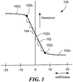
- a graph 100 has a horizontal axis with a scale in units of magnetic field in milliTesla (mT) and a vertical axis with a scale in units of resistance in arbitrary units.
- mT milliTesla
- a curve 102 is representative of a transfer function of an ideal GMR element, i.e., resistance versus magnetic field experienced by the GMR element.
- the transfer function 102 has a linear region 102a between an upper saturation point 102b and a lower saturation point 102c. Regions 102d, 102e are in saturation. It should be understood that the linear region 102a is an ideal linear region.
- an ideal GMR element presents the same value of resistance for a given field independent of its magnetic history, i.e., an ideal GMR element has no hysteresis.
- Steps are representative of an actual transfer function of the GMR element. Beyond the saturation points 102b, 102c, the actual transfer function represented by the steps 104 merges with the saturation regions 102d, 102e.
- the steps 104 are not desirable.
- the steps 104 result from magnetic behavior of magnetic domains within a so-called free layer in a GMR element. Behavior of the free layer is described more fully below in conjunction with FIG. 2 .
- steps 104 are shown to be regular steps with equal spacing and equal step heights, the steps 104 can also be irregular, with unequal spacing and unequal step heights (i.e., amplitudes).
- the steps usually correspond to local hysteretic and on reproducible local rotation of the free layer.
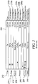
- a conventional prior art GMR element 200 includes a plurality of layers disposed over a substrate. An upper surface of the substrate is shown as a lowermost line at the bottom of FIG. 2 .
- each layer is identified by functional name.
- magnetic characteristics of sub-layers that can form the functional layers.
- magnetic materials can have a variety of magnetic characteristics and can be classified by a variety of terms, including, but not limited to, ferromagnetic, antiferromagnetic, and nonmagnetic. Description of the variety of types of magnetic materials is not made herein in detail. However, let it suffice here to say, that a ferromagnetic material is one in which magnetic moments of atoms within the ferromagnetic material tend to, on average, align to be both parallel and in the same direction, resulting in a nonzero net magnetic magnetization of the ferromagnetic material.
- Diamagnetic materials are also called nonmagnetic materials.
- An antiferromagnetic material is one in which magnetic moments within the antiferromagnetic material tend to, on average, align to be parallel, but in opposite directions in sub-layers within the antiferromagnetic material, resulting in a zero net magnetization.
- the conventional prior art GMR element 200 can include a seed layer 202 disposed over the substrate, an antiferromagnetic pinning layer 204 disposed over the seed layer 202, and a pinned layer structure 206 disposed over the antiferromagnetic pinning layer 204.
- the pinned layer structure 206 can be comprised of a first ferromagnetic pinned layer 206a, a second ferromagnetic pinned layer 206c, and a nonmagnetic spacer layer 206b disposed therebetween.
- the conventional GMR element 200 can also include a nonmagnetic spacer layer 208 disposed over the second ferromagnetic pinned layer 206c, and a free layer structure 210 disposed over the nonmagnetic spacer layer 208.
- the nonmagnetic spacer layer 206b can be a nonmagnetic metallic layer.
- the nonmagnetic spacer layer 208 can be metallic for GMR or insulating for TMR.
- the free layer structure 210 can be comprised of a first ferromagnetic free layer 210a and a second ferromagnetic free layer 210b.
- a cap layer 212 can be disposed over the free layer structure 210 to protect the GMR element 200.
- Examples of thicknesses of the layers of the conventional prior art GMR element 200 are shown in nanometers. Examples of materials of the layers of the conventional prior art GMR element are shown by atomic symbols.
- arrows are shown that are indicative or directions of magnetic field directions of the layers when the GMR element 200 does not experience an external magnetic field. Arrows coming out of the page are indicated as dots within circles and arrows going into the page are indicated as crosses within circles.
- the seed layer 202 is used to provide a regular crystalline structure upon the substrate that affects crystal properties of layers above, notably, the PtMn antiferromagnetic pinning layer 204 and layers above.
- sub-layers within the antiferromagnetic pinning layer 204 tend to have magnetic fields that point in alternating different directions indicated by right and left arrows, resulting in the antiferromagnetic pinning layer having a net magnetic field of zero.
- a top surface of the antiferromagnetic pinning layer 204 tends to have a magnetic moment pointing in one direction, here shown to the left.
- the first ferromagnetic pinned layer 206a tends to couple ferromagnetically to the top surface of the antiferromagnetic pinning layer 204, and thus, the magnetic field in the first ferromagnetic pinned layer 206a can be aligned in parallel to the magnetic moments at the top surface of the antiferromagnetic pinning layer 204, here shown to the left.
- the second ferromagnetic pinned layer 206c tends to couple antiferromagnetically with the first ferromagnetic pinned layer 206a, and thus, it has a magnetic field pointing in the other direction, here shown pointing to the right.
- the combination of the three layers 206a, 206b, 206c can be referred to as a synthetic antiferromagnetic structure or layer.
- the first and second free layers 210a, 210b have respective magnetic fields pointing out of the page in the absence of an external magnetic field.
- This pointing direction can be achieved by creating a specific anisotropy along a direction pointing out of the page. That anisotropy can be created by a shape of the GMR element or by other considerations described below in conjunction with FIG. 3 .
- the magnetic fields in the ferromagnetic free layers 210a, 210b tend to rotate to the right to become more aligned (or fully aligned, i.e., pointing to the right) with the magnetic field pointing direction in the second ferromagnetic pinned layer 206c.
- the magnetic fields in the pinned layer 206 are pinned by the antiferromagnetic pinning layer and do not rotate.
- the amount of rotation of the magnetic fields in the ferromagnetic free layers 210a, 210b depends upon the magnitude of the external magnetic field.
- the increased alignment of the magnetic fields in the ferromagnetic free layers 210a, 210b with the direction of the magnetic field in the second ferromagnetic pinned layer 206c tends to make a resistance of the GMR element 200 lower.
- the magnetic fields in the free layer structure 210 tend to rotate to the left to become more anti-aligned (or fully anti-aligned, i.e., pointing to the left) with the magnetic field pointing direction in the second ferromagnetic pinned layer 206c.
- the amount of rotation depends upon the magnitude of the external magnetic field.
- the increased anti-alignment of the magnetic fields in the ferromagnetic free layers 210a, 210b with the direction of the magnetic field in the second ferromagnetic pinned layer 206c tends to make a resistance of the GMR element 200 higher.
- a resistance of the GMR element 200 is at the center of the linear region 102a, and the resistance can move to the right or to the left on the transfer characteristic curve 102 (i.e., lower or higher) depending upon a direction of the external magnetic field 214.
- the GMR element 200 will be in the lower saturation region 102e or the upper saturation region 102d, respectively.
- the ferromagnetic free layers 210a, 210b tend to naturally have a plurality of magnetic domains, including, but not limited to, a first plurality of magnetic domains with magnetic fields pointing in a first direction and a second plurality of magnetic domains with magnetic fields pointing in one or more other directions.
- the first plurality of magnetic domains in the ferromagnetic free layers 210a, 210b have magnetic field pointing directions that are aligned with the net magnetic field of the free layer structure 210, shown to be coming out of the page when the GMR element 200 is not exposed to an external magnetic field, but which can rotate as the GMR element 200 is exposed to a magnetic field.
- the magnetic field pointing direction of the first plurality of magnetic domains rotates in response to the external magnetic field.
- the second plurality of magnetic domains tends to have magnetic field pointing directions that point in one or more other directions.
- each step is generated when one or more of the magnetic domains that are not within the first plurality of magnetic domains (e.g., that are within the second plurality of magnetic domains), i.e., one or more of the magnetic domains with magnetic fields not pointing in the direction of the net magnetic field in the ferromagnetic free layers 210a, 210b, suddenly snaps (i.e., jumps) in direction to become aligned with the net magnetic field pointing direction of the magnetic field in the ferromagnetic free layers 210a, 210b, wherever the net field in the ferromagnetic free layers 210a, 210b may be pointing (i.e., may have rotated) in response to an external magnetic field.
- one or more of the magnetic domains with magnetic fields not pointing in the direction of the net magnetic field in the ferromagnetic free layers 210a, 210b more slowly transitions in direction to become aligned with the net magnetic field pointing direction of the magnetic field in the ferromagnetic free layers 210a, 210b, in which case one or more of the steps of FIG. 1 would be less steep than those shown, but still undesirable.
- it would be desirable to reduce a number of magnetic domains in the free layer structure 210 that point in directions other than the direction of the net magnetic field in the free layer structure 210 i.e., reduce the quantity of magnetic domains within the second plurality of magnetic domains. This reduction would result in fewer steps 104, smaller steps 104, or no steps 104.
- an external biasing magnet can be used.
- a plurality of layers can be added to the basic GMR element 200 in order to achieve an intra-stack magnetic bias with a so-called "double pinned" arrangement.
- a material of the seed layer 202 can be manipulated to achieve an increased anisotropy in layers above.
- an example of a GMR element 300 includes a plurality of layers disposed over a substrate. An upper surface of the substrate is shown as a lowermost line at the bottom of FIG. 3 .
- each layer is identified by functional name.
- On the right side or FIG 3 are shown magnetic characteristics of sub-layers that can form the functional layers.
- the exemplary GMR element 300 can include a seed layer structure 302 disposed over the substrate.
- the seed layer structure 302 can be comprised of a first nonmagnetic spacer layer 302a, a ferromagnetic seed layer 302b disposed over the first nonmagnetic spacer layer 302a, and a second nonmagnetic spacer layer 302c disposed over the ferromagnetic seed layer 302b.
- the seed layer structure 302 is described more fully below.
- the seed layer structure 302 omits either the first nonmagnetic spacer layer 302a or the second nonmagnetic spacer layer 302c, but still includes the ferromagnetic seed layer 302b.
- the seed layer structure 302 includes only one nonmagnetic spacer layer, either above or below the ferromagnetic seed layer 302b.
- the nonmagnetic spacer layers 302a or 302c ensure proper crystalline growth of the ferromagnetic seed layer 302b and resulting anisotropy of the GMR element 300, in particular, anisotropy of a free layer structure described below.
- An antiferromagnetic pinning layer 304 can be disposed over the seed layer structure 302.
- the ferromagnetic seed layer 302b can have a crystalline axis with enhanced consistency, directionality, and definition by depositing the ferromagnetic seed layer 302b at a predetermined temperature (temperature) and predetermined vacuum in the presence of a predetermined magnetic field, the magnetic field having a static direction relative to the GMR element with a primary direction perpendicular to the magnetization of the antiferromagnetic pinning layer 304, which is also parallel to a surface of the substrate.
- the ferromagnetic seed layer 302b can be deposited without heating (e.g., at room temperature), at a base vacuum of about 1x10 -8 millibars, and in the presence of a magnetic field between about twenty Oersteds and one hundred fifty Oersteds.
- heating e.g., at room temperature
- base vacuum about 1x10 -8 millibars
- magnetic field between about twenty Oersteds and one hundred fifty Oersteds.
- other temperatures, vacuums, and magnetic fields may be possible.
- temperature can be in the range of about ten degrees Celsius to about fifty degrees Celsius
- vacuums can be in the range of about 1x10 -7 millibars to about 1x10 -10 millibars
- magnetic fields can be in the range of about ten to about five hundred Oersteds.
- only the ferromagnetic seed layer 302b is deposited under the above conditions. In some other embodiments, the entire seed layer structure 302 is deposited under the above conditions.
- a deposition machine by Singulus® Technologies AG of Germany performs layer deposition with linear translation rather than rotation.
- Linear translation deposition is well suited for application of a fixed direction magnetic field during deposition of the ferromagnetic seed layer 302b.
- the direction of the linear motion and the direction of the magnetic field applied during the deposition can be parallel to each other.
- Either the substrate or the deposition equipment, or both, can move with the linear translation.
- the ferromagnetic seed layer 302b has a crystalline anisotropy, the crystalline anisotropy induced by deposition of the ferromagnetic seed layer in the presence of the above described motion along a predetermined direction and in the presence of a predetermined magnetic field applied along the same predetermined direction, the crystalline anisotropy resulting in the free layer structure 310 having an enhanced preferential magnetic direction (e.g., an enhanced magnetic anisotropy).
- directions of magnetic fields in the antiferromagnetic pinning layer 304 and in the pinned layer structure 306 are the result of annealing at a predetermined temperature and with a predetermined magnetic field. The annealing is not described herein in detail.
- the GMR element 300 can have a rectangular shape.
- the direction of the magnetic field applied during deposition of the seed layer is along a long axis of the rectangle, which can also be the linear direction of travel of the wafer (or of the deposition equipment) during the deposition of the seed layer structure 302 (or of only the ferromagnetic seed layer 302b). Relative to the cross-sectional view of FIG. 3 and arrows shown thereon, the long axis of such a rectangle would come out of the page.
- the exemplary GMR element 300 can also include a pinned layer structure 306 disposed over the antiferromagnetic pinning layer 304.
- the pinned layer structure 306 can be comprised of a first ferromagnetic pinned layer 306a, a second ferromagnetic pinned layer 306c, and a nonmagnetic spacer layer 306b disposed there between.
- the GMR element 300 can also include a nonmagnetic spacer layer 308 disposed over the pinned layer 306, and a free layer structure 310 disposed over the nonmagnetic spacer layer 308.
- the free layer structure 310 can be comprised of a first ferromagnetic free layer 310a disposed under a second ferromagnetic free layer 310b.
- a cap layer 312 can be disposed at the top of the GMR element 300 to protect the GMR element 300.
- arrows are shown that are indicative or directions of magnetic fields of the layers when the GMR element 300 does not experience an external magnetic field. Arrows coming out of the page are indicated as dots within circles and arrows going into the page are indicated as crosses within circles.
- Thicknesses of the layers of the exemplary GMR element 300 are shown in nanometers. Materials of the layers of the exemplary GMR element 300 are shown by atomic symbols.
- the nonmagnetic seed layer 302a is comprised of Ru or Ta
- the ferromagnetic seed layer 302b is comprised of NiFe (or alternatively, NiFeCr, CoFe, CoFeB, or CoFeCr alloy)
- the first nonmagnetic spacer layer 302c is comprised of Ru or Ta
- the antiferromagnetic layer pinning 304 is comprised of PtMn
- the first pinned ferromagnetic layer 306a is comprised of CoFe
- the second nonmagnetic spacer layer 306b is comprised of Ru
- the second pinned ferromagnetic layer 306c is comprised of CoFe
- the third nonmagnetic spacer layer 308 is comprised of Cu (or alternatively, Au, or Ag)
- the first ferromagnetic free layer 310a is comprised of CoFe
- the second ferromagnetic free layer 310b is comprised of NiFe
- the cap layer 312 is comprised of Ta.
- the antiferromagnetic pinning layer 304 is comprised of IrMn, FeMn, or NiMn.
- the ferromagnetic seed layer 302b comprised of NiFe gives the GMR element 300 particular structural, and therefore, operational characteristics.
- NiFe or alternatively, NiFeCr, CoFe, CoFeB, or CoFeCr alloy
- the high crystallization of the ferromagnetic seed layer 302b propagates in subsequent layers to cause a high degree of crystallization in layers above the ferromagnetic seed layer 302b. In particular, this induces a preferential magnetic direction axis of the free layer structure 310.
- the seed layer structure 302 promotes a growth-induced anisotropy. Two directions along a magnetization axis become energetically favorable with respect to the all the other possible directions. As a consequence, there is a reduction in the number of magnetic domains in the free layer structure 310 that have magnetic fields pointing in directions other than the direction of the net magnetic field in the free layer structure 310.
- the free layer structure 310 tends to promote magnetic domains with magnetic fields oriented in a first direction and to reduce the number of magnetic domains with magnetic fields point in the above describe one or more second different directions.
- the promotion of the magnetic domains with fields pointing in the first direction i.e., aligned with the fields in the free layer structure 310 as the field in the free layer structure 310 rotates, tends to reduce the number of magnetic field domains with magnetic field pointing in the one or more second different other directions.
- This reduction results in fewer steps 104, smaller steps 104, or no steps 104.
- the reduction can include a reduction in a quantity of magnetic domains within the above second plurality of magnetic domains. Hysteresis can also be reduced.
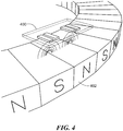
- a magnetic field sensor 400 can include one or more magnetoresistance elements.
- magnetoresistance elements which can be of a type described above in conjunction with FIG. 3 , are arranged over a common substrate.
- the four magnetoresistance elements can be arranged in a bridge.
- Other electronic components (not shown), for example, amplifiers and processors, can also be integrated upon the common substrate.
- the magnetic field sensor 400 can be disposed proximate to a moving magnetic object, for example, a ring magnet 402 having alternating north and south magnetic poles.
- the ring magnet 402 is subject to rotation.
- the magnetic field sensor 400 can be configured to generate an output signal indicative of at least a speed of rotation of the ring magnet.
- the ring magnet 402 is coupled to a target object, for example, a cam shaft in an engine, and the sensed speed of rotation of the ring magnet 402 is indicative of a speed of rotation of the target object.
- magnetic field sensor 400 is used as a rotation detector, it should be understood that other similar magnetic field sensors, for example, current sensors, can have one or more of the magnetoresistance elements of FIG. 3 .
- the seed layer structure 302 of FIG. 3 can be a seed layer structure in a double pinned arrangement or part of an arrangement with still further pinning and/or pinned layers.
Landscapes
- Physics & Mathematics (AREA)
- Engineering & Computer Science (AREA)
- Manufacturing & Machinery (AREA)
- Condensed Matter Physics & Semiconductors (AREA)
- General Physics & Mathematics (AREA)
- Crystallography & Structural Chemistry (AREA)
- Chemical & Material Sciences (AREA)
- Power Engineering (AREA)
- Nanotechnology (AREA)
- Spectroscopy & Molecular Physics (AREA)
- Hall/Mr Elements (AREA)
- Measuring Magnetic Variables (AREA)
- Thin Magnetic Films (AREA)
Description
- This invention relates generally to spin electronics magnetoresistance elements and, more particularly, to giant magnetoresistance (GMR) elements and tunnel magnetoresistance (TMR) elements that have an improved seed layer that promotes an improved response to magnetic fields.
- As used herein, the term "magnetic field sensing element" is used to describe a variety of electronic elements that can sense a magnetic field. One such magnetic field sensing element is a magnetoresistance (MR) element. The magnetoresistance element has a resistance that changes in relation to a magnetic field experienced by the magnetoresistance element.
- As is known, there are different types of magnetoresistance elements, for example, a semiconductor magnetoresistance element such as Indium Antimonide (InSb), an anisotropic magnetoresistance element (AMR), a giant magnetoresistance (GMR) element, and a tunneling magnetoresistance (TMR) element, also called a magnetic tunnel junction (MTJ) element. Some of the above magnetoresistance elements are sometimes referred to as spin valves.
- Of the above magnetoresistance elements, the GMR and the TMR elements operate with spin electronics (i.e., electron spins) where the resistance is related to the magnetic orientation of different magnetic layers separated by nonmagnetic layers. In spin valve configurations, the resistance is related to an angular direction of a magnetization in a so-called "free-layer" with respect to another layer, a so-called "reference layer." The free layer and the reference layer are described more fully below.
- The magnetoresistance element may be a single element or, alternatively, may include two or more magnetoresistance elements arranged in various configurations, e.g., a half bridge or full (Wheatstone) bridge.
- As used herein, the term "magnetic field sensor" is used to describe a circuit that uses a magnetic field sensing element, generally in combination with other circuits. In a typical magnetic field sensor, the magnetic field sensing element and the other circuits can be integrated upon a common substrate.
- Magnetic field sensors are used in a variety of applications, including, but not limited to, an angle sensor that senses an angle of a direction of a magnetic field, a current sensor that senses a magnetic field generated by a current carried by a current-carrying conductor, a magnetic switch that senses the proximity of a ferromagnetic object, a rotation detector that senses passing ferromagnetic articles, for example, magnetic domains of a ring magnet or a ferromagnetic target (e.g., gear teeth) where the magnetic field sensor is used in combination with a back-biased or other magnet, and a magnetic field sensor that senses a magnetic field density of a magnetic field.
- Various parameters characterize the performance of magnetic field sensors and magnetic field sensing elements. With regard to magnetic field sensing elements, the parameters include sensitivity, which is the change in the output signal of a magnetic field sensing element in response to a magnetic field, and linearity, which is the degree to which the output signal of a magnetic field sensor varies linearly (i.e., in direct proportion) to the magnetic field.
- GMR and TMR elements are known to have a relatively high sensitivity, compared, for example, to Hall elements. GMR and TMR elements are also known to have moderately good linearity, but over a restricted range of magnetic fields, more restricted in range than a range over which a Hall element can operate. However, it is known that even in the restricted range of magnetic fields, the linearity of the GMR or TMR element suffers from irregularities. Thus, it would be desirable to provide a GMR or a TMR element for which linearity irregularities are reduced.
- Conventional GMR and TMR elements, and, in particular, spin valves, are known to also have an undesirable hysteresis behaviour, which reduces their accuracy of magnetic field or current measurements. Thus, it would also be desirable to provide a GMR or TMR element with reduced hysteresis.
-
US 2006/193089 A1 discloses a giant magnetoresistance (GMR) sensor with strongly pinning and pinned layers for magnetic recording at ultrahigh densities. The pinning layer is an antiferromagnetic (AFM) iridium-manganese-chromium (Ir-Mn-Cr) film having a Mn content of approximately from 70 to 80 atomic percent and having a Cr content of approximately from 1 to 10 atomic percent. The first pinned layer is preferably a ferromagnetic Co-Fe having an Fe content of approximately from 20 to 80 at% and having high, positive saturation magnetostriction. The second pinned layer is preferably a ferromagnetic Co-Fe having an Fe content of approximately from 0 to 10 atomic percent.US 8422176 B1 discloses a method and system for providing a magnetic read transducer. The magnetic read transducer includes a bilayer magnetic seed layer, an AFM layer, and a read sensor. The bilayer magnetic seed layer includes a Ni1-xFex layer and a Ni1-yFey layer on the Ni1-xFex layer, where x is at least 0.3 and not more than 1 and where y is not more than 0.19. The AFM layer resides on the bilayer magnetic seed layer. The read sensor is on the AFM layer. -
US 2009/251829 A1 discloses a composite seed layer that reduces the shield to shield distance in a read head while improving Hex and Hex/Hc, and has a SM/A/SM/B configuration in which the SM layers are soft magnetic layers, the A layer is made of at least one of Co, Fe, Ni, and includes one or more amorphous elements, and the B layer is a buffer layer that contacts the AFM layer in the spin valve. The SM/A/SM stack together with the bottom (S1) shield forms an effective shield such that the buffer layer serves as the effective seed layer with a thickness as low as 5 Angstroms while maintaining a blocking temperature of 260°C in the AFM layer. -
US 2009/161268 A1 discloses a method, apparatus, and article of manufacture for a current-perpendicular-to-plane (CPP) GMR or a tunneling magnetoresistance (TMR) read sensor. The CPP read sensor comprises an amorphous ferromagnetic first seed layer, a polycrystalline nonmagnetic second seed layer, a nonmagnetic first cap layer, a nonmagnetic second cap layer, and a ferromagnetic third gap layer. A read gap is defined by a distance between the ferromagnetic first seed layer and the ferromagnetic third cap layer.US 6490140 B1 discloses a giant magnetoresistive stack for use in a magnetic read head, including a NiFeCr seed layer, a ferromagnetic free layer, at least one nonmagnetic spacer layer, at least one ferromagnetic pinned layer, and at least one PtMnX pinning layer, where X is selected from the group consisting of Cr, Pd, Nb, Re, Rh, Ta, Ru, Os, Zr, Hf, Ni, Co, and Fe. The ferromagnetic free layer has a rotatable magnetic moment. The ferromagnetic pinned layer has a fixed magnetic moment and is positioned adjacent to the PtMnX pinning layer. The nonmagnetic spacer layer is positioned between the free layer and the pinned layer. The NiFeCr seed layer is positioned adjacent to either the free layer or the pinning layer. -
US 2005/180059 A1 discloses a magnetic head having a free layer, an antiparallel (AP) pinned layer structure spaced apart from the free layer, and a high coercivity structure. The high coercivity structure pins a magnetic orientation of the AP pinned layer structure. The high coercivity structure includes a layer of high coercivity material, and an amorphous layer positioned between the high coercivity material and the AP pinned layer structure. -
US 2008/171223 A1 discloses a MTJ structure in which the seed layer is made of a lower Ta layer, a middle Hf layer, and an upper NiFe or NiFeX layer where X is Co, Cr, or Cu. Optionally, Zr, Cr, HfZr, or HfCr may be employed as the middle layer and materials having FCC structures such as CoFe and Cu may be used as the upper layer. As a result, the overlying layers in a TMR sensor will be smoother and less pin dispersion is observed. The Hex/Hc ratio is increased relative to that for a MTJ having a conventional Ta/Ru seed layer configuration. - DEVASAHAYAM A J ET AL, "Critical Thickness Effects of NiFeCr-CoFe Seed Layers for Spin Valve Multilayers", IEEE TRANSACTIONS ON MAGNETICS, IEEE SERVICE CENTER, NEW YORK, NY, US, vol. 40, no. 4, 1 July 2004, pages 2209-2211, discloses data on the critical dependence of the magnetic, electrical and microstructural properties of spin-valves (SV) on seed-layer thicknesses.
- SANKARANARAYANAN V K ET AL, "Exchange bias variations of the seed and top NiFe layers in NiFe/FeMn/NiFe trilayer as a function of seed layer thickness", JOURNAL OF MAGNETISM AND MAGNETIC MATERIALS, ELSEVIER SCIENCE PUBLISHERS, AMSTERDAM, NL, vol. 286, 1 February 2005, pages 196-199, investigates the development of exchange bias at the seed and top NiFe layers in the NiFe/FeMn/NiFe trilayer structure as a function of seed layer thickness, in the range of 2-20 nm.
- REPETSKI EDWARD J ET AL, "Improved interfaces and magnetic properties in spin valves using Ni80Fe20 seed layer", JOURNAL OF APPLIED PHYSICS, AMERICAN INSTITUTE OF PHYSICS, US, vol. 91, no. 6, 15 March 2002, pages 3891-3895, discusses GMR (Ni80Fe20)O-Co-Cu based "top" spin valves with and without Ni80Fe20 as a seed layer.
- The present invention provides a GMR or a TMR element (or any spin electronics magnetoresistance element) for which linearity irregularities are reduced, and for which hysteresis behavior is reduced. In particular, the present invention is directed to a MR element according to claim 1 and to a method of fabricating a MR element according to claim 18. Further embodiments of the invention are defined in the dependent claims.
- In accordance with an example useful for understanding an aspect of the present invention, a magnetoresistance element includes a substrate and a seed layer structure disposed over the substrate. The seed layer structure includes at least a ferromagnetic seed layer. The magnetoresistance element also includes a free layer structure disposed over the seed layer structure. The ferromagnetic seed layer comprises a crystalline anisotropy, the crystalline anisotropy induced by deposition of the ferromagnetic seed layer in the presence of a motion along a predetermined direction and in the presence of a predetermined magnetic field having the same predetermined direction, the crystalline anisotropy resulting in the free layer structure having an enhanced preferential magnetic direction.
- In some embodiments, the above magnetoresistance element can include one or more of the following aspects in any combination
- In some embodiments of the above magnetoresistance element, the seed layer structure further comprises a nonmagnetic spacer layer disposed over and proximate to or under and proximate to the ferromagnetic seed layer.
- In some embodiments of the above magnetoresistance element, the ferromagnetic seed layer is comprised of NiFe, NiFeCr, CoFe, CoFeB, or CoFeCr.
- In some embodiments of the above magnetoresistance element, the ferromagnetic seed layer is comprised of NiFe, NiFeCr, CoFe, CoFeB or CoFeCr.
- In some embodiments of the above magnetoresistance element, the predetermined magnetic field is between about twenty Oersteds and one hundred fifty Oersteds.
- In some embodiments of the above magnetoresistance element, the seed layer structure further comprises:
- a first nonmagnetic spacer layer disposed under and proximate to the ferromagnetic seed layer; and
- a second nonmagnetic spacer layer disposed over and proximate to the ferromagnetic seed layer.
- In some embodiments of the above magnetoresistance element, the first and second spacer layers are each comprised of Ru.
- In some embodiments of the above magnetoresistance element, the first and second spacer layers are each comprised of Ta.
- In some embodiments of the above magnetoresistance element, one of the first and second spacer layers is comprised of Ru and the other one of the first and second spacer layers is comprised of Ta.
- In some embodiments, the above magnetoresistance element further comprises:
an antiferromagnetic pinning layer disposed over the seed layer structure and under the free layer structure. - In some embodiments of the above magnetoresistance element, the antiferromagnetic pinning layer is comprised of PtMn.
- In some embodiments of the above magnetoresistance element, the antiferromagnetic pinning layer is comprised of PtMn, IrMn, or FeMn.
- In some embodiments, the above magnetoresistance element further comprises:
a pinned layer structure disposed over the antiferromagnetic pinning layer and under the free layer structure. - In some embodiments of the above magnetoresistance element, the pinned layer structure comprises:
- a first ferromagnetic pinned layer disposed over the antiferromagnetic pinning layer
- a third spacer layer disposed over the first pinned ferromagnetic layer; and
- a second ferromagnetic pinned layer disposed over the third spacer layer.
- In some embodiments of the above magnetoresistance element, the first and second ferromagnetic pinned layers are comprised of CoFe and the third spacer layer is comprised of Ru.
- In some embodiments, the above magnetoresistance element further comprises:
a fourth spacer layer disposed between the pinned layer structure and the free layer structure. - In some embodiments of the above magnetoresistance element, the fourth spacer layer is comprised of Cu, Au, or Ag.
- In some embodiments of the above magnetoresistance element, the free layer structure comprises:
- a first ferromagnetic free layer disposed over the fourth spacer layer; and
- a second ferromagnetic free layer disposed over the first ferromagnetic free layer.
- In some embodiments of the above magnetoresistance element, the first ferromagnetic free layer is comprise of CoFe and the second ferromagnetic free layer is comprised of NiFe.
- In some embodiments of the above magnetoresistance element, the free layer structure comprises a plurality of magnetic domains, the plurality of magnetic domains comprising:
- a first plurality of magnetic domains with magnetic fields pointing in a first direction; and
- a second plurality of magnetic domains with magnetic fields pointing in one or more directions different than the first direction, wherein the ferromagnetic seed layer is comprised of a selected material, the selected material resulting in a selected reduction in a quantity of magnetic domains within the second plurality of magnetic domains in the free layer structure.
- In some embodiments of the above magnetoresistance element, the ferromagnetic seed layer is comprised of NiFe, NiFeCr, CoFe or CoFeCr.
- In accordance with another example useful for understanding another aspect of the present invention, a method of fabricating a magnetoresistance element includes depositing a seed layer structure over a semiconductor substrate. The depositing the seed layer structure includes depositing at least a ferromagnetic seed layer over the substrate. The method further includes depositing a free layer structure over the seed layer structure, wherein the depositing the ferromagnetic seed layer comprises depositing the ferromagnetic seed layer in the presence of a motion along a predetermined direction and in the presence of a predetermined magnetic field having the same predetermined direction, resulting in the ferromagnetic seed layer having an enhanced crystalline anisotropy, and resulting in the free layer structure having an enhanced preferential magnetic direction.
- In some embodiments, the above method can include one or more of the following aspects in any combination.
- In some embodiments of the above method, the depositing the seed layer structure further comprises:
depositing a nonmagnetic spacer layer over and proximate to or under and proximate to the ferromagnetic spacer layer. - In some embodiments of the above method, the ferromagnetic seed layer is comprised of NiFe, NiFeCr, CoFe, CoFeB, or CoFeCr.
- In some embodiments of the above method, the ferromagnetic seed layer is comprised of NiFe, NiFeCr, CoFe, CoFeB, or CoFeCr.
- In some embodiments of the above method, the predetermined magnetic field is between about twenty Oersteds and one hundred fifty Oersteds.
- In some embodiments of the above method, the depositing the seed layer structure further comprises:
- depositing a first nonmagnetic spacer layer under and proximate to the ferromagnetic seed layer; and
- depositing a second nonmagnetic spacer layer over and proximate to the ferromagnetic seed layer.
- In some embodiments of the above method, the ferromagnetic seed layer is comprised of NiFe, NiFeCr, CoFe, CoFeB, or CoFeCr.
- In some embodiments of the above method, one of the first and second spacer layers is comprised of Ru and the other one of the first and second spacer layers is comprised of Ta, both the first and second spacer layers are comprised of Ru, or both the first and second spacer layers are comprise of Ta.
- In some embodiments, the above method further comprises:
- depositing an antiferromagnetic pinning layer over the seed layer structure; and
- annealing the antiferromagnetic pinning layer using an annealing magnetic field having a primary direction parallel to the predetermined direction of the predetermined magnetic field used in the depositing the ferromagnetic seed layer.
- In some embodiments of the above method, the ferromagnetic seed layer is comprised of NiFe, NiFeCr, CoFe, CoFeB, or CoFeCr.
- In some embodiments of the above method, the predetermined magnetic field is between about twenty Oersteds and one hundred fifty Oersteds.
- In some embodiments, the above method further comprises:
depositing a pinned layer structure between the antiferromagnetic pinning layer and the free layer structure. - In some embodiments of the above method, the ferromagnetic seed layer is comprised of NiFe, NiFeCr, CoFe, CoFeB, or CoFeCr.
- The foregoing features of the invention, as well as the invention itself may be more fully understood from the following detailed description of the drawings, in which:
-
FIG. 1 is a graph showing an ideal and an actual transfer characteristic of a giant magnetoresistance (GMR) element; -
FIG. 2 is a block diagram showing layers of a conventional prior art GMR element with a single pinned arrangement; -
FIG. 3 is a block diagram showing layers of another exemplary GMR element with a single pinned arrangement and having a particular seed layer; and -
FIG. 4 is a block diagram of a magnetoresistance element magnetic field sensor placed above a magnetic target for rotation speed measurement. - Before describing the present invention, it should be noted that reference is sometimes made herein to GMR or TMR elements having particular shapes (e.g., yoke shaped). One of ordinary skill in the art will appreciate, however, that the techniques described herein are applicable to a variety of sizes and shapes.
- As used herein, the term "anisotropy" or "anisotropic" refer to a particular axis or direction to which the magnetization of a ferromagnetic or ferrimagnetic layer tends to orientate when it does not experience an additional external field. An axial anisotropy can be created by a crystalline effect or by a shape anisotropy, both of which allow two equivalent directions of magnetic fields. A directional anisotropy can also be created in an adjacent layer, for example, by an antiferromagnetic layer, which allows only a single magnetic field direction along a specific axis in the adjacent layer.
- In view of the above, it will be understood that introduction of an anisotropy in a magnetic layer results in forcing the magnetization of the magnetic layer to be aligned along that anisotropy in the absence of an external field. In the case of a GMR or TMR element, a directional anisotropy provides an ability to obtain a coherent rotation of the magnetic field in a magnetic layer in response, for example, to an external magnetic field. Directional anisotropy also tends to suppress a hysteresis behavior of the corresponding element.
- As used herein, the term "magnetic field sensing element" is used to describe a variety of electronic elements that can sense a magnetic field. A magnetoresistance element is but one type of magnetic field sensing elements. Magnetoresistance elements include, but are not limited to, GMR and TMR elements, some of which can be spin valves.
- As used herein, the term "magnetic field sensor" is used to describe a circuit that uses a magnetic field sensing element, generally in combination with other circuits. Magnetic field sensors are used in a variety of applications, including, but not limited to, an angle sensor that senses an angle of a direction of a magnetic field, a current sensor that senses a magnetic field generated by a current carried by a current-carrying conductor, a magnetic switch that senses the proximity of a ferromagnetic object, a rotation detector that senses passing ferromagnetic articles, for example, magnetic domains of a ring magnet, and a magnetic field sensor that senses a magnetic field density of a magnetic field.
- Structures and methods described herein apply to both GMR and TMR magnetoresistance elements. However, it should be appreciated that the same or similar structures and methods can apply to other spin electronics magnetoresistance elements, either now known or later discovered. This includes, in particular, oxide based spin electronics structures.
- Referring now to
FIG. 1 , agraph 100 has a horizontal axis with a scale in units of magnetic field in milliTesla (mT) and a vertical axis with a scale in units of resistance in arbitrary units. - A
curve 102 is representative of a transfer function of an ideal GMR element, i.e., resistance versus magnetic field experienced by the GMR element. Thetransfer function 102 has alinear region 102a between an upper saturation point 102b and alower saturation point 102c.Regions linear region 102a is an ideal linear region. Furthermore, an ideal GMR element presents the same value of resistance for a given field independent of its magnetic history, i.e., an ideal GMR element has no hysteresis. - Steps, e.g., a
step 104, are representative of an actual transfer function of the GMR element. Beyond the saturation points 102b, 102c, the actual transfer function represented by thesteps 104 merges with thesaturation regions - The
steps 104 are not desirable. Thesteps 104 result from magnetic behavior of magnetic domains within a so-called free layer in a GMR element. Behavior of the free layer is described more fully below in conjunction withFIG. 2 . - While the
steps 104 are shown to be regular steps with equal spacing and equal step heights, thesteps 104 can also be irregular, with unequal spacing and unequal step heights (i.e., amplitudes). The steps usually correspond to local hysteretic and on reproducible local rotation of the free layer. - Referring now to
FIG. 2 , a conventional priorart GMR element 200 includes a plurality of layers disposed over a substrate. An upper surface of the substrate is shown as a lowermost line at the bottom ofFIG. 2 . - On the left side of
FIG. 2 , each layer is identified by functional name. On the right side orFIG. 2 are shown magnetic characteristics of sub-layers that can form the functional layers. In general, magnetic materials can have a variety of magnetic characteristics and can be classified by a variety of terms, including, but not limited to, ferromagnetic, antiferromagnetic, and nonmagnetic. Description of the variety of types of magnetic materials is not made herein in detail. However, let it suffice here to say, that a ferromagnetic material is one in which magnetic moments of atoms within the ferromagnetic material tend to, on average, align to be both parallel and in the same direction, resulting in a nonzero net magnetic magnetization of the ferromagnetic material. - Most materials like copper, silver, and gold are diamagnetic materials, which do not exhibit a net magnetization. These materials tend to present an extremely weak magnetization opposite and proportional to an applied (external) magnetic field. Diamagnetic materials are also called nonmagnetic materials.
- An antiferromagnetic material is one in which magnetic moments within the antiferromagnetic material tend to, on average, align to be parallel, but in opposite directions in sub-layers within the antiferromagnetic material, resulting in a zero net magnetization.
- As shown, the conventional prior
art GMR element 200 can include aseed layer 202 disposed over the substrate, an antiferromagnetic pinninglayer 204 disposed over theseed layer 202, and a pinnedlayer structure 206 disposed over the antiferromagnetic pinninglayer 204. The pinnedlayer structure 206 can be comprised of a first ferromagnetic pinnedlayer 206a, a second ferromagnetic pinnedlayer 206c, and anonmagnetic spacer layer 206b disposed therebetween. - The
conventional GMR element 200 can also include anonmagnetic spacer layer 208 disposed over the second ferromagnetic pinnedlayer 206c, and afree layer structure 210 disposed over thenonmagnetic spacer layer 208. Thenonmagnetic spacer layer 206b can be a nonmagnetic metallic layer. Thenonmagnetic spacer layer 208 can be metallic for GMR or insulating for TMR. Thefree layer structure 210 can be comprised of a first ferromagneticfree layer 210a and a second ferromagneticfree layer 210b. - A
cap layer 212 can be disposed over thefree layer structure 210 to protect theGMR element 200. - Examples of thicknesses of the layers of the conventional prior
art GMR element 200 are shown in nanometers. Examples of materials of the layers of the conventional prior art GMR element are shown by atomic symbols. - Within some layers, arrows are shown that are indicative or directions of magnetic field directions of the layers when the
GMR element 200 does not experience an external magnetic field. Arrows coming out of the page are indicated as dots within circles and arrows going into the page are indicated as crosses within circles. - Taking the layers from the bottom upward, the
seed layer 202 is used to provide a regular crystalline structure upon the substrate that affects crystal properties of layers above, notably, the PtMn antiferromagnetic pinninglayer 204 and layers above. - With regard to the antiferromagnetic pinning
layer 204, sub-layers (i.e., layer portions) within the antiferromagnetic pinninglayer 204 tend to have magnetic fields that point in alternating different directions indicated by right and left arrows, resulting in the antiferromagnetic pinning layer having a net magnetic field of zero. A top surface of the antiferromagnetic pinninglayer 204 tends to have a magnetic moment pointing in one direction, here shown to the left. - With regard to the pinned
layer 206, the first ferromagnetic pinnedlayer 206a tends to couple ferromagnetically to the top surface of the antiferromagnetic pinninglayer 204, and thus, the magnetic field in the first ferromagnetic pinnedlayer 206a can be aligned in parallel to the magnetic moments at the top surface of the antiferromagnetic pinninglayer 204, here shown to the left. - Due to the presence of the
spacer layer 206b between the first and second ferromagnetic pinnedlayers layer 206c tends to couple antiferromagnetically with the first ferromagnetic pinnedlayer 206a, and thus, it has a magnetic field pointing in the other direction, here shown pointing to the right. The combination of the threelayers - The first and second
free layers FIG. 3 . - In operation, when the
conventional GMR element 200 is exposed to an external magnetic field pointing in a direction of anarrow 214, the magnetic fields in the ferromagneticfree layers layer 206c. However, the magnetic fields in the pinnedlayer 206 are pinned by the antiferromagnetic pinning layer and do not rotate. The amount of rotation of the magnetic fields in the ferromagneticfree layers free layers layer 206c tends to make a resistance of theGMR element 200 lower. - Conversely, when the GMR element is exposed to an external field pointing opposite to the direction of the
arrow 214, the magnetic fields in thefree layer structure 210 tend to rotate to the left to become more anti-aligned (or fully anti-aligned, i.e., pointing to the left) with the magnetic field pointing direction in the second ferromagnetic pinnedlayer 206c. The amount of rotation depends upon the magnitude of the external magnetic field. The increased anti-alignment of the magnetic fields in the ferromagneticfree layers layer 206c tends to make a resistance of theGMR element 200 higher. - In view of the above, it will be understood that, referring briefly to
FIG. 1 , in the absence of an external magnetic field, a resistance of theGMR element 200 is at the center of thelinear region 102a, and the resistance can move to the right or to the left on the transfer characteristic curve 102 (i.e., lower or higher) depending upon a direction of the externalmagnetic field 214. When full alignment or full anti-alignment of layers is achieved, theGMR element 200 will be in thelower saturation region 102e or theupper saturation region 102d, respectively. - In general, the ferromagnetic
free layers free layers free layer structure 210, shown to be coming out of the page when theGMR element 200 is not exposed to an external magnetic field, but which can rotate as theGMR element 200 is exposed to a magnetic field. As described above, the magnetic field pointing direction of the first plurality of magnetic domains rotates in response to the external magnetic field. The second plurality of magnetic domains tends to have magnetic field pointing directions that point in one or more other directions. - Simply stated, with regard to the
steps 104 ofFIG. 1 , each step is generated when one or more of the magnetic domains that are not within the first plurality of magnetic domains (e.g., that are within the second plurality of magnetic domains), i.e., one or more of the magnetic domains with magnetic fields not pointing in the direction of the net magnetic field in the ferromagneticfree layers free layers free layers free layers free layers FIG. 1 would be less steep than those shown, but still undesirable. Thus, it would be desirable to reduce a number of magnetic domains in thefree layer structure 210 that point in directions other than the direction of the net magnetic field in the free layer structure 210 (i.e., reduce the quantity of magnetic domains within the second plurality of magnetic domains). This reduction would result infewer steps 104,smaller steps 104, or nosteps 104. - In order to reduce the number of magnetic domains in the
free layer 210 that point at directions other than the direction of the net magnetic field of the free layer, i.e., in order to reduce the number of magnetic domains that point in directions other than out of the page, an external biasing magnet can be used. As an alternative, a plurality of layers can be added to thebasic GMR element 200 in order to achieve an intra-stack magnetic bias with a so-called "double pinned" arrangement. As a further alternative, a material of theseed layer 202 can be manipulated to achieve an increased anisotropy in layers above. - Referring now to
FIG. 3 , an example of aGMR element 300 includes a plurality of layers disposed over a substrate. An upper surface of the substrate is shown as a lowermost line at the bottom ofFIG. 3 . - On the left side of
FIG. 3 , each layer is identified by functional name. On the right side orFIG 3 are shown magnetic characteristics of sub-layers that can form the functional layers. - As shown, the
exemplary GMR element 300 can include aseed layer structure 302 disposed over the substrate. Unlike theseed layer 202 ofFIG. 2 , theseed layer structure 302 can be comprised of a firstnonmagnetic spacer layer 302a, aferromagnetic seed layer 302b disposed over the firstnonmagnetic spacer layer 302a, and a secondnonmagnetic spacer layer 302c disposed over theferromagnetic seed layer 302b. Theseed layer structure 302 is described more fully below. - In other embodiments, the
seed layer structure 302 omits either the firstnonmagnetic spacer layer 302a or the secondnonmagnetic spacer layer 302c, but still includes theferromagnetic seed layer 302b. Thus, in the other embodiments, theseed layer structure 302 includes only one nonmagnetic spacer layer, either above or below theferromagnetic seed layer 302b. - In general, the
nonmagnetic spacer layers ferromagnetic seed layer 302b and resulting anisotropy of theGMR element 300, in particular, anisotropy of a free layer structure described below. - An antiferromagnetic pinning
layer 304 can be disposed over theseed layer structure 302. - The
ferromagnetic seed layer 302b can have a crystalline axis with enhanced consistency, directionality, and definition by depositing theferromagnetic seed layer 302b at a predetermined temperature (temperature) and predetermined vacuum in the presence of a predetermined magnetic field, the magnetic field having a static direction relative to the GMR element with a primary direction perpendicular to the magnetization of the antiferromagnetic pinninglayer 304, which is also parallel to a surface of the substrate. For example, theferromagnetic seed layer 302b can be deposited without heating (e.g., at room temperature), at a base vacuum of about 1x10⁻⁸ millibars, and in the presence of a magnetic field between about twenty Oersteds and one hundred fifty Oersteds. However, other temperatures, vacuums, and magnetic fields may be possible. - In some other embodiments, temperature can be in the range of about ten degrees Celsius to about fifty degrees Celsius, vacuums can be in the range of about 1x10⁻⁷ millibars to about 1x10⁻¹⁰ millibars, and magnetic fields can be in the range of about ten to about five hundred Oersteds.
- In some embodiments, only the
ferromagnetic seed layer 302b is deposited under the above conditions. In some other embodiments, the entireseed layer structure 302 is deposited under the above conditions. - A deposition machine by Singulus® Technologies AG of Germany performs layer deposition with linear translation rather than rotation. Linear translation deposition is well suited for application of a fixed direction magnetic field during deposition of the
ferromagnetic seed layer 302b. The direction of the linear motion and the direction of the magnetic field applied during the deposition can be parallel to each other. Either the substrate or the deposition equipment, or both, can move with the linear translation. However, it may also be possible to use a deposition machine that spins a wafer, and to provide a spinning magnetic field accordingly during deposition of theferromagnetic seed layer 302b. - From the above, it should be appreciated that the
ferromagnetic seed layer 302b has a crystalline anisotropy, the crystalline anisotropy induced by deposition of the ferromagnetic seed layer in the presence of the above described motion along a predetermined direction and in the presence of a predetermined magnetic field applied along the same predetermined direction, the crystalline anisotropy resulting in thefree layer structure 310 having an enhanced preferential magnetic direction (e.g., an enhanced magnetic anisotropy). - It will be understood that directions of magnetic fields in the antiferromagnetic pinning
layer 304 and in the pinnedlayer structure 306 are the result of annealing at a predetermined temperature and with a predetermined magnetic field. The annealing is not described herein in detail. - In a top view, in some embodiments, the
GMR element 300 can have a rectangular shape. - When fabricating a rectangular GMR element, the direction of the magnetic field applied during deposition of the seed layer is along a long axis of the rectangle, which can also be the linear direction of travel of the wafer (or of the deposition equipment) during the deposition of the seed layer structure 302 (or of only the
ferromagnetic seed layer 302b). Relative to the cross-sectional view ofFIG. 3 and arrows shown thereon, the long axis of such a rectangle would come out of the page. - The
exemplary GMR element 300 can also include a pinnedlayer structure 306 disposed over the antiferromagnetic pinninglayer 304. In some embodiments, the pinnedlayer structure 306 can be comprised of a first ferromagnetic pinnedlayer 306a, a second ferromagnetic pinnedlayer 306c, and anonmagnetic spacer layer 306b disposed there between. - The
GMR element 300 can also include anonmagnetic spacer layer 308 disposed over the pinnedlayer 306, and afree layer structure 310 disposed over thenonmagnetic spacer layer 308. In some embodiments, thefree layer structure 310 can be comprised of a first ferromagneticfree layer 310a disposed under a second ferromagneticfree layer 310b. - A
cap layer 312 can be disposed at the top of theGMR element 300 to protect theGMR element 300. - Within some layers, arrows are shown that are indicative or directions of magnetic fields of the layers when the
GMR element 300 does not experience an external magnetic field. Arrows coming out of the page are indicated as dots within circles and arrows going into the page are indicated as crosses within circles. - Thicknesses of the layers of the
exemplary GMR element 300 are shown in nanometers. Materials of the layers of theexemplary GMR element 300 are shown by atomic symbols. - Accordingly, in some embodiments, the
nonmagnetic seed layer 302a is comprised of Ru or Ta, theferromagnetic seed layer 302b is comprised of NiFe (or alternatively, NiFeCr, CoFe, CoFeB, or CoFeCr alloy), the firstnonmagnetic spacer layer 302c is comprised of Ru or Ta, the antiferromagnetic layer pinning 304 is comprised of PtMn, the first pinnedferromagnetic layer 306a is comprised of CoFe, the secondnonmagnetic spacer layer 306b is comprised of Ru, the second pinnedferromagnetic layer 306c is comprised of CoFe, the thirdnonmagnetic spacer layer 308 is comprised of Cu (or alternatively, Au, or Ag), the first ferromagneticfree layer 310a is comprised of CoFe, the second ferromagneticfree layer 310b is comprised of NiFe, and thecap layer 312 is comprised of Ta. However, other materials are also possible. - In some other embodiments, the antiferromagnetic pinning
layer 304 is comprised of IrMn, FeMn, or NiMn. - The
ferromagnetic seed layer 302b comprised of NiFe gives theGMR element 300 particular structural, and therefore, operational characteristics. In particular, by deposition techniques described above, it will be understood that NiFe (or alternatively, NiFeCr, CoFe, CoFeB, or CoFeCr alloy) has a crystalline axis with high degree of consistency, directionality, and definition, more than the crystallization of a conventional nonmagnetic seed layer, e.g., the conventional Ru orTa seed layer 202 ofFIG. 2 . The high crystallization of theferromagnetic seed layer 302b propagates in subsequent layers to cause a high degree of crystallization in layers above theferromagnetic seed layer 302b. In particular, this induces a preferential magnetic direction axis of thefree layer structure 310. - The
seed layer structure 302 promotes a growth-induced anisotropy. Two directions along a magnetization axis become energetically favorable with respect to the all the other possible directions. As a consequence, there is a reduction in the number of magnetic domains in thefree layer structure 310 that have magnetic fields pointing in directions other than the direction of the net magnetic field in thefree layer structure 310. - Having a higher degree of crystallization, the
free layer structure 310 tends to promote magnetic domains with magnetic fields oriented in a first direction and to reduce the number of magnetic domains with magnetic fields point in the above describe one or more second different directions. - Thus, with regard to the
steps 104 ofFIG. 1 , the promotion of the magnetic domains with fields pointing in the first direction, i.e., aligned with the fields in thefree layer structure 310 as the field in thefree layer structure 310 rotates, tends to reduce the number of magnetic field domains with magnetic field pointing in the one or more second different other directions. This reduction results infewer steps 104,smaller steps 104, or nosteps 104. The reduction can include a reduction in a quantity of magnetic domains within the above second plurality of magnetic domains. Hysteresis can also be reduced. - Referring now to
FIG. 4 , amagnetic field sensor 400 can include one or more magnetoresistance elements. Here, four magnetoresistance elements, which can be of a type described above in conjunction withFIG. 3 , are arranged over a common substrate. The four magnetoresistance elements can be arranged in a bridge. Other electronic components (not shown), for example, amplifiers and processors, can also be integrated upon the common substrate. - The
magnetic field sensor 400 can be disposed proximate to a moving magnetic object, for example, aring magnet 402 having alternating north and south magnetic poles. Thering magnet 402 is subject to rotation. - The
magnetic field sensor 400 can be configured to generate an output signal indicative of at least a speed of rotation of the ring magnet. In some arrangements, thering magnet 402 is coupled to a target object, for example, a cam shaft in an engine, and the sensed speed of rotation of thering magnet 402 is indicative of a speed of rotation of the target object. - While the
magnetic field sensor 400 is used as a rotation detector, it should be understood that other similar magnetic field sensors, for example, current sensors, can have one or more of the magnetoresistance elements ofFIG. 3 . - While a single pinned GMR element is described above in conjunction with
FIG. 3 , it should be understood that theseed layer structure 302 ofFIG. 3 can be a seed layer structure in a double pinned arrangement or part of an arrangement with still further pinning and/or pinned layers. - Examples of double pinned arrangements that can use the
seed layer 302 can be found, for example, isU.S. Patent Application No. 14/452,783, filed August 6, 2014 U.S. patent No. 14/529,564, filed October 31, 2014 - Having described preferred embodiments, which serve to illustrate various concepts, structures and techniques, which are the subject of this patent, it will now become apparent that other embodiments incorporating these concepts, structures and techniques may be used. Accordingly, it is submitted that that scope of the invention should not be limited to the described embodiments but rather should be limited only by the scope of the following claims.
Claims (24)
- A magnetoresistance element (300), comprising:a substrate;a seed layer structure (302) disposed over the substrate, the seed layer structure comprising:
a ferromagnetic seed layer (302b) consisting of a binary alloy of NiFe; and
a first nonmagnetic spacer layer (302a) disposed under and directly adjacent to the ferromagnetic seed layer and proximate to the substrate, wherein the first nonmagnetic spacer layer is comprised of Ta or Ru, the magnetoresistance element further comprising:a free layer structure (310) disposed over the seed layer structure, wherein the ferromagnetic seed layer (302b) comprises a crystalline anisotropy, the crystalline anisotropy being induced by deposition of the ferromagnetic seed layer in the presence of a motion along a predetermined direction and in the presence of a predetermined magnetic field having the same predetermined direction, the crystalline anisotropy being such that the free layer structure is promoted by the seed layer structure to have magnetic domains with magnetic fields oriented in a first direction and to reduce the number of domains with magnetic fields pointing in one or more second different directions. - The magnetoresistance element of Claim 1, wherein the seed layer structure further comprises a second nonmagnetic spacer layer (302c) disposed over and proximate to the ferromagnetic seed layer, wherein the second nonmagnetic spacer layer is comprised of Ta or Ru.
- The magnetoresistance element of Claim 1 or 2, wherein the predetermined magnetic field is between about twenty Oersteds and one hundred fifty Oersteds.
- The magnetoresistance element of Claim 2, wherein the first and second nonmagnetic spacer layers are each comprised of Ru.
- The magnetoresistance element of Claim 2, wherein the first and second nonmagnetic spacer layers are each comprised of Ta.
- The magnetoresistance element of Claim 2, wherein one of the first and second nonmagnetic spacer layers is comprised of Ru and the other one of the first and second nonmagnetic spacer layers is comprised of Ta.
- The magnetoresistance element of Claims 1 or 2, further comprising:an antiferromagnetic pinning layer (304) disposed over the seed layer structure and under the free layer structure.
- The magnetoresistance element of Claim 7, wherein the antiferromagnetic pinning layer is comprised of PtMn.
- The magnetoresistance element of Claim 7, wherein the antiferromagnetic pinning layer is comprised of PtMn, IrMn, or FeMn.
- The magnetoresistance element of Claim 7, further comprising:
a pinned layer structure (306) disposed over the antiferromagnetic pinning layer and under the free layer structure. - The magnetoresistance element of Claim 10, wherein the pinned layer structure comprises:a first ferromagnetic pinned layer (306a) disposed over the antiferromagnetic pinning layera third nonmagnetic spacer layer (306b) disposed over the first pinned ferromagnetic layer; anda second ferromagnetic pinned layer (306c) disposed over the third nonmagnetic spacer layer.
- The magnetoresistance element of Claim 11, wherein the first and second ferromagnetic pinned layers are comprised of CoFe and the third nonmagnetic spacer layer is comprised of Ru.
- The magnetoresistance element of Claim 10, further comprising:
a fourth nonmagnetic spacer layer (308) disposed between the pinned layer structure and the free layer structure. - The magnetoresistance element of Claim 13, wherein the fourth nonmagnetic spacer layer is comprised of Cu, Au, or Ag.
- The magnetoresistance element of Claim 13, wherein the free layer structure comprises:a first ferromagnetic free layer (310a) disposed over the fourth nonmagnetic spacer layer; anda second ferromagnetic free layer (310b) disposed over the first ferromagnetic free layer.
- The magnetoresistance element of Claim 15, wherein the first ferromagnetic free layer is comprise of CoFe and the second ferromagnetic free layer is comprised of NiFe.
- The magnetoresistance element of Claims 1 or 2, wherein the free layer structure comprises a plurality of magnetic domains, the plurality of magnetic domains comprising:a first plurality of magnetic domains with magnetic fields pointing in a first direction; anda second plurality of magnetic domains with magnetic fields pointing in one or more directions different than the first direction,wherein a material of the ferromagnetic seed layer results in a selected reduction in a quantity of magnetic domains within the second plurality of magnetic domains in the free layer structure.
- A method of fabricating a magnetoresistance element (300), comprising:depositing a seed layer structure (302) over a semiconductor substrate, wherein the depositing the seed layer structure comprises:depositing a ferromagnetic seed layer (302b) consisting of a binary alloy of NiFe; anddepositing a first nonmagnetic spacer layer (302a) disposed under and directly adjacent to the ferromagnetic seed layer and proximate to the substrate, wherein the first nonmagnetic spacer layer is comprised of Ta or Ru, wherein the method further comprises:depositing a free layer structure (310) over the seed layer structure, wherein the depositing the ferromagnetic seed layer comprises depositing the ferromagnetic seed layer in the presence of a motion along a predetermined direction and in the presence of a predetermined magnetic field having the same predetermined direction, resulting in the ferromagnetic seed layer having a greater crystalline anisotropy, and resulting in the free layer structure (310) having an enhanced preferential magnetic direction, such that the free layer structure is promoted by the seed layer structure to have magnetic domains with magnetic fields oriented in a first direction and to reduce the number of domains with magnetic fields pointing in one or more second different directions .
- The method of Claim 18, wherein the depositing the seed layer structure further comprises:
depositing a second nonmagnetic spacer layer (302c) over and proximate to the ferromagnetic seed layer, wherein the second nonmagnetic spacer layer is comprised of Ta or Ru. - The method of Claim 19, wherein one of the first and second nonmagnetic spacer layers is comprised of Ru and the other one of the first and second nonmagnetic spacer layers is comprised of Ta, both the first and second nonmagnetic spacer layers are comprised of Ru, or both the first and second nonmagnetic spacer layers are comprise of Ta.
- The method of Claim 18 or 19, further comprising:depositing an antiferromagnetic pinning layer (304) over the seed layer structure; andannealing the antiferromagnetic pinning layer using an annealing magnetic field having a primary direction parallel to the predetermined direction of the predetermined magnetic field used in the depositing the ferromagnetic seed layer.
- The method of Claim 18, 19 or 21, wherein the predetermined magnetic field is between about twenty Oersteds and one hundred fifty Oersteds.
- The method of Claim 21, further comprising:
depositing a pinned layer structure (306) between the antiferromagnetic pinning layer and the free layer structure. - The magnetoresistance element of Claims 1, 2 or 3, wherein the crystalline anisotropy is induced by deposition of the ferromagnetic seed layer in the presence of a motion along a predetermined direction and in the presence of a predetermined magnetic field having the same predetermined direction.
Applications Claiming Priority (2)
| Application Number | Priority Date | Filing Date | Title |
|---|---|---|---|
| US201461925446P | 2014-01-09 | 2014-01-09 | |
| PCT/US2015/010424 WO2015105836A1 (en) | 2014-01-09 | 2015-01-07 | Magnetoresistance element with an improved seed layer to promote an improved response to magnetic fields |
Publications (2)
| Publication Number | Publication Date |
|---|---|
| EP3092505A1 EP3092505A1 (en) | 2016-11-16 |
| EP3092505B1 true EP3092505B1 (en) | 2020-10-14 |
Family
ID=52394404
Family Applications (3)
| Application Number | Title | Priority Date | Filing Date |
|---|---|---|---|
| EP15701862.3A Active EP3090272B1 (en) | 2014-01-09 | 2015-01-07 | Magnetoresistance element with improved response to magnetic fields |
| EP15700938.2A Active EP3092505B1 (en) | 2014-01-09 | 2015-01-07 | Magnetoresistance element with an improved seed layer to promote an improved response to magnetic fields |
| EP15701863.1A Active EP3090273B1 (en) | 2014-01-09 | 2015-01-07 | Magnetoresistance element with improved response to magnetic fields |
Family Applications Before (1)
| Application Number | Title | Priority Date | Filing Date |
|---|---|---|---|
| EP15701862.3A Active EP3090272B1 (en) | 2014-01-09 | 2015-01-07 | Magnetoresistance element with improved response to magnetic fields |
Family Applications After (1)
| Application Number | Title | Priority Date | Filing Date |
|---|---|---|---|
| EP15701863.1A Active EP3090273B1 (en) | 2014-01-09 | 2015-01-07 | Magnetoresistance element with improved response to magnetic fields |
Country Status (5)
| Country | Link |
|---|---|
| US (4) | US9529060B2 (en) |
| EP (3) | EP3090272B1 (en) |
| JP (4) | JP6605478B2 (en) |
| KR (4) | KR102336037B1 (en) |
| WO (3) | WO2015105836A1 (en) |
Families Citing this family (39)
| Publication number | Priority date | Publication date | Assignee | Title |
|---|---|---|---|---|
| US9529060B2 (en) | 2014-01-09 | 2016-12-27 | Allegro Microsystems, Llc | Magnetoresistance element with improved response to magnetic fields |
| JP2015133377A (en) * | 2014-01-10 | 2015-07-23 | Tdk株式会社 | Magnetic detection element and rotation detection device |
| US9620707B2 (en) * | 2015-04-16 | 2017-04-11 | Infineon Technologies Ag | Magnetoresistive devices and methods for manufacturing magnetoresistive devices |
| JP6763887B2 (en) | 2015-06-05 | 2020-09-30 | アレグロ・マイクロシステムズ・エルエルシー | Spin valve magnetoresistive sensor with improved response to magnetic field |
| US10276787B2 (en) | 2016-02-11 | 2019-04-30 | Texas Instruments Incorporated | Integrated anisotropic magnetoresistive device |
| CN109314181B (en) * | 2016-06-20 | 2022-09-30 | 国立大学法人东北大学 | Tunnel magnetoresistive element and method for manufacturing the same |
| US9741372B1 (en) * | 2016-08-26 | 2017-08-22 | Allegro Microsystems, Llc | Double pinned magnetoresistance element with temporary ferromagnetic layer to improve annealing |
| US10620279B2 (en) | 2017-05-19 | 2020-04-14 | Allegro Microsystems, Llc | Magnetoresistance element with increased operational range |
| US11022661B2 (en) | 2017-05-19 | 2021-06-01 | Allegro Microsystems, Llc | Magnetoresistance element with increased operational range |
| FR3067116B1 (en) * | 2017-06-02 | 2019-07-12 | Commissariat A L'energie Atomique Et Aux Energies Alternatives | SYSTEM AND METHOD FOR LOW FREQUENCY NOISE REMOVAL OF MAGNETO-RESISTIVE MAGNETORESISTENCE TUNNEL SENSORS |
| US10365123B2 (en) * | 2017-07-21 | 2019-07-30 | Texas Instruments Incorporated | Anisotropic magneto-resistive (AMR) angle sensor |
| EP3442042B1 (en) * | 2017-08-10 | 2020-12-09 | Commissariat à l'Energie Atomique et aux Energies Alternatives | Synthetic antiferromagnetic layer, magnetic tunnel junction and spintronic device using said synthetic antiferromagnetic layer |
| JP2019068012A (en) | 2017-10-05 | 2019-04-25 | 東京エレクトロン株式会社 | Workpiece processing method |
| US20190178954A1 (en) * | 2017-12-11 | 2019-06-13 | Allegro Microsystems, Llc | Magnetoresistance Element Having Selected Characteristics To Achieve A Desired Linearity |
| US11199424B2 (en) | 2018-01-31 | 2021-12-14 | Allegro Microsystems, Llc | Reducing angle error in a magnetic field angle sensor |
| US10777345B2 (en) | 2018-02-21 | 2020-09-15 | Allegro Microsystems, Llc | Spin valve with bias alignment |
| US10840001B2 (en) | 2018-03-06 | 2020-11-17 | Allegro Microsystems, Llc | Magnetoresistance element with extended linear response to magnetic fields |
| US11193989B2 (en) | 2018-07-27 | 2021-12-07 | Allegro Microsystems, Llc | Magnetoresistance assembly having a TMR element disposed over or under a GMR element |
| US10605874B2 (en) | 2018-08-06 | 2020-03-31 | Allegro Microsystems, Llc | Magnetic field sensor with magnetoresistance elements having varying sensitivity |
| US10935612B2 (en) * | 2018-08-20 | 2021-03-02 | Allegro Microsystems, Llc | Current sensor having multiple sensitivity ranges |
| US10734443B2 (en) * | 2018-08-27 | 2020-08-04 | Allegro Microsystems, Llc | Dual manetoresistance element with two directions of response to external magnetic fields |
| US10753989B2 (en) | 2018-08-27 | 2020-08-25 | Allegro Microsystems, Llc | Magnetoresistance element with perpendicular or parallel magnetic anistropy |
| KR102262706B1 (en) * | 2019-07-30 | 2021-06-09 | 한양대학교 산학협력단 | Synthetic Antiferromagnetic Structure and Multi-Bit Memory using the same |
| US11209505B2 (en) * | 2019-08-26 | 2021-12-28 | Western Digital Technologies, Inc. | Large field range TMR sensor using free layer exchange pinning |
| US11175359B2 (en) | 2019-08-28 | 2021-11-16 | Allegro Microsystems, Llc | Reducing voltage non-linearity in a bridge having tunneling magnetoresistance (TMR) elements |
| US11127518B2 (en) | 2019-08-30 | 2021-09-21 | Allegro Microsystems, Llc | Tunnel magnetoresistance (TMR) element having cobalt iron and tantalum layers |
| US11217626B2 (en) | 2019-08-30 | 2022-01-04 | Allegro Microsystems, Llc | Dual tunnel magnetoresistance (TMR) element structure |
| FR3101156B1 (en) | 2019-09-19 | 2021-10-15 | Commissariat Energie Atomique | Magnetoresistive stack without radiated field, sensor and magnetic mapping system comprising such a stack |
| US11500042B2 (en) * | 2020-02-28 | 2022-11-15 | Brown University | Magnetic sensing devices based on interlayer exchange-coupled magnetic thin films |
| US11561112B2 (en) * | 2020-03-13 | 2023-01-24 | Allegro Microsystems, Llc | Current sensor having stray field immunity |
| US11467233B2 (en) | 2020-03-18 | 2022-10-11 | Allegro Microsystems, Llc | Linear bridges having nonlinear elements |
| US11408948B2 (en) | 2020-03-18 | 2022-08-09 | Allegro Microsystems, Llc | Linear bridge having nonlinear elements for operation in high magnetic field intensities |
| US11782103B2 (en) | 2020-06-12 | 2023-10-10 | Allegro Microsystems, Llc | Dual double-pinned spin valve element having magnet bias with increased linear range |
| US11630168B2 (en) | 2021-02-03 | 2023-04-18 | Allegro Microsystems, Llc | Linear sensor with dual spin valve element having reference layers with magnetization directions different from an external magnetic field direction |
| US11567108B2 (en) | 2021-03-31 | 2023-01-31 | Allegro Microsystems, Llc | Multi-gain channels for multi-range sensor |
| US11630169B1 (en) | 2022-01-17 | 2023-04-18 | Allegro Microsystems, Llc | Fabricating a coil above and below a magnetoresistance element |
| US11782105B2 (en) | 2022-01-17 | 2023-10-10 | Allegro Microsystems, Llc | Fabricating planarized coil layer in contact with magnetoresistance element |
| US11719771B1 (en) | 2022-06-02 | 2023-08-08 | Allegro Microsystems, Llc | Magnetoresistive sensor having seed layer hysteresis suppression |
| US20240094314A1 (en) * | 2022-09-15 | 2024-03-21 | Infineon Technologies Ag | Multiple cobalt iron boron layers in a free layer of a magnetoresistive sensing element |
Family Cites Families (202)
| Publication number | Priority date | Publication date | Assignee | Title |
|---|---|---|---|---|
| FR2665010B1 (en) | 1990-07-20 | 1992-09-18 | Thomson Csf | MAGNETIC READING DEVICE WITH MATRIX NETWORK OF READING HEADS. |
| DE4243358A1 (en) | 1992-12-21 | 1994-06-23 | Siemens Ag | Magnetic resistance sensor with artificial antiferromagnet and method for its production |
| FR2727778B1 (en) | 1994-12-02 | 1997-01-03 | Commissariat Energie Atomique | MAGNETIC ENCODER FOR READING MARKS ON AN ASSOCIATED MAGNETIC TRACK |
| FR2729790A1 (en) | 1995-01-24 | 1996-07-26 | Commissariat Energie Atomique | MAGNETORESISTANCE GEANTE, PROCESS FOR MANUFACTURING AND APPLICATION TO A MAGNETIC SENSOR |
| JPH09111419A (en) | 1995-10-16 | 1997-04-28 | Alps Electric Co Ltd | Magneto-resistance effect material and magnetro-resistance effect multilayer film |
| FR2742571B1 (en) | 1995-12-15 | 1998-01-16 | Commissariat Energie Atomique | MULTI-LAYERED STRUCTURE AND SENSOR AND METHOD FOR PRODUCING THE SAME |
| FR2752302B1 (en) | 1996-08-08 | 1998-09-11 | Commissariat Energie Atomique | MAGNETIC FIELD SENSOR WITH MAGNETORESISTANCE BRIDGE |
| US6026355A (en) | 1996-09-18 | 2000-02-15 | Itron, Inc. | Solid state watt-hour meter using GMR sensor |
| KR100521798B1 (en) | 1996-11-06 | 2006-01-12 | 가부시키가이샤 시마세이키 세이사쿠쇼 | Letter lowering device in flat knitting machine |
| JP3886589B2 (en) | 1997-03-07 | 2007-02-28 | アルプス電気株式会社 | Giant magnetoresistive element sensor |
| US5923514A (en) | 1997-11-05 | 1999-07-13 | Square D Company | Electronic trip circuit breaker with CMR current sensor |
| US5933308A (en) | 1997-11-19 | 1999-08-03 | Square D Company | Arcing fault protection system for a switchgear enclosure |
| FR2773395B1 (en) | 1998-01-05 | 2000-01-28 | Commissariat Energie Atomique | LINEAR ANGULAR SENSOR WITH MAGNETORESISTORS |
| US6094330A (en) | 1998-01-14 | 2000-07-25 | General Electric Company | Circuit interrupter having improved current sensing apparatus |
| US5933306A (en) | 1998-01-14 | 1999-08-03 | General Electric Company | Circuit breaker with ground fault detection module |
| FR2774774B1 (en) | 1998-02-11 | 2000-03-03 | Commissariat Energie Atomique | TUNNEL EFFECT MAGNETORESISTANCE AND MAGNETIC SENSOR USING SUCH A MAGNETORESISTANCE |
| US6141197A (en) | 1998-03-10 | 2000-10-31 | General Electric Company | Smart residential circuit breaker |
| DE19810838C2 (en) | 1998-03-12 | 2002-04-18 | Siemens Ag | Sensor device with at least one magnetoresistive sensor on a substrate layer of a sensor substrate |
| US6738236B1 (en) | 1998-05-07 | 2004-05-18 | Seagate Technology Llc | Spin valve/GMR sensor using synthetic antiferromagnetic layer pinned by Mn-alloy having a high blocking temperature |
| JP2000055997A (en) | 1998-08-05 | 2000-02-25 | Tdk Corp | Magnetic sensor device and current sensor device |
| JP2000056000A (en) | 1998-08-11 | 2000-02-25 | Tdk Corp | Magnetic sensor device and current sensor device |
| JP2000055999A (en) | 1998-08-11 | 2000-02-25 | Tdk Corp | Magnetic sensor device and current sensor device |
| DE19843348A1 (en) | 1998-09-22 | 2000-03-23 | Bosch Gmbh Robert | Magneto-resistive sensor element for measurement of external magnetic field angle, especially in automotive applications, has device for generating varying magnetic reference field in a reference magnetic layer |
| JP2002542617A (en) * | 1999-04-20 | 2002-12-10 | シーゲイト テクノロジー エルエルシー | Giant magnetoresistive sensor with Cr-Mn-Pt pinned layer and Ni-Fe-Cr seed layer |
| US6490140B1 (en) | 1999-04-28 | 2002-12-03 | Seagate Technology Llc | Giant magnetoresistive sensor with a PtMnX pinning layer and a NiFeCr seed layer |
| US6449134B1 (en) * | 1999-08-05 | 2002-09-10 | International Business Machines Corporation | Read head with file resettable dual spin valve sensor |
| US6278592B1 (en) * | 1999-08-17 | 2001-08-21 | Seagate Technology Llc | GMR spin valve having a bilayer TaN/NiFeCr seedlayer to improve GMR response and exchange pinning field |
| US6556390B1 (en) | 1999-10-28 | 2003-04-29 | Seagate Technology Llc | Spin valve sensors with an oxide layer utilizing electron specular scattering effect |
| US6411476B1 (en) * | 1999-10-28 | 2002-06-25 | International Business Machines Corporation | Trilayer seed layer structure for spin valve sensor |
| US6770382B1 (en) | 1999-11-22 | 2004-08-03 | Headway Technologies, Inc. | GMR configuration with enhanced spin filtering |
| US20010030839A1 (en) | 2000-01-13 | 2001-10-18 | Lieping Zhong | Dual spin-valve magnetoresistive sensor |
| JP4356172B2 (en) | 2000-02-16 | 2009-11-04 | ソニー株式会社 | Data transmission system and data distribution method |
| DE10009944A1 (en) | 2000-03-02 | 2001-09-13 | Forschungszentrum Juelich Gmbh | Arrangement for measuring magnetic field comprises first layer and second layer having electrically conducting antiferromagnetic layer bordering soft magnetic layer |
| US6504363B1 (en) | 2000-03-07 | 2003-01-07 | Teodor Dogaru | Sensor for eddy current testing and method of use thereof |
| WO2001067460A1 (en) * | 2000-03-09 | 2001-09-13 | Koninklijke Philips Electronics N.V. | Magnetic device with a coupling layer and method of manufacturing and operation of such device |
| US6549382B1 (en) * | 2000-06-14 | 2003-04-15 | International Business Machines Corporation | Read head with asymmetric dual AP pinned spin valve sensor |
| JP2002082136A (en) | 2000-06-23 | 2002-03-22 | Yazaki Corp | Current sensor |
| US6429640B1 (en) | 2000-08-21 | 2002-08-06 | The United States Of America As Represented By The Secretary Of The Air Force | GMR high current, wide dynamic range sensor |
| US6521098B1 (en) * | 2000-08-31 | 2003-02-18 | International Business Machines Corporation | Fabrication method for spin valve sensor with insulating and conducting seed layers |
| JP3603771B2 (en) * | 2000-09-26 | 2004-12-22 | 松下電器産業株式会社 | Magnetic resistance element, magnetic sensor and memory device using the same |
| FR2814592B1 (en) | 2000-09-26 | 2003-01-03 | Commissariat Energie Atomique | SPIN VALVE DEVICE WITH SPECULAR ELECTRONIC REFLECTION DEPENDENT OF SPIN |
| JP2002150511A (en) | 2000-11-06 | 2002-05-24 | Fujitsu Ltd | Spin valve magnetoresistive element and magnetic head using the same |
| US6992482B2 (en) | 2000-11-08 | 2006-01-31 | Jentek Sensors, Inc. | Magnetic field sensor having a switchable drive current spatial distribution |
| FR2817998B1 (en) | 2000-12-07 | 2003-01-10 | Commissariat Energie Atomique | SPIN POLARIZATION MAGNETIC DEVICE WITH MAGNIFICATION ROTATION, MEMORY AND WRITING METHOD USING THE DEVICE |
| FR2817999B1 (en) | 2000-12-07 | 2003-01-10 | Commissariat Energie Atomique | MAGNETIC DEVICE WITH POLARIZATION OF SPIN AND A STRIP (S) TRI-LAYER (S) AND MEMORY USING THE DEVICE |
| JP2002207692A (en) | 2001-01-12 | 2002-07-26 | Ricoh Co Ltd | Picture data transferring device, printer and picture data transferring system |
| JP2004022614A (en) * | 2002-06-13 | 2004-01-22 | Alps Electric Co Ltd | Magnetic sensor element and method of manufacturing the same |
| JP2002314164A (en) * | 2001-02-06 | 2002-10-25 | Sony Corp | Magnetic tunnel element and its manufacturing method, thin film magnetic head, magnetic memory and magnetic sensor |
| US7050275B2 (en) * | 2001-02-20 | 2006-05-23 | Alps Electric Co., Ltd. | Exchange coupled film having improved current-carrying reliability and improved rate of change in resistance and magnetic sensing element using same |
| JP2002267692A (en) | 2001-03-08 | 2002-09-18 | Yazaki Corp | Current sensor |
| JP2004523928A (en) | 2001-04-12 | 2004-08-05 | ライプニッツ−インスティトゥート フュア フェストケルパー− ウント ヴェルクシュトフフォルシュング ドレスデン エー ファオ | Method for determining reference magnetization in layered systems |
| JP2002328140A (en) | 2001-04-27 | 2002-11-15 | Yazaki Corp | Current sensor |
| US6791805B2 (en) | 2001-05-03 | 2004-09-14 | Seagate Technology Llc | Current-perpendicular-to-plane spin valve reader with reduced scattering of majority spin electrons |
| EP1260787A1 (en) | 2001-05-21 | 2002-11-27 | ruf electronics gmbh | Angle sensor with magnetoresistive sensing elements |
| JP3563375B2 (en) * | 2001-06-19 | 2004-09-08 | アルプス電気株式会社 | Magnetic detecting element and thin-film magnetic head using the magnetic detecting element |
| US6709767B2 (en) | 2001-07-31 | 2004-03-23 | Hitachi Global Storage Technologies Netherlands B.V. | In-situ oxidized films for use as cap and gap layers in a spin-valve sensor and methods of manufacture |
| US6600638B2 (en) * | 2001-09-17 | 2003-07-29 | International Business Machines Corporation | Corrosion resistive GMR and MTJ sensors |
| US6888703B2 (en) | 2001-09-17 | 2005-05-03 | Headway Technologies, Inc. | Multilayered structures comprising magnetic nano-oxide layers for current perpindicular to plane GMR heads |
| JP3973442B2 (en) * | 2001-09-25 | 2007-09-12 | アルプス電気株式会社 | Magnetic sensing element and manufacturing method thereof |
| FR2830621B1 (en) | 2001-10-09 | 2004-05-28 | Commissariat Energie Atomique | STRUCTURE FOR SENSOR AND MAGNETIC FIELD SENSOR |
| FR2830971B1 (en) | 2001-10-12 | 2004-03-12 | Commissariat Energie Atomique | MAGNETORESISTIVE DEVICE WITH IMPROVED PERFORMANCE SPIN VALVE |
| JP3839697B2 (en) | 2001-10-17 | 2006-11-01 | アルプス電気株式会社 | Rotation angle sensor |
| JP3799270B2 (en) | 2001-12-21 | 2006-07-19 | 株式会社日立製作所 | Control device for switching the driving state of an automobile |
| JP3793725B2 (en) * | 2002-01-25 | 2006-07-05 | アルプス電気株式会社 | Magnetic detection element, method of manufacturing the same, and magnetic detection apparatus using the magnetic detection element |
| EP1336985A1 (en) | 2002-02-19 | 2003-08-20 | Singulus Technologies AG | Sputtering cathode, and device and method for coating a substrate with a plurality of layers |
| US7161771B2 (en) | 2002-04-02 | 2007-01-09 | Hitachi Global Storage Technologies Netherlands B.V. | Dual spin valve sensor with a longitudinal bias stack |
| JP4663204B2 (en) | 2002-04-17 | 2011-04-06 | 財団法人電気磁気材料研究所 | Rotation angle sensor |
| JP3660323B2 (en) | 2002-04-25 | 2005-06-15 | 久保木 襄 | Fish breeding tanks such as saltwater fish |
| US20040056654A1 (en) | 2002-05-21 | 2004-03-25 | Jentek Sensors, Inc. | Magnetic field characterization of stresses and properties in materials |
| DE10222467A1 (en) | 2002-05-22 | 2003-12-11 | A B Elektronik Gmbh | Giant magnetic resistor sensor for contactless detection of rotary/linear motion of relatively movable parts has stationary part with GMR cell of variable GMR resistance, magnet element rotary part |
| US6927566B2 (en) | 2002-05-22 | 2005-08-09 | Ab Eletronik Gmbh | Device for generating output voltages |
| KR20050012774A (en) | 2002-06-06 | 2005-02-02 | 코닌클리즈케 필립스 일렉트로닉스 엔.브이. | Sensor and method for measuring a current of charged particles |
| EP1525443A4 (en) | 2002-06-07 | 2007-08-01 | Automotive Systems Lab | Seat belt tension sensor |
| US7106046B2 (en) | 2002-06-18 | 2006-09-12 | Asahi Kasei Emd Corporation | Current measuring method and current measuring device |
| US20030235016A1 (en) * | 2002-06-19 | 2003-12-25 | International Business Machines Corporation | Stabilization structures for CPP sensor |
| JP2004031545A (en) * | 2002-06-25 | 2004-01-29 | Alps Electric Co Ltd | Magnetic detector and its manufacturing method |
| US6831816B2 (en) | 2002-07-15 | 2004-12-14 | International Business Machines Corporation | CPP sensor with in-stack biased free layer |
| DE10257253A1 (en) | 2002-07-26 | 2004-02-05 | Robert Bosch Gmbh | Giant magnetoresistive sensor for motor vehicle cam and crank shafts has eight magnetoresistive elements in two Wheatstone bridges |
| US6781359B2 (en) | 2002-09-20 | 2004-08-24 | Allegro Microsystems, Inc. | Integrated current sensor |
| DE10255327A1 (en) | 2002-11-27 | 2004-06-24 | Robert Bosch Gmbh | Magnetoresistive sensor element and method for reducing the angular error of a magnetoresistive sensor element |
| JP4302063B2 (en) | 2003-01-31 | 2009-07-22 | コミサリア、ア、レネルジ、アトミク | Magnetic field sensing device |
| WO2004068152A1 (en) | 2003-01-31 | 2004-08-12 | Commissariat Energie Atomique | Device for sensing rf field |
| US7239000B2 (en) | 2003-04-15 | 2007-07-03 | Honeywell International Inc. | Semiconductor device and magneto-resistive sensor integration |
| JP2005018908A (en) * | 2003-06-26 | 2005-01-20 | Tdk Corp | Magnetoresistive effect device and its manufacturing method, thin film magnetic head, head gimbal assembly, and hard disk device |
| JP4259937B2 (en) | 2003-06-30 | 2009-04-30 | アルプス電気株式会社 | Angle detection sensor |
| US6985385B2 (en) | 2003-08-26 | 2006-01-10 | Grandis, Inc. | Magnetic memory element utilizing spin transfer switching and storing multiple bits |
| DE10340065A1 (en) | 2003-08-28 | 2005-04-07 | Lenord, Bauer & Co. Gmbh | Method and angle encoder for measuring the absolute angular position |
| JP2005091137A (en) | 2003-09-17 | 2005-04-07 | Nsk Ltd | Rudder angle sensor |
| JP2005209301A (en) * | 2004-01-23 | 2005-08-04 | Hitachi Global Storage Technologies Netherlands Bv | Magnetic head and its manufacturing method |
| US7221545B2 (en) | 2004-02-18 | 2007-05-22 | Hitachi Global Storage Technologies Netherlands B.V. | High HC reference layer structure for self-pinned GMR heads |
| US20110140217A1 (en) | 2004-02-26 | 2011-06-16 | Grandis, Inc. | Spin transfer magnetic element with free layers having high perpendicular anisotropy and in-plane equilibrium magnetization |
| US6992359B2 (en) * | 2004-02-26 | 2006-01-31 | Grandis, Inc. | Spin transfer magnetic element with free layers having high perpendicular anisotropy and in-plane equilibrium magnetization |
| US7180716B2 (en) * | 2004-03-30 | 2007-02-20 | Headway Technologies, Inc. | Fabrication method for an in-stack stabilized synthetic stitched CPP GMR head |
| US7611912B2 (en) * | 2004-06-30 | 2009-11-03 | Headway Technologies, Inc. | Underlayer for high performance magnetic tunneling junction MRAM |
| EP1617472A1 (en) | 2004-07-16 | 2006-01-18 | Axalto SA | An active protection device for protecting a circuit against mechanical and electromagnetic attack |
| US7377557B2 (en) | 2004-08-20 | 2008-05-27 | Honeywell International Inc. | Scissor mechanism for a latch assembly |
| US7397637B2 (en) | 2004-08-30 | 2008-07-08 | Hitachi Global Storage Technologies Netherlands B.V. | Sensor with in-stack bias structure providing enhanced magnetostatic stabilization |
| US7324312B2 (en) * | 2004-08-30 | 2008-01-29 | Hitachi Global Storage Technologies Netherlands B.V. | Sensor with in-stack bias structure providing exchange stabilization |
| US7324313B2 (en) * | 2004-09-30 | 2008-01-29 | Hitachi Global Storage Technologies Netherlands B.V. | Read sensor having an in-stack biasing structure and an AP coupled free layer structure for increased magnetic stability |
| US7777607B2 (en) | 2004-10-12 | 2010-08-17 | Allegro Microsystems, Inc. | Resistor having a predetermined temperature coefficient |
| FR2876800B1 (en) | 2004-10-18 | 2007-03-02 | Commissariat Energie Atomique | METHOD AND DEVICE FOR MEASURING A MAGNETIC FIELD USING A MAGNETORESITIVE SENSOR |
| JP4105142B2 (en) | 2004-10-28 | 2008-06-25 | Tdk株式会社 | Current sensor |
| JP4105145B2 (en) | 2004-11-30 | 2008-06-25 | Tdk株式会社 | Current sensor |
| JP4105147B2 (en) | 2004-12-06 | 2008-06-25 | Tdk株式会社 | Current sensor |
| JP4689435B2 (en) | 2004-12-16 | 2011-05-25 | アルプス電気株式会社 | Angle detection sensor |
| JP2006179566A (en) * | 2004-12-21 | 2006-07-06 | Tdk Corp | Magnetoresistive effect element, thin film magnetic head equipped therewith, head gimbals assembly equipped with thin film magnetic head, magnetic disc device equipped with head gimbals assembly, and method of manufacturing magnetoresistive effect element |
| US7639459B2 (en) | 2005-01-10 | 2009-12-29 | Hitachi Global Storage Technologies Netherlands B.V. | Three terminal magnetic sensor having an in-stack longitudinal biasing layer structure |
| US7342753B2 (en) | 2005-01-20 | 2008-03-11 | Hitachi Global Storage Technologies Netherlands B.V. | In-stack biasing of the free layer of a magnetoresistive read element |
| JP2006214091A (en) | 2005-02-01 | 2006-08-17 | Aisin Keikinzoku Co Ltd | Waterproof structure of skylight |
| JP4411223B2 (en) | 2005-02-04 | 2010-02-10 | アルプス電気株式会社 | In-vehicle GMR angle sensor |
| US7554775B2 (en) | 2005-02-28 | 2009-06-30 | Hitachi Global Storage Technologies Netherlands B.V. | GMR sensors with strongly pinning and pinned layers |
| US7453720B2 (en) | 2005-05-26 | 2008-11-18 | Maglabs, Inc. | Magnetic random access memory with stacked toggle memory cells having oppositely-directed easy-axis biasing |
| DE102005024879B4 (en) | 2005-05-31 | 2018-12-06 | Infineon Technologies Ag | A method for determining residual error compensation parameters for a magnetoresistive angle sensor and method for reducing a residual angle error in a magnetoresistive angle sensor |
| DE102006021774B4 (en) | 2005-06-23 | 2014-04-03 | Siemens Aktiengesellschaft | Current sensor for galvanically isolated current measurement |
| US7411765B2 (en) | 2005-07-18 | 2008-08-12 | Hitachi Global Storage Technologies Netherlands B.V. | CPP-GMR sensor with non-orthogonal free and reference layer magnetization orientation |
| JP4088641B2 (en) | 2005-07-22 | 2008-05-21 | Tdk株式会社 | Magnetoresistive element, thin film magnetic head, head gimbal assembly, head arm assembly, magnetic disk drive, magnetic memory cell and current sensor |
| FR2889348B1 (en) | 2005-07-27 | 2008-09-12 | Commissariat Energie Atomique | MAGNETORESISTIVE DEVICE |
| JP2007064851A (en) | 2005-08-31 | 2007-03-15 | Tdk Corp | Coil, coil module, their manufacturing method, current sensor and its manufacturing method |
| DE102005042307A1 (en) | 2005-09-06 | 2007-03-08 | Trw Automotive Gmbh | Safety belt retractor for motor vehicle, has measuring unit with giant magneto-resistive-sensor that is designed as swiveling angle sensor and permanent magnets effecting relative movement to sensor during rotation of belt spool |
| US7423849B2 (en) | 2005-09-19 | 2008-09-09 | Hitachi Global Sotrage Technologies Netherlands B.V. | Magnetoresistive (MR) elements having pinned layers with canted magnetic moments |
| US7973349B2 (en) | 2005-09-20 | 2011-07-05 | Grandis Inc. | Magnetic device having multilayered free ferromagnetic layer |
| JP4415923B2 (en) | 2005-09-30 | 2010-02-17 | Tdk株式会社 | Current sensor |
| JP4298691B2 (en) | 2005-09-30 | 2009-07-22 | Tdk株式会社 | Current sensor and manufacturing method thereof |
| JP4224483B2 (en) | 2005-10-14 | 2009-02-12 | Tdk株式会社 | Current sensor |
| JP4739963B2 (en) | 2006-01-18 | 2011-08-03 | アルプス電気株式会社 | In-vehicle GMR angle sensor |
| EP1991862B1 (en) * | 2006-02-24 | 2013-07-10 | Commissariat à l'Énergie Atomique et aux Énergies Alternatives | Method and device for non destructive evaluation of defects in a metallic object |
| JP2007273504A (en) | 2006-03-30 | 2007-10-18 | Fujitsu Ltd | Magnetoresistive effect element, magnetic head, magnetic recorder, magnetic random access memory |
| US7633724B2 (en) | 2006-03-31 | 2009-12-15 | Hitachi Global Storage Technologies Netherlands, B.V. | Dual-type tunneling magnetoresistance (TMR) elements |
| DE102006019483A1 (en) | 2006-04-26 | 2007-10-31 | Siemens Ag | Organo-magneto-resistive sensor arrangement for e.g. position measurement, has electronic thin layer component, where arrangement is formed in such a manner that field generating device causes magneto-resistive change in layer component |
| FR2902890B1 (en) | 2006-06-22 | 2008-11-07 | Commissariat Energie Atomique | METHOD AND SYSTEM FOR ADJUSTING THE SENSITIVITY OF A MAGNETORESISTIVE SENSOR |
| FR2902891B1 (en) | 2006-06-22 | 2008-12-12 | Commissariat Energie Atomique | SYSTEM AND METHOD FOR MEASURING A MAGNETIC RESONANCE SIGNAL |
| DE102006034579A1 (en) | 2006-07-26 | 2008-01-31 | Siemens Ag | Current detection device and method for current detection |
| FR2904724B1 (en) | 2006-08-03 | 2011-03-04 | Commissariat Energie Atomique | MAGNETIC DEVICE IN THIN LAYERS WITH HIGH PERPENDICULAR SPIN POLARIZATION IN THE LAYER PLAN, MAGNETIC TUNNEL JUNCTION AND SPIN VALVE USING SUCH A DEVICE |
| FR2907587B1 (en) | 2006-10-23 | 2008-12-26 | Commissariat Energie Atomique | MAGNETIC DEVICE WITH PERPENDICULAR ANIMATION AND INTERCOUNTING COMPENSATORY INTERCONNECTIVE LAYER. |
| JP4991322B2 (en) | 2006-10-30 | 2012-08-01 | 日立オートモティブシステムズ株式会社 | Displacement sensor using GMR element, angle detection sensor using GMR element, and semiconductor device used therefor |
| FR2910716B1 (en) | 2006-12-26 | 2010-03-26 | Commissariat Energie Atomique | MULTILAYER MAGNETIC DEVICE, METHOD FOR PRODUCING THE SAME, MAGNETIC FIELD SENSOR, MAGNETIC MEMORY AND LOGIC HOLDER USING SUCH A DEVICE |
| US7476954B2 (en) * | 2007-01-12 | 2009-01-13 | Headway Technologies, Inc. | TMR device with Hf based seed layer |
| FR2911690B1 (en) | 2007-01-19 | 2009-03-06 | Thales Sa | MAGNETIC AMPLIFICATION DEVICE COMPRISING A MAGNETIC SENSOR WITH LONGITUDINAL SENSITIVITY |
| EP1990414A1 (en) | 2007-05-10 | 2008-11-12 | Fraunhofer-Gesellschaft zur Förderung der angewandten Forschung e.V. | Means for treating inflammatory diseases, autoimmune diseases and cancer |
| JP4877095B2 (en) | 2007-06-25 | 2012-02-15 | Tdk株式会社 | Current sensor and manufacturing method thereof |
| JP5362713B2 (en) | 2007-06-27 | 2013-12-11 | コミサリア ア レネルジ アトミク | Low frequency noise removal method in magnetoresistive composite sensor |
| ATE507485T1 (en) | 2007-06-27 | 2011-05-15 | Commissariat Energie Atomique | DEVICE BASED ON A MAGNETORESISTIVE MIXED SENSOR WITHOUT LOW FREQUENCY NOISE AND RELATED METHOD |
| JP4979487B2 (en) | 2007-07-05 | 2012-07-18 | アルプス電気株式会社 | Angle sensor |
| FR2918761B1 (en) | 2007-07-10 | 2009-11-06 | Commissariat Energie Atomique | MAGNETIC FIELD SENSOR WITH LOW NOISE. |
| FR2918762B1 (en) | 2007-07-10 | 2010-03-19 | Commissariat Energie Atomique | LOW NOISE MAGNETIC FIELD SENSOR USING LATERAL SPIN TRANSFER. |
| US7583073B2 (en) | 2007-07-19 | 2009-09-01 | Honeywell International Inc. | Core-less current sensor |
| US7394247B1 (en) | 2007-07-26 | 2008-07-01 | Magic Technologies, Inc. | Magnetic field angle sensor with GMR or MTJ elements |
| US8715776B2 (en) | 2007-09-28 | 2014-05-06 | Headway Technologies, Inc. | Method for providing AFM exchange pinning fields in multiple directions on same substrate |
| US20090115405A1 (en) | 2007-11-01 | 2009-05-07 | Magic Technologies, Inc. | Magnetic field angular sensor with a full angle detection |
| US20090161268A1 (en) | 2007-12-22 | 2009-06-25 | Tsann Lin | Current-perpendicular-to-plane read sensor with amorphous ferromagnetic and polycrystalline nonmagnetic seed layers |
| JP5170679B2 (en) | 2008-01-29 | 2013-03-27 | 日立金属株式会社 | Magnetic sensor and rotation angle detection device |
| JP4780117B2 (en) | 2008-01-30 | 2011-09-28 | 日立金属株式会社 | Angle sensor, manufacturing method thereof, and angle detection device using the same |
| KR101468520B1 (en) | 2008-03-04 | 2014-12-03 | 휴렛-팩커드 디벨롭먼트 컴퍼니, 엘.피. | Angle sensor, system and method employing guided-mode resonance |
| US8164862B2 (en) * | 2008-04-02 | 2012-04-24 | Headway Technologies, Inc. | Seed layer for TMR or CPP-GMR sensor |
| DE102008019483B4 (en) | 2008-04-17 | 2022-10-13 | Groninger & Co. Gmbh | Dosing device and method for handling dosing devices |
| US8447570B2 (en) | 2008-05-21 | 2013-05-21 | Infineon Technologies Ag | Predictive sensor readout |
| FR2932315B1 (en) | 2008-06-09 | 2010-06-04 | Commissariat Energie Atomique | MAGNETIC MAGNETIC ELEMENT, PROCESS FOR PRODUCING THE SAME, MAGNETIC FIELD SENSOR, MAGNETIC MEMORY AND MAGNETIC LOGIC DOOR USING THE SAME |
| DE102008030334B4 (en) | 2008-06-30 | 2018-02-01 | Siemens Aktiengesellschaft | Method for low-interference non-contact measurement of high currents and associated high-current sensor |
| FR2933552B1 (en) | 2008-07-04 | 2014-10-10 | Centre Nat Rech Scient | AMPLIFICATION CIRCUIT OF A SIGNAL REPRESENTING A RESISTANCE VARIATION OF A VARIABLE RESISTANCE AND CORRESPONDING SENSOR |
| US8477461B2 (en) | 2008-07-29 | 2013-07-02 | Tdk Corporation | Thin film magnetic head having a pair of magnetic layers whose magnetization is controlled by shield layers |
| US8189303B2 (en) | 2008-08-12 | 2012-05-29 | Tdk Corporation | Thin film magnetic head having a pair of magnetic layers whose magnetization is controlled by shield layers |
| WO2010026948A1 (en) | 2008-09-03 | 2010-03-11 | アルプス電気株式会社 | Angle sensor |
| US8058866B2 (en) | 2008-09-08 | 2011-11-15 | Infineon Technologies Ag | Off-center angle measurement system |
| US9007055B2 (en) | 2008-09-12 | 2015-04-14 | Hitachi Metals, Ltd. | Self-pinned spin valve magnetoresistance effect film and magnetic sensor using the same, and rotation angle detection device |
| JP2010080008A (en) | 2008-09-26 | 2010-04-08 | Fujitsu Ltd | Reproduction magnetic head |
| JP5383145B2 (en) * | 2008-10-15 | 2014-01-08 | エイチジーエスティーネザーランドビーブイ | Magnetic read head |
| US20100149689A1 (en) | 2008-12-11 | 2010-06-17 | Tdk Corporation | Thin film magnetic head having a pair of magnetic layers whose magnetization is controlled by shield layer including amorphous layer |
| US7713755B1 (en) | 2008-12-11 | 2010-05-11 | Magic Technologies, Inc. | Field angle sensor fabricated using reactive ion etching |
| FR2939955B1 (en) | 2008-12-11 | 2011-03-11 | Commissariat Energie Atomique | METHOD FOR PRODUCING MAGNETIC TUNNEL JUNCTION AND MAGNETIC TUNNEL JUNCTION THUS OBTAINED |
| FR2941534B1 (en) | 2009-01-26 | 2011-12-23 | Commissariat Energie Atomique | MAGNETIC FIELD SENSOR HAS SUSPENDED STRAIN GAUGE |
| EP2416125B1 (en) | 2009-03-30 | 2015-01-07 | Hitachi Metals, Ltd. | Rotation angle detection device |
| FR2944384B1 (en) | 2009-04-09 | 2012-01-20 | Commissariat Energie Atomique | RADIOFREQUENCY OSCILLATOR WITH SPIN VALVE OR TUNNEL JUNCTION |
| JP5680287B2 (en) | 2009-05-27 | 2015-03-04 | 新科實業有限公司SAE Magnetics(H.K.)Ltd. | Current sensor |
| FR2946183B1 (en) | 2009-05-27 | 2011-12-23 | Commissariat Energie Atomique | MAGNETIC DEVICE WITH POLARIZATION OF SPIN. |
| CN201622299U (en) | 2009-06-19 | 2010-11-03 | 钱正洪 | Novel giant magneto resistance GMR integrated current sensor |
| WO2011007767A1 (en) | 2009-07-13 | 2011-01-20 | 日立金属株式会社 | Method for producing magnetoresistive effect element, magnetic sensor, rotation-angle detection device |
| US7999338B2 (en) | 2009-07-13 | 2011-08-16 | Seagate Technology Llc | Magnetic stack having reference layers with orthogonal magnetization orientation directions |
| US8427144B2 (en) | 2009-07-28 | 2013-04-23 | Tdk Corporation | Magnetic sensor that includes magenetoresistive films and conductors that combine the magnetoresistive films |
| JP2011064653A (en) | 2009-09-18 | 2011-03-31 | Tdk Corp | Magnetic sensor and method of manufacturing the same |
| US8891290B2 (en) * | 2010-03-17 | 2014-11-18 | Samsung Electronics Co., Ltd. | Method and system for providing inverted dual magnetic tunneling junction elements |
| US8692343B2 (en) * | 2010-04-26 | 2014-04-08 | Headway Technologies, Inc. | MR enhancing layer (MREL) for spintronic devices |
| US8780665B2 (en) | 2010-08-11 | 2014-07-15 | Samsung Electronics Co., Ltd. | Method and system for providing magnetic tunneling junction elements having an easy cone anisotropy |
| US9146287B2 (en) * | 2010-11-15 | 2015-09-29 | Infineon Technologies Ag | XMR sensors with high shape anisotropy |
| US8385025B2 (en) * | 2010-12-15 | 2013-02-26 | HGST Netherlands B.V. | Current-perpendicular-to-the-plane (CPP) magnetoresistive (MR) sensor with improved seed layer structure for hard bias layer |
| US8541855B2 (en) | 2011-05-10 | 2013-09-24 | Magic Technologies, Inc. | Co/Ni multilayers with improved out-of-plane anisotropy for magnetic device applications |
| US8422176B1 (en) * | 2011-11-15 | 2013-04-16 | Western Digital (Fremont), Llc | Method and system for providing a magnetic read transducer having a bilayer magnetic seed layer |
| JP5882934B2 (en) | 2012-05-09 | 2016-03-09 | シーゲイト テクノロジー エルエルシー | Sputtering equipment |
| US8981505B2 (en) * | 2013-01-11 | 2015-03-17 | Headway Technologies, Inc. | Mg discontinuous insertion layer for improving MTJ shunt |
| US9123886B2 (en) * | 2013-03-05 | 2015-09-01 | Headway Technologies, Inc. | High moment wrap-around shields for magnetic read head improvements |
| US8743507B1 (en) * | 2013-03-12 | 2014-06-03 | Seagate Technology Llc | Seed trilayer for magnetic element |
| US9093102B1 (en) * | 2013-03-12 | 2015-07-28 | Western Digital Technologies, Inc. | Systems and methods for tuning seed layer hardness in components of magnetic recording systems |
| US9341685B2 (en) * | 2013-05-13 | 2016-05-17 | HGST Netherlands B.V. | Antiferromagnetic (AFM) grain growth controlled random telegraph noise (RTN) suppressed magnetic head |
| US8988833B2 (en) * | 2013-05-16 | 2015-03-24 | HGST Netherlands B.V. | Current-perpendicular-to-the-plane (CPP) magnetoresistive sensor with reduced-width top and bottom electrodes and method for making |
| US9529060B2 (en) | 2014-01-09 | 2016-12-27 | Allegro Microsystems, Llc | Magnetoresistance element with improved response to magnetic fields |
| US9293159B2 (en) * | 2014-01-31 | 2016-03-22 | Seagate Technology Llc | Positive and negative magnetostriction ultrahigh linear density sensor |
| US9496489B2 (en) * | 2014-05-21 | 2016-11-15 | Avalanche Technology, Inc. | Magnetic random access memory with multilayered seed structure |
| US9559296B2 (en) * | 2014-07-03 | 2017-01-31 | Samsung Electronics Co., Ltd. | Method for providing a perpendicular magnetic anisotropy magnetic junction usable in spin transfer torque magnetic devices using a sacrificial insertion layer |
| US9958511B2 (en) | 2014-12-08 | 2018-05-01 | Infineon Technologies Ag | Soft switching of magnetization in a magnetoresistive sensor |
| JP6523004B2 (en) * | 2015-03-24 | 2019-05-29 | 株式会社東芝 | Strain sensing element and pressure sensor |
| JP6763887B2 (en) | 2015-06-05 | 2020-09-30 | アレグロ・マイクロシステムズ・エルエルシー | Spin valve magnetoresistive sensor with improved response to magnetic field |
| US9780299B2 (en) * | 2015-11-23 | 2017-10-03 | Headway Technologies, Inc. | Multilayer structure for reducing film roughness in magnetic devices |
| US9940955B2 (en) * | 2015-12-01 | 2018-04-10 | Western Digital Technologies, Inc. | Tunnel magnetoresistance magnetic sensor with scissor sensor and multi-seed layer configuration |
-
2014
- 2014-08-06 US US14/452,783 patent/US9529060B2/en active Active
- 2014-10-31 US US14/529,564 patent/US9922673B2/en active Active
-
2015
- 2015-01-07 EP EP15701862.3A patent/EP3090272B1/en active Active
- 2015-01-07 WO PCT/US2015/010424 patent/WO2015105836A1/en active Application Filing
- 2015-01-07 US US14/591,213 patent/US9804234B2/en active Active
- 2015-01-07 JP JP2016545809A patent/JP6605478B2/en active Active
- 2015-01-07 KR KR1020167021481A patent/KR102336037B1/en active IP Right Grant
- 2015-01-07 KR KR1020167021479A patent/KR102267081B1/en active IP Right Grant
- 2015-01-07 KR KR1020217002152A patent/KR102327224B1/en active IP Right Grant
- 2015-01-07 JP JP2016545864A patent/JP6514707B2/en active Active
- 2015-01-07 EP EP15700938.2A patent/EP3092505B1/en active Active
- 2015-01-07 JP JP2016545937A patent/JP6530757B2/en active Active
- 2015-01-07 WO PCT/US2015/010422 patent/WO2015105834A1/en active Application Filing
- 2015-01-07 WO PCT/US2015/010417 patent/WO2015105830A1/en active Application Filing
- 2015-01-07 KR KR1020167021480A patent/KR102336038B1/en active IP Right Grant
- 2015-01-07 EP EP15701863.1A patent/EP3090273B1/en active Active
-
2018
- 2018-02-01 US US15/886,032 patent/US10347277B2/en active Active
-
2019
- 2019-05-14 JP JP2019091093A patent/JP6874050B2/en active Active
Non-Patent Citations (1)
| Title |
|---|
| None * |
Also Published As
| Publication number | Publication date |
|---|---|
| US20150192648A1 (en) | 2015-07-09 |
| KR102327224B1 (en) | 2021-11-16 |
| KR20160106682A (en) | 2016-09-12 |
| KR20210010676A (en) | 2021-01-27 |
| US9804234B2 (en) | 2017-10-31 |
| EP3090273A1 (en) | 2016-11-09 |
| US20180158475A1 (en) | 2018-06-07 |
| EP3090272A1 (en) | 2016-11-09 |
| JP2017505537A (en) | 2017-02-16 |
| EP3090272B1 (en) | 2020-10-14 |
| US10347277B2 (en) | 2019-07-09 |
| US20150194597A1 (en) | 2015-07-09 |
| JP6530757B2 (en) | 2019-06-12 |
| WO2015105830A1 (en) | 2015-07-16 |
| EP3090273B1 (en) | 2020-10-14 |
| JP2017504208A (en) | 2017-02-02 |
| KR102336037B1 (en) | 2021-12-06 |
| JP2017505538A (en) | 2017-02-16 |
| KR20160107235A (en) | 2016-09-13 |
| US9922673B2 (en) | 2018-03-20 |
| KR102267081B1 (en) | 2021-06-18 |
| WO2015105834A1 (en) | 2015-07-16 |
| JP2019165239A (en) | 2019-09-26 |
| KR20160106681A (en) | 2016-09-12 |
| JP6605478B2 (en) | 2019-11-13 |
| KR102336038B1 (en) | 2021-12-06 |
| US20150192649A1 (en) | 2015-07-09 |
| US9529060B2 (en) | 2016-12-27 |
| WO2015105836A1 (en) | 2015-07-16 |
| JP6514707B2 (en) | 2019-05-15 |
| JP6874050B2 (en) | 2021-05-19 |
| EP3092505A1 (en) | 2016-11-16 |
Similar Documents
| Publication | Publication Date | Title |
|---|---|---|
| EP3092505B1 (en) | Magnetoresistance element with an improved seed layer to promote an improved response to magnetic fields | |
| EP3300534B1 (en) | Spin valve magnetoresistance element with improved response to magnetic fields | |
| EP3540802B1 (en) | Double pinned magnetoresistance element with temporary ferromagnetic layer to improve annealing | |
| KR101389487B1 (en) | Magnetic sensor with composite magnetic shield | |
| US9810747B2 (en) | Magnetic sensor and magnetic encoder | |
| US20210096195A1 (en) | Magnetoresistive sensor and fabrication method for a magnetoresistive sensor |
Legal Events
| Date | Code | Title | Description |
|---|---|---|---|
| PUAI | Public reference made under article 153(3) epc to a published international application that has entered the european phase |
Free format text: ORIGINAL CODE: 0009012 |
|
| 17P | Request for examination filed |
Effective date: 20160729 |
|
| AK | Designated contracting states |
Kind code of ref document: A1 Designated state(s): AL AT BE BG CH CY CZ DE DK EE ES FI FR GB GR HR HU IE IS IT LI LT LU LV MC MK MT NL NO PL PT RO RS SE SI SK SM TR |
|
| AX | Request for extension of the european patent |
Extension state: BA ME |
|
| DAX | Request for extension of the european patent (deleted) | ||
| RAP1 | Party data changed (applicant data changed or rights of an application transferred) |
Owner name: ALLEGRO MICROSYSTEMS, LLC |
|
| RIC1 | Information provided on ipc code assigned before grant |
Ipc: H01F 10/30 20060101ALI20190627BHEP Ipc: H01L 43/10 20060101ALI20190627BHEP Ipc: H01L 43/08 20060101ALI20190627BHEP Ipc: H01L 43/12 20060101ALI20190627BHEP Ipc: H01F 41/30 20060101ALI20190627BHEP Ipc: G11B 5/39 20060101ALI20190627BHEP Ipc: G01R 33/00 20060101ALI20190627BHEP Ipc: H01F 10/32 20060101ALI20190627BHEP Ipc: G01R 33/09 20060101AFI20190627BHEP |
|
| GRAP | Despatch of communication of intention to grant a patent |
Free format text: ORIGINAL CODE: EPIDOSNIGR1 |
|
| STAA | Information on the status of an ep patent application or granted ep patent |
Free format text: STATUS: GRANT OF PATENT IS INTENDED |
|
| INTG | Intention to grant announced |
Effective date: 20190805 |
|
| GRAJ | Information related to disapproval of communication of intention to grant by the applicant or resumption of examination proceedings by the epo deleted |
Free format text: ORIGINAL CODE: EPIDOSDIGR1 |
|
| STAA | Information on the status of an ep patent application or granted ep patent |
Free format text: STATUS: REQUEST FOR EXAMINATION WAS MADE |
|
| GRAP | Despatch of communication of intention to grant a patent |
Free format text: ORIGINAL CODE: EPIDOSNIGR1 |
|
| STAA | Information on the status of an ep patent application or granted ep patent |
Free format text: STATUS: GRANT OF PATENT IS INTENDED |
|
| INTC | Intention to grant announced (deleted) | ||
| INTG | Intention to grant announced |
Effective date: 20200108 |
|
| GRAS | Grant fee paid |
Free format text: ORIGINAL CODE: EPIDOSNIGR3 |
|
| GRAA | (expected) grant |
Free format text: ORIGINAL CODE: 0009210 |
|
| STAA | Information on the status of an ep patent application or granted ep patent |
Free format text: STATUS: THE PATENT HAS BEEN GRANTED |
|
| AK | Designated contracting states |
Kind code of ref document: B1 Designated state(s): AL AT BE BG CH CY CZ DE DK EE ES FI FR GB GR HR HU IE IS IT LI LT LU LV MC MK MT NL NO PL PT RO RS SE SI SK SM TR |
|
| REG | Reference to a national code |
Ref country code: GB Ref legal event code: FG4D |
|
| REG | Reference to a national code |
Ref country code: AT Ref legal event code: REF Ref document number: 1324101 Country of ref document: AT Kind code of ref document: T Effective date: 20201015 Ref country code: CH Ref legal event code: EP |
|
| REG | Reference to a national code |
Ref country code: DE Ref legal event code: R096 Ref document number: 602015060402 Country of ref document: DE |
|
| REG | Reference to a national code |
Ref country code: IE Ref legal event code: FG4D |
|
| RAP2 | Party data changed (patent owner data changed or rights of a patent transferred) |
Owner name: COMMISSARIAT A L'ENERGIE ATOMIQUE ET AUX ENERGIES ALTERNATIVES Owner name: ALLEGRO MICROSYSTEMS, LLC |
|
| REG | Reference to a national code |
Ref country code: DE Ref legal event code: R082 Ref document number: 602015060402 Country of ref document: DE Representative=s name: GESKES PATENT- UND RECHTSANWAELTE, DE Ref country code: DE Ref legal event code: R081 Ref document number: 602015060402 Country of ref document: DE Owner name: ALLEGRO MICROSYSTEMS, LLC, MANCHESTER, US Free format text: FORMER OWNER: ALLEGRO MICROSYSTEMS, LLC, MANCHESTER, NH, US Ref country code: DE Ref legal event code: R081 Ref document number: 602015060402 Country of ref document: DE Owner name: COMMISSARIAT A L'ENERGIE ATOMIQUE ET AUX ENERG, FR Free format text: FORMER OWNER: ALLEGRO MICROSYSTEMS, LLC, MANCHESTER, NH, US |
|
| REG | Reference to a national code |
Ref country code: AT Ref legal event code: MK05 Ref document number: 1324101 Country of ref document: AT Kind code of ref document: T Effective date: 20201014 |
|
| REG | Reference to a national code |
Ref country code: NL Ref legal event code: MP Effective date: 20201014 |
|
| PG25 | Lapsed in a contracting state [announced via postgrant information from national office to epo] |
Ref country code: RS Free format text: LAPSE BECAUSE OF FAILURE TO SUBMIT A TRANSLATION OF THE DESCRIPTION OR TO PAY THE FEE WITHIN THE PRESCRIBED TIME-LIMIT Effective date: 20201014 Ref country code: FI Free format text: LAPSE BECAUSE OF FAILURE TO SUBMIT A TRANSLATION OF THE DESCRIPTION OR TO PAY THE FEE WITHIN THE PRESCRIBED TIME-LIMIT Effective date: 20201014 Ref country code: PT Free format text: LAPSE BECAUSE OF FAILURE TO SUBMIT A TRANSLATION OF THE DESCRIPTION OR TO PAY THE FEE WITHIN THE PRESCRIBED TIME-LIMIT Effective date: 20210215 Ref country code: NL Free format text: LAPSE BECAUSE OF FAILURE TO SUBMIT A TRANSLATION OF THE DESCRIPTION OR TO PAY THE FEE WITHIN THE PRESCRIBED TIME-LIMIT Effective date: 20201014 Ref country code: NO Free format text: LAPSE BECAUSE OF FAILURE TO SUBMIT A TRANSLATION OF THE DESCRIPTION OR TO PAY THE FEE WITHIN THE PRESCRIBED TIME-LIMIT Effective date: 20210114 Ref country code: GR Free format text: LAPSE BECAUSE OF FAILURE TO SUBMIT A TRANSLATION OF THE DESCRIPTION OR TO PAY THE FEE WITHIN THE PRESCRIBED TIME-LIMIT Effective date: 20210115 |
|
| REG | Reference to a national code |
Ref country code: LT Ref legal event code: MG4D |
|
| PG25 | Lapsed in a contracting state [announced via postgrant information from national office to epo] |
Ref country code: PL Free format text: LAPSE BECAUSE OF FAILURE TO SUBMIT A TRANSLATION OF THE DESCRIPTION OR TO PAY THE FEE WITHIN THE PRESCRIBED TIME-LIMIT Effective date: 20201014 Ref country code: IS Free format text: LAPSE BECAUSE OF FAILURE TO SUBMIT A TRANSLATION OF THE DESCRIPTION OR TO PAY THE FEE WITHIN THE PRESCRIBED TIME-LIMIT Effective date: 20210214 Ref country code: LV Free format text: LAPSE BECAUSE OF FAILURE TO SUBMIT A TRANSLATION OF THE DESCRIPTION OR TO PAY THE FEE WITHIN THE PRESCRIBED TIME-LIMIT Effective date: 20201014 Ref country code: SE Free format text: LAPSE BECAUSE OF FAILURE TO SUBMIT A TRANSLATION OF THE DESCRIPTION OR TO PAY THE FEE WITHIN THE PRESCRIBED TIME-LIMIT Effective date: 20201014 Ref country code: AT Free format text: LAPSE BECAUSE OF FAILURE TO SUBMIT A TRANSLATION OF THE DESCRIPTION OR TO PAY THE FEE WITHIN THE PRESCRIBED TIME-LIMIT Effective date: 20201014 Ref country code: ES Free format text: LAPSE BECAUSE OF FAILURE TO SUBMIT A TRANSLATION OF THE DESCRIPTION OR TO PAY THE FEE WITHIN THE PRESCRIBED TIME-LIMIT Effective date: 20201014 Ref country code: BG Free format text: LAPSE BECAUSE OF FAILURE TO SUBMIT A TRANSLATION OF THE DESCRIPTION OR TO PAY THE FEE WITHIN THE PRESCRIBED TIME-LIMIT Effective date: 20210114 |
|
| PG25 | Lapsed in a contracting state [announced via postgrant information from national office to epo] |
Ref country code: HR Free format text: LAPSE BECAUSE OF FAILURE TO SUBMIT A TRANSLATION OF THE DESCRIPTION OR TO PAY THE FEE WITHIN THE PRESCRIBED TIME-LIMIT Effective date: 20201014 |
|
| REG | Reference to a national code |
Ref country code: DE Ref legal event code: R097 Ref document number: 602015060402 Country of ref document: DE |
|
| PG25 | Lapsed in a contracting state [announced via postgrant information from national office to epo] |
Ref country code: SK Free format text: LAPSE BECAUSE OF FAILURE TO SUBMIT A TRANSLATION OF THE DESCRIPTION OR TO PAY THE FEE WITHIN THE PRESCRIBED TIME-LIMIT Effective date: 20201014 Ref country code: RO Free format text: LAPSE BECAUSE OF FAILURE TO SUBMIT A TRANSLATION OF THE DESCRIPTION OR TO PAY THE FEE WITHIN THE PRESCRIBED TIME-LIMIT Effective date: 20201014 Ref country code: LT Free format text: LAPSE BECAUSE OF FAILURE TO SUBMIT A TRANSLATION OF THE DESCRIPTION OR TO PAY THE FEE WITHIN THE PRESCRIBED TIME-LIMIT Effective date: 20201014 Ref country code: SM Free format text: LAPSE BECAUSE OF FAILURE TO SUBMIT A TRANSLATION OF THE DESCRIPTION OR TO PAY THE FEE WITHIN THE PRESCRIBED TIME-LIMIT Effective date: 20201014 Ref country code: CZ Free format text: LAPSE BECAUSE OF FAILURE TO SUBMIT A TRANSLATION OF THE DESCRIPTION OR TO PAY THE FEE WITHIN THE PRESCRIBED TIME-LIMIT Effective date: 20201014 Ref country code: EE Free format text: LAPSE BECAUSE OF FAILURE TO SUBMIT A TRANSLATION OF THE DESCRIPTION OR TO PAY THE FEE WITHIN THE PRESCRIBED TIME-LIMIT Effective date: 20201014 |
|
| PLBE | No opposition filed within time limit |
Free format text: ORIGINAL CODE: 0009261 |
|
| STAA | Information on the status of an ep patent application or granted ep patent |
Free format text: STATUS: NO OPPOSITION FILED WITHIN TIME LIMIT |
|
| PG25 | Lapsed in a contracting state [announced via postgrant information from national office to epo] |
Ref country code: DK Free format text: LAPSE BECAUSE OF FAILURE TO SUBMIT A TRANSLATION OF THE DESCRIPTION OR TO PAY THE FEE WITHIN THE PRESCRIBED TIME-LIMIT Effective date: 20201014 Ref country code: MC Free format text: LAPSE BECAUSE OF FAILURE TO SUBMIT A TRANSLATION OF THE DESCRIPTION OR TO PAY THE FEE WITHIN THE PRESCRIBED TIME-LIMIT Effective date: 20201014 |
|
| REG | Reference to a national code |
Ref country code: CH Ref legal event code: PL |
|
| 26N | No opposition filed |
Effective date: 20210715 |
|
| GBPC | Gb: european patent ceased through non-payment of renewal fee |
Effective date: 20210114 |
|
| PG25 | Lapsed in a contracting state [announced via postgrant information from national office to epo] |
Ref country code: LU Free format text: LAPSE BECAUSE OF NON-PAYMENT OF DUE FEES Effective date: 20210107 |
|
| REG | Reference to a national code |
Ref country code: BE Ref legal event code: MM Effective date: 20210131 |
|
| PG25 | Lapsed in a contracting state [announced via postgrant information from national office to epo] |
Ref country code: IT Free format text: LAPSE BECAUSE OF FAILURE TO SUBMIT A TRANSLATION OF THE DESCRIPTION OR TO PAY THE FEE WITHIN THE PRESCRIBED TIME-LIMIT Effective date: 20201014 Ref country code: AL Free format text: LAPSE BECAUSE OF FAILURE TO SUBMIT A TRANSLATION OF THE DESCRIPTION OR TO PAY THE FEE WITHIN THE PRESCRIBED TIME-LIMIT Effective date: 20201014 |
|
| PG25 | Lapsed in a contracting state [announced via postgrant information from national office to epo] |
Ref country code: GB Free format text: LAPSE BECAUSE OF NON-PAYMENT OF DUE FEES Effective date: 20210114 Ref country code: LI Free format text: LAPSE BECAUSE OF NON-PAYMENT OF DUE FEES Effective date: 20210131 Ref country code: SI Free format text: LAPSE BECAUSE OF FAILURE TO SUBMIT A TRANSLATION OF THE DESCRIPTION OR TO PAY THE FEE WITHIN THE PRESCRIBED TIME-LIMIT Effective date: 20201014 Ref country code: CH Free format text: LAPSE BECAUSE OF NON-PAYMENT OF DUE FEES Effective date: 20210131 |
|
| PG25 | Lapsed in a contracting state [announced via postgrant information from national office to epo] |
Ref country code: IE Free format text: LAPSE BECAUSE OF NON-PAYMENT OF DUE FEES Effective date: 20210107 |
|
| PG25 | Lapsed in a contracting state [announced via postgrant information from national office to epo] |
Ref country code: IS Free format text: LAPSE BECAUSE OF FAILURE TO SUBMIT A TRANSLATION OF THE DESCRIPTION OR TO PAY THE FEE WITHIN THE PRESCRIBED TIME-LIMIT Effective date: 20210214 |
|
| PG25 | Lapsed in a contracting state [announced via postgrant information from national office to epo] |
Ref country code: BE Free format text: LAPSE BECAUSE OF NON-PAYMENT OF DUE FEES Effective date: 20210131 |
|
| PG25 | Lapsed in a contracting state [announced via postgrant information from national office to epo] |
Ref country code: HU Free format text: LAPSE BECAUSE OF FAILURE TO SUBMIT A TRANSLATION OF THE DESCRIPTION OR TO PAY THE FEE WITHIN THE PRESCRIBED TIME-LIMIT; INVALID AB INITIO Effective date: 20150107 |
|
| PG25 | Lapsed in a contracting state [announced via postgrant information from national office to epo] |
Ref country code: CY Free format text: LAPSE BECAUSE OF FAILURE TO SUBMIT A TRANSLATION OF THE DESCRIPTION OR TO PAY THE FEE WITHIN THE PRESCRIBED TIME-LIMIT Effective date: 20201014 |
|
| PGFP | Annual fee paid to national office [announced via postgrant information from national office to epo] |
Ref country code: FR Payment date: 20231108 Year of fee payment: 10 |
|
| PG25 | Lapsed in a contracting state [announced via postgrant information from national office to epo] |
Ref country code: MK Free format text: LAPSE BECAUSE OF FAILURE TO SUBMIT A TRANSLATION OF THE DESCRIPTION OR TO PAY THE FEE WITHIN THE PRESCRIBED TIME-LIMIT Effective date: 20201014 |
|
| PGFP | Annual fee paid to national office [announced via postgrant information from national office to epo] |
Ref country code: DE Payment date: 20231114 Year of fee payment: 10 |