EP3079105A1 - Dual-interface ic card components and method for manufacturing the dual-interface ic card components - Google Patents
Dual-interface ic card components and method for manufacturing the dual-interface ic card components Download PDFInfo
- Publication number
- EP3079105A1 EP3079105A1 EP15162803.9A EP15162803A EP3079105A1 EP 3079105 A1 EP3079105 A1 EP 3079105A1 EP 15162803 A EP15162803 A EP 15162803A EP 3079105 A1 EP3079105 A1 EP 3079105A1
- Authority
- EP
- European Patent Office
- Prior art keywords
- contact
- dual
- interface
- antenna
- sided
- Prior art date
- Legal status (The legal status is an assumption and is not a legal conclusion. Google has not performed a legal analysis and makes no representation as to the accuracy of the status listed.)
- Granted
Links
- 238000000034 method Methods 0.000 title claims abstract description 48
- 238000004519 manufacturing process Methods 0.000 title claims abstract description 22
- 239000000758 substrate Substances 0.000 claims abstract description 59
- 239000000853 adhesive Substances 0.000 claims description 33
- 230000001070 adhesive effect Effects 0.000 claims description 33
- 239000000463 material Substances 0.000 claims description 27
- 239000004020 conductor Substances 0.000 claims description 12
- 238000005538 encapsulation Methods 0.000 claims description 9
- 239000003292 glue Substances 0.000 claims description 5
- 238000004080 punching Methods 0.000 claims description 5
- 238000005530 etching Methods 0.000 claims description 3
- 238000003698 laser cutting Methods 0.000 claims description 2
- 239000010410 layer Substances 0.000 description 62
- 239000012790 adhesive layer Substances 0.000 description 17
- 229910052751 metal Inorganic materials 0.000 description 8
- 239000002184 metal Substances 0.000 description 8
- 239000010949 copper Substances 0.000 description 7
- RYGMFSIKBFXOCR-UHFFFAOYSA-N Copper Chemical compound [Cu] RYGMFSIKBFXOCR-UHFFFAOYSA-N 0.000 description 5
- PXHVJJICTQNCMI-UHFFFAOYSA-N nickel Substances [Ni] PXHVJJICTQNCMI-UHFFFAOYSA-N 0.000 description 5
- 239000004593 Epoxy Substances 0.000 description 4
- 229910052802 copper Inorganic materials 0.000 description 4
- 238000010586 diagram Methods 0.000 description 4
- 239000010931 gold Substances 0.000 description 4
- 239000011888 foil Substances 0.000 description 3
- 229910052737 gold Inorganic materials 0.000 description 3
- 229910052759 nickel Inorganic materials 0.000 description 3
- 239000004033 plastic Substances 0.000 description 3
- 229920003023 plastic Polymers 0.000 description 3
- 238000013475 authorization Methods 0.000 description 2
- 230000006870 function Effects 0.000 description 2
- PCHJSUWPFVWCPO-UHFFFAOYSA-N gold Chemical compound [Au] PCHJSUWPFVWCPO-UHFFFAOYSA-N 0.000 description 2
- 230000008520 organization Effects 0.000 description 2
- NIXOWILDQLNWCW-UHFFFAOYSA-M Acrylate Chemical compound [O-]C(=O)C=C NIXOWILDQLNWCW-UHFFFAOYSA-M 0.000 description 1
- 229910017398 Au—Ni Inorganic materials 0.000 description 1
- 239000004831 Hot glue Substances 0.000 description 1
- BQCADISMDOOEFD-UHFFFAOYSA-N Silver Chemical compound [Ag] BQCADISMDOOEFD-UHFFFAOYSA-N 0.000 description 1
- 229910052782 aluminium Inorganic materials 0.000 description 1
- XAGFODPZIPBFFR-UHFFFAOYSA-N aluminium Chemical compound [Al] XAGFODPZIPBFFR-UHFFFAOYSA-N 0.000 description 1
- 238000004891 communication Methods 0.000 description 1
- 238000005520 cutting process Methods 0.000 description 1
- 238000000151 deposition Methods 0.000 description 1
- 238000005516 engineering process Methods 0.000 description 1
- 239000011152 fibreglass Substances 0.000 description 1
- 239000011521 glass Substances 0.000 description 1
- 239000012943 hotmelt Substances 0.000 description 1
- 239000007769 metal material Substances 0.000 description 1
- 238000000465 moulding Methods 0.000 description 1
- 238000007747 plating Methods 0.000 description 1
- 239000011112 polyethylene naphthalate Substances 0.000 description 1
- 238000007639 printing Methods 0.000 description 1
- 238000000926 separation method Methods 0.000 description 1
- 229910052709 silver Inorganic materials 0.000 description 1
- 239000004332 silver Substances 0.000 description 1
- 229910000679 solder Inorganic materials 0.000 description 1
- 229910001220 stainless steel Inorganic materials 0.000 description 1
- 239000010935 stainless steel Substances 0.000 description 1
- 239000012815 thermoplastic material Substances 0.000 description 1
Images


Classifications
-
- G—PHYSICS
- G06—COMPUTING; CALCULATING OR COUNTING
- G06K—GRAPHICAL DATA READING; PRESENTATION OF DATA; RECORD CARRIERS; HANDLING RECORD CARRIERS
- G06K19/00—Record carriers for use with machines and with at least a part designed to carry digital markings
- G06K19/06—Record carriers for use with machines and with at least a part designed to carry digital markings characterised by the kind of the digital marking, e.g. shape, nature, code
- G06K19/067—Record carriers with conductive marks, printed circuits or semiconductor circuit elements, e.g. credit or identity cards also with resonating or responding marks without active components
- G06K19/07—Record carriers with conductive marks, printed circuits or semiconductor circuit elements, e.g. credit or identity cards also with resonating or responding marks without active components with integrated circuit chips
- G06K19/077—Constructional details, e.g. mounting of circuits in the carrier
- G06K19/0772—Physical layout of the record carrier
- G06K19/07728—Physical layout of the record carrier the record carrier comprising means for protection against impact or bending, e.g. protective shells or stress-absorbing layers around the integrated circuit
-
- G—PHYSICS
- G06—COMPUTING; CALCULATING OR COUNTING
- G06K—GRAPHICAL DATA READING; PRESENTATION OF DATA; RECORD CARRIERS; HANDLING RECORD CARRIERS
- G06K19/00—Record carriers for use with machines and with at least a part designed to carry digital markings
- G06K19/06—Record carriers for use with machines and with at least a part designed to carry digital markings characterised by the kind of the digital marking, e.g. shape, nature, code
- G06K19/067—Record carriers with conductive marks, printed circuits or semiconductor circuit elements, e.g. credit or identity cards also with resonating or responding marks without active components
- G06K19/07—Record carriers with conductive marks, printed circuits or semiconductor circuit elements, e.g. credit or identity cards also with resonating or responding marks without active components with integrated circuit chips
- G06K19/077—Constructional details, e.g. mounting of circuits in the carrier
Definitions
- Embodiments of the invention relate generally to electronic circuits and, more particularly, to integrated circuit (IC) devices and methods for manufacturing IC devices.
- IC integrated circuit
- An IC card such as a smart card, includes an embedded integrated circuit that can be used to store information and perform data processing.
- a portable IC card can be used in financial, transportation, security, healthcare, or other applications to provide identification and authentication.
- Types of IC cards include contact IC cards that communicate via electrical contacts, contactless IC cards that communicate wirelessly through antennas, and dual-interface IC cards that communicate via electrical contacts and wirelessly through antennas.
- contact IC cards and contactless IC cards dual-interface IC cards allow users to switch between contact card readers and contactless card readers.
- dual-interface IC cards include both electrical contacts and antennas, the dual-interface IC cards are more expensive to manufacture than contact IC cards and contactless IC cards. Therefore, there is a need for low-cost dual-interface IC card components and manufacturing dual-interface IC card components in a cost-effective manner.
- a dual-interface IC card component includes a single-sided contact base structure, which includes a substrate with an electrical contact layer. On the single-sided contact base structure, one or more antenna contact leads are attached to the single-sided contact base structure to form a dual-interface contact structure, which is a component of a dual-interface IC card.
- the dual-interface contact structure is more cost-effective than using a prefabricated dual-interface contact tape currently available in the marketplace, which is typically made from scratch using etching or stamping technology.
- Other embodiments are also described.
- a method for manufacturing a dual-interface IC card component involves obtaining a single-sided contact base structure, where the single-sided contact base structure includes a substrate with an electrical contact layer, and attaching at least one antenna contact lead to the single-sided contact base structure to form a dual-interface contact structure, which is a component of a dual-interface IC card.
- a method for manufacturing a dual-interface IC card component involves obtaining a single-sided contact tape that contains at least one column of single-sided base structures, where the single-sided contact tape includes a substrate with an electrical contact layer, applying an adhesive material to the substrate of the single-sided contact tape, obtaining antenna contact leads from a sheet of conductive material, and attaching the antenna contact leads to the single-sided contact tape using the applied adhesive material to form dual-interface contact structures.
- a dual-interface IC card component includes a substrate, an electrical contact layer attached to a first side of the substrate, and at least one antenna contact lead glued to a second, opposite, side of the substrate.
- the electrical contact layer includes a contact plate and multiple grooves.
- Fig. 1 is a cross-sectional view of a dual-interface IC card 100 in accordance with an embodiment of the invention.
- the dual-interface IC card can be used in financial, transportation, security, healthcare, or other applications to store information and perform data processing.
- the dual-interface IC card has the ability to securely manage, store and provide access to data on the card, perform on-card functions, such as encryption, authentication, and authorization, and interact intelligently with a card reader.
- the dual-interface IC card can communicate by electrical contacts or wirelessly through an antenna.
- the dual-interface IC card is a smart card, which can be used in Near field communication (NFC) applications.
- NFC Near field communication
- the IC card is a smart card that is designed to be compatible with the International Organization for Standardization (ISO)/ the International Electrotechnical Commission (IEC) 14443.
- ISO International Organization for Standardization
- IEC International Electrotechnical Commission
- the manufacturing cost of the dual-interface IC card can be significantly lower than conventional dual-interface IC cards because the dual-interface IC card can be produced using a prefabricated single-sided contact base structure that is used to make a module for a contact smart card (e.g., a standard single-sided contact tape currently available in the marketplace), rather than a more expensive prefabricated double-sided contact base structure that is used to make a module for a dual-interface smart card (e.g., a standard double-sided contact tape currently available in the market).
- the dual-interface IC card 100 includes a contact layer 102, a substrate 104, an adhesive layer 106, antenna contact leads 108, an IC chip 110, bond wires 112, an encapsulation 114, adhesives 116, an electrical connection layer 118, an antenna layer 120, and a card body 122.
- the dual-interface IC card is shown in Fig. 1 as including certain components, in other embodiments, the dual-interface IC card may include fewer components or additional components that are commonly found in conventional dual-interface smart cards.
- the contact layer 102 of the dual-interface IC card 100 is used to make electrical contacts with a card reader to communicate with the card reader.
- the contact layer is located at the front side of the dual-interface IC card while the card body 122 is located at the back side of the dual-interface IC card.
- the contact layer may be made of metal or other conductive material.
- the contact layer is made of Gold (Au)-Nickel (Ni) plated Copper (Cu) foil or galvano deposited Cu.
- the contact layer which is also referred to as the contact pad, provides electrical connectivity when the dual-interface IC card is inserted into a card reader.
- the contact layer is designed and produced to be compatible with the International Organization for Standardization (ISO) 7816.
- the contact layer typically includes groove/recess lines used to electrically insulate contact areas of the contact layer from each other and make the contact layer more flexible.
- the contact layer has two groove lines 124-1, 124-2.
- the contact layer may have any number of groove lines.
- the substrate 104 is used to support other elements of the dual-interface IC card 100, such as the contact layer 102, the antenna contact leads 108 and the IC chip 110.
- the substrate may be made of any suitable substrate material.
- the substrate may be made of Epoxy glass, fiberglass, or plastic substrates (Polyethylene naphthalate (PEN), etc.).
- bonding holes 126 are present on the substrate to enable wire bonding of the IC chip 100 to the contact layer, which are located on opposite sides of the substrate.
- the substrate may be in the form of a sheet or a tape.
- the contact layer and the substrate form a single-sided contact base structure, which may be packaged into a single-sided contact tape.
- a device manufacturer may produce a prefabricated single-sided contact base structure that includes the contact layer and the substrate in mass quantities.
- an optional adhesive layer 103 is located between the contact layer and the substrate.
- the adhesive layer 106 of the dual-interface IC card 100 is used to attach the antenna contact leads 108 onto the substrate 104.
- the adhesive layer 106 may be made of any suitable adhesive material.
- the adhesive layer 106 is made of glue.
- the adhesive layer can be formed by applying an adhesive material (e.g., glue) on the substrate and/or the antenna contact leads by various processes. For example, the adhesive material may be dispense on the substrate or pre-applied on the antenna contact leads. A curing process (e.g., oven curing) may then be performed to cure the adhesive material.
- the antenna contact leads 108 of the dual-interface IC card 100 are used to provide electrical contacts between an antenna (e.g., the antenna layer 120) and the IC chip 110.
- the antenna contact leads may be made of any suitable conductive material.
- the antenna contact leads may be made of a metal foil or a metal laminate, which includes a metal foil and a substrate.
- the antenna contact leads are made of gold and nickel (Au-Ni) plated copper (Cu) or silver (Ag) plated stainless steel.
- the antenna contact leads may be made in any suitable dimensions.
- the antenna contact leads have a uniform thickness.
- the thickness of the antenna contact leads may be in the range of between 10 micrometers ( ⁇ m) and 100 ⁇ m, which overlaps with the standard thickness for antenna contact leads (e.g., between 18 ⁇ m and 35 ⁇ m for Cu foil) of smart cards.
- the antenna contact leads can be produced by any suitable process, including (without being limited to), punching, etching and laser cutting a sheet of conductive material.
- the antenna contact leads are produced by punching either a standalone conductive sheet or a conductive sheet in a reel-to-reel format.
- the antenna contact leads are produced by depositing a metal layer on a plastic substrate material.
- the antenna contact leads are plated with suitable material, such as Ni, Au and/or Ag, for better antenna attachment or for better wire bond attachment.
- the antenna contact leads may be made of any suitable shape or dimension.
- the antenna contact leads are designed and produced with features to ease the interconnection process with the substrate 104.
- one or more antenna contact leads may have a spring like feature or may be crimped to improve adhesion of the conductive material (e.g., glue etc.) used in the interconnection process.
- the antenna contact leads can be attached to the substrate 104 by a pick-and-place process in which one or more antenna contact leads are picked up and placed on the substrate.
- the antenna contact leads can be attached to the substrate in a reel-to-reel process in which adhesive is applied to the antenna contact leads on a first reel, which is then applied onto a second reel, i.e., the single-sided contact tape, similar to the process of attaching a sheet of paper labels onto products.
- a primary antenna structure is applied to the substrate 104 by a pick-and-place process in which the primary antenna structure is picked up and placed on the substrate.
- the antenna contact leads are shown in Fig. 1 as being electrically connected to the antenna layer 120 through the electrical connection layer 118, in other embodiments, the antenna contact leads may be in direct contact with the antenna layer.
- the antenna contact leads are either connected to an antenna located on the substrate 104 or connected to a small antenna directly placed on the substrate, to be compliant with ISO/IEC 14443 requirements.
- the antenna layer 120 acts as a "booster" antenna, which is electromagnetically coupled to the antenna located on the substrate.
- the contact layer 102, the substrate 104, the adhesive layer 106, and the antenna contact leads 108 form a dual-interface contact structure, which may be produced in mass quantities.
- a device manufacturer can produce dual-interface contact structures in mass quantities based on prefabricated single-sided contact base structures, such as prefabricated single-sided contact tapes provided by Linxens, Interplex, Kinsus, LG Innotek and Possehl.
- the IC chip 110 of the dual-interface IC card 100 includes circuitry to securely manage, store and provide access to data on the card and/or perform on-card functions, such as encryption, authentication, and authorization.
- the IC chip is designed to communicate with another device (e.g., a card reader) by electrical contacts or wirelessly through an antenna.
- the dual-interface IC card includes a single IC chip with both contact and contactless interfaces, which makes is possible to access the IC chip 110 using either a contact interface (e.g., the contact layer 102) or a contactless interface (e.g., the antenna layer 120) with a high level of security.
- the dual-interface IC card may include two IC chips, including one IC chip with a contact interface and another, separated, IC chip with a contactless interface.
- the IC chip may be attached to the substrate 104 using any appropriate method. As an example, in some embodiments, the IC chip is glued onto the substrate using an adhesive layer 107.
- the bond wires 112-1, 112-2 of the dual-interface IC card 100 are used to electrically connect the IC chip 110 to the contact layer 102 and to the antenna layer 120.
- the bond wires may be made of any suitable metal (e.g., aluminum or copper).
- the bond wire 112-1 electrically connects the IC chip to the antenna contact leads 108, which is electrically connected to the antenna layer 120, while the bond wire 112-2 electrically connects the IC chip to the contact layer.
- Bond pads may be used to attach the bond wires to the IC chip, the antenna contact leads, and/or the contact layer.
- the connections between the bond wires and the contact layer or antenna contact leads may be different from the connections shown in Fig. 1 .
- the encapsulation 114 of the dual-interface IC card 100 is used to protect the bond wires 112 and the IC chip 110.
- the encapsulation may be made of a suitable material, such as epoxy, in a process such as glob-top or molding
- the contact layer 102, the substrate 104, the adhesive layer 106, the antenna contact leads 108, the IC chip 110, the bond wires 112, and the encapsulation 114 form a dual-interface IC chip module 150.
- a device manufacturer may produce dual-interface IC chip modules in mass quantities.
- a device manufacturer may produce dual-interface IC chip modules in mass quantities based on dual-interface contact structures.
- Each dual-interface contact structure includes the contact layer, the substrate, the adhesive layer, and the antenna contact leads.
- Fig. 2 depicts a front-side view of an embodiment of the dual-interface IC chip module 150 depicted in Fig. 1 .
- a front-side view of a dual-interface IC chip module 250 shows a contact layer 202, which includes a contact plate 232 and groove lines 224.
- the contact layer 202 depicted in Fig. 2 is one possible embodiment of the contact layer 102 depicted in Fig. 1 .
- the contact layer 102 depicted in Fig. 1 is not limited to the embodiment shown in Fig. 2 .
- the contact layer 102 depicted in Fig. 1 may have groove/recess lines that are different from the groove lines 224 shown in Fig. 2 .
- Fig. 3 depicts a back-side view of the dual-interface IC chip module 250 depicted in Fig. 2 .
- a back-side view of the dual-interface IC chip module shows an IC chip 310, bond wires 312, and A-shaped antenna contact leads 308.
- the embodiment of the antenna contact leads 308 depicted in Fig. 3 is a possible embodiment of the antenna contact leads 108 depicted in Fig. 1 .
- the antenna contact leads 108 depicted in Fig. 1 are not limited to the embodiment shown in Fig. 3 .
- the antenna contact leads 108 depicted in Fig. 1 can be implemented in a shape that is different from the antenna contact leads shown in Fig. 3 .
- a process of manufacturing the dual-interface IC chip module 150 depicted in Fig. 1 in accordance with an embodiment of the invention is described with reference to Figs. 4-12 .
- the manufacturing process produces the dual-interface IC chip module 150 using a cost-effective prefabricated single-sided contact base structure, e.g., a single-sided contact tape, and antenna contact leads that are attached to the single-sided contact base structure.
- a cost-effective prefabricated single-sided contact base structure e.g., a single-sided contact tape, and antenna contact leads that are attached to the single-sided contact base structure.
- the process of manufacturing the dual-interface IC chip module 150 begins by obtaining a single-sided contact tape 440 having multiple single-sided contact base structures 450.
- the single-sided contact tape 440 includes two columns of single-sided contact base structures 450.
- a back-side view of the single-sided contact tape shows the back-side of single-sided contact base structures with bonding holes 426.
- the single-sided contact tape may be in the form of standalone sheet or in a reel-to-reel format. Although the single-sided contact tape is shown in Fig.
- the single-sided contact tape may include a single column or more than two column of single-sided contact base structures.
- the single-sided contact base structure 450 is shown in Fig. 4 as including certain number of bonding holes, in other embodiment, the single-sided contact base structure may include bond holes in any suitable number.
- the single-sided contact tape may be obtained by purchasing it from a tape supplier, such as Linxens, Interplex, Kinsus, LG Innotek and Possehl. Alternatively, the single-sided contact tape may be obtained by making it from scratch using a known manufacturing process.
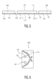
- Fig. 5 is a cross-sectional view (along a dotted line 452 shown in Fig. 4 ) of the single-sided contact base structure 450 depicted in Fig. 4 .
- the single-sided contact base structure 450 includes the contact layer 102 with the groove lines 124-1, 124-2, the adhesive layer 103 and the substrate 104.
- the bonding holes 426 are present on the substrate to enable future wire bonding.
- Fig. 6 depicts a portion 650 of one of the single-sided contact base structures 450 (at an area 454 shown in Fig. 4 ) of the single-sided contact tape with applied adhesive 610.
- glue or other adhesive material is applied (e.g., dispensed) to one of the single-sided contact base structure of the single-sided contact tape.
- the adhesive is applied to the single-sided contact tape in a shape that partially encircles bond holes 426.
- Fig. 7 is a cross-sectional view (along a dotted line 652 shown in Fig. 6 ) of the single-sided contact tape 440, which includes the single-sided contact tape portion 650 depicted in Fig. 6 .
- the single-sided contact tape includes the contact layer 102 with the groove lines 124-1, 124-2, the adhesive layer 103, the substrate 104, and the adhesive layer 106, which is formed from the applied adhesive 610.
- the manufacturing process proceeds to the next step in which antenna contact leads are attached to the single-sided contact tape using the applied adhesive to form a dual-interface contact tape with multiple dual-interface contact structures.
- the antenna contact leads can be attached to the single-sided contact tape by a pick-and-place process in which one or more antenna contact leads are picked up and placed on the single-sided contact tape.
- the antenna contact leads can be attached to the single-sided contact tape in a reel-to-reel process in which adhesive is applied to the antenna contact leads on a first reel, which is then applied onto a second reel, i.e., the single-sided contact tape, similar to the process of attaching a sheet of paper labels onto products.
- Fig. 8 depicts a portion 850 of the dual-interface contact tape with an attached antenna contact lead 808, which is part of a single dual-interface contact structure.
- the dual-interface contact tape portion 850 corresponds to the single-sided contact tape portion 650 of Fig. 6 .
- the antenna contact lead 808 is attached to the single-sided contact tape 440 via the applied adhesive 610 (shown in Figs. 6 and 7 ).
- the antenna contact lead can be attached to the single-sided contact tape by applying an adhesive to the antenna contact lead and then placing antenna contact lead with the adhesive on the single-sided contact tape.
- the antenna contact lead 808 depicted in Fig. 8 is one possible embodiment of the antenna contact leads 108 depicted in Fig. 1 .
- the antenna contact leads 108 depicted in Fig. 1 are not limited to the embodiment shown in Fig. 8 .
- Fig. 9 is a cross-sectional view (along a dotted line 852 shown in Fig. 6 ) of the dual-interface contact tape, which includes the dual-interface contact structure portion 850 depicted in Fig. 8 .
- Fig. 9 shows a single dual-interface contact structure formed within the dual-interface contact tape.
- the dual-interface contact structure includes the contact layer 102 with the groove lines 124-1, 124-2, the adhesive layer 103, the substrate 104, the adhesive layer 106, and two antenna contact leads 808.
- a curing step e.g., oven curing
- the dual-interface contact structure of Fig. 9 is made from an inexpensive single-sided contact tape, the cost of the dual-interface contact structure is significantly lower than a comparable conventional dual-interface contact structure made from an expensive double-sided contact tape.
- the antenna contact leads 808 shown in Figs. 8 and 9 are produced from a sheet of conductive material.
- Fig. 10 depicts a sheet of conductive material 1060 that includes four rows of antenna contact leads 808.
- each row includes two A-shaped antenna contact leads.
- Each A-shaped antenna contact lead has an approximate size of 6.8 millimeter (mm) x 3.7mm.
- Fig. 10 specific examples of dimension parameters of the A-shaped antenna contact leads are shown.
- dimension parameters of the antenna contact leads 108 depicted in Fig. 1 are not limited to the embodiment shown in Fig. 10 .
- the A-shaped antenna contact leads 808 are punched out of the sheet of conductive material.
- the A-shaped antenna contact leads are etched or laser cut out of the sheet of conductive material or additively deposited on a substrate by galvano plating or conductive printing.
- Fig. 11 depicts an embodiment of a dual-interface contact tape 1140 having multiple dual-interface IC chip modules 1150, which are formed by attaching the IC chips 110 to dual-interface contact structures, attaching the bond wires 112 to the antenna contact leads 808 and to the contact layer 102 (not shown in Fig.
- a separation (e.g., punching or cutting) step can then be performed to separate (e.g., punch out or cut) the dual-interface contact tape 1140 to separate the dual-interface IC chip modules 1150 into individual pieces.
- a punching process can be performed based on the outline shown in Fig. 4 to separate the dual-interface IC chip modules into individual pieces after a hotmelt tape is applied to the backside of the tape 440.
- the dual-interface IC chip module 1150 depicted in Fig. 11 is one possible embodiment of the dual-interface IC chip module 150 depicted in Fig. 1 .
- the dual-interface IC chip module 150 depicted in Fig. 1 is not limited to the embodiment shown in Fig. 11 .
- Fig. 12 is a cross-sectional view (along a dotted line 1152 shown in Fig. 11 ) of one of the dual-interface IC chip modules 1150 depicted in Fig. 11 .
- the dual-interface IC chip module includes the contact layer 102 with the groove lines 124-1, 124-2, the adhesive layer 103, the substrate 104, the adhesive layer 106, the two antenna contact leads 808, the IC chip 110, the bond wires 112, and the encapsulation 114.
- the adhesives 116 are used to attach the dual-interface IC chip module 150, which may be formed in the same manner as the dual-interface IC chip module 1150, to the card body 122.
- the adhesives may be made of a suitable material, such as film material or gel material (e.g., epoxy, acrylate).
- the adhesives are made of a hot melt adhesive material, such as adhesive epoxy or any other thermoplastic material, which becomes viscous with heat.
- the electrical connection layer 118 of the dual-interface IC card 100 is used to provide electrical connectivity between the antenna contact leads 108 and the antenna layer 120.
- the electrical connection layer may be made of any suitable conductive material.
- the electrical connection layer may be made of a conductive adhesive, a solder or a conductive polymeric material.
- the antenna layer 120 of the dual-interface IC card 100 is used to communicate wirelessly with another device (e.g., a card reader).
- the antenna layer may be made of metal or other suitable material.
- the antenna layer is made of a metal coil, such as a copper coil.
- the antenna layer may be of any suitable shape, including (without being limited to) circular, rectangular and square shapes.
- the card body 122 of the dual-interface IC card 100 is used to protect other components of the dual-interface IC card and well as to give shape to the dual-interface IC card.
- the card body may be made of plastic or other suitable material.
- an assembly step can be performed by attaching the antenna layer 120 and the card body to the dual-interface IC chip module 150 to produce the dual-interface IC card.
- Fig. 13 is a process flow diagram of a method for manufacturing a dual-interface IC card component in accordance with an embodiment of the invention.
- a single-sided contact base structure is obtained, where the single-sided contact base structure includes a substrate with an electrical contact layer.
- the single-sided contact base structure is part of a single-sided contact tape, such as the single-sided contact tape 440 shown in Figs. 4 and 5 .
- at least one antenna contact lead is attached to the single-sided contact base structure to form a dual-interface contact structure, which is a component of a dual-interface IC chip module of a dual-interface IC card.
- the dual-interface contact structure is part of a dual-interface contact tape, such as the dual-interface contact tape shown in Figs. 8 and 9 .
- Fig. 14 is a process flow diagram of a method for manufacturing a dual-interface IC card component in accordance with an embodiment of the invention.
- a single-sided contact tape that contains at least one column of single-sided base structure is obtained.
- the single-sided contact tape includes a substrate with an electrical contact layer.
- an adhesive material is applied to the substrate of the single-sided contact tape.
- antenna contact leads are obtained from a sheet of conductive material.
- the antenna contact leads are attached to the single-sided contact tape using the applied adhesive material to form dual-interface base structures.
Landscapes
- Engineering & Computer Science (AREA)
- Computer Hardware Design (AREA)
- Microelectronics & Electronic Packaging (AREA)
- Physics & Mathematics (AREA)
- General Physics & Mathematics (AREA)
- Theoretical Computer Science (AREA)
- Credit Cards Or The Like (AREA)
Abstract
Description
- Embodiments of the invention relate generally to electronic circuits and, more particularly, to integrated circuit (IC) devices and methods for manufacturing IC devices.
- An IC card, such as a smart card, includes an embedded integrated circuit that can be used to store information and perform data processing. For example, a portable IC card can be used in financial, transportation, security, healthcare, or other applications to provide identification and authentication. Types of IC cards include contact IC cards that communicate via electrical contacts, contactless IC cards that communicate wirelessly through antennas, and dual-interface IC cards that communicate via electrical contacts and wirelessly through antennas. Compared to contact IC cards and contactless IC cards, dual-interface IC cards allow users to switch between contact card readers and contactless card readers. However, since dual-interface IC cards include both electrical contacts and antennas, the dual-interface IC cards are more expensive to manufacture than contact IC cards and contactless IC cards. Therefore, there is a need for low-cost dual-interface IC card components and manufacturing dual-interface IC card components in a cost-effective manner.
- Dual-interface Integrated Circuit (IC) card components and methods for manufacturing the dual-interface IC card components are described. In an embodiment, a dual-interface IC card component includes a single-sided contact base structure, which includes a substrate with an electrical contact layer. On the single-sided contact base structure, one or more antenna contact leads are attached to the single-sided contact base structure to form a dual-interface contact structure, which is a component of a dual-interface IC card. The dual-interface contact structure is more cost-effective than using a prefabricated dual-interface contact tape currently available in the marketplace, which is typically made from scratch using etching or stamping technology. Other embodiments are also described.
- In an embodiment, a method for manufacturing a dual-interface IC card component involves obtaining a single-sided contact base structure, where the single-sided contact base structure includes a substrate with an electrical contact layer, and attaching at least one antenna contact lead to the single-sided contact base structure to form a dual-interface contact structure, which is a component of a dual-interface IC card.
- In an embodiment, a method for manufacturing a dual-interface IC card component involves obtaining a single-sided contact tape that contains at least one column of single-sided base structures, where the single-sided contact tape includes a substrate with an electrical contact layer, applying an adhesive material to the substrate of the single-sided contact tape, obtaining antenna contact leads from a sheet of conductive material, and attaching the antenna contact leads to the single-sided contact tape using the applied adhesive material to form dual-interface contact structures.
- In an embodiment, a dual-interface IC card component includes a substrate, an electrical contact layer attached to a first side of the substrate, and at least one antenna contact lead glued to a second, opposite, side of the substrate. The electrical contact layer includes a contact plate and multiple grooves.
- Other aspects and advantages of embodiments of the present invention will become apparent from the following detailed description, taken in conjunction with the accompanying drawings, depicted by way of example of the principles of the invention.
-
Fig. 1 is a cross-sectional view of a dual-interface IC card in accordance with an embodiment of the invention. -
Fig. 2 depicts a front-side view of an embodiment of a dual-interface IC chip module of the dual-interface IC card depicted inFig. 1 . -
Fig. 3 depicts a back-side view of the dual-interface IC chip module depicted inFig. 2 . -
Fig. 4 depicts an embodiment of a single-sided contact tape, which is used to produce a dual-interface contact base structure for the dual-interface IC chip module depicted inFig. 2 . -
Fig. 5 is a cross-sectional view of a single-sided contact tape depicted inFig. 4 . -
Fig. 6 depicts an embodiment of a single-sided contact tape with adhesive material applied to the tape. -
Fig. 7 is a cross-sectional view of the single-sided contact tape depicted inFig. 6 . -
Fig. 8 depicts an embodiment of a dual-interface contact structure having an antenna contact lead. -
Fig. 9 is a cross-sectional view of the dual-interface contact structure depicted inFig. 8 . -
Fig. 10 depicts an embodiment of a sheet of metal material with defined columns of antenna contact leads. -
Fig. 11 depicts an embodiment of a reel of dual-interface IC chip modules produced using the dual-interface contact structure depicted inFigs. 8 and 9 . -
Fig. 12 is a cross-sectional view of a single dual-interface IC chip module depicted inFig. 11 . -
Fig. 13 is a process flow diagram of a method for manufacturing a dual-interface IC card component in accordance with an embodiment of the invention. -
Fig. 14 is a process flow diagram of a method for manufacturing a dual-interface IC card component in accordance with another embodiment of the invention. - Throughout the description, similar reference numbers may be used to identify similar elements.
- It will be readily understood that the components of the embodiments as generally described herein and illustrated in the appended figures could be arranged and designed in a wide variety of different configurations. Thus, the following detailed description of various embodiments, as represented in the figures, is not intended to limit the scope of the present disclosure, but is merely representative of various embodiments. While the various aspects of the embodiments are presented in drawings, the drawings are not necessarily drawn to scale unless specifically indicated.
- The described embodiments are to be considered in all respects only as illustrative and not restrictive. The scope of the invention is, therefore, indicated by the appended claims rather than by this detailed description. All changes which come within the meaning and range of equivalency of the claims are to be embraced within their scope.
- Reference throughout this specification to features, advantages, or similar language does not imply that all of the features and advantages that may be realized with the present invention should be or are in any single embodiment. Rather, language referring to the features and advantages is understood to mean that a specific feature, advantage, or characteristic described in connection with an embodiment is included in at least one embodiment. Thus, discussions of the features and advantages, and similar language, throughout this specification may, but do not necessarily, refer to the same embodiment.
- Furthermore, the described features, advantages, and characteristics of the invention may be combined in any suitable manner in one or more embodiments. One skilled in the relevant art will recognize, in light of the description herein, that the invention can be practiced without one or more of the specific features or advantages of a particular embodiment. In other instances, additional features and advantages may be recognized in certain embodiments that may not be present in all embodiments of the invention.
- Reference throughout this specification to "one embodiment," "an embodiment," or similar language means that a particular feature, structure, or characteristic described in connection with the indicated embodiment is included in at least one embodiment. Thus, the phrases "in one embodiment," "in an embodiment," and similar language throughout this specification may, but do not necessarily, all refer to the same embodiment.
-
Fig. 1 is a cross-sectional view of a dual-interface IC card 100 in accordance with an embodiment of the invention. The dual-interface IC card can be used in financial, transportation, security, healthcare, or other applications to store information and perform data processing. In some embodiments, the dual-interface IC card has the ability to securely manage, store and provide access to data on the card, perform on-card functions, such as encryption, authentication, and authorization, and interact intelligently with a card reader. The dual-interface IC card can communicate by electrical contacts or wirelessly through an antenna. In an embodiment, the dual-interface IC card is a smart card, which can be used in Near field communication (NFC) applications. In some embodiments, the IC card is a smart card that is designed to be compatible with the International Organization for Standardization (ISO)/ the International Electrotechnical Commission (IEC) 14443. As described in more detail below, the manufacturing cost of the dual-interface IC card can be significantly lower than conventional dual-interface IC cards because the dual-interface IC card can be produced using a prefabricated single-sided contact base structure that is used to make a module for a contact smart card (e.g., a standard single-sided contact tape currently available in the marketplace), rather than a more expensive prefabricated double-sided contact base structure that is used to make a module for a dual-interface smart card (e.g., a standard double-sided contact tape currently available in the market). - In the embodiment depicted in
Fig. 1 , the dual-interface IC card 100 includes acontact layer 102, asubstrate 104, anadhesive layer 106, antenna contact leads 108, anIC chip 110,bond wires 112, anencapsulation 114,adhesives 116, anelectrical connection layer 118, anantenna layer 120, and acard body 122. Although the dual-interface IC card is shown inFig. 1 as including certain components, in other embodiments, the dual-interface IC card may include fewer components or additional components that are commonly found in conventional dual-interface smart cards. - The
contact layer 102 of the dual-interface IC card 100 is used to make electrical contacts with a card reader to communicate with the card reader. In some embodiments, the contact layer is located at the front side of the dual-interface IC card while thecard body 122 is located at the back side of the dual-interface IC card. The contact layer may be made of metal or other conductive material. In some embodiments, the contact layer is made of Gold (Au)-Nickel (Ni) plated Copper (Cu) foil or galvano deposited Cu. The contact layer, which is also referred to as the contact pad, provides electrical connectivity when the dual-interface IC card is inserted into a card reader. In some embodiments, the contact layer is designed and produced to be compatible with the International Organization for Standardization (ISO) 7816. The contact layer typically includes groove/recess lines used to electrically insulate contact areas of the contact layer from each other and make the contact layer more flexible. In the embodiment depicted inFig. 1 , the contact layer has two groove lines 124-1, 124-2. However, in other embodiments, the contact layer may have any number of groove lines. - The
substrate 104 is used to support other elements of the dual-interface IC card 100, such as thecontact layer 102, the antenna contact leads 108 and theIC chip 110. The substrate may be made of any suitable substrate material. As an example, the substrate may be made of Epoxy glass, fiberglass, or plastic substrates (Polyethylene naphthalate (PEN), etc.). In the embodiment depicted inFig. 1 , bonding holes 126 are present on the substrate to enable wire bonding of theIC chip 100 to the contact layer, which are located on opposite sides of the substrate. The substrate may be in the form of a sheet or a tape. In some embodiments, the contact layer and the substrate form a single-sided contact base structure, which may be packaged into a single-sided contact tape. For example, a device manufacturer may produce a prefabricated single-sided contact base structure that includes the contact layer and the substrate in mass quantities. In some embodiments, an optionaladhesive layer 103 is located between the contact layer and the substrate. - The
adhesive layer 106 of the dual-interface IC card 100 is used to attach the antenna contact leads 108 onto thesubstrate 104. Theadhesive layer 106 may be made of any suitable adhesive material. In some embodiments, theadhesive layer 106 is made of glue. The adhesive layer can be formed by applying an adhesive material (e.g., glue) on the substrate and/or the antenna contact leads by various processes. For example, the adhesive material may be dispense on the substrate or pre-applied on the antenna contact leads. A curing process (e.g., oven curing) may then be performed to cure the adhesive material. - The antenna contact leads 108 of the dual-
interface IC card 100 are used to provide electrical contacts between an antenna (e.g., the antenna layer 120) and theIC chip 110. The antenna contact leads may be made of any suitable conductive material. For example, the antenna contact leads may be made of a metal foil or a metal laminate, which includes a metal foil and a substrate. In some embodiments, the antenna contact leads are made of gold and nickel (Au-Ni) plated copper (Cu) or silver (Ag) plated stainless steel. The antenna contact leads may be made in any suitable dimensions. In some embodiments, the antenna contact leads have a uniform thickness. For example, the thickness of the antenna contact leads may be in the range of between 10 micrometers (µm) and 100µm, which overlaps with the standard thickness for antenna contact leads (e.g., between 18 µm and 35µm for Cu foil) of smart cards. The antenna contact leads can be produced by any suitable process, including (without being limited to), punching, etching and laser cutting a sheet of conductive material. In some embodiments, the antenna contact leads are produced by punching either a standalone conductive sheet or a conductive sheet in a reel-to-reel format. In some embodiments, the antenna contact leads are produced by depositing a metal layer on a plastic substrate material. In some embodiments, the antenna contact leads are plated with suitable material, such as Ni, Au and/or Ag, for better antenna attachment or for better wire bond attachment. The antenna contact leads may be made of any suitable shape or dimension. In some embodiments, the antenna contact leads are designed and produced with features to ease the interconnection process with thesubstrate 104. For example, one or more antenna contact leads may have a spring like feature or may be crimped to improve adhesion of the conductive material (e.g., glue etc.) used in the interconnection process. The antenna contact leads can be attached to thesubstrate 104 by a pick-and-place process in which one or more antenna contact leads are picked up and placed on the substrate. Alternatively, the antenna contact leads can be attached to the substrate in a reel-to-reel process in which adhesive is applied to the antenna contact leads on a first reel, which is then applied onto a second reel, i.e., the single-sided contact tape, similar to the process of attaching a sheet of paper labels onto products. In some embodiments, instead of contact leads, a primary antenna structure is applied to thesubstrate 104 by a pick-and-place process in which the primary antenna structure is picked up and placed on the substrate. Although the antenna contact leads are shown inFig. 1 as being electrically connected to theantenna layer 120 through theelectrical connection layer 118, in other embodiments, the antenna contact leads may be in direct contact with the antenna layer. In addition, in other embodiments, the antenna contact leads are either connected to an antenna located on thesubstrate 104 or connected to a small antenna directly placed on the substrate, to be compliant with ISO/IEC 14443 requirements. In these embodiments, theantenna layer 120 acts as a "booster" antenna, which is electromagnetically coupled to the antenna located on the substrate. - In some embodiments, the
contact layer 102, thesubstrate 104, theadhesive layer 106, and the antenna contact leads 108 form a dual-interface contact structure, which may be produced in mass quantities. For example, a device manufacturer can produce dual-interface contact structures in mass quantities based on prefabricated single-sided contact base structures, such as prefabricated single-sided contact tapes provided by Linxens, Interplex, Kinsus, LG Innotek and Possehl. - The
IC chip 110 of the dual-interface IC card 100 includes circuitry to securely manage, store and provide access to data on the card and/or perform on-card functions, such as encryption, authentication, and authorization. The IC chip is designed to communicate with another device (e.g., a card reader) by electrical contacts or wirelessly through an antenna. In the embodiment depicted inFig. 1 , the dual-interface IC card includes a single IC chip with both contact and contactless interfaces, which makes is possible to access theIC chip 110 using either a contact interface (e.g., the contact layer 102) or a contactless interface (e.g., the antenna layer 120) with a high level of security. Alternatively, the dual-interface IC card may include two IC chips, including one IC chip with a contact interface and another, separated, IC chip with a contactless interface. The IC chip may be attached to thesubstrate 104 using any appropriate method. As an example, in some embodiments, the IC chip is glued onto the substrate using anadhesive layer 107. - The bond wires 112-1, 112-2 of the dual-
interface IC card 100 are used to electrically connect theIC chip 110 to thecontact layer 102 and to theantenna layer 120. The bond wires may be made of any suitable metal (e.g., aluminum or copper). In the embodiment depicted inFig. 1 , the bond wire 112-1 electrically connects the IC chip to the antenna contact leads 108, which is electrically connected to theantenna layer 120, while the bond wire 112-2 electrically connects the IC chip to the contact layer. Bond pads may be used to attach the bond wires to the IC chip, the antenna contact leads, and/or the contact layer. In other embodiments, the connections between the bond wires and the contact layer or antenna contact leads may be different from the connections shown inFig. 1 . - The
encapsulation 114 of the dual-interface IC card 100 is used to protect thebond wires 112 and theIC chip 110. The encapsulation may be made of a suitable material, such as epoxy, in a process such as glob-top or molding - In some embodiments, the
contact layer 102, thesubstrate 104, theadhesive layer 106, the antenna contact leads 108, theIC chip 110, thebond wires 112, and theencapsulation 114 form a dual-interfaceIC chip module 150. A device manufacturer may produce dual-interface IC chip modules in mass quantities. For example, a device manufacturer may produce dual-interface IC chip modules in mass quantities based on dual-interface contact structures. Each dual-interface contact structure includes the contact layer, the substrate, the adhesive layer, and the antenna contact leads. -
Fig. 2 depicts a front-side view of an embodiment of the dual-interfaceIC chip module 150 depicted inFig. 1 . In the embodiment depicted inFig. 2 , a front-side view of a dual-interfaceIC chip module 250 shows acontact layer 202, which includes acontact plate 232 andgroove lines 224. Thecontact layer 202 depicted inFig. 2 is one possible embodiment of thecontact layer 102 depicted inFig. 1 . However, thecontact layer 102 depicted inFig. 1 is not limited to the embodiment shown inFig. 2 . For example, thecontact layer 102 depicted inFig. 1 may have groove/recess lines that are different from thegroove lines 224 shown inFig. 2 . -
Fig. 3 depicts a back-side view of the dual-interfaceIC chip module 250 depicted inFig. 2 . In the embodiment depicted inFig. 3 , a back-side view of the dual-interface IC chip module shows anIC chip 310,bond wires 312, and A-shaped antenna contact leads 308. The embodiment of the antenna contact leads 308 depicted inFig. 3 is a possible embodiment of the antenna contact leads 108 depicted inFig. 1 . However, the antenna contact leads 108 depicted inFig. 1 are not limited to the embodiment shown inFig. 3 . For example, the antenna contact leads 108 depicted inFig. 1 can be implemented in a shape that is different from the antenna contact leads shown inFig. 3 . - A process of manufacturing the dual-interface
IC chip module 150 depicted inFig. 1 in accordance with an embodiment of the invention is described with reference toFigs. 4-12 . Compared with a conventional manufacturing process in which a dual-interface IC chip module is made using a relatively expensive double-sided contact tape as a base structure, the manufacturing process produces the dual-interfaceIC chip module 150 using a cost-effective prefabricated single-sided contact base structure, e.g., a single-sided contact tape, and antenna contact leads that are attached to the single-sided contact base structure. By using the prefabricated single-sided contact base structure, the cost of the dual-interface IC chip module is significantly reduced. - As illustrated in
Fig. 4 , the process of manufacturing the dual-interfaceIC chip module 150 begins by obtaining a single-sided contact tape 440 having multiple single-sidedcontact base structures 450. InFig. 4 , the single-sided contact tape 440 includes two columns of single-sidedcontact base structures 450. As shown inFig. 4 , a back-side view of the single-sided contact tape shows the back-side of single-sided contact base structures with bonding holes 426. The single-sided contact tape may be in the form of standalone sheet or in a reel-to-reel format. Although the single-sided contact tape is shown inFig. 4 as including two columns of single-sided contact base structures, in other embodiment, the single-sided contact tape may include a single column or more than two column of single-sided contact base structures. In addition, although the single-sidedcontact base structure 450 is shown inFig. 4 as including certain number of bonding holes, in other embodiment, the single-sided contact base structure may include bond holes in any suitable number. The single-sided contact tape may be obtained by purchasing it from a tape supplier, such as Linxens, Interplex, Kinsus, LG Innotek and Possehl. Alternatively, the single-sided contact tape may be obtained by making it from scratch using a known manufacturing process. -
Fig. 5 is a cross-sectional view (along a dottedline 452 shown inFig. 4 ) of the single-sidedcontact base structure 450 depicted inFig. 4 . In the embodiment ofFig. 5 , the single-sidedcontact base structure 450 includes thecontact layer 102 with the groove lines 124-1, 124-2, theadhesive layer 103 and thesubstrate 104. The bonding holes 426 are present on the substrate to enable future wire bonding. - After obtaining the single-
sided contact tape 440, the manufacturing process proceeds to the next step in which adhesive is applied to the single-sided contact tape.Fig. 6 depicts aportion 650 of one of the single-sided contact base structures 450 (at anarea 454 shown inFig. 4 ) of the single-sided contact tape with applied adhesive 610. InFig. 6 , glue or other adhesive material is applied (e.g., dispensed) to one of the single-sided contact base structure of the single-sided contact tape. As shown inFig. 6 , the adhesive is applied to the single-sided contact tape in a shape that partially encircles bond holes 426. -
Fig. 7 is a cross-sectional view (along a dottedline 652 shown inFig. 6 ) of the single-sided contact tape 440, which includes the single-sidedcontact tape portion 650 depicted inFig. 6 . InFig. 7 , the single-sided contact tape includes thecontact layer 102 with the groove lines 124-1, 124-2, theadhesive layer 103, thesubstrate 104, and theadhesive layer 106, which is formed from the appliedadhesive 610. - After the adhesive 610 has been applied to the single-
sided contact tape 440, the manufacturing process proceeds to the next step in which antenna contact leads are attached to the single-sided contact tape using the applied adhesive to form a dual-interface contact tape with multiple dual-interface contact structures. The antenna contact leads can be attached to the single-sided contact tape by a pick-and-place process in which one or more antenna contact leads are picked up and placed on the single-sided contact tape. Alternatively, the antenna contact leads can be attached to the single-sided contact tape in a reel-to-reel process in which adhesive is applied to the antenna contact leads on a first reel, which is then applied onto a second reel, i.e., the single-sided contact tape, similar to the process of attaching a sheet of paper labels onto products.Fig. 8 depicts aportion 850 of the dual-interface contact tape with an attachedantenna contact lead 808, which is part of a single dual-interface contact structure. The dual-interfacecontact tape portion 850 corresponds to the single-sidedcontact tape portion 650 ofFig. 6 . InFig. 8 , theantenna contact lead 808 is attached to the single-sided contact tape 440 via the applied adhesive 610 (shown inFigs. 6 and7 ). Alternatively, the antenna contact lead can be attached to the single-sided contact tape by applying an adhesive to the antenna contact lead and then placing antenna contact lead with the adhesive on the single-sided contact tape. Theantenna contact lead 808 depicted inFig. 8 is one possible embodiment of the antenna contact leads 108 depicted inFig. 1 . However, the antenna contact leads 108 depicted inFig. 1 are not limited to the embodiment shown inFig. 8 . -
Fig. 9 is a cross-sectional view (along a dottedline 852 shown inFig. 6 ) of the dual-interface contact tape, which includes the dual-interfacecontact structure portion 850 depicted inFig. 8 . In particular,Fig. 9 shows a single dual-interface contact structure formed within the dual-interface contact tape. As shown inFig. 9 , the dual-interface contact structure includes thecontact layer 102 with the groove lines 124-1, 124-2, theadhesive layer 103, thesubstrate 104, theadhesive layer 106, and two antenna contact leads 808. A curing step (e.g., oven curing) may be performed by applying heat to the dual-interface contact structure. Since the dual-interface contact structure ofFig. 9 is made from an inexpensive single-sided contact tape, the cost of the dual-interface contact structure is significantly lower than a comparable conventional dual-interface contact structure made from an expensive double-sided contact tape. - In an embodiment, the antenna contact leads 808 shown in
Figs. 8 and 9 are produced from a sheet of conductive material. As an example,Fig. 10 depicts a sheet of conductive material 1060 that includes four rows of antenna contact leads 808. In the illustrated embodiment, each row includes two A-shaped antenna contact leads. Each A-shaped antenna contact lead has an approximate size of 6.8 millimeter (mm) x 3.7mm. InFig. 10 , specific examples of dimension parameters of the A-shaped antenna contact leads are shown. However, dimension parameters of the antenna contact leads 108 depicted inFig. 1 are not limited to the embodiment shown inFig. 10 . In the embodiment depicted inFig. 10 , the A-shaped antenna contact leads 808 are punched out of the sheet of conductive material. However, in other embodiments, the A-shaped antenna contact leads are etched or laser cut out of the sheet of conductive material or additively deposited on a substrate by galvano plating or conductive printing. - After the antenna contact leads 808 have been attached to the single-
sided contact tape 440 to form the dual-interface contact tape, the manufacturing process proceeds to the next step in which IC chips, bond wires and encapsulations are added to the dual-interface contact structures in the dual-interface contact tape to form dual-interface IC chip modules in the dual-interface contact tape.Fig. 11 depicts an embodiment of a dual-interface contact tape 1140 having multiple dual-interfaceIC chip modules 1150, which are formed by attaching the IC chips 110 to dual-interface contact structures, attaching thebond wires 112 to the antenna contact leads 808 and to the contact layer 102 (not shown inFig. 11 ), and then forming theencapsulations 114 over the IC chips and the bond wires. A separation (e.g., punching or cutting) step can then be performed to separate (e.g., punch out or cut) the dual-interface contact tape 1140 to separate the dual-interfaceIC chip modules 1150 into individual pieces. For example, a punching process can be performed based on the outline shown inFig. 4 to separate the dual-interface IC chip modules into individual pieces after a hotmelt tape is applied to the backside of thetape 440. The dual-interfaceIC chip module 1150 depicted inFig. 11 is one possible embodiment of the dual-interfaceIC chip module 150 depicted inFig. 1 . However, the dual-interfaceIC chip module 150 depicted inFig. 1 is not limited to the embodiment shown inFig. 11 . -
Fig. 12 is a cross-sectional view (along a dottedline 1152 shown inFig. 11 ) of one of the dual-interfaceIC chip modules 1150 depicted inFig. 11 . As shown inFig. 12 , the dual-interface IC chip module includes thecontact layer 102 with the groove lines 124-1, 124-2, theadhesive layer 103, thesubstrate 104, theadhesive layer 106, the two antenna contact leads 808, theIC chip 110, thebond wires 112, and theencapsulation 114. - Turning back to
Fig. 1 , theadhesives 116 are used to attach the dual-interfaceIC chip module 150, which may be formed in the same manner as the dual-interfaceIC chip module 1150, to thecard body 122. The adhesives may be made of a suitable material, such as film material or gel material (e.g., epoxy, acrylate). In an embodiment, the adhesives are made of a hot melt adhesive material, such as adhesive epoxy or any other thermoplastic material, which becomes viscous with heat. - The
electrical connection layer 118 of the dual-interface IC card 100 is used to provide electrical connectivity between the antenna contact leads 108 and theantenna layer 120. The electrical connection layer may be made of any suitable conductive material. For example, the electrical connection layer may be made of a conductive adhesive, a solder or a conductive polymeric material. - The
antenna layer 120 of the dual-interface IC card 100 is used to communicate wirelessly with another device (e.g., a card reader). The antenna layer may be made of metal or other suitable material. In some embodiments, the antenna layer is made of a metal coil, such as a copper coil. The antenna layer may be of any suitable shape, including (without being limited to) circular, rectangular and square shapes. - The
card body 122 of the dual-interface IC card 100 is used to protect other components of the dual-interface IC card and well as to give shape to the dual-interface IC card. The card body may be made of plastic or other suitable material. In some embodiments, an assembly step can be performed by attaching theantenna layer 120 and the card body to the dual-interfaceIC chip module 150 to produce the dual-interface IC card. -
Fig. 13 is a process flow diagram of a method for manufacturing a dual-interface IC card component in accordance with an embodiment of the invention. Atblock 1302, a single-sided contact base structure is obtained, where the single-sided contact base structure includes a substrate with an electrical contact layer. In some embodiments, the single-sided contact base structure is part of a single-sided contact tape, such as the single-sided contact tape 440 shown inFigs. 4 and5 . Atblock 1304, at least one antenna contact lead is attached to the single-sided contact base structure to form a dual-interface contact structure, which is a component of a dual-interface IC chip module of a dual-interface IC card. In some embodiments, the dual-interface contact structure is part of a dual-interface contact tape, such as the dual-interface contact tape shown inFigs. 8 and 9 . -
Fig. 14 is a process flow diagram of a method for manufacturing a dual-interface IC card component in accordance with an embodiment of the invention. Atblock 1402, a single-sided contact tape that contains at least one column of single-sided base structure is obtained. The single-sided contact tape includes a substrate with an electrical contact layer. Atblock 1404, an adhesive material is applied to the substrate of the single-sided contact tape. Atblock 1406, antenna contact leads are obtained from a sheet of conductive material. Atblock 1408, the antenna contact leads are attached to the single-sided contact tape using the applied adhesive material to form dual-interface base structures. - Although the operations of the method herein are shown and described in a particular order, the order of the operations of the method may be altered so that certain operations may be performed in an inverse order or so that certain operations may be performed, at least in part, concurrently with other operations. In another embodiment, instructions or sub-operations of distinct operations may be implemented in an intermittent and/or alternating manner.
- In addition, although specific embodiments of the invention that have been described or depicted include several components described or depicted herein, other embodiments of the invention may include fewer or more components to implement less or more feature.
- Furthermore, although specific embodiments of the invention have been described and depicted, the invention is not to be limited to the specific forms or arrangements of parts so described and depicted. The scope of the invention is to be defined by the claims appended hereto and their equivalents.
Claims (15)
- A method for manufacturing a dual-interface integrated circuit (IC) card component, the method comprising:obtaining a single-sided contact base structure, wherein the single-sided contact base structure comprises a substrate with an electrical contact layer; andattaching at least one antenna contact lead to the single-sided contact base structure to form a dual-interface contact structure, which is a component of a dual-interface IC card.
- The method of claim 1, wherein attaching the at least one antenna contact lead to the single-sided contact base structure comprises:picking up an antenna contact lead; andplacing the antenna contact lead on the single-sided contact base structure to attach the antenna contact lead to the single-sided contact base structure.
- The method of claim 1 or 2, wherein attaching the at least one antenna contact lead to the single-sided contact base structure comprises:applying an adhesive material to the substrate of the single-sided contact base structure; andplacing an antenna contact lead on the applied adhesive material to attach the antenna contact lead to the single-sided contact base structure.
- The method of claim 3, wherein applying the adhesive material to the substrate comprises dispensing glue onto the substrate.
- The method of claim 3 or 4, further comprising curing the adhesive material.
- The method of any preceding claim, wherein attaching the at least one antenna contact lead to the single-sided contact base structure comprises:applying an adhesive material to an antenna contact lead; andplacing the antenna contact lead with the applied adhesive material on the single-sided contact base structure to attach the antenna contact lead to the single-sided contact base structure.
- The method of any preceding claim, wherein the contact layer is attached to a first side of the substrate, and wherein the at least one antenna contact lead is attached to a second, opposite, side of the substrate.
- The method of any preceding claim, further comprising obtaining the at least one antenna contact lead by punching, etching or laser cutting a sheet of conductive material.
- The method of any preceding claim, wherein the at least one antenna contact lead is applied to the single-sided contact base structure in a reel-to-reel process.
- The method of any preceding claim, wherein the at least one antenna contact lead is crimped or has a spring like feature.
- The method of any preceding claim, wherein obtaining the single-sided contact base structure comprises obtaining a single-sided contact tape.
- The method of any preceding claim, wherein the at least one antenna contact lead is electrically connected to an antenna located on the substrate.
- The method of any preceding claim, further comprising attaching an IC chip, bond wires and an encapsulation to the dual-interface contact structure to produce a dual-interface IC chip module.
- A dual-interface integrated circuit (IC) card component, the dual-interface IC card component comprising:a substrate;an electrical contact layer attached to a first side of the substrate, the electrical contact layer comprising a contact plate and a plurality of grooves; andat least one antenna contact lead glued to a second, opposite, side of the substrate.
- The dual-interface IC card component of claim 14, further comprising:an IC chip attached to the substrate;bond wires electrically connected to the IC chip, the electrical contact layer and the at least one antenna contact lead; andan encapsulation over the IC chip.
Priority Applications (1)
| Application Number | Priority Date | Filing Date | Title |
|---|---|---|---|
| EP15162803.9A EP3079105B1 (en) | 2015-04-08 | 2015-04-08 | Dual-interface ic card components and method for manufacturing the dual-interface ic card components |
Applications Claiming Priority (1)
| Application Number | Priority Date | Filing Date | Title |
|---|---|---|---|
| EP15162803.9A EP3079105B1 (en) | 2015-04-08 | 2015-04-08 | Dual-interface ic card components and method for manufacturing the dual-interface ic card components |
Publications (2)
| Publication Number | Publication Date |
|---|---|
| EP3079105A1 true EP3079105A1 (en) | 2016-10-12 |
| EP3079105B1 EP3079105B1 (en) | 2021-03-31 |
Family
ID=52823509
Family Applications (1)
| Application Number | Title | Priority Date | Filing Date |
|---|---|---|---|
| EP15162803.9A Active EP3079105B1 (en) | 2015-04-08 | 2015-04-08 | Dual-interface ic card components and method for manufacturing the dual-interface ic card components |
Country Status (1)
| Country | Link |
|---|---|
| EP (1) | EP3079105B1 (en) |
Citations (3)
| Publication number | Priority date | Publication date | Assignee | Title |
|---|---|---|---|---|
| US20070144662A1 (en) * | 2005-12-22 | 2007-06-28 | Armijo Edward A | Method of manufacturing RFID devices |
| US20080283615A1 (en) * | 2007-05-17 | 2008-11-20 | Advanced Microelectronic And Automation Technology Ltd. | Dual interface inlays |
| US20120193436A1 (en) * | 2011-01-31 | 2012-08-02 | American Bank Note Company | Dual-interface smart card |
Family Cites Families (1)
| Publication number | Priority date | Publication date | Assignee | Title |
|---|---|---|---|---|
| DE102007022615A1 (en) * | 2007-05-15 | 2008-11-20 | Infineon Technologies Ag | Contactless transmission system and method of making the same |
-
2015
- 2015-04-08 EP EP15162803.9A patent/EP3079105B1/en active Active
Patent Citations (3)
| Publication number | Priority date | Publication date | Assignee | Title |
|---|---|---|---|---|
| US20070144662A1 (en) * | 2005-12-22 | 2007-06-28 | Armijo Edward A | Method of manufacturing RFID devices |
| US20080283615A1 (en) * | 2007-05-17 | 2008-11-20 | Advanced Microelectronic And Automation Technology Ltd. | Dual interface inlays |
| US20120193436A1 (en) * | 2011-01-31 | 2012-08-02 | American Bank Note Company | Dual-interface smart card |
Also Published As
| Publication number | Publication date |
|---|---|
| EP3079105B1 (en) | 2021-03-31 |
Similar Documents
| Publication | Publication Date | Title |
|---|---|---|
| US11222861B2 (en) | Dual-interface IC card module | |
| US5598032A (en) | Hybrid chip card capable of both contact and contact-free operation and having antenna contacts situated in a cavity for an electronic module | |
| US5671525A (en) | Method of manufacturing a hybrid chip card | |
| US9536188B2 (en) | Dual-interface IC card components and method for manufacturing the dual-interface IC card components | |
| US20110011939A1 (en) | Contact-less and dual interface inlays and methods for producing the same | |
| US9390365B2 (en) | Integrated circuit module for a dual-interface smart card | |
| EP3384434B1 (en) | Method for embedding integrated circuit flip chip | |
| US10366320B2 (en) | Dual-interface IC card | |
| KR102190847B1 (en) | Method for manufacturing a flexible printed circuit, flexible printed circuit obtained by said method, and chip card module comprising such a flexible printed circuit | |
| CN103839098B (en) | Radio frequency identification for printing(RFID)The apparatus and method of label | |
| FI119401B (en) | Smart label web and process for its manufacture | |
| US11893821B2 (en) | Sensor device, method for forming a sensor device, carrier tape, chip card and method for forming a chip card | |
| US9424507B2 (en) | Dual interface IC card components and method for manufacturing the dual-interface IC card components | |
| US20080129455A1 (en) | Method for forming rfid tags | |
| US10706346B2 (en) | Method for manufacturing a smart card module and a smart card | |
| CN107111779B (en) | Method for manufacturing a single-sided electronic module comprising an interconnection zone | |
| US20060261456A1 (en) | Micromodule, particularly for chip card | |
| KR20060017779A (en) | Method for mounting an electronic component on a substrante | |
| EP3079105B1 (en) | Dual-interface ic card components and method for manufacturing the dual-interface ic card components | |
| US20170178991A1 (en) | Method for producing electronic devices | |
| CN115769225A (en) | Method of forming a pre-laminated inlay body for a smart card, method of forming a smart card, pre-laminated inlay body, and smart card | |
| JP2007114991A (en) | Composite ic card and ic module for composite ic card | |
| JP2008269648A (en) | Ic card common to contact type and noncontact type | |
| KR20030051442A (en) | Smart card having loop coil contact laminated metal plate and method for manufacturing the same | |
| JP2013033354A (en) | Antenna sheet for rfid, inlet for rfid, noncontact ic card and noncontact ic tag |
Legal Events
| Date | Code | Title | Description |
|---|---|---|---|
| PUAI | Public reference made under article 153(3) epc to a published international application that has entered the european phase |
Free format text: ORIGINAL CODE: 0009012 |
|
| AK | Designated contracting states |
Kind code of ref document: A1 Designated state(s): AL AT BE BG CH CY CZ DE DK EE ES FI FR GB GR HR HU IE IS IT LI LT LU LV MC MK MT NL NO PL PT RO RS SE SI SK SM TR |
|
| AX | Request for extension of the european patent |
Extension state: BA ME |
|
| STAA | Information on the status of an ep patent application or granted ep patent |
Free format text: STATUS: REQUEST FOR EXAMINATION WAS MADE |
|
| 17P | Request for examination filed |
Effective date: 20170412 |
|
| RBV | Designated contracting states (corrected) |
Designated state(s): AL AT BE BG CH CY CZ DE DK EE ES FI FR GB GR HR HU IE IS IT LI LT LU LV MC MK MT NL NO PL PT RO RS SE SI SK SM TR |
|
| STAA | Information on the status of an ep patent application or granted ep patent |
Free format text: STATUS: EXAMINATION IS IN PROGRESS |
|
| 17Q | First examination report despatched |
Effective date: 20180702 |
|
| STAA | Information on the status of an ep patent application or granted ep patent |
Free format text: STATUS: EXAMINATION IS IN PROGRESS |
|
| GRAP | Despatch of communication of intention to grant a patent |
Free format text: ORIGINAL CODE: EPIDOSNIGR1 |
|
| STAA | Information on the status of an ep patent application or granted ep patent |
Free format text: STATUS: GRANT OF PATENT IS INTENDED |
|
| INTG | Intention to grant announced |
Effective date: 20201113 |
|
| GRAJ | Information related to disapproval of communication of intention to grant by the applicant or resumption of examination proceedings by the epo deleted |
Free format text: ORIGINAL CODE: EPIDOSDIGR1 |
|
| STAA | Information on the status of an ep patent application or granted ep patent |
Free format text: STATUS: EXAMINATION IS IN PROGRESS |
|
| GRAP | Despatch of communication of intention to grant a patent |
Free format text: ORIGINAL CODE: EPIDOSNIGR1 |
|
| STAA | Information on the status of an ep patent application or granted ep patent |
Free format text: STATUS: GRANT OF PATENT IS INTENDED |
|
| GRAS | Grant fee paid |
Free format text: ORIGINAL CODE: EPIDOSNIGR3 |
|
| INTC | Intention to grant announced (deleted) | ||
| GRAA | (expected) grant |
Free format text: ORIGINAL CODE: 0009210 |
|
| STAA | Information on the status of an ep patent application or granted ep patent |
Free format text: STATUS: THE PATENT HAS BEEN GRANTED |
|
| INTG | Intention to grant announced |
Effective date: 20210203 |
|
| AK | Designated contracting states |
Kind code of ref document: B1 Designated state(s): AL AT BE BG CH CY CZ DE DK EE ES FI FR GB GR HR HU IE IS IT LI LT LU LV MC MK MT NL NO PL PT RO RS SE SI SK SM TR |
|
| REG | Reference to a national code |
Ref country code: GB Ref legal event code: FG4D Ref country code: CH Ref legal event code: EP |
|
| REG | Reference to a national code |
Ref country code: DE Ref legal event code: R096 Ref document number: 602015067383 Country of ref document: DE Ref country code: AT Ref legal event code: REF Ref document number: 1377779 Country of ref document: AT Kind code of ref document: T Effective date: 20210415 |
|
| REG | Reference to a national code |
Ref country code: IE Ref legal event code: FG4D |
|
| REG | Reference to a national code |
Ref country code: LT Ref legal event code: MG9D |
|
| PG25 | Lapsed in a contracting state [announced via postgrant information from national office to epo] |
Ref country code: BG Free format text: LAPSE BECAUSE OF FAILURE TO SUBMIT A TRANSLATION OF THE DESCRIPTION OR TO PAY THE FEE WITHIN THE PRESCRIBED TIME-LIMIT Effective date: 20210630 Ref country code: NO Free format text: LAPSE BECAUSE OF FAILURE TO SUBMIT A TRANSLATION OF THE DESCRIPTION OR TO PAY THE FEE WITHIN THE PRESCRIBED TIME-LIMIT Effective date: 20210630 Ref country code: FI Free format text: LAPSE BECAUSE OF FAILURE TO SUBMIT A TRANSLATION OF THE DESCRIPTION OR TO PAY THE FEE WITHIN THE PRESCRIBED TIME-LIMIT Effective date: 20210331 Ref country code: HR Free format text: LAPSE BECAUSE OF FAILURE TO SUBMIT A TRANSLATION OF THE DESCRIPTION OR TO PAY THE FEE WITHIN THE PRESCRIBED TIME-LIMIT Effective date: 20210331 |
|
| PG25 | Lapsed in a contracting state [announced via postgrant information from national office to epo] |
Ref country code: RS Free format text: LAPSE BECAUSE OF FAILURE TO SUBMIT A TRANSLATION OF THE DESCRIPTION OR TO PAY THE FEE WITHIN THE PRESCRIBED TIME-LIMIT Effective date: 20210331 Ref country code: LV Free format text: LAPSE BECAUSE OF FAILURE TO SUBMIT A TRANSLATION OF THE DESCRIPTION OR TO PAY THE FEE WITHIN THE PRESCRIBED TIME-LIMIT Effective date: 20210331 Ref country code: SE Free format text: LAPSE BECAUSE OF FAILURE TO SUBMIT A TRANSLATION OF THE DESCRIPTION OR TO PAY THE FEE WITHIN THE PRESCRIBED TIME-LIMIT Effective date: 20210331 |
|
| REG | Reference to a national code |
Ref country code: NL Ref legal event code: MP Effective date: 20210331 |
|
| REG | Reference to a national code |
Ref country code: AT Ref legal event code: MK05 Ref document number: 1377779 Country of ref document: AT Kind code of ref document: T Effective date: 20210331 |
|
| PG25 | Lapsed in a contracting state [announced via postgrant information from national office to epo] |
Ref country code: CZ Free format text: LAPSE BECAUSE OF FAILURE TO SUBMIT A TRANSLATION OF THE DESCRIPTION OR TO PAY THE FEE WITHIN THE PRESCRIBED TIME-LIMIT Effective date: 20210331 Ref country code: EE Free format text: LAPSE BECAUSE OF FAILURE TO SUBMIT A TRANSLATION OF THE DESCRIPTION OR TO PAY THE FEE WITHIN THE PRESCRIBED TIME-LIMIT Effective date: 20210331 Ref country code: LT Free format text: LAPSE BECAUSE OF FAILURE TO SUBMIT A TRANSLATION OF THE DESCRIPTION OR TO PAY THE FEE WITHIN THE PRESCRIBED TIME-LIMIT Effective date: 20210331 Ref country code: NL Free format text: LAPSE BECAUSE OF FAILURE TO SUBMIT A TRANSLATION OF THE DESCRIPTION OR TO PAY THE FEE WITHIN THE PRESCRIBED TIME-LIMIT Effective date: 20210331 Ref country code: AT Free format text: LAPSE BECAUSE OF FAILURE TO SUBMIT A TRANSLATION OF THE DESCRIPTION OR TO PAY THE FEE WITHIN THE PRESCRIBED TIME-LIMIT Effective date: 20210331 Ref country code: SM Free format text: LAPSE BECAUSE OF FAILURE TO SUBMIT A TRANSLATION OF THE DESCRIPTION OR TO PAY THE FEE WITHIN THE PRESCRIBED TIME-LIMIT Effective date: 20210331 |
|
| PG25 | Lapsed in a contracting state [announced via postgrant information from national office to epo] |
Ref country code: SK Free format text: LAPSE BECAUSE OF FAILURE TO SUBMIT A TRANSLATION OF THE DESCRIPTION OR TO PAY THE FEE WITHIN THE PRESCRIBED TIME-LIMIT Effective date: 20210331 Ref country code: RO Free format text: LAPSE BECAUSE OF FAILURE TO SUBMIT A TRANSLATION OF THE DESCRIPTION OR TO PAY THE FEE WITHIN THE PRESCRIBED TIME-LIMIT Effective date: 20210331 Ref country code: PT Free format text: LAPSE BECAUSE OF FAILURE TO SUBMIT A TRANSLATION OF THE DESCRIPTION OR TO PAY THE FEE WITHIN THE PRESCRIBED TIME-LIMIT Effective date: 20210802 Ref country code: PL Free format text: LAPSE BECAUSE OF FAILURE TO SUBMIT A TRANSLATION OF THE DESCRIPTION OR TO PAY THE FEE WITHIN THE PRESCRIBED TIME-LIMIT Effective date: 20210331 Ref country code: ES Free format text: LAPSE BECAUSE OF FAILURE TO SUBMIT A TRANSLATION OF THE DESCRIPTION OR TO PAY THE FEE WITHIN THE PRESCRIBED TIME-LIMIT Effective date: 20210331 Ref country code: IS Free format text: LAPSE BECAUSE OF FAILURE TO SUBMIT A TRANSLATION OF THE DESCRIPTION OR TO PAY THE FEE WITHIN THE PRESCRIBED TIME-LIMIT Effective date: 20210731 |
|
| PG25 | Lapsed in a contracting state [announced via postgrant information from national office to epo] |
Ref country code: LU Free format text: LAPSE BECAUSE OF NON-PAYMENT OF DUE FEES Effective date: 20210408 |
|
| REG | Reference to a national code |
Ref country code: DE Ref legal event code: R097 Ref document number: 602015067383 Country of ref document: DE |
|
| REG | Reference to a national code |
Ref country code: BE Ref legal event code: MM Effective date: 20210430 |
|
| PG25 | Lapsed in a contracting state [announced via postgrant information from national office to epo] |
Ref country code: CH Free format text: LAPSE BECAUSE OF NON-PAYMENT OF DUE FEES Effective date: 20210430 Ref country code: AL Free format text: LAPSE BECAUSE OF FAILURE TO SUBMIT A TRANSLATION OF THE DESCRIPTION OR TO PAY THE FEE WITHIN THE PRESCRIBED TIME-LIMIT Effective date: 20210331 Ref country code: LI Free format text: LAPSE BECAUSE OF NON-PAYMENT OF DUE FEES Effective date: 20210430 Ref country code: MC Free format text: LAPSE BECAUSE OF FAILURE TO SUBMIT A TRANSLATION OF THE DESCRIPTION OR TO PAY THE FEE WITHIN THE PRESCRIBED TIME-LIMIT Effective date: 20210331 Ref country code: DK Free format text: LAPSE BECAUSE OF FAILURE TO SUBMIT A TRANSLATION OF THE DESCRIPTION OR TO PAY THE FEE WITHIN THE PRESCRIBED TIME-LIMIT Effective date: 20210331 |
|
| PLBE | No opposition filed within time limit |
Free format text: ORIGINAL CODE: 0009261 |
|
| STAA | Information on the status of an ep patent application or granted ep patent |
Free format text: STATUS: NO OPPOSITION FILED WITHIN TIME LIMIT |
|
| GBPC | Gb: european patent ceased through non-payment of renewal fee |
Effective date: 20210630 |
|
| 26N | No opposition filed |
Effective date: 20220104 |
|
| PG25 | Lapsed in a contracting state [announced via postgrant information from national office to epo] |
Ref country code: IE Free format text: LAPSE BECAUSE OF NON-PAYMENT OF DUE FEES Effective date: 20210408 Ref country code: GB Free format text: LAPSE BECAUSE OF NON-PAYMENT OF DUE FEES Effective date: 20210630 |
|
| PG25 | Lapsed in a contracting state [announced via postgrant information from national office to epo] |
Ref country code: IS Free format text: LAPSE BECAUSE OF FAILURE TO SUBMIT A TRANSLATION OF THE DESCRIPTION OR TO PAY THE FEE WITHIN THE PRESCRIBED TIME-LIMIT Effective date: 20210731 |
|
| PG25 | Lapsed in a contracting state [announced via postgrant information from national office to epo] |
Ref country code: IT Free format text: LAPSE BECAUSE OF FAILURE TO SUBMIT A TRANSLATION OF THE DESCRIPTION OR TO PAY THE FEE WITHIN THE PRESCRIBED TIME-LIMIT Effective date: 20210331 Ref country code: BE Free format text: LAPSE BECAUSE OF NON-PAYMENT OF DUE FEES Effective date: 20210430 |
|
| PGFP | Annual fee paid to national office [announced via postgrant information from national office to epo] |
Ref country code: FR Payment date: 20230321 Year of fee payment: 9 |
|
| PG25 | Lapsed in a contracting state [announced via postgrant information from national office to epo] |
Ref country code: HU Free format text: LAPSE BECAUSE OF FAILURE TO SUBMIT A TRANSLATION OF THE DESCRIPTION OR TO PAY THE FEE WITHIN THE PRESCRIBED TIME-LIMIT; INVALID AB INITIO Effective date: 20150408 |
|
| PG25 | Lapsed in a contracting state [announced via postgrant information from national office to epo] |
Ref country code: CY Free format text: LAPSE BECAUSE OF FAILURE TO SUBMIT A TRANSLATION OF THE DESCRIPTION OR TO PAY THE FEE WITHIN THE PRESCRIBED TIME-LIMIT Effective date: 20210331 |
|
| PG25 | Lapsed in a contracting state [announced via postgrant information from national office to epo] |
Ref country code: GR Free format text: LAPSE BECAUSE OF FAILURE TO SUBMIT A TRANSLATION OF THE DESCRIPTION OR TO PAY THE FEE WITHIN THE PRESCRIBED TIME-LIMIT Effective date: 20210331 |
|
| PGFP | Annual fee paid to national office [announced via postgrant information from national office to epo] |
Ref country code: DE Payment date: 20230321 Year of fee payment: 9 |
|
| P01 | Opt-out of the competence of the unified patent court (upc) registered |
Effective date: 20230725 |
|
| PG25 | Lapsed in a contracting state [announced via postgrant information from national office to epo] |
Ref country code: MK Free format text: LAPSE BECAUSE OF FAILURE TO SUBMIT A TRANSLATION OF THE DESCRIPTION OR TO PAY THE FEE WITHIN THE PRESCRIBED TIME-LIMIT Effective date: 20210331 |