EP3067992B1 - Electrical connector kit, electronic component, and assembly method - Google Patents
Electrical connector kit, electronic component, and assembly method Download PDFInfo
- Publication number
- EP3067992B1 EP3067992B1 EP15158971.0A EP15158971A EP3067992B1 EP 3067992 B1 EP3067992 B1 EP 3067992B1 EP 15158971 A EP15158971 A EP 15158971A EP 3067992 B1 EP3067992 B1 EP 3067992B1
- Authority
- EP
- European Patent Office
- Prior art keywords
- peripheral
- connector
- interface element
- circuit board
- printed circuit
- Prior art date
- Legal status (The legal status is an assumption and is not a legal conclusion. Google has not performed a legal analysis and makes no representation as to the accuracy of the status listed.)
- Active
Links
- 238000000034 method Methods 0.000 title claims description 17
- 230000002093 peripheral effect Effects 0.000 claims description 122
- 230000001939 inductive effect Effects 0.000 claims description 15
- 239000011347 resin Substances 0.000 claims description 7
- 229920005989 resin Polymers 0.000 claims description 7
- BWWVXHRLMPBDCK-UHFFFAOYSA-N 1,2,4-trichloro-5-(2,6-dichlorophenyl)benzene Chemical compound C1=C(Cl)C(Cl)=CC(Cl)=C1C1=C(Cl)C=CC=C1Cl BWWVXHRLMPBDCK-UHFFFAOYSA-N 0.000 description 12
- 230000001681 protective effect Effects 0.000 description 10
- 239000002184 metal Substances 0.000 description 7
- 230000013011 mating Effects 0.000 description 5
- 238000007789 sealing Methods 0.000 description 5
- 238000005266 casting Methods 0.000 description 4
- 238000009413 insulation Methods 0.000 description 4
- 238000004519 manufacturing process Methods 0.000 description 4
- 238000005476 soldering Methods 0.000 description 4
- 238000010276 construction Methods 0.000 description 3
- 230000002542 deteriorative effect Effects 0.000 description 2
- 238000006073 displacement reaction Methods 0.000 description 2
- 239000000428 dust Substances 0.000 description 2
- 239000013013 elastic material Substances 0.000 description 2
- 238000004382 potting Methods 0.000 description 2
- 241000364021 Tulsa Species 0.000 description 1
- 238000013459 approach Methods 0.000 description 1
- 239000000969 carrier Substances 0.000 description 1
- 239000004020 conductor Substances 0.000 description 1
- 238000005520 cutting process Methods 0.000 description 1
- 230000003111 delayed effect Effects 0.000 description 1
- 230000001419 dependent effect Effects 0.000 description 1
- 238000001514 detection method Methods 0.000 description 1
- 230000000694 effects Effects 0.000 description 1
- 239000012777 electrically insulating material Substances 0.000 description 1
- 238000005538 encapsulation Methods 0.000 description 1
- 210000004907 gland Anatomy 0.000 description 1
- 238000002347 injection Methods 0.000 description 1
- 239000007924 injection Substances 0.000 description 1
- 238000003780 insertion Methods 0.000 description 1
- 230000037431 insertion Effects 0.000 description 1
- 230000002452 interceptive effect Effects 0.000 description 1
- 230000002427 irreversible effect Effects 0.000 description 1
- 239000000463 material Substances 0.000 description 1
- 238000003825 pressing Methods 0.000 description 1
- 230000002829 reductive effect Effects 0.000 description 1
- 230000000717 retained effect Effects 0.000 description 1
- 238000006748 scratching Methods 0.000 description 1
- 230000002393 scratching effect Effects 0.000 description 1
- 239000000243 solution Substances 0.000 description 1
- 230000007704 transition Effects 0.000 description 1
- 238000003466 welding Methods 0.000 description 1
- 230000037303 wrinkles Effects 0.000 description 1
- 229910000859 α-Fe Inorganic materials 0.000 description 1
Images


Classifications
-
- H—ELECTRICITY
- H01—ELECTRIC ELEMENTS
- H01R—ELECTRICALLY-CONDUCTIVE CONNECTIONS; STRUCTURAL ASSOCIATIONS OF A PLURALITY OF MUTUALLY-INSULATED ELECTRICAL CONNECTING ELEMENTS; COUPLING DEVICES; CURRENT COLLECTORS
- H01R12/00—Structural associations of a plurality of mutually-insulated electrical connecting elements, specially adapted for printed circuits, e.g. printed circuit boards [PCB], flat or ribbon cables, or like generally planar structures, e.g. terminal strips, terminal blocks; Coupling devices specially adapted for printed circuits, flat or ribbon cables, or like generally planar structures; Terminals specially adapted for contact with, or insertion into, printed circuits, flat or ribbon cables, or like generally planar structures
- H01R12/70—Coupling devices
- H01R12/71—Coupling devices for rigid printing circuits or like structures
- H01R12/75—Coupling devices for rigid printing circuits or like structures connecting to cables except for flat or ribbon cables
-
- H—ELECTRICITY
- H01—ELECTRIC ELEMENTS
- H01R—ELECTRICALLY-CONDUCTIVE CONNECTIONS; STRUCTURAL ASSOCIATIONS OF A PLURALITY OF MUTUALLY-INSULATED ELECTRICAL CONNECTING ELEMENTS; COUPLING DEVICES; CURRENT COLLECTORS
- H01R13/00—Details of coupling devices of the kinds covered by groups H01R12/70 or H01R24/00 - H01R33/00
- H01R13/46—Bases; Cases
- H01R13/514—Bases; Cases composed as a modular blocks or assembly, i.e. composed of co-operating parts provided with contact members or holding contact members between them
-
- B—PERFORMING OPERATIONS; TRANSPORTING
- B29—WORKING OF PLASTICS; WORKING OF SUBSTANCES IN A PLASTIC STATE IN GENERAL
- B29C—SHAPING OR JOINING OF PLASTICS; SHAPING OF MATERIAL IN A PLASTIC STATE, NOT OTHERWISE PROVIDED FOR; AFTER-TREATMENT OF THE SHAPED PRODUCTS, e.g. REPAIRING
- B29C45/00—Injection moulding, i.e. forcing the required volume of moulding material through a nozzle into a closed mould; Apparatus therefor
- B29C45/14—Injection moulding, i.e. forcing the required volume of moulding material through a nozzle into a closed mould; Apparatus therefor incorporating preformed parts or layers, e.g. injection moulding around inserts or for coating articles
- B29C45/14639—Injection moulding, i.e. forcing the required volume of moulding material through a nozzle into a closed mould; Apparatus therefor incorporating preformed parts or layers, e.g. injection moulding around inserts or for coating articles for obtaining an insulating effect, e.g. for electrical components
-
- H—ELECTRICITY
- H01—ELECTRIC ELEMENTS
- H01R—ELECTRICALLY-CONDUCTIVE CONNECTIONS; STRUCTURAL ASSOCIATIONS OF A PLURALITY OF MUTUALLY-INSULATED ELECTRICAL CONNECTING ELEMENTS; COUPLING DEVICES; CURRENT COLLECTORS
- H01R12/00—Structural associations of a plurality of mutually-insulated electrical connecting elements, specially adapted for printed circuits, e.g. printed circuit boards [PCB], flat or ribbon cables, or like generally planar structures, e.g. terminal strips, terminal blocks; Coupling devices specially adapted for printed circuits, flat or ribbon cables, or like generally planar structures; Terminals specially adapted for contact with, or insertion into, printed circuits, flat or ribbon cables, or like generally planar structures
- H01R12/50—Fixed connections
- H01R12/51—Fixed connections for rigid printed circuits or like structures
- H01R12/53—Fixed connections for rigid printed circuits or like structures connecting to cables except for flat or ribbon cables
-
- H—ELECTRICITY
- H01—ELECTRIC ELEMENTS
- H01R—ELECTRICALLY-CONDUCTIVE CONNECTIONS; STRUCTURAL ASSOCIATIONS OF A PLURALITY OF MUTUALLY-INSULATED ELECTRICAL CONNECTING ELEMENTS; COUPLING DEVICES; CURRENT COLLECTORS
- H01R12/00—Structural associations of a plurality of mutually-insulated electrical connecting elements, specially adapted for printed circuits, e.g. printed circuit boards [PCB], flat or ribbon cables, or like generally planar structures, e.g. terminal strips, terminal blocks; Coupling devices specially adapted for printed circuits, flat or ribbon cables, or like generally planar structures; Terminals specially adapted for contact with, or insertion into, printed circuits, flat or ribbon cables, or like generally planar structures
- H01R12/70—Coupling devices
- H01R12/7005—Guiding, mounting, polarizing or locking means; Extractors
- H01R12/7011—Locking or fixing a connector to a PCB
- H01R12/707—Soldering or welding
-
- H—ELECTRICITY
- H01—ELECTRIC ELEMENTS
- H01R—ELECTRICALLY-CONDUCTIVE CONNECTIONS; STRUCTURAL ASSOCIATIONS OF A PLURALITY OF MUTUALLY-INSULATED ELECTRICAL CONNECTING ELEMENTS; COUPLING DEVICES; CURRENT COLLECTORS
- H01R13/00—Details of coupling devices of the kinds covered by groups H01R12/70 or H01R24/00 - H01R33/00
- H01R13/40—Securing contact members in or to a base or case; Insulating of contact members
- H01R13/405—Securing in non-demountable manner, e.g. moulding, riveting
- H01R13/41—Securing in non-demountable manner, e.g. moulding, riveting by frictional grip in grommet, panel or base
-
- H—ELECTRICITY
- H01—ELECTRIC ELEMENTS
- H01R—ELECTRICALLY-CONDUCTIVE CONNECTIONS; STRUCTURAL ASSOCIATIONS OF A PLURALITY OF MUTUALLY-INSULATED ELECTRICAL CONNECTING ELEMENTS; COUPLING DEVICES; CURRENT COLLECTORS
- H01R13/00—Details of coupling devices of the kinds covered by groups H01R12/70 or H01R24/00 - H01R33/00
- H01R13/46—Bases; Cases
- H01R13/502—Bases; Cases composed of different pieces
- H01R13/504—Bases; Cases composed of different pieces different pieces being moulded, cemented, welded, e.g. ultrasonic, or swaged together
-
- H—ELECTRICITY
- H01—ELECTRIC ELEMENTS
- H01R—ELECTRICALLY-CONDUCTIVE CONNECTIONS; STRUCTURAL ASSOCIATIONS OF A PLURALITY OF MUTUALLY-INSULATED ELECTRICAL CONNECTING ELEMENTS; COUPLING DEVICES; CURRENT COLLECTORS
- H01R13/00—Details of coupling devices of the kinds covered by groups H01R12/70 or H01R24/00 - H01R33/00
- H01R13/66—Structural association with built-in electrical component
- H01R13/665—Structural association with built-in electrical component with built-in electronic circuit
- H01R13/6658—Structural association with built-in electrical component with built-in electronic circuit on printed circuit board
-
- H—ELECTRICITY
- H01—ELECTRIC ELEMENTS
- H01R—ELECTRICALLY-CONDUCTIVE CONNECTIONS; STRUCTURAL ASSOCIATIONS OF A PLURALITY OF MUTUALLY-INSULATED ELECTRICAL CONNECTING ELEMENTS; COUPLING DEVICES; CURRENT COLLECTORS
- H01R13/00—Details of coupling devices of the kinds covered by groups H01R12/70 or H01R24/00 - H01R33/00
- H01R13/66—Structural association with built-in electrical component
- H01R13/665—Structural association with built-in electrical component with built-in electronic circuit
- H01R13/6683—Structural association with built-in electrical component with built-in electronic circuit with built-in sensor
-
- H—ELECTRICITY
- H01—ELECTRIC ELEMENTS
- H01R—ELECTRICALLY-CONDUCTIVE CONNECTIONS; STRUCTURAL ASSOCIATIONS OF A PLURALITY OF MUTUALLY-INSULATED ELECTRICAL CONNECTING ELEMENTS; COUPLING DEVICES; CURRENT COLLECTORS
- H01R31/00—Coupling parts supported only by co-operation with counterpart
- H01R31/06—Intermediate parts for linking two coupling parts, e.g. adapter
-
- H—ELECTRICITY
- H01—ELECTRIC ELEMENTS
- H01R—ELECTRICALLY-CONDUCTIVE CONNECTIONS; STRUCTURAL ASSOCIATIONS OF A PLURALITY OF MUTUALLY-INSULATED ELECTRICAL CONNECTING ELEMENTS; COUPLING DEVICES; CURRENT COLLECTORS
- H01R43/00—Apparatus or processes specially adapted for manufacturing, assembling, maintaining, or repairing of line connectors or current collectors or for joining electric conductors
- H01R43/20—Apparatus or processes specially adapted for manufacturing, assembling, maintaining, or repairing of line connectors or current collectors or for joining electric conductors for assembling or disassembling contact members with insulating base, case or sleeve
- H01R43/205—Apparatus or processes specially adapted for manufacturing, assembling, maintaining, or repairing of line connectors or current collectors or for joining electric conductors for assembling or disassembling contact members with insulating base, case or sleeve with a panel or printed circuit board
-
- H—ELECTRICITY
- H03—ELECTRONIC CIRCUITRY
- H03K—PULSE TECHNIQUE
- H03K17/00—Electronic switching or gating, i.e. not by contact-making and –breaking
- H03K17/94—Electronic switching or gating, i.e. not by contact-making and –breaking characterised by the way in which the control signals are generated
- H03K17/945—Proximity switches
- H03K17/95—Proximity switches using a magnetic detector
- H03K17/9505—Constructional details
-
- B—PERFORMING OPERATIONS; TRANSPORTING
- B29—WORKING OF PLASTICS; WORKING OF SUBSTANCES IN A PLASTIC STATE IN GENERAL
- B29C—SHAPING OR JOINING OF PLASTICS; SHAPING OF MATERIAL IN A PLASTIC STATE, NOT OTHERWISE PROVIDED FOR; AFTER-TREATMENT OF THE SHAPED PRODUCTS, e.g. REPAIRING
- B29C39/00—Shaping by casting, i.e. introducing the moulding material into a mould or between confining surfaces without significant moulding pressure; Apparatus therefor
- B29C39/02—Shaping by casting, i.e. introducing the moulding material into a mould or between confining surfaces without significant moulding pressure; Apparatus therefor for making articles of definite length, i.e. discrete articles
- B29C39/10—Shaping by casting, i.e. introducing the moulding material into a mould or between confining surfaces without significant moulding pressure; Apparatus therefor for making articles of definite length, i.e. discrete articles incorporating preformed parts or layers, e.g. casting around inserts or for coating articles
-
- H—ELECTRICITY
- H01—ELECTRIC ELEMENTS
- H01R—ELECTRICALLY-CONDUCTIVE CONNECTIONS; STRUCTURAL ASSOCIATIONS OF A PLURALITY OF MUTUALLY-INSULATED ELECTRICAL CONNECTING ELEMENTS; COUPLING DEVICES; CURRENT COLLECTORS
- H01R12/00—Structural associations of a plurality of mutually-insulated electrical connecting elements, specially adapted for printed circuits, e.g. printed circuit boards [PCB], flat or ribbon cables, or like generally planar structures, e.g. terminal strips, terminal blocks; Coupling devices specially adapted for printed circuits, flat or ribbon cables, or like generally planar structures; Terminals specially adapted for contact with, or insertion into, printed circuits, flat or ribbon cables, or like generally planar structures
- H01R12/50—Fixed connections
- H01R12/51—Fixed connections for rigid printed circuits or like structures
- H01R12/55—Fixed connections for rigid printed circuits or like structures characterised by the terminals
- H01R12/58—Fixed connections for rigid printed circuits or like structures characterised by the terminals terminals for insertion into holes
- H01R12/585—Terminals having a press fit or a compliant portion and a shank passing through a hole in the printed circuit board
-
- H—ELECTRICITY
- H01—ELECTRIC ELEMENTS
- H01R—ELECTRICALLY-CONDUCTIVE CONNECTIONS; STRUCTURAL ASSOCIATIONS OF A PLURALITY OF MUTUALLY-INSULATED ELECTRICAL CONNECTING ELEMENTS; COUPLING DEVICES; CURRENT COLLECTORS
- H01R12/00—Structural associations of a plurality of mutually-insulated electrical connecting elements, specially adapted for printed circuits, e.g. printed circuit boards [PCB], flat or ribbon cables, or like generally planar structures, e.g. terminal strips, terminal blocks; Coupling devices specially adapted for printed circuits, flat or ribbon cables, or like generally planar structures; Terminals specially adapted for contact with, or insertion into, printed circuits, flat or ribbon cables, or like generally planar structures
- H01R12/70—Coupling devices
- H01R12/71—Coupling devices for rigid printing circuits or like structures
- H01R12/72—Coupling devices for rigid printing circuits or like structures coupling with the edge of the rigid printed circuits or like structures
- H01R12/721—Coupling devices for rigid printing circuits or like structures coupling with the edge of the rigid printed circuits or like structures cooperating directly with the edge of the rigid printed circuits
-
- H—ELECTRICITY
- H01—ELECTRIC ELEMENTS
- H01R—ELECTRICALLY-CONDUCTIVE CONNECTIONS; STRUCTURAL ASSOCIATIONS OF A PLURALITY OF MUTUALLY-INSULATED ELECTRICAL CONNECTING ELEMENTS; COUPLING DEVICES; CURRENT COLLECTORS
- H01R13/00—Details of coupling devices of the kinds covered by groups H01R12/70 or H01R24/00 - H01R33/00
- H01R13/62—Means for facilitating engagement or disengagement of coupling parts or for holding them in engagement
- H01R13/627—Snap or like fastening
- H01R13/6271—Latching means integral with the housing
- H01R13/6273—Latching means integral with the housing comprising two latching arms
Definitions
- the present invention relates to an electrical connector kit for an electronic component and in particular for an inductive proximity sensor. Furthermore, the present invention relates to an assembly method for fabricating such an electronic component.
- Inductive sensors are well known in the art and usually comprise a coil that is wound around a ferrite core and is used to form an oscillator.
- the inductive proximity sensor comprises a circuit board which is equipped with integrated circuits, for instance an electronic analyzing unit and an amplifying circuit. When a metallic object approaches the sensor, the oscillator is detuned and thus a signal in response to the approaching object can be generated.
- Such inductive proximity sensors are components fabricated in mass production and therefore the assembly has to be simple and cost-efficient.
- the sensor coil is arranged at a front end of the sensor, whereas a peripheral contact element for connecting the sensor to external electronic components, i. e. a plug connector or an electrical lead, is arranged at the opposing back end of the sensor.
- a circuit carrier usually a printed circuit board (PCB), carries the sensor electronics and is electrically connected to the peripheral contact element.
- a conventional plug connector is screwed or pressed into the housing and can then be connected to the PCB by means of electrically conductive leads which are manually soldered.
- a flexible printed circuit board can be soldered directly to the plug connector.
- a conventional plug connector can be assembled with a cable and an edge connector which is connected to the PCB. In particular the latter variant has the disadvantage that it needs a lot of space.
- a plurality of contact pins are assembled individually on the PCB and allowed to extend to the outside through a respective support structure in the housing.
- EP 1 398 878 A2 discloses a proximity sensor with a pin connector as peripheral connector.
- the connector has a conductive terminal assembly including a plug-adaptable conductive terminal electrically connected with a circuit assembly and a pin holder for holding the conductive terminal.
- the terminal assembly is sized to be able to be inserted from the front-end side of an outer shell case.
- a cylindrical holding member has openings at both ends to enable the conductive terminal assembly to be inserted, a joint to position the conductive terminal assembly to itself, and is fixed from the rear-end side of the outer shell case.
- the detection coil assembly and the conductive terminal assembly are electrically connected with each other via a flexible connection member.
- GB 2511389 A discloses an assembled connecting device with a protective sleeve.
- the assembled connecting device comprises a connector or adapter and a protective sleeve to protect the connector or adapter from damage caused by dust and scratching.
- the assembled connecting device comprises a first connector with a plugging portion and a protective sleeve with a sheath that is movably coupled to, and selectively envelopes, the first connector.
- the sheath selectively sleeves at least a portion of the first connector or the plugging portion of the first connector.
- the protective sleeve has two link arms movably coupled to the first connector, wherein the link arms are slidably connected to the sheath.
- the assembled connecting device comprises an adapter with two connectors electrically connected together (e.g. via a circuit board) and a protective sleeve with a sheath that is movably coupled to, and selectively envelopes, the adapter.
- An outer case may cover the two connectors of the adapter.
- EP 2 278 669 A2 discloses a portable power supply adapter comprising a casing, a mains power supply cable extending from the casing for connection to a mains power supply, and a portable computer power supply cable extending from the casing for connection to a portable computer.
- the casing includes power supply circuitry, the casing having an upwardly facing surface, the surface including a plurality of sockets, each adapted to receive a portable electric device and arranged so that a plurality of portable electric devices may be charged from the mains power supply directly whether or not a portable computer is connected to the portable computer power supply cable for charging.
- US 2010/003857 A1 discloses an electrical connector assembly which includes a first and a second connector each including an insulating housing and a plurality of terminals retained in the housing.
- the housing has a front mating portion, a rear face, and a pair of first retaining portions at opposite ends of the rear face of the insulating housing.
- the terminals include leg portions extending out of the rear face of the housing.
- a receiving cavity is defined between the pair of retaining portions of the first connector.
- a transition board is vertically received in the receiving cavity of the first connector and the two pairs of retaining portions are engaged with each other to assembly the two connectors together.
- the senor is equipped with a cable of a suitable length, a so-called pigtail, instead of a plug connector.
- a cable can firstly be soldered manually to the printed circuit board.
- the cable can be provided with an edge connector which is a rather space consuming concept.
- Conventional cable connections achieve a sealed encapsulation of the sensor components as well as the necessary strain relief by providing an additional overmolding step.
- a cable gland also called PG, Panzergewinde, threaded fitting
- PG Panzergewinde, threaded fitting
- the object underlying the present invention therefore is to provide an electrical connector kit for a circuit carrier that provides a particularly robust and reliable electrical contacting of the circuit carrier and whereby the assembly of a plug connector or a cable is delayed to an assembly step late in the fabrication process.
- the present invention is based on the idea that by providing an electrical connector kit for a circuit carrier with at least one interface element which is attachable to the circuit carrier and has at least one inner contact for contacting at least one electrically conductive lead on the circuit carrier and further comprises an electrically connecting interface for contacting a peripheral connector, the decision on the particular peripheral connector can be postponed until one of the very last fabrication steps.
- the kit comprises a set of at least one first and second peripheral connector each being connectable to the connecting interface of the interface element.
- the first and second peripheral connectors are characterized by different peripheral contact elements, such as a plug connector or an electrical lead, for contacting an external electronic component.
- reliable automated techniques can be used for connecting the interface element to the circuit carrier. Hence, the connection between the circuit board and the peripheral connector is much more reliable than manually soldered connections.
- the peripheral contact region of the first peripheral connector comprises a plug connector, for instance a male plug connector which can be connected to a mating female plug connector belonging to an external electronic component.
- the second peripheral connector may comprise as its peripheral contact element an electrical lead for forming a pigtail.
- the interface element can either be provided as a part separate from the first and second peripheral connectors, or one interface element can be provided for each of the first and second peripheral connectors.
- the interface element can for instance be fabricated as a surface mount device (SMD) component which is mounted directly on the printed circuit board before assembling the printed circuit board within the housing. Consequently, a particularly well-defined and robust connection can be established between the interface element and the PCB.
- SMD surface mount device
- each of the first and second peripheral connectors can be provided with an interface element.
- Such a construction is for instance advantageous in combination with an edge clamping electrical contact between the interface element and the PCB.
- the interface element is assembled with the respective first and second peripheral connectors already when compiling the electrical connector kit according to an example.
- a further advantage of this construction can be seen in the fact that less separate parts have to be stockpiled and handled at the facility where the sensors are assembled.
- locking means can be provided at the peripheral connectors.
- the locking means can for instance comprise a snap-fit connection.
- this snap-fit connection does not necessarily have to be detachable because once the sensor is assembled, same usually needs not be disassembled again.
- the snap-fit connection is established between a snap-fit hook arranged at the peripheral connector and a mating recess provided at the housing of the sensor.
- the interface element can be attached to the circuit carrier in various different ways.
- a particularly space saving arrangement can be achieved by forming the interface element as a surface mount device (SMD) component which is connected to the circuit carrier for instance by means of reflow soldering.
- the soldered connection provides a particularly robust and low ohmic electrical contact.
- the interface element may also be attached to the printed circuit board by means of the press-fit connection.
- a particularly simple and reliable way of connecting the interface element to the circuit carrier is to provide electrically conductive spring contacts for being connected to contacts arranged at an edge of the circuit carrier by means of a force fit. By providing respective guiding means, a correct mating of the interface element and the circuit carrier can be ensured.
- sealing means can be provided at the peripheral connectors so that a housing of the electronic circuitry is closed in a watertight and dustproof way after the peripheral connector is assembled. Consequently, no overmolding ("potting") is mandatory anymore.
- potting no overmolding
- the advantages of an example may best be used for an electronic component having a housing with an essentially cylindrical shell that at least partly encompasses the circuit carrier.
- the first and second peripheral connectors can be formed as a cover to close the shell, so that the electronic circuitry is effectively protected against the ingress of moisture and dust.
- the cylindrical shell may at least partly be formed from an electrically conductive material, for instance metal, so that it provides a shielding of the sensor electronics against interfering signals.
- the cylindrical shell may further comprise an additional electrically insulating end cap for receiving the first or second peripheral connector.
- an end cap could contain sensor specific display and input means, for instance light emitting diodes, potentiometers, and/or push buttons.
- a method for assembling an electronic component comprises the step of attaching an interface element to a circuit carrier, so that at least one inner contact is contacting at least one electrically conductive lead on said circuit carrier, said interface element further comprising an electrically connecting interface for contacting a peripheral connector.
- the method further comprises the step of connecting either the first or the second peripheral connector to said connecting interface, wherein the first and second peripheral connectors have peripheral contact elements for contacting an external electronic component which differ from each other.
- either a plug connector or an electrical lead can thus be attached to the electronic component at an instant towards the end of the assembly process.
- the sequence of these two steps according to an example depends on the particular example of the interface element.
- the interface element has to be mounted at the circuit carrier before attaching the peripheral connector.
- a clamping spring contact at the interface element it is advantageous to provide such an interface element at each peripheral connector before mounting same at the circuit carrier.
- peripheral connector In any case, the choice what sort of peripheral connector is to be mounted at the sensor component can be postponed until the very last assembly steps.
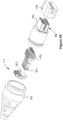
- the sensor 100 comprises a circuit board 102 which is for instance a printed circuit board (PCB) as known to a person skilled in the art.
- the circuit board 102 carries electronic components (not shown in this Figure) and transducer elements, such as a sensor coil in case the sensor 100 is an inductive proximity switch.
- a housing 104 encompasses the circuit board 102 and the components assembled thereon.
- an interface element 106 is mounted on the circuit carrier 102.
- the interface element 106 is electrically connected to the circuit carrier 102 by means of at least one inner contact 108.
- a plurality of inner contacts 108 are provided at the interface element 106, each of them being connected to a connecting interface 110.
- the connecting interface 110 is formed to be connected either with a peripheral plug connector 112 as shown in Fig. 1 or to a peripheral lead connector 114 as shown in Fig. 2 .
- the peripheral plug connector 112 can be formed to comply to the M12 5-position male connector according to the standard " Connectors for electronic equipment- Product requirements - Part 2-101: Circular connectors - Detail specification for M12 connectors with screw-locking" (IEC 61076-2-101:2012 ).
- a respective thread 116 for mechanically fixing the belonging mating connector is provided at the outside of a plastic cap 118.
- Locking means 120 are provided for mechanically fixing the peripheral connector 112 at the interface element 106 and therefore also at the PCB 102.
- the locking means 120 comprise a ring-shaped or hook-shaped snap-in connector. According to an example, this snap-fit connection does not have to be releasable after the peripheral connector has been assembled.
- the connecting interface 110 between the interface element 106 and the peripheral connector 112 or 114 is advantageously formed by a press-fit connection.
- the electrical connection between the interface element 106 and conductive tracks on the PCB 102 may for instance be established by means of reflow soldering.
- the interface element 106 can be formed as an SMD (surface mount device) component.
- SMD surface mount device
- the PCB 102 is mounted within an M12, M18, or M30 metal housing 104.
- a metal housing has the advantage that the electronic circuitry inside the housing 104 is protected against disturbing signals from the outside.
- Forming the housing 104 from two separate parts, namely an elongated metal shell 122 and a separate plastic cap 118, has the advantage that more complicated geometries for display and control elements can easily be combined with a shielding structure.
- the plastic cap 118 may for instance be formed as an injection molded part.
- Fig. 2 shows the same electronic component 100 which in contrast to the arrangement of Fig. 1 is not equipped with a peripheral plug connector 112, but with the peripheral lead connector 114.
- This different peripheral connector 114 carries a cable 124, and the sensor 100 therefore forms a so-called pigtail.
- the other end of the cable 124 may carry any suitable connector for contacting an external device (not shown in the Figures).
- the cable 124 may be a flat flexible cable, a coaxial cable, or any other electrical lead as required for contacting the external device.
- Figures 3 to 6 illustrate an example of an assembly method using an electrical connector kit according to an example.
- the circuit carrier 102 is equipped with an interface element 106.
- the inner contacts 108 are connected to electrical leads on the circuit carrier 102 for instance by means of reflow soldering.
- the printed circuit board 102 with the assembled interface element 106 is inserted into an essentially cylindrical metal shell 122 in a direction 126 along a longitudinal axis of the electronic component.
- the metal shell 122 has suitable guiding means (not shown in the Figures) for guiding and holding the PCB 102.
- a plastic cap 118 is inserted along the same direction 126 corresponding to the longitudinal axis of the electronic component.
- the plastic end cap 118 comprises a circumferential shoulder 128 for interacting with the locking means 120 of the peripheral connectors 112, 114.
- Fig. 6 shows the point in the assembly procedure when it is determined whether the electronic component 100 is equipped with the peripheral plug connector 112 or with the peripheral lead connector 114.
- the electrical connector kit comprises in addition to the interface element 106 also a set of at least one first and second peripheral connector 112, 114 which selectively can be connected to the interface element 106. As shown in the drawing, either a plug connector 112 or a lead connector 114 having a cable 124 can be attached to the interface element 106.
- peripheral connector 112, 114 is inserted along the longitudinal axis of the electronic component 100.
- a circumferential snap-fit element is provided as locking means 120 and engages with the shoulder 128 at the end cap 118 in an essentially irreversible manner.
- other peripheral connectors can be part of the electrical connector kit. For instance, means for a wireless connection, a plug connector socket, or another type of pin connector can be provided.
- peripheral connectors 112, 114 are equipped with press-fit contacts 130 that connect the respective peripheral connector 112, 114 to the connecting interface 110 of the interface element 106.
- press-fit contacts 130 can be used instead of the press-fit contacts 130.
- connection between the respective peripheral connector 112, 114 and the plastic end cap 118 can be designed in a way that the housing 104 is closed in a watertight and dustproof way. Alternatively, an additional casting step may also be performed for sealing the arrangement.
- FIG. 7 A further advantageous example will be described with reference to Figures 7 to 20 .
- This example mainly differs from the previous example in that an interface element 106 is first connected to each of the peripheral connectors 112, 114, and that the connection between the interface element 106 and the circuit carrier 102 is established in the same step when assembling the peripheral connectors 112, 114.
- This example has the advantage that firstly the amount of lose parts belonging to the electrical connector kit is reduced and that secondly the proprietary components belonging to the harnessing and peripheral contacts are introduced into the process of fabricating an electronic sensor component even later in the process sequence.
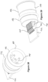
- Figures 7 to 10 show a peripheral plug connector 112 with an attached interface element 106.
- the interface element 106 is formed to engage with a PCB 102 in a clamping manner.
- the interface element 106 comprises spring contacts 132 which engage with contact areas (not shown in the Figures) provided on the printed circuit board 102.
- a snap-fit projection 134 is formed at the outside of the peripheral plug connector 112 for engaging with a belonging recess or shoulder provided at the sensor housing. Moreover, a ring-shaped gasket 136 seals the mechanical interface between the housing and the inserted peripheral plug connector 112 in the final mounted state.
- the spring contacts 132 are pushed over the printed circuit board 102 and establish an electrical contact due to the spring forces of the contact 132. These forces mainly are oriented across to the insertion direction 126.
- electrically insulating material can enter between the spring contacts 132 and the printed circuit board 102, thereby deteriorating the quality of the electrical contact. Consequently, the interface element 106 comprises a cover 138 for protecting the spring contacts 132 against the ingress of the cast resin.
- the cover 138 is fabricated from an elastic material, so that it is in tight contact with the PCB 102 before the cast resin is filled in.
- Figures 11 and 12 show the contact area of the interface element 106 without the cover 138.
- Fig. 13 shows an exploded view of the components forming the arrangement of Fig. 7 .
- the interface element 106 comprises spring contacts 132 which are assembled in the contact carrier 140.
- the spring contacts 132 are connected to an intermediate circuit board 142.
- the intermediate circuit board 142 has metallized contact openings 144 (vias) for receiving the spring contacts 132.
- the intermediate circuit board 142 is provided with a second plurality of metallized openings 146 (vias) which receive the plug connector pins 148 of the peripheral plug connector 112.
- Conducting paths are provided in the intermediate circuit board 142 that interconnect the vias 144, 146 and thereby electrically connect the spring contacts 132 with the belonging connector pins 148.
- the gasket 136 (which is to be arranged in a groove 150) seals the interface between the housing and the interface element 106.
- Fig. 14 to 17 show the belonging peripheral lead connector that belongs to the same connector kit as the plug connector 112 shown in Figures 7 to 13 .
- the interface towards the PCB 102 is identical and shows spring contacts 132 that contact the PCB 102 by clamping it from two sides at the edge.
- An elastic protective cover 138 is provided for preventing that casting resin is drawn by capillary forces into the minute gap between the PCB 102 and the spring contacts 132.
- the peripheral lead connector 114 comprises a plurality of electrically insulated wires 152 with a conductive core.
- the wires 152 may either be attached to the peripheral lead connector 114 as single leads or may form a ribbon cable.
- an arrangement with an intermediate circuit board 142 as shown in Figures 13 may also be used for fabricating the peripheral lead connector 114 of Figures 14 and 15 , it is even more efficient but outside the scope of the invention to directly connect the wires 152 to the spring contacts 132.
- the spring contacts 132 have insulation displacement terminations 154 for cutting the insulation of the wires 152 and electrically connecting the conductive cores of the wires 152.
- a further peripheral lead connector 114 with an attached interface element 106 is depicted in Figures 18 to 20 .
- the outgoing cable 124 is protected by a tension relief 156.
- the tension relief 156 is formed of an elastic material and comprises a sealing rim 158 which can replace the gasket 136.
- Fig. 20 illustrates a further possibility, not according to the invention, of attaching the wires of the cable 124 to the spring contacts 132.
- the spring contacts have crimp regions 164 for attaching the individual wires of the cable.
- the ends of the wires (not shown in Fig. 20 ) are first stripped from their insulation and then crimped individually to one spring contact 132 each.
- the spring contacts 132 are then arranged in holder 162 and inserted into the contact carrier 140.
- the protective cover 138 and the tension release 156 are attached. This arrangement provides a combined peripheral plug connector 112 with an interface element 106.
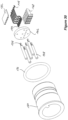
- Figures 21 to 32 illustrate a further advantageous example of a connector kit not according to the invention.
- Figures 21 to 27 relate to the peripheral lead connector 114 whereas Figures 28 to 30 show the corresponding peripheral plug connector 112.
- Figures 31 and 32 illustrate the assembly of the interface element 106.
- the wires 152 are attached by means of crimp connections 164 to the peripheral lead connector 114.
- the interface element 106 comprises inner contacts 108 that are soldered to the respective contact pads 166 provided at the PCB 102.
- the interface element 106 comprises an electrically insulating body 168 and a plurality of inner contacts 108 that provide a connecting interface 110 for the peripheral plug connector 112.
- An electrically insulating housing 170 of the peripheral plug connector has receptacles 172 through which EON (eye-of-the-needle) contacts 174 can be inserted.
- Fig. 26 shows the arrangement before being plugged together.
- Fig. 27 illustrates in an exploded view how the interface element 106 contacts the peripheral lead connector 114 with its EON contacts 174.
- an intermediate circuit board 142 is provided within the housing 170 of the peripheral connector. Wires 152 are fixed by crimp connections 164 to further EON contacts 176.
- the interface element 106 is soldered to the PCB 102, same is mounted within a housing (as shown in Fig. 5 ).
- the peripheral lead connector 114 is assembled by attaching the wires 152 at the intermediate circuit board 142 contained within the housing 170.
- the peripheral lead connector 114 is connected to the EON contacts 174 by inserting the lead connector 114 partly into the housing 104.
- FIGS 28 to 30 depict the corresponding peripheral plug connector 112.
- the construction of the plug connector 112 is similar to the design of the lead connector 114, with the exception that the housing is formed to hold plug connector pins 148 which are connected to an intermediate circuit board 142 by EON contacts 178.
- the connector housing 180 of the peripheral connector 112 has identical receptacles 172 for receiving the contacts 174 of the interface element 106.
- a suitable wiring provided within the intermediate circuit board 142 provides the connection between the inner contacts 108 and the pins 148.
- Fig. 31 and 32 finally, illustrate the fabrication of the interface element 106 with solderable inner contacts 108 and eye-of-the-needle contacts 174 at the connecting interface 110.
- the EON contacts 174 are fabricated as one single part with the inner contacts 108. These contacts are then arranged in an electrically insulating body 182.
- a cover 182 is mounted on the body 168 in order to fix the contact at the body and an ultrasonic welding step (illustrated by the arrow 184) connects the cover 182 to the body 168.
- An electrical connector kit for a circuit carrier 102 comprises at least one interface element 106 and at least one of the peripheral plug connector 112 and the peripheral lead connector 114. Consequently, when assembling an electronic component such as an inductive proximity switch, the decision whether a lead connector or a plug connector has to be mounted can be made towards the end of the assembly process. Is clear for a person skilled in the art that further peripheral connectors may of course also be provided with the electrical connector kit.
Landscapes
- Engineering & Computer Science (AREA)
- Microelectronics & Electronic Packaging (AREA)
- Manufacturing & Machinery (AREA)
- Mechanical Engineering (AREA)
- Details Of Connecting Devices For Male And Female Coupling (AREA)
- Coupling Device And Connection With Printed Circuit (AREA)
Description
- The present invention relates to an electrical connector kit for an electronic component and in particular for an inductive proximity sensor. Furthermore, the present invention relates to an assembly method for fabricating such an electronic component.
- The principles according to the present invention can be used advantageously for inductive sensors, and especially for proximity sensors. Inductive sensors are well known in the art and usually comprise a coil that is wound around a ferrite core and is used to form an oscillator. The inductive proximity sensor comprises a circuit board which is equipped with integrated circuits, for instance an electronic analyzing unit and an amplifying circuit. When a metallic object approaches the sensor, the oscillator is detuned and thus a signal in response to the approaching object can be generated. Such inductive proximity sensors are components fabricated in mass production and therefore the assembly has to be simple and cost-efficient.
- Typically, all components of the sensor are integrated within an elongated housing: The sensor coil is arranged at a front end of the sensor, whereas a peripheral contact element for connecting the sensor to external electronic components, i. e. a plug connector or an electrical lead, is arranged at the opposing back end of the sensor. A circuit carrier, usually a printed circuit board (PCB), carries the sensor electronics and is electrically connected to the peripheral contact element.
- There exist different concepts for equipping industrial sensors with a plug connector forming the peripheral contact element. A conventional plug connector is screwed or pressed into the housing and can then be connected to the PCB by means of electrically conductive leads which are manually soldered. Alternatively, a flexible printed circuit board can be soldered directly to the plug connector. Finally, a conventional plug connector can be assembled with a cable and an edge connector which is connected to the PCB. In particular the latter variant has the disadvantage that it needs a lot of space.
- It is further known to directly assemble the plug connector on the PCB and mount the PCB with the plug connector in a housing, so that the plug connector stays accessible via a suitable opening in the housing.
- According to a further conventional arrangement, a plurality of contact pins are assembled individually on the PCB and allowed to extend to the outside through a respective support structure in the housing.
- Finally, it is known to form a plug connector at the housing by means of an overmolding technique and to contact the PCB by means of a lead frame which is pressed-in or soldered to the PCB.
-
EP 1 398 878 A2 discloses a proximity sensor with a pin connector as peripheral connector. The connector has a conductive terminal assembly including a plug-adaptable conductive terminal electrically connected with a circuit assembly and a pin holder for holding the conductive terminal. The terminal assembly is sized to be able to be inserted from the front-end side of an outer shell case. A cylindrical holding member has openings at both ends to enable the conductive terminal assembly to be inserted, a joint to position the conductive terminal assembly to itself, and is fixed from the rear-end side of the outer shell case. In addition, the detection coil assembly and the conductive terminal assembly are electrically connected with each other via a flexible connection member. - Dixon, D. et al.: "The inductive prox: An old sensor with new wrinkles", CONTROL SOLUTIONS, PENNWELL PUBLISHING, TULSA, OK, US, vol. 62, no. 10, 31 October 1989 (1989-10-31), pages 55 - 58, XP000072564, ISSN: 1074-2328, gives an overview over inductive proximity sensors in general.
-
GB 2511389 A -
EP 2 278 669 A2 discloses a portable power supply adapter comprising a casing, a mains power supply cable extending from the casing for connection to a mains power supply, and a portable computer power supply cable extending from the casing for connection to a portable computer. The casing includes power supply circuitry, the casing having an upwardly facing surface, the surface including a plurality of sockets, each adapted to receive a portable electric device and arranged so that a plurality of portable electric devices may be charged from the mains power supply directly whether or not a portable computer is connected to the portable computer power supply cable for charging. -
US 2010/003857 A1 discloses an electrical connector assembly which includes a first and a second connector each including an insulating housing and a plurality of terminals retained in the housing. The housing has a front mating portion, a rear face, and a pair of first retaining portions at opposite ends of the rear face of the insulating housing. The terminals include leg portions extending out of the rear face of the housing. A receiving cavity is defined between the pair of retaining portions of the first connector. A transition board is vertically received in the receiving cavity of the first connector and the two pairs of retaining portions are engaged with each other to assembly the two connectors together. - Some applications require that the sensor is equipped with a cable of a suitable length, a so-called pigtail, instead of a plug connector. Such a cable can firstly be soldered manually to the printed circuit board. Secondly, the cable can be provided with an edge connector which is a rather space consuming concept. Conventional cable connections achieve a sealed encapsulation of the sensor components as well as the necessary strain relief by providing an additional overmolding step. Alternatively, a cable gland (also called PG, Panzergewinde, threaded fitting) is often used for providing sealing and strain relief.
- When fabricating such an inductive sensor, it is desirable to introduce the distinction concerning the particular peripheral contact element at a point within the assembly process as late as possible and preferably without manual soldering steps. The object underlying the present invention therefore is to provide an electrical connector kit for a circuit carrier that provides a particularly robust and reliable electrical contacting of the circuit carrier and whereby the assembly of a plug connector or a cable is delayed to an assembly step late in the fabrication process.
- This object is solved by the subject matter of the independent claims. Advantageous embodiments of the present invention are the subject matter of several dependent claims.
- Enabling disclosure can be found, for example, in
Figs. 1 to 6 .Figures 14 to 20 are useful for understanding the invention. - The present invention is based on the idea that by providing an electrical connector kit for a circuit carrier with at least one interface element which is attachable to the circuit carrier and has at least one inner contact for contacting at least one electrically conductive lead on the circuit carrier and further comprises an electrically connecting interface for contacting a peripheral connector, the decision on the particular peripheral connector can be postponed until one of the very last fabrication steps. According to the present invention, the kit comprises a set of at least one first and second peripheral connector each being connectable to the connecting interface of the interface element. The first and second peripheral connectors are characterized by different peripheral contact elements, such as a plug connector or an electrical lead, for contacting an external electronic component. For connecting the interface element to the circuit carrier, reliable automated techniques can be used. Hence, the connection between the circuit board and the peripheral connector is much more reliable than manually soldered connections.
- According to an advantageous example, the peripheral contact region of the first peripheral connector comprises a plug connector, for instance a male plug connector which can be connected to a mating female plug connector belonging to an external electronic component. The second peripheral connector may comprise as its peripheral contact element an electrical lead for forming a pigtail. Thus, all requirements regarding a particular type of peripheral contact element can easily be fulfilled.
- According to an example, the interface element can either be provided as a part separate from the first and second peripheral connectors, or one interface element can be provided for each of the first and second peripheral connectors. When designing the interface element as a separate part, same can for instance be fabricated as a surface mount device (SMD) component which is mounted directly on the printed circuit board before assembling the printed circuit board within the housing. Consequently, a particularly well-defined and robust connection can be established between the interface element and the PCB.
- Alternatively, each of the first and second peripheral connectors can be provided with an interface element. Such a construction is for instance advantageous in combination with an edge clamping electrical contact between the interface element and the PCB. For this variant the interface element is assembled with the respective first and second peripheral connectors already when compiling the electrical connector kit according to an example. A further advantage of this construction can be seen in the fact that less separate parts have to be stockpiled and handled at the facility where the sensors are assembled.
- In order to securely fix the first or second peripheral connector at the interface element and/or the circuit carrier, locking means can be provided at the peripheral connectors. The locking means can for instance comprise a snap-fit connection. According to an example, this snap-fit connection does not necessarily have to be detachable because once the sensor is assembled, same usually needs not be disassembled again. Advantageously, the snap-fit connection is established between a snap-fit hook arranged at the peripheral connector and a mating recess provided at the housing of the sensor.
- The interface element can be attached to the circuit carrier in various different ways. A particularly space saving arrangement can be achieved by forming the interface element as a surface mount device (SMD) component which is connected to the circuit carrier for instance by means of reflow soldering. Moreover, the soldered connection provides a particularly robust and low ohmic electrical contact. Alternatively, the interface element may also be attached to the printed circuit board by means of the press-fit connection. Furthermore, when pre-assembling the interface element with each of the first and second peripheral connectors, a particularly simple and reliable way of connecting the interface element to the circuit carrier is to provide electrically conductive spring contacts for being connected to contacts arranged at an edge of the circuit carrier by means of a force fit. By providing respective guiding means, a correct mating of the interface element and the circuit carrier can be ensured.
- According to an example, sealing means can be provided at the peripheral connectors so that a housing of the electronic circuitry is closed in a watertight and dustproof way after the peripheral connector is assembled. Consequently, no overmolding ("potting") is mandatory anymore. However, for certain applications it can still be useful to fill the housing with a casting resin. In this case and when using spring contacts, casting resin might enter between the spring contact and the circuit carrier, thereby deteriorating the electrical contact. It could be shown that this effect can be avoided by providing a protective cover at the interface element that protects the inner contacts against the intrusion of potting material.
- The advantages of an example may best be used for an electronic component having a housing with an essentially cylindrical shell that at least partly encompasses the circuit carrier. The first and second peripheral connectors can be formed as a cover to close the shell, so that the electronic circuitry is effectively protected against the ingress of moisture and dust. Moreover, the cylindrical shell may at least partly be formed from an electrically conductive material, for instance metal, so that it provides a shielding of the sensor electronics against interfering signals.
- The cylindrical shell may further comprise an additional electrically insulating end cap for receiving the first or second peripheral connector. Such an end cap could contain sensor specific display and input means, for instance light emitting diodes, potentiometers, and/or push buttons.
- A method for assembling an electronic component according to an example comprises the step of attaching an interface element to a circuit carrier, so that at least one inner contact is contacting at least one electrically conductive lead on said circuit carrier, said interface element further comprising an electrically connecting interface for contacting a peripheral connector. The method further comprises the step of connecting either the first or the second peripheral connector to said connecting interface, wherein the first and second peripheral connectors have peripheral contact elements for contacting an external electronic component which differ from each other. In particular, either a plug connector or an electrical lead can thus be attached to the electronic component at an instant towards the end of the assembly process.
- The sequence of these two steps according to an example depends on the particular example of the interface element. In particular, for an interface element that is formed as an SMD component or is equipped with press-fit pins, the interface element has to be mounted at the circuit carrier before attaching the peripheral connector. On the other hand, for the example of a clamping spring contact at the interface element it is advantageous to provide such an interface element at each peripheral connector before mounting same at the circuit carrier.
- In any case, the choice what sort of peripheral connector is to be mounted at the sensor component can be postponed until the very last assembly steps.
- In the foregoing, reference was always made to using the electrical connector kit with sensors and in particular with inductive proximity sensors. However, it is apparent for a person skilled in the art that the idea according to an example may also be used for any other kind of sensors or generally to other electronic components comprising circuit carriers having the need of peripheral contact elements for connecting the electronic component to external electronic components.
- FIG. 1
- shows schematically a sectional view of an inductive proximity sensor with a peripheral plug connector according to an example;
- FIG. 2
- shows schematically a sectional view of an inductive proximity sensor with a peripheral pigtail lead according to an example;
- FIG. 3
- shows a first assembly step for assembling the arrangement according to
Figures 1 and 2 ; - FIG. 4
- shows a further assembly step for assembling the arrangement according to
Figures 1 and 2 ; - FIG. 5
- shows a further assembly step for assembling the arrangement according to
Figures 1 and 2 ; - FIG. 6
- shows a further assembly step for assembling the arrangement according to
Figures 1 and 2 ; - FIG. 7
- shows a perspective view of a peripheral plug connector and an interface element according to the invention;
- FIG. 8
- shows the arrangement of
Fig. 7 rotated by 90°; - FIG. 9
- shows schematically the position of the circuit carrier for the arrangement of
Fig. 7 ; - FIG. 10
- shows the arrangement of
Fig. 9 rotated by 180°; - FIG 11
- shows the arrangement of
Fig. 7 without the protective cover; - FIG. 12
- shows the arrangement of
Fig. 11 in a rotated position; - FIG. 13
- shows a perspective exploded view of the peripheral plug connector and interface element according to
Fig. 7 ; - FIG. 14
- shows a perspective view of a peripheral pigtail connector and an interface element according to the invention;
- FIG. 15
- shows the arrangement of
Fig. 14 in a rotated position; - FIG. 16
- shows an arrangement of
Fig. 14 in an exploded view, this arrangement being outside the invention; - FIG. 17
- shows a further partly exploded view of an arrangement of
Fig. 14 , this arrangement being outside the invention; - FIG. 18
- shows a perspective view of a peripheral cable connector and an interface element according to an example;
- FIG. 19
- shows the arrangement of
Fig. 18 rotated by 180°; - FIG. 20
- shows an arrangement of
Fig. 18 in an exploded view, this arrangement being outside the invention; - FIG. 21
- shows a perspective view of a peripheral cable connector with an interface element according to a further example not according to the invention;
- FIG. 22
- shows the arrangement of
Fig. 21 rotated by 90°; - FIG. 23
- shows the arrangement of
Fig. 21 in another rotated view; - FIG. 24
- shows a perspective view of a peripheral plug connector according to a further example not according to the invention;
- FIG. 25
- shows an interface element to be connected with the peripheral plug connected according to
Fig. 24 ; - FIG. 26
- shows the interface element of
Fig. 25 and the belonging peripheral plug connector ofFig. 25 before being connected; - FIG. 27
- shows the arrangement of
Fig. 21 in an exploded view; - FIG. 28
- shows an example of a peripheral plug connector using the interface element according to
Fig. 25 ; - FIG. 29
- shows the arrangement of
Fig. 28 rotated by 90°; - FIG. 30
- shows the arrangement of
Fig. 28 in an exploded view; - FIG. 31
- shows an assembly step for fabricating the interface element of
Fig. 25 ; - FIG. 32
- shows a final step for fabricating the interface element of
Fig. 25 . - Examples will now be explained in more detail with reference to the Figures.
- Referring now to
Fig. 1 , anelectronic component 100, in particular a sensor, is shown which is assembled using an electrically connector kit according to an example. Thesensor 100 comprises acircuit board 102 which is for instance a printed circuit board (PCB) as known to a person skilled in the art. Thecircuit board 102 carries electronic components (not shown in this Figure) and transducer elements, such as a sensor coil in case thesensor 100 is an inductive proximity switch. Ahousing 104 encompasses thecircuit board 102 and the components assembled thereon. - According to an example, an
interface element 106 is mounted on thecircuit carrier 102. Theinterface element 106 is electrically connected to thecircuit carrier 102 by means of at least oneinner contact 108. In the present case, a plurality ofinner contacts 108 are provided at theinterface element 106, each of them being connected to a connectinginterface 110. - The connecting
interface 110 is formed to be connected either with aperipheral plug connector 112 as shown inFig. 1 or to a peripherallead connector 114 as shown inFig. 2 . Of course, any other suitable alternative of how the peripheral connector can be formed is also covered by the present invention. For instance, theperipheral plug connector 112 can be formed to comply to the M12 5-position male connector according to the standard "Connectors for electronic equipment- Product requirements - Part 2-101: Circular connectors - Detail specification for M12 connectors with screw-locking" (IEC 61076-2-101:2012). Arespective thread 116 for mechanically fixing the belonging mating connector is provided at the outside of aplastic cap 118. - Locking means 120 are provided for mechanically fixing the
peripheral connector 112 at theinterface element 106 and therefore also at thePCB 102. As schematically shown inFig. 1 , the locking means 120 comprise a ring-shaped or hook-shaped snap-in connector. According to an example, this snap-fit connection does not have to be releasable after the peripheral connector has been assembled. - The connecting
interface 110 between theinterface element 106 and theperipheral connector interface element 106 and conductive tracks on thePCB 102 may for instance be established by means of reflow soldering. In particular, theinterface element 106 can be formed as an SMD (surface mount device) component. However, it is clear for a person skilled in the art that also other suitable ways of contacting thePCB 102 can be employed at this point. - According to the example shown in
Figures 1 to 6 , thePCB 102 is mounted within an M12, M18, orM30 metal housing 104. Such a metal housing has the advantage that the electronic circuitry inside thehousing 104 is protected against disturbing signals from the outside. Forming thehousing 104 from two separate parts, namely anelongated metal shell 122 and a separateplastic cap 118, has the advantage that more complicated geometries for display and control elements can easily be combined with a shielding structure. Theplastic cap 118 may for instance be formed as an injection molded part. -
Fig. 2 shows the sameelectronic component 100 which in contrast to the arrangement ofFig. 1 is not equipped with aperipheral plug connector 112, but with the peripherallead connector 114. This differentperipheral connector 114 carries acable 124, and thesensor 100 therefore forms a so-called pigtail. It has to be noted that the other end of thecable 124 may carry any suitable connector for contacting an external device (not shown in the Figures). Thecable 124 may be a flat flexible cable, a coaxial cable, or any other electrical lead as required for contacting the external device. -
Figures 3 to 6 illustrate an example of an assembly method using an electrical connector kit according to an example. As shown inFig. 3 , according to a first example, thecircuit carrier 102 is equipped with aninterface element 106. Theinner contacts 108 are connected to electrical leads on thecircuit carrier 102 for instance by means of reflow soldering. As shown inFig. 4 , the printedcircuit board 102 with the assembledinterface element 106 is inserted into an essentiallycylindrical metal shell 122 in adirection 126 along a longitudinal axis of the electronic component. Themetal shell 122 has suitable guiding means (not shown in the Figures) for guiding and holding thePCB 102. - In a next step (see
Fig. 5 ) aplastic cap 118 is inserted along thesame direction 126 corresponding to the longitudinal axis of the electronic component. As will become more apparent from the following Figures, theplastic end cap 118 comprises acircumferential shoulder 128 for interacting with the locking means 120 of theperipheral connectors -
Fig. 6 shows the point in the assembly procedure when it is determined whether theelectronic component 100 is equipped with theperipheral plug connector 112 or with the peripherallead connector 114. According to an example, the electrical connector kit comprises in addition to theinterface element 106 also a set of at least one first and secondperipheral connector interface element 106. As shown in the drawing, either aplug connector 112 or alead connector 114 having acable 124 can be attached to theinterface element 106. - The respective
peripheral connector electronic component 100. A circumferential snap-fit element is provided as locking means 120 and engages with theshoulder 128 at theend cap 118 in an essentially irreversible manner. In addition to theperipheral connectors Fig. 6 , of course also other peripheral connectors can be part of the electrical connector kit. For instance, means for a wireless connection, a plug connector socket, or another type of pin connector can be provided. - In the example shown in
Fig. 6 , theperipheral connectors fit contacts 130 that connect the respectiveperipheral connector interface 110 of theinterface element 106. However, also abutting spring contacts can be used instead of the press-fit contacts 130. - The connection between the respective
peripheral connector plastic end cap 118 can be designed in a way that thehousing 104 is closed in a watertight and dustproof way. Alternatively, an additional casting step may also be performed for sealing the arrangement. - A further advantageous example will be described with reference to
Figures 7 to 20 . This example mainly differs from the previous example in that aninterface element 106 is first connected to each of theperipheral connectors interface element 106 and thecircuit carrier 102 is established in the same step when assembling theperipheral connectors - This example has the advantage that firstly the amount of lose parts belonging to the electrical connector kit is reduced and that secondly the proprietary components belonging to the harnessing and peripheral contacts are introduced into the process of fabricating an electronic sensor component even later in the process sequence.
-
Figures 7 to 10 show aperipheral plug connector 112 with an attachedinterface element 106. According to this particular example, theinterface element 106 is formed to engage with aPCB 102 in a clamping manner. To this end, theinterface element 106 comprisesspring contacts 132 which engage with contact areas (not shown in the Figures) provided on the printedcircuit board 102. - A snap-
fit projection 134 is formed at the outside of theperipheral plug connector 112 for engaging with a belonging recess or shoulder provided at the sensor housing. Moreover, a ring-shapedgasket 136 seals the mechanical interface between the housing and the insertedperipheral plug connector 112 in the final mounted state. - The
spring contacts 132 are pushed over the printedcircuit board 102 and establish an electrical contact due to the spring forces of thecontact 132. These forces mainly are oriented across to theinsertion direction 126. However, when overmolding thecircuit carrier 102 by filling a cast resin into the housing (not shown in the Figures), electrically insulating material can enter between thespring contacts 132 and the printedcircuit board 102, thereby deteriorating the quality of the electrical contact. Consequently, theinterface element 106 comprises acover 138 for protecting thespring contacts 132 against the ingress of the cast resin. Preferably, thecover 138 is fabricated from an elastic material, so that it is in tight contact with thePCB 102 before the cast resin is filled in. -
Figures 11 and 12 show the contact area of theinterface element 106 without thecover 138. -
Fig. 13 shows an exploded view of the components forming the arrangement ofFig. 7 . In particular, theinterface element 106 comprisesspring contacts 132 which are assembled in thecontact carrier 140. In order to form a connectinginterface 110 towards theperipheral plug connector 112, thespring contacts 132 are connected to anintermediate circuit board 142. Theintermediate circuit board 142 has metallized contact openings 144 (vias) for receiving thespring contacts 132. Moreover, theintermediate circuit board 142 is provided with a second plurality of metallized openings 146 (vias) which receive the plug connector pins 148 of theperipheral plug connector 112. Conducting paths (not shown in the Figures) are provided in theintermediate circuit board 142 that interconnect thevias spring contacts 132 with the belonging connector pins 148. - As already mentioned, the gasket 136 (which is to be arranged in a groove 150) seals the interface between the housing and the
interface element 106. -
Fig. 14 to 17 show the belonging peripheral lead connector that belongs to the same connector kit as theplug connector 112 shown inFigures 7 to 13 . - As can be seen in
Figures 14 and 15 , the interface towards thePCB 102 is identical and showsspring contacts 132 that contact thePCB 102 by clamping it from two sides at the edge. An elasticprotective cover 138 is provided for preventing that casting resin is drawn by capillary forces into the minute gap between thePCB 102 and thespring contacts 132. - In contrast to the
peripheral plug connector 112 shown inFigures 7 to 13 , the peripherallead connector 114 comprises a plurality of electrically insulatedwires 152 with a conductive core. Thewires 152 may either be attached to the peripherallead connector 114 as single leads or may form a ribbon cable. Although an arrangement with anintermediate circuit board 142 as shown inFigures 13 may also be used for fabricating the peripherallead connector 114 ofFigures 14 and 15 , it is even more efficient but outside the scope of the invention to directly connect thewires 152 to thespring contacts 132. This example not according to the invention is illustrated inFigures 16 and 17 . In particular, thespring contacts 132 haveinsulation displacement terminations 154 for cutting the insulation of thewires 152 and electrically connecting the conductive cores of thewires 152. - A further peripheral
lead connector 114 with an attachedinterface element 106 is depicted inFigures 18 to 20 . According to this example, theoutgoing cable 124 is protected by atension relief 156. Furthermore, thetension relief 156 is formed of an elastic material and comprises a sealingrim 158 which can replace thegasket 136. -
Fig. 20 illustrates a further possibility, not according to the invention, of attaching the wires of thecable 124 to thespring contacts 132. According to this example, the spring contacts havecrimp regions 164 for attaching the individual wires of the cable. For fabricating the arrangement shown inFig. 18 , the ends of the wires (not shown inFig. 20 ) are first stripped from their insulation and then crimped individually to onespring contact 132 each. Thespring contacts 132 are then arranged inholder 162 and inserted into thecontact carrier 140. Next, theprotective cover 138 and thetension release 156 are attached. This arrangement provides a combinedperipheral plug connector 112 with aninterface element 106. -
Figures 21 to 32 illustrate a further advantageous example of a connector kit not according to the invention.Figures 21 to 27 relate to the peripherallead connector 114 whereasFigures 28 to 30 show the correspondingperipheral plug connector 112.Figures 31 and 32 illustrate the assembly of theinterface element 106. - As shown in
Fig. 21 , thewires 152 are attached by means ofcrimp connections 164 to the peripherallead connector 114. Theinterface element 106 comprisesinner contacts 108 that are soldered to therespective contact pads 166 provided at thePCB 102. As becomes more apparent fromFig. 25 , theinterface element 106 comprises an electrically insulatingbody 168 and a plurality ofinner contacts 108 that provide a connectinginterface 110 for theperipheral plug connector 112. An electrically insulatinghousing 170 of the peripheral plug connector hasreceptacles 172 through which EON (eye-of-the-needle)contacts 174 can be inserted.Fig. 26 shows the arrangement before being plugged together. -
Fig. 27 illustrates in an exploded view how theinterface element 106 contacts the peripherallead connector 114 with itsEON contacts 174. Similar to the example shown inFig. 13 , anintermediate circuit board 142 is provided within thehousing 170 of the peripheral connector.Wires 152 are fixed bycrimp connections 164 tofurther EON contacts 176. After theinterface element 106 is soldered to thePCB 102, same is mounted within a housing (as shown inFig. 5 ). The peripherallead connector 114 is assembled by attaching thewires 152 at theintermediate circuit board 142 contained within thehousing 170. Finally, the peripherallead connector 114 is connected to theEON contacts 174 by inserting thelead connector 114 partly into thehousing 104. -
Figures 28 to 30 depict the correspondingperipheral plug connector 112. The construction of theplug connector 112 is similar to the design of thelead connector 114, with the exception that the housing is formed to hold plug connector pins 148 which are connected to anintermediate circuit board 142 byEON contacts 178. Theconnector housing 180 of theperipheral connector 112 hasidentical receptacles 172 for receiving thecontacts 174 of theinterface element 106. A suitable wiring provided within theintermediate circuit board 142 provides the connection between theinner contacts 108 and thepins 148. -
Fig. 31 and 32 , finally, illustrate the fabrication of theinterface element 106 with solderableinner contacts 108 and eye-of-the-needle contacts 174 at the connectinginterface 110. - Firstly, the
EON contacts 174 are fabricated as one single part with theinner contacts 108. These contacts are then arranged in an electrically insulatingbody 182. Acover 182 is mounted on thebody 168 in order to fix the contact at the body and an ultrasonic welding step (illustrated by the arrow 184) connects thecover 182 to thebody 168. - An electrical connector kit for a
circuit carrier 102 according to an example comprises at least oneinterface element 106 and at least one of theperipheral plug connector 112 and the peripherallead connector 114. Consequently, when assembling an electronic component such as an inductive proximity switch, the decision whether a lead connector or a plug connector has to be mounted can be made towards the end of the assembly process. Is clear for a person skilled in the art that further peripheral connectors may of course also be provided with the electrical connector kit.REFERENCE NUMERALS Reference Numeral Description 100 Electronic component 102 Circuit carrier (PCB) 104 Housing 106 Interface element 108 Inner contact 110 Connecting interface 112 Peripheral plug connector 114 Peripheral lead connector 116 Thread 118 Plastic end cap 120 Locking means 122 Metal shell 124 Cable 126 Inserting direction 128 Shoulder at end cap 130 Press- fit contact 132 Spring contact 134 Snap- fit projection 136 Ring-shaped gasket 138 Protective cover 140 Contact carrier 142 Intermediate circuit board 144 First metallized opening 146 Second metallized opening 148 Plug connector pins 150 Groove 152 Wire 154 Insulation displacement termination 156 Tension relief 158 Sealing rim 160 Crimp region 162 Holder 164 Crimp connection 166 Contact pad 168 Body of interface element 170 Housing of peripheral lead connector 172 Receptacle 174 EON contact of interface element 176 EON contact of peripheral connector 178 EON contact of pin 180 Housing of peripheral plug connector 182 Cover of interface element
Claims (10)
- Electrical connector kit for attaching one of at least a first or a second peripheral connector (112, 114) to a printed circuit board (102) of an inductive proximity sensor, said connector kit comprising:at least one interface element (106) which is attachable to said printed circuit board (102) for contacting at least one electrically conductive lead on said printed circuit board (102), said interface element (106) further comprising an electrically connecting interface (110) for contacting said at least one first or second peripheral connector (112, 114),
the connector kit being characterised in that it further comprises a set of at least one first and second peripheral connectors (112, 114), each having press-fit contacts (130) being connectable to said connecting interface (110),wherein, for contacting at least one external electronic component, said first and second peripheral connectors (112, 114) have peripheral contact elements which differ from each other, wherein the peripheral contact element of the first peripheral connector (112) comprises plug connector pins (148), and wherein the peripheral contact element of the second peripheral connector (114) comprises an electrical lead (152, 124) attached thereto, andwherein the interface element (106) comprises spring contacts (132) which engage with contact areas provided on the printed circuit board (102) in a clamping manner, and wherein said interface element (106) comprises a cover (138) for protecting said electrically conductive spring contacts (132) against ingress of cast resin. - Electrical connector kit according to claim 1, comprising one interface element (106) for each of the said first and second peripheral connectors (112, 114).
- Electrical connector kit according to claim 1, wherein said first and second peripheral connectors (112, 114) comprise a snap-fit projection (134) for mechanically securing the peripheral connectors (112, 114) in a mounted state.
- Electronic component (100) comprisingone printed circuit board (102), andan electrical connector kit according to one of the preceding claims,the spring contacts (132) of the interface element (106) engaging with contact areas provided on the printed circuit board (102) in a clamping manner, andthe press-fit contacts (130) of one of the first or the second peripheral connector (112, 114) being connected to said connecting interface (110) of the interface element (106) .
- Electronic component according to claim 4, wherein said printed circuit board (102) comprises at least one inductive proximity sensor.
- Electronic component according to one of the claims 4 or 5, further comprising a housing (104) that at least partly encompasses said printed circuit board (102).
- Electronic component according to claim 6, wherein said housing (104) comprises an essentially cylindrical shell (122, 118), and wherein said first and second peripheral connectors (112, 114) are formed as a cover to close said shell (122, 118).
- Electronic component according to claim 7, wherein said cylindrical shell (122, 118) comprises an electrically conductive shielding part (122) and an electrically insulating end cap (118) for receiving said first or second peripheral connector (112, 114).
- Method for assembling an electronic component according to one of the claims 4 to 8, the method comprising the following steps:attaching an interface element (106) to a printed circuit board (102), so that the spring contacts (132) of the interface element (106) engage with contact areas provided on said printed circuit board (102) in a clamping manner,said interface element (106) further comprising an electrically connecting interface (110) for contacting the at least one first or second peripheral connector (112, 114);connecting either the first or the second peripheral connector (112, 114) to said connecting interface (110), wherein said first and second peripheral connectors (112, 114) have peripheral contact elements for contacting an external electronic component which differ from each other.
- Method according to claim 9, wherein one interface element (106) is attached as a separate element to the printed circuit board (102) before mounting either the first or second peripheral connector (112, 114), or wherein one interface element (106) is attached to each of the first and second peripheral connectors (112, 114) before being mounted at the printed circuit board (102).
Priority Applications (5)
| Application Number | Priority Date | Filing Date | Title |
|---|---|---|---|
| EP15158971.0A EP3067992B1 (en) | 2015-03-13 | 2015-03-13 | Electrical connector kit, electronic component, and assembly method |
| PCT/EP2016/055382 WO2016146553A1 (en) | 2015-03-13 | 2016-03-11 | Electrical connector kit, electronic component, and assembly method |
| CN201680015513.7A CN107431306B (en) | 2015-03-13 | 2016-03-11 | Electric connector kit, electronic component and assembling method |
| JP2017547991A JP6472897B2 (en) | 2015-03-13 | 2016-03-11 | Electrical connector kit, electronic component, and assembly method |
| US15/703,159 US10403995B2 (en) | 2015-03-13 | 2017-09-13 | Electrical connector, electronic component, and assembly method |
Applications Claiming Priority (1)
| Application Number | Priority Date | Filing Date | Title |
|---|---|---|---|
| EP15158971.0A EP3067992B1 (en) | 2015-03-13 | 2015-03-13 | Electrical connector kit, electronic component, and assembly method |
Publications (2)
| Publication Number | Publication Date |
|---|---|
| EP3067992A1 EP3067992A1 (en) | 2016-09-14 |
| EP3067992B1 true EP3067992B1 (en) | 2024-04-03 |
Family
ID=52648938
Family Applications (1)
| Application Number | Title | Priority Date | Filing Date |
|---|---|---|---|
| EP15158971.0A Active EP3067992B1 (en) | 2015-03-13 | 2015-03-13 | Electrical connector kit, electronic component, and assembly method |
Country Status (5)
| Country | Link |
|---|---|
| US (1) | US10403995B2 (en) |
| EP (1) | EP3067992B1 (en) |
| JP (1) | JP6472897B2 (en) |
| CN (1) | CN107431306B (en) |
| WO (1) | WO2016146553A1 (en) |
Families Citing this family (5)
| Publication number | Priority date | Publication date | Assignee | Title |
|---|---|---|---|---|
| WO2018120774A1 (en) * | 2016-12-28 | 2018-07-05 | Guangdong Oppo Mobile Telecommunications Corp., Ltd. | Antenna device for mobile terminal and mobile terminal |
| DE102017105186B4 (en) * | 2017-03-10 | 2019-05-23 | Amphenol-Tuchel Electronics Gmbh | Circular connector socket for an attachable circuit board |
| DE102018216477B4 (en) * | 2018-09-26 | 2023-03-16 | Robert Bosch Gmbh | Steering device with a connector unit for electrically contacting a steering sensor unit |
| DE102019104881B4 (en) * | 2019-02-26 | 2020-12-10 | Pilz Gmbh & Co. Kg | Storage device for the mobile provision of data at a technical facility |
| US11456551B2 (en) | 2019-05-30 | 2022-09-27 | Raytheon Company | Spring pin connector for blind-mate coupling a sensor to an electronics assembly |
Citations (2)
| Publication number | Priority date | Publication date | Assignee | Title |
|---|---|---|---|---|
| US20100003857A1 (en) * | 2008-07-02 | 2010-01-07 | Hon Hai Precision Industry Co., Ltd. | Electrical connector assembly with a transition board |
| EP2278669A2 (en) * | 2009-07-21 | 2011-01-26 | Mr Eng Choon Low | Power supply adapter |
Family Cites Families (14)
| Publication number | Priority date | Publication date | Assignee | Title |
|---|---|---|---|---|
| DE2530157A1 (en) * | 1975-07-05 | 1977-02-03 | Bosch Gmbh Robert | ELECTRONIC CONTROL UNIT |
| JPH0526680Y2 (en) * | 1989-10-13 | 1993-07-06 | ||
| KR200252401Y1 (en) * | 1998-09-26 | 2001-12-28 | 윤종용 | Connector assembly |
| JP3058839U (en) * | 1998-11-02 | 1999-06-22 | 日邦ミシン株式会社 | Fabric roll-in guide |
| JP3844073B2 (en) * | 2002-09-13 | 2006-11-08 | オムロン株式会社 | Proximity sensor |
| JP2007066592A (en) * | 2005-08-30 | 2007-03-15 | Fujitsu General Ltd | Electronic equipment |
| US7335066B2 (en) * | 2005-12-16 | 2008-02-26 | James A. Carroll | Network connector and connection system |
| WO2008116224A1 (en) * | 2007-03-22 | 2008-09-25 | Stoneridge Control Devices, Inc. | Trailer tow connector assembly |
| TWM406822U (en) * | 2009-02-18 | 2011-07-01 | Molex Inc | Multi-plugging connector system |
| US8292670B2 (en) * | 2011-02-28 | 2012-10-23 | Honeywell International Inc. | Cable interface device |
| WO2012142606A2 (en) * | 2011-04-15 | 2012-10-18 | Hypertronics Corporation | High density electrical connector having a printed circuit board |
| CN102437491B (en) * | 2011-08-03 | 2014-04-02 | 华为机器有限公司 | Connection structure of circuit board and panel |
| GB2511389B (en) * | 2012-12-14 | 2016-04-06 | Sheng-Hsin Liao | Assembled connecting device with a protective sleeve |
| US9419391B2 (en) * | 2013-08-20 | 2016-08-16 | Panduit Corp. | Communication connector |
-
2015
- 2015-03-13 EP EP15158971.0A patent/EP3067992B1/en active Active
-
2016
- 2016-03-11 WO PCT/EP2016/055382 patent/WO2016146553A1/en active Application Filing
- 2016-03-11 JP JP2017547991A patent/JP6472897B2/en active Active
- 2016-03-11 CN CN201680015513.7A patent/CN107431306B/en active Active
-
2017
- 2017-09-13 US US15/703,159 patent/US10403995B2/en active Active
Patent Citations (2)
| Publication number | Priority date | Publication date | Assignee | Title |
|---|---|---|---|---|
| US20100003857A1 (en) * | 2008-07-02 | 2010-01-07 | Hon Hai Precision Industry Co., Ltd. | Electrical connector assembly with a transition board |
| EP2278669A2 (en) * | 2009-07-21 | 2011-01-26 | Mr Eng Choon Low | Power supply adapter |
Also Published As
| Publication number | Publication date |
|---|---|
| US20180006390A1 (en) | 2018-01-04 |
| US10403995B2 (en) | 2019-09-03 |
| EP3067992A1 (en) | 2016-09-14 |
| JP6472897B2 (en) | 2019-02-20 |
| WO2016146553A1 (en) | 2016-09-22 |
| CN107431306A (en) | 2017-12-01 |
| JP2018511913A (en) | 2018-04-26 |
| CN107431306B (en) | 2020-11-24 |
Similar Documents
| Publication | Publication Date | Title |
|---|---|---|
| US10403995B2 (en) | Electrical connector, electronic component, and assembly method | |
| US3961294A (en) | Connector having filter adaptor | |
| US11569611B2 (en) | Connector assembly with an intermediate insulating member and a potting material that fills a portion in an outer conductor more on the front side than on the front surface of the intermediate insulating member | |
| KR100811579B1 (en) | Receptacle type intermediate connector | |
| US7390197B2 (en) | Electronic device with integral connectors | |
| KR101471283B1 (en) | Electrical connector for use with a circuit board | |
| US20150072557A1 (en) | Plug connector having a ground band and an insert molded contact assembly | |
| US20080267617A1 (en) | Electrical connector and camera device having the same | |
| US9343835B2 (en) | Terminal and connector having the same | |
| CN111864458A (en) | Electrical connector | |
| US9385487B2 (en) | Active plug connector and method for assembling the same | |
| CN113067232B (en) | Method for manufacturing electric connector, electric connector and electronic device | |
| JP5787081B2 (en) | Connector device | |
| JP5473758B2 (en) | connector | |
| US7008273B2 (en) | Cable connector assembly and method of making the same | |
| JP2019216043A (en) | Inner conductor terminal, and terminal unit for coaxial line using inner conductor terminal | |
| US7980881B2 (en) | Connecting device and method of use | |
| KR101734834B1 (en) | Usb connector that allows easy mounting and manufacturing method thereof | |
| CN111129851A (en) | Electrical connector and connector assembly | |
| KR200472617Y1 (en) | Bending type micro Universal Serial Bus plug assembly for cable without Printed Circuit Board and soldering | |
| JP7282449B2 (en) | plugs and receptacles | |
| CN212277515U (en) | Electrical connector | |
| JP6032422B2 (en) | Photoelectric composite connector device | |
| US20220294167A1 (en) | Method for manufacturing data transmission apparatus and data transmission apparatus | |
| JP3357873B2 (en) | Fiber optic cable and audio or information equipment |
Legal Events
| Date | Code | Title | Description |
|---|---|---|---|
| PUAI | Public reference made under article 153(3) epc to a published international application that has entered the european phase |
Free format text: ORIGINAL CODE: 0009012 |
|
| AK | Designated contracting states |
Kind code of ref document: A1 Designated state(s): AL AT BE BG CH CY CZ DE DK EE ES FI FR GB GR HR HU IE IS IT LI LT LU LV MC MK MT NL NO PL PT RO RS SE SI SK SM TR |
|
| AX | Request for extension of the european patent |
Extension state: BA ME |
|
| STAA | Information on the status of an ep patent application or granted ep patent |
Free format text: STATUS: REQUEST FOR EXAMINATION WAS MADE |
|
| 17P | Request for examination filed |
Effective date: 20170224 |
|
| RBV | Designated contracting states (corrected) |
Designated state(s): AL AT BE BG CH CY CZ DE DK EE ES FI FR GB GR HR HU IE IS IT LI LT LU LV MC MK MT NL NO PL PT RO RS SE SI SK SM TR |
|
| STAA | Information on the status of an ep patent application or granted ep patent |
Free format text: STATUS: EXAMINATION IS IN PROGRESS |
|
| 17Q | First examination report despatched |
Effective date: 20170405 |
|
| RIN1 | Information on inventor provided before grant (corrected) |
Inventor name: SCHRETTLINGER, CHRISTIAN Inventor name: STRELOW, MARKUS Inventor name: BUECHLING, CHRIS Inventor name: WALLDORF, DANIEL Inventor name: BUSCEMI, CALOGERO MAURO Inventor name: WOLF, FRANK Inventor name: LAUB, MIKE Inventor name: BUCHMANN, ULRICH Inventor name: BURGER, STEFFEN |
|
| STAA | Information on the status of an ep patent application or granted ep patent |
Free format text: STATUS: EXAMINATION IS IN PROGRESS |
|
| STAA | Information on the status of an ep patent application or granted ep patent |
Free format text: STATUS: EXAMINATION IS IN PROGRESS |
|
| GRAP | Despatch of communication of intention to grant a patent |
Free format text: ORIGINAL CODE: EPIDOSNIGR1 |
|
| STAA | Information on the status of an ep patent application or granted ep patent |
Free format text: STATUS: GRANT OF PATENT IS INTENDED |
|
| RIC1 | Information provided on ipc code assigned before grant |
Ipc: H01R 12/72 20110101ALN20231127BHEP Ipc: H01R 12/58 20110101ALN20231127BHEP Ipc: H01R 13/627 20060101ALN20231127BHEP Ipc: H01R 13/504 20060101ALI20231127BHEP Ipc: B29C 45/14 20060101ALI20231127BHEP Ipc: H01R 31/06 20060101ALI20231127BHEP Ipc: H03K 17/95 20060101ALI20231127BHEP Ipc: H01R 13/66 20060101ALI20231127BHEP Ipc: H01R 13/514 20060101AFI20231127BHEP |
|
| INTG | Intention to grant announced |
Effective date: 20231213 |
|
| GRAS | Grant fee paid |
Free format text: ORIGINAL CODE: EPIDOSNIGR3 |
|
| GRAA | (expected) grant |
Free format text: ORIGINAL CODE: 0009210 |
|
| STAA | Information on the status of an ep patent application or granted ep patent |
Free format text: STATUS: THE PATENT HAS BEEN GRANTED |
|
| AK | Designated contracting states |
Kind code of ref document: B1 Designated state(s): AL AT BE BG CH CY CZ DE DK EE ES FI FR GB GR HR HU IE IS IT LI LT LU LV MC MK MT NL NO PL PT RO RS SE SI SK SM TR |
|
| REG | Reference to a national code |
Ref country code: GB Ref legal event code: FG4D |
|
| REG | Reference to a national code |
Ref country code: CH Ref legal event code: EP |
|
| REG | Reference to a national code |
Ref country code: DE Ref legal event code: R096 Ref document number: 602015088133 Country of ref document: DE |
|
| REG | Reference to a national code |
Ref country code: IE Ref legal event code: FG4D |