EP3062442B1 - Hybrid recursive active filtering with adaptive transfer function shaping capability - Google Patents
Hybrid recursive active filtering with adaptive transfer function shaping capability Download PDFInfo
- Publication number
- EP3062442B1 EP3062442B1 EP15156984.5A EP15156984A EP3062442B1 EP 3062442 B1 EP3062442 B1 EP 3062442B1 EP 15156984 A EP15156984 A EP 15156984A EP 3062442 B1 EP3062442 B1 EP 3062442B1
- Authority
- EP
- European Patent Office
- Prior art keywords
- digital
- feedback
- path
- filter
- loop
- Prior art date
- Legal status (The legal status is an assumption and is not a legal conclusion. Google has not performed a legal analysis and makes no representation as to the accuracy of the status listed.)
- Not-in-force
Links
Images


Classifications
-
- H—ELECTRICITY
- H03—ELECTRONIC CIRCUITRY
- H03H—IMPEDANCE NETWORKS, e.g. RESONANT CIRCUITS; RESONATORS
- H03H17/00—Networks using digital techniques
- H03H17/02—Frequency selective networks
- H03H17/0283—Filters characterised by the filter structure
- H03H17/0286—Combinations of filter structures
- H03H17/0289—Digital and active filter structures
-
- H—ELECTRICITY
- H03—ELECTRONIC CIRCUITRY
- H03H—IMPEDANCE NETWORKS, e.g. RESONANT CIRCUITS; RESONATORS
- H03H11/00—Networks using active elements
- H03H11/02—Multiple-port networks
- H03H11/04—Frequency selective two-port networks
- H03H11/12—Frequency selective two-port networks using amplifiers with feedback
- H03H11/126—Frequency selective two-port networks using amplifiers with feedback using a single operational amplifier
Definitions
- the present invention relates to hybrid recursive active filtering with adaptive transfer function shaping capability. More specifically, the present invention relates to a hybrid recursive active filter, a method of operating the same, and a computer program product for carrying out the method of operating the same.
- radio-frequency units like RF front-ends of communication apparatuses (such as e.g. base stations, base transceiver stations, and access nodes) do have to fulfill stringent requirements.
- RF front-ends of communication apparatuses such as e.g. base stations, base transceiver stations, and access nodes
- such requirements relate to specifications in terms of out-of-band noise, spurious emissions and wideband noise as well as interference between the transmit and receive bands.
- duplex filters are used in the RF front-end of a communication apparatus, which are often designed as high-order air cavity band-pass filters having a high quality factor.
- cavity filters are expensive and have big dimensions, and moreover they are designed to work at an accurately tuned and fixed frequency band only.
- Hybrid recursive active filters are representing a solution to the aforementioned problem.
- Such filters comprise an analog power amplifier in a forward path and digital signal processing means in a feedback loop.
- analog parts of conventional filters are replaced by digital signal processing means using functional (software-based) algorithms. Thereby, they allow an appropriate quality factor.
- the article by G. Gottardo et al. “Novel Hybrid Recursive Active Filters in RF Transmitter Front-Ends" published during the 2014 German Microwave Conference (GeMIC) in March 2014 describes such a known filter.
- patent documents US2001005402 and US2012314736 and the article by A. P. Lisitskiy et al. "Digital Feedback Parameter Optimization” published in Telecommunications and Radio Engineering, vol. 41/42, no. 8, in August 1987 disclose a power amplifier with a feedback loop including a digital signal processing unit to apply a predistortion to the input of the power amplifier and thus compensate for its non-linearity.
- hybrid recursive active filters cannot provide for sufficient adaptability for ensuring appropriate transfer function shaping in view of the aforementioned requirements. Further, due to the digital feedback loop, such hybrid recursive active filters are subject to stability problems.
- a hybrid recursive active filter comprising analog power amplifier means in a forward path for amplifying an amplifier input signal to generate an output signal, and first digital signal processing means in a feedback loop for generating a feedback signal on the basis of the output signal and for combining the feedback signal with the input signal to generate the amplifier input signal
- the first digital signal processing means in the feedback loop comprises a plurality of digital feedback paths, each digital feedback path being configured to process the output signal with a path-specific attenuation and a path-specific delay, and combining means for combining processed signals from the plurality of digital feedback paths to generate the feedback signal, setting means for setting parameters of the first digital signal processing means, the parameters including the path-specific attenuation and/or the path-specific delay of one or more of the plurality of digital feedback paths, open-loop characterization means for detecting current open-loop characteristics of the filter, wherein the setting means is configured to set the parameters of the first digital signal processing means on the basis of the detected current
- a communication apparatus comprising a radio-frequency unit comprising a hybrid recursive active filter according to the aforementioned example aspect of the present invention.
- a method of operating a hybrid recursive active filter comprising analog power amplifier means in a forward path and first digital signal processing means in a feedback loop, the method comprising amplifying an amplifier input signal by the analog power amplifier means in the forward path to generate an output signal, generating a feedback signal on the basis of the output signal and combining the feedback signal with the input signal to generate the amplifier input signal by the first digital signal processing means in the feedback loop, wherein the feedback signal is generated in the first digital signal processing means by processing the output signal in a plurality of digital feedback paths, each digital feedback path exhibiting a path-specific attenuation and a path-specific delay, and combining processed signals from the plurality of digital feedback paths, setting parameters of the first digital signal processing means, the parameters including the path-specific attenuation and/or the path-specific delay of one or more of the plurality of digital feedback paths, and detecting current open-loop characteristics of the filter, wherein the parameters of the first digital signal processing means are set on the
- a computer program product comprising computer-executable computer program code which, when the program code is executed (or run) on a computer or the program is run on a computer (e.g. a computer of an apparatus according to any one of the aforementioned apparatus-related example aspects of the present invention), is configured to cause the computer to carry out the method according to the aforementioned method-related example aspect of the present invention.
- the computer program product may comprise or may be embodied as a (tangible/non-transitory) computer-readable (storage) medium or the like, on which the computer-executable computer program code is stored, and/or the program is directly loadable into an internal memory of the computer or a processor thereof.
- lines/arrows interconnecting individual blocks or entities are generally meant to illustrate an operational coupling there-between, which may be a physical and/or logical coupling, which on the one hand is implementation-independent (e.g. wired or wireless) and on the other hand may also comprise an arbitrary number of intermediary functional blocks or entities not shown.
- Figure 1 shows a schematic block diagram of a structure of a hybrid recursive active filter with single-feedback digital signal processing according to an example for explaining the present invention.
- the present hybrid recursive active filter (100) comprises analog power amplifier means (PA) in a forward path for amplifying an input signal (x(t)) to generate an output signal (y(t)) and digital signaling processing means (DS) in a feedback loop for applying a feedback signal on the basis of the output signal (i.e. digital baseband feedback) on the input signal.
- PA analog power amplifier means
- DS digital signaling processing means
- the output signal is processed by a single feedback path exhibiting a path-specific attenuation ( 1 / b ) and a path-specific delay ( ⁇ d ), and the processed signal is mixed with the input signal (by way of subtraction).
- a represents a gain introduced the forward path by the power amplifier means
- ⁇ TX represents a delay introduced in the forward path by analog circuitry (such as DAC circuitry (not shown) at the boundary between the digital and the analog domains)
- ⁇ a represents a delay introduced in the forward path by the power amplifier means
- ⁇ RX represents a delay introduced in the feedback loop by analog circuitry (such as ADC circuitry (not shown) at the boundary between the analog and the digital domains).
- FIG. 2 shows a schematic block diagram of a structure of a hybrid recursive active filter with multi-feedback digital signal processing according to an example for explaining the present invention.
- the present hybrid recursive active filter (200) comprises analog power amplifier means (PA) in a forward path for amplifying an input signal (x(t)) to generate an output signal (y(t)) and digital signaling processing means (DS) in a feedback loop for applying a feedback signal on the basis of the output signal (i.e. digital baseband feedback) on the input signal.
- PA analog power amplifier means
- DS digital signaling processing means
- the digital signaling processing means there are four digital feedback paths for processing the output signal, respectively.
- Each digital feedback path is configured to process the output signal with a path-specific attenuation ( 1 / b, 1 / b 2 , 1 / b 3 , 1 / b i ) and a path-specific delay ( ⁇ d , ⁇ d2 , ⁇ d3 , ⁇ di ), and combining means for combining processed signals from the four digital feedback paths (by way of addition) to generate the feedback signal. Then, the feedback signal is mixed with the input signal (by way of subtraction).
- a represents a gain introduced in the forward path by the power amplifier means
- ⁇ TX represents a delay introduced in the forward path by analog circuitry (such as DAC circuitry (not shown) at the boundary between the digital and the analog domains)
- ⁇ a represents a delay introduced in the forward path by the power amplifier means
- ⁇ RX represents a delay introduced in the feedback loop by analog circuitry (such as ADC circuitry (not shown) at the boundary between the analog and the digital domains).
- a multi-feedback digital structure is used to recombine the feedback-digitalized signal with different latencies and attenuations.
- a hybrid negative (multi-path) feedback is established in the recursive active filter.
- an enlarged bandwidth of the pass-band peaks and/or an increased slope/steepness of the transfer function can thus be attained, for example.
- a number of real-time adaptive digital designs are possible in order to obtain the desired transfer function over frequency at the filter/transmitter output.
- Figure 2 exemplifies a hybrid recursive active filter with four digital feedback paths for illustrative purposes only, any number of a plurality of digital feedback paths, i.e. two or more digital feedback paths, is feasible in a hybrid recursive active filter with multi-feedback digital signal processing.
- a general branch denoted with i in Figure 2 the thus depicted concept can be applied with an arbitrary number of digital feedback paths, and is thus to be understood with a general meaning in the broadest sense.
- implementations with 10 and 20 branches are discussed below for illustrative purposes only.
- each feedback path represents an illustrative example only, while the order/sequence thereof may also be reverse, or the attenuation and delay properties may be integrated within a single element.
- K is a parameter that changes the steepness of the transition bandwidth (between the pass band and the stop band regions) and - at the same time - controls the distance of the working point of the filter from the point of instability.
- the value of parameter K can be changed in order to control the operation of the filter, either manually or automatically e.g. depending on current open-loop characteristics of the filter (as described in connection with Figures 4 and 5 below).
- the path-specific attenuation in each feedback path can be provided by an attenuation element having a corresponding attenuation.
- the path-specific delay in each feedback path is provided by a delay element having a corresponding delay.
- the present hybrid recursive active filter (200) can be realized with the following parameters:
- Figure 3 shows a schematic block diagram of a second example structure of a hybrid recursive active filter with multi-feedback digital signal processing according to an example for explaining the present invention.
- the structure of the present hybrid recursive active filter (300) is similar to that of the hybrid recursive active filter of Figure 2 (with four digital feedback paths being illustrated as a non-limiting example, one of which is indicated as a general branch denoted with i ). Accordingly, the description of similar points is omitted, while reference is made to the above description of Figure 2 .
- the present structure basically differs in the provision of path-specific delay in digital feedback paths with a rank of 2 or more.
- the path-specific delay ( ⁇ d ) in an i -th feedback path can be set as indicated above for the filter of Figure 2
- the delay element in the feedback path with rank 2 ( ⁇ d2 *) has the value ⁇ , and the overall delay in this feedback path is ⁇ d + ⁇ d2 *.
- the delay element in the feedback path with rank 3 ( ⁇ d3 *) also has the value ⁇ , and the overall delay in this feedback path is ⁇ d + ⁇ d2 * + ⁇ d3 * , and so forth.
- the filter of any one of Figure 2 and 3 may be operated in/with a (operating method) comprising amplifying an input signal by the analog power amplifier means in the forward path to generate an output signal, and applying a feedback signal on the basis of the output signal on the input signal by the digital signaling processing means in the feedback loop, wherein the feedback signal is generated in the digital signaling processing means by processing the output signal in a plurality of digital feedback paths, each digital feedback path exhibiting a path-specific attenuation and a path-specific delay, and combining processed signals from the plurality of digital feedback paths.
- a (operating method) comprising amplifying an input signal by the analog power amplifier means in the forward path to generate an output signal, and applying a feedback signal on the basis of the output signal on the input signal by the digital signaling processing means in the feedback loop, wherein the feedback signal is generated in the digital signaling processing means by processing the output signal in a plurality of digital feedback paths, each digital feedback path exhibiting a path-specific attenuation and a path-specific
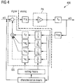
- Figure 4 shows a schematic block diagram of a structure of a hybrid recursive active filter with multi-feedback digital signal processing according to exemplifying embodiments of the present invention. Like in Figures 2 and 3 , four digital feedback paths are illustrated as a non-limiting example, one of which is indicated as a general branch denoted with i.
- the present hybrid recursive active filter (400) comprises setting means and open-loop characterization means.
- the setting means is for setting parameters of the digital signal processing means (i.e. "digital parameters"), including the path-specific attenuation and/or the path-specific delay of one or more of the plurality of digital feedback paths (as indicated by dashed arrows).
- the open-loop characterization means is configured for detecting current open-loop characteristics of the filter, and the setting means is configured to set the parameters of the digital signal processing means on the basis of the thus detected current open-loop characteristics of the filter.
- any parameters of the digital signal processing means can be appropriately set, such as e.g. one or more of 1 / b i , ⁇ di or ⁇ di *, and K.
- the open-loop characteristics of the filter comprise an open-loop gain or, more specifically, an open-loop transfer function for the power amplifier means, analog-to-digital conversion circuitry and digital-to-analog conversion circuitry in the filter.
- the open-loop characterization means is configured to inject, as a calibration input signal, a pilot tone at a modulation carrier position of the output signal (at the input side of the forward path), to measure an open-loop gain for the injected pilot tone (at the input side of the digital signal processing means), and to determine the open-loop characteristics of the filter on the basis of the measured open-loop gain for the injected pilot tone. That is to say, the pilot tone is hidden in the actual signal.
- a pilot signal can be injected at the carrier position (i.e. in the middle of the OFDM signal) in order to measure the gain variations of the analog components and to correct them, choosing a safe point of operation with a high selectivity gain
- the open-loop transfer function can be obtained at the frequency of the pilot tone. Further, the characterization can be obtained as near as possible to the edge of stability of the filter operation (i.e. a point where good selectivity and steepness of the bandpass filter can be reached).
- Figure 5 shows a schematic block diagram of a structure of a hybrid recursive active filter with multi-feedback digital signal processing according to exemplifying embodiments of the present invention.
- the structure of the present hybrid recursive active filter (500) is similar to that of the hybrid recursive active filter of Figure 4 (with four digital feedback paths being illustrated as a non-limiting example, one of which is indicated as a general branch denoted with i). Accordingly, the description of similar points is omitted, while reference is made to the above description of Figure 4 .
- the present structure basically differs in the function of the open-loop characterization means.
- the open-loop characterization means is configured to capture an inbound digital signal after analog-to-digital conversion at the input side of the digital signal processing means, to capture an outbound digital signal before digital-to-analog conversion at the output side of the digital signal processing means, to compare the captured inbound digital signal with the captured outbound digital signal, and to determine the open-loop characteristics of the filter on the basis of the comparison.
- the open-loop transfer function can be obtained as the spectrum at the ADC output divided by the spectrum at the DAC input.
- the open-loop transfer function can be obtained over a wide bandwidth (in contrast to the above pilot tone approach, where the characterization can be obtained at the single frequency of the pilot tone only).
- Both of the open-loop characterization means of Figures 4 and 5 enable a real-time characterization of the open-loop behavior of the filter.
- analog drift and/or fluctuation effects of the analog elements of the filter i.e. the power amplifier means, analog-to-digital conversion circuitry and digital-to-analog conversion circuitry in the filter, can be observed in real-time. Thereby, performance and selectivity can be improved.
- Such characterization can be accomplished during the actual operation of the filter, e.g. the base station comprising the filter, without (remarkably) affecting its operation. That is to say, the open-loop behavior of the filter can be characterized in-situ, i.e. during regular operation, without having to stop an actual operation. Thereby, such characterization can be performed and considered regularly or even (quasi) permanently, thus improving the operability of the filter, without requiring an out-of-service time or a specific (calibration/measurement) mode switching. Moreover, the characterization can be obtained in an actual/large signal regime rather than a small signal regime which would be case in a specific measurement or calibration mode.
- Figures 4 and 5 show respective implementations comprising both setting means and open-loop characterization means for illustrative purposes only, it is also feasible that a hybrid recursive active filter with multi-feedback digital signal processing comprises only the setting means. Thereby, a manual setting of parameters of the digital signal processing means can be enabled. Also, it is to be noted that any one of the setting means and the open-loop characterization means can be realized in an apparatus such as a communication apparatus comprising the filter, but do not need to be realized in the filter as such, as long as the can accomplish the above-described functions, respectively.
- instability can be avoided in that chaotic oscillations massive disturbances, etc. occurring in the instability region can be compensated for.
- the filter of any one of Figure 4 and 5 may be operated in/with a (operating) method comprising setting parameters of the digital signal processing means, also comprising detecting current open-loop characteristics of the filter, wherein the parameters of the digital signal processing means are set on the basis of the detected current open-loop characteristics of the filter.
- the (operating) method may comprise injecting, as a calibration input signal, a pilot tone at a modulation carrier position of the output signal, measuring an open-loop gain for the injected pilot tone, and determining the open-loop characteristics of the filter on the basis of the measured open-loop gain for the injected pilot tone.
- the (operating) method may comprise capturing an inbound digital signal after analog-to-digital conversion at the input side of the digital signal processing means, capturing an outbound digital signal before digital-to-analog conversion at the output side of the digital signal processing means, comparing the captured inbound digital signal with the captured outbound digital signal, and determining the open-loop characteristics of the filter on the basis of the comparison.
- Figure 6 shows a schematic block diagram of a FPGA implementation example of a hybrid recursive active filter with multi-feedback digital signal processing.
- the present hybrid recursive active filter (600) comprises a digital signal processing means in FPGA implementation.
- a High Speed Mezzanine Card (HSMC) is used as an adapter interface between ADC and DAC circuits and the FPGA (motherboard), while this is only an illustrative example.
- HSMC High Speed Mezzanine Card
- the output signal produced by the PA may have around 50 dBm power. It is collected with a coupler an attenuated by 35 dB. Thus, the signal having 15 dBm power is sampled, e.g. by a 12-bit 3.6 GSample/s A/D converter and is fed to the FPGA for digital signal processing. The signal is reconstructed with a fast 16-bit D/A converter running up to 1.5 GSample/s and an I/Q modulator to reach the RF frequency at a power of 0 dBm.
- Figure 6 exemplifies a hybrid recursive active filter in a FPGA implementation for illustrative purposes only, any other implementation of the digital signal processing means is feasible for a hybrid recursive active filter.
- the digital signal processing means can be implemented as an ASIC, a DSP, or the like.
- the filter of any one of Figure 2 to 6 can be included in a radio-frequency unit such as a RF front-end. Further, the filter of any one of Figure 2 to 6 and/or such radio-frequency unit can be included in a communication apparatus.
- a communication apparatus may be compliant with any mobile communication system/standard, such as e.g. GSM, LTE, LTE-A and WCDMA).
- GSM Global System for Mobile communications
- LTE Long Term Evolution
- LTE-A Long Term Evolution-Advance
- WCDMA Wideband Code Division Multiple Access
- Such communication apparatus may be a base station, a base transceiver station, an access node, or the like.
- Figure 7 shows a graph of magnitudes of overall transfer functions for a comparison of a hybrid recursive active filter with multi-feedback digital signal processing, with 20 digital feedback paths (and 1.55 ⁇ s total loop delay), and a hybrid recursive active filter with single-feedback digital signal processing.
- a hybrid recursive active filter with multi-feedback digital signal processing with 20 digital feedback paths (and 1.55 ⁇ s total loop delay)
- a hybrid recursive active filter with single-feedback digital signal processing For the single-feedback case, there are depicted both simulation and measurement results in order to show the reliability of the simulation.
- the curve denoted by 1 represents a normal PA gain (as a normalized result of measurement), i.e. a PA gain without a recursive filter structure
- the curve denoted by 2 represents a gain of a recursive filter (by way of measurement), i.e. a single-feedback filter structure
- the (dashed) curve denoted by 3 represents a gain of a recursive multi-feedback filter structure.
- a passband filter with flat passband gain and not just repetitive narrowband peaks can be obtained, and very high steepness/slope and attenuation over frequency can be attained. Namely, a broader passband can be achieved.
- the passband can be enlarged to about 460 kHz (as compared with about 56 kHz with a single-feedback structure).
- the multi-feedback structure can attain more than eight times - 3dB bandwidth of a single-feedback structure with the same selectivity (20 dB in this case).
- an increased steepness/slope (defined as the ratio of attenuation in dB over frequency, where the attenuation is measured between the cut-off point and the middle point between maximum gain and attenuation of the passband behavior) can be achieved.
- the steepness/slope of the transition bandwidth is 175.75 dB/MHz in the single-feedback case, while the multi-feedback case allows an enhancement of this steepness/slope up to 233 dB/MHz.
- a wide dynamic range can be achieved. In the illustrated example, a dynamic range and selectivity of about 20 dB (between maximum gain and minimum attenuation to the normal output) can be realized.
- a (more) appropriate and flexible shaping can be achieved with a suitable number of digital feedback paths (e.g. even more than 20 digital feedback paths).
- a suitable number of digital feedback paths e.g. even more than 20 digital feedback paths.
- a filter with less overall (group) delay e.g. less than 1.55 ⁇ s, as mentioned above
- the curve denoted by 1 represents simulation results for a hybrid active recursive filter having a multi-feedback filter structure (with 10 digital feedback paths), while the curve denoted by 2 represents simulation results for a conventional hybrid active recursive filter, i.e. a single-feedback filter structure.
- Figures 8 , 10 , 12 , 14 , 16 , 18 and 20 show graphs of a magnitude of the overall transfer function, the phase of the overall transfer function, and the (group) delay of the filter (or transmitter, if implemented in a RF front-end).
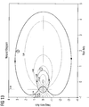
- Figures 9 , 11 , 13 , 15 , 17 , 19 and 21 represent Nyquist diagrams in order to look at the stability of the respective filter configurations.
- hybrid recursive active filters with a digital feedback loop are subject to stability problems.
- a stability analysis is expedient for a full understanding of the behavior and limits of possible instability regions in recursive structures so as to ensure feasibility.
- the real part of the transfer function is plotted on the horizontal axis, and the imaginary part of the transfer function is plotted on the vertical axis, while the frequency is swept as a parameter, resulting in one plot (point) per frequency.
- the Nyquist criterion states that the number of unstable closed-loop poles of the open-loop transfer function is equal to the number of unstable open-loop poles of the open-loop transfer function minus the number of encirclements of the point (-1, j0) (counted positively for a counterclockwise encirclement and negatively for a clockwise encirclement) of the Nyquist plot of the open-loop transfer function.
- the number of unstable closed-loop poles has to be zero, i.e. there must be no positive roots.
- the multi-feedback filter structure enables to adaptively control the passband (e.g. in terms of breadth) and the steepness of the filter.
- the steepness may reach about 17.4 dB attenuation over 100 kHz (as the difference in dB between maximum gain and minimum attenuation over frequency).
- the multi-feedback construction allows an enhancement of the performance of the single-feedback construction, e.g. in terms of steepness/slope and passband width.
- This enhancement is dependent on the number of branches i used for the multi-feedback design and also on the parameter K that controls the distance of the working point from the stability limit.
- multi-feedback construction allows to reject noise added by the analog power amplifier due the hybrid negative (multi-path) feedback.
- the noise introduced by the components in the forward path mainly by the analog power amplifier
- Such reduction may be represented by a division of the forward-path noise by the feedback-path gain/attenuation (in the absolute domain) or subtraction of the feedback-path gain/attenuation from the forward-path noise (in the dB domain).
- the closed-loop system can be controlled so as to obtain the best possible performance.
- the stability is affected just by the gain in the forward path and the attenuation in the feedback loop (i.e. the attenuation in the individual feedback paths) and not by various delays in the system.
- Figure 22 shows a schematic block diagram of a structure of a hybrid recursive active filter with multi-feedback digital signal processing and multi-feedforward digital signal processing according to exemplifying embodiments of the present invention.
- the present hybrid recursive active filter (700) comprises analog power amplifier means (PA) in a forward path for amplifying an input signal to generate an output signal (y(t)) and digital signaling processing means (DS-FB) in a feedback loop for applying a feedback signal on the basis of the output signal (i.e. digital baseband feedback) on the input signal, like in any one of Figures 2 to 5 . That is, the principles of any one of Figures 2 to 5 are equally applicable for the present hybrid recursive active filter (700) as well, and thus reference is made to the description thereof for details in this regard.
- PA analog power amplifier means
- DS-FB digital signaling processing means
- the present hybrid recursive active filter (700) comprises a digital signaling processing means (DS-FF) in a feedforward loop for applying a feedforward signal on the basis of the input signal (i.e. digital baseband feedforward control) on the input signal.
- DS-FF digital signaling processing means
- hybrid negative (multi-path) feedforward control is additionally established in the recursive active filter.
- each digital feedback path is configured to process the input signal with a path-specific attenuation (1 / b, 1 / b 2 , 1 / b 3 , 1 / b 1 ) and a path-specific delay ( ⁇ d , ⁇ d2 , ⁇ d3 , ⁇ di ), and combining means for combining processed signals from the four digital feedforward paths (by way of addition) to generate the feedforward signal. Then, the feedforward signal is mixed with the feedback signal from the digital signaling processing means (DS-FB) in the feedback path (by way of subtraction).
- DS-FB digital signaling processing means
- Figure 22 exemplifies a hybrid recursive active filter with four digital feedforward paths for illustrative purposes only, any number of digital feedforward paths, i.e. one, two or more digital feedforward paths, is feasible in a hybrid recursive active filter according to exemplifying embodiments of the present invention.
- a general branch denoted with i in Figure 22 the thus depicted concept can be applied with an arbitrary number of digital feedforward paths, and is thus to be understood with a general meaning in the broadest sense.
- Figure 22 exemplifies a hybrid recursive active filter in which the configuration of the multi-feedforward loop corresponds to the configuration of the multi-feedback loop (in terms of the number of branches, as well as the denominations (and values) of attenuation and delay elements), this is only an illustration without limiting generality.
- the feedforward loop can be configured independent from the configuration of the feedback loop (in terms of the number of branches, as well as the denominations (and values) of attenuation and delay elements).
- each feedforward path ( 1 / b , 1 / b 2 , 1 / b 3 , 1 / b i ) and/or the path-specific attenuation in each feedforward path ( ⁇ d , ⁇ d2 , ⁇ d3 , ⁇ di ) can be realized and set, as described above for the multi-feedback loop in Figures 2 and 3 , and can optionally be controlled, as described above for Figures 4 and 5 .
- the DS-FF element can also be realized as/in a FPGA-based implementation (in the same or a separate FPGA unit as the DS-FF element), as illustrated in Figure 6 .
- each feedforward path represents an illustrative example only, while the order/sequence thereof may also be reverse, or the attenuation and delay properties may be integrated within a single element
- a hybrid CIC (cascaded-integrator-comb) filter structure can be realized. Accordingly, well-known principles of CIC filters can be directly applied to the hybrid recursive active filter and a radio-frequency unit or transmitter including the same.
- Figure 23 shows graphs of simulation results for a comparison of a hybrid recursive active filter with multi-feedback digital signal processing and feedforward digital signal processing and a hybrid recursive active filter with multi-feedback digital signal processing and without feedforward digital signal processing.
- the curve denoted by 1 represents simulation results for a hybrid active recursive filter with 20 feedback paths and 1 feedforward path (as an example of a hybrid CIC filter structure according to Figure 22 ), and 2 represents simulation results for a hybrid recursive active with 20 feedback paths and 0 feedforward paths (as an example of a filter structure according to any one of Figures 2 to 5 ).
- the transfer function of the hybrid CIC filter structure according to Figure 22 enlarges the suppression bandwidth, i.e. the stopband. Accordingly, such filter structure enables to control the stopband behavior of the recursive active filter (by the digital (multi-) feedforward loop) in addition to the passband behavior of the recursive active filter (which is controlled by the digital (multi-) feedback loop, as explained above).
- a technique for hybrid recursive active filtering with adaptability ensuring appropriate transfer function shaping in view of the aforementioned requirements as well as stable operability, can be enabled/realized. More specifically, frequency-agile and re-/configurable filtering can be attained by way of multiple digital feedback paths. As the parameters of the digital feedback loop can be easily and adaptively set, a software-defined/definable filter can be implemented, thus providing applicability for software-defined/definable or cognitive radio. In the end, a "software defined analogue filter" can be created, which matches the wish for reconfigurability with highly selective analog filters.
- an analog power amplifier or, more generally speaking, an analog transmitter
- an analog power amplifier like an IIR filter
- it is effective in terms of implementation efforts in SDR architectures.
- a bandpass behavior (with a broader passband and/or a broader stopband) of the transmitted signal at the output of the amplifier is obtained, allowing relaxation of duplexer/cavity filter requirements like edge steepness and isolation, saving cost and size of RF front-ends.
- a hybrid recursive active filter with multi-feedback makes available, at the output of the filter/transmitter, a desired bandpass behavior, thus omitting the need for expensive duplex/cavity filters placed after the filter/transmitter and before antennas and the receiver, saving size and costs.
- This can be implemented with common digital hardware already in use e.g. for digital predistortion in common BTS transmitters, and it is frequency agile allowing possible reconfiguration depending on the used communication standard.
- respective functionalities, functional blocks or elements described above can be implemented by any known means, either in hardware and/or software, respectively, if it is only adapted to perform the described functions of the respective parts.
- the mentioned method steps can be realized in individual functional blocks or by individual devices, or one or more of the method steps can be realized in a single functional block or by a single device.
- any structural means such as a portion or other circuitry of an amplifier may refer to one or more of the following: (a) hardware-only circuit implementations (such as implementations in only analog and/or digital circuitry) and (b) combinations of circuits and software (and/or firmware), such as (as applicable): (i) a combination of processor(s) or (ii) portions of processor(s)/software (including digital signal processor(s)), software, and memory(ies) that work together to cause an apparatus, such as a mobile phone or server, to perform various functions) and (c) circuits, such as a microprocessor(s) or a portion of a microprocessor(s), that require software or firmware for operation, even if the software or firmware is not physically present. Also, it may also cover an implementation of merely a processor (or multiple processors) or portion of a processor and its (or their) accompanying software and/or firmware, any integrated circuit, or the like.
- any procedural step or functionality is suitable to be implemented as software/firmware or by hardware without changing the idea of the present invention.
- Such software may be software code independent and can be specified using any known or future developed programming language, such as e.g. Java, C++, C, and Assembler, as long as the functionality defined by the method steps is preserved.
- Such hardware may be hardware type independent and can be implemented using any known or future developed hardware technology or any hybrids of these, such as MOS (Metal Oxide Semiconductor), CMOS (Complementary MOS), BiMOS (Bipolar MOS), BiCMOS (Bipolar CMOS), ECL (Emitter Coupled Logic), TTL (Transistor-Transistor Logic), etc., using for example ASIC (Application Specific IC (Integrated Circuit)) components, FPGA (Field-programmable Gate Arrays) components, CPLD (Complex Programmable Logic Device) components or DSP (Digital Signal Processor) components.
- MOS Metal Oxide Semiconductor
- CMOS Complementary MOS
- BiMOS Bipolar MOS
- BiCMOS BiCMOS
- ECL Emitter Coupled Logic
- TTL Transistor-Transistor Logic
- ASIC Application Specific IC
- FPGA Field-programmable Gate Arrays
- CPLD Complex Programmable Logic Device
- DSP
- a device/apparatus may be represented by a semiconductor chip, a chipset, or a (hardware) module comprising such chip or chipset; this, however, does not exclude the possibility that a functionality of a device/apparatus or module, instead of being hardware implemented, be implemented as software in a (software) module such as a computer program or a computer program product comprising executable software code portions for execution/being run on a processor.
- a device may be regarded as a device/apparatus or as an assembly of more than one device/apparatus, whether functionally in cooperation with each other or functionally independently of each other but in a same device housing, for example.
- Software in the sense of the present description comprises software code as such comprising code means or portions or a computer program or a computer program product for performing the respective functions, as well as software (or a computer program or a computer program product) embodied on a tangible medium such as a computer-readable (storage) medium having stored thereon a respective data structure or code means/portions or embodied in a signal or in a chip, potentially during processing thereof.
- Apparatuses and/or means or parts thereof can be implemented as individual devices, but this does not exclude that they may be implemented in a distributed fashion throughout the system, as long as the functionality of the device is preserved. Such and similar principles are to be considered as known to a skilled person.
- the present invention also covers any conceivable combination of method steps and operations described above, and any conceivable combination of nodes, apparatuses, modules or elements described above, as long as the above-described concepts of methodology and structural arrangement are applicable.
- Such technique exemplarily comprise a hybrid recursive active filter, comprising analog power amplifier means in a forward path for amplifying an input signal to generate an output signal, and digital signaling processing means in a feedback loop for applying a feedback signal on the basis of the output signal on the input signal, wherein the digital signaling processing means comprises a plurality of digital feedback paths, each digital feedback path being configured to process the output signal with a path-specific attenuation and a path-specific delay, and combining means for combining processed signals from the plurality of digital feedback paths to generate the feedback signal.
Description
- The present invention relates to hybrid recursive active filtering with adaptive transfer function shaping capability. More specifically, the present invention relates to a hybrid recursive active filter, a method of operating the same, and a computer program product for carrying out the method of operating the same.
- In order to comply with recent mobile communication standards (such as e.g. GSM, LTE, LTE-A and WCDMA), radio-frequency units like RF front-ends of communication apparatuses (such as e.g. base stations, base transceiver stations, and access nodes) do have to fulfill stringent requirements. Among others, such requirements relate to specifications in terms of out-of-band noise, spurious emissions and wideband noise as well as interference between the transmit and receive bands.
- To this end, duplex filters are used in the RF front-end of a communication apparatus, which are often designed as high-order air cavity band-pass filters having a high quality factor. However, such cavity filters are expensive and have big dimensions, and moreover they are designed to work at an accurately tuned and fixed frequency band only.
- Accordingly, it is desirable to replace such cavity filters with more compact and cost-effective solutions, which are preferably also frequency-adaptive.
- Hybrid recursive active filters are representing a solution to the aforementioned problem. Such filters comprise an analog power amplifier in a forward path and digital signal processing means in a feedback loop. So, analog parts of conventional filters are replaced by digital signal processing means using functional (software-based) algorithms. Thereby, they allow an appropriate quality factor. The article by G. Gottardo et al. "Novel Hybrid Recursive Active Filters in RF Transmitter Front-Ends" published during the 2014 German Microwave Conference (GeMIC) in March 2014 describes such a known filter. Moreover, patent documents
US2001005402 andUS2012314736 and the article by A. P. Lisitskiy et al. "Digital Feedback Parameter Optimization" published in Telecommunications and Radio Engineering, vol. 41/42, no. 8, in August 1987, disclose a power amplifier with a feedback loop including a digital signal processing unit to apply a predistortion to the input of the power amplifier and thus compensate for its non-linearity. - However, while being somewhat frequency-adaptive, known hybrid recursive active filters cannot provide for sufficient adaptability for ensuring appropriate transfer function shaping in view of the aforementioned requirements. Further, due to the digital feedback loop, such hybrid recursive active filters are subject to stability problems.
- Accordingly, there is still a demand for a technique for hybrid recursive active filtering with adaptability, ensuring appropriate transfer function shaping in view of the aforementioned requirements as well as stable operability.
- Various exemplifying embodiments of the present invention aim at addressing at least part of the above issues and/or problems and drawbacks.
- Various aspects of exemplifying embodiments of the present invention are set out in the appended claims.
- According to an example aspect of the present invention, there is provided a hybrid recursive active filter, comprising analog power amplifier means in a forward path for amplifying an amplifier input signal to generate an output signal, and first digital signal processing means in a feedback loop for generating a feedback signal on the basis of the output signal and for combining the feedback signal with the input signal to generate the amplifier input signal, wherein the first digital signal processing means in the feedback loop comprises a plurality of digital feedback paths, each digital feedback path being configured to process the output signal with a path-specific attenuation and a path-specific delay, and combining means for combining processed signals from the plurality of digital feedback paths to generate the feedback signal, setting means for setting parameters of the first digital signal processing means, the parameters including the path-specific attenuation and/or the path-specific delay of one or more of the plurality of digital feedback paths, open-loop characterization means for detecting current open-loop characteristics of the filter, wherein the setting means is configured to set the parameters of the first digital signal processing means on the basis of the detected current open-loop characteristics of the filter, an analog-to-digital conversion circuitry at the input side of the first digital signal processing means, and a digital-to-analog conversion circuitry at the output side of the first digital signal processing means, wherein the open-loop characteristics of the filter comprise an open-loop transfer function for analog elements of the filter, the analog elements including the power amplifier means, the analog-to-digital conversion circuitry and the digital-to-analog conversion circuitry.
- According to an example aspect of the present invention, there is provided a communication apparatus, comprising a radio-frequency unit comprising a hybrid recursive active filter according to the aforementioned example aspect of the present invention.
- According to an example aspect of the present invention, there is provided a method of operating a hybrid recursive active filter, comprising analog power amplifier means in a forward path and first digital signal processing means in a feedback loop, the method comprising amplifying an amplifier input signal by the analog power amplifier means in the forward path to generate an output signal, generating a feedback signal on the basis of the output signal and combining the feedback signal with the input signal to generate the amplifier input signal by the first digital signal processing means in the feedback loop, wherein the feedback signal is generated in the first digital signal processing means by processing the output signal in a plurality of digital feedback paths, each digital feedback path exhibiting a path-specific attenuation and a path-specific delay, and combining processed signals from the plurality of digital feedback paths, setting parameters of the first digital signal processing means, the parameters including the path-specific attenuation and/or the path-specific delay of one or more of the plurality of digital feedback paths, and detecting current open-loop characteristics of the filter, wherein the parameters of the first digital signal processing means are set on the basis of the detected current open-loop characteristics of the filter, and wherein the open-loop characteristics of the filter comprise an open-loop transfer function for analog elements of the filter, the analog elements including the power amplifier means, analog-to-digital conversion circuitry in the filter and digital-to-analog conversion circuitry in the filter.
- According to an example aspect of the present invention, there is provided a computer program product comprising computer-executable computer program code which, when the program code is executed (or run) on a computer or the program is run on a computer (e.g. a computer of an apparatus according to any one of the aforementioned apparatus-related example aspects of the present invention), is configured to cause the computer to carry out the method according to the aforementioned method-related example aspect of the present invention.
- The computer program product may comprise or may be embodied as a (tangible/non-transitory) computer-readable (storage) medium or the like, on which the computer-executable computer program code is stored, and/or the program is directly loadable into an internal memory of the computer or a processor thereof.
- Further developments and/or modifications of the aforementioned example aspects of the present invention are set out in the following.
- By way of exemplifying embodiments of the present invention, a technique for hybrid recursive active filtering with adaptability, ensuring appropriate transfer function shaping in view of the aforementioned requirements as well as stable operability, can be enabled/realized.
- In the following, the present invention will be described in greater detail by way of non-limiting examples with reference to the accompanying drawings, in which
-
Figure 1 shows a schematic block diagram of a structure of a hybrid recursive active filter with single-feedback digital signal processing according to an example for explaining the present invention, -
Figure 2 shows a schematic block diagram of a structure of a hybrid recursive active filter with multi-feedback digital signal processing according to an example for explaining the present invention, -
Figure 3 shows a schematic block diagram of a structure of a hybrid recursive active filter with multi-feedback digital signal processing according to an example for explaining the present invention, -
Figure 4 shows a schematic block diagram of a structure of a hybrid recursive active filter with multi-feedback digital signal processing according to exemplifying embodiments of the present invention, -
Figure 5 shows a schematic block diagram of a structure of a hybrid recursive active filter with multi-feedback digital signal processing according to exemplifying embodiments of the present invention, -
Figure 6 shows a schematic block diagram of a FPGA implementation example of a hybrid recursive active filter with multi-feedback digital signal processing according to an example for explaining the present invention,Figure 7 shows a graph of magnitudes of overall transfer functions for a comparison of a hybrid recursive active filter with multi-feedback digital signal processing, with 20 digital feedback paths and total loop delay 1.55 µs, and a hybrid recursive active filter with single-feedback digital signal processing, -
Figures 8 and9 show graphs of simulation results for a comparison of a hybrid recursive active filter with multi-feedback digital signal processing, with 10 digital feedback paths, total loop delay 1.7 µs and K=-0.8, and a hybrid recursive active filter with single-feedback digital signal processing, -
Figures 10 and11 show graphs of simulation results for a comparison of a hybrid recursive active filter with multi-feedback digital signal processing, with 10 digital feedback paths, total loop delay 1.7 µs and K=0, and a hybrid recursive active filter with single-feedback digital signal processing, -
Figures 12 and13 show graphs of simulation results for a comparison of a hybrid recursive active filter with multi-feedback digital signal processing, with 10 digital feedback paths, total loop delay 1.7 µs and K=-1, and a hybrid recursive active filter with single-feedback digital signal processing, -
Figures 14 and15 show graphs of simulation results for a comparison of a hybrid recursive active filter with multi-feedback digital signal processing, with 10 digital feedback paths, total loop delay 1.7 µs and K=-2, and a hybrid recursive active filter with single-feedback digital signal processing, -
Figures 16 and17 show graphs of simulation results for a comparison of a hybrid recursive active filter with multi-feedback digital signal processing, with 10 digital feedback paths, total loop delay 1.7 µs and K=-3, and a hybrid recursive active filter with single-feedback digital signal processing, -
Figures 18 and19 show graphs of simulation results for a comparison of a hybrid recursive active filter with multi-feedback digital signal processing, with 10 digital feedback paths, total loop delay 1.7 µs and K=-5, and a hybrid recursive active filter with single-feedback digital signal processing, -
Figures 20 and21 show graphs of simulation results for a comparison of a hybrid recursive active filter with multi-feedback digital signal processing, with 10 digital feedback paths, total loop delay 1.7 µs and K=9, and a hybrid recursive active filter with single-feedback digital signal processing, -
Figure 22 shows a schematic block diagram of a structure of a hybrid recursive active filter with multi-feedback digital signal processing and multi-feedforward digital signal processing according to exemplifying embodiments of the present invention, and -
Figure 23 shows graphs of simulation results for a comparison of a hybrid recursive active filter with multi-feedback digital signal processing and feedforward digital signal processing and a hybrid recursive active filter with multi-feedback digital signal processing and without feedforward digital signal processing. - The present invention is described herein with reference to particular non-limiting examples and to what are presently considered to be conceivable embodiments of the present invention. A person skilled in the art will appreciate that the present invention is by no means limited to these examples and embodiments, and may be more broadly applied.
- It is to be noted that the following description of the present invention and its embodiments mainly refers to explanations being used as non-limiting examples for exemplifying purposes. As such, the description of exemplifying embodiments given herein specifically refers to terminology which is related thereto. Such terminology is only used in the context of the presented non-limiting examples, and does naturally not limit the present invention in any way. Rather, any other structures, elements, modules, functionalities, etc. may also be utilized as long as complying with what is described herein and/or exemplifying embodiments described herein are applicable to it.
- Hereinafter, various exemplifying embodiments and implementations of the present invention and its aspects are described using several variants and/or alternatives. It is generally noted that, according to certain needs and constraints, all of the described variants and/or alternatives may be provided alone or in any conceivable combination (also including combinations of individual features of the various variants and/or alternatives). In this description, the words "comprising" and "including" should be understood as not limiting the described exemplifying embodiments and implementations to consist of only those features that have been mentioned, and such exemplifying embodiments and implementations may also contain features, structures, elements, modules, functionalities etc. that have not been specifically mentioned.
- In the drawings, it is noted that lines/arrows interconnecting individual blocks or entities are generally meant to illustrate an operational coupling there-between, which may be a physical and/or logical coupling, which on the one hand is implementation-independent (e.g. wired or wireless) and on the other hand may also comprise an arbitrary number of intermediary functional blocks or entities not shown.
- According to exemplifying embodiments of the present invention, in general terms, there is provided a technique for hybrid recursive active filtering with adaptability, ensuring appropriate transfer function shaping in view of the aforementioned requirements as well as stable operability.
-
Figure 1 shows a schematic block diagram of a structure of a hybrid recursive active filter with single-feedback digital signal processing according to an example for explaining the present invention. - As shown in
Figure 1 , the present hybrid recursive active filter (100) comprises analog power amplifier means (PA) in a forward path for amplifying an input signal (x(t)) to generate an output signal (y(t)) and digital signaling processing means (DS) in a feedback loop for applying a feedback signal on the basis of the output signal (i.e. digital baseband feedback) on the input signal. In the digital signaling processing means (DS), the output signal is processed by a single feedback path exhibiting a path-specific attenuation (1/b) and a path-specific delay (τd), and the processed signal is mixed with the input signal (by way of subtraction). Further, a represents a gain introduced the forward path by the power amplifier means, τTX represents a delay introduced in the forward path by analog circuitry (such as DAC circuitry (not shown) at the boundary between the digital and the analog domains), τa represents a delay introduced in the forward path by the power amplifier means, and τRX represents a delay introduced in the feedback loop by analog circuitry (such as ADC circuitry (not shown) at the boundary between the analog and the digital domains). -
Figure 2 shows a schematic block diagram of a structure of a hybrid recursive active filter with multi-feedback digital signal processing according to an example for explaining the present invention. As shown inFigure 2 , the present hybrid recursive active filter (200) comprises analog power amplifier means (PA) in a forward path for amplifying an input signal (x(t)) to generate an output signal (y(t)) and digital signaling processing means (DS) in a feedback loop for applying a feedback signal on the basis of the output signal (i.e. digital baseband feedback) on the input signal. In the digital signaling processing means (DS), as a non-limiting example, there are four digital feedback paths for processing the output signal, respectively. Each digital feedback path is configured to process the output signal with a path-specific attenuation (1/b, 1/b2, 1/b3, 1/bi) and a path-specific delay (τd, τd2, τd3, τdi), and combining means for combining processed signals from the four digital feedback paths (by way of addition) to generate the feedback signal. Then, the feedback signal is mixed with the input signal (by way of subtraction). Further, like inFigure 1 , a represents a gain introduced in the forward path by the power amplifier means, τTX represents a delay introduced in the forward path by analog circuitry (such as DAC circuitry (not shown) at the boundary between the digital and the analog domains), τa represents a delay introduced in the forward path by the power amplifier means, and τRX represents a delay introduced in the feedback loop by analog circuitry (such as ADC circuitry (not shown) at the boundary between the analog and the digital domains). - As evident from
Figure 2 , a multi-feedback digital structure is used to recombine the feedback-digitalized signal with different latencies and attenuations. Thereby, a hybrid negative (multi-path) feedback is established in the recursive active filter. As shown below, an enlarged bandwidth of the pass-band peaks and/or an increased slope/steepness of the transfer function can thus be attained, for example. Using such hybrid solution (i.e. digital feedback applying on an analog power amplifier), a number of real-time adaptive digital designs are possible in order to obtain the desired transfer function over frequency at the filter/transmitter output. - It is to be noted that, while
Figure 2 exemplifies a hybrid recursive active filter with four digital feedback paths for illustrative purposes only, any number of a plurality of digital feedback paths, i.e. two or more digital feedback paths, is feasible in a hybrid recursive active filter with multi-feedback digital signal processing. Namely, as indicated by a general branch denoted with i inFigure 2 , the thus depicted concept can be applied with an arbitrary number of digital feedback paths, and is thus to be understood with a general meaning in the broadest sense. As non-limiting examples thereof, implementations with 10 and 20 branches are discussed below for illustrative purposes only. - Also, it is to be noted that the order/sequence of attenuation and delay elements in each feedback path represents an illustrative example only, while the order/sequence thereof may also be reverse, or the attenuation and delay properties may be integrated within a single element.
- In the filter of
Figure 2 , the path-specific attenuation (1/b) in an i-th feedback path, with i ≥ 2, can be set (as a non-limiting example) by
- As will be evident from the below description and comparison of simulation results (in
Figures 8 to 21 ), K is a parameter that changes the steepness of the transition bandwidth (between the pass band and the stop band regions) and - at the same time - controls the distance of the working point of the filter from the point of instability. The value of parameter K can be changed in order to control the operation of the filter, either manually or automatically e.g. depending on current open-loop characteristics of the filter (as described in connection withFigures 4 and5 below). - As shown in
Figure 2 , the path-specific attenuation in each feedback path can be provided by an attenuation element having a corresponding attenuation. - In the filter of
Figure 2 , the path-specific delay (τd) in an i-th feedback path, with i ≥ 2, can be set (as a non-limiting example) by
- As shown in
Figure 2 , the path-specific delay in each feedback path is provided by a delay element having a corresponding delay. - As a numerical example, the present hybrid recursive active filter (200) can be realized with the following parameters:
- a = 9 dB
- 1/b = - 10.8 dB (including coupler and attenuation)
- 1/b2 = - 10 dB (including coupler and attenuation)
- 1/b3 = - 10.2 dB (including coupler and attenuation)

- ....... (e.g. 1/b19 = - 149.4 dB (including coupler and attenuation))
- τd = 1 clock tick (≅ 0)

- In such design example (upon which the curve denoted by ③ in
Figure 7 is based), a hybrid recursive active filter with a wide dynamic range and selectivity, a broad passband, and an increased steepness/slope can be realized. -
Figure 3 shows a schematic block diagram of a second example structure of a hybrid recursive active filter with multi-feedback digital signal processing according to an example for explaining the present invention. - As shown in
Figure 3 , the structure of the present hybrid recursive active filter (300) is similar to that of the hybrid recursive active filter ofFigure 2 (with four digital feedback paths being illustrated as a non-limiting example, one of which is indicated as a general branch denoted with i). Accordingly, the description of similar points is omitted, while reference is made to the above description ofFigure 2 . The present structure basically differs in the provision of path-specific delay in digital feedback paths with a rank of 2 or more. - In the filter of
Figure 3 , while the path-specific delay (τd) in an i-th feedback path, with i ≥ 2, can be set as indicated above for the filter ofFigure 2 , the path-specific delay in each feedback path is not provided by a delay element having a corresponding delay. Rather, the path-specific delay in each feedback path is provided by the sum of all delay elements in feedback paths with a lower rank and a delay element (in the subject feedback path) having a delay τd* set by
- This is based on the following considerations, as explained below.
- The value of τ is dependent on system technology and/or architecture of the filter, e.g. 1.7 µs. In view of the above equation for the path-specific delay, as described for the filter of
Figure 2 , it holds that:

- The problem of this expression is that the path-specific delay for each feedback path of a rank of 2 or more can only be accurately calculated when the values of the delays τTX, τa and τRX are accurately known. As such knowledge might not be reliably available, it is difficult to properly construct the feedback paths. To avoid this problem, the delays can also be expressed in another way.
- From the initial expression, it can be followed that:

- Moreover, the following holds:


- This means that each feedback path adds just τd every time with respect to the previous feedback path, and it means that the delays of the individual delay elements used in the structure of
Figure 3 can (as a non-limiting example) be:
- So, the delay element in the feedback path with rank 2 (τd2*) has the value τ, and the overall delay in this feedback path is τd + τd2*. Further, the delay element in the feedback path with rank 3 (τd3*) also has the value τ, and the overall delay in this feedback path is τd + τd2* + τd3* , and so forth.
- As compared with the structure of
Figure 2 , the structure ofFigure 3 is beneficial in terms of hardware resource usage, e.g. in a FPGA implementation of the digital signal processing means. Namely, the path-specific delays of all feedback paths can thereby by provided using less delay blocks and resources e.g. of a FPGA. For example, considering the case of τ = 1.7 µs and a sampling frequency of 120 MHz, the structure ofFigure 2 would require a shift register with a total length of 9000 shifts, while the structure ofFigure 2 could get along with a shift register with a total length of about 2100 shifts, i.e. less than 25% compared to the other structure. Further, the calculation of uncertain parameters can be avoided, thus saving processing/computation power. - Although not illustrated herein, it is to be noted that similar considerations and results, as described above for the delay, equally apply for the attenuation as well. In brief, instead of providing the path-specific attenuation in each feedback path by an attenuation element having a corresponding attenuation, the path-specific attenuation in each feedback path by the sum of all attenuation elements in feedback paths with a lower rank and an attenuation element (in the subject feedback path).
- The filter of any one of
Figure 2 and3 may be operated in/with a (operating method) comprising amplifying an input signal by the analog power amplifier means in the forward path to generate an output signal, and applying a feedback signal on the basis of the output signal on the input signal by the digital signaling processing means in the feedback loop, wherein the feedback signal is generated in the digital signaling processing means by processing the output signal in a plurality of digital feedback paths, each digital feedback path exhibiting a path-specific attenuation and a path-specific delay, and combining processed signals from the plurality of digital feedback paths. -
Figure 4 shows a schematic block diagram of a structure of a hybrid recursive active filter with multi-feedback digital signal processing according to exemplifying embodiments of the present invention. Like inFigures 2 and3 , four digital feedback paths are illustrated as a non-limiting example, one of which is indicated as a general branch denoted with i. - As shown in
Figure 4 , the present hybrid recursive active filter (400) comprises setting means and open-loop characterization means. The setting means is for setting parameters of the digital signal processing means (i.e. "digital parameters"), including the path-specific attenuation and/or the path-specific delay of one or more of the plurality of digital feedback paths (as indicated by dashed arrows). The open-loop characterization means is configured for detecting current open-loop characteristics of the filter, and the setting means is configured to set the parameters of the digital signal processing means on the basis of the thus detected current open-loop characteristics of the filter. - Thereby, an automatic setting of parameters of the digital signal processing means (or, stated in other words, a (real-time) configuration or calibration of the filter) can be enabled. Namely, any parameters of the digital signal processing means can be appropriately set, such as e.g. one or more of 1/bi , τdi or τdi*, and K.
- Herein, the open-loop characteristics of the filter comprise an open-loop gain or, more specifically, an open-loop transfer function for the power amplifier means, analog-to-digital conversion circuitry and digital-to-analog conversion circuitry in the filter.
- As indicated in
Figure 4 , the open-loop characterization means is configured to inject, as a calibration input signal, a pilot tone at a modulation carrier position of the output signal (at the input side of the forward path), to measure an open-loop gain for the injected pilot tone (at the input side of the digital signal processing means), and to determine the open-loop characteristics of the filter on the basis of the measured open-loop gain for the injected pilot tone. That is to say, the pilot tone is hidden in the actual signal. For example, in the case of OFDM modulation, a pilot signal can be injected at the carrier position (i.e. in the middle of the OFDM signal) in order to measure the gain variations of the analog components and to correct them, choosing a safe point of operation with a high selectivity gain - By way of such approach, the open-loop transfer function can be obtained at the frequency of the pilot tone. Further, the characterization can be obtained as near as possible to the edge of stability of the filter operation (i.e. a point where good selectivity and steepness of the bandpass filter can be reached).
-
Figure 5 shows a schematic block diagram of a structure of a hybrid recursive active filter with multi-feedback digital signal processing according to exemplifying embodiments of the present invention. - As shown in
Figure 5 , the structure of the present hybrid recursive active filter (500) is similar to that of the hybrid recursive active filter ofFigure 4 (with four digital feedback paths being illustrated as a non-limiting example, one of which is indicated as a general branch denoted with i). Accordingly, the description of similar points is omitted, while reference is made to the above description ofFigure 4 . The present structure basically differs in the function of the open-loop characterization means. - As indicated in
Figure 5 , the open-loop characterization means is configured to capture an inbound digital signal after analog-to-digital conversion at the input side of the digital signal processing means, to capture an outbound digital signal before digital-to-analog conversion at the output side of the digital signal processing means, to compare the captured inbound digital signal with the captured outbound digital signal, and to determine the open-loop characteristics of the filter on the basis of the comparison. - By way of such approach, the open-loop transfer function can be obtained as the spectrum at the ADC output divided by the spectrum at the DAC input. Thus, due to the strict digital nature of the comparison, the open-loop transfer function can be obtained over a wide bandwidth (in contrast to the above pilot tone approach, where the characterization can be obtained at the single frequency of the pilot tone only).
- Both of the open-loop characterization means of
Figures 4 and5 enable a real-time characterization of the open-loop behavior of the filter. By way of such characterization, analog drift and/or fluctuation effects of the analog elements of the filter, i.e. the power amplifier means, analog-to-digital conversion circuitry and digital-to-analog conversion circuitry in the filter, can be observed in real-time. Thereby, performance and selectivity can be improved. - Such characterization can be accomplished during the actual operation of the filter, e.g. the base station comprising the filter, without (remarkably) affecting its operation. That is to say, the open-loop behavior of the filter can be characterized in-situ, i.e. during regular operation, without having to stop an actual operation. Thereby, such characterization can be performed and considered regularly or even (quasi) permanently, thus improving the operability of the filter, without requiring an out-of-service time or a specific (calibration/measurement) mode switching. Moreover, the characterization can be obtained in an actual/large signal regime rather than a small signal regime which would be case in a specific measurement or calibration mode.
- It is to be noted, while
Figures 4 and5 show respective implementations comprising both setting means and open-loop characterization means for illustrative purposes only, it is also feasible that a hybrid recursive active filter with multi-feedback digital signal processing comprises only the setting means. Thereby, a manual setting of parameters of the digital signal processing means can be enabled. Also, it is to be noted that any one of the setting means and the open-loop characterization means can be realized in an apparatus such as a communication apparatus comprising the filter, but do not need to be realized in the filter as such, as long as the can accomplish the above-described functions, respectively. - By way of a corresponding parameter setting in the digital feedback loop (i.e. a corresponding configuration or calibration of the filter), instability can be avoided in that chaotic oscillations massive disturbances, etc. occurring in the instability region can be compensated for.
- It is to be noted that, although not illustrated, the above-described principles of digital parameter setting and/or open-loop characterization are equally applicable to a hybrid recursive active filter with single-feedback digital signal processing, such as that of
Figure 1 . - According to exemplifying embodiments of the present invention, the filter of any one of
Figure 4 and5 may be operated in/with a (operating) method comprising setting parameters of the digital signal processing means, also comprising detecting current open-loop characteristics of the filter, wherein the parameters of the digital signal processing means are set on the basis of the detected current open-loop characteristics of the filter. For open-loop characterization, the (operating) method may comprise injecting, as a calibration input signal, a pilot tone at a modulation carrier position of the output signal, measuring an open-loop gain for the injected pilot tone, and determining the open-loop characteristics of the filter on the basis of the measured open-loop gain for the injected pilot tone. Alternatively, for open-loop characterization, the (operating) method may comprise capturing an inbound digital signal after analog-to-digital conversion at the input side of the digital signal processing means, capturing an outbound digital signal before digital-to-analog conversion at the output side of the digital signal processing means, comparing the captured inbound digital signal with the captured outbound digital signal, and determining the open-loop characteristics of the filter on the basis of the comparison. -
Figure 6 shows a schematic block diagram of a FPGA implementation example of a hybrid recursive active filter with multi-feedback digital signal processing. - As shown in
Figure 6 , the present hybrid recursive active filter (600) comprises a digital signal processing means in FPGA implementation. In the example implementation ofFigure 6 , a High Speed Mezzanine Card (HSMC) is used as an adapter interface between ADC and DAC circuits and the FPGA (motherboard), while this is only an illustrative example. - The output signal produced by the PA may have around 50 dBm power. It is collected with a coupler an attenuated by 35 dB. Thus, the signal having 15 dBm power is sampled, e.g. by a 12-bit 3.6 GSample/s A/D converter and is fed to the FPGA for digital signal processing. The signal is reconstructed with a fast 16-bit D/A converter running up to 1.5 GSample/s and an I/Q modulator to reach the RF frequency at a power of 0 dBm.
- With such high-speed A/D converter, it is possible to avoid the use of a mixer for the analog down conversion in order to decrease the noise figure commonly added in the feedback by analog mixing. Thus, the use of digital down conversion allows to reach frequency agility and a feedback loop with configurable bandwidth.
- It is to be noted that, while
Figure 6 exemplifies a hybrid recursive active filter in a FPGA implementation for illustrative purposes only, any other implementation of the digital signal processing means is feasible for a hybrid recursive active filter. For example, the digital signal processing means can be implemented as an ASIC, a DSP, or the like. - The filter of any one of
Figure 2 to 6 can be included in a radio-frequency unit such as a RF front-end. Further, the filter of any one ofFigure 2 to 6 and/or such radio-frequency unit can be included in a communication apparatus. Such communication apparatus may be compliant with any mobile communication system/standard, such as e.g. GSM, LTE, LTE-A and WCDMA). For example, such communication apparatus may be a base station, a base transceiver station, an access node, or the like. - In the following, performance of various types/implementations is briefly discussed with reference to various graphs.
- Firstly, an example with real parameters for multi-feedback is presented, together with the difference between single- and multi-feedback configurations.
-
Figure 7 shows a graph of magnitudes of overall transfer functions for a comparison of a hybrid recursive active filter with multi-feedback digital signal processing, with 20 digital feedback paths (and 1.55 µs total loop delay), and a hybrid recursive active filter with single-feedback digital signal processing. For the single-feedback case, there are depicted both simulation and measurement results in order to show the reliability of the simulation. - In
Figure 7 , the curve denoted by ① represents a normal PA gain (as a normalized result of measurement), i.e. a PA gain without a recursive filter structure, the curve denoted by ② represents a gain of a recursive filter (by way of measurement), i.e. a single-feedback filter structure, and the (dashed) curve denoted by ③ represents a gain of a recursive multi-feedback filter structure. - As evident from
Figure 7 , the transfer function of a normal PA without a recursive filter structure is nearly constant over bandwidth, while the transfer function of a recursive filter structure describes a periodic bandpass filter response. - By way of provision of a multi-feedback structure, a passband filter with flat passband gain and not just repetitive narrowband peaks can be obtained, and very high steepness/slope and attenuation over frequency can be attained. Namely, a broader passband can be achieved. In the illustrated example (with 9dB forward gain and 10.8 dB attenuation in the feedback and 1.55 µs latency), the passband can be enlarged to about 460 kHz (as compared with about 56 kHz with a single-feedback structure). Hence, the multi-feedback structure can attain more than eight times - 3dB bandwidth of a single-feedback structure with the same selectivity (20 dB in this case). Further, an increased steepness/slope (defined as the ratio of attenuation in dB over frequency, where the attenuation is measured between the cut-off point and the middle point between maximum gain and attenuation of the passband behavior) can be achieved. In the illustrated example, the steepness/slope of the transition bandwidth is 175.75 dB/MHz in the single-feedback case, while the multi-feedback case allows an enhancement of this steepness/slope up to 233 dB/MHz. Still further, a wide dynamic range can be achieved. In the illustrated example, a dynamic range and selectivity of about 20 dB (between maximum gain and minimum attenuation to the normal output) can be realized.
- As mentioned above, a (more) appropriate and flexible shaping can be achieved with a suitable number of digital feedback paths (e.g. even more than 20 digital feedback paths). With a larger number of digital feedback paths, not only the bandwidth of the passband can be enhanced, but also the slope/steepness of the transition band, allowing the design of filters with high quality factors. It is to be noted that a filter with less overall (group) delay (e.g. less than 1.55 µs, as mentioned above) can be used in order to obtain less repetitions over frequency and a larger bandwidth for each resonance peak.
- In all of
Figures 8 to 21 , the curve denoted by ① represents simulation results for a hybrid active recursive filter having a multi-feedback filter structure (with 10 digital feedback paths), while the curve denoted by ② represents simulation results for a conventional hybrid active recursive filter, i.e. a single-feedback filter structure. - The simulations are made for τ = 1.7 µs and a = 0dB, the path-specific delay (τd) in an i-th feedback path, with i ≥ 2, is set by:


- Further, it holds that

- Secondly, it is presented how the transfer function changes with the variation of parameter K.
Figures 8 ,10 ,12 ,14 ,16 ,18 and20 show graphs of a magnitude of the overall transfer function, the phase of the overall transfer function, and the (group) delay of the filter (or transmitter, if implemented in a RF front-end). -
Figures 9 ,11 ,13 ,15 ,17 ,19 and21 represent Nyquist diagrams in order to look at the stability of the respective filter configurations. - Namely, as mentioned above, hybrid recursive active filters with a digital feedback loop are subject to stability problems. Thus, a stability analysis is expedient for a full understanding of the behavior and limits of possible instability regions in recursive structures so as to ensure feasibility. In the Nyquist diagram, in Cartesian coordinates, the real part of the transfer function is plotted on the horizontal axis, and the imaginary part of the transfer function is plotted on the vertical axis, while the frequency is swept as a parameter, resulting in one plot (point) per frequency.
- The Nyquist criterion states that the number of unstable closed-loop poles of the open-loop transfer function is equal to the number of unstable open-loop poles of the open-loop transfer function minus the number of encirclements of the point (-1, j0) (counted positively for a counterclockwise encirclement and negatively for a clockwise encirclement) of the Nyquist plot of the open-loop transfer function. For stability, the number of unstable closed-loop poles has to be zero, i.e. there must be no positive roots.
-
Figures 8 and9 show graphs of simulation results for a comparison of a hybrid recursive active filter with multi-feedback digital signal processing, with 10 digital feedback paths (and 1.7 µs total loop delay) and K=-0.8, and a hybrid recursive active filter with single-feedback digital signal processing, -
Figures 10 and11 show graphs of simulation results for a comparison of a hybrid recursive active filter with multi-feedback digital signal processing, with 10 digital feedback paths (and 1.7 µs total loop delay) and K=0, and a hybrid recursive active filter with single-feedback digital signal processing, -
Figures 12 and13 show graphs of simulation results for a comparison of a hybrid recursive active filter with multi-feedback digital signal processing, with 10 digital feedback paths (and 1.7 µs total loop delay) and K=-1, and a hybrid recursive active filter with single-feedback digital signal processing, -
Figures 14 and15 show graphs of simulation results for a comparison of a hybrid recursive active filter with multi-feedback digital signal processing, with 10 digital feedback paths (and 1.7 µs total loop delay) and K=-2, and a hybrid recursive active filter with single-feedback digital signal processing, -
Figures 16 and17 show graphs of simulation results for a comparison of a hybrid recursive active filter with multi-feedback digital signal processing, with 10 digital feedback paths (and 1.7 µs total loop delay) and K=-3, and a hybrid recursive active filter with single-feedback digital signal processing, -
Figures 18 and19 show graphs of simulation results for a comparison of a hybrid recursive active filter with multi-feedback digital signal processing, with 10 digital feedback paths (and 1.7 µs total loop delay) and K=-5, and a hybrid recursive active filter with single-feedback digital signal processing, and -
Figures 20 and21 show graphs of simulation results for a comparison of a hybrid recursive active filter with multi-feedback digital signal processing, with 10 digital feedback paths (and 1.7 µs total loop delay) and K=9, and a hybrid recursive active filter with single-feedback digital signal processing. - As evident from
Figures 8 to 21 , the multi-feedback filter structure enables to adaptively control the passband (e.g. in terms of breadth) and the steepness of the filter. For example, in the case ofFigure 8 , the steepness may reach about 17.4 dB attenuation over 100 kHz (as the difference in dB between maximum gain and minimum attenuation over frequency). - From the Nyquist diagrams, it can be seen that the parameter K shall be greater than -3 in order to ensure stable operation. Namely, the case of K = -3 represents the theoretical limit (see
Figure 17 ), while the case of K = -5 results in instability (seeFigure 19 ). When K is very big, the multi-feedback structure actually reduces to a single-feedback structure (which is equivalent to the application of a huge attenuation in all feedback paths). This is discernable from the case of K = 9 (seeFigure 21 ). - With the above-described examples, it can be seen how the multi-feedback construction allows an enhancement of the performance of the single-feedback construction, e.g. in terms of steepness/slope and passband width. This enhancement is dependent on the number of branches i used for the multi-feedback design and also on the parameter K that controls the distance of the working point from the stability limit.
- Still further, multi-feedback construction according to (exemplifying embodiments of) the present invention allows to reject noise added by the analog power amplifier due the hybrid negative (multi-path) feedback. It can be shown that the noise introduced by the components in the forward path (mainly by the analog power amplifier) is reduced by an amount corresponding to the gain/attenuation in the (overall) feedback path, i.e. by the hybrid negative (multi-path) feedback. Such reduction may be represented by a division of the forward-path noise by the feedback-path gain/attenuation (in the absolute domain) or subtraction of the feedback-path gain/attenuation from the forward-path noise (in the dB domain).
- By way of such feasibility study of stability, the closed-loop system can be controlled so as to obtain the best possible performance. In this regard, it is to be noted that the stability is affected just by the gain in the forward path and the attenuation in the feedback loop (i.e. the attenuation in the individual feedback paths) and not by various delays in the system.
-
Figure 22 shows a schematic block diagram of a structure of a hybrid recursive active filter with multi-feedback digital signal processing and multi-feedforward digital signal processing according to exemplifying embodiments of the present invention. - As shown in
Figure 22 , the present hybrid recursive active filter (700) comprises analog power amplifier means (PA) in a forward path for amplifying an input signal to generate an output signal (y(t)) and digital signaling processing means (DS-FB) in a feedback loop for applying a feedback signal on the basis of the output signal (i.e. digital baseband feedback) on the input signal, like in any one ofFigures 2 to 5 . That is, the principles of any one ofFigures 2 to 5 are equally applicable for the present hybrid recursive active filter (700) as well, and thus reference is made to the description thereof for details in this regard. - Further, the present hybrid recursive active filter (700) comprises a digital signaling processing means (DS-FF) in a feedforward loop for applying a feedforward signal on the basis of the input signal (i.e. digital baseband feedforward control) on the input signal. Thus, hybrid negative (multi-path) feedforward control is additionally established in the recursive active filter.
- In the digital signaling processing means (DS-FF) in the forward path, as a non-limiting example, there are four digital feedback paths for processing the input signal, respectively. Each digital feedback path is configured to process the input signal with a path-specific attenuation (1/b, 1/b2, 1/b3, 1/b1) and a path-specific delay (τd, τd2, τd3, τdi), and combining means for combining processed signals from the four digital feedforward paths (by way of addition) to generate the feedforward signal. Then, the feedforward signal is mixed with the feedback signal from the digital signaling processing means (DS-FB) in the feedback path (by way of subtraction).
- It is to be noted that, while
Figure 22 exemplifies a hybrid recursive active filter with four digital feedforward paths for illustrative purposes only, any number of digital feedforward paths, i.e. one, two or more digital feedforward paths, is feasible in a hybrid recursive active filter according to exemplifying embodiments of the present invention. For example, as indicated by a general branch denoted with i inFigure 22 , the thus depicted concept can be applied with an arbitrary number of digital feedforward paths, and is thus to be understood with a general meaning in the broadest sense. - Further, it is to be noted that, while
Figure 22 exemplifies a hybrid recursive active filter in which the configuration of the multi-feedforward loop corresponds to the configuration of the multi-feedback loop (in terms of the number of branches, as well as the denominations (and values) of attenuation and delay elements), this is only an illustration without limiting generality. Specifically, it is to be noted that the feedforward loop can be configured independent from the configuration of the feedback loop (in terms of the number of branches, as well as the denominations (and values) of attenuation and delay elements). - Still further, it is to be noted that the path-specific attenuation in each feedforward path (1/b, 1/b2 , 1/b3 , 1/bi ) and/or the path-specific attenuation in each feedforward path (τd, τd2, τd3, τdi) can be realized and set, as described above for the multi-feedback loop in
Figures 2 and3 , and can optionally be controlled, as described above forFigures 4 and5 . Like the DS-FB element, the DS-FF element can also be realized as/in a FPGA-based implementation (in the same or a separate FPGA unit as the DS-FF element), as illustrated inFigure 6 . - As with the feedback loop, it is to be noted that the order/sequence of attenuation and delay elements in each feedforward path represents an illustrative example only, while the order/sequence thereof may also be reverse, or the attenuation and delay properties may be integrated within a single element
- According to exemplifying embodiments of the present invention, as illustrated in
Figure 22 , a hybrid CIC (cascaded-integrator-comb) filter structure can be realized. Accordingly, well-known principles of CIC filters can be directly applied to the hybrid recursive active filter and a radio-frequency unit or transmitter including the same. -
Figure 23 shows graphs of simulation results for a comparison of a hybrid recursive active filter with multi-feedback digital signal processing and feedforward digital signal processing and a hybrid recursive active filter with multi-feedback digital signal processing and without feedforward digital signal processing. - In all of
Figure 23 , the curve denoted by ① represents simulation results for a hybrid active recursive filter with 20 feedback paths and 1 feedforward path (as an example of a hybrid CIC filter structure according toFigure 22 ), and ② represents simulation results for a hybrid recursive active with 20 feedback paths and 0 feedforward paths (as an example of a filter structure according to any one ofFigures 2 to 5 ). - As evident from
Figure 23 , the transfer function of the hybrid CIC filter structure according toFigure 22 enlarges the suppression bandwidth, i.e. the stopband. Accordingly, such filter structure enables to control the stopband behavior of the recursive active filter (by the digital (multi-) feedforward loop) in addition to the passband behavior of the recursive active filter (which is controlled by the digital (multi-) feedback loop, as explained above). - By virtue of exemplifying embodiments of the present invention, as evident from the above, a technique for hybrid recursive active filtering with adaptability, ensuring appropriate transfer function shaping in view of the aforementioned requirements as well as stable operability, can be enabled/realized. More specifically, frequency-agile and re-/configurable filtering can be attained by way of multiple digital feedback paths. As the parameters of the digital feedback loop can be easily and adaptively set, a software-defined/definable filter can be implemented, thus providing applicability for software-defined/definable or cognitive radio. In the end, a "software defined analogue filter" can be created, which matches the wish for reconfigurability with highly selective analog filters.
- The usage of digital feedback acting on an analog power amplifier (or, more generally speaking, an analog transmitter), like an IIR filter, is useful for enabling adaptability, ensuring appropriate transfer function shaping as well as stable operability. Further, it is effective in terms of implementation efforts in SDR architectures. In this regard, a bandpass behavior (with a broader passband and/or a broader stopband) of the transmitted signal at the output of the amplifier is obtained, allowing relaxation of duplexer/cavity filter requirements like edge steepness and isolation, saving cost and size of RF front-ends.
- As explained above, a hybrid recursive active filter with multi-feedback makes available, at the output of the filter/transmitter, a desired bandpass behavior, thus omitting the need for expensive duplex/cavity filters placed after the filter/transmitter and before antennas and the receiver, saving size and costs. This can be implemented with common digital hardware already in use e.g. for digital predistortion in common BTS transmitters, and it is frequency agile allowing possible reconfiguration depending on the used communication standard.
- In general, it is to be noted that respective functionalities, functional blocks or elements described above can be implemented by any known means, either in hardware and/or software, respectively, if it is only adapted to perform the described functions of the respective parts. The mentioned method steps can be realized in individual functional blocks or by individual devices, or one or more of the method steps can be realized in a single functional block or by a single device.
- Generally, any structural means such as a portion or other circuitry of an amplifier may refer to one or more of the following: (a) hardware-only circuit implementations (such as implementations in only analog and/or digital circuitry) and (b) combinations of circuits and software (and/or firmware), such as (as applicable): (i) a combination of processor(s) or (ii) portions of processor(s)/software (including digital signal processor(s)), software, and memory(ies) that work together to cause an apparatus, such as a mobile phone or server, to perform various functions) and (c) circuits, such as a microprocessor(s) or a portion of a microprocessor(s), that require software or firmware for operation, even if the software or firmware is not physically present. Also, it may also cover an implementation of merely a processor (or multiple processors) or portion of a processor and its (or their) accompanying software and/or firmware, any integrated circuit, or the like.
- Generally, any procedural step or functionality is suitable to be implemented as software/firmware or by hardware without changing the idea of the present invention. Such software may be software code independent and can be specified using any known or future developed programming language, such as e.g. Java, C++, C, and Assembler, as long as the functionality defined by the method steps is preserved. Such hardware may be hardware type independent and can be implemented using any known or future developed hardware technology or any hybrids of these, such as MOS (Metal Oxide Semiconductor), CMOS (Complementary MOS), BiMOS (Bipolar MOS), BiCMOS (Bipolar CMOS), ECL (Emitter Coupled Logic), TTL (Transistor-Transistor Logic), etc., using for example ASIC (Application Specific IC (Integrated Circuit)) components, FPGA (Field-programmable Gate Arrays) components, CPLD (Complex Programmable Logic Device) components or DSP (Digital Signal Processor) components. A device/apparatus may be represented by a semiconductor chip, a chipset, or a (hardware) module comprising such chip or chipset; this, however, does not exclude the possibility that a functionality of a device/apparatus or module, instead of being hardware implemented, be implemented as software in a (software) module such as a computer program or a computer program product comprising executable software code portions for execution/being run on a processor. A device may be regarded as a device/apparatus or as an assembly of more than one device/apparatus, whether functionally in cooperation with each other or functionally independently of each other but in a same device housing, for example.
- Software in the sense of the present description comprises software code as such comprising code means or portions or a computer program or a computer program product for performing the respective functions, as well as software (or a computer program or a computer program product) embodied on a tangible medium such as a computer-readable (storage) medium having stored thereon a respective data structure or code means/portions or embodied in a signal or in a chip, potentially during processing thereof.
- Apparatuses and/or means or parts thereof can be implemented as individual devices, but this does not exclude that they may be implemented in a distributed fashion throughout the system, as long as the functionality of the device is preserved. Such and similar principles are to be considered as known to a skilled person.
- The present invention also covers any conceivable combination of method steps and operations described above, and any conceivable combination of nodes, apparatuses, modules or elements described above, as long as the above-described concepts of methodology and structural arrangement are applicable.
- In view of the above, there is provided a technique of hybrid recursive active filtering with adaptive transfer function shaping capability. Such technique exemplarily comprise a hybrid recursive active filter, comprising analog power amplifier means in a forward path for amplifying an input signal to generate an output signal, and digital signaling processing means in a feedback loop for applying a feedback signal on the basis of the output signal on the input signal, wherein the digital signaling processing means comprises a plurality of digital feedback paths, each digital feedback path being configured to process the output signal with a path-specific attenuation and a path-specific delay, and combining means for combining processed signals from the plurality of digital feedback paths to generate the feedback signal.
- Even though the invention is described above with reference to the examples according to the accompanying drawings, it is to be understood that the invention is not restricted thereto. Rather, it is apparent to those skilled in the art that the present invention can be modified in many ways without departing from the scope of the inventive idea as disclosed herein.
-
- ADC
- Analog-to-Digital Converter
- ASIC
- Application-Specific Integrated Circuit
- CIC
- Cascaded-Integrator-Comb
- DAC
- Digital-to-Analog Converter
- DS
- Digital Signal Processing (means)
- DSP
- Digital Signal Processor
- FB
- Feedback
- FF
- Feedforward
- FPGA
- Field-Programmable Gate Array
- GSM
- Global System for Mobile Communication
- HSMC
- High Speed Mezzanine Card (by Altera)
- IIR
- Infinite Impulse Response
- LO
- Local Oscillator
- LTE
- Long Term Evolution
- LTE-A
- Long Term Evolution Advanced
- OFDM
- Orthogonal Frequency Division Multiplexing
- PA
- Power Amplifier (means)
- RF
- Radio Frequency
- SDR
- Software Defined Radio
- WCDMA
- Wideband Code Division Multiple Access
Claims (12)
- A hybrid recursive active filter (100, 200), comprising
analog power amplifier means (PA) in a forward path for amplifying an amplifier input signal (x(t)) to generate an output signal (y(t)),
first digital signal processing means (DS) in a feedback loop for generating a feedback signal on the basis of the output signal and for combining the feedback signal with the input signal to generate the amplifier input signal,
wherein the first digital signal processing means (DS) in the feedback loop comprises a plurality of digital feedback paths, each digital feedback path being configured to process the output signal with a path-specific attenuation and a path-specific delay, and combining means for combining processed signals from the plurality of digital feedback paths to generate the feedback signal,
setting means for setting parameters of the first digital signaling processing means, the parameters including the path-specific attenuation and/or the path-specific delay of one or more of the plurality of digital feedback paths, and
open-loop characterization means for detecting current open-loop characteristics of the filter,
wherein the setting means is configured to set the parameters of the first digital signaling processing means on the basis of the detected current open-loop characteristics of the filter, an analog-to-digital conversion circuitry at the input side of the first digital signal processing means, and
a digital-to-analog conversion circuitry at the output side of the first digital signal processing means, characterized in that:
the open-loop characteristics of the filter comprise an open-loop transfer function for analog elements of the filter, the analog elements including the power amplifier means, the analog-to-digital conversion circuitry and the digital-to-analog conversion circuitry. - The filter (100, 200) according to claim 1, wherein the path-specific attenuation 1/b in an i-th feedback path, with i ≥ 2, is set by

- The filter (100, 200) according to claim 2, wherein the path-specific attenuation in each feedback path is provided by an attenuation element having a corresponding attenuation.
- The filter (100, 200) according to any one of claims 1 to 3, wherein the path-specific delay τd in an i-th feedback path, with i ≥ 2, is set by

- The filter (100, 200) according to claim 4, wherein the path-specific delay in each feedback path is provided by a delay element having a corresponding delay.
- The filter (100, 200) according to claim 4, wherein the path-specific delay in each feedback path is provided by the sum of all delay elements in feedback paths with a lower rank and a delay element having a delay


- The filter (100, 200) according to any one of claims 1 to 6, wherein the open-loop characterization means is configured to
inject, as a calibration input signal, a pilot tone at a modulation carrier position of the output signal,
measure an open-loop gain of the filter for the injected pilot tone, and determine the open-loop characteristics of the filter on the basis of the measured open-loop gain for the injected pilot tone. - The filter (100, 200) according to any one of claims 1 to 6, wherein the open-loop characterization means is configured to
capture an inbound digital signal after analog-to-digital conversion at the input side of the digital signal processing means,
capture an outbound digital signal before digital-to-analog conversion at the output side of the digital signal processing means,
compare the captured inbound digital signal with the captured outbound digital signal, and
determine the open-loop characteristics of the filter on the basis of the comparison. - The filter (700) according to any one of claims 1 to 8, further comprising
second digital signal processing means (DS-FF) in a feedforward loop for feedforward filtering the input signal (x(t)),
wherein the second digital signal processing means (DS-FF) in the feedforward loop comprises at least one digital feedforward path, each digital feedforward path being configured to process the input signal (x(t)) with a path-specific attenuation and a path-specific delay, and, in case of plural digital feedforward paths, combining means for combining processed signals from the plurality of digital feedforward paths to generate the feedforward filtered input signal. - A communication apparatus, comprising
a radio-frequency unit comprising the filter (100, 200) according to any one of claims 1 to 9. - A method of operating a hybrid recursive active filter (100, 200), comprising analog power amplifier means (PA) in a forward path, first digital signal processing means in a feedback loop, an analog-to-digital conversion circuitry at the input side of the first digital signal processing means, and a digital-to-analog conversion circuitry at the output side of the first digital signal processing means, the method comprising
amplifying an amplifier input signal by the analog power amplifier means (PA) in the forward path to generate an output signal (y(t)),
generating a feedback signal on the basis of the output signal (y(t)) and combining the feedback signal with the input signal (x(t)) to generate the amplifier input signal by the first digital signaling processing means (DS) in the feedback loop,
wherein the feedback signal is generated in the first digital signal processing means (DS) by processing the output signal (y(t)) in a plurality of digital feedback paths, each digital feedback path exhibiting a path-specific attenuation and a path-specific delay, and combining processed signals from the plurality of digital feedback paths,
setting parameters of the first digital signal processing means, the parameters including the path-specific attenuation and/or the path-specific delay of one or more of the plurality of digital feedback paths, and
detecting current open-loop characteristics of the filter,
wherein the parameters of the first digital signal processing means are set on the basis of the detected current open-loop characteristics of the filter,
characterized in that:
the open-loop characteristics of the filter comprise an open-loop transfer function for analog elements of the filter, the analog elements including the power amplifier means, the analog-to-digital conversion circuitry and the digital-to-analog conversion circuitry. - A computer program product comprising computer-executable computer program code which, when the computer program code is executed on a computer, is configured to cause the computer to carry out the method according to claim 11.
Priority Applications (1)
| Application Number | Priority Date | Filing Date | Title |
|---|---|---|---|
| EP15156984.5A EP3062442B1 (en) | 2015-02-27 | 2015-02-27 | Hybrid recursive active filtering with adaptive transfer function shaping capability |
Applications Claiming Priority (1)
| Application Number | Priority Date | Filing Date | Title |
|---|---|---|---|
| EP15156984.5A EP3062442B1 (en) | 2015-02-27 | 2015-02-27 | Hybrid recursive active filtering with adaptive transfer function shaping capability |
Publications (2)
| Publication Number | Publication Date |
|---|---|
| EP3062442A1 EP3062442A1 (en) | 2016-08-31 |
| EP3062442B1 true EP3062442B1 (en) | 2019-01-16 |
Family
ID=52633095
Family Applications (1)
| Application Number | Title | Priority Date | Filing Date |
|---|---|---|---|
| EP15156984.5A Not-in-force EP3062442B1 (en) | 2015-02-27 | 2015-02-27 | Hybrid recursive active filtering with adaptive transfer function shaping capability |
Country Status (1)
| Country | Link |
|---|---|
| EP (1) | EP3062442B1 (en) |
Families Citing this family (7)
| Publication number | Priority date | Publication date | Assignee | Title |
|---|---|---|---|---|
| US10432240B1 (en) | 2018-05-22 | 2019-10-01 | Micron Technology, Inc. | Wireless devices and systems including examples of compensating power amplifier noise |
| US10763905B1 (en) | 2019-06-07 | 2020-09-01 | Micron Technology, Inc. | Wireless devices and systems including examples of mismatch correction scheme |
| US11909400B2 (en) | 2019-12-05 | 2024-02-20 | Anlotek Limited | Use of stable tunable active feedback analog filters in frequency synthesis |
| US10972139B1 (en) | 2020-04-15 | 2021-04-06 | Micron Technology, Inc. | Wireless devices and systems including examples of compensating power amplifier noise with neural networks or recurrent neural networks |
| US11876499B2 (en) | 2020-06-15 | 2024-01-16 | Anlotek Limited | Tunable bandpass filter with high stability and orthogonal tuning |
| US11496341B2 (en) | 2020-08-13 | 2022-11-08 | Micron Technology, Inc. | Wireless devices and systems including examples of compensating I/Q imbalance with neural networks or recurrent neural networks |
| US11955942B2 (en) | 2021-02-27 | 2024-04-09 | Anlotek Limited | Active multi-pole filter |
Family Cites Families (4)
| Publication number | Priority date | Publication date | Assignee | Title |
|---|---|---|---|---|
| WO1998000910A1 (en) * | 1996-06-28 | 1998-01-08 | Philips Electronics N.V. | Circuit arrangement comprising a feedback loop |
| JP4014343B2 (en) * | 1999-12-28 | 2007-11-28 | 富士通株式会社 | Distortion compensation device |
| FR2976428A1 (en) * | 2011-06-07 | 2012-12-14 | St Microelectronics Sa | MULTISTANDARD WIRELESS TRANSMITTER |
| US9065425B2 (en) * | 2013-03-14 | 2015-06-23 | Telefonaktiebolaget L M Ericsson (Publ) | Feed-forward linearization without phase shifters |
-
2015
- 2015-02-27 EP EP15156984.5A patent/EP3062442B1/en not_active Not-in-force
Non-Patent Citations (1)
| Title |
|---|
| None * |
Also Published As
| Publication number | Publication date |
|---|---|
| EP3062442A1 (en) | 2016-08-31 |
Similar Documents
| Publication | Publication Date | Title |
|---|---|---|
| EP3062442B1 (en) | Hybrid recursive active filtering with adaptive transfer function shaping capability | |
| US10979021B2 (en) | System and method for a radio frequency filter | |
| CN109495127B (en) | Device and method for self-adaptively counteracting passive intermodulation signal and application equipment | |
| EP2779473B1 (en) | Transmit-receiver leakage cancellation in an OFDM system | |
| US20160294425A1 (en) | Self-interference cancellation using digital filter and auxiliary receiver | |
| US9083582B2 (en) | Transmitter noise cancellation in a multi transmitter-receiver system | |
| CN109995394B (en) | Device and method for self-adaptively counteracting passive intermodulation signal | |
| US8417204B2 (en) | Method and system for on-demand signal notching in a receiver | |
| EP2903171A1 (en) | Transmitter noise cancellation in a multi transmitter-receiver system | |
| EP2755358A1 (en) | Method and device for acquiring multi-frequency band digital predistortion output signals | |
| CN109495124B (en) | Method, device and application equipment for self-adaptively counteracting passive intermodulation signal | |
| EP2903170B1 (en) | Duplexing apparatus, wireless devices and related methods | |
| EP3068054B1 (en) | Supporting multiple frequency bands | |
| WO2020220196A1 (en) | Method and apparatus for controlling harmonic interference | |
| US10333691B2 (en) | Receiver and signal processing method | |
| US11245385B2 (en) | Filter device and radio frequency module | |
| CN109861646B (en) | Broadband millimeter wave up-conversion method | |
| WO2014100180A1 (en) | Agile active interference cancellation (aaic) for multi-radio mobile devices | |
| CN216565121U (en) | S-band and X-band receiving channel gain self-adaptive adjusting system | |
| EP3827522A1 (en) | Filter modelling for pim cancellation | |
| CN109995385B (en) | Device and method for self-adaptively counteracting passive intermodulation signal | |
| CN109995460A (en) | Shield device, signal shielding method, equipment and medium | |
| CN210123969U (en) | Super large developments up-converter | |
| Schacherbauer et al. | An interference cancellation technique for the use in multiband software radio frontend design | |
| Omara | Efficient design of Dual Digital Up Converter for WCDMA and CDMA2000 using system generator |
Legal Events
| Date | Code | Title | Description |
|---|---|---|---|
| PUAI | Public reference made under article 153(3) epc to a published international application that has entered the european phase |
Free format text: ORIGINAL CODE: 0009012 |
|
| AK | Designated contracting states |
Kind code of ref document: A1 Designated state(s): AL AT BE BG CH CY CZ DE DK EE ES FI FR GB GR HR HU IE IS IT LI LT LU LV MC MK MT NL NO PL PT RO RS SE SI SK SM TR |
|
| AX | Request for extension of the european patent |
Extension state: BA ME |
|
| STAA | Information on the status of an ep patent application or granted ep patent |
Free format text: STATUS: REQUEST FOR EXAMINATION WAS MADE |
|
| 17P | Request for examination filed |
Effective date: 20170228 |
|
| RBV | Designated contracting states (corrected) |
Designated state(s): AL AT BE BG CH CY CZ DE DK EE ES FI FR GB GR HR HU IE IS IT LI LT LU LV MC MK MT NL NO PL PT RO RS SE SI SK SM TR |
|
| RAP1 | Party data changed (applicant data changed or rights of an application transferred) |
Owner name: FRIEDRICH-ALEXANDER-UNIVERSITAET ERLANGEN-NUERNBER |
|
| GRAP | Despatch of communication of intention to grant a patent |
Free format text: ORIGINAL CODE: EPIDOSNIGR1 |
|
| STAA | Information on the status of an ep patent application or granted ep patent |
Free format text: STATUS: GRANT OF PATENT IS INTENDED |
|
| INTG | Intention to grant announced |
Effective date: 20180823 |
|
| RAP1 | Party data changed (applicant data changed or rights of an application transferred) |
Owner name: FRIEDRICH-ALEXANDER-UNIVERSITAET ERLANGEN-NUERNBER |
|
| RIN1 | Information on inventor provided before grant (corrected) |
Inventor name: FISCHER, GEORG Inventor name: FELGENTREFF, TILMAN Inventor name: GOTTARDO, GIUSEPPE |
|
| GRAS | Grant fee paid |
Free format text: ORIGINAL CODE: EPIDOSNIGR3 |
|
| GRAA | (expected) grant |
Free format text: ORIGINAL CODE: 0009210 |
|
| STAA | Information on the status of an ep patent application or granted ep patent |
Free format text: STATUS: THE PATENT HAS BEEN GRANTED |
|
| AK | Designated contracting states |
Kind code of ref document: B1 Designated state(s): AL AT BE BG CH CY CZ DE DK EE ES FI FR GB GR HR HU IE IS IT LI LT LU LV MC MK MT NL NO PL PT RO RS SE SI SK SM TR |
|
| REG | Reference to a national code |
Ref country code: GB Ref legal event code: FG4D |
|
| REG | Reference to a national code |
Ref country code: CH Ref legal event code: EP |
|
| REG | Reference to a national code |
Ref country code: IE Ref legal event code: FG4D |
|
| REG | Reference to a national code |
Ref country code: DE Ref legal event code: R096 Ref document number: 602015023462 Country of ref document: DE |
|
| REG | Reference to a national code |
Ref country code: AT Ref legal event code: REF Ref document number: 1090479 Country of ref document: AT Kind code of ref document: T Effective date: 20190215 |
|
| PGFP | Annual fee paid to national office [announced via postgrant information from national office to epo] |
Ref country code: FR Payment date: 20190326 Year of fee payment: 5 Ref country code: GB Payment date: 20190325 Year of fee payment: 5 Ref country code: DE Payment date: 20190325 Year of fee payment: 5 |
|
| REG | Reference to a national code |
Ref country code: NL Ref legal event code: MP Effective date: 20190116 |
|
| REG | Reference to a national code |
Ref country code: LT Ref legal event code: MG4D |
|
| PG25 | Lapsed in a contracting state [announced via postgrant information from national office to epo] |
Ref country code: NL Free format text: LAPSE BECAUSE OF FAILURE TO SUBMIT A TRANSLATION OF THE DESCRIPTION OR TO PAY THE FEE WITHIN THE PRESCRIBED TIME-LIMIT Effective date: 20190116 |
|
| REG | Reference to a national code |
Ref country code: AT Ref legal event code: MK05 Ref document number: 1090479 Country of ref document: AT Kind code of ref document: T Effective date: 20190116 |
|
| PG25 | Lapsed in a contracting state [announced via postgrant information from national office to epo] |
Ref country code: FI Free format text: LAPSE BECAUSE OF FAILURE TO SUBMIT A TRANSLATION OF THE DESCRIPTION OR TO PAY THE FEE WITHIN THE PRESCRIBED TIME-LIMIT Effective date: 20190116 Ref country code: PL Free format text: LAPSE BECAUSE OF FAILURE TO SUBMIT A TRANSLATION OF THE DESCRIPTION OR TO PAY THE FEE WITHIN THE PRESCRIBED TIME-LIMIT Effective date: 20190116 Ref country code: PT Free format text: LAPSE BECAUSE OF FAILURE TO SUBMIT A TRANSLATION OF THE DESCRIPTION OR TO PAY THE FEE WITHIN THE PRESCRIBED TIME-LIMIT Effective date: 20190516 Ref country code: NO Free format text: LAPSE BECAUSE OF FAILURE TO SUBMIT A TRANSLATION OF THE DESCRIPTION OR TO PAY THE FEE WITHIN THE PRESCRIBED TIME-LIMIT Effective date: 20190416 Ref country code: SE Free format text: LAPSE BECAUSE OF FAILURE TO SUBMIT A TRANSLATION OF THE DESCRIPTION OR TO PAY THE FEE WITHIN THE PRESCRIBED TIME-LIMIT Effective date: 20190116 Ref country code: ES Free format text: LAPSE BECAUSE OF FAILURE TO SUBMIT A TRANSLATION OF THE DESCRIPTION OR TO PAY THE FEE WITHIN THE PRESCRIBED TIME-LIMIT Effective date: 20190116 Ref country code: LT Free format text: LAPSE BECAUSE OF FAILURE TO SUBMIT A TRANSLATION OF THE DESCRIPTION OR TO PAY THE FEE WITHIN THE PRESCRIBED TIME-LIMIT Effective date: 20190116 |
|
| PG25 | Lapsed in a contracting state [announced via postgrant information from national office to epo] |
Ref country code: RS Free format text: LAPSE BECAUSE OF FAILURE TO SUBMIT A TRANSLATION OF THE DESCRIPTION OR TO PAY THE FEE WITHIN THE PRESCRIBED TIME-LIMIT Effective date: 20190116 Ref country code: HR Free format text: LAPSE BECAUSE OF FAILURE TO SUBMIT A TRANSLATION OF THE DESCRIPTION OR TO PAY THE FEE WITHIN THE PRESCRIBED TIME-LIMIT Effective date: 20190116 Ref country code: IS Free format text: LAPSE BECAUSE OF FAILURE TO SUBMIT A TRANSLATION OF THE DESCRIPTION OR TO PAY THE FEE WITHIN THE PRESCRIBED TIME-LIMIT Effective date: 20190516 Ref country code: BG Free format text: LAPSE BECAUSE OF FAILURE TO SUBMIT A TRANSLATION OF THE DESCRIPTION OR TO PAY THE FEE WITHIN THE PRESCRIBED TIME-LIMIT Effective date: 20190416 Ref country code: GR Free format text: LAPSE BECAUSE OF FAILURE TO SUBMIT A TRANSLATION OF THE DESCRIPTION OR TO PAY THE FEE WITHIN THE PRESCRIBED TIME-LIMIT Effective date: 20190417 Ref country code: LV Free format text: LAPSE BECAUSE OF FAILURE TO SUBMIT A TRANSLATION OF THE DESCRIPTION OR TO PAY THE FEE WITHIN THE PRESCRIBED TIME-LIMIT Effective date: 20190116 |
|
| REG | Reference to a national code |
Ref country code: CH Ref legal event code: PL |
|
| REG | Reference to a national code |
Ref country code: DE Ref legal event code: R097 Ref document number: 602015023462 Country of ref document: DE |
|
| PG25 | Lapsed in a contracting state [announced via postgrant information from national office to epo] |
Ref country code: EE Free format text: LAPSE BECAUSE OF FAILURE TO SUBMIT A TRANSLATION OF THE DESCRIPTION OR TO PAY THE FEE WITHIN THE PRESCRIBED TIME-LIMIT Effective date: 20190116 Ref country code: AT Free format text: LAPSE BECAUSE OF FAILURE TO SUBMIT A TRANSLATION OF THE DESCRIPTION OR TO PAY THE FEE WITHIN THE PRESCRIBED TIME-LIMIT Effective date: 20190116 Ref country code: IT Free format text: LAPSE BECAUSE OF FAILURE TO SUBMIT A TRANSLATION OF THE DESCRIPTION OR TO PAY THE FEE WITHIN THE PRESCRIBED TIME-LIMIT Effective date: 20190116 Ref country code: DK Free format text: LAPSE BECAUSE OF FAILURE TO SUBMIT A TRANSLATION OF THE DESCRIPTION OR TO PAY THE FEE WITHIN THE PRESCRIBED TIME-LIMIT Effective date: 20190116 Ref country code: CZ Free format text: LAPSE BECAUSE OF FAILURE TO SUBMIT A TRANSLATION OF THE DESCRIPTION OR TO PAY THE FEE WITHIN THE PRESCRIBED TIME-LIMIT Effective date: 20190116 Ref country code: AL Free format text: LAPSE BECAUSE OF FAILURE TO SUBMIT A TRANSLATION OF THE DESCRIPTION OR TO PAY THE FEE WITHIN THE PRESCRIBED TIME-LIMIT Effective date: 20190116 Ref country code: RO Free format text: LAPSE BECAUSE OF FAILURE TO SUBMIT A TRANSLATION OF THE DESCRIPTION OR TO PAY THE FEE WITHIN THE PRESCRIBED TIME-LIMIT Effective date: 20190116 Ref country code: MC Free format text: LAPSE BECAUSE OF FAILURE TO SUBMIT A TRANSLATION OF THE DESCRIPTION OR TO PAY THE FEE WITHIN THE PRESCRIBED TIME-LIMIT Effective date: 20190116 Ref country code: SK Free format text: LAPSE BECAUSE OF FAILURE TO SUBMIT A TRANSLATION OF THE DESCRIPTION OR TO PAY THE FEE WITHIN THE PRESCRIBED TIME-LIMIT Effective date: 20190116 Ref country code: LU Free format text: LAPSE BECAUSE OF NON-PAYMENT OF DUE FEES Effective date: 20190227 |
|
| REG | Reference to a national code |
Ref country code: BE Ref legal event code: MM Effective date: 20190228 |
|
| PLBE | No opposition filed within time limit |
Free format text: ORIGINAL CODE: 0009261 |
|
| STAA | Information on the status of an ep patent application or granted ep patent |
Free format text: STATUS: NO OPPOSITION FILED WITHIN TIME LIMIT |
|
| REG | Reference to a national code |
Ref country code: IE Ref legal event code: MM4A |
|
| PG25 | Lapsed in a contracting state [announced via postgrant information from national office to epo] |
Ref country code: SM Free format text: LAPSE BECAUSE OF FAILURE TO SUBMIT A TRANSLATION OF THE DESCRIPTION OR TO PAY THE FEE WITHIN THE PRESCRIBED TIME-LIMIT Effective date: 20190116 |
|
| 26N | No opposition filed |
Effective date: 20191017 |
|
| PG25 | Lapsed in a contracting state [announced via postgrant information from national office to epo] |
Ref country code: LI Free format text: LAPSE BECAUSE OF NON-PAYMENT OF DUE FEES Effective date: 20190228 Ref country code: CH Free format text: LAPSE BECAUSE OF NON-PAYMENT OF DUE FEES Effective date: 20190228 |
|
| PG25 | Lapsed in a contracting state [announced via postgrant information from national office to epo] |
Ref country code: IE Free format text: LAPSE BECAUSE OF NON-PAYMENT OF DUE FEES Effective date: 20190227 |
|
| PG25 | Lapsed in a contracting state [announced via postgrant information from national office to epo] |
Ref country code: BE Free format text: LAPSE BECAUSE OF NON-PAYMENT OF DUE FEES Effective date: 20190228 Ref country code: SI Free format text: LAPSE BECAUSE OF FAILURE TO SUBMIT A TRANSLATION OF THE DESCRIPTION OR TO PAY THE FEE WITHIN THE PRESCRIBED TIME-LIMIT Effective date: 20190116 |
|
| PG25 | Lapsed in a contracting state [announced via postgrant information from national office to epo] |
Ref country code: TR Free format text: LAPSE BECAUSE OF FAILURE TO SUBMIT A TRANSLATION OF THE DESCRIPTION OR TO PAY THE FEE WITHIN THE PRESCRIBED TIME-LIMIT Effective date: 20190116 |
|
| PG25 | Lapsed in a contracting state [announced via postgrant information from national office to epo] |
Ref country code: MT Free format text: LAPSE BECAUSE OF NON-PAYMENT OF DUE FEES Effective date: 20190227 |
|
| REG | Reference to a national code |
Ref country code: DE Ref legal event code: R119 Ref document number: 602015023462 Country of ref document: DE |
|
| GBPC | Gb: european patent ceased through non-payment of renewal fee |
Effective date: 20200227 |
|
| PG25 | Lapsed in a contracting state [announced via postgrant information from national office to epo] |
Ref country code: DE Free format text: LAPSE BECAUSE OF NON-PAYMENT OF DUE FEES Effective date: 20200901 Ref country code: FR Free format text: LAPSE BECAUSE OF NON-PAYMENT OF DUE FEES Effective date: 20200229 Ref country code: GB Free format text: LAPSE BECAUSE OF NON-PAYMENT OF DUE FEES Effective date: 20200227 |
|
| PG25 | Lapsed in a contracting state [announced via postgrant information from national office to epo] |
Ref country code: CY Free format text: LAPSE BECAUSE OF FAILURE TO SUBMIT A TRANSLATION OF THE DESCRIPTION OR TO PAY THE FEE WITHIN THE PRESCRIBED TIME-LIMIT Effective date: 20190116 |
|
| PG25 | Lapsed in a contracting state [announced via postgrant information from national office to epo] |
Ref country code: HU Free format text: LAPSE BECAUSE OF FAILURE TO SUBMIT A TRANSLATION OF THE DESCRIPTION OR TO PAY THE FEE WITHIN THE PRESCRIBED TIME-LIMIT; INVALID AB INITIO Effective date: 20150227 |
|
| PG25 | Lapsed in a contracting state [announced via postgrant information from national office to epo] |
Ref country code: MK Free format text: LAPSE BECAUSE OF FAILURE TO SUBMIT A TRANSLATION OF THE DESCRIPTION OR TO PAY THE FEE WITHIN THE PRESCRIBED TIME-LIMIT Effective date: 20190116 |