EP3036779B1 - Multi-layered thin film piezoelectric devices & methods of making the same - Google Patents
Multi-layered thin film piezoelectric devices & methods of making the same Download PDFInfo
- Publication number
- EP3036779B1 EP3036779B1 EP14837788.0A EP14837788A EP3036779B1 EP 3036779 B1 EP3036779 B1 EP 3036779B1 EP 14837788 A EP14837788 A EP 14837788A EP 3036779 B1 EP3036779 B1 EP 3036779B1
- Authority
- EP
- European Patent Office
- Prior art keywords
- layer
- piezoelectric
- intervening
- electrode
- layers
- Prior art date
- Legal status (The legal status is an assumption and is not a legal conclusion. Google has not performed a legal analysis and makes no representation as to the accuracy of the status listed.)
- Active
Links
- 239000010409 thin film Substances 0.000 title claims description 86
- 238000000034 method Methods 0.000 title claims description 25
- 239000000758 substrate Substances 0.000 claims description 45
- 230000010287 polarization Effects 0.000 claims description 26
- 229910052741 iridium Inorganic materials 0.000 claims description 19
- 239000000203 mixture Substances 0.000 claims description 19
- 229910052697 platinum Inorganic materials 0.000 claims description 17
- 230000005684 electric field Effects 0.000 claims description 16
- 238000005086 pumping Methods 0.000 claims description 15
- 229910052721 tungsten Inorganic materials 0.000 claims description 12
- 229910045601 alloy Inorganic materials 0.000 claims description 10
- 239000000956 alloy Substances 0.000 claims description 10
- 238000004891 communication Methods 0.000 claims description 8
- 239000012530 fluid Substances 0.000 claims description 7
- 239000004020 conductor Substances 0.000 claims description 4
- 239000010410 layer Substances 0.000 description 300
- 239000000463 material Substances 0.000 description 89
- 239000012528 membrane Substances 0.000 description 34
- 239000010408 film Substances 0.000 description 24
- 229910052451 lead zirconate titanate Inorganic materials 0.000 description 19
- 238000005240 physical vapour deposition Methods 0.000 description 13
- 229910052751 metal Inorganic materials 0.000 description 10
- 239000002184 metal Substances 0.000 description 10
- 229910000510 noble metal Inorganic materials 0.000 description 9
- 230000015556 catabolic process Effects 0.000 description 8
- 238000000151 deposition Methods 0.000 description 8
- 238000000059 patterning Methods 0.000 description 7
- 230000008569 process Effects 0.000 description 7
- 230000008021 deposition Effects 0.000 description 6
- -1 but not limited to Inorganic materials 0.000 description 5
- 238000010586 diagram Methods 0.000 description 5
- 238000006073 displacement reaction Methods 0.000 description 5
- 230000000694 effects Effects 0.000 description 5
- VYPSYNLAJGMNEJ-UHFFFAOYSA-N Silicium dioxide Chemical compound O=[Si]=O VYPSYNLAJGMNEJ-UHFFFAOYSA-N 0.000 description 4
- 230000001939 inductive effect Effects 0.000 description 4
- 238000012545 processing Methods 0.000 description 4
- 229910021543 Nickel dioxide Inorganic materials 0.000 description 3
- 229910019020 PtO2 Inorganic materials 0.000 description 3
- YKIOKAURTKXMSB-UHFFFAOYSA-N adams's catalyst Chemical compound O=[Pt]=O YKIOKAURTKXMSB-UHFFFAOYSA-N 0.000 description 3
- 238000005513 bias potential Methods 0.000 description 3
- 239000013078 crystal Substances 0.000 description 3
- 230000001186 cumulative effect Effects 0.000 description 3
- 238000013461 design Methods 0.000 description 3
- HTXDPTMKBJXEOW-UHFFFAOYSA-N iridium(IV) oxide Inorganic materials O=[Ir]=O HTXDPTMKBJXEOW-UHFFFAOYSA-N 0.000 description 3
- 238000004519 manufacturing process Methods 0.000 description 3
- 229910052759 nickel Inorganic materials 0.000 description 3
- 238000013459 approach Methods 0.000 description 2
- 238000000231 atomic layer deposition Methods 0.000 description 2
- 238000005229 chemical vapour deposition Methods 0.000 description 2
- 239000002131 composite material Substances 0.000 description 2
- PMHQVHHXPFUNSP-UHFFFAOYSA-M copper(1+);methylsulfanylmethane;bromide Chemical compound Br[Cu].CSC PMHQVHHXPFUNSP-UHFFFAOYSA-M 0.000 description 2
- 238000005336 cracking Methods 0.000 description 2
- 238000006731 degradation reaction Methods 0.000 description 2
- 239000007772 electrode material Substances 0.000 description 2
- 229910052737 gold Inorganic materials 0.000 description 2
- 238000005459 micromachining Methods 0.000 description 2
- 239000002245 particle Substances 0.000 description 2
- 230000002093 peripheral effect Effects 0.000 description 2
- 238000000206 photolithography Methods 0.000 description 2
- 229920002981 polyvinylidene fluoride Polymers 0.000 description 2
- 230000004044 response Effects 0.000 description 2
- 239000004065 semiconductor Substances 0.000 description 2
- 235000012239 silicon dioxide Nutrition 0.000 description 2
- 239000000377 silicon dioxide Substances 0.000 description 2
- XLYOFNOQVPJJNP-UHFFFAOYSA-N water Substances O XLYOFNOQVPJJNP-UHFFFAOYSA-N 0.000 description 2
- JMASRVWKEDWRBT-UHFFFAOYSA-N Gallium nitride Chemical compound [Ga]#N JMASRVWKEDWRBT-UHFFFAOYSA-N 0.000 description 1
- XUIMIQQOPSSXEZ-UHFFFAOYSA-N Silicon Chemical compound [Si] XUIMIQQOPSSXEZ-UHFFFAOYSA-N 0.000 description 1
- 229910000577 Silicon-germanium Inorganic materials 0.000 description 1
- 230000004075 alteration Effects 0.000 description 1
- 238000003491 array Methods 0.000 description 1
- 229910002113 barium titanate Inorganic materials 0.000 description 1
- 230000009286 beneficial effect Effects 0.000 description 1
- 230000015572 biosynthetic process Effects 0.000 description 1
- 239000013590 bulk material Substances 0.000 description 1
- 230000008859 change Effects 0.000 description 1
- 239000000109 continuous material Substances 0.000 description 1
- 229910021419 crystalline silicon Inorganic materials 0.000 description 1
- 230000007547 defect Effects 0.000 description 1
- 230000001419 dependent effect Effects 0.000 description 1
- 238000005137 deposition process Methods 0.000 description 1
- 238000001514 detection method Methods 0.000 description 1
- 230000001627 detrimental effect Effects 0.000 description 1
- 239000003989 dielectric material Substances 0.000 description 1
- 238000009826 distribution Methods 0.000 description 1
- 239000002019 doping agent Substances 0.000 description 1
- 238000005530 etching Methods 0.000 description 1
- 229910052732 germanium Inorganic materials 0.000 description 1
- GNPVGFCGXDBREM-UHFFFAOYSA-N germanium atom Chemical compound [Ge] GNPVGFCGXDBREM-UHFFFAOYSA-N 0.000 description 1
- 239000011521 glass Substances 0.000 description 1
- 238000003384 imaging method Methods 0.000 description 1
- HFGPZNIAWCZYJU-UHFFFAOYSA-N lead zirconate titanate Chemical compound [O-2].[O-2].[O-2].[O-2].[O-2].[Ti+4].[Zr+4].[Pb+2] HFGPZNIAWCZYJU-UHFFFAOYSA-N 0.000 description 1
- 238000001459 lithography Methods 0.000 description 1
- 229910044991 metal oxide Inorganic materials 0.000 description 1
- 150000004706 metal oxides Chemical class 0.000 description 1
- 238000001465 metallisation Methods 0.000 description 1
- 150000002739 metals Chemical class 0.000 description 1
- 230000004048 modification Effects 0.000 description 1
- 238000012986 modification Methods 0.000 description 1
- 229910052758 niobium Inorganic materials 0.000 description 1
- 239000010955 niobium Substances 0.000 description 1
- GUCVJGMIXFAOAE-UHFFFAOYSA-N niobium atom Chemical compound [Nb] GUCVJGMIXFAOAE-UHFFFAOYSA-N 0.000 description 1
- 230000003287 optical effect Effects 0.000 description 1
- 229920002120 photoresistant polymer Polymers 0.000 description 1
- 229910021420 polycrystalline silicon Inorganic materials 0.000 description 1
- 229920000642 polymer Polymers 0.000 description 1
- 230000009467 reduction Effects 0.000 description 1
- 230000000717 retained effect Effects 0.000 description 1
- 239000010980 sapphire Substances 0.000 description 1
- 229910052594 sapphire Inorganic materials 0.000 description 1
- 229910052710 silicon Inorganic materials 0.000 description 1
- 239000010703 silicon Substances 0.000 description 1
- 239000002356 single layer Substances 0.000 description 1
- 238000004544 sputter deposition Methods 0.000 description 1
- 230000003746 surface roughness Effects 0.000 description 1
- 238000012876 topography Methods 0.000 description 1
- 229910052984 zinc sulfide Inorganic materials 0.000 description 1
Images


Classifications
-
- H—ELECTRICITY
- H10—SEMICONDUCTOR DEVICES; ELECTRIC SOLID-STATE DEVICES NOT OTHERWISE PROVIDED FOR
- H10N—ELECTRIC SOLID-STATE DEVICES NOT OTHERWISE PROVIDED FOR
- H10N30/00—Piezoelectric or electrostrictive devices
- H10N30/80—Constructional details
- H10N30/87—Electrodes or interconnections, e.g. leads or terminals
- H10N30/871—Single-layered electrodes of multilayer piezoelectric or electrostrictive devices, e.g. internal electrodes
-
- H—ELECTRICITY
- H10—SEMICONDUCTOR DEVICES; ELECTRIC SOLID-STATE DEVICES NOT OTHERWISE PROVIDED FOR
- H10N—ELECTRIC SOLID-STATE DEVICES NOT OTHERWISE PROVIDED FOR
- H10N30/00—Piezoelectric or electrostrictive devices
- H10N30/01—Manufacture or treatment
- H10N30/05—Manufacture of multilayered piezoelectric or electrostrictive devices, or parts thereof, e.g. by stacking piezoelectric bodies and electrodes
-
- H—ELECTRICITY
- H10—SEMICONDUCTOR DEVICES; ELECTRIC SOLID-STATE DEVICES NOT OTHERWISE PROVIDED FOR
- H10N—ELECTRIC SOLID-STATE DEVICES NOT OTHERWISE PROVIDED FOR
- H10N30/00—Piezoelectric or electrostrictive devices
- H10N30/20—Piezoelectric or electrostrictive devices with electrical input and mechanical output, e.g. functioning as actuators or vibrators
- H10N30/204—Piezoelectric or electrostrictive devices with electrical input and mechanical output, e.g. functioning as actuators or vibrators using bending displacement, e.g. unimorph, bimorph or multimorph cantilever or membrane benders
- H10N30/2047—Membrane type
- H10N30/2048—Membrane type having non-planar shape
-
- H—ELECTRICITY
- H10—SEMICONDUCTOR DEVICES; ELECTRIC SOLID-STATE DEVICES NOT OTHERWISE PROVIDED FOR
- H10N—ELECTRIC SOLID-STATE DEVICES NOT OTHERWISE PROVIDED FOR
- H10N30/00—Piezoelectric or electrostrictive devices
- H10N30/50—Piezoelectric or electrostrictive devices having a stacked or multilayer structure
-
- H—ELECTRICITY
- H10—SEMICONDUCTOR DEVICES; ELECTRIC SOLID-STATE DEVICES NOT OTHERWISE PROVIDED FOR
- H10N—ELECTRIC SOLID-STATE DEVICES NOT OTHERWISE PROVIDED FOR
- H10N30/00—Piezoelectric or electrostrictive devices
- H10N30/704—Piezoelectric or electrostrictive devices based on piezoelectric or electrostrictive films or coatings
Definitions
- Embodiments of the invention generally relate to piezoelectric devices, and more specifically pertain to thin film piezoelectric actuators and transducers.
- Piezoelectric devices find many applications as electro-mechanical actuators and transducers. Piezoelectric devices may be further classified as either employing a bulk piezoelectric material, or a piezoelectric thin film.
- a bulk piezoelectric material generally has a thickness over 20 microns ( ⁇ m), and often well over 50 ⁇ m, while thin film devices employ a piezoelectric membrane that is less than 15 ⁇ m in thickness.
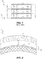
- FIG. 1 One technique in the art to increase displacement in a bulk piezoelectric device 100 is depicted in Figure 1 .
- the bulk device 100 utilizes a plurality of bulk piezoelectric material slabs 135A, B, C (e.g., with T 1 of each slab being > 50 ⁇ m in (z) thickness) stacked up in an alternating manner with a plurality of electrodes 110, 120, 130, 140.
- voltage biasing of the electrodes is such that the electric field applied across each successive piezoelectric slab is in an opposite direction as that of the subjacent and superjacent slab.
- a positive voltage is applied to electrodes 110 and 130 while a negative voltage is applied to electrodes 120 and 140.
- This biasing may be used first to pole the bulk piezoelectric slabs into opposing polarization (e.g., slabs 135A and 135C having polarization P 1 in a first direction, and slab 135B having a polarization P 2 in second direction opposite P 1 and P 3 ).
- This same biasing may then be used to impart a time varying electric field across the slabs that induces a large cumulative physical displacement.
- Patent application US2009026887 A1 describes, in a piezoelectric device, a first electrode, a first piezoelectric film, a second piezoelectric film, and a second electrode are formed in this order on a first electrode formed above a surface of the substrate, and an intermediate electrode is arranged between the first and second piezoelectric films.
- Each of the first and second piezoelectric films has a thickness of 10 micrometers or smaller, and has a first surface facing toward the substrate and a second surface opposite to the first surface. At least one of the first and second surfaces has an arithmetic average surface roughness (Ra) of 0.5 micrometers or smaller.
- Thin film piezoelectric devices can be advantageously fabricated inexpensively to exceedingly high dimensional tolerances using various micromachining techniques (e.g., material deposition, lithographic patterning, feature formation by etching, etc.).
- one or more piezoelectric thin film device may be fabricated into Microelectromechanical systems (MEMS) that may further include one or more integrated circuit (IC) fabricated with compatible techniques.
- MEMS Microelectromechanical systems
- IC integrated circuit
- a microfluidic device including one or more fluidic chambers and piezoelectric pumping actuators, can be formed in a single printer head die.
- an ultrasonic transducer including an array of piezoelectric membranes capable of generating a high frequency pressure wave in a propagation medium (e.g., air, water, or body tissue) in contact with an exposed outer surface of the transducer element, can be formed in a single MEMS transducer die.
- a propagation medium e.g., air, water, or body tissue
- the thickness of piezoelectric thin film material may be limited by one or more aspects of the thin film fabrication process (e.g., film deposition constraints).
- the relationship between displacement of the piezoelectric material in the presence of an electric field of a given strength and the thickness of the piezoelectric film may not be readily exploited in the same manner as for the bulk piezoelectric device 100.
- limitations on the thickness of the piezoelectric thin film can limit the performance of a thin film piezoelectric device. Structures and techniques that enable greater piezoelectric thin film thicknesses, and therefore enable greater degrees of freedom with respect to designed membrane displacement, are therefore commercially advantageous.
- the invention relates to a thin film piezoelectric device, comprising: a piezoelectric element including: a lower electrode disposed over a first region of a substrate; a first piezoelectric layer having a first polarization disposed over the lower electrode; a second piezoelectric layer having the first polarization disposed over the first piezoelectric layer; an intervening layer disposed between the first and second piezoelectric layers in at least a portion of the first region, wherein the intervening layer is of a different composition than that of the first and second piezoelectric layers, wherein the intervening layer comprises a first layer that interfaces the first piezoelectric layer, a second layer that interfaces the second piezoelectric layer, and a third layer between the first layer and the second layer, and wherein each of the first layer and the second layer is at least one of Pt, Ir, an alloy thereof, or an oxide thereof, wherein the first layer is in direct contact with the first piezoelectric layer, the second layer is in direct contact with the second pie
- the invention also relates to a piezoelectric apparatus, comprising a substrate; an array of piezoelectric elements disposed over the substrate, wherein each piezoelectric element comprises: a first electrode disposed over a first region of a substrate; a first piezoelectric layer having a first polarization disposed over the first electrode; a second piezoelectric layer having the first polarization disposed over the first piezoelectric layer; and an intervening layer disposed between the first and second piezoelectric layers in at least a portion of the first region, wherein the intervening layer is of a different composition than that of the first and second piezoelectric layers, wherein the intervening layer comprises a first layer that interfaces the first piezoelectric layer, a second layer that interfaces the second piezoelectric layer, and a third layer between the first layer and the second layer, and wherein each of the first layer and the second layer is at least one of Pt, Ir, an alloy thereof, or an oxide thereof, wherein the first layer is in direct contact with the
- the invention also relates to a method comprising: operating a piezoelectric element of a thin film piezoelectric device, the piezoelectric element including: a lower electrode disposed over a first region of a substrate; a first piezoelectric layer having a first polarization disposed over the lower electrode; a second piezoelectric layer having the first polarization disposed over the first piezoelectric layer; an intervening layer disposed between the first and second piezoelectric layers in at least a portion of the first region, wherein the intervening layer is of a different composition than that of the first and second piezoelectric layers, said intervening layer functioning as an inner electrode comprising conductive material capable of sustaining a voltage different than that of the lower electrode, wherein the intervening layer comprises a first layer that interfaces the first piezoelectric layer, a second layer that interfaces the second piezoelectric layer, and a third layer between the first layer and the second layer, and wherein each of the first layer and the second layer is at least one of Pt,
- Multi-layered thin film piezoelectric material stacks and devices incorporating such stacks are described herein.
- the thin film piezoelectric material stacks are disposed over a substrate, such as, but not limited to a semiconductor wafer.
- the piezoelectric material layers in a multi-layered stack have substantially the same composition across all piezoelectric layers.
- an intervening material layer is disposed between two successive piezoelectric material layers in at least a portion of the area of a substrate over which the multi-layered piezoelectric material stack is disposed.
- the intervening material may serve one or more function within the stack including, but not limited to, inducing an electric field across one or both of the successive piezoelectric material layers, inducing a discontinuity in the microstructure between the two successive piezoelectric materials, modulating a cumulative stress of the piezoelectric material stack, and serving as a basis for varying the strength of an electric field as a function of location over the substrate.
- a thin film piezoelectric material stack includes at least a first and second piezoelectric material layer having anisotropic polarization with poles oriented in substantially the same direction for both layers.
- thin film piezoelectric material stack includes at least a first and second piezoelectric material layer having columnar polycrystalline microstructure.
- a multi-layered thin film piezoelectric material stack includes at least three conductive electrode layers including at least one inner electrode layer disposed between two piezoelectric material layers.
- at least one outer electrode layer is disposed on a side of at least one of the piezoelectric layers opposite of the inner electrode layer.
- a first piezoelectric material layer is disposed between the inner electrode layer and a lower electrode layer while a second piezoelectric material layer is disposed over the inner electrode layer.
- the second piezoelectric material layer is disposed between the inner electrode layer and an upper electrode layer with the first piezoelectric material layer is disposed under the inner electrode layer.
- the first piezoelectric material layer is between the inner electrode layer and an lower electrode layer while a second piezoelectric material layer is disposed between the inner electrode layer an a upper electrode layer.
- a multi-layered thin film piezoelectric material stack is displaced through application of a time varying voltage across two of three electrodes while the third electrode is biased so as to drop approximately half of the electric field across two layers of piezoelectric material.
- the third of the three electrodes is maintained at a fixed or time varying bias potential.
- the bias potential is intermediate of peak-to-peak voltages applied across the two electrodes over an entire phase of the time varying drive voltage.
- a fixed ground potential is maintained while the time varying voltages applied to the driven electrodes vary symmetrically with respect to ground potential.
- a piezoelectric micromachined transducer array for example suitable for the ultrasonic band, includes a plurality of transducer elements, each of which includes a multi-layered piezoelectric thin film stack.
- a piezoelectric fluidic pumping array for example suitable for use in a print head, includes a plurality of pumping chambers, each of which are in fluid communication with a multi-layered piezoelectric thin film stack.
- Coupled is used herein to describe functional or structural relationships between components. “Coupled” may be used to indicate that two or more elements are in either direct or indirect (with other intervening elements between them or through the medium) mechanical, acoustic, optical, or electrical contact with each other, and/or that the two or more elements co-operate or interact with each other (e.g., as in a cause and effect relationship).
- the terms “over,” “under,” “between,” and “on” as used herein refer to a relative position of one component or material layer with respect to other components or layers where such physical relationships are noteworthy for mechanical components in the context of an assembly, or in the context of material layers of a micromachined stack.
- One layer (component) disposed over or under another layer (component) may be directly in contact with the other layer (component) or may have one or more intervening layers (components).
- one layer (component) disposed between two layers (components) may be directly in contact with the two layers (components) or may have one or more intervening layers (components).
- a first layer (component) "on” a second layer (component) is in direct contact with that second layer (component).
- Figure 2 is a cross-sectional view of a thin film piezoelectric device 200 having a piezoelectric material thickness that exceeds a critical thickness, T c .
- the thin film device 200 includes a substrate 202, which may be any substrate conventional to thin film piezoelectric devices. More specifically, the substrate 202 may include one or more material layers, each of any thickness (e.g., thin film or bulk slab materials), but in combination serve as a means of mechanical support to the multi-layer thin film piezoelectric stack.
- the substrate 202 may include one or more thin films, such as dielectrics, disposed over a bulk slab material, such as a semiconductor (e.g., crystalline silicon) wafer.
- films within the substrate 202 may include templating features over which the thin film piezoelectric stack is deposited so as to affect the structure or profile shape of the piezoelectric stack.
- a bottom electrode 210 Disposed over the substrate 202 is a bottom electrode 210, which may comprise one or more metals in laminated and/or alloyed form.
- the electrode layer 210 may be any known in the art to be suitable for forming an overlying piezoelectric material with suitable dipole characteristics.
- the electrode layer 210 may include one or more metal and/or metal oxide thin film layer providing good mechanical adhesion to piezoelectric material and provide suitable conductivity to insure impedance across the area of the electrode layer 210 is sufficiently small for the piezoelectric device 301 to function.
- the electrode layer 210 includes an inert noble metal with high temperature stability and suitable microstructure to promote textured growth of the piezoelectric layer 235.
- at least the surface of the electrode layer 210 interfacing with the piezoelectric material layer 235 has crystal texture (the distribution of crystallographic orientations in a polycrystalline material) where the preferred orientation is (111). Such texture has been found to promote desired microstructure in the piezoelectric layer 235.
- Exemplary interfacial electrode layer materials include Pt, Ni, and Ir, alloys thereof (e.g., IrTiW, TiPt, etc.), and oxides thereof (e.g., IrO 2 , NiO 2 , PtO 2 , etc.).
- a layer of Pt, Ir, an alloy thereof, or oxide thereof is disposed over a Ti, W, or TiW layer, which provides good conductivity and is typically of relatively low stress (e.g., ⁇ 200 MPa). While the total thickness of the electrode layer 210 may vary, an exemplary range is 0.1-0.2 ⁇ m.
- the piezoelectric film layer 235 may be of any composition known to have crystal forms lacking inversion symmetry (i.e., are polarized), and thereby display the solid-state charge-stress relationship known as the piezoelectric effect.
- the piezoelectric material layer 235 is Lead Zirconate Titanate (PZT), and more particularly polycrystalline PZT having crystal texture that favors the perovskite structure.
- PZT Lead Zirconate Titanate
- Various dopants may be included in the PZT, such as, but not limited to, niobium.
- the piezoelectric layer 235 is generally deposited using some technique typical of thin film processing, such as, but not limited, to RF magnetron, reactive physical vapor deposition (PVD).
- PVD reactive physical vapor deposition
- the deposition process and the interface of surface of the bottom electrode 210 have a significant impact on the composition and microstructure of the piezoelectric layer 235 and while good piezoelectric properties have been achieved for a nominal piezoelectric layer thickness, it has been further found by the inventors that when the deposition thickness exceeds a critical thickness, the physical and/or electrical properties of the deposited film degrades.
- large stress e.g., > 1 GPa
- large stress present in the piezoelectric layer 235 can bow the substrate (a compressive stress is illustrated in Figure 2 ) and/or induce cracks 217 throughout the thickness of the layer 235 after exceeding a threshold.
- break down voltage has found to drop when the piezoelectric layer 235 has too great of thickness.
- the inventors have found that grain size of columnar PZT increases with increasing thickness of the piezoelectric layer 235. Although not bound by theory, it is currently theorized that the larger grain boundaries that form as grain size increases results in the cracks and breakdown voltage degradation that is seen with layers that are sputter deposited to thicknesses over the critical thickness.
- a thin film piezoelectric stack includes at least a pair of thin film piezoelectric layers separated by an intervening material layer.
- the intervening layer may serve one or more function within the piezoelectric material stack including, but not limited to, inducing an electric field across one or both of the successive piezoelectric material layers, inducing a discontinuity in the microstructure between the two successive piezoelectric material layer, modulating a cumulative stress of the piezoelectric material stack, and serving as a basis for varying the strength of an electric field across the two piezoelectric material layers as a function of location over the substrate.
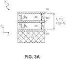
- FIG. 3A is a cross-sectional view of one such multi-layered thin film piezoelectric device 301 employing first and second piezoelectric thin film layers 315, 325 separated by an intervening material layer 320, in accordance with an embodiment.
- each of the piezoelectric materials layers 315, 325 have a thickness (e.g., T 2 ) that is below the critical thickness T c (e.g. 4 ⁇ m), but their combined thickness is greater than T c , thereby making a greater total thickness of piezoelectric available to the micromachining techniques leveraged in thin film piezoelectric devices.
- This greater total thickness may in turn provide a larger electro-mechanical response by the piezoelectric device 301 than otherwise possible with a reduced thickness of thin film piezoelectric material.
- each of the piezoelectric layers 315, and 325 has a thickness below 10 ⁇ m, advantageously 1-4 ⁇ m for PZT embodiments, and most advantageously about 1-2 ⁇ m for PZT embodiments displaying highest breakdown voltages.
- the total piezoelectric thickness may be 4 ⁇ m, or more, while overcoming the limitations described for single layers in the context of Figure 2 . Indeed, this approach has achieved in certain embodiments a total PZT thicknesses of up to 8 ⁇ m with no film cracking and breakdown voltages remaining sufficiently high for any application into at least the 6-7 ⁇ m range.
- sputtered piezoelectric films may have breakdown voltages greater than or equal to 1 MV/cm for thicknesses less than Tc, and less than or equal to 500 kV/cm for thicknesses greater than Tc.
- bulk PZT may have breakdown voltages on the order of a few hundred kV/cm.
- the multi-layered structure depicted in Figure 3A can be fabricated with highly conformal and controlled processes (e.g., PVD), membranes of any size, shape, or surface topography (e.g., flat surface, domes, dimpled, etc.) may be fabricated. Therefore, substantially any device employing a single thin film piezoelectric layer can be fabricated with a multi-layered stack, such as that depicted in Figure 3A .
- sputtered piezoelectric layers can have higher Curie temperatures than bulk or sol-gel piezoelectric layers. For example, sputtered piezoelectric layers can withstand processing temperatures up to about 500°C without depoling versus around 200°C for bulk and sol-gel piezoelectric layers.
- a multi-layer thin film piezoelectric stack is disposed over a first region of a supporting substrate 202, which may be any of those substrates described in the context of Figure 2 as the same reference number is retained throughout this description for structures having like properties.
- a first electrode layer 210 Disposed over the substrate 202 is a first electrode layer 210 having any of those compositions and structures previously described.
- the multi-layered piezoelectric stack is disposed on (i.e., in direct or intimate contact with) the electrode layer 210.
- the first and second piezoelectric thin film layers 315, 325 may be of a same or different composition.
- all the piezoelectric layers within a stack are PZT.
- At least one of the piezoelectric material layers may have another composition, such as but not limited to, III-N materials, such as aluminum nitride (A1N) and gallium nitride (GaN), both of which display piezoelectric effect when in the wurtzite structure.
- III-N materials such as aluminum nitride (A1N) and gallium nitride (GaN), both of which display piezoelectric effect when in the wurtzite structure.
- BaTiO 3 , or even polyvinylidene difluoride (PVDF) polymer particles may be utilized in one or more of the piezoelectric layers 315 and 325.
- the piezoelectric layers within the multi-layered stack all have the same direction of polarization.
- the piezoelectric layer 315 has a columnar microstructure relative to the substrate 202 and this film, as deposited in Figure 3A , has permanent polarization. With permanent polarization, no poling is performed to induce the piezoelectric effect in contrast to a bulk material or sol-gel. Sputtered piezoelectric layers are poled as they are deposited (e.g. by PVD) on an electrode layer 210.
- the polarization field within the piezoelectric layer 315 has a direction (orientation) that is perpendicular to the substrate 202.
- the perpendicular polarization field may be in one of the two directions perpendicular to the substrate 202, as denoted by the polarization field arrows P A in Figure 3A .
- the perpendicular polarization field within the piezoelectric layer 325 is also in one of the two directions perpendicular to the substrate 202, as denoted by the polarization field arrows P B in Figure 3A .
- a second, or "top” electrode material layer 330 Disposed over the piezoelectric layer 325 is a second, or "top" electrode material layer 330, which may include any of the same materials and/or structures described for the electrode 210.
- a noble metal layer such as one containing any of Au, Pt, or Ir, is disposed on the surface of the piezoelectric layer 325.
- a Ti, W, or TiW layer is disposed underneath the noble metal layer, for example to provide good adhesion to the piezoelectric layer. While the total thickness of the top electrode material layer 330 may vary, an exemplary range is 0.1-0.2 ⁇ m.
- the intervening layer 320 is generally of a different composition than that of piezoelectric layers 315, 325.
- the intervening layer 320 is a material that disrupts the grain structure of the piezoelectric material layer 315, but serves as a good interface with both the piezoelectric material layers 315 and 325. Disruption of the grain structure is to limit the grain/boundary size within the piezoelectric layer 325.
- the intervening layer 320 has good adhesion to both the piezoelectric material layers 315 and 325 and further provides an interface to the piezoelectric material layer 325 that promotes the crystallinity desired for piezoelectricity (e.g., perovskite where the piezoelectric layer 325 is PZT).
- Intervening materials include those utilized for the interface of the piezoelectric material layer 315 and the electrode layer 210, such as, Pt, Ni, and Ir, alloys thereof (e.g., IrTiW, TiPt, etc.), and oxides thereof (e.g., IrO 2 , NiO 2 , PtO 2 , etc.). While thickness of the intervening layer 320 may vary, exemplary thicknesses are below 0.15 ⁇ m and may be as low as few tens of nanometers.
- the intervening layer 320 further serves as an inner electrode comprising conductive material capable of sustaining a voltage different than that of the electrode 210.
- Figure 3B is a cross-sectional view of a multi-layered thin film piezoelectric device 302 employing such an intervening electrode, in accordance with an embodiment. As such, the device 302 retains the properties of the device 301 with the additional aspect that the intervening layer 320 is to sustain a bias or reference voltage potential relative to the electrodes 210 and 330, which in this context are referred to herein as "outer" electrodes while the intervening layer 320 is an "inner" electrode.
- Intervening layer 320 comprises a Pt, Ni, and Ir, alloy thereof, and oxide thereof (e.g., IrO 2 , NiO 2 , PtO 2 ), in intimate contact with both the piezoelectric layer 315 and 325.
- Such layers are further separated by a an intervening metal layer with greater bulk conductivity, lower stress, or otherwise satisfying one or more other electrode design criteria.
- a Ti, W, or TiW material may be inserted between two Ir, or Ir oxide, layers, one that interfaces to the piezoelectric layer 315, and the other that interfaces to the piezoelectric layer 325.
- thickness of the intervening layer 320 when further serving as an inner electrode may vary, exemplary thicknesses are between 0.1 ⁇ m and 0.2 ⁇ m.
- Figure 3B further illustrates an electrical drive signal suitable for a multi-layered piezoelectric stack where both piezoelectric thin films have the same direction of polarization.
- the inner electrode(s) are to be at a potential that is intermediate to the peak-to-peak voltages applied across the outer electrodes. This intermediate potential may be maintained over the entire phase of the time varying voltage applied across the outer electrodes.
- the intervening layer 320 is an electrode layer maintained at ground potential.
- the electric field applied across each of the piezoelectric layers 315 and 325 remains oriented in the same direction so that the electro-mechanical effects of each piezoelectric layer are in phase with the other.
- FIG. 3C is a cross-sectional view of the multi-layered thin film piezoelectric device 303 that has substantially the same structure as that described for Figure 3B , but further illustrates an operational biasing of the intervening layer 320, in accordance with an embodiment.
- V bias DC bias potential
- V bias may be a fixed or varying positive and/or negative voltage with respect to a ground reference potential.
- a multi-layered piezoelectric thin film stack includes a plurality of intervening layers, at least two of which are separated by an intervening piezoelectric layer.
- Figure 3D is a cross-sectional view of a multi-layered thin film piezoelectric device 304 employing a plurality of intervening material layers 320A, 320B, and 320C. As depicted, the device 304 employs an extension of the bi-layered piezoelectric stack depicted in the device 302 to illustrate how an even greater piezoelectric thicknesses may be achieved while still maintaining film quality.
- Figure 3D further illustrates how a plurality of intervening layers may be electrically driven following the guideline that inner electrodes are driven/biased so as to ensure a portion of the field generated across the outer electrodes 210, 330 is dropped across the each of piezoelectric thin film layers 315, 325, 335, 345.
- the composition and thicknesses of the piezoelectric thin film layers 335 and 345 may be any of those described elsewhere herein for the layers 315 and 325, for example to have all piezoelectric layers 315-345 of a same composition and thickness (e.g., all being less than the critical thickness T c ), although the composition and thickness might also vary across the piezoelectric film layers.
- each of the intervening layers 320A, 320B, and 320C may have any of the compositions described elsewhere for the intervening layer 320.
- each intervening layer forms an Ir or Ir oxide interface with the adjacent piezoelectric layers.
- the polarization direction in each piezoelectric film layer 315, 325, 335, 345 is the same, and permanent, (e.g., each being an RF magnetron reactive sputter-deposited PZT).
- each intervening layer further functions as an inner electrode
- the electrical drive signal to the various electrodes may take the form further illustrated in Figure 3D where the voltage potentials applied to the inner electrodes increment between peak voltages applied across the outer electrodes 210, 330.
- a resistor network may be utilized to induce a first IR drop between the electrode 210 and intervening layer 320A and induce a second IR drop (e.g., equal to that of the first IR drop) between the electrode 330 and intervening layer 320C.
- the intervening electrode 320B may then be maintained at ground potential, as depicted, or otherwise biased appropriately relative to the time varying voltages applied so as to align the electric fields across the piezoelectric material layers 325 and 335 with those across the piezoelectric material layers 315 and 345.
- the intervening layer spans a smaller area than does at least one of a lower electrode, an upper electrode, and/or the adjacent piezoelectric layers.
- one piezoelectric layer is disposed directly on another piezoelectric layer where the intervening layer is absent.
- Such embodiments may achieve many, if not all, of the benefits of the stacked multi-layered piezoelectric structures described herein even though in certain device regions the layered piezoelectric comprises two material layers that may be of substantially the same composition in direct contact and with a total thickness that exceeds the critical thickness where properties of a continuous film degrade.
- Figure 4A is a cross-section view of a multi-layered thin film piezoelectric device 401 employing a patterned intervening layer 320, in accordance with an embodiment.
- the intervening layer 320 spans only a portion of the surface area (x-y plane) of the substrate 202 that is covered by the electrode 210, where layers 315, 325 are in contact with one another in a region of no more than a critical dimension CD s which is at least equal to the thickness of one of the piezoelectric layers (e.g. layer 325 in this example).
- the contact region being less than CDs in length reduces the possibility of voids between layers 315, 325.
- the adhesion provided by the presence of intervening layer 320, albeit in reduced proportion relative to the embodiments depicted in Figures 3A-3C , and/or beneficial grain discontinuity, and/or strain concentration or other mode of piezoelectric stress reduction imparted by the intervening layer edge 321 may permit the piezoelectric material to achieve the greater combined thickness without detrimental effects of cracking, etc.
- the patterned intervening layer may serve as a basis for varying the strength of an electric field as a function of location over the substrate 202.
- the patterned intervening layer may be biased relative to the outer electrodes so as to induce the entire electric field across only one of the first and second piezoelectric materials, while in regions where the intervening layer is absent the field will drop across the total thickness of both first and second piezoelectric materials.
- a piezoelectric membrane may be made that includes three or more electrodes (e.g., two outer and one inner electrode) in only a portion of the membrane area, such as one continuous inner portion, or one continuous peripheral portion.
- a piezoelectric membrane may include only two electrodes (e.g., top and bottom electrodes) but with an intervening material in a continuous inner or peripheral portion, or in discontinuous portions of the membrane area.
- the intervening material may enable a thicker piezoelectric material in spaces between regions where there is an intervening material.
- Figure 4B is a plan view of the patterned intervening layer 320 of the multi-layered thin film piezoelectric device 401, in accordance with embodiments.
- the patterned intervening layer 320 forms a mesh of electrically continuous material, which, for example, may be biased to a reference (ground) potential as depicted in Figure 4A .
- the structure of patterned intervening layer 320 may also serve to reduce stress of the piezoelectric stack, for example.
- the device 401 may then include a piezoelectric membrane that spans a plurality of the openings 450.
- the area depicted in Figure 4B may span a plurality of piezoelectric devices with a single piezoelectric membrane formed with double thickness at each opening 450.
- a first outer electrode e.g., 210
- a second outer electrode e.g., 330
- the critical dimension of the region where the piezoelectric layers 315, 325 are in direct contact can be as large as the dimension of the piezoelectric membrane needed for the device application (e.g., CD s >CD of one membrane)
- the addition of the patterned intervening layer 320 amounts only to an extra film deposition and patterning operation relative to a conventional single piezoelectric film layer with design and operation of the membrane be nearly the same as that of a continuous double thickness of piezoelectric material.
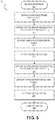
- FIG. 5 is a flow diagram illustrating a method 501 of fabricating a multi-layered thin film piezoelectric device, in accordance with an embodiment.
- the method 501 begins at operation 502 with receipt of a suitable substrate, such as any of those described elsewhere herein in the context of substrate 202.
- a lower electrode metal thin film layer or stack is deposited, by any of PVD, chemical vapor deposition (CVD), or atomic layer deposition (ALD).
- CVD chemical vapor deposition
- ALD atomic layer deposition
- PVD is employed to deposit a metal stack including a Ti, W, or TiW layer and a noble metal interface layer, such as Pt, Ir, or Ir oxide, disposed on the Ti, W, or TiW layer.
- a first polarized piezoelectric thin film is deposited directly on the noble metal interface of the lower electrode to a thickness below the threshold, or critical thickness.
- a PVD process is utilized at operation 515. More specifically, PZT is deposited with an RF magnetron reactive PVD process performed at an elevated temperature (e.g., greater than 400°C). With such a process, the PZT as-deposited is polarized and has a high Curie temperature (e.g., more than 100°C higher than a conventional films requiring poling).
- the method 501 proceeds to operation 520 where an intervening layer is deposited.
- the intervening layer includes a noble metal layer such as Pt, or Ir, or Ir oxide, disposed on the piezoelectric material formed at operation 515.
- a greater conductive metal thickness is achieved through PVD of a first noble metal layer such as, but not limited to, Pt, Ir, or Ir oxide, followed by PVD deposition of W, Ti, or TiW layer, which is then followed by a PVD of a second noble metal layer such as, but not limited to, Pt, Ir, or Ir oxide.
- the middle electrode metal thin film layer(s) is then patterned at operation 521, for example with any conventional photolithography and etch process.
- the patterning reduces the area of the middle electrode to be less than the area occupied by the piezoelectric material formed at operation 515.
- the patterning operation 521 exposes a portion of the first piezoelectric layer.
- a second polarized piezoelectric thin film is deposited to a thickness below some threshold, or critical thickness (T c ).
- T c critical thickness
- operation 525 is essentially a repetition of the operation 521, depositing the same material (e.g., PZT) to a same thickness (e.g., 2-4 ⁇ m).
- operation 530 entails PVD deposition of a noble metal layer such as, but not limited to, Au, Pt, Ir, or Ir oxide, deposited on a W, or TiW layer, also deposited by PVD.
- a noble metal layer such as, but not limited to, Au, Pt, Ir, or Ir oxide
- the top electrode metal thin film layer(s) is then patterned at operation 531, for example with any conventional photolithography and etch process. The patterning reduces the area of the top electrode to be less than the area occupied by the piezoelectric material formed at operation 525. In other words, the patterning operation 531 exposes a portion of the second piezoelectric layer.
- the upper electrode is patterned to be disposed within a region where the first and second piezoelectric films are in direct contact (e.g., as depicted in Figure 4A ).
- the operations 525-531 may be repeated cyclically until a desired total thickness of piezoelectric material is obtained.
- the lower electrode may be patterned just as described for the top electrode in addition to, or instead of, the patterning operation 531.
- Figure 6A is a plan view of a pMUT array 600, in accordance with an embodiment.
- Figure 6B is a cross-sectional view of a pMUT transducer element employing a multi-layered thin film piezoelectric membrane that is used in the array 600, in accordance with an embodiment.
- Figure 6C is a schematic of an ultrasonic transducer apparatus employing the pMUT array 600.
- the array 600 includes a plurality of drive/sense electrode stacks 130 disposed over an area defined by a first dimension, x and a second dimension y, of the substrate 202.
- the drive/sense electrode rail stack 130 repeats an interdigitated ted electrode layout with additional cells forming a 1D electrode array of arbitrary size (e.g., 128, 256, etc.).
- Each of the drive/sense electrode rail stacks is electrically addressable independently from any other drive/sense electrode rail stacks arrayed over the substrate 202.
- a pMUT array includes a plurality of piezoelectric transducer element populations.
- Each piezoelectric transducer element population operates as a group associated with a frequency response that is a composite of the individual transducer elements 602 within each element population.
- each piezoelectric transducer element 602 includes a multi-layered thin film piezoelectric membrane. While the piezoelectric membrane may generally be of any shape conventional in the art, in exemplary embodiments the piezoelectric membrane has rotational symmetry.
- each transducer element 602 includes a piezoelectric membrane having a circular geometry.
- the piezoelectric membrane may further be a spheroid with curvature in a third (z) dimension to form a dome (as further illustrated by Figure 6B ), or a dimple. Planar membranes are also possible.
- the drive/sense electrode rail stack which may include an inner electrode 620 in some embodiments, and a multi-layered piezoelectric membrane, is depicted in the cross-sectional view of Figure 6B .
- a convex transducer element 602 includes a top surface 604 that during operation forms a portion of a vibrating outer surface of the pMUT array 600.
- the transducer element 602 also includes a bottom surface 606 that is attached to a top surface of the substrate 202.
- the transducer element 602 includes a convex or dome-shaped multi-layered piezoelectric membrane including thin film layers 615 and 625 disposed on either side of the inner electrode 620 and further surrounded by the drive/sense electrodes 610 and 630.
- the multi-layered piezoelectric membrane can be formed by depositing (e.g., sputtering) piezoelectric material particles in uniform layer 615, 625 on a profile-transferring substrate (e.g., photoresist) that has a dome formed on a planar top surface, for example.
- the transducer element 602 can optionally include a thin film layer 622, such as silicon dioxide that can serve as a support and/or etch stop during fabrication.
- a dielectric membrane 624 may further serve to insulate the various vertically stacked electrode metallization.
- a vertically-oriented electrical interconnect 626 connects the drive/sense electrode 610 to drive/sense circuits via the drive/sense electrode rail 611.
- a similar interconnect 632 connects the electrode 630 while the inner electrode 620 may be patterned (e.g., in the y-dimension) to couple multiple transducer element inner electrodes to a same bias/reference potential.
- An annular support 636 surrounding a cavity 641 with an axis of symmetry defining a center of the transducer element 602, mechanically couples the multi-layered piezoelectric membrane to the substrate 202.
- the support 636 may be of any conventional material, such as, but not limited to, silicon dioxide, polycrystalline silicon, polycrystalline germanium, SiGe, and the like. Exemplary thicknesses of support 636 range from 10-50 ⁇ m and exemplary thickness of the membrane 624 range from 2-20 ⁇ m.
- FIG. 6C is a functional block diagram of an ultrasonic transducer apparatus 675 that employs the pMUT array 600, in accordance with an embodiment of the present invention.
- the ultrasonic transducer apparatus 675 is for generating and sensing pressure waves in a medium, such as water, tissue matter, etc.
- the ultrasonic transducer apparatus 675 has many applications in which imaging of internal structural variations within a medium or multiple media is of interest, such as in medical diagnostics, product defect detection, etc.
- the apparatus 675 includes at least one pMUT array 600, which may be any of the pMUT arrays described elsewhere herein having any of the transducer element and element population attributes described.
- the pMUT array 600 is housed in a handle portion 678 which may be manipulated by machine or by a user of the apparatus 675 to change the facing direction and location of the outer surface of the pMUT array 600 as desired (e.g., facing the area(s) to be imaged).
- Electrical connector 680 electrically couple channels of the pMUT array 600 to a communication interface external to the handle portion 678.
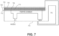
- FIG. 7 is a cross-sectional view of a micromachined piezoelectric fluidic pumping apparatus, in accordance with an embodiment of the present invention.
- ink is provided by a frame flow path 712 that leads to the bottom surface 715 of the substrate.
- Acoustic energy is applied to the ink pumping chamber by a multi-layered thin film piezoelectric membrane 704.
- the membrane 704 includes first and second piezoelectric thin film layers 715 and 725 separated by an intervening material layer 720 (which may further function as an inner electrode).
- electrodes 710 and 730 are driven with a time vary voltage (e.g., pulse) that displaces the membrane 704 relative to the bottom surface 715 and thereby displaces ink from within the pumping chamber out of the nozzle, and/or from within the flow path 712 into the pumping chamber.
- a time vary voltage e.g., pulse
- any of the multi-layered thin film piezoelectric membranes described elsewhere herein may be utilized for the membrane 704.
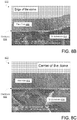
- Figures 8A , 8B and 8C show respective cross-sectional views 800, 810, 820 of a sputtered thin film piezoelectric device having a columnar structure according to an embodiment.
- the device variously represented in views 800, 810, 820 may have some or all of the features of a sputtered thin film piezoelectric device discussed herein.
- such a device may include features variously found in some or all of piezoelectric devices 302, 303, 304, transducer element 602 and/or the like.
- a silicon substrate 804 of the device may have disposed thereon an electrode 806 and a piezoelectric thin film 802.
- thin film 802 forms at least part of a dome structure over a bump in substrate 804.
- View 810 provides a more detailed view of one edge of the dome structure
- view 820 provides a more detailed view of the center of the dome structure.
- additional processing - subsequent to the stage of processing represented in views 800, 810, 820 - may be performed to alter on some or all of thin film 802, substrate 804 and electrode 806.
- FIGS 800, 810, 820 variously show that piezoelectric thin film 802 has polycrystalline microstructures which are substantially columnar, relative to the surface of substrate 804.
- grain size of columnar PZT increases with increasing thickness of the piezoelectric layer, and the larger grain boundaries that form as grain size increases have been associated with cracks and breakdown voltage degradation for PZT layers that are sputter deposited to thicknesses over a critical thickness.
Landscapes
- Engineering & Computer Science (AREA)
- Manufacturing & Machinery (AREA)
- General Electrical Machinery Utilizing Piezoelectricity, Electrostriction Or Magnetostriction (AREA)
- Transducers For Ultrasonic Waves (AREA)
- Particle Formation And Scattering Control In Inkjet Printers (AREA)
Description
- Embodiments of the invention generally relate to piezoelectric devices, and more specifically pertain to thin film piezoelectric actuators and transducers.
- Piezoelectric devices find many applications as electro-mechanical actuators and transducers. Piezoelectric devices may be further classified as either employing a bulk piezoelectric material, or a piezoelectric thin film. A bulk piezoelectric material generally has a thickness over 20 microns (µm), and often well over 50 µm, while thin film devices employ a piezoelectric membrane that is less than 15 µm in thickness.
- Generally, physical displacement of a piezoelectric material in the presence of an electric field of a given strength is a function of the thickness of the piezoelectric film. One technique in the art to increase displacement in a bulk
piezoelectric device 100 is depicted inFigure 1 . Thebulk device 100 utilizes a plurality of bulkpiezoelectric material slabs 135A, B, C (e.g., with T1 of each slab being > 50 µm in (z) thickness) stacked up in an alternating manner with a plurality ofelectrodes Figure 1 , voltage biasing of the electrodes is such that the electric field applied across each successive piezoelectric slab is in an opposite direction as that of the subjacent and superjacent slab. For example, at a given instant in time a positive voltage is applied toelectrodes electrodes slabs 135A and 135C having polarization P1 in a first direction, and slab 135B having a polarization P2 in second direction opposite P1 and P3). This same biasing may then be used to impart a time varying electric field across the slabs that induces a large cumulative physical displacement. - Patent application
US2009026887 A1 describes, in a piezoelectric device, a first electrode, a first piezoelectric film, a second piezoelectric film, and a second electrode are formed in this order on a first electrode formed above a surface of the substrate, and an intermediate electrode is arranged between the first and second piezoelectric films. Each of the first and second piezoelectric films has a thickness of 10 micrometers or smaller, and has a first surface facing toward the substrate and a second surface opposite to the first surface. At least one of the first and second surfaces has an arithmetic average surface roughness (Ra) of 0.5 micrometers or smaller. - Thin film piezoelectric devices can be advantageously fabricated inexpensively to exceedingly high dimensional tolerances using various micromachining techniques (e.g., material deposition, lithographic patterning, feature formation by etching, etc.). As such, one or more piezoelectric thin film device may be fabricated into Microelectromechanical systems (MEMS) that may further include one or more integrated circuit (IC) fabricated with compatible techniques. As one example, a microfluidic device, including one or more fluidic chambers and piezoelectric pumping actuators, can be formed in a single printer head die. As another example, an ultrasonic transducer, including an array of piezoelectric membranes capable of generating a high frequency pressure wave in a propagation medium (e.g., air, water, or body tissue) in contact with an exposed outer surface of the transducer element, can be formed in a single MEMS transducer die.
- One issue with conventional thin film piezoelectric materials is that the thickness of piezoelectric thin film material may be limited by one or more aspects of the thin film fabrication process (e.g., film deposition constraints). Thus, the relationship between displacement of the piezoelectric material in the presence of an electric field of a given strength and the thickness of the piezoelectric film may not be readily exploited in the same manner as for the bulk
piezoelectric device 100. As such, limitations on the thickness of the piezoelectric thin film can limit the performance of a thin film piezoelectric device. Structures and techniques that enable greater piezoelectric thin film thicknesses, and therefore enable greater degrees of freedom with respect to designed membrane displacement, are therefore commercially advantageous. - The invention relates to a thin film piezoelectric device, comprising: a piezoelectric element including: a lower electrode disposed over a first region of a substrate; a first piezoelectric layer having a first polarization disposed over the lower electrode; a second piezoelectric layer having the first polarization disposed over the first piezoelectric layer; an intervening layer disposed between the first and second piezoelectric layers in at least a portion of the first region, wherein the intervening layer is of a different composition than that of the first and second piezoelectric layers, wherein the intervening layer comprises a first layer that interfaces the first piezoelectric layer, a second layer that interfaces the second piezoelectric layer, and a third layer between the first layer and the second layer, and wherein each of the first layer and the second layer is at least one of Pt, Ir, an alloy thereof, or an oxide thereof, wherein the first layer is in direct contact with the first piezoelectric layer, the second layer is in direct contact with the second piezoelectric layer, and wherein the third layer is one of a Ti, W, or TiW layer; and an upper electrode disposed over the second piezoelectric layer; wherein the piezoelectric element is in fluid communication with a pumping chamber of a microfluidic device, or wherein the piezoelectric element is disposed over a sealed cavity of an ultrasonic transducer.
- The invention also relates to a piezoelectric apparatus, comprising a substrate; an array of piezoelectric elements disposed over the substrate, wherein each piezoelectric element comprises: a first electrode disposed over a first region of a substrate; a first piezoelectric layer having a first polarization disposed over the first electrode; a second piezoelectric layer having the first polarization disposed over the first piezoelectric layer; and an intervening layer disposed between the first and second piezoelectric layers in at least a portion of the first region, wherein the intervening layer is of a different composition than that of the first and second piezoelectric layers, wherein the intervening layer comprises a first layer that interfaces the first piezoelectric layer, a second layer that interfaces the second piezoelectric layer, and a third layer between the first layer and the second layer, and wherein each of the first layer and the second layer is at least one of Pt, Ir, an alloy thereof, or an oxide thereof, wherein the first layer is in direct contact with the first piezoelectric layer, the second layer is in direct contact with the second piezoelectric layer, and wherein the third layer is one of a Ti, W, or TiW layer; and a second electrode disposed over the second piezoelectric layer; wherein each piezoelectric element is in fluid communication with a pumping chamber of a microfluidic device, or each piezoelectric element is disposed over a sealed cavity of an ultrasonic transducer.
- The invention also relates to a method comprising: operating a piezoelectric element of a thin film piezoelectric device, the piezoelectric element including: a lower electrode disposed over a first region of a substrate; a first piezoelectric layer having a first polarization disposed over the lower electrode; a second piezoelectric layer having the first polarization disposed over the first piezoelectric layer; an intervening layer disposed between the first and second piezoelectric layers in at least a portion of the first region, wherein the intervening layer is of a different composition than that of the first and second piezoelectric layers, said intervening layer functioning as an inner electrode comprising conductive material capable of sustaining a voltage different than that of the lower electrode, wherein the intervening layer comprises a first layer that interfaces the first piezoelectric layer, a second layer that interfaces the second piezoelectric layer, and a third layer between the first layer and the second layer, and wherein each of the first layer and the second layer is at least one of Pt, Ir, an alloy thereof, or an oxide thereof, wherein the first layer is in direct contact with the first piezoelectric layer, the second layer is in direct contact with the second piezoelectric layer, and wherein the third layer is one of a Ti, W, or TiW layer; and an upper electrode disposed over the second piezoelectric layer; wherein operating the piezoelectric element includes: driving a time varying voltage across the upper electrode and the lower electrode to place an electric field across the first piezoelectric layer and the second piezoelectric layer; and biasing the inner electrode; wherein the piezoelectric element is in fluid communication with a pumping chamber of a microfluidic device, or wherein the piezoelectric element is disposed over a sealed cavity of an ultrasonic transducer.
- Multi-layered thin film piezoelectric material stacks and devices incorporating such stacks are described herein. The thin film piezoelectric material stacks are disposed over a substrate, such as, but not limited to a semiconductor wafer. In embodiments, the piezoelectric material layers in a multi-layered stack have substantially the same composition across all piezoelectric layers. For certain such embodiments, an intervening material layer is disposed between two successive piezoelectric material layers in at least a portion of the area of a substrate over which the multi-layered piezoelectric material stack is disposed. The intervening material may serve one or more function within the stack including, but not limited to, inducing an electric field across one or both of the successive piezoelectric material layers, inducing a discontinuity in the microstructure between the two successive piezoelectric materials, modulating a cumulative stress of the piezoelectric material stack, and serving as a basis for varying the strength of an electric field as a function of location over the substrate.
- In embodiments, a thin film piezoelectric material stack includes at least a first and second piezoelectric material layer having anisotropic polarization with poles oriented in substantially the same direction for both layers. In embodiments, thin film piezoelectric material stack includes at least a first and second piezoelectric material layer having columnar polycrystalline microstructure.
- In embodiments, a multi-layered thin film piezoelectric material stack includes at least three conductive electrode layers including at least one inner electrode layer disposed between two piezoelectric material layers. For certain such embodiments, at least one outer electrode layer is disposed on a side of at least one of the piezoelectric layers opposite of the inner electrode layer. In one such embodiment, a first piezoelectric material layer is disposed between the inner electrode layer and a lower electrode layer while a second piezoelectric material layer is disposed over the inner electrode layer. In another such embodiment, the second piezoelectric material layer is disposed between the inner electrode layer and an upper electrode layer with the first piezoelectric material layer is disposed under the inner electrode layer. In a third such embodiment, the first piezoelectric material layer is between the inner electrode layer and an lower electrode layer while a second piezoelectric material layer is disposed between the inner electrode layer an a upper electrode layer.
- In embodiments, a multi-layered thin film piezoelectric material stack is displaced through application of a time varying voltage across two of three electrodes while the third electrode is biased so as to drop approximately half of the electric field across two layers of piezoelectric material. In certain such embodiments, the third of the three electrodes is maintained at a fixed or time varying bias potential. In one such embodiment, the bias potential is intermediate of peak-to-peak voltages applied across the two electrodes over an entire phase of the time varying drive voltage. In embodiments, a fixed ground potential is maintained while the time varying voltages applied to the driven electrodes vary symmetrically with respect to ground potential.
- In embodiments, a piezoelectric micromachined transducer array, for example suitable for the ultrasonic band, includes a plurality of transducer elements, each of which includes a multi-layered piezoelectric thin film stack. In embodiments, a piezoelectric fluidic pumping array, for example suitable for use in a print head, includes a plurality of pumping chambers, each of which are in fluid communication with a multi-layered piezoelectric thin film stack.
- Embodiments of the present invention are illustrated by way of example, and not by way of limitation, and can be more fully understood with reference to the following detailed description when considered in connection with the figures, in which:
-
Figure 1 is a cross-sectional view of a conventional bulk piezoelectric device employing a plurality of piezoelectric slabs; -
Figure 2 is a cross-sectional view of a thin film piezoelectric device having a piezoelectric material thickness that exceeds a critical thickness; -
Figure 3A is a cross-sectional view of a multi-layered thin film piezoelectric device employing an intervening material layer, in accordance with an embodiment of the present invention; -
Figure 3B is a cross-sectional view of a multi-layered thin film piezoelectric device employing an intervening electrode, in accordance with an embodiment; -
Figure 3C is a cross-sectional view of the multi-layered thin film piezoelectric device ofFigure 3B further illustrating an operational biasing of the intervening electrode, in accordance with an embodiment; -
Figure 3D is a cross-sectional view of a multi-layered thin film piezoelectric device employing a plurality of intervening material layers; -
Figure 4A is a cross-sectional view of a multi-layered thin film piezoelectric device employing a patterned intervening layer, in accordance with an embodiment; -
Figure 4B is a plan view of the patterned intervening layer in the multi-layered thin film piezoelectric device depicted inFigure 4A , in accordance with an embodiment; -
Figure 5 is a flow diagram illustrating a method of fabricating a multi-layered thin film piezoelectric device, in accordance with an embodiment; -
Figure 6A is a plan view of a piezoelectric micromachined ultrasonic transducer (pMUT) array employing a multi-layered thin film piezoelectric membrane in one or more transducer elements, in accordance with an embodiment; -
Figure 6B is a cross-sectional view of a pMUT transducer element employing a multi-layered thin film piezoelectric membrane, in accordance with an embodiment; -
Figure 6C is a schematic of an ultrasonic transducer apparatus employing a pMUT array having multi-layered thin film piezoelectric membranes, in accordance with an embodiment; and -
Figure 7 is a cross-sectional view of a micromachined piezoelectric fluidic pumping apparatus, in accordance with an embodiment of the present invention. -
Figures 8A ,8B and 8C are respective cross-sectional views of a sputtered thin film piezoelectric device in accordance with an embodiment. - In the following description, numerous details are set forth, however, it will be apparent to one skilled in the art, that the present invention may be practiced without these specific details. In some instances, well-known methods and devices are shown in block diagram form, rather than in detail, to avoid obscuring the present invention. Reference throughout this specification to "an embodiment" means that a particular feature, structure, function, or characteristic described in connection with the embodiment is included in at least one embodiment of the invention. Thus, the appearances of the phrase "in an embodiment" in various places throughout this specification are not necessarily referring to the same embodiment of the invention. Furthermore, the particular features, structures, functions, or characteristics may be combined in any suitable manner in one or more embodiments. For example, a first embodiment may be combined with a second embodiment anywhere the two embodiments are not specifically denoted as being mutually exclusive.
- The term "coupled" is used herein to describe functional or structural relationships between components. "Coupled" may be used to indicate that two or more elements are in either direct or indirect (with other intervening elements between them or through the medium) mechanical, acoustic, optical, or electrical contact with each other, and/or that the two or more elements co-operate or interact with each other (e.g., as in a cause and effect relationship).
- The terms "over," "under," "between," and "on" as used herein refer to a relative position of one component or material layer with respect to other components or layers where such physical relationships are noteworthy for mechanical components in the context of an assembly, or in the context of material layers of a micromachined stack. One layer (component) disposed over or under another layer (component) may be directly in contact with the other layer (component) or may have one or more intervening layers (components). Moreover, one layer (component) disposed between two layers (components) may be directly in contact with the two layers (components) or may have one or more intervening layers (components). In contrast, a first layer (component) "on" a second layer (component) is in direct contact with that second layer (component).
- It is to be understood that while the various embodiments described herein are all presented in a context directly applicable to a microfluidic pumping apparatus or a pMUT array, one or more of the structures or techniques disclosed may be applied to other types of thin film piezoelectric devices. Thus, while the model embodiments have certain synergies and attributes, the disclosure herein has a far broader applicability.
-
Figure 2 is a cross-sectional view of a thin filmpiezoelectric device 200 having a piezoelectric material thickness that exceeds a critical thickness, Tc. Generally, thethin film device 200 includes asubstrate 202, which may be any substrate conventional to thin film piezoelectric devices. More specifically, thesubstrate 202 may include one or more material layers, each of any thickness (e.g., thin film or bulk slab materials), but in combination serve as a means of mechanical support to the multi-layer thin film piezoelectric stack. For example, thesubstrate 202 may include one or more thin films, such as dielectrics, disposed over a bulk slab material, such as a semiconductor (e.g., crystalline silicon) wafer. Other bulk materials, such as glass, or sapphire may also be utilized. As described further elsewhere herein, films within thesubstrate 202 may include templating features over which the thin film piezoelectric stack is deposited so as to affect the structure or profile shape of the piezoelectric stack. Disposed over thesubstrate 202 is abottom electrode 210, which may comprise one or more metals in laminated and/or alloyed form. Generally, theelectrode layer 210 may be any known in the art to be suitable for forming an overlying piezoelectric material with suitable dipole characteristics. More specifically, theelectrode layer 210 may include one or more metal and/or metal oxide thin film layer providing good mechanical adhesion to piezoelectric material and provide suitable conductivity to insure impedance across the area of theelectrode layer 210 is sufficiently small for thepiezoelectric device 301 to function. In further embodiments, theelectrode layer 210 includes an inert noble metal with high temperature stability and suitable microstructure to promote textured growth of thepiezoelectric layer 235. In embodiments, at least the surface of theelectrode layer 210 interfacing with thepiezoelectric material layer 235 has crystal texture (the distribution of crystallographic orientations in a polycrystalline material) where the preferred orientation is (111). Such texture has been found to promote desired microstructure in thepiezoelectric layer 235. Exemplary interfacial electrode layer materials include Pt, Ni, and Ir, alloys thereof (e.g., IrTiW, TiPt, etc.), and oxides thereof (e.g., IrO2, NiO2, PtO2, etc.). In further embodiments where theelectrode layer 210 is a composite stack, a layer of Pt, Ir, an alloy thereof, or oxide thereof, is disposed over a Ti, W, or TiW layer, which provides good conductivity and is typically of relatively low stress (e.g., <200 MPa). While the total thickness of theelectrode layer 210 may vary, an exemplary range is 0.1-0.2 µm. - Disposed on the
bottom electrode 210 is a thickness of piezoelectric material forming the thinpiezoelectric layer 235. Generally, thepiezoelectric film layer 235 may be of any composition known to have crystal forms lacking inversion symmetry (i.e., are polarized), and thereby display the solid-state charge-stress relationship known as the piezoelectric effect. In the exemplary embodiment thepiezoelectric material layer 235 is Lead Zirconate Titanate (PZT), and more particularly polycrystalline PZT having crystal texture that favors the perovskite structure. Various dopants may be included in the PZT, such as, but not limited to, niobium. - The
piezoelectric layer 235 is generally deposited using some technique typical of thin film processing, such as, but not limited, to RF magnetron, reactive physical vapor deposition (PVD). The deposition process and the interface of surface of thebottom electrode 210 have a significant impact on the composition and microstructure of thepiezoelectric layer 235 and while good piezoelectric properties have been achieved for a nominal piezoelectric layer thickness, it has been further found by the inventors that when the deposition thickness exceeds a critical thickness, the physical and/or electrical properties of the deposited film degrades. For example, large stress (e.g., > 1 GPa) present in thepiezoelectric layer 235 can bow the substrate (a compressive stress is illustrated inFigure 2 ) and/or inducecracks 217 throughout the thickness of thelayer 235 after exceeding a threshold. As another example, break down voltage has found to drop when thepiezoelectric layer 235 has too great of thickness. The inventors have found that grain size of columnar PZT increases with increasing thickness of thepiezoelectric layer 235. Although not bound by theory, it is currently theorized that the larger grain boundaries that form as grain size increases results in the cracks and breakdown voltage degradation that is seen with layers that are sputter deposited to thicknesses over the critical thickness. - In embodiments, a thin film piezoelectric stack includes at least a pair of thin film piezoelectric layers separated by an intervening material layer. Generally, the intervening layer may serve one or more function within the piezoelectric material stack including, but not limited to, inducing an electric field across one or both of the successive piezoelectric material layers, inducing a discontinuity in the microstructure between the two successive piezoelectric material layer, modulating a cumulative stress of the piezoelectric material stack, and serving as a basis for varying the strength of an electric field across the two piezoelectric material layers as a function of location over the substrate.
-
Figure 3A is a cross-sectional view of one such multi-layered thin filmpiezoelectric device 301 employing first and second piezoelectric thin film layers 315, 325 separated by an interveningmaterial layer 320, in accordance with an embodiment. Generally, each of the piezoelectric materials layers 315, 325 have a thickness (e.g., T2) that is below the critical thickness Tc (e.g. 4µm), but their combined thickness is greater than Tc, thereby making a greater total thickness of piezoelectric available to the micromachining techniques leveraged in thin film piezoelectric devices. This greater total thickness may in turn provide a larger electro-mechanical response by thepiezoelectric device 301 than otherwise possible with a reduced thickness of thin film piezoelectric material. The thicknesses of thelayers piezoelectric layer 325 may have reduced thickness relative to thepiezoelectric layer 315, and a third piezoelectric layer (not depicted inFigure 3A ) might have a thickness reduced relative to thepiezoelectric layer 325, etc. In embodiments, each of thepiezoelectric layers piezoelectric layers Figure 2 . Indeed, this approach has achieved in certain embodiments a total PZT thicknesses of up to 8 µm with no film cracking and breakdown voltages remaining sufficiently high for any application into at least the 6-7 µm range. For example, sputtered piezoelectric films may have breakdown voltages greater than or equal to 1 MV/cm for thicknesses less than Tc, and less than or equal to 500 kV/cm for thicknesses greater than Tc. By comparison, bulk PZT may have breakdown voltages on the order of a few hundred kV/cm. Notably, because the multi-layered structure depicted inFigure 3A can be fabricated with highly conformal and controlled processes (e.g., PVD), membranes of any size, shape, or surface topography (e.g., flat surface, domes, dimpled, etc.) may be fabricated. Therefore, substantially any device employing a single thin film piezoelectric layer can be fabricated with a multi-layered stack, such as that depicted inFigure 3A . In addition, sputtered piezoelectric layers can have higher Curie temperatures than bulk or sol-gel piezoelectric layers. For example, sputtered piezoelectric layers can withstand processing temperatures up to about 500°C without depoling versus around 200°C for bulk and sol-gel piezoelectric layers. - As shown in
Figure 3A , a multi-layer thin film piezoelectric stack is disposed over a first region of a supportingsubstrate 202, which may be any of those substrates described in the context ofFigure 2 as the same reference number is retained throughout this description for structures having like properties. Disposed over thesubstrate 202 is afirst electrode layer 210 having any of those compositions and structures previously described. The multi-layered piezoelectric stack is disposed on (i.e., in direct or intimate contact with) theelectrode layer 210. In embodiments, the first and second piezoelectric thin film layers 315, 325 may be of a same or different composition. In the exemplary embodiment all the piezoelectric layers within a stack are PZT. However, in other embodiments, at least one of the piezoelectric material layers may have another composition, such as but not limited to, III-N materials, such as aluminum nitride (A1N) and gallium nitride (GaN), both of which display piezoelectric effect when in the wurtzite structure. In still other embodiments, BaTiO3, or even polyvinylidene difluoride (PVDF) polymer particles may be utilized in one or more of thepiezoelectric layers - In embodiments, the piezoelectric layers within the multi-layered stack all have the same direction of polarization. For exemplary embodiments where the
electrode layer 210 provides an interface with (111) texture and thepiezoelectric layer 315 is PZT, thepiezoelectric layer 315 has a columnar microstructure relative to thesubstrate 202 and this film, as deposited inFigure 3A , has permanent polarization. With permanent polarization, no poling is performed to induce the piezoelectric effect in contrast to a bulk material or sol-gel. Sputtered piezoelectric layers are poled as they are deposited (e.g. by PVD) on anelectrode layer 210. More specifically, the polarization field within thepiezoelectric layer 315 has a direction (orientation) that is perpendicular to thesubstrate 202. The perpendicular polarization field may be in one of the two directions perpendicular to thesubstrate 202, as denoted by the polarization field arrows PA inFigure 3A . Likewise, the perpendicular polarization field within thepiezoelectric layer 325 is also in one of the two directions perpendicular to thesubstrate 202, as denoted by the polarization field arrows PB inFigure 3A . - Disposed over the
piezoelectric layer 325 is a second, or "top"electrode material layer 330, which may include any of the same materials and/or structures described for theelectrode 210. For example, in one embodiment a noble metal layer, such as one containing any of Au, Pt, or Ir, is disposed on the surface of thepiezoelectric layer 325. In exemplary embodiments, a Ti, W, or TiW layer is disposed underneath the noble metal layer, for example to provide good adhesion to the piezoelectric layer. While the total thickness of the topelectrode material layer 330 may vary, an exemplary range is 0.1-0.2 µm. - Disposed between the
piezoelectric layers intervening layer 320. The interveninglayer 320 is generally of a different composition than that ofpiezoelectric layers layer 320 is a material that disrupts the grain structure of thepiezoelectric material layer 315, but serves as a good interface with both the piezoelectric material layers 315 and 325. Disruption of the grain structure is to limit the grain/boundary size within thepiezoelectric layer 325. The interveninglayer 320 has good adhesion to both the piezoelectric material layers 315 and 325 and further provides an interface to thepiezoelectric material layer 325 that promotes the crystallinity desired for piezoelectricity (e.g., perovskite where thepiezoelectric layer 325 is PZT). Intervening materials include those utilized for the interface of thepiezoelectric material layer 315 and theelectrode layer 210, such as, Pt, Ni, and Ir, alloys thereof (e.g., IrTiW, TiPt, etc.), and oxides thereof (e.g., IrO2, NiO2, PtO2, etc.). While thickness of the interveninglayer 320 may vary, exemplary thicknesses are below 0.15 µm and may be as low as few tens of nanometers. - In embodiments, the intervening
layer 320 further serves as an inner electrode comprising conductive material capable of sustaining a voltage different than that of theelectrode 210.Figure 3B is a cross-sectional view of a multi-layered thin filmpiezoelectric device 302 employing such an intervening electrode, in accordance with an embodiment. As such, thedevice 302 retains the properties of thedevice 301 with the additional aspect that the interveninglayer 320 is to sustain a bias or reference voltage potential relative to theelectrodes layer 320 is an "inner" electrode. Interveninglayer 320 comprises a Pt, Ni, and Ir, alloy thereof, and oxide thereof (e.g., IrO2, NiO2, PtO2), in intimate contact with both thepiezoelectric layer piezoelectric layer 315, and the other that interfaces to thepiezoelectric layer 325. While thickness of the interveninglayer 320 when further serving as an inner electrode may vary, exemplary thicknesses are between 0.1 µm and 0.2 µm. -
Figure 3B further illustrates an electrical drive signal suitable for a multi-layered piezoelectric stack where both piezoelectric thin films have the same direction of polarization. Generally, the inner electrode(s) are to be at a potential that is intermediate to the peak-to-peak voltages applied across the outer electrodes. This intermediate potential may be maintained over the entire phase of the time varying voltage applied across the outer electrodes. As shown inFigure 3B , where theelectrode layer 210 is driven to a positive peak voltage (+V) and theelectrode layer 330 is driven to a negative peak voltage (-V) theintervening layer 320 is an electrode layer maintained at ground potential. As the time varying drive voltage changes phase withelectrode layer 210 and the negative peak voltage (-V) and theelectrode layer 330 at the positive peak voltage (+V), the electric field applied across each of thepiezoelectric layers -
Figure 3C is a cross-sectional view of the multi-layered thin filmpiezoelectric device 303 that has substantially the same structure as that described forFigure 3B , but further illustrates an operational biasing of the interveninglayer 320, in accordance with an embodiment. With a time varying voltage applied across theouter electrodes layer 320 is driven with a DC bias potential, Vbias, that is intermediate to the peak voltages of the time varying voltage source. Depending on the embodiment, Vbias may be a fixed or varying positive and/or negative voltage with respect to a ground reference potential. - In embodiments, a multi-layered piezoelectric thin film stack includes a plurality of intervening layers, at least two of which are separated by an intervening piezoelectric layer.
Figure 3D is a cross-sectional view of a multi-layered thin filmpiezoelectric device 304 employing a plurality of intervening material layers 320A, 320B, and 320C. As depicted, thedevice 304 employs an extension of the bi-layered piezoelectric stack depicted in thedevice 302 to illustrate how an even greater piezoelectric thicknesses may be achieved while still maintaining film quality.Figure 3D further illustrates how a plurality of intervening layers may be electrically driven following the guideline that inner electrodes are driven/biased so as to ensure a portion of the field generated across theouter electrodes layers intervening layer 320. For example, in one embodiment each intervening layer forms an Ir or Ir oxide interface with the adjacent piezoelectric layers. As shown inFigure 3D , the polarization direction in eachpiezoelectric film layer Figure 3D where the voltage potentials applied to the inner electrodes increment between peak voltages applied across theouter electrodes electrode 210 and interveninglayer 320A and induce a second IR drop (e.g., equal to that of the first IR drop) between theelectrode 330 and intervening layer 320C. The intervening electrode 320B may then be maintained at ground potential, as depicted, or otherwise biased appropriately relative to the time varying voltages applied so as to align the electric fields across the piezoelectric material layers 325 and 335 with those across the piezoelectric material layers 315 and 345. - In embodiments, the intervening layer spans a smaller area than does at least one of a lower electrode, an upper electrode, and/or the adjacent piezoelectric layers. For such embodiments, one piezoelectric layer is disposed directly on another piezoelectric layer where the intervening layer is absent. Such embodiments may achieve many, if not all, of the benefits of the stacked multi-layered piezoelectric structures described herein even though in certain device regions the layered piezoelectric comprises two material layers that may be of substantially the same composition in direct contact and with a total thickness that exceeds the critical thickness where properties of a continuous film degrade.
-
Figure 4A is a cross-section view of a multi-layered thin filmpiezoelectric device 401 employing apatterned intervening layer 320, in accordance with an embodiment. As shown, with patterning, the interveninglayer 320 spans only a portion of the surface area (x-y plane) of thesubstrate 202 that is covered by theelectrode 210, wherelayers e.g. layer 325 in this example). The contact region being less than CDs in length reduces the possibility of voids betweenlayers layer 320, albeit in reduced proportion relative to the embodiments depicted inFigures 3A-3C , and/or beneficial grain discontinuity, and/or strain concentration or other mode of piezoelectric stress reduction imparted by the interveninglayer edge 321 may permit the piezoelectric material to achieve the greater combined thickness without detrimental effects of cracking, etc. - With patterned intervening layers, multiple device design approaches are possible. In first embodiments, the patterned intervening layer may serve as a basis for varying the strength of an electric field as a function of location over the
substrate 202. For example, the patterned intervening layer may be biased relative to the outer electrodes so as to induce the entire electric field across only one of the first and second piezoelectric materials, while in regions where the intervening layer is absent the field will drop across the total thickness of both first and second piezoelectric materials. In second embodiments, a piezoelectric membrane may be made that includes three or more electrodes (e.g., two outer and one inner electrode) in only a portion of the membrane area, such as one continuous inner portion, or one continuous peripheral portion. In third embodiments, a piezoelectric membrane may include only two electrodes (e.g., top and bottom electrodes) but with an intervening material in a continuous inner or peripheral portion, or in discontinuous portions of the membrane area. In such embodiments, the intervening material may enable a thicker piezoelectric material in spaces between regions where there is an intervening material. -
Figure 4B is a plan view of the patternedintervening layer 320 of the multi-layered thin filmpiezoelectric device 401, in accordance with embodiments. As shown, the patternedintervening layer 320 forms a mesh of electrically continuous material, which, for example, may be biased to a reference (ground) potential as depicted inFigure 4A . The structure ofpatterned intervening layer 320 may also serve to reduce stress of the piezoelectric stack, for example. In second embodiments above, thedevice 401 may then include a piezoelectric membrane that spans a plurality of theopenings 450. In the third embodiments above where the patternedintervening layer 320 is not electrically biased or driven (i.e., is electrically floating), the area depicted inFigure 4B may span a plurality of piezoelectric devices with a single piezoelectric membrane formed with double thickness at eachopening 450. In one such embodiment, a first outer electrode (e.g., 210) may then be a continuous film over thesubstrate 202 and electrically grounded, while a second outer electrode (e.g., 330) is patterned to be present at least in the region of the opening 450 (e.g., having a critical dimension comparable to CDs inFigure 4A ). In this embodiment, assuming the critical dimension of the region where thepiezoelectric layers intervening layer 320 amounts only to an extra film deposition and patterning operation relative to a conventional single piezoelectric film layer with design and operation of the membrane be nearly the same as that of a continuous double thickness of piezoelectric material. -
Figure 5 is a flow diagram illustrating amethod 501 of fabricating a multi-layered thin film piezoelectric device, in accordance with an embodiment. Themethod 501 begins atoperation 502 with receipt of a suitable substrate, such as any of those described elsewhere herein in the context ofsubstrate 202. Atoperation 515, a lower electrode metal thin film layer or stack is deposited, by any of PVD, chemical vapor deposition (CVD), or atomic layer deposition (ALD). In one exemplary embodiment, PVD is employed to deposit a metal stack including a Ti, W, or TiW layer and a noble metal interface layer, such as Pt, Ir, or Ir oxide, disposed on the Ti, W, or TiW layer. - At
operation 515, a first polarized piezoelectric thin film is deposited directly on the noble metal interface of the lower electrode to a thickness below the threshold, or critical thickness. For the exemplary PZT embodiment, a PVD process is utilized atoperation 515. More specifically, PZT is deposited with an RF magnetron reactive PVD process performed at an elevated temperature (e.g., greater than 400°C). With such a process, the PZT as-deposited is polarized and has a high Curie temperature (e.g., more than 100°C higher than a conventional films requiring poling). - The
method 501 proceeds tooperation 520 where an intervening layer is deposited. In embodiments, the intervening layer includes a noble metal layer such as Pt, or Ir, or Ir oxide, disposed on the piezoelectric material formed atoperation 515. In further embodiments where theoperation 520 is to form a middle, or inner, electrode metal thin film, a greater conductive metal thickness is achieved through PVD of a first noble metal layer such as, but not limited to, Pt, Ir, or Ir oxide, followed by PVD deposition of W, Ti, or TiW layer, which is then followed by a PVD of a second noble metal layer such as, but not limited to, Pt, Ir, or Ir oxide. - In certain embodiments, the middle electrode metal thin film layer(s) is then patterned at
operation 521, for example with any conventional photolithography and etch process. The patterning reduces the area of the middle electrode to be less than the area occupied by the piezoelectric material formed atoperation 515. In other words, thepatterning operation 521 exposes a portion of the first piezoelectric layer. At operation 525 a second polarized piezoelectric thin film is deposited to a thickness below some threshold, or critical thickness (Tc). In the exemplary embodiment,operation 525 is essentially a repetition of theoperation 521, depositing the same material (e.g., PZT) to a same thickness (e.g., 2-4 µm). - The
method 501 then proceeds tooperation 530 where a top (upper) electrode metal thin film is deposited. In one exemplary embodiment,operation 530 entails PVD deposition of a noble metal layer such as, but not limited to, Au, Pt, Ir, or Ir oxide, deposited on a W, or TiW layer, also deposited by PVD. In certain embodiments, the top electrode metal thin film layer(s) is then patterned atoperation 531, for example with any conventional photolithography and etch process. The patterning reduces the area of the top electrode to be less than the area occupied by the piezoelectric material formed atoperation 525. In other words, thepatterning operation 531 exposes a portion of the second piezoelectric layer. In certain such embodiments, the upper electrode is patterned to be disposed within a region where the first and second piezoelectric films are in direct contact (e.g., as depicted inFigure 4A ). Notably, depending on the number of piezoelectric thin films in a given stack, the operations 525-531 may be repeated cyclically until a desired total thickness of piezoelectric material is obtained. Of further note, in alternate embodiments the lower electrode may be patterned just as described for the top electrode in addition to, or instead of, thepatterning operation 531. Once the multi-layered piezoelectric stack is fully formed, themethod 501 then proceeds with completion of the particular device atoperation 580 according to conventional practices. -
Figure 6A is a plan view of apMUT array 600, in accordance with an embodiment.Figure 6B is a cross-sectional view of a pMUT transducer element employing a multi-layered thin film piezoelectric membrane that is used in thearray 600, in accordance with an embodiment.Figure 6C is a schematic of an ultrasonic transducer apparatus employing thepMUT array 600. - Referring first to
Figure 6A , thearray 600 includes a plurality of drive/sense electrode stacks 130 disposed over an area defined by a first dimension, x and a second dimension y, of thesubstrate 202. The drive/senseelectrode rail stack 130 repeats an interdigitated ted electrode layout with additional cells forming a 1D electrode array of arbitrary size (e.g., 128, 256, etc.). Each of the drive/sense electrode rail stacks is electrically addressable independently from any other drive/sense electrode rail stacks arrayed over thesubstrate 202. - In an embodiment, a pMUT array includes a plurality of piezoelectric transducer element populations. Each piezoelectric transducer element population operates as a group associated with a frequency response that is a composite of the
individual transducer elements 602 within each element population. In embodiments, eachpiezoelectric transducer element 602 includes a multi-layered thin film piezoelectric membrane. While the piezoelectric membrane may generally be of any shape conventional in the art, in exemplary embodiments the piezoelectric membrane has rotational symmetry. For example, in thepMUT array 600, eachtransducer element 602 includes a piezoelectric membrane having a circular geometry. The piezoelectric membrane may further be a spheroid with curvature in a third (z) dimension to form a dome (as further illustrated byFigure 6B ), or a dimple. Planar membranes are also possible. The drive/sense electrode rail stack, which may include aninner electrode 620 in some embodiments, and a multi-layered piezoelectric membrane, is depicted in the cross-sectional view ofFigure 6B . - In the context of
Figure 6B , exemplary micromachined (i.e., microelectromechanical) aspects of individual transducer elements are briefly described. It is to be appreciated that the structures depicted inFigure 6B are included primarily as context for particular aspects of the present invention and to further illustrate the broad applicability of the present invention with respect to piezoelectric transducer element structure. InFigure 6B , aconvex transducer element 602 includes atop surface 604 that during operation forms a portion of a vibrating outer surface of thepMUT array 600. Thetransducer element 602 also includes abottom surface 606 that is attached to a top surface of thesubstrate 202. Thetransducer element 602 includes a convex or dome-shaped multi-layered piezoelectric membrane including thin film layers 615 and 625 disposed on either side of theinner electrode 620 and further surrounded by the drive/sense electrodes uniform layer - Further as shown in
FIG. 6B , in some implementations, thetransducer element 602 can optionally include athin film layer 622, such as silicon dioxide that can serve as a support and/or etch stop during fabrication. Adielectric membrane 624 may further serve to insulate the various vertically stacked electrode metallization. A vertically-orientedelectrical interconnect 626 connects the drive/sense electrode 610 to drive/sense circuits via the drive/sense electrode rail 611. Asimilar interconnect 632 connects theelectrode 630 while theinner electrode 620 may be patterned (e.g., in the y-dimension) to couple multiple transducer element inner electrodes to a same bias/reference potential. Anannular support 636, surrounding acavity 641 with an axis of symmetry defining a center of thetransducer element 602, mechanically couples the multi-layered piezoelectric membrane to thesubstrate 202. Thesupport 636 may be of any conventional material, such as, but not limited to, silicon dioxide, polycrystalline silicon, polycrystalline germanium, SiGe, and the like. Exemplary thicknesses ofsupport 636 range from 10-50 µm and exemplary thickness of themembrane 624 range from 2-20 µm. -
Figure 6C is a functional block diagram of anultrasonic transducer apparatus 675 that employs thepMUT array 600, in accordance with an embodiment of the present invention. In an exemplary embodiment, theultrasonic transducer apparatus 675 is for generating and sensing pressure waves in a medium, such as water, tissue matter, etc. Theultrasonic transducer apparatus 675 has many applications in which imaging of internal structural variations within a medium or multiple media is of interest, such as in medical diagnostics, product defect detection, etc. Theapparatus 675 includes at least onepMUT array 600, which may be any of the pMUT arrays described elsewhere herein having any of the transducer element and element population attributes described. In exemplary embodiment, thepMUT array 600 is housed in ahandle portion 678 which may be manipulated by machine or by a user of theapparatus 675 to change the facing direction and location of the outer surface of thepMUT array 600 as desired (e.g., facing the area(s) to be imaged).Electrical connector 680 electrically couple channels of thepMUT array 600 to a communication interface external to thehandle portion 678. -
Figure 7 is a cross-sectional view of a micromachined piezoelectric fluidic pumping apparatus, in accordance with an embodiment of the present invention. In this example, ink is provided by aframe flow path 712 that leads to thebottom surface 715 of the substrate. Acoustic energy is applied to the ink pumping chamber by a multi-layered thinfilm piezoelectric membrane 704. In this exemplary embodiment, themembrane 704 includes first and second piezoelectric thin film layers 715 and 725 separated by an intervening material layer 720 (which may further function as an inner electrode). During operation,electrodes membrane 704 relative to thebottom surface 715 and thereby displaces ink from within the pumping chamber out of the nozzle, and/or from within theflow path 712 into the pumping chamber. Depending on the embodiment, any of the multi-layered thin film piezoelectric membranes described elsewhere herein may be utilized for themembrane 704. -
Figures 8A ,8B and 8C show respectivecross-sectional views views piezoelectric devices transducer element 602 and/or the like. - As shown in
view 800, asilicon substrate 804 of the device may have disposed thereon anelectrode 806 and a piezoelectricthin film 802. Although certain embodiments are not limited in this regard,thin film 802 forms at least part of a dome structure over a bump insubstrate 804. View 810 provides a more detailed view of one edge of the dome structure, andview 820 provides a more detailed view of the center of the dome structure. In certain embodiments, additional processing - subsequent to the stage of processing represented inviews thin film 802,substrate 804 andelectrode 806. -
Views thin film 802 has polycrystalline microstructures which are substantially columnar, relative to the surface ofsubstrate 804. As discussed herein, grain size of columnar PZT increases with increasing thickness of the piezoelectric layer, and the larger grain boundaries that form as grain size increases have been associated with cracks and breakdown voltage degradation for PZT layers that are sputter deposited to thicknesses over a critical thickness. - While many embodiments have been described, it is to be understood that the above description is illustrative, and not restrictive. For example, while flow diagrams in the figures show a particular order of operations performed by certain embodiments of the invention, it should be understood that such order may not be required (e.g., alternative embodiments may perform the operations in a different order, combine certain operations, overlap certain operations, etc.). Furthermore, many other embodiments will be apparent to those of skill in the art upon reading and understanding the above description. Although the present invention has been described with reference to specific exemplary embodiments, it will be recognized that the invention is not limited to the embodiments described, but can be practiced with modification and alteration within the scope as defined by the claims.
Claims (13)
- A thin film piezoelectric device (301), comprising:
a piezoelectric element including:a lower electrode (210) disposed over a first region of a substrate (202);a first piezoelectric layer (315) having a first polarization disposed over the lower electrode (210);a second piezoelectric layer (325) having the first polarization disposed over the first piezoelectric layer (315);an intervening layer (320) disposed between the first and second piezoelectric layers (315, 325) in at least a portion of the first region, wherein the intervening layer is of a different composition than that of the first and second piezoelectric layers, wherein the intervening layer comprises a first layer that interfaces the first piezoelectric layer, a second layer that interfaces the second piezoelectric layer, and a third layer between the first layer and the second layer, and wherein each of the first layer and the second layer is at least one of Pt, Ir, an alloy thereof, or an oxide thereof, wherein the first layer is in direct contact with the first piezoelectric layer, the second layer is in direct contact with the second piezoelectric layer, and wherein the third layer is one of a Ti, W, or TiW layer; andan upper electrode (330) disposed over the second piezoelectric layer;wherein the piezoelectric element is in fluid communication with a pumping chamber of a microfluidic device, or wherein the piezoelectric element is disposed over a sealed cavity of an ultrasonic transducer. - The device of claim 1, wherein the intervening layer (320) is an inner electrode comprising conductive material capable of sustaining a voltage different than that of either the lower or upper electrode.
- The device of claim 1, wherein each of the first and second piezoelectric layers comprise PZT, and wherein the lower electrode further comprises a Pt or Ir containing layer disposed in direct contact with the first piezoelectric layer.
- The device of claim 1, wherein the first and second piezoelectric layers (315, 325) comprise PZT of 2-8 µm in thickness.
- The device of claim 1, wherein the first and second piezoelectric layers (315, 325) comprise PZT and are of 1-4 µm in thickness.
- The device of claim 1, wherein the intervening layer (320) is one of a plurality of intervening layers separated by an intervening piezoelectric layer.
- The device of claim 1, wherein the intervening layer (320) spans a smaller area than does at least one of the upper and lower electrodes (210, 330), and wherein the second piezoelectric layer (325) is disposed directly on the first piezoelectric layer (315) in a portion of the first region where the intervening layer is absent.
- A piezoelectric apparatus, comprising
a substrate (202);
an array of piezoelectric elements (301) disposed over the substrate, wherein each piezoelectric element comprises:a first electrode (210) disposed over a first region of a substrate;a first piezoelectric layer (315) having a first polarization disposed over the first electrode;a second piezoelectric layer (325) having the first polarization disposed over the first piezoelectric layer; andan intervening layer (320) disposed between the first and second piezoelectric layers (315, 325) in at least a portion of the first region, wherein the intervening layer is of a different composition than that of the first and second piezoelectric layers, wherein the intervening layer comprises a first layer that interfaces the first piezoelectric layer, a second layer that interfaces the second piezoelectric layer, and a third layer between the first layer and the second layer, and wherein each of the first layer and the second layer is at least one of Pt, Ir, an alloy thereof, or an oxide thereof, wherein the first layer is in direct contact with the first piezoelectric layer, the second layer is in direct contact with the second piezoelectric layer, and wherein the third layer is one of a Ti, W, or TiW layer; anda second electrode (330) disposed over the second piezoelectric layer;wherein each piezoelectric element is in fluid communication with a pumping chamber of a microfluidic device, or each piezoelectric element is disposed over a sealed cavity of an ultrasonic transducer. - The apparatus of claim 8, wherein the intervening layer (320) spans a smaller area than does the first electrode (210), and wherein the second piezoelectric layer (325) is disposed directly on the first piezoelectric layer (315) in a portion of the first region where the intervening layer is absent.
- The apparatus of claim 9, wherein at least one of the first and second electrode (201, 330) is patterned to be disposed in an area where the intervening layer is absent.
- A method comprising:
operating a piezoelectric element of a thin film piezoelectric device (301), the piezoelectric element including:a lower electrode (210) disposed over a first region of a substrate;a first piezoelectric layer (315) having a first polarization disposed over the lower electrode;a second piezoelectric layer (325) having the first polarization disposed over the first piezoelectric layer;an intervening layer (320) disposed between the first and second piezoelectric layers (315, 325) in at least a portion of the first region, wherein the intervening layer is of a different composition than that of the first and second piezoelectric layers, said intervening layer functioning as an inner electrode comprising conductive material capable of sustaining a voltage different than that of the lower electrode, wherein the intervening layer comprises a first layer that interfaces the first piezoelectric layer, a second layer that interfaces the second piezoelectric layer, and a third layer between the first layer and the second layer, and wherein each of the first layer and the second layer is at least one of Pt, Ir, an alloy thereof, or an oxide thereof, wherein the first layer is in direct contact with the first piezoelectric layer, the second layer is in direct contact with the second piezoelectric layer, and wherein the third layer is one of a Ti, W, or TiW layer; andan upper electrode (330) disposed over the second piezoelectric layer;wherein operating the piezoelectric element includes:driving a time varying voltage across the upper electrode and the lower electrode to place an electric field across the first piezoelectric layer and the second piezoelectric layer; andbiasing the inner electrode;wherein the piezoelectric element is in fluid communication with a pumping chamber of a microfluidic device, or wherein the piezoelectric element is disposed over a sealed cavity of an ultrasonic transducer. - The method of claim 11, wherein the lower, inner, and upper electrodes (210, 320, 330) are driven to place substantially equal electric fields oriented in a same direction across each of the first and second piezoelectric layers (315, 325).
- The method of claim 11, wherein each of the upper and lower electrodes (210, 330) are driven with a time varying voltage source having a peak-to-peak voltage, and wherein the inner electrode (320) is maintained at a voltage intermediate of the time varying voltage over an entire phase of the time varying voltage.
Applications Claiming Priority (2)
| Application Number | Priority Date | Filing Date | Title |
|---|---|---|---|
| US13/972,814 US9437802B2 (en) | 2013-08-21 | 2013-08-21 | Multi-layered thin film piezoelectric devices and methods of making the same |
| PCT/US2014/043893 WO2015026437A1 (en) | 2013-08-21 | 2014-06-24 | Multi-layered thin film piezoelectric devices & methods of making the same |
Publications (3)
| Publication Number | Publication Date |
|---|---|
| EP3036779A1 EP3036779A1 (en) | 2016-06-29 |
| EP3036779A4 EP3036779A4 (en) | 2017-03-29 |
| EP3036779B1 true EP3036779B1 (en) | 2020-08-12 |
Family
ID=52479725
Family Applications (1)
| Application Number | Title | Priority Date | Filing Date |
|---|---|---|---|
| EP14837788.0A Active EP3036779B1 (en) | 2013-08-21 | 2014-06-24 | Multi-layered thin film piezoelectric devices & methods of making the same |
Country Status (5)
| Country | Link |
|---|---|
| US (1) | US9437802B2 (en) |
| EP (1) | EP3036779B1 (en) |
| JP (1) | JP6550387B2 (en) |
| CN (1) | CN105474419B (en) |
| WO (1) | WO2015026437A1 (en) |
Families Citing this family (28)
| Publication number | Priority date | Publication date | Assignee | Title |
|---|---|---|---|---|
| US9525119B2 (en) | 2013-12-11 | 2016-12-20 | Fujifilm Dimatix, Inc. | Flexible micromachined transducer device and method for fabricating same |
| NL2012419B1 (en) * | 2014-03-13 | 2016-01-06 | Novioscan B V | High voltage MEMS, and a portable ultrasound device comprising such a MEMS. |
| US9931670B2 (en) * | 2014-05-23 | 2018-04-03 | Konica Minolta Laboratory U.S.A., Inc. | Integrated ultrasound transducer |
| JP5798699B1 (en) * | 2014-10-24 | 2015-10-21 | 太陽誘電株式会社 | Electroacoustic transducer |
| US20160146680A1 (en) * | 2014-11-21 | 2016-05-26 | California Institute Of Technology | Pressure sensor using piezoelectric bending resonators |
| JP6560897B2 (en) * | 2015-05-20 | 2019-08-14 | スタンレー電気株式会社 | Piezoelectric film laminate, method of manufacturing the same, and optical scanner |
| GB2539296A (en) * | 2015-06-12 | 2016-12-14 | Xaar Technology Ltd | A piezoelectric thin film element |
| JP6632450B2 (en) * | 2016-03-30 | 2020-01-22 | 日本碍子株式会社 | Piezoelectric element |
| US10581403B2 (en) | 2016-07-11 | 2020-03-03 | Qorvo Us, Inc. | Device having a titanium-alloyed surface |
| JP6948772B2 (en) * | 2016-08-31 | 2021-10-13 | セイコーエプソン株式会社 | Piezoelectric elements, piezoelectric actuators, piezoelectric motors, robots, electronic component transfer devices and printers |
| EP3519013A1 (en) * | 2016-09-29 | 2019-08-07 | Koninklijke Philips N.V. | Piezoelectric membrane pump for the infusion of liquids |
| CN107403129A (en) * | 2017-04-05 | 2017-11-28 | 王开安 | Ultrasonic fingerprint identification module, ultrasonic fingerprint recognition means and electronic equipment |
| CN107657210A (en) * | 2017-08-07 | 2018-02-02 | 吴露 | Composite fingerprint recognition methods, composite fingerprint identification module and electronic equipment |
| CN107451572B (en) * | 2017-08-07 | 2020-07-03 | 成都亦道科技合伙企业(有限合伙) | Ultrasonic fingerprint identification module and electronic equipment |
| JP6933082B2 (en) * | 2017-10-19 | 2021-09-08 | コニカミノルタ株式会社 | Ultrasonic Transducer and Ultrasonic Diagnostic Device |
| CN108458816B (en) * | 2018-03-09 | 2020-06-23 | 业成科技(成都)有限公司 | Curved surface electrode structure |
| US11465177B2 (en) | 2018-05-21 | 2022-10-11 | Fujifilm Sonosite, Inc. | PMUT ultrasound transducer with damping layer |
| CN112250032B (en) * | 2019-07-22 | 2023-12-12 | 安徽奥飞声学科技有限公司 | Manufacturing method of MEMS structure |
| CN112279213B (en) * | 2019-07-22 | 2024-02-13 | 安徽奥飞声学科技有限公司 | MEMS structure |
| EP4025351A1 (en) * | 2019-09-10 | 2022-07-13 | Surf Technology AS | Ultrasound transducer and method of manufacturing |
| CN110575946B (en) * | 2019-09-26 | 2021-03-26 | 索夫纳特私人有限公司 | Piezoelectric micro-mechanical ultrasonic transducer |
| CN111081863B (en) * | 2019-12-23 | 2022-12-27 | 太原理工大学 | Flexible composite film nano generator and preparation method thereof |
| US11757430B2 (en) | 2020-01-07 | 2023-09-12 | Qorvo Us, Inc. | Acoustic filter circuit for noise suppression outside resonance frequency |
| KR20220137718A (en) * | 2020-02-06 | 2022-10-12 | 어플라이드 머티어리얼스, 인코포레이티드 | Method and apparatus for tuning film properties during thin film deposition |
| US20240032429A1 (en) * | 2020-10-14 | 2024-01-25 | Agency For Science, Technology And Research | Piezoelectric device and method of forming the same |
| US11632097B2 (en) * | 2020-11-04 | 2023-04-18 | Qorvo Us, Inc. | Coupled resonator filter device |
| CN112272015B (en) * | 2020-11-09 | 2021-11-02 | 中国科学院上海微系统与信息技术研究所 | Acoustic wave resonator |
| US11575363B2 (en) | 2021-01-19 | 2023-02-07 | Qorvo Us, Inc. | Hybrid bulk acoustic wave filter |
Family Cites Families (43)
| Publication number | Priority date | Publication date | Assignee | Title |
|---|---|---|---|---|
| JP3043387B2 (en) * | 1990-10-01 | 2000-05-22 | 日立金属株式会社 | Stacked displacement element |
| US5527741A (en) | 1994-10-11 | 1996-06-18 | Martin Marietta Corporation | Fabrication and structures of circuit modules with flexible interconnect layers |
| US6894425B1 (en) * | 1999-03-31 | 2005-05-17 | Koninklijke Philips Electronics N.V. | Two-dimensional ultrasound phased array transducer |
| JP4058223B2 (en) | 1999-10-01 | 2008-03-05 | 日本碍子株式会社 | Piezoelectric / electrostrictive device and manufacturing method thereof |
| DK199901477A (en) | 1999-10-14 | 2001-04-15 | Danfoss As | Transmission and reception circuits for ultrasonic flow meters |
| US6854338B2 (en) | 2000-07-14 | 2005-02-15 | The Board Of Trustees Of The Leland Stanford Junior University | Fluidic device with integrated capacitive micromachined ultrasonic transducers |
| US6558323B2 (en) | 2000-11-29 | 2003-05-06 | Olympus Optical Co., Ltd. | Ultrasound transducer array |
| US20030020377A1 (en) | 2001-07-30 | 2003-01-30 | Ngk Insulators, Ltd. | Piezoelectric/electrostrictive element and piezoelectric/electrostrictive device and production method thereof |
| JP3956134B2 (en) * | 2002-01-29 | 2007-08-08 | セイコーエプソン株式会社 | Piezoelectric element manufacturing method and liquid discharge head manufacturing method |
| JP4240445B2 (en) * | 2002-05-31 | 2009-03-18 | 独立行政法人産業技術総合研究所 | Piezoelectric element using ultra-oriented aluminum nitride thin film and manufacturing method thereof |
| JP3940932B2 (en) * | 2002-06-20 | 2007-07-04 | 宇部興産株式会社 | Thin film piezoelectric resonator, thin film piezoelectric device and manufacturing method thereof |
| US7052117B2 (en) | 2002-07-03 | 2006-05-30 | Dimatix, Inc. | Printhead having a thin pre-fired piezoelectric layer |
| US6676602B1 (en) | 2002-07-25 | 2004-01-13 | Siemens Medical Solutions Usa, Inc. | Two dimensional array switching for beamforming in a volume |
| CN100521527C (en) * | 2002-12-13 | 2009-07-29 | Nxp股份有限公司 | Electro-acoustic resonator |
| US7443765B2 (en) | 2003-03-06 | 2008-10-28 | General Electric Company | Reconfigurable linear sensor arrays for reduced channel count |
| JP2004356206A (en) * | 2003-05-27 | 2004-12-16 | Fuji Photo Film Co Ltd | Laminated structure and its manufacturing method |
| US7491172B2 (en) | 2004-01-13 | 2009-02-17 | General Electric Company | Connection apparatus and method for controlling an ultrasound probe |
| JP4496091B2 (en) * | 2004-02-12 | 2010-07-07 | 株式会社東芝 | Thin film piezoelectric actuator |
| CN1571180A (en) * | 2004-05-14 | 2005-01-26 | 清华大学 | Multilayer film piezoelectric element for fine positioning micro-actuator and method for making same |
| CA2607887A1 (en) | 2005-05-18 | 2006-11-23 | Kolo Technologies, Inc. | Methods for fabricating micro-electro-mechanical devices |
| CN101558552B (en) * | 2005-06-17 | 2017-05-31 | 科隆科技公司 | Micro-electro-mechanical transducer with insulation extension |
| JP5087007B2 (en) | 2005-11-23 | 2012-11-28 | インサイテック・リミテッド | Hierarchical switching ultra high density ultrasonic array |
| US7779522B2 (en) | 2006-05-05 | 2010-08-24 | Fujifilm Dimatix, Inc. | Method for forming a MEMS |
| US7456548B2 (en) * | 2006-05-09 | 2008-11-25 | Canon Kabushiki Kaisha | Piezoelectric element, piezoelectric actuator, and ink jet recording head |
| US7741686B2 (en) | 2006-07-20 | 2010-06-22 | The Board Of Trustees Of The Leland Stanford Junior University | Trench isolated capacitive micromachined ultrasonic transducer arrays with a supporting frame |
| JP2008041991A (en) * | 2006-08-08 | 2008-02-21 | Nec Tokin Corp | Multi-layered piezoelectric actuator element |
| US8946972B2 (en) | 2006-08-16 | 2015-02-03 | Siemens Medical Solutions Usa, Inc. | Layer switching for an ultrasound transducer array |
| JP5080858B2 (en) * | 2007-05-17 | 2012-11-21 | 太陽誘電株式会社 | Piezoelectric thin film resonator and filter |
| JP5265973B2 (en) * | 2007-07-27 | 2013-08-14 | 富士フイルム株式会社 | Piezoelectric element and liquid ejection device |
| US7768178B2 (en) | 2007-07-27 | 2010-08-03 | Fujifilm Corporation | Piezoelectric device, piezoelectric actuator, and liquid discharge device having piezoelectric films |
| JP4840505B2 (en) * | 2007-12-03 | 2011-12-21 | 株式会社村田製作所 | Piezoelectric pump |
| US7709997B2 (en) | 2008-03-13 | 2010-05-04 | Ultrashape Ltd. | Multi-element piezoelectric transducers |
| JP4775772B2 (en) * | 2008-04-01 | 2011-09-21 | セイコーエプソン株式会社 | Piezoelectric material and piezoelectric element |
| JP2011103327A (en) * | 2009-11-10 | 2011-05-26 | Seiko Epson Corp | Piezoelectric element, piezoelectric actuator, liquid injection head, and liquid injection device |
| JP2011212865A (en) * | 2010-03-31 | 2011-10-27 | Brother Industries Ltd | Piezoelectric actuator |
| JP5685719B2 (en) * | 2010-10-01 | 2015-03-18 | パナソニックIpマネジメント株式会社 | Vibration power generation element and vibration power generation apparatus using the same |
| WO2012112540A2 (en) | 2011-02-15 | 2012-08-23 | Fujifilm Dimatix, Inc. | Piezoelectric transducers using micro-dome arrays |
| US20130000758A1 (en) | 2011-06-30 | 2013-01-03 | Agilent Technologies, Inc. | Microfluidic device and external piezoelectric actuator |
| JP5836755B2 (en) * | 2011-10-04 | 2015-12-24 | 富士フイルム株式会社 | Piezoelectric element and liquid discharge head |
| JP5836754B2 (en) * | 2011-10-04 | 2015-12-24 | 富士フイルム株式会社 | Piezoelectric element and manufacturing method thereof |
| US8723399B2 (en) * | 2011-12-27 | 2014-05-13 | Massachusetts Institute Of Technology | Tunable ultrasound transducers |
| JP6015014B2 (en) * | 2012-01-31 | 2016-10-26 | 株式会社リコー | THIN FILM FORMING METHOD, THIN FILM FORMING DEVICE, ELECTRO-MECHANICAL CONVERSION ELEMENT FORMING METHOD, AND LIQUID DISCHARGE HEAD MANUFACTURING METHOD |
| US9096422B2 (en) | 2013-02-15 | 2015-08-04 | Fujifilm Dimatix, Inc. | Piezoelectric array employing integrated MEMS switches |
-
2013
- 2013-08-21 US US13/972,814 patent/US9437802B2/en active Active
-
2014
- 2014-06-24 EP EP14837788.0A patent/EP3036779B1/en active Active
- 2014-06-24 WO PCT/US2014/043893 patent/WO2015026437A1/en active Application Filing
- 2014-06-24 CN CN201480046500.7A patent/CN105474419B/en active Active
- 2014-06-24 JP JP2016536089A patent/JP6550387B2/en active Active
Non-Patent Citations (1)
| Title |
|---|
| None * |
Also Published As
| Publication number | Publication date |
|---|---|
| JP2016534563A (en) | 2016-11-04 |
| EP3036779A4 (en) | 2017-03-29 |
| WO2015026437A1 (en) | 2015-02-26 |
| CN105474419A (en) | 2016-04-06 |
| US9437802B2 (en) | 2016-09-06 |
| EP3036779A1 (en) | 2016-06-29 |
| JP6550387B2 (en) | 2019-07-24 |
| CN105474419B (en) | 2019-08-23 |
| US20150054387A1 (en) | 2015-02-26 |
Similar Documents
| Publication | Publication Date | Title |
|---|---|---|
| EP3036779B1 (en) | Multi-layered thin film piezoelectric devices & methods of making the same | |
| US11165011B2 (en) | Piezoelectric element and method for manufacturing piezoelectric element | |
| US11711067B2 (en) | Micromachined ultrasound transducer using multiple piezoelectric materials | |
| US6515402B2 (en) | Array of ultrasound transducers | |
| EP2579347B1 (en) | Piezoelectric device and method of manufacturing piezoelectric device | |
| TWI793447B (en) | Increased mut coupling efficiency and bandwidth via edge groove, virtual pivots, and free boundaries | |
| JP5311775B2 (en) | Piezoelectric element, inkjet head, and method of manufacturing piezoelectric element | |
| EP1503872B1 (en) | Array of membrane ultrasound transducers | |
| JP6346693B2 (en) | Method for manufacturing piezoelectric element | |
| Pedersen et al. | Fabrication of high-frequency pMUT arrays on silicon substrates | |
| JP5861404B2 (en) | Piezoelectric element and manufacturing method thereof | |
| CN115332435A (en) | PMUT device containing bipolar piezoelectric structure and preparation method thereof | |
| US11498097B2 (en) | Piezoelectric micromachined ultrasonic transducer and method of fabricating the same | |
| Tanaka et al. | MEMS Using Epitaxial PZT Family | |
| JP2004221550A (en) | Piezoelectric material laminated structure | |
| Qi et al. | Development of piezoelectric micromachined ultrasonic transducer with dual heterogeneous piezoelectric thin film stacking | |
| CN113896165A (en) | Piezoelectric micromechanical ultrasonic transducer and manufacturing method thereof | |
| JP2005353876A (en) | Piezoelectric material laminate structure, piezoelectric element, piezoelectric material device, and liquid discharge head |
Legal Events
| Date | Code | Title | Description |
|---|---|---|---|
| PUAI | Public reference made under article 153(3) epc to a published international application that has entered the european phase |
Free format text: ORIGINAL CODE: 0009012 |
|
| 17P | Request for examination filed |
Effective date: 20160316 |
|
| AK | Designated contracting states |
Kind code of ref document: A1 Designated state(s): AL AT BE BG CH CY CZ DE DK EE ES FI FR GB GR HR HU IE IS IT LI LT LU LV MC MK MT NL NO PL PT RO RS SE SI SK SM TR |
|
| AX | Request for extension of the european patent |
Extension state: BA ME |
|
| DAX | Request for extension of the european patent (deleted) | ||
| A4 | Supplementary search report drawn up and despatched |
Effective date: 20170228 |
|
| RIC1 | Information provided on ipc code assigned before grant |
Ipc: H01L 41/047 20060101ALN20170222BHEP Ipc: H01L 41/09 20060101ALI20170222BHEP Ipc: H01L 41/083 20060101AFI20170222BHEP |
|
| STAA | Information on the status of an ep patent application or granted ep patent |
Free format text: STATUS: EXAMINATION IS IN PROGRESS |
|
| 17Q | First examination report despatched |
Effective date: 20190306 |
|
| RIC1 | Information provided on ipc code assigned before grant |
Ipc: H01L 41/047 20060101ALN20191115BHEP Ipc: H01L 41/09 20060101ALI20191115BHEP Ipc: H01L 41/083 20060101AFI20191115BHEP |
|
| GRAP | Despatch of communication of intention to grant a patent |
Free format text: ORIGINAL CODE: EPIDOSNIGR1 |
|
| STAA | Information on the status of an ep patent application or granted ep patent |
Free format text: STATUS: GRANT OF PATENT IS INTENDED |
|
| INTG | Intention to grant announced |
Effective date: 20200116 |
|
| RIN1 | Information on inventor provided before grant (corrected) |
Inventor name: LI, YOUMING |
|
| GRAJ | Information related to disapproval of communication of intention to grant by the applicant or resumption of examination proceedings by the epo deleted |
Free format text: ORIGINAL CODE: EPIDOSDIGR1 |
|
| STAA | Information on the status of an ep patent application or granted ep patent |
Free format text: STATUS: EXAMINATION IS IN PROGRESS |
|
| INTC | Intention to grant announced (deleted) | ||
| RIC1 | Information provided on ipc code assigned before grant |
Ipc: H01L 41/09 20060101ALI20200525BHEP Ipc: H01L 41/083 20060101AFI20200525BHEP Ipc: H01L 41/047 20060101ALN20200525BHEP |
|
| GRAR | Information related to intention to grant a patent recorded |
Free format text: ORIGINAL CODE: EPIDOSNIGR71 |
|
| GRAS | Grant fee paid |
Free format text: ORIGINAL CODE: EPIDOSNIGR3 |
|
| STAA | Information on the status of an ep patent application or granted ep patent |
Free format text: STATUS: GRANT OF PATENT IS INTENDED |
|
| GRAA | (expected) grant |
Free format text: ORIGINAL CODE: 0009210 |
|
| STAA | Information on the status of an ep patent application or granted ep patent |
Free format text: STATUS: THE PATENT HAS BEEN GRANTED |
|
| INTG | Intention to grant announced |
Effective date: 20200702 |
|
| AK | Designated contracting states |
Kind code of ref document: B1 Designated state(s): AL AT BE BG CH CY CZ DE DK EE ES FI FR GB GR HR HU IE IS IT LI LT LU LV MC MK MT NL NO PL PT RO RS SE SI SK SM TR |
|
| REG | Reference to a national code |
Ref country code: CH Ref legal event code: EP |
|
| REG | Reference to a national code |
Ref country code: IE Ref legal event code: FG4D |
|
| REG | Reference to a national code |
Ref country code: DE Ref legal event code: R096 Ref document number: 602014068974 Country of ref document: DE |
|
| REG | Reference to a national code |
Ref country code: AT Ref legal event code: REF Ref document number: 1302416 Country of ref document: AT Kind code of ref document: T Effective date: 20200915 |
|
| REG | Reference to a national code |
Ref country code: LT Ref legal event code: MG4D |
|
| REG | Reference to a national code |
Ref country code: NL Ref legal event code: MP Effective date: 20200812 |
|
| PG25 | Lapsed in a contracting state [announced via postgrant information from national office to epo] |
Ref country code: GR Free format text: LAPSE BECAUSE OF FAILURE TO SUBMIT A TRANSLATION OF THE DESCRIPTION OR TO PAY THE FEE WITHIN THE PRESCRIBED TIME-LIMIT Effective date: 20201113 Ref country code: NO Free format text: LAPSE BECAUSE OF FAILURE TO SUBMIT A TRANSLATION OF THE DESCRIPTION OR TO PAY THE FEE WITHIN THE PRESCRIBED TIME-LIMIT Effective date: 20201112 Ref country code: BG Free format text: LAPSE BECAUSE OF FAILURE TO SUBMIT A TRANSLATION OF THE DESCRIPTION OR TO PAY THE FEE WITHIN THE PRESCRIBED TIME-LIMIT Effective date: 20201112 Ref country code: FI Free format text: LAPSE BECAUSE OF FAILURE TO SUBMIT A TRANSLATION OF THE DESCRIPTION OR TO PAY THE FEE WITHIN THE PRESCRIBED TIME-LIMIT Effective date: 20200812 Ref country code: LT Free format text: LAPSE BECAUSE OF FAILURE TO SUBMIT A TRANSLATION OF THE DESCRIPTION OR TO PAY THE FEE WITHIN THE PRESCRIBED TIME-LIMIT Effective date: 20200812 Ref country code: HR Free format text: LAPSE BECAUSE OF FAILURE TO SUBMIT A TRANSLATION OF THE DESCRIPTION OR TO PAY THE FEE WITHIN THE PRESCRIBED TIME-LIMIT Effective date: 20200812 Ref country code: SE Free format text: LAPSE BECAUSE OF FAILURE TO SUBMIT A TRANSLATION OF THE DESCRIPTION OR TO PAY THE FEE WITHIN THE PRESCRIBED TIME-LIMIT Effective date: 20200812 |
|
| REG | Reference to a national code |
Ref country code: AT Ref legal event code: MK05 Ref document number: 1302416 Country of ref document: AT Kind code of ref document: T Effective date: 20200812 |
|
| PG25 | Lapsed in a contracting state [announced via postgrant information from national office to epo] |
Ref country code: LV Free format text: LAPSE BECAUSE OF FAILURE TO SUBMIT A TRANSLATION OF THE DESCRIPTION OR TO PAY THE FEE WITHIN THE PRESCRIBED TIME-LIMIT Effective date: 20200812 Ref country code: RS Free format text: LAPSE BECAUSE OF FAILURE TO SUBMIT A TRANSLATION OF THE DESCRIPTION OR TO PAY THE FEE WITHIN THE PRESCRIBED TIME-LIMIT Effective date: 20200812 Ref country code: PL Free format text: LAPSE BECAUSE OF FAILURE TO SUBMIT A TRANSLATION OF THE DESCRIPTION OR TO PAY THE FEE WITHIN THE PRESCRIBED TIME-LIMIT Effective date: 20200812 Ref country code: NL Free format text: LAPSE BECAUSE OF FAILURE TO SUBMIT A TRANSLATION OF THE DESCRIPTION OR TO PAY THE FEE WITHIN THE PRESCRIBED TIME-LIMIT Effective date: 20200812 Ref country code: IS Free format text: LAPSE BECAUSE OF FAILURE TO SUBMIT A TRANSLATION OF THE DESCRIPTION OR TO PAY THE FEE WITHIN THE PRESCRIBED TIME-LIMIT Effective date: 20201212 |
|
| PG25 | Lapsed in a contracting state [announced via postgrant information from national office to epo] |
Ref country code: CZ Free format text: LAPSE BECAUSE OF FAILURE TO SUBMIT A TRANSLATION OF THE DESCRIPTION OR TO PAY THE FEE WITHIN THE PRESCRIBED TIME-LIMIT Effective date: 20200812 Ref country code: DK Free format text: LAPSE BECAUSE OF FAILURE TO SUBMIT A TRANSLATION OF THE DESCRIPTION OR TO PAY THE FEE WITHIN THE PRESCRIBED TIME-LIMIT Effective date: 20200812 Ref country code: RO Free format text: LAPSE BECAUSE OF FAILURE TO SUBMIT A TRANSLATION OF THE DESCRIPTION OR TO PAY THE FEE WITHIN THE PRESCRIBED TIME-LIMIT Effective date: 20200812 Ref country code: SM Free format text: LAPSE BECAUSE OF FAILURE TO SUBMIT A TRANSLATION OF THE DESCRIPTION OR TO PAY THE FEE WITHIN THE PRESCRIBED TIME-LIMIT Effective date: 20200812 Ref country code: EE Free format text: LAPSE BECAUSE OF FAILURE TO SUBMIT A TRANSLATION OF THE DESCRIPTION OR TO PAY THE FEE WITHIN THE PRESCRIBED TIME-LIMIT Effective date: 20200812 |
|
| REG | Reference to a national code |
Ref country code: DE Ref legal event code: R097 Ref document number: 602014068974 Country of ref document: DE |
|
| PG25 | Lapsed in a contracting state [announced via postgrant information from national office to epo] |
Ref country code: ES Free format text: LAPSE BECAUSE OF FAILURE TO SUBMIT A TRANSLATION OF THE DESCRIPTION OR TO PAY THE FEE WITHIN THE PRESCRIBED TIME-LIMIT Effective date: 20200812 Ref country code: AL Free format text: LAPSE BECAUSE OF FAILURE TO SUBMIT A TRANSLATION OF THE DESCRIPTION OR TO PAY THE FEE WITHIN THE PRESCRIBED TIME-LIMIT Effective date: 20200812 Ref country code: AT Free format text: LAPSE BECAUSE OF FAILURE TO SUBMIT A TRANSLATION OF THE DESCRIPTION OR TO PAY THE FEE WITHIN THE PRESCRIBED TIME-LIMIT Effective date: 20200812 |
|
| PLBE | No opposition filed within time limit |
Free format text: ORIGINAL CODE: 0009261 |
|
| STAA | Information on the status of an ep patent application or granted ep patent |
Free format text: STATUS: NO OPPOSITION FILED WITHIN TIME LIMIT |
|
| PG25 | Lapsed in a contracting state [announced via postgrant information from national office to epo] |
Ref country code: SK Free format text: LAPSE BECAUSE OF FAILURE TO SUBMIT A TRANSLATION OF THE DESCRIPTION OR TO PAY THE FEE WITHIN THE PRESCRIBED TIME-LIMIT Effective date: 20200812 |
|
| 26N | No opposition filed |
Effective date: 20210514 |
|
| PG25 | Lapsed in a contracting state [announced via postgrant information from national office to epo] |
Ref country code: IT Free format text: LAPSE BECAUSE OF FAILURE TO SUBMIT A TRANSLATION OF THE DESCRIPTION OR TO PAY THE FEE WITHIN THE PRESCRIBED TIME-LIMIT Effective date: 20200812 |
|
| PG25 | Lapsed in a contracting state [announced via postgrant information from national office to epo] |
Ref country code: SI Free format text: LAPSE BECAUSE OF FAILURE TO SUBMIT A TRANSLATION OF THE DESCRIPTION OR TO PAY THE FEE WITHIN THE PRESCRIBED TIME-LIMIT Effective date: 20200812 |
|
| PG25 | Lapsed in a contracting state [announced via postgrant information from national office to epo] |
Ref country code: MC Free format text: LAPSE BECAUSE OF FAILURE TO SUBMIT A TRANSLATION OF THE DESCRIPTION OR TO PAY THE FEE WITHIN THE PRESCRIBED TIME-LIMIT Effective date: 20200812 |
|
| REG | Reference to a national code |
Ref country code: CH Ref legal event code: PL |
|
| REG | Reference to a national code |
Ref country code: BE Ref legal event code: MM Effective date: 20210630 |
|
| PG25 | Lapsed in a contracting state [announced via postgrant information from national office to epo] |
Ref country code: LU Free format text: LAPSE BECAUSE OF NON-PAYMENT OF DUE FEES Effective date: 20210624 |
|
| PG25 | Lapsed in a contracting state [announced via postgrant information from national office to epo] |
Ref country code: LI Free format text: LAPSE BECAUSE OF NON-PAYMENT OF DUE FEES Effective date: 20210630 Ref country code: IE Free format text: LAPSE BECAUSE OF NON-PAYMENT OF DUE FEES Effective date: 20210624 Ref country code: CH Free format text: LAPSE BECAUSE OF NON-PAYMENT OF DUE FEES Effective date: 20210630 |
|
| PG25 | Lapsed in a contracting state [announced via postgrant information from national office to epo] |
Ref country code: BE Free format text: LAPSE BECAUSE OF NON-PAYMENT OF DUE FEES Effective date: 20210630 |
|
| REG | Reference to a national code |
Ref country code: DE Ref legal event code: R079 Ref document number: 602014068974 Country of ref document: DE Free format text: PREVIOUS MAIN CLASS: H01L0041083000 Ipc: H10N0030500000 |
|
| PG25 | Lapsed in a contracting state [announced via postgrant information from national office to epo] |
Ref country code: PT Free format text: LAPSE BECAUSE OF FAILURE TO SUBMIT A TRANSLATION OF THE DESCRIPTION OR TO PAY THE FEE WITHIN THE PRESCRIBED TIME-LIMIT Effective date: 20201214 |
|
| PG25 | Lapsed in a contracting state [announced via postgrant information from national office to epo] |
Ref country code: HU Free format text: LAPSE BECAUSE OF FAILURE TO SUBMIT A TRANSLATION OF THE DESCRIPTION OR TO PAY THE FEE WITHIN THE PRESCRIBED TIME-LIMIT; INVALID AB INITIO Effective date: 20140624 |
|
| PG25 | Lapsed in a contracting state [announced via postgrant information from national office to epo] |
Ref country code: CY Free format text: LAPSE BECAUSE OF FAILURE TO SUBMIT A TRANSLATION OF THE DESCRIPTION OR TO PAY THE FEE WITHIN THE PRESCRIBED TIME-LIMIT Effective date: 20200812 |
|
| PGFP | Annual fee paid to national office [announced via postgrant information from national office to epo] |
Ref country code: FR Payment date: 20230510 Year of fee payment: 10 Ref country code: DE Payment date: 20230502 Year of fee payment: 10 |
|
| PGFP | Annual fee paid to national office [announced via postgrant information from national office to epo] |
Ref country code: GB Payment date: 20230504 Year of fee payment: 10 |
|
| PG25 | Lapsed in a contracting state [announced via postgrant information from national office to epo] |
Ref country code: MK Free format text: LAPSE BECAUSE OF FAILURE TO SUBMIT A TRANSLATION OF THE DESCRIPTION OR TO PAY THE FEE WITHIN THE PRESCRIBED TIME-LIMIT Effective date: 20200812 |